mt9m131 - mt9m131 1/3‐inch soc 1.3 mp cmos digital image
TRANSCRIPT

© Semiconductor Components Industries, LLC, 2006
January, 2017 − Rev. 81 Publication Order Number:
MT9M131/D
MT9M131
MT9M131 1/3‐inch SOC1.3�Mp CMOS Digital Image Sensor
Table 1. KEY PERFORMANCE PARAMETERS
Parameter Typical Value
Optical Format 1/3-inch (5:4)
Active Imager Size 4.6 mm (H) × 3.7 mm (V),5.9 mm Diagonal
Active Pixels 1280 (H) × 1024 (V)
Pixel Size 3.6 × 3.6 �m
Color Filter Array RGB Bayer Pattern
Shutter Type Electronic Rolling Shutter (ERS)
Maximum Data Rate/Master Clock 27 MPS/54 MHz
Frame RateSXGA (1280 × 1024)VGA (640 × 480)
15 fps at 54 MHz30 fps at 54 MHz
Maximum Resolution at60 fps/54 MHz Clock
640 × 512
ADC Resolution 10-bit, Dual On-chip
Responsivity 1.0 V/lux−sec (550 nm)
Dynamic Range 71 dB
SNRMAX 44 dB
Supply VoltageI/O DigitalCore DigitalAnalog
1.8–3.1 V2.5–3.1 V2.5–3.1 V
Power Consumption 170 mW SXGA at 15 fps (54 MHz EXTCLK)
Operating Temperature –30°C to +70°C
Packaging 48-pin CLCC
Features• System-on-a-Chip (SOC) − Completely Integrated Camera System
• Ultra-low Power, Cost Effective, Progressive Scan CMOS ImageSensor
• Superior Low-light Performance
• On-chip Image Flow Processor (IFP) Performs SophisticatedProcessing:♦ Color Recovery and Correction♦ Sharpening, Gamma, Lens Shading Correction♦ On-the-Fly Defect Correction
• Electronic Pan, Tilt, and Zoom
• Automatic Features:♦ Auto Exposure (AE), Auto White Balance (AWB), Auto Black
Reference (ABR), Auto Flicker Avoidance, Auto Color Saturation,Auto Defect Identification and Correction
♦ Fully Automatic Xenon and LED-type Flash Support
www.onsemi.com
Features (Continued)
• Fast Exposure Adaptation• Multiple Parameter Contexts
• Easy and Fast Mode Switching• Camera Control Sequencer Automates:
♦ Snapshots♦ Snapshots with Flash♦ Video Clips
• Simple Two-wire Serial ProgrammingInterface
• ITU−R BT.656 (YCbCr), 565RGB,555RGB, or 444RGB Formats (ProgressiveScan)
• Raw and Processed Bayer Formats• Output FIFO and Integer Clock Divider:
♦ Uniform Pixel Clocking
Applications• Security• Biometrics• Videoconferencing• Toys
See detailed ordering and shipping information on page 2 ofthis data sheet.
ORDERING INFORMATION
CLCC48 11.43 x 11.43CASE 848AV

MT9M131
www.onsemi.com2
ORDERING INFORMATION
Table 2. AVAILABLE PART NUMBERS
Part Number Product Description Orderable Product Attribute Description
MT9M131C12STC−DP 1.3 MP 1/3″ SOC Dry Pack with Protective Film
MT9M131C12STC−DR 1.3 MP 1/3″ SOC Dry Pack without Protective Film
MT9M131C12STC−TP 1.3 MP 1/3″ SOC Tape & Reel with Protective Film
MT9M131C12STC−TR 1.3 MP 1/3″ SOC Tape & Reel without Protective Film
See the ON Semiconductor Device Nomenclaturedocument (TND310/D) for a full description of the namingconvention used for image sensors. For reference
documentation, including information on evaluation kits,please visit our web site at www.onsemi.com.
GENERAL DESCRIPTION
The MT9M131 is an SXGA-format single-chip camerawith a 1/3-inch CMOS active-pixel digital image sensor.This device combines the MT9M011 image sensor core withfourth-generation digital image flow processor technologyfrom ON Semiconductor. It captures high-quality colorimages at SXGA resolution.
The MT9M131 features ON Semiconductor’sbreakthrough low-noise CMOS imaging technology thatachieves near-CCD image quality (based on signal-to-noiseratio and low-light sensitivity) while maintaining theinherent size, cost and integration advantages of CMOS.
The sensor is a complete camera-on-a-chip solutiondesigned specifically to meet the demands of products suchas security, biometrics, and videoconferencing cameras. Itincorporates sophisticated camera functions on-chip and isprogrammable through a simple two-wire serial interface.
The MT9M131 performs sophisticated processingfunctions including color recovery, color correction,sharpening, programmable gamma correction, auto blackreference clamping, auto exposure (AE), automatic50 Hz/60 Hz flicker avoidance, lens shading correction(LC), auto white balance (AWB), and on-the-fly defect
identification and correction. Additional features includeday/night mode configurations; special camera effects suchas sepia tone and solarization; and interpolation to arbitraryimage size with continuous filtered zoom and pan.The device supports both xenon and LED-type flash lightsources in several snapshot modes.
The MT9M131 can be programmed to outputprogressive-scan images up to 30 frames per second (fps) inpreview power-saving mode, and 15 fps in full-resolution(SXGA) mode. In either mode, the image data can be outputin any one of six formats:• ITU−R BT.656 (formerly CCIR656, progressive scan
only) YCbCr• 565RGB
• 555RGB
• 444RGB
• Raw Bayer
• Processed Bayer
The FV and LV signals are output on dedicated signals,along with a pixel clock that is synchronous with valid data.

MT9M131
www.onsemi.com3
FUNCTIONAL OVERVIEW
The MT9M131 is a fully-automatic, single-chip camera,requiring only a power supply, lens, and clock source for
basic operation. Output video is streamed through a parallel8- or 10-bit DOUT port, shown in Figure 1.
Figure 1. Functional Block Diagram
Sensor Core
1316 (H) x 1048 (V) including black1/3-inch optical formatAuto black compensationProgrammable analog gainProgrammable exposureDual 10-bit ADCsLow-power preview modeH/W context switch to/from previewBayer RGB output
Image Flow ProcessorCamera Control
Auto exposureAuto white balanceFlicker detect/avoidCamera control:
snapshots, flash, video, clip
Image Flow ProcessorColorpipe
Lens shading correctionColor interpolationFiltered resize and zoomDefect correctionColor correctionGamma correctionColor conversion + formattingOutput FIFO
SRAMLine Buffers
Pixel Data
Control Bus(Two-wire Serial I/F
Transactions)
Control Bus(Two-wire Serial I/F
Transactions) + SensorControl (gains, shutter, etc.)
Control Bus
(Two-wireSerial I/FTrans.)
Image Data
DOUT[7:0]:DOUT_LSB[1:0]
PIXCLK
FVLV
STROBE
VAA_PIX
VAA/AGND
VDD/DGND
VDD_IO/DGNDIO
OE_BAR
STANDBY
EXTCLK
SDATA
SCLK
The output pixel clock is used to latch data, while FV andLV signals indicate the active video. The MT9M131 internalregisters are configured using a two-wire serial interface.
The device can be put in low-power sleep mode byasserting STANDBY and shutting down the clock. Outputpins can be tri-stated by de-asserting the OE_BAR. Bothtri-stating output pins and entry in standby mode also can beachieved by two-wire serial interface register writes.
The MT9M131 accepts input clocks up to 54 MHz,delivering up to 15 fps for SXGA resolution images, and upto 30 fps for QSXGA (full field-of-view [FOV], sensor pixelskipping) images. The device also supports a low-powerpreview configuration that delivers SXGA images at 7.5 fpsand QSXGA images at 30 fps. The device can beprogrammed to slow the frame rate in low light conditionsto achieve longer exposures and better image quality.
Internal ArchitectureInternally, the MT9M131 consists of a sensor core and an
IFP. The IFP is divided in two sections: the colorpipe (CP),and the camera controller (CC). The sensor core capturesraw Bayer-encoded images that are then input in the IFP. TheCP section of the IFP processes the incoming stream tocreate interpolated, color-corrected output, and the CCsection controls the sensor core to maintain the desiredexposure and color balance, and to support snapshot modes.The sensor core, CP, and CC registers are grouped in threeseparate address spaces, as shown in Figure 2.

MT9M131
www.onsemi.com4
Figure 2. Internal Registers Grouping
Image Flow Processor
R0xF0 = 0 R0xF0 = 1 R0xF0 = 2
Sensor CoreRegisters
R0x000−R0x0FF
Color PipelineRegisters
R0x100−R0x1FF
Camera ControlRegisters
R0x200−R0x2FF
NOTE: Internal registers are grouped in three addressspaces. Register R0xF0 in each page selects thedesired address space.
When accessing internal registers through the two-wireserial interface, select the desired address space byprogramming the R0xF0 shared register.
The MT9M131 accelerates mode switching withhardware-assisted context switching and supports takingsnapshots, flash snapshots, and video clips usinga configurable sequencer.
The MT9M131 supports a range of color formats derivedfrom four primary color representations: YCbCr, RGB, rawBayer (unprocessed, directly from the sensor), andprocessed Bayer (Bayer format data regenerated fromprocessed RGB). The device also supports a variety ofoutput signaling/timing options:• Standard FV/LV video interface with gated pixel clocks
• Standard video interface with uniform clocking
• Progressive ITU−R BT.656 marker-embedded videointerface with either gated or uniform pixel clocking
REGISTER OPERATIONS
This data sheet refers to various registers that the userreads from or writes to for altering the MT9M131 operation.Hardware registers appear as follows and may be read from
or written to by sending the address and data informationover the two-wire serial interface.
Figure 3. Register Legend
R0xn24 [4:3]
Indication of Register(as opposed to driver
variable) DenotesHexadecimal
Notation
PageNumber
(0, 1, or 2)
RegisterNumber
[00 to FF]
RegisterBits
[15 to 0]
The MT9M131 was designed to facilitate customizationsto optimize image quality processing. Multiple parametersare allowed to be adjusted at various stages of the imageprocessing pipeline to tune the quality of the output image.
The MT9M131 contains three register pages: sensor,colorpipe, and camera control. The register page must be setprior to writing to a register in the page.
For example, to write to register R0x106 (register 6 inpage 1):• Write the value of “1” to the page map register (0xF0)
• Write the desired value to register R0x06
The sensor maintains the page number once set. The pagemap register is located at address 0xF0 for all three registerpages.

MT9M131
www.onsemi.com5
TYPICAL CONNECTION
Figure 4 shows typical MT9M131 device connections.
Figure 4. Typical Configuration (Connection)
1.8−3.1 VI/O Digital
2.8 VCore Digital
2.8 VAnalog
SADDR
SCLK
SDATA
EXCLK
RESET_BAR
OE_BAR
STANDBY
DG
ND
IO
DG
ND
AG
ND
Digital GND Analog GND
To CMOSCamera Port
To Xenon or LEDFlash Driver
STROBE
PIXCLK
LINE_VALIDFRAME_VALID
DOUT[7:0]:DOUTLSB[1:0]
VA
A_P
IX
VA
A
VD
D
VD
D_I
O
Two-wireSerial
Interface
Master ClockPower-on
ResetSDATA
SCLK
VDD_IO
VDD
VAA/VAA_PIX
1 �F0.1 �F 1 �F0.1 �F
1 �F0.1 �F
DGND
AGNDDGND_IO
1.5 k�
1.5 k�
Notes:1. For two-wire serial interface, ON Semiconductor recommends a 1.5 k� resistor; however, larger values may be used for slower
two-wire speed.2. VDD, VAA, VAA_PIX must all be at the same potential, though if connected, care must be taken to avoid excessive noise injection in
the VAA/VAA_PIX power domains.3. Logic levels of all input pins, that is, SADDR, EXTCLK, SCLK, SDATA, OE_BAR, STANDBY, and RESET_BAR must be equal to VDD_IO.
For low-noise operation, the MT9M131 requires separatepower supplies for analog and digital. Incoming digital andanalog ground conductors can be tied together next to thedie. Both power supply rails should be decoupled to groundusing ceramic capacitors. The use of inductance filters is notrecommended.
The MT9M131 also supports different digital core(VDD/DGND) and I/O power (VDD_IO/DGNDIO) powerdomains that can be at different voltages.

MT9M131
www.onsemi.com6
Pin/Ball AssignmentThe MT9M131 is available in the CLCC package
configuration. Figure 5 shows the 48-pin CLCCassignment.
Figure 5. 48-Pin CLCC Assignment
123456 48 46 44 43
19 20 21 22 23 24 25 26 27 28 29 30
7
8
9
10
11
12
13
14
15
16
17
18
42
41
40
39
38
37
36
35
34
33
32
31
47 45
DGND NC
VDD VDD
DOUT[4] DGND
DOUT[5] SDATA
DOUT[6] TEST_EN
DOUT[7] VDDIO
DGND DGND
VDDIO VAAPIX
DOUT_LSB0 AGND
DOUT_LSB1 AGND
DGND VAA
VDD VAA
SA
DD
RD
OU
T[3
]
LVD
OU
T[2
]
FV
DO
UT[1
]
RE
SE
T_B
AR
DO
UT[0
]
DG
ND
VD
D
VD
DD
GN
D
STA
ND
BY
PIX
CLK
OE
_BA
RV
DD
IO
ST
RO
BE
DG
ND
DG
ND
EX
TC
LK
VD
DIO
SC
LK
NC
NC

MT9M131
www.onsemi.com7
Table 3. PIN/BALL DESCRIPTIONS
Signal TypeDefault
Operation Description
EXTCLK I/O Input Master clock in sensor
OE_BAR I/O Input Active LOW: output enable for DOUT[7:0]
RESET_BAR I/O Input Active LOW: asynchronous reset
SADDR I/O Input Two-wire serial interface DeviceID selection 1:0xBA, 0:0x90
SCLK I/O Input Two-wire serial interface clock
STANDBY I/O Input Active HIGH: disables imager
SDATA I/O Input Two-wire serial interface data I/O
TEST_EN I/O Input Tie to DGND for normal operation (manufacturing use only)
DOUT0 I/O Output
DOUT1 I/O Output
DOUT2 I/O Output
DOUT3 I/O Output
DOUT4 I/O Output
DOUT5 I/O Output
DOUT6 I/O Output
DOUT70 I/O Output
DOUT_LSB0 I/O Output Sensor bypass mode output 0 − typically left unconnected for normal SOCoperation
DOUT_LSB1 I/O Output Sensor bypass mode output 1 − typically left unconnected for normal SOCoperation
FRAME_VALID(FV) I/O Output Active HIGH: FV; indicates active frame
LINE_VALID (LV) I/O Output Active HIGH: LV, DATA_VALID; indicates active pixel
PIXCLK I/O Output Pixel clock output
STROBE I/O Output Active HIGH: strobe (Xenon) or turn on (LED) flash
AGND Supply Analog ground
DGND Supply Core digital ground
DGNDIO Supply I/O digital ground
VAA Supply Analog power (2.5–3.1 V)
VAAPIX Supply Pixel array analog power supply (2.5–3.1 V)
VDD Supply Core digital power (2.5–3.1 V)
VDDIO Supply I/O digital power (1.8–3.1 V)
NC – No connect
1. All inputs and outputs are implemented with bidirectional buffers. Care must be taken to ensure that all inputs are driven and all outputs aredriven if tri-stated.
MT9M131
www.onsemi.com8
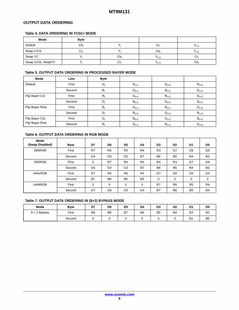
OUTPUT DATA ORDERING
Table 4. DATA ORDERING IN YCbCr MODE
Mode Byte
Default Cbi Yi Cri Yi+1
Swap CrCb Cri Yi Cbi Yi+1
Swap YC Yi Cbi Yi+1 Cri
Swap CrCb, SwapYC Yi Cri Yi+1 Cbi
Table 5. OUTPUT DATA ORDERING IN PROCESSED BAYER MODE
Mode Line Byte
Default First Gi Ri+1 Gi+2 Ri+3
Second Bi Gi+1 Bi+2 Gi+3
Flip Bayer Col First Ri Gi+1 Ri+2 Gi+3
Second Gi Bi+1 Gi+2 Bi+3
Flip Bayer Row First Bi Gi+1 Bi+2 Gi+3
Second Gi Ri+1 Gi+2 Ri+3
Flip Bayer Col,Flip Bayer Row
First Gi Bi+1 Gi+2 Bi+3
Second Ri Gi+1 Ri+2 Gi+3
Table 6. OUTPUT DATA ORDERING IN RGB MODE
Mode(Swap Disabled) Byte D7 D6 D5 D4 D3 D2 D1 D0
565RGB First R7 R6 R5 R4 R3 G7 G6 G5
Second G4 G3 G2 B7 B6 B5 B4 B3
555RGB First 0 R7 R6 R5 R4 R3 G7 G6
Second G5 G4 G3 B7 B6 B5 B4 B3
444xRGB First R7 R6 R5 R4 G7 G6 G5 G4
Second B7 B6 B5 B4 0 0 0 0
x444RGB First 0 0 0 0 R7 R6 R5 R4
Second G7 G6 G5 G4 B7 B6 B5 B4
Table 7. OUTPUT DATA ORDERING IN (8+2) BYPASS MODE
Mode Byte D7 D6 D5 D4 D3 D2 D1 D0
8 + 2 Bypass First B9 B8 B7 B6 B5 B4 B3 B2
Second 0 0 0 0 0 0 B1 B0

MT9M131
www.onsemi.com9
IFP REGISTER LIST
Table 8. COLORPIPE REGISTERS (ADDRESS PAGE 1)
Register NumberDec (Hex) Register Name
Data Format(Binary)
Default ValueDec (Hex) Module
R5 (R0x105) Aperture Correction 0000 0000 0000 dddd 3 (0003) Interp
R6 (R0x106) Operating Mode Control dddd dddd 0ddd dddd 28686 (700E) Cfg
R8 (R0x108) Output Format Control 0000 0ddd dddd dddd 128 (0080) Cfg
R16 (R0x110) Reserved – 61437 (EFFD) –
R17 (R0x111) Reserved – 64831 (FD3F) –
R18 (R0x112) Reserved – 16367 (3FEF) –
R19 (R0x113) Reserved – N/A –
R20 (R0x114) Reserved – N/A –
R21 (R0x115) Reserved – N/A –
R27 (R0x11B) Reserved – 0 (0000) –
R28 (R0x11C) Reserved – 0 (0000) –
R29 (R0x11D) Reserved – N/A –
R30 (R0x11E) Reserved – 512 (0200) –
R37 (R0x125) Color Saturation Control 0000 0000 00dd dddd 5 (0005) rgb2yuv
R52 (R0x134) Luma Offset dddd dddd dddd dddd 16 (0010) Camlnt
R53 (R0x135) Luma Clip dddd dddd dddd dddd 61456 (F010) Camlnt
R58 (R0x13A) Output Format Control 2 − Context A 0ddd dddd dddd dddd 512 (0200) CamInt
R59 (R0x13B) 1066 (042A) LensCorr
R60 (R0x13C) 1024 (0400) LensCorr
R71 (R0x147) 24 (0018)
R72 (R0x148) Test Pattern Generator Control 0000 0000 d000 0ddd 0 (0000) FifoInt
R76 (R0x14C) Defect Correction Context A 0000 0000 0000 0ddd 0 (0000) DfctCorr
R77 (R0x14D) Defect Correction Context B 0000 0000 0000 0ddd 0 (0000) DfctCorr
R78 (R0x14E) Reserved – 10 (000A) –
R80 (R0x150) N/A
R82 (R0x152) Reserved – 0 (0000) –
R83 (R0x153) 7700 (1E14) GmaCorr
R84 (R0x154) 17966 (462E) GmaCorr
R85 (R0x155) 34666 (876A) GmaCorr
R86 (R0x156) 47008 (B7A0) GmaCorr
R87 (R0x157) 57548 (E0CC) GmaCorr
R88 (R0x158) 0 (0000) GmaCorr
R104 (R0x168) Reserved – 17 (0011) –
R128 (R0x180) 7 (0007) LensCorr
R129 (R0x181) 56588 (DD0C) LensCorr
R130 (R0x182) 62696 (F4E8) LensCorr
R131 (R0x183) 1276 (04FC) LensCorr
R132 (R0x184) 57868 (E20C) LensCorr
R133 (R0x185) 63212 (F6EC) LensCorr
R134 (R0x186) 764 (02FC) LensCorr
R135 (R0x187) 56588 (DD0C) LensCorr
R136 (R0x188) 62696 (F4E8) LensCorr
R137 (R0x189) 250 (00FA) LensCorr

MT9M131
www.onsemi.com10
Table 8. COLORPIPE REGISTERS (ADDRESS PAGE 1) (continued)
Register NumberDec (Hex) Module
Default ValueDec (Hex)
Data Format(Binary)Register Name
R138 (R0x18A) 34866 (8832) LensCorr
R139 (R0x18B) 56754 (DDB2) LensCorr
R140 (R0x18C) 63466 (F7EA) LensCorr
R141 (R0x18D) 2 (0002) LensCorr
R142 (R0x18E) 47646 (BA1E) LensCorr
R143 (R0x18F) 60627 (ECD3) LensCorr
R144 (R0x190) 63473 (F7F1) LensCorr
R145 (R0x191) 255 (00FF) LensCorr
R146 (R0x192) 48926 (BF1E) LensCorr
R147 (R0x193) 61142 (EED6) LensCorr
R148 (R0x194) 63474 (F7F2) LensCorr
R149 (R0x195) 3 (0003) LensCorr
R153 (R0x199) Line Counter ???? ???? ???? ???? N/A CamInt
R154 (R0x19A) Frame Counter ???? ???? ???? ???? N/A CamInt
R155 (R0x19B) Output Format Control 2 − Context B 0ddd dddd dddd dddd 512 (0200) CamInt
R157 (R0x19D) Reserved – 9390 (24AE) –
R158 (R0x19E) Reserved – N/A –
R159 (R0x19F) Reducer Gorizontal Pan − Context B 0d00 0ddd dddd dddd 0 (0000) Interp
R160 (R0x1A0) Reducer Horizontal Zoom − Context B 0000 0ddd dddd dddd 1280 (0500) Interp
R161 (R0x1A1) Reducer Horizontal Size − Context B 0000 0ddd dddd dddd 1280 (0500) Interp
R162 (R0x1A2) Reducer Vertical Pan − Context B 0d00 0ddd dddd dddd 0 (0000) Interp
R163 (R0x1A3) Reducer Vertical Zoom − Context B 0000 0ddd dddd dddd 1024 (0400) Interp
R164 (R0x1A4) Reducer Vertical Size − Context B 0000 0ddd dddd dddd 1024 (0400) Interp
R165 (R0x1A5) Reducer Horizontal Pan − Context A 0d00 0ddd dddd dddd 0 (0000) Interp
R166 (R0x1A6) Reducer Horizontal Zoom − Context A 0000 0ddd dddd dddd 1280 (0500) Interp
R167 (R0x1A7) Reducer Horizontal Size − Context A 0000 0ddd dddd dddd 640 (0280) Interp
R168 (R0x1A8) Reducer Vertical Pan − Context A 0d00 0ddd dddd dddd 0 (0000) Interp
R169 (R0x1A9) Reducer Vertical Zoom − Context A 0000 0ddd dddd dddd 1024 (0400) Interp
R170 (R0x1AA) Reducer Vertical Size − Context A 0000 0ddd dddd dddd 512 (0200) Interp
R171 (R0x1AB) Reducer Current Zoom Horizontal ???? 0??? ???? ???? N/A Interp
R172 (R0x1AC) Reducer Current Zoom Vertical ???? 0??? ???? ???? N/A Interp
R174 (R0x1AE) Reducer Zoom Step Size dddd dddd dddd dddd 1284 (0504) Interp
R175 (R0x1AF) Reducer Zoom Control 0000 00dd 0ddd dddd 16 (0010) Interp
R179 (R0x1B3) Global Clock Control 0000 0000 0000 00dd 2 (0002) ClockRst
R180 (R0x1B4) 32 (0020)
R181 (R0x1B5) 257 (0101)
R182 (R0x1B6) 4363 (110B) LensCorr
R183 (R0x1B7) 15399 (3C27) LensCorr
R184 (R0x1B8) 4362 (110A) LensCorr
R185 (R0x1B9) 12834 (3222) LensCorr
R186 (R0x1BA) 5643 (160B) LensCorr
R187 (R0x1BB) 12836 (3224) LensCorr
R188 (R0x1BC) 9228 (240C) LensCorr
R189 (R0x1BD) 24124 (5E3C) LensCorr
R190 (R0x1BE) 127 (007F) LensCorr

MT9M131
www.onsemi.com11
Table 8. COLORPIPE REGISTERS (ADDRESS PAGE 1) (continued)
Register NumberDec (Hex) Module
Default ValueDec (Hex)
Data Format(Binary)Register Name
R191 (R0x1BF) 8200 (2008) LensCorr
R192 (R0x1C0) 20023 (4E37) LensCorr
R193 (R0x1C1) 100 (0064) LensCorr
R194 (R0x1C2) 8463 (210F) LensCorr
R195 (R0x1C3) 19250 (4B32) LensCorr
R196 (R0x1C4) 100 (0064) LensCorr
R200 (R0x1C8) Global Context Control dddd dddd dddd dddd 0 (0000) CntxCtl
R201 (R0x1C9) Reserved – N/A –
R202 (R0x1CA) Reserved – N/A –
R203 (R0x1CB) Reserved – N/A –
R204 (R0x1CC) Reserved – N/A –
R205 (R0x1CD) Reserved – N/A –
R206 (R0x1CE) Reserved – N/A –
R207 (R0x1CF) Reserved – N/A –
R208 (R0x1D0) Reserved – N/A –
R220 (R0x1DC) 7700 (1E14) GmaCorr
R221 (R0x1DD) 17966 (462E) GmaCorr
R222 (R0x1DE) 34666 (876A) GmaCorr
R223 (R0x1DF) 47008 (B7A0) GmaCorr
R224 (R0x1E0) 57548 (E0CC) GmaCorr
R225 (R0x1E1) 0 (0000) GmaCorr
R226 (R0x1E2) Effects Mode dddd dddd 0000 0ddd 28672 (7000) GmaCorr
R227 (R0x1E3) Effects Sepia dddd dddd dddd dddd 45091 (B023) GmaCorr
R240 (R0x1F0) Page Map 0000 0000 0000 0ddd 0 (0000) Cfg
R241 (R0x1F1) Byte-wise Address – Reserved –

MT9M131
www.onsemi.com12
Table 9. CAMERA CONTROL REGISTERS (ADDRESS PAGE 2)
Register NumberDec (Hex) Register Name
Data Format(Binary)
Default ValueDec (Hex) Module
R2 (R0x202) 110 (006E) ColorCorr
R3 (R0x203) 10531 (2923) ColorCorr
R4 (R0x204) 1316 (0524) ColorCorr
R9 (R0x209) 146 (0092) ColorCorr
R10 (R0x20A) 22 (0016) ColorCorr
R11 (R0x20B) 8 (0008) ColorCorr
R12 (R0x20C) 171 (00AB) ColorCorr
R13 (R0x20D) 147 (0093) ColorCorr
R14 (R0x20E) 88 (0058) ColorCorr
R15 (R0x20F) 77 (004D) ColorCorr
R16 (R0x210) 169 (00A9) ColorCorr
R17 (R0x211) 160 (00A0) ColorCorr
R18 (R0x212) N/A ColorCorr
R19 (R0x213) N/A ColorCorr
R20 (R0x214) N/A ColorCorr
R21 (R0x215) 373 (0175) ColorCorr
R22 (R0x216) 22 (0016) ColorCorr
R23 (R0x217) 67 (0043) ColorCorr
R24 (R0x218) 12 (000C) ColorCorr
R25 (R0x219) 0 (0000) ColorCorr
R26 (R0x21A) 21 (0015) ColorCorr
R27 (R0x21B) 31 (001F) ColorCorr
R28 (R0x21C) 22 (0016) ColorCorr
R29 (R0x21D) 152 (0098) ColorCorr
R30 (R0x21E) 76 (004C) ColorCorr
R31 (R0x21F) 160 (00A0) AWB
R32 (R0x220) 51220 (C814) AWB
R33 (R0x221) 32896 (8080) AWB
R34 (R0x222) 55648 (D960) AWB
R35 (R0x223) 55648 (D960) AWB
R36 (R0x224) 32512 (7F00) AWB
R38 (R0x226) Auto Exposure Window HorizontalBoundaries
dddd dddd dddd dddd 32768 (8000) AutoExp
R39 (R0x227) Auto Exposure Window VerticalBoundaries
dddd dddd dddd dddd 32776 (8008) AutoExp
R40 (R0x228) 61188 (EF04) AWB
R41 (R0x229) 36211 (8D73) AWB
R42 (R0x22A) 208 (00D0) AWB
R43 (R0x22B) Auto Exposure Center HorizontalWindow Boundaries
dddd dddd dddd dddd 24608 (6020) AutoExp
R44 (R0x22C) Auto Exposure Center VerticalWindow Boundaries
dddd dddd dddd dddd 24608 (6020) AutoExp
R45 (R0x22D) AWB Window Boundaries dddd dddd dddd dddd 61600 (F0A0) AWB
R46 (R0x22E) Auto Exposure Target and PrecisionControl
dddd dddd dddd dddd 3146 (0C4A) AutoExp

MT9M131
www.onsemi.com13
Table 9. CAMERA CONTROL REGISTERS (ADDRESS PAGE 2) (continued)
Register NumberDec (Hex) Module
Default ValueDec (Hex)
Data Format(Binary)Register Name
R47 (R0x22F) Auto Exposure Speed and SensitivityControl − Context A
dddd dddd dddd dddd 57120 (DF20) AutoExp
R48 (R0x230) N/A AWB
R49 (R0x231) N/A AWB
R50 (R0x232) N/A AWB
R51 (R0x233) 5230 (146E) AutoExp
R54 (R0x236) 30736 (7810) AutoExp
R55 (R0x237) 768 (0300) AutoExp
R56 (R0x238) 1088 (0440) AutoExp
R57 (R0x239) 1676 (068C) AutoExp
R58 (R0x23A) 1676 (068C) AutoExp
R59 (R0x23B) 1676 (068C) AutoExp
R60 (R0x23C) 1676 (068C) AutoExp
R61 (R0x23D) 6105 (17D9) AutoExp
R62 (R0x23E) 7423 (1CFF) AWB
R63 (R0x23F) N/A AutoExp
R70 (R0x246) 55552 (D900) AutoExp
R75 (R0x24B) Reserved – 0 (0000) –
R76 (R0x24C) N/A AutoExp
R77 (R0x24D) N/A AutoExp
R79 (R0x24F) Reserved – N/A –
R87 (R0x257) 537 (0219) AutoExp
R88 (R0x258) 644 (0284) AutoExp
R89 (R0x259) 537 (0219) AutoExp
R90 (R0x25A) 644 (0284) AutoExp
R91 (R0x25B) Flicker Control 0 ?000 0000 0000 0ddd 2 (0002) FD
R92 (R0x25C) 4620 (120C)
R93 (R0x25D) 5394 (1512)
R94 (R0x25E) 26684 (683C) ColorCorr
R95 (R0x25F) 12296 (3008) ColorCorr
R96 (R0x260) 2 (0002) ColorCorr
R97 (R0x261) 32896 (8080)
R98 (R0x262) Auto Exposure Digital Gains Monitor ???? ???? ???? ???? N/A AutoExp
R99 (R0x263) Reserved – N/A –
R100 (R0x264) Reserved – 23036 (59FC) –
R101 (R0x265) 0 (0000) AutoExp
R103 (R0x267) Auto Exposure Digital Gain Limits dddd dddd dddd dddd 16400 (4010) AutoExp
R104 (R0x268) Reserved – 17 (0011) –
R106 (R0x26A) Reserved – N/A –
R107 (R0x26B) Reserved – N/A –
R108 (R0x26C) Reserved – N/A –
R109 (R0x26D) Reserved – N/A –
R110 (R0x26E) Reserved – N/A –
R111 (R0x26F) Reserved – N/A –
R112 (R0x270) Reserved – N/A –

MT9M131
www.onsemi.com14
Table 9. CAMERA CONTROL REGISTERS (ADDRESS PAGE 2) (continued)
Register NumberDec (Hex) Module
Default ValueDec (Hex)
Data Format(Binary)Register Name
R113 (R0x271) Reserved – N/A –
R114 (R0x272) Reserved – N/A –
R115 (R0x273) Reserved – N/A –
R116 (R0x274) Reserved – N/A –
R117 (R0x275) Reserved – N/A –
R118 (R0x276) Reserved – N/A –
R119 (R0x277) Reserved – N/A –
R120 (R0x278) Reserved – N/A –
R121 (R0x279) Reserved – N/A –
R122 (R0x27A) Reserved – N/A –
R123 (R0x27B) Reserved – N/A –
R124 (R0x27C) Reserved – N/A –
R125 (R0x27D) Reserved – N/A –
R130 (R0x282) 1020 (03FC) AutoExp
R131 (R0x283) 769 (0301) AutoExp
R132 (R0x284) 193 (00C1) AutoExp
R133 (R0x285) 929 (03A1) AutoExp
R134 (R0x286) 980 (03D4) AutoExp
R135 (R0x287) 983 (03D7) AutoExp
R136 (R0x288) 921 (0399) AutoExp
R137 (R0x289) 1016 (03F8) AutoExp
R138 (R0x28A) 28 (001C) AutoExp
R139 (R0x28B) 957 (03BD) AutoExp
R140 (R0x28C) 987 (03DB) AutoExp
R141 (R0x28D) 957 (03BD) AutoExp
R142 (R0x28E) 1020 (03FC) AutoExp
R143 (R0x28F) 990 (03DE) AutoExp
R144 (R0x290) 990 (03DE) AutoExp
R145 (R0x291) 990 (03DE) AutoExp
R146 (R0x292) 990 (03DE) AutoExp
R147 (R0x293) 31 (001F) AutoExp
R148 (R0x294) 65 (0041) AutoExp
R149 (R0x295) 867 (0363) AutoExp
R150 (R0x296) Reserved – 0 (0000) –
R151 (R0x297) Reserved – N/A –
R152 (R0x298) Reserved – 255 (00FF) –
R153 (R0x299) Reserved – 1 (0001) –
R156 (R0x29C) Auto Exposure Speed and SensitivityControl − Context B
dddd dddd dddd dddd 57120 (DF20) AutoExp
R180 (R0x2B4) Reserved – 32 (0020) –
R181 (R0x2B5) Reserved – N/A –
R198 (R0x2C6) Reserved – 0 (0000) –
R199 (R0x2C7) Reserved – N/A –
R200 (R0x2C8) Global Context Control dddd dddd dddd dddd 0 (0000) CntxCtl
R201 (R0x2C9) N/A CamCtl

MT9M131
www.onsemi.com15
Table 9. CAMERA CONTROL REGISTERS (ADDRESS PAGE 2) (continued)
Register NumberDec (Hex) Module
Default ValueDec (Hex)
Data Format(Binary)Register Name
R202 (R0x2CA) N/A CamCtl
R203 (R0x2CB) 0 (0000) CamCtl
R204 (R0x2CC) 0 (0000) CamCtl
R205 (R0x2CD) 8608 (21A0) CamCtl
R206 (R0x2CE) 7835 (1E9B) CamCtl
R207 (R0x2CF) 19018 (4A4A) CamCtl
R208 (R0x2D0) 5773 (168D) CamCtl
R209 (R0x2D1) 77 (004D) CamCtl
R210 (R0x2D2) 0 (0000) CamCtl
R211 (R0x2D3) 0 (0000) CntxCtl
R212 (R0x2D4) 520 (0208) CamCtl
R213 (R0x2D5) 0 (0000) CamCtl
R239 (R0x2EF) 8 (0008) AWB
R240 (R0x2F0) Page Map 0000 0000 0000 0ddd 0 (0000) Cfg
R241 (R0x2F1) Byte-wise Address – Reserved –
R242 (R0x2F2) 0 (0000) AWB
R243 (R0x2F3) Reserved – 0 (0000) –
R244 (R0x2F4) 110 (006E) ColorCorr
R245 (R0x2F5) 135 (0087) ColorCorr
R246 (R0x2F6) 54 (0036) ColorCorr
R247 (R0x2F7) 13 (000D) ColorCorr
R248 (R0x2F8) 171 (00AB) ColorCorr
R249 (R0x2F9) 136 (0088) ColorCorr
R250 (R0x2FA) 72 (0048) ColorCorr
R251 (R0x2FB) 87 (0057) ColorCorr
R252 (R0x2FC) 94 (005E) ColorCorr
R253 (R0x2FD) 122 (007A) ColorCorr
R254 (R0x2FE) 20543 (503F) ColorCorr
R255 (R0x2FF) 43136 (A880) ColorCorr
NOTE: Data Format Key:0 = “Don’t Care” bit. The exceptions: R0x200 and R0x2FF, which are hardwired R/O binary valuesd = R/W bit? = R/O bit

MT9M131
www.onsemi.com16
IFP REGISTER DESCRIPTION
ConfigurationThe vast majority of IFP registers associate naturally to
one of the IFP modules. These modules are identified inTable 9. Detailed register descriptions follow in Table 10.A few registers create effects across a number of modulefunctions. These include R0xF0 page map register (R/W);R0x106 operating mode control register (R/W); R0x108output format control register (R/W); the R0x23E gain typesand CCM threshold register − the gain threshold for CCMadjustment (R/W).
Colorpipe RegistersUnless noted otherwise in this document, colorpipe
registers take effect immediately. This can result in one ormore distorted output frames. These registers should beadjusted during FV LOW or the resulting image should behidden for one or two frames.
Colorpipe resize registers are updated shortly after FVgoes HIGH. They are not examined again until the nextframe.
Table 10. COLORPIPE REGISTER DESCRIPTION ADDRESS PAGE 1
Register NumberDec − Hex Description
R5:1 − R0x105 − Aperture Correction
Default 0x0003
Description Aperture correction scale factor, used for sharpening
Bit 3 Enables automatic sharpness reduction control (see R0x233)
Bits 2:0 Sharpening factor: “000” − No sharpening“001” − 25% sharpening“010” − 50% sharpening“011” − 75% sharpening“100” − 100% sharpening“101” − 125% sharpening“110” − 150% sharpening“111” − 200% sharpening
R6:1 − R0x106 − Operating Mode Control (R/W)
Default 0x700E
Description This register specifies the operating mode of the IFP
Bit 15 Enables manual white balance. User can set the base matrix and color channel gains. This bit must be assertedand de-asserted with a frame in between to force new color correction settings to take effect
Bit 14 Enables auto exposure
Bit 13 Enables on-the-fly defect correction
Bit 12 Clips aperture corrections. Small aperture corrections (< 8) are attenuated to reduce noise amplification
Bit 11 Load color correction matrix1: In manual white balance mode, triggers the loading of a new base matrix in color correction and the loading
of new base sensor gain ratios0: Enables the matrix to be changed “offline”
Bit 10 Enables lens shading correction1: Enables lens shading correction
Bit 9 Reserved
Bit 8 Reserved
Bit 7 Enables flicker detection1: Enables automatic flicker detection
Bit 6 Reserved for future expansion
Bit 5 Reserved
Bit 4 Bypasses color correction matrix1: Outputs raw color, bypassing color correction0: Normal color processing
Bits 3:2 Auto exposure back light compensation control“00” − Auto exposure sampling window is specified by R0x226 and R0x227 (“large window”)“01” − Auto exposure sampling window is specified by R0x22B and R0x22C (“small window”)“1X” − Auto exposure sampling window is specified by the weighted sum of the large window and the small window, with the small window weighted four times more heavily

MT9M131
www.onsemi.com17
Table 10. COLORPIPE REGISTER DESCRIPTION ADDRESS PAGE 1 (continued)
Register NumberDec − Hex Description
Bit 1 Enables AWB1: Enables auto white balance0: Freezes white balance at current values
Bit 0 Reserved for future expansion.
R8:1 − R0x108 − Output Format Control (R/W)
Default 0x0080
Description This register specifies the output timing and format in conjunction with R0x13A or R0x19B (depending on thecontext)
Bits 15:10 Reserved for future expansion
Bit 9 Flip Bayer columns in processed Bayer output mode0: Column order is green, red and blue, green.1: Column order is red, green and green, blue.
Bit 8 Flip Bayer row in processed Bayer output mode0: First row contains green and red; the second row contains blue and green1: First row contains blue and green; the second row contains green and red
Bit 7 Controls the values used for the protection bits in Rec. ITU−R BT.656 codes0: Use zeros for the protection bits1: Use the correct values
Bit 5 Multiplexes Y (in YCbCr mode) or green (in RGB mode) channel on all channels (monochrome)1: Forces Y/G onto all channels
Bit 4 Disables Cab color output channel (Cb = 128) in YCbCr mode and disables the blue color output channel (B = 0) in RGB mode
1: Forces Cab to 128 or B to 0
Bit 3 Disables Y color output channel (Y = 128) in YCbCr and disables the green color output channel (G = 0) in RGBmode
1: Forces Y to 128 or G to 0
Bit 2 Disables Cr color output channel (Cr = 128) in YCbCr mode and disables the red color output channel (R = 0) inRGB mode
1: Forces Cr to 128 or R to 0
Bit 1 Toggles the assumptions about Bayer vertical CFA shift0: Row containing red comes first1: Row containing blue comes first
Bit 0 Toggles the assumptions about Bayer horizontal CFA shift0: Green comes first1: Red or blue comes first
R37:1 − R0x125 − Color Saturation Control (R/W)
Default 0x0005
Description This register specifies the color saturation control settings.
Bit 5:3 Specify overall attenuation of the color saturation“000” − Full color saturation“001” − 75% of full saturation“010” − 50% of full saturation“011” − 37.5% of full saturation“100” − 25% of full saturation“101” − 150% of full saturation“110” − black and white
Bit 2:0 Specify color saturation attenuation at high luminance (linearly increasing attenuation from no attenuation tomonochrome at luminance of 224).
“000” − No attenuation“001” − Attenuation starts at luminance of 216“010” − Attenuation starts at luminance of 208“011” − Attenuation starts at luminance of 192“100” − Attenuation starts at luminance of 160“101” − Attenuation starts at luminance of 96
MT9M131
www.onsemi.com18
Table 10. COLORPIPE REGISTER DESCRIPTION ADDRESS PAGE 1 (continued)
Register NumberDec − Hex Description
R52:1 − R0x134 − Luma Offset (R/W)
Default 0x0010
Description Offset added to the luminance prior to output
Bits 15:8 Y Offset in YCbCr mode
Bits 7:0 Offset in RGB mode
R53:1 − R0x135 − Luma Clip (R/W)
Default 0xF010
Description Clipping limits for output luminance
Bits 15:8 Highest value of output luminance
Bits 7:0 Lowest value of output luminance
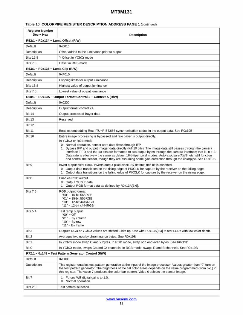
R58:1 − R0x13A − Output Format Control 2 − Context A (R/W)
Default 0x0200
Description Output format control 2A
Bit 14 Output processed Bayer data
Bit 13 Reserved
Bit 12
Bit 11 Enables embedding Rec. ITU−R BT.656 synchronization codes in the output data. See R0x19B
Bit 10 Entire image processing is bypassed and raw bayer is output directly.In YCbCr or RGB mode:
0: Normal operation, sensor core data flows through IFP.1: Bypass IFP and output Imager data directly (full 10 bits). The image data still passes through the camera
interface FIFO and the 10 bits are formatted to two output bytes through the camera interface; that is, 8 + 2.Data rate is effectively the same as default 16-bit/per pixel modes. Auto exposure/AWB, etc. still functionand control the sensor, though they are assuming some gain/correction through the colorpipe. See R0x19B
Bit 9 Invert output pixel clock. Inverts output pixel clock. By default, this bit is asserted.0: Output data transitions on the rising edge of PIXCLK for capture by the receiver on the falling edge.1: Output data transitions on the falling edge of PIXCLK for capture by the receiver on the rising edge.
Bit 8 Enables RGB output.0: Output YCbCr data.1: Output RGB format data as defined by R0x13A[7:6].
Bits 7:6 RGB output format:“00” − 16-bit 565RGB“01” − 15-bit 555RGB“10” − 12-bit 444xRGB“11” − 12-bit x444RGB
Bits 5:4 Test ramp output:“00” − Off“01” − By column“10” − By row“11” − By frame
Bit 3 Outputs RGB or YCbCr values are shifted 3 bits up. Use with R0x13A[5:4] to test LCDs with low color depth.
Bit 2 Averages two nearby chrominance bytes. See R0x19B
Bit 1 In YCbCr mode swap C and Y bytes. In RGB mode, swap odd and even bytes. See R0x19B
Bit 0 In YCbCr mode, swaps Cb and Cr channels. In RGB mode, swaps R and B channels. See R0x19B
R72:1 − 0x148 − Test Pattern Generator Control (R/W)
Default 0x0000
Description This register enables test pattern generation at the input of the image processor. Values greater than “0” turn onthe test pattern generator. The brightness of the flat color areas depends on the value programmed (from 6–1) inthis register. The value 7 produces the color bar pattern. Value 0 selects the sensor image.
Bit 7 1: Forces WB digital gains to 1.0.0: Normal operation.
Bits 2:0 Test pattern selection

MT9M131
www.onsemi.com19
Table 10. COLORPIPE REGISTER DESCRIPTION ADDRESS PAGE 1 (continued)
Register NumberDec − Hex Description
R76:1 − 0x14C − Defect Correction − Context A (R/W)
Default 0x0000
Description Context A register with defect correction, mode enables, and calibration bits
Bit 2 Reserved
Bit 1 Reserved
Bit 0 Enables 2D defect correction
R77:1 − 0x14D − Defect Correction − Context B (R/W)
Default 0x0000
Description Context B register with defect correction, mode enables, and calibration bits
Bit 2 Reserved
Bit 1 Reserved
Bit 0 Enables 2D defect correction
R153:1 − 0x199 − Line Counter (R/O)
Default N/A
Description Use line counter to determine the number of the line currently being output
Bits 12:0 Line count
R154:1 − 0x19A − Frame Counter (R/O)
Default N/A
Description Use frame counter to determine the index of the frame currently being output
Bits 15:0 Frame count
R155:1 − 0x19B − Output Format Control 2 — Context B (R/W)
Default 0x0200
Description Output format control 2B
Bit 14 Output processed Bayer data
Bit 13 Reserved
Bit 12
Bit 11 Enables embedding Rec. ITU−R BT.656 synchronization codes to the output data. See R0x13A
Bit 10 Entire image processing is bypassed and raw bayer is output directly.In YCbCr or RGB mode:
0: Normal operation, sensor core data flows through IFP.1: Bypass IFP and output Imager data directly (full 10 bits). The image data still passes through the camera
interface FIFO and the 10 bits are formatted to 2 output bytes through the camera interface; that is, 8 + 2.Data rate is effectively the same as default 16-bit /per pixel modes. AE/AWB, and so on, still function andcontrol the sensor, though they are assuming some gain/correction through the colorpipe. See R0x13A.
Bit 9 Invert output pixel clock. Inverts output pixel clock. By default, this bit is asserted.0: Output data transitions on the rising edge of PIXCLK for capture by the receiver on the falling edge.1: Output data transitions on the falling edge of PIXCLK for capture by the receiver on the rising edge.
Bit 8 Enables RGB output.0: Output YCbCr data.1: Output RGB format data as defined by R0x19B[7:6]. See R0x13A.
Bits 7:6 RGB output format:“00” − 16-bit 565RGB“01” − 15-bit 555RGB“10” − 12-bit 444xRGB“11” − 12-bit x444RGB
Bits 5:4 Test Ramp output:“00” − Off“01” − By column“10” − By row“11” − By frame
Bit 3 Output RGB or YCbCr values are shifted 3 bits up. Use with R0x13A[5:4] to test LCDs with low color depth
MT9M131
www.onsemi.com20
Table 10. COLORPIPE REGISTER DESCRIPTION ADDRESS PAGE 1 (continued)
Register NumberDec − Hex Description
Bit 2 Averages two nearby chrominance bytes. See R0x13A
Bit 1 In YCbCr mode swap C and Y bytes. In RGB mode, swap odd and even bytes. See R0x13A
Bit 0 In YCbCr mode, swaps Cb and Cr channels. In RGB mode, swaps R and B channels. See R0x13A
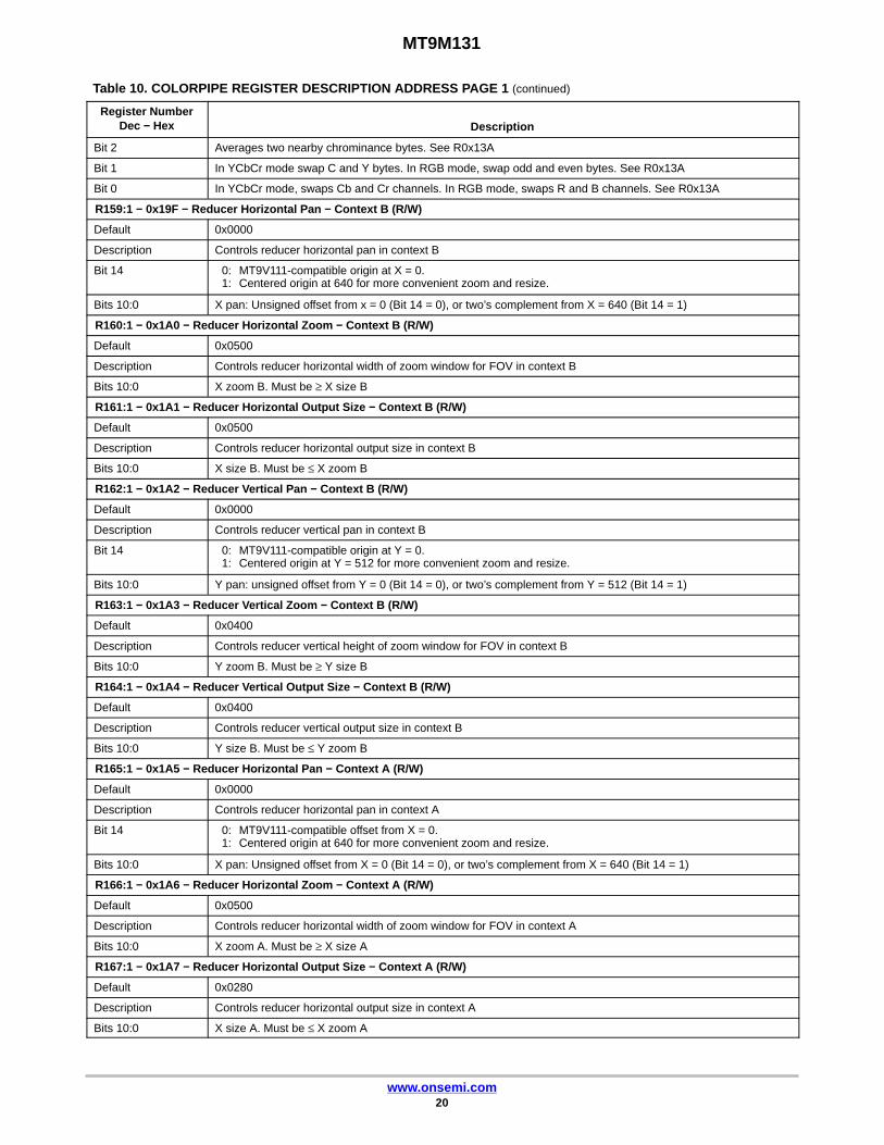
R159:1 − 0x19F − Reducer Horizontal Pan − Context B (R/W)
Default 0x0000
Description Controls reducer horizontal pan in context B
Bit 14 0: MT9V111-compatible origin at X = 0.1: Centered origin at 640 for more convenient zoom and resize.
Bits 10:0 X pan: Unsigned offset from x = 0 (Bit 14 = 0), or two’s complement from X = 640 (Bit 14 = 1)
R160:1 − 0x1A0 − Reducer Horizontal Zoom − Context B (R/W)
Default 0x0500
Description Controls reducer horizontal width of zoom window for FOV in context B
Bits 10:0 X zoom B. Must be ≥ X size B
R161:1 − 0x1A1 − Reducer Horizontal Output Size − Context B (R/W)
Default 0x0500
Description Controls reducer horizontal output size in context B
Bits 10:0 X size B. Must be ≤ X zoom B
R162:1 − 0x1A2 − Reducer Vertical Pan − Context B (R/W)
Default 0x0000
Description Controls reducer vertical pan in context B
Bit 14 0: MT9V111-compatible origin at Y = 0.1: Centered origin at Y = 512 for more convenient zoom and resize.
Bits 10:0 Y pan: unsigned offset from Y = 0 (Bit 14 = 0), or two’s complement from Y = 512 (Bit 14 = 1)
R163:1 − 0x1A3 − Reducer Vertical Zoom − Context B (R/W)
Default 0x0400
Description Controls reducer vertical height of zoom window for FOV in context B
Bits 10:0 Y zoom B. Must be ≥ Y size B
R164:1 − 0x1A4 − Reducer Vertical Output Size − Context B (R/W)
Default 0x0400
Description Controls reducer vertical output size in context B
Bits 10:0 Y size B. Must be ≤ Y zoom B
R165:1 − 0x1A5 − Reducer Horizontal Pan − Context A (R/W)
Default 0x0000
Description Controls reducer horizontal pan in context A
Bit 14 0: MT9V111-compatible offset from X = 0.1: Centered origin at 640 for more convenient zoom and resize.
Bits 10:0 X pan: Unsigned offset from X = 0 (Bit 14 = 0), or two’s complement from X = 640 (Bit 14 = 1)
R166:1 − 0x1A6 − Reducer Horizontal Zoom − Context A (R/W)
Default 0x0500
Description Controls reducer horizontal width of zoom window for FOV in context A
Bits 10:0 X zoom A. Must be ≥ X size A
R167:1 − 0x1A7 − Reducer Horizontal Output Size − Context A (R/W)
Default 0x0280
Description Controls reducer horizontal output size in context A
Bits 10:0 X size A. Must be ≤ X zoom A

MT9M131
www.onsemi.com21
Table 10. COLORPIPE REGISTER DESCRIPTION ADDRESS PAGE 1 (continued)
Register NumberDec − Hex Description
R168:1 − 0x1A8 − Reducer Vertical Pan − Context A (R/W)
Default 0x0000
Description Controls reducer vertical pan in context A
Bit 14 0: MT9V111-compatible origin at Y = 0.1: Centered origin at Y = 512 for more convenient zoom and resize.
Bits 10:0 Y pan: unsigned offset from y = 0 (Bit 14 = 0), or two s complement from Y = 512 (Bit 14 = 1)
R169:1 − 0x1A9 − Reducer Vertical Zoom − Context A (R/W)
Default 0x0400
Description Controls reducer vertical height of zoom window for FOV in context A
Bits 10:0 Y zoom A. Must be ≥ Y size A
R170:1 − 0x1AA − Reducer Vertical Output Size — Context A (R/W)
Default 0x0200
Description Controls reducer vertical output size in context A
Bits 10:0 Y size A. Must be ≤ Y zoom A
R171:1 − 0x1AB − Reducer Current Horizontal Zoom (R/O)
Default N/A
Description Current horizontal zoom
Bits 10:0 Current zoom Window Width. After automatic zoom (R0x1AF), copy R0x1AB to the snapshot X zoom registerR0x1A6 (context A) or R0x1A0 (context B) so the snapshot has the same FOV as preview. Also copy tosnapshot X size register R0x1A7 (context A) or R0x1A1 (context B) for largest snapshot.
Bits 15:12 Reserved. Mask off these bits before performing the above copy operation
R172:1 − 0x1AC − Reducer Current Vertical Zoom (R/O)
Default N/A
Description Current vertical zoom
Bits 10:0 Current zoom Window Height. After automatic zoom (R0x1AF), copy R0x1AC to the snapshot Y zoom registerR0x1A9 (context A) or R0x1A3 (context B) so the snapshot will have the same FOV as preview. Also copy tosnapshot X size register R0x1AA (context A) or R0x1A4 (context B) for largest snapshot.
Bits 15:12 Reserved. Mask off these bits before performing the above copy operation
R174:1 − 0x1AE − Reducer Zoom Step Size (R/W)
Default 0x0504
Description Zoom step sizes. Should be a multiple of the aspect ratio 5:4 for SXGA or 4:3 VGA or 11:9 for CIF
Bits 15:8 Zoom step size in X
Bits 7:0 Zoom step size in Y
R175:1 − 0x1AF − Reducer Zoom Control (R/W)
Default 0x0010
Description Resize interpolation and zoom control
Bit 9 Starts automatic “zoom out” in step sizes defined in R0x1AE
Bit 8 Starts automatic “zoom in” in step sizes defined in R0x1AE
Bit 6
Bit 5
Bit 4
Bit 3 Auto switch to classic interpolation at full resolution
Bit 1 Reserved
Bit 0 Reserved

MT9M131
www.onsemi.com22
Table 10. COLORPIPE REGISTER DESCRIPTION ADDRESS PAGE 1 (continued)
Register NumberDec − Hex Description
R179:1 − 0x1B3 − Global Clock Control (R/W)
Default 0x0002
Description Configures assorted aspects of the clock controller
Bits 15:2 Not used
Bit 1 Tri-states signals in standby mode
Bit 0
R200:1 − 0x1C8 − Global Context Control (R/W)
Default 0x0000
Description Defines sensor and colorpipe context for current frame. Registers R0x0C8, R0x1C8, and R0x2C8 are shadowsof each other. See description in R0x2C8. It is recommended that all updates to R0xnC8 are handled by meansof a write to R0x2C8
Bit 15:0 See R0x2C8[15:0]
R226:1 − 0x1E2 − Effects Mode (R/W)
Default 0x7000
Description This register specifies which of several special effects to apply to each pixel passing through the pixel pipe
Bits 15:8 Solarization threshold
Bits 2:0 Specification of the effects mode.“000” − No effect (pixels pass through unchanged)“001” − Monochrome (chromas set to 0)“010” − Sepia (chromas set to the value in the Effects Sepia register)“011” − Negative (all color channels inverted)“100” − Solarize (luma conditionally inverted)“101” − Solarize2 (luma conditionally inverted, chromas inverted when luma inverted)
R227:1 − 0x1E3 − Effects Sepia (R/W)
Default 0xB023
Description This register specifies the chroma values for the sepia effect. In sepia mode, the chroma values of each pixel areset to this value. By default, this register contains a brownish color, but it can be set to an arbitrary color
Bit 15 Sign of Cb
Bits 14:8 Magnitude of Cb in 0.7 fixed point
Bit 7 Sign of Cr
Bits 6:0 Magnitude of Cr in 0.7 fixed point
R240:1 − 0x1F0 − Page Map (R/W)
Default 0x0000
Description This register specifies the register address page for the two-wire interface protocol
Bits 2:0 Page Address:“000” − Sensor address page“001” − Colorpipe address page“010” − Camera control address page
R241:1 − 0x1F1 − Byte-Wise Address (R/W)
Default N/A
Description Special address to perform 8-bit reads and writes to the sensor. For additional information, see “Two-Wire SerialInterface Sample” and “Appendix A – Serial Bus Description”.

MT9M131
www.onsemi.com23
CAMERA CONTROL REGISTERS
Register WRITEs reach the camera control registersimmediately. For non-AE/AWB/CCM registers, registerwrites take effect immediately.
For AE/AWB and CCM registers, the effects of registerwrites are dependent on the state of the AE and AWBengines. It may take from zero to many frames for the
changes to take effect. Monitor AWB/CCM changes bywatching for stable settings in R0x212 (current CCMposition), in R0x213 (current AWB red channel), and inR0x214 (current AWB blue channel). Monitor AE changesby watching register R0x24C (AE current luma exposure),and register R0x262 (AE digital gains monitor).
Table 11. CAMERA CONTROL REGISTER DESCRIPTION
Register NumberDec − Hex Description
R38:2 − 0x226 − Auto Exposure Window Horizontal Boundaries (R/W)
Default 0x8000
Description This register specifies the left and right boundaries of the window used by the AE measurement engine. The values programmed in the registers are the fractional percentage, where 128 (decimal) is the right-most edgeof the frame, 64 (decimal) is the middle of the frame, and 0 is the left-most edge of the frame.
Bits 15:8 Right window boundary
Bits 7:0 Left window boundary
R39:2 − 0x227 − Auto Exposure Window Vertical Boundaries (R/W)
Default 0x8008
Description This register specifies the top and bottom boundaries of the window used by the AE measurement engine. The values programmed in the registers are the fractional percentage, where 128 (decimal) is the bottom edge ofthe frame, 64 (decimal) is the middle of the frame, and 0 is the top edge of the frame.
Bits 15:8 Bottom window boundary
Bits 7:0 Top window boundary
R43:2 − 0x22B − Auto Exposure Center Window Horizontal Boundaries (R/W)
Default 0x6020
Description This register specifies the left and right boundaries of the window used by the AE measurement engine inbacklight compensation mode. The values programmed in the registers are the fractional percentage, where 128(decimal) is the right-most edge of the frame, 64 (decimal) is the middle of the frame, and 0 is the left-most edgeof the frame.
Bits 15:8 Right window boundary
Bits 7:0 Left window boundary
R44:2 − 0x22C − Auto Exposure Center Window Vertical Boundaries (R/W)
Default 0x6020
Description This register specifies the top and bottom boundaries of the window used by the AE measurement engine inbacklight compensation mode. The values programmed in the registers are the fractional percentage, where 128(decimal) is the bottom edge of the frame, 64 (decimal) is the middle of the frame, and 0 is the top edge of theframe.
Bits 15:8 Bottom window boundary
Bits 7:0 Top window boundary
R45:2 − 0x22D − AWB Window Boundaries (R/W)
Default 0xF0A0
Description This register specifies the boundaries of the window used by the AWB measurement engine. Essentially, itdescribes the AWB measurement window in terms relative to the size of the image − horizontally, in units of1/10ths of the width of the image; vertically, in units of 1/16 of the height of the image. So although the positioningis highly quantized, the window remains roughly in place as the resolution changes.
Bits 15:12 Bottom window boundary (in units of 1 block)
Bits 11:8 Top window boundary (in units of 1 block)
Bits 7:4 Right window boundary (in units of 2 blocks)
Bits 3:0 Left window boundary (in units of 2 blocks)

MT9M131
www.onsemi.com24
Table 11. CAMERA CONTROL REGISTER DESCRIPTION (continued)
Register NumberDec − Hex Description
R46:2 − 0x22E − Auto Exposure Target and Precision Control (R/W)
Default 0x0C4A
Description This register specifies the luma target of the AE algorithm and the size of the window/range around the target inwhich no AE adjustment is made. This window is centered on target, but the value programmed in the register is1/2 of the window size.
Bits 15:8 Half-size of the AE stability window/range
Bits 7:0 Luma value of the AE target
R47:2 − 0x22F − Auto Exposure Speed and Sensitivity Control − Context A (R/W)
Default 0xDF20
Description This register specifies the speed and sensitivity to changes of AE in context A
Bit 15 Reserved
Bit 14
Bits 13:12
Bit 11 Reserved
Bit 10 Reserved
Bit 9 Reserved
Bits 8:6 Factor of reduction of the difference between current luma and target luma. In one adjustment AE advances fromcurrent luma to target as follows:
“000” − 1/4 way going down, 1/8 going up“001” − 1/4 way in both directions“010” − 1/2 way in both directions“011” − 1/2 way going down, 1/4 going up“100” − All the way in both directions (fast adaptation!)“101” − 3/4 way in both directions“110” − 7/8 way in both directions“111” − Reserved. Currently the same as “100”
Bit 5 Reserved
Bits 4:3 Auto exposure luma is updated every N frames, where N is given by this field
Bits 2:0 Hysteresis control through time−averaged smoothing of luma data. Luma measurements for AE aretime-averaged as follows:
“000” − Auto exposure luma = current luma“001” − Auto exposure luma = 1/2 current luma + 1/2 buffered value“010” − Auto exposure luma = 1/4 current luma + 3/4 buffered value“011” − Auto exposure luma = 1/8 current luma + 7/8 buffered value“100” − Auto exposure luma = 1/16 current luma + 15/16 buffered value“101” − Auto exposure luma = 1/32 current luma + 31/32 buffered value“110” − Auto exposure luma = 1/64 current luma + 63/64 buffered value“111” − Auto exposure luma = 1/128 current luma + 127/128 buffered value
R91:2 − 0x25B − Flicker Control (R/W)
Default 0x0002
Description Primary flicker control register
Bit 15 (Read only) 50 Hz/60 Hz detected0: 50 Hz detected1: 60 Hz detected
Bit 2
Bit 1 When in “manual” flicker mode (R0x25B[0] = 1), defines which flicker frequency to avoid0: Forces 50 Hz detection1: Forces 60 Hz detection
Bit 0 0: Auto flicker detection1: Manual mode

MT9M131
www.onsemi.com25
Table 11. CAMERA CONTROL REGISTER DESCRIPTION (continued)
Register NumberDec − Hex Description
R98:2 − 0x262 − Auto Exposure Digital Gains Monitor (R/W*)
Default N/A
Description These digital gains are applied within the IFP; they are independent of the Imager gains
Bits 15:8 Post-lens-correction digital gain (*writable if AE is disabled)
Bits 7:0 Pre-lens-correction digital gain (*writable if AE is disabled)
R103:2 − 0x267 − Auto Exposure Digital Gain Limits (R/W)
Default 0x4010
Description This register specifies the upper limits of the digital gains used by the AE algorithm. The values programmed tothis register are 16 times the absolute gain values. The value of 16 represents the gain 1.0.
Bits 15:8 Maximum limit on post-lens-correction digital gain
Bits 7:0 Maximum limit on pre-lens-correction digital gain
R156:2 − 0x29C − Auto Exposure Speed and Sensitivity Control − Context B (R/W)
Default 0xDF20
Description This register specifies the speed and sensitivity to AE changes in context B
Bit 15 Reserved
Bit 14
Bits 13:12
Bit 11 Reserved
Bit 10 Reserved
Bit 9 Reserved
Bits 8:6 Factor of reduction of the difference between current luma and target luma. In one adjustment, AE advances fromcurrent luma to target as follows:
“000” − 1/4 way going down, 1/8 going up“001” − 1/4 way in both directions“010” − 1/2 way in both directions“011” − 1/2 way going down, 1/4 going up“100” − All the way in both directions (fast adaptation!)“101” − 3/4 way in both directions“110” − 7/8 way in both directions“111” − Reserved. Currently the same as “100”
Bit 5 Reserved
Bits 4:3 Auto exposure luma is updated every N frames, where N is given by this field
Bits 2:0 Hysteresis control through time-averaged smoothing of luma data. Luma measurements for AE aretime-averaged as follows:
“000” − Auto exposure luma = current luma“001” − Auto exposure luma = 1/2 current luma + 1/2 buffered value“010” − Auto exposure luma = 1/4 current luma + 3/4 buffered value“011” − Auto exposure luma = 1/8 current luma + 7/8 buffered value“100” − Auto exposure luma = 1/16 current luma + 15/16 buffered value“101” − Auto exposure luma = 1/32 current luma + 31/32 buffered value“110” − Auto exposure luma = 1/64 current luma + 63/64 buffered value“111” − Auto exposure luma = 1/128 current luma + 127/128 buffered value
R200:2 − 0x2C8 − Global Context Control (R/W)
Default 0x0000
Description Defines sensor and colorpipe context for current frame. Context A is typically used to define preview or viewfindermode, while context B is typically used for snapshots. The bits of this register directly control the respectivefunctions, so care must be taken when writing to this register if a bad frame is to be avoided during the contextswitch.
Bit 15 Controls assertion of sensor restart on update of global context control register. This helps ensure that the verynext frame is generated with the new context (a problem with regard to exposure due to the rolling shutter). Thisbit is automatically cleared once the restart has occurred.
0: Do not restart sensor1: Restart sensor
Bit 14 Reserved

MT9M131
www.onsemi.com26
Table 11. CAMERA CONTROL REGISTER DESCRIPTION (continued)
Register NumberDec − Hex Description
Bit 13 Reserved
Bit 12 Defect correction context. See R0x14C and R0x14D0: Context A1: Context B
Bit 11
Bit 10 Resize/zoom context. Switch resize/zoom contexts:0: Context A1: Context B
Bit 9 Output format control 2 context. See R0x13A and R0x19B0: Context A1: Context B
Bit 8 Gamma table context0: Context A1: Context B
Bit 7 Arm xenon flash
Bit 6 Blanking control. This is primarily for use by the internal sequencer when taking automated (for example, flash)snapshots. Setting this bit stops frames from being sent over the BT656 external pixel interface. This is useful forensuring that the desired frame during a snapshot sequence is the only frame captured by the host.
0: Do not blank frames to host1: Blank frames to host
Bit 5 Reserved
Bit 4 Reserved
Bit 3 Sensor read mode context (skip mode, power mode, see R0x33:0 and R0x32:00: Context A1: Context B
Bit 2 LED flash ON:0: Turn off LED Flash1: Turn on LED Flash
Bit 1 Vertical blanking context:0: Context A1: Context B
Bit 0 Horizontal blanking context:0: Context A1: Context B
R240:2 − 0x2F0 − Page Map (R/W)
Default 0x0000
Description This register specifies the register address page for the two-wire interface protocol
Bits 2:0 Page address:“000” − Sensor address page“001” − Colorpipe address page“010” − Camera control address page
R241:2 − 0x2F1 − Byte-Wise Address (R/W)
Default N/A
Description Special address to perform 8-bit READs and WRITEs to the sensor. For additional information, see “Two-WireSerial Interface Sample” and “Appendix A – Serial Bus Description”.
NOTE: Registers marked “(R/W*)” are normally read-only (R/O) registers, except under special circumstances (detailed in the registerdescription), when some or all bits of the register become read-writable (R/W).

MT9M131
www.onsemi.com27
SENSOR CORE OVERVIEW
The sensor consists of a pixel array of 1316 × 1048 total,an analog readout chain, 10-bit ADC with programmablegain and black offset, and timing and control.
Figure 6. Sensor Core Block Diagram
Control Register
Analog Processing ADC
CommunicationBus to IFP
10-bit Data to IFP
Sync Signals
Clock
Active-PixelSensor (APS)
ArrayTiming and Control
PIXEL DATA FORMAT
Pixel Array StructureThe MT9M131 sensor core pixel array is configured as
1316 columns by 1048 rows (shown in Figure 7). The first26 columns and the first 8 rows of pixels are optically black,and can be used to monitor the black level. The last columnand the last 7 rows of pixels also are optically black.The black row data is used internally for the automatic blacklevel adjustment. However, the first 8 black rows can also be
read out by setting the sensor to raw data output mode(R0x022). There are 1289 columns by 1033 rows ofoptically-active pixels that provide a 4-pixel boundaryaround the SXGA (1280 × 1024) image to avoid boundaryeffects during color interpolation and correction.The additional active column and additional active row areused to enable horizontally and vertically mirrored readoutto start on the same color pixel.
Figure 7. Pixel Array Description
(1315, 1047)
26 Black Columns
7 Black Rows
8 Black Rows(0, 0)
1 Black Column
SXGA (1,280 x 1,024)+ 4 pixel boundary for
+ additional active column+ additional active row
= 1,289 x 1,033 active pixels
color correction
The MT9M131 sensor core uses an RGB Bayer colorpattern, as shown in Figure 8. The even-numbered rowscontain green and red color pixels, and odd-numbered rowscontain blue and green color pixels. Even-numbered
columns contain green and blue color pixels; odd-numberedcolumns contain red and green color pixels. Because thereare odd numbers of rows and columns, the color order canbe preserved during mirrored readout.

MT9M131
www.onsemi.com28
Figure 8. Pixel Pattern Detail (Top Right Corner)
...
...
G
B
R
G
Column Readout Direction
Row
Rea
dout
Dire
ctio
n
Black Pixels
Pixel (26, 8)
G
B
R
G
G
B
R
G
G
B
G
B
R
G
G
B
R
G
G
B
R
G
G
B
G
B
R
G
G
B
R
G
G
B
R
G
G
B
Output Data FormatThe MT9M131 sensor core image data is read out in
a progressive scan. Valid image data is surrounded byhorizontal blanking and vertical blanking, shown in
Figure 9. LV is HIGH during the shaded region of the figure.FV timing is described in “Appendix A – Serial BusDescription”.
Figure 9. Spatial Illustration of Image Readout
P0,0 P0,1 P0,2 … P0,n−1 P0,n
P1,0 P1,1 P1,2 … P1,n−1 P1,n
Pm−1,0 Pm−1,1 Pm−1,2 … Pm−1,n−1 Pm−1,nPm,0 Pm,1 Pm,2 … Pm,n−1 Pm,n
Valid Image Horizontal Blanking
Vertical/HorizontalBlankingVertical Blanking
00 00 00 …00 00 00 …
00 00 0000 00 00
……
00 00 00 …00 00 00 …
00 00 0000 00 00
00 00 00 … 00 00 0000 00 00 … 00 00 00
00 00 00 … 00 00 0000 00 00 … 00 00 00
00 00 00 … 00 00 0000 00 00 … 00 00 00
00 00 00 … 00 00 0000 00 00 … 00 00 00

MT9M131
www.onsemi.com29
SENSOR CORE REGISTER LIST
Table 12. SENSOR REGISTERS (ADDRESS PAGE 0) (0 = “Don’t Care” bit; d = R/W bit; ? = R/O bit. The exceptions: Rx00:0 and R0xFF:0, which are hardwired R/O binary values)
Register NumberDec (Hex) Register Name
Data Format(Binary)
Default ValueDec (Hex)
0 (0x00) Chip Version 0001 0100 0011 1010 (LSB) 5178 (0x143A)
1 (0x01) Row Start 0000 0ddd dddd dddd 12 (0x000C)
2 (0x02) Column Start 0000 0ddd dddd dddd 30 (0x001E)
3 (0x03) Window Height 0000 0ddd dddd dddd 1024 (0x0400)
4 (0x04) Window Width 0000 0ddd dddd dddd 1280 (0x0500)
5 (0x05) Horizontal Blanking − Context B 00dd dddd dddd dddd 388 (0x0184)
6 (0x06) Vertical Blanking − Context B 0ddd dddd dddd dddd 42 (0x002A)
7 (0x07) Horizontal Blanking − Context A 00dd dddd dddd dddd 190 (0x00BE)
8 (0x08) Vertical Blanking − Context A 0ddd dddd dddd dddd 17 (0x0011)
9 (0x09) Shutter Width dddd dddd dddd dddd 537 (0x0219)
10 (0x0A) Row Speed ddd0 000d dddd dddd 17 (0x0011)
11 (0x0B) Extra Delay 00dd dddd dddd dddd 0 (0x0000)
12 (0x0C) Shutter Delay 00dd dddd dddd dddd 0 (0x0000)
13 (0x0D) Reset d000 00dd 00dd dddd 8 (0x0008)
31 (0x1F) Frame Valid Control dddd dddd dddd dddd 0 (0x0000)
32 (0x20) Read Mode − Context B dd00 0ddd dddd dddd 768 (0x0300)
33 (0x21) Read Mode − Context A 0000 0d00 0000 dd00 1036 (0x040C)
34 (0x22) 297 (0x0129)
35 (0x23) Flash Control ??dd dddd dddd dddd 1544 (0x0608)
36 (0x24) 32875 (0x806B)
43 (0x2B) Green1 Gain 0000 0ddd dddd dddd 32 (0x0020)
44 (0x2C) Blue Gain 0000 0ddd dddd dddd 32 (0x0020)
45 (0x2D) Red Gain 0000 0ddd dddd dddd 32 (0x0020)
46 (0x2E) Green2 Gain 0000 0ddd dddd dddd 32 (0x0020)
47 (0x2F) Global Gain 0000 0ddd dddd dddd 32 (0x0020)
48 (0x30) 1066 (0x042A)
49 (0x31) Reserved – 7168 (0x1C00)
50 (0x32) Reserved – 0 (0x0000)
51 (0x33) Reserved – 841 (0x0349)
52 (0x34) Reserved – 49177 (0xC019)
54 (0x36) Reserved – 61680 (0xF0F0)
55 (0x37) Reserved – 0 (0x0000)
59 (0x3B) Reserved – 33 (0x0021)
60 (0x3C) Reserved – 6688 (0x1A20)
61 (0x3D) Reserved – 8222 (0x201E)
62 (0x3E) Reserved – 8224 (0x2020)
63 (0x3F) Reserved – 8224 (0x2020)
64 (0x40) Reserved – 8220 (0x201C)
65 (0x41) 215 (0x00D7)
66 (0x42) Reserved – 1911 (0x0777)
89 (0x59) 12 (0x000C)
90 (0x5A) Reserved – 49167 (0xC00F)
91 (0x5B) N/A
92 (0x5C) N/A

MT9M131
www.onsemi.com30
Table 12. SENSOR REGISTERS (ADDRESS PAGE 0) (continued)(0 = “Don’t Care” bit; d = R/W bit; ? = R/O bit. The exceptions: Rx00:0 and R0xFF:0, which are hardwired R/O binary values)
Register NumberDec (Hex)
Default ValueDec (Hex)
Data Format(Binary)Register Name
93 (0x5D) N/A
94 (0x5E) N/A
95 (0x5F) 8989 (0x231D)
96 (0x60) 128 (0x0080)
97 (0x61) 0 (0x0000)
98 (0x62) 0 (0x0000)
99 (0x63) 0 (0x0000)
100 (0x64) 0 (0x0000)
101 (0x65) Reserved – 0 (0x0000)
112 (0x70) Reserved – 31498 (0x7B0A)
113 (0x71) Reserved – 31498 (0x7B0A)
114 (0x72) Reserved – 6414 (0x190E)
115 (0x73) Reserved – 6159 (0x180F)
116 (0x74) Reserved – 22322 (0x5732)
117 (0x75) Reserved – 22068 (0x5634)
118 (0x76) Reserved – 29493 (0x7335)
119 (0x77) Reserved – 12306 (0x3012)
120 (0x78) Reserved – 30978 (0x7902)
121 (0x79) Reserved – 29958 (0x7506)
122 (0x7A) Reserved – 30474 (0x770A)
123 (0x7B) Reserved – 30729 (0x7809)
124 (0x7C) Reserved – 32006 (0x7D06)
125 (0x7D) Reserved – 12560 (0x3110)
126 (0x7E) Reserved – 126 (0x007E)
128 (0x80) Reserved – 127 (0x007F)
129 (0x81) Reserved – 127 (0x007F)
130 (0x82) Reserved – 22282 (0x570A)
131 (0x83) Reserved – 22539 (0x580B)
132 (0x84) Reserved – 18188 (0x470C)
133 (0x85) Reserved – 18446 (0x480E)
134 (0x86) Reserved – 23298 (0x5B02)
135 (0x87) Reserved – 92 (0x005C)
200 (0xC8) Context Control d000 0000 d000 dddd 0 (0x0000)
240 (0xF0) Page Map 0000 0000 0000 0ddd 0 (0x0000)
241 (0xF1) Byte-wise Address Reserved Reserved
245 (0xF5) Reserved – 2047 (0x07FF)
246 (0xF6) Reserved – 2047 (0x07FF)
247 (0xF7) Reserved – 0 (0x0000)
248 (0xF8) Reserved – 0 (0x0000)
249 (0xF9) Reserved – 124 (0x007C)
250 (0xFA) Reserved – 0 (0x0000)
251 (0xFB) Reserved – 0 (0x0000)
252 (0xFC) Reserved – 0 (0x0000)
253 (0xFD) Reserved – 0 (0x0000)
255 (0xFF) Chip Version 0001 0100 0011 1010 5178 (0x143A)

MT9M131
www.onsemi.com31
SENSOR CORE REGISTERS
Sensor registers are generally updated before the next FVis asserted. See the column titled “Synced to Frame Start” inTable 13 for per-register information.
Notation Used in the Sensor Core Register Description Table
Sync’d to Frame Start• 0 = Not applicable, for example, read-only register
• N = No. The register value is updated and usedimmediately
• Y = Yes. The register value is updated at next framestart as long as the synchronize changes bit is “0”.Frame start is defined as when the first dark row is readout. By default, this is 8 rows before FV goes HIGH
Bad FrameA bad frame is a frame where all rows do not have the
same integration time, or offsets to the pixel values changedduring the frame.• 0 = Not applicable, for example, read-only register
• N = No. Changing the register value does not producea bad frame
• Y = Yes. Changing the register value might producea bad frame
• YM = Yes, but the bad frame is masked out unless the“show bad frames” feature is enabled
Read/Write• R = Read-only register/bit
• W = Read/write register/bit
Table 13. SENSOR CORE REGISTER DESCRIPTIONS
Bit Field DescriptionDefault(Hex)
Synced toFrame Start
BadFrame Read/Write
R0:0 − 0x000 − Chip Version (R/O)
Bits 15:0 Hardwired read-only 0x143A R
R1:0 − 0x001 − Row Start
Bits 10:0Row Start
The first row to be read out (not counting dark rowsthat may be read). To window the image down, setthis register to the starting Y value. Setting a valueless than 8 is not recommended since the dark rowsshould be read using R0x022.
0xC Y YM W
R2:0 − 0x002 − Column Start
Bits 10:0Col Start
The first column to be read out (not counting darkcolumns that may be read). To window the imagedown, set this register to the starting X value. Settinga value below 0x18 is not recommended sincereadout of dark columns should be controlled byR0x022.
0x1E Y YM W
R3:0 − 0x003 − Window Height
Bits 10:0Window Height
Number of rows in the image to be read out (notcounting dark rows or border rows that may be read).
0x400 Y YM W
R4:0 − 0x004 − Window Width
Bits 10:0 Window Width
Number of columns in image to be read out (notcounting dark columns or border columns that maybe read).
0x500 Y YM W
R5:0 − 0x005 − Horizontal Blanking − Context B
Bits 10:0HorizontalBlanking B
Number of blank columns in a row when context B is chosen (R0x0C8[0] = 1). If set smaller than theminimum value, the minimum value is used. Withdefault settings, the minimum horizontal blanking is202 columns in full-power readout mode and114 columns in low-power readout mode.
0x184 Y YM W
R6:0 − 0x006 − Vertical Blanking − Context B
Bits 14:0Vertical Blanking B
Number of blank rows in a frame when context B ischosen (R0x0C8[1] = 1). This number must be equalto or larger than the number of dark rows read out ina frame specified by R0x022.
0x2A Y N W

MT9M131
www.onsemi.com32
Table 13. SENSOR CORE REGISTER DESCRIPTIONS (continued)
Bit Field Read/WriteBad
FrameSynced to
Frame StartDefault(Hex)Description
R7:0 − 0x007 − Horizontal Blanking − Context A
Bits 10:0Horizontal Blanking A
Number of blank columns in a row when context A is chosen (R0x0C8[0] = 0). The extra columns areadded at the beginning of a row. If set smaller thanthe minimum value, the minimum value is used. Withdefault settings, the minimum horizontal blanking is202 columns in full-power readout mode and114 columns in low-power readout mode.
0xBE Y YM W
R8:0 − 0x008 − Vertical Blanking − Context A
Bits 14:0Vertical blanking A
Number of blank rows in a frame when context A ischosen (R0x0C8[1] = 1). This number must be equalto or larger than the number of dark rows read out ina frame specified by R0x022.
0x11 Y N W
R9:0 − 0x009 − Shutter Width
Bits 15:0Shutter width
Integration time in number of rows. In addition to thisregister, the shutter delay register (R0x00C) and theoverhead time influences the integration time fora given row time.
0x219 Y N W
R10:0 − 0x00A − Row Speed
Bits 15:13 Reserved – – – –
Bit 8Invert Pixel Clock
Invert pixel clock. When set, LV, FV, and DATA_OUTare set to the falling edge of PIXCLK. When clear,they are set to the rising edge if there is no pixel clockdelay.
0x0 N 0 W
Bits 7:4Delay Pixel Clock
Delay PIXCLK in half-master-clock cycles. When set,the pixel clock can be delayed in increments ofhalf-master-clock cycles compared to thesynchronization of FV, LV, and DATA_OUT.
0x1 N 0 W
Bits 3:0Pixel Clock Speed
Pixel clock period in master clocks when full−powerreadout mode is used (R0x020/0x021, bit 10 = 0). Inthis case, the ADC clock has twice the clock period. If low-power readout mode is used, the pixel clockperiod is automatically doubled, so the ADC clockperiod remains the same for one programmedregister value. The value “0” is not allowed, and “1” isused instead.
0x1 Y YM W
R11:0 − 0x00B − Extra Delay
Bits 13:0Extra Delay
Extra blanking inserted between frames specified inpixel clocks. Can be used to get a more exact framerate. For integration times less than a frame,however, it might affect the integration times for partsof the image.
0x0 Y 0 W
R12:0 − 0x00C − Shutter Delay
Bits 10:0Shutter Delay
The amount of time from the end of the samplingsequence to the beginning of the pixel resetsequence. This variable is automatically halved inlow-power readout mode, so the time in use remainsthe same. This register has an upper value definedby the fact that the reset needs to finish prior toreadout of that row to prevent changes in the rowtime.
0x0 Y N W

MT9M131
www.onsemi.com33
Table 13. SENSOR CORE REGISTER DESCRIPTIONS (continued)
Bit Field Read/WriteBad
FrameSynced to
Frame StartDefault(Hex)Description
R13:0 − 0x00D − Reset
Bit 15SynchronizeChanges
0: Normal operation, updates changes to registersthat affect image brightness at the next frameboundary (integration time, integration delay, gain,horizontal blanking and vertical blanking, windowsize, row/column skip, or row mirror.
1: Do not update any changes to these settings untilthis bit is returned to “0”. All registers that areframe synchronized are affected by this bit setting.
0x0 N 0 W
Bit 9Restart Bad Frames
When set, a forced restart occurs when a bad frameis detected. This can shorten the delay when waitingfor a good frame because the delay when maskingout a bad frame is the integration time rather than thefull frame time.
0x0 N 0 W
Bit 8Show Bad Frames
0: Only output good frames (default)A bad frame is defined as the first frame followinga change to: window size or position, horizontalblanking, pixel clock speed, zoom, row or columnskip, or mirroring.1: Output all frames (including bad frames)
0x0 N 0 W
Bit 5Reset SOC
This reset signal is fed directly to the SOC part of thechip, and has no functionality in a stand-alone sensor.
0x0 N 0 W
Bit 4Output Disable
When set, the output signals are tri-stated. 0x0 N 0 W
Bit 3Chip Enable
0: Stop sensor readout.1: Normal operation.When this is returned to “1”, sensor readout restartsand begins resetting the starting row in a new frame.To reduce the digital power, the master clock to thesensor can be disabled or STANDBY can be used.
0x1 N YM W
Bit 2Analog Standby
0: Normal operation (default).1: Disable analog circuitry.Whenever this bit is set to “1” the chip enable bit(bit 3) should be set to “0”.
0x0 N YM W
Bit 1Restart
Setting this bit causes the sensor to abandon thecurrent frame and start resetting the first row.The delay before the first valid frame is read outequals the integration time. This bit always reads “0”.
0x0 N YM W
Bit 0Reset
Setting this bit puts the sensor in reset mode; thissets the sensor to its default power-up state. Clearingthis bit resumes normal operation.
0x0 N YM W

MT9M131
www.onsemi.com34
Table 13. SENSOR CORE REGISTER DESCRIPTIONS (continued)
Bit Field Read/WriteBad
FrameSynced to
Frame StartDefault(Hex)Description
R32:0 − 0x020 − Read Mode − Context B
Bit 15XOR Line Valid
0: LV determined by bit 9.Ineffective if “Continuous” LV is set.1: LV = Continuous LV XOR FV.
0x0 N 0 W
Bit 14Continuous LineValid
0: Normal LV (default, no line valid during verticalblanking).
1: “Continuous” LV (continue producing LV duringvertical blanking).
0x0 N 0 W
Bit 10Power ReadoutMode − Context B
When read mode context B is selected (R0x0C8[3] = 1):0: Full-power readout mode, maximum readout
speed.1: Low-power readout mode. Maximum readout
frequency is now half of the master clock, and thepixel clock is automatically adjusted as describedfor the pixel clock speed register.
0x0 Y YM W
Bit 9Show Border
This bit indicates whether to show the border enabledby bit 8. When bit 8 is “0”, this bit has no meaning.When bit 8 is “1”, this bit decides whether the borderpixels should be treated as extra active pixels (1) orextra blanking pixels (0).
0x1 N 0 W
Bit 8Oversized
When this bit is set, a 4-pixel border is output aroundthe active image array independent of readout mode(skip, zoom, mirror, and so on). Setting this bittherefore adds 8 to the numbers of rows and columnsin the frame.
0x1 Y YM W
Bit 7 0x0 Y YM W
Bit 5Column Skip 4×
0: Normal readout.1: Read out 2 columns, and then skip 6 columns
(as with rows).
0x0 Y YM W
Bit 4Row Skip 4×
0: Normal readout.1: Readout 2 rows, and then skip 6 rows (that is,
row 8, row 9, row 16, row 17…).
0x0 Y YM W
Bit 3Column Skip 2× −Context B
When read mode context B is selected (R0x0C8[3] = 1):0: Normal readout.1: Read out 2 columns, and then skip 2 columns
(as with rows).
0x0 Y YM W
Bit 2Row Skip 2× −Context B
When read mode context B is selected (R0x0C8[3] = 1):0: Normal readout.1: Read out 2 rows, then skip 2 rows (that is, row 8,
row 9, row 12, row 13…).
0x0 Y YM W
Bit 1Mirror Columns
Read out columns from right to left (mirrored). Whenset, column readout starts from column (Col Start +Col size) and continues down to (Col Start + 1).When clear, readout starts at Col Start and continuesto (Col Start + Col size 1). This ensures that thestarting color is maintained.
0x0 Y YM W
Bit 0Mirror rows
Read out rows from bottom to top (upside down).When set, row readout starts from row (Row Start +Row size) and continues down to (Row Start + 1).When clear, readout starts at Row Start andcontinues to (Row Start + Row size 1). This ensuresthat the starting color is maintained.
0x0 Y YM W
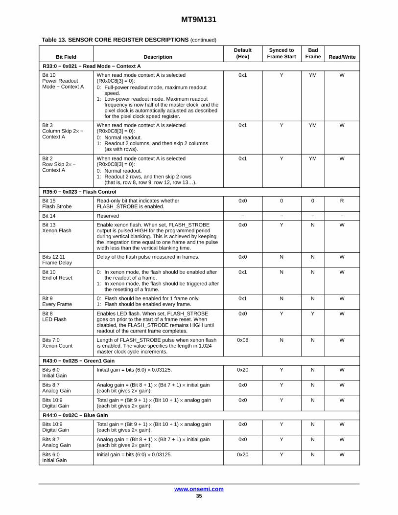
MT9M131
www.onsemi.com35
Table 13. SENSOR CORE REGISTER DESCRIPTIONS (continued)
Bit Field Read/WriteBad
FrameSynced to
Frame StartDefault(Hex)Description
R33:0 − 0x021 − Read Mode − Context A
Bit 10Power ReadoutMode − Context A
When read mode context A is selected (R0x0C8[3] = 0):0: Full-power readout mode, maximum readout
speed.1: Low-power readout mode. Maximum readout
frequency is now half of the master clock, and thepixel clock is automatically adjusted as describedfor the pixel clock speed register.
0x1 Y YM W
Bit 3Column Skip 2× −Context A
When read mode context A is selected (R0x0C8[3] = 0):0: Normal readout.1: Readout 2 columns, and then skip 2 columns
(as with rows).
0x1 Y YM W
Bit 2Row Skip 2× −Context A
When read mode context A is selected (R0x0C8[3] = 0):0: Normal readout.1: Readout 2 rows, and then skip 2 rows
(that is, row 8, row 9, row 12, row 13…).
0x1 Y YM W
R35:0 − 0x023 − Flash Control
Bit 15Flash Strobe
Read-only bit that indicates whetherFLASH_STROBE is enabled.
0x0 0 0 R
Bit 14 Reserved − − − −
Bit 13Xenon Flash
Enable xenon flash. When set, FLASH_STROBEoutput is pulsed HIGH for the programmed periodduring vertical blanking. This is achieved by keepingthe integration time equal to one frame and the pulsewidth less than the vertical blanking time.
0x0 Y N W
Bits 12:11Frame Delay
Delay of the flash pulse measured in frames. 0x0 N N W
Bit 10End of Reset
0: In xenon mode, the flash should be enabled afterthe readout of a frame.
1: In xenon mode, the flash should be triggered afterthe resetting of a frame.
0x1 N N W
Bit 9Every Frame
0: Flash should be enabled for 1 frame only.1: Flash should be enabled every frame.
0x1 N N W
Bit 8LED Flash
Enables LED flash. When set, FLASH_STROBEgoes on prior to the start of a frame reset. Whendisabled, the FLASH_STROBE remains HIGH untilreadout of the current frame completes.
0x0 Y Y W
Bits 7:0Xenon Count
Length of FLASH_STROBE pulse when xenon flashis enabled. The value specifies the length in 1,024master clock cycle increments.
0x08 N N W
R43:0 − 0x02B − Green1 Gain
Bits 6:0Initial Gain
Initial gain = bits (6:0) × 0.03125. 0x20 Y N W
Bits 8:7Analog Gain
Analog gain = (Bit 8 + 1) × (Bit 7 + 1) × initial gain(each bit gives 2× gain).
0x0 Y N W
Bits 10:9Digital Gain
Total gain = (Bit 9 + 1) × (Bit 10 + 1) × analog gain(each bit gives 2× gain).
0x0 Y N W
R44:0 − 0x02C − Blue Gain
Bits 10:9Digital Gain
Total gain = (Bit 9 + 1) × (Bit 10 + 1) × analog gain(each bit gives 2× gain).
0x0 Y N W
Bits 8:7Analog Gain
Analog gain = (Bit 8 + 1) × (Bit 7 + 1) × initial gain(each bit gives 2× gain).
0x0 Y N W
Bits 6:0Initial Gain
Initial gain = bits (6:0) × 0.03125. 0x20 Y N W

MT9M131
www.onsemi.com36
Table 13. SENSOR CORE REGISTER DESCRIPTIONS (continued)
Bit Field Read/WriteBad
FrameSynced to
Frame StartDefault(Hex)Description
R45:0 − 0x02D − Red Gain
Bits 10:9Digital Gain
Total gain = (Bit 9 + 1) × (Bit 10 + 1) × analog gain(each bit gives 2× gain).
0x0 Y N W
Bits 8:7Analog Gain
Analog gain = (Bit 8 + 1) × (Bit 7 + 1) × initial gain(each bit gives 2× gain).
0x0 Y N W
Bits 6:0Initial Gain
Initial gain = bits (6:0) × 0.03125. 0x20 Y N W
R46:0 − 0x02E − Green2 Gain
Bits 10:9Digital Gain
Total gain = (Bit 9 + 1) × (Bit 10 + 1) × analog gainthreshold (each bit gives 2× gain).
0x0 Y N W
Bits 8:7Analog Gain
Analog gain = (Bit 8 + 1) × (Bit 7 + 1) × initial gain(each bit gives 2× gain).
0x0 Y N W
Bits 6:0Initial Gain
Initial gain = bits (6:0) × 0.03125. 0x20 Y N W
R47:0 − 0x02F − Global Gain
Bits 10:0Global Gain
This register can be used to set all 4 gains at once.When read, it returns the value stored in R0x2B.
0x20 Y N W
R200:0 − 0x0C8 − Context Control
Bit 15Restart
Setting this bit causes the sensor to abandon thecurrent frame and start resetting the first row. Samephysical register as R0x00D[1].
0x0 N YM W
Bit 7Xenon Flash Enable
Enable xenon flash. Same physical register asR0x023[13].
0x0 Y N W
Bit 3Read Mode Select
0: Use read mode, context A, R0x021.1: Use read mode, context B, R0x020.Note that bits found only in the read mode context Bregister is always taken from that register.
0x0 Y YM W
Bit 2LED Flash Enable
Enable LED flash. Same physical register asR0x023[8].
0x0 Y Y W
Bit 1Vertical BlankingSelect
0: Use vertical blanking, context A, R0x008.1: Use vertical blanking, context B, R0x006.
0x0 Y YM W
Bit 0Horizontal BlankingSelect
0: Use horizontal blanking, context A, R0x007.1: Use horizontal blanking, context B, R0x005.
0x0 Y YM W
R240:0 − 0x0F0 − Page Map
Bits 2:0Page Map
Page mapping register. Must be kept at “0” to be ableto write to/read from sensor. Used in the SOC toaccess other pages with registers.
0x0 N 0 W
R241:0 − 0x0F1 − Byte-wise Address
Bit 0Byte-wise Address
Special address to perform 8-bit (instead of 16-bit)reads and writes to the sensor. For additionalinformation, see “Two-Wire Serial Interface Sample”and “Appendix A – Serial Bus Description”.
N/A 0 0 0
R255:0 − 0x0FF − Chip Version (R/O)
Bits 15:0 Hardwired value. 0x143A R

MT9M131
www.onsemi.com37
SENSOR READ MODES AND TIMING
This section provides an overview of typical usage modesfor the MT9M131. It focuses on two primaryconfigurations: the first is suitable for low-powerviewfinding, the second for full resolution snapshots. It alsodescribes mechanisms for switching between these modes.
ContextsThe MT9M131 supports hardware-accelerated context
switching. A number of parameters have two copies of theirsetup registers; this allows two contexts to be loaded at anygiven time. These are referred to as context A and context B.Context selection for any single parameter is determined bythe global context control register (GCCR, see R0x2C8).There are copies of this register in each address page. A writeto any one of them has the identical effect. However,a READ from address page 0 only returns the subset bits ofR0xC8 that are specific to the sensor core.
The user can employ contexts for a variety of purposes;thus the generic naming convention. One typical usagemodel is to define context A as viewfinder or preview modeand context B as snapshot mode. The device defaults areconfigured with this in mind. This mechanism enables theuser to have settings for viewfinder and snapshot modesloaded at the same time, and then switch between them witha single write to R0x2C8.
Viewfinder/Preview and Full-Resolution/SnapshotModes
In the MT9M131, the sensor core supports two primaryreadout modes: low-power preview mode andfull-resolution snapshot mode.
Low-Power Preview ModeQSXGA (640 × 512) images are generated at up to 30 fps.
The reduced-size images are generated by skipping pixels in
the sensor, that is, decimation. The key sensor registers thatdefine this mode are read mode context A register (R0x021)and read mode context B register (R0x020). Only certainbits in these registers are context switchable; any bits that donot have multiple contexts are always defined by their valuesin R0x020. Any active sets of these registers are defined bythe state of R0xNC8[3]. On reset, R0xNC8[3] = 0 selectingR0x021; setups specific to preview are defined by thisregister.
Full-Resolution Snapshot ModeSXGA (1280 × 1024) images are generated at up to 15 fps.
This is typically selected by setting R0x0C8[3] = 1 selectingR0x020 (context B) as the primary read mode register.
Switching ModesTypically, switching to full-resolution or snapshot mode
is achieved by writing R0x2C8 = 0x9F0B. This restarts thesensor and sets most contexts to context B. Following thiswrite, a READ from R0x1C8 or R0x2C8 results in 0x1F0Bbeing read. Note that the most significant bit (MSB) iscleared automatically by the sensor. A READ from R0x0C8results in 0x000B, as only the lower 4 bits and the restartMSB are implemented in the sensor core.
ClocksThe sensor core is a master in the system. The sensor core
frame rate defines the overall image flow pipeline framerate. Horizontal and vertical blanking are influenced by thesensor configuration, and are also a function of certain IFPfunctions − particularly resize. The relationship of theprimary clocks are depicted in Figure 10.
Figure 10. Primary Sensor Core Clock Relationships
SensorMaster Clock
SensorPixel Clock
Sensor CoreDiv by 2
Div by N
Colorpipe
Output FIFO
10 bits/pixel1 pixel/clock
16 bits/pixel1 pixel/clock
16 bits/pixel0.5 pixel/clock
EXTCLK

MT9M131
www.onsemi.com38
The IFP typically generates up to 16 bits per pixel, forexample YCbCr or 565RGB, but has only an 8-bit portthrough which to communicate this pixel data. There is nophase locked loop (PLL), so the primary input clock(EXTCLK) must be twice the fundamental pixel rate(defined by the sensor pixel clock).
To generate SXGA images at 15 fps, the sensor corerequires a clock in the 24 to 27 MHz range; this is also thefundamental pixel clock rate (sensor pixel clock) forfull-power operation. To achieve this pixel rate, EXTCLKmust be in the 48 to 54 MHz range. The device defaultsassume a 54 MHz clock. Minimum clock frequency is2 MHz.
Primary Operating ModesThe MT9M131 supports two primary modes of operation
with respect to the sensor core that affect pixel rate, framerate, and blanking.
Full-Power Readout ModeThe sensor is in full resolution mode, generating
1.3 megapixels (SXGA = 1,280 × 1,024 + border) forinterpolation. The SXGA image fed from the sensor to thecolorpipe can be resized in the colorpipe, but the frame rateis still defined by sensor core operation. In full-powerreadout mode, with full FOV, the frame rate is invariant withthe final image size:
Context Typically Context B
Sensor Read Mode Settings
No SkippingFull-power Readout, that is, FullData Rate
Sensor Pixel Clock 27 MHz for 54 MHz Master Clock:Maximum Pixel Rate of27 Megapixels per Second
Maximum Frame Rate For 54 MHz Master Clock, 15 fps
Low-Power Readout ModeRunning under low-power readout, the sensor is in skip
mode, and generates QSXGA frames (640 × 512 + border =336,960 pixels). This full FOV QSXGA image can beresized, but only to resolutions smaller than QSXGA.The frame rate is defined by the operating mode of thesensor:
Context Typically Context A
Sensor Read Mode Settings
Row Skip 2×Column Skip 2×Low-power Readout Maximum DataRate is Half that of Full-powerReadout
Sensor Pixel Clock 13.5 MHz for 54 MHz Master Clock:Maximum Pixel Rate of13.5 Megapixels per Second
Maximum Frame Rate For 54 MHz Master Clock, 30 fps
Tuning Frame RatesActual frame rates can be tuned by adjusting various
sensor parameters. The sensor registers are in page 0, thusthe “0” at the beginning of each register address:
Table 14. REGISTER ADDRESS FUNCTIONS
Register Function
R0x004 Window width, typically 1280 in the MT9M131
R0x003 Window height, typically 1024 in the MT9M131
LOW-POWER READOUT MODE − CONTEXT A
R0x007 Horizontal blanking, default is 190 (units of sensor pixel clocks)
R0x008 Vertical blanking, default is 17 (rows including black rows)
FULL-POWER READOUT MODE − CONTEXT B
R0x005 Horizontal blanking, default is 388 (units of sensor pixel clocks)
R0x006 Vertical blanking, default is 42 (rows including black rows)
In the MT9M131, the sensor core adds 4 border pixels allthe way around the image, taking the active image size to1288 × 1032 in full-power snapshot resolution, and648 × 520 when skipping rows in low-power previewresolution. This is achieved through the default settings:• Read mode context B: R0x020
• Oversize and show border bits are set by default
• Oversize and show border bits are not contextswitchable, thus their location only in read modecontext B
Default Blanking CalculationsThe MT9M131 default blanking calculations are
a function of context, as follows:
[REG<a> | REG<b>]:• Reg<a>
Low-power readout = context A, typically used forviewfinder
• Reg<b>Full power readout = context B, typically used forsnapshots

MT9M131
www.onsemi.com39
Table 15. BLANKING PARAMETER CALCULATIONS
Parameter Calculation
PC_PERIODSensor Pixel Clock Period
Full-power Readout: (2/54) �s = 0.0370 �sLow-power Readout: (4/54) �s = 0.0185 �s
A: Active Data Time (per line):R0x004 + 8 (border) × PC_PERIOD
Full-power Readout: A = 1,288 × (2/54) �s = 47.704 �sLow-power Readout: A = 648 × (4/54) �s = 48.000 �s
Q: Horizontal Blanking:[R0x005 | R0x007] × PC_PERIOD
Full-power Readout: Q = 388 × (2/54) �s = 14.370 �sLow-power Readout: Q = 190 × (4/54) �s = 14.074 �s
Row Time = Q + A: Full-power Readout: 62.074 �sLow-power Readout: 62.074 �s
P: Frame Start/End Blanking:4 × PC_PERIOD
Full-power Readout: P = 4 × (2/54) �s = 0.148 �sLow-power Readout: P = 4 × (4/54) �s = 0.296 �s
V: Vertical Blanking:[R0x006 | R0x008] × (Q + A) + (Q − 2 × P)
Full-power Readout: V = (42 × 62.074) + (14.370 − 0.296) = 2,621.333 �sLow-power Readout: V = (17 × 62.074) + (14.074 − 0.593) = 1,068.740 �s
F: Total Frame Time:(R0x003 + [R0x006 | R00x008]) × (Q + A)
Full-power Readout: F = (1,032 + 42) × 62.074 �s = 66,667.556 �s ≥ 15 fpsLow-power Readout: F = (520 + 17) × 62.074 �s = 33,333.778 �s ≥ 30 fps
NOTE: The line rate (row rate) is the same for both low power and full power readout modes. This ensures that when switching modes,exposure time does not change; the pre-existing shutter width remains valid.
User Blanking CalculationsWhen calculating blanking for different clock rates,
minimum values for horizontal blanking and verticalblanking must be taken into account. Table 16 showsminimum values for each register.
Table 16. USER BLANKING MINIMUM VALUES
Parameter Register Minimum
Horizontal Blanking Full-power Readout (Context B): R0x005Low-power Readout (Context A): R0x007
202 (Sensor Pixel Clocks)114 (Sensor Pixel Clocks)
Vertical Blanking Full-power Readout (Context B): R0x006Low-power Readout (Context A): R0x008
5 (Rows)5 (Rows)
Exposure and Sensor Context SwitchingThe MT9M131 incorporates device setup features that
prevent changes in sensor context from causing a change inexposure when switching between preview/viewfinder andfull resolution/snapshot modes. This is achieved by keepingthe line rate consistent between modes.
ExposureDefined by the shutter width. This is the number of lines
to be reset before starting a frame read. If line rate does notchange when a mode changes, exposure does not change.
Switching From Context A to Context BUnder typical/default settings, the sensor pixel rate
doubles when switching from preview (context A) to fullresolution (context B). Additionally, the number of pixels tobe read per line nearly doubles. This naturally keeps the linerates roughly equal. The difference occurs due to borderpixels: for SOC operation, there are always 8 border pixelsregardless of context, thus the number of pixels in each lineis not quite doubled.
Horizontal BlankingDefined in terms of sensor pixel clocks. The sensor pixel
clock rate doubles when switching from low-power readout
mode (preview context A) to full-power readout mode (fullresolution context B). To maintain the same horizontalblanking time, the value for horizontal blanking mustdouble. This is handled by the dual, context-switchablehorizontal blanking registers.
Switching ModesInitiate mode switches from preview (context A) to
snapshot (context B) during vertical blanking; switchingshould be accompanied by a sensor restart. Ensure thatR0x0C8[15] is written as “1” when changing contexts.
Switching FrequencyThe user can switch between sensor contexts as frequently
as necessary (without affecting exposure) constant switchescan occur as often as once per frame.
Simple SnapshotsTo take a snapshot, simply switch from context A to
context B (with restart) for a few frames, then switch backagain, capturing one of the context B frames as the snapshot.Alternative methods are supported by an internal sequencer.These additional methods are advantageous for taking flashsnapshots.

MT9M131
www.onsemi.com40
Output Timing
Figure 11. Vertical Timing
ÉÉ
ÉÉÉÉÉÉÉÉÉÉ
ÉÉÉÉ
ÉÉ
ÉÉÉÉ
ÉÉ
ÉÉÉÉÉÉÉÉÉÉÉÉÉÉ
ÉÉÉÉLine 0 Line 1 LineN−3 LineN−2 LineN−1 Line 0
FRAME_VALID
LINE_VALID
D[7:0]
E F
D BCA
ÉÉÉÉ
NO DATA
Figure 12. Horizontal Timing
10 FF 00 00 80 CB0 Y0 CR1 Y1 CB3 Y3 CRn−1
Yn FF 00 00 9D
PIXCLK
LINE_VALID
D[7:0] 10
Notes:1. Line start: FF00 0080.2. Line end: FF00 009D.
Typical Resolutions, Modes, and TimingThe parameters in Table 17 are illustrated in waveform
diagram Figure 11. Table 22 provides values for theseparameters in some common resolutions and operatingmodes.
Table 17. BLANKING DEFINITIONS
Designation Definition
A FV (Rising Edge) to LV (Rising Edge) Delay
B LV (Falling Edge) to FV (Falling Edge) Delay
C LV (HIGH/Valid) Time
D LV (LOW/Horizontal Blanking) Time
E FV (HIGH/Valid) Time
F FV (LOW/Vertical Blanking) Time
(G) Number of PIXCLK Cycles in a Given Burst
(H) Number of PIXCLK Cycles between Bursts
Reset, Clocks, and Standby
Functional OperationPower-up reset is asserted/de-asserted on RESET_BAR.
It is active LOW. In this reset state, all control registers havethe default values. All internal clocks are turned off exceptfor the divided-by-2 clock to the sensor core.
Soft reset is asserted/de-asserted by the two-wire serialinterface program. There are sensor core soft resets and SOCsoft resets. In soft reset mode, the two-wire serial interfaceand register ring bus are still running. All control registersare reset using default values. See R0x00D.
Hard standby is asserted/de-asserted on STANDBY. It isactive HIGH. In this hard standby state, all internal clocksare turned off and analog block is in standby mode to savepower consumption.
NOTE: Following the assertion of hard standby, at least24 master clock cycles must be delivered tocomplete the transition to the hard standby state.
Soft standby is asserted/de−asserted differently in thesensor page or colorpipe page. The sensor soft standby bit isin R0x00D[2]. Colorpipe soft standby disables some of the

MT9M131
www.onsemi.com41
SOC clocks, including the pixel clock. This bit isR0x1B3[0]. The colorpipe must first be brought out ofstandby through R0x1B3[0].
The colorpipe soft standby is provided to enable the userto turn off the colorpipe and the sensor independently.
By default, all outputs except SDATA are disabled duringhard standby. This feature can be disabled by setting
R0x1B3[1] = 0. Independent control of the outputs isavailable either through OE_BAR or R0x00D[4]. Alloutputs are implemented using bidirectional buffers, thusshould not be left tri-stated. In dual camera applications,ensure that one camera is driving the bus, or that the bus ispulled to VGNDIO or VDDIO, even during standby.
ELECTRICAL SPECIFICATIONS
Table 18. ELECTRICAL CHARACTERISTICS AND OPERATING CONDITIONS (TA = Ambient = 25°C)
Parameter Condition Min Typ Max Unit
I/O Digital Voltage (VDD_IO) 1.8 – 3.1 V
Core Digital Voltage (VDD) 2.5 2.8 3.1 V
Analog Voltage (VAA) 2.5 2.8 3.1 V
Pixel Supply Voltage (VAA_PIX) 2.5 2.8 3.1 V
Leakage Current STANDBY, No Clocks – – 10 �A
Operating Temperature Measured at Junction –30 – +70 °C
NOTE: VDD, VAA, and VAAPIX must all be at the same potential to avoid excessive current draw. Care must be taken to avoid excessive noiseinjection in the analog supplies if all three supplies are tied together.
Table 19. I/O PARAMETERS
Signal Parameter Definitions Condition Min Typ Max Unit
All Outputs Load Capacitance – – 30 pF
Output Pin Slew 2.8 V, 30 pF Load – 0.72 – V/ns
2.8 V, 5 pF Load – 1.25 – V/ns
1.8 V, 30 pF Load – 0.34 – V/ns
1.8 V, 5 pF Load – 0.51 – V/ns
VOH Output HIGH Voltage VDD_IO – 0.3 – VDD_IO V
VOL Output LOW Voltage 0 – 0.3 V
IOH Output HIGH Current VDD_IO = 2.8 V, VOH = 2.4 V
16 – 26.5 mA
VDD_IO = 1.8 V, VOH = 1.4 V
8 – 15 mA
IOL Output LOW Current VDD_IO = 2.8 V,VOL = 0.4 V
15.9 – 21.3 mA
VDD_IO = 1.8 V, VOL = 0.4 V
10.1 – 16.2 mA
IOZ Tri-state OutputLeakage Current
– – 10 �A
All Inputs VIH Input HIGH Voltage VDD_IO = 2.8 V 2.0 – – V
VDD_IO = 1.8 V 1.2 – – V
VIL Input LOW Voltage VDD_IO = 2.8 V – – 0.9 V
VDD_IO = 1.8 V – – 0.6 V
IIN Input Leakage Current –5 – +5 �A
PIN CAP Ball Input Capacitance – 3.5 – pF
EXTCLK Freq Master ClockFrequency
Absolute Minimum 2 – – MHz
SXGA at 15 fps 48 – 54 MHz

MT9M131
www.onsemi.com42
Table 20. ABSOLUTE MAXIMUM RATINGS
Symbol Parameter Min Max Unit
VSUPPLY Power Supply Voltage (All Supplies) –0.3 4.0 V
ISUPPLY Total Power Supply Current 150 mA
IGND Total Ground Current 150 mA
VIN DC Input Voltage –0.3 VDD_IO + 0.3 V
VOUT DC Output Voltage –0.3 VDD_IO + 0.3 V
TSTG Storage Temperature –40 85 °C
Stresses exceeding those listed in the Maximum Ratings table may damage the device. If any of these limits are exceeded, device functionalityshould not be assumed, damage may occur and reliability may be affected.
Power Consumption
Table 21. POWER CONSUMPTION AT 2.8 V
Mode SensorImage FlowProcessor
I/Os(10 pF)
Total PowerConsumption Unit
SXGA at 15 fps 90 71 9 170 mW
QSXGA at 30 fps 50 36 4 90 mW
QSXGA at 15 fps 50 18 2 70 mW
QVGA at 30 fps 50 32 1 83 mW
I/O TimingBy default, the MT9M131 launches pixel data, FV, and LV
synchronously with the falling edge of PIXCLK. This is
reflected by the default setting of R0x13A[9] andR0x19B[9] = 1. The expectation is that the user capturesDOUT, FV, and LV using the rising edge of PIXCLK.
Figure 13. AC Output Timing Diagram
EXTCLK
PIXCLK
FV
LV
DOUT[7:0]
tPHLp
tPLHp
tR tF
PtFVSETUP
tLVSETUP
tDSETUP tDHOLD
DOUT[7:0] DOUT[7:0]
tPIXCLK_HIGH tPIXCLK_LOW
tEXTCLK_HIGH tEXTCLK_LOW

MT9M131
www.onsemi.com43
Table 22. AC OUTPUT TIMING DATA (TA = +25°C, VAA = VAA_PIX = VDD = VDD_IO = 2.8 V)
Parameter Description Min Typ Max Unit
fEXTCLK Input Clock Frequency – – 54 MHz
tEXTCLK_HIGH Input Clock (EXTCLK) HIGH Time 40 50 60 %
tEXTCLK_LOW Input Clock (EXTCLK) LOW Time 40 50 60 %
tR EXTCLK Rise Time – 4.5 8 ns
tF EXTCLK Fall Time – 4.5 8 ns
tR DOUT Data Out Rise Time – 4.5 9 ns
tF DOUT Data Out Fall Time – 4.5 9 ns
tPHLP Propagation Delay from CLK HIGH to PIXCLK LOW 7 9 15 ns
tPLHP Propagation Delay from CLK LOW to PIXCLK HIGH 7 9 15 ns
tPIXCLK_HIGH Pixel Clock HIGH Time 40 50 60 %
tPIXCLK_LOW Pixel Clock LOW Time 40 50 60 %
tFVSETUP Frame Valid Setup Time 4 8 P ns
tLVSETUP Line Valid Setup Time 4 8 P ns
tDSETUP Data Out Setup Time 4 8 P ns
tDHOLD Data Out Hold Time 4 8 P ns
1. FV, LV, PIXCLK ,and DOUT are referenced from EXTCLK and, therefore, have the same propagation delay with respect to EXTCLK.2. P = (1/2) PIXCLK Period.3. Minimum and maximum (rise and fall) times for EXTCLK and DOUT will depend on the type of input signal and load capacitance.
Figure 14. Spectral Response Chart
Wavelength (nm)
350
Qu
antu
m E
ffic
ien
cy (
%)
450 550 650 750 850 950 10500
5
10
15
20
25
30
35
40
45

MT9M131
www.onsemi.com44
CRA vs. Image Height Plot
Image Height CRA
(%) (mm) (deg)C
hie
f R
ay A
ng
le (
Deg
)
Image Height (%)
MT9M131 CRA Characteristic
0 10 20 30 40 50 60 70 80 90 100 110
0
2
4
6
8
10
12
14
16
18
20
Figure 15. Chief Ray Angle vs. Image Height
22
24
26
0 0 0
5 0.148 1.28
10 0.295 2.56
15 0.443 3.84
20 0.590 5.12
25 0.738 6.40
30 0.885 7.68
35 1.033 8.96
40 1.180 10.25
45 1.328 11.53
50 1.475 12.81
55 1.623 14.09
60 1.770 15.37
65 1.918 16.65
70 2.065 17.93
75 2.213 19.21
80 2.360 20.49
85 2.508 21.77
90 2.656 23.05
95 2.803 24.33
100 2.951 25.61
Figure 16. Optical Center Diagram
− Direction + Direction
−37.66 �m
+15.63 �m
− Direction
+ Direction
Die Center(0 �m, 0 �m)
First Clear Pixel(26, 8)
Last Clear Pixel(1314, 1040)
Optical CenterNOTE: Figure not to scale.

MT9M131
www.onsemi.com45
Appendix A − Serial Bus Description
Registers are written to and read from the MT9M131through the two-wire serial interface bus. The sensor isa serial interface slave and is controlled by the serial clock(SCLK). SCLK is driven by the serial interface master. Datais transferred into and out of the MT9M131 through theserial data (SDATA) line. The SDATA line is pulled up toVDD_IO off-chip by a 1.5 k� resistor. Either the slave or themaster device can pull the SDATA line down − the two-wireserial interface protocol determines which device is allowedto pull the SDATA line down at any given time.
ProtocolThe two-wire serial interface defines several different
transmission codes, as shown in the following sequence:1. A start bit.2. The slave device 8-bit address. The SADDR pin is
used to select between two different addresses incase of conflict with another device. If SADDR isLOW, the slave address is 0x90; if SADDR isHIGH, the slave address is 0xBA.
3. An (a no) acknowledge bit.4. An 8-bit message.5. A stop bit.
SequenceA typical READ or WRITE sequence is executed as
follows:1. The master sends a start bit.2. The master sends the 8-bit slave device address.
The last bit of the address determines if the requestis a READ or a WRITE, where a “0” indicatesa WRITE and a “1” indicates a READ.
3. The slave device acknowledges receipt of theaddress by sending an acknowledge bit to themaster.
4. If the request is a WRITE, the master thentransfers the 8-bit register address, indicatingwhere the WRITE takes place.
5. The slave sends an acknowledge bit, indicatingthat the register address has been received.
6. The master then transfers the data, 8 bits at a time,with the slave sending an acknowledge bit aftereach 8 bits.
The MT9M131 uses 16-bit data for its internal registers,thus requiring two 8-bit transfers to write to one register.After 16 bits are transferred, the register address isautomatically incremented so that the next 16 bits arewritten to the next register address. The master stops writingby sending a start or stop bit.
A typical READ sequence is executed as follows.1. The master sends the write-mode slave address
and 8-bit register address, just as in the writerequest.
2. The master then sends a start bit and theread-mode slave address, and clocks out theregister data, 8 bits at a time.
3. The master sends an acknowledge bit after each8-bit transfer. The register address is automaticallyincremented after every 16 bits is transferred.
4. The data transfer is stopped when the master sendsa no-acknowledge bit.
Bus Idle StateThe bus is idle when both the data and clock lines are
HIGH. Control of the bus is initiated with a start bit, and thebus is released with a stop bit. Only the master can generatethe start and stop bits.
Start BitThe start bit is defined as a HIGH-to-LOW transition of
the data line while the clock line is HIGH.
Stop BitThe stop bit is defined as a LOW-to-HIGH transition of
the data line while the clock line is HIGH.
Slave AddressThe 8-bit address of a two-wire serial interface device
consists of seven bits of address and 1 bit of direction. A “0”in the least significant bit (LSB) of the address indicateswrite mode, and a “1” indicates read mode. The writeaddress of the sensor is 0xBA; the read address is 0xBB. Thisapplies only when the SADDR is set HIGH.
Data Bit TransferOne data bit is transferred during each clock pulse.
The serial interface clock pulse is provided by the master.The data must be stable during the HIGH period of thetwo-wire serial interface clock − it can only change when theserial clock is LOW. Data is transferred 8 bits at a time,followed by an acknowledge bit.
Acknowledge BitThe master generates the acknowledge clock pulse.
The transmitter (which is the master when writing, or theslave when reading) releases the data line, and the receiversignals an acknowledge bit by pulling the data line LOWduring the acknowledge clock pulse.
No-Acknowledge BitThe no-acknowledge bit is generated when the data line is
not pulled down by the receiver during the acknowledgeclock pulse. A no-acknowledge bit is used to terminatea read sequence.

MT9M131
www.onsemi.com46
Two-Wire Serial Interface Sample
WRITE and READ Sequences (SADDR = 1)
16-Bit WRITE SequenceA typical WRITE sequence for writing 16 bits to a register
is shown in Figure 17. A start bit sent by the master starts thesequence, followed by the write address. The image sensorsends an acknowledge bit and expects the register address to
come first, followed by the 16-bit data. After each 8-bittransfer, the image sensor sends an acknowledge bit. All 16bits must be written before the register is updated. After 16bits are transferred, the register address is automaticallyincremented so that the next 16 bits are written to the nextregister. The master stops writing by sending a start or stopbit.
Figure 17. WRITE Timing to R0x009 − Value 0x0284
0xBA Address
Start Stop
ACK ACK ACK ACK
R0x09 0000 0010 1000 0100
SCLK
SDATA
16-Bit READ SequenceA typical READ sequence is shown in Figure 18. The
master writes the register address, as in a WRITE sequence.Then a start bit and the read address specify that a read isabout to occur from the register. The master then clocks out
the register data, 8 bits at a time. The master sends anacknowledge bit after each 8-bit transfer. The registeraddress should be incremented after every 16 bits istransferred. The data transfer is stopped when the mastersends a no-acknowledge bit.
Figure 18. READ Timing from R0x009; Returned Value 0x0284
0xBA Address
Start Start Stop
ACK ACK ACK ACK NACK
R0x09 0xBB Address 0000 0010 1000 0100
SCLK
SDATA
8-Bit WRITE SequenceTo be able to write one byte at a time to the register,
a special register address is added. The 8-bit WRITE isstarted by writing the upper 8 bits to the desired register, thenwriting the lower 8 bits to the special register address
(R0x0F1). The register is not updated until all 16 bits havebeen written. It is not possible to update just half of a register.Figure 19 shows a typical sequence for an 8-bit WRITE.The second byte is written to the special register (R0x0F1).
Figure 19. WRITE Timing to R0x009 − Value 0x0284
0xBA Address
Start StopACK ACK ACK ACK
R0x09 0xBA Address
StartACKACK
R0xF10000 0010 1000 0100
SCLK
SDATA
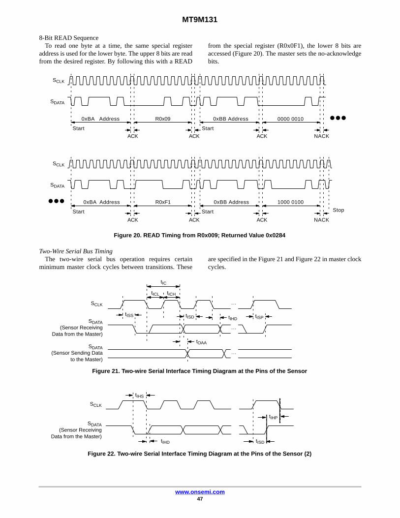
MT9M131
www.onsemi.com47
8-Bit READ SequenceTo read one byte at a time, the same special register
address is used for the lower byte. The upper 8 bits are readfrom the desired register. By following this with a READ
from the special register (R0x0F1), the lower 8 bits areaccessed (Figure 20). The master sets the no-acknowledgebits.
Figure 20. READ Timing from R0x009; Returned Value 0x0284
0xBA Address
Start Start
NACK
R0x09 0xBB Address 0000 0010
0xBA Address
Start Start Stop
NACK
R0xF1 0xBB Address 1000 0100���
���
ACK
SCLK
SDATA
ACK ACK
ACK ACK ACK
SCLK
SDATA
Two-Wire Serial Bus TimingThe two-wire serial bus operation requires certain
minimum master clock cycles between transitions. Theseare specified in the Figure 21 and Figure 22 in master clockcycles.
Figure 21. Two-wire Serial Interface Timing Diagram at the Pins of the Sensor
tISPtIHDtISD
tOAA
tISS
tICL tICH
tIC
…
…
…
SCLK
SDATA(Sensor Receiving
Data from the Master)
SDATA(Sensor Sending Data
to the Master)
Figure 22. Two-wire Serial Interface Timing Diagram at the Pins of the Sensor (2)
tIHS
SDATA(Sensor Receiving
Data from the Master)
SCLK
tIHD tISD
tIHP

MT9M131
www.onsemi.com48
Table 23. TWO-WIRE SERIAL INTERFACE TIMING (VDD = VAA = VAA_PIX = VDD_IO = 2.8 V, TA = −30°C to +70°C)
Symbol Definition Min Typ Max Unit
fIC Two-wire Serial Bus Input Clock Frequency – – 400 KHz
tIC Two-wire Serial Bus Input Clock Period 2500 – – ns
tICL Two-wire Serial Bus Clock LOW – 1250 – ns
tICH Two-wire Serial Bus Clock HIGH – 1250 – ns
tISS Setup Time for Start Condition 600 – – ns
tIHS Hold Time for Start Condition 600 – – ns
tISD Setup Time for Input Data 600 – – ns
tIHD Hold Time for Input Data 600 – – ns
tOAA Output Delay Time – – 600 ns
tISP Setup Time of Stop Condition 600 – – ns
tIHP Hold Time for Stop Condition 600 – – ns
CSCLCK/SDATA SCLCK and SDATA Load Capacitance – – 30 pF
RSCLCK/SDATA SCLCK and SDATA Pull-up Resistor – 1.5 – k�
NOTE: A minimum EXTCLK frequency of 4 MHz is required for the two-wire serial interface to operate at 400 kHz.

XXXX = Specific Device CodeY = YearZZZ = Lot Traceability
*This information is generic. Please refer todevice data sheet for actual part marking.Pb−Free indicator, “G” or microdot “�”, mayor may not be present. Some products maynot follow the Generic Marking.
GENERICMARKING DIAGRAM*
CLCC48 11.43x11.43CASE 848AV
ISSUE ADATE 21 OCT 2019
MECHANICAL CASE OUTLINE
PACKAGE DIMENSIONS
ON Semiconductor and are trademarks of Semiconductor Components Industries, LLC dba ON Semiconductor or its subsidiaries in the United States and/or other countries.ON Semiconductor reserves the right to make changes without further notice to any products herein. ON Semiconductor makes no warranty, representation or guarantee regardingthe suitability of its products for any particular purpose, nor does ON Semiconductor assume any liability arising out of the application or use of any product or circuit, and specificallydisclaims any and all liability, including without limitation special, consequential or incidental damages. ON Semiconductor does not convey any license under its patent rights nor therights of others.
98AON94065FDOCUMENT NUMBER:
DESCRIPTION:
Electronic versions are uncontrolled except when accessed directly from the Document Repository.Printed versions are uncontrolled except when stamped “CONTROLLED COPY” in red.
PAGE 1 OF 1CLCC48 11.43x11.43
© Semiconductor Components Industries, LLC, 2018 www.onsemi.com

onsemi, , and other names, marks, and brands are registered and/or common law trademarks of Semiconductor Components Industries, LLC dba “onsemi” or its affiliatesand/or subsidiaries in the United States and/or other countries. onsemi owns the rights to a number of patents, trademarks, copyrights, trade secrets, and other intellectual property.A listing of onsemi’s product/patent coverage may be accessed at www.onsemi.com/site/pdf/Patent−Marking.pdf. onsemi reserves the right to make changes at any time to anyproducts or information herein, without notice. The information herein is provided “as−is” and onsemi makes no warranty, representation or guarantee regarding the accuracy of theinformation, product features, availability, functionality, or suitability of its products for any particular purpose, nor does onsemi assume any liability arising out of the application or useof any product or circuit, and specifically disclaims any and all liability, including without limitation special, consequential or incidental damages. Buyer is responsible for its productsand applications using onsemi products, including compliance with all laws, regulations and safety requirements or standards, regardless of any support or applications informationprovided by onsemi. “Typical” parameters which may be provided in onsemi data sheets and/or specifications can and do vary in different applications and actual performance mayvary over time. All operating parameters, including “Typicals” must be validated for each customer application by customer’s technical experts. onsemi does not convey any licenseunder any of its intellectual property rights nor the rights of others. onsemi products are not designed, intended, or authorized for use as a critical component in life support systemsor any FDA Class 3 medical devices or medical devices with a same or similar classification in a foreign jurisdiction or any devices intended for implantation in the human body. ShouldBuyer purchase or use onsemi products for any such unintended or unauthorized application, Buyer shall indemnify and hold onsemi and its officers, employees, subsidiaries, affiliates,and distributors harmless against all claims, costs, damages, and expenses, and reasonable attorney fees arising out of, directly or indirectly, any claim of personal injury or deathassociated with such unintended or unauthorized use, even if such claim alleges that onsemi was negligent regarding the design or manufacture of the part. onsemi is an EqualOpportunity/Affirmative Action Employer. This literature is subject to all applicable copyright laws and is not for resale in any manner.
PUBLICATION ORDERING INFORMATIONTECHNICAL SUPPORTNorth American Technical Support:Voice Mail: 1 800−282−9855 Toll Free USA/CanadaPhone: 011 421 33 790 2910
LITERATURE FULFILLMENT:Email Requests to: [email protected]
onsemi Website: www.onsemi.com
Europe, Middle East and Africa Technical Support:Phone: 00421 33 790 2910For additional information, please contact your local Sales Representative
◊