z8820 pxie dc power & digital io controller · 2017-01-24 · z8820 pxie dc power & digital...
TRANSCRIPT

© 2016 LitePoint, A Teradyne Company. All rights reserved.
TECHNICAL SPECIFICATIONS
z8820 PXIeDC Power & Digital IO Controller

z8820 PXIe DC Power & Digital IO Controller 2
OverviewThe z8820 PXIe DC Power & Digital IO Controller Module is a single-slot 3U PXIe module that supports remote instrumentation modules outside the PXI chassis such as the z8812 Port Module. The z8820 module uses a PCI Express (PCIe) Gen1 x1 lane to interface to the PXIe host computer. PCIe read/write operations provide access to the z8820 on-board resources and to digital I/O or SPI interfaces to remote instruments. The z8820 PXIe module supports up to two remote instrument interfaces via two D-sub 26-pin connectors. Each remote channel connector provides eight digital I/O (DIO) signals and three power supply rails (+6V, +9V, and -13V) for external modules. The external power supply rails have voltage/current monitors that can also be used as over/under trip protection. The z8820 also has a programmable clock generator circuit to provide up to three programmable digital clocks for the SPI master circuit and for user signals on the DIO or backplane outputs.
Figure 1: Block Diagram of z8820 PXIe Module
PXIe XJ3-4 DB-26H (x2)
SMPS+6V @ 3A total+12VI
+3.3VI
PXIe GEN1 DIO1-8
DIR1-8
CTLR
CTLR
CTLR
CTLR V-IMeasure
V-IMeasure
V-IMeasure
ClockGenerator
Buffer
EEPROM
25 MHz
CLK GEN1-3
CTLR
CLK100
CLK10
GA
PXI TRG0-7
PXI STAR
+9V @ 1.5A total
-13V @ 1A total
SMPS
SMPS
SMPS
LDO
FPGA

z8820 PXIe DC Power & Digital IO Controller 3
Port Descriptions
Front Panel
Label Type Description
Channel 1 DB-26H DC power supplies and digital IO control bus #1
Channel 2 DB-26H DC power supplies and digital IO control bus #2
The z8820 PXIe uses two D-sub 26-pin triple row connectors for Channel 1 and Channel 2 interfaces. D-sub mating cables can be from 1 foot to 15 feet in length (example mating cable P/N: L-com CHD26MF).
Connector PinoutFor both channels, the pinout of the D-sub 26-pin triple row connector is identical and is shown in the following figure and table.
Figure 2: Front Panel of z8820 DC Power & Digital IO PXIe Module
Figure 3: Front Panel Connector Pinout Diagram
+6V
GND
J1
GND
GND
GND
GND
19
20
21
22
23
24
25
26
10
27
285748481-5
11
12
13
14
15
16
17
18
1
2
3
4
5
6
7
8
9
+9V
-13V
+6V
DIO7
DIO8
DIO5
DIO6
DIO3
DIO4
DIO1
DIO2
+9V
-13V
z8820 PXIe DC Power & Digital IO Controller 4
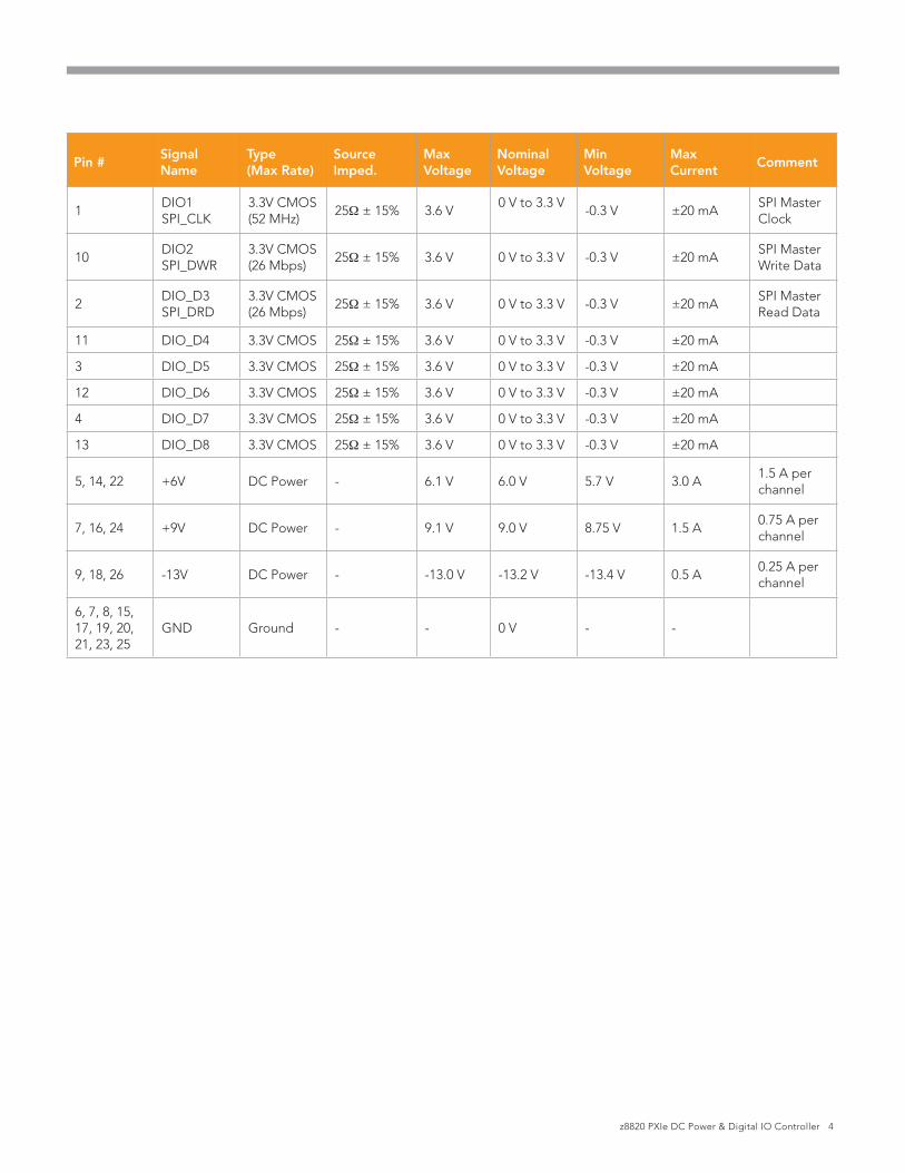
Pin # SignalName
Type(Max Rate)
Source Imped.
MaxVoltage
NominalVoltage
MinVoltage
Max Current Comment
1DIO1SPI_CLK
3.3V CMOS (52 MHz)
25Ω ± 15% 3.6 V0 V to 3.3 V
-0.3 V ±20 mASPI Master Clock
10DIO2SPI_DWR
3.3V CMOS(26 Mbps)
25Ω ± 15% 3.6 V 0 V to 3.3 V -0.3 V ±20 mASPI Master Write Data
2DIO_D3SPI_DRD
3.3V CMOS(26 Mbps)
25Ω ± 15% 3.6 V 0 V to 3.3 V -0.3 V ±20 mASPI Master Read Data
11 DIO_D4 3.3V CMOS 25Ω ± 15% 3.6 V 0 V to 3.3 V -0.3 V ±20 mA
3 DIO_D5 3.3V CMOS 25Ω ± 15% 3.6 V 0 V to 3.3 V -0.3 V ±20 mA
12 DIO_D6 3.3V CMOS 25Ω ± 15% 3.6 V 0 V to 3.3 V -0.3 V ±20 mA
4 DIO_D7 3.3V CMOS 25Ω ± 15% 3.6 V 0 V to 3.3 V -0.3 V ±20 mA
13 DIO_D8 3.3V CMOS 25Ω ± 15% 3.6 V 0 V to 3.3 V -0.3 V ±20 mA
5, 14, 22 +6V DC Power - 6.1 V 6.0 V 5.7 V 3.0 A1.5 A per channel
7, 16, 24 +9V DC Power - 9.1 V 9.0 V 8.75 V 1.5 A0.75 A per channel
9, 18, 26 -13V DC Power - -13.0 V -13.2 V -13.4 V 0.5 A0.25 A per channel
6, 7, 8, 15, 17, 19, 20, 21, 23, 25
GND Ground - - 0 V - -
z8820 PXIe DC Power & Digital IO Controller 5
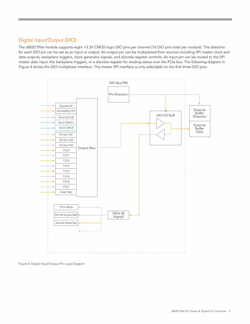
Digital Input/Output (DIO)The z8820 PXIe module supports eight +3.3V CMOS logic DIO pins per channel (16 DIO pins total per module). The direction for each DIO pin can be set as an input or output. An output pin can be multiplexed from sources including SPI master clock and data outputs, backplane triggers, clock generator signals, and discrete register controls. An input pin can be routed to the SPI master data input, the backplane triggers, or a discrete register for reading status over the PCIe bus. The following diagram in Figure 4 shows the DIO multiplexer interface. The master SPI interface is only selectable on the first three DIO pins.
Figure 4: Digital Input/Output Pin Logic Diagram
ExternalBuffer
DirectionDIO I/O Buff.
DIO Bus PIN
DIOx IN(signal)
Output Mux
Discrete IN*
DiscreteReg OUT
Serial SCLK [0]
Serial DWR [1]
Serial CS# [3]
Clk Gen Clk1
Clk Gen Clk2
Clk Gen Clk3
TTLT0
TTLT1
TTLT2
TTLT3
TTLT4
TTLT5
TTLT6
TTLT7
STAR TRIG
TTLTn MUXs
DIO SPI Engine DRD
Discrete Ready Reg
Pin Direction
ExternalBufferData

z8820 PXIe DC Power & Digital IO Controller 6
Item Description Minimum Typical Maximum Units
VImax Voltage – In -0.3 3.6 V
VOmax Voltage – Output 0.0 3.3 V
VIH Voltage – High-level Input 2.0 V
VIL Voltage – Low-level Input 0.8 V
VOH Voltage – High-level Output, IOH = -20mA 2.4 V
VOL Voltage – Low-level Output, IOL = 20mA 0.55 V
IOH Current – High-level Output -20 mA
IOL Current – Low-level Output 20 mA
II Current – Input (High/Low) ±2 µA
tPLH Switching – Low to High 0.7 5.8 ns
tPHL Switching – High to Low 0.8 5.0 ns
ZSOURCE Source Impedance 25 Ω
VESD Voltage – ESD Protection ±8 kV
VCL Clamp Voltage: Positive Transients Negative Transients
+9.2-1.6
VV
CIN Input Capacitance 20 pF
Master SPI BusThe z8820 PXIe module provides a master SPI interface using a 32-bit word consisting of R/W bit, 15-bit address and 16-bit data. The data is shifted out from the master on the SPI_DWR (SPI_SIMO) wire on the negative edge of SPI_CLK, and is sampled on the rising edge of SPI_CLK. Readback data is shifted out of the remote instrument on the falling edge SPI_CLK on the SPI_DRD (SPI_SOMI) wire and is sampled by the master on the rising edge of SPI_CLK. All SPI transactions start with the MSB first.
Figure 6: SPI Read Command
Figure 5: SPI Write Command
32 clock cycles
SPI_CLK
SPI_SIMO W A15 A14 A0
Twd
Twhd
Tck
— —D15 D14 D1 D0
32 clock cycles
SPI_CLK
SPI_SIMO
SPI_SOMI
R A15 A14 A0
Twd
Twhd
Trsu Trhd
Tck
D15 D14 D1 D0
z8820 PXIe DC Power & Digital IO Controller 7
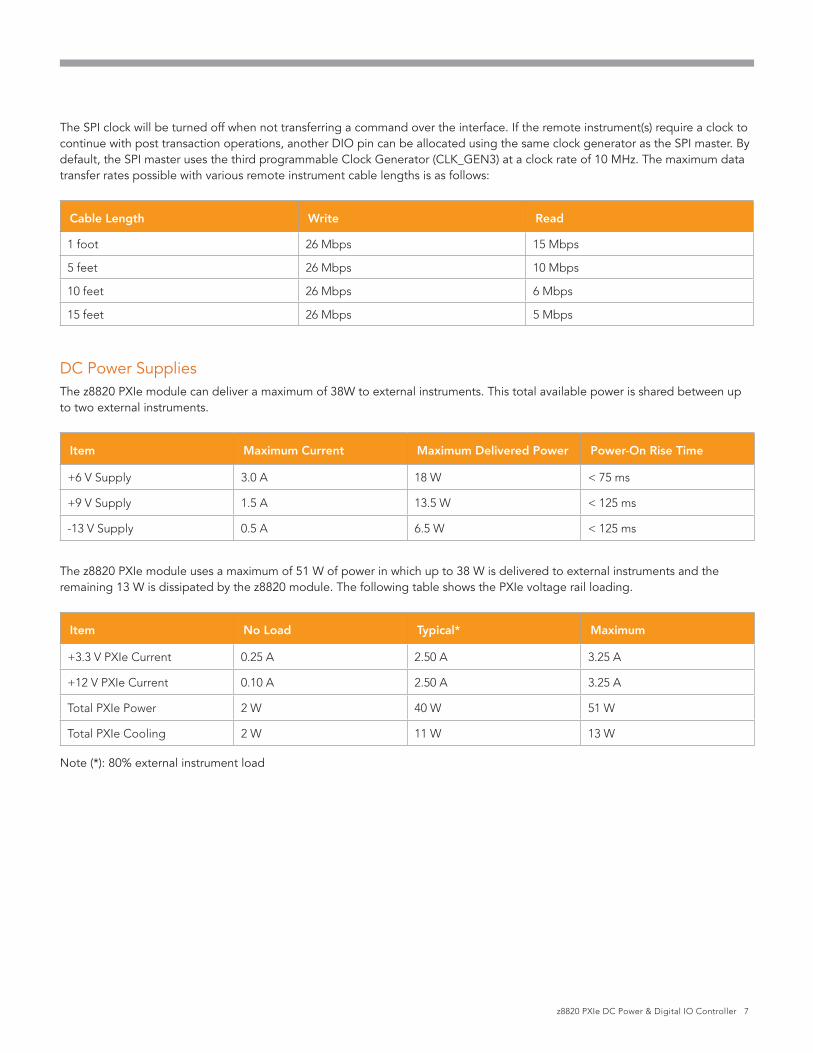
The SPI clock will be turned off when not transferring a command over the interface. If the remote instrument(s) require a clock to continue with post transaction operations, another DIO pin can be allocated using the same clock generator as the SPI master. By default, the SPI master uses the third programmable Clock Generator (CLK_GEN3) at a clock rate of 10 MHz. The maximum data transfer rates possible with various remote instrument cable lengths is as follows:
Cable Length Write Read
1 foot 26 Mbps 15 Mbps
5 feet 26 Mbps 10 Mbps
10 feet 26 Mbps 6 Mbps
15 feet 26 Mbps 5 Mbps
DC Power SuppliesThe z8820 PXIe module can deliver a maximum of 38W to external instruments. This total available power is shared between up to two external instruments.
Item Maximum Current Maximum Delivered Power Power-On Rise Time
+6 V Supply 3.0 A 18 W < 75 ms
+9 V Supply 1.5 A 13.5 W < 125 ms
-13 V Supply 0.5 A 6.5 W < 125 ms
The z8820 PXIe module uses a maximum of 51 W of power in which up to 38 W is delivered to external instruments and the remaining 13 W is dissipated by the z8820 module. The following table shows the PXIe voltage rail loading.
Item No Load Typical* Maximum
+3.3 V PXIe Current 0.25 A 2.50 A 3.25 A
+12 V PXIe Current 0.10 A 2.50 A 3.25 A
Total PXIe Power 2 W 40 W 51 W
Total PXIe Cooling 2 W 11 W 13 W
Note (*): 80% external instrument load
z8820 PXIe DC Power & Digital IO Controller 8
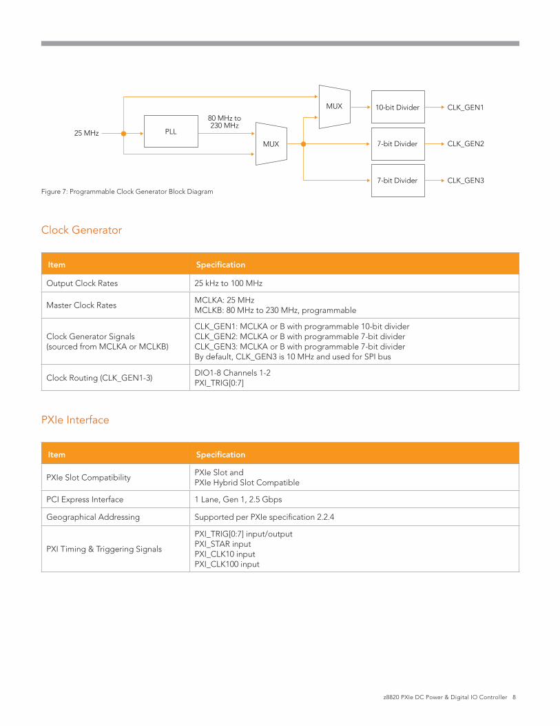
Clock Generator
Item Specification
Output Clock Rates 25 kHz to 100 MHz
Master Clock RatesMCLKA: 25 MHz MCLKB: 80 MHz to 230 MHz, programmable
Clock Generator Signals(sourced from MCLKA or MCLKB)
CLK_GEN1: MCLKA or B with programmable 10-bit dividerCLK_GEN2: MCLKA or B with programmable 7-bit dividerCLK_GEN3: MCLKA or B with programmable 7-bit dividerBy default, CLK_GEN3 is 10 MHz and used for SPI bus
Clock Routing (CLK_GEN1-3)DIO1-8 Channels 1-2PXI_TRIG[0:7]
PXIe Interface
Item Specification
PXIe Slot CompatibilityPXIe Slot and PXIe Hybrid Slot Compatible
PCI Express Interface 1 Lane, Gen 1, 2.5 Gbps
Geographical Addressing Supported per PXIe specification 2.2.4
PXI Timing & Triggering Signals
PXI_TRIG[0:7] input/outputPXI_STAR inputPXI_CLK10 inputPXI_CLK100 input
MUX
MUX
PLL
80 MHz to230 MHz
25 MHz
10-bit Divider
7-bit Divider
7-bit Divider
CLK_GEN1
CLK_GEN2
CLK_GEN3
Figure 7: Programmable Clock Generator Block Diagram

z8820 PXIe DC Power & Digital IO Controller 9
Physical & Environmental Size & Weight
Item Specification
Physical SizeSingle-Wide 3U PXIe Instrument8.25” x 0.79” x 5.25” (L x W x H)20.96 cm x 2.01 cm x 13.34 cm (L x W x H)
Weight 6.3 oz. (178 g)
Temperature Range
Item Specification
Operating 0°C to +40°C ambient (MIL-PRF28800F Class 3)
Storage -40°C to +75°C (MIL-PRF28800F Class 3)
Relative Humidity
Item Specification
Operating or Storage Up to +30°C +30°C to +40°C above +40 °C
5 to 95% ± 5% non-condensing5 to 75% ± 5% non-condensing5 to 45% ± 5% non-condensing

z8820 PXIe DC Power & Digital IO Controller 10
Terminology
Numeric PrefixesWhen referring to numeric values, this document will use SI (International System of Units) and IEC (International Electrotechnical Commission) standard prefixes. Prefix definitions are in the following table.
Prefix Multiplier
n (nano) 1/(1000x1000x1000)
µ (micro) 1/(1000x1000)
m (milli) 1/1000
k/K (kilo) 1000
M (Mega) 1000x1000
G (Giga) 1000x1000x1000
Ki (Kibi) 1024
Mi (Mebi) 1024x1024
Gi (Gibi) 1024x1024x1024
Differential OutputsSingle-Ended is used to refer to the output on either the + or – output pin
Differential is used to refer to the output between the + and- output pins
Vd indicates Volts differential
Vppd indicates Volts peak-to-peak differential
z8820 PXIe DC Power & Digital IO Controller 11
SafetyThis product is designed to meet the requirements of the following standard of safety for electrical equipment for measurement, control and laboratory use: EN 61010-1
Electromagnetic CompatibilityCE Marking EN 61326-1:1997 with A1:1998 and A2:2001 Compliant
FCC Part 15 (Class A) Compliant
EmissionsEN 55011 Radiated Emissions, ISM Group 1, Class A, distance 10 m, emissions < 1 GHzEN 55011 Conducted Emissions, Class A, emissions < 30 MHz ImmunityEN 61000-4-2 Electrostatic Discharge (ESD), 4 kV by Contact, 8 kV by AirEN 61000-4-3 RF Radiated Susceptibility, 10 V/mEN 61000-4-4 Electrical Fast Transient Burst (EFTB), 2 kV AC Power LinesEN 61000-4-5 SurgeEN 61000-4-6 Conducted ImmunityEN 61000-4-8 Power Frequency Magnetic Field, 30 A/mEN 61000-4-11 Voltage Dips and Interrupts
CE ComplianceThis product meets the necessary requirements of applicable European Directives for CE Marking as follows:
73/23/EEC Low Voltage Directive (Safety)89/336/EEC Electromagnetic Compatibility Directive (EMC)
See Declaration of Conformity for this product for additional regulatory compliance information.

Copyright © 2016 LitePoint, A Teradyne Company.
All rights reserved
RESTRICTED RIGHTS LEGENDNo part of this document may bereproduced, transmitted, transcribed,stored in a retrieval system, or translated into any language or computer language, in any form or by any means, electronic, mechanical, magnetic, optical, chemical, manual, or otherwise, without the prior written permission of LitePoint Corporation.
DISCLAIMERLitePoint Corporation makes norepresentations or warranties withrespect to the contents of this manual or of the associated LitePoint Corporation products, and specifically disclaims any implied warranties of merchantability or fitness for any particular purpose. LitePoint Corporation shall under nocircumstances be liable for incidentalor consequential damages or relatedexpenses resulting from the use of thisproduct, even if it has been notified ofthe possibility of such damages.
If you find errors or problems with thisdocumentation, please notify LitePointCorporation at the address listedbelow. LitePoint Corporation does notguarantee that this document is error-free. LitePoint Corporation reserves theright to make changes in specificationsand other information contained in thisdocument without prior notice.
CONTACT INFORMATIONLitePoint Corporation965 W. Maude Ave.Sunnyvale, CA 94085-2803United States of America Telephone: +1.408.456.5000
LITEPOINT TECHNICAL SUPPORTwww.litepoint.com/support
Doc: 1075-1003-001 November 2016 Rev 1
TRADEMARKSLitePoint and the LitePoint logo are registered trademarks of LitePoint Corporation. z8820 is a trademark of LitePoint Corporation. All other trademarks or registered trademarks are owned by their respective owners.