xilinx isim - new paltzbai/egc208/isim simulator_verilog_14.1.pdf · xilinx isim simulation...
TRANSCRIPT

Department of Electrical and Computer Engineering
Xilinx ISIM <Release Version: 14.1i>
Simulation Tutorial
Using Verilog
© Spring 2013
Baback Izadi
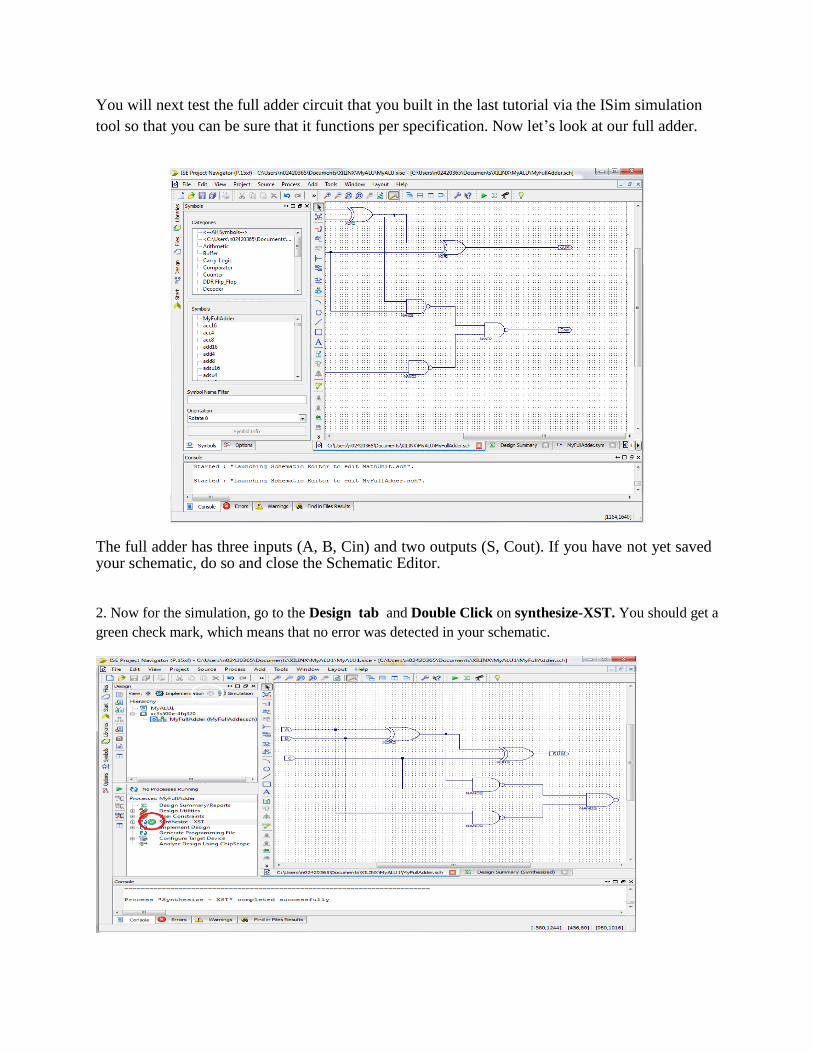
You will next test the full adder circuit that you built in the last tutorial via the ISim simulation
tool so that you can be sure that it functions per specification. Now let’s look at our full adder.
The full adder has three inputs (A, B, Cin) and two outputs (S, Cout). If you have not yet saved your schematic, do so and close the Schematic Editor.
2. Now for the simulation, go to the Design tab and Double Click on synthesize-XST. You should get a
green check mark, which means that no error was detected in your schematic.
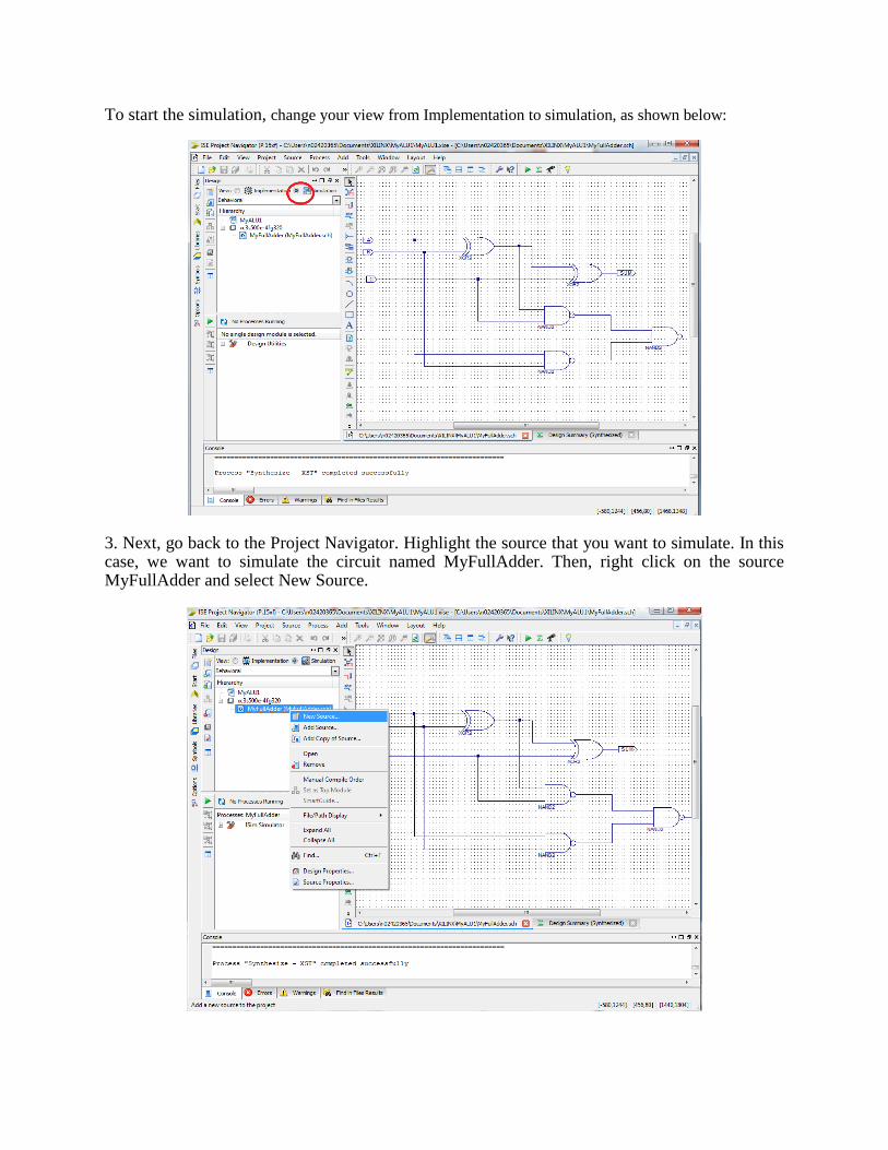
To start the simulation, change your view from Implementation to simulation, as shown below:
3. Next, go back to the Project Navigator. Highlight the source that you want to simulate. In this case, we want to simulate the circuit named MyFullAdder. Then, right click on the source MyFullAdder and select New Source.
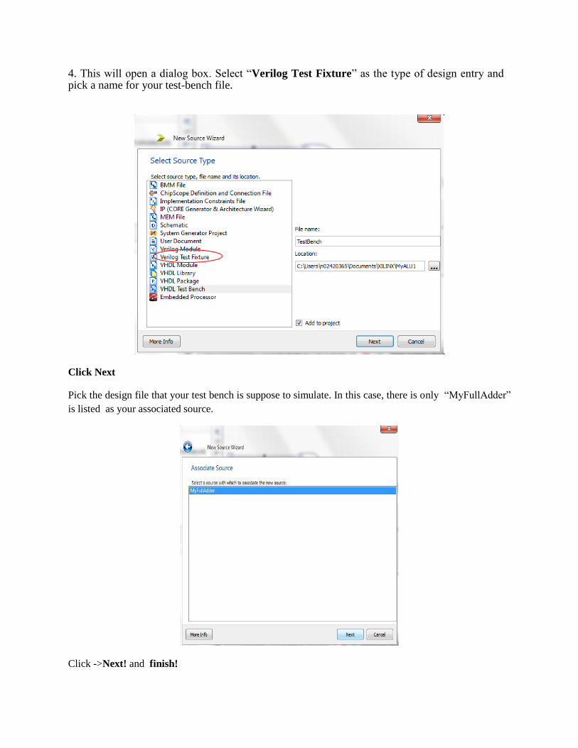
4. This will open a dialog box. Select “Verilog Test Fixture” as the type of design entry and pick a name for your test-bench file.
Click Next
Pick the design file that your test bench is suppose to simulate. In this case, there is only “MyFullAdder”
is listed as your associated source.
Click ->Next! and finish!
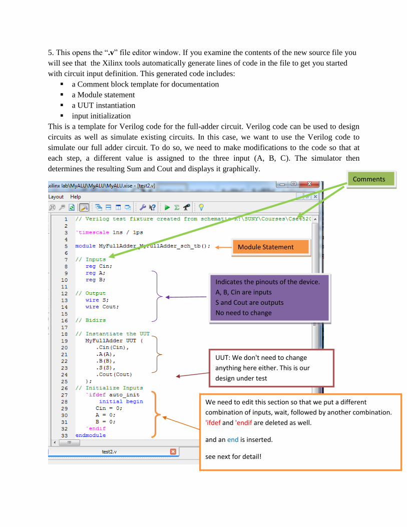
5. This opens the “.v” file editor window. If you examine the contents of the new source file you
will see that the Xilinx tools automatically generate lines of code in the file to get you started
with circuit input definition. This generated code includes:
a Comment block template for documentation
a Module statement
a UUT instantiation
input initialization
This is a template for Verilog code for the full-adder circuit. Verilog code can be used to design
circuits as well as simulate existing circuits. In this case, we want to use the Verilog code to
simulate our full adder circuit. To do so, we need to make modifications to the code so that at
each step, a different value is assigned to the three input (A, B, C). The simulator then
determines the resulting Sum and Cout and displays it graphically.
Comments
Indicates the pinouts of the device.
A, B, Cin are inputs
S and Cout are outputs
No need to change
UUT: We don't need to change
anything here either. This is our
design under test
We need to edit this section so that we put a different
combination of inputs, wait, followed by another combination.
'ifdef and 'endif are deleted as well.
and an end is inserted.
see next for detail!
Module Statement
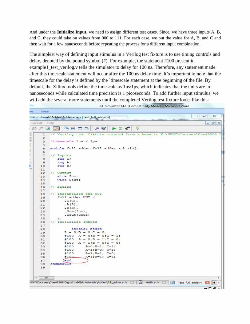
And under the Initialize Input, we need to assign different test cases. Since, we have three inputs A, B,
and C, they could take on values from 000 to 111. For each case, we put the value for A, B, and C and
then wait for a few nanoseconds before repeating the process for a different input combination.
The simplest way of defining input stimulus in a Verilog test fixture is to use timing controls and
delay, denoted by the pound symbol (#). For example, the statement #100 present in
example1_test_verilog.v tells the simulator to delay for 100 ns. Therefore, any statement made
after this timescale statement will occur after the 100 ns delay time. It’s important to note that the
timescale for the delay is defined by the `timescale statement at the beginning of the file. By
default, the Xilinx tools define the timescale as 1ns/1ps, which indicates that the units are in
nanoseconds while calculated time precision is 1 picoseconds. To add further input stimulus, we
will add the several more statements until the completed Verilog test fixture looks like this:

6. Next, highlight the “.v” file on the left hand side of the window under the design section, and expand
the ISim Simulator.
8. Double click on the Behavioral Check Syntax
7. Once you see the green check mark double click on the Simulate Behavioral Model.

8. This will open the waveform “ISIM window”. ZOOM to the full view. Now you can see the
waveforms of your full adder that you just simulated.
You can position the cursor on the various points and see the corresponding value displayed on the left
side of the display. For example, for the current cursor position, C=1, A = 1, B = 1 resulting in Sum = 1
and Cout = 1; which is the correct result.
Once you are convinced that your design is correct, you can move the next step in your design entry.

If you have different cases of stimulus that you wish to try out in the simulator, simply close
ISim, edit the Verilog test fixture in ISE’s text editor, and rerun the Simulate Behavioral Model
process to open ISim again.
GOOD LUCK!!