x8da3 i qrg 1.00 (mnl-1031-qrg) - super micro …€¦ · · 2015-06-03mnl-1031-q r g r e v. 1.00...
TRANSCRIPT
SUPERMICR R CONTACT INFORMATION • www.supermicro.com (Email: [email protected])• Manuals: http://www.supermicro.com/support/manuals• Drivers & Utilities: ftp://ftp.supermicro.com• Safety: http://www.supermicro.com/about/policies/safety_information.cfm
PACKAGE CONTENTS (Applies to single-pack only)
X8DA3 / X8DAiQUICK REFEREN CE GUIDE
• One (1) Supermicro Motherboard• One (1) Floppy Ribbon Cable• One (1) 1394a Connector Cable• Two (2) SAS Cables (for X8DA3)
• Four (4) Serial ATA Cables (for X8DA3)• Six (6) Serial ATA Cables (for X8DAi)• One (1) I/O Back Panel Shield
MN
L-10
31-Q
RG R
EV
. 1.0
0©
201
2 S
uper
mic
ro C
ompu
ter
Inc.
A
ll rig
hts
rese
rved
. R
epro
duct
ion
of t
his
docu
men
t w
heth
er in
par
t or
in w
hole
is s
tric
tly p
rohi
bite
d w
ithou
t S
uper
mic
ro's
writ
ten
cons
ent.
All
Trad
emar
ks a
re p
rope
rty
of t
heir
resp
ectiv
e en
titie
s. A
ll in
form
atio
n pr
ovid
ed is
dee
med
acc
urat
e at
the
tim
e of
prin
ting;
how
ever
, it
is n
ot g
uara
ntee
d.
JWOL1
JC2
JSM1 JSM2
J5
JPS1
JPI1
JI2C2
JI2C1
JPL2
1JI2C
3JI2C
4JPL1
JF1
LE1
LES1LES2
JPI2C
JD1
SP1
JL1
JPS2
KB/Mouse
JPW
3JP
W1
JPW
2
Fan8/CPU
1 Fan
Fan6Fan5
Fan2
Fan4 Fan3
Fan7/CP
U2
Fan1
Slot5 P
CI 33M
H
Slot4 P
CI 33M
H
Slot3 P
CI-E
X16
P2 D
IMM
3A
USB0/1/2/3
COM1AUDIO
JBT1
Slot2 P
CI-E
X4
I-SATA0I-SATA1
I-SATA4I-SATA5
JWD1
Slot1 P
CI 33M
H
T-SGPIO2
Slot0 S
IMLC
Floppy
USB6/7
USB4/5
US
B8
COM2
LANCTRL
LANCTRL
CD
1
Slot6 P
CI-E
x16
SPI BIOS
I-Button
I-SATA3I-SATA2
JOH1
X8D
A3/i
Battery
SAS 0~3 SAS 4~7
82573V82573L
SAS CTRL
1068E
LAN1/2
Intel 5520
Intel ICH10R South Bridge
P2 D
IMM
3BP
2 DIM
M2A
P2 D
IMM
2BP
2 DIM
M1A
P2 D
IMM
1B
P1 D
IMM
3AP
1 DIM
M3B
P1 D
IMM
2AP
1 DIM
M2B
P1 D
IMM
1AP
1 DIM
M1B
IOH-36D
S I/O
T-SGPIO1
1394CTRL
JFDD1
CNF1 CNF2
US
B9
JWF1
CPU1
CPU2
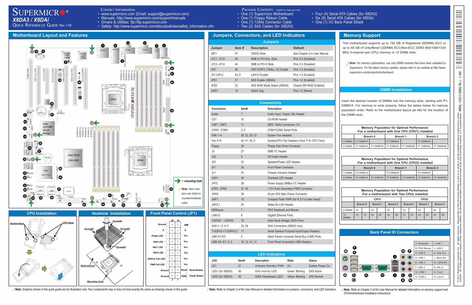
Motherboard Layout and Features
CPU Installation
DIMM Installation
Jumpers, Connectors, and LED Indicators
Connectors
Memory Support
Insert the desired number of DIMMs into the memory slots, starting with P1-DIMM1A. For memory to work properly, follow the tables below for memory population order. Refer to the motherboard layout (at left) for the location of the DIMM slots.
Memory Population for Optimal Performance-For a motherboard with One CPU (CPU1) installed
Branch 0 Branch 1 Branch 2
3 DIMMs P1 DIMM1A P1 DIMM2A P1 DIMM3A
6 DIMMs P1 DIMM1A P1 DIMM1B P1 DIMM2A P1 DIMM2B P1 DIMM3A P1 DIMM3B
Memory Population for Optimal Performance-For a motherboard with One CPU (CPU2) installed
Branch 0 Branch 1 Branch 2
3 DIMMs P2 DIMM1A P2 DIMM2A P2 DIMM3A
6 DIMMs P2 DIMM1A P2 DIMM1B P2 DIMM2A P2 DIMM2B P2 DIMM3A P2 DIMM3B
Memory Population for Optimal Performance-For a motherboard with Two CPUs installed
CPU1 CPU2
Branch 0 Branch 1 Branch 2 Branch 0 Branch 1 Branch 2
6 DIMMs 1A 2A 3A 1A 2A 3A
12 DIMMs
1A 1B 2A 2B 3A 3B 1A 1B 2A 2B 3A 3B
Note: Refer to Chapter 2 of the User Manual for detailed information on memory support and CPU/motherboard installation instructions.
Heatsink Installation Front Panel Control (JF1)
Note: Refer to Chapter 2 of the User Manual on detailed information on jumpers, connectors, and LED indicators.Note: Graphics shown in this quick guide are for illustration only. Your components may or may not look exactly the same as drawings shown in this guide.
Back Panel IO Connectors
LED Indicators
Connectors Item# DescriptionAudio 7 Audio Input, Output, Mic HeaderCD1 10 CD-ROM HeaderCNF1, CNF2 11 IEEE 1394a Connectors 1/2COM1, COM2 3, 4 COM1/COM2 Serial Ports FAN 1~4 36, 32, 29, 23 System Fan Headers Fan 5~8 42, 41, 35, 5 System/CPU Fan Headers (Fans 7~8: CPU Fans)Floppy 28 Floppy Disk Drive ConnectorJ5 27 SMB I2C HeaderJC2 9 HD Audio HeaderJD1 33 Speaker/Power LED HeaderJF1 30 Front Panel ConnectorJL1 20 Chassis Intrusion HeaderJOH1 34 Overheat LED HeaderJPI2C 38 Power Supply SMBus I2C HeaderJPW1, JPW2 37, 40 +12V 8-pin Secondary PWR Connector JPW3 39 24-pin ATX Main Power Connector JWF1 18 Compact Flash PWR (for R 2.0 or later board)JWOL1 24 Wake-On-LAN HeaderKB/Mouse 1 PS/2 Keyboard and MouseLAN1/2 6 Gigabit Ethernet PortsI-SATA0 ~ I-SATA5 15 (Intel South Bridge) SATA PortsSAS 0 ~3, 4~7 25, 26 SAS Connectors (X8DA3 only)T-SGPIO-1/T-SGPIO-2 17 Serial General Purpose Input/Output HeadersUSB 0/1/2/3 2 (Back Panel) Universal Serial Bus (USB) PortsUSB 4/5, 6/7, 8, 9 16, 12, 14, 13 Front Panel Accessible USB Headers
LED Item# Description State StatusLE1 31 Onboard Standby PWR On System Power OnLES1 (for X8DA3) 49 SAS Activity LED Green: Blinking SAS ActiveLES2 (for X8DA3) 48 SAS Heartbeat LED Yellow: Blinking SAS Normal
Jumpers This motherboard supports up to 192 GB of Registered (RDIMM) ECC or up to 48 GB of Unbuffered (UDIMM) ECC/Non-ECC DDR3 800/1066/1333 MHz 3-channel (per CPU) memory in 12 DIMM slots.
Note: For memory optimization, use only DIMM modules that have been validated by Supermicro. For the latest memory updates, please refer to our website at http://www.supermicro.com/products/motherboard.
A
B
CD
E
F
G H I
J
KL
M
O
P
Note: Item num-bers are listed in counterclockwise order.
= mounting hole
A. Keyboard I. LAN 1
B. PS/2 Mouse J. LAN 2
C. USB 0 K. Side Sur
D. USB 1 L. Back Sur
E. USB 2 M. CEN/LFE
F. USB 3 N. Mic In
G. COM 1 O. Front
H. COM 2 P. Line-In
Motherboard
Screw#1 Screw#2
Mounting Hole
Screw#3
Screw#4
Jumper Item # Description Default
JBT1 47 CMOS Clear See Chapter 2 in User ManualJI2C1, JI2C2 45 SMB to PCI-Exp. Slots Pins 2-3 (Disabled)JI2C3, JI2C4 44 SMB to PCI-X Slots Pins 2-3 (Disabled)JPI1 46 CNF1/CNF2 (1394a_1/2) Enable Pins 1-2 (Enabled)JPL1/JPL2 43, 8 LAN1/2 Enable Pins 1-2 (Enabled)JPS1 21 SAS Enable (X8DA3) Pins 1-2 (Enabled)JPS2 22 SAS RAID Mode Select (X8DA3) Closed (SR RAID Enabled)JWD1 19 Watch Dog Pins 1-2 (Reset)
Socket Keys CPU Keys
Power Button
OH/Fan Fail LED
1
NIC1 LED
Reset Button
2
HDD LED
Power LED
Reset
PWR
Vcc
Vcc
Vcc
Vcc
Ground
Ground
1920
Vcc
X
Ground NMI
X
Vcc
PWR Fail LED
NIC2 LED
N
15
19
114
110
115
14
18
113
1317
112
117
118
119
120
1216
111
116
121
126131
136
141
137
142
143
144
145
138
139
140
132 133
134
135
127
128 129 130
122
123124 125
11
146
147
148
149
Rev. 1.00