wl1837modcom8i wlan mimo and bluetooth module …
TRANSCRIPT
User’s GuideWL1837MODCOM8I WLAN MIMO and Bluetooth® Module Evaluation Board for TI Sitara™ Platform
ABSTRACT
The WL1837MODCOM8I is a Wi-Fi® dual-band, Bluetooth®, and BLE module evaluation board (EVB) with the TI WL1837 module (WL1837MOD, with Bluetooth) or WL1807 module (WL1807MOD, without Bluetooth). The WL18x7MOD is a certified WiLink™ 8 module from TI that offers high throughput and extended range along with Wi-Fi and Bluetooth coexistence in a power-optimized design. The WL1807MOD offers A 2.4- and 5-GHz module solution with two antennas supporting industrial temperature grade. The module is FCC, IC, ETSI/CE, and TELEC certified for AP (with DFS support) and client. TI offers drivers for high-level operating systems, such as Linux®, Android™, WinCE, and RTOS.TI.
Table of Contents1 Trademarks..............................................................................................................................................................................2Warning.......................................................................................................................................................................................22 Overview..................................................................................................................................................................................3
2.1 General Features............................................................................................................................................................... 32.2 Key Benefits....................................................................................................................................................................... 32.3 Applications........................................................................................................................................................................4
3 Board Pin Assignment........................................................................................................................................................... 43.1 Pin Description................................................................................................................................................................... 53.2 Jumper Connections.......................................................................................................................................................... 7
4 Electrical Characteristics.......................................................................................................................................................75 Approved Antenna Types and Maximum Gain Values........................................................................................................ 76 Antenna Characteristics........................................................................................................................................................ 8
6.1 VSWR.................................................................................................................................................................................86.2 Efficiency............................................................................................................................................................................96.3 Radio Pattern..................................................................................................................................................................... 9
7 Circuit Design........................................................................................................................................................................107.1 EVB Reference Schematics.............................................................................................................................................107.2 Bill of Materials (BOM)......................................................................................................................................................11
8 Layout Guidelines.................................................................................................................................................................128.1 Board Layout....................................................................................................................................................................12
9 Ordering Information............................................................................................................................................................1810 Revision History................................................................................................................................................................. 18
List of FiguresFigure 2-1. WL1837MODCOM8I EVB (Top View)....................................................................................................................... 3Figure 3-1. EVB Top View............................................................................................................................................................4Figure 3-2. EVB (Bottom View)....................................................................................................................................................4Figure 6-1. Antenna VSWR Characteristics................................................................................................................................ 8Figure 6-2. Antenna Efficiency.....................................................................................................................................................9Figure 7-1. EVB Reference Schematics.................................................................................................................................... 10Figure 8-1. WL1837MODCOM8I Layer 1 Layout...................................................................................................................... 12Figure 8-2. WL1837MODCOM8I Layer 2 Layout...................................................................................................................... 12Figure 8-3. WL1837MODCOM8I Layer 3 Layout...................................................................................................................... 13Figure 8-4. WL1837MODCOM8I Layer 4 Layout...................................................................................................................... 13Figure 8-5. Module Layout Guidelines (Top Layer)....................................................................................................................14Figure 8-6. Module Layout Guidelines (Bottom Layer).............................................................................................................. 14Figure 8-7. Trace Design for the PCB Layout............................................................................................................................15
www.ti.com Table of Contents
SWRU382C – JANUARY 2015 – REVISED DECEMBER 2021Submit Document Feedback
WL1837MODCOM8I WLAN MIMO and Bluetooth® Module Evaluation Board for TI Sitara™ Platform
1
Copyright © 2021 Texas Instruments Incorporated

Figure 8-8. Layer 1 Combined With Layer 2..............................................................................................................................15Figure 8-9. Top Layer – Antenna and RF Trace Routing Layout Guidelines............................................................................. 16Figure 8-10. Bottom Layer – Antenna and RF Trace Routing Layout Guidelines......................................................................16Figure 8-11. MIMO Antenna Spacing.........................................................................................................................................17
List of TablesTable 3-1. Pin Description............................................................................................................................................................5Table 5-1. Approved Antenna Types and Maximum Gain Values................................................................................................7Table 7-1. BOM.......................................................................................................................................................................... 11Table 8-1. Module Layout Guidelines........................................................................................................................................ 14Table 8-2. Antenna and RF Trace Routing Layout Guidelines...................................................................................................17
1 TrademarksSitara™ and WiLink™ are trademarks of TI.Android™ is a trademark of Google, Inc.Bluetooth® are registered trademarks of Bluetooth SIG, Inc.Wi-Fi® is a registered trademark of Wi-Fi Alliance.Linux® is a registered trademark of Linus Torvalds.All trademarks are the property of their respective owners.
WarningThe WL1837MODCOM8I board is tested to comply with ETSI/R&TTE over temperatures from –40°C to +85°C.
This board should not be modified to operate in other frequency bands other than what they are designed for.
FCC Licensing Requirements for the Wi-Fi and Bluetooth Radio Module of the EVM:
For evaluation only; not FCC approved for resale. This kit is designed to allow:
1. Product developers to evaluate electronic components, circuitry, or software associated with the kit to determine whether to incorporate such items in a finished product
2. Software developers to write software applications for use with the end product. This kit is not a finished product and when assembled may not be resold or otherwise marketed unless all required FCC equipment authorizations are first obtained. Operation is subject to the condition that this product not cause harmful interference to licensed radio stations and that this product accept harmful interference. Unless the assembled kit is designed to operate under part 15, part 18, or part 95 of this chapter, the operator of the kit must operate under the authority of an FCC license holder or must secure an experimental authorization under part 5 of this chapter.
Per TI’s Regulatory Compliance Information located in the WL1837MODCOM8I User’s Guide’s “Evaluation Board/Kit/Module (EVM) Additional Terms,” this EVM cannot be used for production purposes and is explicitly restricted from end-product introduction.
Use of this EVM requires the developer to provide a minimum distance of at least 20 cm from the antenna to all persons in order to minimize risk of potential radiation hazards.
CAUTION
Do not leave the EVM powered when unattended.
Trademarks www.ti.com
2 WL1837MODCOM8I WLAN MIMO and Bluetooth® Module Evaluation Board for TI Sitara™ Platform
SWRU382C – JANUARY 2015 – REVISED DECEMBER 2021Submit Document Feedback
Copyright © 2021 Texas Instruments Incorporated
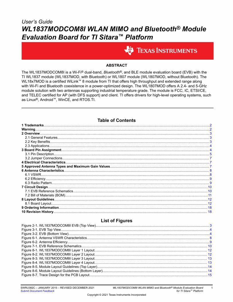
2 OverviewFigure 2-1 shows the WL1837MODCOM8I EVB.
U1
WL1837MODGI
Figure 2-1. WL1837MODCOM8I EVB (Top View)
2.1 General FeaturesThe WL1837MODCOM8I EVB includes the following features:
• WLAN, Bluetooth, and BLE on a single module board• 100-pin board card• Dimensions: 76.0 mm (L) x 31.0 mm (W)• WLAN 2.4- and 5-GHz SISO (20- and 40-MHz channels), 2.4-GHz MIMO (20-MHz channels)• Support for BLE dual mode• Seamless integration with TI Sitara and other application processors• Design for the TI AM335X general-purpose evaluation module (EVM)• WLAN and Bluetooth, BLE, and ANT cores that are software- and hardware-compatible with prior WL127x,
WL128x, and BL6450 offerings for smooth migration to device• Shared host-controller-interface (HCI) transport for Bluetooth, BLE, and ANT using UART and SDIO for
WLAN• Wi-Fi and Bluetooth single-antenna coexistence• Built-in chip antenna• Optional U.FL RF connector for external antenna• Direct connection to the battery using an external switched-mode power supply (SMPS) supporting 2.9- to
4.8-V operation• VIO in the 1.8-V domain
2.2 Key BenefitsThe WL18x7MOD offers the following benefits:
• Reduces design overhead: Single WiLink 8 module scales across Wi-Fi and Bluetooth• WLAN high throughput: 80 Mbps (TCP), 100 Mbps (UDP)• Bluetooth 4.2 (5.1 compliant) + BLE (Smart Ready)• Wi-Fi and Bluetooth single-antenna coexistence• Low power at 30% to 50% less than the previous generation• Available as an easy-to-use FCC-, ETSI-, and Telec-certified module• Lower manufacturing costs saves board space and minimizes RF expertise.• AM335x Linux and Android reference platform accelerates customer development and time to market.
www.ti.com Overview
SWRU382C – JANUARY 2015 – REVISED DECEMBER 2021Submit Document Feedback
WL1837MODCOM8I WLAN MIMO and Bluetooth® Module Evaluation Board for TI Sitara™ Platform
3
Copyright © 2021 Texas Instruments Incorporated
2.3 ApplicationsThe WL1837MODCOM8I device is designed for the following applications:
• Portable consumer devices• Home electronics• Home appliances and white goods• Industrial and home automation• Smart gateway and metering• Video conferencing• Video camera and security
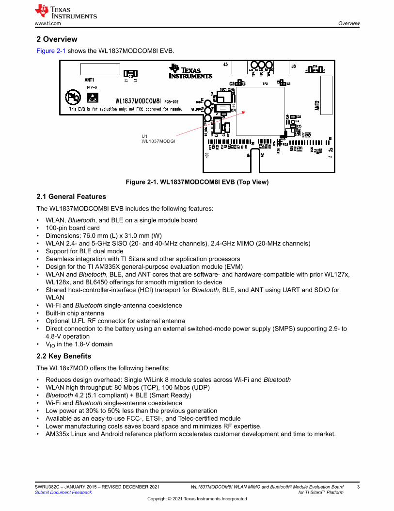
3 Board Pin AssignmentFigure 3-1 shows the top view of the EVB.
Figure 3-1. EVB Top View
Figure 3-2 shows the bottom view of the EVB.
Figure 3-2. EVB (Bottom View)
Overview www.ti.com
4 WL1837MODCOM8I WLAN MIMO and Bluetooth® Module Evaluation Board for TI Sitara™ Platform
SWRU382C – JANUARY 2015 – REVISED DECEMBER 2021Submit Document Feedback
Copyright © 2021 Texas Instruments Incorporated

3.1 Pin DescriptionTable 3-1 describes the board pins.
Table 3-1. Pin DescriptionNo. Name Type Description1 SLOW_CLK I Slow clock input option (default: NU)
2 GND G Ground
3 GND G Ground
4 WL_EN I WLAN enable
5 VBAT P 3.6-V typical voltage input
6 GND G Ground
7 VBAT P 3.6-V typical voltage input
8 VIO P VIO 1.8-V (I/O voltage) input
9 GND G Ground
10 N.C. No connection
11 WL_RS232_TX O WLAN tool RS232 output
12 N.C. No connection
13 WL_RS232_RX I WLAN tool RS232 input
14 N.C. No connection
15 WL_UART_DBG O WLAN Logger output
16 N.C. No connection
17 N.C. No connection
18 GND G Ground
19 GND G Ground
20 SDIO_CLK I WLAN SDIO clock
21 N.C. No connection
22 GND G Ground
23 N.C. No connection
24 SDIO_CMD I/O WLAN SDIO command
25 N.C. No connection
26 SDIO_D0 I/O WLAN SDIO data bit 0
27 N.C. No connection
28 SDIO_D1 I/O WLAN SDIO data bit 1
29 N.C. No connection
30 SDIO_D2 I/O WLAN SDIO data bit 2
31 N.C. No connection
32 SDIO_D3 I/O WLAN SDIO data bit 3
33 N.C. No connection
34 WLAN_IRQ O WLAN SDIO interrupt out
35 N.C. No connection
36 N.C. No connection
37 GND G Ground
38 N.C. No connection
39 N.C. No connection
40 N.C. No connection
41 N.C. No connection
42 GND G Ground
43 N.C. No connection
44 N.C. No connection
www.ti.com Board Pin Assignment
SWRU382C – JANUARY 2015 – REVISED DECEMBER 2021Submit Document Feedback
WL1837MODCOM8I WLAN MIMO and Bluetooth® Module Evaluation Board for TI Sitara™ Platform
5
Copyright © 2021 Texas Instruments Incorporated

Table 3-1. Pin Description (continued)No. Name Type Description45 N.C. No connection
46 N.C. No connection
47 GND G Ground
48 N.C. No connection
49 N.C. No connection
50 N.C. No connection
51 N.C. No connection
52 PCM_IF_CLK I/O Bluetooth PCM clock input or output
53 N.C. No connection
54 PCM_IF_FSYNC I/O Bluetooth PCM frame sync input or output
55 N.C. No connection
56 PCM_IF_DIN I Bluetooth PCM data input
57 N.C. No connection
58 PCM_IF_DOUT O Bluetooth PCM data output
59 N.C. No connection
60 GND G Ground
61 N.C. No connection
62 N.C. No connection
63 GND G Ground
64 GND G Ground
65 N.C. No connection
66 BT_UART_IF_TX O Bluetooth HCI UART transmit output
67 N.C. No connection
68 BT_UART_IF_RX I Bluetooth HCI UART receive input
69 N.C. No connection
70 BT_UART_IF_CTS I Bluetooth HCI UART Clear-to-Send input
71 N.C. No connection
72 BT_UART_IF_RTS O Bluetooth HCI UART Request-to-Send output
73 N.C. No connection
74 RESERVED1 O Reserved
75 N.C. No connection
76 BT_UART_DEBUG O Bluetooth Logger UART output
77 GND G Ground
78 GPIO9 I/O General-purpose I/O
79 N.C. No connection
80 N.C. No connection
81 N.C. No connection
82 N.C. No connection
83 GND G Ground
84 N.C. No connection
85 N.C. No connection
86 N.C. No connection
87 GND G Ground
88 N.C. No connection
89 BT_EN I Bluetooth enable
90 N.C. No connection
91 N.C. No connection
Board Pin Assignment www.ti.com
6 WL1837MODCOM8I WLAN MIMO and Bluetooth® Module Evaluation Board for TI Sitara™ Platform
SWRU382C – JANUARY 2015 – REVISED DECEMBER 2021Submit Document Feedback
Copyright © 2021 Texas Instruments Incorporated

Table 3-1. Pin Description (continued)No. Name Type Description92 GND G Ground
93 RESERVED2 I Reserved
94 N.C. No connection
95 GND G Ground
96 GPIO11 I/O General-purpose I/O
97 GND G Ground
98 GPIO12 I/O General-purpose I/O
99 TCXO_CLK_COM I Option to supply 26 MHz externally
100 GPIO10 I/O General-purpose I/O
3.2 Jumper ConnectionsThe WL1837MODCOM8I EVB includes the following jumper connections:
• J1: Jumper connector for VIO power input• J3: Jumper connector for VBAT power input• J5: RF connector for 2.4- and 5-GHz WLAN and Bluetooth• J6: Second RF connector for 2.4-GHz WLAN
4 Electrical CharacteristicsFor electrical characteristics, see the (WL18xxMOD WiLink™ Single-Band Combo Module – Wi-Fi®, Bluetooth®, and Bluetooth Low Energy (BLE) Data Sheet).
5 Approved Antenna Types and Maximum Gain ValuesThis device is intended only for OEM integrators under the following conditions:
• The antenna must be installed so that 20 cm is maintained between the antenna and users.• The transmitter module cannot be co-located with any other transmitter or antenna.• The radio transmitter can operate only using an antenna of a type and maximum (or lesser) gain approved
by TI. Table 5-1 lists the antennas approved by TI for use with the radio transmitter along with maximum allowable gain values. Antenna types not included in the list or having a gain greater than the maximum indicated are strictly prohibited for use with this transmitter.
Table 5-1. Approved Antenna Types and Maximum Gain ValuesAntenna Type Brand 2.4 GHz 4.9 to 5.9 GHz(1) Unit
PCB Ethertronics –0.600 4.50
dBi
Dipole LSR 2.00 2.00
PCB Laird 2.00 4.00
Chip Pulse 3.20 4.20
PIFA LSR 2.00 3.00
Chip TDK 2.27 3.96
(1) Range is approximate.
NoteIf these conditions cannot be met (for example, with certain laptop configurations or co-location with another transmitter), the FCC/IC authorization will not be considered valid and the FCC ID/IC ID cannot be used on the final product. In these circumstances, the OEM integrator is responsible for reevaluating the end product (including the transmitter) and obtaining a separate FCC/IC authorization.
www.ti.com Board Pin Assignment
SWRU382C – JANUARY 2015 – REVISED DECEMBER 2021Submit Document Feedback
WL1837MODCOM8I WLAN MIMO and Bluetooth® Module Evaluation Board for TI Sitara™ Platform
7
Copyright © 2021 Texas Instruments Incorporated
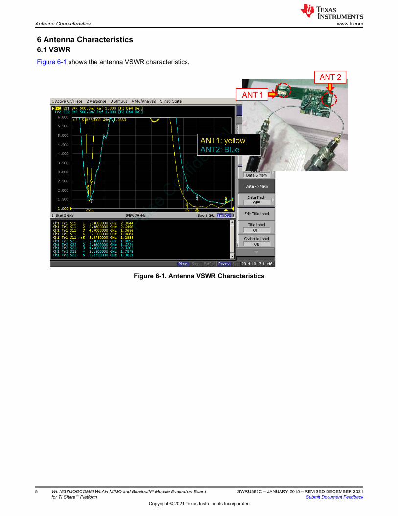
6 Antenna Characteristics6.1 VSWRFigure 6-1 shows the antenna VSWR characteristics.
Figure 6-1. Antenna VSWR Characteristics
Antenna Characteristics www.ti.com
8 WL1837MODCOM8I WLAN MIMO and Bluetooth® Module Evaluation Board for TI Sitara™ Platform
SWRU382C – JANUARY 2015 – REVISED DECEMBER 2021Submit Document Feedback
Copyright © 2021 Texas Instruments Incorporated

6.2 EfficiencyFigure 6-2 shows the antenna efficiency.
Figure 6-2. Antenna Efficiency
6.3 Radio PatternFor information on the antenna radio pattern and other related information, see productfinder.pulseeng.com/product/W3006.
www.ti.com Antenna Characteristics
SWRU382C – JANUARY 2015 – REVISED DECEMBER 2021Submit Document Feedback
WL1837MODCOM8I WLAN MIMO and Bluetooth® Module Evaluation Board for TI Sitara™ Platform
9
Copyright © 2021 Texas Instruments Incorporated

7 Circuit Design7.1 EVB Reference SchematicsFigure 7-1 shows the reference schematics for the EVB.
EDGE CONNECTOR - MALEANT2 - WL_2.4_IO1/WL_5GHzANT1 - WL_2.4_IO2/BT/WL_5GHz
R20 for test mode.
These two TPs for test modewhen WL_IRQ pull high.
WL_UART_DBG
BT_AUD_CLK
BT_AUD_FSYNC
BT_AUD_IN
WL_RS232_TX
WL_RS232_RX
BT_HCI_TX
BT_HCI_RX
BT_HCI_CTS
BT_HCI_RTS
BT_EN_SOC
BT_UART_DBG
SDIO_CLK_WL
SDIO_CMD_WL
SDIO_D0_WL
SDIO_D2_WL
SDIO_D3_WL
SDIO_D1_WL
WLAN_EN_SOC
BT_AUD_OUT
RESERVED1
GPIO9
GPIO11
GPIO12
GPIO10
SLOW_CLK
RESERVED2
WLAN_IRQ
RF_ANT1 RF_ANT2
SDIO_D3_WL
GPIO12
SDIO_D2_WL
GPIO11
SDIO_D0_WL
SDIO_D1_WL
GPIO9
WLAN_IRQ
GPIO10
RF_ANT2
WL_RS232_TX
WL_RS232_RX
RF_ANT1
RESERVED1
RESERVED2
BT_HCI_RX
BT_HCI_TX
BT_HCI_CTS
BT_HCI_RTS
BT_AUD_IN
BT_AUD_OUT
BT_AUD_CLK
BT_AUD_FSYNC
SDIO_CMD_WL
SDIO_CLK_WL
SLOW_CLK
WL_UART_DBG
BT_UART_DBG
BT_EN_SOC
WLAN_EN_SOC
EXT_CLK_REQ_OUT
EXT_CLK_REQ_OUT
TCXO_CLK_COM
TCXO_CLK_COM
VBAT_IN
VIO_IN
VIO_IN
VBAT_IN
VIO_IN
VIO_IN
VBAT_IN VIO_CLK
VIO_CLK
TP2 1
R14 0R 0402
R320R0603
L31.8nH0402
TP51
C210uF0603
J3NU_HEADER 1x2H-1X2_2MM
12
L11.3nH0402
R9 0R 0402
C142.4pF0402
R15 0R 0402
R8 0R 0402
R29 0R 0402
R12 0R 0402
R5 NU0402
R60R0402
J2NU_100pin Micro Edge MEC6SD-100P
1 2
3 4
5 6
7 8
9 10
11 12
13 14
15 16
17 18
19 20
21 22
23 24
25 26
27 28
29 30
31 32
33 34
35 36
37 38
39 40
41 42
43 44
45 46
47 48
49 50
51 52
53 54
55 56
57 58
59 60
61 62
63 64
65 66
67 68
69 70
71 72
73 74
75 76
77 78
79 80
81 82
83 84
85 86
87 88
89 90
91 92
93 94
95 96
97 98
99 100
0RR26 0402
R1 0R 0402
R13 0R 0402
R35NU0402
TCXO1NU_TCXO 26MHz2.0x1.6x0.73mm
NC1
VCC4
OUT3
GND2
TP81
C7NU_0R0402
R18 0R 0402
R7 0R 0402
TP41
TP1 1
C11uF0402
0RR24 0402
R310R0603
J6U.FL-R-SMT(10)U.FL
12
3
C50R0402
R28 0R 0402
TP31
R10 0R0402
R20 10k0402
TP6 1
R36 NU0402
L42.2nH0402
R34NU0402
U4NU_TLV70518XBGA-N4_0.8X0.8_0.4
VINB2
VOUTB1
ENA2
GNDA1
U1
WL1837MODGI
E-13.4X13.3-N100_0.75-TOP
GND17
VIO
38
VB
AT
47
EX
T_
32
K3
6
BT_AUD_FSYNC58
BT_AUD_IN56
BT_AUD_OUT57
BT_AUD_CLK60
WL_S
DIO
_D
212
WL_S
DIO
_C
LK
8
WL_S
DIO
_D
313
WL_S
DIO
_D
010
WL_S
DIO
_D
111
WL_S
DIO
_C
MD
6
BT_HCI_RTS50
BT_HCI_RX53
BT_HCI_TX52
BT_HCI_CTS51
GN
D16
GPIO_425
GPIO_226
GPIO_127
BT
_E
N_S
OC
41
WLA
N_IR
Q14
WLA
N_E
N_S
OC
40
BT
_U
AR
T_D
BG
43
WL_U
AR
T_D
BG
42
GNDG13
GNDG14
GNDG15
GNDG16
GNDG9
GNDG10
GN
D48
GNDG11
GNDG12
VB
AT
46
GND28
GNDG1
GNDG2
GNDG3
GNDG4
GNDG5
GNDG6
GNDG7
GNDG8
RF_ANT132
RESERVED64
GN
D1
GND20
RESERVED121
RESERVED222
GN
D37
GND19
RESERVED362
GNDG17
GNDG18
GNDG19
GNDG20
GNDG21
GNDG22
GNDG23
GNDG24
GNDG25
GNDG26
GNDG27
GNDG28
GNDG29
GNDG30
GNDG31
GNDG32
GNDG33
GNDG34
GNDG35
GND23
GND59
GN
D34
GND29
GN
D7
RF_ANT218
GND49
GN
D9
GND31
GN
D35
GN
D15
GND55
GN
D45
GN
D44
GND30
GND24
GND63
GND61
GN
D39
GN
D33
GND54
GNDG36
GP
IO11
2
GP
IO9
3
GP
IO10
4
GP
IO12
5
OSC11V8 / 32.768kHzOSC-3.2X2.5
EN1
VCC4
OUT3
GND2
ANT2W3006ANT-10.0X3.2MM_A
FEED1
NC2
R27 0R 0402
C40.1uF0402
0RR19 0402
C60R0402
C131pF0402
R16 0R 0402
R25 0R 0402
L2NU0402
R330R0402
C15NU_1uF0402
C8NU_0R0402
J5U.FL-R-SMT(10)U.FL
12
3
R3 0R 0402
0RR22 0402
R30 0R 0402
C30.1uF0402
C32NU_0.1uF0402
TP7 1
R17 0R 0402
ANT1W3006ANT-10.0X3.2MM_B
FEED1
NC2
0RR21 0402
J1NU_HEADER 1x2H-1X2_2MM
12
R23 0R 0402
R2 0R 0402
R4 0R 0402
R11 0R 0402
Figure 7-1. EVB Reference Schematics
Circuit Design www.ti.com
10 WL1837MODCOM8I WLAN MIMO and Bluetooth® Module Evaluation Board for TI Sitara™ Platform
SWRU382C – JANUARY 2015 – REVISED DECEMBER 2021Submit Document Feedback
Copyright © 2021 Texas Instruments Incorporated

7.2 Bill of Materials (BOM)Table 7-1 lists the BOM for the EVB.
Table 7-1. BOMItem Description Part Number Package Reference Qty Mfr
1 TI WL1837 Wi-Fi / Bluetooth module WL1837MODGI 13.4 mm x 13.3 mm x 2.0 mm
U1 1 Jorjin
2 XOSC 3225 / 32.768KHZ / 1.8 V / ±50 ppm
7XZ3200005 3.2 mm × 2.5 mm × 1.0 mm
OSC1 1 TXC
3 Antenna / Chip / 2.4 and 5 GHz W3006 10.0 mm × 3.2 mm × 1.5 mm
ANT1, ANT2 2 Pulse
4 Mini RF header receptacle U.FL-R-SMT-1(10) 3.0 mm × 2.6 mm × 1.25 mm
J5, J6 2 Hirose
5 Inductor 0402 / 1.3 nH / ±0.1 nH / SMD
LQP15MN1N3B02 0402 L1 1 Murata
6 Inductor 0402 / 1.8 nH / ±0.1 nH / SMD
LQP15MN1N8B02 0402 L3 1 Murata
7 Inductor 0402 / 2.2 nH / ±0.1 nH / SMD
LQP15MN2N2B02 0402 L4 1 Murata
8 Capacitor 0402 / 1 pF / 50 V / C0G / ±0.1 pF
GJM1555C1H1R0BB01 0402 C13 1 Murata
9 Capacitor 0402 / 2.4 pF / 50 V / C0G / ±0.1 pF
GJM1555C1H2R4BB01 0402 C14 1 Murata
10 Capacitor 0402 / 0.1 µF / 10 V / X7R / ±10%
0402B104K100CT 0402 C3, C4 2 Walsin
11 Capacitor 0402 / 1 µF / 6.3 V / X5R / ±10% / HF
GRM155R60J105KE19D 0402 C1 1 Murata
12 Capacitor 0603 / 10 µF / 6.3 V / X5R / ±20%
C1608X5R0J106M 0603 C2 1 TDK
13 Resistor 0402 / 0R / ±5% WR04X000 PTL 0402 R1 to R4, R6 to R19, R21 to R30,
R33, C5, C6(1)
31 Walsin
14 Resistor 0402 / 10K / ±5% WR04X103 JTL 0402 R20 1 Walsin
15 Resistor 0603 / 0R / ±5% WR06X000 PTL 0603 R31, R32 2 Walsin
(1) C5 and C6 are mounted with a 0-Ω resistor by default.
www.ti.com Circuit Design
SWRU382C – JANUARY 2015 – REVISED DECEMBER 2021Submit Document Feedback
WL1837MODCOM8I WLAN MIMO and Bluetooth® Module Evaluation Board for TI Sitara™ Platform
11
Copyright © 2021 Texas Instruments Incorporated

8 Layout Guidelines8.1 Board LayoutFigure 8-1 through Figure 8-4 show the four layers of the WL1837MODCOM8I EVB.
Figure 8-1. WL1837MODCOM8I Layer 1 Layout
Figure 8-2. WL1837MODCOM8I Layer 2 Layout
Layout Guidelines www.ti.com
12 WL1837MODCOM8I WLAN MIMO and Bluetooth® Module Evaluation Board for TI Sitara™ Platform
SWRU382C – JANUARY 2015 – REVISED DECEMBER 2021Submit Document Feedback
Copyright © 2021 Texas Instruments Incorporated
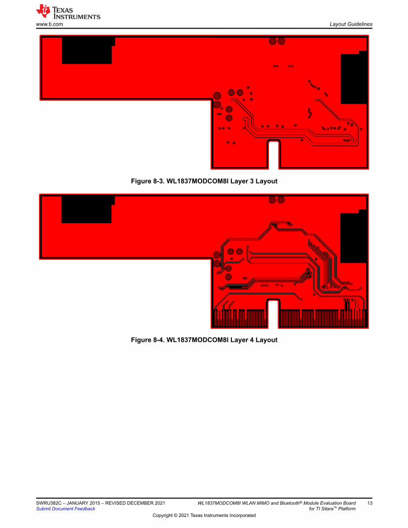
Figure 8-3. WL1837MODCOM8I Layer 3 Layout
Figure 8-4. WL1837MODCOM8I Layer 4 Layout
www.ti.com Layout Guidelines
SWRU382C – JANUARY 2015 – REVISED DECEMBER 2021Submit Document Feedback
WL1837MODCOM8I WLAN MIMO and Bluetooth® Module Evaluation Board for TI Sitara™ Platform
13
Copyright © 2021 Texas Instruments Incorporated
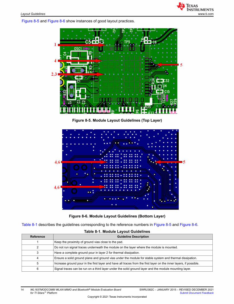
Figure 8-5 and Figure 8-6 show instances of good layout practices.
Figure 8-5. Module Layout Guidelines (Top Layer)
Figure 8-6. Module Layout Guidelines (Bottom Layer)
Table 8-1 describes the guidelines corresponding to the reference numbers in Figure 8-5 and Figure 8-6.
Table 8-1. Module Layout GuidelinesReference Guideline Description
1 Keep the proximity of ground vias close to the pad.
2 Do not run signal traces underneath the module on the layer where the module is mounted.
3 Have a complete ground pour in layer 2 for thermal dissipation.
4 Ensure a solid ground plane and ground vias under the module for stable system and thermal dissipation.
5 Increase ground pour in the first layer and have all traces from the first layer on the inner layers, if possible.
6 Signal traces can be run on a third layer under the solid ground layer and the module mounting layer.
Layout Guidelines www.ti.com
14 WL1837MODCOM8I WLAN MIMO and Bluetooth® Module Evaluation Board for TI Sitara™ Platform
SWRU382C – JANUARY 2015 – REVISED DECEMBER 2021Submit Document Feedback
Copyright © 2021 Texas Instruments Incorporated

Figure 8-7 shows the trace design for the PCB. TI recommends using a 50-Ω impedance match on the trace to the antenna and 50-Ω traces for the PCB layout.
Figure 8-7. Trace Design for the PCB Layout
Figure 8-8 shows layer 1 with the trace to the antenna over ground layer 2.
Figure 8-8. Layer 1 Combined With Layer 2
www.ti.com Layout Guidelines
SWRU382C – JANUARY 2015 – REVISED DECEMBER 2021Submit Document Feedback
WL1837MODCOM8I WLAN MIMO and Bluetooth® Module Evaluation Board for TI Sitara™ Platform
15
Copyright © 2021 Texas Instruments Incorporated

Figure 8-9 and Figure 8-10 show instances of good layout practices for the antenna and RF trace routing.
NoteRF traces must be as short as possible. The antenna, RF traces, and modules must be on the edge of the PCB product. The proximity of the antenna to the enclosure and the enclosure material must also be considered.
Figure 8-9. Top Layer – Antenna and RF Trace Routing Layout Guidelines
Figure 8-10. Bottom Layer – Antenna and RF Trace Routing Layout Guidelines
Layout Guidelines www.ti.com
16 WL1837MODCOM8I WLAN MIMO and Bluetooth® Module Evaluation Board for TI Sitara™ Platform
SWRU382C – JANUARY 2015 – REVISED DECEMBER 2021Submit Document Feedback
Copyright © 2021 Texas Instruments Incorporated

Table 8-2 describes the guidelines corresponding to the reference numbers in Figure 8-9 and Figure 8-10.
Table 8-2. Antenna and RF Trace Routing Layout GuidelinesReference Guideline Description
1 The RF trace antenna feed must be as short as possible beyond the ground reference. At this point, the trace starts to radiate.
2 RF trace bends must be gradual with an approximate maximum bend of 45 degrees with trace mitered. RF traces must not have sharp corners.
3 RF traces must have via stitching on the ground plane beside the RF trace on both sides.
4 RF traces must have constant impedance (microstrip transmission line).
5 For best results, the RF trace ground layer must be the ground layer immediately below the RF trace. The ground layer must be solid.
6 There must be no traces or ground under the antenna section.
Figure 8-11 shows the MIMO antenna spacing. The distance between ANT1 and ANT2 must be greater than half the wavelength (62.5 mm at 2.4 GHz).
Figure 8-11. MIMO Antenna Spacing
Follow these supply routing guidelines:
• For power supply routing, the power trace for VBAT must be at least 40-mil wide.• The 1.8-V trace must be at least 18-mil wide.• Make VBAT traces as wide as possible to ensure reduced inductance and trace resistance.• If possible, shield VBAT traces with ground above, below, and beside the traces.
Follow these digital-signal routing guidelines:
• Route SDIO signal traces (CLK, CMD, D0, D1, D2, and D3) in parallel to each other and as short as possible (less than 12 cm). In addition, each trace must be the same length. Ensure enough space between traces (greater than 1.5 times the trace width or ground) to ensure signal quality, especially for the SDIO_CLK trace. Remember to keep these traces away from the other digital or analog signal traces. TI recommends adding ground shielding around these buses.
• Digital clock signals (SDIO clock, PCM clock, and so on) are a source of noise. Keep the traces of these signals as short as possible. Whenever possible, maintain a clearance around these signals.
www.ti.com Layout Guidelines
SWRU382C – JANUARY 2015 – REVISED DECEMBER 2021Submit Document Feedback
WL1837MODCOM8I WLAN MIMO and Bluetooth® Module Evaluation Board for TI Sitara™ Platform
17
Copyright © 2021 Texas Instruments Incorporated
9 Ordering InformationPart number: WL1837MODCOM8I
10 Revision History
Changes from Revision B (January 2015) to Revision C (December 2021) Page• Updated the numbering format for tables, figures and cross-references throughout the document...................3• Updated language to reflect Bluetooth 5.1 certification...................................................................................... 3• Update was made in Section 2.2........................................................................................................................ 3
Ordering Information www.ti.com
18 WL1837MODCOM8I WLAN MIMO and Bluetooth® Module Evaluation Board for TI Sitara™ Platform
SWRU382C – JANUARY 2015 – REVISED DECEMBER 2021Submit Document Feedback
Copyright © 2021 Texas Instruments Incorporated
IMPORTANT NOTICE AND DISCLAIMERTI PROVIDES TECHNICAL AND RELIABILITY DATA (INCLUDING DATA SHEETS), DESIGN RESOURCES (INCLUDING REFERENCE DESIGNS), APPLICATION OR OTHER DESIGN ADVICE, WEB TOOLS, SAFETY INFORMATION, AND OTHER RESOURCES “AS IS” AND WITH ALL FAULTS, AND DISCLAIMS ALL WARRANTIES, EXPRESS AND IMPLIED, INCLUDING WITHOUT LIMITATION ANY IMPLIED WARRANTIES OF MERCHANTABILITY, FITNESS FOR A PARTICULAR PURPOSE OR NON-INFRINGEMENT OF THIRD PARTY INTELLECTUAL PROPERTY RIGHTS.These resources are intended for skilled developers designing with TI products. You are solely responsible for (1) selecting the appropriate TI products for your application, (2) designing, validating and testing your application, and (3) ensuring your application meets applicable standards, and any other safety, security, regulatory or other requirements.These resources are subject to change without notice. TI grants you permission to use these resources only for development of an application that uses the TI products described in the resource. Other reproduction and display of these resources is prohibited. No license is granted to any other TI intellectual property right or to any third party intellectual property right. TI disclaims responsibility for, and you will fully indemnify TI and its representatives against, any claims, damages, costs, losses, and liabilities arising out of your use of these resources.TI’s products are provided subject to TI’s Terms of Sale or other applicable terms available either on ti.com or provided in conjunction with such TI products. TI’s provision of these resources does not expand or otherwise alter TI’s applicable warranties or warranty disclaimers for TI products.TI objects to and rejects any additional or different terms you may have proposed. IMPORTANT NOTICE
Mailing Address: Texas Instruments, Post Office Box 655303, Dallas, Texas 75265Copyright © 2021, Texas Instruments Incorporated