wireless wearable electrocardiogram (wwecg) final p… · wireless wearable electrocardiogram...
TRANSCRIPT

1
Wireless Wearable Electrocardiogram
(WWECG)
Group 9
Ulbert Botero
Ryan Shifman
Alexander Consunji
Karson Kimbrel

2
Contents 1 Executive Summary ........................................................................................... 7
2 Project Description ............................................................................................ 8
2.1 Project Overview ......................................................................................... 8
2.2 Goals and Objectives .................................................................................. 9
2.3 Requirements ............................................................................................ 10
2.3.1 Physical Requirements ....................................................................... 10
2.3.2 Functional Requirements .................................................................... 11
2.4 Realistic Design Constraints ..................................................................... 12
2.4.1 Economic ............................................................................................ 12
2.4.2 Time .................................................................................................... 12
2.4.3 Ethical ................................................................................................. 12
2.4.4 Health and Safety................................................................................ 13
2.5 Project Operation ...................................................................................... 13
3 Research ......................................................................................................... 13
3.1 Project Motivations .................................................................................... 13
3.1.1 Previous Implementations ................................................................... 14
3.2 Electrocardiography .................................................................................. 15
3.2.1 ECG Overview .................................................................................... 15
3.2.2 Clinical ECG ........................................................................................ 17
3.2.3 The QRS Complex: ............................................................................. 20
3.2.4 Driven Right Leg Circuit ...................................................................... 21
3.2.5 Defibrillator Protection ......................................................................... 22
3.2.6 Arrhythmias: ........................................................................................ 24
3.3 Sampling and Quantization Theory ........................................................... 29
3.3.1 Sampling in Time ................................................................................ 29
3.3.2 Aliasing ............................................................................................... 30
3.3.3 Quantization: ....................................................................................... 30
3.3.4 Oversampling: ..................................................................................... 31
3.3.5 Noise Shaping: .................................................................................... 32
3.4 Wireless Communications ......................................................................... 32
3.4.1 Transmission Standard Comparison ................................................... 32
3
3.4.2 Bluetooth LE 4.0 Overview .................................................................. 33
3.4.3 Local Bluetooth LE Network ................................................................ 33
3.4.3 Processing .......................................................................................... 35
3.4.4 Bluetooth Module Settings .................................................................. 35
3.5 Biomedical Signal Processing ................................................................... 36
3.5.1 Biomedical Signal Processing Applications ......................................... 36
3.6 Electrodes ................................................................................................. 37
3.7 Signal Conditioning ................................................................................... 38
3.7.1 Noise Sources: .................................................................................... 38
3.7.1 Filtering/Noise Reduction: ................................................................... 39
3.7.2 Amplification: ....................................................................................... 39
3.8 Power Management .................................................................................. 40
3.8.1 Rechargeable Battery Technologies ................................................... 40
3.8.2 Charging Circuitry ............................................................................... 40
3.8.3 DC-DC Converters .............................................................................. 41
3.9 Data Converters ........................................................................................ 42
3.9.1 A/D Converters ................................................................................... 42
3.9.2 D/A Converters ................................................................................... 44
4 Standards and Constraints .............................................................................. 45
4.1 Government Regulations ........................................................................... 45
4.1.2 Radio Frequency Devices FCC ........................................................... 45
4.2 Bluetooth LE Hardware Constraints .......................................................... 45
4.2.1 Range ................................................................................................. 46
4.2.2 Transmitters needed for each Device ................................................. 46
4.2.3 Latency ............................................................................................... 46
4.2.4 Data Rate ............................................................................................ 46
4.3 Bluetooth Software Security Standards ..................................................... 46
4.4 Testing Constraints ................................................................................... 47
5 Design Plan ..................................................................................................... 47
5.1 Electrode to Electrode Sampling Synchronization ..................................... 50
5.1.1 Timestamping ..................................................................................... 51
5.3 Firmware and Software Plan ..................................................................... 52
4
5.3.1 Electrode Sensors ............................................................................... 53
5.3.2 Hub ..................................................................................................... 55
5.3.3 Android Application ............................................................................. 56
5.4 Hub Receiver and External Processing ..................................................... 59
5.4.1 Post-Transmission Preprocessing ...................................................... 59
5.4.2 Digital Signal Processing Algorithms for ECG signal .......................... 59
5.5 ECG Signal Requirements ........................................................................ 64
5.6.1 Leads .................................................................................................. 64
5.6.2 Bandwidth ........................................................................................... 65
5.6.3 Gain .................................................................................................... 66
5.6.4 Resolution ........................................................................................... 67
5.6.5 Common Mode Rejection Ratio .......................................................... 68
5.7 Signal Acquisition Stage ............................................................................ 68
5.7.1 Anti-Aliasing ........................................................................................ 68
5.7.2 Noise Filtering ..................................................................................... 71
5.7.3 Amplification ........................................................................................ 73
6 Parts and Hardware ......................................................................................... 75
6.1 Operational Amplifiers ............................................................................... 75
6.1.1 Pin Configuration................................................................................. 75
6.2 DC-DC Converters .................................................................................... 76
6.2.1 Pin Configuration................................................................................. 76
6.3 Texas Instruments TMS320C5535 DSP ................................................... 77
6.3.1 Central Processing Unit ...................................................................... 77
6.3.2 Internal Memory .................................................................................. 77
6.4 Instrumentation Amplifier ........................................................................... 78
6.4.1 Texas Instruments INA333 .................................................................. 78
6.5 Bluetooth Module HM-11 with a Texas Instruments CC2541 .................... 80
6.6 Data Converters ........................................................................................ 80
6.6.1 Analog to Digital Converter ................................................................. 80
6.7 Digital to Analog Converter ....................................................................... 84
6.7.1 Texas Instruments DAC8411: ............................................................. 84
6.8 Microcontrollers ......................................................................................... 86

5
6.8.1 Wrist Mounted Microcontrollers ........................................................... 87
6.8.2 Central Hub Microcontroller ................................................................ 88
7 Software Applications and Database ............................................................... 90
7.1 WWECG Server Specifications ................................................................. 90
7.1.1 The Database ..................................................................................... 91
7.1.2 The Application Programming Interface .............................................. 95
7.3 WECG Client Specifications .................................................................... 113
7.3.1 Screens ............................................................................................. 113
7.3.2 Custom UI Components .................................................................... 117
7.3.3 WWECG Bluetooth Link .................................................................... 117
7.3.4 WWECG Server Link ........................................................................ 117
7.3.5 WWECG Live Processing ................................................................. 117
7.4 Storage .................................................................................................... 118
8 Administrative Information ............................................................................. 118
8.1 Project Management Methodology .......................................................... 118
8.2 Material Cost Analysis ............................................................................. 118
8.3 Facilities and Equipment ......................................................................... 119
8.4 Personnel ................................................................................................ 119
8.5 Past Activity Levels ................................................................................. 120
8.6 Future Milestone Chart ............................................................................ 125
9 Construction and Testing ............................................................................... 128
9.1 Chipset Integration .................................................................................. 128
9.2 PCB Design ............................................................................................. 129
9.3 PCB Manufacturing ................................................................................. 129
9.4 ECG Signal Quality ................................................................................. 129
9.5 Level of Comfort ...................................................................................... 129
9.6 Testing Procedures ................................................................................. 130
9.6.1 Hardware Testing .............................................................................. 130
9.6.2 Software Testing ............................................................................... 131
10 Conclusion ................................................................................................... 131
11 APPENDIX A- Copyright Permission ........................................................... 133
12 APPENDIX B- References........................................................................... 134

6
13 APPENDIX C- Data Sheets and User Guides ............................................. 136
7
1 Executive Summary
The ECG (Electrocardiogram) has been an invaluable tool to healthcare
professionals since the early 1900s. Since its inception, many advances in
technology have taken what was once a bulky laboratory instrument and turned it
into the compact portable piece of equipment we know today. Our design project
will further advance the ECG into a wireless wearable device for personal and
professional health care use.
Today we find that the need for digital data to be easily accessible is a growing
demand in the medical field. Our design will allow the user to act in a dynamic
environment without the same constrictions as a conventional leaded ECG. The
wireless transmission of data from our device will free the user to move about
without the hindrance of wired leads from the ECG. This will also provide the
healthcare professional the convenience of monitoring a patient’s health without
the need of being in the same room.
The WWECG (Wireless Wearable ECG) will use medical grade disposable
electrodes that snap onto the device to pick up the electrical potential changes of
the skin caused by heart’s cardiac cycle. This signal will be riddled with noise so
before it can be of any use it must be filtered to drown out any unwanted signals.
We have decided that a combination of both analog and digital filtration will provide
us a signal with the best fidelity. By using a series of analog filters the signal will
be conditioned to drown out noise produced by mains hum (a 60 Hz electrical noise
coming from power lines), motion artifact noise, and baseline drift. Once this signal
has been digitized, a digital signal processor will use separate algorithms to adjust
the signal shape, QRS wave, calculate heart rate, and detect ventricular
arrhythmia.
The user will access this data through an app on their phone or tablet that will
connect with our system using Bluetooth. The app will be developed for Android
devices and will display the data gathered by our system to the screen of the
device. The signal will be available to display in real time and the app will also keep
a record of signals for a select period of time. Several modes of operation will be
available such as a display of the ECG signal along with user heart rate. The app
will provide an easy to use experience for the user whether they are a healthcare
professional or a patient.
To develop this type of design it is necessary to research current and previous
techniques used in both modern and outdated ECGs to understand what areas
have been improved upon and what areas still need improvement. Consulting
medical professionals and engineers with experience in the biomedical
engineering field will be necessary in achieving the highest accuracy for our
design. In creating a precise and accurate device to record heart activity we hope
to expand the use of the ECG to broader fields as well. Our intent is to make the

8
WWECG an integral part of tracking trends by providing the most accurate data
possible for the user.
2 Project Description
With new innovative healthcare devices being integrated into the professional
healthcare environment every year, the methods that doctors use to monitor
patient’s vitals are continuously changing. As medical equipment moves towards
preventative healthcare the need for smaller and portable handheld devices
increases. The WWECG will provide the solution for these needs by reducing size
and increasing accuracy with low power consumption communications and a mix
of analog and digital processing. Advances in fabrication of chip size will be our
biggest advantage in developing a smaller more compact diagnostic device than
we have seen in the market.
Our design will take the analog signal from the body and convert it into digital data
to be sent wirelessly over Bluetooth to be processed by an external processing
unit. This processing unit will then send that processed data wirelessly over
Bluetooth to an Android based mobile app that can be accessed through any
Android device. The app will provide the user with an easily accessible display of
their ECG signal.
2.1 Project Overview
Figure 2.1 below shows the block diagram that our system will follow. The signal
will be obtained from two electrodes placed on the body and will then be filtered
through a low pass filter with a 3 dB cutoff of 100 Hz for diagnostic purposes and
a high pass filter with a 3 dB cutoff of .5 Hz to remove the noise caused by motion
artifacts. A notch filter will remove the 60 Hz noise of the signal contributed by
power lines. The amplification stages for each signal path will consist of operational
amplifiers with gain stages adding up to a total gain of 1000. Such high gain is
necessary for the signal to be converted to digital data as the initial signal obtained
from the body is in the range of millivolts while the analog to digital converter’s
input range is read in volts.
The conversion of analog to digital data will allow the signal to be sent wirelessly
by a low power Bluetooth module to be processed by an external processing unit.
The external processing unit will utilize a digital signal processor to further
condition the signal using algorithms to reduce noise and improve signal shape,
detect ventricular arrhythmia, and identify QRS complexes. The android and web
app portion will deal with the recording and display of user data.
The WWECG system will utilize lithium ion technology to make it a portable and
rechargeable product. Advancements in lithium ion polymer technology have

9
reduced the size of rechargeable battery packs allowing for the reduction of the
charge management portion of our design. This reduction in size will greatly
contribute in our attempt to keep our system small and wearable while still having
the capability of being rechargeable, thus eliminating the waste of having to recycle
conventional batteries.
Figure 2.1 – System Block Diagram
2.2 Goals and Objectives
The overall objective of this project is to create a fully functional ECG completely
wirelessly, while there have been many ECGs on the market that utilize newer

10
wireless technologies like Bluetooth and Wi-Fi, there is currently no market
implementation of a completely wireless that features two electrode sensors that
are not connected together with physical wires. Our current design aspirations
feature this by transmitting all necessary data with Bluetooth in order to fix this
problem. By having two separate electrodes it allow whomever the current user is
to move both arms freely by using wrist mounted sensors. Overall while
constructing this project the following goals the project looks to output is the
following,
1. A completely hands-free wrist mounted implementation of a rhythm strip that
would normally be produced by an Electrocardiogram.
2. An active mobile application that stores and displays the user’s data for them to
interpret and utilize as needed.
3. Run for an extended period of time of at least an hour.
4. Have a simple and easy to use interface system in regards to both software and
hardware.
5. Make the device comfortable enough to wear allowing the user a completely
hands free range of motion.
6. Display a high resolution image of the user’s data in graphical format similar to
a professionally made ECG.
7. Notify the user of any possible problem that may be occurring within the heart
arrhythmia, atrial fibrillation etc.
By meeting all of these goals, the WWECG will be one of the first full wireless
implementations of an Electrocardiogram, and will be able to help detect various
heart problems that can only be detected by a standard ECG.
2.3 Requirements
A total combination of all the subset requirements listed below will result in the
overall needs for the project above. In order to meet the project goals seen above,
these requirements need to be met fully and in conjunctions.
2.3.1 Physical Requirements
For the WWECG the overall physical requirements that need to be met in order to
meet the project goals can be seen below within Table 2.3.1. As show in the table
these requirements help determine the physical limits and capabilities of the
WWECG while also working around the hardware constraints imposed.

11
Dimensions 50mm x 50mm x 15mm (LxWxH) for the wrist mounted electrodes. 200mm x 100mm x20mm (LxWxH) for the hub for data transmission.
Power and Transmitter Runtimes
Lithium-Ion polymer with Micro USB Charging 1 Hour Runtime
Weights Each Electrode with transmitters 16gs
Operating Conditions 10-40C 25-75% humidity
Storage Conditions -20 - 50C 25-75% humidity
ECG Channels 2 Channels
Frequency .1 to 50hz
Sampling rate 200 samples per second
Sampling Resolution 16 Bit
Table 2.3.1 –Physical Requirements
2.3.2 Functional Requirements
The table below in Table 2.3.2 displays the overall functional requirements that
need to be completed in order to achieve a proper method of performance
throughout the WWECG.
Physical Functionality
-Simple clean physical interface that allows user easy access to all necessary points as well as notification LEDs. -Device should be sleek and comfortable when worn for at least an hour.
Software Interface
-Visual Display showing the full rhythm strip. -Simple user menu and access in order to view past readings. -Able to store data from multiple sessions of readings to serve and compare data from remote server to current reading. -Detection for ECG recognizable heart symptoms. -Must comply with HIPAA requirements.
Server Interface -Ability to store and access data upon user requests. -Must comply with HIPAA requirements.
Table 2.3.2 –Functional Requirements

12
2.4 Realistic Design Constraints
The current design constraints for the project are due to the following sections
below, Economic, Time, Ethical, Health and Safety constraints. Due to these
subjects the capabilities of this project will be limited to a proof of design concept
that could possibly be used in commercial application.
2.4.1 Economic
The main economic constraint within this product revolves around the fact that it is
currently without any forms of sponsorship which limits the amount of testing
mechanisms available to use for testing and parts. With the need for the highest
quality parts possible while also maintaining within the current budget of four full
time students being a key factor in our choice of parts as well as our testing
material, the current economical state is a large contributing factor to the product
accuracy. With this product accuracy needing to only meet commercial standards
rather than medical, the project is still capable of being produced by sacrificing
some unnecessary features that would add cost to the project.
2.4.2 Time
Another extremely large factoring into the design and implementation of the project
regards the limited amount of time available for each member of the group. With
all of the members of the group having other tasks and commitments throughout
the projects construction, the given amount of time limits the amount of features
that the project will be capable of. While the WWECG will still have all of its overall
base hardware aspects, to mimic a full ECG in a medical testing sense would
require not only multiple months to years of testing on top of our previous design,
but also would require many more electrodes that would add another layer of
complexity to the project in both design and simulation. With a fully functional ECG
consisting of at least 12 nodes attached to the body at a given time to be used for
medicinal purposes, the capabilities of our project creating and having a properly
functioning device would be extremely unlikely given the current time constraints
of the project.
2.4.3 Ethical
The key ethical constrain when developing this project is during the testing for the
device without using people or animals. In order to overcome this problem, testing
will be done using an ECG simulator which will allow for unlimited testing without
violating a domestic or international human testing standards since the entirety of
human testing will be ignored.
13
2.4.4 Health and Safety
For this project the key constraints with the health and safety regard safely allowing
the user of the device to use it for an extended period of time comfortably without
there being electrocuted while wearing the WWECG. Another concern regarding
the health and safety is to not burn the user in case of defibrillator use while
wearing the device. So when developing the device these two constraints need to
be kept in mind. Another important constraint is the need for encrypted data
whenever it is transmitted from device to device in order to protect the user’s data
from outside unwanted access.
2.5 Project Operation
The Wireless Wearable Electrocardiogram is a wearable health-monitoring device that will provide its user with an accurate display of heart activity, heart rate, and warn of arrhythmia detections. All of this information will be displayed to the user via an android mobile application. The WWECG consists of two wrist sensors that serve to calculate Lead 1 for heart activity. First you attack the electrode clip to a location on the user's body. For this example the wrist is commonly used as the location of each electrode. Each sensor then acquires the biopotential signal and conditions it to be digitized and transmitted wirelessly via Bluetooth LE to the Hub. The Hub is both a docking/recharging station for the sensors and serves to complete the processing of the signal. Specifically, the Bluetooth LE transmitted signals are received at the hub and then passed into an instrumentation amplifier to produce the desired electrocardiogram signal. This signal is then converted to digital and further cleaned up in the digital signal processor. Additionally, it is here where the algorithms to detect the QRS complex of the waveform, the user's heart rate, and detection of any arrhythmias are implemented. The data will be transmitted continuously while the hub is in operation and the user's mobile application is connected to the hub via Bluetooth. Now the user will open the application on their mobile device and log into their created account. Once logged in they can view a real time display of their heart rhythm activity, with markings of where the QRS complex is occurring, along with a display of their heart rate. Furthermore, this application will notify the user if any arrhythmic behavior has been detected.
3 Research
This section discusses our research findings that guided our design approach.
3.1 Project Motivations
Overall the group motivation for this project comes down to a desire to learn more
about signal processing, biomedical engineering uses electronics, wireless

14
transmission data transfers and client server applications using an Android device
and communicating with a separate hardware entity from a singular application.
The main motivation for moving towards a more biomedical engineering in
combination with our already more well versed fields of study is the desire to
familiarize ourselves with the field’s various aspects that vary and are similar to
what we have learned throughout our undergraduate careers. The main reason
that the project was decided to move towards an ECG was due to not only interest
in cardiology itself, but it also provides valuable knowledge on how to take readings
from wrists mounted devices which is currently popular with fitness companies.
Feeling that these experiences could give us an edge when entering the workforce
while also desiring to work towards a newer more innovative project, it was
determined that a wireless wearable device would be best suited for a Senior
Design project.
3.1.1 Previous Implementations
While researching various implementations of ECGs and wireless transmitters, a
few different wireless ECG models were discovered featuring designs similar to
WWECG but still maintaining an underlying wiring to determine the timing
difference between both electrode sensors.
3.1.1.1 MIT Thesis
During our overall design and planning stages of the project was a Master’s thesis
paper by Margaret Delano from MIT proved to be one of the best references
possible. Developing a wearable Electrocardiogram monitor, there was not only a
concise and accurate representation of her design and implementation, but also
an extremely descriptive and accurate representation of ECGs and their uses from
an electrical engineering perspective. Providing many helpful resources of
commercial implementations that have already been done, there were also many
helpful descriptions about various implementations that were not originally
considered within our design plan. Providing the complete overview from design
to implementation along with the various errors encountered when designing and
creating the project, the document also will allow us to recover from many
challenges that would have likely occurred during this WWECG implementation.
Overall this this proved to be an extremely helpful document during each stage
that have been completed so far as well as the development plans in the future.
3.1.1.2 Qardio
Another one of the current implementation of a wearable ECG on the market is
called the QardioTM. It features a four electrode module that is mounted on the
chest rather than the wrists and uses dry electrodes as well rather than wet. Similar
15
to other designs that have already been developed this implementation hides the
wiring between electrodes instead of having a completely wireless implementation.
3.2 Electrocardiography
Before implementing any signal processing algorithms to describe and detect heart
behavior it is important to understand what it means. Therefore, it is necessary to
first gain an understanding of the heart and body's operation as an electrical
system. The heart is made up of the myocardium muscle that rhythmically
contracts and drives circulation of blood throughout the human body. Before every
heartbeat an electrical current is passes through the entire heart and triggers
myocardial contraction. This event is referred to as a systole. The electrical waves
propagate over the structure of the heart in a coordinated pattern that leads to a
coordinated systole. This allows for a measurable change in potential difference
across the surface of the body. This potential difference can then be amplified and
filtered to produce the popular electrocardiogram signal known today. The ECG
signal has a wide range of factors that can affect its behavior. These include
abnormalities in the cardiac conducting fibers, metabolic abnormalities of the
myocardium, and macroscopic abnormalities of the heart's geometry.
3.2.1 ECG Overview
The next two sections give a brief overview of the main processes that occur
within the ECG.
3.2.1.1 ECG Cellular Processes
Every heartbeat is triggered by an action potential that originates from a rhythmic
pacemaker in the heart which produces a coordinated contraction after being
conducted rapidly throughout the organ. The myocardial cell typically has a resting
membrane potential, Vm, of approximately -80 to -90 mV with respect to its
surrounding extracellular fluids. The cell membrane controls the permeability of
different ions such as, sodium, potassium, calcium, and chloride. This permeability
is responsible for the ions being able to pass across the membrane via opened
and closed ion channels. Furthermore, these gated channels open and close as a
response to voltage changes in the voltage gated channels or the activation of
receptor gated channels. The variation of conductance in the membrane due to
the opening and closing of the ion channels generates changes in the action
potential. There are five conventional phases that the cell goes through during
depolarization and repolarization. First, the cardiac cells are depolarized to the
threshold voltage of -70mV. Phase 0 to phase 1 consists of the depolarization
caused by a transient increase in fast sodium channel conductance. Then phase
1 is the repolarization of the cell caused by the opening of the potassium channel.
16
At phase 2 there is now a balance between the incoming calcium current and
outgoing potassium current that causes a plateau in the action potential and delay
in repolarization. Repolarization then occurs in phase 3 due to an increase in
potassium conductance. Additionally, repolarization occurs because a decrease in
calcium conductivity occurring at the same time. The last phase (phase 4) acts as
the resting phase and consists of open potassium ion channels and a negative
membrane potential.
Cardiac cells that possess the property of automaticity, known as pacemakers, are
critical to action potential propagation. They have the ability to spontaneously
depolarize and this property allows them to behave as pacemakers for the rest of
the heart. These cells are found in the sino-atrial node, atrio-ventricular node, and
in some specialized conduction systems within the atria and ventricles. In
automatic cells, the resting potential is not stable and shows spontaneous
depolarization. Once the cell's potential reaches a threshold level the cell then
develops an action potential that is mediated by calcium exchange at a very slow
rate. After the action potential the cell then returns back to its resting phase and
the cycle repeats. There are graded levels of automaticity of the heart that are
directly related to heart rate. For example, the SA node's (sino-atrial) rate is the
highest around 60-100 beats per minute, followed by the AV(atrio-ventricular) at
approximately 40-50 bpm, and then the ventricular muscle at about 20-40 bpm.
Once an action potential is initiated in a cardiac cell it will continue to propagate
throughout the cell until the entire cell is depolarized. The action potential is spread
throughout the myocardial cells due to their unique ability to transmit action
potentials from cell to adjacent cells via direct current spread. The cell membranes
are tightly coupled and this allows them to transmit the tension and electric current
from cell to cell. Furthermore, the ionic currents flow from cell to cell via low
resistance gap junctions and this allows the heart to behave electrically as a
syncytium. Therefore, an impulse that originates anywhere in the myocardium will
propagate through the heart and produce a coordinated mechanical contraction.
In addition to the action potential propagating via the myocardium, it can also
propagate via bands of specialized conducting fibers. By traveling across
combinations of both methods the action potential is able to propagate to all the
regions of the ventricles.
3.2.1.2 Physical Basis behind ECG
We are able to measure the potential differences on the skin's surface and current
that flows within the body due to the electrical activity of the cells. The graphical
representation of these potentials plotted as a function of time are the popularly
known Electrocardiogram. The most popular mathematical model used to relate
the body surface potentials to the electrocardiogram signal is the single dipole
model. This model has two main components, the dipole that acts as a

17
representation of the heart's electrical activity, and the geometric and electrical
properties of the surrounding body. First, the electrical activity of the heart is
considered. As an action potential propagates throughout a cell it generates an
intracellular current as well in that same direction. This is the basic source of the
surface electrocardiogram and is referred to as the current dipole. In contrast, there
is an equal extracellular current that flows in the opposite direction or propagation
that conserves charge. These current loops close upon themselves and form a
dipole field.
The net equivalent dipole moment is referred to as the time-dependent heart vector
M(t). This is based on the assumption that if the heart were observed in a
homogenous isotropic conducting medium at a distance large compared to its size,
then all the current dipoles can be assumed to originate at a single point. Then the
total electrical activity in the heart can be depicted as a single equivalent dipole
whose magnitude and direction is the vector total of all the smaller poles. The heart
vector changes with respect to magnitude and direction as each wave of
depolarization occurs. The current and potential distributions depend on the
electrical properties of the torso and approximating the dipole model as a linear,
isotropic, homogenous, spherical conductor with radius, R, and conductivity, 𝜎
.The static electrical field, current density, and electrical potential all along the torso
are related to the heart vector as a quasi-static model. Based on the assumptions
above the potential distribution of the torso can be represented by
𝜑(𝑡) = 𝑐𝑜𝑠𝜃(𝑡)3|𝑀(𝑡)|
4𝜋𝜎𝑅2
where 𝜃(𝑡) represents the angle between the direction of the heart vector M(t) and
the lead vector, OA. OA represents the center of the sphere, O, joined to the point
that is being observed, A. The potential difference between two points on the
surface can be generally related by the equation
𝑉𝐴𝐵(𝑡) = 𝑀𝑡) ∗ 𝐿𝐴𝐵(𝑡)
and LAB is the lead vector on the torso connecting points A and B. Lastly, a central
terminal(CT) is determined by averaging the potentials across the three limb leads,
right arm(RA), left arm(LA), and left leg(LL). This central terminal acts as a
reference and should be zero at all times.
𝜑𝐶𝑇(𝑡) = 𝜑𝑅𝐴(𝑡) + 𝜑𝐿𝐴(𝑡) + 𝜑𝐿𝐿(𝑡)
3.2.2 Clinical ECG
The clinical ECG is based on a number of factors but mainly on the contraction
and relaxation properties of the myocardium. The heart has four cavity chambers
with walls that consist of mechanical syncytium of myocardial cells. There is a valve
that closes after each contraction at the exit of each chamber. This serves to
18
prevent retrograde flow while the chamber relaxes and the downstream pressure
exceeds the pressure within the chambers. The right heart has a small atrium that
leads into a larger right ventricle. This right atrium receives blood from the body
and flows it into this right ventricle. The right ventricle then contracts to push the
blood into the lungs, where it is oxygenated and carbon dioxide is removed. The
left atrium behaves similarly by conducting blood into the left ventricle but instead
of propelling the blood into the lungs it pushes it through the aorta to the rest of the
body.
Additionally, there are nine different temporal states that relate to the trajectory of
heart vectors. Atrial depolarization is when the wave of depolarization flows
throughout both atria and the summation vector is pointing down, to the subject's
left, and anterior. The next state involves the delay at the AV node. During this
delay there is no electrical activity that can be measured as a surface potential
unless special techniques are used. Afterwards, activity emerges from the AV node
and depolarizes the His bundle and the bundle branches directly after. Next is
septal depolarization. During this state as the action potential enters the septal
myocardium the wave propagates from left to right and the resulting heart vector
points to the subject's right. Apical depolarization is when the wave of
depolarization moving left is balanced by the ave moving right. This results in the
heart vector pointing towards the apex of the heart. Left ventricular depolarization
and late left depolarization both consist of electrical activity in the right ventricle but
the activity in the left ventricle dominates. Once the various portions of the
myocardium depolarize, they begin the excitation-contraction process. Then there
is a period where the myocardium depolarizes and no action potential propagates,
which results in no measurable cardiac vector at this point. Finally, the cells begin
to repolarize and a wave of charge passes through the heart. This charge
originates from depolarizing and repolarizing tissues. Afterwards, the heart returns
to a resting state and awaits another electrical stimulus to restart the cycle.
Lastly, the clinical ECG is based on the cardiac vector, which expands, contracts,
and rotates in three dimensional space, and is projected onto 12 different well
defined directions. These 12 orientations are the basis behind the common 12 lead
configuration. Each lead represents the magnitude of the cardiac vector in that
direction at each instant in time. Typically, there are six leads placed around the
torso and the ECG signal will represent the difference between the specific leads
and the central terminal discussed earlier. Furthermore, there are four additional
limb leads attached to the patient. The potential differences between the
combinations of limb leads results in the remaining clinical ECG leads. Lead 1 is
the potential difference between the left arm and right arm. Lead 2 is the potential
difference between the left leg and right arm. And the potential difference between
the left leg and left arm results in lead 3. These leads are often referred to as the
Einthoven Limb leads (bipolar).

19
Figure 3.2.2: Einthoven's Triangle
𝐿𝑒𝑎𝑑 1: 𝑉1 = 𝜑𝐿𝐴 − 𝜑𝑅𝐴
𝐿𝑒𝑎𝑑 2: 𝑉2 = 𝜑𝐿𝐿 − 𝜑𝑅𝐴
𝐿𝑒𝑎𝑑 3: 𝑉3 = 𝜑𝐿𝐿 − 𝜑𝐿𝐴
The right leg is typically used as a ground reference electrode in most clinical
electrocardiograms. Additionally, the three limb leads are typically sufficient for
determining the heart's rhythm. In addition to the Einthoven limb leads the
augmented limb leads can represent the potential at a given limb with respect to
the average of the other two limb's potentials. Augmented limb leads are denoted
by "a", such as aVR, which is the difference to between the right arm and the
average of the left arm and left leg leads. The other augmented leads are aVF,
difference between left leg and average of right arm and left arm, and aVL, the
difference between the left arm and average of the right arm and left leg potentials.
Due to using twelve leads to image three dimensional space some information may
be redundant but this is still helpful for aiding in human interpretation of the heart's
behavior as well as helping to account for minor errors in electrode placements.
This is often referred to as spatial oversampling.

20
3.2.3 The QRS Complex:
The QRS complex refers to the combination of three of the most prominent
deflections seen on the ECG. It typically corresponds to when the right and left
ventricles of the heart are in the depolarization state. The clinical significance of
the QRS complex is that it provides a useful method of diagnosing cardiac
arrhythmias, conduction abnormalities, ventricular hypertrophy, and other types of
disease states. For example, a conduction abnormality would be able to be seen
directly because it would widen the QRS complex. In addition, the QRS complex
is typically used to determine the electrocardiogram's axis. Commonly, the ECG
has five deflections that correspond to the P, Q, R, S, and T components of the
ECG signal. A Q wave is any downward deflection that occurs after the P wave.
An R wave then follows this Q wave but as an upward deflection instead. And the
S wave is the following downward deflection following the R wave. The Q wave
represents the depolarization of the interventricular septum, which is the wall that
separates the lower chambers of the heart from one another. When the electrical
signal passes through a scarred heart muscle it is referred to as a pathologic Q
wave. Pathologic Q waves are typically used as markers for previous myocardial
infarctions (heart attacks). The R wave is represented differently depending on the
lead it is measured from. With respect to lead V1 the rS complex typically shows
an increasing R and decreasing S when moving towards the left. In leads V5 and
V6 the R-wave amplitude is taller in V5 than V6. The transition zone occurs in leads
V3 or V4. During this period the QRS complex changes from being mostly negative
to being predominantly positive. It isn't uncommon for this transition zone to also
appear earlier at V2 or later at V5. The R wave is an important indicator in signal
processing and biomedical engineering. In biomedical engineering the maximum
amplitude of the R wave is often referred to as the R peak amplitude or just R peak.
And the accurate detection of the R peak is essential in heart rate measurement
and arrhythmia detection signal processing algorithms. Poor R wave progression
is when the R wave is less than 2-4 mm in leads V3 or V4 and/or an occurrence of
a reversed R wave progression, and it is commonly attributed to heart attacks as
well. Lastly, the J-point is the location where the QRS complex meets the ST
segment. It is typically the first point of inflection for the upstroke of the S wave and
where the ECG trace becomes more horizontal than vertical.

21
Figure 3.2.3. : Typical QRS complex in Electrocardiogram Signal
3.2.4 Driven Right Leg Circuit
The driven right leg circuit is a common circuit employed in electrocardiograms and
other biological signal amplifiers. Its main purpose is to aid in reducing the
common-mode noise often seen at electrode inputs. The body often acts as an
antenna which picks up electromagnetic interference, mainly the 50/60 Hz noise
from electrical power lines. This noise tends to be a much higher amplitude than
the desired biopotential signal which makes it much harder to measure those
desired signals. Another common source of noise is the Common-mode to
differential mode conversion. Due to mismatches in electrode impedances it’s
common that some common-mode voltage sneak into the differential voltage of
the instrumentation amplifier. The driven right leg circuit aids in eliminating these
noise issues by using the two typical limb leads, instrumentation amplifier, and a
third driven electrode. The added circuitry measures the common mode voltage
between the two electrodes and negatively amplifies the output. The body is then
driven to that potential because it is tied to the circuit common. This effectively
drives any power line noise back into the body as well. By driving these signals
back into the body it is effectively minimizing the amplitude of these signals and
makes it easier to measure the desired ECG signal. Additionally, this circuit helps
increase patient safety. If a high voltage were to appear between the patient and
ground then the auxiliary op amp attached to the patient on the right leg would
saturate. This saturation causes the op amp to no longer be able to drive the right

22
leg and ungrounds the patient. A large resistor between the patient and ground,
normally on the order of Mega ohms, is normally large enough to protect the user.
Figure 3.2.4 Right Leg Driven circuit - Permission Pending
3.2.5 Defibrillator Protection
The purpose of our wireless wearable electrocardiogram medical device is to
provide a safe and convenient method of measuring the user's heart rhythms.
Often the device itself will not provide any electrical risk to the user but there are
instances that the opposite is true. Specifically, when a defibrillator is used on a
patient it presents a risk to the electronics of the monitoring device due to the high
voltage applied to the human body through the defibrillators. It is possible that the
high voltage could be transferred from the leads attached to the patient into the
ECG sensors. Therefore, the purpose of the defibrillation protection circuit is more
to protect the electronics of the device from an abnormally high voltage pulse than
the patient. It is most important for the circuit to limit the voltage and current that
can be transmitted to the device. There are mainly two commonly implemented
methods for voltage limiting, using voltage suppression diodes and gas lamps/gas
discharge tubes. And series resistors are often employed to limit the current.
3.2.5.1 Transient-Voltage-Suppression
Transient-Voltage-Suppression diodes (TVS Diodes) are very useful electronic
components that mainly serve to protect sensitive electronics from sudden voltage
spikes. They operate by shunting excess current when the voltage surpasses the
avalanche breakdown voltage of the device. Then clamping the voltage by
suppressing all voltages that are greater than its breakdown voltage. Afterwards,
once the abnormally large voltage has subsided the device automatically resets

23
and absorbs a large amount of the transient energy internally. TVS diodes can be
either unidirectional or bidirectional. Unidirectional TVS diodes mainly act as
forward direction rectifiers that can handle higher peak voltages than other
avalanche diodes. Bidirectional TVS diodes typically are represented by two
mutually opposing avalanche diodes that are in series with each other and
connected in parallel to the circuit that they are protecting. An advantage of TVS
diodes is that they are able to respond to over-voltages much faster than other
typical voltage suppression components like varistors or gas discharge tubes.
They tend to operate and clamp the voltages within 1 picosecond. However, there
are three instances for which the TVS diodes will fail. A short in the circuit, open
circuit, or a degraded device. If subjected to conditions that it wasn't designed to
accommodate the TVS diode will most likely fail.
3.2.5.2 Gas Discharge Tubes:
Gas discharge tubes are another commonly implemented method of voltage
suppression, especially in Electrocardiogram front end circuitry protection.
Specifically, gas discharge tubes are an arrangement of electrodes in a gas that
are within an insulating, temperature resistant envelope. These tubes exploit the
behavior of electric discharge specific to when it is within a gas. They operate by
discharging in the gas with an applied voltage that is enough to cause electrical
conduction based on the principles of the Townsend discharge. Specifically, this
process occurs when free electrons in a gas are accelerated by a strong electric
field and leads to conduction within this gas by avalanche multiplication, similar to
avalanche breakdown in TVS diodes. Once the number of free charges decreases
or the incidental electric field weakens the process will cease. The voltage required
to begin and hold the discharge of the gas tube depends on the composition and
pressure of the gas within the tube, as well as the geometry of the tube. Different
types of gases have different applications when implemented in gas discharge
tubes. For the purpose of voltage regulation for electronics protection neon glow
tubes are typically employed.
3.2.5.3 Electrostatic Discharge Protection:
Another potential risk to the electronic monitoring device is electrostatic discharge.
Medical devices like the Wireless Wearable Electrocardiogram often have patients
and medical professionals handling the device. This high amount of frequent
contact presents the opportunity for a simple static discharge to enter the device
and harm the electronics. To protect from ESD space-efficient semiconductor
based devices such as Zener diodes are most often employed.

24
3.2.6 Arrhythmias:
A key feature of the wireless wearable electrocardiogram will be implementing an
arrhythmia detection algorithm in the digital signal processing portion of the device.
This is an important feature because it will allow for the user, whether it be a
physician or someone using it for fitness tracking, to be warned once an arrhythmic
breathing pattern has been detected. Before implementing such an algorithm it is
important to understand what arrhythmias actually are and the different types of
them.
An arrhythmia is any irregularity occurring in the patient’s sinus rhythm. An
arrhythmia is typically associated with electrical instability and abnormal
mechanical cardiac behavior. Additionally, most arrhythmias are categorized by
the locations the electrical abnormalities originate from. For example, atrial flutter
is a type of arrhythmia that occurs in the atria of the heart. Arrhythmias can be
diagnosed due to a variety of conditions. They can consist of isolated abnormal
beats, sequences of abnormal beats mixed with regular beats, or exclusively
abnormal beats. The severity of arrhythmias vary based on how much they
interfere with the hearts normal activity. Isolated beats tend to not be worrisome
because they don't interfere with normal cardiac behavior too much. However, it is
an indication that there may be an underlying pathology in the cardiac tissue. Sinus
rhythms that are predominantly abnormal are much more problematic. Most are
easily handled with medication but others can be fatal if they aren't handled
immediately.
Arrhythmias are mainly caused by non-pacing cells acting like pacemakers, and is
known as reentry. Reentry is due to a conduction pathway loop that contains a
region of blocked conduction and a region of slowed propagation. When the action
potential reaches its point of origin it comes in contact with excitable tissue and
causes an oscillation around the loop at least once. Reentry can occur in multiple
locations within the heart, such as the atria or ventricles of the heart. In fact, it is
important to distinguish between arrhythmias occurring in either region. Atrial
arrhythmias rarely are severe or life threatening. They mainly result in minor issues
such as palpitations, weariness, or decreased exercise tolerance. But ventricular
arrhythmias very severe and life threatening if not handled immediately.
3.2.6.1 Types of Arrhythmias
There are multiple types of arrhythmias that vary greatly from one another. This
section discusses a brief overview of their most prominent distinctions.

25
3.2.6.1.1 Atrial Flutter
Atrial flutter is caused by a reentrant rhythm that occurs in either the right or left
atrium. An electrical impulse prematurely arises in the atria and the differences in
tissue properties then cause a loop of reentry moving through the atrium. Atrial
flutter is normally associated with an elevated heart rate of more than 100 beats
per minute. Typically this condition occurs in individuals with cardiovascular
diseases and diabetes mellitus, but it can occur in people with normal hearts as
well. Although those cases tend to be more spontaneous and not long lasting.
Rarely does atrial flutter persist for months to years. The main worry with atrial
flutter is that it frequently degenerates into atrial fibrillation, which is a much more
serious arrhythmia.
Electrocardiogram diagnosis of atrial flutter is characterized by flutter waves at a
rate of 240 to 440 beats per minute. These flutter waves can be symmetrical,
resembling p-waves, or be asymmetrical with a shape similar to a saw tooth signal.
There are two types of atrial flutters. Type 1, which is commonly referred to as
common atrial flutter, has an atrial rate of 240-340 beats per minute. And type 2
which has a faster heart rate of 340-440 beats per minute.
3.2.6.1.2 Atrial Fibrillation
Atrial fibrillation is characterized by rapid and irregular beatings of the hearts
rhythm. It begins as brief periods of abnormal beatings, such as atrial flutter. Then
the periods increase in length until they are the predominant sinus rhythm. Atrial
fibrillation normally has no symptoms but occasionally signs of atrial fibrillation can
be heart palpitations, fainting, shortness of breath, or chest pain. Furthermore, this
condition can increase the likely hood of developing heart failure, dementia, or a
stroke. Atrial fibrillation is typically diagnosed by using an ECG and characterized
by a lack of P waves and an irregular ventricular rate in the ECG signal. To
continue, atrial fibrillation is normally treated with medication that slows the heart
rate close to a normal range or to convert the abnormal sinus rhythm to a normal
one. Lastly, atrial fibrillation is the most common serious arrhythmia.
Typical electrocardiogram diagnosis of atrial fibrillation consists of the absence of
P waves in the signal, as mentioned above, but also irregular R-R intervals.
Although at really high heart rates atrial fibrillation can appear as a more regular
sinus rhythm, which can create difficulties in diagnosis. Furthermore, an atrial
fibrillation's QRS complex normally is a wider QRS complex than the narrow
normal sinus rhythm QRS complex.

26
Figure 3.2.6.1.1: Atrial Fibrillation interspersed with Normal Sinus Rhythm
3.2.6.1.3 Ventricular Flutter
Ventricular flutter is an arrhythmia that has a fast rhythm of over 250-350 beats per
minute. On an electrocardiogram its morphology is characterized by a sinusoidal
shape that has no clear definition of the QRS complex or T waves. In addition, this
arrhythmia is normally a translational point to other dangerous arrhythmias such
as ventricular tachycardia or ventricular fibrillation. Ventricular flutter can be severe
as well because it can result in sudden cardiac death in an individual.
Figure 3.2.6.1.2: Example of Ventricular Flutter Electrocardiogram Display
3.2.6.1.4 Ventricular Fibrillation
Ventricular fibrillation is another arrhythmia caused by an uncoordinated
contraction of the cardiac muscles in the ventricles of the heart. This results in the
heart's ventricles quivering instead of contracting like they normally would.
Ventricular fibrillation is one of the most severe arrhythmias and is commonly found
in cardiac arrest patients. The difficulty with diagnosing ventricular fibrillation in a
timely manner is that it is hard to detect without the use of an electrocardiogram.
Once detected it requires advanced life support techniques to be applied
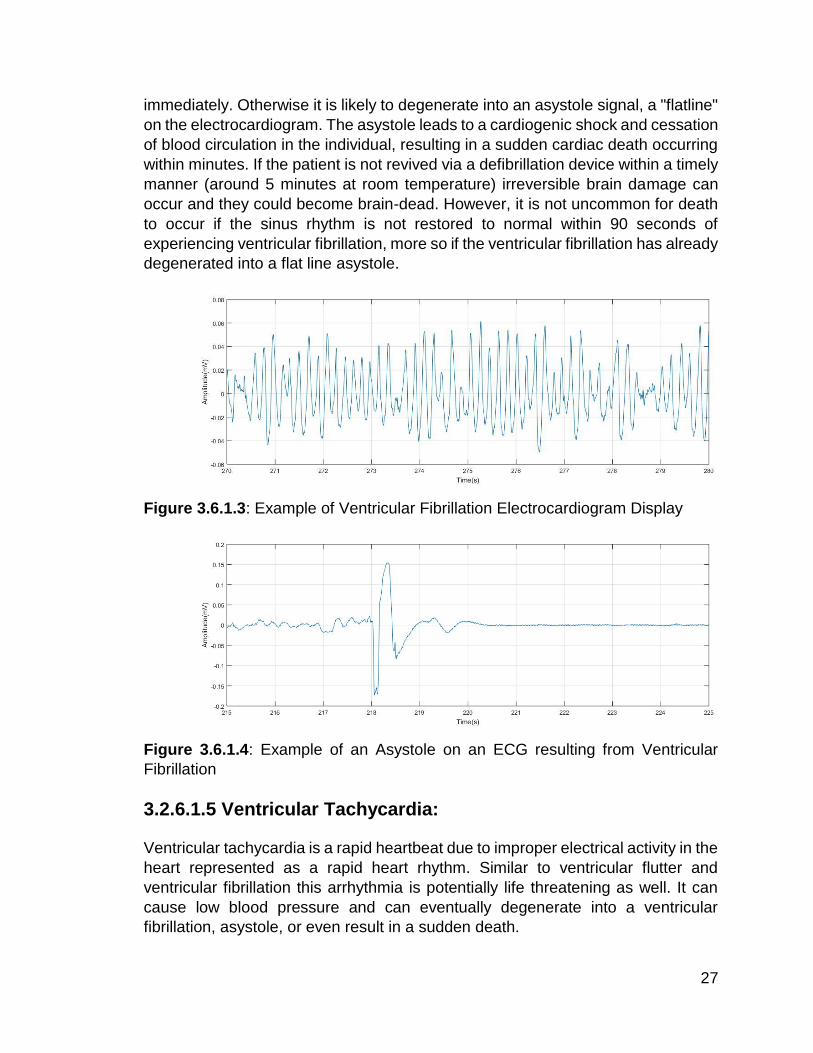
27
immediately. Otherwise it is likely to degenerate into an asystole signal, a "flatline"
on the electrocardiogram. The asystole leads to a cardiogenic shock and cessation
of blood circulation in the individual, resulting in a sudden cardiac death occurring
within minutes. If the patient is not revived via a defibrillation device within a timely
manner (around 5 minutes at room temperature) irreversible brain damage can
occur and they could become brain-dead. However, it is not uncommon for death
to occur if the sinus rhythm is not restored to normal within 90 seconds of
experiencing ventricular fibrillation, more so if the ventricular fibrillation has already
degenerated into a flat line asystole.
Figure 3.6.1.3: Example of Ventricular Fibrillation Electrocardiogram Display
Figure 3.6.1.4: Example of an Asystole on an ECG resulting from Ventricular
Fibrillation
3.2.6.1.5 Ventricular Tachycardia:
Ventricular tachycardia is a rapid heartbeat due to improper electrical activity in the
heart represented as a rapid heart rhythm. Similar to ventricular flutter and
ventricular fibrillation this arrhythmia is potentially life threatening as well. It can
cause low blood pressure and can eventually degenerate into a ventricular
fibrillation, asystole, or even result in a sudden death.
28
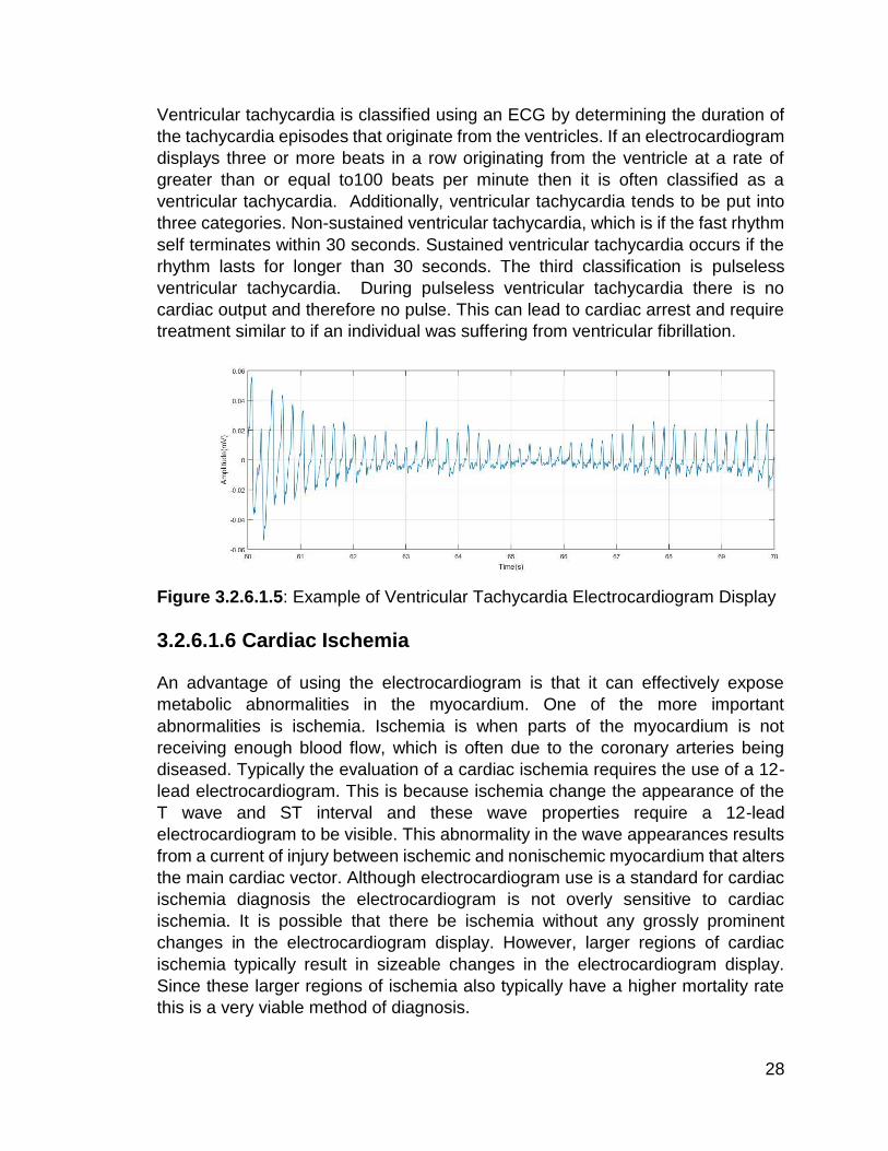
Ventricular tachycardia is classified using an ECG by determining the duration of
the tachycardia episodes that originate from the ventricles. If an electrocardiogram
displays three or more beats in a row originating from the ventricle at a rate of
greater than or equal to100 beats per minute then it is often classified as a
ventricular tachycardia. Additionally, ventricular tachycardia tends to be put into
three categories. Non-sustained ventricular tachycardia, which is if the fast rhythm
self terminates within 30 seconds. Sustained ventricular tachycardia occurs if the
rhythm lasts for longer than 30 seconds. The third classification is pulseless
ventricular tachycardia. During pulseless ventricular tachycardia there is no
cardiac output and therefore no pulse. This can lead to cardiac arrest and require
treatment similar to if an individual was suffering from ventricular fibrillation.
Figure 3.2.6.1.5: Example of Ventricular Tachycardia Electrocardiogram Display
3.2.6.1.6 Cardiac Ischemia
An advantage of using the electrocardiogram is that it can effectively expose
metabolic abnormalities in the myocardium. One of the more important
abnormalities is ischemia. Ischemia is when parts of the myocardium is not
receiving enough blood flow, which is often due to the coronary arteries being
diseased. Typically the evaluation of a cardiac ischemia requires the use of a 12-
lead electrocardiogram. This is because ischemia change the appearance of the
T wave and ST interval and these wave properties require a 12-lead
electrocardiogram to be visible. This abnormality in the wave appearances results
from a current of injury between ischemic and nonischemic myocardium that alters
the main cardiac vector. Although electrocardiogram use is a standard for cardiac
ischemia diagnosis the electrocardiogram is not overly sensitive to cardiac
ischemia. It is possible that there be ischemia without any grossly prominent
changes in the electrocardiogram display. However, larger regions of cardiac
ischemia typically result in sizeable changes in the electrocardiogram display.
Since these larger regions of ischemia also typically have a higher mortality rate
this is a very viable method of diagnosis.
29
3.3 Sampling and Quantization Theory
The main focus of the wireless wearable electrocardiogram is to acquire and
accurately display the wearer's electrical activity of their heart. This signal is
typically an analog signal, continuous time and continuous amplitude. In order to
be wirelessly transmitted and processed the signal must be converted to a digital
signal, which is a discrete time discrete amplitude signal. In order to go from one
type of signal to the other the signals must first be sampled and then quantized.
There are two methods of sampling. Sampling in the time domain and sampling in
the frequency domain. For the purpose of this project we are sampling the analog
electrocardiogram signal in time and therefore will mainly discuss the effects of
sampling in time.
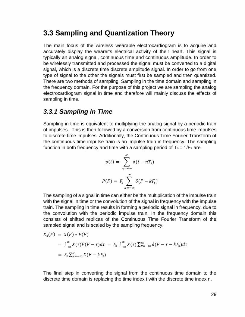
3.3.1 Sampling in Time
Sampling in time is equivalent to multiplying the analog signal by a periodic train
of impulses. This is then followed by a conversion from continuous time impulses
to discrete time impulses. Additionally, the Continuous Time Fourier Transform of
the continuous time impulse train is an impulse train in frequency. The sampling
function in both frequency and time with a sampling period of Ts = 1/Fs are
𝑝(𝑡) = ∑ 𝛿(𝑡 − 𝑛𝑇𝑠)
∞
𝑛=−∞
𝑃(𝐹) = 𝐹𝑠 ∑ 𝛿(𝐹 − 𝑘𝐹𝑠)
∞
𝑘=−∞
The sampling of a signal in time can either be the multiplication of the impulse train
with the signal in time or the convolution of the signal in frequency with the impulse
train. The sampling in time results in forming a periodic signal in frequency, due to
the convolution with the periodic impulse train. In the frequency domain this
consists of shifted replicas of the Continuous Time Fourier Transform of the
sampled signal and is scaled by the sampling frequency.
𝑋𝑠(𝐹) = 𝑋(𝐹) ∗ 𝑃(𝐹)
= ∫ 𝑋(𝜏)𝑃(𝐹 − 𝜏)𝑑𝜏 = 𝐹𝑠 ∫ 𝑋(𝜏) ∑ 𝛿(𝐹 − 𝜏 − 𝑘𝐹𝑠)𝑑𝜏∞𝑘=−∞
∞
−∞
∞
−∞
= 𝐹𝑠 ∑ 𝑋(𝐹 − 𝑘𝐹𝑠)∞𝑘=−∞
The final step in converting the signal from the continuous time domain to the
discrete time domain is replacing the time index t with the discrete time index n.

30
3.3.2 Aliasing
One issue that can arise from sampling is aliasing. Due to the sampling of a signal
in time resulting in a periodic representation of the signal in frequency it is possible
that the signal in the frequency domain overlaps with other samples of that same
frequency. Therefore the sample obtained at a particular frequency could be
misleading and actually represent another frequency than that of the originally
sampled signal. For example, sampling a continuous time sinusoid,
𝑥(𝑡) = 𝑎 𝑐𝑜𝑠(𝜔𝑡 + 𝜑) = 𝑎 𝑐𝑜𝑠(2𝜋𝐹𝑡 + 𝜑)
results in the discrete time sinusoid,
𝑥[𝑛] = 𝑥(𝑛𝑇𝑠) = 𝑎 𝑐𝑜𝑠(2𝜋𝐹𝑛𝑇𝑠 + 𝜑)
But the issue that arises from sampling is that this sinusoid could be obtained from
sampling similar sinusoids such as
𝑥(𝑡) = 𝑎 𝑐𝑜𝑠(2𝜋(𝐹 + 𝑘𝐹𝑠)𝑡 + 𝜑), 𝑘 ≥ −𝐹/𝐹𝑠
Or
𝑥(𝑡) = 𝑎 𝑐𝑜𝑠(2𝜋(𝑙𝐹 − 𝐹𝑠)𝑡 − 𝜑), 𝑙 > 𝐹/𝐹𝑠
This means that once the signal has been sampled it is hard to determine the
frequency of the original continuous time signal because it could be F or F+Fs or
F+2Fs, etc., or with a phase reversal, Fs-F, or 2Fs-F, etc. More generally, aliasing
can be described as a high frequency signal masquerading as a lower frequency
signal. However, an effective method of handling aliasing is to follow the Shannon-
Nyquist sampling criteria and make sure that Fs ≥2F, where F is the largest
frequency in the signal that is being sampled. This guarantees that the sampled
signal can be uniquely recovered after sampling. In addition, high frequency noise
aliasing can be handled by placing an analog antialiasing filter, with a bandwidth
equal to the bandwidth of the desired signal, before the sampler.
3.3.3 Quantization:
The next step involved in converting an analog signal to a digital signal after
sampling is quantization. This is when a quantizer takes in the now discrete time
continuous amplitude signal and produces a signal xQ[n] (where the subscript Q
stands for quantized) that can only take on a finite number of values. A common
quantization method is called rounding and involves setting the output xQ[n] equal
to kQ, where Q is the quantization step size and k is the integer closest to x[n]/Q.
The total number of levels required in quantization tends to be a power of two of
the form 2B, where B is the bits needed for the quantizer. This value can be
determined based on knowing the characteristics required for the quantizer. Such
31
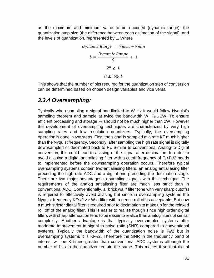
as the maximum and minimum value to be encoded (dynamic range), the
quantization step size (the difference between each estimation of the signal), and
the levels of quantization, represented by L. Where
𝐷𝑦𝑛𝑎𝑚𝑖𝑐 𝑅𝑎𝑛𝑔𝑒 = 𝑉𝑚𝑎𝑥 − 𝑉𝑚𝑖𝑛
𝐿 = 𝐷𝑦𝑛𝑎𝑚𝑖𝑐 𝑅𝑎𝑛𝑔𝑒
𝑄 + 1
2𝐵 ≥ 𝐿
𝐵 ≥ log2 𝐿
This shows that the number of bits required for the quantization step of conversion
can be determined based on chosen design variables and vice versa.
3.3.4 Oversampling:
Typically when sampling a signal bandlimited to W Hz it would follow Nyquist's
sampling theorem and sample at twice the bandwidth W, Fs ≥ 2W. To ensure
efficient processing and storage Fs should not be much higher than 2W. However
the development of oversampling techniques are characterized by very high
sampling rates and low resolution quantizers. Typically, the oversampling
operation is done in two steps. First, the signal is sampled at a rate KF much higher
than the Nyquist frequency. Secondly, after sampling the high rate signal is digitally
downsampled or decimated back to Fs. Similar to conventional Analog-to-Digital
conversion, this could lead to aliasing of the signal after decimation. In order to
avoid aliasing a digital anti-aliasing filter with a cutoff frequency of Fc<Fs/2 needs
to implemented before the downsampling operation occurs. Therefore typical
oversampling systems contain two antialiasing filters, an analog antialiasing filter
preceding the high rate ADC and a digital one preceding the decimation stage.
There are two major advantages to sampling signals with this technique. The
requirements of the analog antialiasing filter are much less strict than in
conventional ADC. Conventionally, a "brick wall" filter (one with very sharp cutoffs)
is required to effectively avoid aliasing but since in oversampling systems the
Nyquist frequency KFs/2 >> W a filter with a gentle roll off is acceptable. But now
a much stricter digital filter is required prior to decimation to make up for the relaxed
roll off of the analog filter. This is easier to realize though since high order digital
filters with sharp attenuation tend to be easier to realize than analog filters of similar
complexity. Another advantage is that typically oversampled systems offer
moderate improvement in signal to noise ratio (SNR) compared to conventional
systems. Typically the bandwidth of the quantization noise is Fs/2 but in
oversampling systems it is KFs/2. Therefore the SNR in the frequency band of
interest will be K times greater than conventional ADC systems although the
number of bits in the quantizer remain the same. This makes it so that digital

32
antialiasing filter removes the additional quantization noise that lies above Fs/2.
However, this is not practical for all applications unless the resolution of the ADC
is reduced and the quantization noise is moved to frequencies above the region of
interest.
3.3.5 Noise Shaping:
The technique used to move the quantization noise to frequencies above the
region of interest is called noise shaping and the most popular technique for noise
shaping is sigma-delta modulation. This technique involves analog-to-digital
conversion of the integral (sigma) of the difference (delta) between the original
signal and the quantized signal. The ADC in sigma delta modulation typically has
a very low resolution but high sampling rate. By averaging over many samples the
digital antialiasing filter that follows the sigma-delta converter is able to reconstruct
the input signal. The sigma-delta modulator can be approximated by the equation
𝑦(𝑡) = ∫ (𝑥(𝜏) − 𝑦(𝜏))𝑑𝜏 + 𝑞(𝑡)𝑡
0
Where x(t) represents the input signal, y(t) the output signal, and q(t) the
quantization noise. Additionally in the frequency domain,
𝑌(𝐹) = 𝑋(𝐹)
1 + 𝑗2𝜋𝐹+
𝑗2𝜋𝐹𝑄(𝐹)
1 + 𝑗2𝜋𝐹
Based on these equations it is apparent that the output is the sum of a term due to
the signal and a term that represents the quantization noise. Furthermore, at low
frequencies the signal term approaches X(F) while the quantization noise term
approaches 0. In contrast, at high frequencies the signal term approaches zero
and the noise term approaches the quantization noise. Therefore, it can be seen
that the sigma delta modulator acts as a lowpass filter for the signal and a highpass
filter for the quantization noise. This is beneficial because it effectively moves the
majority of the quantization noise outside of the frequency band of interest and can
then be filtered afterwards to yield a high SNR.
3.4 Wireless Communications
The following sections discuss the various factors that went into choosing the
wireless communication device as well as the implementation and settings.
3.4.1 Transmission Standard Comparison
For the implementation of wireless transmissions in our project, the decision
between Bluetooth, Wi-Fi and ZigBee chips was a difficult decision when

33
comparing all of the parts. After deciding on the possible chipsets we would use
for each standard, we decided to go with Bluetooth for the multiple reasons. Among
the many requirements that the project contains, meeting both the size and
requirements are at the top of the priority list. Due the limited size of our battery,
the need for an effective low energy transmitter was a main priority. Though the
802.11 chipset does contain the fastest data rate, the battery life compared to the
Bluetooth and ZigBee modules did not meet with our design constraints. ZigBee
although having better battery life than both Bluetooth LE and low power Wi-Fi,
does not have the ability to transmit the same amount of data that may be
necessary within the project. So after comparing the overall constraints involved
with selecting wireless data transmission options, Bluetooth LE was selected since
it gave the best overall balance between, size, price, battery life and data rate.
Below is a chart showing a basic comparison of wireless data transmission
products.
Data Rate Minimum total time to send data (Battery)
Frequencies Range Nodes
Wi-Fi 802.11 (CC3200)
6933Mbps RX: 59 mA TX: 229 mA
5Ghz 500m 8 as router
Bluetooth LE (CC2540)
1Mbps RX: 17.9 mA TX: 18.2 mA
2.4Ghz Up to 10m Up to 8
ZigBee 802.15.1 (CC2630)
250kbps RX: 5.9 mA TX: 6.1 mA
900Mhz 10-100m Up to 65000
3.4.2 Bluetooth LE 4.0 Overview
Among the many options for wireless data transmission we considered the various
platforms that could be used to transmit the data. After these considerations we
decided that Bluetooth would be the best option for us since it provided not only
the best battery life options but also the easiest way to transmit data from UART.
Bluetooth also allowed us to interface easily with mobile devices. Though there are
other Bluetooth modules that provide better transfer rates, ranges and other
benefits. For the purpose of this project Bluetooth LE fulfills our requirements the
best.
3.4.3 Local Bluetooth LE Network
Bluetooth uses a master/slave network model where the master mode of the
Bluetooth sets it’s as the master that broadcasts a communications to a single or
34
multiple slave(s) and can send and request data from the slaves and the slave
mode for can only send and receive data from the master. For our project the hub
that processes and translate the data that will be displayed will have both a master
and a slave chip and two other modules on each electrode.
3.4.3.1 Master/Slave Interfacing and Overview
The CC2541 is a dual mode chip which allows it to be set to both the slave and the
master programmatically. By having this as an option it provides the project much
more flexibility while developing.
3.4.3.2 Data Transfer Rate
The CC2541 supports multiple data rate which range from 250kbps to 2Mbps
these transfer rates give us more than enough speed to move the processed data
from the device to devices throughout the system. Because the CC2541 is used
throughout the project and on each platform there will be no large changes
regarding the data rate from platform to platform. The only place where
bottlenecking could occur is due to an older Bluetooth standard being used in the
Android device.
3.4.3.3 Power Consumption
This module that we selected consumes 14.7ma/14.3ma to 17.9ma/18.2ma of
current depending on whether it is a slave or a master respectively for the RX and
TX in standby and active mode. However for the purpose of the project the RX and
TX will be constantly in active mode as they have to transmit data whenever
possible.
3.4.3.3.1 Wrist Mounted Sensor Consumption
For each wrist mounted sensor, the power consumption will be initially set on active
receive in order to wait for the transmission which states that the consumption for
the device will initially be around 15ma. After it receives the initial signal for the
timer synchronization, the processor then switches the data to transmit to output
the data to the hub.
3.4.3.3.2 Hub Consumption
Because the hub has both a slave and a master, it will be sending a transmission
on its initial start and then set to receive while in the master state in order to meet
all of the initial synchronization settings. Once that message has been sent and is
receiving data from the two wrist mounted electrodes the master module will solely

35
be receiving data until the devices are all turned off. So the master Bluetooth LE
module
For the slave section of the hub it will be also be in active mode the while the device
is on and will only begin transmitting data once it is available in post processing.
3.4.3.3.3 Android Consumption
For the Android connection power consumption there is no set power that can
estimated regarding the Android devices battery life due to the varying chipsets
being used across multiple devices as well as various forms of Bluetooth
implemented across platforms.
3.4.3 Processing
For the data transfer within the system, the current implementation uses
Asynchronous connectionless MAC data transfer. This connectionless system
allows for fast constant data transmission between both the master and the slave
at a rate of about 3ms between transmissions. Because data is constantly
streamed between the two connections, possibly losing a few packets will not
affect the end results since the errors can be filtered out via software when
displaying the data to the user.
3.4.4 Bluetooth Module Settings
This section details the various settings that each Bluetooth module can have
and how they were implemented within the project.
3.4.4.1 Synchronization settings
For our model each electrode’s slave will have a password and unique identifier
for the master module located in the receiver. The Bluetooth modules will be pre-
synchronized with the master in order to skip the inquiry step when activating a
module for the first time. The main reason for limiting user access for the electrodes
is for security and timing situations within the modules.
When connecting to the android device however, it is necessary for the phones
master to inquire and input the proper password before data transmission between
the hub and the Android operating system.
36
3.4.4.2 Connection
For the connection within the processor each device will be set to a standard 9600
baud rate since it allows us enough of a transmission rate throughout the device
for an easy to read accurate signal.
3.4.4.2.1 Wrist Mounted Sensor
The profile for all Bluetooth settings within the wrist mounted slave sensors is going
to be set to active mode. Because the chipsets are all already low energy modules
and the devices will be presynchronized with the module from a Bluetooth LE
transmission point of view, there is no need to limit the transmission between
devices in sniff mode for the wrist sensors.
3.5 Biomedical Signal Processing
Biomedical signal processing is a very broad term. It can refer to genes and protein
sequences, to neural and cardiac rhythms, to even tissue and organ images. Its
main purpose is to extract important information from the broad spectrum of
biomedical signals. This is done via a variety of signal processing techniques, such
as analog signal processing, digital signal processing, and/or statistical signal
processing. The Wireless Wearable Electrocardiogram aims at using signal
processing to provide the user with an accurate representation of their cardiac
rhythm and extracting information from this rhythm to help determine the user’s
heart rate and warn of possible severe arrhythmias.
3.5.1 Biomedical Signal Processing Applications
The human body is constantly communicating information about its health. This is
apparent when someone experiences a fever, cold, or even a muscular ache or
pain. Typically, this information is gathered via medical instruments that take in a
variety of vitals such as a person's blood glucose levels, heart rate, or blood
pressure. Additionally, these vitals are traditionally measured at specific points in
time and recorded on a patient's chart for future reference. This means that if a
patient is to return for additional treatment their diagnosis will most likely be made
based on the combination of their current and past visits vital recordings. To make
matters worse, physicians typically only see less than one percent of these vitals
as they make their rounds to see all their patients. Therefore, medical diagnoses
are based off of prior experience and a much smaller data set than one would
prefer. Biomedical signal processing allows for the analysis and measurement of
typical biomedical vital signals and determine useful information from them. The
more information a physician has to base their diagnoses off of the better. This

37
does a great job of eliminating the trial and error fashion that most diagnosis and
treatments are prescribed.
One application of biomedical signal processing is that it provides the ability to
have real-time monitoring of patients vitals for physicians. This could lead to better
and more accurate diagnoses for patients, or earlier detection of adverse
conditions such as heart attacks. The ability for real time monitoring is especially
useful in critical care settings where any change in a patient's vitals could mean
life or death. Additionally, biomedical signal processing is key to furthering the
understanding of the human body. The human body is a multi-input multi-output
system working together in a closed loop fashion to preserve life. Everything
affects something else. By performing complex analyses on the way the body
reacts to different stimuli we could improve our fundamental understanding of the
body. This could lead to developing techniques for detecting early indicators of
degenerative diseases or just how neurons in the brain interact with one another.
Biomedical signal processing really encompasses all of health and wellness and
its impact will only increase as wearables or other biomedical sensors become
more mainstream. The Wireless Wearable Electrocardiogram will continue this
trend by providing a wearable device for real-time monitoring of the user's heart
activity as well as provide early detection of arrhythmias.
3.6 Electrodes
There are multiple types of electrodes that are used to obtain biopotential signals
from the human body. Some examples are wet electrodes, dry electrodes, and
capacitive electrodes. Additionally, electrodes can vary depending on if they are
used invasively or noninvasively. For electrocardiograms the most common
electrodes are wet non-invasive silver silver-chloride electrodes. In addition to the
silver metal and silver salt of the metal that the electrode is composed of, there
often is some form of electrode paste/jelly that is applied between the electrode
and skin contact. The combination of the paste and silver metal forms a solution
of the metal in the paste at the electrode-skin contact that produces Ag+ ions.
These ions are key for detecting the electric field in the body. When the electric
field set up by the dissolving Ag+ ions is balanced by the forces of the concentration
gradient ionic equilibrium will take place. This causes a monomolecular layer of
Ag+ ions to develop at the surface of the electrode along with Cl- ions. This
combination is referred to as the electrode double layer and is where the half-cell
potential occurs. This half-cell potential is around .8V in the silver silver-chloride
electrodes. The typical equivalent circuit for an electrode consists of resistive and
capacitive components. The capacitor represents the double layer of charges
separated by the dielectric and the resistance is represented by the non-
polarizable behavior of the silver silver-chloride electrodes. However, to accurately
account for the fact that impedance does not increase to infinity as the frequency

38
goes towards zero, a parallel resistance needs to be added. This resistor
represents the electrode-electrolyte interface. The electrode-electrolyte interface
plays a key role in movement artifact noise. If an electrode is moved with respect
to the electrolyte, it can change the distribution of charge at the contact and causes
a change in the half-cell potential until equilibrium is re-established. Now if a pair
of electrodes are in contact with an electrolyte and one moves while the other does
not, it can lead to a potential difference between the two electrodes. And this
potential, the movement artifact noise, is a serious cause of interference ECG
measurement and instrumentation.
Figure 3.6- Silver Silver-Chloride Electrode (Ag-AgCl) Equivalent Circuit
3.7 Signal Conditioning
The electrocardiogram signal is a very low frequency and low amplitude signal.
Typically low frequency and high frequency noise is a much higher amplitude than
the desired biopotential signal. In order to accurately display and process a sinus
rhythm the signal must be carefully conditioned prior to digitization, transmission,
and instrumentation. Conditioning the signal consists of multiple stages of filtering,
buffering, and amplification.
3.7.1 Noise Sources:
The main sources of noise that interfere with acquiring accurate electrocardiogram
readings are very low frequency motion artifact noise, main/power line
noise(60Hz), and common mode noise. If any of these signals are not properly
filtered out or conditioned the acquired signal from the electrode will be inaccurate
and be overtaken by the noise. Motion artifact noises are the signals in the range
0-.5 Hz and tend to come from movement, loose contact of the electrode to the
patient, or due to respiration, which causes a baseline drift of the signal.
Additionally, power line noise has the same effect on the electrocardiogram signal
but at 60Hz. Furthermore, since the typical bandwidth of interest for a diagnostic
ECG is from.5-100 Hz any frequency above that can be considered noise that

39
would negatively impact the desired signal. Lastly, a large source of interference
is the common mode noise that manifests itself across both terminals of the
differential amplifier that is the result of impedance mismatch of the electrode
contacts. Due to the mismatch some of the common mode voltage could be
mistakenly be converted into differential voltage and displayed in the final output
signal.
3.7.1 Filtering/Noise Reduction:
There are multiple methods of noise reduction for these sources of noise that aid
in conditioning the desired signal. First of all, a highpass filter with a cutoff
frequency of .5Hz will eliminate the motion artifact noise and an analog lowpass
filter with a cutoff frequency of 100 Hz will serve as an antialiasing filter as well as
eliminate high frequency noise. Additionally, the high pass filter can be
implemented either via analog circuitry before sampling or digitally in post
processing after conversion. The use of analog filters allows for the directly
acquired signal to be much cleaner than the signal would be without high pass
filtering. However, by implementing the filtering digitally it allows for a reduction in
scale of the analog front end of the device. A notch filter of 60Hz will adequately
handle the power line noise and similarly can be implemented via analog or digital
filtering techniques. The most effective method of reducing common mode noise
is by using an instrumentation amplifier with a very high common mode rejection
ratio (CMRR) on the order of 100dB. Another commonly implemented method of
common mode noise reduction is the implementation of the driven right leg circuit.
Which drives the patient's body with an inverted common mode signal and
significantly reduces the common mode noise as well as reduces the strength of
the power line noise present in the system. However, this circuit requires the use
of an additional electrode in addition to the already attached electrodes. One last
method of reducing common mode noise from impedance mismatching is to make
sure to use the same electrodes and wires and ensure the age of the electrodes
and wires match as well.
3.7.2 Amplification:
After the filtering of the noise sources the resultant signal will be a very low
amplitude bio potential signal from the electrode. In order to convert the signal from
analog to digital and then accurately processed it must be amplified. This is done
via a series of gain stages in the circuit design to amplify the signal enough to be
digitized and displayed properly. Alternatively, this step can be done after the
instrumentation amplifier stage of conditioning.

40
3.8 Power Management
A sufficient power source will be needed to power the ECG. Each wristband will
have its own individual rechargeable battery with charging circuitry. The hub will
be powered by an AC/DC adaptor that will plug into a standard US outlet providing
120 volts at 60 Hz and step down and rectify the voltage to 5 volts DC with a max
current output of at least 500 mA.
3.8.1 Rechargeable Battery Technologies
In choosing the right rechargeable battery a comparison between the two leading
types of rechargeable batteries needed to be researched. Studies show that
between lithium ion and nickel cadmium batteries, lithium ion batteries have a
larger energy density than nickel cadmium batteries. Lithium ion batteries also do
not suffer the “memory effect” where nickel cadmium batteries are affected by
repeatedly charging after a partial discharge and may lose their maximum
capacity. The comparison showed that the most suitable battery technology for
powering the wristbands was the lithium ion battery for its superiority in energy
density, size and weight, and lack of memory effect.
3.8.2 Charging Circuitry
For the prototyping phase the ECG will use 3.7 volt lithium ion batteries connected
to an Adafruit USB charging circuit. The charging circuit will be used exclusively
for the prototyping stage and the final product will utilize the same charging chip
(MCP73833) as the Adafruit circuit on the final PCB. 150 mAh li-ion batteries will
be small enough to support the power needs of the circuit while still minimizing
size of the total product.
Through early prototyping the combination of two sensors to acquire an ECG
signal used only 33 mA at an input bias of ± 5 volts for all dual power op amps
combined. Most if not all of the other ICs involved in the WWECG are rated as low
power devices and are not expected to draw more than 100 mA leaving the total
current draw under the 150 mAh capacity of the chosen lithium ion batteries. This
will allow for the wristbands to function up to around 1 hour which is longer than
the intended run time of one use (~20 minutes).
If found that the 150 mAh batteries do not match the power needs in terms of
capacity, a larger capacity battery will be used. The 3.7v 150 mAh lithium ion
battery chosen for prototyping also comes in a 3.7v 500 mAh package albeit
slightly larger. In this scenario space used will be compromised for a longer lasting
charge to power the device.

41
3.8.3 DC-DC Converters
DC to DC converters are widely used in portable electronics, the reason being that
many portable electronics encompass circuits that require a different voltage level
to operate than the battery of the device is outputting. The main electronic methods
for converting DC voltages consist of linear regulation, switched mode conversion,
magnetic conversion, and capacitive charge pump conversion.
3.8.3.1 Linear Regulators
Linear regulators take an input voltage and output a voltage at a lower level. This
is done through power dissipation as the difference in power of the input and output
is released as heat. When working with large input voltages relative to output
voltages linear regulators are not recommended for their inefficiency in power
dissipation. Because of this power loss through heat many linear regulators come
with heatsinks attached to their ICs. The large advantage linear regulators have
over switched mode regulators is their lack of switching noise.
Low dropout regulators (LDO) have become useful in handheld electronics for their
ability to regulate the output voltage when the input voltage is very close in value
to the output voltage thus reducing the waste of power coming from regulators in
high voltage circuits.
One of the integrated circuits used in the WWECG requires a bias voltage between
2.5V and 3.6V. Since the lithium ion battery selected to power the device provides
3.7V an LDO will be used to drop the voltage down to 3.3V to be usable by the IC.
3.8.3.2 Switched Mode Regulators
Switched mode converters use energy storage components like inductors and
capacitors in conjunction with semiconductor devices as switches to temporarily
store energy in electric or magnetic fields. Generally field effect transistors (FETs)
are used for their switching efficiency to open and close the circuit allowing for the
energy to be stored and then released when needed thus increasing (Boost
converters) or decreasing (Buck converters) the output voltage from the input
voltage.
The benefits of using switch mode regulators include their efficiency in terms of
power loss. Where linear regulators are considered inefficient in high voltage
scenarios due to the power dissipation through heat, switched mode regulators are
considered to be more efficient in that there is no loss through heat.
Switching regulators which utilize components such as inductors to store energy
in a magnetic field make up the magnetic conversion portion of DC-DC converters.
The main drawback of switched mode converters that use inductors is the
42
electromagnetic interference caused by the generating and collapsing of magnetic
fields in the inductors and also transient responses at high switching frequencies.
Many of the ICs used in the WWECG require a bias voltage of 5V. As the battery
selected provides 3.7V a boost converter will be used to bump up the voltage from
3.7V to 5V.
3.8.3.2 Capacitive Charge Pumps
Capacitive charge pumps are switching regulators that use capacitors to change
the input voltage into a higher or lower output voltage. Capacitive charge pumps
lack inductors and therefor do produce any electromagnetic interference. Charge
pumps can also be used to invert the input voltage.
The dual supply op amps used in the sensor require a bipolar supply to bias them.
For this reason a charge pump will be used to invert the stepped up 5V from the
boost converter to -5V and will supply the op amp a negative voltage to bias the –
Vcc pin.
3.9 Data Converters
Typically data is transmitted and viewed as either an analog signal (continuous
time, continuous amplitude) or a digital signal (discrete time, discrete amplitude).
Due to the design of the wireless wearable electrocardiogram it will be necessary
to move from both types of signals often. A conversion of analog to digital will be
needed for Bluetooth wireless transmission of the acquired biopotential signals and
to be processed by the digital signal processor. In contrast, the signal that is
received after transmission will need to be converted from a digital signal to an
analog signal to serve as inputs into the instrumentation amplifier and output the
desired ECG signal. Therefore both analog to digital converters (ADC) and digital
to analog converters (DAC) will be used.
3.9.1 A/D Converters
Ideally, an analog-to-digital converter takes in an analog input signal that lies within
a certain range and is able to uniquely represent its continuous amplitude with a
limited number of digital outputs. The theoretical ideal transfer function of an ADC
would simply be a straight line but practically it represents more of a staircase
where the center of each step is in line with the ideal straight line. The ADC
consists mainly of two steps, sampling and quantization. Both of which are
explained more in depth in section 3.3. Sampling consists of measuring the signals
continuous amplitude at discrete intervals in time. And quantization involves
estimating the continuous amplitude and evaluating it within a discrete range of
values. Naturally this estimation introduces a small amount of error often referred

43
to as quantization error. As the number of discrete codes that represent the
sampled signal's amplitude decreases the width of the steps of the practical ADC
transfer function. Approaching the ideal straight line of the ideal ADC transfer
function. The step width of the ADC is normally referred to as the least significant
bit and is used as the reference unit for other quantities in the specification.
Additionally, since it defines the number of divisions of the full analog range it is
referred to as the resolution of the converter. The resolution of the converter is
normally expressed in terms of the number of bits that the output code will result
in.
3.9.1.1 Types of ADCs
Throughout this project there were multiple types of analog-to-digital converters,
throughout this section lists which were implemented and why they were chosen
for the WWECG.
3.9.1.1.1 Flash ADC
A flash analog-to-digital converter has a bank of comparators that samples the
input in parallel and individually outputs for their decoded voltage range. This bank
then feeds into a logic circuit that generates a code for each voltage range. This
converter tends to be very fast, capable of gigahertz sampling rates, but usually
has a small resolution.
3.9.1.1.2 Successive-Approximation ADC
The successive approximation ADC uses a comparator to successively narrow the
range the input voltage could fall between. The converter compares the input
voltage to the output voltage of an internal DAC that might represent the midpoint
of the selected voltage range, at each successive step. After each step in the
approximated output is stored in a successive approximation register until the
desired resolution is reached. This method is very similar to a binary search
algorithm.
3.9.1.1.3 Sigma-Delta ADC
The sigma-delta ADC over samples the input signal by a large factor and filters the
signal band. Then a smaller number of bits than required are converted using a
Flash ADC after the filter. An error from the discrete levels of the Flash ADC is
created as well. Then the converted signal and error signal are fed back and
subtracted from the input to the filter. This creates a negative feedback that has
the effect of noise shaping the error so that it does not appear in the desired

44
signal's bandwidth. Lastly, a digital filter follows the ADC to reduce the sampling
rate, filter unwanted noise, and increases the resolution of the output.
3.9.2 D/A Converters
Similar to an ADC the theoretical ideal transfer function of the digital-to-analog
converter would also be a straight line. However, in practice it is more of a series
of points that fall on the ideal straight line. This is because the DAC represents the
limited number of discrete digital input codes by a similar number of discrete
analog output values. The LSB of a DAC represents the height of a step between
successive analog outputs from the converter. And the resolution of the DAC is the
number of possible output levels the DAC is designed to reproduce. A way to view
the DAC is as a digitally controlled potentiometer whose output is a portion of the
full analog voltage determined by a corresponding digital code. Typically the DAC
will convert the digital codes that represent a certain analog value into a series of
impulses that will then need to be processed by a reconstruction filter. The DAC
results in a piecewise constant or staircase-shaped output which is equivalent to
a zero order hold operation and effectively multiplies the frequency response of
the reconstructed signal by a sync function. This results in low level noise added
to the reconstructed signal at multiple harmonics above the Nyquist frequency.
However, similar to using an anti-aliasing filter with a cutoff frequency of 1/2 of the
Nyquist frequency before ADC, the errant noise can be filtered out by using a low
pass filter acting as a reconstruction filter with cutoff frequency 1/2 the Nyquist
frequency. This is effective for constructing a smooth analog signal from a digital
input. Another effective method of removing the noise is to oversample the signal
and noise shape so that the undesired noise lies much above the desired
bandwidth of the reconstructed signal and can easily be filtered out.
3.9.2.1 Types of DACs:
Throughout this project there were multiple types of digital-to-analog converters,
this section lists which were implemented and why they were chosen for the
WWECG.
3.9.2.1.1 Pulse-Width Modulator
The pulse-width modulator DAC involves using a stable current or voltage that is
switched into a low-pass analog filter with the duration that is determined by a
digital input code.
3.9.2.1.2 Delta-Sigma DAC
The delta-sigma DAC employs the oversampling technique and allows for the DAC
to use a lower resolution internally. This DAC is driven with a pulse-density

45
modulated signal, which is created with the use of a low pass filter, step
nonlinearity, and a negative feedback loop. This will result in a high pass filter
acting on the quantization noise and steering it into the high frequencies that are
of little interest. This noise can then be filtered out later via an analog low pass
filter.
4 Standards and Constraints
The following section gives an overview of the standards and constraints that
occur within the project.
4.1 Government Regulations
Because the WWECG can be classified as a medical device, it was necessary to
review and comply with all government regulations.
4.1.1 HIPAA Medical Data Security and Privacy
When considering the application of HIPAA to our project it solely applies to
“converted entities and business associates” according to the US Department of
Health and Human services. Because this project is a proof of concept and will not
be used for any business purposes as well as it not being a covered entity since
there are no current sponsorships the standard HIPAA requirements for the privacy
and security of user data collected by the devices does not apply to this current
project. This project does also not need to use user data since none of the data
within our testing will come from actually people as that would violate clinical trial
regulations. Further information on this topic and the definition of “Covered Entities
and Business Associates” can be found within “160.102 Applicability”.
4.1.2 Radio Frequency Devices FCC
Because the device uses Bluetooth LE ISM frequency of 2.4 GHz that meets all
regulations set regarding the Federal Communications Commission’s Electronic
Code of Federal Regulations “18.301 Operating Frequencies”.
4.2 Bluetooth LE Hardware Constraints
Though Bluetooth LE has many great benefits and uses there are still limitations
to the technology as described below. Although Bluetooth LE has these constraints
when compared to other technologies it provides the best specifications for this
given project.

46
4.2.1 Range
For the Bluetooth module selected, the HM-11, the current accurate limitation is
50ft due to the antenna the AN058 from Texas Instruments. This transmission will
also be restricted to an open air environment since Bluetooth transmits with a 2.4
Gigahertz frequency which does not allow accurate transmission through walls.
4.2.2 Transmitters needed for each Device
Due to the master-slave format that Bluetooth LE has and the way Android handles
Bluetooth the devices used throughout our project, there is a need for at least one
Bluetooth module on each device for transmission purposes. However the problem
occurs, due to Android being unable to be set to a slave. Because the android
device cannot be set as slave for receiving the data, the central hub device needs
to have a separate Bluetooth LE module for both the wrist mounted sensors as
well as the Android device. With the master module being used for the sensors
due to timing constraints and the slave used for the android device this technology
adds one more sensor.
4.2.3 Latency
Though the latency limitation for the 6ms for Bluetooth LE and the CC2541, the
due to the application we are using we will be using 10 second latency transmission
to the central hub. The reason the latency is increased is due to the benefits in
accuracy received throughout the transmission. However when connecting to the
Android device, the new latency will be increased to 30ms in order to provide an
easier sampling rate for the mobile device.
4.2.4 Data Rate
For the over the air data rate on the on both of the Bluetooth modules, we will be
attempting to achieve a data throughput rate of 50kbps since the physical layer
rate is 1Mbps. The same data rate applies from the central hub to the Android
device.
4.3 Bluetooth Software Security Standards
In order to meet HIPPA compliance requirements each of our Bluetooth modules
will be fitted with a password in order to stop the possibility of malicious activity
using the data transmitted. Bluetooth LE is also encrypted with a 128bit AES

47
Counter Mode CBC-MAC mode. There is also the possibility of application layer
based encryption being used when transmitting to the Android Application with
SSL.
4.4 Testing Constraints
Because the WWECG is a wearable device and features readings that come from
the body via an electrode of the largest constraints when testing is testing and
simulating a person without actually using a person. Even with consent of the
individual as to not violate the Nuremberg code, research on human subjects
without proper certification at the university violates policy.
5 Design Plan
The physical design plans for the WWECG consist of two adjustable wristbands
(made either of an elastic material that stretches to accommodate for wrist size or
a plastic strap with an adjustable clasp) and a central hub used for externally
processing data and sending it to the Android app.
Figure 5.1 below shows the inner and outer sides of the wristband. The inner side
of the wristband contains only the electrode clip to snap onto electrodes that will
sit on the palm side of the user’s wrist or forearm. A lead will connect the electrode
snap from the inner side to the signal conditioning circuit before being converted
to digital data to be transmitted. The outer side of the wristband will also house the
charge management portion of the device including a 3.7 volt lithium ion battery,
charge controller, boost converter, and a split rail converter for dual supply bipolar
op amps used for active analog filtering. A female micro USB port will be located
next to the battery that will be used to lock into the hub for charging and clock
synchronization. A microprocessor and Bluetooth transmitter will also be located
on the outer side of the wristbands. While a significant portion of the electronics
could be transferred to the inner side of the wristbands to further reduce their size,
we find that having only the electrode snap on the inner side will provide the most
comfort for the user.

48
Figure 5.1- Inner and outer sides of the wristbands
Figure 5.2 shows the hub which will externally process the ECG signal and send
it to the Android app. The hub will also act as a charging station and clock
synchronizer through the two male USB ports located in the middle of the hub. To
provide power to the hub a female micro USB port will be integrated into the system
to allow the user to connect to a power source using a micro USB to USB 2.0.
These cables are very common and are convenient as many outlets now provide
USB 2.0 ports for USB charging options.
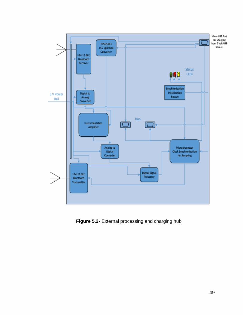
49
Figure 5.2- External processing and charging hub

50
Figure 5.3- Software diagram
5.1 Electrode to Electrode Sampling Synchronization
One of the largest problems that needed to be solved when using designing and
implementing the wrist mounted electrodes for sampling is getting the correct
timing between signals wirelessly transmitted to the receiver. In order to achieve a
proper rhythm strip from the heart, the difference in timing between the electrodes
signals needs to be known before any type of processing can be done on the
signals and outputted through Bluetooth LE to the android device for display.
51
5.1.1 Timestamping
In order to achieve a proper sampling synchronization, it was determined that the
best way to handle the synchronization was to use a timestamp for each device.
Even though the crystal on both chips may be the same, it is impossible to
determine whether or not the actual clock rates on each device will be exactly the
same. Because of this issue the decision was made that timestamping each
transmission was the best way to achieve the most accurate results possible. In
order for each signal to have a timestamp, it is necessary that there is a consistent
time is kept.
5.2.1.1 Timestamp Design Options
In order to decide what was the best option for timestamping each individual device
5.2.1.1.1 CMOS Timestamping
Add a CMOS battery to each modules within the system in order to maintain the
time on each chip with up to 1us of accuracy with a Real Time Clock or RTC
running whenever the device is powered off on each device. So each instance of
the system on initialization will be able to maintain the same time throughout each
device. Only needing to update the current time to the individual microcontrollers
that all have the same time for processing would create a consistent manner of
measuring the difference between electrodes.
5.2.1.1.2 Software Signal Timestamping
Send out a timestamp hosted by the Hub device to send out an original timestamp
with both devices equidistant to the hub and start the timestamp then. This would
occur by placing both wrist mounted electrodes on the hubs Bluetooth masters and
transmitting a start time from both modules at an simultaneous time when ready
with a timestamp. After this timestamp is received by both wrist sensors, they begin
collecting and transmitting data to the back to the hub with the new timestamp that
was calculated from a timer on each board with a simultaneous clock rate along
with the necessary rhythm data. Once the message and timestamp are ready, they
are sent to the hub where the actually rhythm strip will be processed with the new
timestamps from each device then outputted via the Android application.
5.2.1.1.3 Timestamp Implementation
After heavily considering both options, the decision was made to go with the
second decision since it will likely be easier to implement. The first option though
likely simpler to operate would create another layer of complexity from the

52
hardware perspective that would likely cause more harm than good when
implementing the necessary items. The second option however will require a
heavier embedded software implementation but will also allow for reduced size
and weight on each wrist-mounted electrode. The processed is also displayed
below Figure 5.1.1.
Figure 5.1.1 above figure displays the implementation of the devices timestamping
process in order to achieve an accurate synchronization between all individual
sensors.
5.3 Firmware and Software Plan
For the overall programming aspects of design and implementation, Object
Oriented Design will be used. Though the projects embedded software will be
mostly implemented using C, it was determined that Object-Oriented Design

53
aspects would still be best for the implementation of this project since it will help
improve modularity throughout the implementation and debugging steps as well as
allow the software to be more organized and fluid. Below are graphs and briefs
descriptions of the project’s implementations.
5.3.1 Electrode Sensors
This section displays the data flow and the overall class diagrams for the Hubs
embedded software.
5.3.1.1 Data Flow
The data flow diagram below shows how data is collected and then moved
throughout of the system.
Fig 5.3.1.1 below displays the data flow of an electrode node.

54
5.3.1.2 UML Class Diagram
Referencing the diagram in Figure 5.3.1.1 below, one can observe the overall
structure that the embedded software design. Featuring a main thread to move
data between classes this software implementation allows a modular approach to
increase ease of debugging.
Figure 5.3.1.2-Electrode sensor UML Diagram
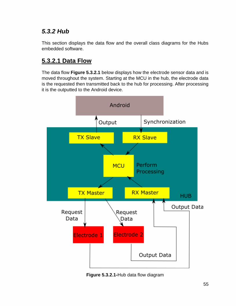
55
5.3.2 Hub
This section displays the data flow and the overall class diagrams for the Hubs
embedded software.
5.3.2.1 Data Flow
The data flow Figure 5.3.2.1 below displays how the electrode sensor data and is
moved throughout the system. Starting at the MCU in the hub, the electrode data
is the requested then transmitted back to the hub for processing. After processing
it is the outputted to the Android device.
Figure 5.3.2.1-Hub data flow diagram
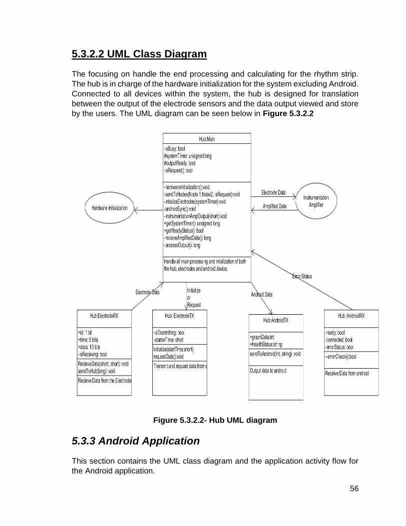
56
5.3.2.2 UML Class Diagram
The focusing on handle the end processing and calculating for the rhythm strip.
The hub is in charge of the hardware initialization for the system excluding Android.
Connected to all devices within the system, the hub is designed for translation
between the output of the electrode sensors and the data output viewed and store
by the users. The UML diagram can be seen below in Figure 5.3.2.2
Figure 5.3.2.2- Hub UML diagram
5.3.3 Android Application
This section contains the UML class diagram and the application activity flow for
the Android application.

57
5.3.3.1 Application Flow
For the application flow chart in Figure 5.4.3.1 below Circles indicate actions, squares indicate a dialog or a screen, arrows indicate flow, dotted lines indicates that you can press back to go to the previous screen.
Figure 5.3.3.1 Application Flow Chart
5.3.3.2 UML Class Diagram
The UML class diagram in the following pagelists the overall design for the Android
application. See client side specification in section 7.3 for further details regarding
the app
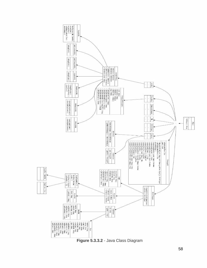
58
Figure 5.3.3.2 - Java Class Diagram

59
5.4 Hub Receiver and External Processing
This section discusses the processing techniques of the hub and the receiver.
5.4.1 Post-Transmission Preprocessing
This stage of the design consists of recreating the Bluetooth LE transmitted signal via Digital-to-Analog converters. We will be using the Texas Instruments DAC8411 16-bit Digital-to-Analog converters due to their low powered nature and high accuracy. Afterwards, the signal will be passed through reconstruction filters similar to the antialiasing filters on the analog front end of the sensors. The -3db frequency of these reconstruction filters will be 100Hz, the same as the antialiasing filters. After successful reconstruction the signals will go through the instrumentation amplifier to remove the common-mode noise seen at the electrode inputs. To complete this task we are using the Texas Instruments INA333 due to its very high Common-Mode Rejection Ratio and low power. This instrumentation amplifier is commonly used in many ECG applications. At this point we will have the desired representation of the Electrocardiogram signal and it will next go through Analog-to-Digital conversion to be passed to the Digital Signal Processor to implement our designed signal processing algorithms. For the Analog-to-Digital conversion we will be using the ADS1251 due to its noise shaping ability since it is a sigma-delta modulating ADC, which reduces quantization error and provides a cleaner signal to the DSP. We are using the TMS320C5535 DSP to implement the algorithms due to its low power nature and the flexibility that software implemented DSPs provide.
5.4.2 Digital Signal Processing Algorithms for ECG signal
Prior to any algorithm implementation it is first necessary to do some preliminary
ECG signal pre-processing and filtering on the digital end. For QRS detection it is
necessary to estimate the energy in the QRS frequency band.
Pre-Processing/Filtering Steps:
1. Filter with a FIR Bandpass filter with pass band of 5-26 Hz.
2. Take the derivative of this bandpass filtered signal.
3. Take the absolute value of the resultant signal.
4. Average the absolute value of the signal over an 80 ms window.

60
5.4.2.1 QRS Complex Detection Algorithm
The QRS complex detection algorithm is based on the popular Pan and Tompkins
algorithm. It consists mainly of a peak detection algorithm. First a threshold is
determined based on the mean estimate of the average QRS peak and the
average noise peak. Additionally, this threshold is automatically adjusted
throughout the algorithm's implementation. The peak will then be classified as
either noise or a QRS complex based on whether it surpasses the detection
threshold or not. There are 4 main rules that the algorithm follows to accurately
differentiate between a QRS detection and a noise peak.
Rule Description
1 Ignore any peak that either precedes or follows a larger peak by less than 196ms.
2 If a peak is detected, then now refer back to the original raw signal and determine if that segment contains both negative and positive slopes. This correlates to a peak being found in the raw signal. Otherwise, the detected peak simply represents a baseline shift.
3 Compare the reported peak to the detection threshold. If larger than the detection threshold the signal is classified as a QRS complex. Otherwise, the signal is classified as noise.
4 Lastly, classify a peak as a QRS complex if no other QRS has been classified within 1.5 R-to-R intervals, but a peak greater than half the detection threshold followed the previous QRS detection by at least 360ms.

61
Figure 5.4.2.1 QRS Block Diagram
62
5.4.2.2 Heart Rate Calculation Algorithm
The algorithm for heart rate calculation is quite simple. It simply counts the number
of QRS complexes occurring over a six second interval and then multiplies that
count by ten. This method requires working in conjunction with the QRS complex
detection algorithm to maintain accuracy.
5.4.2.3 Ventricular Arrhythmia Detection Algorithm
Similar to the QRS complex detection algorithm, the Ventricular Arrhythmia
Detection Algorithm is based on a combination of peak detection and power
spectral density analysis of the ECG signal. However, prior to algorithm
implementation it is important to first extract the specific features we are interested
in. This involved first analyzing normal sinus rhythm signals vs. arrhythmias based
on data provided by MIT's BIH Arrhythmia database. After spectral analysis it was
apparent that the between approximately .5Hz-20Hz arrhythmic behavior
differentiated itself from normal sinus rhythm spectral characteristics. Therefore,
the signal segment was filtered by a digital FIR lowpass filter with cutoff frequency
of 20Hz and a digital highpass filter with a cutoff frequency of .5Hz. This is only for
arrhythmia detection to preserve the desired signal characteristics in this specific
bandwidth. Now after this stage of filtering, analysis was again performed on the
spectrum of the signals and it was determined that there was not any specific
peaks at any specific frequency. However, there tended to be concentrations of
energy in small frequency bands for arrhythmias compared to normal sinus rhythm
signals. This resulted in a sub-band total power approach to detecting the
arrhythmias. For each tested signal segment the power spectral density of each
segment is calculated. Then in sub-bands of 2Hz the total power content in every
2Hz is determined. Afterwards a ratio comparing the power of the tested sub-band
versus the characteristic normal total power is calculated. A peak detection
algorithm is then implemented to determine if any peak ratios in the tested segment
occur above the threshold frequency for arrhythmic activity.
Another component of the detector is a waveform morphology analysis in the time
domain signal. This again employs a peak detection algorithm but this time
determines the length in time between successive peaks. Arrhythmias tend to be
characterized by wider intervals between peaks in their time domain waveforms.
Lastly, a method based on clinically derived QRS complex characteristics of
arrhythmias can be employed in conjunction with the QRS complex detection
algorithm results to accurately detect arrhythmia. Accuracy is key because in a
clinical setting it is important to have as few false alarms and missed alarms as
possible, while still maintaining high accuracy. Therefore, a combination of all
three approaches will most likely result in the most accurate detections. The
detector will be analyzing a new segment of the ECG signal every 5 seconds. The
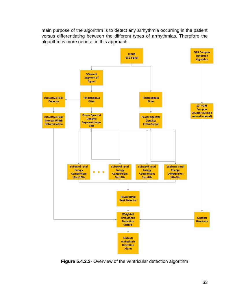
63
main purpose of the algorithm is to detect any arrhythmia occurring in the patient
versus differentiating between the different types of arrhythmias. Therefore the
algorithm is more general in this approach.
Figure 5.4.2.3- Overview of the ventricular detection algorithm
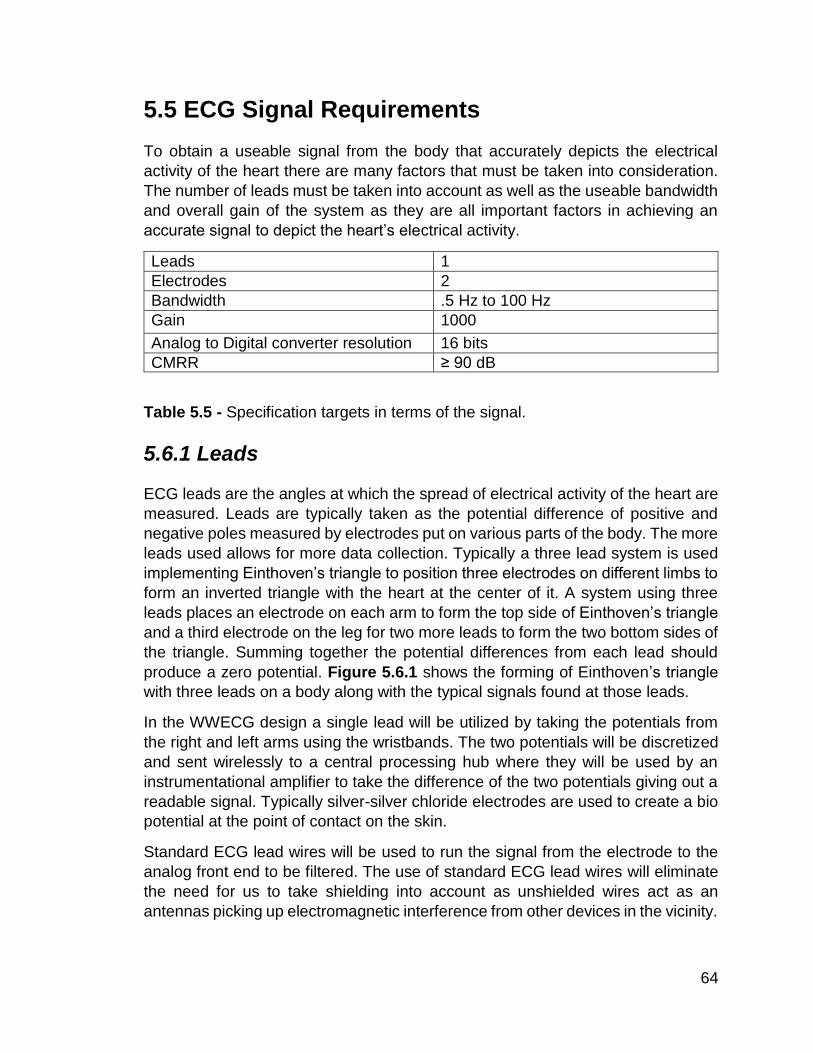
64
5.5 ECG Signal Requirements
To obtain a useable signal from the body that accurately depicts the electrical
activity of the heart there are many factors that must be taken into consideration.
The number of leads must be taken into account as well as the useable bandwidth
and overall gain of the system as they are all important factors in achieving an
accurate signal to depict the heart’s electrical activity.
Leads 1
Electrodes 2
Bandwidth .5 Hz to 100 Hz
Gain 1000
Analog to Digital converter resolution 16 bits
CMRR ≥ 90 dB
Table 5.5 - Specification targets in terms of the signal.
5.6.1 Leads
ECG leads are the angles at which the spread of electrical activity of the heart are
measured. Leads are typically taken as the potential difference of positive and
negative poles measured by electrodes put on various parts of the body. The more
leads used allows for more data collection. Typically a three lead system is used
implementing Einthoven’s triangle to position three electrodes on different limbs to
form an inverted triangle with the heart at the center of it. A system using three
leads places an electrode on each arm to form the top side of Einthoven’s triangle
and a third electrode on the leg for two more leads to form the two bottom sides of
the triangle. Summing together the potential differences from each lead should
produce a zero potential. Figure 5.6.1 shows the forming of Einthoven’s triangle
with three leads on a body along with the typical signals found at those leads.
In the WWECG design a single lead will be utilized by taking the potentials from
the right and left arms using the wristbands. The two potentials will be discretized
and sent wirelessly to a central processing hub where they will be used by an
instrumentational amplifier to take the difference of the two potentials giving out a
readable signal. Typically silver-silver chloride electrodes are used to create a bio
potential at the point of contact on the skin.
Standard ECG lead wires will be used to run the signal from the electrode to the
analog front end to be filtered. The use of standard ECG lead wires will eliminate
the need for us to take shielding into account as unshielded wires act as an
antennas picking up electromagnetic interference from other devices in the vicinity.
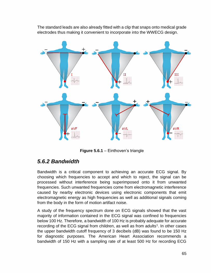
65
The standard leads are also already fitted with a clip that snaps onto medical grade
electrodes thus making it convenient to incorporate into the WWECG design.
Figure 5.6.1 – Einthoven’s triangle
5.6.2 Bandwidth
Bandwidth is a critical component to achieving an accurate ECG signal. By
choosing which frequencies to accept and which to reject, the signal can be
processed without interference being superimposed onto it from unwanted
frequencies. Such unwanted frequencies come from electromagnetic interference
caused by nearby electronic devices using electronic components that emit
electromagnetic energy as high frequencies as well as additional signals coming
from the body in the form of motion artifact noise.
A study of the frequency spectrum done on ECG signals showed that the vast
majority of information contained in the ECG signal was confined to frequencies
below 100 Hz. Therefore, a bandwidth of 100 Hz is probably adequate for accurate
recording of the ECG signal from children, as well as from adults1. In other cases
the upper bandwidth cutoff frequency of 3 decibels (dB) was found to be 150 Hz
for diagnostic purposes. The American Heart Association recommends a
bandwidth of 150 Hz with a sampling rate of at least 500 Hz for recording ECG

66
signals. This recommendation meets the Nyquist Theorem for sampling rate which
states that the sampling rate must be at least twice the highest analog frequency
component. To limit the frequency of the signal to this bandwidth without degrading
the amplitude of it, an active high pass filter must be implemented. The WWECG
will use a combination of second order and single order high pass filters with 3 dB
frequencies of 100 Hz for an attenuation rate of 60 dB per decade. The high
attenuation rate of these filters is beneficial in eliminating unwanted frequencies.
On the lower end of the frequency spectrum factors that introduce electrode
contact noise must also be taken into consideration and filtered out so they do not
skew the accuracy of the signal. Such things as loose contact, motion artifacts,
and baseline drift due to respiration all affect the fidelity of the signal. With the
exception of movement, all these interferences occur around or below .5 Hz. To
limit the frequency of the signal to this bandwidth without degrading the amplitude
of it, an active low pass filter must be implemented. A combination of second order
high pass filters with 3 dB frequencies of .5 Hz for an attenuation rate of 60 dB per
decade will be used.
One specific frequency that falls into the bandwidth requirements for an ECG
signal that can typically cause interference is 60 Hz mains noise generated by local
power lines. Because this interference occurs at a frequency inside the desired
bandwidth it must also be filtered out. To filter out on specific frequency in the
analog domain a notch filter must be implemented. A notch filter is a band reject
filter whose quality factor is very larger allowing for high attenuation around the
specific frequency desired for rejection
5.6.3 Gain
The signals given off by the heart’s electrical activity can be detected by placing
electrodes on the skin however the signal strength from these electrodes is small.
The signal strength in terms of amplitude is normally found to be in the range of 1
to 3 millivolts when display on an ECG device but is found in the microvolts range
when coming from the body. Thus for the signal to be read by digital equipment it
must first be amplified to a level within the detectable range of the equipment. For
the signal to be detected it will need to be amplified from the microvolt range to the
millivolt range thus amplifying it by a thousand. With such a high gain it will be
important to make sure that any noise caused by the electrodes is filtered out
otherwise that noise is also amplified by a gain of one thousand. Given such a high
gain the sensitivity of both the signal and noise is greatly increased meaning a tiny
motion artifact in the original signal could be represented as a much higher error.

67
For this amplification an inverting amplifier will be used with a gain ratio of one
thousand calculated by the transfer function of the amplifier 𝐻(𝑠) =𝑅2
𝑅1 where 𝑅2=
100 kΩ and 𝑅1= 100 Ω. The use of an inverting amplifier allows for a simplified
gain equation and also inverts a negative signal from filtering stages of the
WWECG to a positive signal.
5.6.4 Resolution
Because of the nature of the signal taken from the body, much amplification is
needed for digital equipment to be able to use it. The resolution of the sensor will
depend on the data conversion. The differences between an ECG being
considered standard or high resolution are dependent on a few categories. Of
these categories the WWECG meets only one requirement of a high resolution
ECG having a 16 bit analog to digital converter.
Standard Resolution ECG High Resolution ECG
Low digital signal resolution High signal resolution
ECG signal bandwidth 0 Hz -100 Hz Wider signal bandwidth of .05 Hz – 300 Hz
8 bit Analog to Digital converter 12 bit Analog to Digital converter
Cannot detect late potentials Can detect late potentials
Focused on all portions of the signal Focused on terminal portion of QRS complex and further regions
Key analysis of PR interval, QRS duration, ST segment elevation
Key analysis of QRS duration, RMS40 and LAS40
Table 5.6.4- ECG Resolution Comparison
The desired magnitude of the signal will range between 5V and -5V using a 16 bit
data converter per wristband. To achieve a resolution using 16 bits the quantization
step size must be calculated. The levels of quantization must be greater than 2 to
the power of bits, 2𝑏 ≥ 𝐿 where b is equal to the number of bits and L is the level
of quantization. The level of quantization is represented by the number of steps of
quantization plus one. The number of steps is represented as the maximum
magnitude of the range minus the minimum divided by the quantization step size 𝛥.
Manipulating these equations will end in calculating the quantization step size 𝛥.
𝐿 = 𝑠 + 1 𝑠 =𝑉𝑚𝑎𝑥−𝑉𝑚𝑖𝑛
𝛥 216 ≥
5−(−5)
𝛥+ 1
𝛥 ≥10
216−1 𝛥 ≥ 1.5259𝑒 − 4

68
5.6.5 Common Mode Rejection Ratio
The common mode rejection ratio (CMRR) is measured in decibels (dB) as 20
times the log base 10 of the differential mode gain divided by the common mode
gain20𝑙𝑜𝑔10 (𝐴𝑑
𝐴𝑐𝑚). In terms of signal fidelity it is an important parameter for
determining the attenuation of any noise entering the system. The instrumentation
amplifier chosen for the design of the WWECG is one with a very high CMRR so
that it is efficient in eliminating large offset signals. The target goal is to have a
CMRR of equal to or greater than 90 dB, which is common among integrated circuit
instrumentation amplifiers.
5.7 Signal Acquisition Stage
The signal acquisition stage is the most vital in electrocardiography as the signal
must be acquired with accuracy and precision. If the fidelity of the signal is weak,
important data can be skewed by noise causing inaccurate readings. The biggest
threat to accuracy of a signal is noise. Noise can be caused by a multitude of
reasons stretching from impedance mismatching to unwanted signals
superimposing on top of the signal in the form of electromagnetic interference.
The process for obtaining a strong signal starts at the electrodes and continues
throughout the analog front end. Once a signal is filtered and amplified to a
discernible value it can be further processed by the digital back end after being
digitized into discrete values. The three main stages that the signal must go
through to be considered readable enough for an analog to digital converter to
digitize it are amplification, anti-aliasing, and noise filtering.
It had been found through testing that no discernable difference in signal quality
can be observed whether the anti-aliasing or noise filtering stages come first.
However it is the personal preference of the design team that the amplification
stage comes last in the signal acquisition stage.
5.7.1 Anti-Aliasing
The anti-aliasing stage is used to restrict the bandwidth of the signal to a range of
.5 Hz to 100 Hz. These cutoff frequencies will be the point in the frequency domain
where the signal shall lose its magnitude by 3 dB as the signal is attenuated. The
benefit of using an anti-alias filter to cut the bandwidth of the signal to a certain
span is that while frequencies of wavelengths outside of the bandwidth still exist,
the device will not register them as readable values.
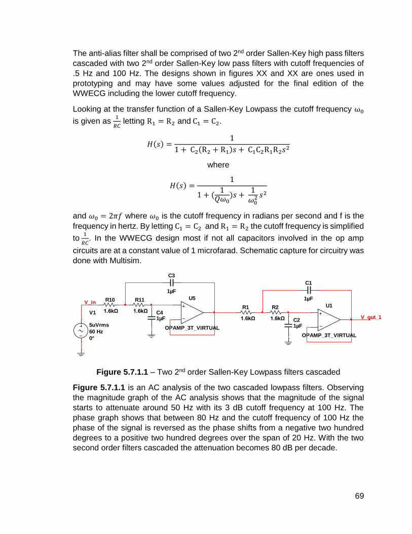
69
The anti-alias filter shall be comprised of two 2nd order Sallen-Key high pass filters
cascaded with two 2nd order Sallen-Key low pass filters with cutoff frequencies of
.5 Hz and 100 Hz. The designs shown in figures XX and XX are ones used in
prototyping and may have some values adjusted for the final edition of the
WWECG including the lower cutoff frequency.
Looking at the transfer function of a Sallen-Key Lowpass the cutoff frequency ω0
is given as 1
𝑅𝐶 letting R1 = R2 and C1 = C2.
𝐻(𝑠) =1
1 + C2(R2 + R1)𝑠 + C1C2R1R2𝑠2
where
𝐻(𝑠) =1
1 + (1
𝑄𝜔0)𝑠 +
1𝜔0
2 𝑠2
and 𝜔0 = 2𝜋𝑓 where 𝜔0 is the cutoff frequency in radians per second and f is the
frequency in hertz. By letting C1 = C2 and R1 = R2 the cutoff frequency is simplified
to 1
𝑅𝐶. In the WWECG design most if not all capacitors involved in the op amp
circuits are at a constant value of 1 microfarad. Schematic capture for circuitry was
done with Multisim.
Figure 5.7.1.1 – Two 2nd order Sallen-Key Lowpass filters cascaded
Figure 5.7.1.1 is an AC analysis of the two cascaded lowpass filters. Observing
the magnitude graph of the AC analysis shows that the magnitude of the signal
starts to attenuate around 50 Hz with its 3 dB cutoff frequency at 100 Hz. The
phase graph shows that between 80 Hz and the cutoff frequency of 100 Hz the
phase of the signal is reversed as the phase shifts from a negative two hundred
degrees to a positive two hundred degrees over the span of 20 Hz. With the two
second order filters cascaded the attenuation becomes 80 dB per decade.
U5
OPAMP_3T_VIRTUAL
C3
1µF
C41µF
R10
1.6kΩ
R11
1.6kΩV1
5uVrms
60 Hz
0°
V_inU1
OPAMP_3T_VIRTUAL
C1
1µF
C21µF
R1
1.6kΩ
R2
1.6kΩ V_out_1
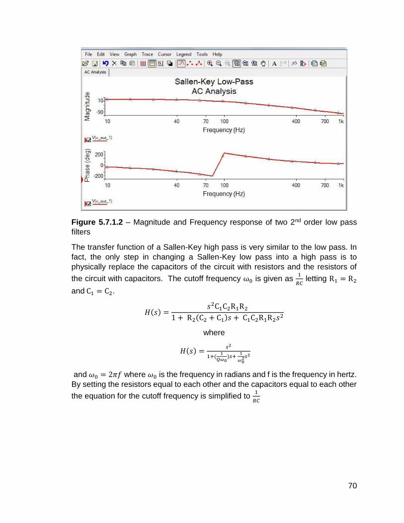
70
Figure 5.7.1.2 – Magnitude and Frequency response of two 2nd order low pass
filters
The transfer function of a Sallen-Key high pass is very similar to the low pass. In
fact, the only step in changing a Sallen-Key low pass into a high pass is to
physically replace the capacitors of the circuit with resistors and the resistors of
the circuit with capacitors. The cutoff frequency ω0 is given as 1
𝑅𝐶 letting R1 = R2
and C1 = C2.
𝐻(𝑠) =𝑠2C1C2R1R2
1 + R2(C2 + C1)𝑠 + C1C2R1R2𝑠2
where
𝐻(𝑠) =𝑠2
1+(1
𝑄𝜔0)𝑠+
1
𝜔02𝑠2
and 𝜔0 = 2𝜋𝑓 where 𝜔0 is the frequency in radians and f is the frequency in hertz.
By setting the resistors equal to each other and the capacitors equal to each other
the equation for the cutoff frequency is simplified to 1
𝑅𝐶

71
Figure 5.7.1.3 – Two 2nd order Sallen-Key Highpass filters cascaded
Figure 5.7.1.4 is the AC analysis in the frequency domain of the two cascaded
highpass filters. Observing the magnitude graph of the AC analysis shows the
attenuation start around 4 Hz and continues to attenuate until it reaches .5 Hz.
There is no signal seen before .5 Hz on neither the magnitude nor phase response
graphs. With the two second order filters cascaded the attenuation becomes 80
dB per decade.
Figure 5.7.1.4 – Magnitude and Frequency response of two 2nd order highpass
filters
5.7.2 Noise Filtering
The greatest source of noise that falls into the useable bandwidth of an ECG is the
mains noise occurring at 60 Hz that comes from local power lines. ECGs use
various techniques to rid the system of this noise including the driven right leg
U6
OPAMP_3T_VIRTUAL
C5
1µF
C6
1µF
R12
318kΩ
R13318kΩ
V1
1uVrms
0.5 Hz
0°
U1
OPAMP_3T_VIRTUAL
C1
1µF
C2
1µF
R1
318kΩ
R2318kΩ

72
circuit and high gain instrumentation amplifiers. While it is possible to create a band
reject filter using a high pass and low pass filter cascaded with each other, it is
more convenient to use a different approach. The Tow-Thomas biquad is a useful
device for this function, instead of having to make high order high pass and low
pass filters with high attenuation rates the Tow-Thomas biquad will allow the
implementation of a notch filter by combining it with a summing amplifier.
Figure 5.7.2.1 – Tow-Thomas Biquad with summing amplifier
Figure 5.7.2.1 shows the Tow-Thomas biquad which has 3 useful outputs located
at V1, V2, and V3. The output at the first op amp V1 has bandpass characteristics,
the output at the second op amp V2 has lowpass characteristics, and the output of
the third op amp V3 acts as an inverting unity gain amplifier.
The cutoff frequency can be determined by 1
𝑅𝐶 when letting all resistors are equal
to each other and all the capacitors are equal to each other. Using 1 microfarad
capacitors and setting the cutoff frequency to 60 Hz the resistor value is found to
be 2.67 kΩ. By using a summing amplifier to sum the input voltage and the output
voltage located the output of the bandpass filter V1 it creates an extremely narrow
stopband or “notch” at 60 Hz thus minimizing any interference from local power
lines. The resistors of the summing amplifier can be chosen arbitrarily so long as
they all match each other in value. 100 kΩ resistors are chosen for convenience
of realistic values.
U1
OPAMP_3T_VIRTUAL
U2
OPAMP_3T_VIRTUAL
U3
OPAMP_3T_VIRTUAL
U4
OPAMP_3T_VIRTUAL
R1
2.67kΩ
C11µF
C2
1µF
R2
2.67kΩ
R3
2.67kΩ R4
2.67kΩ
R5
2.67kΩ
R6
2.67kΩ
R7
100kΩ
R8
100kΩ
R9
100kΩ
V1
1uVpk
100 Hz
0°
V1
V2
V4
V3

73
Figure 5.7.2.2 – AC Analysis of Tow-Thomas Biquad
As seen in Figure 5.7.2.2 the magnitude response of the circuit shows a notch at
60 Hz. The phase response shows a phase shift from a positive two hundred
degrees to a negative two hundred degrees around the cutoff frequency.
Many of the circuits used for the signal acquisition stage have significant phase
shifts. This poses no major concern for this particular application as the sensors
will have the same components built in so whatever phase shift one sensor
experiences will be experiences by the other as well.
5.7.3 Amplification
Because of the nature of the signal the hearts electrical activity is measured in
microvolts, a range that is too small to be used by a digital converter. The signal
must be amplified to a range compatible with an analog to digital converter. A
simple inverting amplifier will accomplish this.
There are two reasons for choosing an inverting amplifier over a non-inverting one,
the first being that before entering the amplification stage the signal is already
inverted due to the combination of anti-aliasing and noise filtering stages so the
amplifier should invert the signal back. The second reason for choosing the
inverting amplifier over the non-inverting is the transfer function. The transfer
function of a non-inverting amplifier is 𝐻(𝑆) =𝑅2
𝑅1+ 1 while the transfer function of
an inverting amplifier is 𝐻(𝑆) =𝑅2
𝑅1. It is much more convenient in terms of
component availability to use an inverting amplifier with a 100 kΩ resistor and a
100 Ω resistor to get a gain of 1000 rather than using the non-inverting amplifier
which would need a 9999 Ω resistor over a 100 Ω resistor to get a gain of at least
1000. Figure 5.7.3.1 shows the schematic for the inverting amplifier.

74
Figure 5.7.3.1 – Inverting Operational amplifier
As shown in Figure 5.7.3.2, it can be observed that the inverting op amp has a
consistent magnitude throughout the bandwidth concerned with for the WWECG.
Figure 5.7.3.2 – AC analysis of Inverting Amplifier
When cascaded together, the overall AC analysis of the signal acquisition stage
can be represented by Figure 5.7.3.2.
Figure 5.7.3.3 – Total AC Analysis of the Sensor
U7
OPAMP_3T_VIRTUAL
R14
100Ω
R15
100kΩVout
V1
1uVrms
0.5 Hz
0°

75
6 Parts and Hardware
The section discusses the specific parts we used to design the hardware and
their key aspects.
6.1 Operational Amplifiers
Two different types of operational amplifiers were used for the filter design. One
op amp was the TL084 quad JFET-Input Op amp. The TL084 has 4 operational
amplifiers built into one integrated chip. The TL084 features high slew rates, low
input bias and offset currents. It comes in both a Dual In-line Package (DIP) as
well as a Small Outline Integrated Circuit (SOIC) package making it a useful
component in using in prototyping as a through hole part as well as the final design
as a surface mount part.
The second operational amplifier used was the LF351, a low cost high speed JFET
input operational amplifier. This device features low noise and offset voltage drift.
6.1.1 Pin Configuration
TL084
Pin Name Pin Description
1 1Out Voltage Output of 1st Op Amp
2 1In- Differential input of 1st Op Amp
3 1In+ Differential input of 1st Op Amp
4 Vcc+ Positive Input Power Supply
5 2In+ Differential input of 2nd Op Amp
6 2In- Differential input of 2nd Op Amp
7 2Out Voltage Output of 2nd Op Amp
8 3Out Voltage Output of 2nd Op Amp
9 3In- Differential input of 3rd Op Amp
10 3In+ Differential input of 3rd Op Amp
11 Vcc- Negative Input Power Supply
12 4In+ Differential input of 4th Op Amp
13 4In- Differential input of 4th Op Amp
14 4Out Voltage Output of 4th Op Amp
LF351
Pin Name Description
1 Balance For tuning the op amp
2 In- Differential input
3 In+ Differential input

76
4 Vcc- Negative Power Supply
5 Balance For tuning the op amp
6 Output Voltage Output
7 Vcc+ Positive Power Supply
8 NC No Connection
6.2 DC-DC Converters
The two DC-DC converters being implemented in the WWECG design are the
LM2663 CMOS charge-pump voltage converter that inverts a positive voltage to
its corresponding negative voltage and the LM2621 low input voltage switching
step up DC-DC converter. Both of these chips are being implemented for biasing
the dual supply op amps with a positive and negative power supply.
6.2.1 Pin Configuration
LM2663
Pin Name Description
1 FC(SD) External Shutdown
2 Cap+ Positive of the Capacitor
3 GND Ground
4 Cap- Negative of the Capacitor
5 Out Output Voltage
6 LV Low voltage operation
7 Osc Oscillation Frequency
8 V+ Positive Power Supply
LM2621
Pin Name Description
1 PGND Power Ground
2 EN Frequency adjust
3 Freq Frequency adjust
4 FB Output Voltage Feedback
5 SGND Signal Ground
6 Vdd Positive Power Supply
7 BOOT Bootstrap Supply for Gate
8 SW Drain of MOSFET switch

77
6.3 Texas Instruments TMS320C5535 DSP
For the wireless wearable ECG we are using a digital signal processor to
implement QRS detection, heart rate detection, and ventricular arrhythmia
detection signal processing algorithms. We have chosen the TMS320C5535 digital
signal processor from Texas Instruments because implementing these algorithms
via software provides much more flexibility in design compared to implementing
via FPGA. Furthermore, the DSP will be housed within the hub/receiver therefore
it is important for flexibility in reprogramming it if necessary. This specific model is
a high performance low power DSP which is ideal for our application since we are
aiming for a portable central hub that will run off of battery. Furthermore its 50-100
MHz cock rate is more than sufficient for this type of application. The peripherals
provided by this digital signal processor were also key in deciding to use this
model. The TMS320C5535 DSP has a Universal Asynchronous
Receiver/Transmitter and Serial Port Interface with four chip selects that will be
used to communicate with the embedded processor after processing so the
processor can then transmit the data via Bluetooth LE to the user's mobile
application. Additionally the TMS320C5535 DSP processor has a tightly coupled
FFT hardware accelerator that will be used for computations in certain
implemented algorithms. Additionally, this digital signal processor was chosen
since it is primarily programmed in C or assembly and uses Texas Instruments'
Code Composer Studio Integrate Development Environment.
6.3.1 Central Processing Unit
The CPU's internal bus is constructed of one program bus, one 32-bit data read
bus, two 16-bit data read buses, two 16-bit data write buses, and additional buses
dedicated to peripherals and Direct Memory Access (DMA) controllers. The
multiple buses present the ability to perform up to four data reads and two data
writes in a single clock cycle. Additionally, each Direct Memory Access controller
has the capability to complete one 32-bit data transfer per cycle, independent and
parallel of the CPU activity. In addition, the TMS320C5535's CPU has two multiply-
accumulate units that are capable of 17-bit x 17-bit multiplication per cycle. It also
sports a 40-bit arithmetic and logic unit that is additionally supported by a 16-bit
arithmetic and logic unit. Lastly, this model allows for the use of a variable byte
width instruction set.
6.3.2 Internal Memory
The TMS320C5535 has On-Chip Dual-Access Ram located in the byte address
range 000000h - 00FFFFh. The DARAM in these addresses are composed of eight
blocks of 4K words each and each block can perform two accesses per cycle.
Furthermore, the DARAM can be accessed by either the internal program, data, or

78
the Direct Memory Access buses. In addition, the TMS320C5535 has a zero-wait-
state ROM as its On-Chip Read-Only Memory. This memory is located at the byte
addresses FE0000h - FFFFFFh and is composed of four 16K-word blocks, that
amounts to 128K bytes of total ROM. The C5535 also has SARAM memory made
up of 32 blocks of 4K words each. The bye address range for this memory is
010000h - 04FFFFh. Each block of SARAM can perform one read or write per
cycle and can be accessed the internal program, data, or Direct Memory Access
buses. Lastly, the TMS320C5535 has 64K bytes of I/O memory for the memory-
mapped registers of its peripherals and system registers. The I/O space is
separate from the program and memory space.
6.4 Instrumentation Amplifier
Once the hub has received the signals from each wrist sensor and they have been
converted from digital signals to analog signals they need to be processed to
produce the desired ECG signal. This processing occurs in the form of a differential
amplifier where the two inputs are the two wrist sensor signals. However, a large
source of noise in the electrocardiogram is the common-mode noise seen at the
input of the body and this can greatly lower the accuracy of the device. Therefore
an instrumentation amplifier with a high common-mode rejection ratio is needed to
maintain accuracy. The INA333 is a viable solution to this problem because of its
common-mode rejection ratio of approximately 100dB.
6.4.1 Texas Instruments INA333
Figure 6.4.1: Configuration of INA333 Instrumentation Amplifier

79
Pin Configuration:
Pin Name Pin Description
1 RG-1 External resistor for the gain of the amplifier connected to amplifier 1.
2 VIN- Differential input tied to amplifier 1.
3 VIN+ Differential input tied to amplifier 2.
4 V- Negative Input Power Supply Voltage
5 Ref Reference pin normally tied to ground.
6 VOUT Voltage output
7 V+ Positive Input Power Supply Voltage
8 RG-2 External resistor for the gain of the amplifier connected to amplifier 2.
6.4.1.1 Gain
The gain of the INA333 is set by an internal resistor RG, which is connected
between pins 1 and 8 of the device. The equation for the gain is
𝐺 = 1 + 100𝑘Ω𝑅𝐺
⁄
6.4.1.2 Noise Performance
The INA333 employs an auto-calibration technique for internal offset correction
and this technique additionally results in reduced low frequency noise. The low
frequency noise typically is around 1µVPP measured from .1Hz to 10Hz at a gain
of 100.
6.4.1.3 Input Bias Current Return Path
The INA333 has a very high input impedance at around 100GΩ. This high input
impedance makes it so that the input bias current changes very little from its typical
value of ±70pA as input voltage varies. Input circuitry must provide a bias return
path for proper operation, otherwise the inputs will float to a potential that exceeds
the common-mode range of the INA33. Additionally, the input amplifiers will
saturate if no bias current return path exists. The bias current return path can be
connected to one input if the differential source input is low. Furthermore, if it is a
high source impedance two equal resistors can be used to provide a balanced
input. This configuration has the advantage of a lower input offset voltage and
better high-frequency common-mode rejection.

80
6.4.1.4 Input Common-Mode Range
The voltage range of the input circuitry for this instrumentation amplifier is
approximately 0.1v below the positive supply voltage and 0.1V above the negative
supply voltage. The linear common-mode input range is related to the output
voltage of the whole instrumentation amplifier. Specifically, the output voltage
swing of the first two differential amplifiers in the instrumentation amplifier limits
the linear input range.
6.5 Bluetooth Module HM-11 with a Texas Instruments CC2541
The current module we selected is an HM-11 which features a Texas Instruments
CC2541 Bluetooth chipset. By using the HM-11 it allows us to easily interface with
the UARTs of the microprocessor for communication between the Bluetooth
modules and their respective master. This the CC2541 allows us to set the state
of each individual model to either a master or slave device. The device features an
active RX down power rate of 17.9 and TX down power rate 18.2. The working
frequency is the standard Bluetooth and Bluetooth LE radio band of 2.4 GHz.
Because the device features the CC2541 it also allows 256kb worth of configurable
space with AT command support which allows the state to be set between being
a master and slave. The device also has a power supply requirement of 3.3V at
50mA.
6.6 Data Converters
This section discusses the data converters used in the hardware.
6.6.1 Analog to Digital Converter
The Wireless Wearable Electrocardiogram's sensors each take in the users
biopotential signal at each limb and transmit the signal via Bluetooth LE to the
receiver/hub. In order to transmit the signal it must first be converted from an
analog signal to a digital signal. Therefore analog-to-digital converters are
employed. We have chosen to use individual ADCs as opposed to the ADCs on
the microcontroller because of advantages this model data converter offers.
6.6.1.1 Texas Instruments ADS1251
The ADS1251 is a 24-Bit 20 kHz, low-power delta-sigma Analog-to-Digital
converter. This ADC operates on a power supply voltage of +5V. This model was

81
primarily chosen due to its sigma-delta modulation data conversion which employs
oversampling and noise shaping to reduce quantization error in conversion.
6.6.1.1.1 Pin Configuration
Pin Name Pin Description
1 +VIN Analog Input: The positive input terminal of the Differential Analog Input
2 -VIN Analog Input: The negative input terminal of the Differential Analog Input
3 +VDD Input: Power Supply Voltage at +5V
4 CLK Digital Input: Device System Clock
5 DOUT/𝐷𝑅𝐷𝑌 Digital Output: Serial Data Output/Data Ready. Indicates when a new output word is available from the ADS1251 Data Output Register. SCLK clocks out the serial data from the serial data output shift register.
6 SCLK Digital Input Serial Clock: The serial clock operates separately from the system clock. Its normal state is LOW but if held at HIGH a modulator reset will occur or it will enter power-down mode.
7 GND Input: Ground
8 VREF Analog Input: Reference Voltage Input
6.6.1.1.2 Analog Input
The ADS1251 uses a fully differential analog input to provide low system noise,
around 98db common-mode rejection and high power-supply rejection. There are
three main items that affect the performance of this data converter. First, the input
impedance can affect the accuracy of the conversion. The input impedance
changes with the system clock frequency of the ADS1251. If the source impedance
is very high it can affect the accuracy by losing a significant portion of the signal
across the external impedance. Secondly, the input or output current needs to be
limited for the ADC. Typically this limit is a maximum of 10mA. Lastly, the
bandwidth of the analog-input needs to be within half of the system clock frequency
to satisfy the Nyquist sampling criteria and avoid signal aliasing. For the purposes
of the Wireless Wearable ECG the signal will be sampled at 250 Hz which is much
less than the system clock frequency of 8MHz.

82
Figure 6.6.6.1.2 Level Shift Circuit for Bipolar Input of ±5V
6.6.1.1.3 Bipolar Input
The bipolar inputs of the ADS1251 need to maintain a voltage between -0.3V and
VDD (Power Supply Voltage). And the reference voltage is normally less than half
of the power supply voltage. Typically one input of the ADS1251 is tied to the
reference voltage, while the other input falls in the range of 0V to 2 ∙ 𝑉𝑅𝑒𝑓 . The
ADS1251 can be configured to accept bipolar inputs tied to ground by using a 3
op amp circuit with a single amplifier with four external resistors.
6.6.1.1.4 Delta-Sigma Modulator
The main reason this model ADC was chosen was for its delta-sigma modulation
functionality. The modulation frequency is equal to taking the system clock's
frequency and dividing it by 6. Therefore, the modulation frequency is equal to
1.333MHz because the system clock frequency is 8MHz. The oversampling ratio
is 64 and is fixed in relation to the modulation frequency. This results in a 20.8 kHz
data rate for a modulation frequency of 1.333MHz and results in decreasing data
output rates for lower system clock frequencies.
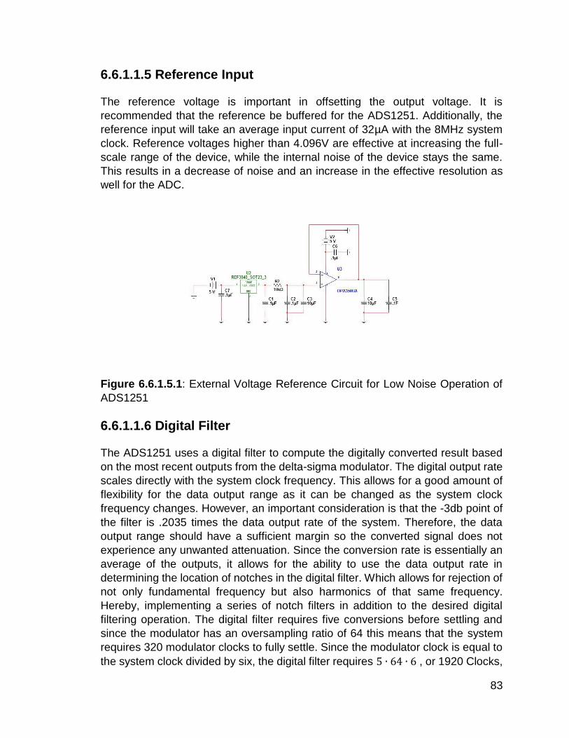
83
6.6.1.1.5 Reference Input
The reference voltage is important in offsetting the output voltage. It is
recommended that the reference be buffered for the ADS1251. Additionally, the
reference input will take an average input current of 32µA with the 8MHz system
clock. Reference voltages higher than 4.096V are effective at increasing the full-
scale range of the device, while the internal noise of the device stays the same.
This results in a decrease of noise and an increase in the effective resolution as
well for the ADC.
Figure 6.6.1.5.1: External Voltage Reference Circuit for Low Noise Operation of
ADS1251
6.6.1.1.6 Digital Filter
The ADS1251 uses a digital filter to compute the digitally converted result based
on the most recent outputs from the delta-sigma modulator. The digital output rate
scales directly with the system clock frequency. This allows for a good amount of
flexibility for the data output range as it can be changed as the system clock
frequency changes. However, an important consideration is that the -3db point of
the filter is .2035 times the data output rate of the system. Therefore, the data
output range should have a sufficient margin so the converted signal does not
experience any unwanted attenuation. Since the conversion rate is essentially an
average of the outputs, it allows for the ability to use the data output rate in
determining the location of notches in the digital filter. Which allows for rejection of
not only fundamental frequency but also harmonics of that same frequency.
Hereby, implementing a series of notch filters in addition to the desired digital
filtering operation. The digital filter requires five conversions before settling and
since the modulator has an oversampling ratio of 64 this means that the system
requires 320 modulator clocks to fully settle. Since the modulator clock is equal to
the system clock divided by six, the digital filter requires 5 ∙ 64 ∙ 6 , or 1920 Clocks,
84
before settling. Therefore, the analog input requires five full conversions to settle
from any significant step change. The transfer function of the digital filter is,
|𝐻(𝑓)| = |sin (
𝜋 ∙ 𝑓 ∙ 64𝑓𝑀𝑂𝐷
)
64 ∙ sin (𝜋 ∙ 𝑓𝑓𝑀𝑂𝐷
)|
5
or in the Z-domain,
𝐻(𝑧) = (1 − 𝑧−64
64 ∙ (1 − 𝑧−1))
5
6.6.1.1.7 DOUT/𝑫𝑹𝑫𝒀
The DOUT/𝐷𝑅𝐷𝑌 output signal alternates between a data ready mode and a data
output mode. The data ready mode indicates that new data has been loaded to the
output register and is ready to be read. Data output mode serially shifts data out
of the Data Output Register. The result of the A/D conversion is written to the Data
Output Register from the Most Significant Bit to the Least Significant Bit.
6.7 Digital to Analog Converter
The receiver/Hub of the Wireless Wearable Electrocardiogram will employ an
instrumentation amplifier to output the analog ECG signal. However, this requires
analog inputs for the differential inputs of the instrumentation amplifier. The wrist
sensors each transmit the biopotential signals via Bluetooth, which means the hub
receives them as digital signals. Therefore, it is necessary to reconvert the digitally
represented signals into the analog domain. Individual Digital-to-Analog converters
were used to achieve this need.
6.7.1 Texas Instruments DAC8411:
The DAC8411 is a 16-Bit low-power, single-channel, voltage output Digital-to-
Analog converter. They provide high quality linearity and reduce unwanted code-
to-code transient voltage. It employs a 3-wire serial interface that operates at clock
rates up to 50MHz and is compatible with SPI and QSPI peripherals. The
DAC8411 uses an external power supply as a reference voltage to set the output
range. Additionally, the DAC8411 uses a power-on reset circuit to make sure that
the DAC output powers up at 0V and stays there until a valid write to the device
occurs. Furthermore, the DAC8411 has a power down feature in which the current
consumption is reduced to 0.1µA at 2V.

85
6.7.1.1 Pin Configuration
Pin Name Pin Description
1 𝑆𝑌𝑁𝐶 Level-triggered control input. Frame synchronization signal for input data. Enables input shift register when low, and data is transferred on falling edge of the following clocks. The DAC8411 is updated following the 24th clock cycle. If HIGH the rising edge acts as an interrupt and the write sequence is ignored.
2 SCLK Serial Clock Input
3 DIN Serial Data Input. Data is clocked into the 24-bit input shift register on the falling edge of the serial clock input.
4 AVDD/VREF Power Supply Input, +2V to +5.5V
5 GND Ground
6 VOUT Analog Output Voltage from DAC.
6.7.1.2 DAC Architecture
The DAC8411 architecture is made up of a string Digital-to-Analog converter (DAC
register followed by Resistor String configuration) followed by an output buffer
amplifier. The power supply acts as a reference for the output due to there not
being a reference input pin on the device. Since the input coding of the DAC8411
is straight binary the ideal output voltage is,
𝑉𝑂𝑈𝑇 = 𝐴𝑉𝐷𝐷 ×𝐷
2𝑛
where n is the resolution size of the data converter, D is the decimal equivalent of
the binary code, and AVDD is the power supply input.
6.7.1.3 Resistor String
The resistor string is exactly what its name implies. A string of resistors at value R
and the code loaded into the DAC register determines at which node of the string
to close the switch and feed the voltage into the output amplifier.

86
Figure 6.7.3.1: Resistor String configuration in DAC8411 Architecture
6.7.1.4 Output Amplifier
The output amplifier buffer can produce rail-to-rail output voltages which allows the
DAC to generate an output range between 0V to the power supply voltage.
6.7.1.5 Power-On Reset to Zero-Scale
The DAC8411 uses a power-on reset circuit to fill the DAC register with zeros on
power up and sets the output voltage to 0. The DAC output register will stay at 0
until a valid write sequence is sent to the DAC.
6.8 Microcontrollers
This section gives a brief overview of the microcontroller used for all data
movement throughout the system.
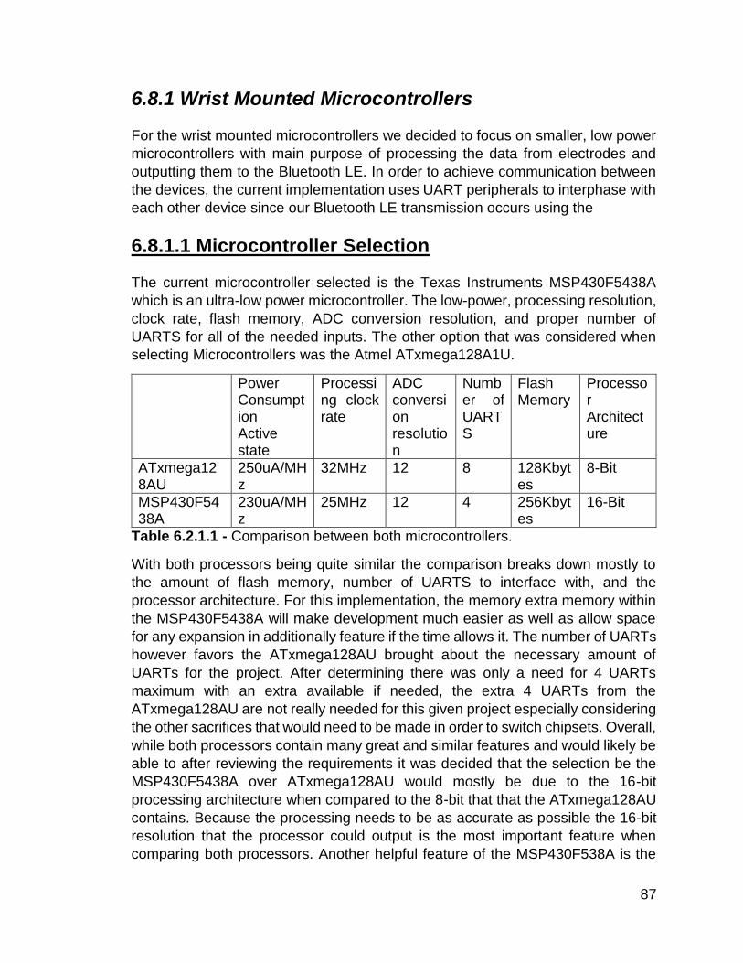
87
6.8.1 Wrist Mounted Microcontrollers
For the wrist mounted microcontrollers we decided to focus on smaller, low power
microcontrollers with main purpose of processing the data from electrodes and
outputting them to the Bluetooth LE. In order to achieve communication between
the devices, the current implementation uses UART peripherals to interphase with
each other device since our Bluetooth LE transmission occurs using the
6.8.1.1 Microcontroller Selection
The current microcontroller selected is the Texas Instruments MSP430F5438A
which is an ultra-low power microcontroller. The low-power, processing resolution,
clock rate, flash memory, ADC conversion resolution, and proper number of
UARTS for all of the needed inputs. The other option that was considered when
selecting Microcontrollers was the Atmel ATxmega128A1U.
Power Consumption Active state
Processing clock rate
ADC conversion resolution
Number of UARTS
Flash Memory
Processor Architecture
ATxmega128AU
250uA/MHz
32MHz 12 8 128Kbytes
8-Bit
MSP430F5438A
230uA/MHz
25MHz 12 4 256Kbytes
16-Bit
Table 6.2.1.1 - Comparison between both microcontrollers.
With both processors being quite similar the comparison breaks down mostly to
the amount of flash memory, number of UARTS to interface with, and the
processor architecture. For this implementation, the memory extra memory within
the MSP430F5438A will make development much easier as well as allow space
for any expansion in additionally feature if the time allows it. The number of UARTs
however favors the ATxmega128AU brought about the necessary amount of
UARTs for the project. After determining there was only a need for 4 UARTs
maximum with an extra available if needed, the extra 4 UARTs from the
ATxmega128AU are not really needed for this given project especially considering
the other sacrifices that would need to be made in order to switch chipsets. Overall,
while both processors contain many great and similar features and would likely be
able to after reviewing the requirements it was decided that the selection be the
MSP430F5438A over ATxmega128AU would mostly be due to the 16-bit
processing architecture when compared to the 8-bit that that the ATxmega128AU
contains. Because the processing needs to be as accurate as possible the 16-bit
resolution that the processor could output is the most important feature when
comparing both processors. Another helpful feature of the MSP430F538A is the

88
ability to debug and program without the need for a JTAG programmer or any other
proprietary cables other than just a USB as opposed to the ATxmega128AU which
needs both a JTAG and aWire for debugging purpose.
6.8.1.2 Power Consumption
One of the main reasons that we chose this microcontroller as opposed to other
options is the overall power consumption. The device features a low supply voltage
range from 3.6 to 1.8V, 230uA/MHz active state consumption, and 3.0V during
flash programmed execution. This consumption rate allows the devices to meet
the hour runtime requirement while also being able to handle of necessary
processing aspects needed for frequency and resolution of the transmission.
6.8.1.3 Peripheral Communications
Featuring four Universal Serial Interface connections or USCI, the
MSP430F5438A also has all of the necessary interface connections to receive,
transmit and accept inputted data throughout the system. Because Universal
Asynchronous Receive/Transmit or UART are simply a type of USCI three of the
ports change be modified to utilize UART in order to handle inputs from the local
ADC and the Bluetooth LE during initialization as well as the constant transmission
to the master of the data that is pulled from the ADC along with the timestamp from
the master.
6.8.1.4 Processing
The MSP430F538A contains a 16-Bit RISC architecture with extend clock memory
of up to 25MHz. The 16-bit input from the analog to digital converter and combine
that with the timestamp. Before transmission, the data will be processed and
shifted down to 12 bits in order to allow the timestamp to be added before being
sent outputted to the Bluetooth LE and sent to the hub.
6.8.1.5 Timers
Because the MSP430F538A also has two timers, a single timer on each
microprocessor will be used for the system clock and will be set at an equivalent
clock rate between both timers via the input clock frequency. With these running
in the background the timestamp variable will be set from that timer.
6.8.2 Central Hub Microcontroller
For the hub microcontroller we chose to focus on a powerful but still efficient device
that could handle both a master and slave node Bluetooth LE peripheral. These

89
Bluetooth LE peripherals would both require receive and transmit pins for each of
the modules. The central hub would also be required to process the data from both
wrist mounted sensors and output this value to the Android device where it can be
displayed. This processing will need to be done quickly a since the inputs from
each wrist mounted sensors will be accepted as fast as possible in order to achieve
the highest resolution which allows for the clearest rhythm strip possible.
6.8.2.1 Microcontroller Selection
For this section the decision was between the Texas Instruments MSP432P401R
and the Atmel AT32UC3L0256. The main deciding factors in determining which
controller to use were low-power, processing resolution, clock rate, flash memory,
ADC conversion resolution, and proper number of UARTS which is similar to the
requirements set for the wrist mounted microcontrollers. The main difference
however is the need for more processing power and being able to sacrifice some
of the previous ultra-low power requirements for this due to larger battery on the
hub. For this project it was determined that the MSP432P401R will be the best
microcontroller for the device.
Power Consumptions active state
Processing clock rate
ADC conversion resolution
Number of UARTS
Flash Memory
Processor Architecture
AT32UC3L0256
110 µA/MHz
50Mhz 12 4 256Kbytes
32-Bit
MSP432P401R
90 µA/MHz 48MHz 12 4 256Kbytes
32-Bit
Table 6.2.2.1 – Microcontroller Comparison
As shown by the graph above, both microcontrollers display very similar overall
specifications. However for this projects purposes it was determined to go with the
MSP432P401R due to its better battery life to processing to clock rate ratio.
Another reason that the MSP432P401R was selected compared to the
AT32UC3L0256 is due to the debugging interface that will be used to program the
board. Because the AT32UC3L0256 uses JTAG and aWire to in order to interface
and the MSP432P401R uses USB with Code Composer Studio, the decision was
made easier due to the familiarity with the debugging interfaces.
6.8.2.2 Power Consumption
Having overall power consumption being a key factor for this microcontroller, with
a supply voltage range of 1.62 to 3.7V and 90 µA/MHz active state consumption.
With these specifications the project should be able to run for up to an hour when

90
processing all of the data. Because the transmission will also be constantly
transmitting via Bluetooth LE to the Android device to display and store data for
the user. The lower processing rate consumption will allow the transmission to
occur much more often providing better results to the user.
6.8.2.3 Peripheral Communications
This microcontroller features four Universal Serial Connection Interface which will
be utilized to send and receive data as well as process the signal and time
differential between the hub and wrist mounted sensors as well as the Android
Bluetooth connection. Because the Android device and the hub itself are both
required to be a master the hub will feature two separate Bluetooth modules
consisting of one slave and one master that will both require two UART pins in
conjunction. The microcontroller also features four more Serial Peripheral
Interfaces which will be used to send and receive data from the digital to analog
converter to be sent through the instrumentation amplifier and resent to the
microcontroller for output.
6.8.2.4 Processing
An overall fairly simple process, the main goal of this microcontroller from a
processing perspective is to keep the proper data in their correct formats the output
the data as fast as possible. Up receiving both signals from the wrist mounted
sensors via a master Bluetooth LE module, the data will then be inputted into the
proper form for the instrumentation amplifier. Once the data is sent through the
instrumentation amplifier it is reprocessed by taking the calculating the difference
from returned timestamps of the original input and the new signal created via the
instrumentation amplifier. This newly processed data will then be outputted to the
second Bluetooth LE slave where it will send the data to the Android device.
7 Software Applications and Database
This section discusses the specifications of the WWECG Server and WWECG
Android application.
7.1 WWECG Server Specifications
This section covers the specifications for all server side activities of the Wireless Wearable ECG. The server side component of the system may be referred to as the WWECG Service or the WWECG Server. The server shall be a LAMP (Linux, Apache, MySQL, and PHP) stack. As seen in figure 7.1, the server is broken up into three main components: the API, the MySQL database, and the file storage.

91
Figure 7.1 - Basic data flow diagram
7.1.1 The Database
The server will use a MySQL database on the server. The database name for this
system shall be “wwecg”.
7.1.1.1 Tables
This section contains the documentation for the database tables and their
respective columns.
7.1.1.1.1 /clients
The /clients table contains all of the client information for the service. For the
prototype we will only be storing our Android app’s credentials here. However if
desired, more than just the official app’s credentials may be stored here.
Column Name Type Description
1 id Integer The id for the client
2 name String The name of the client
3 secret String The secret string for authenticating the client

92
4 is_disabled Boolean Will be true if the client has been disabled by
an admin
A disabled client must not be permitted to
authorize
7.1.1.1.2 /files
The /files table contains records for all files uploaded to the server.
Column Name Type Description
1 id Integer An id for private reference
2 uuid UUID String The public UUID of the file
3 url URL String The URL pointing to the file
4 timestamp Long
Integer
The UNIX timestamp for when the file
was created
5 owner_id UUID String The UUID of the patient that the file
relates to
7.1.1.1.3 /grants
The /grants table contains records that indicate a client’s (and potentially) a user’s
temporary authorization to use the WWECG API and have limited access to the
server.
Column Name Type Description
1 id Integer An id for private reference
2 access_token String The unique string leased to a client for
accessing a user’s account

93
3 refresh_token String
NULLABLE
The unique string to renew the access
token when the token expires
4 user_id UUID
String
The UUID of the user that this
authorization is linked to
5 client_id Integer
NULLABLE
The id of the client this authorization is
linked to
6 expires_at Long
Integer
The UNIX timestamp in which the
access_token is no longer
valid. Typically this should be 3600
seconds after the session is started.
7 is_revoked Boolean Will be false unless the refresh_token
and the access token are both revoked
In the case that a client is disabled, the
authorizations linked to that client
SHOULD be automatically revoked
7.1.1.1.4 /users
The /users table contains records pertaining to user accounts. This includes the
user’s credentials for accessing the app as well as personal information.
Column Name Type Description
1 id Integer An id for private reference
2 uuid UUID
String
A uuid for public reference of this user
3 name_first String The user’s first name
4 name_middle String The user’s middle name
5 name_last String The user’s last name

94
6 password String A KDF hashed password
We will use PBKDF2 with a local salt, a
global salt, and an iteration count of 1024.
This MUST NOT be exposed by the API
and it should only be used to verify user
credentials.
7 salt String The local salt for the password KDF
8 type Enum
String
ADMIN, BANNED, DOCTOR, PATIENT
Doctors, admins, and banned users must
be manually set in the database in the
currently designed system.
9 email String The email address of the user
10 gender Enum
String
The user’s gender
MALE, FEMALE, OTHER
11 birthday Long
Integer
A UNIX timestamp of the user’s birthday
7.1.1.2 Security
This section discusses the security measures used on the database.
7.1.1.2.1 Protected Table Fields
The id fields inside of the database tables MUST NOT to be disclosed via the
API. The users’ PBKDF’d passwords and salts MUST NOT be disclosed by the
API. The client secrets MUST NOT be disclosed by the API.
7.1.1.2.2 Database Access
The database may only be directly accessed by an admin via a direct connection
or by the API. The app must not access the database directly, and only via the
WWECG Service API. Any non HTTPS attempt to the database MUST either be
upgraded to HTTPS or ignored.

95
7.1.1.2.3 Database Sanitization
Any SQL query MUST be sanitized. This is to prevent unauthorized SQL
injections. SQL injections may be trivially be used to read or modify the database
so they must be prevented.
7.1.2 The Application Programming Interface
The API is a collection of PHP endpoints that follow the REST (REpresentative State Transfer) paradigm. All endpoints shall support the HTTPS protocol.
7.1.2.1 Limitations and Constraints
This section discusses the limitations and constraints of the API.
7.1.2.1.1 JSON
JSON (Java Script Object Notation) is a common transport container used with
RESTful interfaces. While it is commonly used, it has some limitations. The
biggest limitation is that it is generally not a streamable data structure, which is ok
for its use in the API, as the API is a RESTful and not a streaming API. Any use
of JSON requires the code to translate the JSON into a Java object. This
constraint is not a tough one to overcome, as one would just have to implement a
JSON decode into their classes to decode the JSON structure.
7.1.2.1.2 REST
REST (REpresentative State Transfer)’s biggest constraint is that it does not allow
for the streaming of data. This means live processing of WWECG session data is
not able to be done on the server side and must be done on the client
side. However, REST will be perfect the post processing of WWECG sessions
that are uploaded to the WWECG Server.
7.1.2.2 Authentication and Security
The API’s authentication model is documented in RFC 6749 As such, the
endpoints MUST use the HTTPS Protocol. Figures 2 and 3 show a complete and
a simplified authentication flow for the API. This implementation of OAuth2
includes the /token “grant_type” parameters of: password, refresh_token, and
client_credentials. This will allow for first party user authentication and client
authentication. The server may use a self-signed or a CA-signed security
certificate.
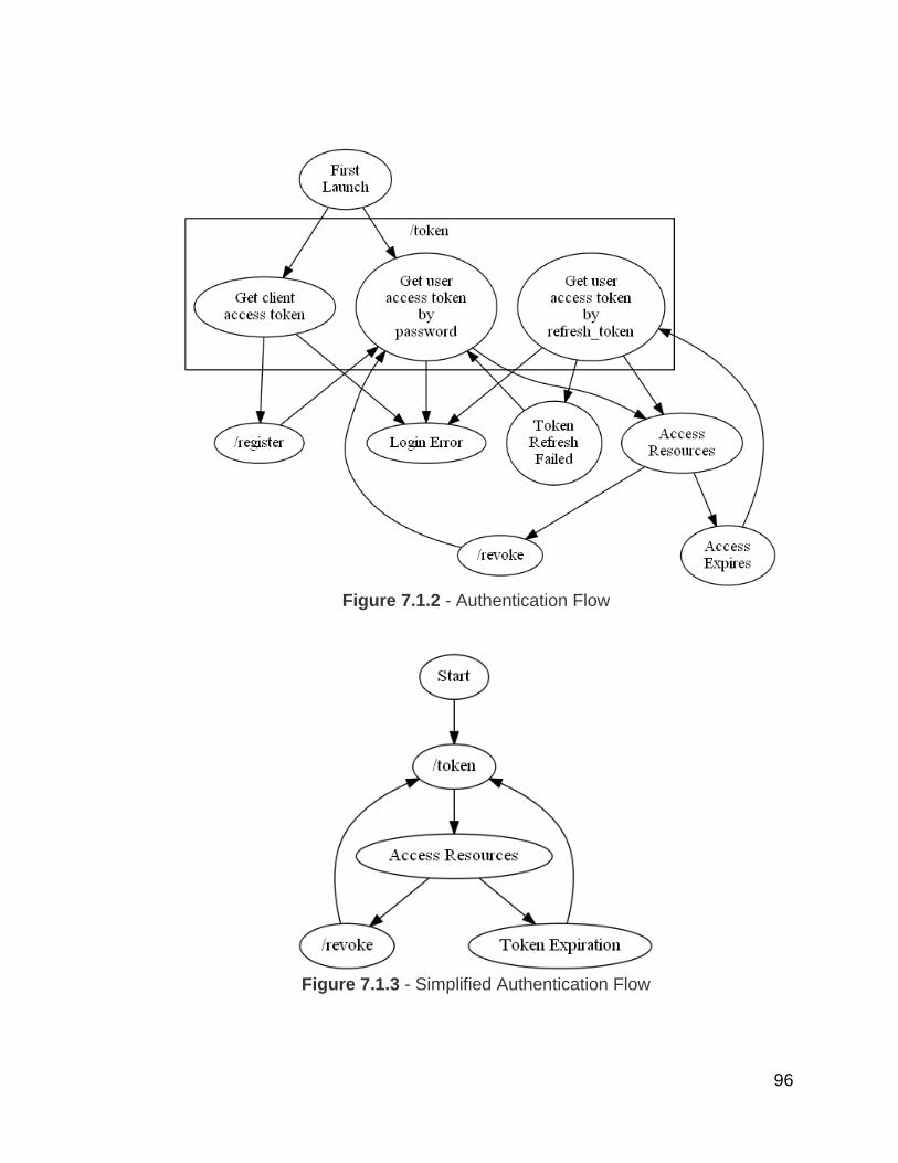
96
Figure 7.1.2 - Authentication Flow
Figure 7.1.3 - Simplified Authentication Flow

97
7.1.2.2.1 Scopes
For the sake of simplicity, this implementation of OAuth2 will not include access
request scopes.
7.1.2.2.2 Errors
API errors will contain both a HTTP response code and a JSON formatted
message describing the error that occurred.
7.1.2.3 HTTP Codes
This table includes the HTTP response codes the server may implement and how
they should be interpreted by the Android client.
HTTP
Response
Code
Description
200 The request was successful.
400 The request failed due to a client error (e.g. User not found).
429 Rate limit exceeded. This response will likely not be utilized
in this prototype.
500 Our servers encountered an internal error, try again.
503 Our servers are currently unavailable, try again later. This
may be caused by server maintenance. This response will
likely not be utilized in this prototype.
7.1.2.3.1 JSON Error Format
The JSON format for API errors is as follows:
error (Enum String)
description (String)
details (array [Key-Value Pairs]) Optional
98
code (Integer) Optional
Example:
“error”: “invalid_request”,
“description”: “Request field validation failed.”,
“details”: [
“username”: “username is required”,
“password”: “password is required”
],
“code”: 2
7.1.2.3.2.1 Error Enumerations
Error this table includes the values that an error may set as it’s “error” field and
their respective descriptions of how they should be interpreted by the client.
Name Description
invalid_request General Error
unauthorized Access denied to an endpoint or one of its resources
server_error Server error, try again later
7.1.2.4 Versioning
As this is a prototype API not intended for a publicly released product, API
versioning features will not be included for the sake of simplicity.
7.1.2.5 Endpoints
Note that for all except for /token, an “access_token” parameter MUST implicitly
be sent with the request. The “access_token” parameter may be sent as a GET

99
or a POST parameter. All endpoints with the exception of /ecg/file will provide a
JSON response in the HTTP response body. The JSON responses will include an
implicitly included status field (of type String) that must either be “success” or
“error”.
7.1.2.5.1 /admin
This section of the API contains admin restricted endpoints. For now, this API
section is reserved for potential future use. If a non-admin user attempts to access
these endpoints, the server should not fulfil the request and it should instead reply
with a HTTP 400 response code and the following JSON message:
“status”: “error”,
“error”: “unauthorized”,
“description”: “User is not an admin.”
7.1.2.5.2 /auth
This section of the API includes endpoints for the client and user authentication
with the API. This section also contains some authentication utilities such as
/auth/register which will allow the user to create a new account.
7.1.2.5.2.1 /placebo
The /auth/placebo endpoint is used to verify that the client/user’s access token is
still valid.
GET /auth/placebo Will give a successful status if the access_token is valid
Authorization User or client credentials access grant
Response

100
7.1.2.5.2.2 /register
The /auth/register endpoint is used to create a new user account. The account
type will be “PATIENT”.
POST
/auth/register
Create a new patient account
Authorization Client credentials access grant
Parameters POST firstname (String) The user’s first name
POST middlename (String) The user’s middle name
POST lastname (String) The user’s last name
POST birthdate (Long
Integer)
A UNIX Timestamp of the
user’s birthday
POST gender (Enum
String)
The gender of the user
POST password (String) The user’s desired password
POST email (String) The user’s email address
Response
(Grant Object)
Error Codes 1 Weak password
2 Illegal password
3 Email taken

101
7.1.2.5.2.3 /revoke
The /auth/revoke endpoint will revoke a /grant record.
POST
/auth/revoke
Revoke the /grant records
Authorization User access grant
Parameters POST
access_token
(String)
Optional
A nonrevoked, nonexpired
access_token to revoke.
If an access_token is provided, do not
provide a refresh_token.
POST
refresh_token
(String)
Optional
A nonrevoked, refresh_token to
revoke.
If an access_token is provided, do not
provide a access_token.
POST revoke_all
(Boolean)
Optional
If this is true, all /grant records of the
user that the token belongs to.
default: false
Response
Error Codes 1 Provide an access_token OR a
refresh_token, not both.
2 Cannot revoke all grants if the grant
type of the /grant record is
“client_credentials”.
7.1.2.5.2.4 /token
The /auth/token endpoint is used to get a new /grant record, which includes an
access_token and a refresh_token. The “access_token” parameter is NOT an
102
accepted parameter for this endpoint. All responses will include a token_type of
“Bearer”.
7.1.2.5.2.4.1 Obtaining a Client Credentials Grant
Use this version of /auth/token to get a client_credentials grant.
POST
/auth/token
Authorize the app to access the user’s account
Parameters POST client_id (Integer) The client’s id
POST client_secret (String) The client’s secret
POST grant_type (Enum
String)
The value must be
“client_credentials”
Response
(Grant Object)
Error Codes 1 Client is disabled
2 Invalid client credentials
3 Invalid grant_type
7.1.2.5.2.4.2 Obtaining an User Access Token
Use this version of the /auth/token to get a new user grant from the user’s
credentials.
POST
/auth/token
Authorize the app to access the user’s account
Parameters POST client_id
(Integer)
The client’s id
103
POST client_secret
(String)
The client’s secret
POST grant_type
(Enum String)
The value must be “password”
POST email (String) The user’s email address
POST password
(String)
The user’s password
The app MUST forget the user’s
password after a successful response for
security reasons
Response
(Grant Object)
Error Codes 1 Client is disabled
2 Invalid client credentials
3 Invalid grant_type
4 User is banned
5 Invalid user credentials
7.1.2.5.2.4.3 Refreshing an User Access Token
Use this version of the /auth/token endpoint to get a new user grant from the
provided refresh_token.
POST
/auth/token
Authorize the app to access the user’s account
Authorization User access grant with refresh token

104
Parameters POST client_id (Integer) The client’s id
POST client_secret (String) The client’s secret
POST grant_type (Enum
String)
The value must be
“refresh_token”
POST refresh_token (String) The user’s refresh_token
Response
(Grant Object)
Error Codes 1 Client is disabled
2 Invalid client credentials
3 Invalid grant_type
4 User is banned
5 Invalid refresh_token
7.1.2.5.3 /data
This set of endpoints is used to get basic static details about the Android app / WWECG service.
7.1.2.5.3.1 /privacy
The /data/privacy endpoint is used to retrieve the WWECG Privacy Policy.
GET /data/privacy Retrieves the service’s Privacy Policy
Authorization User or client credentials access grant
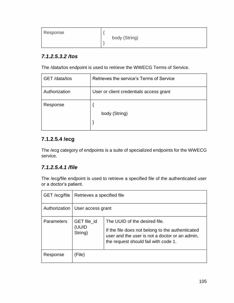
105
Response body (String)
7.1.2.5.3.2 /tos
The /data/tos endpoint is used to retrieve the WWECG Terms of Service.
GET /data/tos Retrieves the service’s Terms of Service
Authorization User or client credentials access grant
Response
body (String)
7.1.2.5.4 /ecg
The /ecg category of endpoints is a suite of specialized endpoints for the WWECG
service.
7.1.2.5.4.1 /file
The /ecg/file endpoint is used to retrieve a specified file of the authenticated user
or a doctor’s patient.
GET /ecg/file Retrieves a specified file
Authorization User access grant
Parameters GET file_id
(UUID
String)
The UUID of the desired file.
If the file does not belong to the authenticated
user and the user is not a doctor or an admin,
the request should fail with code 1.
Response (File)
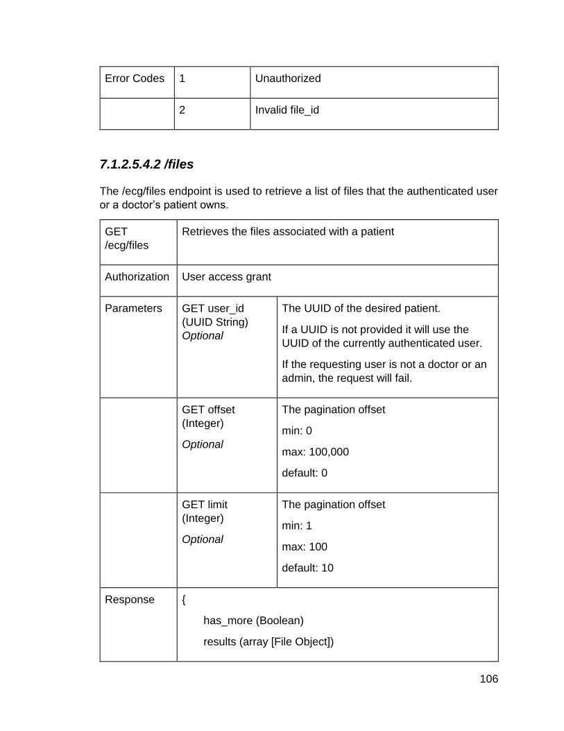
106
Error Codes 1 Unauthorized
2 Invalid file_id
7.1.2.5.4.2 /files
The /ecg/files endpoint is used to retrieve a list of files that the authenticated user
or a doctor’s patient owns.
GET
/ecg/files
Retrieves the files associated with a patient
Authorization User access grant
Parameters GET user_id
(UUID String)
Optional
The UUID of the desired patient.
If a UUID is not provided it will use the
UUID of the currently authenticated user.
If the requesting user is not a doctor or an
admin, the request will fail.
GET offset
(Integer)
Optional
The pagination offset
min: 0
max: 100,000
default: 0
GET limit
(Integer)
Optional
The pagination offset
min: 1
max: 100
default: 10
Response
has_more (Boolean)
results (array [File Object])
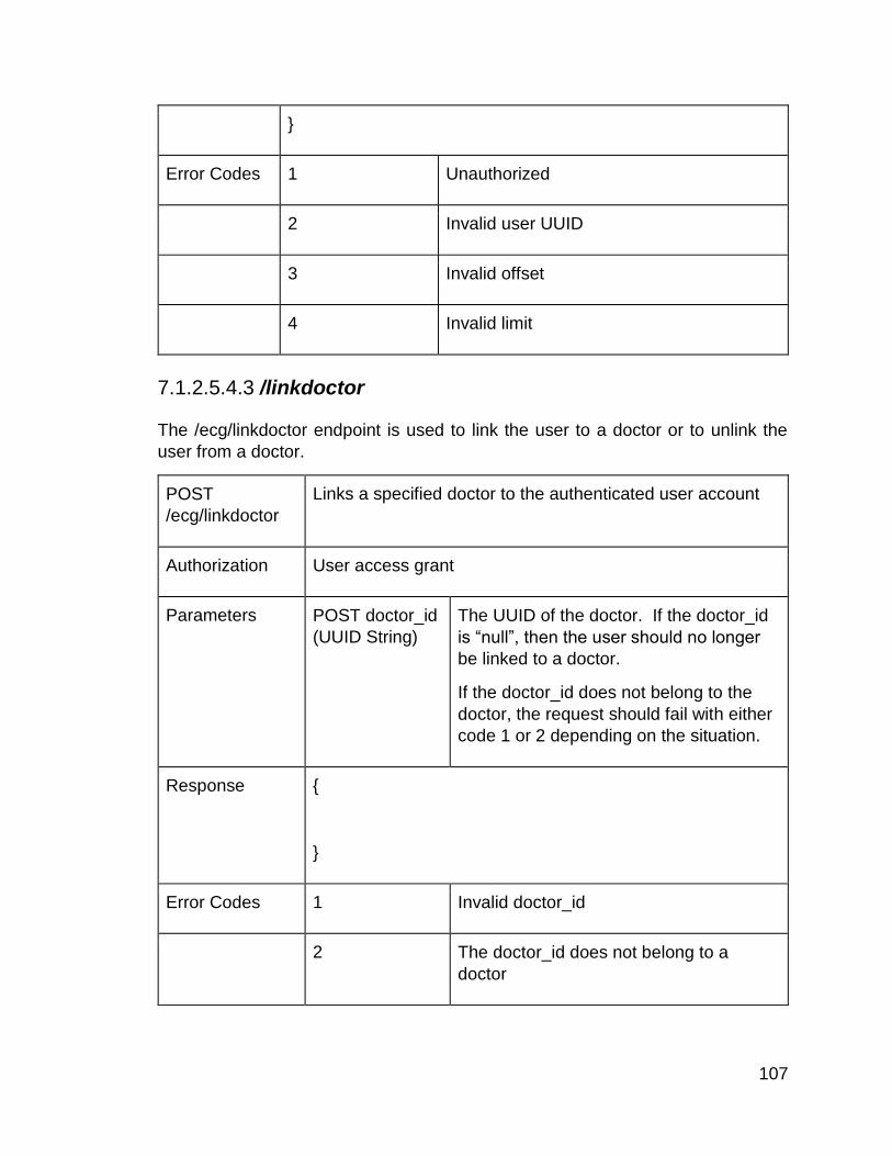
107
Error Codes 1 Unauthorized
2 Invalid user UUID
3 Invalid offset
4 Invalid limit
7.1.2.5.4.3 /linkdoctor
The /ecg/linkdoctor endpoint is used to link the user to a doctor or to unlink the
user from a doctor.
POST
/ecg/linkdoctor
Links a specified doctor to the authenticated user account
Authorization User access grant
Parameters POST doctor_id
(UUID String)
The UUID of the doctor. If the doctor_id
is “null”, then the user should no longer
be linked to a doctor.
If the doctor_id does not belong to the
doctor, the request should fail with either
code 1 or 2 depending on the situation.
Response
Error Codes 1 Invalid doctor_id
2 The doctor_id does not belong to a
doctor

108
7.1.2.5.4.4 /patients
The /ecg/patients endpoint retrieves the patients of the currently authenticated
doctor. If the current user is not a doctor, then this call will fail.
GET /ecg/patients Retrieves the patients of the currently authenticated
doctor
Authorization User access grant
The authenticated user must be an admin or a doctor
An admin will retrieve all users in the system
Parameters GET offset (Integer)
Optional
The pagination offset
min: 0
max: 100,000
default: 0
GET limit (Integer)
Optional
The pagination offset
min: 1
max: 100
default: 10
Response
has_more (Boolean)
results (array [User Object])
Error Codes 1 Insufficient privileges
2 Invalid user UUID
3 Invalid offset
4 Invalid limit

109
7.1.2.5.4.5 /upload
The /ecg/upload endpoint retrieves enables users to upload WWECG sessions to
the WWECG Service. If necessary, this endpoint may be designed to delegate
post processing of WWECG sessions. In this case it will alter the file and
essentially make annotations in the file to mark metrics and features of the
WWECG session. Metrics and features may include: beats per minute,
identification of the Q, R, and S peaks, identification of atrial fibrillation, and
identification of irregular heartbeat.
POST
/ecg/upload
Retrieves the patients of the currently authenticated doctor
Authorization User access grant
If the authenticated user is an admin or a doctor, they can
store the WWECG Session on the behalf of a patient.
Parameters POST patient_id
(UUID String)
Optional
The patient’s UUID to store the file on
behalf of.
If the authenticated user is not an admin
or a doctor, a code 1 error should be
issued.
(Multi-Part Form
Data)
A binary file of the WWECG session.
Response
(File Object)
Error Codes 1 Unauthorized
2 Invalid user UUID
3 Invalid file
4 Processing error

110
7.1.2.5.5 /user
The /user category of the API is for endpoints used to get information of users.
7.1.2.5.5.1 /whoami
The /user/whoami endpoint gives the client information about the currently
authenticated user.
GET /user/whoami Retrieves the currently authenticated user’s information
Authorization User access grant
Response
(User Object)
7.1.2.5.5.2 /whois
The /user/whois endpoint gets information about other users that use the
WWECG service.
7.1.2.5.5.2.1 By Username
This version of the /user/whois endpoint will get the user information of the user
whose name was provided.
GET
/user/whois
Retrieves the specified user’s information
Authorization User access grant
The authenticated user must be an admin or a doctor
Parameters GET email (Email
String)
The name of the user you want
information about
Response
(User Object)

111
Error Codes 1 Invalid email
2 Insufficient privileges
7.1.2.5.5.2.2 By User UUID
This version of the /user/whois endpoint will get the user information of the user
who’s UUID was provided.
GET
/user/whois
Retrieves the specified user’s information
Authorization User access grant
The authenticated user must be an admin or a doctor
Parameters GET id (UUID
String)
The UUID of the user you want
information about
Response
(User Object)
Error Codes 1 Invalid UUID
2 Insufficient privileges
7.1.2.6 Data Objects
This section describes the commonly used JSON objects mentioned in section
7.2.5.
7.1.2.6.1 File
The File object contains meta information on a file on the server. This is the
client facing representation of a /file record.
id (UUID String)
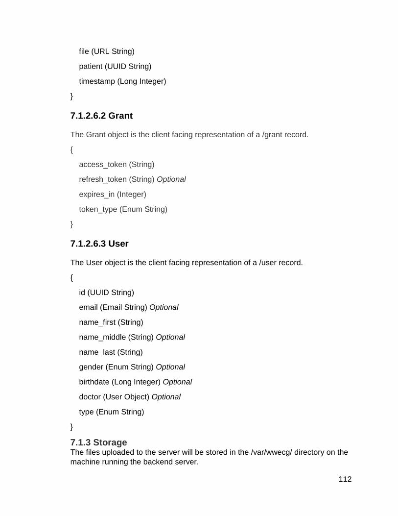
112
file (URL String)
patient (UUID String)
timestamp (Long Integer)
7.1.2.6.2 Grant
The Grant object is the client facing representation of a /grant record.
access_token (String)
refresh_token (String) Optional
expires_in (Integer)
token_type (Enum String)
7.1.2.6.3 User
The User object is the client facing representation of a /user record.
id (UUID String)
email (Email String) Optional
name_first (String)
name_middle (String) Optional
name_last (String)
gender (Enum String) Optional
birthdate (Long Integer) Optional
doctor (User Object) Optional
type (Enum String)
7.1.3 Storage
The files uploaded to the server will be stored in the /var/wwecg/ directory on the
machine running the backend server.

113
7.3 WECG Client Specifications
This section entails the specifications of the Android client to be used with the
WWECG. The app will be compatible with Android 4.4 and up. The app will be
designed with Google’s Material Design Guidelines in mind.
7.3.1 Screens
This section entails the specifications of each screen of the application. These
specifications include: The screen name, on-screen components, user actions, the
activity’s parent activity, and general details explaining what the screen’s main
functions are. For simplicity, the words ‘Screen’ and ‘Activity’ will be used
interchangeably in this section, but as a developer’s note: A ‘Screen’ is a layout or
a collection of UI layouts that make up an activity’s UI, while an activity is a
microprogram that controls the screen UIs. For this app, each screen will map to
one activity. A complete application flow diagram is provided in Figure X.1.
7.3.1.1 Start Screen
The Start Screen is the first screen that a user is shown upon launch of the app. It
provides the user with a means to login or to register with the WWECG
service. The Start Screen does not have a parent activity. Table 7.3.1.1 contains
the required UI components for the Start Screen.
Type ID Description
Button btnLogin A button that starts the Login Activity
Button btnRegister A button that starts the Register Activity
Table 7.3.1.1 - Start Screen UI Components
7.3.1.2 Login Screen
The purpose of the Login Screen is to enable the user to login to the WWECG
Service. The Login Screen is accessible from the start screen. The parent activity
of the Login Activity is the Start Activity.
Type ID Description
EditText txtUsername A textbox for collecting the user’s username.

114
EditText txtPassword A textbox for collecting the user’s password. The
contents of this box should be hidden.
Button btnLogin A button that will attempt to log the user into the
WWECG service. Upon failure, a Toast with an error
message will be displayed. Upon success, the Login
Activity will close and return to the Start Screen where
the start screen will close and launch the Link ECG
Activity.
Table 7.3.1.2 - Start Screen UI Components
7.3.1.3 Register Screen
The Register Screen is used by the user to create a new account for the WWECG
Service. The Register Activity is accessible from the Start Screen. The parent
activity of the Register Activity is the Start Activity.
Type ID Description
EditText txtUsername A textbox for collecting the user’s username.
EditText txtPassword1 A textbox for collecting the user’s password. The
contents of this box should be hidden.
EditText txtPassword2 A textbox for verifying the user’s password. The
contents of this box should be hidden.
EditText txtEmail A textbox for collecting the user’s email address.
Spinner txtGender A combobox that contains Male, Female, or Other
Spinner txtNameFirst A textbox for collecting the user’s first name.
Spinner txtNameMiddle An optional textbox for collecting the user’s middle
name.
Spinner txtNameLast A textbox for collecting the user’s last name.

115
Chooser btnBirthdate A chooser for collecting the user’s birthdate.
Button btnRegister A button that will attempt to create a new user
account in the WWECG service. Upon failure, a
Toast with an error message will be displayed. Upon
success, the Register Activity will close and return to
the Start Screen where the start screen will close and
launch the Link ECG Activity.
Table 7.3.1.3 - Start Screen UI Components
7.3.1.4 ECG Screen
The ECG Screen is used by the user view and playback ECG sessions. It should
be considered the Main Screen of the WWECG app. The ECG Activity may be
started from the Link ECG Activity, or the Start Activity depending on the
situation. The ECG Activity does not have a parent activity.
Type ID Description
ECGDisplay ecg The ECG display. This is a custom UI
component to display a WWECG session on.
Action Bar
Button
menuOptions The button to launch the Settings Activity.
Action Bar
Button
menuLoad A button to replay a saved WWECG session.
Action Bar
Button
menuRecord A button to stop/stop recording a WWECG
session.
Button btnPlay This button will start a previously recorded
WWECG session or a currently active
WWECG session.
Button btnPause This button will pause a previously recorded
WWECG session or a currently active
WWECG session.

116
Spinner txtPatientSelector If the authenticated user is a doctor, a
combobox will appear with a list a patients that
the doctor can select from. This allows the
doctor to select what patients to load and save
the WWECG sessions from. A doctor may
select himself.
Table 7.3.1.4 - ECG Screen UI Components
7.3.1.5 Settings Screen
The Settings Screen is used by the user to set up certain aspects of the app. The
Settings Activity is started from the ECG Activity. The Settings Activity’s parent
activity is the ECG Activity.
Type ID Description
List Item itemLinkWWECG Will launch the Link WWECG Activity.
List Item itemLinkDoctor Will launch the Link Doctor Dialog.
Table 7.3.1.5 - Settings Screen UI Components
7.3.1.6 Link WWECG Screen
The Link WWECG Screen is used by the user to link the WWECG to the app. The
Link WWECG Activity is started from the Settings Activity or the Start Activity
depending on the situation. If the Link WWECG Activity was started by the Options
activity, the Link WWECG’s parent activity is the Options Activity; if it was launched
by the Start Activity, it will not have a parent activity.
Type ID Description
ListView list List items contain the Bluetooth devices in the area. The items
will contain the device MAC and the device name.
Table 7.3.1.6 - Link WWECG Screen UI Components
7.3.1.7 Link Doctor Dialog
The Link Doctor Screen is used by the user to link the user account to a
doctor. The Link Doctor Dialog is started from the Settings Activity.

117
Type ID Description
EditText txtDoctor The textbox to input the doctor’s username or id into.
Button btnOk When pressed, the app will attempt to link the doctor to
the user. If successful the dialog will close with a Toast
saying that the doctor was linked successfully. If there
was an error a toast will display the error.
Button btnCancel When pressed, the dialog will close.
Table 7.3.1.7 - Link Doctor Dialog UI Components
7.3.2 Custom UI Components
Any Android UI components (Views) that need to be made from scratch will be
documented in this section.
7.3.2.1 EcgDisplay
The EcgDisplay view will be used to display both live sessions and previously
recorded sessions stored on the WWECG Server. The display will include an
active ECG Graph, a section for metrics and warnings such as beats per minute
or a warning for an abnormal heartbeat. The display will also be able to display
highlights of the Q, R, and S peaks for easy human analysis of the ECG.
7.3.3 WWECG Bluetooth Link
The app will communicate with the WWECG Hub over Bluetooth LE. The app will
use Android’s internal libraries to communicate with the WWECG Hub. The GATT
ids to be used to communicate between the app and the WWECG Hub are TBD.
7.3.4 WWECG Server Link
The app will communicate with the WWECG Service using the Application
Programming Interface that is documented in Section 7. The app will use the
HTTPSConnection class as a tool to easily make HTTPS calls to interface with the
API. The server link will be implemented inside of the WwecgAPI class.
7.3.5 WWECG Live Processing

118
Live processing of WWECG sessions will be done. The app will analyze the data
that is taken from the WWECG and look for certain metrics and features. Some of
the features may not be included in the final product. Metrics and features must
include: Beats per minute and highlighting of the Q, R, S peaks. Metrics and
features may include the identification of atrial fibrillation and the identification of
irregular heartbeat. If processing of certain metrics prove to be too intensive for
the device, then these metrics and features may be processed on the WWECG
server instead of the user’s device, however, this is TBD.
7.4 Storage
The files uploaded to the server will be stored in the /var/wwecg/ directory on the machine running the backend server.
8 Administrative Information
The following sections below describe what methods that will be used throughout
the development process. Featuring our project management methods, cost
analysis, facilities, personal, current work completed and future WWECG
milestones, these sections give an insight analysis of the project from a
management rather than technical viewpoint.
8.1 Project Management Methodology
In order to stay organized throughout the development process, it was determined
that the best way to keep the project on schedule as well as prepare group
members for real world development lifecycles was to use an Agile-Scrum based
project management platform. Using Google Sheets together with Scrum allowed
the group to easily view the task needed to be completed at week as well as
decrease procrastination.
8.2 Material Cost Analysis
The table below displays the estimated cost that will incur during the construction
of the WWECG project.
Table 8.2.1 –Parts List
Part Cost
Adafruit Resistor and Capacitor Book $39.95
SOIC-DIP adapter $10.00
4x Bluetooth HM-11 BLE modules $51.60
Adafruit5 V switching power supply for HUB $7.95

119
4x 150 mAh Li-ion Polymer batteries $23.80
2x USB Li-Ion charger modules $25.00
6x LM2663 Voltage converter $15.12
10x TL084 Quad JFET op amps $6.40
6x LM2621 Step up DC-DC converter $13.08
2x INA333 Instrumentation amplifier $9.00
2x TMS320 Digital signal processor $6.68
2x DAC8411 $8.06
3xADC1251 $33.42
2x MSP430F5438AIPZ $10.00
1x MSP432P401R $7.60
Estimated cost of PCB manufacturing $150.00
Total Parts Cost: $417.66
8.3 Facilities and Equipment
The development of the Wireless Wearable Electrocardiogram will primarily take place at the Electrical Engineering Senior Design Lab at the University of Central Florida. This location will provide breadboards and other electrical components useful for early design prototyping. Additionally, it will provide a housing location for the project so we do not have to transfer it back and forth often. The senior design lab also contains important lab equipment such as oscilloscopes, multimeters, function generators, and power supplies. Each of these pieces of equipment are key for testing and designing our project. Furthermore, this facility has a soldering location that will be employed to solder the surface mount components onto our printed circuit boards in the final design stages. Lastly, this location has key software that will be used to analyze and simulate circuits or software to make sure the actual implementation of our devices behave as expected.
8.4 Personnel
Ulbert J. Botero Major: Electrical Engineering Minor: Computer Science Design Contributions: For the Wireless Wearable Electrocardiogram Ulbert Botero mainly focused on the signal processing and analog front end design. He designed the signal acquisition/conditioning circuit which consisted of 60Hz filtering, motion artifact

120
filtering, and antialiasing filtering. Additionally, he assisted with the development of the overvoltage and overcurrent protection circuit to protect the electronics from possible defibrillator contact. Lastly, Ulbert implemented the signal processing algorithms to determine QRS complexes, heart rate, and warn of arrhythmias on the digital signal processor. Alexander Consunji Major: Computer Engineering Design Contributions: Alexander Consunji's role in the Wireless Wearable Electrocardiogram primarily focused on the communication between boards via Bluetooth and embedded systems programming. In addition, he had the job of interfacing the Analog-to-Digital and Digital-to-Analog converters with the embedded microcontrollers. Lastly, Alex designed the synchronization method to ensure the wireless wrist sensors sampled the biopotential signals at the same moments and transmitted them in unison. Ryan Shifman Major: Electrical Engineering Design Contributions: Ryan Shifman assisted with the development of the Analog Front End and defibrillator protection circuitry. His primary focus was power management of the wearable devices and the central Hub. This consisted of determining the charging method for the wrist sensors, the proper battery to employ for the hub and sensors, and how to power the Hub. Ryan was responsible for PCB layout design and soldering surface mount components along with circuit simulation and schematic capture. Karson Kimbrel Major: Computer Science Design Contributions: Karson Krimbrel’s key contributions to the project consists in most of the dedicated software. In charge of all software design and implementation, Karson’s expertise focus on the Android application and utilizing the operating system to connect with Bluetooth modules in the system. Karson is also heading the data storage and server design. Karson also have extensive experience with radio frequency transmissions and collaborates with other group members in dealing with possible wireless interference.
8.5 Past Activity Levels
Below lists a copy of the tasks that have been completed throughout Senior Design
1. This data was recorded using Google Sheets

121
Week Main Item Assigned To
In progress
Completed By
Date Completed Results
9/6/2015
Initial Document-Divide and Conquer(Webcourses)
All 9/14/2015
Submitted online webcourses
Alex Alex 9/10/2015
Alex
Alex
All
Ryan and Joey
Ryan and Joey 9/10/2015
Completed See Divide and Conquer
Attempt email Dr. Kapoor Again?
Meet with Optical Engineer?
Finalize Idea between BGM and ECG/EKG
All All 9/10/2015
Finalized were going with ECG/EKG wireless implementation
Email Heinrich for possible CS group member
Ryan Ryan
Finish proposal and submit it to webcourses
Email Richie about new group member
Ryan Ryan
Tell Richie we no longer need optical engineer
9/12/15 --Sponsorship meeting
Ryan and Alex
Ryan and Alex 9/12/2015
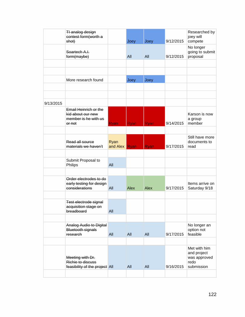
122
TI analog design contest form(worth a shot)
Joey Joey 9/12/2015
Researched by joey will compete
Soartech A.I. form(maybe)
All All 9/12/2015
No longer going to submit proposal
More research found Joey Joey
9/13/2015
Email Heinrich or the kid about our new member is he with us or not Ryan Ryan Ryan 9/14/2015
Karson is now a group member
Read all source materials we haven’t
Ryan and Alex Ryan Ryan 9/17/2015
Still have more documents to read
Submit Proposal to Philips All
Order electrodes to do early testing for design considerations All Alex Alex 9/17/2015
Items arrive on Saturday 9/18
Test electrode signal acquisition stage on breadboard All
Analog Audio to Digital Bluetooth signals research All All All 9/17/2015
No longer an option not feasible
Meeting with Dr. Richie to discuss feasibility of the project All All All 9/16/2015
Met with him and project was approved redo submission

123
Redo design and submit proposal to Phillips and other companies All
All
All All 9/17/2015
9/20/2015
Finish redoing block diagram All All All 9/24/2015
New block diagram is now done along with revised divide and con
Resubmit finalized design and conquer to Richie and submit to Philips All All
9/24/2015
Decide on parts we want to order and design aspects the add them to part list All All
Next Week
Create list of HIPAA limitations All Karson Karson 10/1/2015
Email Richie with new proposal and documents All Alex Alex 9/25/2015
9/27/2015
Parts List Actually get Done All
O-Scope Functionally Reading Example All All
Ryan and Joey 10/29/2015
Design considerations All All All 10/9/2015
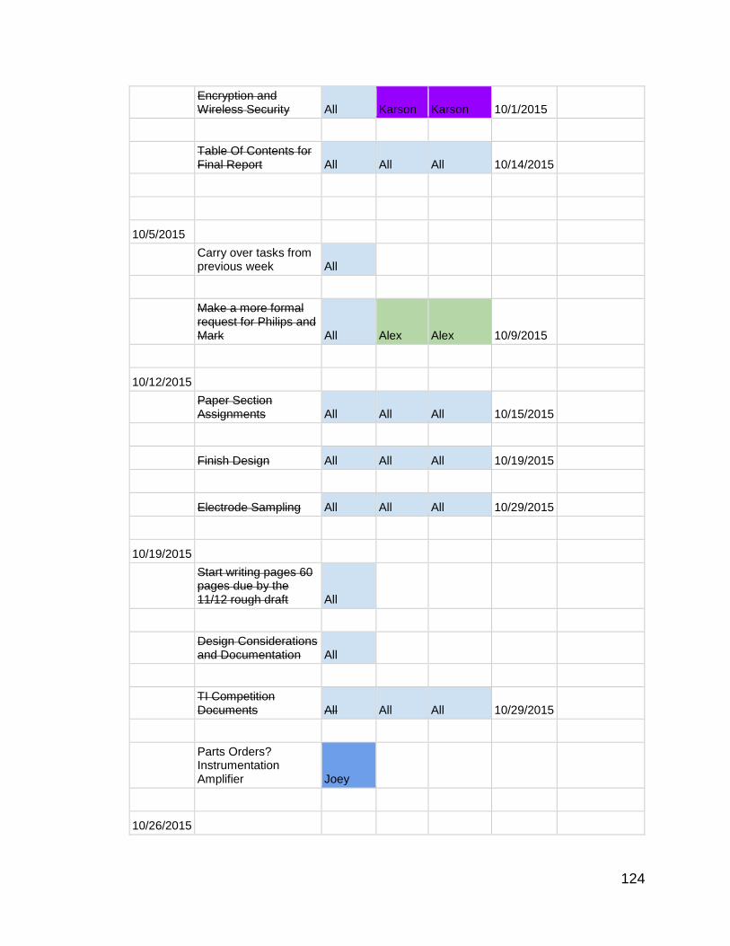
124
Encryption and Wireless Security All Karson Karson 10/1/2015
Table Of Contents for Final Report All All All 10/14/2015
10/5/2015
Carry over tasks from previous week All
Make a more formal request for Philips and Mark All Alex Alex 10/9/2015
10/12/2015
Paper Section Assignments All All All 10/15/2015
Finish Design All All All 10/19/2015
Electrode Sampling All All All 10/29/2015
10/19/2015
Start writing pages 60 pages due by the 11/12 rough draft All
Design Considerations and Documentation All
TI Competition Documents All All All 10/29/2015
Parts Orders? Instrumentation Amplifier Joey
10/26/2015

125
Carry over all tasks from previous weeks
11/1/2015 Continue Carry over All All All
Order Op Amps, Instrumentation Amp, Decide on MCU All All All 11/8/2015
Test and Use HM-11 Alex Alex Alex
Test A/D All All All 11/8/2015
11/8/2015 Finish Rough Draft All All All 11/11/2015
11/15/2015 Write for final Draft
11/22/2015 Continue Writing
11/29/2015 Continue Writing
12/6/2015 Edit Writing All All All 12/5/2015
Professionally Bind and Submit Final Report All All All 12/9/2015
8.6 Future Milestone Chart
Week 1:
Hardware:
-Prototype Analog Front End for each sensor and test.
-Start mocking up a printed circuit board in eagle for wristbands.

126
-Test data being sent across devices between Bluetooth on test microcontrollers
Software:
-The LAMP stack and security certificate should be installed on the server.
-Begin embedded software design for the hub to broadcast and timestamp.
Week 2:
Hardware:
-Continue to condition signal. Compare accuracy of AFE sensor to traditional ECG
using ECG signal simulator, test Analog-to-Digital conversion.
-Test Bluetooth transmission with multiple slaves from a single master and
prototype Hub.
-Start mocking up a printed circuit board in eagle for the hub. Verify power
conditions and increase battery capacity if necessary.
Software:
-Create the MySQL tables. Start work on the /auth/ section of the server
endpoints.
-Begin testing sending two times consistently to two separate serial test devices
with the same timestamp
Week 3:
Hardware:
-Have Bluetooth transmission successful, Digital-to-Analog Conversion accurate,
and compare final result after Instrumentation Amplifier.
-Test Charging and housing of sensors at Hub.
Software:
-All /users/, /data/, and /auth/ endpoints should be finished.
Week 4:
Hardware:
-Fabricate PCB for wrist sensors and HUB by uploading eagle designs to Osh
Park.
Software:
-The /ecg/ section of server endpoints should be finished (with the exception of the
/auth/upload post processing of files).

127
-Complete software for hub transmitting startup items via serial
Week 5:
Hardware:
-Begin soldering surface mount parts to the printed circuit boards
-Manufacture enclosures for wrist sensors and Hub PCBs.
Software:
Implement Signal Processing Algorithms on DSP.
-The start, login, and register screens of the app should be finished
Week 6:
Hardware:
-PCBs should be completed and components soldered for sensors and Hub.
Software:
-Test Signal Processing Algorithms.
-The Link WWECG Screen and the ECG Screen should be started.
Week 7:
Hardware:
-Hardware should be completed.
Software:
-Test communication with mobile application, and transmission of key information
from signal processing algorithms.
-The Settings Screen and the Link Doctor Screen should be finished.
Week 8:
Hardware: Complete
Software:
-Test mobile application display of information and database.
-Link WWECG Screen and the ECG Screen should be finished.
Week 9:
Hardware:

128
-Test Complete System, determine any improvements that can be made to final
design in a timely manner, add another sensor if possible.
Software:
-Test Complete System, determine any improvements that can be made to final
design in a timely manner.
Week 10:
Present Final Product.
9 Construction and Testing
The following subsections review how the project integrates and will be tested in
order to meet all standards and requirements.
9.1 Chipset Integration
The cost of parts differs depending on package size, for prototyping it is more cost
efficient to purchase or obtain free samples from Texas Instruments in a SOIC pin
package than a DIP package. For this reason many of the parts used in testing
were SOIC package components soldered onto a SOIC-DIP adaptor board. The
op amps used in the signal acquisition stage were reused from previous labs and
were fortunate enough to be DIP components.
Figure 9.1 – SOIC to DIP adapter

129
9.2 PCB Design
Eagle PCB by Cadsoft will be used as the primary software for printed circuit board
layout.
9.3 PCB Manufacturing
The printed circuit boards for the WWECG will be manufactured by OSH Park
using the PCB design layout uploaded to their website. Osh Park is the most cost
efficient for this particular design. Osh Park’s standard 2 layer printed circuit board
starts at $5.00 per square inch and comes with three copies. Having three copies
of a circuit board is beneficial in reducing costs in that both wristbands will
incorporate the same exact PCB.
Components will be either reused from the prototyping phase or will be ordered
through Texas Instruments, Digi-key, Adafruit or Mouser depending on surface
mount part availability. It is more cost efficient to purchase a surface mount resistor
kit and capacitor kit that provide various values and order separately if the kits do
not provide all values needed.
The final design will be hand soldered using a PACE Worldwide adjustable
temperature soldering machine in an electrostatic discharge (ESD) safe
environment on top of an ESD mat provided by the place of employment of one of
the design team members. The benefit of using an adjustable temperature
soldering machine is that some components list different soldering temperatures
and contact times as they may be delicate.
9.4 ECG Signal Quality
The quality of the signal obtained should be accurate and comparable to standard
ECG signals. For this reason the design of the WWECG has been centered on
reducing as much outside noise as possible.
9.5 Level of Comfort
One of the primary concerns at the conception of the WWECG was the comfort
and portability of the design. The intention was to design a functional ECG that
optimized portability without compromising comfort levels for the user. For this
reason the design was based on reducing size and weight of components so the
research stage was important in finding low power components that would reduce
the amount of power used with each diagnosis thus reducing the size of the battery
packs needed to power the components. Figure 9.5 exhibits the size of ICs used
compared to a US quarter.

130
Figure 9.5 – Size comparison of SOIC chips on DIP adapter board
9.6 Testing Procedures
Overall testing throughout the projects implementation phase will be done by using
a unit testing format for both software and hardware integration. The choice to use
unit testing stems from the easy of which debugging will be done. For software
testing proper unit tests provides simpler viewpoint when searching for bugs that
may have occurred within different levels. Hardware also benefits from unit testing
in regards for its ability to isolate issues that occur within the boards and their parts.
9.6.1 Hardware Testing
Testing of the sensors was done using a breadboard so DIP components were
favored for their convenience. Figure 9.6.1 shows the prototype signal acquisition
stage of two sensors on a breadboard
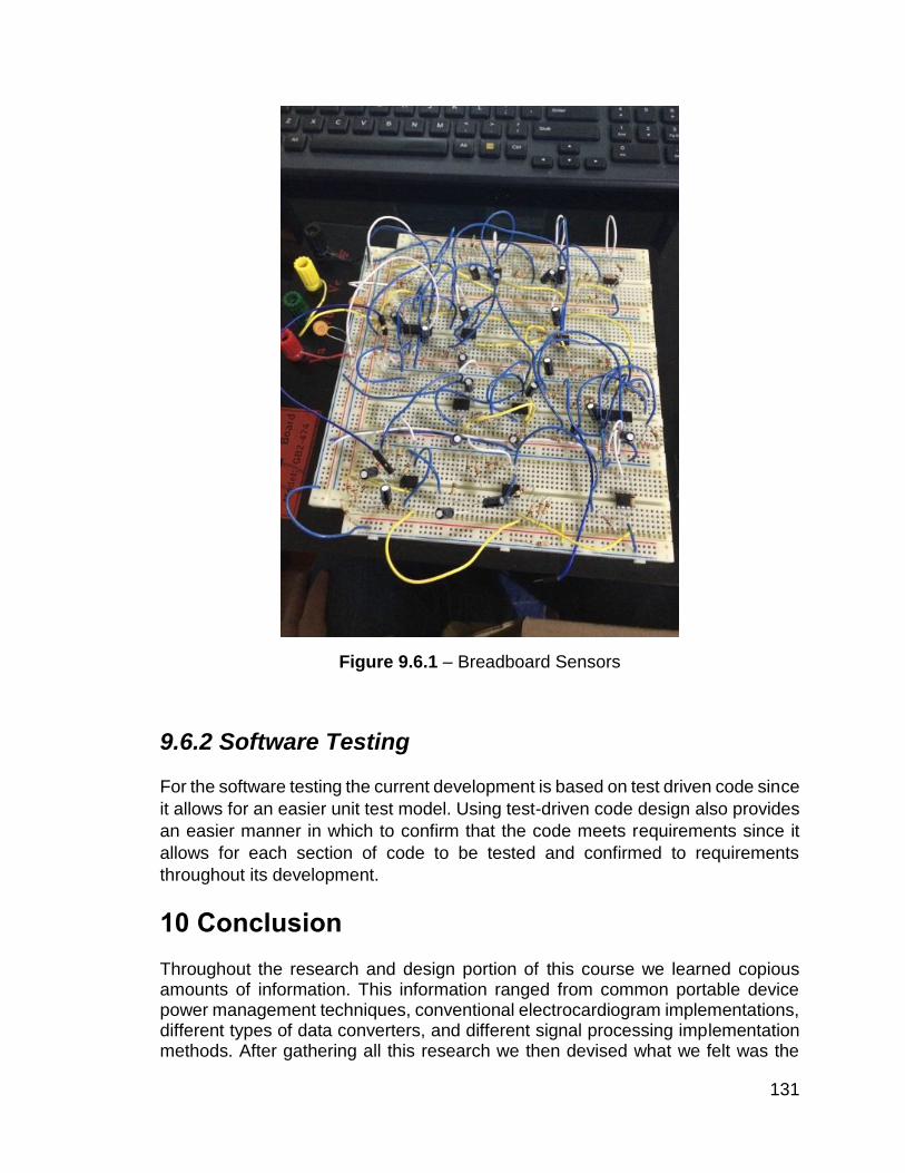
131
Figure 9.6.1 – Breadboard Sensors
9.6.2 Software Testing
For the software testing the current development is based on test driven code since
it allows for an easier unit test model. Using test-driven code design also provides
an easier manner in which to confirm that the code meets requirements since it
allows for each section of code to be tested and confirmed to requirements
throughout its development.
10 Conclusion
Throughout the research and design portion of this course we learned copious amounts of information. This information ranged from common portable device power management techniques, conventional electrocardiogram implementations, different types of data converters, and different signal processing implementation methods. After gathering all this research we then devised what we felt was the

132
best plan of attack to make a completely wireless wearable electrocardiogram sensing device. There were many considerations that were taken in choosing our device. We began the project with the goal of making an accurate, comfortable, and portable device. Therefore, our design had to include small scale, low power electronics to maintain portability and comfort. Additionally, in order to maintain accuracy we used high accuracy data converters with extensive front end analog signal processing. Another issue we had to consider was developing this product at a reasonable price. Since we do not have a sponsor at the moment we mainly focused on using Texas Instruments products due to their affordability for our budget range while still maintaining high accuracy and fidelity. This project was a great exercise in putting all the theory learned in the classroom throughout our undergraduate curriculum into practice to design a final product. The next step will be to build a functional prototype of our design and adjust to any problems that could arise from possible design issues we may have overlooked. If we are fortunate enough to not run into any such issues the next logical step will naturally be to improve it. Even when the initial design is produced an engineer's job is never truly done.

133
11 APPENDIX A- Copyright Permission
Permission of use
Nicholas Patchett MD.
March 27th 2015
The author of this work does not endorse me or the use of my work.

134
12 APPENDIX B- References
Riggs, T., B. Isenstein, and C. Thomas. "Result Filters." National Center for
Biotechnology Information. U.S. National Library of Medicine, n.d. Web. 05 Nov.
2015.
Narayanaswamy, S. "High Resolution Electrocardiography." Indian Pacing and
Electrophysiology Journal. Indian Pacing and Electrophysiology Group, 1 Apr.
2002. Web. 06 Nov. 2015.
Winter, Bruce B., and John G. Webster. "Driven-right-leg Circuit Design." IEEE
Transactions on Biomedical Engineering IEEE Trans. Biomed. Eng. BME-30.1
(1983): 62-66. Web.
Texas Instruments. Improving Common-Mode Rejection Using the Right-Leg
Drive Amplifier, Sbaa188 - TI.com. Improving Common-Mode Rejection Using
the Right-Leg Drive Amplifier, Sbaa188 - TI.com. Texas Instruments, n.d. Web.
09 Nov. 2015.
Pan, Jiapu, and Willis J. Tompkins. "A Real-Time QRS Detection Algorithm."
IEEE Transactions on Biomedical Engineering IEEE Trans. Biomed. Eng. BME-
32.3 (1985): 230-36. Web.
Gari Clifford, John Fisher, Julie Greenberg, and William Wells. HST.582J
Biomedical Signal and Image Processing, Spring 2007. (Massachusetts Institute
of Technology: MIT OpenCourseWare), http://ocw.mit.edu (Accessed 9 Dec,
2015). License: Creative Commons BY-NC-SA
Laumeister, Bill. "Lightning Bolts, Defibrillators, And Protection Circuitry Save
Lives." Lightning Bolts, Defibrillators, And Protection Circuitry Save Lives. N.p.,
n.d. Web. 30 Nov. 2015.
Krois, I., V. Isgum, and M. Cifrek. "The Amplifier Input Protection Circuit for a
Intraoperative Evoked Potential Monitoring System." Proceedings of the 12th
IEEE Mediterranean Electrotechnical Conference (IEEE Cat. No.04CH37521)
(2004): n. pag. Web.
Yanowitz, Frank G., MD. "3. Characteristics of the Normal ECG." ECG Learning
Center. University of Utah School of Medicine, n.d. Web. 25 Nov. 2015.
Ventricular Tachycardia. Ventricular Tachycardia. Blausen Medical, n.d. Web. 3
Dec. 2015.
Zevitz, Michael E., MD. "Ventricular Fibrillation." : Background, Pathophysiology,
Etiology. Medscape, n.d. Web. 5 Dec. 2015.
"Ventricular Fibrillation: MedlinePlus Medical Encyclopedia." U.S National Library
of Medicine. U.S. National Library of Medicine, n.d. Web. 02 Dec. 2015.

135
Thies, Karl-Christian, Karin Boos, Kai Müller-Deile, Wolfgang Ohrdorf, Thomas
Beushausen, and Peter Townsend. "Ventricular Flutter in a Neonate—severe
Electrolyte Imbalance Caused by Urinary Tract Infection in the Presence of
Urinary Tract Malformation." The Journal of Emergency Medicine 18.1 (2000):
47-50. Web.
"Atrial Flutter Information - The Mount Sinai Hospital." The Mount Sinai Hospital.
N.p., n.d. Web. 3 Dec. 2015.
Searle, A., and L. Kirkup. "A Direct Comparison of Wet, Dry and Insulating
Bioelectric Recording Electrodes." Physiol. Meas. Physiological Measurement
21.2 (2000): 271-83. Web.
Oweis, Rami J., and Basim O. Al-Tabbaa. "QRS Detection and Heart Rate Variability Analysis: A Survey." Biomedical Science and Engineering 2.1 (2014): 13-34.
"ADC and DAC." The Scientist and Engineer's Guide to Digital Signal
Processing. Place of Publication Not Identified: Stationery Office, 2006. 35-66.
Print.
"ADI - Analog Dialogue | Data Conversion Handbook." ADI - Analog Dialogue |
Data Conversion Handbook. N.p., n.d. Web. 28 Nov. 2015.
Bluetooth Special Interest Group "Bluetooth Low Energy Regulatory Aspects",
April 2011
Smart Wearable ECG EKG Monitor - QardioCore. (n.d.). Retrieved October 9,
2015, from https://www.getqardio.com/qardiocore-wearable-ecg-ekg-monitor-
iphone/
Delano, Maggie K.; Sodini, Charles G., "A long-term wearable electrocardiogram
measurement system," in Body Sensor Networks (BSN), 2013 IEEE International
Conference on , vol., no., pp.1-6, 6-9 May 2013
URL: http://ieeexplore.ieee.org/stamp/stamp.jsp?tp=&arnumber=6575459&isnum
ber=6575455
Difference between Bluetooth and Zigbee Technologies. (n.d.). Retrieved
December 9, 2015, from http://www.engineersgarage.com/contribution/zigbee-
vs-bluetooth
The Nuremberg Code. (n.d.). Retrieved December 9, 2015, from
http://www.hhs.gov/ohrp/archive/nurcode.html
Retrieved December 9, 2015, from
https://www.students.graduate.ucf.edu/policy/human_subjects_research/
The OAuth 2.0 Authentication Framework https://tools.ietf.org/html/rfc6749

136
13 APPENDIX C- Data Sheets and User Guides
DSP TMS320C5535: http://www.ti.com/product/TMS320C5535/datasheet
ADC ADS1251: http://www.ti.com/lit/ds/sbas184d/sbas184d.pdf
DAC DAC8411: http://www.ti.com/product/DAC8411/datasheet
Instrum. INA333: http://www.ti.com/lit/ds/symlink/ina333.pdf
MCU MSP430F5438: https://www.ti.com/product/MSP430F5438A/datasheet
MCU MSP430F5438: https://www.ti.com/product/MSP432P401R/datasheet
HM-11 BLE Module: http://www.seeedstudio.com/wiki/Bluetooth_V4.0_HM-
11_BLE_Module
TI CC2541: http://www.ti.com/lit/ds/symlink/cc2541.pdf