what if we could assemble the basic ingredients of life the way nature does it, atom by atom and...
TRANSCRIPT


What if we could assemble the basic ingredients of lifethe way nature does it, atom by atom and molecule by molecule?

“What I want to talk about is the problem of manipulating and controlling things on a small scale.”
“Why cannot we write the entire 24 volumes of the Encyclopedia Brittanica on the head of a pin?”
Feynman’s Talk, 1959, Caltech

head of a pin =1/16 inches across
× 25,000 = All the pages of the
Encyclopedia Brittanica
resolving power of a human eye
25,000÷ =
80 Angstroms(32 atoms in ordinary metal)
1/120 inch= diameter of a dot in the Encyclopedia

Feynman’s Talk, 1959, Caltech
“What are the limitations as to how small a thing has
to be before you can no longer mold it? How many
times when you are working on something
frustratingly tiny like your wife's wrist watch, have
you said to yourself, ``If I could only train an ant to
do this!'' What I would like to suggest is the
possibility of training an ant to train a mite to do
this”
Feynman’s Talk, 1959, Caltech
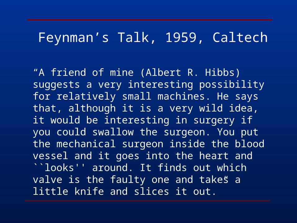
“A friend of mine (Albert R. Hibbs) suggests a very interesting possibility for relatively small machines. He says that, although it is a very wild idea, it would be interesting in surgery if you could swallow the surgeon. You put the mechanical surgeon inside the blood vessel and it goes into the heart and ``looks'' around. It finds out which valve is the faulty one and takes a little knife and slices it out.”
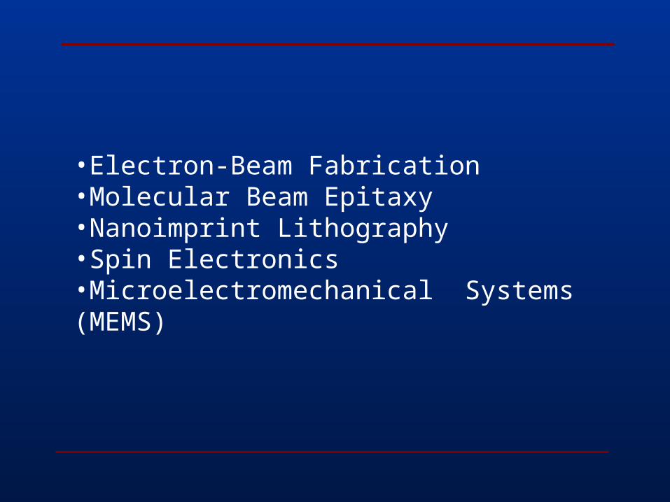
•Electron-Beam Fabrication•Molecular Beam Epitaxy•Nanoimprint Lithography•Spin Electronics•Microelectromechanical Systems (MEMS)

•Nano-Technology first used by N.Taniguchi (1974)•Nanotechnology became popularized afterK.E. Drexler’s book “Engines of Creation” in 1986.

What does Nanotechnology mean?
•“Nano” derives from the greek word for dwarf.•It represents a billionth of a unit.
1nm = billionth of a meter = 10-9 m

How small is a nanometer?

•Some nanotechnology isn’t nano•Nanotechnology, in some cases is not technology•Nanotechnology is a new word but not an entirelynew field.
Nanotechonology: Real or just a buzz word?

•Nano-sized carbon particles used in tires for about100 years•Vaccines, which often consist of one or more proteins with nanoscale dimensions•Chemical catalysts, such as those turning cheapgraphite into synthetic diamond.•Photosynthesis (natural nanotechnology)
Why not an entire new field?

Photosynthesis
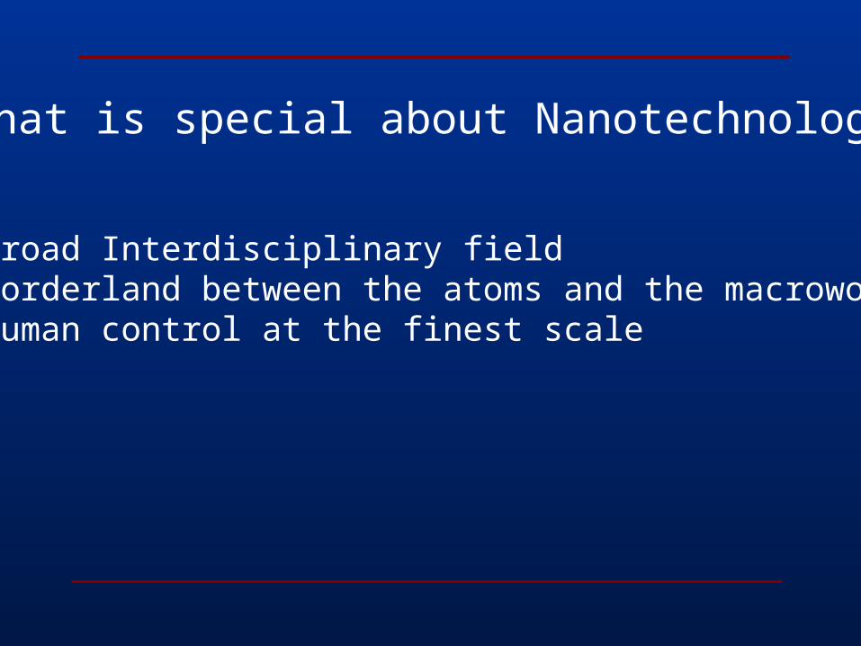
What is special about Nanotechnology?
•Broad Interdisciplinary field•Borderland between the atoms and the macroworld•Human control at the finest scale

Nanotechnology: Is it fiction?

From Fiction to Reality: Skeptical Questions
•Can macroscopic objects be built from molecular scale processes?•Are molecular objects stable?•What about quantum effects?•What about Brownian effects?•What about high-energy radiation?•What about friction and wear?

Nanotechnology does not violate any physical law.

Approaches to Nanotechnology
•Top-Down Approach•Bottom-Up Approach

Top-Down Approach
1/4 1/4
Machine Shop Reduced-ScaledMachine Shop

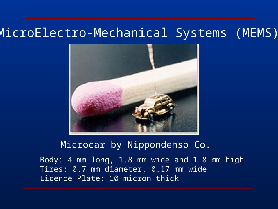
MicroElectro-Mechanical Systems (MEMS)

MicroElectro-Mechanical Systems (MEMS)
MicroElectro-Mechanical Systems (MEMS)
Microcar by Nippondenso Co.
Body: 4 mm long, 1.8 mm wide and 1.8 mm highTires: 0.7 mm diameter, 0.17 mm wideLicence Plate: 10 micron thick
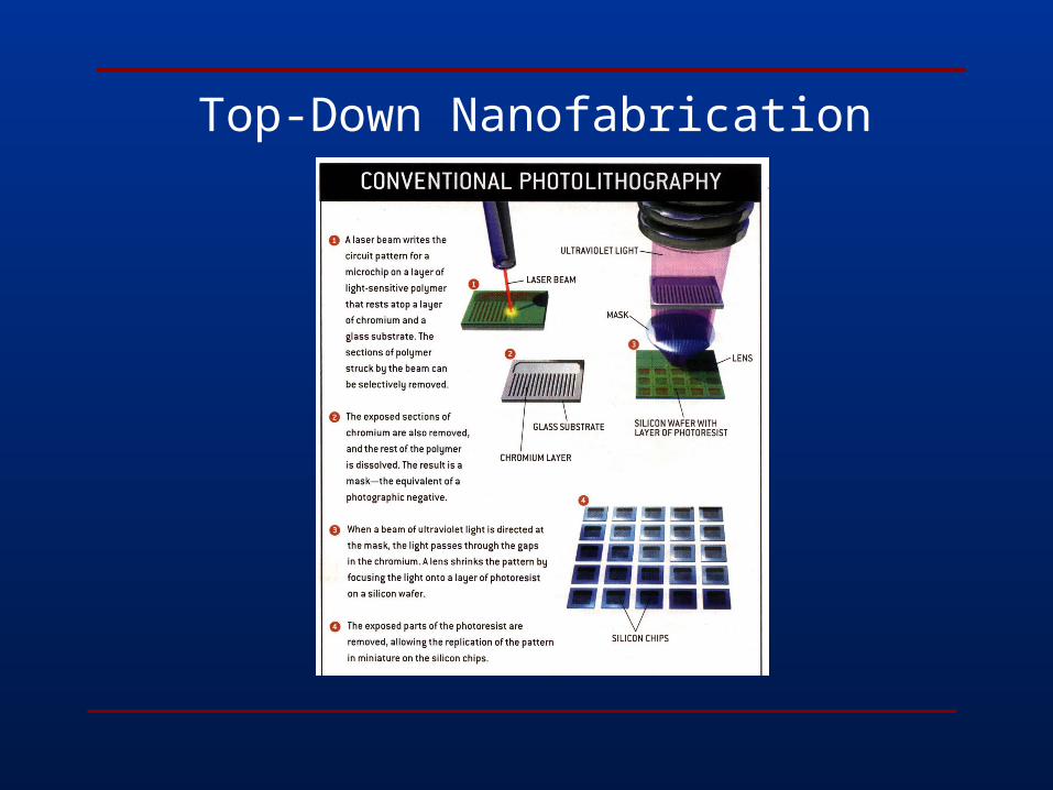
Top-Down Nanofabrication

Top-Down Nanofabrication
Electron Beam Lithography
•Pattern written in a polymer film with a beam of electrons•No blurring of features•Very expensive and time-consuming
X-ray Lithography
•Wavelength = 0.1-10 nm, no blurring•Conventional lenses do not focus X-rays•Radiation damage of materials
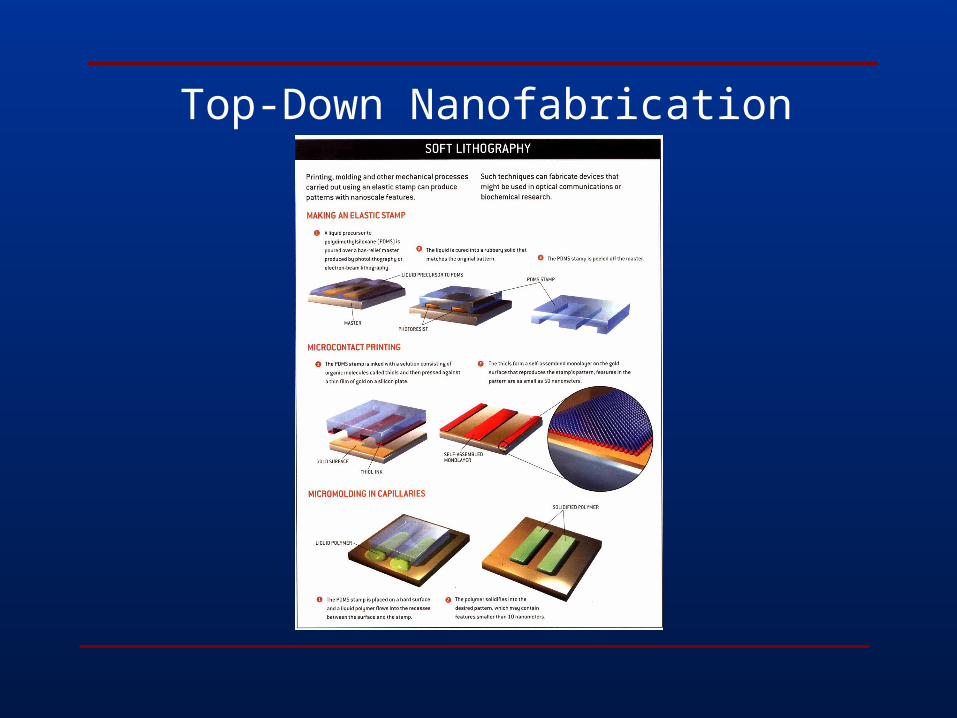
Top-Down Nanofabrication

Bottom-Up Nanofabrication
•Supramolecular and molecular chemistry•Scanning probes•Biotechnology

Supramolecular Chemistry(Chemistry of non-covalent bonds)
Self-Assembly demands:
•Well-defined adhesion between molecules•Shape and size complementarity•Large contact areas•Strong overall binding

Advantages of Self-Assembly
•It carries by itself the most difficult steps in nanofabrication,i.e., the smallest steps•Can incorporate biological structures directly as componentsin the final systems.•Because target structures are thermodynamically stable, itproduces structures that are relatively defect-free and self-healing.

Self-Assembly
Carbon Nanotubes

Growth of C nanotubes
CVD Synthesis
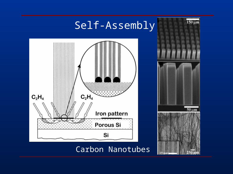
Self-Assembly
Carbon Nanotubes

Structure of C Nanotubes
Single Walled Nanotube Multi Walled Nanotube

Gears of C Nanotubes70 GHz
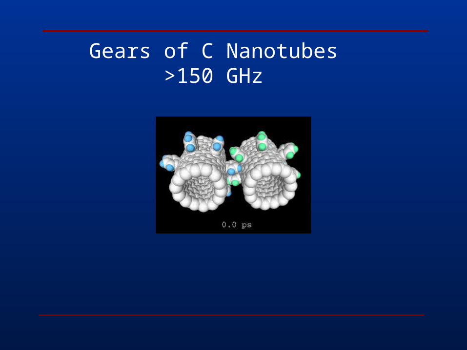
Gears of C Nanotubes>150 GHz

Rack/Pinion C Nanotubes

Quantum Dots

Bottom-Up Nanofabrication
•Supramolecular and molecular chemistry•Scanning probes•Biotechnology

Scanning Probes

Manipulation of Atoms by SP

Atomic Writing by SP

Bottom-Up Nanofabrication
•Supramolecular and molecular chemistry•Scanning probes•Biotechnology

Drexler wrote:
“The ability to design protein moleculeswill open a path to the fabrication ofdevices to complex atomic specfications”

Biotechnology
Biological Molecular Machine: Ribosome
1 large RNA1 small RNA33 proteins
1 RNA21 proteins

Ribosome as an assembler

Abalone
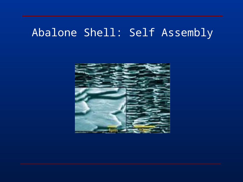
Abalone Shell: Self Assembly

Applications
•Nanodevices•Nanoelectronics•Nanomedicine

Nanodevices
Single-Electron Transistor
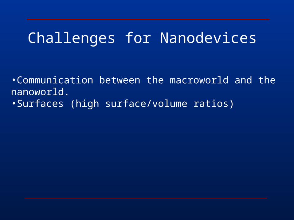
Challenges for Nanodevices
•Communication between the macroworld and the nanoworld.•Surfaces (high surface/volume ratios)

Nanoelectronics
•1st level of organization: transistors•2nd level of organization: interconnects
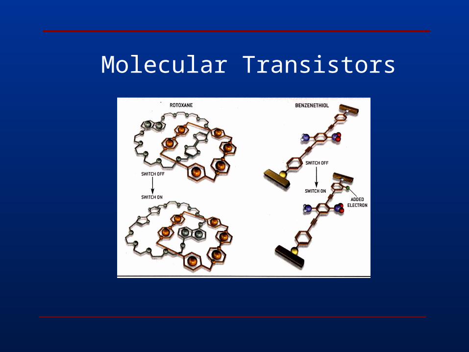
Molecular Transistors

C Nanotube Interconnects
•Wire interconnect delays account for half of chip
signal delays
•Copper interconnects being used for 130nm
devices
•Microelectronic devices being scaled down from
130nm to 50nm generation
•Copper interconnects not suitable for 50nm devices
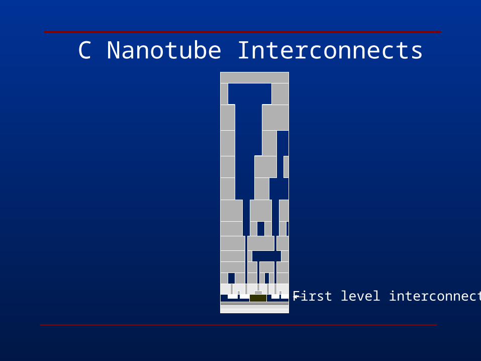
C Nanotube Interconnects
First level interconnect

C Nanotube Interconnects
Single wall nanotube ~ 1.4 nm
Jc = 109 A/cm2
ts ~ 30GPaK ~ 2000W/mK

DNA Computing

Nanomedicine
Magnetic Nanoparticles
NS

Nanomedicine

Nanomedicine

Nanotechnology: A Look to the Future
Fiscal Year
1997 2000 2001 2002
Europe 126 200 225 400
Japan 120 245 465 650
USA 116 270 422 604
Others 70 110 380 500
Total 432 825 1502 2154
Estimated government sponsored R&D in $millions-year
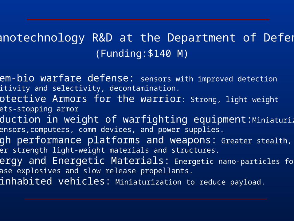
Nanotechnology R&D at the Department of Defense(Funding:$140 M)
•Chem-bio warfare defense: sensors with improved detectionsensitivity and selectivity, decontamination.
•Protective Armors for the warrior: Strong, light-weight bullets-stopping armor
•Reduction in weight of warfighting equipment:Miniaturization of sensors,computers, comm devices, and power supplies.
•High performance platforms and weapons: Greater stealth, higher strength light-weight materials and structures.
•Energy and Energetic Materials: Energetic nano-particles for fastrelease explosives and slow release propellants.
•Uninhabited vehicles: Miniaturization to reduce payload.
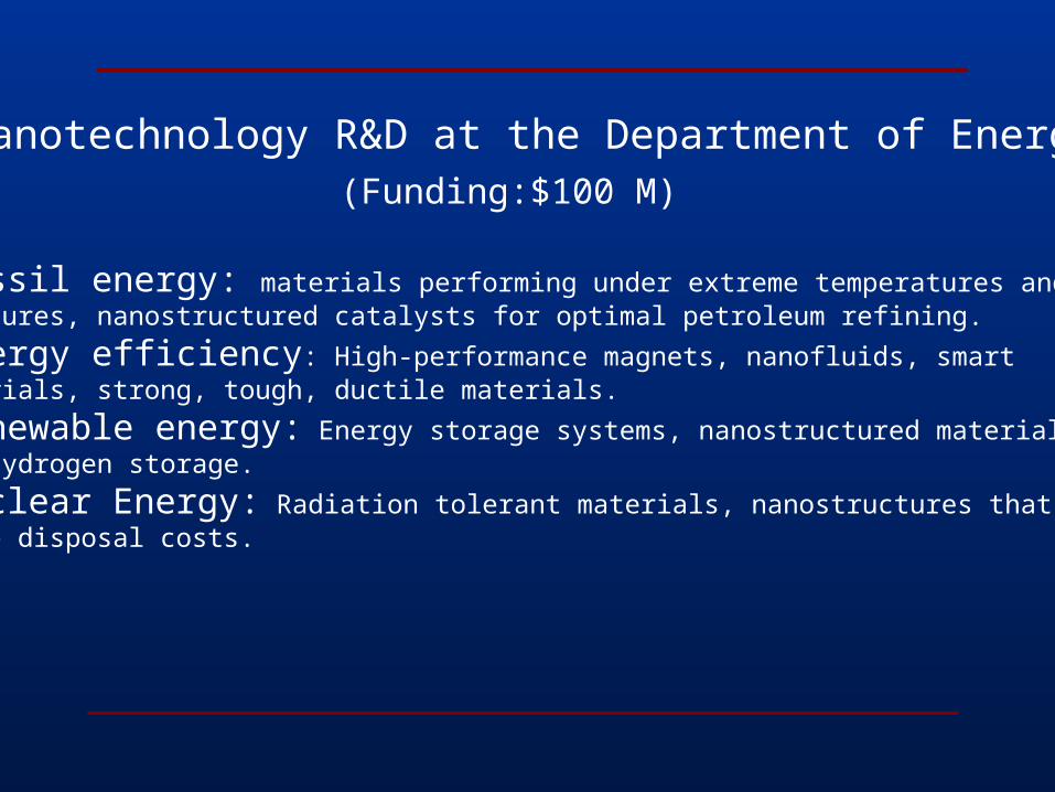
Nanotechnology R&D at the Department of Energy(Funding:$100 M)
•Fossil energy: materials performing under extreme temperatures and pressures, nanostructured catalysts for optimal petroleum refining.
•Energy efficiency: High-performance magnets, nanofluids, smartMaterials, strong, tough, ductile materials.
•Renewable energy: Energy storage systems, nanostructured materialsfor hydrogen storage.
•Nuclear Energy: Radiation tolerant materials, nanostructures that lowerwaste disposal costs.

Nanotechnology R&D at NASA
(Funding:$46 M)
•Nanostructured Materials: High strength/mass ratio, smart materials,
•Nanoelectronics: Space qualified data storage, self-healing systems forextended missions.
•Sensors: Nanodevices, NEMS flight system.
•Nanoscience: Self-assembly and processing in space, space-inducedhealth effects.
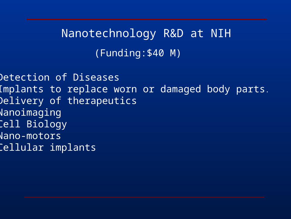
Nanotechnology R&D at NIH
(Funding:$40 M)
•Detection of Diseases•Implants to replace worn or damaged body parts.
•Delivery of therapeutics•Nanoimaging•Cell Biology•Nano-motors•Cellular implants
