waves and optics - iare
TRANSCRIPT

1
LECTURENOTES
ON
WAVES AND OPTICS
IB.Tech I semester
Dr.Koteswararao.P Associate. Professor
FRESHMAN ENGINEERING
INSTITUTE OF AERONAUTICAL ENGINEERING (Autonomous) Dundigal, Hyderabad - 500 043

2
NDEX
Module Contents Page
I QUANTUM MECHANICS 1-18
II INTRODUCTION TO SOLIDS AND
SEMICONDUCTORS 19-40
III LASERS AND FIBER OPTICS 41-57
IV LIGHT AND OPTICS 58 –83
V HARMONIC OSCILLATIONS AND WAVES IN ONE DIMENSION
83 - 98

3
UNIT-I
PRINCIPLES OF QUANTUM MECHANICS
Introduction
At the end of nineteenth century, physicists had every reason to regard the Newtonian
laws governing the motion of material bodies and Maxwell‟s laws of electromagnetism, as
fundamental laws of physics. They believed that there should be some limitation on the validity
of these laws which constitute classical mechanics. To understand the submicroscopic world of
the atom and its constituents, it become necessary to introduce new ideas and concepts which led
to which led to the mathematical formulation of quantum mechanics. That had an immediate and
spectacular success in the explanation of the experimental observations.
Quantum mechanics is the science of the submicroscopic. It explains the behavior of
matter and its interactions with energy on the scale of atoms and its constituents.
Light behaves in some aspects like particles and in other aspects like waves. Quantum
mechanics shows that light, along with all other forms of electromagnetic radiation, comes in
discrete units, called photons, and predicts its energies, colors, and spectral intensities. A single
photon is a quantum, or smallest observable amount, of the electromagnetic field because a
partial photon has never been observed.
Considering the above facts, it appears difficult to accept the conflicting ideas that
radiation has a dual nature, i.e., radiation is a wave which is spread out over space and also a
particle which is localized at a point in space. However, this acceptance is essential because
radiation sometimes behaves as a wave and at other times as a particle as explained below:
(1) Radiations including visible light, infra-red, ultraviolet, X-rays, etc. behave as waves in
experiments based on interference, diffraction, etc. This is due to the fact that these phenomena
require the presence of two waves at the same position at the same time. Obviously, it is difficult
for the two particles to occupy the same position at the same time. Thus, we conclude that
radiations behave like wave..
(2) Planck‟s quantum theory was successful in explaining black body radiation, the photo
electric effect, the Compton Effect, etc. and had clearly established that the radiant energy, in its
interaction with matter, behaves as though it consists of corpuscles. Here radiation interacts with
matter in the form of photon or quanta. Thus, we conclude that radiations behave like particle.
Black body radiation A body that completely absorbs all waves lengths of radiation incident on it at low
temperatures or emits different wave lengths of radiation at higher temperatures is known as a
black body.

4
Figure 1 Black body
An approximate realization of a black surface is a hole in the wall of a large enclosure.
Any light entering the hole is reflected within the internal surface of the body indefinitely or
absorbed within the body and is unlikely to re-emerge, making the hole a nearly perfect absorber.
The radiation confined in such an enclosure may or may not be in thermal equilibrium,
depending upon the nature of the walls and the other contents of the enclosure.
Figure 2 Black body radiation distribution
Plank’s law
Plank assumed that the walls of the black body consist of largre number of electrical
oscillators, vibrating with their own natural frequencies. An oscillator possesses an energy equal
to hu. Where h is Planks constant and v is the frequency of oscillator.
An oscillator may lose or gain energy by emitting or by absorbing photons respectively.
Plank derived an equation for the energy per unit volume of black body in the entire spectrum of
black body radiation. The spectral radiance of a body, Bν, describes the amount of energy it gives

5
off as radiation of different frequencies. It is measured in terms of the power emitted per unit
area of the body, per unit solid angle that the radiation is measured over, per unit frequency.
Planck showed that the spectral radiance of a body for frequency ν at absolute temperature T is
given by
E(λ, T) =2𝑐2
𝜆5∗
1
𝑒𝑥𝑝 𝑐
𝜆𝐾 𝑇 −1
---------------------(1)
Where kis the Boltzmann constant, h is the Planck constant, and c is the speed of light in
the medium, whether material or vacuum. The spectral radiance can also be expressed per unit
wavelength λ instead of per unit frequency.
Photoelectric effect
Figure 3 Photoelectric effect
The photoelectric effect is the emission of electrons or other free carriers when light
shines on a material. Electrons emitted in this manner can be called photo electrons. This
phenomenon is commonly studied in electronic physics, as well as in fields of chemistry, such as
quantum chemistry or electrochemistry.

6
Figure 4 Black diagram of Photo electric effect
Einstein assumed that a photon would penetrate the material and transfer its energy to an
electron. As the electron moved through the metal at high speed and finally emerged from the
material, its kinetic energy would diminish by an amount ϕ called the work function (similar to
the electronic work function), which represents the energy required for the electron to escape the
metal. By conservation of energy, this reasoning led Einstein to the photoelectric equation Ek =
hf − ϕ, where Ek is the maximum kinetic energy of the ejected electron.
Compton Effect The scattering of a photon by a charged particle like an electron. It results in a decrease in
energy of the photon called the Compton Effect. Part of the energy of the photon is transferred to
the recoiling electron.
The interaction between an electron and a photon results in the electron being given part
of the energy (making it recoil), and a photon of the remaining energy being emitted in a
different direction from the original, so that the overall momentum of the system is also
conserved. If the scattered photon still has enough energy, the process may be repeated. In this
scenario, the electron is treated as free or loosely bound.
Compton derived the mathematical relationship between the shift in wavelength and the
scattering angle of the X-rays by assuming that each scattered X-ray photon interacted with only
one electron. His paper concludes by reporting on experiments which verified his derived
relation:
(𝜆1 − 𝜆) =
𝑚𝑜𝑐(1 − cos Ɵ)------------(2)

7
Figure 5 Compton Effect
de- Broglie Hypothesis
In quantum mechanics, matter is believed to behave both like a particle and a wave at the
sub-microscopic level. The particle behavior of matter is obvious. When you look at a table, you
think of it like a solid, stationary piece of matter with a fixed location. At this macroscopic scale,
this holds true. But when we zoom into the subatomic level, things begin to get more
complicated, and matter doesn't always exhibit the particle behavior that we expect.
This non-particle behavior of matter was first proposed in 1923, by Louis de Broglie, a
French physicist. In his PhD thesis, he proposed that particles also have wave-like properties.
Although he did not have the ability to test this hypothesis at the time, he derived an equation to
prove it using Einstein's famous mass-energy relation and the Planck equation. These waves
associated with particles are named de- Broglie waves or matter waves.
Expression for de- Broglie wavelength
The expression of the wavelength associated with a material particle can be derived on the
analogy of radiation as follows:
Considering the plank‟s theory of radiation, the energy of photon (quantum) is
E = h𝜐 = 𝑐
𝜆 → (3)
Where c is the velocity of light in vacuum and 𝜆 is its wave length.

8
According to Einstein energy – mass relation
E = mc2 → (4)
𝜆 =
𝑚𝑐 =
𝑝 → (5)
Where mc = p is momentum associated with photon.
If we consider the case of material particle of mass m and moving with a velocity v , i.e
momentum mv, then the wave length associated with this particle ( in analogy to wave length
associated with photon ) is given by
𝜆 =
𝑚𝑣 =
𝑝 → (6)
Different expressions for de-Broglie wavelength
(a) If E is the kinetic energy of the material particle then
E = 1
2 mv
2 =
1
2
𝑚2𝑣2
𝑚 =
𝑝2
2𝑚
⟹ p2 = 2mE or p = 2𝑚𝐸
Therefore de- Broglie wave length 𝜆 =
2𝑚𝐸 → (7)
(b) When a charged particle carrying a charge „q‟ is accelerated by potential difference v, then
its kinetic energy K .E is given by
E = qV
Hence the de-Broglie wavelength associated with this particle is
𝜆 =
2𝑚𝑞𝑉 → (8)
For an electron q = 1.602×10⁻¹⁹
Mass m = 9.1 X 10⁻³¹
kg
∴ 𝜆 = 6.626 × 10⁻³⁴
2 × 9.1 × 10−31 × 1.602 × 10−19𝑉
= 150
𝑉 =
12.26
𝑉 A
0 → (9)
Properties of Matter Waves
Following are the properties of matter waves:
(a) Lighter is the particle, greater is the wavelength associated with it.
(b) Smaller is the velocity of the particle, greater is the wavelength associated with it.
(c) When v = 0, then 𝜆 = ∞ , i.e. wave becomes indeterminate and if v = ∞ then
𝜆 = 0. This shows that matter waves are generated only when material particles are in
motion.
(d) Matter waves are produced whether the particles are charged particles or not
(𝜆 =
𝑚𝑣 is independent of charge). i.e., matter waves are not electromagnetic waves but
they are a new kind of waves .

9
(e) It can be shown that the matter waves can travel faster than light i.e. the velocity of
matter waves can be greater than the velocity of light.
(f) No single phenomenon exhibits both particle nature and wave nature simultaneously.
Distinction between matter waves and electromagnetic waves
S.No Matter Waves Electromagnetic Waves 1
2
3
4.
5.
Matter waves are associated with moving
particles (charged or uncharged)
Wavelength depends on the mass of the
particle and its velocity,
𝜆 =
𝑚𝑣
Matter waves can travel with a velocity
greater than the velocity of light.
Matter wave is not electromagnetic wave.
Matter wave require medium for
propagation, i.e, they cannot travel through
vacuum.
Electromagnetic waves are produced only by
accelerated charged particles.
Wavelength depends on the energy of photon
Travel with velocity of light
c= 3×10⁸ m/s
Electric field and magnetic field oscillate
perpendicular to each other.
Electromagnetic waves do not require any
medium for propagation, i.e., they can pass
through vacuum.
Davisson and Germer’s Experiment
The first experimental evidence of matter waves was given by two American physicists,
Davisson and Germer in 1927. The experimental arrangement is shown in figure 3.1(a).
The apparatus consists of an electron gun G where the electrons are produced. When the
filament of electron gun is heated to dull red electrons are emitted due to thermionic emissions.
Now, the electrons are accelerated in the electric field of known potential difference. These
electrons are collimated by suitable slits to obtain a fine beam which is then directed to fall on a
large single crystal of nickel, known as target T which is rotated about an angle along the
direction of the beam is detected by an electron detector (Faraday cylinder) which is connected
to a galvanometer. The Faraday cylinder „c‟ can move on a circular graduated scale s between
290c to 90
0c to receive the scattered electrons.

10
Figure 6Davisson and Germer’s experimental arrangement for verification of matter waves
First of all, the accelerating potential V is given a low value and the crystal is set at any
orbital azimuth (θ). Now the Faraday cylinder is moved to various positions on the scale‟s‟ and
galvanometer current is measured for each position. A graph is plotted between galvanometer
current against angle θ between incident beam and beam entering the cylinder [Figure3.1(b)].
The observations are repeated for different acceleration potentials.
Figure 7Variation of Galvanometer current with variation of angle θ between incident beam and beam
entering the cylinder
It is observed that a „bump‟ begins to appear in the curve for 44 volts. Following points are
observed.
(a) With increasing potential, the bump moves upwards.
(b) The bump becomes most prominent in the curve for 54 volts at θ = 500.
(c) At higher potentials, the bumps gradually disappear.

11
The bump in its most prominent state verifies the existence of electron waves. According to
de- Broglie, the wavelength associated with electron accelerated through a potential V is given
by
𝜆 = 12.26
𝑉 A
0.
Hence, the wavelength associated with an electron accelerated through 54 volt is
𝜆 = 12.26
54 = 1.67 A
0
From X-ray analysis, it is known that a nickel crystal acts as a plane diffraction grating
with space d = 0.91 A0 [see Figure 3.1(c)]. According to experiment, we have diffracted electron
beam at θ = 500. The corresponding angle of incidence relative to the family of Bragg plane
θ1 =
180−50
54 = 65
0
Using Bragg‟s equation (taking n=1), we have
𝜆 = 2dsinθ
= 2(0.91A0) sin 650
This is in good agreement with the wavelength computed from de-Broglie hypothesis.
Figure 8 Bragg planes in Nickel crystal
As the two values are in good agreement, hence, confirms the de-Broglie concept of
matter waves.
Schrodinger's time independent wave equation
Schrodinger developed a differential equation whose solutions yield the possible wave
functions that can be associated with a particle in a given situation. This equation is popularly
known as Schrodinger equation. The equation tells us how the wave function changes as a result
of forces acting on the particle. One of its forms can be derived by simply incorporating the de-
Broglie wavelength expression into the classical wave equation.
If a particle of mass „m‟ moving with velocity v is associated with a group of waves, let
𝜓 be the wave function of the particle. Also let us consider a simple form of progressing wave
represented by the equation
𝜓 = 𝜓0sin(𝜔t − kx) ------------(1)

12
Where 𝜓 = 𝜓 (x, t)
𝜓0 is amplitude
Differentiating eq (1) partially with respect to „x‟, we get 𝜕𝜓
𝜕𝑥 = -K 𝜓0cos(𝜔t − kx)
Again differentiating equation (1) with respect to „x‟
𝜕2𝜓
𝜕𝑥2 = −K
2 𝜓0 sin (𝜔t-kx)
𝜕2𝜓
𝜕𝑥2 = −k2𝜓
𝜕2𝜓
𝜕𝑥2 + k2𝜓 = 0 ----------------------------------------- (2)
Since k = 2𝜋
𝜆 ,
𝜕2𝜓
𝜕𝑥2 +
4𝜋2
𝜆2𝜓 = 0 ---------------------------(3)
Eq (2) or Eq (3) is the differential form of the classical wave equation. Now, incorporating de-
Broglie wavelength expression 𝜆 =
𝑚𝑣 in to eq (3), we get
𝜕2𝜓
𝜕𝑥2 +4𝜋2𝑚2𝑣2
2 𝜓 = 0 → (4)
The total energy E of the particle is the sum of its kinetic energy k and potential energy V
i.e., E = K + V
But K = 1
2 mv
2
∴ E = 1
2 mv
2 + V
1
2 mv
2 = E – V
m2v
2 = 2m (E - V) → (5)
Substituting eq (5) in eq (4), we get
𝜕2𝜓
𝜕𝑥2 +8𝜋2m(E − V)
2 𝜓 = 0 → (6)
In quantum mechanics, the value
2𝜋 occurs most frequently. Hence we denote ђ =
2𝜋
using this notation, we have
𝜕2𝜓
𝜕𝑥2 + 2m(E − V)
ђ2 𝜓 = 0 → (7)
For simplicity, we have considered only one dimensional wave extending eq(7) for a
3 – dimensional wave
𝜕2𝜓
𝜕𝑥2 +
𝜕2𝜓
𝜕𝑦2 +
𝜕2𝜓
𝜕𝑧2 +
2m(E − V)
ђ2𝜓 = 0 → (8)
Where 𝜓 (x, y, z); here, we have considered only stationary states of 𝜓after separating the
time dependence of 𝜓
The Laplacian operator is defined as
∇2 =
𝜕2
𝜕𝑥2 + 𝜕2
𝜕𝑦2 + 𝜕2
𝜕𝑧2 → (9)
Hence eq (10) can be written as
∇2𝜓 + 2m(E − V)
ђ2 𝜓 = 0 → (10)
13
This is Schrodinger wave equation. Since time factor doesn‟t appear, eq(8) or eq(10) is called
„time independent Schrodinger wave equation‟ in three dimensions.
Physical significance of wave function 𝝍
(1) The wave function 𝜓has no direct physical meaning. It is a complex quantity representing
the variation of matter wave.
(2) It connects the practical nature and its associated wave nature statically.
(3) | 𝜓 |2 (or 𝜓𝜓 * if function is complex) at a point is proportional to the probability of
finding the particle at that point at any given time. The probability density at any point is
represented by | 𝜓|2.
(4) If the particle is present in a volume dxdydz, then | 𝜓 |2dxdydz =1
If a particle is present somewhere in space
𝜓2 dx dy dz = 1
∞
−∞
Or 𝜓𝜓 ∗ dx dy dz = 1
∞
−∞
The wave function satisfying the above condition is said to be normalized.
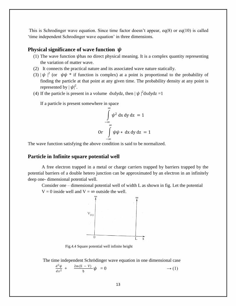
Particle in Infinite square potential well
A free electron trapped in a metal or charge carriers trapped by barriers trapped by the
potential barriers of a double hetero junction can be approximated by an electron in an infinitely
deep one- dimensional potential well.
Consider one – dimensional potential well of width L as shown in fig. Let the potential
V = 0 inside well and V = ∞ outside the well.
Fig.4.4 Square potential well infinite height
The time independent Schrödinger wave equation in one dimensional case
𝑑2𝜓
𝑑𝑥2 +
2m(E − V)
ђ 𝜓 = 0 → (1)

14
For a particle present inside the well where V=0 and 𝜓 = 𝜓(𝑥)
𝑑2𝜓
𝑑𝑥2 + 2mE
ђ2 𝜓 = 0 → (2)
Let the general solution of eq (2) be
𝜓(𝑥) = A sin 𝑘𝑥 + B sin 𝑘𝑥 → (3)
Where A and B are constants which can be determined from boundary conditions
𝜓(𝑥) = 0 at x = 0
And 𝜓(𝑥) = 0 at x = L → (4)
Since 𝜓(𝑥) = 0 at x = 0
0= A sin 𝑘(0) + B cos 𝑘(0)
⟹ B = 0 → (5)
Since 𝜓(𝑥) = 0 at x = L
0 = A sin 𝑘𝐿
Which means A =0 or sin 𝑘𝐿 = 0 since both A and B cannot be zero, A≠ 0. If
A = 0, then 𝜓 = 0 everywhere. This means that the particle is not in the well. The only
meaningful way to satisfy the condition is
sin 𝑘𝐿 = 0,
or kL = nπ ; n = 1,2,3,…
∴ k = nπ
𝐿 → (6)
Thus, eq (3) simplifies to
𝜓(𝑥) = A sin nπ
𝐿x → (7)
Differentiating 𝜓 in eq (7)
𝑑𝜓
𝑑𝑥= A
nπ
𝐿cos
nπ
𝐿 x
Again Differentiating, we get
𝑑2𝜓
𝑑𝑥2= − A
n2π2
𝐿2 sin nπ
𝐿 x
𝑑2𝜓
𝑑𝑥2 = −
n2π2
𝐿2𝜓 = 0
𝑑2𝜓
𝑑𝑥2 +
n2π2
𝐿2 𝜓 = 0 → (8)
Comparing eq (2) and eq (8), we get
2mE
ђ2 =
n2π2
𝐿2 = k
2
E = n2 π2 ђ2
2𝑚𝐿2
n is called the quantum number. Thus we obtain an important result. The particle cannot possess
any value of energy as assumed in classical case, but it possesses only discrete set of energy
values.
The energy of the nth
quantum level,

15
En = n2 π2 ђ2
2𝑚𝐿2 =
n2 h2
8𝑚𝐿2 (since ђ =
2𝜋 ) → (9)
The wave functions and the corresponding energy levels of the particles are as suggested in
Figure 3.5
Fig.4.5 Ground state and first two excited states of an electron in a potential well: a) the electron wave functions and
b) the corresponding probability density functions. The energies of these three states are shown on the right.
We are still left with an arbitrary constant „A‟ in eq (7). It can be obtained by applying
normalization condition i.e.; the probability of finding the particle inside the box is unity.
𝜓 𝑥 2 𝑑𝑥 = 1
𝐿
0
𝐴2𝑠𝑖𝑛2 𝑛𝜋𝑥
𝐿𝑑𝑥
𝐿
0 = 1
A2
1
2
𝐿
0 1 − 𝑐𝑜𝑠
2𝑛𝜋
𝑙𝑥 𝑑𝑥 = 1
𝐴2
2 [x −
𝐿
2𝜋𝑛 𝑠𝑖𝑛
2𝜋𝑛𝑥
𝐿 ]
L 0 = 1
⟹ 𝐴2
2 𝐿 − 0 − 0 − 0 = 1
𝐴2𝐿
2 = 1 or A =
2
𝐿 → 10)
∴The normalized wave function is
𝜓n = 2
𝐿 sin
𝑛𝜋𝑥
𝐿 → (11)
Notice that the number of nodes (places where the particle has zero probability of being located)
increases with increasing energy n. Also note that as the

16
energy of the particle becomes greater, the quantum mechanical model breaks down as the
energy levels get closer together and overlap, forming a continuum.
This continuum means the particle is free and can have any energy value. At such high energies,
the classical mechanical model is applied as the particle behavesmore like a continuous wave.
Therefore, the particle in a box problem is an example of Wave-Particle Duality.

17
UNIT-II
INTRODUCTION TO SOLIDS AND SEMICONDUCTORS
Bloch′s theorem
Crystalline solid consists of a lattice which is composed of a large number of ionic cores
at regular intervals and the conduction electrons move throughout the lattice.
Let us consider the picture of the lattice in only one dimension, i.e., only an array of ionic
cores along x-axis. If we plot the potential energy of a conduction electron as a position in the
lattice, the variation of potential energy is as shown in figure. The potential is minimum at the
positive ion sites and maximum between the two ions.
periodic positive ion cores inside metallic crystals. b) One dimensional periodic potential in crystal.
The one dimension Schrodinger equation corresponding to this can be written as 𝑑²𝜓
𝑑𝑥² +
8𝜋²𝑚
²[E-V(x)] ψ = 0 → (1)
The periodic potential V(x) may be defined by means of the lattice constant „a‟ as
V(x) = V(x+a) → (2)
Bloch considered the solution as
ψK (x) =𝑒𝑥𝑝(ikx)Uk(x) → (3)
Eqn (2) is known as Bloch function. Uk (x) is periodic with the periodicity of the crystal
lattice. The free electron wave is modulated by periodic function Uĸ(x) is periodic with the
periodicity of the crystal lattice. The free electron wave is modulated by periodic function U k(x).
For a linear chain of atoms of length „L‟ in one dimensional case with „N‟ (= even) number of
atoms in the chain,
Uĸ(x) = Uĸ (x+Na) → (4)
From eqn (3) and eqn (4)
Ψĸ(x +na) = Uĸ(x+Na) 𝑒[𝑖𝑘(𝑥+𝑁𝑎]
= 𝑒(𝑖𝑘𝑁𝑎 ) Uĸ(x) 𝑒(𝑖𝑘𝑥 )
= ψĸ(x) 𝑒(𝑖𝑘𝑁𝑎 ) → (5)
This is referred to as Bloch condition.

18
Now,
ψĸ(x+Na)ψĸ*(x+Na) = ψĸ(x)𝑒(ikNa).ψĸ*(x) e
(-ikNa)
= ψĸ(x) ψĸ*(x) e(0)
Ψĸ(x+Na) Ψĸ*(x+na) = Ψĸ(x) Ψĸ*(x) → (6)
This means that the electron is not located around any particular atom and the probability of
finding the electron is same throughout the crystal.
The Kronig-Penny Model The periodic potential assumed by Kronig and Penny is shown in Figure. i.e., a series of
rectangular wells of width „a‟ and are placed at a separation of b. in the regions where 0<x<a, the
potential energy is zero and in regions such as –b < x < 0, the potential energy is V₀.
One dimensional periodic potential assumed by Kronig and Penny
The main features of the model and its predictions can be explained qualitatively
Main features of the model A. Schrodinger equation: The dynamical behavior of electrons in the Kronig-Penny model is represented by the following
Schrodinger equation, 𝑑²𝜓
𝑑𝑥 ²+[
2𝑚
²] Eψ=0 for 0 < x < a
And 𝑑2𝜓
𝑑𝑥2+ [
2𝑚
2] 𝐸 − 𝑉0 𝜓 = 0 𝑓𝑜𝑟 − 𝑏 < 𝑥 < 0 → (1)
Let us assume that total energy „E‟ of the electron under consideration is less than V₀.
Further, let us substitute α²=2𝑚𝐸
² and β² =
2𝑚
²(V₀-E) → (2)
Where α and β are real quantities.
Now Eq(1) becomes 𝑑²𝜓
𝑑𝑥 ²+ α²ψ=0, for 0<x<a
And 𝑑²𝜓
𝑑𝑥 ²– β²ψ=0, for –b < x < 0 → (3)
These equations can be solved with the help of block theorem. The final solution of eq (3) is
given in the form of the following condition.

19
P𝑠𝑖𝑛𝛼𝑎
𝛼𝑎+ cosαa =coska → (4)
Where P =𝑚𝑏
²V₀a is scattering power of the potential barrier and V₀ is barrier strength. That
means, eq (3) will have a solution only when the condition (4) is satisfied.
Graph of αa versus 𝑷𝒔𝒊𝒏𝜶𝒂
𝜶𝒂 + cosαa
For the best understanding of the meaning of eq(4), let us consider the plot of the
condition(4) i.e. L.H.S versus αa. Since the values of coska on R.H.s of eq (4) lie between +1 and
-1, αa (which is a measure of energy) can take only those values for which the total left hand side
(L.H.S) value lies between -1 and +1. Other values are not allowed. This means that energy E is
restricted to lie within certain ranges which form the allowed energy bands or zones.
Plot of the left hand side of eq (4) as a function of αa for p =
3𝜋
2. The solid and broken lines on the abscissa (αa- axis)
correspond to allowed and forbidden energy regions of the energy spectrum respectively that are plotted in fig.
Conclusions of the graph 1. The energy spectrum consists of alternative regions of allowed and vacant bands.
Forbidden band implies that the energy levels that lie in this region are not occupied by
the electrons.
2. The allowed (shaded) bands are narrowest for low values of energy and become broader
as energy increases, the unallowed (forbidden) bands becoming narrower.
3. a) For P=0 (i.e. on the extreme left), the whole energy spectrum is quasi-continuous. That
is all allowed bands are joined together forming an almost continuum.
b) However, the width of a particular allowed band decreases with increase in the value
of P. As P→ ∞, the allowed energy bands compress into simple energy levels and thus
result in a line spectrum.
Origin of Energy band formation in solids In an isolated atom, the electrons are tightly bound and have discrete, sharp energy levels
[Figure]. When two identical atoms are brought closer, the outermost orbits of these atoms
overlap and interact.
When the wave functions of the electrons of the different atoms begin to overlap considerably,
the energy levels split into two

20
. Splitting of energy levels due to interatomic interaction
If more atoms are bought together, more levels are formed and for a solid of N atoms, each of the
energy levels of an atom splits into N levels of energy [Figure].
The levels are so close together that they form an almost continuous band. The width of
this band depends on the degree of overlap of the electrons of adjacent atoms and is largest for
the outermost atomic electrons.
In a solid, many atoms are brought together that the split energy levels form a set of
energy bands of very closely spaced levels with forbidden energy gaps between them.
Overlapping of these atoms occurs for smaller equilibrium spacing ro.
. With decrease of interatomic spacing overlapping of energy bands take place
The band corresponding to outermost orbit is called conduction band and the next band is called
valence band. The gap between these two allowed bands is called forbidden energy gap or band
gap. According to the width of the gap between the bands and band occupation by electrons all
solids can be classified broadly into three groups namely, conductors, semiconductors and
insulators
Classification of materials into conductors, semiconductors and insulators
On the basis of band theory, solids can be broadly classified into three categories, viz, insulators,
semiconductors and conductors. Their band structures can be as shown in figure.

21
Insulators
1. In case of insulators, the forbidden gap is very wide. Due to this fact electrons cannot jump
from valence band to conduction band.
2. They have completely filled valence band and completely empty conduction band.
3. The resistivity of insulators is very high.
4. Insulators are bad conductors of electricity.
.Valence and conduction bands of insulator separated by large band gap
Semiconductors 1. In semiconductors, the band gap is very small (0.7 eV for germanium and 1.1 eV for silicon).
2. At 0k, these are no electrons in the conduction band and the valence band is completely filled.
As the temperature increases, electrons from the valence band jump into conduction band
3. . 3. The resistivity varies from 10 -14 to 107Ω meter.
4. They have electrical properties between those of insulators and conductors.

22
. Valence and conduction bands of semiconductor separated by small band gap
Conductors 1. In case of conductors, there is no forbidden gap and the valence band conduction band
overlaps each other.
2. Plenty of free electrons are available for electrical conduction.
3. They posses very low resistivity and very high conductivity values.
4. Metals c like copper, iron etc. are best examples of conductors.
. Metals having (a) partially filled valence band and (b) overlap of completely filled valence band

23
Intrinsic Semiconductor Pure germanium or silicon called an intrinsic semiconductor. Each atom possesses four valence
electrons in outer most orbits. At T = 0K a 2-D representation of the crystal of silicon & band
diagram is shown in the figure .
Intrinsic silicon crystal at T =0K (a) 2-D representation of silicon crystal
(c) Energy band diagram of intrinsic semiconductor
Explanation: At 0K, all the valence electrons of silicon atoms are in covalent bonds and their
energies constitute a band of energies called valance band (VB). So at 0K, VB is completely
filled & conduction band (CB) is empty.
If we rise temperature (T>0K), some of the electrons which are in covalent bonds break
the bonds become free and move from VB to CB. The energy required should be greater than the
energy gap of a semiconductor (E>Eg). The electron vacancy or deficiency created in VB is
called holes. This is shown in the figure 3 below.
Silicon crystal at temperature above 0K (a) Due to thermal energy breaking of
Covalent bonds take place (b) Energy band representation

24
Electron concentration in intrinsic semiconductor in conduction band (n) Definition: The no. of free electrons per unit volume of the conduction band of a given intrinsic
semiconductor is called electron concentration, represented by „n‟.
(a) Energy band diagram of silicon at T = 0K
(b) Energy band diagram of silicon at T > 0K
Derivation: Let the no. of free electrons per unit volume of the semiconductor having energies E
and E + dE in CB is represented by n (E) dE. It is obtained by multiplying the density of energy
states ZC (E) d (E). [No. of energy states per unit volume] and Fermi – Dirac distribution
function for the Probability of occupation of electrons FC (E)
Therefore n (E) dE = [ZC (E) d (E)] [FC (E)] → (1)
Where Z v (E) d (E) = Density of energy states
F h (E) = Probability of occupation of electrons given by Fermi – Dirac function
The total no. of electrons in CB per unit volume between the energies EC to E ct is given by
integrating equation (1) with limits EC to E ct
n = 𝑛 𝐸 𝑑𝐸𝐸𝑐𝑡
𝐸𝐶 → (2)
But equation (2) can be written as
n = 𝑛 𝐸 𝑑𝐸∞
𝐸𝐶+ 𝑛 𝐸 𝑑𝐸
𝐸𝑐𝑡
∞ → (3)
n = 𝑛 𝐸 𝑑𝐸∞
𝐸𝐶− 𝑛 𝐸 𝑑𝐸
∞
𝐸𝑐𝑡 →(4)
In equation (4) the second term vanishes (disappears).
Since, above E c t electrons do not present. Hence equation (4) becomes
n = 𝑛 𝐸 𝑑𝐸∞
𝐸𝐶
n = [∞
𝐸𝑐𝑍𝐶 𝐸 𝑑𝐸] × 𝐹𝐶 𝐸 →(5)
Since from equation (1)
But 𝐹𝐶 𝐸 is Fermi – Dirac distribution function;
𝐹𝐶 𝐸 =1
1+𝑒
𝐸−𝐸𝐹𝐾𝐵𝑇
→(6)
Here E > EF, 𝑖. 𝑒. 𝑒𝐸−𝐸𝐹𝐾𝐵𝑇 >> 1

25
Hence „1‟ can be neglected in equation (6)
𝐹𝐶 𝐸 =1
𝑒𝐸−𝐸𝐹𝐾𝐵𝑇
𝐹𝐶 𝐸 = 𝑒𝐸𝐹−𝐸
𝐾𝐵𝑇 → (7)
Also the density of electrons
ZC (E) d (E) = 𝜋
2[
8𝑚𝑒∗
2]
3
2 (𝐸)1
2 dE → (8)
Here E > EC .Since EC is the minimum energy state in CB. Hence equation (8) becomes
ZC (E) d (E) = 𝜋
2[
8𝑚𝑒∗
2 ]3
2 (𝐸 − 𝐸𝐶)1
2 dE → (9)
Substituting equations (7) & (9) in equation (5) we get
n = 𝜋
2[
8𝑚𝑒∗
2]
3
2 (𝐸 − 𝐸𝐶)1
2∞
𝐸𝐶𝑒
𝐸𝐹−𝐸
𝐾𝐵𝑇 dE
n = 𝜋
2[
8𝑚𝑒∗
2 ]3
2 (𝐸 − 𝐸𝐶)1
2∞
𝐸𝐶𝑒
𝐸𝐹−𝐸
𝐾𝐵𝑇 dE → (10)
Let 휀 = 𝐸 − 𝐸𝐶
d휀 = 𝑑𝐸 𝐸𝐶is constant . The limits are 휀 = 0 to 휀= ∞
Hence equation (10) can be written as
n = 𝜋
2[
8𝑚𝑒∗
2 ]3
2 (휀)1
2∞
휀=0𝑒
𝐸𝐹− 휀+𝐸𝐶
𝐾𝐵𝑇 𝑑휀
n = 𝜋
2[
8𝑚𝑒∗
2 ]3
2 𝑒(𝐸𝐹−𝐸𝐶)
𝐾𝐵𝑇 (휀)1
2∞
휀=0𝑒
−휀
𝐾𝐵𝑇𝑑휀 → (11)
In equation (11) But (휀)1
2∞
휀=0𝑒
−휀
𝐾𝐵𝑇𝑑휀 = 𝜋
2(𝑘𝐵𝑇)
3
2 → (12)
Substituting (12) in (11) we get
n = 𝜋
2[
8𝑚𝑒∗
2 ]3
2 𝑒(𝐸𝐹−𝐸𝐶)
𝐾𝐵𝑇 𝜋
2(𝑘𝐵𝑇)
3
2
n = 1
4[
8𝜋𝑚 𝑒∗𝐾𝐵𝑇
2 ]3
2 𝑒(𝐸𝐹−𝐸𝐶)
𝐾𝐵𝑇
n = 8
4[
2𝜋𝑚 𝑒∗𝐾𝐵𝑇
2 ]3
2 𝑒(𝐸𝐹−𝐸𝐶)
𝐾𝐵𝑇
n = 2[2𝜋𝑚 𝑒
∗𝐾𝐵𝑇
2]
3
2 𝑒−(𝐸𝐶−𝐸𝐹)
𝐾𝐵𝑇 → (13)
Here NC =2[2𝜋𝑚 𝑒
∗𝐾𝐵𝑇
2 ]3
2 Therefore n = 𝑁𝐶𝑒−(𝐸𝐶−𝐸𝐹 )
𝐾𝐵𝑇
Hole concentration in the valance band of intrinsic semiconductor(p)
Definition: The number of holes per unit volume of the valance band of a given intrinsic
semiconductor is called hole concentration, represented by „p‟.
Derivation: Let the number of holes per unit volume of the semiconductor having energies E, E
+ dE in VB is represented by p (E) dE. It is obtained by multiplying the density of energy states
ZV (E) d (E) [No. of energy states per unit volume] and Fermi – Dirac distribution function for
the Probability of occupation of holes F h (E).

26
(a) Energy band diagram of silicon at T = 0K
(b) Energy band diagram of silicon at T > 0K
Therefore p (E) dE = [Z v (E) d (E)] [F h (E)] → (1)
Where Z v (E) d (E) = Density of energy states.
F h (E) = Hole probability given by Fermi – Dirac function
The total no. of holes in VB per unit volume between the energies E v b to E v is given by
integrating equation (1) with limits E v b to E v
p = 𝑝 𝐸 𝑑𝐸𝐸𝑣
𝐸𝑣𝑏 →(2)
But equation (2) can be written as
p = 𝑝 𝐸 𝑑𝐸−∞
𝐸𝑣𝑏+ 𝑝 𝐸 𝑑𝐸
𝐸𝑣
−∞ → (3)
p = − 𝑝 𝐸 𝑑𝐸𝐸𝑣𝑏
−∞+ 𝑝 𝐸 𝑑𝐸
𝐸𝑣
−∞→ (4)
In equation (4) the first term vanishes (disappears).
Since, below E v b holes do not present. Hence equation (4) becomes
p = 𝑝 𝐸 𝑑𝐸𝐸𝑣
−∞
p = Zv E dE × Fh(E)𝐸𝑣
−∞→ (5)
Since from equation (1)
But 𝐹 𝐸 is Fermi – Dirac distribution function;

27
𝐹 𝐸 = 1 − 𝐹𝐶 𝐸 →(6)
= 1 −1
1+𝑒
𝐸−𝐸𝐹𝐾𝐵𝑇
Simplifying; 𝐹 𝐸 = 𝑒
𝐸−𝐸𝐹𝐾𝐵𝑇
1+𝑒
𝐸−𝐸𝐹𝐾𝐵𝑇
Divide by 𝑒𝐸−𝐸𝐹𝐾𝐵𝑇 we get
𝐹 𝐸 = 1
1+1
𝑒
𝐸−𝐸𝐹𝐾𝐵𝑇
𝐹 𝐸 = 1
1+𝑒
𝐸𝐹−𝐸𝐾𝐵𝑇
→ (6)
Here EF > E, 𝑖. 𝑒. 𝑒𝐸𝐹−𝐸
𝐾𝐵𝑇 >> 1
Hence „1‟ can be neglected in equation (6)
𝐹 𝐸 =1
𝑒𝐸𝐹−𝐸
𝐾𝐵𝑇
𝐹 𝐸 = 𝑒𝐸−𝐸𝐹𝐾𝐵𝑇 → (7)
Also the density of holes
Z v (E) d (E) = 𝜋
2[
8𝑚𝑝∗
2 ]3
2 (𝐸)1
2 dE → (8)
Here E < E v .Since E v is the maximum energy state in VB. Hence equation (8) becomes
Z v (E) d (E) = 𝜋
2[
8𝑚𝑝∗
2 ]3
2 (𝐸𝑉 − 𝐸)1
2 dE → (9)
Substituting equations (7) & (9) in equation (5) we get
p = 𝜋
2[
8𝑚𝑝∗
2 ]3
2 (𝐸𝑉 − 𝐸)1
2𝐸𝑣
−∞𝑒
𝐸−𝐸𝐹𝐾𝐵𝑇 dE
p = 𝜋
2[
8𝑚𝑝∗
2 ]3
2 (𝐸𝑉 − 𝐸)1
2𝐸𝑣
−∞𝑒
𝐸−𝐸𝐹𝐾𝐵𝑇 dE →(10)
Let 휀 = 𝐸𝑉 − 𝐸
d휀 = −𝑑𝐸 𝐸𝑉 is constant . The limits are 휀= ∞𝑡𝑜휀 = 0
Hence equation (10) can be written as
p = 𝜋
2[
8𝑚𝑝∗
2 ]3
2 (휀)1
20
휀=∞𝑒
(𝐸𝑉−휀)−𝐸𝐹𝐾𝐵𝑇 𝑑휀
p = 𝜋
2[
8𝑚𝑝∗
2 ]3
2 𝑒(𝐸𝑉−𝐸𝐹)
𝐾𝐵𝑇 (휀)1
2∞
휀=0𝑒
−휀
𝐾𝐵𝑇𝑑휀 → (11)
In equation (11) But (휀)1
2∞
휀=0𝑒
−휀
𝐾𝐵𝑇𝑑휀 = 𝜋
2(𝑘𝐵𝑇)
3
2 → (12)
Substituting (12) in (11) we get
p = 𝜋
2[
8𝑚𝑝∗
2 ]3
2 𝑒(𝐸𝑉−𝐸𝐹)
𝐾𝐵𝑇 𝜋
2(𝑘𝐵𝑇)
3
2
p = 1
4[
8𝜋𝑚 𝑝∗ 𝐾𝐵𝑇
2 ]3
2 𝑒(𝐸𝑉−𝐸𝐹)
𝐾𝐵𝑇
p = 8
4[
2𝜋𝑚 𝑝∗ 𝐾𝐵𝑇
2 ]3
2 𝑒(𝐸𝑉−𝐸𝐹)
𝐾𝐵𝑇

28
p = 2[2𝜋𝑚 𝑝
∗ 𝐾𝐵𝑇
2 ]3
2 𝑒−(𝐸𝐹−𝐸𝑉 )
𝐾𝐵𝑇 → (13)
Here NV =2[2𝜋𝑚 𝑝
∗ 𝐾𝐵𝑇
2]
3
2
p = 𝑁𝑉𝑒−(𝐸𝐹−𝐸𝑉 )
𝐾𝐵𝑇
Fermi energy level in intrinsic semiconductor At temperature T k , the electron concentration „n‟ is equal to hole concentration „p‟ in intrinsic
semiconductor.
i.e. n = p
2[2𝜋𝑚 𝑒
∗𝐾𝐵𝑇
2 ]3
2 𝑒− 𝐸𝐶−𝐸𝐹
𝐾𝐵𝑇 = 2[2𝜋𝑚 𝑝
∗ 𝐾𝐵𝑇
2 ]3
2 𝑒−(𝐸𝐹−𝐸𝑉 )
𝐾𝐵𝑇
On simplifying we get
( 𝑚𝑒∗)
3
2𝑒−(𝐸𝐶−𝐸𝐹 )
𝐾𝐵𝑇 = ( 𝑚𝑝∗ )
3
2𝑒−(𝐸𝐹−𝐸𝑉 )
𝐾𝐵𝑇
𝑒− 𝐸𝐶−𝐸𝐹
𝐾𝐵𝑇
𝑒− 𝐸𝐹−𝐸𝑉
𝐾𝐵𝑇
= ( 𝑚𝑝
∗ )3
2
( 𝑚𝑒∗)
3
2
𝑒𝐸𝐶+𝐸𝐹+𝐸𝐹−𝐸𝑉
𝐾𝐵𝑇 = [𝑚𝑝
∗
𝑚𝑒∗]
3
2
𝑒2𝐸𝐹𝐾𝐵𝑇
−(𝐸𝐶−𝐸𝑉 )
𝐾𝐵𝑇 = [𝑚𝑝
∗
𝑚𝑒∗ ]
3
2
Taking logarithms on both sides we get 2𝐸𝐹
𝐾𝐵𝑇−
(𝐸𝐶−𝐸𝑉 )
𝐾𝐵𝑇 =
3
2𝑙𝑛[
𝑚𝑝∗
𝑚𝑒∗]
2𝐸𝐹
𝐾𝐵𝑇=
(𝐸𝐶−𝐸𝑉 )
𝐾𝐵𝑇 +
3
2𝑙𝑛[
𝑚𝑝∗
𝑚𝑒∗]
𝐸𝐹 = (𝐸𝐶+𝐸𝑉 )
2 +
3
4𝐾𝐵𝑇𝑙𝑛[
𝑚𝑝∗
𝑚𝑒∗] At T > 0K
Let T = 0K 𝐸𝐹 = (𝐸𝐶+𝐸𝑉 )
2
This means EF lies in the middle between (𝐸𝐶&𝐸𝑉) of the energy gap „E g‟
As the temperature increases the electrons move from VB to CB. Also the Fermi level slightly
rises upwards towards CB. Hence 𝐸𝐹 = (𝐸𝐶+𝐸𝑉 )
2 +
3
4𝐾𝐵𝑇𝑙𝑛[
𝑚𝑝∗
𝑚𝑒∗]. It is shown in the figure 6
below.

29
(a) Fermi level 𝐸𝐹 at T = 0K (b) Upward shift of 𝐸𝐹 near EC at T> 0k
Intrinsic carrier concentration (ni) Definition: The no. of free electrons and holes per unit volume of the intrinsic semiconductor is
called intrinsic carrier concentration (n i) remains constant.
i .e. n = p = ni
n p = (ni) (ni)
𝑛𝑖2 = (n p) → (1)
𝑛𝑖 = (𝑛𝑝)1
2→ (2)
Consider equation (1) 𝑛𝑖2 = (n p)
𝑛𝑖2 = 2[
2𝜋𝑚 𝑒∗𝐾𝐵𝑇
2 ]3
2 𝑒− 𝐸𝐶−𝐸𝐹
𝐾𝐵𝑇 × 2[2𝜋𝑚 𝑝
∗ 𝐾𝐵𝑇
2 ]3
2 𝑒−(𝐸𝐹−𝐸𝑉 )
𝐾𝐵𝑇
= 4 2𝜋𝐾𝐵𝑇
2 3
(𝑚𝑒∗𝑚𝑝
∗ )3
2𝑒−𝐸𝐶+𝐸𝐹−𝐸𝐹+𝐸𝑉
𝐾𝐵𝑇
𝑛𝑖2 = 4
2𝜋𝐾𝐵𝑇
2 3
(𝑚𝑒∗𝑚𝑝
∗ )3
2𝑒−𝐸𝑔
𝐾𝐵𝑇 Since 𝐸𝐶 − 𝐸𝑉 = Eg
𝑛𝑖 = 2 2𝜋𝐾𝐵𝑇
2
3
2(𝑚𝑒
∗𝑚𝑝∗ )
3
4𝑒−𝐸𝑔
2𝐾𝐵𝑇
If 𝑚𝑒∗ = 𝑚𝑝
∗ = 𝑚∗ , the above equation becomes
𝑛𝑖 = 2 2𝜋𝐾𝐵𝑇
2
3
2(𝑚∗)
3
2𝑒−𝐸𝑔
2𝐾𝐵𝑇
𝑛𝑖 = 2 2𝜋𝑚∗𝐾𝐵𝑇
2
3
2𝑒
−𝐸𝑔
2𝐾𝐵𝑇
Let 2 2𝜋𝑚∗𝐾𝐵𝑇
2
3
2= C.
Then 𝑛𝑖 = 𝐶 𝑇 3
2𝑒−𝐸𝑔
2𝐾𝐵𝑇
Extrinsic (or) Impure semiconductor
Introduction: The conductivity of an intrinsic semiconductor can be increased by adding small
amounts of impurity atoms, such as III rd
or Vth
group atoms. The conductivity of silica is increased
by 1000 times on adding 10 parts of boron per million part of silicon. The process of adding
impurities is called doping and the impurity added is called dopant.
30
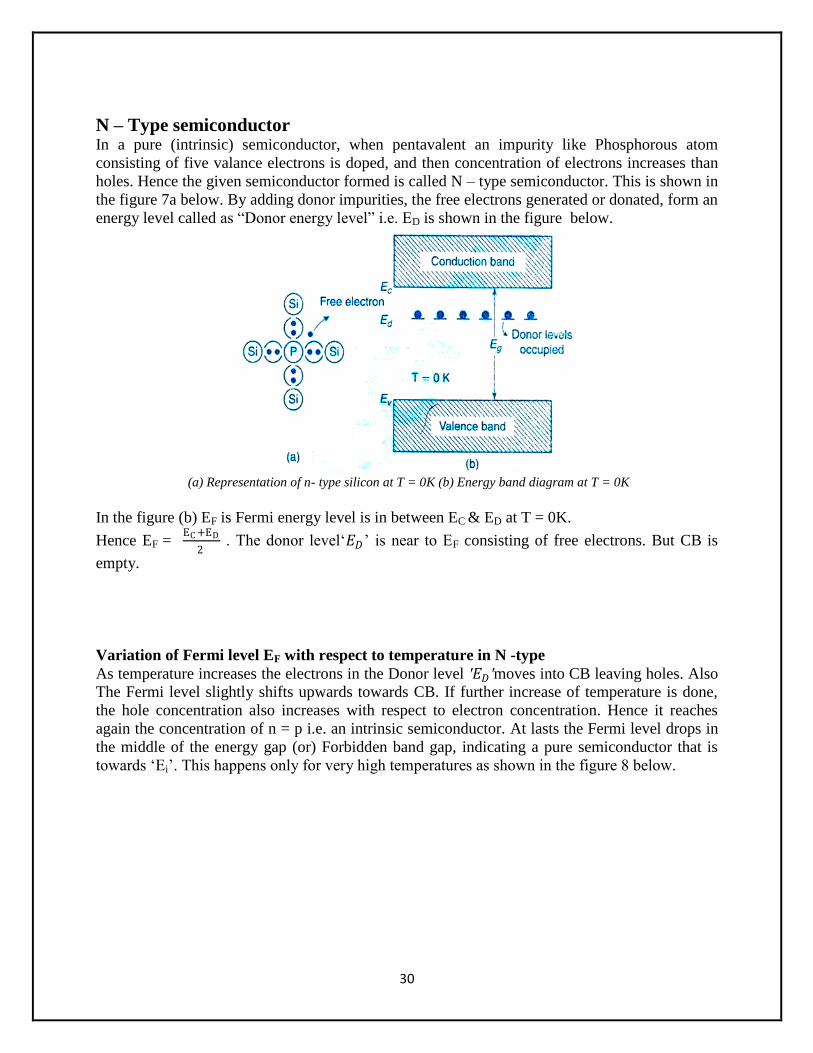
N – Type semiconductor In a pure (intrinsic) semiconductor, when pentavalent an impurity like Phosphorous atom
consisting of five valance electrons is doped, and then concentration of electrons increases than
holes. Hence the given semiconductor formed is called N – type semiconductor. This is shown in
the figure 7a below. By adding donor impurities, the free electrons generated or donated, form an
energy level called as “Donor energy level” i.e. ED is shown in the figure below.
(a) Representation of n- type silicon at T = 0K (b) Energy band diagram at T = 0K
In the figure (b) EF is Fermi energy level is in between EC & ED at T = 0K.
Hence EF = EC +ED
2 . The donor level„𝐸𝐷‟ is near to EF consisting of free electrons. But CB is
empty.
Variation of Fermi level EF with respect to temperature in N -type
As temperature increases the electrons in the Donor level ′𝐸𝐷 ′moves into CB leaving holes. Also
The Fermi level slightly shifts upwards towards CB. If further increase of temperature is done,
the hole concentration also increases with respect to electron concentration. Hence it reaches
again the concentration of n = p i.e. an intrinsic semiconductor. At lasts the Fermi level drops in
the middle of the energy gap (or) Forbidden band gap, indicating a pure semiconductor that is
towards „Ei‟. This happens only for very high temperatures as shown in the figure 8 below.

31
Fig.8 Variation of Fermi level wrt temperature in n- type semiconductor
Variation of EF with respect to donor concentration
As the donor concentration increases the Fermi level decreases (lowers) as in case of intrinsic
semiconductor „Ei. This is shown in the figure below
Variation of Fermi level with temperature for different donor concentrations in an n-type semiconductor
Carrier concentration in N – type semiconductor & Density of electrons in CB
Let ND is the donor concentration (no. of donor atoms per unit volume). Let it be written as
Or written as = 𝑁𝐷exp [− 𝐸𝐹−𝐸𝐷
𝐾𝐵𝑇]
= 𝑁𝐷𝑒−(𝐸𝐹−𝐸𝐷 )
𝐾𝐵𝑇 →(1)
The density of electrons in CB in pure semiconductor is given by
= 2[2𝜋𝑚 𝑒
∗𝐾𝐵𝑇
2 ]3
2 𝑒−(𝐸𝐶−𝐸𝐹)
𝐾𝐵𝑇 → (2)
At very low temperatures the no. of electrons in CB must be equal to the no. of donor atoms per
unit volume. Hence equating equations (1) & (2) we get

32
2[2𝜋𝑚 𝑒
∗𝐾𝐵𝑇
2 ]3
2 𝑒−(𝐸𝐶−𝐸𝐹 )
𝐾𝐵𝑇 = 𝑁𝐷𝑒−(𝐸𝐹−𝐸𝐷 )
𝐾𝐵𝑇
𝑒
−(𝐸𝐶+𝐸𝐹 )𝐾𝐵𝑇
𝑒
−(𝐸𝐹+𝐸𝐷 )𝐾𝐵𝑇
= 𝑁𝐷
2[2𝜋𝑚 𝑒
∗𝐾𝐵𝑇
2 ]32
𝑒−𝐸𝐶+𝐸𝐹+𝐸𝐹−𝐸𝐷
𝐾𝐵𝑇 = 𝑁𝐷
2[2𝜋𝑚 𝑒
∗𝐾𝐵𝑇
2 ]32
𝑒2𝐸𝐹−(𝐸𝐶+𝐸𝐷 )
𝐾𝐵𝑇 = 𝑁𝐷
2[2𝜋𝑚 𝑒
∗𝐾𝐵𝑇
2 ]32
Taking logarithms on both sides we get
2𝐸𝐹−(𝐸𝐶+𝐸𝐷 )
𝐾𝐵𝑇 = log[
𝑁𝐷
2[2𝜋𝑚 𝑒
∗𝐾𝐵𝑇
2 ]32
]
2𝐸𝐹−(𝐸𝐶 + 𝐸𝐷) = 𝐾𝐵𝑇log[𝑁𝐷
2[2𝜋𝑚 𝑒
∗𝐾𝐵𝑇
2 ]3
2
]
𝐸𝐹 =(𝐸𝐶+𝐸𝐷 )
2+
𝐾𝐵𝑇
2log[
𝑁𝐷
2[2𝜋𝑚 𝑒
∗𝐾𝐵𝑇
2 ]32
] At T>0K→(3)
Case I: At T= 0K
𝐸𝐹 =(𝐸𝐶+𝐸𝐷 )
2 . That is EF lies between𝐸𝐶&𝐸𝐷
Case II: At T>0K. As temperature increases the Fermi level slightly shifts upwards towards CB,
hence 𝐸𝐹 =(𝐸𝐶+𝐸𝐷 )
2+
𝐾𝐵𝑇
2log[
𝑁𝐷
2[2𝜋𝑚 𝑒
∗𝐾𝐵𝑇
2 ]32
]
Density of electrons in CB in extrinsic semiconductor:
Here consider equation (2). That is
= 2[2𝜋𝑚𝑒
∗𝐾𝐵𝑇
2]
3
2 𝑒−(𝐸𝐶−𝐸𝐹 )
𝐾𝐵𝑇
OR
= 2[2𝜋𝑚𝑒
∗𝐾𝐵𝑇
2]
3
2 𝑒(𝐸𝐹−𝐸𝐶)
𝐾𝐵𝑇
Substitute the value of EF from equation (3) in equation (2), it becomes 𝑛(𝐸𝑥𝑡𝑟𝑖𝑛𝑠𝑖𝑐𝑁 −𝑡𝑦𝑝𝑒 )
𝑛(𝐸𝑥𝑡𝑟𝑖𝑛𝑠𝑖𝑐𝑁 −𝑡𝑦𝑝𝑒 ) = 2[2𝜋𝑚 𝑒
∗𝐾𝐵𝑇
2 ]3
2 exp
(𝐸𝐶+𝐸𝐷 )
2+
𝐾𝐵𝑇
2log
𝑁𝐷
2[2𝜋𝑚 𝑒
∗𝐾𝐵𝑇
2 ]32
−𝐸𝐶
𝐾𝐵𝑇
On simplifying
We know that exp (a + b) = exp (a) × exp (b)
Also exp (log x) = x
= 2[2𝜋𝑚 𝑒
∗𝐾𝐵𝑇
2 ]3
2 exp (𝐸𝐷−𝐸𝐶)
2𝐾𝐵𝑇
(𝑁𝐷 )12
(2)12
[2𝜋𝑚 𝑒∗𝐾𝐵𝑇
2 ]34
𝑛(𝐸𝑥𝑡𝑟𝑖𝑛𝑠𝑖𝑐𝑁 −𝑡𝑦𝑝𝑒 ) = (2𝑁𝐷)1
2 [2𝜋𝑚𝑒
∗𝐾𝐵𝑇
2]
3
4 exp −(𝐸𝐶 − 𝐸𝐷)
2𝐾𝐵𝑇
OR

33
𝑛(𝐸𝑥𝑡𝑟𝑖𝑛𝑠𝑖𝑐𝑁 −𝑡𝑦𝑝𝑒 ) = (2𝑁𝐷)1
2 [2𝜋𝑚𝑒
∗𝐾𝐵𝑇
2]
3
4 𝑒 −(𝐸𝐶−𝐸𝐷 )
2𝐾𝐵𝑇
P- type semiconductor
P – Type semiconductor is formed by doping with trivalent impurity atoms (acceptor) like III
rd
group atoms i.e. Aluminum, Gallium, and Indium etc to a pure semiconductor like Ge or Si. As
the acceptor trivalent atoms has only three valance electrons & Germanium , Silicon has four
valence electrons; holes or vacancy is created for each acceptor dopant atom. Hence holes are
majority and electrons are minority. It is shown in the figure a below. Also an acceptor energy
level „EA‟ is formed near VB consisting of holes, as shown in the figure below.
(a) Representation of p- type silicon at T = 0K (b) Energy band diagram at T =0K
As temperature increases (T>0K) the electrons in VB which are in covalent bonds break the
bonds become free and move from VB to acceptor energy level E A.
Variation of Fermi level EF with respect to temperature in P- type semiconductor
As temperature increases the Fermi level EF slightly drops towards VB. For further increase of
high temperatures the electron concentration also increases with respect to hole concentration.
Hence a condition is reached such that „n = p‟ i.e. it becomes an intrinsic or pure semiconductor.
Hence the Fermi level increases and reaches to intrinsic level Ei as in case of pure
semiconductor. This is shown in the figure below

34
Variation of Fermi level wrt temperature in p- type
Variation of Fermi level with respect to acceptor concentration:
Also as the acceptor concentration increases we find that Fermi level EF reaches (increases)
towards intrinsic level Ei as in case of pure or intrinsic semiconductor. This is shown in the figure
below.
Variation of Fermi level with temperature for different acceptor concentrations in a p-type
Carrier concentration of P- type semiconductor & Density of holes in VB
Let N A is the acceptor concentration (no. of acceptor atoms per unit volume). Let it be written as
= 𝑁𝐴exp [− 𝐸𝐴−𝐸𝐹
𝐾𝐵𝑇]
Or written as
= 𝑁𝐴𝑒(𝐸𝐹−𝐸𝐴 )
𝐾𝐵𝑇 → (1)
The density of holes in VB in pure semiconductor is given by
= 2[2𝜋𝑚 𝑃
∗ 𝐾𝐵𝑇
2 ]3
2 𝑒−(𝐸𝐹−𝐸𝑉 )
𝐾𝐵𝑇 →(2)

35
At very low temperatures the no. of holes in VB must be equal to the no. of acceptor atoms per
unit volume. Hence equating equations (1) & (2) we get
2[2𝜋𝑚 𝑝
∗ 𝐾𝐵𝑇
2]
3
2 𝑒(−𝐸𝐹+𝐸𝑉 )
𝐾𝐵𝑇 = 𝑁𝐴𝑒(𝐸𝐹−𝐸𝐴 )
𝐾𝐵𝑇
𝑒
(−𝐸𝐹+𝐸𝑉 )𝐾𝐵𝑇
𝑒
(𝐸𝐹−𝐸𝐴 )𝐾𝐵𝑇
= 𝑁𝐴
2[2𝜋𝑚 𝑃
∗ 𝐾𝐵𝑇
2 ]32
𝑒−𝐸𝐹+𝐸𝑉−𝐸𝐹+𝐸𝐴
𝐾𝐵𝑇 = 𝑁𝐴
2[2𝜋𝑚 𝑃
∗ 𝐾𝐵𝑇
2 ]32
𝑒−2𝐸𝐹+(𝐸𝑉 +𝐸𝐴 )
𝐾𝐵𝑇 = 𝑁𝐴
2[2𝜋𝑚 𝑃
∗ 𝐾𝐵𝑇
2 ]32
Taking logarithms on both sides we get
−2𝐸𝐹+(𝐸𝑉 +𝐸𝐴 )
𝐾𝐵𝑇 = log[
𝑁𝐴
2[2𝜋𝑚 𝑃
∗ 𝐾𝐵𝑇
2 ]32
]
−2𝐸𝐹+(𝐸𝑉 + 𝐸𝐴) = 𝐾𝐵𝑇log[𝑁𝐴
2[2𝜋𝑚 𝑃
∗ 𝐾𝐵𝑇
2 ]3
2
]
𝐸𝐹 =(𝐸𝑉+𝐸𝐴 )
2−
𝐾𝐵𝑇
2log[
𝑁𝐴
2[2𝜋𝑚 𝑃
∗ 𝐾𝐵𝑇
2 ]32
] At T>0K → (3)
Case I: At T= 0K
𝐸𝐹 =(𝐸𝑉+𝐸𝐴 )
2 .That is EF lies between𝐸𝑉&𝐸𝐴
Case II: At T>0K. As temperature increases the Fermi level slightly drops towards VB, hence
𝐸𝐹 =(𝐸𝑉 + 𝐸𝐴)
2−
𝐾𝐵𝑇
2log[
𝑁𝐴
2[2𝜋𝑚 𝑝
∗ 𝐾𝐵𝑇
2 ]3
2
]
Density of electrons in CB in extrinsic semiconductor
Here consider equation (2). That is
= 2[2𝜋𝑚𝑝
∗𝐾𝐵𝑇
2]
3
2 𝑒−(𝐸𝐹−𝐸𝑉 )
𝐾𝐵𝑇
OR
= 2[2𝜋𝑚𝑝
∗𝐾𝐵𝑇
2]
3
2 𝑒(−𝐸𝐹+𝐸𝑉 )
𝐾𝐵𝑇
Substitute the value of EF from equation (3) in equation (2), it becomes 𝑛(𝐸𝑥𝑡𝑟𝑖𝑛𝑠𝑖𝑐𝑃 −𝑡𝑦𝑝𝑒 )
𝑛(𝐸𝑥𝑡𝑟𝑖𝑛𝑠𝑖𝑐𝑃 −𝑡𝑦𝑝𝑒 ) = 2[2𝜋𝑚 𝑝
∗ 𝐾𝐵𝑇
2 ]3
2 exp
[−(𝐸𝑉 +𝐸𝐴 )
2+
𝐾𝐵𝑇
2log [
𝑁𝐴
2[2𝜋𝑚 𝑝
∗ 𝐾𝐵𝑇
2 ]32
]+𝐸𝑉
𝐾𝐵𝑇
On simplifying
We know that exp (a + b) = exp (a) × exp (b)
Also exp (log x) = x
= 2[2𝜋𝑚 𝑝
∗ 𝐾𝐵𝑇
2 ]3
2 exp (𝐸𝑉−𝐸𝐴 )
2𝐾𝐵𝑇
(𝑁𝐴 )12
(2)12
[2𝜋𝑚 𝑝∗ 𝐾𝐵𝑇
2 ]34
36
𝑛(𝐸𝑥𝑡𝑟𝑖𝑛𝑠𝑖𝑐𝑃 −𝑡𝑦𝑝𝑒 ) = (2𝑁𝐴)1
2 [2𝜋𝑚𝑝
∗𝐾𝐵𝑇
2]
3
4 exp −(𝐸𝐴 − 𝐸𝑉)
2𝐾𝐵𝑇
OR
𝑛(𝐸𝑥𝑡𝑟𝑖𝑛𝑠𝑖𝑐𝑃 −𝑡𝑦𝑝𝑒 ) = (2𝑁𝐴)1
2 [2𝜋𝑚 𝑝
∗ 𝐾𝐵𝑇
2]
3
4 𝑒 −(𝐸𝐴−𝐸𝑉 )
2𝐾𝐵𝑇
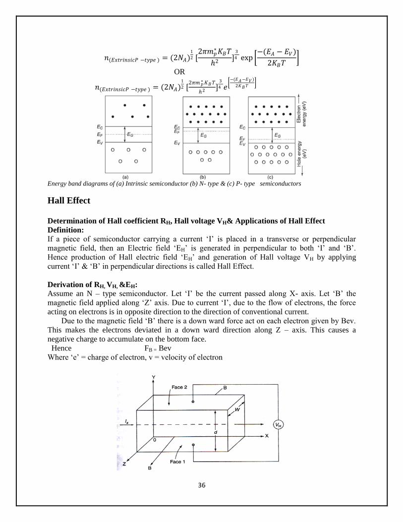
Energy band diagrams of (a) Intrinsic semiconductor (b) N- type & (c) P- type semiconductors
Hall Effect
Determination of Hall coefficient RH, Hall voltage VH& Applications of Hall Effect
Definition:
If a piece of semiconductor carrying a current „I‟ is placed in a transverse or perpendicular
magnetic field, then an Electric field „EH‟ is generated in perpendicular to both „I‟ and „B‟.
Hence production of Hall electric field „EH‟ and generation of Hall voltage VH by applying
current „I‟ & „B‟ in perpendicular directions is called Hall Effect.
Derivation of RH, VH, &EH:
Assume an N – type semiconductor. Let „I‟ be the current passed along X- axis. Let „B‟ the
magnetic field applied along „Z‟ axis. Due to current „I‟, due to the flow of electrons, the force
acting on electrons is in opposite direction to the direction of conventional current.
Due to the magnetic field „B‟ there is a down ward force act on each electron given by Bev.
This makes the electrons deviated in a down ward direction along Z – axis. This causes a
negative charge to accumulate on the bottom face.
Hence FB = Bev
Where „e‟ = charge of electron, v = velocity of electron

37
A semiconductor applied to current and magnetic field perpendicularly in Hall Effect
A potential difference is formed from top to bottom of the specimen. The potential difference
causes a field EH to flow along negative Y- axis. Due to EH along negative Y- direction a force of
eEH acts in upward direction along positive Y- axis.
Hence FE = e EH
Under equilibrium condition
Upward force due to EH = Downward force due to B.
FB = FE
e EH = Bev
v = 𝐸𝐻
𝐵 → (1)
If J is the current density then J = nev
v = 𝐽
𝑛𝑒 →(2)
Equating (1) & (2) we get 𝐸𝐻
𝐵 =
𝐽
𝑛𝑒
EH = 𝐽𝐵
𝑛𝑒
EH =[−1
𝑛𝑒] B J
Let Hall coefficient RH = −1
𝑛𝑒 for electrons
RH = −1
𝑝𝑒 for holes
Hence EH = RH B J → (4)
RH = 𝐸𝐻
B J →(5)
Where n= electron density, P = hole density, EH = Hall electric field, RH = Hall coefficient
B = magnetic field, J = current density
Experimental determination of RH
Consider equation (5)
RH = 𝐸𝐻
B J
Let VH is the Hall voltage across the sample of thickness„t‟
Generally V = Ed
In Hall effect VH = EH × t
EH = 𝑉𝐻
𝑡 →(6)
If „b‟ is the width of the sample semiconductor, Area „A‟, thickness„t‟
Area = breadth × thickness
A = b × t
We know that current density J = 𝐼
𝐴
J = 𝐼
𝑏𝑡 → (7)
Substituting equations (6) & (7) in (5) we get
RH = [𝑉𝐻𝑡
]
𝐵[𝐼
𝑏𝑡]
38
Hall coefficient RH = VH × b
𝐵×𝐼 → (8)
Where VH = Hall voltage, b = breadth of a semiconductor, B = magnetic field
I = current due to flow of electron
VH = 𝑅𝐻𝐵𝐼
𝑏 → (9)
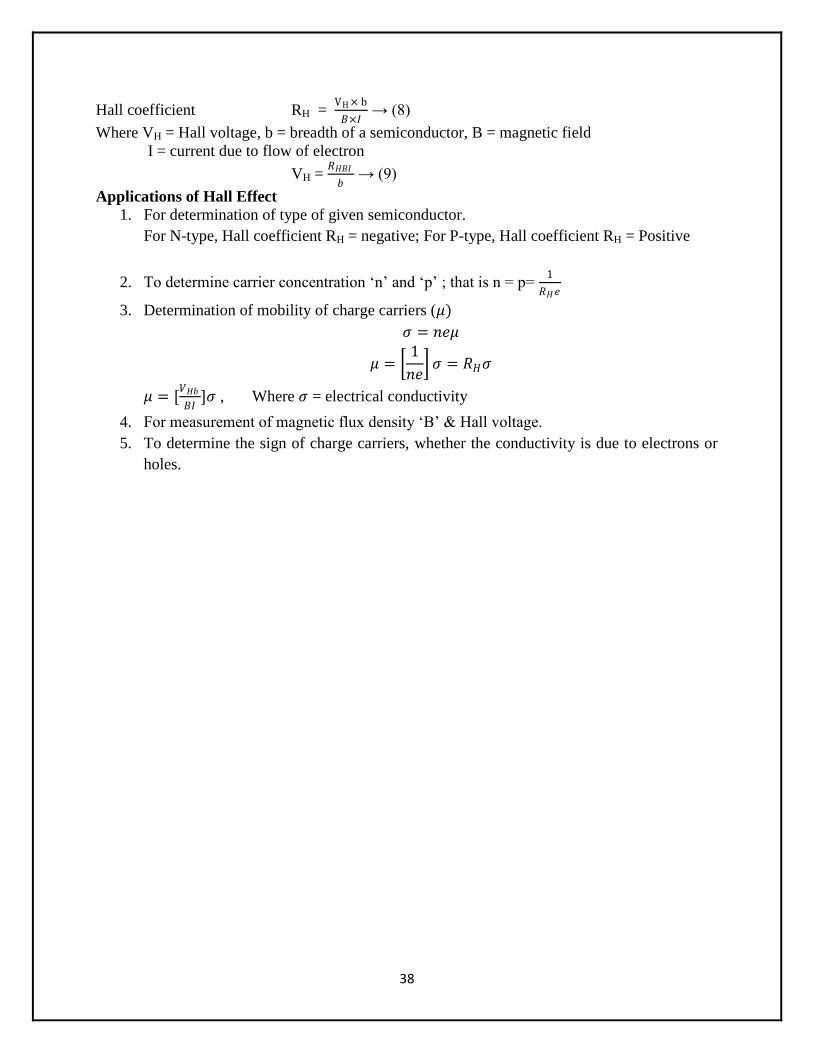
Applications of Hall Effect
1. For determination of type of given semiconductor.
For N-type, Hall coefficient RH = negative; For P-type, Hall coefficient RH = Positive
2. To determine carrier concentration „n‟ and „p‟ ; that is n = p= 1
𝑅𝐻𝑒
3. Determination of mobility of charge carriers (𝜇)
𝜎 = 𝑛𝑒𝜇
𝜇 = 1
𝑛𝑒 𝜎 = 𝑅𝐻𝜎
𝜇 = [𝑉𝐻𝑏
𝐵𝐼]𝜎 , Where 𝜎 = electrical conductivity
4. For measurement of magnetic flux density „B‟ & Hall voltage.
5. To determine the sign of charge carriers, whether the conductivity is due to electrons or
holes.

39
UNIT-III
LASERS AND FIBER OPTICS
Introduction LASER stands for light amplification by stimulated emission of radiation. It is different
from conventional light (such as tube light or electric bulb), there is no coordination among
different atoms emitting radiation. Laser is a device that emits light (electromagnetic radiation)
through a process is called stimulated emission.
Spontaneous and stimulated emission In lasers, the interaction between matter and light is of three different types. They are:
absorption, spontaneous emission and stimulates emission.Let E1 and E2 be ground and
excited states of an atom. The dot represents an atom. Transition between these states
involves absorption and emission of a photon of energy E2-E1=hν12. Where „h‟ is Planck‟s
constant.
(a) Absorption: As shown in fig8.1(a), if a photon of energy hν12(E2-E1) collides with an
atom present in the ground state of energy E1 then the atom completely absorbs the
incident photon and makes transition to excited state E2.
(b) Spontaneous emission:As shown in fig8. 1. (b), an atom initially present in the excited
state makes transition voluntarily on its own. Without any aid of external stimulus or an
agency to the ground. State and emits a photon of energy hν12(=E2-E1).this is called
spontaneous emission. These are incoherent.
(c) Stimulated emission:As shown in fig8.1.(c), a photon having energy hν12(E2-
E1)impinges on an atom present in the excited state and the atom is stimulated to make
transition to the ground state and gives off a photon of energy hν12. The emitted photon is
in phase with the incident photon. These are coherent. This type of emission is known as
stimulated emission.

40
Fig.2.1 (a) Absorption ;(b) Spontaneous emission;(c) Stimulated emission
Differences between Spontaneous emission and stimulated emission of
radiation
Spontaneous emission Stimulated emission
1. Polychromatic radiation
2. Less intensity
3. Less directionality, more angular
spread during propagation
4. Spatially and temporally in
coherent radiation
5. Spontaneous emission takes place
when excited atoms make a
transition to lower energy level
voluntarily without any external
stimulation.
1. Monochromatic radiation
2. High intensity
3. High directionality, so less angular
spread during propagation.
4. Specially and temporally coherent
radiation.
5. Stimulated emission takes place
when a photon of energy equal to
h ν12(=E2-E1)stimulates an excited
atom to make transition to lower
energy level.
Characteristics of Laser Light
(i).Coherence:Coherence is one of the unique properties of laser light. It arises from the
stimulated emission process. Since a common stimulus triggers the emission events which
provide the amplified light, the emitted photons are in step and have a definite phase relation to
each other. This coherence is described interms of temporal and spatial coherence.
(ii). Monochromaticity:A laser beam is more or less in single wave length. I.e. the line width of
laser beams is extremely narrow. The wavelengths spread of conventional light sources is usually
1 in 106, where as in case of laser light it will be 1 in 10
5.I.e. if the frequency of radiation is
1015
Hz., then the width of line will be 1 Hz. So, laser radiation is said to be highly
monochromatic. The degree of non-monochromaticity has been expressed as
ξ =(dλ/λ) =dν/ν, where dλ or dν is the variation in wavelength or variation in
frequency of radiation.
(iii) Directionality:Laser beam is highly directional because laser emits light only in one
direction. It can travel very long distances without divergence. The directionality of a laser beam
has been expressed interms of divergence. Suppose r1 and r2 are the radii of laser beam at
distances D1 and D2 from a laser, and then we have.
Then the divergence, ∆θ= (r1 - r2)/ D2-D1
The divergence for a laser beam is 0.01mille radian where as incase of search light it is 0.5
radian.
(iv)High intensity:In a laser beam lot of energy is concentrated in a small region. This
concentration of energy exists both spatially and spectrally, hence there is enormous intensity for
laser beam. The power range of laser is about 10-13
w for gas laser and is about 109 w for pulsed
solid state laser and the diameter of the laser beam is about 1 mm. then the number of photons
coming out from a laser per second per unit area is given by
Nl=P/ hνπr2≈1022to1034photons/m
-2-sec
By assuminghν=10-19
Joule,Power P=10-3
to109watt r=0.5×10
-3meter

41
Based on Planck‟s black body radiation, the number of photons emitted per second per unit area
by a body with temperature T is given by
Nth= (2hπC/ λ4)(1/e
(hν/kT
)-1) dλ≈10
16photons/m
2.sec
By assuming T=1000k, λ=6000A0
This comparison shows that laser is a highly intensive beam.
Population inversion
Usually in a system the number of atoms (N1) present in the ground state (E1) is larger than the
number of atoms(N2) present in the higher energy state. The process of making N2>N1 called
population inversion. Conditions for population inversion are:
a) The system should posses at least a pair of energy levels(E2>E1), separated by an energy
of equal to the energy of a photon (hν).
b) There should be a continuous supply of energy to the system such that the atoms must be
raised continuously to the excited state.
Population inversion can be achieved by a number of ways. Some of them are (i) optical
pumping (ii) electrical discharge (iii) inelastic collision of atoms (iv) chemical reaction and
(v) direct conversion
Helium-Neongas laser Helium-Neon gas laser is a continuous four level gas laser. It consists of a long, narrow
cylindrical tube made up of fused quartz. The diameter of the tube will vary from 2 to 8 mm and
length will vary from 10 to 100 cm. The tube is filled with helium and neon gases in the ratio of
10:1. The partial pressure of helium gas is 1mm of Hg and neon gas is 0.1mm of Hg so that the
pressure of the mixture of gases inside the tube is nearly 1 mm of Hg.
Laser action is due to the neon atoms.Helium is used for selective pumping of neon atoms
to upper energy levels. Two electrodes are fixed near the ends of the tube to pass electric
discharge through the gas. Two optically plane mirrors are fixed at the two ends of the tube at
Brewster angle normal to its axis. One of the mirrors is fully silvered so that nearly
100%reflection takes place and the other is partially silvered so that 1%of the light incident on it
will be transmitted. Optical resources column is formed between these mirrors.
. Fig.2.3 Helium-Neon gas laser
Working
When a discharge is passed through the gaseous mixture, electrons are accelerated down
the tube. These accelerated electrons collide with the helium atoms and excite them to higher
energy levels. The different energy levels of Helium atoms and Neon atoms is shown in
fig.2.3 the helium atoms are excited to the levels F2 and F3 these levels happen to be meta
stable energy states.

42
Energy levels and hence Helium atoms exited levels spend sufficiently large amount of
time before getting de excited. As shown in the fig 2.5(a), some of the excited states of neon
can correspond approximately to the same energy of excited levels F2 and F3. Thus, when
Helium atoms in level F2 and F3 collide with Neon atoms in the ground level E1, an energy
exchange takes place. This results in the excitation of Neon atoms to the levels E4 and E6and
de excitation of Helium atoms to the ground level (F1). Because of long life times of the
atoms in levels F2 and F3, this process of energy transfer has a high probability. Thus the
discharge through the gas mixture continuously populates the neon atoms in the excited
energy levels E4 and E6. This helps to create a state of population inversion between the
levels E4 (E6) to the lower energy level (E3 and E5). The various transitions E6→E5, E4→E3,
E6→E3 leads to the emission of wave lengths 3.39mm, 1.15 um and 6328 A0. Specific
frequency selection may be obtained by employing mirrors
The excited Neon atoms drop down from the level E3 to the E2 by spontaneously emitting
a photon around wavelength 6000A0. The pressures of the two gases in the mixture are so
chosen that there is an effective transfer of energy from the Helium to the Neon atoms. Since
the level E2 is a meta stable state, there is a finite probability of the excitation of Neon, atoms
from E2 to E3 leading to population inversion, when a narrow tube is used, the neon atoms in
the level E2 collide with the walls of the tube and get excited to the level E1. The transition
from E5 to E3 may be non radioactive. The typical power outputs of He-Ne laser lie between
1 and 50 mw of continuous wave for inputs of 5-10W.
Fig.2.4. Energy level diagram of He-Ne atoms.
Ruby Laser
Ruby Laser is a solid state pulsed, three level lasers. It consists of a cylindrical shaped
ruby crystal rod of length varying from 2 to 20cms and diameter varying 0.1 to 2cms. This end
faces of the rod are highly flat and parallel. One of the faces is highly silvered and the other face
is partially silvered so that it transmits 10 to 25% of incident light and reflects the rest so as to
make the rod-resonant cavity. Basically, ruby crystal is aluminum oxide [Al 2O3] doped with
0.05 to 0.5% of chromium atom. These chromium atoms serve as activators. Due to presence of
0.05% of chromium, the ruby crystal appears in pink color. The ruby crystal is placed along the
axis of a helical xenon or krypton flash lamp of high intensity.

43
Fig.2.5 Ruby laser
Fig.2.6 Energy level diagram of chromium ions in a ruby crystal
Construction: Ruby (Al2O3+Cr2O3) is a crystal of Aluminum oxide in which some of Al
+3 ions are
replaced by Cr +3
ions.When the doping concentration of Cr+3
is about 0.05%, the color of the
rod becomes pink. The active medium in ruby rod is Cr+3
ions. In ruby laser a rod of 4cm long
and 5mm diameter is used and the ends of the rod are highly polished. Both ends are silvered
such that one end is fully reflecting and the other end is partially reflecting.
The ruby rod is surrounded by helical xenon flash lamp tube which provides the optical
pumping to raise the Chromium ions to upper energy level (rather energy band). The xenon
flash lamp tube which emits intense pulses lasts only few milliseconds and the tube
consumes several thousands of joules of energy. Only a part of this energy is used in
pumping Chromium ions while the rest goes as heat to the apparatus which should be cooled
with cooling arrangements as shown in fig.2.5. The energy level diagram of ruby laser is
shown in fig.2.6
Working:

44
Ruby crystal is made up of aluminum oxide as host lattice with small percentage of
Chromium ions replacing aluminum ions in the crystal chromium acts as do pant. A do pant
actually produces lasing action while the host material sustains this action. The pumping
source for ruby material is xenon flash lamp which will be operated by some external power
supply. Chromium ions will respond to this flash light having wavelength of 5600A0. When
the Cr +3
ions are excited to energy level E3 from E1 the population in E3 increases. Chromium
ions stay here for a very short time of the order of 10-8 seconds then they drop to the level E2
which is mat stable state of life time 10-3
s. Here the level E3is rather a band, which helps the
pumping to be more effective. The transitions from E3toE2 are non-radioactive in nature.
During this process heat is given to crystal lattice. Hence cooling the rod is an essential
feature in this method. The life time in mete stable state is 10 5times greater than the lifetime
in E3. As the life of the state E2 is much longer, the number of ions in this state goes on
increasing while ions. In this state goes on increasing while in the ground state (E1)goes on
decreasing. By this process population inversion is achieved between the exited Meta stable
state E2 and the ground state E1. When an excited ion passes spontaneously from the
metastable state E2 to the ground state E1, it emits a photon of wave length 6943A0. This
photon travels through the rod and if it is moving parallel to the axis of the crystal, is
reflected back and forth by the silvered ends until it stimulates an excited ion in E2 and
causes it to emit fresh photon in phase with the earlier photon. This stimulated transition
triggers the laser transition. This process is repeated again and again because the photons
repeatedly move along the crystal being reflected from its ends. The photons thus get
multiplied. When thephoton beam becomes sufficiently intense, such that part of it emerges
through the partially silvered end of the crystal.
Drawbacks of ruby laser:
1. The laser requires high pumping power to achieve population inversion.
2. It is a pulsed laser.
. Fig.2.7 the output pulses with time.
Applications of Lasers Lasers find applications in various fields. They are described below.
a) In Communications :
Lasers are used in optical fiber communications. In optical fiber communications, lasers are used as
light source to transmit audio, video signals and data to long distances without attention and
distortion.

45
b) The narrow angular spread of laser beam can be used for communication between earth and
moon or to satellites.
c) As laser radiation is not absorbed by water, so laser beam can be used in under water (inside
sea) communication networks.
2.Industrial Applications
a) Lasers are used in metal cutting, welding, surface treatment and hole drilling. Using lasers
cutting can be obtained to any desired shape and the curved surface is very smooth.
b) Welding has been carried by using laser beam.
c) Dissimilar metals can be welded and micro welding is done with great case.
d) Lasers beam is used in selective heat treatment for tempering the desired parts in
automobile industry
e) Lasers are widely used in electronic industry in trimming the components of ICs
3. Medical Applications 1. Lasers are used in medicine to improve precision work like surgery. Brain surgery is an
example of precision surgery Birthmarks, warts and discoloring of the skin can easily be
removed with an unfocussed laser. The operations are quick and heal quickly and, best of all,
they are less painful than ordinary surgery performed with a scalpel.
2. Cosmetic surgery (removing tattoos, scars, stretch marks, sunspots,wrinkles,birthmarks and
hairs) see lasers hair removal.
3.Laser types used in dermatology include ruby(694nm),alexandrite(755nm),pulsed diode
array(810nm), Nd:YAG(1064nm), HO:YAG(2090nm), and Er:YAG(2940nm)
4. Eye surgery and refracting surgery.
5. Soft tissue surgery: Co2 Er:YAGlaser.
6. Laser scalpel (general surgery, gynecological, urology, laparoscopic).
7. Dental procedures.
8. Photo bio modulation (i.e. laser therapy)
9. “No-touch” removal of tumors, especially of the brain and spinal cord.
10. In dentistry for caries removal, endodontic/periodontic, procedures, tooth whitening, and
oral surgery.
4. Military Applications
The various military applications are:
a) Death rays:By focusing high energetic laser beam for few seconds to aircraft, missile, etc
can be destroyed. So, these rays are called death rays or war weapons.
b) Laser gun:The vital part of energy body can be evaporated at short range by focusing
highly convergent beam from a laser gun.
c) LIDAR (Light detecting and ranging):In place of RADAR, we can use LIDAR to
estimate the size and shape of distant objects or war weapons. The differences between
RADAR and LIDAR are that, in case of RADAR, Radio waves are used where as incase of
LIDAR light is used.
5.In Computers:By using lasers a large amount of information or data can be stored in CD-
ROM or their storage capacity can be increased. Lasers are also used in computer printers.

46
6.In Thermonuclear fusion:Toinitiate nuclear fusion reaction, very high temperature and
pressure is required. This can be created by concentrating large amount of laser energy in a small
volume. In the fusion of deuterium and tritium, irradiation with a high energy laser beam pulse
of 1 nano second duration develops a temperature of 10170
c, this temperature is sufficient to
initiate nuclear fusion reaction.
7.In Scientific Research:In scientific, lasers are used in many ways including
a) A wide variety of interferometrie techniques.
b) Raman spectroscopy.
c) Laser induced breakdown spectroscopy.
d) Atmospheric remote sensing.
e) Investigating non linear optics phenomena
f) Holographic techniques employing lasers also contribute to a number of measurement
techniques.
g) Laser (LADAR) technology has application in geology, seismology, remote sensing and
atmospheric physics.
h) Lasers have been used abroad spacecraft such as in the cassini-huygens mission.
i) In astronomy lasers have been used to create artificial laser guide stars, used as reference
objects for adaptive optics telescope.
FIBER OPTICS
Introduction 1. An optical fiber (or fiber) is a glass or plastic fiber that carries light along its length.
2. Fiber optics is the overlap of applied science and engineering concerned with the design and
application of optical fibers.
3. Optical fibers are widely used in fiber-optic communications, which permits transmission over
long distances and at higher band widths (data rates) than other forms of communications.
4. Specially designed fibers are used for a variety of other applications, including sensors and
fiber lasers. Fiber optics, though used extensively in the modern world, is a fairly simple and old
technology.
Principle of Optical Fiber Optical fiber is a cylinder of transparent dielectric medium and designed to guide visible
and infrared light over long distances. Optical fibers work on the principle of total
internalreflection.
Optical fiber is very thin and flexible medium having a cylindrical shape consisting of three
sections
1) The core material
2) The cladding material
3) The outer jacket
The structure of an optical is shown in figure. The fiber has a core surrounded by a cladding
material whose reflective index is slightly less than that of the core material to satisfy the
condition for total internal reflection. To protect the fiber material and also to give mechanical
support there is a protective cover called outer jacket. In order to avoid damages there will be
some cushion between cladding protective cover.

47
Fig..Structure of an optical fiber
When a ray of light passes from an optically denser medium into an optically rarer
medium the refracted ray bends away from the normal. When the angle of incidence is increased
angle of refraction also increases and a stage is reached when the refracted ray just grazes the
surface of separation of core and cladding. At this position the angle of refraction is 90 degrees.
This angle of incidence in the denser medium is called the critical angle (θc) of the denser
medium with respect to the rarer medium and is shown in the fig. If the angle of incidence is
further increased then the totally reflected. This is called total internal reflection. Let the
reflective indices of core and cladding materials be n1 and n2 respectively.
Fig. Total internal reflection.
When a light ray, travelling from an optically denser medium into an optically rarer
medium is incident at angle greater than the critical angle for the two media. The ray is totally
reflected back into the medium by obeying the loss of reflection. This phenomenon is known as
totally internal reflection.
According to law of refraction,
n1 sinθ1= n 2 sinθ2
Here θ1=θc, θ2=90
n 1 sinθc=n2 sin 90

48
Sinθc = 𝑛2
𝑛1
θc = sinˉ¹(𝑛2
𝑛1) →(1)
Equation (1) is the expression for condition for total internal reflection. In case of total
internal reflection, there is absolutely no absorption of light energy at the reflecting surface.
Since the entire incident light energy is returned along the reflected light it is called total internal
reflection. As there is no loss of light energy during reflection, hence optical fibers are designed
to guide light wave over very long distances.
Acceptance Angle and Acceptance Cone Acceptance angle:Itis the angle at which we have to launch the beam at its end to enable the
entire light to propagate through the core. Fig.8.12 shows longitudinal cross section of the launch
of a fiber with a ray entering it. The light is entered from a medium of refractive index n0 (for air
n0=1) into the core of refractive index n1. The ray (OA) enters with an angle of incidence to the
fiber end face i.e. the incident ray makes angle with the fiber axis which is nothing but the
normal to the end face of the core. Let a right ray OA enters the fiber at an angle to the axis of
the fiber. The end at which light enter the fiber is called the launching pad.
Fig. Path of atypical light ray launched into fiber.
Let the refractive index of the core be n1 and the refractive index of cladding be n2. Here n1>n2.
The light ray reflects at an angle and strikes the core cladding interface at angle θ. If the angleθ
is greater than its critical angle θc, the light ray undergoes total internal reflection at the
interface.
According to Snell‟s law
n0sinαi=n1sinαr→ (2)
From the right angled triangle ABC
αr+θ=900
αr=900 –θ → (3)
Substituting (3) in (2), we get
n0sinαi =n1sin (900 –θ) = n1cos θ

49
sinαi=(𝑛1
𝑛0) cos θ →(4)
When θ= θc, αi= αm=maximum α value
sinαm=(𝑛1
𝑛0) cos θc→(5)
From equation (1) Sinθc = 𝑛2
𝑛1
cos θc= 1 − 𝑠𝑖𝑛2θc = 1 − (𝑛2
𝑛1)2 =
𝑛12−𝑛2
2
𝑛1 →(6)
Substitute equation (6) in equation (5)
sinαm=(𝑛1
𝑛0) 𝑛1
2−𝑛22
𝑛1 =
𝑛12−𝑛2
2
𝑛0 →(7)
If the medium surrounding fiber is air, then n0=1
sinαm= 𝑛12 − 𝑛2
2 →(8)
This maximum angle is called the acceptance angle or the acceptance cone half angle of the
fiber.
The acceptance angle may be defined as the maximum angle that a light ray can have with the
axis of the fiber and propagate through the fiber. Rotating the acceptance angle about the fiber
axis (fig.) describes the acceptance cone of the fiber. Light launched at the fiber end within this
acceptance cone alone will be accepted and propagated to the other end of the fiber by total
internal reflection. Larger acceptance angles make launching easier. Light gathering capacity of
the fiber is expressed in terms of maximum acceptance angle and is termed as “Numerical
Aperture”.
Fig. Acceptance cone
Numerical Aperture Numerical Aperture of a fiber is measure of its light gathering power. The numerical
aperture (NA) is defined as the sign of the maximum acceptance angle.
Numerical aperture (NA)= sinαm= 𝑛12 − 𝑛2
2 →(9)
= (𝑛1 − 𝑛2) (𝑛1 + 𝑛2)
= ((𝑛1 + 𝑛2) 𝑛1∆) → (10)

50
Where ∆= (𝑛1−𝑛2)
𝑛1called as fractional differences in refractive indices 𝑛 and 𝑛2are the
refractive indices of core and cladding material respectively.
As n1≈ n2, we can take n1+ n2= 2n1
Then numerical aperture= (2n12∆)
1/2= n1 (2∆)
1/2→ (11)
Numerical aperture is a measure of amount of light that can be accepted by a fiber. From
equation (9) it is seen that numerical aperture depends only on the refractive indices of core and
cladding materials and it is independent on the fiber dimensions. Its value ranges from 0.1 to 0.5.
A large NA means that the fiber will accept large amount of light from the source.
Proof: We shall show that the light emitted by a small defuse source situated on the fiber axis near to
one end face, only a fractionNA2 can be collected by the fiber and propagated along the fiber.
Consider a small defuse light source such as the isotropic radiator in which the power radiated
per unit solid angle in a direction θ to the normal to the surface
is given by
Fig. Diffuse light source
I(θ) =I0Cos θ→ (12)
The total power φ0 emitted such source is obtained by integrating I (θ) over all forward directions
φ0 = 𝐼0П/2
0 Cosθd θ → (13)
Where dΩ=small element of solid angle=2πSinθ dθ → (14)
φ0 = 𝐼0П/2
0 Cosθ2πSinθ d θ
= 𝜋𝐼0𝑆𝑖𝑛2θdθП/2
0=πI0→ (15)
But the power from such source that can be collected by an adjacent fiber whose core diameter
is greater than the diameter of the source is given by φ, where
Φ= 𝐼0𝛼𝑚
0 Cosθ2ПSinθ dθ
=П𝐼0sin2αm
(Φ /φ0)= (sinαm) 2
= (NA) 2
=2n12∆ → (16)
Where ∆= (𝑛1−𝑛2)
𝑛1
Equation (16) represents the light gathering power of the fiber. In order to collect as much light
as possible it is necessary to make n1 and ∆ large.
In some cases it is customary to use ∆n which can be defined as ∆n = n1- n2
But ∆= (𝑛1−𝑛2)
𝑛1=
∆n
𝑛1
(Φ /φ0)= (sinαm)2=(NA)
2=2n1∆n→(17)
NA= (2n1∆n) → (18)
Step index fibers and graded index fiber -transmission of signals in them:

51
Based on the variation of refractive index of core, optical fibers are divided into: (1) step index
and (2) graded index fibers. Again based on the mode of propagation, all these fibers are divided
into: (1) single mode and (2) multimode fibers. In all optical fibers, the refractive index of
cladding material is uniform. Now, we will see the construction, refractive index of core and
cladding with radial distance of fiber, ray propagation and applications of above optical fibers.
i. Step index fiber: The refractive index is uniform throughout the core of this fiber. As
we go radially in this fiber, the refractive index undergoes a step change at the core-
cladding interface. Based on the mode of propagation of light rays, step index fibers are
of 2 types: a) single mode step index fiber & b) multimode step index fibers. Mode
means, the number of paths available for light propagation of fiber. We describes the
different types of fiber below
a) Single mode step index fiber: The core diameter of this fiber is about 8 to
10µm and outer diameter of cladding is 60 to 70 µm. There is only one path for ray
propagation. So, it is called single mode fiber. The cross sectional view, refractive
index profile and ray propagation are shown in fig. (i). In this fiber, the
transmission of light is by successive total internal reflections i.e. it is a reflective
type fiber. Nearly 80% of the fibers manufactured today in the world are single
mode fibers. So, they are extensively used.
Fig (i).Single mode step index fiber ;( a) Cross sectional view and refractive index
profile ;( b) Ray propagation
Multimode step index fiber: The construction of multimode step index fiber is
similar to single mode step index fiber except that its core and cladding diameters are
much larger to have many paths for light propagation. The core diameter of this fiber
varies from 50 to 200 µm and the outer diameter of cladding varies from 100 to 250
µm. The cross-sectional view, refractive index profile and ray propagations are

52
shown in fig 2. Light propagation in this fiber is by multiple total internal reflections
i.e it is a reflective type fiber.
b) Transmission of signal in step index fiber: Generally the signal is
transmitted through the fiber in digital form i.e. in the form of 1‟s and 0‟s. The
propagation of pulses through the multimode fiber is shown in fig (i)(b). The pulse
which travels along path 1(straight) will reach first at the other end of fiber. Next
the pulse that travels along with path 2(zig-zag) reaches the other end. Hence, the
pulsed signal received at the other end is broadened. This is known as intermodal
dispersion. This imposes limitation on the separation between pulses and reduces
the transmission rate and capacity. To overcome this problem, graded index fibers
are used.
2) Graded index fiber: In this fiber, the refractive index decreases continuously from center
radially to the surface of the core. The refractive index is maximum at the center and minimum at
the surface of core. This fiber can be single mode or multimode fiber. The cross sectional view,
refractive index profile and ray propagation of multimode graded index fiber are shown in fig
.(ii)(a). The diameter of core varies from 50 to 200µm and outer diameter of cladding varies
from 100 to 250 µm.
The refractive index profile is circularly symmetric. As refractive index changes continuously
radially in core, light rays suffer continuous refraction in core. The propagation of light ray is not
due to total internal reflection but by refraction as shown in fig. (ii)(b). in graded index fiber,
light rays travel at different speed in different paths of the fiber. Near the surface of the core, the
refractive index is lower, so rays near the outer surface travel faster than the rays travel at the
center. Because of this, all the rays arrive at the receiving end of the fiber approximately at the
same time. This fiber is costly. .
Transmission of signal graded index fiber: In multimode graded index fiber, large
number of paths is available for light ray propagation. To discuss about inter modal dispersion,
we consider ray path 1 along the axis of fiber.

53
Fig. (ii).Multimode step index fibre(a)Cross sectional view and refractive index profle(b)Ray
propagation
As shown in fig. (ii)(b) and another ray path 2. Along with the axis of fiber, the refractive index
of core is maximum, so the speed of ray along path 1 is less. Path 2 is sinusoidal and it is longer,
along this path refractive index varies. The ray mostly travels in low refractive region, so the ray
2 moves slightly faster. Hence, the pulses of signals that travel along path 1 and path 2 reach
other end of fiber simultaneously. Thus, the problem of intermodal dispersion can be reduced to
a large extent using graded index fibers.
Differences between step index fiber and graded index fibers:
Step index fiber Graded index fiber
1.The refractive index of core
Is uniform and step or abrupt
Change in refractive index
Takes place at the interface of core
and cladding in step index fibers
1.The refractive index of core is non uniform, the
refractive index of core decreases Para-
Felicity from the axis of the fiber to its surface.
2. The light rays propagate in zigzag manner inside
the core. The rays travel in the fiber as meridional
rays they cross the fiber axis for every reflection.
2. Light rays propagate in the form of skew rays or
helical rays. They will not cross the fiber axis
Difference between single mode fibers and multi mode fibers:
Single mode fiber Multimode fiber 1. In single mode fiber there is only one
path for ray propagation
1. In multimode fiber, large number of
paths is available for light ray
propagation.
2. A single mode step index fiber has less
core diameter (< 10 µm) and the
difference between the reflective
indices of core and cladding is very
small.
2. Multi mode fibers, large number of
paths are available for light ray
propagation.
3. In single mode fibers, there is no
dispersion.
3. There is signal distortion and dispersion
takes place in multimode fibers.
4. The band width is about 50 MHz for
multimode step index fiber where as it
is more than 1000 MHz km in case of
single mode step index fiber.
4. The band width of the fiber lies in
between 200 MHz km to 600 MHz km
even though theoretically it has an
infinite bandwidth.
5. NA of multimode step index fiber is
more where as in single mode step
index fibers, it is very less.
5. NA of graded index fibers is less.
6. Launching of light into single mode 6. Launching of light into multimode

54
fibers is difficult. fibers is easy.
7. Fabrication cost is very high. 7. Fabrication cost is less
Fiber optic communication system : Fiber oppticsessentially deals of with the communication(including voice signals,video signals
or digital data) by transmission of light through optical fibers. Optical fiber communication
system essentially consists of three parts:(a)transmitter (b) optical fiber and (c) receiver.The
transmitter includes modulator, encoder, light source, drive circuits and couplers. The receiver
includes amplifier and decoder,binary electrical signal and light decoder.
Fig. Block diagram represents optical fibre communication system
55
UNIT-IV
LIGHT AND OPTICS
INTERFERENCE AND DIFFRACTION
Interference-Introduction
Wave Theory of light attempts to understand the various optical phenomena exhibited by
light waves. Interference constituted the first proof of the wave nature of light. Thomas Young
first experimentally demonstrated interference in light waves. The superposition principle forms
the conceptual basis for the explanation of interference. To produce interference, the light waves
should be coherent, i.e., the light waves should have constant phase difference and same
frequencies.
Interference
When two or more light waves superimpose in the medium then according to
superposition principle, the resultant displacement at any point is equal to the algebraic sum of
the displacements due to individual waves. The variation of resultant displacement influences
amplitude variation, which causes intensity variations. This modification in the distribution of
intensity in the region of superposition is known as interference. When the resultant amplitude is
the sum of the amplitudes due to two light waves, the interference is constructive interference. If
the resultant amplitude is equal to the difference of two amplitudes, the interference becomes
destructive interference. The intensity variations are studied as interference fringes or patterns.
Conditions for Interference
1. The two light sources emitting light waves should be coherent.
2. The two sources must emit continuous light waves of same wavelengths and frequency.
3. The separation between the two sources should be small.
4. The distance between the two sources and the screen should be large.
5. To view interference fringes, the background should be dark.
6. The amplitudes of the light waves should be equal or nearly equal.
7. The sources should be narrow, i.e., they must be small.
8. The sources should be monochromatic.
Young's Double Slit Experiment
This is a classic example of interference effects in light waves. Two light rays pass through two
slits, separated by a distance d and strike a screen a distance, L , from the slits, as in Fig. 22.10.

56
Figure 22.10: Double slit diffraction
If d<<L then the difference in path length r1 - r2 travelled by the two rays is approximately:
r1 - r2 dsin
where θis approximately equal to the angle that the rays make relative to a perpendicular line
joining the slits to the screen.
If the rays were in phase when they passed through the slits, then the condition for constructive
interference at the screen is:
dsinθ= m ,m = 1, 2,...
whereas the condition for destructive interference at the screen is:
dsinθ= (m + ) ,m = 1, 2,...
The points of constructive interference will appear as bright bands on the screen and the points of
destructive interference will appear as dark bands. These dark and bright spots are called
interference fringes. Note:
In the case that y , the distance from the interference fringe to the point of the screen
opposite the center of the slits (see Fig.22.10) is much less than L ( y<<L ), one can use
the approximate formula:
sin y/L

57
so that the formulas specifying the y - coordinates of the bright and dark spots,
respectively are:
y B
m = bright spots
y D
m = dark spots
The spacing between the dark spots is
y=
If d<<L then the spacing between the interference can be large even when the wavelength
of the light is very small (as in the case of visible light). This give a method for
(indirectly) measuring the wavelength of light. (See Ex.6 at the end of this Chapter.)
The above formulas assume that the slit width is very small compared to the wavelength
of light, so that the slits behave essentially like point sources of light.
Conditions for Interference
Observable interference can take place if the following conditions are fulfilled:
(a) The two sources should emit, continuously, waves of some wave-length or frequency. While
driving conditions for maxima and minima, we have taken „I‟ for both the waves to be same.
(b) The amplitudes of the two waves should be either or nearly equal. A good contrast between a
maxima and minima can only be obtained if the amplitudes of two waves are equal or nearly
equal.

58
(c) The two sources should be narrow. A broader source can be supposed to be a combination of
a number of narrow sources assembled side-by-side. Interference patterns due to these narrow
sources may overlap each other.
(d) The sources should be close to each other. The fringe width varies inversely as distance „d‟
between the two sources. So, interference pattern will be more clear and distant if „d‟ is small.
(e) The two sources should be coherent one.
Young’s Double Slit Experiment
The phenomenon of interference was first observed and demonstrated by Thomas Young in
1801. The experimental set up is shown in figure.
Light from a narrow slit S, illuminated by a monochromatic source, is allowed to fall on two
narrow slits A and B placed very close to each other. The width of each slit isabout 0.03 mm and
they are about 0.3 mm apart. Since A and B are equidistant from S, light waves from S reach A
and B in phase. So A and Bacts as coherent sources.
Accordingto Huygen‟s principle, wavelets from A and B spread out and overlappingtakes place
to the right side of AB. When a screen XY is placed at a distance of about 1 meter from the slits,
equally spaced alternate bright and dark fringes appear on the screen. These are called
interference fringes or bands. Using an eyepiece, the fringes can be seendirectly. At P on the
screen, waves from A and B travel equal distancesand arrive in phase. These two waves
constructively interfere and bright fringe is observed at P. This is called central bright fringe.
When one of the slits is covered, the fringes disappear and there is uniform illumination on the
screen. This shows clearly that the bands are due to interference.
Let d be the distance between two coherent sources A and B of wavelength λ. A screen XY is
placed parallelto AB at a distance D from the coherent sources. C is the midpoint of AB. O is a
point on the screen equidistant from A and B. P is a point at a distance x from O, as shown in Fig

59
5.17. Waves from A and B meet at P in phase or out of phase depending upon the path difference
between two waves draw AM perpendicular to BP.
The path difference δ = BP – AP
AP = MP
δ = BP – AP = BP – MP = BM
In right angled? ABM, BM = d sin θ If θ is small,
sin θ = θ
The path difference δ = θ.d
In right angled triangle COP, tan θ = OP/CO = x/D
For small values of θ, tan θ = θ
Thus, the path difference δ = xd/D
Bright Fringes
By the principle of interference, condition for constructive interference is the path difference =
nλ
xd/D = nλ
Here, n = 0,1,2.....indicate the order of bright fringes
So, x = (D/d) nλ
This equation gives the distance of the nth
bright fringe from the point O.

60
Dark Fringes
By the principle of interference, condition for destructive interference is the
path difference = (2n-1)λ/2
Here, n = 1,2,3 … indicate the order of the dark fringes.
So, x = (D/d) [(2n – 1) λ/2]
This equation gives the distance of the nth
dark fringe from the point O. Thus, on the screen
alternate dark and bright bands are seen on either side of the central bright band.
Band Width (β)
The distance between any two consecutive bright or dark bands is called bandwidth.
The distance between (n+1)th
and nth
order consecutive bright fringes from O is given by,
xn+1 – xn = [(D/d) [(n+1) λ] – (D/d) [(n)λ]] = (D/d) λ
Bandwidth, β = (D/d) λ
Similarly, it can be proved that the distance between two consecutive dark bands are also equal
to (D/d) λ. Since bright and dark fringes are of same width, they are equispaced on either side of
central maximum.
Condition for Obtaining Clear and Broad Interference Bands

61
The screen should be as far away from the source as possible.
The wavelength of light used must be larger.
The two coherent sources must be as close as possible.
Interference in Thin Film by Reflection
When light is incident on a plane parallel thin film, some portion gets reflected from the
upper surface and the remaining portion is transmitted into the film. Again, some portion of the
transmitted light is reflected back into the film by the lower surface and emerges through the
upper surface. These reflected light beams superimpose with each other, producing interference
and forming interference patterns.
Fig Interference in thin film
Consider a transparent plane parallel thin film of thickness „t „ with refractive index 𝜇.
Let a monochromatic light ray AB be incident at an angle of incidence of „i‟ on the upper surface
of the film. BE and BC are the reflected and transmitted light rays. Let the angle of refraction is
„r‟. The ray BC will be reflected into the film and emerge through the film in the form of light
ray DF. These two light rays superimpose and depending upon the path difference between them,
they produce interference patterns.
To know the path difference, draw the normal DG to BE. From the points D and G onwards, the
light rays travel equal distances. By the time the light ray travels from B to G, the transmitted
light ray has to travel from B to C and C to D.
The path difference between light rays (1) and (2) is,
Path difference= 𝜇(BC+CD) in film – BG in air →(1)
Consider the ∆BCH, cos r = 𝐻𝐶
𝐵𝐶
BC = 𝐻𝐶
cos 𝑟 =
𝑡
cos 𝑟
Similarly, from ∆DCH, CD= 𝑡
cos 𝑟
BC = CD = 𝑡
cos 𝑟 →(2)

62
To calculate BG, first BD which is equal to (BH+HD) has to be obtained.
From ∆BHC tan r = 𝐵𝐻
𝐶𝐻 =
𝐵𝐻
𝑡
BH = t tan r
Similarly, HD = t tan r
BD = BH+ HD = 2t tan r (∵BH = HD) →(3)
From ∆ BGD, sin i = 𝐵𝐺
𝐵𝐷
BG=BD sin i = 2t tan r sini
From Snell‟s law, sin i = 𝜇 sin r
BG= 2 𝜇t tan r sin r →(4)
Substituting the above values in Eq. (1)
Path difference= 2𝜇𝑡
cos 𝑟 - 2 𝜇t tanr sinr
= 2𝜇𝑡
cos 𝑟 -
2𝜇𝑡 𝑠𝑖𝑛2 𝑟
cos 𝑟
= 2𝜇𝑡
cos 𝑟(1-𝑠𝑖𝑛2 𝑟)=
2𝜇𝑡
cos 𝑟𝑐𝑜𝑠2r
= 2𝜇t cos r →(5)
At the point B, reflection occurs from the upper surface of the thin film (denser medium). Light
ray (1) undergoes an additional phase change of 𝜋 or an additional path difference of𝜆
2
Total path difference = 2𝜇t cos r + 𝜆
2
When the path difference is equal to integral multiple of 𝜆 then the rays (1) and (2) meet in phase
and undergo constructive interference.
The condition for bright fringe is
2𝜇t cos r + 𝜆
2 = n 𝜆
2𝜇t cos r = (2n-1) 𝜆
2 where n= 0,1,2,3… →(6)
When the path difference is equal to half integral multiple of 𝜆 then the rays (1) and (2) meet in
out of phase and undergo destructive interference.
The condition for dark fringe is
2𝜇t cos r + 𝜆
2= (2n-1)
𝜆
2
2𝜇t cos r =n 𝜆 where n=0, 1, 2, 3… →(7)
Depending on the above conditions, the interference pattern consists of bright and dark fringes.
Newton’s Rings
Newton‟s rings are one of the best examples for the interference in a nonuniform thin
film. When a Plano-convex lens with its convex surface is placed on a plane glass plate, an air
film of increasing thickness is formed between the two. The thickness of the film at the point of
contact is zero. If monochromatic light is allowed to fall normally and the film is viewed in the
reflected light, alternate dark and bright rings concentric around the point of contact between the
lens and glass plate are seen. These circular rings were discovered by Newton and are called
Newton‟s rings.

63
Experimental Arrangement
Fig Newton’s rings (Experimental set up)
The experimental arrangement is as shown in fig. The Plano-convex lens (L) of large
radius of curvature is placed with its convex surface on a plane glass plate P). The lens makes the
contact with the plate at „O‟. The monochromatic light falls on a glass plate G held at an angle of
45° with the vertical. The glass plate G reflects normally a part of the incident light towards the
air film enclosed by the lens L and the glass plate P. A part of the light is reflected by the curved
surface of the lens L and a part is transmitted which is reflected back from the plane surface of
the plate. These reflected rays interfere and give rise to an interference pattern in the form of
circular rings. These rings are seen near the upper surface of the air film through the microscope.
Explanation of Newton’s Rings
Fig. Formation of Newton’s rings
Newton‟s rings are formed due to interference between the light rays reflected from the
top and bottom surfaces of air film between the plate and the lens. The formation of Newton‟s
rings can be explained with the help of Fig. A part of the incident monochromatic light AB is
reflected at B (glass-air boundary) in the form of the ray (1) with any additional phase (or path)
change. The other part of light is refracted along BC. Then at C (air-glass boundary), it is again
reflected in the form of the ray (2) with additional phase change of 𝜋 or path change of𝜆
2.
As the rings are observed in the reflected light, the path difference between them is 2𝜇t cos r +𝜆
2.
For air film𝜇 =1 and for normal incidence r=0, path difference is 2t +𝜆
2.

64
At the point of contact t=0, path difference is 𝜆
2, i.e., the reflected light at the point of contact
suffers phase change of 𝜋. Then the incident and reflected lights are out of phase and interfere
destructively. Hence the central spot is dark.
The condition for bright ring is 2t + 𝜆
2 = n 𝜆
2t= (2n-1)𝜆
2 where n=1, 2, 3…
The condition for dark ring is
2t + 𝜆
2= (2n+1)
𝜆
2
2t = n 𝜆 where n= 0,1,2,3…
For monochromatic light, the bright and dark rings depend on thickness of the air film. For a
Newton‟s rings system, the focus of points having same thickness lie on a circle having its centre
at the point of contact. Thus, we get bright and dark circular rings with the point of contact as the
centre.
Theory of Newton’s Rings
Fig. Theory of Newton’s rings
To find the diameters of dark and bright rings, let „L‟ be a lens placed on a glass plate P.
The convex surface of the lens is the part of spherical surface (Fig.) with center at „C‟. Let R be
the radius of curvature and r be the radius of Newton‟s ring corresponding to the film thickness
„t‟.
From the property of a circle, NA x NB = NO x ND
Substituting the values, r x r = t x (2R-t)
𝑟2= 2Rt-𝑡2
As„t‟ is small, 𝑡2 will be negligible
𝑟2= 2Rt
t=𝑟2
2𝑅
For bright ring, the condition is
2t= (2n-1)𝜆
2
2𝑟2
2𝑅 = (2n-1)
𝜆
2
𝑟2= (2n−1)𝜆𝑅
2
Replacing r by𝐷
2, the diameter of n
th bright ring will be

65
𝐷2
4 =
(2n−1)𝜆𝑅
2
D = 2𝑛 − 1 2𝜆𝑅
D α 2𝑛 − 1
D 𝑜𝑑𝑑 𝑛𝑎𝑡𝑢𝑟𝑎𝑙 𝑛𝑢𝑚𝑏𝑒𝑟
Thus, the diameters of the bright rings are proportional to the square root of odd natural numbers.
Fig: Newton’s ring pattern
For dark ring, the condition is
2t = n 𝜆
2𝑟2
2𝑅 = n 𝜆
𝑟2= n 𝜆R
D2= 4 n 𝜆R
D=2 𝑛 𝜆𝑅
D∝ 𝑛
D∝ 𝑛𝑎𝑡𝑢𝑟𝑎𝑙 𝑛𝑢𝑚𝑏𝑒𝑟
Thus, the diameters of dark rings are proportional to the square root of natural numbers.
With the increase in the order (n), the rings get closer and the fringe width decreases and are
shown in Fig 7.5.
Determination of Wavelength of a Light Source
Let R be the radius of curvature of a Plano-convex lens, λ be the wavelength of light
used. Let 𝐷𝑚 and 𝐷𝑛 are the diameters of mth
and nth
dark rings respectively. Then
𝐷𝑚2 =4m𝜆R
And 𝐷𝑛2=4(n) 𝜆R
𝐷𝑛2−𝐷𝑚
2 =4(m-n) 𝜆R
𝜆=𝐷𝑛
2−𝐷𝑚2
4(m−n)R

66
Fig Plot of D2 with respect to number of rings
Newton‟s rings are formed with suitable experimental setup. With the help of travelling
microscope, the readings for different orders of dark rings were noted from one edge of the rings
to the other edge. The diameters of different orders of the rings can be known. A plot between
𝐷2 and the number of rings gives a straight line as shown in the fig.
From the graph, 𝐷𝑛
2−𝐷𝑚2
(m−n) =
𝐴𝐵
𝐶𝐷
The radius R of the Plano-convex lens can be obtained with the help of a Spectrometer.
Substituting these values in the formula, 𝜆 can be calculated.
Determination of Refractive Index of a Liquid
The experiment is performed when there is an air film between glass plate and the Plano-
convex lens. The diameters of mth
and nth
dark rings are determined with the help of travelling
microscope. We have
𝐷𝑛2−𝐷𝑚
2 = 4(m-n) 𝜆R →(8)
The system is placed into the container which consists of the liquid whose refractive index (𝜇) is
to be determined. Now, the air film is replaced by the liquid film. Again, the diameters of the
same mth
and nth
dark rings are to be obtained. Then we have
𝐷𝑛′2−𝐷𝑚
′2=4(m−n) 𝜆R
𝜇 →(9)
μ = 𝐷𝑛
2−𝐷𝑚2
𝐷𝑛′ 2−𝐷𝑚
′ 2
→(10)
Using the above formula, „μ‟ can be calculated.
Michelson Interferometer: In Michelson interferometer the two coherent sources are derived from the principle of division of
amplitude. The parallel light rays from a monochromatic source are incident on beams splitter (glass
plate) G1 which is semi silvered on its back surface and mounted at 45° to the axis. Light ray incident „O'
is refracted into the glass plate and reaches point A , where where it is partially reflected (ray 1) and
partially transmitted ray 2. These rays then fall normally on mirrors M1 (movable) and M2 (fixed) and are
reflected back. These reflected rays reunite at point A again and follow path AT. Since these two rays are
derived from same source(at A) and are therefore coherent, can interfere and form interference pattern.

67
In this geometry, the reflected ray 1, travels an extra optical path, a compensating plate G2 of
same thickness as plate G1 ) is inserted in the path of ray 2 such that G2 is parallel to G1 . This introduces
the same optical path in glass medium for ray 2 as ray 1 travels in plate G1 (therefore is called a
compensating plate). Any optical path difference between the ray 1 and ray 2 is now equal to actual path
difference between them.
To understand, how the fringes are formed, refer to fig. An observer at 'T' will see the images of
mirror M2 and source S ( M'2 and S' respectively) through beam splitter along with the
mirror M1. S1 and S2 are the images of source in mirrors M1 and M2 respectively. The position of these
elements in figure depends upon their relative distances from point A.
Fig. Michelson Inferometer (Experimental Set-up)
Fig. Formation of Fringes

68
Light from a point (say P) from extended source appears to come from corresponding coherent
points P1 and P2 on S1 and S2 .
Fig.
If „d ' is the separation between mirrors M1 and M2' then „2d' is the separation between virtual
sources S1 and S2 The path difference between the two parallel rays coming from
point P1 and P2 respectively and reaching the eyepiece is equal to 2d Cosθ
2d Cosθ = nλ (Bright)
2d Cosθ = (2n +1) λ
2 (dark)
These fringes are concentric rings or straight line depending upon the mutual inclination of
mirrors M1 and M2 (M2’). If mirrors M1 and M2 are parallel to each other the case similar to the air film
between two parallel plate and fringes formed are concentric rings.
Michelson interferometer is used to determine the wavelength of monochromatic source, the difference
between two wavelengths, determination of thickness/refractive index of thin transparent sheet.
Introduction to Diffraction
The wave nature of light is further confirmed by the optical phenomenon of diffraction. The
word „diffraction‟ is derived from the Latin word diffractus which means to break to pieces. It is
common experience that waves bend around obstacles placed in their path. When light waves
encounter an obstacle, they bend round the edges of the obstacle. This bending is predominant
when the size of the obstacle is comparable to the wavelength of light. The bending of light
waves around the edge of an obstacle is diffraction. It was first observed by Gremaldy.
DIFFRACTION
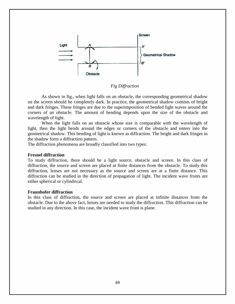
69
Fig Diffraction
As shown in fig., when light falls on an obstacle, the corresponding geometrical shadow
on the screen should be completely dark. In practice, the geometrical shadow consists of bright
and dark fringes. These fringes are due to the superimposition of bended light waves around the
corners of an obstacle. The amount of bending depends upon the size of the obstacle and
wavelength of light.
When the light falls on an obstacle whose size is comparable with the wavelength of
light, then the light bends around the edges or corners of the obstacle and enters into the
geometrical shadow. This bending of light is known as diffraction. The bright and dark fringes in
the shadow form a diffraction pattern.
The diffraction phenomena are broadly classified into two types:
Fresnel diffraction
To study diffraction, there should be a light source, obstacle and screen. In this class of
diffraction, the source and screen are placed at finite distances from the obstacle. To study this
diffraction, lenses are not necessary as the source and screen are at a finite distance. This
diffraction can be studied in the direction of propagation of light. The incident wave fronts are
either spherical or cylindrical.
Fraunhofer diffraction
In this class of diffraction, the source and screen are placed at infinite distances from the
obstacle. Due to the above fact, lenses are needed to study the diffraction. This diffraction can be
studied in any direction. In this case, the incident wave front is plane.

70
Fraunhofer Diffraction at Single Slit
Fig. 1 Fraunhofer diffraction at single slit
Consider the width of the slit AB is equal to “e”. Let a plane wave front WWʹ of monochromatic
light of wavelength λ propagating normally towards the slit is incident on the slit AB. The
diffracted light through the slit is focused by means of a convex lens on a screen placed in the
focal plane of the lens. Every point on the wave front in the slit will act as a source of secondary
wavelets. The secondary wavelets travelling in the direction of OPo are brought to focus at Po on
the screen SSʹ by using a converging lens L. The secondary wavelets from AB which are brought
to focus at Po have no path difference. Hence the intensity at Po is high and it isknown as central
maximum. The secondary wavelets in the slit AB which make an angle „θ‟ with OPo direction are
brought to a point P1 on the screen.
Intensity at point P1 depends on the path difference between the wavelets at A and at B
reaching to point P1. To find the path difference, a perpendicular AC is drawn to BR form A.
Now the path difference between the secondary wavelets from A and B in the direction of OP1 is
BC.

71
Path difference = BC = AB sin = e sinθ
corresponding phase difference = 2𝜋
𝜆 x path difference =
2𝜋
𝜆 xe sinθ
Let the width of the slit be divided into „n‟ equal parts and the amplitude of the wave from each
part is „a‟. The phase difference between any two successive waves from these parts would be
1
𝑛 [total phase] =
1
𝑛 [
2𝜋
𝜆 e sinθ] = d (say)
Using the method of vector addition of amplitudes, the resultant amplitude R is given by
R = 𝑎 sin 𝑛𝑑 /2
sin 𝑑/2
= 𝑎𝑠𝑖𝑛 (𝜋𝑒 sin
𝜃
𝜆)
𝑆𝑖𝑛 (𝜋𝑒 sin𝜃
𝑛𝜆
= a sin 𝛼
sin 𝛼/𝑛
= na sin 𝛼
𝛼 (i.e. na = A)
R = A sin 𝛼
𝛼
Intensity = I = R= A2 (
sin 𝛼
𝛼)2
………………… (1)
Principal maximum:
The resultant amplitude R can be written in ascending powers of α as
R = A[ α - α2
3!+
α4
5!−
α6
7! + …]
I will be maximum, when the value of R is maximum. For maximum value of R, the negative
terms must vanish, i.e., α = 0
𝜋𝑒 sin 𝜃
𝜆= 0
sin θ = 0
θ = 0 ………………… (2)
Then, R = A
Imax = R2 = A
2 ………………… (3)
The condition θ = 0 means that the maximum intensity is formed at Po and is known as principal
maximum.

72
Minimum Intensity
I will be minimum, when sin α = 0
α = ± π, ± 2π, ± 3π
α = ± mπ 𝜋𝑒 sin 𝜃
𝜆= ± mπ
e sinθ = ± mλ…………… (4)
where m = 1, 2, 3, …
Thus, we obtain the points of minimum intensity on either side of the principal maximum. For m
= 0, sinθ = 0, which corresponds to principal maximum.
Secondary maxima:
In between the minima, we get secondary maxima. The positions can be obtained by
differentiating the expression of I w.r.t. α and equating to zero. We get
𝑑𝐼
𝑑𝛼=
𝑑
𝑑𝛼 [ A
2 (
sin 𝛼
𝛼)2] = 0
A2[
2sin 𝛼
𝛼. αcos α −𝑠𝑖𝑛𝛼
α2 ] = 0
Either sin α = 0 or αcos α – sin α = 0
sin α = 0 gives positions of minima.
Hence the positions of secondary maxima are given by α cos α – sin α = 0
α = tan α ………………… (5)
The values of α satisfying the above equation are obtained graphically by plotting the curves y =
α and y = tan α on the same graph. The points of intersection of the two curves gives the values
of α which satisfy the above equation. The plots of y = α and y = tan α are shown in Fig. 2

73
Fig. 2 Plots of y = α and y = tan α
The points of intersections are α = 0, ± 3𝜋
2 , ±
5𝜋
2, …..
substituting the above values in equation (1), we get the intensities in various maxima.
α = 0, Io = A2
(Principal maximum)
α = 3𝜋
2, Io = A
2 [
sin 3𝜋/2
3𝜋/2 ]
2 ≈
A2
22(1
st secondary maximum)
α = 5𝜋
2, Io = A
2 [ ] ≈
A2
62(2
nd secondary maximum)
Fig. 3 Intensity distribution of diffraction due to single slit
Fraunhofer Diffraction at Double Slit
Let S1 and S2 be double slits of equal widths e and separated by a distance d. The distance
between the middle points of the two slits is (e +d). A monochromatic light of wave length λ is
incident normally on the two slits. The light diffracted from these slits is focused by a lens on the
screen placed in the focal plane of the lens. The diffraction at two slits is the combination of
diffraction as well as interference, i.e., the pattern on the screen is the diffraction pattern due to a
single slit on which a system of interference fringes is superimposed. When a plane wave front is
incident normally on two slits, the secondary wavelets from the slits travel uniformly in all
directions. The wavelets travelling in the direction of incident light come to a focus at 𝑃0 while
the wavelets travelling in a direction making an angle𝜃, come to focus at 𝑃1.
Fraunhofer diffraction-double slit

74
From the study of diffraction due to single slit, the resultant amplitude = 𝐴 sin 𝛼
𝛼
Where,
𝛼 = 𝜋𝑒 𝑠𝑖𝑛𝜃
𝜆.
Since a double slit is used, from each slit a wavelet of amplitude 𝐴 sin 𝛼
𝛼 in a
directionθ is obtained. These two wavelets interfere and meet at a point 𝑃1 on the screen. To
calculate the path difference between the wavelets, draw a normal 𝑆1𝐾 to the wavelet through𝑆2.
Path difference = 𝑆2𝐾
= 𝑒 + 𝑑 sin 𝜃
Phase difference 𝛿 = 2𝜋
𝜆 𝑒 + 𝑑 sin 𝜃 →(6)
Vector addition method
To find the resultant amplitude at 𝑃1vector addition method is used. (Fig. 7.12) in which the two
sides of a triangle are represented by the amplitudes through 𝑆1 and 𝑆2. The third side gives the
resultant amplitude.
From the figure,
𝑂𝐻 2 = 𝑂𝐺 2 + 𝐺𝐻 2 + 2 𝑂𝐺 𝐺𝐻 𝑐𝑜𝑠𝛿
𝑅2 = 𝐴 sin 𝛼
𝛼
2
+ 𝐴 sin 𝛼
𝛼
2
+ 2 𝐴𝑠𝑖𝑛 𝛼
𝛼
𝐴𝑠𝑖𝑛 𝛼
𝛼 𝑐𝑜𝑠𝛿
= 𝐴2 𝑠𝑖𝑛2𝛼
𝛼[2+2𝑐𝑜𝑠𝛿]
= 2 𝐴𝑠𝑖𝑛𝛼
𝛼
2 1 + 𝑐𝑜𝑠𝛿
= 2 𝐴𝑠𝑖𝑛𝛼
𝛼
2 1 + 2𝑐𝑜𝑠2 𝛿 2 − 1
= 4 𝐴𝑠𝑖𝑛𝛼
𝛼
2
𝑐𝑜𝑠2 𝛿 2
𝑅2 = 4𝐴2 𝑠𝑖𝑛𝛼
𝛼
2
𝑐𝑜𝑠2 𝜋 𝑒+𝑑 𝑠𝑖𝑛𝜃
𝜆
Let 𝛽 = 𝜋 𝑒+𝑑 𝑠𝑖𝑛𝜃
𝜆
𝑅2 = 4𝐴2 𝑠𝑖𝑛𝛼
𝛼
2
𝑐𝑜𝑠2𝛽
The resultant intensity I = 𝑅2 = 4𝐴2 𝑠𝑖𝑛𝛼
𝛼
2
𝑐𝑜𝑠2𝛽 → (7)

75
From the above expression, it is clear that the resultant intensity is the product of two factors, i.e,
1. 𝐴2 𝑠𝑖𝑛𝛼
𝛼
2
which represents the diffraction pattern due to a single slit
2. 𝑐𝑜𝑠2𝛽, which gives the interference pattern due to wavelets from double slits. The resultant
intensity is due to both diffraction and interference effects.
Diffraction Effect
The diffraction term 𝐴2 𝑠𝑖𝑛𝛼
𝛼
2
gives the principal maximum as the centre of the
screen with alternate minima and secondary maxima of decreasing intensity. We get
principal maximum for 𝜃 = 0. We get minima for 𝑠𝑖𝑛𝛼 = 0
𝛼 =±𝑚𝜋, where m = 1, 2, 3…
𝜋𝑒 𝑠𝑖𝑛𝜃
𝜆 = ±𝑚𝜋
𝑒 𝑠𝑖𝑛𝛳 = ±𝑚𝜆
The positions of secondary maxima occur for
𝛼 =±3𝜋
2 ,
±5𝜋
2 ,
±7𝜋
2 …..
Interference Effect
The interference term cos2β gives the equidistant bright and dark fringes.
The maxima will occur for cos2β = 1
β =±𝑛𝜋, where n = 0, 1, 2, 3…
β = 0, ± π, ± 2π, ± 3π…………
𝜋 𝑒+𝑑 𝑠𝑖𝑛𝛳
𝜆 = ±nπ
𝑒 + 𝑑 𝑠𝑖𝑛𝛳 = ±𝑛𝜆
The minima will occur for cos2β =0
β =± 2𝑛 + 1 𝜋
2 𝑤𝑒𝑟𝑒 𝑛 =0, 1, 2, 3…
(e+d) sin𝛳 = ±(2𝑛 + 1)𝜆
2

76
Intensity Distribution
Figure 7.13 (a) and (b) represents the intensity variations due to diffractions as well as
interference effect individually. When both effects are combined then the resultant intensity
variation is obtained. From the figure it is clear that the resultant minima are not equal to zero,
still they have some minimum intensity due to interference effect.
(a) Diffraction effect (b) Interference effect (c) Resultant intensity
4. Discuss the Fraunhofer diffraction due to a N-slits and obtain the intensity distribution
and positions of maxima and minima.
(or)
Give the construction and theory of a plane diffraction grating of the transmission type and
explain the formation of spectra by it.
Ans.
Construction:
An arrangement which consists of a large number of parallel slits of the same width and
separated by equal opaque spaces is known as diffraction grating. Fraunhofer used the first
grating consisting of a large number of parallel wires placed side by side very closely side by
side at regular intervals. The diameters of the wires were of the order of 0.05 mm diameter and
their spacing, varied from 0.0533 mm to 0.687 mm. Now gratings are constructed by ruling
equidistant parallel lines on a transparent material such as glass, with a fine diamond point.
Usually 15,000 lines are drawn on one-inch width of the grating. The ruled lines are opaque to
light while the space between any two lines is transparent to light and acts as a slit. This is
known as plane transmission grating.

77
Theory:
Fig. 1 Diffraction grating
Fig. 1, represents the section of a plane transmission grating placed perpendicular to the
plane of the paper. Let „e‟ be the width of each slit and these slits are separated by equal opaque
regions part of each width „d‟. Then (e +d) is known as grating element. XY is the screen placed
perpendicular to the plane of a paper. Suppose a parallel beam of monochromatic light of
wavelength λ be incident normally on the grating. By Huygen‟s principle, each of the slit sends
secondary wavelets in all directions. The secondary wavelets travelling in the same direction of
incident light will come to a focus at a point P1 of the screen as the screen is placed at the focal
plane of the convex lens. The point Po will be a central maximum. Now consider the secondary
waves travelling in a direction inclined at an angle θ with the direction of the incident light.
These waves reach point P1 on passing through the convex lens in different phases. As a result,
dark and bright bands on both sides of central maximum are obtained.
The intensity at point P1 may be considered by applying the theory of Fraunhofer
diffraction at a single slit. The resultant amplitude due to diffraction at single slit is 𝐴 sin 𝛼
𝛼 ,
which is now at the middle point of each slit where, α = πe sinθ/λ. Let us assume that there are N
slits on the grating. The path difference between the corresponding points is (e + d) sin θ and in
terms of phase difference it is 2𝜋
𝜆(e + b) sinθ = 2β. The resultant of N amplitudes, each of
𝐴 sin 𝛼
𝛼
with common phase difference (2β) between consecutive diffracted amplitudes can be obtained
by the vector addition method. The resultant amplitude (R) of the N amplitudes each of 𝐴 sin 𝛼
𝛼 is
R = 𝐴 sin 𝛼
𝛼 .
sin 𝑁𝛽
sin 𝛽 (1)
and intensity I = R2 =
𝐴 sin 𝛼
𝛼 2(
sin 𝑁𝛽
sin 𝛽 ) 2
(2)

78
The value 𝐴 sin 𝛼
𝛼 2
shows the intensity distribution due to single slit diffraction and sin2Nβ/sin
2β
shows the combined intensity distribution due interference at all the N slits.
Discussion of intensity distribution:
Principal maxima:
From equation (2), we know that the intensity would be maximum when sin β = 0, where β = 0,
π, 2π, 3π, …. = nπ and n = 0,1,2, 3, ...
Then sin 𝑁𝛽
sin 𝛽 =
0
0
The above factor is indeterminate; To find its value, the numerator and denominator are
differentiated separately. i.e., by applying the Hospital‟s rule. Thus
Fig. 2

79
Fig. 3(a) the variation of intensity due to the factor sin2 α/α
2 is represented; (b) the variation of
intensity due to the factor sin2 Nβ/sin
2β is represented and (c) the resultant variation of intensity
is represented.
Diffraction Grating
An arrangement which consists of a large number of parallel slits of the same width and
separated by equal opaque spaces is known as diffraction grating. Fraunhofer used the first
grating consisting of a large number of parallel wires placed side by side very closely at regular
intervals. Now gratings are constructed by ruling equidistant parallel lines on a transparent
material such as glass with a fine diamond point. The ruled lines are opaque to light while the
space between any two lines is transparent to light and acts as a slit.
Commercial gratings are produced by taking the cast of an actual grating on a transparent film
like that of cellulose acetate. Solution of cellulose acetate is poured on the ruled surface and
allowed to dry to form a thin film, detachable from the surface. These impressions of a grating
are preserved by mounting the film between two glass sheets.
Fig7.17 Diffraction Grating
Let „e‟ be the width of the line and „d‟ be the width of the slit. Then (e+d) is known as grating
element. If „N‟ is the number of lines per inch on the grating, then
N (e+d) =1” =2.54 cm
e+d= 2.54
𝑁 cm
There will be nearly 30,000 lines per inch of a grating. Due to the above fact, the width of the
slit is very narrow and is comparable to the wavelength of light. When light falls on the grating,
the light gets diffracted through each slit. As a result, both diffraction and interference of
diffracted light gets enhanced and forms a diffraction pattern. This pattern is known as
diffraction spectrum.
Grating Spectrum
The condition to form the principal maxima in a grating is given by
(e+d) sin Ѳ = nλ
Where (e+d) is the grating element and the above equation is known as grating equation.

80
From the grating equation, the following is clear.
1. For a particular wavelength λ, the angle of diffraction Ѳ is different for principal maxima
of different orders.
2. As the number of lines in the grating is large, maxima appear as sharp, bright parallel
lines and are termed as spectral lines.
3. For white light and for a particular order of n, the light of different wavelengths will be
diffracted in different directions.
4. At the center, Ѳ=0 gives the maxima of all wavelengths which coincides to form the
central image of the same color as that of the light source. This forms zero order.
(Fig.2.9)
5. The principal maxima of all wavelengths forms the first, second, order spectra for n=1,2,
…
6. The longer the wavelength, greater is the angle of diffraction. Thus, the spectrum consists
of violet being in the innermost position and red being in the outermost positions.
Fig7.18 Grating Spectrum
7. Most of the intensity goes to zero order and the rest is distributed among other orders.
8. Spectra of different orders are situated symmetrically on both sides of zero order.
9. The maximum number of orders available with the grating is nmax= 𝑒+𝑑
𝜆
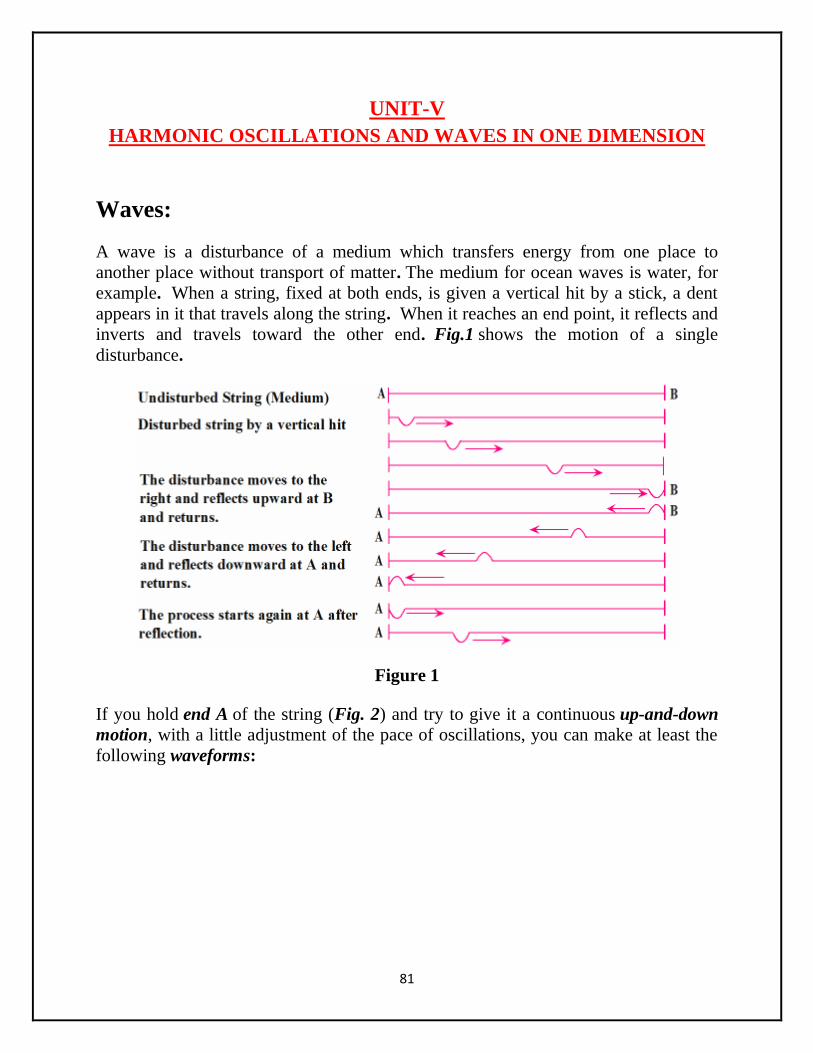
81
UNIT-V
HARMONIC OSCILLATIONS AND WAVES IN ONE DIMENSION
Waves:
A wave is a disturbance of a medium which transfers energy from one place to
another place without transport of matter. The medium for ocean waves is water, for
example. When a string, fixed at both ends, is given a vertical hit by a stick, a dent
appears in it that travels along the string. When it reaches an end point, it reflects and
inverts and travels toward the other end. Fig.1 shows the motion of a single
disturbance.
Figure 1
If you hold end A of the string (Fig. 2) and try to give it a continuous up-and-down
motion, with a little adjustment of the pace of oscillations, you can make at least the
following waveforms:

82
Figure 2
Each wave travels from A to B and reflects at B. When each reflected wave reaches
point A, it reflects again and the process repeats. Of course, the up and down motion
of hand keeps putting energy into the system by constantly generating waves that are
in phase with the returned waves creating the above waveforms. Although the waves
appear to be standing as they are called "standing waves," they are actually traveling
back-and-forth along the string. The subject of waves is lengthy, complicated, and
mathematically very involved. The above is enough to give you an idea.
Types of Waves:
There are two classifications: one classification of waves
is: mechanical and electromagnetic.
Mechanical waves require matter for their transmission. Sound waves, ocean waves,
and waves on a guitar string are examples. Air, water, and metal string are their
media (matter), respectively.
Electromagnetic waves travel both in vacuum and matter. If light (an
electromagnetic wave itself) could not travel in vacuum, we would not see the Sun.
Radio waves, ultraviolet waves, and infrared waves are all electromagnetic waves and
travel in vacuum.
Waves are also classified as transverse and longitudinal (See Fig. 3).
For a transverse wave the disturbance direction is perpendicular to
the propagation direction. Water waves are transverse. Waves on guitar strings are
also transverse.

83
For a longitudinal wave the disturbance direction is parallel to
the propagation direction. Waves on a slinky as well as sound waves are
longitudinal.
Figure 3
Frequency ( f ):
The frequency f of a wave is the number of full waveforms generated per second.
This is the same as the number of repetitions per second or the number of oscillations
per second. The SI unit for frequency is (1/s), or (s-1), called "Hertz (Hz)."
Period ( T ):
Period T is the number of seconds per waveform, or the number of seconds per
oscillation. It is clear that frequency and period are reciprocals.
T = 1/f
Also, recall the useful relation between frequency f and the angular speed ω :
ω = 2π f.

84
ω is the number of radians per second, but f is the number of turns or oscillations
per second. Each turn is 2π radians.
Wavelength ( λ ):
Wavelength λ is the distance between two successive points on a wave that are in the
same state of oscillation. Points A and B in Fig. 4 are the nearest or successive points
that are both the same amount passed the maximum and therefore in the same state of
oscillation.
Figure 4
Wavelength may also be defined as the distance between a peak to the next, or the
distance between a trough to the next, as shown above.
Also pay attention to Fig. 5. It shows that the distance between any node and the
anti-node next to it is λ/4.
Figure 5
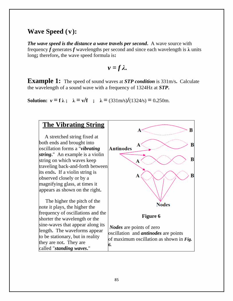
85
Wave Speed ( v ):
The wave speed is the distance a wave travels per second. A wave source with
frequency f generates f wavelengths per second and since each wavelength is λ units
long; therefore, the wave speed formula is:
v = f λ.
Example 1: The speed of sound waves at STP condition is 331m/s. Calculate
the wavelength of a sound wave with a frequency of 1324Hz at STP.
Solution: v = f λ ; λ = v/f ; λ = (331m/s)/(1324/s) = 0.250m.
The Vibrating String
A stretched string fixed at
both ends and brought into
oscillation forms a "vibrating
string." An example is a violin
string on which waves keep
traveling back-and-forth between
its ends. If a violin string is
observed closely or by a
magnifying glass, at times it
appears as shown on the right.
The higher the pitch of the
note it plays, the higher the
frequency of oscillations and the
shorter the wavelength or the
sine-waves that appear along its
length. The waveforms appear
to be stationary, but in reality
they are not. They are
called "standing waves."
Figure 6
Nodes are points of zero
oscillation and antinodes are points
of maximum oscillation as shown in Fig.
6.

86
Now, look at the following example:
Example 2: In a 60.0-cm long violin
string, three antinodes are observed. Find
the wavelength of the waves on it.
Solution: Each loop has a length of
60.0cm /3 = 20.0cm.
Each wavelength (a full sine wave)
contains two of such loops; therefore,
Fig. 7
λ = 40.0cm.
Speed of Waves in a Stretched String:
The speed of waves in a stretched
string depends on the tension F in
the string as well as the mass per
unit length μ of the string as
explained below:
The more a string is stretched, the
faster waves travel in it.
The formula that relates tension F in
the string and the waves speed v is:
Proof:
If we model the peak of a wave as it passes through the medium (the string) at
speed v as shown in Fig. 8, we may think that the peak segment is under a tensile
force F that pulls it in opposite directions.The hump can be looked at as a portion of a
circle from A to B with its center at C. The hump is being pulled down by a force
of magnitude 2Fsin . This pulling down force passes through the center and
therefore acts as a centripetal force for the segment that is equal
to Mv2/R ; therefore, 2Fsin = Mv2/R. For small angles and in
radians, sin = . The formula becomes:
2F = Mv2/R (1) where M = the mass of the string segment.

87
If we calculate mass M of the
hump, it results
in M = 2μRθ.
This is because the length of the
hump is 2Rθ and μ is the mass
per unit length of the string. In
other words,
μ= mass /length. Eqn.
(1) takes the form:
2F = 2μRθ v2/R (2)
Solving for v results in:
Figure 8
Example : A 120-cm guitar string is under a tension of 400N. The mass of the
string is 0.480 grams. Calculate (a) the mass per unit length of the string and (b) the
speed of waves in it. (c) In a diagram show the number of (1/2)λ's that appear in this
string if it is oscillating at a frequency of 2083Hz.
Solution: (a) μ = M/L ; μ = 0.480x10⁻³kg/1.20m = 4.00x10
-4 kg/m.
(b) v = (F/μ)1/2 ; v = [400N/4.00x10-4kg/m]1/2 = 1000 m/s.
(c) v = f λ ; λ = v/f ; λ = (1000m/s)/(2083/s) = 0.480m.
(1/2)λ = 0.480m/2 = 0.240m.
The number of (λ/2)'s that fit in this string length of 120cm is
1.20m/0.240m = 5.00, as shown in Fig. 8.

88
Figure 9
Traveling Harmonic Waves:
We are interested in finding a formula that calculates the y-value at any point in a one
dimensional medium as harmonic waves travel in it at speed v. This means that at
any point x and at any instant t, we want y(x,t). For harmonic waves, such equation
has the general form:
y(x,t) = A sin(kx - ωt + φ)
k is called the wave number and its unit in SI is m-1. The above equation is for one
dimensional harmonic waves traveling along the +x axis. If the waves are moving
along the -x axis, the appropriate equation is:
y(x,t) = A sin(kx + ωt + φ).
If y = 0 at t = 0 and x = 0, then φ = 0. It is important to distinguish between the
wave propagation velocity v (along the x-axis) and the medium's particles
velocity vy (along the y-axis) as transverse waves pass by the particles of the
medium. The wave propagation velocity is V = f λ , but the particles velocity in the
y-direction is vy = ∂y/∂t. The symbol "∂ " denotes "partial derivative."

89
Example : The equation of certain traveling waves is
y(x,t) = 0.0450 sin(25.12x - 37.68t - 0.523)
where x and y are in meters, and t in seconds. Determine the following: (a)
Amplitude, (b) wave number, (c) wavelength, (d) angular frequency, (e) frequency, (f)
phase angle, (g) the wave propagation speed, (h) the expression for the medium's
particles velocity as the waves pass by them, and (i) the velocity of a particle that is
at x = 3.50m from the origin at t = 21.0s.
Solution: Comparing this equation with the general form, results in
(a) A = 0.0450m ; (b) k = 25.12m-1 ; (c) λ = (2π/k) = 0.250m
(d) ω = 37.68rd/s ; (e) f = ω/(2π) = 6.00Hz ; (f) φ = -0.523 rd ;
(g) v = f λ =1.50m/s; (h) vy = ∂y/∂t = 0.045(-37.68) cos (25.12x - 37.68t - 0.523)
(i) vy(3.5m, 21s) = 0.045(-37.68) cos (25.12*3.5-37.68*21-0.523) = -1.67m/s.
Standing Harmonic Waves:
When two harmonic waves of equal frequency and amplitude travel through a
medium in opposite directions, they combine and the result can form standing waves.
If the equation of the wave going to the right is y1 = A sin(kx - ωt) and that of the one
going to the left is y2 = A sin(kx + ωt), we may add the two to obtain the equation of
the combination wave as
y(x,t) = Asin(kx - ωt) + A sin(kx + ωt)
Using the trigonometric identity: sin a + sin b = 2sin[(a + b)/2] cos [(a - b)/2],
we get: y(x,t) = 2Acos(ωt) ∙ sin(kx).
In this equation, sin(kx) determines the shape of the standing wave and
2Acos(ωt) determines how its amplitude varies with time.

90
If at t = 0, the red wave that is going
to the right is in phase with the blue
wave that is going to the left, they
add up constructively and
the amplitude of the sum (the
gray) is twice each amplitude as
shown at t = 0.
At t = T/4 the become completely out
of phase and cancel each others effect
to a sum of zero. This is only for a
very brief instant (the gray becomes a
straight line).
At t = T/2, the opposite of t = 0
occurs. The two humps become
troughs and the single trough
becomes s hump.
In another half a period the shape of
the gray (or the sum) become like the
one at t = 0.
Confirm the above explanation by
looking at the different figures shown
on the right (Fig. 10).
I
Figure 10
Resonant Standing Waves in A String:
In a medium with limited boundary such as a string fixed at both ends, standing waves
can only be formed for a set of discrete frequencies or wavelengths.
If you hold one end of a rope, say 19ft long, and tie the other end of it to a wall 16ft
away from you, there will be a slack of 3ft in it allowing you to swing it up and down
and make waves. By adjusting the frequency of the oscillatory motion you give to the

91
end you are holding, you can generate a sequence of waves in the rope that will have
an integer number of loops in it. For a frequency f, there is a corresponding
wavelength λ such that V = f λ .
It is very clear from this equation that, since
the waves speed, V , in a given medium is
constant, the product f λ is also constant.
This means that if you increase frequency f,
the wavelength λ of the waves in the rope has
to decrease.
Of course, for resonance, the values of such
frequencies, as was mentioned, are discrete,
and so are their corresponding wavelengths.
All you need to do is to adjust your hand's
oscillations for each case to observe a full
number of loops in the rope between you and
the wall. It is also clear from Example
2 that each loop is one half of the
wavelength in each case. When the entire
length of the rope accommodates one loop
only, it is called the fundamental
frequency and that is the lowest possible
frequency.
The subsequent 2-loop, 3-loop, 4-loop, and
... cases are called the 2nd, 3rd, 4th, and ....
harmonics of that fundamental frequency as
shown on the right (Fig. 11).
Figure 11
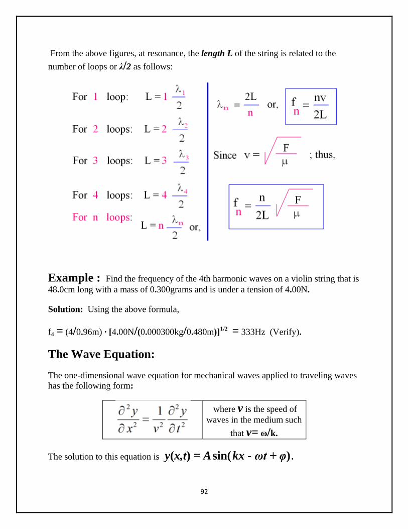
92
From the above figures, at resonance, the length L of the string is related to the
number of loops or λ/2 as follows:
Example : Find the frequency of the 4th harmonic waves on a violin string that is
48.0cm long with a mass of 0.300grams and is under a tension of 4.00N.
Solution: Using the above formula,
f4 = (4/0.96m) ∙ [4.00N/(0.000300kg/0.480m)]1/2 = 333Hz (Verify).
The Wave Equation:
The one-dimensional wave equation for mechanical waves applied to traveling waves
has the following form:
where v is the speed of
waves in the medium such
that v= ω/k.
The solution to this equation is y(x,t) = A sin( kx - ωt + φ) .

93
Example : Show that the equation y(x,t) = A sin(kx - ωt + φ) satisfies the wave
equation.
Solution: Take the appropriate partial derivatives and verify by substitution.
Energy Transport on a String:
As a wave travels along a string, it transports energy by being flexed point by point,
or dx by dx. By dx , we mean differential length. It is easy to calculate
the K.E. and P.E. of a differential element as shown in Fig. 12. Let dl be a
differential segment of the string. Corresponding to this dl , there is a dx and a dy as
shown.
Note that dl is a stretched dx but has the same mass as dx.

94

95
The conclusion is that the power transmission by a wave on a string is proportional
to the squares of angular speed and amplitude and linearly proportional to the wave
speed V in the string.
Example : A 1.00m-long string has a mass of 2.5 grams and is forced to oscillate
at 400Hz while under a tensile force of 49N. If the maximum displacement of the
string in the direction perpendicular to the waves propagation is 8.00mm, find its
average power transmission.
Solution: We need to apply the formula Pavg = 0.5μ(ωA)2v.
First μ = M/L, ω = 2πf, A, and V = (F/μ)0.5 must be calculated.
μ = 2.5x10⁻³ kg/m, ω = 2512 rd/s, V = 140. m/s, A = 4.00x10
-3m , and
finally, Pavg = 17.7 watts. Verify all calculations.