vol. 5, issue 3, march 2016 modified upqc for compensation ... · keywords: facts, sssc,svc, ipfc,...
TRANSCRIPT
ISSN(Online) : 2319-8753 ISSN (Print) : 2347-6710
International Journal of Innovative Research in Science, Engineering and Technology
(An ISO 3297: 2007 Certified Organization)
Vol. 5, Issue 3, March 2016
Copyright to IJIRSET DOI:10.15680/IJIRSET.2016.0503210 3659
Modified UPQC for Compensation Power Quality Problems Using MLI with Modified
PWM Method
Elavarasan P1, Sathyamurthy K2 PG Scholar, Dept of EEE, Arignar Anna Institute of Science and Technology, Chennai, India1
Assistant Professor, Dept of EEE, Arignar Anna Institute of Science and Technology, Chennai, India2
ABSTRACT: The unified power quality conditioner (UPQC) is a custom power device, which mitigates voltage and current-related PQ issues in the power distribution systems. In this project, a UPQC topology for applications with non-stiff source is proposed. The proposed topology enables UPQC to have a reduced harmonics. In this project the unified power quality conditioner (UPQC) deals with a solution to compensate the voltage sags and swells and to protect sensitive load In order to apply the MLI in the distribution systems with voltage in range of kilovolts, series converter as one of the important components of UPQC should be implemented based on the multilevel converters which have the capability to handle voltage in the range of kilovolts and power of several megawatts. So, in this project a configuration of UPQC based on asymmetrical cascade Multicell converter is proposed. The main property of this asymmetrical CM converter is increase in the number of output voltage levels with reduced number of switches. Also, the pre-sag compensation strategy and the proposed voltage sag/swell detection .
KEYWORDS: FACTS, SSSC,SVC, IPFC, CSC, UPFC, UPQC, STATCOM.
I. INTRODUCTION
With the advancement of power electronics and digital control technology, the renewable energy the proliferation of the power electronics devices, nonlinear loads and unbalanced loads have degraded the power quality (PQ) in the power distribution network. Custom power devices have been proposed for enhancing the quality and reliability of electrical power. Unified PQ conditioner (UPQC) is a versatile custom power device which consists of two inverters connected back-to-back and deals with both load current and supply voltage imperfections. UPQC can simultaneously act as shunt and series active power filters. The series part of the UPQC is known as dynamic voltage restorer (UPQC 15 MLI). It is used to maintain balanced, distortion free nominal voltage at the load. The shunt part of the UPQC is known as distribution static compensator (DSTATCOM), and it is used to compensate load reactive power, harmonics and balance the load currents thereby making the source current balanced and distortion free with unity power factor.Voltage rating of dc-link capacitor largely influences the compensation performance of an active filter. In general, the dc-link voltage for the shunt active filter has much higher value than the peak value of the line-to-neutral voltage. This is done in order to ensure a proper compensation at the peak of the source voltage. The authors mentioned about the current distortion limit and loss of control limit, which states that the dc-link voltage should be greater than or equal to √6 times the phase voltage of the system for distortion-free compensation. Due to the aforementioned criteria, many researchers have used a higher value of dc capacitor voltage based on applications Similarly, for series active filter, the dc-link voltage is maintained at a value equal to the peak of the line-to-line voltage of the system for proper compensation .To reduce the dc-link voltage storage capacity, few attempts were made in literature. A hybrid filter has been discussed for motor drive applications. The filter is connected in parallel with diode rectifier and tuned at seventh harmonic frequency. Although an elegant work, the design is specific to the motor drive application, and the reactive power compensation is not considered, which is an important aspect in UPQC applications. In case of the three-phase four-wire system, neutral-clamped topology is used for UPQC. This topology enables the independent control of each leg of both the shunt and series inverters, but it requires capacitor voltage balancing. Four-leg VSI topology for shunt active filter has been proposed for three-phase four-wire system. This
ISSN(Online) : 2319-8753 ISSN (Print) : 2347-6710
International Journal of Innovative Research in Science, Engineering and Technology
(An ISO 3297: 2007 Certified Organization)
Vol. 5, Issue 3, March 2016
Copyright to IJIRSET DOI:10.15680/IJIRSET.2016.0503210 3660
topology avoids the voltage balancing of the capacitor, but the independent control of the inverter legs is not possible. To overcome the problems associated with the four-leg topology, the authors proposed a T-connected transformer and three-phase VSC-based DSTATCOM. However, this topology increases the cost and bulkiness of the UPQC because of the presence of extra transformer. In conventional 11 levels multi-level inverter is implemented but harmonics is injected. So, we have implement 15 level in proposed system.
II.LITERATURE SURVEY
The unified power quality conditioner (UPQC) is a custom power device, which mitigates voltage and current-related PQ issues in the power distribution systems. In this project, a UPQC 15 level MLI topology for applications with non-stiff source. This project deals with a dynamic voltage restorer (UPQC 15 MLI) as a Solution to compensate the voltage sags and swells and to protect sensitive loads. Multilevel converters are very interesting alternatives for medium and high-power applications. Here we developed an improved configuration of double flying capacitor Multicell (DFCM) converter. The benefits of this new converter comparing with conventional DFCM, are doubling of the number of output voltage levels and improving the output voltage frequency spectrum.Multilevel converters are very interesting alternatives for medium and high-power applications. Here we developed an improved configuration of double flying capacitor Multicell (DFCM) converter. The benefits of this new converter comparing with conventional DFCM, are doubling of the number of output voltage levels and improving the output voltage frequency spectrum.
III. PROJECT DESCRIPTION
To reduce harmonics of circuit, we have implemented 15 level MLI is applied.
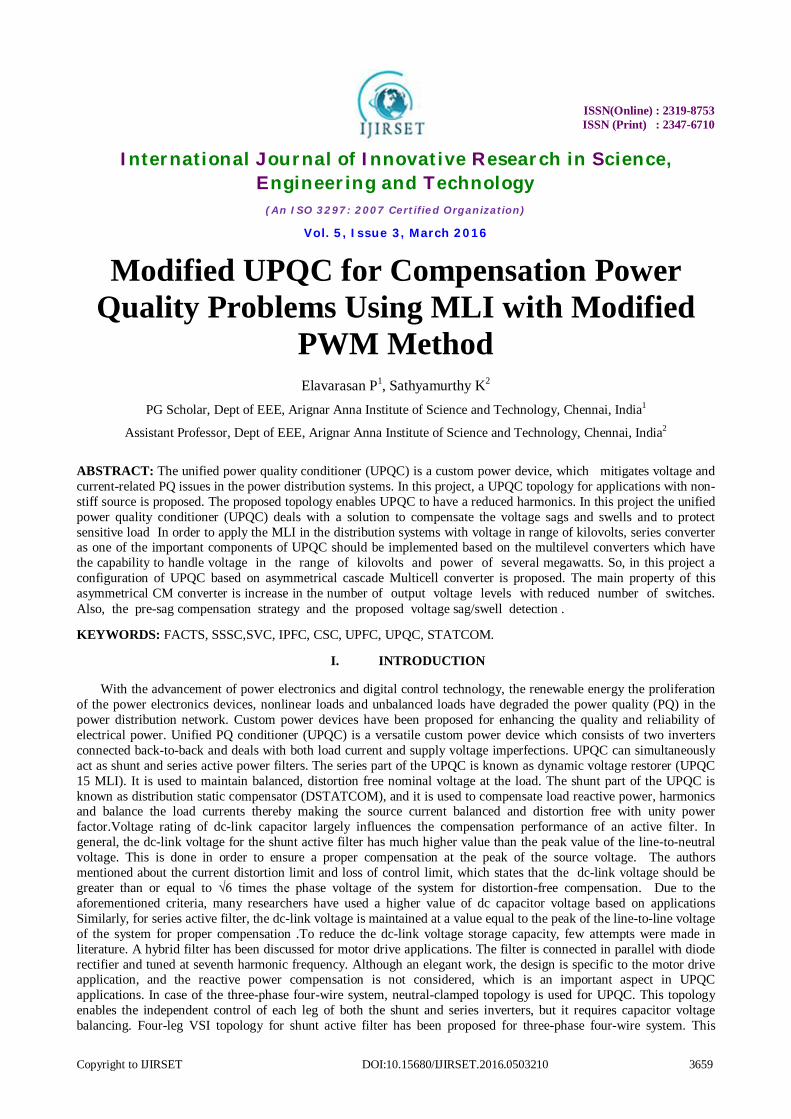
Fig. 1 Normal Pwm method with 8 switches for 11 level inverter
PROPOSED SYSTEM
1. Modified Pwm method with 10 switches for 15 level inverter.
2.15 level inverter injecting UPQC devices or Statcom for compensation power quality problems.
ISSN(Online) : 2319-8753 ISSN (Print) : 2347-6710
International Journal of Innovative Research in Science, Engineering and Technology
(An ISO 3297: 2007 Certified Organization)
Vol. 5, Issue 3, March 2016
Copyright to IJIRSET DOI:10.15680/IJIRSET.2016.0503210 3661
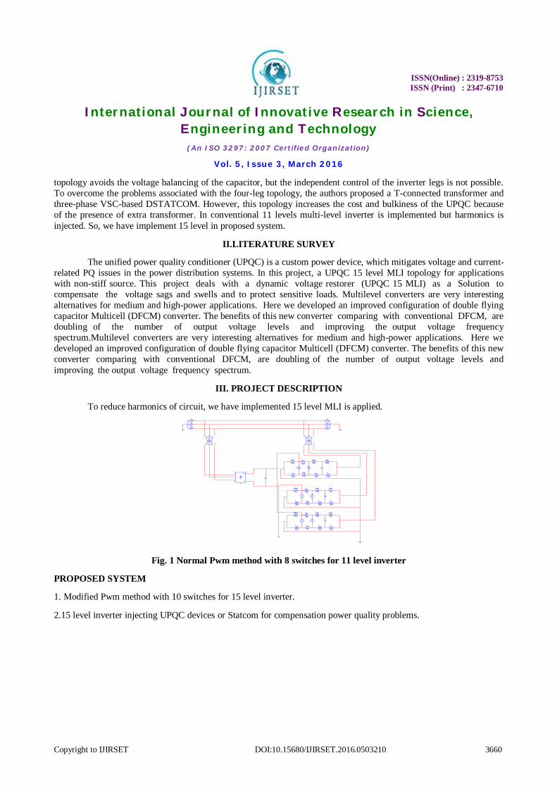
Fig 2 Block diagram
A Unified Power Quality Conditioner (UPQC) is a device that is similar in construction to a Unified Power Flow Conditioner (UPFC). The UPQC, just as in a UPFC, employs two voltage source inverters (VSIs) that connected to a D.C. energy storage capacitor. One of these two VSIs is connected in series with A.C. line while the other is connected in shunt with the A.C. system.
A UPQC that combines the operations of a Distribution Static Compensator (DSTATCOM) and Dynamic Voltage Regulator (UPQC 15 MLI) together.
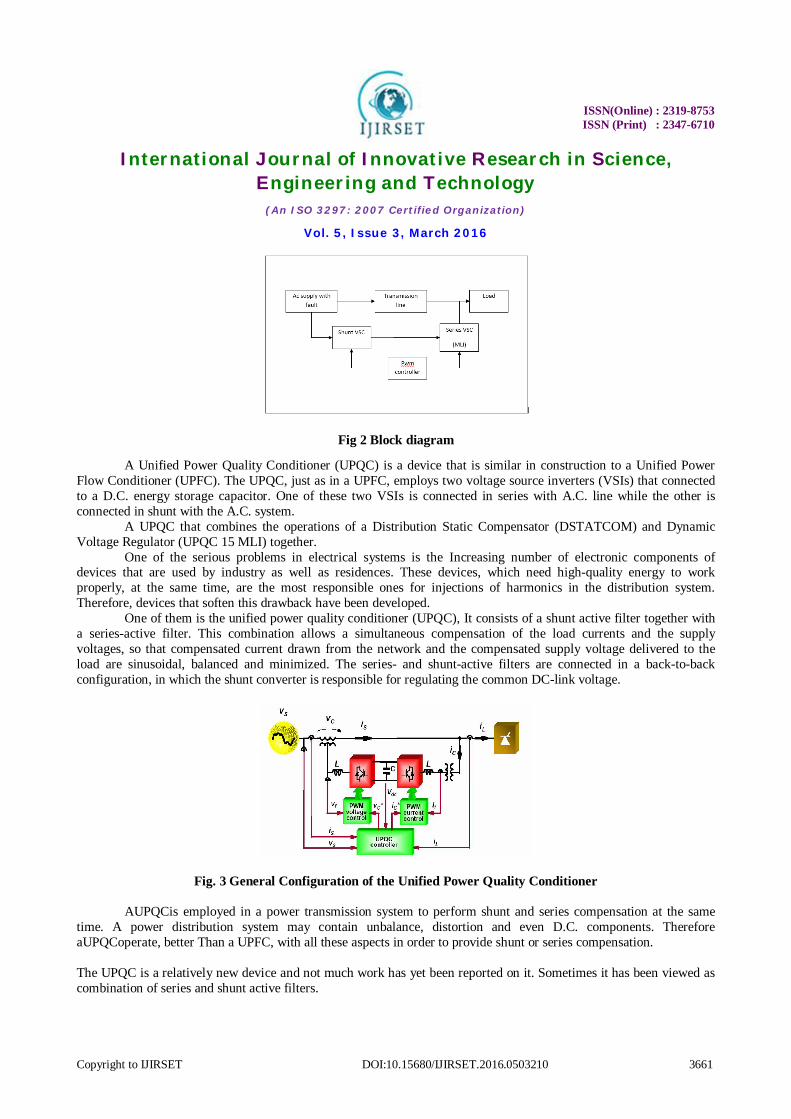
One of the serious problems in electrical systems is the Increasing number of electronic components of devices that are used by industry as well as residences. These devices, which need high-quality energy to work properly, at the same time, are the most responsible ones for injections of harmonics in the distribution system. Therefore, devices that soften this drawback have been developed.
One of them is the unified power quality conditioner (UPQC), It consists of a shunt active filter together with a series-active filter. This combination allows a simultaneous compensation of the load currents and the supply voltages, so that compensated current drawn from the network and the compensated supply voltage delivered to the load are sinusoidal, balanced and minimized. The series- and shunt-active filters are connected in a back-to-back configuration, in which the shunt converter is responsible for regulating the common DC-link voltage.
Fig. 3 General Configuration of the Unified Power Quality Conditioner
AUPQCis employed in a power transmission system to perform shunt and series compensation at the same time. A power distribution system may contain unbalance, distortion and even D.C. components. Therefore aUPQCoperate, better Than a UPFC, with all these aspects in order to provide shunt or series compensation.
The UPQC is a relatively new device and not much work has yet been reported on it. Sometimes it has been viewed as combination of series and shunt active filters.
ISSN(Online) : 2319-8753 ISSN (Print) : 2347-6710
International Journal of Innovative Research in Science, Engineering and Technology
(An ISO 3297: 2007 Certified Organization)
Vol. 5, Issue 3, March 2016
Copyright to IJIRSET DOI:10.15680/IJIRSET.2016.0503210 3662
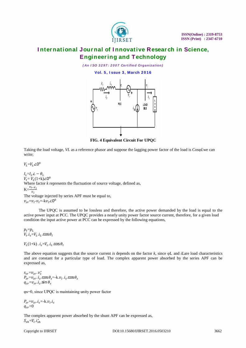
FIG. 4 Equivalent Circuit For UPQC
Taking the load voltage, VL as a reference phasor and suppose the lagging power factor of the load is CosφLwe can write; 푉 =푉 ∠0 퐼 =퐼 ∠ − 휃 푉 = 푉 (1+k)∠0 Where factor k represents the fluctuation of source voltage, defined as, K= The voltage injected by series APF must be equal to, 푣 =푣 -푣 =-k푣 ∠0
The UPQC is assumed to be lossless and therefore, the active power demanded by the load is equal to the active power input at PCC. The UPQC provides a nearly unity power factor source current, therefore, for a given load condition the input active power at PCC can be expressed by the following equations, 푝 =푝 푉 .푖 =푉 .푖 .cos휃 푉 (1+k). 푖 =푉 .푖 .cos휃 The above equation suggests that the source current is depends on the factor k, since φL and iLare load characteristics and are constant for a particular type of load. The complex apparent power absorbed by the series APF can be expressed as, 푠 =푣 .푣∗ 푃 =푣 . 푖 .cos휃 =-k.푣 . 푖 .cos휃 푞 =푣 .푖 .sin휃 φs=0, since UPQC is maintaining unity power factor 푃 =푣 .푖 =-k.푣 .푖 푞 =0 The complex apparent power absorbed by the shunt APF can be expressed as, 푆 =푉 .푖∗
ISSN(Online) : 2319-8753 ISSN (Print) : 2347-6710
International Journal of Innovative Research in Science, Engineering and Technology
(An ISO 3297: 2007 Certified Organization)
Vol. 5, Issue 3, March 2016
Copyright to IJIRSET DOI:10.15680/IJIRSET.2016.0503210 3663
The current provided by the shunt APF, is the difference between the Input source current and the load current, which includes the load Harmonics current and the reactive current. Therefore, we can write; 푖 =푖 -푖 푖 =푖 ∠0 -푖 ∠-휃 푖 =푖 -(푖 .cos휃 -푗푖 .sin휃 )=(푖 -푖 . cos휃 )+푗푖 . sin휃 푝 =푉 .푖 .cos휃 =푉 .푖 .sin휃 푞 =푉 .푖 . sin휃 =푉 .푖 .sin휃 Based on the above analysis the different modes of operation are discussed
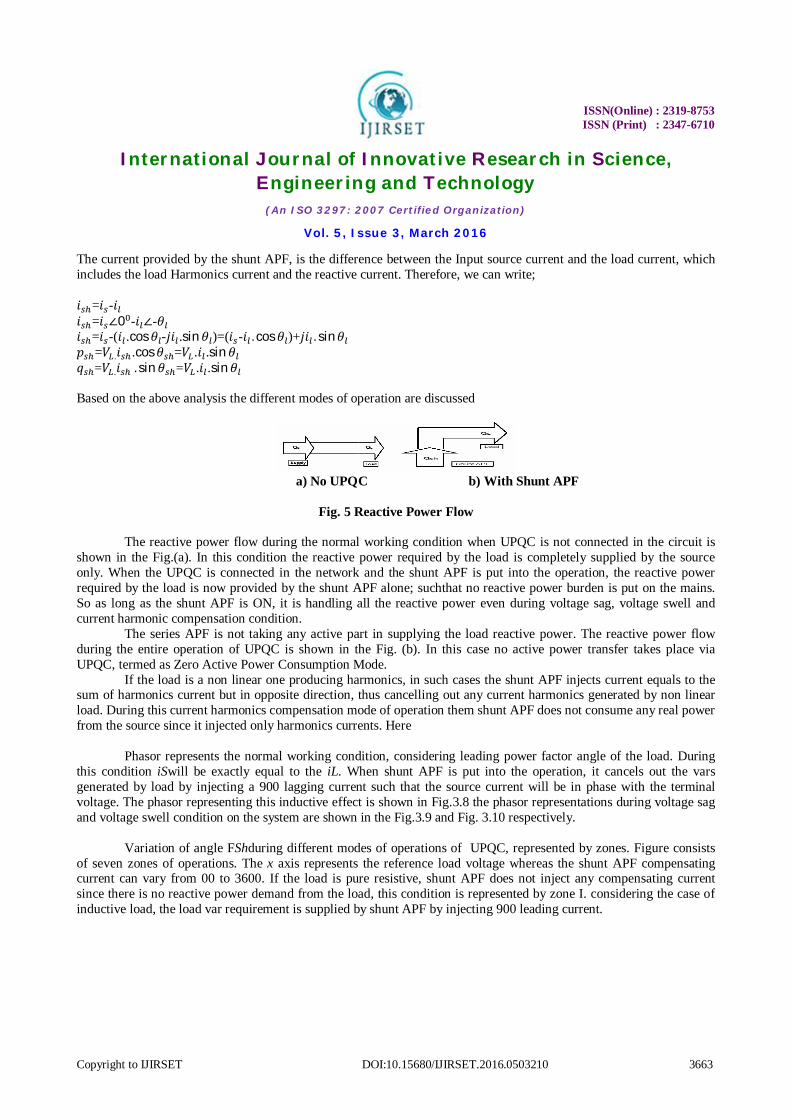
a) No UPQC b) With Shunt APF
Fig. 5 Reactive Power Flow
The reactive power flow during the normal working condition when UPQC is not connected in the circuit is
shown in the Fig.(a). In this condition the reactive power required by the load is completely supplied by the source only. When the UPQC is connected in the network and the shunt APF is put into the operation, the reactive power required by the load is now provided by the shunt APF alone; suchthat no reactive power burden is put on the mains. So as long as the shunt APF is ON, it is handling all the reactive power even during voltage sag, voltage swell and current harmonic compensation condition.
The series APF is not taking any active part in supplying the load reactive power. The reactive power flow during the entire operation of UPQC is shown in the Fig. (b). In this case no active power transfer takes place via UPQC, termed as Zero Active Power Consumption Mode.
If the load is a non linear one producing harmonics, in such cases the shunt APF injects current equals to the sum of harmonics current but in opposite direction, thus cancelling out any current harmonics generated by non linear load. During this current harmonics compensation mode of operation them shunt APF does not consume any real power from the source since it injected only harmonics currents. Here
Phasor represents the normal working condition, considering leading power factor angle of the load. During this condition iSwill be exactly equal to the iL. When shunt APF is put into the operation, it cancels out the vars generated by load by injecting a 900 lagging current such that the source current will be in phase with the terminal voltage. The phasor representing this inductive effect is shown in Fig.3.8 the phasor representations during voltage sag and voltage swell condition on the system are shown in the Fig.3.9 and Fig. 3.10 respectively.
Variation of angle FShduring different modes of operations of UPQC, represented by zones. Figure consists of seven zones of operations. The x axis represents the reference load voltage whereas the shunt APF compensating current can vary from 00 to 3600. If the load is pure resistive, shunt APF does not inject any compensating current since there is no reactive power demand from the load, this condition is represented by zone I. considering the case of inductive load, the load var requirement is supplied by shunt APF by injecting 900 leading current.
ISSN(Online) : 2319-8753 ISSN (Print) : 2347-6710
International Journal of Innovative Research in Science, Engineering and Technology
(An ISO 3297: 2007 Certified Organization)
Vol. 5, Issue 3, March 2016
Copyright to IJIRSET DOI:10.15680/IJIRSET.2016.0503210 3664
IV. CIRCUIT TOPOLOGY
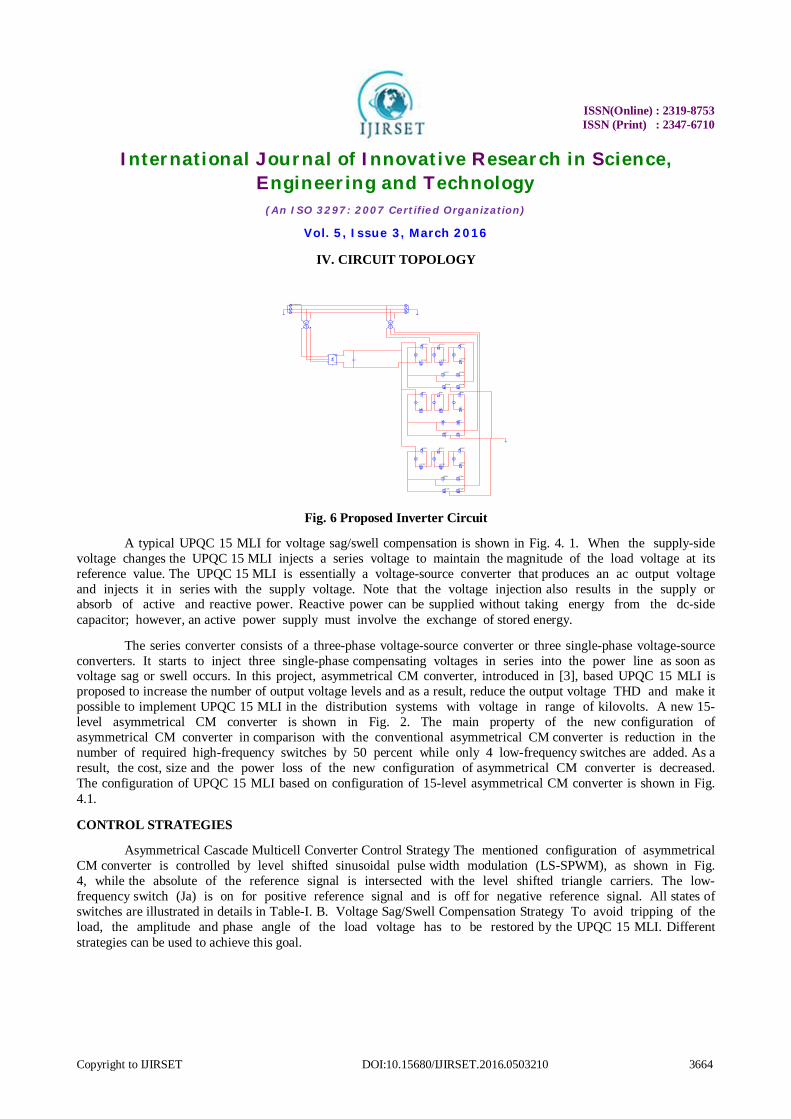
Fig. 6 Proposed Inverter Circuit
A typical UPQC 15 MLI for voltage sag/swell compensation is shown in Fig. 4. 1. When the supply-side voltage changes the UPQC 15 MLI injects a series voltage to maintain the magnitude of the load voltage at its reference value. The UPQC 15 MLI is essentially a voltage-source converter that produces an ac output voltage and injects it in series with the supply voltage. Note that the voltage injection also results in the supply or absorb of active and reactive power. Reactive power can be supplied without taking energy from the dc-side capacitor; however, an active power supply must involve the exchange of stored energy.
The series converter consists of a three-phase voltage-source converter or three single-phase voltage-source converters. It starts to inject three single-phase compensating voltages in series into the power line as soon as voltage sag or swell occurs. In this project, asymmetrical CM converter, introduced in [3], based UPQC 15 MLI is proposed to increase the number of output voltage levels and as a result, reduce the output voltage THD and make it possible to implement UPQC 15 MLI in the distribution systems with voltage in range of kilovolts. A new 15-level asymmetrical CM converter is shown in Fig. 2. The main property of the new configuration of asymmetrical CM converter in comparison with the conventional asymmetrical CM converter is reduction in the number of required high-frequency switches by 50 percent while only 4 low-frequency switches are added. As a result, the cost, size and the power loss of the new configuration of asymmetrical CM converter is decreased. The configuration of UPQC 15 MLI based on configuration of 15-level asymmetrical CM converter is shown in Fig. 4.1.
CONTROL STRATEGIES
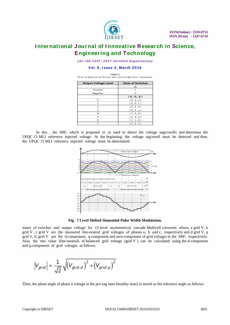
Asymmetrical Cascade Multicell Converter Control Strategy The mentioned configuration of asymmetrical CM converter is controlled by level shifted sinusoidal pulse width modulation (LS-SPWM), as shown in Fig. 4, while the absolute of the reference signal is intersected with the level shifted triangle carriers. The low-frequency switch (Ja) is on for positive reference signal and is off for negative reference signal. All states of switches are illustrated in details in Table-I. B. Voltage Sag/Swell Compensation Strategy To avoid tripping of the load, the amplitude and phase angle of the load voltage has to be restored by the UPQC 15 MLI. Different strategies can be used to achieve this goal.
threephasesupply
V SC
C
s1bar S2bar S3bar
Jbar J
S3S2S1
J Jbar
MOS35 MOS36 MOS37
MOS38 MOS39
MOS40MOS41MOS42
MOS43 MOS44
MOS45 MOS46 MOS47
MOS48 MOS49
MOS50MOS51MOS52
MOS53 MOS54
ISSN(Online) : 2319-8753 ISSN (Print) : 2347-6710
International Journal of Innovative Research in Science, Engineering and Technology
(An ISO 3297: 2007 Certified Organization)
Vol. 5, Issue 3, March 2016
Copyright to IJIRSET DOI:10.15680/IJIRSET.2016.0503210 3665
In this , the SRF, which is proposed in ,is used to detect the voltage sags/swells and determine the UPQC 15 MLI reference injected voltage. At the beginning, the voltage sag/swell must be detected and then, the UPQC 15 MLI reference injected voltage must be determined.
Fig. 7 Level Shifted Sinusoidal Pulse Width Modulation.
states of switches and output voltage for 15-level asymmetrical cascade Multicell converter. where, a grid V, b grid V , c grid V are the measured line-neutral grid voltages of phases a, b and c, respectively and d grid V, q grid V, 0, grid V are the d-component, q-component and zero-component of grid voltages in the SRF, respectively. Also, the rms value (line-neutral) of balanced grid voltage (grid V ) can be calculated using the d-component and q-component of grid voltages as follows:
Then, the phase angle of phase a voltage in the pre-sag state (healthy state) is stored as the reference angle as follows:
ISSN(Online) : 2319-8753 ISSN (Print) : 2347-6710
International Journal of Innovative Research in Science, Engineering and Technology
(An ISO 3297: 2007 Certified Organization)
Vol. 5, Issue 3, March 2016
Copyright to IJIRSET DOI:10.15680/IJIRSET.2016.0503210 3666
Components of grid voltages in the SRF, respectively. In the case of single phase voltage sag/swell or unbalanced three phase voltage sag/swell, the zero-component of grid voltages in the SRF is not nil. Therefore, it can be used as a parameter to detect the voltage sag/swell.
However, in the case of balanced three phase voltage sag/swell, the zero-component of grid voltages in the SRF is nil and only the rms value of balanced grid voltage in the sag/swell state changes. Because of that, it is necessary to use the rms value of line-neutral grid voltages (grid V ) obtained from (2) as another parameter to detect the voltage sag/swell. Finally, the following proposed algorithm based on two steps is performed iteratively to detect the voltage sag/swell: Step-1: The zero-component of grid voltages in the SRF which is obtained from (1) is analyzed.
If it is not equal zero, it means that the unbalanced voltage sag/swell is occurred. So, the voltage sag/swell is detected and then, exit the algorithm. If the zero component is equal to zero, go to step-2. The nil zero-component means that the grid voltages are balanced. So, the rms value of grid voltages must be analyzed as step-2. Step-2: The rms value of line-neutral grid voltages (grid V ) obtained from (2) is compared with the reference rms value of line-neutral grid voltages ( ref rms V ). If they are not equal to each other, it means that the voltage sag/swell is occurred. So, the voltage sag/swell is detected and then, exit the algorithm.
If there is no difference between them, go to step-1. Using the balanced or unbalanced voltage sag/swell. After the detection of voltage sag/swell, the reference rms value of line-neutral grid voltages (ref rms V ) and the obtained reference angle (ref θ ) are used to determine the values of reference grid voltages in the SRF as follows: explained algorithm makes it possible to detect any
ISSN(Online) : 2319-8753 ISSN (Print) : 2347-6710
International Journal of Innovative Research in Science, Engineering and Technology
(An ISO 3297: 2007 Certified Organization)
Vol. 5, Issue 3, March 2016
Copyright to IJIRSET DOI:10.15680/IJIRSET.2016.0503210 3667
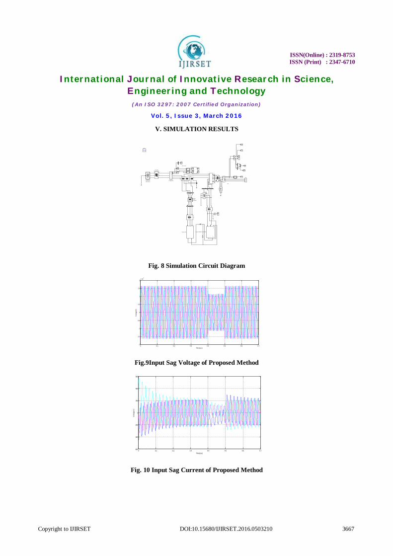
V. SIMULATION RESULTS
Fig. 8 Simulation Circuit Diagram
Fig.9Input Sag Voltage of Proposed Method
Fig. 10 Input Sag Current of Proposed Method
IN PUT VO LTAGE
G RID
A B C
+ -
three phase inverter
-K-
rmsi
-K-
rms
D iscret e,Ts = 5e- 005 s.
powergui
Con n1Con n2
Con n3
load
A1
B1
C1
A2
B2
C2
A
B
C
in jected trans former 1
v+-
Va bcIa bc
A
B
C
abc
Vab c
Iab cA
B
C
a
b
cTh ree-Phase
V -I Measuremen t
A B C
a b c
Three-P haseTransformer(Two Windings)2
A
B
C
A
B
C
Th ree-PhaseSer ies R LC B ra nch1
N
A
B
C
Three-P haseProgra mma bleVoltag e S ource
SOU RCE V4
Vab c
Iab c
Ma g _V_I
P_QPQ &VI5
Va bcIa bc
Ma g_ V_IP_ Q
Va bcIa bc
Ma g_ V_IP_ Q
12
12Lin ear Tran sform er2
12Lin ear Tra nsformer1
A B C
A B C
L f4
A B C
A B C
L f3
A
B
C
A
B
C
Lf1
A B C
A B C
L f
A
B
C
A
B
C
Cf
Va
bc
Iabc
A B C
a b c
A
B
C
a
b
c
B4
A B C
a b c B 3
A B C
a b c B1
A C
DC
-
B DC
+
15 LEVE L A SYMME RICAL CM CONV ERTER
0 0.1 0.2 0.3 0.4 0.5 0.6 0.7-2
-1.5
-1
-0.5
0
0.5
1
1.5
2x 10
4
Time(sec)
Vol
tage
(V)
0 0.1 0.2 0.3 0.4 0.5 0.6 0.7-600
-400
-200
0
200
400
600
Time(sec)
Vol
tage
V)
ISSN(Online) : 2319-8753 ISSN (Print) : 2347-6710
International Journal of Innovative Research in Science, Engineering and Technology
(An ISO 3297: 2007 Certified Organization)
Vol. 5, Issue 3, March 2016
Copyright to IJIRSET DOI:10.15680/IJIRSET.2016.0503210 3668
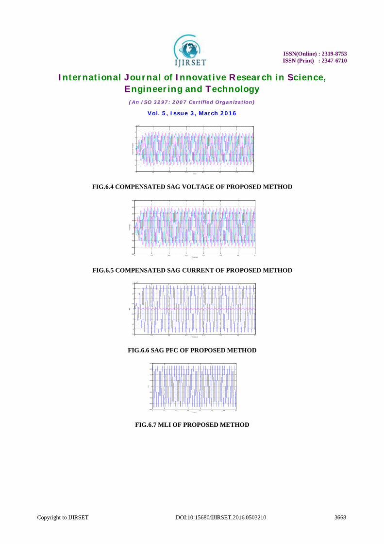
FIG.6.4 COMPENSATED SAG VOLTAGE OF PROPOSED METHOD
FIG.6.5 COMPENSATED SAG CURRENT OF PROPOSED METHOD
FIG.6.6 SAG PFC OF PROPOSED METHOD
FIG.6.7 MLI OF PROPOSED METHOD
0 0.1 0.2 0.3 0.4 0.5 0.6 0.7-4
-3
-2
-1
0
1
2
3
4x 10
4
Time
com
pens
ate
Vol
tage
(V)
0 0.1 0.2 0.3 0.4 0.5 0.6 0.7-800
-600
-400
-200
0
200
400
600
800
Time(sec)
Cur
rent
(I)
0 0.1 0.2 0.3 0.4 0.5 0.6 0.7-2.5
-2
-1.5
-1
-0.5
0
0.5
1
1.5
2
2.5x 10
4
Time(sec)
PFC
0 0.1 0.2 0.3 0.4 0.5 0.6 0. 7-8000
-6000
-4000
-2000
0
2000
4000
6000
8000
Time(sec)
MLI
ISSN(Online) : 2319-8753 ISSN (Print) : 2347-6710
International Journal of Innovative Research in Science, Engineering and Technology
(An ISO 3297: 2007 Certified Organization)
Vol. 5, Issue 3, March 2016
Copyright to IJIRSET DOI:10.15680/IJIRSET.2016.0503210 3669
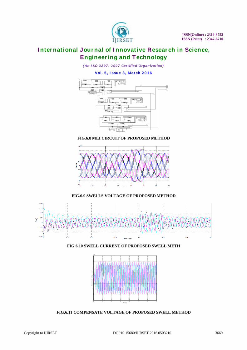
FIG.6.8 MLI CIRCUIT OF PROPOSED METHOD
FIG.6.9 SWELLS VOLTAGE OF PROPOSED METHOD
FIG.6.10 SWELL CURRENT OF PROPOSED SWELL METH
FIG.6.11 COMPENSATE VOLTAGE OF PROPOSED SWELL METHOD
ja
ja
ja1
ja1
S1
S 11
S2 S3
S31S 21
ja
ja
ja1
ja1
S1
S11
S2 S 3
S31S21
ja
ja
ja1
ja1
S 1
S11
S 2 S3
S31S21
5DC -
4DC +
3C
2B
1A
v
+
-
v
+
-
v
+
-
sine wav es 3
s33
Su bsystem8
sin e wav es2
s22
Su bsystem7
sin e wav es1
s11
Su bsystem6
sine wav es1
s11
Sub syste m5
sine wav es2
s22
Sub syste m4
sine wav es3
s33
Sub syste m3
sine waves1
s11
Subsyste m2
sine waves2
s22
Sub syste m1
sine waves3
s33
Sub sy ste m
Sin e Wa ve4
Sine Wave 1
Sine Wave
>=
Rel ati on alO pe rat or7
>=
Rela tio na lOp er ato r2
>=
Re lat ion alOpe ra tor 1
NOT
NOT
NOT
g m
C E
g m
C E
g m
C E
gm
CE
g m
C E
gm
CE
g m
C E
gm
CE
g m
C E
g m
C E
gm
CE
g m
C E
gm
CE
gm
CE
g m
C E
g m
C E
g m
C E
g m
C E
g m
C E
g m
C E
g m
C E
gm
CE
g m
C E
gm
CE
gm
CE
g m
C E
g m
C E
g m
C E
g m
C E
g m
C E
0
Co nsta nt2
0
Con stan t1
0
Con stan t
0 0.1 0.2 0.3 0.4 0.5 0.6 0.7-4
-3
-2
-1
0
1
2
3
4x 10
4
Time(sec)
Com
pens
ated
vol
tage
in s
wel
l
ISSN(Online) : 2319-8753 ISSN (Print) : 2347-6710
International Journal of Innovative Research in Science, Engineering and Technology
(An ISO 3297: 2007 Certified Organization)
Vol. 5, Issue 3, March 2016
Copyright to IJIRSET DOI:10.15680/IJIRSET.2016.0503210 3670
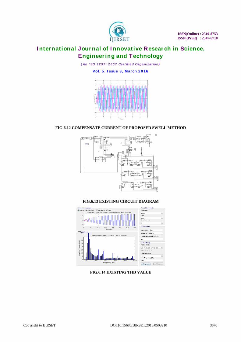
FIG.6.12 COMPENSATE CURRENT OF PROPOSED SWELL METHOD
FIG.6.13 EXISTING CIRCUIT DIAGRAM
FIG.6.14 EXISTING THD VALUE
0 0.1 0.2 0.3 0.4 0.5 0.6 0.7-800
-600
-400
-200
0
200
400
600
800
Time(sec)
Com
pens
ate(
Curre
nt)
kS2
s1J
kS2
kS2
sag
Di scre te ,Ts = 2e-005 s.
powergui
A
B
C
+
-
non linear load
A1
B1
C1
A2
B2
C2
A
B
C
in ject ed tra nsfor me r
N
A
B
C
V oltage Source
v+-
V1V
g
A
B
C
+
-
A
B
C
A
B
C
A B C
a b c
VabcIabc
A
B
C
abc
VabcI abc
A
B
C
abc
VabcI abc
A
B
C
abc
A B C
a b c
A
B
C
A
B
C
Out1
Sub syste m6
Out1
Sub syste m5
Out1
Sub syste m4
Out1
Sub syste m3
Out1
Sub system 2
Out1
Sub syste m1
VA
VA 1
VA 2
SE RIES PULS E
sag detec
sag detec pulse
Sub syste m
Sco pe 6
Scop e3
Sco pe 2
Scop e1
Scop e
SO URCE V SOURCE I
RL 3
RL 2
12
12
12
A
B
C
A
B
C
L f3
A
B
C
A
B
C
L f2
A B C
A B C
Lf
INJECTED VO LTAGE AND CURRENT
g
CE
g
CE
g
CE
g
CE
g
CE g
CE
g
CE
g
CE
g
CE
g
CE
g
CE
g
CE
g
CE g
CE
g
CEg
CE
g
CE
g
CE
g
CE g
CE
g
CEg
CE
g
CE
g
CE
I 2I
DC Voltage
A
B
C
A
B
C
Cf
B reaker2Breaker1B reaker
Vabc
Iabc
A B Ca b c B3
Vabc
Iabc
A B Ca b cB2
Vabc
Iabc
A B Ca b c B1
NOT9
NO T8 NOT7
NOT
6
NO T5 NOT4
abc
Mag
Phase
abcMag
Phase
NOT3
NOT2 NOT1
v+- 2
v+-
1
NO T 2
NO T 1
NO T
v+-
0 0.1 0.2 0.3 0.4 0.5 0.6 0.7
-5
0
5
Selected signal: 35 cycles. FFT window (in red): 3 cycles
Time (s)
0 200 400 600 800 10000
5
10
15
20
25
30
Frequency (Hz)
Fundamental (50Hz) = 0.9434 , THD= 29.82%
Mag
(% o
f Fun
dam
enta
l)
ISSN(Online) : 2319-8753 ISSN (Print) : 2347-6710
International Journal of Innovative Research in Science, Engineering and Technology
(An ISO 3297: 2007 Certified Organization)
Vol. 5, Issue 3, March 2016
Copyright to IJIRSET DOI:10.15680/IJIRSET.2016.0503210 3671
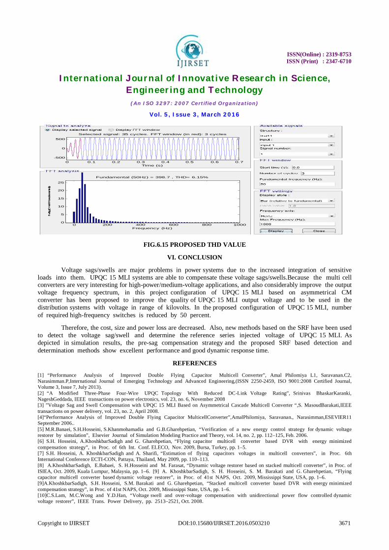
FIG.6.15 PROPOSED THD VALUE
VI. CONCLUSION
Voltage sags/swells are major problems in power systems due to the increased integration of sensitive loads into them. UPQC 15 MLI systems are able to compensate these voltage sags/swells.Because the multi cell converters are very interesting for high-power/medium-voltage applications, and also considerably improve the output voltage frequency spectrum, in this project configuration of UPQC 15 MLI based on asymmetrical CM converter has been proposed to improve the quality of UPQC 15 MLI output voltage and to be used in the distribution systems with voltage in range of kilovolts. In the proposed configuration of UPQC 15 MLI, number of required high-frequency switches is reduced by 50 percent.
Therefore, the cost, size and power loss are decreased. Also, new methods based on the SRF have been used to detect the voltage sag/swell and determine the reference series injected voltage of UPQC 15 MLI. As depicted in simulation results, the pre-sag compensation strategy and the proposed SRF based detection and determination methods show excellent performance and good dynamic response time.
REFERENCES
[1] “Performance Analysis of Improved Double Flying Capacitor Multicell Converter”, Amal Philomiya L1, Saravanan.C2, Narasimman.P,International Journal of Emerging Technology and Advanced Engineering,(ISSN 2250-2459, ISO 9001:2008 Certified Journal, Volume 3, Issue 7, July 2013). [2] “A Modified Three-Phase Four-Wire UPQC Topology With Reduced DC-Link Voltage Rating”, Srinivas BhaskarKaranki, NageshGeddada, IEEE transactions on power electronics, vol. 23, no. 6, November 2008 [3] ”Voltage Sag and Swell Compensation with UPQC 15 MLI Based on Asymmetrical Cascade Multicell Converter “,S. MasoudBarakati,IEEE transactions on power delivery, vol. 23, no. 2, April 2008. [4]“Performance Analysis of Improved Double Flying Capacitor MulticellConverter”,AmalPhilomiya, Saravanan., Narasimman,ESEVIER11 September 2006.. [5] M.R.Banaei, S.H.Hosseini, S.Khanmohamadia and G.B.Gharehpetian, “Verification of a new energy control strategy for dynamic voltage restorer by simulation”, Elsevier Journal of Simulation Modeling Practice and Theory, vol. 14, no. 2, pp. 112–125, Feb. 2006. [6] S.H. Hosseini, A.KhoshkbarSadigh and G. Gharehpetian, “Flying capacitor multicell converter based DVR with energy minimized compensation strategy”, in Proc. of 6th Int. Conf. ELECO, Nov. 2009, Bursa, Turkey, pp. 1–5. [7] S.H. Hosseini, A. KhoshkbarSadigh and A. Sharifi, “Estimation of flying capacitors voltages in multicell converters”, in Proc. 6th International Conference ECTI-CON, Pattaya, Thailand, May 2009, pp. 110–113. [8] A.KhoshkbarSadigh, E.Babaei, S. H.Hosseini and M. Farasat, “Dynamic voltage restorer based on stacked multicell converter”, in Proc. of ISIEA, Oct. 2009, Kuala Lumpur, Malaysia, pp. 1–6. [9] A. KhoshkbarSadigh, S. H. Hosseini, S. M. Barakati and G. Gharehpetian, “Flying capacitor multicell converter based dynamic voltage restorer”, in Proc. of 41st NAPS, Oct. 2009, Mississippi State, USA, pp. 1–6. [9]A.KhoshkbarSadigh, S.H. Hosseini, S.M. Barakati and G. Gharehpetian, “Stacked multicell converter based DVR with energy minimized compensation strategy”, in Proc. of 41st NAPS, Oct. 2009, Mississippi State, USA, pp. 1–6. [10]C.S.Lam, M.C.Wong and Y.D.Han, “Voltage swell and over-voltage compensation with unidirectional power flow controlled dynamic voltage restorer”, IEEE Trans. Power Delivery, pp. 2513–2521, Oct. 2008.
0 0.1 0.2 0.3 0.4 0.5 0.6 0.7-500
0
500
Selected signal: 35 cycles. FFT window (in red): 3 cycles
Time (s)
0 200 400 600 800 10000
5
10
15
20
25
Frequency (Hz)
Fundamental (50Hz) = 398.7 , THD= 6.15%
Mag (%
of F
undamental)
ISSN(Online) : 2319-8753 ISSN (Print) : 2347-6710
International Journal of Innovative Research in Science, Engineering and Technology
(An ISO 3297: 2007 Certified Organization)
Vol. 5, Issue 3, March 2016
Copyright to IJIRSET DOI:10.15680/IJIRSET.2016.0503210 3672
[11]J. Lamoree, L. Tang, C. DeWinkel, and P. Vinett, “Description of a micro-SMES system for protection of critical customer facilities”, IEEE Trans. Power Delivery, vol. 9, no. 2, pp. 984–991, Apr. 1994. [12]S.A. Saleh, C. R. Moloney and M. A. Rahman, “Implementation of a dynamic voltage restorer system based on discrete wavelet transforms”, IEEE Trans. Power Delivery, vol. 23, no. 4, pp. 2366–2375, Oct. 2008. [13]P.R.Sánchez, E.Acha, J. E. O. Calderon, V. Feliu and A. G. Cerrada, “A Versatile control scheme for a dynamic voltage restorer for power-quality improvement”, IEEE Trans. Power Delivery, vol. 24, no. 1, pp. 277–284, Jan. 2009. [14]B.Wang and G.Venkataramanan, “Dynamic voltage restorer utilizing a matrix converter and flywheel energy storage”, IEEE Trans. Industry Applications, vol. 45, no. 1, pp. 222–231, Jan./Feb. 2009. [15]M.A.Pérez, P.Cortés and José Rodríguez, “Predictive control algorithm technique for multilevel asymmetric cascaded H-bridge inverters”, IEEE Trans. Industrial Electronics, vol. 55, no. 12, pp. 4354-4361, Dec. 2008.