vlc modulation schemes - universidade de aveiro d4.1 - vlc modulati… · the vidas project....
TRANSCRIPT
VIDAS PTDC/EEA-TEL/75217/2006
Deliverable D4.1
VLC Modulation Schemes
Instituto de Telecomunicações
Pólo de Aveiro
Aveiro, July 31st, 2010


Deliverable D 4.1:
Modulation Schemes
Authors: Navin Kumar
Mónica Figueiredo
Luis Nero Alves
Rui L. Aguiar
Source: Instituto de Telecomunicações - Pólo de Aveiro
No. of pages: 94
Version: 1
Date: March 31st, 2011
This deliverable reports to:
Activity D4.1: Modulation Schemes for outdoor visible-light communication systems


Modulation Schemes VIDAS Project
Instituto de Telecomunicações – Pólo de Aveiro i
Contents
Summary ................................................................................................................................... 1
1.Introduction ........................................................................................................................... 2
2.Baseband Data Transmission in White Gaussian Noise and Probability of Error ........ 4
3.Basic Modulation Techniques .............................................................................................. 7
3.1 On-off Keying – Non Return to Zero (NRZ) ........................................................................... 7
3.1.1 BER for OOK Modulation .................................................................................................................. 9
3.2 Pulse Position Modulation (PPM) .......................................................................................... 10
3.2.1 Bit Error Rate of L-PPM .................................................................................................................. 11 3.2.2 Inverted – PPM (I-PPM) .................................................................................................................. 12
3.2.2.1 Bit Error Rate of I-LPPM ............................................................................................................................. 13
4.Direct Sequence Spread Spectrum .................................................................................... 15
4.1 Introduction ............................................................................................................................ 15 4.2 DSSS Modulation in VLC System ......................................................................................... 18
4.2.1 Introduction ...................................................................................................................................... 18 4.2.2 Basic Principle ................................................................................................................................. 18 4.2.3 Sequence Inverse Keying Modulator ................................................................................................ 19
4.2.3.1 Frequency Domain Analysis ........................................................................................................................ 19
4.2.3.2 The Corresponding Time Domain Analysis ................................................................................................. 22
4.3 SNR and BER of SIK Modulator with AWGN ...................................................................... 23 4.4 SNR and BER of SIK Modulator in the Presence of External Noise ..................................... 23 4.5 Matlab Simulink Model For DSSS SIK ................................................................................. 24
4.5.1 Integrate and Dump Decorrelator Receiver ..................................................................................... 25 4.5.2 PN Matched Filter Correlator Receiver........................................................................................... 27
4.5.2.1 PN Code Generator ...................................................................................................................................... 28
5.Uncertainty in Clock Repeaters ......................................................................................... 31
5.1 Clock Repeaters .................................................................................................................... 31 5.2 Simulation Framework ........................................................................................................ 36 5.3 Performance Analysis ........................................................................................................... 41
6.Uncertainty in Cascaded Clock Repeaters ........................................................................ 45
6.1 Digitally Controlled Delay Lines ......................................................................................... 45 6.2 Performance Analysis ............................................................................................................. 47 6.3 Clock Distribution Trees ........................................................................................................ 50
7.Jitter Accumulation Model ................................................................................................. 54

Modulation Schemes VIDAS Project
Instituto de Telecomunicações – Pólo de Aveiro ii
7.1 Dynamic Jitter in Cascaded Repeaters ................................................................................... 54 7.2 Bounds for Jitter Accumulation ............................................................................................ 56 7.3 Simulation Results ............................................................................................................... 58
8.Performance Results ........................................................................................................... 62
9.Concluding Remarks........................................................................................................... 68
References ............................................................................................................................... 69

Modulation Schemes VIDAS Project
Instituto de Telecomunicações – Pólo de Aveiro 1 / 94
Modulation Schemes
Project VIDAS: Deliverable D4.1
PTDC/EEA-TEL/75217/2006
Summary
This report presents the analysis of different modulation schemes D4.1 for VLC systems of
the VIDAS project.
Considering the final prototype design and application, the deliverable D4.1 was projected.
The detail analysis of various modulation schemes are carried out and a robust technique
based on direct sequence spread spectrum (DSSS) is followed. DSSS technique though
necessitates use of high bandwidth while minimizing the effect of noise. Since the final
application does not require very high data rate of transmission but robustness against the
noise (external lights) becomes necessary. The analysis is followed by model development
using Matlab/Simulink. The performance of both of these systems are compared and
evaluated. Some of the simulation results are presented.

Modulation Schemes VIDAS Project
Instituto de Telecomunicações – Pólo de Aveiro 2 / 94
Section 1
1. Introduction
Modulation is one of the key processes in communication system. Appropriate and robust
modulation techniques allow enhanced performance of the system. The performance of VLC
systems is likely to be impaired by the significant high path loss and the shot noise induced by
natural and artificial lights. High path loss leads to the use of considerably high optical power
levels. In addition, they are also suffered from the speed of optoelectronic devices (LEDs and
PIN photodiodes). System performance varies depending on the environment conditions, data
rate, technical solutions and implementation of a particular system.
In the application of traffic information broadcast system, the data is received by the
receiver installed on moving vehicles. The amount of data received will depend on the data
transmission rate, velocity of vehicles and the road length (service area) in which data is
receivable. This is given by the relation:
(1)
That is, the received data increases with the distance (increase in service area). However, the
possibility of interference also increases with distance. Assuming, a vehicle approaching traffic
point at a speed of 60kmph will cover 16.6m of distance each second. Considering data rate
100kbps, vehicle speed of 60kmph and a service area between 2.5m to 70m of road length, the
amount of received data comes to be approximately 150kbits to 420kbits. Furthermore, a text
message in A4 size of paper with 20 font size of Times New Roman Font which can comfortably
be read by driver contains approximately 10kbits of data. This means that each second 15 to 42

Modulation Schemes VIDAS Project
Instituto de Telecomunicações – Pólo de Aveiro 3 / 94
times of 10kbits of data can be sent by VLC broadcast transmitter and receiver is expected to
reliably receive the information. If the transmitted information is repeated a number of times, the
driver will have little over 4 seconds to read the message before crossing the service area when
green signal remains on (the worst case condition). However, if vehicle needs to stop for green
signal there will not be problem in receiving and reading the information.
The above scenario is applicable in normal conditions i.e. when line-of-sight (LoS) channel is
free from other disturbances such as fog, rain and dense dust. But under these conditions the
channel behavior will vary and thus service area will be affected (as discussed in R3.1).
Therefore, a robust modulation technique is needed for this system. DSSS based modulation has
been widely used in Radio system and considered robust system especially in noisy environment.
However, requirement of transmission bandwidth increases thereby affecting data rate. But, in
road safety applications of traffic information broadcast, the data rate is not an important issue.
Minimizing the effect of external noise is the most important.
In this report, we focus on one of the most robust modulation technique based on DSSS. The
choice for the method is also supported for the low data rate application. The primary measure of
system performance for digital data communication system is the probability of error PE [1].
Therefore, we derive a generic expression for PE and SNR for baseband data transmission on
AWGN channel.

Modulation Schemes VIDAS Project
Instituto de Telecomunicações – Pólo de Aveiro 4 / 94
Section 2
2. Baseband Data Transmission in White Gaussian Noise
and Probability of Error
Consider the binary digital data communication system with transmitted signal consists
of a sequence of constant amplitude pulses of either A or –A units in amplitude and T seconds
duration. Considering a detector with integrate and dump (Fig. 1a), the performance can be
evaluated with probability of error in the received signal. The output of the integrator at the end
of a signaling interval is:
(2)
(3)
where N is a random variable defined as:
(4)
Since N results from a linear operation on a sample function from a Gaussian process, it
is a Gaussian random variable. It has the mean:
(5)

Modulation Schemes VIDAS Project
Instituto de Telecomunicações – Pólo de Aveiro 5 / 94
since n(t) has zero mean. Its variance is therefore,
(6)
where we have made the substitution E{n(t)n(σ)} = ½ [N0 δ(t – σ)]. Using the shifting property
of the delta function, we obtain:
var = ½ (N0T) (7)
Thus the probability density function (pdf) of N is:
(8)
where η is used as the dummy variable for N to avoid confusion with n(t).
If +A is transmitted, an error occurs if AT + N < 0, that is if N < -AT. The probability of
this event is:
(9)
Which is the area to the left of η = -AT in Fig. 1b. Letting:
, we can write this as:
(10)
which is the area to the right of η = AT in the Fig. 1b. The average probability of error is
PE = P(E| +A) P(+A) + P(E| -A) P(-A) . (11)
As P(+A) + P(-A) = 1, we obtain:
(12)
(a) (b)
Fig.1: a) Receiver structure with Integrate-and-dump receiver; b): Illustration of error probabilities for Binary
Signalling

Modulation Schemes VIDAS Project
Instituto de Telecomunicações – Pólo de Aveiro 6 / 94
We can interpret the ratio A2T/N0 in two ways. First, since the energy in each signal pulse is:
(13)
we see that the ratio of signal energy per pulse to noise power spectral density is:
(14)
where Eb is called the energy per bit because each signal pulse (+A or –A) carries one bit of
information. Second, we recall that a rectangular pulse of duration T seconds has amplitude
spectrum AT sinc Tf and that Rb = 1/T is a rough measure of its bandwidth. Thus,
(15)
can be interpreted as a function of bandwidth (data rate).
Next, we examine the performance of various modulation techniques. We start with most
common, based on intensity modulation with direct detection (IM/DD), on-off keying.

Modulation Schemes VIDAS Project
Instituto de Telecomunicações – Pólo de Aveiro 7 / 94
Section 3
3. Basic Modulation Techniques
The choice of modulation technique in the design of VLC system remains one of the
most important technical issues. Background from IR technology suggests the use of modulation
techniques such as OOK, L-pulse position modulation (L-PPM), subcarrier phase shift keying
(SC-PSK) and these have been discussed and proposed [2-4]. Utilization of equalization
techniques for IR as well as indoor short range VLC has also been proposed by authors in [5, 6].
The use of equalizers substantially increases the receiver complexity while OOK and L-PPM
though simple to implement causes interference because of artificial and other sources of light.
In the following sections, we discuss various modulation techniques. We start with OOK,
which forms the basic standard for evaluation.
3.1 On-off Keying – Non Return to Zero (NRZ)
On-Off-Keying is the simplest form of amplitude-shift keying (ASK) modulation that
represents digital data as the presence or absence of a carrier wave. In its simplest form, the
presence of a carrier for a specific duration represents a binary one, while its absence for the
same duration represents a binary zero. Some more sophisticated schemes vary these durations to
convey additional information. It is analogous to unipolar encoding line code.
The block diagram of a typical receiver system employing IM/DD is shown in Fig. 2.
Information bits are the inputs to the modulator (NRZ or Manchester) at a bit rate of Rb (bit per
second (bps)). Pulse waveforms produced by the modulator for each bit drive the optical
Modulation Schemes VIDAS Project
Instituto de Telecomunicações – Pólo de Aveiro 8 / 94
transmitter. The intensity-modulated optical signal passes through a time-dispersive multipath
channel that is fully characterized by its impulse response hc(t). However, multipath channel can
be ignored in this application. The incoming optical signal is converted to an electrical signal by
the photodiode by using direct detection. This electrical signal is comprised of a distorted replica
of the transmitted signal and shot noise, nsh (t), as well as fluorescent light periodic interference,
nfl(t). The high pass filter (HPF) at the receiver front end, after the photodiode, is modeled as a
first-order RC filter with a cut-off frequency of fo. Matched filtering using Integrate and dump
filter is assumed for both modulation schemes. The impulse response of the matched filter for
both modulation schemes is also depicted in Fig. 2. In the absence of fluorescent light and inter
symbol interference (ISI), this corresponds to the optimum maximum-likelihood (ML) receiver
[7].
The peak amplitude of the received signal pulses is A and is directly proportional to the
optical power, i.e., A= 2R Popt, where R is the photodetector responsivity and Popt is the average
received optical power [2, 8]. The power spectral density (PSD) of the Gaussian shot noise nsh (t)
is denoted by N0. The shot noise PSD is dependent on the total DC-generated photocurrent, i.e.,
N0 2e(IB + ib), where IB is the DC photocurrent generated by stationary ambient lighting and ib is
the DC level of the fluorescent light interference. For both modulation schemes the transmitted
signal waveform can be described as an infinite series of time delayed replicas of the basic pulse
waveform p(t):
(16)
where p(t) is the rectangular pulse of duration Tb = 1/Rb. However, if signal is Manchester, the
p(t) is the alternating pulse of the same duration with mid-bit transition.
Fig. 2: Block diagram of a Typical IM/DD Receiver

Modulation Schemes VIDAS Project
Instituto de Telecomunicações – Pólo de Aveiro 9 / 94
Ignoring noise components, the received signal pulse r(t) at the input of the matched filter
will be:
(17)
where hF (t) is the impulse response of the HPF and * denotes convolution.
3.1.1 BER for OOK Modulation
On-Off-Keying transmitter emits a rectangular pulse of duration 1/Rb and of intensity 2P
to signify a one bit, and no pulse to signify a zero bit. The bandwidth required by OOK is
roughly Rb . The BER is given in terms of minimum distance between two bits. In this type of
receiver design, the receiver will choose that signals from the set of known signals that is closest
to the received signal. Since the receiver observes which of the possible signals is closest to the
received signal, it stands to reason that it is less likely to make an error due to noise or other
errors when the other signals are further away.
For the case of OOK the BER is given as:
(18)
Also, in terms of error function1, it is given as:
(19)
Power required by OOK to achieve a given BER is:
(20)
For any other modulation scheme to achieve the same error probability, the required power is
approximately:
(21)
1
and also,

Modulation Schemes VIDAS Project
Instituto de Telecomunicações – Pólo de Aveiro 10 / 94
3.2 Pulse Position Modulation (PPM)
Higher average power efficiency can be achieved by employing pulse modulation
schemes in which a range of time dependent features of a pulse carrier may be used to convey
information.
PPM has been used widely in optical communication systems. It is a scheme where the
pulses of equal amplitude are generated at a rate controlled by the modulating signal's amplitude.
During PPM transmission, signal pulses are fixed width and amplitude, but the actual number is
represented by pulse position in time.
L-PPM utilizes symbols consisting of L time slots (chip). A constant power L.P is
transmitted during these chips and zero during remaining (L-1) chips. Hence, encoding log2L bits
in the position of the high chip. If the amplitude of transmitted waveform is A, average
transmitted power of 2PPM is A/2, that of 4PPM is A/4, and for L-PPM is A/L. For any L greater
than 2, PPM requires less optical power than OOK. In principle, the optical power requirement
can be made arbitrarily small by making L suitably large, at the expense of increased bandwidth.
For a given bit rate, L-PPM requires more bandwidth than OOK by a factor of L/log2L
i.e. 16-PPM requires four times more bandwidth (BW) than OOK. The bandwidth required by
PPM to achieve a bit rate of Rb is approximately the inverse of one chip duration, B = L/T [9]. In
addition to the increased bandwidth requirement, PPM needs (compared to OOK) more
transmitted peak power and both slot and symbol-level synchronization [10].
In the absence of multipath distortion, L-PPM yields an average–power requirement that
decreases steadily with increasing L; the increased noise associated with a (L/log2L)-fold wider
receiver noise BW is out weighted by the L-fold increase in peak power.
Fig. 3 shows the block diagram of the L-PPM system. Input bits, at rate Rb, enter a PPM
encoder, producing L-PPM symbols at rate Rb/Log2L. Each symbol contains a single sample of
unit amplitude and (L-1) samples of zero amplitude. The PPM symbols are converted to a serial
sequence of chips at rate LRb/log2L and passed to a transmitter filter whose impulse response p(t)
is a unit-amplitude rectangular pulse of duration log2L/LRb. The chips are scaled by the peak
detected photocurrent LRP and shot noise n(t) and fluorescent-light interference nfl(t) are added.
The receiver employs a unit- energy filter r(t) matched to p(t) which is followed by high pass
filter h(t). The filtered signal is sampled at rate LRb/log2L and passed to a comparator that
determines which sample in each L-length block has the largest value thus yielding the output bit
sequence. Without fluorescent light and high pass filtering the receiver is ML receiver.

Modulation Schemes VIDAS Project
Instituto de Telecomunicações – Pólo de Aveiro 11 / 94
In this type, each signal is orthogonal of the form:
Xm = [0, 0, ……, bh, 0, 0] (22)
where the non-zero term is in the m-th position. Thus, every signal is the same distance from
every other signal. Fig. 4 illustrates the waveforms from pulse modulators.
3.2.1 Bit Error Rate of L-PPM
For L orthogonal signals, there are (L-1) other signals at the minimum distance, and the
error probability is independent of which signal is transmitted. Symbol error rate can be derived
from minimum Euclidian distance (dmin):
(23)
where dmin for L-PPM is given as:
(24)
Hence, the symbol error rate for L-PPM is given as:
Fig. 3: Block diagram of L-PPM System
Fig.4: Illustration of L-PPM and I-LPPM waveforms
t
A
Tb/4
0 1
00 11
Tb 2Tb0
OOK=>2PPM
4PPM
I-4PPM
t
A
001 010
Tb/8
2TbTb0
10
8PPM
I-8PPM
OOK=>2PPM
Tb/4Tb/8
symbol symbol
Tb/2 3Tb/4 3Tb/8
4Tb/8

Modulation Schemes VIDAS Project
Instituto de Telecomunicações – Pólo de Aveiro 12 / 94
(25)
(26)
BER - We assume that symbol ‘1’ (corresponding to chip sequence bk of a single one
followed by (L-1) zeros) was transmitted and we assume k = L. Therefore, probability of bit error
can be approximated as:
(27)
So that,
(28)
The average optical signal power required to achieve a given SER for an L-PPM system
can be found by solving for Pav:
(29)
(30)
That is, L = 2 yields a sensitivity for 2-PPM that is identical to OOK. We see that, for any L
greater than two, the optical power required by L-PPM is smaller than that required by OOK.
It can also be noted that, 2-PPM has the same power efficiency as OOK but requires
twice the bandwidth. It is apparent that 4-PPM is particularly attractive because it has the same
bandwidth requirement as 2-PPM but requires 3.8dB less optical power. As L increases from 4 to
16, the bandwidth requirement increases from 2Rb to 4Rb, while the sensitivity increases from
3dB better than OOK to 7.5dB better than OOK.
For a given transmitter power, background illumination power, and bit rate, it is desirable
to maximize the allowable distance between transmitter and receiver, which is equivalent to
maximizing the power efficiency.
3.2.2 Inverted – PPM (I-PPM)
In the case of conventional PPM, we set only one pulse among L sub intervals. Average
transmitted power, i.e. LED brightness, falls to 1/L when the peak amplitude is not changed. Of
course, LED brightness can be made to equal with other modulation methods if we increase the

Modulation Schemes VIDAS Project
Instituto de Telecomunicações – Pólo de Aveiro 13 / 94
amplitude L times (practical limitation with power constraint). I-PPM yields higher brightness
than conventional PPM. Inverting the pulse position of conventional PPM, we obtain I-PPM (as
shown in Fig. 4. The optical intensity is ‘off’ during the 1-th sub-interval and ‘on’ everywhere
else. For example, in case of 4-PPM light is on equivalent to 3-chip duration, making the LED
three times as bright as conventional 4PPM. When amplitude of the transmitted waveform is A,
average transmitted power of I-4PPM is 3A/4. That is, the average transmitted power of I-L-PPM
is (L-1)A/L.
This modulation technique is particularly suitable in the indoor environment for the
reason that illumination is better.
3.2.2.1 Bit Error Rate of I-LPPM
In the case of inverted multilevel PPM, the symbol error rate for the inverted L-PPM is
given as:
(31)
(32)
and the BER is therefore;
(33)
The average optical signal power required to achieve a given SER for an I-LPPM system
can be found by solving for Pav:
(34)
(35)
From the simulation results it is observed that L-PPM forms of modulation techniques are
power efficient and can increase the data transmission rate. However, that may result in inter-
symbol interference and increased bandwidth. On the other hand, I-LPPM is suitable for indoor
scenario where power is not a constraint that is required illumination remains to be in place. This
means, they are not power efficient. However, the effect of noise on the systems remains an issue
and in VLC systems the noise effect needs to be minimized. This implies that a different
approach must be considered. From the background on RF technology we know the bandwidth

Modulation Schemes VIDAS Project
Instituto de Telecomunicações – Pólo de Aveiro 14 / 94
spreading can minimize the effect of noise on the channel. In the next section, this issue is
discussed in detail using DSSS technique.

Modulation Schemes VIDAS Project
Instituto de Telecomunicações – Pólo de Aveiro 15 / 94
Section 4
4. Direct Sequence Spread Spectrum
4.1 Introduction
In a direct sequence spread spectrum communication system [11], the spectrum spreading
is accomplished before transmission through the use of a spreading code that is independent of
the data sequence. The same spreading code is used in the receiver (operating in synchronism
with the transmitter) to de-spread the received signal so that the original data may be recovered.
The information-bearing signal is multiplied by a spreading code so that each information bit is
divided into a number of small time increments. These small time increments are commonly
referred to as chips. In this process the narrow bandwidth of the information-bearing signal is
spread over a wide bandwidth with a factor L which equals the length of the spreading sequence.
Spread-spectrum communication techniques may be very useful in solving different
communication problems. The amount of performance improvement that is achieved through the
use of spread-spectrum, relative to an unspread system, is described in terms of a so-called
processing gain (PG) factor. In spread-spectrum modulation an information-bearing signal is
transformed into a transmission signal with a much larger bandwidth. The transformation is
achieved by encoding (spreading) the information bearing signal with a spreading code signal.
This process spreads the power of the original data signal over a much broader bandwidth,
resulting in a lower power spectral density than the unspread information signal. When the
spectral density of the resultant spread spectrum signal starts to merge with or fall below the
background noise level, the DSSS communication signal enters a state of low visibility or

Modulation Schemes VIDAS Project
Instituto de Telecomunicações – Pólo de Aveiro 16 / 94
perception, making it hard to locate or intercept. This communication mode is commonly
referred to as low probability of interception (LPI), and offers a form of security, which has
previously been exploited for military applications, but are presently increasingly applied to a
host of commercial applications. The PG of the spread-spectrum system can be defined as the
ratio of transmission bandwidth to information bandwidth:
(36)
where BT is the transmission bandwidth, BB is the bandwidth of information-bearing signal, Tb is
the one bit period of the data signal, Tc is the one chip period of the spreading code, Rc is the chip
rate of the spreading sequence, Rb is the bit rate of the data signal and L is the length of the
spreading code.
The receiver correlates the received signal with a synchronously generated replica of the
spreading code signal to recover the original information-bearing signal. This implies that the
receiver must know the spreading sequence or code used to spread or modulate the data.
The basic spreading process in a direct sequence spread-spectrum system is illustrated in
the conceptual block diagram of a DSSS transmitter and receiver in Fig. 18a and Fig. 18b. The
information-bearing signal d(t) is multiplied by the spreading code c(t) and modulated onto a RF
carrier frequency to obtain a final spread output signal s(t);
(37)
where fRF is the carrier frequency.
The incoming signal is received by the RF front-end consisting of basically a noise reject
band pass filter, a low noise amplifier (LNA) and a mixer to down-convert the RF signal to
intermediate frequency (IF). This DSSS IF signal is de-spread and band pass filtered, where after
the de-spread signal is demodulated by means of a binary phase shift keying (BPSK)
Fig. 5(a): Conceptual Block Diagram of DSSS Fig. 5(b): Conceptual Block Diagram of DSSS Transmitter
Receiver

Modulation Schemes VIDAS Project
Instituto de Telecomunicações – Pólo de Aveiro 17 / 94
demodulator to recover the original information-bearing signal d(t). The process of spreading
and dispreading signal in frequency domain is shown in Fig. 6.
A DSSS system employing complex spreading sequences may include several
advantages, such as offering perfectly constant envelope output signal including the possibility to
generate a single side band (SSB) DSSS signal with theoretically up to 6dB more PG than
offered by conventional double side band (DSB) system while exhibiting comparable auto and
improved cross correlation properties compared to any other binary (DSSS) presently employed
[11].
Fig.6: Signal in frequency domain demonstrating the spreading-
despreading process

Modulation Schemes VIDAS Project
Instituto de Telecomunicações – Pólo de Aveiro 18 / 94
4.2 DSSS Modulation in VLC System
4.2.1 Introduction
Spread spectrum modulation technique can minimize the affect of interference according
to the processing gain advantage. While the additional bandwidth requirement of a spread-
spectrum modulation scheme reduces the system bandwidth efficiency, the processing gain of
the spread spectrum technique helps to combat artificial light interference effects and multipath
dispersion (if any) without the need for extra circuitry such as equalizers. A form of DSSS
technique called sequence inverse-keying (SIK) [12] is able to combat these two important
channel impairments and is a potential modulation format for the low rate VLC in the outdoor.
4.2.2 Basic Principle
The use of DSSS to an OW system is based on the basic principle of unipolar-bipolar
correlation [13]. In radio systems, DSSS uses bipolar spreading sequences that cannot be used as
such in the all-positive (unipolar) optical medium. The technique called unipolar-bipolar
sequencing that allows the same spreading codes of radio systems to be used in optical systems
are employed instead. Unipolar-bipolar sequencing, which involves transmission of a unipolar
spreading sequence and correlation with a bipolar version of the same spreading sequence,
preserves the correlation properties of bipolar-bipolar sequencing although with the introduction
of a fixed dc offset.
At the transmitter, a unipolar spreading sequence is modulated by binary data such that
the sequence is transmitted for a binary ‘1’ while the inverse (complement) sequence is
transmitted for a binary ‘0’. This type of modulation is called as SIK. The resulting spread
spectrum signal, which uses a rectangular NRZ chip waveform, intensity modulates the visible
light source (LEDs), by on-off keying. At the receiver, the optical signal is detected and
processed. The spread signal may be AC coupled prior to de-spreading in order to remove the
unwanted DC signal components introduced by the optical channel. AC coupling does not alter
the correlation properties of the spreading sequence, thus de-spreading can use the bipolar
version of the unipolar spreading sequence. For single correlator detection, the de-spread signal
is integrated over the data bit period Tb and sampled at intervals of t = Tb. The sample value at
the correlator output is zero-threshold detected such that either a positive or a negative sample
results a binary ‘1’ or ‘0’ estimate of the transmitted data bit, respectively.

Modulation Schemes VIDAS Project
Instituto de Telecomunicações – Pólo de Aveiro 19 / 94
4.2.3 Sequence Inverse Keying Modulator
Fig. 7 shows the schematic diagram of the transmitter and receiver of SIK system. The
modulator part basically performs digital operation of X-NOR where incoming data bit is
modulated by a pseudo noise random data of many times higher bit rate than the data bit. Thus,
the transmitted data is said to be spread. A similar operation is needed at the receiver to de-
spread the incoming sequence from channel. For better understanding, frequency domain
analysis is presented followed by equivalent time domain analysis.
4.2.3.1 Frequency Domain Analysis
A frequency domain analysis of the operation of DSSS SIK is presented to give a better
understanding. Let us consider:
Information data: B(t)
Unipolar spreading signal: s(t)
Chip period: Tc
Impulse response of the channel: h(t)
Interference due to light sources: f(t)
The pseudo noise (PN) generator s(t) may be written as:
(38)
Fig .7: SIK Modulation for VLC

Modulation Schemes VIDAS Project
Instituto de Telecomunicações – Pólo de Aveiro 20 / 94
where a(i) is the unipolar PN sequence, p(t) is the pulse shape, N is the code length, so that each
bit has N chips (N * Tc = Tb) with Tb is the period of data bit. B(t) is combined with spreading
sequence s(t) to spread the transmitted signal which is given as:
(39)
where ρ is the energy of a pulse and ´ ´ is the SIK operator i.e. PN sequence is transmitted for
data ‘1’ and inverse of PN sequence for data ‘0’. The PSD of x(t) is given as:
(40)
where S(f) is the Fourier Transform (FT) of s(t) and Фb(f) is the PSD of the information data bits
B(t). Before de-spreading, the received signal r(t) is:
(41)
The PSD of the signal r(t) is given as:
(42)
where,
H(f) = the F.T of the channel impulse response, h(t)
Фn(f) = the PSD of the Gaussian Noise,
Фf(f) = the PSD of interference caused by light sources.
We consider first, the light source as artificial consisting of mainly incandescent and
fluorescent lamps. Therefore, the PSD of the output signal y(t) after de-spreading and without
filter as in Fig. 8a is given as:
(43)
And the desired signal power is therefore,
(44)
The Gaussian distributed noise power is given as:
(45)
where,
(46)
with q is the electronic charge, R being the responsivity of the photo diode receiver, Pinf is the
interference power (optical background) and Bn is the bandwidth.
The light interference power is given as:

Modulation Schemes VIDAS Project
Instituto de Telecomunicações – Pólo de Aveiro 21 / 94
(47)
The light interference power can be calculated (for example, using Moreira’s model) as:
(48)
where Pf is the average optical power of interference signal and N is the spreading gain.
Therefore, the signal to interference ratio is given as:
(49)
The operation of DSSS modulation and demodulation and the spectral results are shown
in Fig. 9. However, when a filter is added (as shown in Fig. 8b) to the output before passing it
through decision making device (integrator, not shown), the PSD can be given as:
(50)
where the H’(f) is the response of the filter.
A low pass digital filter is included so that only signal of interest is allowed. This is
expected to enhance the performance of DSSS receiver.
Fig. 8: a): DSSS SIK System b) DSSS SIK System with Filter

Modulation Schemes VIDAS Project
Instituto de Telecomunicações – Pólo de Aveiro 22 / 94
4.2.3.2 The Corresponding Time Domain Analysis
The unipolar binary data b(t) from traffic information source given as:
(51)
for bk Є {0,1: - ≤ k ≤ }. bk is XNORed with unipolar spreading sequence s(t):
(52)
where, sn Є {0,1: n = 0,1, …..N-1}, where N is the sequence length, Tc is the chip duration and
Tb = NTc. The duration of N chips in one period of the spreading sequence is equal to the bit
duration. In fact, the XNOR function realizes the SIK modulation format. The spread data is then
convolved with the transmit pulse wave [xt(t)] and the resulting signal is used to intensity
modulate the LED light source. The optical signal is characterized by an average optical power P
and a peak pulse power 2P. The light propagates through free space channel, get added with
noise and then detected by photodiode. The photodiode responsivity is given by (R=A/W). The
detected photocurrent for the LoS case can be given as:
(53)
where, Pav; is the mean optical power of the LOS signal impinging the photocurrent,f(t); is the
interfering signal at the output of the photodiode due to ambient light n(t); is the channel noise
process (including amplifier thermal noise and shot noise) and considering additive white
Gaussian noise with power spectral density N0. The operator is the SIK function given as:
Fig.9: a): DSSS SIK Modulation and Demodulation Operation; b) Spectral Density Illustration

Modulation Schemes VIDAS Project
Instituto de Telecomunicações – Pólo de Aveiro 23 / 94
(54)
where, b'(t) and s'(t) are the bipolar version of b(t) and s(t).
The f(t) as discussed in [14] has the DC component R.Pf and AC component R.Pf f'(t)
with Pf as the average interfering power from other sources of light. Substituting these values in
received signal results in:
(55)
This received signal is AC coupled and so the DC term will be removed. The signal is then given
as:
(56)
This signal is now multiplied by s(t) and then integrated over one data bit duration and threshold
detected which is set to zero. Therefore, the correlator output becomes:
(57)
(58)
where, b Є {1, -1} denotes the present data bit which is desired signal term. The second term is
the interference by light while the third term is the noise.
4.3 SNR and BER of SIK Modulator with AWGN
Considering only AWGN channel, the BER from (58) can be written as:
(59)
That is, the performance of SIK in an AWGN channel has the same theoretical performance as
OOK.
4.4 SNR and BER of SIK Modulator in the Presence of External Noise
The mean (µz) and the variance σz2
of z(Tb), at the correlator output from equation (58)
can be given as:
(60)
(61)

Modulation Schemes VIDAS Project
Instituto de Telecomunicações – Pólo de Aveiro 24 / 94
where σm is the standard deviation of f'(t) and the same as the RMS value. The value given in
[15] is around 0.3593. The SNR at the output of correlator is given as:
(62)
Or
(63)
where P is the optical power. If √(N0Rb) = R.Pn denote a noise equivalent optical power. The
second term in the denominator can also be written as 1/SNRopt which is the optical signal-to-
noise power ratio. Thus equation (62) can be written as:
(64)
We also define signal-to-interference ratio (SINR) as:
(65)
Substituting this in above equation results in:
(66)
when we assume data bit ‘+1’ and ‘-1’ to be equiprobable, the BER will be:
BER = Q[√(SNR)] (67)
The performance parameters in terms of BER and SNR, data rate and power requirements
are analyzed and simulated. The simulation results show that DSSS SIK modulation is an
effective method for countering the effect of noise, especially interference noise from the
artificial light sources. They also show that increase in PG improves the system’s performance.
However, more PG implies a lengthy pseudo noise (PN) sequence which limits the data rate.
Therefore, a compromise value of PG between 10-31 can be used.
The following sections present description of system models using Matlab/Simulink and
their validity through simulation.
4.5 Matlab Simulink Model For DSSS SIK
As simulation exercise, Matlab models are developed in Simulink. We have developed
two decorrelator receiver architectures for dispreading spread spectrum signals: integrate and
dump filter, also called as active correlator and PN matched filter. They are optimum from a

Modulation Schemes VIDAS Project
Instituto de Telecomunicações – Pólo de Aveiro 25 / 94
SNR point of view. The motivations behind the study are: (i) to compare the performance of
DSSS SIK using both of these receiver architectures, and (ii) implement the architecture that is
most suitable in FPGA. In addition, we have also introduced a delay network in the channel to
simulate simultaneous reception of a strong reflected or non-direct ray. The gain of this
secondary ray is set to one fourth of the direct ray. In the study, it is observed that as the gain of
the secondary ray increases, the BER performance decreases. Behavior of both the architectures
because of secondary non-LoS ray is found to be the same.
4.5.1 Integrate and Dump Decorrelator Receiver
This receiver operates correctly only when the local PN sequence is accurately matched
and correctly timed, with respect to the spreading code within the received signal.
Synchronization becomes difficult too and it is very slow process. Fig.10 shows the basic
structure of integrate and dump filter decorrelator. The Simulink model structure is shown in
Fig.11. The receiver block connected by dashed lines are the integrate and dump decorrelator
while the receiver block connected by solid lines shows the discrete FIR based PN matched
decorrelator. Different functionalities were achieved using different blocks. Here we have
considered both the conditions; DSSS SIK with AWGN channel only and with additional noise
in the model. The model consists of Bernouli binary generator as data source, PN sequence
generator as spreading code, SIK subsystem to obtain the SIK function, data format converters,
AWGN channel, uniform noise generator, Integrate and Dump filter, threshold detector and
error detection block.
The integrate and dump block creates a cumulative sum of the discrete-time input signal,
while resetting the sum to zero according to a fixed schedule. When simulation begins, the block
discards the number of samples specified in the Offset parameter. After this initial period, the
∫dt
0
NcTc
г
PN
Sequence 2NcTcNcTc t
Rc
RcOut to
Thresold
Detector
Channel
Out
Fig. 10: Active Decorrelator Receiver

Modulation Schemes VIDAS Project
Instituto de Telecomunicações – Pólo de Aveiro 26 / 94
block sums the input signal along columns and resets the sum to zero every N input samples,
where N is the Integration period (one data bit) parameter value. The reset occurs after the block
produces its output at that time step. This blocks also results in a delay of one bit. The parameters
setting are shown in Table 1.
TABLE 1: Simulink Model Simulation Parameter Settings
Block Parameter(s) and Value
Bernouli Binary Random Generator Probability of a 0 and 1 = 0.5,
Sample Time = 1
Pseudo Noise Generator
Generator Polynomial: [1 0 0 1 1],
Sample Time : 1/10,
Output mask vector : 0
Additive White Gaussian Noise
Signal-to-Noise Ratio (Eb/No ) : 1-16dB,
Number of bits per symbol: 1,
Input signal power, referenced to 1 ohm (watts): 1,
Symbol Period: 1/10
Uniform Noise Generator
Noise Lower Bound: -0.25, -0.35, 0,
Noise Upper Bound: +0.25, 0.35, 0.50,
Sample Time: 1/10
Signum Output 1 for positive input, -1 for negative input, and 0 for 0
input, y = signum(u)
Integrate and Dump Filter
Integration period (number of samples): 10,
Offset (number of samples): 0
Output intermediate value
Error Rate Calculation Receive delay: 1,
Computation delay: 1
Simulation Time
Free running Up Counter
107Seconds
Counting from 0 – 9
Output : count and hit
Samples per output frame : 1
Discrete FIR Filter
Delay Network
Embeded MATLAB function
Direct form structure
Numerator coefficients :
[ 1 -1 -1 1 -1 -1 -1 1 1 1 ]
Initial state: 0
Sample time : 0.1
Delay unit: Sample
Delay: 1 sample
Initial condition: 0
Gain: 0.25
Sample time: 0.1

Modulation Schemes VIDAS Project
Instituto de Telecomunicações – Pólo de Aveiro 27 / 94
4.5.2 PN Matched Filter Correlator Receiver
A typical PN matched filter decorrelator is shown in Fig.12. This filter implements
convolution using an FIR. The FIR coefficients are chosen to be time reverse of the PN
sequence. For example, the PN sequence (pni) and filter coefficients (Fci) can be given as:
pni = [pn0 pn1 pn2 pn3 pn4 pn5 pn6] = [-1 +1 +1 +1 -1 -1 +1],
Fci = [Fc0 Fc1 Fc2 Fc3 Fc4 Fc5 Fc6] = [+1 -1 -1 +1 +1 +1 -1].
The output of the FIR is the convolution of the received (incoming) signal bc with the
FIR coefficients Fci. Because of time reversion, the output of the filter is the correlation of rc
Fig.11: MATLAB Simulink Model for PN matched decorrelator and Integrate & Dump decorrelator
Fig.12: PN Matched Filter Decorrelator using FIR
Bernouli
Binary
Data Source
PN Sequence
Generator
SIK AWGN &
Other Uniform
Channel Noise
PN Matched
Decorrelator FIR
ReceiverError Detector
0.000124
1241000000
Integrate & Dump
Decorrelator Receiver
SIK
⌠dt
0
Tb
Delay Non-
Loss Path
Tc Tc Tcbc(t) bc(t-Tc)
bc(t-2Tc)
bc(t-3Tc) bc(t-(Nc-1)Tc)
NcTc
2NcTc
Fc0 Fc1 FcNc-2 FcNc-1
Rc[bc,Fc]
Fc - FIR
coefficient
bc - incoming
bits
rc - received bit
Rc[rc,Fc]
Delay Line
Modulation Schemes VIDAS Project
Instituto de Telecomunicações – Pólo de Aveiro 28 / 94
with the PN sequence, given by:
= (68)
In Fig.12, the large peak confirms that the correct code is indeed being received and
provides accurate timing information for the synchronization of the received signal. The peak
output of FIR PN matched filter is the decorrelated data and the polarity of the large correlation
peaks indicates the data value.
Though, both the receiver architectures have been discussed here but choice for FIR
implementation in FPGA is for the reasons that the code length is small and synchronization time
is faster. The Table 2 above provides important comparison between two architectures.
4.5.2.1 PN Code Generator
The PN code characterizes by its process gain and the overall complexity. A novel PN
code has been designed to be used in this model. It is comparable and close in the performance to
the popular Barker code used in DSSS radio system. A PN sequence length of 10 is developed as
a compromise between spectrum spreading and processing gain. It offers almost the same
autocorrelation properties as of Barker code. In addition, it is easier to implement. In this code,
we have a sequence length of 10 given as:
PN code = +1 +1 +1 -1 -1 -1 +1 -1 -1 +1.
Both exhibit very good correlation properties avoiding false acquisitions and degradation at
DSSS receiver. Table 3-A and Table 3-B illustrate a comparison between both codes. While
Table 3-A provides general characteristics, Table 3-B gives the differences in implementation in
resources used by two codes. Fig.13 shows the worst correlation case scenario, which occurs
when the sequence finds its complement. In this case both codes exhibit small partial correlation
peaks.
TABLE 2: Comparison of Two Architectures
Sync Process Hardware Resources Suitability Operational Requirements
Integrate and
Dump
Slower
(2Nc2Tc)
Simple Long
sequence Needs accurate timing
FIR Decorrelator Faster
(NcTc) Number of Filters equal Nc
Smaller
Sequence
length
No need
Nc: Sequence Length; Tc: Chip time

Modulation Schemes VIDAS Project
Instituto de Telecomunicações – Pólo de Aveiro 29 / 94
The code is DC-balanced, i.e. it has the same number of positive and negative logical
levels during all communication which reduces the DC component significantly. Furthermore,
the number of identical consecutive bits is not more than 3 which avoids voltage drop in analog
circuitry. These two characteristics are very important in VLC, where the information is carried
by intensity modulation and demodulated by direct detection (IM/DD). Also, it is easier to obtain
a relation between chip rate and data rate, when the code has an even length number.
TABLE 3-A: Comparison of Two Codes
Code Sequence Correlation
Peak Side Lobe Observations
New PN
Code
+1+1+1-1-1-1+1-1-1+1
(10) ±10 ±2
DC balanced
Low resource usage
Easy implementation
Processing Gain: 10.0 dB
Barker
Code
+1+1+1−1−1
−1+1−1−1+1−1
(11)
±11 ±1
Almost DC balanced
Higher resource usage
More Complex
Processing Gain: 10.4 dB
Table 3-B: Comparison of Resources Consumed by Code Implementation
Resources Used
Emitter
PN CODE Slices
Slice
Flip-
Flops
4 inputs
LUTs
Bonded
IOBs BRAMS
MULT18
x18SIOs GCLKs
10 Length
Sequence
786
(16%)
1159
(12%)
1572
(16%)
151
(65%)
10
(50%)
5
(25%)
5
(20%)
Barker
Sequence
812
(17%)
1185
(12%)
1623
(17%)
183
(78%)
10
(50%)
5
(25%)
5
(20%)
Receiver
10 Length
Sequence
1715
(36%)
1222
(13%)
3138
(33%)
116
(50%)
4
(20%)
4
(20%)
2
(8%)
Barker
Sequence
2006
(43%)
1386
(14%)
3656
(39%)
180
(77%)
4
(20%)
4
(20%)
2
(8%)
Fig.13: Correlation Worst Case Scenario

Modulation Schemes VIDAS Project
Instituto de Telecomunicações – Pólo de Aveiro 30 / 94
Furthermore, this novel PN code is easily implemented using a linear feedback shift register
(LFSR) with four (n = 4) registers and a counter. The LFSR generates a maximum length
sequence (m-sequence) code of (2n -1) 15 bits. This sequence is truncated to 10 using a counter,
resetting the LFSR every 10 times. In order to ensure the correct sequence bits, the initial value
of the LFSR four registers must be equal to the four initial bits of the PN sequence.
The Simulink model structure is shown in Fig.11 with blocks connected by solid lines.
The delay network which simulates the behaviour of non-LoS signal is also shown in the figure.
The parameters selected are described in Table 1.

Modulation Schemes VIDAS Project
Instituto de Telecomunicações – Pólo de Aveiro 31 / 94
Section 5
5. Uncertainty in Clock Repeaters
Clock repeaters are used in digital synchronous systems with two main purposes - to
amplify the clock signal or to introduce intentional delay. According to the desired performance,
the designer can choose from a large variety of different physical implementations. Traditional
performance metrics include the repeater’s delay, power consumption and implementation area.
Delay uncertainty is known to be roughly proportional to the cell’s propagation delay, but there
is still no practical means to accurately quantify this relationship.
5.1 Clock Repeaters
Propagation delay through conventional clock repeaters depends on their size and spacing
and cannot be manipulated once the chip is manufactured. These repeaters are here called Static
Delay Repeaters (SDRs). In the last decade, Post-Silicon Tunable (PST) clock repeaters have
gain popularity, as their propagation delay can be statically or dynamically manipulated to
compensate for Process Voltage and Temperature (PVT) variations [16]. In opposition to SDRs,
they are hereafter referred as Tunable Delay Repeaters (TDRs). Besides being used as
amplification stages in clock distribution networks, both SDRs and TDRs are the basic building
blocks of other clocking systems, as Delay Locked Loops (DLLs) [17], Phase-Locked Loops
(PLLs) [18], Digitally Controlled Oscillators (DCOs) [18, 19], Dynamic Random Access
Memory (DRAM) interface units [20], Deskewing (DSK) circuits [21] or spread-spectrum clock
generators [22], to name a few. In this section we describe their typical architecture, discuss
implementation trade-offs and evaluate their precision. Although analog repeaters have been
Modulation Schemes VIDAS Project
Instituto de Telecomunicações – Pólo de Aveiro 32 / 94
widely used in the past and are still used in some applications for their simplicity and precision
[23], we will discuss all-digital implementations only because they can provide more robust
operations over PVT and loading effects, with the benefit of portability across multiple
processes.
Clock repeaters may be symmetric or asymmetric, balanced or unbalanced, inverting or
non-inverting. Symmetric repeaters have equal rising and falling switching times (tr=tf), while
balanced repeaters have similar input and output switching times (tin=tout). Balanced symmetric
repeaters can thus be characterized by a single switching time parameter, tsw. When the repeater
is neither balanced nor symmetric, tsw can be used to represent the mean between input/output
and rise/fall transition times (1).
, , , , , ,
, ,; ;
2 2 2
rise in fall in rise out fall out sw in sw out
sw in sw out sw
t t t t t tt t t
(69)
Inverting repeaters are usually implemented with basic inverters or NAND gates.
Inverters are more common as they provide the shortest delay of any digital gate. This is useful
to implement high frequency oscillators, provide fine grain delay control in DLLs or implement
low uncertainty clock repeaters. If non-inverting operation is required, tapered clock buffers are
the most usual choice to minimize propagation delay and power consumption. In these clock
buffers, the ratio of the second inverter size to the size of the preceding inverter is called the
tapering factor (ζ). Long tapered buffers (a chain of inverters of gradually increasing size) are
common when driving large off-chip capacitive loads, but cannot be considered general on-chip
clock repeaters. In this section, tapered buffers are always considered to include only two
cascaded inverters.
In Fig. 27 the circuit and transistor level representations of these SDRs are shown. Next
to each transistor, there is an indication of its size in terms of channel width (W) and length (L).
The size of the NMOS transistor in the inverter gate is considered the reference when comparing
with other transistors and thus, 1/1 means that Wn /Ln are reference values. In the inverter
gate, the size of the PMOS transistor is 2/1, so its channel length is the same as in the
NMOS (Lp =Ln) but its width is two times the width on the NMOS (Wp =2Wn ). The
NAND gate is usually designed to deliver the same output current as the inverter. Hence,
the represented gate has similar PMOS transistors and NMOS transistors that are twice as
large as the inverter’s. Finally, the represented buffer has the same input capacitance as the
inverter and exhibits generic tapering factor ζ.

Modulation Schemes VIDAS Project
Instituto de Telecomunicações – Pólo de Aveiro 33 / 94
Fig. 27: Static Delay Repeaters: a) inverter gate; b) NAND gate; c) tapered buffer.
According to [24], the propagation delay in a single logic gate can be expressed as
the sum of two main contributors: the parasitic delay (p), which is an intrinsic delay of the
gate, and can be found by considering the gate driving no load; and stage effort (f), which
depends on the load. The stage effort can be further divided into two components: a
logical effort (g), which is the ratio of the input capacitance of a given gate to that of an
inverter capable of delivering the same output current; and an electrical effort (h), which is
the ratio of the input capacitance of the load to that of the gate. The electrical effort is also
commonly called the gate’s fanout. These relationships are equated in (70).
dt p f p g h (70)
Considering the reference inverter in Fig. 27, the NAND gate has a logical effort
g = 4/3 in each input and a parasitic delay twice as large as the inverter’s. This means that
for the same fanout, the NAND gate has a larger propagation delay. However, it has a
significant advantage over inverters: it provides two point-of-entry control signals. This is
an interesting feature in many applications, like clock gating, to multiplex clock signals at
different rates or to implement Digitally Controlled Delay Lines (DCDLs).
SDRs are usually designed with symmetric transitions. However, in circuits with
single-edge triggered flip-flops (where a 50% duty-cycle clock is not mandatory), it is
possible to design asymmetric gates that focus the majority of their drive current on the
critical clock edge. Single Edge Clock (SEC) inverter repeaters have been shown to reduce
latency, and thus delay uncertainty, in clock distribution networks [25]. They are designed
to have the same size (Wp+Wn) as typical symmetric inverters (Invt), although the ratio
between PMOS and NMOS width (β=Wp/Wn) is varied. Thus, they can be used as drop-in
replacements of symmetric repeaters. In Fig. 28 we show strong pull-up (Invr) and strong

Modulation Schemes VIDAS Project
Instituto de Telecomunicações – Pólo de Aveiro 34 / 94
pull-down (Invf) SEC inverters and their correspondent rise/fall times for different β
values. Note that although these repeaters are intrinsically asymmetric, each clock edge
will experience balanced and symmetric transitions when travelling through a cascade of
Invf/Invr gates.
In contrast to SDRs, TDRs are can be configured to exhibit a controllable amount
of propagation delay. TDRs can be divided in three categories, according to their
operating principle: VRIs [26], CSIs [27], and SCIs [28]. Fig. 29 illustrates their symmetric
architectures with 3 binary weighted controlling transistors, starting with a minimum-
sized unit switcher (20).The number of controlling elements depends on the desired
number of different separate delays and the required delay resolution. As shown, these
cells usually include an output inverter to restore the output signal’s integrity.
Symmetric VRIs are built with a static inverter, a series-connected NMOS pull-
down stack and a PMOS pull-up stack. Control stacks use transistor arrays in which
multiple rows are allowed, but single-row stacks are more common for their simplicity
(Fig. 29b). By applying a specific binary vector to the controlling transistors, different pull-
up and pull-down resistances are produced and thus, different delays. However, the delay
is not only influenced by the resistance of the controlling transistors. It also depends on
the capacitance seen at the supply nodes of the first inverter. Thus, increasing the length of
a controlling transistor may not increase the circuit’s delay. A higher capacitance increases
the charge sharing effect that causes the output capacitance to be charged/discharged
faster. This induces a non-monotonic behaviour of delay with respect to the input vector,
which is one of the main drawbacks of VRIs.
On the contrary, a CSI can be easily designed to exhibit a monotonic behaviour [29]. As
shown in Fig. 29a, the delay is controlled by the current passing through transistors M5 and M8
(M8 controls the inverter’s fall time while M5 controls its rise time). The current passing
Fig. 28: Switching times as a function of β for strong pull-up (Invr) and strong pull-down (Invf)
SEC inverters, compared to their correspondent typical inverter (Invt)

Modulation Schemes VIDAS Project
Instituto de Telecomunicações – Pólo de Aveiro 35 / 94
through these transistors is determined by Ic , which depends on the size of controlling
transistors M0-M2 and on the digital input vector. Note that M3 is always on and thus,
determines the repeater’s maximum delay. As for VRIs, if the controlling transistors are binary
weighted, the circuit can implement 2N different delays with N controlling transistors. However,
VRIs need equal PMOS and NMOS stacks to control both rising and falling edges, while CSIs
can vary both edges at the expense of only three more transistors (M4, M5 and M7). The main
drawback of this circuit is its power consumption, which has a significantly high static
component. Adequately sizing the controlling transistors may reduce static power consumption,
but it increases the circuit’s susceptibility to interference [29].
With a simpler design, SCIs are built with a bank of capacitive loads connected to
the output node of a basic inverter. If the inverter is symmetric, so are the output rise
and fall transition times. This means that there is no design overhead to obtain symmetric
transitions. The most common designs are depicted in Fig. 29c, which will hereafter be
called SCI type 1 (SCI1) and SCI type 2 (SCI2) configurations. In SCI1, shunt capacitors
Fig. 29: Digital voltage controlled TDRs: a) CSI; b) VRI; c) SCI type 1 and type 2.
Modulation Schemes VIDAS Project
Instituto de Telecomunicações – Pólo de Aveiro 36 / 94
are switched on and off with transmission gates [30] while SCI2 employs NMOS
capacitors with shunted source and drain terminals [31]. Compared to SCI1, SCI2
repeaters are more popular for small delay steps as they consume less area, power, and can
be designed to exhibit finer delay resolutions.
5.2 Simulation Framework
Before we can proceed comparing the performance of SDRs and TDRs, we must
describe the simulation framework latter used to evaluate uncertainty. To illustrate the
reasons behind our options, we present simulation results for a minimum-length
symmetric inverter implemented in a 90nm technology, with Ln=L=100nm, Wn=1µm and
Wp=3µm. This inverter is hereafter referred as the reference repeater for this technology,
although any other size could have been selected instead.
We performed transient simulations in SPECTRE using a 50% duty-cycle clock
waveform as signal source and a single capacitance as load (CL). The clock slew-rate was
configured to guarantee balanced transitions and the unit load chosen as the one that produces
the same delay as the delay shown by an inverter at the middle of a long fanout-of-one inverter
chain. Thus, the load can be configured as a multiple of the repeater’s input capacitance
(CL=hCin), where h is the inverter’s fanout. Timing parameters were obtained, following their
usual definitions: a) delay (td), was measured as the average of the time difference between input
and output reaching 50% of Vdd, for rise (tr) and fall (tf) times; b) switching time (tsw), was
measured as the average between tr,10/90 and tf,10/90; and c) absolute jitter (σtd), was obtained the
standard deviation of the repeater’s delay, in the presence of Thermal Channel Noise (TCN),
Power Supply Noise (PSN), Intra-die Process Variability (IPV) and temperature variations. To
guarantee the clock signal’s integrity, we used Tclk = 20tsw.
TCN induced jitter was obtained using the transient noise simulation tool,
available in Analog Design Environment (ADE) from Cadence. White noise samples are
generated at each simulation step, with a variance determined by each transistor’s bias
conditions. This results in time-dependent, zero mean, random noise current sources
being considered in parallel with each transistor’s channel. Several parameters may be
configured as described in Table 4. The configuration used in simulations is also shown
and justified. Note that although TCN was scaled (10 times) to improve simulation
accuracy, the results presented in this report were back-scaled to correspond to the actual
repeater’s performance.

Modulation Schemes VIDAS Project
Instituto de Telecomunicações – Pólo de Aveiro 37 / 94
PSN induced jitter was evaluated with transient simulations using independent random
Gaussian noise sources in power and ground rails (Mixed-Mode Noise - MMN). This
guarantees that the repeater is equally affected by Differential Mode Noise ( DMN) and
Common Mode Noise (CMN). Noise samples were generated in MATLAB and
imported into SPECTRE as piece-wise linear voltage sources with configurable noise gain
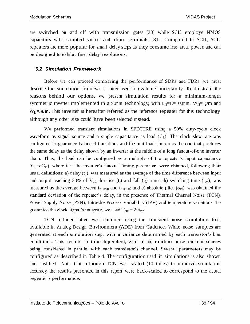
and step (Tn). In Fig. 17a, we show the impact of different PSN levels on jitter insertion, for
a FO4 inverter with Tn=Tclk and Tn=4Tclk. It shows that jitter grows almost linearly with
PSN standard deviation (σpsn) if it is small (< 10%Vdd), and exponentially if it is higher.
Hereafter we will consider only small PSN levels, as it is the most common scenario in
well designed Integrated Circuits (ICs). Thus, jitter can be considered to depend linearly
on PSN magnitude, as is usually observed in practice [33]. In Fig. 17b, jitter is shown as
a function of the noise cut-off frequency (fn=1/Tn). It shows a resonance peak for fn=fclk
and again for fn=2fclk. In contrast, for fn<<fclk, jitter is almost constant. Because PSN is
usually considered to have a low-frequency spectrum compared to the clock frequency,
we will also hereafter assume fn=0.25fclk.
In general, the run length of a transient simulation depends on the system nature. In a
terminating system, the duration of the simulation is fixed by specification or by an event
definition that marks the end of the simulation. The simulation goal is to understand system
Table 4: Transient noise analysis: configuration parameters.
Parameter Description Value Justification
noisefmax
Bandwidth of pseudo random
noise sources. A non-zero value
turns on the noise sources during
transient analysis.
0.5 p (1)
This is the knee frequency for typical
digital signal shapes, which is not too
far beyond the inverter ’s intrinsic -
3dB bandwidth [32].
noisescale noise scale factor applied to all
generated noise. 10
This gain used to artificially inflate
the small TCN and make it visible,
above transient analysis numerical
noise floor.
noiseseed Seed for the random number
generator. 1
We use the same seed across
simulations, to compare the repeater
’s performances under the same
circumstances.
noisefmin
Power spectral density (PSD)
of noise sources depend on
frequency in the interval from
noisefmin to noisefmax.
noisefmax
(default)
In this case, only white noise is
considered.
noisetmin Time interval between noise
source updates.
1/noisefmax
(default)
Smaller values would produce
smoother noise signals, but would
reduce time integration step.
(*) p is the repeater’s parasitic delay.
Modulation Schemes VIDAS Project
Instituto de Telecomunicações – Pólo de Aveiro 38 / 94
behaviour for a typical fixed duration. On the other hand, a non-terminating system is in
perpetual operation and the goal is to understand its steady-state behaviour. In the present case,
the system is non-terminating unless we specify an event to mark the end of simulation. If jitter
could be calculated during the simulation run, the event could be the time instant for which a
given confidence level was reached for the chosen performance metric. Unfortunately, absolute
jitter can only be calculated after the simulation run and thus, a fixed simulation time (Tsim) had
to be imposed. Because the accuracy of the sample standard deviation is directly proportional to
sample size, we can only reach a reasonable value for Tsim by inspection of simulation results.
Figures 18a and 18b show the inverter’s TCN and PSN jitter evolution for growing
sample sizes (N=Tsim/Tclk). Both have shown to follow inverse exponential functions towards a
reasonable constant final value. However, PSN jitter took a much longer simulation time to do
that. To have accurate results within a reasonable simulation time, the simulation run length was
set to one thousand clock cycles for TCN jitter (N=1000) and three thousand for PSN jitter
(N=3000). IPV jitter was evaluated with Monte Carlo (MC) simulations, which also usually
requires thousands of simulation steps until enough delay values are obtained. Fortunately,
screening experiments have shown that a reasonable number of runs could be used in such
simple structures as clock repeaters. Fig. 18c shows IPV jitter in the reference repeater for an
increasing number of runs and the correspondent simulation time penalty (simulation time
compared to the time needed for 50 runs). A good compromise between accuracy and simulation
time was found to be around 200 runs.
Jitter simulations results are shown in Fig. 19a for a balanced reference repeater, with
σpsn=10%Vdd and increasing fanouts (FoN, N=1..6). Jitter is shown to increase linearly with
fanout for all sources, but with different rates. For this fanout range TCN jitter increased 1.1
Fig. 17: PSN jitter in the reference FO4 inverter, for different: a) noise levels (σpsn/Vdd); and b) cut-off
frequencies (fn).

Modulation Schemes VIDAS Project
Instituto de Telecomunicações – Pólo de Aveiro 39 / 94
times, while PSN and IPV jitter increased 3.2 times and 2.6 times, respectively. TCN jitter grows
slowly with fanout because the high-frequency noise components are affected by the low-pass
filtering imposed by CL. It is also shown to be much smaller (one order of magnitude) than PSN
or IPV jitter. Yet, TCN jitter will not be neglected as it represents a fundamental limit on
dynamic timing precision. On the contrary, PSN and IPV jitter have the same order of
magnitude for σpsn10%Vdd.
Furthermore, to observe the impact of different noise modes, we repeated PSN jitter
simulations using random noise sources in power and ground rails, in different configurations.
Fig. 19b shows that jitter induced by CMN sources is higher than for DMN sources, while jitter
induced by MMN sources (independent noise sources in power and ground rails) falls between
CMN and DMN bounds. MMN jitter is around 35% lower than CMN jitter and 35% higher than
Fig. 18: a) TCN jitter vs. N; b) PSN jitter vs. N; c) IPV jitter vs. MC runs. The elapsed simulation time
reference is the time taken to perform 50 runs (reference value).
Fig. 19: Jitter in the reference inverter, for different fanouts and: a) PSN, TCN and IPV sources; b) CMN,
DMN and MMN sources.

Modulation Schemes VIDAS Project
Instituto de Telecomunicações – Pólo de Aveiro 40 / 94
DMN, considering that all sources have the same noise power (σdmn=σcmn=σmmn). For simplicity,
we hereafter consider PSN sources to be arranged in a MMN configuration, unless otherwise
noticed.
The impact of temperature on PSN, TCN and IPV jitter was also investigated. Results are
presented in Fig. 20a, for an FO4 inverter with 0ºCT100ºC, with values normalized to jitter
measured at room temperature (T=27ºC). As expected, temperature has a significant impact on
TCN jitter. We measured a variation of 21% in TCN jitter values, for the specified temperature
range. On the contrary, PSN and IPV jitter varied less than 5%. Because these sources are
usually more relevant than TCN, temperature can be considered a marginal jitter source in most
applications. Moreover, temperature variations can be easily mitigated using deskewing
schemes.
In Fig. 20b we evaluate the FO4 inverter’s performance for unbalanced transitions. We
can see that when tintout, jitter is not very much affected by the input transition time. On the
contrary, it increases fast when tin>tout, following the typical output transition time behaviour
under fast and slow input transitions [34]. Thus, a good design practice to achieve low clock
uncertainty is to keep balanced transitions in clock repeaters. However, if clock repeaters have
internal unbalanced cells (like tapered buffers or TDRs), their performance is inevitably affected
by this effect. For example, in a tapered buffer with high ζ, the smaller jitter generated in the first
inverter (with fast input transitions) will not fully compensate for the higher jitter generated in
the second cell (which has slower input transitions). This effect will also have a significant
impact on Crosstalk (CRT) jitter, because the load variations induced by crosstalk have the side
effect of unbalancing transitions in otherwise balanced cells.
Fig. 20: Jitter in the FO4 reference inverter, for: a) different operating temperatures; b) unbalanced
transition times.

Modulation Schemes VIDAS Project
Instituto de Telecomunicações – Pólo de Aveiro 41 / 94
5.3 Performance Analysis
In this section we evaluate the performance of SDRs and TDRs, using the simulation
framework described for the reference inverter. Results are presented for σpsn=6%Vdd, Tn=4Tclk,
T=27ºC and tin=tout. In Table 5, we compare timing, precision, area and power metrics. Because
SDRs have different nominal delays, we use both jitter and delay uncertainty (jitter as a
percentage of propagation delay) as precision metrics. Also, we performed circuit simulation
only, as different layout styles could influence the results. Implementation area values are given
in terms of logical squares (Lsq), which correspond to units of a minimum-size NMOS transistor
in this technology (Ln=100nm and Wn=120nm). Power corresponds to the average power
consumed per clock cycle, with Tclk=500MHz.
For each SDR, the table presents simulation results for fanout-of-one (FO1) and fanout-
of-four (FO4) repeaters. It also includes results for an FO16 buffer with =4, in which inverters
have balanced transitions (both are FO4 inverters). A higher fanout corresponds to higher jitter,
delay, transition times and power in all repeaters. However, when these cells are used to insert a
given amount of delay, precision is best evaluated with the uncertainty metric. If this is the case,
a higher fanout increases PSN uncertainty and decreases both TCN and IPV uncertainty. This
results from the fact that PSN is essentially low-pass and thus, it is not affected by the repeater’s
bandwidth (partially determined by CL).
Regarding different topologies, SEC inverters are shown to have a better timing
performance than symmetric inverters (especially the Invf), at the cost of higher power
consumption. Comparing buffers with inverters, we can see that although inverters have lower
absolute jitter, dynamic uncertainty is smaller in buffers. Also, uncertainty is smaller in buffers
Table 5: SDR performance metrics with σpsn=6%Vdd
SDR Time [35] Jitter [35] Uncertainty [%] Power Area
td tsw PSN TCN IPV PSN TCN IPV [uW] [Lsq]
Inv FO1 14 16 1.30 0.023 0.75 9.02 0.159 5.21 5.40
33.4 FO4 39 49 3.54 0.039 1.92 9.20 0.102 4.98 14.5
SEC
Invr
FO1 11 14 1.04 0.014 0.71 8.44 0.126 6.27 33.0 33.4
FO4 31 42 2.80 0.026 1.94 9.15 0.087 6.35 29.4
SEC
Invf
FO1 7 7 0.57 0.007 0.28 8.23 0.116 4.26 33.0 33.4
FO4 17 20 1.52 0.016 0.70 8.84 0.093 4.07 29.4
NAND FO1 20 24 1.94 0.027 1.14 9.61 0.138 5.80 7.70
83.3 FO4 47 62 4.60 0.045 2.75 9.75 0.095 5.83 18.7
Buffer
=1
FO1 29 18 2.00 0.038 1.62 6.89 0.132 5.63 10.9 66.7
FO4 52 47 3.79 0.056 2.77 7.33 0.108 5.35 19.9
Buffer
=4
FO1 42 21 2.84 0.046 2.75 6.78 0.109 6.55 26.0
166.7 FO4 50 27 3.28 0.048 3.08 6.58 0.096 6.18 35.5
FO16 75 55 4.88 0.057 4.10 6.51 0.076 5.47 72.4

Modulation Schemes VIDAS Project
Instituto de Telecomunicações – Pólo de Aveiro 42 / 94
with higher values. This means that for the same total delay, tapered buffers are less affected
by PSN and TCN than inverters. Regarding the impact of fanout on PSN jitter, tapered buffers
behave differently from single gate repeaters, because internal gates are balanced only for a
fanout equal to 2. For other fanouts, unbalanced transitions result in higher jitter insertion.
The NAND gate repeater seems to have no significant advantage compared to the
inverter, because its most important feature is not evident. The NAND gate has the benefit to
provide two point-of-entry control signals which can be used to build compact DCDLs. For that
particular application, inverter/buffer based SDRs have to be associated to a multiplexer, which
increases the fanout of each cell and introduces more uncertainty. This means that the fanout of
one NAND gate should be compared to an FO3 or FO4 inverter, depending on the multiplexer
design. In this case, NAND repeaters are a good alternative to inverter/buffer based SDRs with
the disadvantage of having a higher minimum delay.
The performance of different TDRs was also compared, using 90nm simulation results.
The repeater’s design followed the configuration shown in Fig. 16, where inverters correspond to
reference repeaters. To allow a fair comparison, TDRs were designed to have similar maximum
and minimum delays. In SCI2 and CSI repeaters, we used transistor sizing. However, due to the
charge-sharing effect, this technique could not be used in VRI and SCI1 repeaters. In these
repeaters we introduced extra static NMOS capacitances at the output of the first inverter to
compensate for their lower minimum delay. Table 6 shows the size of transistors used in the
controlling structures of each TDR (please refer to Fig. 16). In the SCI1 repeater, transmission
gates (TGi) are used to control the bank of NMOS capacitances (Mi). Transistors M3-M4, M5-
M6 and M7-M8 correspond to TG0, TG1 and TG2, respectively. Transistor M9 corresponds
to the extra static NMOS capacitance used in the VRI and SCI1 repeaters.
In Table 7 we present the same performance metrics shown for SDRs, for maximum and
minimum input vectors (maximum and minimum delays). SCI cells show the best jitter and
uncertainty performance, at the cost of higher implementation area. As expected, both the VRI
Table 6: Transistor sizes in TDRs, following the structures in Fig. 16
Rep. Size
[nm] M0 M1 M2 M3 M4 M5 M6 M7 M8 M9
CSI L 700 700 700 100 100 100 100 100 330
W 1320 660 330 330 1000 1000 330 330 330
VRI L 1000 500 500 120 300 700 700 1400 1000
W 750 750 1500 750 250 500 250 250 1200
SCI1 L 2000 2000 2000 100 100 100 100 100 100 2000
W 700 1400 2800 700 700 1400 1400 2800 2800 2000
SCI2 L 2000 2000 2000
W 700 1400 2800

Modulation Schemes VIDAS Project
Instituto de Telecomunicações – Pólo de Aveiro 43 / 94
and the CSI are more sensitive to variations because delay is controlled by resistive paths in both
architectures. To increase the CSI robustness, authors in [29] proposed an alternative design
where the controlling transistors are replaced by current sources. Although this effectively
reduces the repeater’s sensitivity to PVT variations, it further increases its power consumption.
In respect to PSN, SCI1 performs better for large delays while SCI2 is better for small delays. It
is also interesting to notice that transmission gates in SCI1 introduce a resistive path to the load
capacitances, which reduces jitter insertion for large delays. In fact, this is the only cell for which
uncertainty decreases with increasing delay. Thus, for the purpose of inserting large delays with
low uncertainty, this is the most suitable TDR.
The repeater’s delay and power consumption is shown in Fig. 21, for all possible input
vectors. The SCI2 repeater is the one with higher delay linearity, with reasonable power
consumption. VRIs consume low and constant power, but are not very linear with the input
vector. Moreover, they have to be carefully designed due to the charge-sharing effect. The
impact of charge-sharing is also observable in the SCI1 repeater delay, when the largest
controlling transistor is turned on (b2 = 1). Although easy to design [36], the CSI exhibited the
worst power consumption of all TDRs, specially for small delays.
At this point, we can draw two important conclusions related to uncertainty in clock
repeaters. First, simulation results show that absolute jitter increases for higher fanouts in SDRs,
and higher input vectors in TDRs. However, gate delay seams to increase almost by the same
amount, which reduces the uncertainty variability in each structure (at least for the most
significant jitter sources, PSN and IPV). This means that uncertainty cannot be significantly
reduced by manipulating the repeater’s fanout. Second, except for the CSI repeater, results show
that uncertainty variability is also small among SDRs and TDRs. The mean values for PSN, TCN
and IPV are 7.8%, 0.11% and 5.77% with standard deviations equal to 1.35%, 0.02% and 0.86%,
respectively. This means that for given latency and implementation technology, jitter introduced
by clock repeaters is almost independent from their particular design.
Table 7: TDR performance metrics with σpsn=6%Vdd
TDR Time [35] Jitter [35] Uncertainty [%] Power Area
b2b1b0 td tsw PSN TCN IPV PSN TCN IPV [uW] [Lsq]
SCI 000 113 50 16.9 0.343 8.8 15 0.303 7.8 216
229 111 183 78 31 0.704 17.9 16.9 0.385 9.8 114
VRI 000 105 48 8.7 0.127 6.3 8.2 0.121 5.9 20
410 111 195 77 17.5 0.257 11.9 9 0.131 6.1 21
SCI1 000 111 47 7.9 0.104 8.9 7.1 0.093 8.0 46
1298 111 196 79 10.8 0.181 10.8 5.5 0.092 5.5 129
SCI2 000 111 41 6.1 0.104 7.0 5.5 0.094 6.3 48
883 111 196 76 13.6 0.181 11.6 6.9 0.079 5.9 90

Modulation Schemes VIDAS Project
Instituto de Telecomunicações – Pólo de Aveiro 44 / 94
Fig. 21: Performance metrics for CSI, VRI, SCI1 and SCI2 repeaters, with respect to input vector (b2 b1
b0): a) delay; b) power consumption.

Modulation Schemes VIDAS Project
Instituto de Telecomunicações – Pólo de Aveiro 45 / 94
Section 6
6. Uncertainty in Cascaded Clock Repeaters
6.1 Digitally Controlled Delay Lines
Clock repeaters are typically used to distribute a clock signal to different locations or to
introduce controllable amounts of delay in a given clock path. The former is usually called a
Clock Distribution Network (CDN), while the last is generally referred to as a Delay Line (DL).
Apart from their purpose, the most significant difference between these structures is the electrical
and physical distance between repeater cells. In DLs, repeaters are located in close proximity so
interconnect parameters may be disregarded when analyzing the circuit’s operation. On the
contrary, interconnect parasitics cannot be neglected in CDNs. In this section we describe the
most common architectures of DLs and CDNs, and discuss the key parameters that influence
their precision.
When a clock signal travels through more than one repeater we say it travels through a
DL, which in its simplest form is just a cascade of SDRs. If the line is composed of inverters
with increasingly larger size we call it a tapered DL. This is a very common structure when a
small gate has to drive a large capacitive load. On the other hand, a DL may be needed when the
clock signal must be intentionally delayed to meet some timing specifications. In this case, if the
delay can be digitally controlled we have a DCDLs [37]. These systems will produce only
quantized delays, but have less noise sensitivity, larger tuning range and simpler control circuitry
than Analog Controlled Delay Lines (ACDLs).

Modulation Schemes VIDAS Project
Instituto de Telecomunicações – Pólo de Aveiro 46 / 94
Fig. 22: Uniform DCDLs, built with: a) inverter gates; b) NAND gates.
If each stage introduces a constant delay, the delay line is said to be uniform and the
control unit is typically a ring counter. This is usually the case when DCDLs are implemented
with SDRs in a single-path configuration, as shown in Fig. 22. The inverter is usually chosen for
its reduced insertion delay [20], but requires a multiplexer to control the number of stages
through which the signal travels. On the other hand, NAND gates have the benefit to provide two
point-of-entry control signals, which can be used instead of the multiplexer, and can be used to
build DLs with very regular layouts [38, 39]. Non-inverting SDRs, like buffers or AND gates,
are less popular because DCDLs are usually required to have the lowest unit delay possible.
When a large phase range and a reduced implementation area are required, delay stages
are usually implemented with weighted delays, controlled with a binary counter. This is typically
accomplished with SCIs or SDRs associated to multiplexers in a parallel-path configuration.
These structures are shown in Fig. 23. In parallel-path DCDLs, the unit delay is obtained from
the difference between the delay of alternative paths [21]. Due to their poor resolution, these
lines are typically used to implement coarse DLs while single stage SCIs are more interesting to
implement fine- tuning DLs. For large delays, multiple SCIs can be cascaded (as represented in
Fig. 23), at the cost of a higher minimum delay.
The number of delay elements in a inverter-based DL depends on the required total delay
(tD) and may be calculated using the Sakurai’s propagation delay and transition time expressions
[40]. Considering equal td,LH and td,HL and tin=tout, the total delay tD after N cells is shown in (71).
We can see that tD is proportional to the gate’s output capacitance, which results from the next
cell’s input capacitance and the multiplexer’s input capacitance. For large delays we can either
Fig. 23: Binary weighted DCDLs with: a) SCIs; b) SDRs in a parallel-path configuration

Modulation Schemes VIDAS Project
Instituto de Telecomunicações – Pólo de Aveiro 47 / 94
increase the number of cells or the load capacitance in each cell.
0 0
0
0.9 12 ln 0.5 1
2 0.8 0.8 1
L dd D i D i T
D d
d dd dd
C V V V vt N t N
I V eV
(71)
To have a good delay resolution and a large dynamic range in uniform DCDLs, we need
a large number of fast delay cells. Alternatively we can use a single stage SCI, with a shunt
capacitance M=N-1 times bigger than CL, saving area and power consumption. However, this
large capacitance may compromise slew-rate and increase the signal sensitivity to PSN. To take
the best out of both worlds, DCDLs often employ multiple stages of coarse and fine-tuning delay
cells with different structures. Coarse tuning is usually accomplished with uniform DLs for their
simplicity and predictability, while fine tuning is implemented with TDRs [39, 41, 42]. Fine
tuning can also be implemented with direct [43, 44] and feedback path phase blenders [45] or
variable strength drivers [18], which are not discussed here.
Regarding precision, uniform delay lines are usually seen as less accurate because jitter
accumulates along the line. However, several different phenomena should be accounted for when
analyzing jitter in these structures. Although jitter accumulation may be worse in long uniform
DLs (due to the large number of cascaded cells), SCIs are intrinsically unbalanced, which has
already been shown to have a detrimental effect on jitter. In the following section, jitter in
DCDLs is analyzed using simulation results.
6.2 Performance Analysis
Here, we evaluate the performance of DCDLs, using the simulation framework and gate
design techniques described before. In Table 8, we present time and precision metrics for
uniform and binary weighted DCDLs. The structures were implemented in a 90nm IBM
technology, and designed for the same maximum path delay (tDmax). The only exception is the
parallel-path (Pp) DCDLs, designed for twice the delay of other lines due to its large minimum
step. Timing metrics include delay resolution (d), maximum and minimum path delay (tDmax and
tDmin). Regarding precision metrics, the table shows results for TCN, IPV and PSN induced jitter
and uncertainty, measured at each DCDL output, with maximum delay selected, σpsn=6%Vdd,
Tn=4Tclk and T=27ºC. In PSN jitter evaluation, we used the same MMN sources for all cells, so
noise is totally correlated between stages but independent in power and ground rails.
We used an inverter-based DCDL with two different multiplexer configurations - one
using pass-transistor gates (PTmux) and another built with tri-state inverters (3STmux). Each
delay cell is loaded with the input capacitance of the next cell and the multiplexer’s input

Modulation Schemes VIDAS Project
Instituto de Telecomunicações – Pólo de Aveiro 48 / 94
capacitance. Because those multiplexers have different input capacitances, DLs have different
resolutions and a different number of cells for the same tDmax .PTmux DCDL includes fourteen
inverters while the 3STmux DCDL has only eight inverters. With less stages and heavier
multiplexer, the 3STmux DCDL’s dynamic range (∆= tDmax- tDmin) is also smaller. Regarding
precision, TCN jitter is smaller in the line with higher capacitive load because the repeater ’s
have lower noise bandwidths. On the contrary, PSN and IPV precision metrics have similar
values in both lines. Using NAND gates with the same output current as inverters, the DCDL
requires only four stages for the same tDmax . Compared to other uniform lines, it has a larger d
but also a larger ∆, because there is no need for an additional multiplexer (that introduces a delay
overhead). However, its jitter performance is very similar to inverter-based lines.
Results for a single stage SCI and a parallel-path DCDL are also shown. The parallel-
path DCDL has four binary weighted stages with tri-state inverter multiplexers, while the SCI is
controlled by four binary weighted capacitors in a type 2 configuration. The SCI has a smaller
delay step but very limited dynamic range. On the contrary, the parallel-path line has about twice
the dynamic range, with a delay resolution three times larger. Due to its larger tDmax, absolute
PSN and IPV jitter are also much larger than in other DCDLs but uncertainty remains quite
similar to values measured before. TCN jitter is the only precision metric that does not seem to
keep pace with delay and depends mostly on each cell’s noise bandwidth. Thus, lines with larger
capacitive load per cell have lower TCN jitter.
We have also observed that jitter and delay increase at similar rates, so uncertainty is
almost constant along uniform linear and for any delay in binary weighted lines. Also, PSN and
IPV uncertainty are almost constant regardless the DCDLs architecture. If we neglect TCN jitter
(which is much smaller than jitter induced by other sources), this means that jitter in DCDLs
depends only on tDmax, and not on their specific architecture.
Fig. 24, shows PSN jitter evolution in an 8-cell inverter DCDL for different PSN
magnitudes and bandwidths. As before, we selected the maximum line delay and applied the
same noise sources to all repeaters. Above each plot we show the line’s mean uncertainty
(average of uncertainty computed at the output of each cells) and standard deviation (µ and σ).
Table 8: DCDL performance metrics with σpsn=6%Vdd
Structure Time [35] Jitter [35] Uncertainty [%]
td TDmax tDmin PSN TCN IPV PSN TCN IPV
Inv DL Ptmux 15 289 92 26.4 0.34 19.8 9.13 0.12 6.86
3Stmux 25 288 114 26.8 0.15 19.2 9.33 0.05 6.67
NAND DL 69 276 69 29.6 0.18 18.6 10.7 0.07 6.76
Pp DL 3Stmux 23 585 247 52 0.23 36.4 8.64 0.04 6.05
SCI DL Type 2 8.1 297 175 28.1 0.19 14.2 9.5 0.06 4.8

Modulation Schemes VIDAS Project
Instituto de Telecomunicações – Pólo de Aveiro 49 / 94
We can conclude that PSN uncertainty is almost constant along the line (low standard deviation).
Also, its mean is shown to depend linearly on noise magnitude (υn) but is not very sensitive to
noise step, as long as Tn<Tclk. These observations allow us to write an expression for normalized
low-frequency PSN uncertainty, as shown in (72). This normalized PSN uncertainty is a constant
parameter for any DCDL, regardless its architecture or noise levels. It depends only on the
implementation technology.
,psn psn n td psn ddd d psnU V t (72)
Simulation results shown here allow us to take an important conclusion - both dynamic
and static uncertainties are constant for a given technology and thus, can be used to predict
precision in general DCDLs. This statement refers to IPV uncertainty (Uipv) and to the
normalized PSN uncertainty (psn). For a more complete characterization, we can also obtain
bounds for psn, using CMN and DMN sources.
Statistical accumulation models are frequently used to predict jitter accumulation, based
on individual jitter contributions. If jitter sources are uncorrelated, jitter after N cells is computed
by the sum of individual variances; if sources are totally correlated, jitter is results from the sum
of standard deviations. In uniform DCDLs, we considered that all elements are affected by the
same PSN sources (totally correlated noise sources). Thus, using that model we should be able to
compute output jitter based on each cell’s jitter contribution. IPV sources are also highly
correlated in these structures, due to the cell’s proximity. On the contrary, TCN jitter
contributions are intrinsically uncorrelated. Fig. 25 compares jitter simulation results with the
statistical model predictions, for the inverter based DCDL with tri-state inverter’s multiplexer.
Fig. 24: Jitter in inverter-based DCDL for different: a) PSN ratios (υn); and b) noise steps (Tn)

Modulation Schemes VIDAS Project
Instituto de Telecomunicações – Pólo de Aveiro 50 / 94
We can see that the statistical model provides reasonable accurate jitter predictions for
TCN, IPV and MMN jitter. However, if PSN sources are mainly DMN or CMN, the model fails
significantly. Later in this document, we propose a modified statistical accumulation model to
cope with different PSN modes and also to predict jitter accumulation when sources are not
totally correlated. Although this situation is not expected in DCDLs, due to the cell’s spatial
proximity, it is a reasonable assumption when repeaters are placed in distant locations, as in
clock distribution trees.
6.3 Clock Distribution Trees
Clock trees are the most commonly used structure used in CDNs. Although clock meshes
or clock grids are used in some designs, they are less preferred due to the high routing cost and
clock power. Clock trees are two dimensional structures with cascaded repeaters, intended to
connect a clock source to clocked units, scattered throughout a synchronous system. Because the
clock signal must travel long distances, clock repeaters generally include interconnects with
significant distributed resistance and capacitance. Inductance may also have a non-negligible
impact on the repeater delay, especially if wide and thick interconnects are used [46]. However,
its impact on clock distribution is usually not considered due to the added complexity overhead.
For the same reason, inductance will not be considered here.
A clock tree is synthesized from the positions and capacitance loads of the clock sinks. In
H-trees, the number of stages determines the number for clock repeaters from source to sink. In
Fig. 26a is represented an H-tree with three stages, i.e., with N=7 repeaters along the clock path.
If we consider a uniform load distribution (for simplicity), the total load driven by each sink can
Fig. 25: Jitter simulation results and statistical model predictions for: c) uncorrelated TCN sources; b)
totally correlated PSN sources; and c) strongly correlated IPV sources.

Modulation Schemes VIDAS Project
Instituto de Telecomunicações – Pólo de Aveiro 51 / 94
be easily found. Next, the length of each branch is computed given the chip size and tree stages.
Their width depends on the selected wire sizing technique, which can be: a) uniform, and all
wires have the same width; or b) geometric, and the widths are geometrically increased from sink
to source. Fig. 26b represents a two stage H-tree with geometric wire sizing.
For a given branch i, we can approximately calculate interconnect capacitance (Cint) and
resistance (Rint) as shown in (73). Here, R is the resistance, Cc is the coupling capacitance and Cg
is the capacitance to ground in a nominal width interconnect, w is the wire width ratio to the
nominal width and L is the wire length. Once the interconnect parasitics are determined, the size
of each repeater can be obtained for a given performance specification. In clock tree design,
skew is usually the key performance parameter to minimize, so latency should be reduced as
much as possible. It is known that the delay of a cascaded driver, driving a large load, becomes
minimum when CL/Cin=e. However, the trade-off between power and skew often imposes lower
limits on rc and thus, on repeater sizing [47].
int, int2
i c g i i i iC C C w L R R L w (73)
For generic clock trees and non-uniform load distribution, tree design is not so straight-
forward and Clock Tree Synthesis (CTS) tools are needed to meet specifications. The first step is
topology generation through partitioning the clock sinks, followed by routing and optimization
steps. In the past, the primary job of CTS tools was to vary routing paths, placement of the
clocked cells and clock buffers to meet maximum skew specifications [48]. The clock tree
quality depended on how well the designer could balance the clock paths in order to mitigate the
delay penalty introduced by skew. Moreover, he could trade-off power and area for timing if
higher operation speed was needed, using bigger clock repeaters. These traditional specifications
Fig. 26: H-trees: a) three stages and uniform wire sizing; b) two stages and geometric wire sizing.

Modulation Schemes VIDAS Project
Instituto de Telecomunicações – Pólo de Aveiro 52 / 94
are enumerated next.
power consumption - clock trees consume a significant portion of the total chip power
since it has the highest activity factor and drives the largest capacitive load in
synchronous integrated systems. It is important to minimize its size, not only for power
saving concerns but also for temperature and PSN;
implementation area - implementation area is not always available for free in a given
location. Increasing the repeater ’s size may be costly (if circuit blocks must be replaced
and/or rerouted) or even not possible;
routing resources - the clock net is one of the largest nets in a synchronous design and is
usually designed along with shields to minimize crosstalk. Because it is one of the first
nets to be routed, it constitutes a blockage for other nets and thus, its routing area should
be minimized;
insertion delay - uncertainty is roughly proportional to path delay, so the tree insertion
delay should be minimized;
transition times - recommended rise/fall transition time is less than 10% of clock cycle.
While sharp transition times are critical for high speed operation and robustness to PVT
variations, it typically increases power consumption and PSN;
clock skew - since skew represents a cycle-time penalty, it’s important to minimize it in
order to enable maximum operating frequency. Although controllable amounts of skew
can be intentionally introduced to optimize the circuit’s performance (clock skew
scheduling), it is generally considered as an unintentional and undesirable difference in
clock arrival times, due to load, interconnect and device mismatches in the clock tree;
Now-a-days, designing CDNs for high-speed systems is more complex than just meeting
skew specifications. To ensure reliability, recommended jitter is usually less than 10% of clock
cycle, which is not always easy to guarantee given the ever increasing on-chip PVT variations.
Several works have shown that trees with a small number of large repeaters with wide
interconnects between them are more robust to variability sources and also guarantee sharp
transitions [49, 50], which are helpful in minimizing jitter [51]. Also, parameter variation effects
on the final levels of an H-tree have a higher impact on performance than those on the first tree
level [52]. However, none of these works give the designer an insight regarding the jitter
accumulation mechanism in clock trees and the impact of correlations between jitter sources.
Modern packaging styles and techniques to reduce power consumption have changed the typical

Modulation Schemes VIDAS Project
Instituto de Telecomunicações – Pólo de Aveiro 53 / 94
noise modes and correlations, so further investigation is required to understand those
mechanisms.

Modulation Schemes VIDAS Project
Instituto de Telecomunicações – Pólo de Aveiro 54 / 94
Section 7
7. Jitter Accumulation Model
In this section we analyze the mechanism behind dynamic jitter accumulation in Clock
Repeater Cells (CRCs) and discuss the impact of jitter amplification, according to power/ground
noise correlations and correlations among noise sources in cascaded repeaters. Static jitter
accumulation is not discussed because the traditional statistical accumulation models are
generally accepted as good estimators for static jitter [53].
7.1 Dynamic Jitter in Cascaded Repeaters
In cascaded clock repeaters, jitter associated to a clock path depends on jitter generated
by each CRC on that path. CRCs are usually designed to exhibit similar input and output
transition times, so a given clock path can be represented by a cascade of balanced CRCs (with
similar rc=Cout/Cin and rio=tin/tout=1). In Fig. 27, we represent such a general clock path with N
equivalent CRCs affected by PSN sources. Here, σtd,i is the total jitter observed at the output of
cell i, which is different from the jitter inserted by cell i (σtd,ii), due to jitter amplification and
accumulation.
To explain the physical mechanism behind jitter amplification, we present here the results
of a simple experiment with three cascaded CRCs. We varied the supply and ground levels on
the first cell and compared the waveforms along that line (vni) with the wave-forms of a
reference line (vri), with nominal supply and ground levels. Fig. 28 shows the waveforms for

Modulation Schemes VIDAS Project
Instituto de Telecomunicações – Pólo de Aveiro 55 / 94
CMN and DMN, where ∆td,i is the instantaneous delay error observed at the output of cell i.
Similar results could be obtained for ∆vdd>0. Note that absolute jitter is by definition the
standard deviation of ∆td,i.
The graphics show that for both CMN and DMN, the instantaneous delay error
introduced by the first cell is transferred to the second cell with gain. This gain results from the
fact that the second cell’s input voltage is different from its supply voltage, which affects its
response to the input transition. After the second cell, the delay error does not increase because
there is no further influence of PSN sources (applied to the first cell only). Thus, the gain for
uncorrelated PSN sources (gu) depends on the relative position between the noisy CRC and the
observed cell. It has also been shown to be higher for DMN than for CMN and depend on the
CRC design parameters, as will be discussed latter in this section.
Fig. 27: Cascaded CRCs and their output jitter
Fig. 28: Waveforms of a reference CRC line (vri) and a CRC line affected with PSN in the first cell only
(vni) for: a) CMN; b) DMN

Modulation Schemes VIDAS Project
Instituto de Telecomunicações – Pólo de Aveiro 56 / 94
A second experiment was performed to observe jitter gain when CRCs have totally
correlated PSN sources. We used the same repeater line, but now all cells share the same power
and ground levels. The resulting waveforms are shown in Fig. 29 for ∆vdd<0, but similar results
could be obtained for ∆vdd>0. We can see that the instantaneous delay error measured at the
second cell is not twice the error measured in the first cell, as we would expect in a cascade of
identical cells with correlated noise sources. For CMN, the amplification gain is even negative
(attenuation), which almost mitigates jitter accumulation. This negative effect of CMN in
cascaded inverters has also been observed in [54]. On the contrary, DMN causes significant jitter
amplification as all contributions have a positive effect on jitter accumulation. The gain for
correlated sources (gc) is thus different from g
u, although it also depends on the noise mode and
CRC design parameters.
7.2 Bounds for Jitter Accumulation
If PSN sources are uncorrelated in each CRC, we can use the superposition principle and
an amplification gain parameter to estimate jitter along the line, as shown in (74). The gain
elements define a lower triangular matrix [gu] with gij
u=0, for j>i and gij
u=1, for j=i. Each
element giju is the gain applicable to jitter generated in cell j in order to obtain its contribution to
jitter in cell i. Note that we sum jitter variances because jitter contributions from uncorrelated
sources are independent random variables (the superscript u stands for uncorrelated). To obtain
the individual estimates σtd,ii, we can use a scalable jitter model [55] or rely on simulation results
performed for each CRC [53].
Fig. 29: Waveforms of a reference CRC line (vri ) and a CRC line with the same PSN sources in all
cells (vni ) for: a) CMN; b) DMN.

Modulation Schemes VIDAS Project
Instituto de Telecomunicações – Pólo de Aveiro 57 / 94
2 2 2
, ,1 1
u u u
td i td iiN N N N
g
(74)
If PSN sources are totally correlated, we cannot use the superposition principle. In this
case, the dynamic jitter after N cells depends on the sum of individual standard deviations and on
the gain for totally correlated sources. In (75) we show the expression to compute dynamic jitter
at the output of cell k in a cascade of N cells. The superscript c indicates the assumption of
correlated PSN sources.
, ,
1 11
k
c c c
td i td iiN N
i
g
(75)
In a general clock path, the amplification gain depends on many different design and
noise parameters, and is associated with the repeater’s non-linear behavior during the signal
transition. Thus, it is not straightforward to derive an accurate analytical model for [gu] and [g
c].
Instead, we propose a heuristic method based on the characterization of a reference repeater line
with N=5 similar CRCs. Screening experiments revealed that this is a sufficient number of cells
to provide an accurate characterization.
For uncorrelated PSN sources, the amplification gain can be obtained with transient noise
simulations with PSN applied to the first cell only. This can be done because gu depends only on
the relative position between the noisy CRC and the observed cell. We used MATLAB to
generate a set of power and ground noise samples (with the same standard deviation σvn), which
were imported into SPECTRE as piece-wise linear files in CMN and DMN configurations.
Simulations were repeated for different noise modes, noise variances and CRC design
parameters (rc and rr=Ron/Rint). Results were then used to obtain the gain elements (giju),
computed as the ratio between jitter measured at the output of cell i and jitter generated in the
first cell (j=1), as shown in (76).
, ,
1, ..., 1u u u
ij td i td jjg i N j (76)
For correlated PSN sources, the amplification gain elements (gic) can be obtained with a
similar procedure, but with the same PSN sources applied to all CRCs in the line. They are
computed as the ratio between the jitter measured at the output of each cell and the total expected
jitter at that node. In this case, the expectable jitter at the output of cell N is just N times the jitter
observed at the first cell (77).
, ,11, ...,
c c c
i td i tdg i i N (77)

Modulation Schemes VIDAS Project
Instituto de Telecomunicações – Pólo de Aveiro 58 / 94
Results can then be arranged in look-up tables or fitted into polynomial expressions. For
uncorrelated PSN sources, the gain elements depend on the noise mode, the noise standard
deviation as a percentage of the supply voltage (νn= σvn/Vdd), the design parameters (rc and rr)
and the relative position between the observed cell and the noisy cell (M=i-j). If PSN sources are
totally correlated, the gain elements have the same dependencies but now the relative position M
is replaced by the number of cascaded cells (N).
7.3 Simulation Results
In this section we evaluate the accuracy of the proposed jitter accumulation model. Model
results are compared with simulation data, using a two stage symmetric H-tree implemented in a
90nm technology. The tree was designed using Scilab, assuming an uniform load distribution
and geometric wire sizing. Each clock path has five inverter-based CRCs, with rc=4. Jitter
accumulation along the tree was then evaluated with transient simulations, using low-frequency
noise sources with different modes, amplitudes and correlations along the clock paths. Low-
frequency means that the noise cut-off frequency (fn) is much lower than the clock frequency
(fn=0.25fclk).
Following the procedure previously described, we obtained the repeater’s gain functions.
Results are shown in Fig. 30 for gk1u and gk
c, for k=1,...,5. For uncorrelated noise sources, jitter
amplification is shown to be almost constant after the second cell and is higher for DMN than for
CMN. The most relevant design parameter is shown to be rr, which significantly reduces jitter
accumulation. This means that Rint is beneficial for jitter accumulation when PSN sources are
uncorrelated. When noise sources are correlated, rr also has a beneficial impact on DMN jitter
accumulation but the most relevant parameter is shown to be noise amplitude (νn). On the
contrary, jitter gain for CMN is shown to be very small (<<1) and depend almost exclusively on
Fig. 30: Jitter gain for A (νn=5%, rc=2, rr=0), B (νn=5%, rc=10, rr=1), C (νn=5%, rc=8, rr=0) and D
(νn=10%, rc=8, rr= 0), for: a) uncorrelated noise sources; and b) correlated noise sources

Modulation Schemes VIDAS Project
Instituto de Telecomunicações – Pólo de Aveiro 59 / 94
the number of cascaded cells. Note also that rc does not have a significant influence on gain,
except for DMN when sources are correlated.
In Fig. 31 we compare simulation results with model predictions, for uncorrelated and
totally correlated PSN sources. Each plot shows the results for CMN, DMN and MMN sources,
with νn=3%. These plots show that the proposed model can predict jitter accumulation bounds
with good accuracy. This accuracy is graphically represented in Fig. 32, with x-y plots. The x-
axis corresponds to model predictions while the y-axis corresponds to simulation results. We
can see that jitter is well estimated, with most points falling above the 45 degrees line. The
model error, calculated as a percentage of the simulation results, is shown to be inferior to
10%. Note that individual jitter estimates were obtained using a scalable jitter model [55],
which also contributes to this final prediction error.
The model was further used to predict jitter in clock trees, designed with variable
Fig. 31: Dynamic jitter model predictions compared to simulation results, for: a) uncorrelated noise
sources; and b) correlated noise sources
Fig. 32: Model accuracy for a clock tree with five stages, rc= 4 and: a) uncorrelated noise sources; and b)
correlated noise sources.

Modulation Schemes VIDAS Project
Instituto de Telecomunicações – Pólo de Aveiro 60 / 94
interconnect parameters (Cint and Rint), wire sizing techniques (geometric or uniform) and chip
sizes. As it is not practical to graphically represent the results for all of these experiments, the
model accuracy is shown with x-y plots in Fig. 33. These results were obtained for uncorrelated
MMN sources and H-trees with two (N=5) and three stages (N=7). Jitter is shown to be well
estimated, with most points falling on the 45 degrees line and an error inferior to 10% in all the
experiments.
Although this may seem a large error, the proposed model is much more accurate than the
conventional and very popular statistical accumulation model. In Fig. 34 we compare simulation
results with predictions obtained with the conventional model. The plots show the error
computed as the difference between statistical model predictions and simulation results, as a
percentage of simulation results. We can see that the conventional statistical model fails to
predict dynamic jitter accumulation in most situations. When noise sources are uncorrelated, the
model (sum of variances) follows the same trends shown by simulation results, but
underestimates jitter with an error around 40% after only five clock repeaters. Yet, when noise
sources are totally correlated, it provides even worse predictions (sum of standard deviations).
For CMN, jitter is considered to accumulate very fast disregarding the positive effect of CMN. In
this case, the error is big and non-monotonic. It is also significant for DMN and MMN, with
dmn50% and mmn15% after only five CRCs.
The proposed jitter bounds can also be useful to highlight the implications of noise
correlations in jitter accumulation. They show that DMN is beneficial for jitter accumulation
only if noise sources in adjacent repeaters are uncorrelated. Circuits with wire-bonded packages,
usually have symmetric power and ground noise variations (dominant DMN). However, most
PSN in wire-bonded packages is low-frequency and highly spatially correlated [56]. Thus, jitter
Fig. 33: Model accuracy for different interconnect parameters, wire sizing techniques, chip sizes and: a)
two stages (N=5); and b) three stages (N=7)

Modulation Schemes VIDAS Project
Instituto de Telecomunicações – Pólo de Aveiro 61 / 94
accumulation can only be reduced if noise sources can be decorrelated, using dithering or similar
techniques.
On the contrary, for low inductance packages, DMN is dominant only if cascaded
repeaters share the same local power distribution parasitics. In this case, noise sources are
probably also highly correlated and jitter accumulates fast. However, if clock repeaters are
placed in different power blocks, DMN may no longer be dominant. This is beneficial for jitter
accumulation if noise sources are correlated in adjacent repeaters, but detrimental if they are
independent. In this scenario (repeaters in different power blocks), noise sources are not
expected to be totally correlated and we cannot take full advantage of the beneficial impact of
CMN. Nevertheless, we believe that this approach can result in a positive net effect because the
beneficial impact of CMN for correlated sources is by far more significant than its detrimental
effect for uncorrelated sources. Also, this difference becomes more pronounced with the number
of cascaded repeaters.
Fig. 34: Error between traditional statistical accumulation jitter predictions and simulation results, for: a)
uncorrelated noise sources; and b) correlated noise sources

Modulation Schemes VIDAS Project
Instituto de Telecomunicações – Pólo de Aveiro 62 / 94
Section 8
8. Performance Results
In this section we analyze the performance of DSSS SIK modulation system described
previously. We justify the use and benefits of using DSSS systems. We also compare its
performance with various other modulation techniques.
A BER of 10-6
is an acceptable value for stable data communication. This corresponds to
an approximate SNR of 13.5 dB for OOK. The simulation parameters for the configuration used
in the study are also shown in Table 1. Fig. 35 shows the BER performance of all modulation
techniques. While performance of L-PPM and OOK is nearly the same, I-PPM performs inferior.
But DSSS-SIK performs better than LPPM and I-LPPM. In Fig. 36, the required power to
maintain acceptable BER of 10-6
for modulation techniques is illustrated. L-PPM is considered to
be power efficient, however signal power requirement increases with the data rate.
One of the main characteristic of DSSS system is the processing gain which makes the
system reliable in noisy (interference) environment. Fig.37 shows the BER of DSSS SIK system
as a function of signal-to-interference (SINR=Pf/P) ratio. It can be seen that performance
deteriorates for smaller values of SINR.

Modulation Schemes VIDAS Project
Instituto de Telecomunicações – Pólo de Aveiro 63 / 94
Fig. 35: BER performance of different modulation schemes
Fig. 36: Necessary required power for different data rates to achieve BER of 10
-6

Modulation Schemes VIDAS Project
Instituto de Telecomunicações – Pólo de Aveiro 64 / 94
In this case a processing gain of 10 is considered for the fact that FPGA implemented
receiver is comparable. However, if the processing gain is increased, the receiver can tolerate
more interference. This is represented in Fig. 38. In this case, SINR varies from -30dB to 0dB
and PG is increased from 10 to 31. As we increase the PG, the BER performance of the system
increases.
Fig. 38: Performance of receiver when processing gain is increased and interference
ratio is varied from -30 to 0dB
Fig. 37: BER performance for different interference level

Modulation Schemes VIDAS Project
Instituto de Telecomunicações – Pólo de Aveiro 65 / 94
Fig. 39 illustrates the effect of noise variance on the system. Results in Fig. 40, Fig. 41
and Fig. 42 are based on Matlab Simulink model. Simulation environment and parameter settings
are shown in Table 1. The performance of two receiver architectures is shown in Fig. 40. It can
be seen that their performances are almost similar as both receiver architectures are optimum.
However, the computing time is higher in the case of integrate and dump correlator receiver.
Fig. 39: BER performance for different background noise
Fig. 40: Performance of two receiver architectures
1,0E-6
1,0E-5
1,0E-4
1,0E-3
1,0E-2
1,0E-1
1,0E+0
0 5 10 15
Bit
Err
or
Rat
e
Signal-to-Noise Ratio
BER Performance of Two Receiver Architectures
Integrate and Dump Receiver Architecture
FIR Receiver Architecture
1,25 pt
Modulation Schemes VIDAS Project
Instituto de Telecomunicações – Pólo de Aveiro 66 / 94
A comparison from OOK system of two receivers is also provided in Fig. 41. Fig. 42
illustrates the effect of non-LoS link on the channel. One strong non-direct path is considered
along with the LoS path. As shown, the performance of the receivers deteriorates. If the gain of
the indirect path increases, more SNR is needed to achieve the acceptable value of BER. The
effect of non-direct line on both the architectures remains the same.
Fig. 42: BER performance of SIK receiver with an additional delay path
Fig. 41: Performance comparison of Two Receiver Architectures with OOK
1.0E-7
1.0E-6
1.0E-5
1.0E-4
1.0E-3
1.0E-2
1.0E-1
1.0E+0
0 1 2 3 4 5 6 7 8 9 10 11 12
Bit
Err
or
Rat
e
Signal-to-Noise Ratio (dB)
Performance of receiver with one additional non-direct path
Channel with one non direct pathAWGN Channel
1,0E-7
1,0E-6
1,0E-5
1,0E-4
1,0E-3
1,0E-2
1,0E-1
1,0E+0
0 2 4 6 8 10 12 14
Bit E
rror
Rat
e
Signal-to-Noise Ratio (dB)
BER Performance of Two Receiver Architectures
Integrate and Dump Receiver ArchitectureFIR Receiver Architecture
OOK System

Modulation Schemes VIDAS Project
Instituto de Telecomunicações – Pólo de Aveiro 67 / 94
The performance of the receiver was then examined using additional noise sources on the
AWGN channel. This is considered to simulate different artificial light sources in the outdoor
environment. Though, in actual scenario the effect of such disturbances may not be uniform, a
range of value settings was considered. We used a uniform noise generator and examined the
effect of different values of noise. For example, Fig. 43 shows the effect of the noise from lower
bound of -0.25 to upper bound of 0.25, noise from lower bound of -0.35 to upper bound of 0.35
and also noise from lower bound of 0 to upper bound of 0.5. While the effect of negative and
positive values is uniform however, the effect of all positive noise produces non-uniform
behaviour especially towards lower BER.
Fig. 43: BER performance of receiver with additional interference
1.0E-6
1.0E-5
1.0E-4
1.0E-3
1.0E-2
1.0E-1
0 1 2 3 4 5 6 7 8 9 10 11
Bit
Err
or
Rat
e
Signal-to-Noise ratio (dB)
Performance of the Receiver of Simulink Model with additional Channel Noise
Uniform noise of lower bound -0.25 to 0.25
Uniform noise of lower bound -0.35 to 0.35
Uniform noise of lower bound -0.50 to 0.50
Uniform noise of lower bound 0 to 0.50

Modulation Schemes VIDAS Project
Instituto de Telecomunicações – Pólo de Aveiro 68 / 94
Section 9
9. Concluding Remarks
This report discussed and analyzed various modulation methods. The BER and SNR
performance parameters are discussed in detail for PPM and DSSS SIK techniques. Based upon
the simulation results, L-PPM which is a suitable method for IR do not provide significant
improvement in VLC systems. Therefore, a robust method based on DSSS SIK system is
developed and discussed for VLC systems. The performance of the system especially in road
safety applications in outdoor is expected to be improved using the technique of DSSS SIK.
Analytical as well as developed model in Matlab/Simulink performances are analyzed and results
are presented. It is observed that the DSSS SIK VLC systems perform better than pulse based
techniques unlike IR.

Modulation Schemes VIDAS Project
Instituto de Telecomunicações – Pólo de Aveiro 69 / 94
References
[1] A. J. C. Moreira, et al., "Modulation/Encoding Techniques for Wireless Infrared Transmission,"
Submission to the IEEE 802.11 Standardization Project, May 1993.
[2] M. D. Audeh and J. M. Kahn, "Performance evaluation of baseband OOK for wireless indoor
infrared LAN's operating at 100 Mb/s," Communications, IEEE Transactions on, vol. 43, pp.
2085-2094, 1995.
[3] S. Hidemitsu, et al., "Experimental Investigation of Modulation Method for Visible-Light
Communications," IEICE Trans Commun (Inst Electron Inf Commun Eng), vol. E89-B, pp. 3393-
3400, 2006.
[4] J. M. Kahn, et al., "Non-directed infrared links for high-capacity wireless LANs," Personal
Communications, IEEE, vol. 1, p. 12, 1994.
[5] M. Hoa Le, et al., "High-Speed Visible Light Communications Using Multiple-Resonant
Equalization," Photonics Technology Letters, IEEE, vol. 20, pp. 1243-1245, 2008.
[6] Z. Lubin, et al., "Improvement of Date Rate by using Equalization in an Indoor Visible Light
Communication System," in Circuits and Systems for Communications, 2008. ICCSC 2008. 4th
IEEE International Conference on, 2008, pp. 678-682.
[7] A. J. C. Moreira, et al., "Optical interference produced by artificial light," Wirel. Netw., vol. 3,
pp. 131-140, 1997.
[8] J. M. Kahn and J. R. Barry, "Wireless infrared communications," Proceedings of the IEEE, vol.
85, pp. 265-298, 1997.
[9] K.-C. Chen and T.-Y. Cheng, "Signalling Methods of IR PHY," Submission to the lEEE 802.11
Standardisation ProjectSept. 1993.
[10] F. R. Gfeller, et al., "Dynamic Cell Planning for Wireless Infrared In-House Data Transmission,"
presented at the International Zurich Seminar on Digital Communications, Zurich, Switzerland,
1994.
[11] M. K. Simon, et al., Spread Spectrum Communications Handbook, 1st ed., 2006.
[12] K. K. Wong, et al., "Infrared wireless communication using spread spectrum techniques,"
Optoelectronics, IEE Proceedings -, vol. 147, pp. 308-314, 2000.
[13] T. O'Farrell and M. Kiatweerasakul, "Performance of a spread spectrum infrared transmission
system under ambient light interference," in Personal, Indoor and Mobile Radio
Communications, 1998. The Ninth IEEE International Symposium on, 1998, pp. 703-707 vol.2.
[14] A. J. C. Moreira, et al., "Characterisation and modelling of artificial light interference in optical
wireless communication systems," in Personal, Indoor and Mobile Radio Communications, 1995.
PIMRC'95. 'Wireless: Merging onto the Information Superhighway'., Sixth IEEE International
Symposium on, 1995, pp. 326-331 vol.1.

Modulation Schemes VIDAS Project
Instituto de Telecomunicações – Pólo de Aveiro 70 / 94
[15] A. J. C. Moreira, et al., "Modulation methods for wireless infrared transmission systems -
Performance under ambient light noise and interference," presented at the Wireless Data
Transmission Conference - SPIE’s Photonics East Symposium, Philadephia, PA, USA, 1995.
[16] R. B. Watson, Jr. and R. B. Iknaian, "Clock buffer chip with multiple target automatic skew
compensation," Solid-State Circuits, IEEE Journal of, vol. 30, pp. 1267-1276, 1995.
[17] K. Shao-Ku, et al., "A 62.5–625-MHz Anti-Reset All-Digital Delay-Locked Loop,"
Circuits and Systems II: Express Briefs, IEEE Transactions on, vol. 54, pp. 566-570, 2007.
[18] C. Ching-Che and L. Chen-Yi, "An all-digital phase-locked loop for high-speed clock
generation," Solid-State Circuits, IEEE Journal of, vol. 38, pp. 347-351, 2003.
[19] C. Ching-Che and L. Chen-Yi, "A new DLL-based approach for all-digital multiphase clock
generation," Solid-State Circuits, IEEE Journal of, vol. 39, pp. 469-475, 2004.
[20] T. Matano, et al., "A 1-Gb/s/pin 512-Mb DDRII SDRAM using a digital DLL and a slew-rate-
controlled output buffer," Solid-State Circuits, IEEE Journal of, vol. 38, pp. 762-768, 2003.
[21] D. Guang-Kaai, et al., "Clock-deskew buffer using a SAR-controlled delay-locked loop," Solid-
State Circuits, IEEE Journal of, vol. 35, pp. 1128-1136, 2000.
[22] K. Jonghoon, et al., "Spread spectrum clock Generator with delay cell array to reduce
electromagnetic interference," Electromagnetic Compatibility, IEEE Transactions on, vol. 47, pp.
908-920, 2005.
[23] N. R. Mahapatra, et al., "An empirical and analytical comparison of delay elements and a new
delay element design," in VLSI, 2000. Proceedings. IEEE Computer Society Workshop on, 2000,
pp. 81-86.
[24] I. Sutherland, et al., Logical Effort: Designing Fast CMOS Circuits: Morgan Kaufmann, 1999.
[25] J. Mueller and R. Saleh, "A Tunable Clock Buffer for Intra-die PVT Compensation in Single-
Edge Clock (SEC) Distribution Networks," in Quality Electronic Design, 2008. ISQED 2008. 9th
International Symposium on, 2008, pp. 572-577.
[26] M. Saint-Laurent and M. Swaminathan, "A digitally adjustable resistor for path delay
characterization in high-frequency microprocessors," in Mixed-Signal Design, 2001. SSMSD.
2001 Southwest Symposium on, 2001, pp. 61-64.
[27] D. K. Jeong, et al., "Design of PLL-based clock generation circuits," Solid-State Circuits, IEEE
Journal of, vol. 22, pp. 255-261, 1987.
[28] M. Bazes, "A novel precision MOS synchronous delay line," Solid-State Circuits, IEEE Journal
of, vol. 20, pp. 1265-1271, 1985.
[29] M. Maymandi-Nejad and M. Sachdev, "A digitally programmable delay element: design and
analysis," Very Large Scale Integration (VLSI) Systems, IEEE Transactions on, vol. 11, pp. 871-
878, 2003.
[30] G. Geannopoulos and X. Dai, "An adaptive digital deskewing circuit for clock distribution
networks," in Solid-State Circuits Conference, 1998. Digest of Technical Papers. 1998 IEEE
International, 1998, pp. 400-401.
[31] P. Andreani, et al., "A Digitally Controlled Shunt Capacitor CMOS Delay Line," Analog
Integrated Circuits and Signal Processing, vol. 18, pp. 89-96, 1999.
[32] W. Maichen, Digital Timing Measurements: From Scopes and Probes to Timing and Jitter:
Springer Netherlands, 2006.
[33] K. Minami, et al., "A 1 GHz portable digital delay-locked loop with infinite phase capture
ranges," in Solid-State Circuits Conference, 2000. Digest of Technical Papers. ISSCC. 2000 IEEE
International, 2000, pp. 350-351, 469.

Modulation Schemes VIDAS Project
Instituto de Telecomunicações – Pólo de Aveiro 71 / 94
[34] P. Maurine, et al., "Transition time modeling in deep submicron CMOS," Computer-Aided
Design of Integrated Circuits and Systems, IEEE Transactions on, vol. 21, pp. 1352-1363, 2002.
[35] F. R. Gfeller and U. Bapst, "Wireless in-house data communication via diffuse infrared
radiation," Proceedings of the IEEE, vol. 67, pp. 1474-1486, 1979.
[36] M. Maymandi-Nejad and M. Sachdev, "A monotonic digitally controlled delay element," Solid-
State Circuits, IEEE Journal of, vol. 40, pp. 2212-2219, 2005.
[37] Y. Okajima, et al., "Digital Delay Locked Loop and Design Technique for High-Speed
Synchronous Interface (Special Issue on ULSI Memory Technology)," IEICE Transactions on
Electronics, vol. 79, pp. 798-807, 1996.
[38] L. Feng, et al., "A register-controlled symmetrical DLL for double-data-rate DRAM," Solid-State
Circuits, IEEE Journal of, vol. 34, pp. 565-568, 1999.
[39] R. J. Yang and S. I. Liu, "A 40-550 MHz Harmonic-Free All-Digital Delay-Locked Loop Using a
Variable SAR Algorithm," Solid-State Circuits, IEEE Journal of, vol. 42, pp. 361-373, 2007.
[40] T. Sakurai and A. R. Newton, "Alpha-power law MOSFET model and its applications to CMOS
inverter delay and other formulas," Solid-State Circuits, IEEE Journal of, vol. 25, pp. 584-594,
1990.
[41] C. Kwang-Hee, et al., "An Interpolating Digitally Controlled Oscillator for a Wide-Range All-
Digital PLL," Circuits and Systems I: Regular Papers, IEEE Transactions on, vol. 56, pp. 2055-
2063, 2009.
[42] C. Pao-Lung, et al., "A clock generator with cascaded dynamic frequency counting loops for
wide multiplication range applications," Solid-State Circuits, IEEE Journal of, vol. 41, pp. 1275-
1285, 2006.
[43] M. Byoung-Mo, et al., "Monotonic Wide-Range Digitally Controlled Oscillator Compensated for
Supply Voltage Variation," Circuits and Systems II: Express Briefs, IEEE Transactions on, vol.
55, pp. 1036-1040, 2008.
[44] B. W. Garlepp, et al., "A portable digital DLL for high-speed CMOS interface circuits," Solid-
State Circuits, IEEE Journal of, vol. 34, pp. 632-644, 1999.
[45] K. Mi-Jo and K. Lee-Sup, "100MHz-to–1GHz open-loop ADDLL with fast lock-time
for mobile applications," in Custom Integrated Circuits Conference (CICC), 2010 IEEE, 2010,
pp. 1-4.
[46] Y. I. Ismail, et al., "Exploiting the on-chip inductance in high-speed clock distribution networks,"
Very Large Scale Integration (VLSI) Systems, IEEE Transactions on, vol. 9, pp. 963-973, 2001.
[47] A. Chandrakasan, et al., Design of High-Performance Microprocessor Circuits: Wiley-IEEE
Press, 2000.
[48] E. G. Friedman, "Clock distribution networks in synchronous digital integrated circuits,"
Proceedings of the IEEE, vol. 89, pp. 665-692, 2001.
[49] J. Jinwook, et al., "Period Jitter Estimation in Global Clock Trees," in Signal Propagation on
Interconnects, 2008. SPI 2008. 12th IEEE Workshop on, 2008, pp. 1-4.
[50] D. C. Sekar, "Clock trees: differential or single ended?," in Quality of Electronic Design, 2005.
ISQED 2005. Sixth International Symposium on, 2005, pp. 548-553.
[51] M. Hashimoto, et al., "Statistical Analysis of Clock Skew Variation in H-Tree Structure," IEICE
Trans. Fundam. Electron. Commun. Comput. Sci., vol. E88-A, pp. 3375-3381, 2005.
[52] I. Chanodia and D. Velenis, "Parameter variations and crosstalk noise effects on high
performance H-tree clock distribution networks," Analog Integrated Circuits and Signal
Processing, vol. 56, pp. 13-21, 2008.

Modulation Schemes VIDAS Project
Instituto de Telecomunicações – Pólo de Aveiro 72 / 94
[53] V. Wason, et al., "An Efficient Uncertainty- and Skew-aware Methodology for Clock Tree
Synthesis and Analysis," in VLSI Design, 2007. Held jointly with 6th International Conference on
Embedded Systems., 20th International Conference on, 2007, pp. 271-277.
[54] L. H. Chen, et al., "Buffer delay change in the presence of power and ground noise," Very Large
Scale Integration (VLSI) Systems, IEEE Transactions on, vol. 11, pp. 461-473, 2003.
[55] M. Figueiredo and R. Aguiar, "Clock Repeater Characterization for Jitter-Aware Clock Tree
Synthesis," in Integrated Circuit and System Design. Power and Timing Modeling, Optimization
and Simulation. vol. 5953, J. Monteiro and R. van Leuken, Eds., ed: Springer Berlin / Heidelberg,
2010, pp. 46-55.
[56] K. Isaac and H. Chris, "Maximum Tolerable Power Supply Noise for Data-Clock
Synchronization," in Electrical Performance of Electronic Packaging, 2006 IEEE, 2006, pp. 167-
170.