visionsuper28' application board user's guide · 2016-02-09 · literature number:...
TRANSCRIPT

VisionSuper28 Vision Application Board
User's Guide
Literature Number: SPRUI53February 2016

2 SPRUI53–February 2016Submit Documentation Feedback
Copyright © 2016, Texas Instruments Incorporated
Table of Contents
Contents
1 Overview............................................................................................................................. 41.1 Vision Application Board ................................................................................................ 61.2 Features ................................................................................................................... 7
2 Hardware ............................................................................................................................ 82.1 Hardware Architecture................................................................................................... 8
3 Image Sensors Head Boards ................................................................................................. 93.1 Proprietary Image Sensor Head Board Interface .................................................................... 93.2 FPD-Link III FMC DS90UB914Q Daughter Board Interface ...................................................... 133.3 HDMI Receiver Interface .............................................................................................. 153.4 Auto Vision Video Muxing ............................................................................................. 163.5 CPLD Logic.............................................................................................................. 173.6 CAN Interface ........................................................................................................... 193.7 I2C Interface............................................................................................................. 203.8 GPIO Control and Monitor ............................................................................................. 233.9 Power Supply Tree ..................................................................................................... 24
4 References ........................................................................................................................ 25

www.ti.com
3SPRUI53–February 2016Submit Documentation Feedback
Copyright © 2016, Texas Instruments Incorporated
List of Figures
List of Figures1 Vision Application Board Block Diagram ................................................................................. 52 Vision Application Board ................................................................................................... 63 Board With Imager Head Board Stackup Views ......................................................................... 74 Board With Components Identifications .................................................................................. 95 LI Image Sensor Head Board Assembly ................................................................................ 106 LI Dual Image Sensor Head Board Mounting .......................................................................... 117 OmniVision Imager Head Board Assembly ............................................................................. 118 OmniVision Image Head Board Assembly on Silver Box ............................................................. 129 Aptina Head Board Assembly ............................................................................................ 1210 Board Presence Detection ................................................................................................ 1411 HDMI Wiring Connection .................................................................................................. 1512 HDMI Signal-Level Connections ......................................................................................... 1613 CPLD Logic Implementation .............................................................................................. 1814 I2C Interface in Vision Apps Board ...................................................................................... 2115 HDMI E-DDC I2C Interface ............................................................................................... 2216 Power Supply Tree Chart ................................................................................................. 24
List of Tables1 Hardware Architecture ...................................................................................................... 82 List of De-Multiplexed Signals ............................................................................................ 133 CAM Input De-Multiplexer................................................................................................. 134 De-Multiplexing as Per Required Configuration ........................................................................ 145 Mux Output Selection Chart .............................................................................................. 176 List of Dip Switch Signals ................................................................................................. 177 Camera Data Modes....................................................................................................... 178 VIN and Camera Signal Mapping ........................................................................................ 199 I2C Devices Slave Address ............................................................................................... 2010 HDMI E-DDC I2C Device Addresses .................................................................................... 2211 GPIO Mapping of Device Control ........................................................................................ 23

4 SPRUI53–February 2016Submit Documentation Feedback
Copyright © 2016, Texas Instruments Incorporated
VisionSuper28 Vision Application Board
Aptina is a trademark of Aptina Imaging Corporation.OmniVision is a trademark of OmniVision Technologies.All other trademarks are the property of their respective owners.
User's GuideSPRUI53–February 2016
VisionSuper28 Vision Application Board
This user's guide provides the detailed information about various video input options, user configurationdetails, GPIO selection, imager head board mounting details from the user's point-of-view to make moreeffective usage and yield the targeted benefits of the vision application board.
1 OverviewThe vision application board supports automotive vision video multiplexing options for different video inputsources. As the board supports multiple video inputs and multiplexing options, it is a solution for advanceddriver assistance systems (ADAS) development activity. This evaluation module (EVM) is based on TIVisionSuper28-series System-on-Chip (SoC) silicon solutions.
The vision application, based on the VisionSuper28 EVM, consists of the following:• Application board
– Supports the multiplexing option for proprietary camera modules– Supports FPD-Link III FMC DS90UB914Q daughter board for stereoscopic view and/or surround
view camera interface– Supports HDMI and CAN interfaces
• FPD-Link III FMC DS90UB914Q daughter board– Supports four high-resolution cameras for surround view– Supports five or six lower-resolution cameras for surround and stereoscopic view
• VisionSuper28 CPU board– Supports SoC– Supports memory devices, other interfaces, and so forth
• Stand-alone camera module head boards– AR0132AT6C00XPEAH-E head board from Aptina™– OV10635 head board from OmniVision™– Single-imager head board from Leopard imaging– LI-M024-DUAL image head board from Leopard imaging (LI)
• Four surround-view image sensor head boards with serializer boards• Stereoscopic-view image sensor head boards with serializer boards• Linear guide rail to adjust the position of stereoscopic image sensor

www.ti.com Overview
5SPRUI53–February 2016Submit Documentation Feedback
Copyright © 2016, Texas Instruments Incorporated
VisionSuper28 Vision Application Board
Figure 1 shows the block diagram of the vision application board.
Figure 1. Vision Application Board Block Diagram

Overview www.ti.com
6 SPRUI53–February 2016Submit Documentation Feedback
Copyright © 2016, Texas Instruments Incorporated
VisionSuper28 Vision Application Board
1.1 Vision Application BoardFigure 2 shows the physical view of vision application board. The vision application board is used as anadd-on card for VisionSuper28 CPU board as part of VisionSuper28 EVM developer kit.
Figure 2. Vision Application Board

www.ti.com Overview
7SPRUI53–February 2016Submit Documentation Feedback
Copyright © 2016, Texas Instruments Incorporated
VisionSuper28 Vision Application Board
Figure 3 shows the vision application board with OmniVision imager, LI single imager, and Aptina imagehead boards stackup at a different angle.
Figure 3. Board With Imager Head Board Stackup Views
1.2 Features• Power supply
– 12-V DC input– Power-on cycle sync-up with CPU board
• PCB– Dimension (W × D): 170 mm × 140 mm– Supports a multi-des card for surrounding view
• CPLD– Multiplexing– De-multiplexing– Buffer– Skew matching– Control and status indication
• HDMI receiver – ADV7611 (Rev C and earlier use SiI9127)• CAN transceiver

Hardware www.ti.com
8 SPRUI53–February 2016Submit Documentation Feedback
Copyright © 2016, Texas Instruments Incorporated
VisionSuper28 Vision Application Board
• Image sensors interface– Aptina image sensor– LI image sensor head boards with Aptina and OmniVision sensors– OmniVision image sensor
• FPD-Link III FMC DS90UB914Q daughter board– For stereoscopic view– For surrounding view
• Linear guide rail– For adjusting the stereoscopic view
• Connectors and headers– CAN interface header– HDMI receiver connecter– CPLD JTAG connectors– OmniVision imager head board connector– LI imager head board connector– Aptina adapter board connector– Multi-des board interface connector– 12-V power input connector
2 Hardware
2.1 Hardware ArchitectureThe hardware architecture of the vision application EVM is shown in Table 1.
Table 1. Hardware Architecture
Product DescriptionVision Application Board Support multiplexing option for proprietary camera modules
Support FPD-Link III FMC DS90UB914Q daughter board forstereoscopic view and/or surround view camera interfaceHDMI and CAN interface
Multi-des card Four high-resolution camera for surround viewFive or six lower-resolution camera for surround and stereoscopic view
VisionSuper28 CPU Board SoC, memory devices, other interfaces, and so forthStand-alone camera head boards AR0132 head board from Aptina
OV10635 head board from OmniVisionSingle-imager head board from LILI-M024-DUAL image head board from LI
Serializer board Three or four surrounding-view image sensors with serializer boardsStereoscopic-view image sensors with serializer boards
www.ti.com Image Sensors Head Boards
9SPRUI53–February 2016Submit Documentation Feedback
Copyright © 2016, Texas Instruments Incorporated
VisionSuper28 Vision Application Board
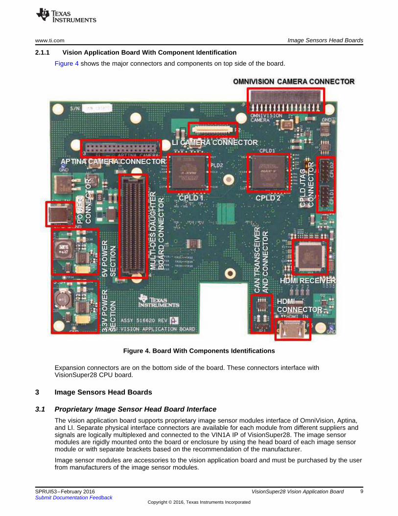
2.1.1 Vision Application Board With Component IdentificationFigure 4 shows the major connectors and components on top side of the board.
Figure 4. Board With Components Identifications
Expansion connectors are on the bottom side of the board. These connectors interface withVisionSuper28 CPU board.
3 Image Sensors Head Boards
3.1 Proprietary Image Sensor Head Board InterfaceThe vision application board supports proprietary image sensor modules interface of OmniVision, Aptina,and LI. Separate physical interface connectors are available for each module from different suppliers andsignals are logically multiplexed and connected to the VIN1A IP of VisionSuper28. The image sensormodules are rigidly mounted onto the board or enclosure by using the head board of each image sensormodule or with separate brackets based on the recommendation of the manufacturer.
Image sensor modules are accessories to the vision application board and must be purchased by the userfrom manufacturers of the image sensor modules.

Image Sensors Head Boards www.ti.com
10 SPRUI53–February 2016Submit Documentation Feedback
Copyright © 2016, Texas Instruments Incorporated
VisionSuper28 Vision Application Board
3.1.1 LI – Single Sensor Head BoardFigure 5 shows that this image sensor board must be connected to the vision application board throughflex cable assembly.
Figure 5. LI Image Sensor Head Board Assembly
The bracket for this image sensor head board is available from LI. Order this through the LI webpage.
3.1.2 LI – Dual Sensor Head BoardLI high-resolution dual image sensor board LI-M024-DUAL incorporates two Aptina 1.2M CMOS digitalimage sensors MT9M024. Dual image sensor board LI-M024-DUAL has an option to use either singleimage sensor board or dual image sensor board. If used as a dual image sensor board, J3 and J4connectors must be connected through FPC cable and the J1 connector must be connected to processorboard through a flex cable.
NOTE: The flex cable to connect J3 and J4 is supplied with the image sensor board. Their LI partnumber is LI-FLEX03. Purchase the cable to connect J1 to the processor board separately athttp://shop.leopardimaging.com/product.sc?productId=55. Ensure the length of the cable is6cm.
Compared to the single image sensor head board, dual image sensor head board does not require a SPIinterface and has an additional signal called Trigger on one of the NC pins of signal image sensor headboard. The trigger pin can be controlled through the allocated GPIO pin shown in Section 3.8.
NOTE: The LI dual image sensor board does not have a holding bracket, like the one available forsingle image sensor headboard. As Figure 6 shows, use a custom L-bracket for mounting ontop of a silver box and vision application board.

www.ti.com Image Sensors Head Boards
11SPRUI53–February 2016Submit Documentation Feedback
Copyright © 2016, Texas Instruments Incorporated
VisionSuper28 Vision Application Board
Figure 6. LI Dual Image Sensor Head Board Mounting
3.1.3 OmniVision Imager
3.1.3.1 Mounting DetailsThe Omnivision image sensor does not require a special assembly to mount on top of a PCB. The sensoris directly connected with VisionSuper28 through a board-to-board connector. For more information, seeFigure 7.
Figure 7. OmniVision Imager Head Board Assembly

Image Sensors Head Boards www.ti.com
12 SPRUI53–February 2016Submit Documentation Feedback
Copyright © 2016, Texas Instruments Incorporated
VisionSuper28 Vision Application Board
As Figure 8 shows, the OmniVision imager head board does require a holder to position on top of silverbox.
Figure 8. OmniVision Image Head Board Assembly on Silver Box
The holder part number is TFCCA-40-01 from Richo.
3.1.4 Aptina Imager – Head Board
3.1.4.1 Mechanical ArrangementsAn Aptina adapter card is used to provide mechanical support and easy way to electronically interface withthe vision application board. For more information, see Figure 9.
Figure 9. Aptina Head Board Assembly

www.ti.com Image Sensors Head Boards
13SPRUI53–February 2016Submit Documentation Feedback
Copyright © 2016, Texas Instruments Incorporated
VisionSuper28 Vision Application Board
3.2 FPD-Link III FMC DS90UB914Q Daughter Board InterfaceThe six-channel FPD-Link III daughterboard offers up to six high-speed forward channels and a full duplexback channel for data transmission over a single differential pair. Each channel uses a TI DS90UB914Qde-serializer with its DS90UB913Q counterpart (on the remote serializer board) to form a serializer andde-serializer pair. Due to the nature of the DS90UB914Q and DS90UB913Q pair, only one I2C bus isrequired to access and configure all I2C devices attached to the FPD-Link daughter board.
The vision application board supports the selection of up to six camera modules based on the use casesand requirements. Four camera modules are supported at the highest data bus width and five or sixcameras are supported using narrower data bus widths for each camera module.
Number of Cameras and Interface Configuration Option:• When five or six channels are used, the maximum supported number of data signals per channel is
eight or nine and horizontal sync (hsync), vertical sync (vsync), and clock.• When six channels are used without vsync, ten data lines plus hsync and clock can be handled.• When four channels are used, twelve data signals per channel and, hsync, vsync, and clock can be
handled.
This configuration selection process is performed on the FPD-Link III FMC DS90UB914Q multideserializerdaughter board. Based on the implemented configuration on this board, the demultiplexing must beperformed on the CPLD available from the vision application board to extract the appropriate requiredsignal per the configuration in the FPD-Link III board.
3.2.1 CAM Signal DemultiplexingDepending on the configurations of the number of channels, usage, and number of data lines, a fewsignals are multiplexed and transmitted from the serializer end. Those signal must be de-multiplexed inthe de-serializer end.
Table 2 shows which signals are multiplexed according to the configuration option in the FPD-Link IIIboard.
Table 2. List of De-Multiplexed Signals
FPD_A FPD_B FPD_CCAM6_D1_CAM3_VS CAM1_D0_CAM1_VS CAM5_D1_CAM1_VSCAM6_D2_CAM3_D10 CAM2_D0_CAM2_VS CAM5_D2_CAM1_D10CAM6_D3_CAM3_D11 CAM3_D0_CAM3_VS CAM5_D3_CAM1_D11CAM6_D4_CAM4_VS CAM4_D0_CAM4_VS CAM5_D4_CAM2_VSCAM6_D5_CAM4_D10 CAM5_D0_CAM5_VS CAM5_D5_CAM2_D10CAM6_D6_CAM4_D11 CAM6_D0_CAM6_VS CAM5_D6_CAM2_D11
Table 3 and Table 4 show the method in which signals are de-multiplexed according to the configuration inthe FPC-Link III board.
Table 3. CAM Input De-Multiplexer
Image Sensor InterfaceOption DeMUX_FPD_A DeMUX_FPD_B DeMUX_FPD_C
6 Channels (8Bit, HS, VS,PCLK) S0=1 S0=0 S0=1
6 Channels (10Bit, HS, PCLK) S0=1 S0=1 S0=14 Channels (12Bit, HS, VS,
PCLK) S0=0 S0=1 S0=0

Image Sensors Head Boards www.ti.com
14 SPRUI53–February 2016Submit Documentation Feedback
Copyright © 2016, Texas Instruments Incorporated
VisionSuper28 Vision Application Board
Table 4. De-Multiplexing as Per Required Configuration
Signal NameControl Signal
S0 = 1 S0 = 0DeMUX_FPD_A
CAM6_D1_CAM3_VS CAM6_D1 CAM3_VSCAM6_D2_CAM3_D10 CAM6_D2 CAM3_D10CAM6_D3_CAM3_D11 CAM6_D3 CAM3_D11CAM6_D4_CAM4_VS CAM6_D4 CAM4_VSCAM6_D5_CAM4_D10 CAM6_D5 CAM4_D10CAM6_D6_CAM4_D11 CAM6_D6 CAM4_D11
DeMUX_FPD_BCAM1_D0_CAM1_VS CAM1_D0 CAM1_VSCAM2_D0_CAM2_VS CAM2_D0 CAM2_VSCAM3_D0_CAM3_VS CAM3_D0 CAM3_VSCAM4_D0_CAM4_VS CAM4_D0 CAM4_VSCAM5_D0_CAM5_VS CAM5_D0 CAM5_VSCAM6_D0_CAM6_VS CAM6_D0 CAM6_VS
DeMUX_FPD_CCAM5_D1_CAM1_VS CAM5_D1 CAM1_VSCAM5_D2_CAM1_D10 CAM5_D2 CAM1_D10CAM5_D3_CAM1_D11 CAM5_D3 CAM1_D11CAM5_D4_CAM2_VS CAM5_D4 CAM2_VSCAM5_D5_CAM2_D10 CAM5_D5 CAM2_D10CAM5_D6_CAM2_D11 CAM5_D6 CAM2_D11
3.2.2 Board Presence DetectionIn Row D, pins 30 and 31 are used for board presence detection, as shown in Figure 10.
Figure 10. Board Presence Detection
3.2.3 I2C Slave Address ConfigurationTo avoid I2C slave address conflict with the board info EEPROM, the FPD-Link III FMC DS90UB914Qdaughter board has an option to configure a I2C slave address by using the FMC_GA1(D35) andFMC_GA0(C34) pins.
For I2C slave address configurations, both pull-up and pull-down options are provided for theFMC_GA1(D35) and FMC_GA0(C34) pins.10K Ω 1% Tol. resistors are already available on these lines inthe FPD-Link III board.
By default, both the FMC_GA1 (D35) and FMC_GA0 (C34) nets are pulled down to ground.

www.ti.com Image Sensors Head Boards
15SPRUI53–February 2016Submit Documentation Feedback
Copyright © 2016, Texas Instruments Incorporated
VisionSuper28 Vision Application Board
3.3 HDMI Receiver InterfaceThe HDMI receiver on the vision apps board can be used to receive stored images from an externalstorage medium, and have the images played back on an external display through the HDMI transmitteravailable on the CPU board or through a wireless display.
Figure 11. HDMI Wiring Connection
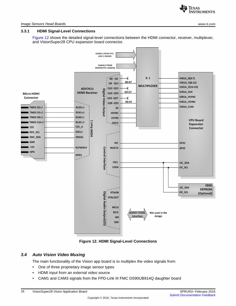
Image Sensors Head Boards www.ti.com
16 SPRUI53–February 2016Submit Documentation Feedback
Copyright © 2016, Texas Instruments Incorporated
VisionSuper28 Vision Application Board
3.3.1 HDMI Signal-Level ConnectionsFigure 12 shows the detailed signal-level connections between the HDMI connector, receiver, multiplexer,and VisionSuper28 CPU expansion board connector.
Figure 12. HDMI Signal-Level Connections
3.4 Auto Vision Video MuxingThe main functionality of the Vision app board is to multiplex the video signals from:• One of three proprietary image sensor types• HDMI input from an external video source• CAM1 and CAM3 signals from the FPD-Link III FMC DS90UB914Q daughter board
www.ti.com Image Sensors Head Boards
17SPRUI53–February 2016Submit Documentation Feedback
Copyright © 2016, Texas Instruments Incorporated
VisionSuper28 Vision Application Board
The Vision app board can be used as video muxing interface to run:• Captured running images from proprietary image sensors (or)• HDMI from an external video source interface (or)• Surround view or stereoscopic view from the FPD-Link III FMC DS90UB914Q daughter board
The Mux input selection chart is shown in Table 5.
Table 5. Mux Output Selection Chart
MUX2_SEL[1] MUX2_SEL[0] MUX_OUT0 0 HDMI RECEIVER
0 1
EXTERNAL IMAGERMUX1_SEL[1] MUX1_SEL[0] MUX_OUT
0 0 LI_IMAGER0 1 OV_IMAGER1 0 APTINA_IMAGER1 1 HIGH Z
1 0 CAM1 and CAM3 of FPD_LINK1 1 HIGH Z
Both a software and manual mode select are available. A dip switch is provided for the manual selection.For mapping, see Table 6.
Table 6. List of Dip Switch Signals
Position Description2-1 MUX1_SEL Manual Setting4-3 MUX2_SEL Manual Setting5 DeMux_FPD_A Manual Setting6 DeMux_FPD_B Manual Setting7 DeMux_FPD_C Manual Setting
8Mode Selection:0 – Use DIP SWITCH for configuration (manual control)1 – Use control signals for configuration (software control)
For the camera inputs (OmniVision, Aptina, Leopard Imaging), there are two different data modesavailable: straight data and shifted data, as shown in Table 7.
Table 7. Camera Data Modes
Camera InputControl Signal (DeMux_FPD_B)
=0 (Shift) =1 (Straight)OmniVision Data = “00” and (9 to 2) Data = (9 downto 0)
Aptina Data = “0000” and (11 to 4) Data = (11 downto 0)Leopard Imaging Data = “0000” and (13 to 4) Data = (13 downto 0)
3.5 CPLD LogicAll the required logic for CAM signal de-multiplexing (see Section 3.2.1), and CAM signal buffering andauto vision multiplexing (see Section 3.4) are implemented with CPLDs to ensure the propagation delay iswithin the limit. CPLD 5M2210ZF324C4M from Altera has been used for this logic implementation.Figure 13 shows the top-level blocks of logic implemented in the CPLDs. There are two numbers ofCPLDs used for this logic implementation.

Image Sensors Head Boards www.ti.com
18 SPRUI53–February 2016Submit Documentation Feedback
Copyright © 2016, Texas Instruments Incorporated
VisionSuper28 Vision Application Board
Figure 13. CPLD Logic Implementation

www.ti.com Image Sensors Head Boards
19SPRUI53–February 2016Submit Documentation Feedback
Copyright © 2016, Texas Instruments Incorporated
VisionSuper28 Vision Application Board
Table 8 shows the VIN signal mapping.
Table 8. VIN and Camera Signal Mapping
Signal Name Signal at Exp. Conn Signal Used AsCAM1_D[11:0] VIN1A_D[11:0] VIN1A_D[11:0]CAM1_HSYNC VIN1A_HSYNC VIN1A_HSYNCCAM1_VSYNC VIN1A_VSYNC VIN1A_VSYNCCAM1_PCLK VIN1A_CLK0 VIN1A_CLK0
CAM2_D[11:0] VIN2A[11:0] VIN2A[11:0]CAM2_HSYNC VIN2A_HSYNC VIN2A_HSYNCCAM2_VSYNC VIN2A_VSYNC VIN2A_VSYNCCAM2_PCLK VIN2A_CLK0 VIN2A_CLK0CAM3_D[0:7] VIN1A_D[16:23] VIN3A_[0:7]CAM3_D[8:11] VIN2A_D[16:19] VIN3A_[8:11]CAM3_HSYNC VIN2A_D[22] VIN3A_HSYNCCAM3_VSYNC VIN2A_D[23] VIN3A_VSYNCCAM3_PCLK VIN1B_CLK1 VIN3A_CLK0CAM4_D[0] VIN5A_D[0] MMC3_DAT[5]CAM4_D[1] VIN5A_D[1] MMC3_DAT[4]CAM4_D[2] VIN5A_D[2] MMC3_DAT[3]CAM4_D[3] VIN5A_D[3] MMC3_DAT[2]CAM4_D[4] VIN5A_D[4] MMC3_DAT[1]CAM4_D[5] VIN5A_D[5] MMC3_DAT[0]CAM4_D[6] VIN5A_D[6] MMC3_CMDCAM4_D[7] VIN5A_D[7] MMC3_CLK
CAM4_D[8:11] VIN5A_D[8:11] VIN5A_D[8:11]CAM4_HSYNC MMC3_DAT[6] VIN5A_HSYNC0CAM4_VSYNC MMC3_DAT[7] VIN5A_VSYNC0CAM4_PCLK VIN5A_CLK0 VIN5A_CLK0CAM5_D[2:9] VIN4B_D[0:7] VIN4B_D[0:7]
CAM5_HSYNC VIN4B_HSYNC1 VIN4B_HSYNC1CAM5_VSYNC VIN4B_VSYNC1 VIN4B_VSYNC1CAM5_PCLK VIN4B_CLK1 VIN4B_CLK1CAM6_D[0:3] VIN6A_D[0:3] VIN6A_D[0:3]CAM6_D[4] McASP2_AXR3 VIN6A_d[4]CAM6_D[5] McASP2_AXR2 VIN6A_d[5]CAM6_D[6] McASP2_AFSX VIN6A_d[6]
CAM6_D[7:9] VIN6A_D[7:9] VIN6A_D[7:9]CAM6_HSYNC VIN6A_HSYNC VIN6A_HSYNCCAM6_VSYNC VIN6A_VSYNC VIN6A_VSYNCCAM6_PCLK MCA6_AHCLKX VIN6A_CLK0
3.6 CAN InterfaceCAN PHY SN65HVDA541 is used in the DCAN2 interface of the VisionSuper28 CPU to provide supportfor the CAN interface in the Vision apps board.

Image Sensors Head Boards www.ti.com
20 SPRUI53–February 2016Submit Documentation Feedback
Copyright © 2016, Texas Instruments Incorporated
VisionSuper28 Vision Application Board
3.7 I2C InterfaceTable 9 shows the list of I2C slave devices in the Vision app board and Figure 14 shows the interface tothe master device (VisionSuper28 CPU) on I2C2.
(1) LSB Bit '0' :0 - Write access1 - Read access
Table 9. I2C Devices Slave Address
S. No Device (1) Slave Address (7-bit of MSB)1 LI Single Imager - LI-OV01633 0x0110 0002 LI Dual Imager -LI-M024-DUAL
a Image Sensor MT9M024-1 0x0010 000b Image Sensor MT9M024-2 0x0011 000
3 OV Imager - OV10635 0x0110 0004 Aptina Imager - AR0132 0x0010 0005 FBD-Link III FMC DS90UB914Q Daughter card
a GPIO Expander 1 (for configuration and control register ) 0x0100 111b GPIO Expander 2 (for configuration and control register ) 0x0100 110c GPIO Expander 3 (for configuration and control register ) 0x0100 101d INFO EEPROM 0x1010 000e De-Serializer 1 0x1100 000f De-Serializer 2 0x1100 100g De-Serializer 3 0x1101 000h De-Serializer 4 0x1101 100i De-Serializer 5 0x1100 001j De-Serializer 6 0x1101 001
6 HDMI Receiver – ADV7611a HDMI IO map 0x1001 100b CP map (disabled by default) 0x00 (Program)c HDMI map (disabled by default) 0x00 (Program)d Repeater map (disabled by default) 0x00 (Program)e EDID map (disabled by default) 0x00 (Program)f InfoFrame map (disabled by default) 0x00 (Program)g CEC map (disabled by default) 0x00 (Program)
7 Optional EEPROM 0x1010 000

www.ti.com Image Sensors Head Boards
21SPRUI53–February 2016Submit Documentation Feedback
Copyright © 2016, Texas Instruments Incorporated
VisionSuper28 Vision Application Board
Figure 14. I2C Interface in Vision Apps Board

Image Sensors Head Boards www.ti.com
22 SPRUI53–February 2016Submit Documentation Feedback
Copyright © 2016, Texas Instruments Incorporated
VisionSuper28 Vision Application Board
There is an optional EEPROM connected between the E-DDC and I2C2 bus, through the signal switch forHDMI handshaking when connected to the HDMI media devices. This signal switch is used to connect theI2C2 bus for writing, and the E-DDC bus for reading, by changing the signal switch inter-connections usingthe selected pin.
Figure 15. HDMI E-DDC I2C Interface
Table 10. HDMI E-DDC I2C Device Addresses
HDMI Receiver ADV7611 Device Slave Address (7-bit of MSB)E-DDC Bus Interface EDID (Programmable)Optional EEPROM 0x1010 000

www.ti.com Image Sensors Head Boards
23SPRUI53–February 2016Submit Documentation Feedback
Copyright © 2016, Texas Instruments Incorporated
VisionSuper28 Vision Application Board
3.8 GPIO Control and MonitorTable 11 shows the list of GPIOs required for monitor, control, and reset in Vision apps board devices andcomponents.
Table 11. GPIO Mapping of Device Control
Function Peripheral Device Vision Apps Bd NetVision Apps Bd Net
(I/F Conn Ref Des.Pin)GPIO/Sym
Ball Name (Ball No.)
Camera Aptina Imager APT_TRIGGER_VIN[5]A_D[12]
VIN[5]A_D[12] (EXP_P1.9) MCASP4_AXR1 (D17)
Camera OmniVision OV_PWDN GP6[17] (EXP_P1 .15) XREF_CLK0 (D18)GPIO6_17
Interface CAN PHY CAN_MODE_SEL_GPIO
VIN[5]A_D[13] (EXP_P1.18) MCASP4_AXR0 (G16)
Imager Imager/HDMI Receiver GPIO_USER_RESET VIN[5]A_D[15] (EXP_P1.12) MCASP4_ACLKX (C18)
HDMI Recorder HDMI Receiver HDMI_EVNODD MCA2_AXR1(EXP_P2.33) MCASP2_AXR1 (A15)
HDMI Recorder HDMI Receiver HDMI_INT GP5[1] (EXP_P2.36) MCASP1_FSR (J14)GPIO5_1
HDMI Recorder HDMI Receiver HDMI_SCDT GP5[0] (EXP_P2.34) MCASP1_ACLKR (B14)GPIO5_0
HDMI Recorder HDMI Receiver HDMI_CEC_D GP5[17] (EXP_P2.32) RMII_MHZ_50_CLK(U3) GPIO5_17
Remote camera I/F FPD_LINK III Brd FPD_LINK_DB_DET MCA2_AXR0(EXP_P2.37) MCASP2_AXR0 (B15)
Camera LI Dual Image Sensor LI_DUAL_Trigger VIN[5]A_D[14] (EXP_P1.11) MCASP4_FSX (A21)
CPLD control and statussignals
CPLD Logic DEMUX_FPD_B MCA2_AXR4(EXP_P2.23)
MCASP2_AXR4 (D15)GPIO1_4
CPLD Logic DEMUX_FPD_A MCA2_AXR6(EXP_P2.22)
MCASP2_AXR6 (B17)GPIO2_29
CPLD Logic DEMUX_FPD_C MCA2_AXR5(EXP_P2.24)
MCASP2_AXR5 (B16)GPIO6_7
CPLD Logic MUX1_SEL0 VIN2A_D[12](EXP_P2.93)
VIN2A_D12 (D5)GPIO4_13
CPLD Logic MUX2_SEL0 VIN[2]A_D[14](EXP_P2.95)
VIN2A_D14 (C3)GPIO4_15
CPLD Logic MUX1_SEL1 VIN2A_D[13](EXP_P2.94)
VIN2A_D13 (C2)GPIO4_14
CPLD Logic MUX1_SEL1 VIN2A_D[15](EXP_P2.96)
VIN2A_D15 (C4)GPIO4_16

Camera Module
Aptina
Camera Module
OmniVision
Camera Module
LI
CAN Transceiver
SN65HVDA541
CPLD 2
DS90UB914Q
Adapter Card
175mA
HDMI Transceiver
210mA
220mA
21mA
0.3mA
70mA
90mA
90mA
326mA
366mA
8mA
2300mA
400mA
CPLD 1
152mA
152mA
TPS74701
1.8V
TPS74701
1.2V
Input Power 44735mW @ 85% Efficiency
(12V @ 3727mA)
TPS74701
3.3V
TPS54362PWPRQ1
3.3V @ 1431mA
TPS54362PWPRQ1
5V @ 850mA
EN(3.3V from CPU
board)
Image Sensors Head Boards www.ti.com
24 SPRUI53–February 2016Submit Documentation Feedback
Copyright © 2016, Texas Instruments Incorporated
VisionSuper28 Vision Application Board
3.9 Power Supply TreeThe Vision apps board power supply tree is shown in Figure 16.
Figure 16. Power Supply Tree Chart

www.ti.com References
25SPRUI53–February 2016Submit Documentation Feedback
Copyright © 2016, Texas Instruments Incorporated
VisionSuper28 Vision Application Board
4 References• TDA2x EVM CPU Board User's Guide (SPRUI51)• TDA2x Vision EVM Application Board PCB Rev D (SPRR224)• TDA2x Vision EVM Application Board Schematic Rev D (SPRR225)• TDA2x Vision EVM Application Board CPLD Rev D (SPRR226)• TDA2x Vision EVM Application Board BOM Rev D (SPRR227)• TDA2x Vision EVM Application Board CPU Assembly Drawing Rev D (SPRR228)• TDA2x Vision EVM Application Board CPU PCB Drawing Rev D (SPRR229)

STANDARD TERMS AND CONDITIONS FOR EVALUATION MODULES1. Delivery: TI delivers TI evaluation boards, kits, or modules, including any accompanying demonstration software, components, or
documentation (collectively, an “EVM” or “EVMs”) to the User (“User”) in accordance with the terms and conditions set forth herein.Acceptance of the EVM is expressly subject to the following terms and conditions.1.1 EVMs are intended solely for product or software developers for use in a research and development setting to facilitate feasibility
evaluation, experimentation, or scientific analysis of TI semiconductors products. EVMs have no direct function and are notfinished products. EVMs shall not be directly or indirectly assembled as a part or subassembly in any finished product. Forclarification, any software or software tools provided with the EVM (“Software”) shall not be subject to the terms and conditionsset forth herein but rather shall be subject to the applicable terms and conditions that accompany such Software
1.2 EVMs are not intended for consumer or household use. EVMs may not be sold, sublicensed, leased, rented, loaned, assigned,or otherwise distributed for commercial purposes by Users, in whole or in part, or used in any finished product or productionsystem.
2 Limited Warranty and Related Remedies/Disclaimers:2.1 These terms and conditions do not apply to Software. The warranty, if any, for Software is covered in the applicable Software
License Agreement.2.2 TI warrants that the TI EVM will conform to TI's published specifications for ninety (90) days after the date TI delivers such EVM
to User. Notwithstanding the foregoing, TI shall not be liable for any defects that are caused by neglect, misuse or mistreatmentby an entity other than TI, including improper installation or testing, or for any EVMs that have been altered or modified in anyway by an entity other than TI. Moreover, TI shall not be liable for any defects that result from User's design, specifications orinstructions for such EVMs. Testing and other quality control techniques are used to the extent TI deems necessary or asmandated by government requirements. TI does not test all parameters of each EVM.
2.3 If any EVM fails to conform to the warranty set forth above, TI's sole liability shall be at its option to repair or replace such EVM,or credit User's account for such EVM. TI's liability under this warranty shall be limited to EVMs that are returned during thewarranty period to the address designated by TI and that are determined by TI not to conform to such warranty. If TI elects torepair or replace such EVM, TI shall have a reasonable time to repair such EVM or provide replacements. Repaired EVMs shallbe warranted for the remainder of the original warranty period. Replaced EVMs shall be warranted for a new full ninety (90) daywarranty period.
3 Regulatory Notices:3.1 United States
3.1.1 Notice applicable to EVMs not FCC-Approved:This kit is designed to allow product developers to evaluate electronic components, circuitry, or software associated with the kitto determine whether to incorporate such items in a finished product and software developers to write software applications foruse with the end product. This kit is not a finished product and when assembled may not be resold or otherwise marketed unlessall required FCC equipment authorizations are first obtained. Operation is subject to the condition that this product not causeharmful interference to licensed radio stations and that this product accept harmful interference. Unless the assembled kit isdesigned to operate under part 15, part 18 or part 95 of this chapter, the operator of the kit must operate under the authority ofan FCC license holder or must secure an experimental authorization under part 5 of this chapter.3.1.2 For EVMs annotated as FCC – FEDERAL COMMUNICATIONS COMMISSION Part 15 Compliant:
CAUTIONThis device complies with part 15 of the FCC Rules. Operation is subject to the following two conditions: (1) This device may notcause harmful interference, and (2) this device must accept any interference received, including interference that may causeundesired operation.Changes or modifications not expressly approved by the party responsible for compliance could void the user's authority tooperate the equipment.
FCC Interference Statement for Class A EVM devicesNOTE: This equipment has been tested and found to comply with the limits for a Class A digital device, pursuant to part 15 ofthe FCC Rules. These limits are designed to provide reasonable protection against harmful interference when the equipment isoperated in a commercial environment. This equipment generates, uses, and can radiate radio frequency energy and, if notinstalled and used in accordance with the instruction manual, may cause harmful interference to radio communications.Operation of this equipment in a residential area is likely to cause harmful interference in which case the user will be required tocorrect the interference at his own expense.
SPACER
SPACER
SPACER
SPACER
SPACER
SPACER
SPACER
SPACER

FCC Interference Statement for Class B EVM devicesNOTE: This equipment has been tested and found to comply with the limits for a Class B digital device, pursuant to part 15 ofthe FCC Rules. These limits are designed to provide reasonable protection against harmful interference in a residentialinstallation. This equipment generates, uses and can radiate radio frequency energy and, if not installed and used in accordancewith the instructions, may cause harmful interference to radio communications. However, there is no guarantee that interferencewill not occur in a particular installation. If this equipment does cause harmful interference to radio or television reception, whichcan be determined by turning the equipment off and on, the user is encouraged to try to correct the interference by one or moreof the following measures:
• Reorient or relocate the receiving antenna.• Increase the separation between the equipment and receiver.• Connect the equipment into an outlet on a circuit different from that to which the receiver is connected.• Consult the dealer or an experienced radio/TV technician for help.
3.2 Canada3.2.1 For EVMs issued with an Industry Canada Certificate of Conformance to RSS-210
Concerning EVMs Including Radio Transmitters:This device complies with Industry Canada license-exempt RSS standard(s). Operation is subject to the following two conditions:(1) this device may not cause interference, and (2) this device must accept any interference, including interference that maycause undesired operation of the device.
Concernant les EVMs avec appareils radio:Le présent appareil est conforme aux CNR d'Industrie Canada applicables aux appareils radio exempts de licence. L'exploitationest autorisée aux deux conditions suivantes: (1) l'appareil ne doit pas produire de brouillage, et (2) l'utilisateur de l'appareil doitaccepter tout brouillage radioélectrique subi, même si le brouillage est susceptible d'en compromettre le fonctionnement.
Concerning EVMs Including Detachable Antennas:Under Industry Canada regulations, this radio transmitter may only operate using an antenna of a type and maximum (or lesser)gain approved for the transmitter by Industry Canada. To reduce potential radio interference to other users, the antenna typeand its gain should be so chosen that the equivalent isotropically radiated power (e.i.r.p.) is not more than that necessary forsuccessful communication. This radio transmitter has been approved by Industry Canada to operate with the antenna typeslisted in the user guide with the maximum permissible gain and required antenna impedance for each antenna type indicated.Antenna types not included in this list, having a gain greater than the maximum gain indicated for that type, are strictly prohibitedfor use with this device.
Concernant les EVMs avec antennes détachablesConformément à la réglementation d'Industrie Canada, le présent émetteur radio peut fonctionner avec une antenne d'un type etd'un gain maximal (ou inférieur) approuvé pour l'émetteur par Industrie Canada. Dans le but de réduire les risques de brouillageradioélectrique à l'intention des autres utilisateurs, il faut choisir le type d'antenne et son gain de sorte que la puissance isotroperayonnée équivalente (p.i.r.e.) ne dépasse pas l'intensité nécessaire à l'établissement d'une communication satisfaisante. Leprésent émetteur radio a été approuvé par Industrie Canada pour fonctionner avec les types d'antenne énumérés dans lemanuel d’usage et ayant un gain admissible maximal et l'impédance requise pour chaque type d'antenne. Les types d'antennenon inclus dans cette liste, ou dont le gain est supérieur au gain maximal indiqué, sont strictement interdits pour l'exploitation del'émetteur
3.3 Japan3.3.1 Notice for EVMs delivered in Japan: Please see http://www.tij.co.jp/lsds/ti_ja/general/eStore/notice_01.page 日本国内に
輸入される評価用キット、ボードについては、次のところをご覧ください。http://www.tij.co.jp/lsds/ti_ja/general/eStore/notice_01.page
3.3.2 Notice for Users of EVMs Considered “Radio Frequency Products” in Japan: EVMs entering Japan may not be certifiedby TI as conforming to Technical Regulations of Radio Law of Japan.
If User uses EVMs in Japan, not certified to Technical Regulations of Radio Law of Japan, User is required by Radio Law ofJapan to follow the instructions below with respect to EVMs:1. Use EVMs in a shielded room or any other test facility as defined in the notification #173 issued by Ministry of Internal
Affairs and Communications on March 28, 2006, based on Sub-section 1.1 of Article 6 of the Ministry’s Rule forEnforcement of Radio Law of Japan,
2. Use EVMs only after User obtains the license of Test Radio Station as provided in Radio Law of Japan with respect toEVMs, or
3. Use of EVMs only after User obtains the Technical Regulations Conformity Certification as provided in Radio Law of Japanwith respect to EVMs. Also, do not transfer EVMs, unless User gives the same notice above to the transferee. Please notethat if User does not follow the instructions above, User will be subject to penalties of Radio Law of Japan.
SPACER
SPACER
SPACER
SPACER
SPACER

【無線電波を送信する製品の開発キットをお使いになる際の注意事項】 開発キットの中には技術基準適合証明を受けていないものがあります。 技術適合証明を受けていないもののご使用に際しては、電波法遵守のため、以下のいずれかの措置を取っていただく必要がありますのでご注意ください。1. 電波法施行規則第6条第1項第1号に基づく平成18年3月28日総務省告示第173号で定められた電波暗室等の試験設備でご使用
いただく。2. 実験局の免許を取得後ご使用いただく。3. 技術基準適合証明を取得後ご使用いただく。
なお、本製品は、上記の「ご使用にあたっての注意」を譲渡先、移転先に通知しない限り、譲渡、移転できないものとします。上記を遵守頂けない場合は、電波法の罰則が適用される可能性があることをご留意ください。 日本テキサス・イ
ンスツルメンツ株式会社東京都新宿区西新宿6丁目24番1号西新宿三井ビル
3.3.3 Notice for EVMs for Power Line Communication: Please see http://www.tij.co.jp/lsds/ti_ja/general/eStore/notice_02.page電力線搬送波通信についての開発キットをお使いになる際の注意事項については、次のところをご覧ください。http://www.tij.co.jp/lsds/ti_ja/general/eStore/notice_02.page
SPACER4 EVM Use Restrictions and Warnings:
4.1 EVMS ARE NOT FOR USE IN FUNCTIONAL SAFETY AND/OR SAFETY CRITICAL EVALUATIONS, INCLUDING BUT NOTLIMITED TO EVALUATIONS OF LIFE SUPPORT APPLICATIONS.
4.2 User must read and apply the user guide and other available documentation provided by TI regarding the EVM prior to handlingor using the EVM, including without limitation any warning or restriction notices. The notices contain important safety informationrelated to, for example, temperatures and voltages.
4.3 Safety-Related Warnings and Restrictions:4.3.1 User shall operate the EVM within TI’s recommended specifications and environmental considerations stated in the user
guide, other available documentation provided by TI, and any other applicable requirements and employ reasonable andcustomary safeguards. Exceeding the specified performance ratings and specifications (including but not limited to inputand output voltage, current, power, and environmental ranges) for the EVM may cause personal injury or death, orproperty damage. If there are questions concerning performance ratings and specifications, User should contact a TIfield representative prior to connecting interface electronics including input power and intended loads. Any loads appliedoutside of the specified output range may also result in unintended and/or inaccurate operation and/or possiblepermanent damage to the EVM and/or interface electronics. Please consult the EVM user guide prior to connecting anyload to the EVM output. If there is uncertainty as to the load specification, please contact a TI field representative.During normal operation, even with the inputs and outputs kept within the specified allowable ranges, some circuitcomponents may have elevated case temperatures. These components include but are not limited to linear regulators,switching transistors, pass transistors, current sense resistors, and heat sinks, which can be identified using theinformation in the associated documentation. When working with the EVM, please be aware that the EVM may becomevery warm.
4.3.2 EVMs are intended solely for use by technically qualified, professional electronics experts who are familiar with thedangers and application risks associated with handling electrical mechanical components, systems, and subsystems.User assumes all responsibility and liability for proper and safe handling and use of the EVM by User or its employees,affiliates, contractors or designees. User assumes all responsibility and liability to ensure that any interfaces (electronicand/or mechanical) between the EVM and any human body are designed with suitable isolation and means to safelylimit accessible leakage currents to minimize the risk of electrical shock hazard. User assumes all responsibility andliability for any improper or unsafe handling or use of the EVM by User or its employees, affiliates, contractors ordesignees.
4.4 User assumes all responsibility and liability to determine whether the EVM is subject to any applicable international, federal,state, or local laws and regulations related to User’s handling and use of the EVM and, if applicable, User assumes allresponsibility and liability for compliance in all respects with such laws and regulations. User assumes all responsibility andliability for proper disposal and recycling of the EVM consistent with all applicable international, federal, state, and localrequirements.
5. Accuracy of Information: To the extent TI provides information on the availability and function of EVMs, TI attempts to be as accurateas possible. However, TI does not warrant the accuracy of EVM descriptions, EVM availability or other information on its websites asaccurate, complete, reliable, current, or error-free.
SPACER
SPACER
SPACER
SPACER
SPACER
SPACER

SPACER6. Disclaimers:
6.1 EXCEPT AS SET FORTH ABOVE, EVMS AND ANY WRITTEN DESIGN MATERIALS PROVIDED WITH THE EVM (AND THEDESIGN OF THE EVM ITSELF) ARE PROVIDED "AS IS" AND "WITH ALL FAULTS." TI DISCLAIMS ALL OTHERWARRANTIES, EXPRESS OR IMPLIED, REGARDING SUCH ITEMS, INCLUDING BUT NOT LIMITED TO ANY IMPLIEDWARRANTIES OF MERCHANTABILITY OR FITNESS FOR A PARTICULAR PURPOSE OR NON-INFRINGEMENT OF ANYTHIRD PARTY PATENTS, COPYRIGHTS, TRADE SECRETS OR OTHER INTELLECTUAL PROPERTY RIGHTS.
6.2 EXCEPT FOR THE LIMITED RIGHT TO USE THE EVM SET FORTH HEREIN, NOTHING IN THESE TERMS ANDCONDITIONS SHALL BE CONSTRUED AS GRANTING OR CONFERRING ANY RIGHTS BY LICENSE, PATENT, OR ANYOTHER INDUSTRIAL OR INTELLECTUAL PROPERTY RIGHT OF TI, ITS SUPPLIERS/LICENSORS OR ANY OTHER THIRDPARTY, TO USE THE EVM IN ANY FINISHED END-USER OR READY-TO-USE FINAL PRODUCT, OR FOR ANYINVENTION, DISCOVERY OR IMPROVEMENT MADE, CONCEIVED OR ACQUIRED PRIOR TO OR AFTER DELIVERY OFTHE EVM.
7. USER'S INDEMNITY OBLIGATIONS AND REPRESENTATIONS. USER WILL DEFEND, INDEMNIFY AND HOLD TI, ITSLICENSORS AND THEIR REPRESENTATIVES HARMLESS FROM AND AGAINST ANY AND ALL CLAIMS, DAMAGES, LOSSES,EXPENSES, COSTS AND LIABILITIES (COLLECTIVELY, "CLAIMS") ARISING OUT OF OR IN CONNECTION WITH ANYHANDLING OR USE OF THE EVM THAT IS NOT IN ACCORDANCE WITH THESE TERMS AND CONDITIONS. THIS OBLIGATIONSHALL APPLY WHETHER CLAIMS ARISE UNDER STATUTE, REGULATION, OR THE LAW OF TORT, CONTRACT OR ANYOTHER LEGAL THEORY, AND EVEN IF THE EVM FAILS TO PERFORM AS DESCRIBED OR EXPECTED.
8. Limitations on Damages and Liability:8.1 General Limitations. IN NO EVENT SHALL TI BE LIABLE FOR ANY SPECIAL, COLLATERAL, INDIRECT, PUNITIVE,
INCIDENTAL, CONSEQUENTIAL, OR EXEMPLARY DAMAGES IN CONNECTION WITH OR ARISING OUT OF THESETERMS ANDCONDITIONS OR THE USE OF THE EVMS PROVIDED HEREUNDER, REGARDLESS OF WHETHER TI HASBEEN ADVISED OF THE POSSIBILITY OF SUCH DAMAGES. EXCLUDED DAMAGES INCLUDE, BUT ARE NOT LIMITEDTO, COST OF REMOVAL OR REINSTALLATION, ANCILLARY COSTS TO THE PROCUREMENT OF SUBSTITUTE GOODSOR SERVICES, RETESTING, OUTSIDE COMPUTER TIME, LABOR COSTS, LOSS OF GOODWILL, LOSS OF PROFITS,LOSS OF SAVINGS, LOSS OF USE, LOSS OF DATA, OR BUSINESS INTERRUPTION. NO CLAIM, SUIT OR ACTION SHALLBE BROUGHT AGAINST TI MORE THAN ONE YEAR AFTER THE RELATED CAUSE OF ACTION HAS OCCURRED.
8.2 Specific Limitations. IN NO EVENT SHALL TI'S AGGREGATE LIABILITY FROM ANY WARRANTY OR OTHER OBLIGATIONARISING OUT OF OR IN CONNECTION WITH THESE TERMS AND CONDITIONS, OR ANY USE OF ANY TI EVMPROVIDED HEREUNDER, EXCEED THE TOTAL AMOUNT PAID TO TI FOR THE PARTICULAR UNITS SOLD UNDERTHESE TERMS AND CONDITIONS WITH RESPECT TO WHICH LOSSES OR DAMAGES ARE CLAIMED. THE EXISTENCEOF MORE THAN ONE CLAIM AGAINST THE PARTICULAR UNITS SOLD TO USER UNDER THESE TERMS ANDCONDITIONS SHALL NOT ENLARGE OR EXTEND THIS LIMIT.
9. Return Policy. Except as otherwise provided, TI does not offer any refunds, returns, or exchanges. Furthermore, no return of EVM(s)will be accepted if the package has been opened and no return of the EVM(s) will be accepted if they are damaged or otherwise not ina resalable condition. If User feels it has been incorrectly charged for the EVM(s) it ordered or that delivery violates the applicableorder, User should contact TI. All refunds will be made in full within thirty (30) working days from the return of the components(s),excluding any postage or packaging costs.
10. Governing Law: These terms and conditions shall be governed by and interpreted in accordance with the laws of the State of Texas,without reference to conflict-of-laws principles. User agrees that non-exclusive jurisdiction for any dispute arising out of or relating tothese terms and conditions lies within courts located in the State of Texas and consents to venue in Dallas County, Texas.Notwithstanding the foregoing, any judgment may be enforced in any United States or foreign court, and TI may seek injunctive reliefin any United States or foreign court.
Mailing Address: Texas Instruments, Post Office Box 655303, Dallas, Texas 75265Copyright © 2015, Texas Instruments Incorporated
spacer

IMPORTANT NOTICE
Texas Instruments Incorporated and its subsidiaries (TI) reserve the right to make corrections, enhancements, improvements and otherchanges to its semiconductor products and services per JESD46, latest issue, and to discontinue any product or service per JESD48, latestissue. Buyers should obtain the latest relevant information before placing orders and should verify that such information is current andcomplete. All semiconductor products (also referred to herein as “components”) are sold subject to TI’s terms and conditions of salesupplied at the time of order acknowledgment.TI warrants performance of its components to the specifications applicable at the time of sale, in accordance with the warranty in TI’s termsand conditions of sale of semiconductor products. Testing and other quality control techniques are used to the extent TI deems necessaryto support this warranty. Except where mandated by applicable law, testing of all parameters of each component is not necessarilyperformed.TI assumes no liability for applications assistance or the design of Buyers’ products. Buyers are responsible for their products andapplications using TI components. To minimize the risks associated with Buyers’ products and applications, Buyers should provideadequate design and operating safeguards.TI does not warrant or represent that any license, either express or implied, is granted under any patent right, copyright, mask work right, orother intellectual property right relating to any combination, machine, or process in which TI components or services are used. Informationpublished by TI regarding third-party products or services does not constitute a license to use such products or services or a warranty orendorsement thereof. Use of such information may require a license from a third party under the patents or other intellectual property of thethird party, or a license from TI under the patents or other intellectual property of TI.Reproduction of significant portions of TI information in TI data books or data sheets is permissible only if reproduction is without alterationand is accompanied by all associated warranties, conditions, limitations, and notices. TI is not responsible or liable for such altereddocumentation. Information of third parties may be subject to additional restrictions.Resale of TI components or services with statements different from or beyond the parameters stated by TI for that component or servicevoids all express and any implied warranties for the associated TI component or service and is an unfair and deceptive business practice.TI is not responsible or liable for any such statements.Buyer acknowledges and agrees that it is solely responsible for compliance with all legal, regulatory and safety-related requirementsconcerning its products, and any use of TI components in its applications, notwithstanding any applications-related information or supportthat may be provided by TI. Buyer represents and agrees that it has all the necessary expertise to create and implement safeguards whichanticipate dangerous consequences of failures, monitor failures and their consequences, lessen the likelihood of failures that might causeharm and take appropriate remedial actions. Buyer will fully indemnify TI and its representatives against any damages arising out of the useof any TI components in safety-critical applications.In some cases, TI components may be promoted specifically to facilitate safety-related applications. With such components, TI’s goal is tohelp enable customers to design and create their own end-product solutions that meet applicable functional safety standards andrequirements. Nonetheless, such components are subject to these terms.No TI components are authorized for use in FDA Class III (or similar life-critical medical equipment) unless authorized officers of the partieshave executed a special agreement specifically governing such use.Only those TI components which TI has specifically designated as military grade or “enhanced plastic” are designed and intended for use inmilitary/aerospace applications or environments. Buyer acknowledges and agrees that any military or aerospace use of TI componentswhich have not been so designated is solely at the Buyer's risk, and that Buyer is solely responsible for compliance with all legal andregulatory requirements in connection with such use.TI has specifically designated certain components as meeting ISO/TS16949 requirements, mainly for automotive use. In any case of use ofnon-designated products, TI will not be responsible for any failure to meet ISO/TS16949.
Products ApplicationsAudio www.ti.com/audio Automotive and Transportation www.ti.com/automotiveAmplifiers amplifier.ti.com Communications and Telecom www.ti.com/communicationsData Converters dataconverter.ti.com Computers and Peripherals www.ti.com/computersDLP® Products www.dlp.com Consumer Electronics www.ti.com/consumer-appsDSP dsp.ti.com Energy and Lighting www.ti.com/energyClocks and Timers www.ti.com/clocks Industrial www.ti.com/industrialInterface interface.ti.com Medical www.ti.com/medicalLogic logic.ti.com Security www.ti.com/securityPower Mgmt power.ti.com Space, Avionics and Defense www.ti.com/space-avionics-defenseMicrocontrollers microcontroller.ti.com Video and Imaging www.ti.com/videoRFID www.ti-rfid.comOMAP Applications Processors www.ti.com/omap TI E2E Community e2e.ti.comWireless Connectivity www.ti.com/wirelessconnectivity
Mailing Address: Texas Instruments, Post Office Box 655303, Dallas, Texas 75265Copyright © 2016, Texas Instruments Incorporated