adc3xxx, adc3xjxx evm user’s guide - texas instruments · user's guide slau579c–june...
TRANSCRIPT

User's GuideSLAU579C–June 2014–Revised January 2016
ADC3xxx, ADC3xJxx EVM User’s Guide
This document is intended to serve as a user’s guide for the ADC3xxx EVM and ADC3xJxx EVM. TheEVMs provide a platform for evaluating the ADC3xxx which is a dual- or quad-channel, 12- or 14-bit serialLVDS interface, analog-to-digital converter (ADC) with sampling speed grades of 25, 50, 80, and 125Msps. The ADC3xJxx is a dual- or quad-channel, 12- or 14-bit JESD204B-compliant interface ADC withsampling speed grades of 50, 80, 125, and 160 Msps. This family of converters only requires a single 1.8-V supply, provides flexible input clock dividers, and provides internal features for improved 1/f (ADC32xx,ADC34xx) and SFDR performance. Throughout this document, the abbreviations EVM and ADC3xxxx,and the term evaluation module are synonymous with the ADC3xxx EVM and ADC3xJxx EVM, unlessotherwise noted.
Contents1 Introduction ................................................................................................................... 3
1.1 EVM Block Diagram ................................................................................................ 41.2 EVM Power Supply ................................................................................................. 61.3 EVM Connectors and Jumpers ................................................................................... 71.4 EVM ADC Input Circuit Configurations ......................................................................... 10
2 Software Control............................................................................................................ 122.1 Installation Instructions ........................................................................................... 122.2 Software Operation ............................................................................................... 12
3 Basic Test Procedure ...................................................................................................... 213.1 Test Block Diagram with ADC32xx and ADC34xx............................................................ 213.2 Test Set-up Connection .......................................................................................... 223.3 ADC32/34xx and TSW1400 Setup Guide...................................................................... 223.4 Test Block Diagram with ADC32Jxx and ADC34Jxx ......................................................... 243.5 Test Set-up Connection (Onboard LMK04828 Clock)........................................................ 253.6 ADC32J/34Jxx and TSW14J56 Setup Guide.................................................................. 26
List of Figures
1 Simplified ADC344x EVM Block Diagram ................................................................................ 42 Simplified ADC34J4x EVM Block Diagram ............................................................................... 53 Simplified EVM Power Supply ............................................................................................. 64 ADC34Jxx EVM Connector and Jumper Locations ..................................................................... 75 ADC34xx EVM Connector and Jumper Locations ...................................................................... 86 ADC3xxxx ADC Input Circuit options .................................................................................... 117 DC34xx Clock Input Circuit ............................................................................................... 118 Common Tab ............................................................................................................... 139 ADC32xx Tab ............................................................................................................... 1410 ADC34XX Tab .............................................................................................................. 1611 ADC32Jxx Tab.............................................................................................................. 1812 ADC34Jxx Tab.............................................................................................................. 2013 ADC32xx/ADC34xx and TSW1400 Test Setup Block Diagram...................................................... 2114 Select ADC32xx or 34xx in the HSDC Pro GUI Program............................................................. 2215 ADC3xxx Operating in 14-Bit Mode at 125 Msps with 10-MHz Input Signal ....................................... 2316 ADC32Jxx/ADC34Jxx and TSW14J56 Test Setup Block Diagram.................................................. 24
All trademarks are the property of their respective owners.
1SLAU579C–June 2014–Revised January 2016 ADC3xxx, ADC3xJxx EVM User’s GuideSubmit Documentation Feedback
Copyright © 2014–2016, Texas Instruments Incorporated
www.ti.com
17 Select ADC32Jxx or 34Jxx in the HSDC Pro GUI Program .......................................................... 2618 ADC32Jxx Operating in 14-Bit Mode at 160 Msps with 10-MHz Input Signal ..................................... 27
List of Tables
1 ADC3xxx Family of Parts and EVMs...................................................................................... 32 Power Supply Options ...................................................................................................... 73 ADC3xxxx EVM Connectors ............................................................................................... 94 ADC3xxxx EVM Jumper Options......................................................................................... 105 ADC3xxxx EVM LED Indicators .......................................................................................... 10
2 ADC3xxx, ADC3xJxx EVM User’s Guide SLAU579C–June 2014–Revised January 2016Submit Documentation Feedback
Copyright © 2014–2016, Texas Instruments Incorporated

www.ti.com Introduction
1 IntroductionThe family of parts and 32 associated EVMs are categorized in Table 1.
Table 1. ADC3xxx Family of Parts and EVMs
ADC Device Interface Number of Number Max Msps EVMchannels of bits
ADC3221 sLVDS Dual 12 25 ADC3221EVMADC3222 12 50 ADC3222EVMADC3223 12 80 ADC3223EVMADC3224 12 125 ADC3224EVMADC3241 14 25 ADC3241EVMADC3242 14 50 ADC3242EVMADC3243 14 80 ADC3243EVMADC3244 14 125 ADC3244EVMADC3421 sLVDS Quad 12 25 ADC3421EVMADC3422 12 50 ADC3422EVMADC3423 12 80 ADC3423EVMADC3424 12 125 ADC3424EVMADC3441 14 25 ADC3441EVMADC3442 14 50 ADC3442EVMADC3443 14 80 ADC3443EVMADC3444 14 125 ADC3444EVMADC32J22 JESD204B Dual 12 50 ADC32J22EVMADC32J23 12 80 ADC32J23EVMADC32J24 12 125 ADC32J24EVMADC32J25 12 160 ADC32J25EVMADC32J42 14 50 ADC32J42EVMADC32J43 14 80 ADC32J43EVMADC32J44 14 125 ADC32J44EVMADC32J45 14 160 ADC32J45EVMADC34J22 JESD204B Quad 12 50 ADC34J22EVMADC34J23 12 80 ADC34J23EVMADC34J24 12 125 ADC34J24EVMADC34J25 12 160 ADC34J25EVMADC34J42 14 50 ADC34J42EVMADC34J43 14 80 ADC34J43EVMADC34J44 14 125 ADC34J44EVMADC34J45 14 160 ADC34J45EVM
There are 3 package sizes and pinouts for all of these parts. The sLVDS dual devices use a 7 × 7 mm,48-pin QFN, the sLVDS quad devices use an 8 × 8 mm, 56-pin QFN, and the dual and quad JESD204Bdevice share the same package using a 7 × 7 mm 48-pin QFN.
The Dual ADCs comprise 2 buffered inputs, 2 ADC cores, and a common input clock circuit. The quadADCs comprise 4 buffered inputs, 4 ADC cores and a common input clock circuit. The sLVDS versionshave a 2-wire interface per ADC (2 pairs of p/n signals) – for the dual this means 2 sets of 2-wireinterfaces (4 p/n pairs), the quad would have 4 sets of 2-wire interfaces (8 p/n pairs). Each of these 2 wireinterfaces can be operated in 1-wire mode (14x serialization) or 2-wire mode (7x serialization). For the 12bit devices this equates to 12x and 6x serialization. The JESD204B versions have 1 lane per ADC core.For the dual this means there will be 2 lanes per device and 4 lanes per device for the quad. Please referto the data sheet for more information on sLVDS serialization and JESD204B lane configurations.
3SLAU579C–June 2014–Revised January 2016 ADC3xxx, ADC3xJxx EVM User’s GuideSubmit Documentation Feedback
Copyright © 2014–2016, Texas Instruments Incorporated

CLK IN
14bit ADC
14bit ADC
14bit ADC
14bit ADC
Digital Block
+Output
Formatter
DCLK
DAB P/M sLVDS2
DCD P/M sLVDS2
Power SupplyCircuits
USBToSPI
5VUSB
ADC34xx
CH A
CH B
CH C
CH D
FCLK
Introduction www.ti.com
1.1 EVM Block DiagramFigure 1 and Figure 2 show a simplified block diagram of the default configuration of the EVM. The two orfour analog inputs are supplied to the EVM through a single-ended SMA connection, then transformercoupled to turn the single ended signal into a balanced differential signal and then input to the ADC32xxxor ADC34xxx. A dual transformer input circuit is used for better phase and amplitude balance of the inputsignal than would typically be produced by a single transformer input circuit.
Figure 1. Simplified ADC344x EVM Block Diagram
4 ADC3xxx, ADC3xJxx EVM User’s Guide SLAU579C–June 2014–Revised January 2016Submit Documentation Feedback
Copyright © 2014–2016, Texas Instruments Incorporated

14bit ADC
14bit ADC
14bit ADC
14bit ADC
Digital Block
+Output
Formatter
SYNC
SERDES Lane 0,12
SERDES Lane 3,42
Power SupplyCircuits
USBToSPI
5VUSB
ADC34Jxx
CLK IN
CH A
CH B
CH C
CH D
SYSREF
LMK04828
www.ti.com Introduction
Figure 2. Simplified ADC34J4x EVM Block Diagram
The clock input is supplied by way of a single-ended signal to an SMA connector and transformer coupledto produce a differential clock signal for the ADC32/34xx EVM. For the ADC32J/34Jxx EVM the clockinput can be generated on board using the LMK04828.
Power to the ADC3xxx EVM is typically supplied from a 5V bench supply via the onboard barrel connectorand the provided cable, or from an appropriate 5-V, 3A minimum power brick. All necessary voltages forthe ADC EVM are derived from the 5-V input connection.
5SLAU579C–June 2014–Revised January 2016 ADC3xxx, ADC3xJxx EVM User’s GuideSubmit Documentation Feedback
Copyright © 2014–2016, Texas Instruments Incorporated

GND
5VTPS62080
1
TPS7A4700 1.8V To ADC
4V to Amp
PWR IN
TPS2400
1
TPS7A4700
Overvoltage Protection Circuit
DC/DC Converter
Low Noise LDO
Low Noise LDO
ADC32/34xx EVM
GND
5VTPS62080
1
TPS7A4700 1.8V To ADC
4V to Amp
PWR IN
TPS2400
1
TPS7A4700
Overvoltage Protection Circuit
DC/DC Converter
Low Noise LDO
Low Noise LDO
ADC32J/34Jxx EVM
TPS62080
1
TPS7A4700 3.3V to LMK04828
1
Low Noise LDO
Introduction www.ti.com
1.2 EVM Power SupplyFigure 3 illustrates the power supply options available on the ADC3xxx EVM. Jumpers are used to choosethe power supply options, with the default jumper positions indicated by the darker portion of the jumperthat represents the presence of the jumper. Refer to Table 2 for jumper and feedback resistorconfiguration.
Figure 3. Simplified EVM Power Supply
6 ADC3xxx, ADC3xJxx EVM User’s Guide SLAU579C–June 2014–Revised January 2016Submit Documentation Feedback
Copyright © 2014–2016, Texas Instruments Incorporated
www.ti.com Introduction
Table 2. Power Supply Options
Device DescriptionADC32xx Default connection for LDO 1.8-V supply, switch both to 2-3 to use the switcher U4, install R79 for 1.8-VJP6: 1-2, JP7: 1-2 switcher outputADC34xx Default connection for LDO 1.8-V supply, switch both to 2-3 to use the switcher U4, install R79 for 1.8-VJP6: 1-2, JP7: 1-2 switcher outputADC342J/34Jxx spacerJP9: 1-2, JP10: 1-2 Default connection for LDO 1.8-V supply, switch both to 2-3 to use the switcher U8, install R152 for 1.8-Vspacer switcher outputspacer spacerJP12: 1-2, JP13: 1-2 Default Connection for LDO 3.3 V for LMK04828 power and onboard SPI/CPLD, switch both to 2-3 to use
U11 switcher output, install R163 for 3.3-V switcher output
The default power path has an efficient dual output DC-DC switching power supply to first step down theinput supplies from 5 V to 4 V and 2.8 V for the subsequent low noise LDOs. The 4 V is used by an LDOto derive 3.3 V for the LMK04828 clock circuits on the ADC3xJxx EVMs. The 2.8 V is used by an LDO toderive a 1.8-V supply for the ADC and USB circuits.
The low noise LDOs can be bypassed to allow the DC/DC power supply to directly provide the ADCpower. Please note that the feedback resistors of the DC/DC converter need to be adjusted accordingly.Refer to the ADC EVM schematic for details.
1.3 EVM Connectors and JumpersFigure 4 and Figure 5 show the locations of the connectors, jumpers, pushbutton switches, and LED.
Figure 4. ADC34Jxx EVM Connector and Jumper Locations
7SLAU579C–June 2014–Revised January 2016 ADC3xxx, ADC3xJxx EVM User’s GuideSubmit Documentation Feedback
Copyright © 2014–2016, Texas Instruments Incorporated

Introduction www.ti.com
Figure 5. ADC34xx EVM Connector and Jumper Locations
The EVM has a barrel connector for 5-V power. The SMA connectors connect the ADC input and ADCclock input to the ADC. Typically, the ADC inputs are transformer-coupled to accept single-endedconnections. The input circuit can be configured to connect to two SMA connectors for differentialsignaling, if desired. Table 3 lists the connector information for the ADC3xxxx.
8 ADC3xxx, ADC3xJxx EVM User’s Guide SLAU579C–June 2014–Revised January 2016Submit Documentation Feedback
Copyright © 2014–2016, Texas Instruments Incorporated

www.ti.com Introduction
Table 3. ADC3xxxx EVM Connectors
Device Connector DescriptionADC32xx J1 AINP – positive input for A, Ch1 single ended input
J2 AINM – negative input for A, DNIJ3 BINM – negative input for B, DNIJ4 BINP – positive input for B, Ch2 single ended inputJ9 CLK_INP – positive CLK input, single ended clock inputJ10 CLK_INM – negative CLK input, DNIJ11 SYSREF_INP – positive input for SYSREF frame clock, single ended inputJ12 SYSREF_INM – negative SYSREF input, DNIJ13A, B HSMC data connector to TSW1400 evaluation platformJ14 Mini USB connector for SPI controlJ15 Power connector for 5-V adapter
ADC34xx J1 AINP – positive input for A, Ch1 single ended inputJ2 AINM – negative input for A, DNIJ3 BINM – negative input for B, DNIJ4 BINP – positive input for B, Ch2 single ended inputJ5 CINP – positive input for C, Ch3 single ended inputJ6 CINM – negative input for C, DNIJ7 DINM – negative input for D, DNIJ8 DINP – positive input for D, Ch4 single ended inputJ9 CLK_INP – positive CLK input, single ended clock inputJ10 CLK_INM – negative CLK input, DNIJ11 SYSREF_INP – positive input for SYSREF frame clock, single ended inputJ12 SYSREF_INM – negative SYSREF input, DNIJ13A, B HSMC data connector to TSW1400 evaluation platformJ14 Mini USB connector for SPI controlJ15 Power connector for 5-V adapter
ADC32J/34Jxx J1 AIN_CH-AP – positive input for CHA, single ended input (DNI for ADC32Jxx)J2 AIN_CH-AM – negative input, (DNI for ADC32Jxx)J3 BIN_CH-BP – positive input for CHB (CHA input for ADC32Jxx), single ended inputJ4 BIN_CH-BM – negative input for CHB (CHA input for ADC32Jxx)J5 CIN_CH-CP – positive input for CHC (CHB input for ADC32Jxx), single ended inputJ6 CIN_CH-CM – negative input for CHC (CHB input for ADC32Jxx)J7 DIN_CH-DP – positive input for CHD, single ended input (DNI for ADC32Jxx)J8 DIN_CH-DM – negative input, (DNI for ADC32Jxx)J9 EXT_ADC_CLK – external ADC clock connection for ADC, if neededJ23 EXT SYSREF+ - external SYSREF connection for ADC, if needed (positive input)J24 EXT SYSREF– - external SYSREF connection for ADC, if needed (negative input)J10 LMK_CLKIN – external input clock for LMK use, if needed (for clock distribution mode)J13 DCLKOUT6P – LMK output test point, positiveJ14 DCLKOUT6N – LMK output test point, negativeJ15 DCLKOUT7P – LMK output test point, positiveJ16 DCLKOUT7N – LMK output test point, positiveJ20 5-V input power jackJ18 Mini USB connector for SPI GUI controlJ19 CPLD JTAG port
9SLAU579C–June 2014–Revised January 2016 ADC3xxx, ADC3xJxx EVM User’s GuideSubmit Documentation Feedback
Copyright © 2014–2016, Texas Instruments Incorporated
Introduction www.ti.com
The on-board jumper options allow configuration of on-board power supplies and ADC options. Many ofthe jumper selections that involve DC inputs or static control signals are by way of push-on square postjumpers. The jumper options are listed in Table 4. Table 4 indicates the default settings of the jumpers asthe EVM is normally shipped.
Table 4. ADC3xxxx EVM Jumper Options
Device Jumper DescriptionADC32xx/ADC34xx JP1 3 pin Jumper – 2-3 Default connection, 1-2 to enable PwDn function
JP2, J3, JP4,JP5 2 pin Jumper - SPI access points, if needed – default should be installed
ADC32J/34Jxx JP1 3 pin Jumper – 2-3 Default connection, 1-2 to enable PwDn functionJP2, J3, JP4,JP5 2 pin Jumper - SPI access points, if needed – default should be installedJP6 2 pin, default is connected for powering onboard VCXOSJP1 3 pin, DNI, optional for VCXO that require enable on pin 2JP11 2 pin, normally connected to enable current monitor for 1.8-V supply to ADCJP8 3 pin, default 2-3 for USB SPI selection through CPLD, 1-2 used for FMC
connector based SPI port
There is a pushbutton on the ADC3xxxx EVM – SW1. Upon powering up, the ADC can either accepthardware reset by pressing SW1 or toggling the software reset switch on the ADC3xxxx EVM GUI. Thedefault reset configuration of the ADC is given in its respective data sheet.
LED D1 on the ADC32/34xxx is lit to show the presence of the 5-V supply voltage to the EVM. On theADC32J/34Jxx EVMs, LED D8 is used to show the presence of the 5-V supply voltage to the EVM.Table 5 lists the description of each LED indicator.
Table 5. ADC3xxxx EVM LED Indicators
Device LED DescriptionADC32xx/ADC34xx D1 5-V power indicator
ADC32J/34Jxx D1, D2 Status LED from CLKin SEL0/1 on LMKD3, D4 Status LED used to indicate LMK Lock or PLL LockD5 Status LED for JESD SYNCD6, D7 Spare LED indicators for FMC connectorD8 5-V power indicator
1.4 EVM ADC Input Circuit ConfigurationsFigure 6 shows the ADC3xxxx ADC input circuit. The default setup has a dual 1:1 impedance ratiotransformer input circuit to achieve better phase and amplitude balance of the input signal than wouldtypically be produced by a single transformer input circuit.
The default input termination is 50 Ω, which is formed by two 25-Ω resistors connected to the ADC VCMnode. By default the input circuit is set for operation within the 1st 2 Nyquist zones. For higher frequencyinputs use the high frequency input circuit as shown in Figure 6.
10 ADC3xxx, ADC3xJxx EVM User’s Guide SLAU579C–June 2014–Revised January 2016Submit Documentation Feedback
Copyright © 2014–2016, Texas Instruments Incorporated

CLK IN1:4
0.1PF
0.1PF
���:
���:
0.1PF
14bit ADC
Jp
Jn
39nH
39nH
��:
��:
��:
��:0.1PF 0.1PF 0.1PF
0.1PF
15:
15:
��:
��:
10pF10pF
1:1 1:1
VCM
0:
0:
0.1PF
0.1PF
14bit ADC
Jp
Jn
�:
�:
��:
��:0.1PF 0.1PF 0.1PF
0.1PF
�:
�:
��:
��:
56nH10pF
1:1 1:1
VCM
10:
10:
0.1PF
0.1PF
Default ± Low Input Frequency
High Input Frequency
www.ti.com Introduction
Figure 6. ADC3xxxx ADC Input Circuit options
Figure 7 shows the ADC3xxxx clock input circuit. The clock signal will go through 1:4 impedance ratiotransformer to increase the clock amplitude by two (that is, 1:4 impedance ratio equals to 1:2 voltageratio). The two 100-Ω resistors will impedance transform back to the primary side as 50-Ω load impedancefor the signal source generator. For ADC evaluation, set the signal generator output to approximately+10 dBm.
Figure 7. DC34xx Clock Input Circuit
11SLAU579C–June 2014–Revised January 2016 ADC3xxx, ADC3xJxx EVM User’s GuideSubmit Documentation Feedback
Copyright © 2014–2016, Texas Instruments Incorporated
Software Control www.ti.com
2 Software Control
2.1 Installation Instructions
1. Open the folder named ADC3xxxx_Installer_vxpx (xpx represents the latest version)2. Run Setup.exe3. Follow the on-screen instructions4. Once installed, launch by clicking on the ADC3xxxx_GUI_vxpx program in Start → All Programs →
Texas Instruments ADCs5. When plugging in the USB cable for the first time, you are prompted by the Found-New-Hardware-
Wizard to install the USB drivers.(a) When a pop-up screen opens, select Continue Downloading.(b) Follow the on-screen instructions to install the USB drivers(c) If needed, access the drivers directly in the install directory
2.2 Software OperationThe software allows programming control of the ADC3xxxx device. The front panel provides a tab for fullprogramming of the register map of the ADC3xxxx and an advanced tab that allows for custom registeraccesses. The GUI tabs provide a convenient and simplified interface to the most used registers of eachdevice.
12 ADC3xxx, ADC3xJxx EVM User’s Guide SLAU579C–June 2014–Revised January 2016Submit Documentation Feedback
Copyright © 2014–2016, Texas Instruments Incorporated
www.ti.com Software Control
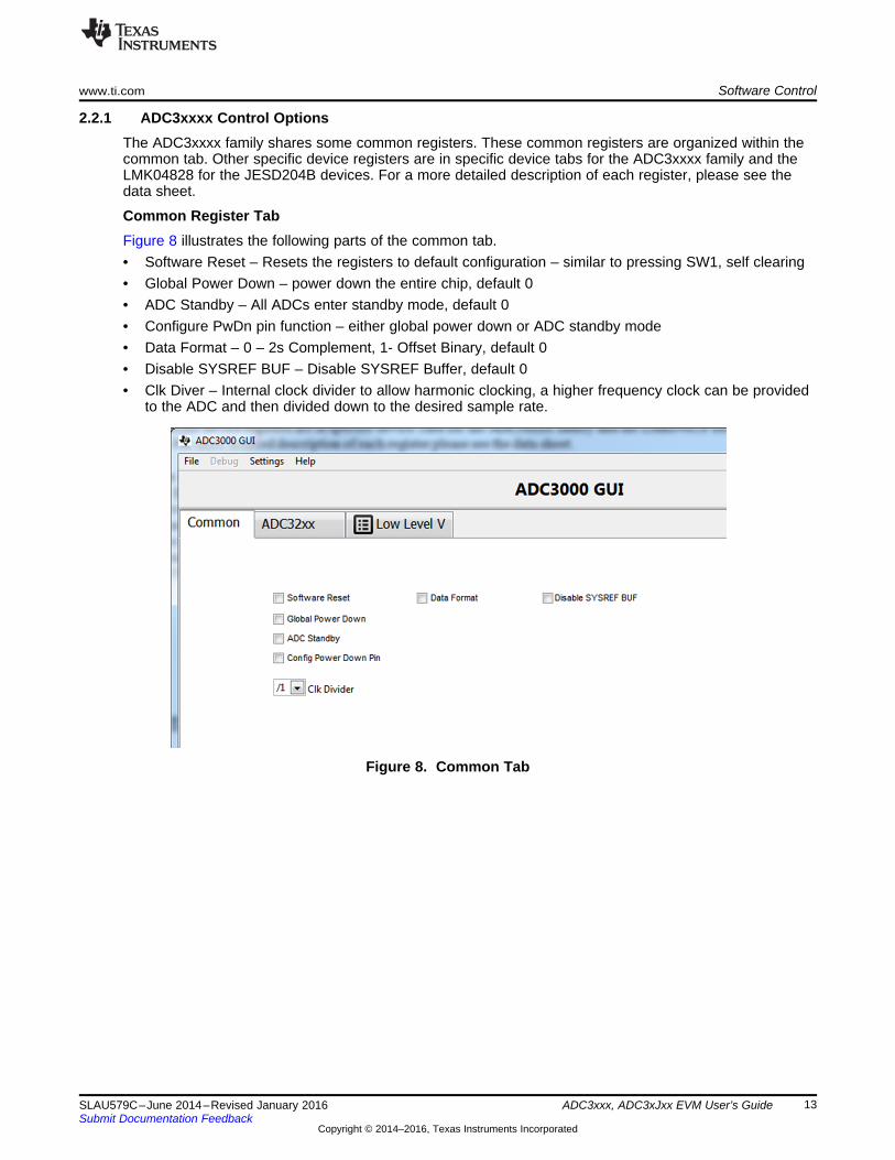
2.2.1 ADC3xxxx Control OptionsThe ADC3xxxx family shares some common registers. These common registers are organized within thecommon tab. Other specific device registers are in specific device tabs for the ADC3xxxx family and theLMK04828 for the JESD204B devices. For a more detailed description of each register, please see thedata sheet.
Common Register TabFigure 8 illustrates the following parts of the common tab.• Software Reset – Resets the registers to default configuration – similar to pressing SW1, self clearing• Global Power Down – power down the entire chip, default 0• ADC Standby – All ADCs enter standby mode, default 0• Configure PwDn pin function – either global power down or ADC standby mode• Data Format – 0 – 2s Complement, 1- Offset Binary, default 0• Disable SYSREF BUF – Disable SYSREF Buffer, default 0• Clk Diver – Internal clock divider to allow harmonic clocking, a higher frequency clock can be provided
to the ADC and then divided down to the desired sample rate.
Figure 8. Common Tab
13SLAU579C–June 2014–Revised January 2016 ADC3xxx, ADC3xJxx EVM User’s GuideSubmit Documentation Feedback
Copyright © 2014–2016, Texas Instruments Incorporated
Software Control www.ti.com
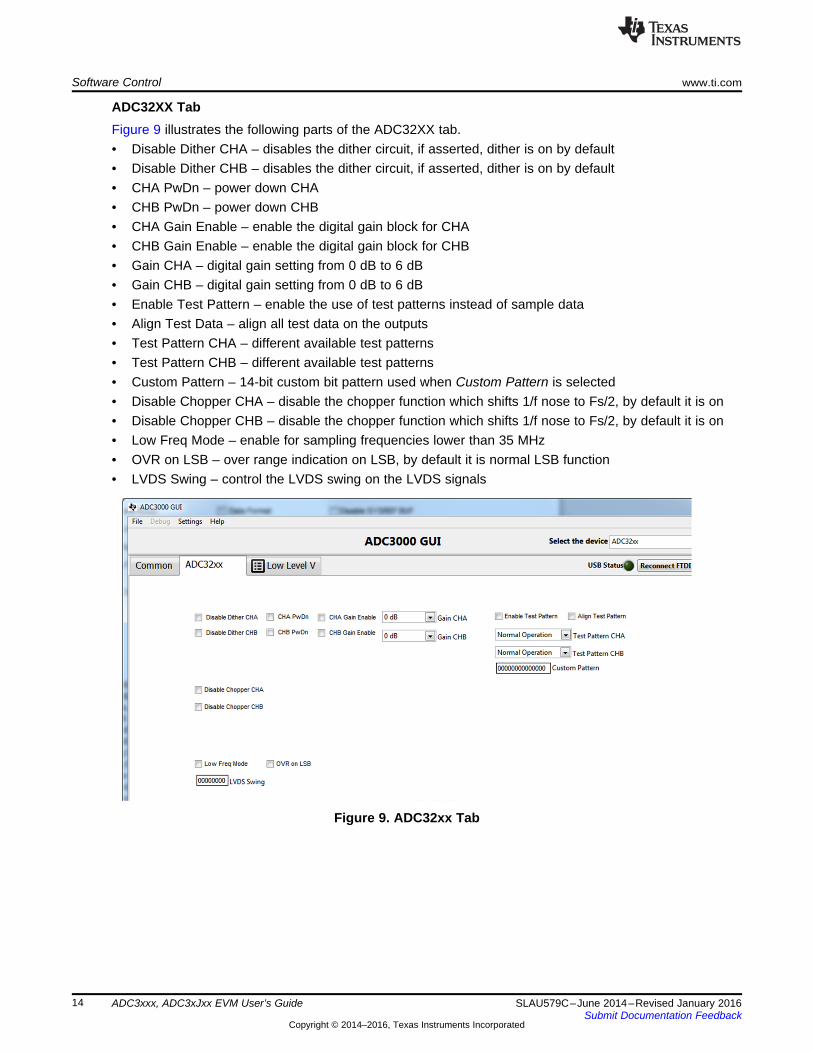
ADC32XX TabFigure 9 illustrates the following parts of the ADC32XX tab.• Disable Dither CHA – disables the dither circuit, if asserted, dither is on by default• Disable Dither CHB – disables the dither circuit, if asserted, dither is on by default• CHA PwDn – power down CHA• CHB PwDn – power down CHB• CHA Gain Enable – enable the digital gain block for CHA• CHB Gain Enable – enable the digital gain block for CHB• Gain CHA – digital gain setting from 0 dB to 6 dB• Gain CHB – digital gain setting from 0 dB to 6 dB• Enable Test Pattern – enable the use of test patterns instead of sample data• Align Test Data – align all test data on the outputs• Test Pattern CHA – different available test patterns• Test Pattern CHB – different available test patterns• Custom Pattern – 14-bit custom bit pattern used when Custom Pattern is selected• Disable Chopper CHA – disable the chopper function which shifts 1/f nose to Fs/2, by default it is on• Disable Chopper CHB – disable the chopper function which shifts 1/f nose to Fs/2, by default it is on• Low Freq Mode – enable for sampling frequencies lower than 35 MHz• OVR on LSB – over range indication on LSB, by default it is normal LSB function• LVDS Swing – control the LVDS swing on the LVDS signals
Figure 9. ADC32xx Tab
14 ADC3xxx, ADC3xJxx EVM User’s Guide SLAU579C–June 2014–Revised January 2016Submit Documentation Feedback
Copyright © 2014–2016, Texas Instruments Incorporated

www.ti.com Software Control
ADC34XX Tab• Disable Dither CHA – disables the dither circuit, if asserted, dither is on by default• Disable Dither CHB – disables the dither circuit, if asserted, dither is on by default• Disable Dither CHC – disables the dither circuit, if asserted, dither is on by default• Disable Dither CHD – disables the dither circuit, if asserted, dither is on by default• CHA PwDn – power down CHA• CHB PwDn – power down CHB• CHC PwDn – power down CHC• CHD PwDn – power down CHD• CHA Gain Enable – enable the digital gain block for CHA• CHB Gain Enable – enable the digital gain block for CHB• CHC Gain Enable – enable the digital gain block for CHC• CHD Gain Enable – enable the digital gain block for CHD• Gain CHA – digital gain setting from 0 dB to 6 dB• Gain CHB – digital gain setting from 0 dB to 6 dB• Gain CHC – digital gain setting from 0 dB to 6 dB• Gain CHD – digital gain setting from 0 dB to 6 dB• Enable Test Pattern – enable the use of test patterns instead of sample data• Align Test Data – align all test data on the outputs• Test Pattern CHA – different available test patterns• Test Pattern CHB – different available test patterns• Test Pattern CHC – different available test patterns• Test Pattern CHD – different available test patterns• Custom Pattern – 14-bit custom bit pattern used when Custom Pattern is selected• Disable Chopper CHA – disable the chopper function which shifts 1/f nose to Fs/2, default is on• Disable Chopper CHB – disable the chopper function which shifts 1/f nose to Fs/2, default is on• Disable Chopper CHC – disable the chopper function which shifts 1/f nose to Fs/2, default is on• Disable Chopper CHD – disable the chopper function which shifts 1/f nose to Fs/2, default is on• Low Freq Mode – enable for sampling frequencies lower than 35 MHz• OVR on LSB – over range indication on LSB, by default it is normal LSB function• LVDS Swing – control the LVDS swing on the LVDS signals
15SLAU579C–June 2014–Revised January 2016 ADC3xxx, ADC3xJxx EVM User’s GuideSubmit Documentation Feedback
Copyright © 2014–2016, Texas Instruments Incorporated

Software Control www.ti.com
Figure 10. ADC34XX Tab
16 ADC3xxx, ADC3xJxx EVM User’s Guide SLAU579C–June 2014–Revised January 2016Submit Documentation Feedback
Copyright © 2014–2016, Texas Instruments Incorporated
www.ti.com Software Control
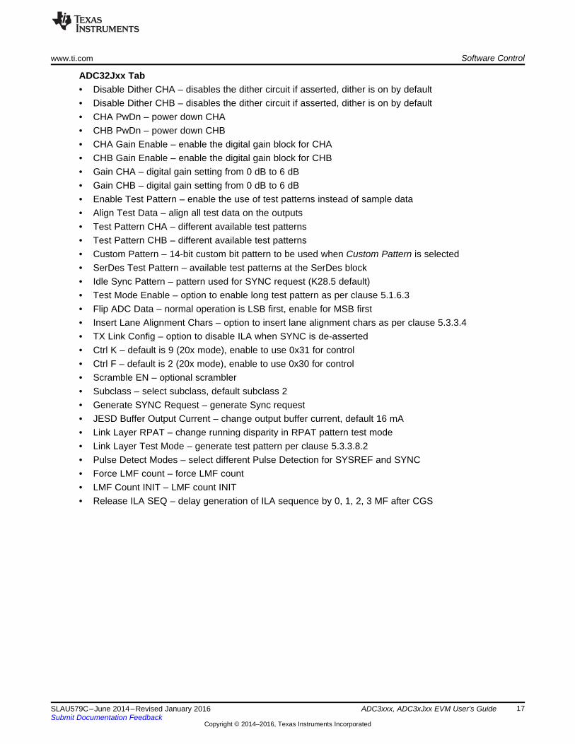
ADC32Jxx Tab• Disable Dither CHA – disables the dither circuit if asserted, dither is on by default• Disable Dither CHB – disables the dither circuit if asserted, dither is on by default• CHA PwDn – power down CHA• CHB PwDn – power down CHB• CHA Gain Enable – enable the digital gain block for CHA• CHB Gain Enable – enable the digital gain block for CHB• Gain CHA – digital gain setting from 0 dB to 6 dB• Gain CHB – digital gain setting from 0 dB to 6 dB• Enable Test Pattern – enable the use of test patterns instead of sample data• Align Test Data – align all test data on the outputs• Test Pattern CHA – different available test patterns• Test Pattern CHB – different available test patterns• Custom Pattern – 14-bit custom bit pattern to be used when Custom Pattern is selected• SerDes Test Pattern – available test patterns at the SerDes block• Idle Sync Pattern – pattern used for SYNC request (K28.5 default)• Test Mode Enable – option to enable long test pattern as per clause 5.1.6.3• Flip ADC Data – normal operation is LSB first, enable for MSB first• Insert Lane Alignment Chars – option to insert lane alignment chars as per clause 5.3.3.4• TX Link Config – option to disable ILA when SYNC is de-asserted• Ctrl K – default is 9 (20x mode), enable to use 0x31 for control• Ctrl F – default is 2 (20x mode), enable to use 0x30 for control• Scramble EN – optional scrambler• Subclass – select subclass, default subclass 2• Generate SYNC Request – generate Sync request• JESD Buffer Output Current – change output buffer current, default 16 mA• Link Layer RPAT – change running disparity in RPAT pattern test mode• Link Layer Test Mode – generate test pattern per clause 5.3.3.8.2• Pulse Detect Modes – select different Pulse Detection for SYSREF and SYNC• Force LMF count – force LMF count• LMF Count INIT – LMF count INIT• Release ILA SEQ – delay generation of ILA sequence by 0, 1, 2, 3 MF after CGS
17SLAU579C–June 2014–Revised January 2016 ADC3xxx, ADC3xJxx EVM User’s GuideSubmit Documentation Feedback
Copyright © 2014–2016, Texas Instruments Incorporated
Software Control www.ti.com
Figure 11. ADC32Jxx Tab
18 ADC3xxx, ADC3xJxx EVM User’s Guide SLAU579C–June 2014–Revised January 2016Submit Documentation Feedback
Copyright © 2014–2016, Texas Instruments Incorporated

www.ti.com Software Control
ADC34JXX Tab• Disable Dither CHA – disables the dither circuit if asserted, dither is on by default• Disable Dither CHB – disables the dither circuit if asserted, dither is on by default• Disable Dither CHC – disables the dither circuit if asserted, dither is on by default• Disable Dither CHD – disables the dither circuit if asserted, dither is on by default• CHA PwDn – power down CHA• CHB PwDn – power down CHB• CHC PwDn – power down CHC• CHD PwDn – power down CHD• CHA Gain Enable – enable the digital gain block for CHA• CHB Gain Enable – enable the digital gain block for CHB• CHC Gain Enable – enable the digital gain block for CHC• CHD Gain Enable – enable the digital gain block for CHD• Gain CHA – digital gain setting from 0 dB to 6 dB• Gain CHB – digital gain setting from 0 dB to 6 dB• Gain CHC – digital gain setting from 0 dB to 6 dB• Gain CHD – digital gain setting from 0 dB to 6 dB• Enable Test Pattern – enable the use of test patterns instead of sample data• Align Test Data – align all test data on the outputs• Test Pattern CHA – different available test patterns• Test Pattern CHB – different available test patterns• Test Pattern CHC – different available test patterns• Test Pattern CHD – different available test patterns• Custom Pattern – 14-bit custom bit pattern to be used when Custom Pattern is selected• SerDes Test Pattern – available test patterns at the SerDes block• Idle Sync Pattern – pattern used for SYNC request (K28.5 default)• Test Mode Enable – option to enable long test pattern as per clause 5.1.6.3• Flip ADC Data – normal operation is LSB first, enable for MSB first• Insert Lane Alignment Chars – option to insert lane alignment chars as per clause 5.3.3.4• TX Link Config – option to disable ILA when SYNC is de-asserted• Ctrl K – default is 9 (20x mode), enable to use 0x31 for control• Ctrl F – default is 2 (20x mode), enable to use 0x30 for control• Scramble EN – optional scrambler• Subclass – select subclass, default subclass 2• Generate SYNC Request – generate Sync request• JESD Buffer Output Current – change output buffer current, default 16 mA• Link Layer RPAT – change running disparity in RPAT pattern test mode• Link Layer Test Mode – generate test pattern per clause 5.3.3.8.2• Pulse Detect Modes – select different pulse detection for SYSREF and SYNC• Force LMF count – force LMF count• LMF Count INIT – LMF count INIT• Release ILA SEQ – delay generation of ILA sequence by 0, 1, 2, 3 MF after CGS
19SLAU579C–June 2014–Revised January 2016 ADC3xxx, ADC3xJxx EVM User’s GuideSubmit Documentation Feedback
Copyright © 2014–2016, Texas Instruments Incorporated

Software Control www.ti.com
Figure 12. ADC34Jxx Tab
LMK04828The registers for the LMK04828 are best described in the LMK04828 data sheet – they are not covered inthis users guide.
2.2.2 Low Level Register Control• Send All: Sends the register configuration to all devices• Read All: Reads register configuration from ADS58H40 device (not implemented in revision 1.x)• Save Regs: Saves the register configuration for all devices• Load Regs: Load a register file for all devices. Sample configuration files for common frequency plans
are located in the install directory.– Select the Load Regs button– Double click on the data folder– Double click on the desired register file– Click on Send All to ensure all the values are loaded properly
2.2.3 Misc Settings
• Reconnect FTDI: Toggle this button if the USB port is not responding. This generates a new USBhandle addressNOTE: Reset the board after every power cycle and then click the reconnect FTDI button on the GUI.
• File→Exit: Stops the program
20 ADC3xxx, ADC3xJxx EVM User’s Guide SLAU579C–June 2014–Revised January 2016Submit Documentation Feedback
Copyright © 2014–2016, Texas Instruments Incorporated

PC
USB
J15J5
USB Mini-B
Signal Generator(Input Source)
SignalGenerator
(CLK Source)
CLKJ9CHB
J4
CHAJ1
+5V
J5
J12
TSW1400
J3
CHCJ5
CHDJ8
+5VTo A, B, C, D
Channels
BPF BPF
SynchronizedSources
www.ti.com Basic Test Procedure
3 Basic Test ProcedureThis section outlines the basic test procedure for testing the EVM. There are 2 test platforms which can beused: (1) TSW1400 with ADC32xx and ADC34xx and (2) TSW14J56 or TSW14J50 with ADC32Jxx andADC34Jxx.
3.1 Test Block Diagram with ADC32xx and ADC34xxFigure 13 shows the test set-up for evaluation of the ADC3xxxx EVM with the TSW1400 Capture Card. Asseen in this figure, the evaluation setup involves a clock from a high-quality signal generator and a sinewave for the analog input from a high-quality signal generator. High order, narrow bandpass filters areusually required on clock and input frequencies to remove phase noise and harmonic content from theinput sine waves. If the two signal generators are not synchronized by an external reference signal tomake the clock and input frequency coherent, then the resulting fast Fourier transform (FFT) will first needto have a windowing function such as Blackman-Harris/Hamming/Hanning applied to the data.
Figure 13. ADC32xx/ADC34xx and TSW1400 Test Setup Block Diagram
21SLAU579C–June 2014–Revised January 2016 ADC3xxx, ADC3xJxx EVM User’s GuideSubmit Documentation Feedback
Copyright © 2014–2016, Texas Instruments Incorporated

Basic Test Procedure www.ti.com
3.2 Test Set-up Connection
1. Connect the ADC32xx/ADC34xx EVM J13 connector to the TSW1400 EVM J3 connector2. Connect 5 V to the TSW1400 J12 supply input connector and 5 V to the ADC32xx/34xx EVM J15
supply input connector3. Provide a sample clock at the ADC32xx/34xx EVM J9 SMA connector4. Provide a sine wave for the ADC32xx EVM J1 or J4 analog input and J1, J4, J5, or J8 of the ADC34xx
EVM5. Connect a USB cable from the TSW1400 to the programming computer6. For basic testing, the USB/SPI connection is not needed on the ADC32/34xx. Press SW1 to perform a
hardware reset. This will work with the default settings.7. Verify the following jumper connections on the ADC32/34xx EVM:
• JP1 – 2,3 default condition PDN is low• JP2, JP3, JP4, JP5 – Closed – default condition for SPI connection• JP6 – 1,2 default condition to select LDO power supply• JP7 – 1,2 default condition to select LDO power supply
3.3 ADC32/34xx and TSW1400 Setup GuidePlease reference the TSW1400 User’s Guide for more detailed explanations of the TSW1400 set-up andoperation. This document assumes the High-Speed Data Converter (HSDC) Pro software and theTSW1400 hardware are installed and functioning properly. The ADC32/34xx EVM requires High-SpeedData Converter Pro software version 2.6 or higher with TSW1400 hardware of Rev D (or higher).
Single tone FFT test1. Start the HSDC Pro GUI program. When the program starts, select the ADC tab and then select
ADC324x_2W_14bit.ini or ADC344x_2W_14bit.ini device in the Select ADC drop down menu.
Figure 14. Select ADC32xx or 34xx in the HSDC Pro GUI Program
2. When prompted with Load ADC Firmware?, select YES3. Select Single Tone FFT Test under Test Selection4. Select number of sample points (and resulting number of FFT bins) to be used. The example shown in
Figure 15 has 65536 samples.5. Enter the ADC32/34xx Sampling rate. The example shown in Figure 15 has the sample rate set at 125
Msps (filtered clock input around 10 dBm).6. Enter the input frequency desired. If the clock and input frequency signal generators are synchronized,
then make sure the checkbox for coherent frequency is checked and set the input frequency signalgenerator to the input frequency displayed. The example shown in Figure 15 has the input frequencyset at 10MHz (9.98878479MHx if coherent). Filtered signal input around 10 dBm – adjust to achieve –1dBFs on the HSDC Pro FFT.
7. Select channel 1, 2, 3, or 4 depending on the channel to which the signal generator is connected8. Press the Capture button on the HSDC Pro GUI
22 ADC3xxx, ADC3xJxx EVM User’s Guide SLAU579C–June 2014–Revised January 2016Submit Documentation Feedback
Copyright © 2014–2016, Texas Instruments Incorporated

www.ti.com Basic Test Procedure
9. Observe an FFT result similar to that of Figure 15
Figure 15. ADC3xxx Operating in 14-Bit Mode at 125 Msps with 10-MHz Input Signal
If the basic capture at this point is correct, then the front panel options of the SPI GUI and the front paneloptions of the TSW1400 GUI may be varied as desired to test out different device options.
23SLAU579C–June 2014–Revised January 2016 ADC3xxx, ADC3xJxx EVM User’s GuideSubmit Documentation Feedback
Copyright © 2014–2016, Texas Instruments Incorporated
PC
USB
USB J20J17
USB Mini-B
Signal Generator(Input Source)
LMK04828CHB
J3
CHAJ1
+5VJ11
TSW14J56
J4
USB Mini-B
CHCJ5
CHDJ7
+5VTo A, B, C, D
Channels
BPF
Basic Test Procedure www.ti.com
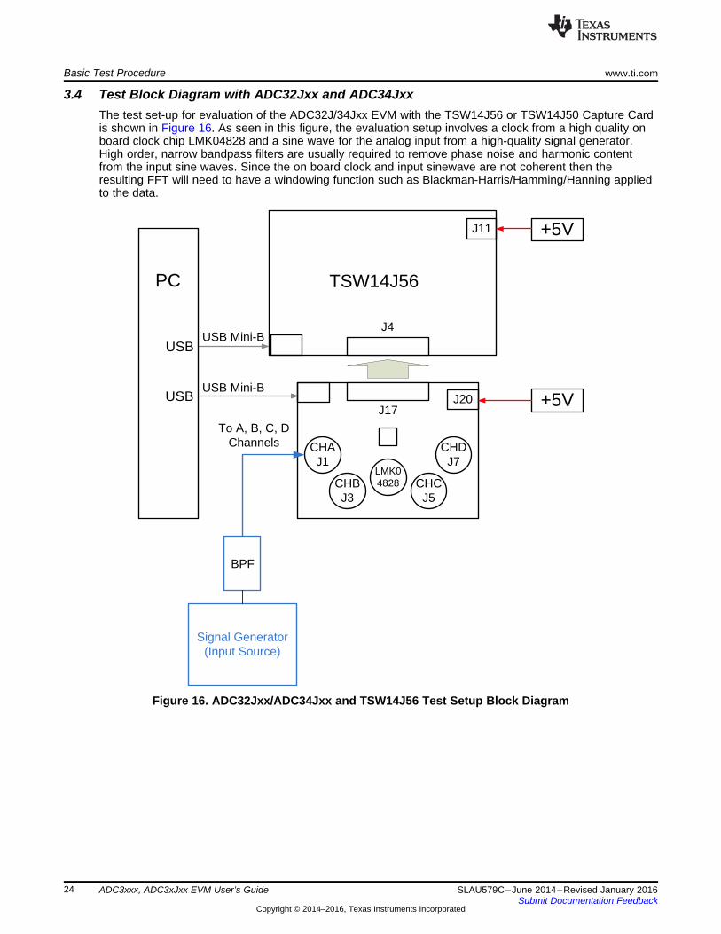
3.4 Test Block Diagram with ADC32Jxx and ADC34JxxThe test set-up for evaluation of the ADC32J/34Jxx EVM with the TSW14J56 or TSW14J50 Capture Cardis shown in Figure 16. As seen in this figure, the evaluation setup involves a clock from a high quality onboard clock chip LMK04828 and a sine wave for the analog input from a high-quality signal generator.High order, narrow bandpass filters are usually required to remove phase noise and harmonic contentfrom the input sine waves. Since the on board clock and input sinewave are not coherent then theresulting FFT will need to have a windowing function such as Blackman-Harris/Hamming/Hanning appliedto the data.
Figure 16. ADC32Jxx/ADC34Jxx and TSW14J56 Test Setup Block Diagram
24 ADC3xxx, ADC3xJxx EVM User’s Guide SLAU579C–June 2014–Revised January 2016Submit Documentation Feedback
Copyright © 2014–2016, Texas Instruments Incorporated

www.ti.com Basic Test Procedure
3.5 Test Set-up Connection (Onboard LMK04828 Clock)
1. Connect J17 connector of ADC32Jxx/ADC34Jxx EVM to J4 connector of TSW14J56 EVM (orTSW14J50 if desired)
2. Connect 5V to the J11 supply input connector of the TSW14J56 and 5V to the J20 supply inputconnector of the ADC32Jxx/34Jxx EVM
3. Connect a USB cable from the ADC32J/34Jxx EVM to the PC for SPI programming. TheADC32J/34Jxx EVMs require some programming for the on board clock requirements of theJESD204B interface.
4. Provide a sine wave for the analog input at J3 or J6 of ADC32Jxx EVM and J1, J3, J5, or J7 of theADC34Jxx EVM.
5. Connect USB cable from the TSW14J56 to the programming computer6. Verify the following jumper connections on the ADC32J/34Jxx EVM
• JP1 – 1,2 default condition PDN is low• JP2, JP3, JP4, JP5 – closed – default condition for SPI connection• JP6 – Closed – power for the onboard clock• JP8 – 2,3 – default condition to select USB port for SPI communication• JP9 – 1,2 – default condition select LDO power• JP10 – 1,2 – default condition select LDO power• JP12 – 1,2 – default condition select LDO power• JP13 – 1,2 – default condition select LDO power
25SLAU579C–June 2014–Revised January 2016 ADC3xxx, ADC3xJxx EVM User’s GuideSubmit Documentation Feedback
Copyright © 2014–2016, Texas Instruments Incorporated

Basic Test Procedure www.ti.com
3.6 ADC32J/34Jxx and TSW14J56 Setup GuidePlease reference the TSW14J56 User’s Guide for more detailed explanations of the TSW14J56 set-upand operation. This document assumes the HSDC Pro software and the TSW14J56 hardware areinstalled and functioning properly. The ADC32/34xx EVM requires HSDC Pro software version 2.6 orhigher with TSW14J56 hardware of Rev D (or higher).
Single Tone FFT Test1. The evaluation of the ADC32J/34Jxx EVM requires programming the LMK04828 clock source with the
correct PLL settings to provide a 160 Msps clock.• Connect a USB cable from the ADC32J/34Jxx EVM to the PC• Open the ADC3000 GUI, and connect to the ADC32Jxx or ADC34Jxx EVM• Go to the Low Level tab and click Load Config• Browse and find the ADC3xJxx_160MSPS_Operation_LMK_Setting.cfg• Check that the PLL2 LED D4 is lit – this indicates that the PLL is programmed properly and the
correct clocks are being generated2. Start the HSDC Pro GUI program. When the program starts, select the ADC tab and then select
ADC32Jxx_LMF_222 or ADC34Jxx_LMF_442 device in the Select ADC drop-down menu.
Figure 17. Select ADC32Jxx or 34Jxx in the HSDC Pro GUI Program
3. When prompted by Load ADC Firmware?, select YES4. Select Single Tone FFT Test under Test Selection5. Select the number of sample points (and resulting number of FFT bins) to be used. The example
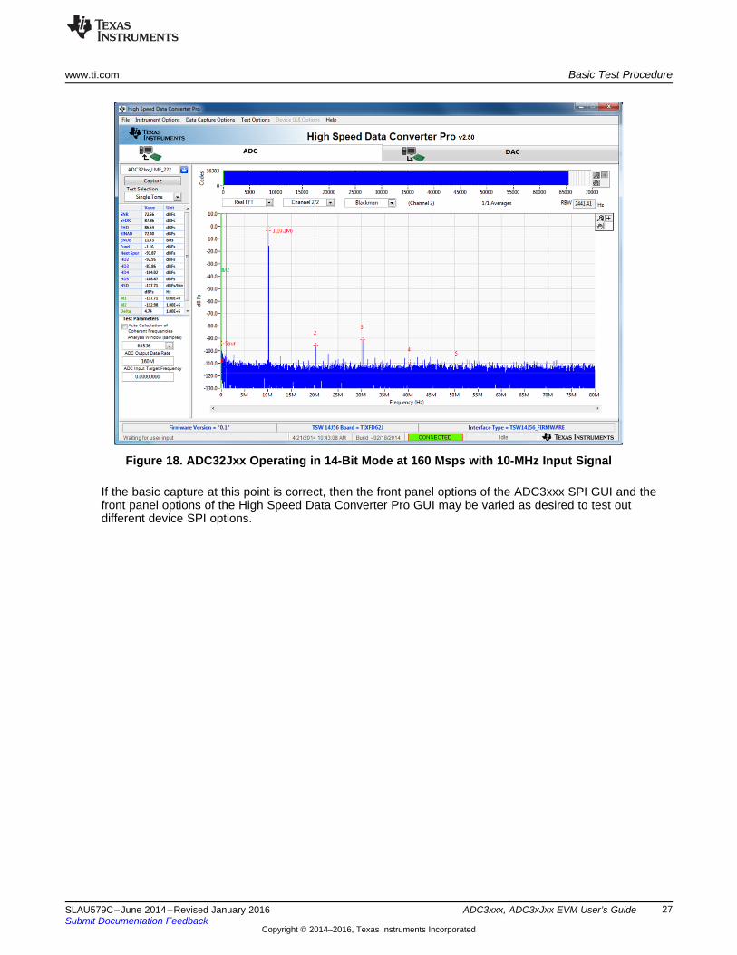
shown in Figure 18 has 65536 samples.6. Enter the ADC32J/34Jxx sampling rate. The example shown in Figure 16 has the sample rate set at
160 Msps7. Enter the input frequency desired. The example shown in Figure 16Figure 18 has the filtered input
frequency set at 10 MHz and around 10 dBm – adjust to achieve –1 dBFs on the HSDC Pro FFT plot8. Select channel 1, 2, 3, 4 depending on the channel to which the signal generator is connected9. Press the Capture button on the HSDC Pro GUI10. Observe an FFT result similar to that of Figure 16
26 ADC3xxx, ADC3xJxx EVM User’s Guide SLAU579C–June 2014–Revised January 2016Submit Documentation Feedback
Copyright © 2014–2016, Texas Instruments Incorporated
www.ti.com Basic Test Procedure
Figure 18. ADC32Jxx Operating in 14-Bit Mode at 160 Msps with 10-MHz Input Signal
If the basic capture at this point is correct, then the front panel options of the ADC3xxx SPI GUI and thefront panel options of the High Speed Data Converter Pro GUI may be varied as desired to test outdifferent device SPI options.
27SLAU579C–June 2014–Revised January 2016 ADC3xxx, ADC3xJxx EVM User’s GuideSubmit Documentation Feedback
Copyright © 2014–2016, Texas Instruments Incorporated

Revision History www.ti.com
Revision History
Changes from B Revision (January 2016) to C Revision ............................................................................................... Page
• Deleted references to future EVM releases from the ADC3xxx Family of Parts and EVMs table. ............................. 3• Added reference to TSW14J50 in the Basic Test Procedure section............................................................. 21• Added reference to TSW14J50 in the Test Block Diagram with ADC32Jxx and ADC34Jxx section. ........................ 24• Added reference to TSW14J50 in the Test Set-up Connection (Onboard LMK04828 Clock) section........................ 25
NOTE: Page numbers for previous revisions may differ from page numbers in the current version.
Revision History
Changes from A Revision (September 2014) to B Revision .......................................................................................... Page
• Changed the power supply reference to include options for using a 5-V brick or the provided power supply cable withbarrel connector. .......................................................................................................................... 5
Revision History
Changes from Original (June 2014) to A Revision ......................................................................................................... Page
• Deleted future release note from ADC3224EVM, ADC3424EVM, ADC34J25EVM, and ADC34J44EVM in Table 1........ 3• Added ADC32J22EVM, ADC32J42EVM, ADC34J22EVM, ADC34J42EVM to ADC3xxx Family of Parts and EVMs
table. ........................................................................................................................................ 3• Deleted last sentence in paragraph following Power Supply Options table. ...................................................... 7• Deleted last sentence in the first paragraph on the page........................................................................... 10• Deleted entire paragraph preceding ADC3xxxx EVM Jumper Options table. ................................................... 10• Deleted several rows from ADC3xxxx EVM Jumper Options table. .............................................................. 10
28 Revision History SLAU579C–June 2014–Revised January 2016Submit Documentation Feedback
Copyright © 2014–2016, Texas Instruments Incorporated
STANDARD TERMS AND CONDITIONS FOR EVALUATION MODULES1. Delivery: TI delivers TI evaluation boards, kits, or modules, including any accompanying demonstration software, components, or
documentation (collectively, an “EVM” or “EVMs”) to the User (“User”) in accordance with the terms and conditions set forth herein.Acceptance of the EVM is expressly subject to the following terms and conditions.1.1 EVMs are intended solely for product or software developers for use in a research and development setting to facilitate feasibility
evaluation, experimentation, or scientific analysis of TI semiconductors products. EVMs have no direct function and are notfinished products. EVMs shall not be directly or indirectly assembled as a part or subassembly in any finished product. Forclarification, any software or software tools provided with the EVM (“Software”) shall not be subject to the terms and conditionsset forth herein but rather shall be subject to the applicable terms and conditions that accompany such Software
1.2 EVMs are not intended for consumer or household use. EVMs may not be sold, sublicensed, leased, rented, loaned, assigned,or otherwise distributed for commercial purposes by Users, in whole or in part, or used in any finished product or productionsystem.
2 Limited Warranty and Related Remedies/Disclaimers:2.1 These terms and conditions do not apply to Software. The warranty, if any, for Software is covered in the applicable Software
License Agreement.2.2 TI warrants that the TI EVM will conform to TI's published specifications for ninety (90) days after the date TI delivers such EVM
to User. Notwithstanding the foregoing, TI shall not be liable for any defects that are caused by neglect, misuse or mistreatmentby an entity other than TI, including improper installation or testing, or for any EVMs that have been altered or modified in anyway by an entity other than TI. Moreover, TI shall not be liable for any defects that result from User's design, specifications orinstructions for such EVMs. Testing and other quality control techniques are used to the extent TI deems necessary or asmandated by government requirements. TI does not test all parameters of each EVM.
2.3 If any EVM fails to conform to the warranty set forth above, TI's sole liability shall be at its option to repair or replace such EVM,or credit User's account for such EVM. TI's liability under this warranty shall be limited to EVMs that are returned during thewarranty period to the address designated by TI and that are determined by TI not to conform to such warranty. If TI elects torepair or replace such EVM, TI shall have a reasonable time to repair such EVM or provide replacements. Repaired EVMs shallbe warranted for the remainder of the original warranty period. Replaced EVMs shall be warranted for a new full ninety (90) daywarranty period.
3 Regulatory Notices:3.1 United States
3.1.1 Notice applicable to EVMs not FCC-Approved:This kit is designed to allow product developers to evaluate electronic components, circuitry, or software associated with the kitto determine whether to incorporate such items in a finished product and software developers to write software applications foruse with the end product. This kit is not a finished product and when assembled may not be resold or otherwise marketed unlessall required FCC equipment authorizations are first obtained. Operation is subject to the condition that this product not causeharmful interference to licensed radio stations and that this product accept harmful interference. Unless the assembled kit isdesigned to operate under part 15, part 18 or part 95 of this chapter, the operator of the kit must operate under the authority ofan FCC license holder or must secure an experimental authorization under part 5 of this chapter.3.1.2 For EVMs annotated as FCC – FEDERAL COMMUNICATIONS COMMISSION Part 15 Compliant:
CAUTIONThis device complies with part 15 of the FCC Rules. Operation is subject to the following two conditions: (1) This device may notcause harmful interference, and (2) this device must accept any interference received, including interference that may causeundesired operation.Changes or modifications not expressly approved by the party responsible for compliance could void the user's authority tooperate the equipment.
FCC Interference Statement for Class A EVM devicesNOTE: This equipment has been tested and found to comply with the limits for a Class A digital device, pursuant to part 15 ofthe FCC Rules. These limits are designed to provide reasonable protection against harmful interference when the equipment isoperated in a commercial environment. This equipment generates, uses, and can radiate radio frequency energy and, if notinstalled and used in accordance with the instruction manual, may cause harmful interference to radio communications.Operation of this equipment in a residential area is likely to cause harmful interference in which case the user will be required tocorrect the interference at his own expense.
SPACER
SPACER
SPACER
SPACER
SPACER
SPACER
SPACER
SPACER

FCC Interference Statement for Class B EVM devicesNOTE: This equipment has been tested and found to comply with the limits for a Class B digital device, pursuant to part 15 ofthe FCC Rules. These limits are designed to provide reasonable protection against harmful interference in a residentialinstallation. This equipment generates, uses and can radiate radio frequency energy and, if not installed and used in accordancewith the instructions, may cause harmful interference to radio communications. However, there is no guarantee that interferencewill not occur in a particular installation. If this equipment does cause harmful interference to radio or television reception, whichcan be determined by turning the equipment off and on, the user is encouraged to try to correct the interference by one or moreof the following measures:
• Reorient or relocate the receiving antenna.• Increase the separation between the equipment and receiver.• Connect the equipment into an outlet on a circuit different from that to which the receiver is connected.• Consult the dealer or an experienced radio/TV technician for help.
3.2 Canada3.2.1 For EVMs issued with an Industry Canada Certificate of Conformance to RSS-210
Concerning EVMs Including Radio Transmitters:This device complies with Industry Canada license-exempt RSS standard(s). Operation is subject to the following two conditions:(1) this device may not cause interference, and (2) this device must accept any interference, including interference that maycause undesired operation of the device.
Concernant les EVMs avec appareils radio:Le présent appareil est conforme aux CNR d'Industrie Canada applicables aux appareils radio exempts de licence. L'exploitationest autorisée aux deux conditions suivantes: (1) l'appareil ne doit pas produire de brouillage, et (2) l'utilisateur de l'appareil doitaccepter tout brouillage radioélectrique subi, même si le brouillage est susceptible d'en compromettre le fonctionnement.
Concerning EVMs Including Detachable Antennas:Under Industry Canada regulations, this radio transmitter may only operate using an antenna of a type and maximum (or lesser)gain approved for the transmitter by Industry Canada. To reduce potential radio interference to other users, the antenna typeand its gain should be so chosen that the equivalent isotropically radiated power (e.i.r.p.) is not more than that necessary forsuccessful communication. This radio transmitter has been approved by Industry Canada to operate with the antenna typeslisted in the user guide with the maximum permissible gain and required antenna impedance for each antenna type indicated.Antenna types not included in this list, having a gain greater than the maximum gain indicated for that type, are strictly prohibitedfor use with this device.
Concernant les EVMs avec antennes détachablesConformément à la réglementation d'Industrie Canada, le présent émetteur radio peut fonctionner avec une antenne d'un type etd'un gain maximal (ou inférieur) approuvé pour l'émetteur par Industrie Canada. Dans le but de réduire les risques de brouillageradioélectrique à l'intention des autres utilisateurs, il faut choisir le type d'antenne et son gain de sorte que la puissance isotroperayonnée équivalente (p.i.r.e.) ne dépasse pas l'intensité nécessaire à l'établissement d'une communication satisfaisante. Leprésent émetteur radio a été approuvé par Industrie Canada pour fonctionner avec les types d'antenne énumérés dans lemanuel d’usage et ayant un gain admissible maximal et l'impédance requise pour chaque type d'antenne. Les types d'antennenon inclus dans cette liste, ou dont le gain est supérieur au gain maximal indiqué, sont strictement interdits pour l'exploitation del'émetteur
3.3 Japan3.3.1 Notice for EVMs delivered in Japan: Please see http://www.tij.co.jp/lsds/ti_ja/general/eStore/notice_01.page 日本国内に
輸入される評価用キット、ボードについては、次のところをご覧ください。http://www.tij.co.jp/lsds/ti_ja/general/eStore/notice_01.page
3.3.2 Notice for Users of EVMs Considered “Radio Frequency Products” in Japan: EVMs entering Japan may not be certifiedby TI as conforming to Technical Regulations of Radio Law of Japan.
If User uses EVMs in Japan, not certified to Technical Regulations of Radio Law of Japan, User is required by Radio Law ofJapan to follow the instructions below with respect to EVMs:1. Use EVMs in a shielded room or any other test facility as defined in the notification #173 issued by Ministry of Internal
Affairs and Communications on March 28, 2006, based on Sub-section 1.1 of Article 6 of the Ministry’s Rule forEnforcement of Radio Law of Japan,
2. Use EVMs only after User obtains the license of Test Radio Station as provided in Radio Law of Japan with respect toEVMs, or
3. Use of EVMs only after User obtains the Technical Regulations Conformity Certification as provided in Radio Law of Japanwith respect to EVMs. Also, do not transfer EVMs, unless User gives the same notice above to the transferee. Please notethat if User does not follow the instructions above, User will be subject to penalties of Radio Law of Japan.
SPACER
SPACER
SPACER
SPACER
SPACER

【無線電波を送信する製品の開発キットをお使いになる際の注意事項】 開発キットの中には技術基準適合証明を受けていないものがあります。 技術適合証明を受けていないもののご使用に際しては、電波法遵守のため、以下のいずれかの措置を取っていただく必要がありますのでご注意ください。1. 電波法施行規則第6条第1項第1号に基づく平成18年3月28日総務省告示第173号で定められた電波暗室等の試験設備でご使用
いただく。2. 実験局の免許を取得後ご使用いただく。3. 技術基準適合証明を取得後ご使用いただく。
なお、本製品は、上記の「ご使用にあたっての注意」を譲渡先、移転先に通知しない限り、譲渡、移転できないものとします。上記を遵守頂けない場合は、電波法の罰則が適用される可能性があることをご留意ください。 日本テキサス・イ
ンスツルメンツ株式会社東京都新宿区西新宿6丁目24番1号西新宿三井ビル
3.3.3 Notice for EVMs for Power Line Communication: Please see http://www.tij.co.jp/lsds/ti_ja/general/eStore/notice_02.page電力線搬送波通信についての開発キットをお使いになる際の注意事項については、次のところをご覧ください。http://www.tij.co.jp/lsds/ti_ja/general/eStore/notice_02.page
SPACER4 EVM Use Restrictions and Warnings:
4.1 EVMS ARE NOT FOR USE IN FUNCTIONAL SAFETY AND/OR SAFETY CRITICAL EVALUATIONS, INCLUDING BUT NOTLIMITED TO EVALUATIONS OF LIFE SUPPORT APPLICATIONS.
4.2 User must read and apply the user guide and other available documentation provided by TI regarding the EVM prior to handlingor using the EVM, including without limitation any warning or restriction notices. The notices contain important safety informationrelated to, for example, temperatures and voltages.
4.3 Safety-Related Warnings and Restrictions:4.3.1 User shall operate the EVM within TI’s recommended specifications and environmental considerations stated in the user
guide, other available documentation provided by TI, and any other applicable requirements and employ reasonable andcustomary safeguards. Exceeding the specified performance ratings and specifications (including but not limited to inputand output voltage, current, power, and environmental ranges) for the EVM may cause personal injury or death, orproperty damage. If there are questions concerning performance ratings and specifications, User should contact a TIfield representative prior to connecting interface electronics including input power and intended loads. Any loads appliedoutside of the specified output range may also result in unintended and/or inaccurate operation and/or possiblepermanent damage to the EVM and/or interface electronics. Please consult the EVM user guide prior to connecting anyload to the EVM output. If there is uncertainty as to the load specification, please contact a TI field representative.During normal operation, even with the inputs and outputs kept within the specified allowable ranges, some circuitcomponents may have elevated case temperatures. These components include but are not limited to linear regulators,switching transistors, pass transistors, current sense resistors, and heat sinks, which can be identified using theinformation in the associated documentation. When working with the EVM, please be aware that the EVM may becomevery warm.
4.3.2 EVMs are intended solely for use by technically qualified, professional electronics experts who are familiar with thedangers and application risks associated with handling electrical mechanical components, systems, and subsystems.User assumes all responsibility and liability for proper and safe handling and use of the EVM by User or its employees,affiliates, contractors or designees. User assumes all responsibility and liability to ensure that any interfaces (electronicand/or mechanical) between the EVM and any human body are designed with suitable isolation and means to safelylimit accessible leakage currents to minimize the risk of electrical shock hazard. User assumes all responsibility andliability for any improper or unsafe handling or use of the EVM by User or its employees, affiliates, contractors ordesignees.
4.4 User assumes all responsibility and liability to determine whether the EVM is subject to any applicable international, federal,state, or local laws and regulations related to User’s handling and use of the EVM and, if applicable, User assumes allresponsibility and liability for compliance in all respects with such laws and regulations. User assumes all responsibility andliability for proper disposal and recycling of the EVM consistent with all applicable international, federal, state, and localrequirements.
5. Accuracy of Information: To the extent TI provides information on the availability and function of EVMs, TI attempts to be as accurateas possible. However, TI does not warrant the accuracy of EVM descriptions, EVM availability or other information on its websites asaccurate, complete, reliable, current, or error-free.
SPACER
SPACER
SPACER
SPACER
SPACER
SPACER

SPACER6. Disclaimers:
6.1 EXCEPT AS SET FORTH ABOVE, EVMS AND ANY WRITTEN DESIGN MATERIALS PROVIDED WITH THE EVM (AND THEDESIGN OF THE EVM ITSELF) ARE PROVIDED "AS IS" AND "WITH ALL FAULTS." TI DISCLAIMS ALL OTHERWARRANTIES, EXPRESS OR IMPLIED, REGARDING SUCH ITEMS, INCLUDING BUT NOT LIMITED TO ANY IMPLIEDWARRANTIES OF MERCHANTABILITY OR FITNESS FOR A PARTICULAR PURPOSE OR NON-INFRINGEMENT OF ANYTHIRD PARTY PATENTS, COPYRIGHTS, TRADE SECRETS OR OTHER INTELLECTUAL PROPERTY RIGHTS.
6.2 EXCEPT FOR THE LIMITED RIGHT TO USE THE EVM SET FORTH HEREIN, NOTHING IN THESE TERMS ANDCONDITIONS SHALL BE CONSTRUED AS GRANTING OR CONFERRING ANY RIGHTS BY LICENSE, PATENT, OR ANYOTHER INDUSTRIAL OR INTELLECTUAL PROPERTY RIGHT OF TI, ITS SUPPLIERS/LICENSORS OR ANY OTHER THIRDPARTY, TO USE THE EVM IN ANY FINISHED END-USER OR READY-TO-USE FINAL PRODUCT, OR FOR ANYINVENTION, DISCOVERY OR IMPROVEMENT MADE, CONCEIVED OR ACQUIRED PRIOR TO OR AFTER DELIVERY OFTHE EVM.
7. USER'S INDEMNITY OBLIGATIONS AND REPRESENTATIONS. USER WILL DEFEND, INDEMNIFY AND HOLD TI, ITSLICENSORS AND THEIR REPRESENTATIVES HARMLESS FROM AND AGAINST ANY AND ALL CLAIMS, DAMAGES, LOSSES,EXPENSES, COSTS AND LIABILITIES (COLLECTIVELY, "CLAIMS") ARISING OUT OF OR IN CONNECTION WITH ANYHANDLING OR USE OF THE EVM THAT IS NOT IN ACCORDANCE WITH THESE TERMS AND CONDITIONS. THIS OBLIGATIONSHALL APPLY WHETHER CLAIMS ARISE UNDER STATUTE, REGULATION, OR THE LAW OF TORT, CONTRACT OR ANYOTHER LEGAL THEORY, AND EVEN IF THE EVM FAILS TO PERFORM AS DESCRIBED OR EXPECTED.
8. Limitations on Damages and Liability:8.1 General Limitations. IN NO EVENT SHALL TI BE LIABLE FOR ANY SPECIAL, COLLATERAL, INDIRECT, PUNITIVE,
INCIDENTAL, CONSEQUENTIAL, OR EXEMPLARY DAMAGES IN CONNECTION WITH OR ARISING OUT OF THESETERMS ANDCONDITIONS OR THE USE OF THE EVMS PROVIDED HEREUNDER, REGARDLESS OF WHETHER TI HASBEEN ADVISED OF THE POSSIBILITY OF SUCH DAMAGES. EXCLUDED DAMAGES INCLUDE, BUT ARE NOT LIMITEDTO, COST OF REMOVAL OR REINSTALLATION, ANCILLARY COSTS TO THE PROCUREMENT OF SUBSTITUTE GOODSOR SERVICES, RETESTING, OUTSIDE COMPUTER TIME, LABOR COSTS, LOSS OF GOODWILL, LOSS OF PROFITS,LOSS OF SAVINGS, LOSS OF USE, LOSS OF DATA, OR BUSINESS INTERRUPTION. NO CLAIM, SUIT OR ACTION SHALLBE BROUGHT AGAINST TI MORE THAN ONE YEAR AFTER THE RELATED CAUSE OF ACTION HAS OCCURRED.
8.2 Specific Limitations. IN NO EVENT SHALL TI'S AGGREGATE LIABILITY FROM ANY WARRANTY OR OTHER OBLIGATIONARISING OUT OF OR IN CONNECTION WITH THESE TERMS AND CONDITIONS, OR ANY USE OF ANY TI EVMPROVIDED HEREUNDER, EXCEED THE TOTAL AMOUNT PAID TO TI FOR THE PARTICULAR UNITS SOLD UNDERTHESE TERMS AND CONDITIONS WITH RESPECT TO WHICH LOSSES OR DAMAGES ARE CLAIMED. THE EXISTENCEOF MORE THAN ONE CLAIM AGAINST THE PARTICULAR UNITS SOLD TO USER UNDER THESE TERMS ANDCONDITIONS SHALL NOT ENLARGE OR EXTEND THIS LIMIT.
9. Return Policy. Except as otherwise provided, TI does not offer any refunds, returns, or exchanges. Furthermore, no return of EVM(s)will be accepted if the package has been opened and no return of the EVM(s) will be accepted if they are damaged or otherwise not ina resalable condition. If User feels it has been incorrectly charged for the EVM(s) it ordered or that delivery violates the applicableorder, User should contact TI. All refunds will be made in full within thirty (30) working days from the return of the components(s),excluding any postage or packaging costs.
10. Governing Law: These terms and conditions shall be governed by and interpreted in accordance with the laws of the State of Texas,without reference to conflict-of-laws principles. User agrees that non-exclusive jurisdiction for any dispute arising out of or relating tothese terms and conditions lies within courts located in the State of Texas and consents to venue in Dallas County, Texas.Notwithstanding the foregoing, any judgment may be enforced in any United States or foreign court, and TI may seek injunctive reliefin any United States or foreign court.
Mailing Address: Texas Instruments, Post Office Box 655303, Dallas, Texas 75265Copyright © 2015, Texas Instruments Incorporated
spacer

IMPORTANT NOTICE
Texas Instruments Incorporated and its subsidiaries (TI) reserve the right to make corrections, enhancements, improvements and otherchanges to its semiconductor products and services per JESD46, latest issue, and to discontinue any product or service per JESD48, latestissue. Buyers should obtain the latest relevant information before placing orders and should verify that such information is current andcomplete. All semiconductor products (also referred to herein as “components”) are sold subject to TI’s terms and conditions of salesupplied at the time of order acknowledgment.TI warrants performance of its components to the specifications applicable at the time of sale, in accordance with the warranty in TI’s termsand conditions of sale of semiconductor products. Testing and other quality control techniques are used to the extent TI deems necessaryto support this warranty. Except where mandated by applicable law, testing of all parameters of each component is not necessarilyperformed.TI assumes no liability for applications assistance or the design of Buyers’ products. Buyers are responsible for their products andapplications using TI components. To minimize the risks associated with Buyers’ products and applications, Buyers should provideadequate design and operating safeguards.TI does not warrant or represent that any license, either express or implied, is granted under any patent right, copyright, mask work right, orother intellectual property right relating to any combination, machine, or process in which TI components or services are used. Informationpublished by TI regarding third-party products or services does not constitute a license to use such products or services or a warranty orendorsement thereof. Use of such information may require a license from a third party under the patents or other intellectual property of thethird party, or a license from TI under the patents or other intellectual property of TI.Reproduction of significant portions of TI information in TI data books or data sheets is permissible only if reproduction is without alterationand is accompanied by all associated warranties, conditions, limitations, and notices. TI is not responsible or liable for such altereddocumentation. Information of third parties may be subject to additional restrictions.Resale of TI components or services with statements different from or beyond the parameters stated by TI for that component or servicevoids all express and any implied warranties for the associated TI component or service and is an unfair and deceptive business practice.TI is not responsible or liable for any such statements.Buyer acknowledges and agrees that it is solely responsible for compliance with all legal, regulatory and safety-related requirementsconcerning its products, and any use of TI components in its applications, notwithstanding any applications-related information or supportthat may be provided by TI. Buyer represents and agrees that it has all the necessary expertise to create and implement safeguards whichanticipate dangerous consequences of failures, monitor failures and their consequences, lessen the likelihood of failures that might causeharm and take appropriate remedial actions. Buyer will fully indemnify TI and its representatives against any damages arising out of the useof any TI components in safety-critical applications.In some cases, TI components may be promoted specifically to facilitate safety-related applications. With such components, TI’s goal is tohelp enable customers to design and create their own end-product solutions that meet applicable functional safety standards andrequirements. Nonetheless, such components are subject to these terms.No TI components are authorized for use in FDA Class III (or similar life-critical medical equipment) unless authorized officers of the partieshave executed a special agreement specifically governing such use.Only those TI components which TI has specifically designated as military grade or “enhanced plastic” are designed and intended for use inmilitary/aerospace applications or environments. Buyer acknowledges and agrees that any military or aerospace use of TI componentswhich have not been so designated is solely at the Buyer's risk, and that Buyer is solely responsible for compliance with all legal andregulatory requirements in connection with such use.TI has specifically designated certain components as meeting ISO/TS16949 requirements, mainly for automotive use. In any case of use ofnon-designated products, TI will not be responsible for any failure to meet ISO/TS16949.
Products ApplicationsAudio www.ti.com/audio Automotive and Transportation www.ti.com/automotiveAmplifiers amplifier.ti.com Communications and Telecom www.ti.com/communicationsData Converters dataconverter.ti.com Computers and Peripherals www.ti.com/computersDLP® Products www.dlp.com Consumer Electronics www.ti.com/consumer-appsDSP dsp.ti.com Energy and Lighting www.ti.com/energyClocks and Timers www.ti.com/clocks Industrial www.ti.com/industrialInterface interface.ti.com Medical www.ti.com/medicalLogic logic.ti.com Security www.ti.com/securityPower Mgmt power.ti.com Space, Avionics and Defense www.ti.com/space-avionics-defenseMicrocontrollers microcontroller.ti.com Video and Imaging www.ti.com/videoRFID www.ti-rfid.comOMAP Applications Processors www.ti.com/omap TI E2E Community e2e.ti.comWireless Connectivity www.ti.com/wirelessconnectivity
Mailing Address: Texas Instruments, Post Office Box 655303, Dallas, Texas 75265Copyright © 2016, Texas Instruments Incorporated