vhdl for engineers - kenneth l. short.pdf
TRANSCRIPT

8/9/2019 VHDL for Engineers - Kenneth L. Short.pdf
http://slidepdf.com/reader/full/vhdl-for-engineers-kenneth-l-shortpdf 1/719

8/9/2019 VHDL for Engineers - Kenneth L. Short.pdf
http://slidepdf.com/reader/full/vhdl-for-engineers-kenneth-l-shortpdf 2/719
VHDL for Engineers
Kenneth L. ShortStony Brook University
Upper Saddle River, NJ 07458

8/9/2019 VHDL for Engineers - Kenneth L. Short.pdf
http://slidepdf.com/reader/full/vhdl-for-engineers-kenneth-l-shortpdf 3/719
Library of Congress Cataloging-in-Publication Data
Short, Kenneth L. VHDL for engineers / Kenneth L. Short.
p. cm. ISBN-13: 978-0-13-142478-4
ISBN-10: 0-13-142478-5 1. VHDL (Computer hardware description language) 2. Programmable logicdevices. 3. Digital electronics. I. Title. TK7885.7.S525 2009
621.39'2--dc22
2008003321
Vice President and Editorial Director, ECS: Marcia Horton Marketing Manager: Tim Galligan
Associate Editor: Alice Dworkin Marketing Assistant: Mack Patterson
Editorial Assistant: William Opaluch Art Director, Cover: Jayne Conte
Director of Team-Based Project Management: Vince O’Brien Cover Designer: Margaret Kenselaar
Senior Managing Editor: Scott Disanno Art Editor: Greg Dulles
Production Liaison: Jane Bonnell Media Project Manager: John M. Cassar
Production Editor: Kate Boilard, Pine Tree Composition, Inc. Full-Service Project Management/Composition:Manufacturing Manager: Alan Fischer Pine Tree Composition, Inc./Laserwords, Pte. Ltd.–Chennai
Manufacturing Buyer: Lisa McDowell Printer/Binder: Courier Companies
About the cover: “Path to Understanding,” Gros Morne National Park of Canada, Newfoundland, July 2004. Photograph courtesy of
Patricia L. Long. Used by permission.
The author and publisher of this book have used their best efforts in preparing this book. These efforts include the development, research,and testing of the theories and programs to determine their effectiveness. The author and publisher make no warranty of any kind,
expressed or implied, with regard to these programs or the documentation contained in this book. The author and publisher shall not beliable in any event for incidental or consequential damages in connection with, or arising out of, the furnishing, performance, or use ofthese programs.
Copyright © 2009 by Pearson Education, Inc., Upper Saddle River, New Jersey 07458. All rights reserved. Printed in the United
States of America. This publication is protected by Copyright and permission should be obtained from the publisher prior to anyprohibited reproduction, storage in a retrieval system, or transmission in any form or by any means, electronic, mechanical,photocopying, recording, or likewise. For information regarding permission(s), write to: Rights and Permissions Department.
Pearson Education Ltd., LondonPearson Education Singapore, Pte. Ltd.
Pearson Education Canada, Inc.Pearson Education–JapanPearson Education Australia PTY, Limited
Pearson Education North Asia, Ltd., Hong Kong
Pearson Educación de Mexico, S.A. de C.V.Pearson Education Malaysia, Pte. Ltd.
Pearson Education, Upper Saddle River, New Jersey
10 9 8 7 6 5 4 3 2 1
ISBN-13: 978-0-13-142478-4
ISBN-10: 0-13-142478-5

8/9/2019 VHDL for Engineers - Kenneth L. Short.pdf
http://slidepdf.com/reader/full/vhdl-for-engineers-kenneth-l-shortpdf 4/719
To my father, Robert F. Short, who always inspires me.

8/9/2019 VHDL for Engineers - Kenneth L. Short.pdf
http://slidepdf.com/reader/full/vhdl-for-engineers-kenneth-l-shortpdf 5/719
This page intentionally left blank

8/9/2019 VHDL for Engineers - Kenneth L. Short.pdf
http://slidepdf.com/reader/full/vhdl-for-engineers-kenneth-l-shortpdf 6/719
v
Contents
L i s t o f F i g u r e s xi
L i s t o f P r o g r a m s xix
P r e f a c e xxv
1 D ig i t al D es ig n U si ng VH DL an d P LD s 1
1.1 VHDL/PLD Design Methodology 1
1.2 Requirements Analysis and Specification 5
1.3 VHDL Design Description 6
1.4 Verification Using Simulation 11
1.5 Testbenches 13
1.6 Functional (Behavioral) Simulation 16
1.7 Programmable Logic Devices (PLDs) 18
1.8 SPLDs and the 22V10 21
1.9 Logic Synthesis for the Target PLD 27 1.10 Place-and-Route and Timing Simulation 31
1.11 Programming and Verifying a Target PLD 37
1.12 VHDL/PLD Design Methodology Advantages 38
1.13 VHDL’s Development 39
1.14 VHDL for Synthesis versus VHDL for Simulation 39
1.15 This Book’s Primary Objective 40

8/9/2019 VHDL for Engineers - Kenneth L. Short.pdf
http://slidepdf.com/reader/full/vhdl-for-engineers-kenneth-l-shortpdf 7/719
vi Contents
2 E n t i t i e s , A r c h i t e c t u r e s , a n d C o d i n g S t y l e s 44
2.1 Design Units, Library Units, and Design Entities 442.2 Entity Declaration 452.3 VHDL Syntax Definitions 47
2.4 Port Modes 502.5 Architecture Body 532.6 Coding Styles 552.7 Synthesis Results versus Coding Style 662.8 Levels of Abstraction and Synthesis 692.9 Design Hierarchy and Structural Style 71
3 S i g n a l s a n d D a t a T y p e s 82
3.1 Object Classes and Object Types 82
3.2 Signal Objects 843.3 Scalar Types 883.4 Type Std_Logic 933.5 Scalar Literals and Scalar Constants 993.6 Composite Types 1003.7 Arrays 1013.8 Types Unsigned and Signed 107 3.9 Composite Literals and Composite Constants 1103.10 Integer Types 1123.11 Port Types for Synthesis 116
3.12 Operators and Expressions 118
4 D a t a f l o w S t y l e C o m b i n a t i o n a l D e s i g n 123
4.1 Logical Operators 1234.2 Signal Assignments in Dataflow Style Architectures 127 4.3 Selected Signal Assignment 1304.4 Type Boolean and the Relational Operators 1324.5 Conditional Signal Assignment 1344.6 Priority Encoders 139
4.7 Don’t Care Inputs and Outputs 1404.8 Decoders 1444.9 Table Lookup 147 4.10 Three-state Buffers 1514.11 Avoiding Combinational Loops 155

8/9/2019 VHDL for Engineers - Kenneth L. Short.pdf
http://slidepdf.com/reader/full/vhdl-for-engineers-kenneth-l-shortpdf 8/719
Contents vii
5 B e h a v i o r a l S t y l e C o m b i n a t i o n a l D e s i g n 165
5.1 Behavioral Style Architecture 1655.2 Process Statement 1695.3 Sequential Statements 170
5.4 Case Statement 1715.5 If Statement 1765.6 Loop Statement 1815.7 Variables 1855.8 Parity Detector Example 1885.9 Synthesis of Processes Describing Combinational Systems 193
6 E v e n t - D r i v e n S i m u l a t i o n 201
6.1 Simulator Approaches 201
6.2 Elaboration 2036.3 Signal Drivers 2086.4 Simulator Kernel Process 2106.5 Simulation Initialization 2126.6 Simulation Cycles 2156.7 Signals versus Variables 2236.8 Delta Delays 2306.9 Delta Delays and Combinational Feedback 2356.10 Multiple Drivers 2396.11 Signal Attributes 241
7 T e s t b e n c h e s f o r C o m b i n a t i o n a l D e s i g n s 251
7.1 Design Verification 2517.2 Functional Verification of Combinational Designs 2557.3 A Simple Testbench 2557.4 Physical Types 2587.5 Single Process Testbench 2607.6 Wait Statements 2637.7 Assertion and Report Statements 2657.8 Records and Table Lookup Testbenches 268
7.9 Testbenches That Compute Stimulus and Expected Results 2727.10 Predefined Shift Operators 2747.11 Stimulus Order Based on UUT Functionality 2767.12 Comparing a UUT to a Behavioral Intent Model 2797.13 Code Coverage and Branch Coverage 281
8/9/2019 VHDL for Engineers - Kenneth L. Short.pdf
http://slidepdf.com/reader/full/vhdl-for-engineers-kenneth-l-shortpdf 9/719
viii Contents
7.14 Post-Synthesis and Timing Verifications for CombinationalDesigns 284
7.15 Timing Models Using VITAL and SDF 288
8 L a t c h e s a n d F l i p - f l o p s 304
8.1 Sequential Systems and Their Memory Elements 3048.2 D Latch 3088.3 Detecting Clock Edges 3158.4 D Flip-flops 317 8.5 Enabled (Gated) Flip-flop 3248.6 Other Flip-flop Types 3288.7 PLD Primitive Memory Elements 3318.8 Timing Requirements and Synchronous Input Data 332
9 M u l t i b i t L a t c h e s , R e g i s t e r s , C o u n t e r s ,a n d M e m o r y 337
9.1 Multibit Latches and Registers 337 9.2 Shift Registers 3409.3 Shift Register Counters 3469.4 Counters 3489.5 Detecting Non-clock Signal Edges 3609.6 Microprocessor Compatible Pulse Width Modulated Signal
Generator 3669.7 Memories 370
1 0 F i n i t e S t a t e M a c h i n e s 380
10.1 Finite State Machines 38010.2 FSM State Diagrams 38610.3 Three Process FSM VHDL Template 38810.4 State Diagram Development 39210.5 Decoder for an Optical Shaft Encoder 40310.6 State Encoding and State Assignment 40910.7 Supposedly Safe FSMs 414
10.8 Inhibit Logic FSM Example 41810.9 Counters as Moore FSMs 422
1 1 A S M C h a r t s a n d R T L D e s i g n 431
11.1 Algorithmic State Machine Charts 43111.2 Converting ASM Charts to VHDL 438
8/9/2019 VHDL for Engineers - Kenneth L. Short.pdf
http://slidepdf.com/reader/full/vhdl-for-engineers-kenneth-l-shortpdf 10/719
Contents ix
11.3 System Architecture 44111.4 Successive Approximation Register Design Example 44511.5 Sequential Multiplier Design 457
1 2 S u b p r o g r a m s 469
12.1 Subprograms 46912.2 Functions 47312.3 Procedures 48012.4 Array Attributes and Unconstrained Arrays 48412.5 Overloading Subprograms and Operators 49112.6 Type Conversions 494
1 3 P a c k a g e s 501
13.1 Packages and Package Bodies 50113.2 Standard and De Facto Standard Packages 50513.3 Package STD_LOGIC_1164 51013.4 Package NUMERIC_STD (IEEE Std 1076.3) 51613.5 Package STD_LOGIC_ARITH 52313.6 Packages for VHDL Text Output 524
1 4 T e s t b e n c h e s f o r S e q u e n t i a l S y s t e m s 526
14.1 Simple Sequential Testbenches 52614.2 Generating a System Clock 527 14.3 Generating the System Reset 53114.4 Synchronizing Stimulus Generation and Monitoring 53214.5 Testbench for Successive Approximation Register 53814.6 Determining a Testbench Stimulus for a Sequential System 54214.7 Using Procedures for Stimulus Generation 54514.8 Output Verification in Stimulus Procedures 55014.9 Bus Functional Models 55214.10 Response Monitors 560
1 5 M o d u l a r D e s i g n a n d H i e r a r c hy 566
15.1 Modular Design, Partitioning, and Hierarchy 56615.2 Design Units and Library Units 57115.3 Design Libraries 57315.4 Using Library Units 57415.5 Direct Design Entity Instantiation 57715.6 Components and Indirect Design Entity Instantiation 580

8/9/2019 VHDL for Engineers - Kenneth L. Short.pdf
http://slidepdf.com/reader/full/vhdl-for-engineers-kenneth-l-shortpdf 11/719
x Contents
15.7 Configuration Declarations 587 15.8 Component Connections 59415.9 Parameterized Design Entities 59815.10 Library of Parameterized Modules (LPM) 60215.11 Generate Statement 605
1 6 M o r e D e s ig n E x a m p l e s 615
16.1 Microprocessor-Compatible QuadratureDecoder/Counter Design 615
16.2 Verification of Quadrature Decoder/Counter 62416.3 Parameterized Quadrature Decoder/Counter 62816.4 Electronic Safe Design 63016.5 Verification of Electronic Safe 64416.6 Encoder for RF Transmitter Design 649
Ap p e n d i x VH D L At t r i b u t e s 659
B i b l i o g r a p h y 663
I n d e x 665

8/9/2019 VHDL for Engineers - Kenneth L. Short.pdf
http://slidepdf.com/reader/full/vhdl-for-engineers-kenneth-l-shortpdf 12/719
xi
List of Figures
Figure 1.1.1 Design flow for the VHDL/PLD design methodology. 4Figure 1.2.1 Block diagram of a half adder. 6Figure 1.5.1 Conceptual relationship of the half-adder UUT to its testbench. 14Figure 1.6.1 Detailed view of functional simulation portion of VHDL/PLD design flow. 17 Figure 1.6.2 Waveforms from the functional simulation of the half-adder description. 18Figure 1.7.1 A SPLD logic diagram: (a) unprogrammed; (b) programmed to implement
a half adder. 20Figure 1.8.1 Output logic macrocell. 22Figure 1.8.2 Functional block diagram of a 22V10 SPLD. 25Figure 1.8.3 22V10 SPLD logic diagram. 26Figure 1.9.1 Detailed view of post-synthesis simulation portion of VHDL/PLD design
flow. 28Figure 1.9.2 RTL view of half-adder synthesized logic from synthesis step 1. 29Figure 1.9.3 Technology dependent view of half-adder synthesized logic from synthesis
step 3. 30Figure 1.10.1 Detailed view of timing simulation portion of VHDL/PLD design flow. 32Figure 1.10.2 Timing simulation output for half adder. 35Figure 1.10.3 Aldec Active-HDL Design Flow Manager. 36Figure 2.1.1 A design entity is comprised of an entity declaration and an associated
architecture body. 45Figure 2.2.1 Simplified syntax for an entity declaration. 46Figure 2.3.1 VHDL keywords. 50Figure 2.4.1 Port mode syntax. 51Figure 2.4.2 Input, output, and inout modes for a port. 52Figure 2.5.1 Simplified syntax for an architecture body. 54

8/9/2019 VHDL for Engineers - Kenneth L. Short.pdf
http://slidepdf.com/reader/full/vhdl-for-engineers-kenneth-l-shortpdf 13/719
xii List of Figures
Figure 2.6.1 XOR and AND gate design entities used in the half adder describedin Listing 2.6.3. 60
Figure 2.6.2 Simplified syntax for a component instantiation statement. 61Figure 2.6.3 Half-adder structural implementation using XOR and AND design entities. 62Figure 2.6.4 Simplified syntax for a component declaration. 64
Figure 2.7.1 RTL hierarchical view of synthesized logic from the dataflow style descriptionof a half adder. 66
Figure 2.7.2 RTL hierarchical view of synthesized logic from the behavioral style descriptionof a half adder. 67
Figure 2.7.3 RTL hierarchical view of synthesized logic from the structural style description of ahalf adder. 68
Figure 2.7.4 Technology dependent flattened-to-gates representation of synthesized halfadder. 68
Figure 2.9.1 Block diagram of a full adder composed of two half adders and an OR gate. 72Figure 3.2.1 Simplified syntax for an entity declaration. 85Figure 3.2.2 Simplified syntax for a signal declaration. 87 Figure 3.3.1 Predefined scalar types. 89Figure 3.3.2 Simplified syntax for a type declaration. 89Figure 3.3.3 Simplified syntax for an enumeration type declaration. 90Figure 3.3.4 Simplified syntax for a subtype declaration. 92Figure 3.4.1 Two sources driving the same signal. 96Figure 3.5.1 Simplified syntax for a constant declaration. 99Figure 3.6.1 Composite types. 100Figure 3.7.1 Simplified syntax for an unconstrained array type declaration. 101Figure 3.7.2 Simplified syntax for a constrained array declaration. 104Figure 3.7.3 Simplified syntax for an aggregate. 105
Figure 3.10.1 Simplified integer type declaration syntax. 113Figure 3.12.1 VHDL operators listed from higher to lower precedence. 118Figure 4.1.1 VHDL logical operators. 124Figure 4.2.1 Syntax for synthesizable signal assignment statement. 127 Figure 4.2.2 Logic symbol for a 4-to-1 multiplexer. 128Figure 4.3.1 Simplified syntax for selected signal assignment. 130Figure 4.5.1 Simplified syntax for conditional signal assignment. 134Figure 4.5.2 Synthesized multiplexer logic with undesired implied latch. 137 Figure 4.8.1 Segment pattern for a seven-segment display. 146Figure 4.9.1 RTL hierarchical view of table lookup description of binary to reflected code
description. 150Figure 4.9.2 Technology dependent flattened-to-gates view of table lookup description
of binary to reflected code description. 151Figure 4.10.1 Logic symbols representing noninverting and inverting three-state buffers. 152Figure 4.10.2 Connecting the outputs of two three-state buffers to accomplish
multiplexing. 153Figure 4.10.3 Timing waveform for two three-state buffers with their outputs connected. 154Figure 4.11.1 Combinational loops. 156
8/9/2019 VHDL for Engineers - Kenneth L. Short.pdf
http://slidepdf.com/reader/full/vhdl-for-engineers-kenneth-l-shortpdf 14/719
List of Figures xiii
Figure 5.1.1 Three processes communicating, using signals, to implement a full adder. 167 Figure 5.2.1 Simplified syntax for a process statement. 169Figure 5.4.1 Simplified syntax for a case statement. 172Figure 5.4.2 Simplified syntax for a null statement. 175Figure 5.5.1 Simplified syntax for an if statement. 177
Figure 5.6.1 Simplified syntax for a loop statement. 181Figure 5.6.2 Simplified syntax for a next statement. 183Figure 5.6.3 Simplified syntax for an exit statement. 183Figure 5.7.1 Syntax for a variable declaration. 185Figure 5.8.1 Simulation of dataflow style parity detector. 189Figure 5.8.2 Logic synthesized from the dataflow style parity detector description in
Listing 5.8.1. 189Figure 5.8.3 Waveforms from simulation of parity detector design in Listing 5.8.2. 190Figure 5.8.4 Logic synthesized from the loop and signal description of the parity detector in
Listing 5.8.2. 191Figure 5.8.5 Logic resulting from synthesis using the architecture of Listing 5.8.3. 192Figure 5.9.1 Flattened-to-gates representation of four-input odd parity detector. 194Figure 6.1.1 Time of execution of simulation cycles based on simulation approach. 203Figure 6.2.1 Relationship of the testbench to the circuit being tested. 206Figure 6.2.2 Simulation net from the elaboration of top-level design entity testbench in
Listing 6.2.2. 208Figure 6.3.1 Signal drivers after elaboration of inverter. 210Figure 6.4.1 States of a simulation process. 211Figure 6.5.1 Initialization phase of an event-driven simulation. 213Figure 6.5.2 Deltas at each simulation time step for the inverter simulation. 214Figure 6.5.3 Signal drivers from elaboration through initialization of inverter. 215
Figure 6.6.1 Simulation cycle update phase for an event-driven simulator. 217 Figure 6.6.2 Simulation cycle execution phase. 218Figure 6.6.3 Signal drivers during simulation of inverter. 220Figure 6.6.4 Waveform for functional simulation of inverter. 221Figure 6.6.5 Delta cycles for each simulation time step for inverter simulation. 222Figure 6.7.1 Timing waveform for description in Listing 6.7.1. 224Figure 6.7.2 Timing waveform for description in Listing 6.7.2. 227 Figure 6.8.1 Simple AND/OR circuit and its simulation net. 231Figure 6.8.2 Cycles in the computation of AND/OR circuit output for application of one input
combination. 232Figure 6.8.3 Gate circuit with two levels of delay. 233Figure 6.8.4 Simulation process net for two-level gate circuit. 235Figure 6.8.5 Waveform showing output glitch. 236Figure 6.9.1 NAND circuit with combinational feedback. 236Figure 6.9.2 Output waveforms for functional simulation of NAND gate with feedback. 237 Figure 6.9.3 Output waveforms for timing simulation of NAND gate with feedback. 237 Figure 6.9.4 Set–reset latch from two cross-coupled NAND gates. 238Figure 6.10.1 Waveform from simulation of two three-state buffers with a common output. 240
8/9/2019 VHDL for Engineers - Kenneth L. Short.pdf
http://slidepdf.com/reader/full/vhdl-for-engineers-kenneth-l-shortpdf 15/719
xiv List of Figures
Figure 6.10.2 Signal drivers during simulation of three-state bus circuit. 242Figure 6.11.1 Some signal attributes for the signal sig. 244Figure 7.1.1 Typical constituents of a simple testbench. 252Figure 7.1.2 Self-checking testbench using an intent model. 253Figure 7.3.1 Syntax for a signal assignment statement with multiple waveform elements. 257
Figure 7.3.2 Timing waveform from simulation of half-adder testbench. 258Figure 7.4.1 Physical type declaration syntax. 259Figure 7.6.1 Syntax for a wait statement. 264Figure 7.7.1 Syntax for an assertion statement. 266Figure 7.7.2 Syntax for a report statement. 267 Figure 7.8.1 Syntax for a record declaration. 269Figure 7.8.2 Syntax for a selected name. 269Figure 7.13.1 Hierarchy window of code coverage viewer. 282Figure 7.13.2 Code coverage view of source code for half adder. 282Figure 7.13.3 Code coverage view of half-adder testbench. 283Figure 7.13.4 Branch coverage view of behavioral half adder. 284Figure 7.14.1 Static and dynamic hazards: (a) static 0 hazard, (b) static 1 hazard,
(c) dynamic 0 hazard, and (d) dynamic 1 hazard. 285Figure 7.14.2 Timing waveforms showing implicit signals created by quiet attributes. 288Figure 7.15.1 Expanded syntax for an entity declaration that includes a formal generic
clause. 289Figure 7.15.2 Block diagram of interconnection of SPARTAN II primitives to implement
a half adder. 292Figure 7.15.3 Waveforms from timing simulation of half adder implemented in a SPARTAN II
FPGA. 299Figure 8.1.1 A signal pulse: (a) positive pulse, (b) negative pulse. 305
Figure 8.1.2 Clock signal characteristics: (a) periodic clock, (b) nonperiodic clock. 306Figure 8.2.1 Logic symbols for: (a) positive-level D latch, (b) negative-level D latch. 308Figure 8.2.2 Waveforms representing the functional behavior of a positive-level D latch. 309Figure 8.2.3 Template for latch inference using an if statement. 310Figure 8.2.4 Latch inferred by synthesizer from description in Listing 8.2.1. 311Figure 8.2.5 Latched multiplexer logic synthesized from Listing 8.2.2. 312Figure 8.2.6 D latch with asserted low-asynchronous set and clear inputs. 313Figure 8.2.7 Logic synthesized from Listing 8.2.3 for D latch with asynchronous set and clear
inputs. 314Figure 8.4.1 Logic symbols for (a) positive-edge-triggered D flip-flop, (b) negative-edge-
triggered D flip-flop. 317 Figure 8.4.2 Waveforms representing the functional behavior of a positive-edge-triggered
D flip-flop. 318Figure 8.4.3 Template for an edge-triggered flip-flop using an if statement. 318Figure 8.4.4 Logic synthesized from Listing 8.4.1 for a positive-edge-triggered
D flip-flop. 319Figure 8.4.5 Template for inferring a flip-flop using a wait until statement. 320Figure 8.4.6 Template for an edge-triggered flip-flop with asynchronous set or clear. 321

8/9/2019 VHDL for Engineers - Kenneth L. Short.pdf
http://slidepdf.com/reader/full/vhdl-for-engineers-kenneth-l-shortpdf 16/719
List of Figures xv
Figure 8.4.7 Synthesized logic for D flip-flop with synchronous set and clear. 323Figure 8.5.1 Hierarchical view of logic synthesized from Listing 8.5.1. 325Figure 8.5.2 Synthesized logic for a D flip-flop with an enable (gated data). 326Figure 8.5.3 Logic symbol for a positive-edge-triggered flip-flop with an enable. 327 Figure 8.6.1 Logic synthesized to implement a S-R flip-flop in a 22V10 SPLD. 330
Figure 8.6.2 Logic synthesized to implement a J-K flip-flop in a 22V10 SPLD. 330Figure 8.6.3 Logic synthesized to implement a T flip-flop in a 22V10 SPLD. 331Figure 8.8.1 Basic timing requirements for a positive-edge-triggered flip-flop. 332Figure 8.8.2 Synchronous input data. 333Figure 9.1.1 A multibit D latch. 338Figure 9.2.1 Shift register that shifts to the right. 340Figure 9.2.2 Using a signal to read the value assigned to an output port within an
architecture. 342Figure 9.2.3 Digital noise filter logic diagram. 344Figure 9.3.1 Output sequence from a 4-bit Johnson counter. 347 Figure 9.3.2 Simulation waveforms for ring counter. 348Figure 9.4.1 State diagram for a 3-bit counter. 349Figure 9.4.2 Hierarchical representation of synthesized 4-bit counter. 351Figure 9.4.3 Waveforms for a divide-by-3 frequency divider. 357 Figure 9.5.1 Synchronous positive edge detector. 360Figure 9.5.2 Waveforms of synchronized edge detector. 362Figure 9.5.3 Block diagram of processes for an all-digital retriggerable single shot. 363Figure 9.5.4 Simulation waveforms for single shot. 365Figure 9.5.5 Logic synthesized for single shot. 366Figure 9.6.1 Pulse width modulated signal waveforms: (a) 20% duty cycle, (b) 40% duty cycle,
(c) 90% duty cycle. 366
Figure 9.6.2 Microprocessor compatible pulse width modulated signal generator. 367 Figure 9.7.1 Memory: (a) conceptual representation, (b) logic representation. 370Figure 10.1.1 Fully synchronous finite state machine (FSM) block diagram. 381Figure 10.1.2 Separation of output combinational logic from next state combinational
logic. 383Figure 10.1.3 State time as defined by a FSM’s clock. 384Figure 10.1.4 Signals of a synchronous FSM. 385Figure 10.1.5 A Moore FSM’s output is a function of only its present state. 386Figure 10.2.1 State diagrams of a (a) Mealy machine and (b) Moore machine. 387 Figure 10.4.1 Moore FSM state diagram for a positive edge detector. 393Figure 10.4.2 State diagram from Code2Graphics conversion in Listing 10.4.1. 397 Figure 10.4.3 State diagram from Code2Graphics conversion in Listing 10.4.2. 399Figure 10.4.4 Mealy FSM state diagram for a positive edge detector. 400Figure 10.4.5 Waveforms for positive edge detectors: (a) Moore FSM, (b) Mealy FSM. 402Figure 10.4.6 Register outputs added to a Mealy FSM. 403Figure 10.5.1 An optical shaft encoder (OSE). 404Figure 10.5.2 Quadrature signals from an optical shaft encoder. 404Figure 10.5.3 OSE decoder and counter block diagram. 405

8/9/2019 VHDL for Engineers - Kenneth L. Short.pdf
http://slidepdf.com/reader/full/vhdl-for-engineers-kenneth-l-shortpdf 17/719
xvi List of Figures
Figure 10.5.4 Four times decoder logic state diagram. 406Figure 10.7.1 Synthesized logic for Moore version of positive edge detector, Listing 10.4.1. 416Figure 10.7.2 Automatically synthesized recovery logic to force a FSM into its reset state from
an unsafe state. 417 Figure 10.7.3 Complete FSM with recovery logic. 418
Figure 10.8.1 Block diagram of Inhibit Logic FSM controlling a double buffer register. 419Figure 10.8.2 State diagram for Inhibit Logic FSM. 420Figure 10.9.1 A simple counter as a Moore FSM that requires no combinational output
logic. 423Figure 10.9.2 State diagram for a 2-bit binary counter. 423Figure 10.9.3 Functional simulation of 2-bit counter FSM. 425Figure 11.1.1 Basic elements of an ASM chart: (a) state box, (b) decision box, and
(c) conditional output box. 432Figure 11.1.2 An ASM block. 435Figure 11.1.3 Equivalent ASM blocks. 435Figure 11.1.4 ASM chart for Moore FSM positive edge detector. 436Figure 11.1.5 ASM chart for Mealy FSM positive edge detector. 438Figure 11.2.1 VHDL when branch code corresponding to ASM blocks for Mealy FSM positive
edge detector. 439Figure 11.3.1 Common architectures: (a) functional units and control, (b) data path and
control. 442Figure 11.3.2 Counter to microprocessor interface architected as a data path and control. 443Figure 11.3.3 The cloud representation of a data path. 444Figure 11.4.1 Successive approximation ADC block diagram. 446Figure 11.4.2 Flowchart of the successive approximation algorithm. 447 Figure 11.4.3 Approximations for a 4-bit conversion of an input voltage of 1.875 V by a 0 to
2.5 V ADC. 448Figure 11.4.4 Block diagram of SAR. 450Figure 11.4.5 SAR FSM state diagram. 452Figure 11.4.6 ASM chart for SAR FSM. 453Figure 11.4.7 Simulation waveforms from successive approximation conversion. 454Figure 11.5.1 Example of binary multiplication performed by hand. 457 Figure 11.5.2 Shifting the accumulated product right relative to the partial product. 458Figure 11.5.3 Data path for 8 x 8 multiplier. 459Figure 11.5.4 Multiplier FSM with data path control outputs labeled corresponding to data path
component input labels. 461Figure 11.5.5 First ASM chart for multiplier FSM. 462Figure 11.5.6 Simplified ASM chart of multiplier FSM. 463Figure 11.5.7 Simplified block symbol for multiplier FSM. 464Figure 12.1.1 Logic diagram for a D latch composed of two-input NAND gates. 470Figure 12.2.1 Simplified syntax for a function declaration. 474Figure 12.2.2 Syntax for a function body (definition). 474Figure 12.2.3 Simplified formal parameter list for a function. 475Figure 12.2.4 Syntax for a return statement 476

8/9/2019 VHDL for Engineers - Kenneth L. Short.pdf
http://slidepdf.com/reader/full/vhdl-for-engineers-kenneth-l-shortpdf 18/719
List of Figures xvii
Figure 12.3.1 Syntax for a procedure declaration. 480Figure 12.3.2 Simplified syntax for a procedure body. 481Figure 12.4.1 Synthesized logic from two different calls to parity generator function
in Listing 12.4.1. 486Figure 12.4.2 Synthesized logic from the code in Listing 12.4.3. 491
Figure 12.6.1 Syntax for an explicit type conversion. 494Figure 13.1.1 Simplified syntax for a package declaration. 502Figure 13.1.2 Syntax for a package body. 503Figure 13.3.1 Simplified syntax for an alias declaration. 514Figure 14.1.1 Typical constituents of a simple sequential testbench. 527 Figure 14.2.1 Clock waveform from process in Listing 14.2.3 and reset waveform from process
in Listing 14.3.2. 529Figure 14.2.2 Two-phase waveform generated by concurrent procedure calls in Listing
14.2.4. 531Figure 14.4.1 Waveforms for functional simulation of 2-bit counter. 533Figure 14.4.2 Actual delta delay between the clock triggering edge and synchronized reset. 533Figure 14.4.3 Waveforms for simulation of digital noise filter using testbench in
Listing 14.4.2. 537 Figure 14.5.1 Structure of successive approximation register testbench. 538Figure 14.5.2 Simulation waveforms for first three analog unknown values used in the SAR
testbench. 542Figure 14.6.1 Logic symbol for D flip-flop with synchronous set and clear. 542Figure 14.6.2 D flip-flop stimulus (and response) waveforms using operation sequence in Table
14.6.1. 544Figure 14.6.3 D flip-flop stimulus (and response) waveforms for timing or functional
simulation. 545
Figure 14.7.1 Waveforms generated by a clear procedure followed by a load (d = 1)procedure. 547
Figure 14.7.2 Stimulus-and-response waveforms for D flip-flop testbench. 550Figure 14.9.1 A CPU bus functional model providing stimulus to a UUT. 552Figure 14.9.2 Read bus cycle with one WAIT state for an 80C188EB microprocessor. 553Figure 14.9.3 Write bus cycle with one WAIT state for an 80C188EB. 554Figure 14.9.4 Read_cycle procedure parameters. 558Figure 14.9.5 Waveforms produced by a call to the write_cycle procedure at
time = 1000 us. 560Figure 14.10.1 Testbench structure for PWMSG using CPU BFM. 561Figure 15.1.1 Hierarchy tree for the modular partition of a complex system. 567 Figure 15.1.2 Hierarchy tree for a full adder. 568Figure 15.1.3 Hierarchy tree for XOR gate. 568Figure 15.2.1 Design file and design units. 571Figure 15.5.1 Logic diagram of a simple combinational circuit. 578Figure 15.6.1 Structural diagram of the combinational circuit illustrating the interconnection
of design entities via components. 582Figure 15.6.2 Simplified syntax for a configuration specification. 583

8/9/2019 VHDL for Engineers - Kenneth L. Short.pdf
http://slidepdf.com/reader/full/vhdl-for-engineers-kenneth-l-shortpdf 19/719
xviii List of Figures
Figure 15.6.3 Logic circuit with and_2 design entity bound to u3 or_2 component instance bya configuration specification. 585
Figure 15.6.4 Logic circuit with or_3 design entity bound to u3 or_2 component instance bya configuration specification containing a port map. 586
Figure 15.7.1 Simplified syntax for a configuration declaration. 587
Figure 15.7.2 Simplified syntax for a component configuration. 588Figure 15.7.3 Syntax for configuration declaration. 592Figure 15.8.1 Graphical representation of association of component formals with actuals. 595Figure 15.8.2 Logic diagram of the structural implementation of a 2-input NAND. 596Figure 15.9.1 Expanded syntax for an entity declaration that includes a formal generic
clause. 599Figure 15.9.2 Syntax for a generic map aspect. 601Figure 15.11.1 Syntax for a generate statement. 606Figure 15.11.2 Block diagram of logic synthesized from a generate statement for a register with
three-state output. 608Figure 15.11.3 Logic synthesized for 4-bit shift register from Listing 15.11.3. 610Figure 15.11.4 Parameterized multiplexer input boundary. 611Figure 16.1.1 Quadrature decoder/counter used to interface an optical shaft encoder
to a microprocessor’s system bus. 616Figure 16.1.2 Functional partition for a microprocessor-compatible quadrature
decoder/counter. 617 Figure 16.2.1 Reading quadrature decoder/counter output while count is being
incremented. 628Figure 16.4.1 Electronic safe front panel. 630Figure 16.4.2 Block diagram of electronic safe. 632Figure 16.4.3 State diagram for OSE decoder FSM. 635
Figure 16.4.4 State diagram for master_fsm. 644Figure 16.6.1 Block diagram of encoder and RF transmitter and RF receiver and decoder. 649Figure 16.6.2 Encoder inputs and outputs. 650Figure 16.6.3 Format of serial information word. 651Figure 16.6.4 PWM coding of address and data bits. 651Figure 16.6.5 Flowchart for transmission of information words. 652Figure 16.6.6 First-level partition of RF encoder. 653Figure 16.6.7 State diagram for FSM fsm1. 655
8/9/2019 VHDL for Engineers - Kenneth L. Short.pdf
http://slidepdf.com/reader/full/vhdl-for-engineers-kenneth-l-shortpdf 20/719
xix
List of Programs
Listing 1.3.1 Design description of a half adder. 8Listing 1.5.1 Testbench for a half adder. 14Listing 1.10.1 Use of attributes to specify assignment of ports to device pins. 33Listing 2.6.1 Dataflow style half-adder description. 56Listing 2.6.2 Behavioral style half-adder description. 57 Listing 2.6.3 Structural style half adder using direct entity instantiation. 59Listing 2.6.4 Structural style half adder using indirect design entity instantiation
(components). 63Listing 2.6.5 Mixed style half-adder description. 65Listing 2.9.1 Structural style full-adder description in a single design file. 72Listing 2.9.2 Design file containing top-level design entity for a multiple design file full
adder. 74Listing 3.2.1 Dataflow style comparator. 86Listing 3.2.2 Dataflow style comparator using local signals. 88Listing 3.7.1 A 4-bit comparator using std_logic_vector inputs. 102Listing 3.10.1 A 4-bit comparator with integer inputs and a boolean output. 115Listing 4.2.1 A 4-to-1 multiplexer using a Boolean expression. 129Listing 4.2.2 A 4-to-1 multiplexer with data inputs treated as a vector. 129Listing 4.3.1 Using an aggregate in a select expression. 131
Listing 4.5.1 A 4-bit comparator using multiple conditional signal assignmentstatements. 135
Listing 4.5.2 A 4-to-1 multiplexer using an aggregate for control and select inputs. 136Listing 4.5.3 Two-input AND using conditional signal assignment without a default
condition. 138Listing 4.6.1 A 4-to-2 priority encoder using a conditional signal assignment. 139Listing 4.7.1 A 4-to-2 priority encoder—an incorrect approach using “don’t care” inputs. 141
8/9/2019 VHDL for Engineers - Kenneth L. Short.pdf
http://slidepdf.com/reader/full/vhdl-for-engineers-kenneth-l-shortpdf 21/719
xx List of Programs
Listing 4.7.2 A 4-to-2 priority encoder using the std_match function to interpret “don’t care”inputs, '-'. 142
Listing 4.7.3 BCD digit greater than 5 design that does not use “don’t care” outputs. 143Listing 4.7.4 BCD digit greater than 5 design that uses “don’t care” outputs. 144Listing 4.8.1 A 3-to-8 decoder description. 145
Listing 4.8.2 Description of a BCD to seven-segment decoder. 146Listing 4.9.1 Table lookup for a system with a single output. 148Listing 4.9.2 A 2-bit binary to reflected code conversion described as a table lookup. 149Listing 4.10.1 Three-state buffer description. 152Listing 4.10.2 Two three-state buffers with their outputs connected. 154Listing 4.11.1 Dataflow description of a NAND gate circuit containing a combinational
loop. 156Listing 5.1.1 Half adder using two processes. 166Listing 5.1.2 Full-adder behavioral description using communicating processes. 167 Listing 5.4.1 A two-input XOR using a case statement. 173Listing 5.4.2 A 2-to-4 decoder using a case statement. 174Listing 5.4.3 Description of one half of a 74F359 dual 2-to-4 decoder. 176Listing 5.5.1 XOR gate described using an if statement with an else clause. 177 Listing 5.5.2 XOR gate described using a default signal assignment and an if without
an else. 178Listing 5.5.3 A 2-to-4 decoder using nested if statements. 179Listing 5.5.4 A 4-bit magnitude comparator using processes containing if statements. 179Listing 5.6.1 A 4-bit magnitude comparator described using a for loop. 184Listing 5.7.1 A 4-bit magnitude comparator description using variables. 186Listing 5.8.1 Dataflow design description of parity detector. 188Listing 5.8.2 Architecture for parity detector written using a loop and a signal. 190
Listing 5.8.3 Architecture for parity detector written using a loop and variable. 192Listing 6.2.1 A single inverter circuit to be simulated. 205Listing 6.2.2 Testbench for inverter circuit of Listing 6.2.1. 206Listing 6.7.1 Case description of truth table with an invalid sensitivity list. 224Listing 6.7.2 Case description of truth table with modified sensitivity list. 227 Listing 6.7.3 Case description of truth table using a variable. 228Listing 6.8.1 Structural description of two-level gate circuit from Figure 6.8.3. 234Listing 6.8.2 Behavioral description of two-level gate circuit. 234Listing 6.9.1 Behavioral description of NAND latch. 238Listing 6.10.1 Behavioral description of two three-state buffers with their outputs
connected. 239Listing 7.3.1 Simple testbench for a half adder using projected waveforms. 256Listing 7.5.1 Testbench for a half adder using a process to apply stimulus and assertion
statements to check outputs. 261Listing 7.8.1 Table lookup testbench for a half adder. 270Listing 7.9.1 Half-adder testbench that computes expected results. 273Listing 7.11.1 Testbench for ic74f539 with stimulus application order based on UUT
functionality. 276

8/9/2019 VHDL for Engineers - Kenneth L. Short.pdf
http://slidepdf.com/reader/full/vhdl-for-engineers-kenneth-l-shortpdf 22/719
List of Programs xxi
Listing 7.12.1 3-to-8 decoder nonsynthesizable intent model. 279Listing 7.12.2 A testbench that compares the outputs of two models. 280Listing 7.14.1 Process to verify logic and timing of half-adder timing model. 287 Listing 7.15.1 Trivial timing model for a half adder. 289Listing 7.15.2 Partial VHDL netlist generated by a place-and-route tool. 292
Listing 7.15.3 VITAL model of X_OBUF primitive component. 294Listing 7.15.4 Partial SDF file for half-adder simulation. 297 Listing 8.2.1 D latch description. 310Listing 8.2.2 Latched multiplexer. 312Listing 8.2.3 D latch with asynchronous set and clear inputs. 313Listing 8.4.1 Positive-edge-triggered D flip-flop. 319Listing 8.4.2 Positive-edge-triggered D flip-flop architecture using rising_edge function. 320Listing 8.4.3 Positive-edge-triggered D flip-flop architecture using a wait until statement. 321Listing 8.4.4 D flip-flop with asynchronous set and clear. 322Listing 8.4.5 D flip-flop with synchronous set and clear. 322Listing 8.5.1 Gating a flip-flop’s clock—considered a poor design practice. 324Listing 8.5.2 Gating a flip-flop’s data using an enable input. 326Listing 8.5.3 Simpler architecture for positive-edge-triggered flip-flop with enable. 327 Listing 8.6.1 S-R flip-flop description using characteristic equation. 329Listing 9.1.1 An octal D latch with asynchronous set and clear. 338Listing 9.1.2 An octal register functionally equivalent to a 74HC574. 339Listing 9.2.1 A 4-bit right shift register with synchronous clear using a buffer mode port. 341Listing 9.2.2 A 4-bit right shift register using a signal to “read” a mode out port. 342Listing 9.2.3 A 4-bit right shift register using variables. 343Listing 9.2.4 Shift register digital filter. 345Listing 9.3.1 Johnson counter. 346
Listing 9.3.2 Ring counter. 347 Listing 9.4.1 A 4-bit binary up counter using an integer signal. 350Listing 9.4.2 A 4-bit binary counter using an unsigned signal. 352Listing 9.4.3 A 4-bit binary counter using an unsigned variable. 353Listing 9.4.4 A 12-bit binary counter with count enable and synchronous reset. 354Listing 9.4.5 Modulo m counter used for frequency division. 355Listing 9.4.6 Two-digit BCD counter. 357 Listing 9.4.7 Modulo-32 two-digit BCD counter. 359Listing 9.5.1 Positive edge detector system. 361Listing 9.5.2 Retriggerable single shot functionally similar to a 74LS221. 363Listing 9.6.1 Pulse width modulated signal generator. 368Listing 9.7.1 Asynchronous RAM using a signal. 371Listing 9.7.2 Asynchronous memory using a variable. 373Listing 9.7.3 ROM description using a one-dimensional array with data in a case statement. 374Listing 10.3.1 Three-process template for a general finite state machine. 389Listing 10.4.1 Moore FSM description of positive edge detector using enumerated states. 394Listing 10.4.2 Moore F4SM description of positive edge detector with all enumerated states
explicitly listed in case statements. 397
8/9/2019 VHDL for Engineers - Kenneth L. Short.pdf
http://slidepdf.com/reader/full/vhdl-for-engineers-kenneth-l-shortpdf 23/719
xxii List of Programs
Listing 10.4.3 Mealy FSM description of edge detector using enumerated states. 400Listing 10.5.1 Four times OSE decoder. 406Listing 10.8.1 Inhibit Logic FSM using enumerated states. 420Listing 10.9.1 Counter with state encoding defined by constants. 424Listing 11.2.1 Simplified output process for positive edge detector written directly
from ASM chart. 440Listing 11.4.1 Nonsynthesizable process describing successive approximation algorithm. 448Listing 11.4.2 Description of SAR FSM. 455Listing 11.4.3 Top-level structural description of SAR. 456Listing 11.5.1 Design entity mult_fsm. 464Listing 11.5.2 Top-level design entity for the sequential multiplier. 466Listing 12.1.1 Description of a D latch that includes using a function and a procedure. 471Listing 12.2.1 Parity generator using a function. 478Listing 12.4.1 Parity generation function written to handle unconstrained arrays. 485Listing 12.4.2 Magnitude comparison procedure. 487 Listing 12.4.3 Procedure to generate a binary stimulus. 489Listing 12.4.4 Design entity to select a bit from a vector. 490Listing 12.5.1 Use of overloaded AND operator for std_logic written in the normal function
form. 493Listing 12.6.1 Function to convert a natural number to a std_logic_vector. 495Listing 12.6.2 Function using a default parameter. 495Listing 12.6.3 To_bit conversion function using a default parameter. 496Listing 12.6.4 Function to convert a std_logic type to a character type. 497 Listing 12.6.5 Function to convert a std_logic_vector to a string. 497 Listing 13.1.1 A package and package body containing two functions. 503Listing 13.3.1 The resolution function resolved as defined in package body
STD_LOGIC_1164. 511Listing 13.3.2 Table of constants used to overload the AND function for std_logic. 513Listing 13.3.3 Function for the AND of two std_logic_vectors. 514Listing 13.4.1 A 4-bit full adder using type signed. 519Listing 13.4.2 A 4-bit signed comparator. 522Listing 14.2.1 Process to generate a 50% duty cycle clock. 528Listing 14.2.2 Clock that is stopped by an external signal. 528Listing 14.2.3 Process to create a clock with a specified duty cycle. 529Listing 14.2.4 Two-phase clock generated by concurrent calls to a procedure. 530Listing 14.3.1 Process for a fixed-duration reset pulse. 531Listing 14.3.2 Process for a reset pulse whose duration is a multiple of the clock period. 532Listing 14.4.1 Monitor process for n-bit binary counter. 534Listing 14.4.2 Testbench for digital noise filter from Figure 9.2.3 and Listing 9.2.4. 536Listing 14.5.1 Successive approximation register (SAR) testbench. 539Listing 14.7.1 Procedure that generates stimulus to load a D flip-flop with synchronous set
and clear. 546Listing 14.7.2 Testbench for D flip-flop using procedures. 547 Listing 14.8.1 Using assertion statements in a stimulus procedure to verify outputs. 550
8/9/2019 VHDL for Engineers - Kenneth L. Short.pdf
http://slidepdf.com/reader/full/vhdl-for-engineers-kenneth-l-shortpdf 24/719
List of Programs xxiii
Listing 14.9.1 Package containing bus cycle procedures. 555Listing 14.10.1 Testbench for pulse width modulated signal generator. 561Listing 15.5.1 Structural description of the combinational circuit in Figure 15.5.1 using direct
instantiation of design entities. 578Listing 15.6.1 Structural description of the combinational circuit in Figure 15.5.1 using indirect
instantiation of design entities. 580Listing 15.6.2 Structural design of the combinational circuit using components and
configuration specifications. 584Listing 15.7.1 Configuration declaration for design entity comb_ckt specifying
architecture dataflow. 588Listing 15.7.2 Configuration declaration for structural architecture for comb_ckt. 589Listing 15.7.3 Configuration declaration for a functional simulation of a half adder. 589Listing 15.7.4 Configuration declaration for a post-synthesis simulation of a half adder. 590Listing 15.7.5 Configuration declaration for a timing simulation of a half adder. 590Listing 15.7.6 Multilevel structural architecture for a half adder. 591Listing 15.7.7 Structural description of an XOR function. 591Listing 15.7.8 Configuration for multilevel structural half-adder architecture. 593Listing 15.7.9 Configuration declaration for entity xor_2x. 593Listing 15.7.10 Configuration declaration for half_adder that uses an existing configuration
declaration for xor_2x. 594Listing 15.8.1 Design file for structural implementation of a 2-input NAND function. 597 Listing 15.9.1 Parameterized binary counter. 599Listing 15.10.1 Component declaration for module lpm_ff. 603Listing 15.10.2 An 8-bit register implemented using an instance of the lpm_ff module. 604Listing 15.11.1 Register with three-state buffer outputs described using a generate
statement. 606
Listing 15.11.2 A 4-bit shift register described using an iterative generate statement. 609Listing 15.11.3 Alternative architecture body for the shift register. 610Listing 15.11.4 Parameterized multiplexer and three-state output buffer code. 612Listing 16.1.1 Double buffer register. 618Listing 16.1.2 Inhibit control finite state machine. 619Listing 16.1.3 Quadrature decoder/counter output multiplexer. 621Listing 16.1.4 Top-level structural description of quadrature decoder/counter. 622Listing 16.2.1 Testbench for quadrature decoder/counter. 624Listing 16.3.1 Configuration declaration to assign a value to the generic n. 629Listing 16.4.1 Entity declaration for electronic safe top-level design entity. 631Listing 16.4.2 Code for electronic safe ose_decoder_fsm. 636Listing 16.4.3 Description of digit_compare design entity. 639Listing 16.4.4 Description of the electronic safe’s master_fsm component. 640Listing 16.5.1 Procedure to generate a specified number of pulses from an OSE. 645Listing 16.5.2 Procedure to model user entry of a three-number combination. 645Listing 16.5.3 Simple testbench for electronic safe design. 646Listing 16.6.1 Entity declaration for top-level encoder entity. 650

8/9/2019 VHDL for Engineers - Kenneth L. Short.pdf
http://slidepdf.com/reader/full/vhdl-for-engineers-kenneth-l-shortpdf 25/719
This page intentionally left blank

8/9/2019 VHDL for Engineers - Kenneth L. Short.pdf
http://slidepdf.com/reader/full/vhdl-for-engineers-kenneth-l-shortpdf 26/719

8/9/2019 VHDL for Engineers - Kenneth L. Short.pdf
http://slidepdf.com/reader/full/vhdl-for-engineers-kenneth-l-shortpdf 27/719
xxvi Preface
PLDs A PLD is a digital integrated circuit (IC) that is programmed by the user to define itsfunctionality. Programming a PLD defines how on-chip programmable interconnectsconnect the chip’s logic elements. Modifications of a PLD’s functionality can bemade by erasing and reprogramming these interconnections.
A large variety of PLD architectures are available from different IC vendors.
These architectures include simple PLDs (SPLDs), complex PLDs (CPLDs), andField Programmable Gate Arrays (FPGAs). The logic capacities of PLDs allow fastand economic implementation of systems requiring from 100 gates to more than 8million gates.
CAE Tools The practical application of the design methodology described in this book ispredicated on the existence of powerful and relatively inexpensive CAE tools. Thetypes of tools used in the design flow for this methodology include a compiler,simulator, synthesizer, and place and route (fitter).
The development of synthesis tools was followed by the development of place-
and-route tools that could fit synthesized logic to the logic elements available in aparticular PLD’s architecture. A place-and-route tool automatically produces atiming model that can be simulated to determine if a particular design will meet asystem’s timing requirements. A place-and-route tool also produces a configurationfile containing the information used to program the target PLD.
VHDL/PLD DesignMethodologyAdvantages
There are many advantages to the VHDL/PLD design methodology over traditionaldigital design techniques. These advantages include:
• The designer can experiment with a design without having to build it.
• Synthesis of a design into hardware is automatic.
• The same language is used to describe and to verify a system.
• VHDL is a nonproprietary standard, so designs are portable to other vendors’software tools and/or PLDs.
Systems being designed in industry are becoming more complex, and less time isavailable to bring a design to market. Use of the VHDL/PLD design methodology allowsa digital system to be designed, verified, and implemented in the least possible time.
F O C U S O F T H I S B O O K
This book focuses on writing VHDL design descriptions that are synthesizable intologic implemented in the form of a PLD. It also focuses on writing VHDL testbenchesto verify a design’s functionality and timing before it is mapped to a target PLD.
Fundamental VHDL concepts and the relation of VHDL constructs to synthesizedhardware are stressed. It is not the intention of this book to show the use of every

8/9/2019 VHDL for Engineers - Kenneth L. Short.pdf
http://slidepdf.com/reader/full/vhdl-for-engineers-kenneth-l-shortpdf 28/719
Preface xxvii
possible VHDL construct in every possible way. Constructs that are not useful forwriting synthesizable design descriptions or testbenches are not covered.
This book also focuses on the design flow or steps in the VHDL/PLD designmethodology and the tools used in each step. The basic architectures anddistinguishing features of the various classes of PLDs are covered. Essentially the
same process used to synthesize and test PLDs is used to synthesize and testapplication-specific integrated circuits (ASICs). Differences occur primarily at theend of the design flow. So the material presented here is also a useful starting pointfor VHDL-based ASIC design.
The design methodology and examples presented in this book are independent of any particular set of VHDL software tools or target PLD devices. Design examplesin the early chapters are intentionally kept simple to illustrate one or more specificconcepts. Some later designs reuse earlier designs as components to produce morecomplex systems.
O B J E C T I V E S
The objectives of this book are to help the reader:
• Understand the VHDL design process from design description throughfunctional simulation, synthesis, place and route, timing simulation, and PLDprogramming.
• Understand the structure and operation of VHDL programs.
• Comprehend the association between physical logic structures in digitalsystems and their representation in the VHDL language.
• Understand the basic architecture and operation of PLDs.• Gain experience in designing and verifying digital systems using synthesis and
simulation.
• Write VHDL code that is efficiently synthesized and realized as a PLD.
• Write VHDL testbenches for verifying the functionality and timing of designs.
STRATE GY
VHDL is a complex language; it includes constructs not typically found in traditional
programming languages, such as signals, concurrency, and time.However, not all of VHDL’s language features are useful for synthesizing digitalsystems, and not all of its useful synthesis features need to be understood beforesimple systems can be designed. Language constructs and their syntax and semanticsare introduced in this book as they are needed. We start with simple designs, thenincrease design complexity as the language is mastered. The order of introduction of
8/9/2019 VHDL for Engineers - Kenneth L. Short.pdf
http://slidepdf.com/reader/full/vhdl-for-engineers-kenneth-l-shortpdf 29/719
xxviii Preface
language features is motivated by the need to specify particular operational aspectsof the digital systems being designed.
A much wider range of VHDL language features is useful for writing testbenches.Here, too, the approach is to first introduce only those features needed to write simpletestbenches. Later, more powerful features for creating more complex testbenches are
introduced.Language concepts are introduced in an order that allows the reader to begin
producing synthesizable designs as soon as possible. This means that all aspects of asingle topic are not necessarily covered in a single chapter. For example, object types(bit, std_logic, integer, physical, floating, and so on) are not all introduced in the samechapter. Instead, they are introduced throughout a number of different chapters, asthey are needed to design or verify systems. Simple combinational designs can becompleted after reading the first few chapters.
A number of program examples are provided. These programs are written to becompliant with various IEEE standards, such as IEEE standards 1076 and 1076.6,that are applicable to VHDL programs and VHDL synthesis. Important aspects of these standards are covered in this book. Use is also made of many subprograms fromIEEE standard packages. Their use makes programs more portable for processing byCAE tools from various tool and device vendors.
A S S U M E D B A C K G R O U N D O F R E A D E R
This book is written for students and practitioners alike. It can be used in a classroomenvironment or for self-study. The reader is expected to have a basic knowledge of digital logic and of a block-structured high-level programming language, such as C
or Pascal. No prior knowledge of VHDL or PLDs is assumed.
B O O K O R G A N I Z A T I O N
This book consists of 16 chapters.The first three chapters provide an overview of the VHDL/PLD design
methodology, the basic structure and coding styles of design descriptions andtestbenches, and the importance of signals in VHDL.
• Chapter 1, “Digital Design Using VHDL and PLDs,” describes the design flowof the VHDL/PLD design methodology and goes through each phase of thedesign of a simple combinational system.
• Chapter 2, “Entities, Architectures, and Coding Styles,” examines VHDL’sentity and architecture library units in detail and briefly introduces VHDL’sother library units. The concept of a design entity as the basic unit of a hardwaredesign in VHDL is explained. VHDL’s primary coding styles, dataflow,

8/9/2019 VHDL for Engineers - Kenneth L. Short.pdf
http://slidepdf.com/reader/full/vhdl-for-engineers-kenneth-l-shortpdf 30/719
Preface xxix
behavioral, and structural, are introduced and example descriptions of the samedesign are written in each style.
• In Chapter 3, “Signals and Data Types,” signals, a concept unique to hardwaredescription languages, are discussed in detail. They are like wires in a hardwaresystem. In a VHDL program, signals connect concurrent statements. Scalar and
array (bus) signals are described. Signals, like other objects in VHDL, have atype. The type std_logic is introduced; it is commonly used for signals indesign descriptions that are synthesized.
Chapters 4–7 focus primarily on the design and verification of combinationalsystems.
• Chapter 4, “Dataflow Style Combinational Design,” introduces several formsof concurrent signal assignment statements and their use in dataflow styledescriptions of combinational systems. A number of common combinationallogic functions are described in dataflow style. “Don’t care” input and output
conditions and their use in design descriptions are discussed. The descriptionof three-state outputs in VHDL is also covered.
• Chapter 5, “Behavioral Style Combinational Design,” focuses on describingcombinational systems using behavioral style VHDL descriptions. Behavioralstyle uses a process construct. Within a process construct is a sequence ofsequential statements. Sequential statements are like the statements in conventionalhigh-level programming languages. Sequential assignment, if, case, and loopstatements are defined and used to describe combinational systems. Variables,which are declared and used in processes, are introduced in this chapter. When aprocess is synthesized, logic is generated that has a functional effect equivalent to
the overall effect of the sequential execution of the statements in the process.• Chapter 6, “Event-Driven Simulation,” describes the operation of an event-driven simulator. The VHDL Language Reference Manual (LRM) describesthe semantics of VHDL in terms of how the language’s constructs should beexecuted by an event-driven simulator. Understanding how an event-drivensimulator executes VHDL’s statements leads to a clearer understanding of thelanguage’s semantics.
• Chapter 7, “Testbenches for Combinational Designs,” introduces singleprocess and table lookup testbenches for functionally testing combinationaldesigns. Assertion and report statements, which are used in testbenches toautomatically check a design description’s simulated responses to inputstimulus against the expected responses, are presented.
Chapters 8–11 focus primarily on the design of sequential systems.
• Chapter 8, “Latches and Flip-flops,” introduces various latches and flip-flopsand their description in VHDL. Timing requirements and synchronous inputdata are considered.

8/9/2019 VHDL for Engineers - Kenneth L. Short.pdf
http://slidepdf.com/reader/full/vhdl-for-engineers-kenneth-l-shortpdf 31/719
xxx Preface
• In Chapter 9, “Multibit Latches, Registers, Counters, and Memory,”descriptions of multibit latches, shift registers, counters, and memory arecovered. A microprocessor-compatible pulse width modulator (PWM) designis presented.
• In Chapter 10, “Finite State Machines,” descriptions of both Moore- and
Mealy-type finite state machines (FSMs) are presented. The development ofstate diagrams to abstractly represent a FSM’s algorithm is discussed. Use ofenumerated states in FSM descriptions as well as state encoding and stateassignment are covered.
• Chapter 11, “ASM Charts and RTL Design,” discusses an alternative way tographically represent a FSM using an algorithmic state machine (ASM) chart.An ASM chart is often used in register transfer level design, where a system ispartitioned into a data path and control. The data path consists of design entitiesthat perform the system’s tasks, and the control consists of a design entity thatis the controlling FSM.
Chapters 12–14 introduce subprograms and packages. These language featurespromote design modularity and reuse. Testbenches for sequential systems that makeuse of subprograms and packages are discussed.
• In Chapter 12, “Subprograms,” use of subprograms, functions, and proceduresallows code for frequently used operations or algorithms to appear at one placein a description but be invoked (used) from many different places in thedescription. This reduces the size and improves the modularity and readabilityof descriptions.
• In Chapter 13, “Packages,” subprograms are placed in packages so that they are
available for use in different designs. Packages allow subprograms to be easilyreused in later designs. A number of standard packages that provide prewrittensubprograms, which can be used to speed up the development of a design, arediscussed.
• In Chapter 14, “Testbenches for Sequential Systems,” because a sequentialsystem’s outputs are a function of both its input values and the order inwhich they are applied, development of testbenches for sequential systemsis more complex than for combinational systems. Several approaches forgenerating stimulus and verifying outputs for sequential systems arepresented.
Chapter 15 focuses on the modular design of systems and the use of hierarchy tomanage complexity. Chapter 16 provides a few larger design examples that bringtogether many of the concepts presented in the book.
• In Chapter 15, “Modular Design and Hierarchy,” partitioning and designhierarchy make the description of complex designs manageable. StructuralVHDL descriptions allow a complex design to be described and verified as a

8/9/2019 VHDL for Engineers - Kenneth L. Short.pdf
http://slidepdf.com/reader/full/vhdl-for-engineers-kenneth-l-shortpdf 32/719
Preface xxxi
hierarchy of subsystems. The same hierarchical concepts are also applicable totestbench design.
• In Chapter 16, “More Design Examples,” three larger designs are discussed asis the parameterization of design entities to increase their reuse.
U S E O F T H I S B O O K I N A C E O R E E C U R R I C U L U M
This book is suitable for use in a one- or two-semester course. At Stony Brook University this book is used in a one-semester course for computer and electricalengineering majors (ESE 382, Digital Design Using VHDL and PLDs). Asprerequisites students taking the course at Stony Brook must have previouslycompleted a traditional one-semester digital logic design course and a programmingcourse using a high-level language.
For the laboratory portion of the course students write design descriptions andtestbenches for designs and verify their designs using functional and timing simulations.Each design is then programmed into a PLD and bench tested in a prototype.
U S E F O R S E L F - I N S T R U C T I ON
This book is also appropriate for self-study. To obtain maximum benefit, exampledesigns should be simulated and synthesized. Those end-of-chapter problems thatinvolve writing a VHDL design description and/or testbench should be completedand the description functionally simulated. This requires the reader to have access toa VHDL simulator. If a synthesizer is available the designs should also be
synthesized. To accomplish timing simulations for synthesized designs, a place-and-route tool is required.
A C T I V E - H D L S T U D E N T E D I T I O N
The designs in this text were created and simulated using Aldec’s Active-HDL designand simulation environment. Synplicity’s Synplify synthesizer was used to synthesizethe designs. Various PLD vendors’ place-and-route tools were used to obtain timingmodels for timing simulations and configuration files to program target PLDs.
Aldec has developed a student version of its simulator. Active-HDL Student Edition
retains much of the same functionality, menus, and icons as the Professional or ExpertEditions of this product but is limited in features and simulation capacity/performance.Version 7.2 of Active-HDL Student Edition is included with this text. Readers withoutaccess to the Professional or Expert versions of this simulator can use the StudentEdition to create and simulate their designs. This tool provides an excellentenvironment for learning VHDL and verifying your designs.

8/9/2019 VHDL for Engineers - Kenneth L. Short.pdf
http://slidepdf.com/reader/full/vhdl-for-engineers-kenneth-l-shortpdf 33/719
xxxii Preface
AC KN OW LE DGE ME N TS
I would first like to express my thanks to Tom Robbins who, some years ago, aspublisher of electrical and computer engineering at Prentice Hall, signed me to dothis book. I greatly appreciated his patience as the completion of this endeavor took
much longer than anyone expected.Thanks to those at Prentice Hall involved in the book’s production: Jane Bonnell,
Scott Disanno, Alice Dworkin, and William Opaluch; and to Kate Boilard at PineTree Composition.
Comments by reviewers of a draft of the text were very helpful to me in makingdecisions on revisions and are much appreciated. I would like to thank Nazmul Ula,Loyola Marymount University, Electrical Engineering and Computer Science,Richard C. Meitzler, Johns Hopkins University, Engineering Professionals Program,and an anonymous reviewer for their time and effort.
Thanks to Aldec Incorporated for allowing Version 7.2 of Active-HDL StudentEdition to be included in this book,
A special thanks to Scott Tierno at the Department of Electrical and ComputerEngineering at Stony Brook. Scott and I have worked together for over 25 years onthe development of the embedded system design and VHDL courses and laboratoriesthat I teach at Stony Brook. Scott read early drafts of this book and provided valuablesuggestions and critical feedback. He was insistent that the book be titled, VHDL for
Engineers.Draft copies of this text have been used at Stony Brook University in numerous
offerings of the undergraduate course ESE 382 Digital Design Using VHDL andPLDs. As a result comments by students have been considered in revisions of thedraft text and their contributions in this regard are appreciated.
Thanks to my friend Patricia Long for the wonderful photograph on the cover.

8/9/2019 VHDL for Engineers - Kenneth L. Short.pdf
http://slidepdf.com/reader/full/vhdl-for-engineers-kenneth-l-shortpdf 34/719
1
Chapter 1
Digital Design Using VHDL and PLDs
VHDL is a programming language for designing and modeling digital hardwaresystems. Using VHDL with electronic design automation (EDA) software tools andoff-the-shelf user programmable logic devices (PLDs), we can quickly design,verify, and implement a digital system.
We refer to this approach as the VHDL/PLD design methodology. It is applicableto designs ranging in complexity from a single gate to a microcontroller system.
Because of the ease in creating and modifying a design using this methodology,products can be rapidly brought to market. Subsequent design changes to upgrade asystem can often be made by simply modifying the VHDL program and repro-gramming the PLD.
This chapter provides an overview of the VHDL/PLD design methodology andthe EDA tools used.
1 .1 V HD L/ PL D D ES IG N M ET HO DO LO GY
A design methodology is a coherent set of methods, principles, or rules for designinga system. Embodied in a design methodology are the phases (steps) in the design
process and the EDA tool(s) used in each phase. The complete sequence of phases isreferred to as the design flow.
Systems of interest in this book are electronic digital systems. While the term“circuit” carries the connotation of a network that is simpler than a system, we oftenuse these terms interchangeably.

8/9/2019 VHDL for Engineers - Kenneth L. Short.pdf
http://slidepdf.com/reader/full/vhdl-for-engineers-kenneth-l-shortpdf 35/719
2 Chapter 1 Digital Design Using VHDL and PLDs
The VHDL/PLD design methodology uses:
• VHDL to describe both the system being designed and the testbench used toverify the design
• A software simulator tool to simulate the design to verify its functionality and
timing• A software synthesis tool to create the logic described by the VHDL
description
• A software place-and-route tool to map the synthesized logic to the target PLDand to generate a timing model and a configuration file
• A PLD to physically implement the design
• Information in the configuration file to program the PLD
HardwareDescriptionLanguages (HDLs)
A programming language construct is a building block of the language. It is formedfrom basic items such as keywords and other language building blocks and expressesa particular operation or effect.
A hardware description language (HDL) is a high-level textual programminglanguage that includes specialized constructs to describe or model the behavior orstructure of a hardware system. An HDL allows a system’s behavior or its structureto be described at an abstract and technology independent level. An HDL programappears similar to a program written in a conventional high-level programminglanguage. However, there are important differences, such as the inclusion of constructs to support the description of concurrency, hardware structure, andtiming.
VHDL and VerilogHDLs
There are two industry standard HDLs, VHDL and Verilog. While their syntax andsemantics are quite different, they are used for similar purposes. The syntax of VHDL is closer to that of the programming language ADA, while the syntax of Verilog is closer to that of the programming language C.
VHDL contains more constructs for high-level modeling, model parameter-ization, design reuse, and management of large designs than does Verilog. ManyEDA tools are designed to work with either language or both languages together.This text focuses on VHDL exclusively.
VHDL Model A VHDL model is a textual description of a system that, when simulated, behaveslike the intended or actual system. The terms “description” and “model” are usedinterchangeably. Different models may be created to represent the same system atdifferent levels of abstraction (detail). A model at a particular level of abstractionrepresents all the information that is relevant at that level and leaves out all irrelevantdetails.

8/9/2019 VHDL for Engineers - Kenneth L. Short.pdf
http://slidepdf.com/reader/full/vhdl-for-engineers-kenneth-l-shortpdf 36/719
Section 1.1 VHDL/PLD Design Methodology 3
Events andConcurrent Events
In digital systems, logic signals transfer information from one component to another,and from one system to another. A change in a signal’s value is called an event onthat signal. One critical feature of an HDL is its ability to describe events that occursimultaneously. Simultaneous events are intrinsic to digital system operation and arecalled concurrent events.
VHDL as an IEEEStandard
VHDL is a nonproprietary HDL defined by an Institute of Electrical and Electronic
Engineers (IEEE) standard. Because it is nonproprietary, designs written in VHDLcan be processed using EDA tools from different software tool vendors.Furthermore, VHDL designs that conform to another standard, the IEEE synthesisstandard, can be synthesized and mapped to PLDs from various PLD vendors.
EDA Software Tools Contemporary digital design is very dependent on EDA software tools. Theseinclude simulators, synthesizers, and place-and-route tools. When using the VHDL/ PLD design methodology, the combined purpose of all these tools is to convert a
VHDL design description to a stream of bits used to program a PLD.EDA tools automate the more labor-intensive and error-prone design tasks. Forexample, optimizations that require so much time when using traditional design method-ologies, such as logic minimization (to minimize the number of gates in a design) andstate minimization (to minimize the number of flip-flops), are done automatically.
Because EDA tools substantially shorten the design process, they make itpractical for us to explore different approaches to solving a particular designproblem to find the highest performance or lowest cost solution. Learning the moreadvanced optimization features of EDA tools and the architectural features of PLDshelps us to create better designs.
ProgrammableLogic Devices(PLDs)
A programmable logic device (PLD) is an off-the-shelf (premanufactured) integratedcircuit (IC) that we can program to perform a logic function. Once programmed, aPLD provides an immediate physical implementation of our design. PLDs with highlogic capacities allow complex designs to be implemented in a single IC.
Most PLDs are reprogrammable. The configuration information used to programa PLD can be erased and the PLD reprogrammed. Many reprogrammable PLDs arein-circuit reprogrammable. This allows the system containing the PLD to beupgraded in the field without removing the PLD from its printed circuit board.
A VHDL timing model of a design mapped to a specific PLD is generated by aplace-and-route tool. This timing model allows us to conduct timing simulations to
verify whether the PLD, when it is later programmed, will meet the system’s timingspecifications.
A system implemented using PLDs may be comprised of:
• A single PLD that realizes all of the system’s digital logic
• Multiple interconnected PLDs

8/9/2019 VHDL for Engineers - Kenneth L. Short.pdf
http://slidepdf.com/reader/full/vhdl-for-engineers-kenneth-l-shortpdf 37/719
4 Chapter 1 Digital Design Using VHDL and PLDs
• One or more PLDs interconnected with fixed function analog and digital ICs
• A PLD integrated as part of a configurable system-on-chip (CSoC) or system-on-reprogrammable-chip (SoRC) IC
VHDL/PLD DesignFlow The VHDL/PLD design flow is illustrated in Figure 1.1.1. For purposes of expla-nation, it is separated into groups of related phases. All phases in a column areclosely related. Shaded phases involve verifying some previous phase(s) of thedesign. A description of each phase is provided in the sections that follow.
While Figure 1.1.1 represents the design flow as an idealized linear flow, inpractice, changes in design requirements, coding errors, timing constraint violations,and other issues often require some phases to be repeated. This results in an iterativeimplementation of the design flow.
In a university environment, the VHDL/PLD methodology makes it possible forstudents to design and implement digital systems of substantial complexity in arelatively short time.
FIGURE 1.1.1
Design flow for the VHDL/PLD design methodology.
CompileTestbench
FunctionalSimulation
Select PLD
Synthesize
Logic
Post-SynthesisSimulation
Place andRoute Logic
to PLD
Timing
Simulation
Verify PLD’s
Operation
Program PLDAnalyze
Requirements
Develop
Specification
Write VHDL
Testbench
Write VHDLDesign
Description
Compile
DesignDescription
DevelopVerification
Plan

8/9/2019 VHDL for Engineers - Kenneth L. Short.pdf
http://slidepdf.com/reader/full/vhdl-for-engineers-kenneth-l-shortpdf 38/719
Section 1.2 Requirements Analysis and Specification 5
In industry, the continual increase in the complexity of the systems beingdesigned and the need to design and implement them in less time makes use of adesign methodology like that in Figure 1.1.1 essential.
1 . 2 R EQ UI RE ME N T S AN AL YS IS A N D S P E C I F I C A T I O N
The first two phases in Figure 1.1.1:
• Analyze requirements
• Develop specification
are required for any design effort irrespective of the methodology used.
AnalyzeRequirements
During the requirements analysis phase, the problem that the system is to solve isanalyzed to establish a clear problem definition. Any constraints imposed by theenvironment in which the system must operate are also determined. A written require-ments document is produced that completely describes the problem and its constraints.
DevelopSpecification
Using the requirements analysis document as a basis, a specification is written thatdefines the system’s interface to its environment and the functions the system mustaccomplish to solve the problem. System functions are specified in terms of desiredsystem behavior, not how this behavior is to be implemented. A system specificationalso includes any performance requirements and constraints, such as speed of operation
and maximum power consumption.Traditionally, a specification is written in a natural language. However, it is possible
to write a specification directly in VHDL. This latter approach has the advantage of eliminating ambiguities that are typical in a natural language specification. A specifi-cation written in VHDL is an executable system model that represents the algorithmsto be performed by the system, independently of any particular hardware implemen-tation. Such a specification can be simulated to verify its correctness.
However, in practice, specifications are not commonly written in VHDL form.Although it is an executable model, a specification written in VHDL may not besynthesizable. If it is not, a synthesizable VHDL description must be written fromthe nonsynthesizable specification. This topic is discussed further in Section 1.14.
Half-AdderRequirementsand Specification
A very brief requirements definition and specification for a half adder serve as verysimple examples of these two phases.
A natural language requirements definition for a half adder might be:
“We need to be able to add two one-bit binary numbers.”

8/9/2019 VHDL for Engineers - Kenneth L. Short.pdf
http://slidepdf.com/reader/full/vhdl-for-engineers-kenneth-l-shortpdf 39/719
6 Chapter 1 Digital Design Using VHDL and PLDs
From this requirements definition we can write a natural language specification:“The circuit must add two binary inputs, producing two outputs. One output is the
sum from the addition and the other is the carry.”A timing constraint that requires the addition to be completed in a specified time
might be included in the specification. A block diagram, Figure 1.2.1, that shows thehalf-adder’s inputs and outputs might also be included.
1 . 3 VH DL DE S IGN DE SC R I PT IO N
The next two phases in the design methodology are:
• Write VHDL design description
• Compile design description
DesignDescription
Using the specification as a basis, a design description is written. The term design
description, as used in this book, refers to a VHDL program that can be synthesized
into hardware.A design description can be behavioral or structural. A behavioral descriptionspecifies the computation of output values as a function of input values. In contrast,a structural description is a hierarchical description of interconnected components.For a structural description to be complete, each component must have an associatedbehavioral description.
From the half-adder’s specification and the definition of binary addition, we knowthat the Boolean equations for the outputs are:
sum = a · b + a · bcarry_out = a · b
If we did not know the appropriate equations, we could create a truth table, Table1.3.1, and determine them.
For a function that is specified by a truth table, we can simply write the canonicalsum-of-products (sum of minterms) equation for each output. Unlike in traditionaldesign, we would not bother to simplify these equations, because the synthesizer willautomatically do this for us.
FIGURE 1.2.1
Block diagram of a half adder.
a
b
sum
carry_out
Half adder

8/9/2019 VHDL for Engineers - Kenneth L. Short.pdf
http://slidepdf.com/reader/full/vhdl-for-engineers-kenneth-l-shortpdf 40/719
Section 1.3 VHDL Design Description 7
Design File Once we know the functions a system must accomplish to meet its specification, wecan write its VHDL design description. This description is placed in a design file
(source file). The text of the design file is a sequence of lexical elements, each of which is composed of characters. The lexical elements represent delimiters, keywords,identifiers, literals, and comments.
VHDL Editor For a design file to be readable by a VHDL compiler it must be an unformatted(plain text) file. Any plain text editor or word processor that can output a file in plaintext form, can be used to create a design file. However, special VHDL editors
designed for creating and editing VHDL source code are preferable.VHDL editors color code and indent the language’s syntactical constructs when
the file is displayed on a computer screen. This makes many syntax errors immedi-ately obvious while we are creating a design file. It also makes the file’s text easier toread and comprehend.
For instructional purposes, programs in this book are not printed in plain text format.
Instead, they are formatted to make their keywords and constructs more distinctive.
Keywords Keywords (reserved words) are words that have special meaning in VHDL. They canonly be used for the purposes defined by the language. In this book, keywords inprogram listings are boldfaced.
Statements A design description is composed of statements (instructions). A statement is aconstruct that specifies one or more actions that are to take place. The end of eachstatement is delimited (marked) by a semicolon.
Comments Comments are used to clarify a program. They are invaluable to others who mustread and understand our programs and to ourselves when we return to a programafter a considerable amount of time. A comment starts with two hyphens andcontinues to the end of the line. A comment can appear on any line. There is no block comment feature in VHDL. Comments in programs in this book are italicized.
Table 1.3.1Half-adder truth table and minterms.
a b sum carry_out
sum
minterms
carry_out
minterms
0 0 0 00 1 1 0 ab
1 0 1 0 ab
1 1 0 1 ab
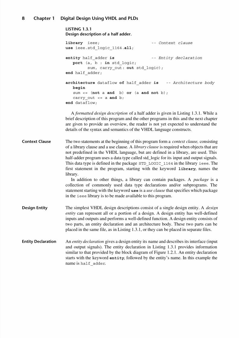
8/9/2019 VHDL for Engineers - Kenneth L. Short.pdf
http://slidepdf.com/reader/full/vhdl-for-engineers-kenneth-l-shortpdf 41/719
8 Chapter 1 Digital Design Using VHDL and PLDs
LISTING 1.3.1Design description of a half adder.
library ieee; -- Context clauseuse ieee.std_logic_1164.all;
entity half_adder is -- Entity declaration port (a, b : in std_logic; sum, carry_out: out std_logic);end half_adder;
architecture dataflow of half_adder is -- Architecture body begin
sum <= (not a and b) or (a and not b); carry_out <= a and b;end dataflow;
A formatted design description of a half adder is given in Listing 1.3.1. While abrief description of this program and the other programs in this and the next chapterare given to provide an overview, the reader is not yet expected to understand thedetails of the syntax and semantics of the VHDL language constructs.
Context Clause The two statements at the beginning of this program form a context clause, consistingof a library clause and a use clause. A library clause is required when objects that arenot predefined in the VHDL language, but are defined in a library, are used. Thishalf-adder program uses a data type called std_logic for its input and output signals.This data type is defined in the package STD_LOGIC_1164 in the library ieee. Thefirst statement in the program, starting with the keyword library, names thelibrary.
In addition to other things, a library can contain packages. A package is acollection of commonly used data type declarations and/or subprograms. Thestatement starting with the keyword use is a use clause that specifies which packagein the ieee library is to be made available to this program.
Design Entity The simplest VHDL design descriptions consist of a single design entity. A design
entity can represent all or a portion of a design. A design entity has well-definedinputs and outputs and performs a well-defined function. A design entity consists of two parts, an entity declaration and an architecture body. These two parts can be
placed in the same file, as in Listing 1.3.1, or they can be placed in separate files.
Entity Declaration An entity declaration gives a design entity its name and describes its interface (inputand output signals). The entity declaration in Listing 1.3.1 provides informationsimilar to that provided by the block diagram of Figure 1.2.1. An entity declarationstarts with the keyword entity, followed by the entity’s name. In this example thename is half_adder.

8/9/2019 VHDL for Engineers - Kenneth L. Short.pdf
http://slidepdf.com/reader/full/vhdl-for-engineers-kenneth-l-shortpdf 42/719
Section 1.3 VHDL Design Description 9
Ports A design entity’s input and output signals are called ports and are listed in the entitydeclaration following the keyword port. The half-adder’s inputs are a and b. Itsoutputs are sum and carry_out.
Port Data Types The type of data each port transfers is also specified. A signal’s data type deter-mines the values the signal may have and the operations that can be performed onthose values. The data carried by the half-adder’s input and output ports is typestd_logic.
Type std_logic provides nine different values to represent a logic signal. Thisallows a more detailed representation of a logic signal’s state than does type bit. Bothtypes include the values '0' and '1'. Type std_logic is discussed in detail in Chapter 3.Until then we will only be using the '0' and '1' values from std_logic’s nine possiblevalues.
Architecture Body An architecture body starts with the keyword architecture followed by the namegiven to the architecture. In this example, the architecture’s name is dataflow.Following the keyword of is the name of the entity declaration with which the archi-tecture is associated.
A design entity’s architecture describes either the entity’s behavior or its structure.In Listing 1.3.1, the architecture is written in a style called dataflow. Dataflow styledescribes a system’s behavior in terms of how data flows through the system. Eachoutput in Listing 1.3.1 is defined by a concurrent signal assignment statement:
sum <= (not a and b) or (a and not b);carry_out <= a and b;
The and, or, and not keywords in these statements are VHDL logical operators, notactual gates. In a physical implementation, each logical operation might, in fact, besynthesized using AND, OR, and NOT gates or by other types of logic gates (such asNAND gates) or by other logic elements, such as multiplexers.
Concurrent SignalAssignmentStatements
Signal assignment statements are unique to HDLs. Each of the previous concurrent
signal assignment statements assigns a new value to the signal on the left-hand sideof the signal assignment symbol (<=) whenever there is an event on one of thesignals on the right-hand side of the assignment symbol. The signal assignmentstatement is said to be sensitive to the signals on the right-hand side of thestatement.
The symbol <= is read as “gets.” So, the second assignment statement in Listing1.3.1 is read as ''carry_out gets a and b.'' Delimiters that consist of two adjacentspecial characters, such as the signal assignment symbol (<=), are called compound
delimiters.
8/9/2019 VHDL for Engineers - Kenneth L. Short.pdf
http://slidepdf.com/reader/full/vhdl-for-engineers-kenneth-l-shortpdf 43/719
10 Chapter 1 Digital Design Using VHDL and PLDs
Execution Orderof ConcurrentStatements
A concurrent signal assignment statement executes only in response to an event onone or more of the signals to which it is sensitive. The order of execution of concurrent signal assignment statements is solely determined by the order of eventson the signals to which the concurrent statements are sensitive.
In Listing 1.3.1, if there is an event on signal a, both assignment statements are
executed simultaneously to determine new values for sum and carry_out. Thesestatements are called concurrent because they allow the possibility of simultaneousexecution, which they must if they are going to model the operation of logic circuits.In our half adder, gates compute the two outputs simultaneously, not sequentially.
The concept of concurrent statements in VHDL is critically important. It creates adistinction between VHDL, or any HDL, and the sequential execution of statementsin a conventional programming language. This distinction must always be kept inmind when interpreting or writing a VHDL description.
Sequential
Statements
VHDL also has sequential statements, like those in conventional programming
languages. VHDL’s sequential statements can only appear inside a process statementor a subprogram. As a result, when reading a program it is easy to determine from itslocation whether a statement is concurrent or sequential. A process statement is aconcurrent statement that contains a sequence of sequential statements. An exampleof a process statement is seen in Section 1.5 of this chapter and process statementsare discussed in detail in Chapter 5. The half-adder program of Listing 1.3.1 containsno sequential statements.
Design DescriptionCompilation
A VHDL design description is compiled like a program written in a conventionalprogramming language, such as C++ or Ada. VHDL compilers are sometimes
called analyzers. The term “analyze” means to check a design file for syntax andstatic semantic errors before it is simulated. This term is sometimes used instead of the term “compile,” because compiling typically means to generate executableobject code. In contrast, code generation for VHDL was initially associated onlywith simulation. Analyzed VHDL code is stored in an intermediate form in alibrary for subsequent simulation. However, the distinction between the termscompile and analyze is often not made. In this book the two terms are used inter-changeably.
Syntax Errors Syntax errors are violations of the language grammar. For example, each entity
declaration must be terminated with an end statement.
Semantic Errors Every programming language attaches specific meanings to its language constructs.Semantic errors are violations of the meaning of the language.
Static SemanticErrors
Static semantic errors are errors in meaning that can be detected by a compilerbefore a simulation is performed. For example, if we have a signal assignment

8/9/2019 VHDL for Engineers - Kenneth L. Short.pdf
http://slidepdf.com/reader/full/vhdl-for-engineers-kenneth-l-shortpdf 44/719
Section 1.4 Verification Using Simulation 11
statement that assigns the value of a signal of type bit to a signal of type std_logic,we have a type-conflict static semantic error.
Dynamic SemanticErrors
In contrast, dynamic semantic errors can only be detected during simulation. Forexample, if we have a signal assignment statement where the left-hand and right-hand sides are the same type, but during execution the computed value of the right-hand side is outside the allowed range of values for that type, we have a dynamicerror.
We must find and remove all syntax and static semantic errors from a designdescription during compilation. This is accomplished by correcting the offendingstatements using an editor. Afterward, dynamic semantic errors are detected andcorrected during simulation.
1 .4 VE RI FI CA TI ON U SI NG S IM UL AT IO N
Before considering the next group of design flow phases, lets examine the impor-tance of simulation. When using VHDL, a simulator is the primary development,verification, and debugging tool.
Verification Verification is the process used to demonstrate the correctness of a design. We verifythat our design description meets its functional and timing specifications before thetarget PLD is programmed. Generally speaking, verification using simulation can showthe existence of errors in a design, but cannot prove that a design is correct. The process
of verification often consumes a significant percentage of the total design effort.
Simulation forVerification andDebugging
A VHDL simulator can execute a design description’s source code. The simulatorallows input values to be applied to the design description. In response, the simulatorcomputes the corresponding output values by executing statements in the designdescription.
When errors are encountered during a simulation, we can use the simulator’sdebugging features to find and correct the source of the errors in the designdescription. Once modified, a design description must be compiled and simulatedagain to verify that the errors have indeed been corrected.
Kinds ofSimulation
Simulation is performed during three different phases of the design flow (Figure1.1.1). Each simulation phase has a particular purpose and uses a different VHDLmodel of the same design entity:
• Functional simulation: we simulate our VHDL design description. Thissimulation is performed to verify that the system we described meets thefunctional requirements of its specification.

8/9/2019 VHDL for Engineers - Kenneth L. Short.pdf
http://slidepdf.com/reader/full/vhdl-for-engineers-kenneth-l-shortpdf 45/719
12 Chapter 1 Digital Design Using VHDL and PLDs
• Post-synthesis (gate-level) simulation: we simulate the synthesized VHDLnetlist. This netlist is a gate-level VHDL model of the synthesized logic. It isautomatically generated by the synthesizer. This simulation is performed toverify that the synthesized logic is functionally correct.
• Timing (post-route) simulation: we simulate the VHDL timing model of the
synthesized logic mapped to the target PLD. The VHDL timing model isautomatically generated by the place-and-route tool. This simulation isperformed to verify that the synthesized logic, as mapped to the target PLD,meets all timing constraints.
Later in this chapter, a separate section is devoted to each of these kinds of simulation.Prior to those sections, we consider how stimulus is provided to the model of thedesign entity during a simulation.
SimulationStimulus
A simulator requires a sequence of input values (stimulus) to apply to the VHDLmodel being verified. If an appropriate sequence of input values is created, it can be
used for all three kinds of simulation. There are three approaches to generatingstimulus: interactive (manual), command line, and testbench.
InteractiveSimulation
An interactive simulator allows us to manually apply a stimulus. The simulatorexecutes the design description using the input values applied and computes thecorresponding output values.
Waveform Viewer Waveforms representing the simulation model’s input and output values as a functionof time are displayed using the simulator’s waveform viewer. The waveform viewer
allows us to see transitions of multiple signals over time. We can zoom in or out toview selected time periods and measure the time between signal transitions. We candisplay bus signals as bits, hexadecimal numbers, or symbolic values. We can verifythat the simulated design meets its specification by visually examining the waveforms.
For simple designs, interactive simulation is adequate. For designs with morethan a few inputs, applying a comprehensive stimulus interactively becomes tediousand time-consuming. Furthermore, if the design description is modified, the entirestimulus has to again be manually applied to the modified design.
Command LineSimulation
Most simulators include a command line stimulus language. Commands in thestimulus language allow us to specify input waveforms. These commands can beentered interactively or placed in a file and executed. Using commands placed in afile makes it easy to reapply a stimulus after a design is modified. However, thisapproach is inefficient if the stimulus to be applied is complex. In addition, asimulator’s stimulus language is simulator specific and, therefore, not portable toother simulators.
The most powerful and portable approach to generating a stimulus is to use atestbench written in VHDL. This approach is described in the next section.

8/9/2019 VHDL for Engineers - Kenneth L. Short.pdf
http://slidepdf.com/reader/full/vhdl-for-engineers-kenneth-l-shortpdf 46/719
Section 1.5 Testbenches 13
1 . 5 TE ST BE N C H E S
We use the next four phases to verify the functional correctness of our designdescription:
• Develop verification plan
• Write VHDL testbench
• Compile testbench
• Functional simulation
Verification Plan Verification requires planning based on the system’s requirements and specificationdocuments. The results of this planning are documented in a verification plan. Forcomplex systems this plan is a substantial document requiring significant effort.
Even a very simple system requires some thought as to how it should be verified.
Often, the greatest difficulty in conducting a successful verification is determining anappropriate stimulus to apply and the output responses to be expected. The stimulusvalues applied must cover all of the circumstances in which the design will be used.
Testbench A testbench is a VHDL program that applies a predetermined stimulus to a designentity during simulation. A testbench can be written to also verify the output valuesproduced by the design entity. If there is a discrepancy between the expected and theactual output values, the testbench generates an error message. A testbench is basicallya stimulus–response system.
UUT The design entity being verified is usually called the unit under test (UUT). Strictlyspeaking, testing refers to the process of determining whether a design was manufac-tured correctly. For example, each system manufactured would be individuallytested. In contrast, verification is performed to determine whether a design meets itsspecifications, before it is manufactured in quantity. However, use of the term UUT,from manufacturing testing, has been carried over to verification. Other terms usedare device under test (DUT), design under test (DUT), device under verification(DUV), and module under test (MUT).
A testbench is also a design entity, it consists of a testbench entity declaration andits associated architecture body. A simple testbench architecture body contains:
• An instance of the UUT• Signals mapped to the UUT’s ports
• A process statement that applies stimulus to the UUT, via the signals
A testbench completely encloses its UUT and simulates the environment in whichthe design will operate.
The relationship between the half-adder UUT and its testbench is illustrated inFigure 1.5.1.

8/9/2019 VHDL for Engineers - Kenneth L. Short.pdf
http://slidepdf.com/reader/full/vhdl-for-engineers-kenneth-l-shortpdf 47/719
14 Chapter 1 Digital Design Using VHDL and PLDs
A testbench is entirely self-contained; it has no inputs or outputs. Statements inthe testbench’s architecture body apply stimulus values to signals that connect to theUUT’s inputs. Other statements monitor the output values from the UUT.
UUT Models forDifferent Kindsof Simulations
For a functional simulation, our VHDL design description is the UUT. For a post-synthesis simulation, the VHDL netlist model (the synthesized gate-level logic) isthe UUT. For a timing simulation, the VHDL timing model (produced by the place-and-route tool) is the UUT.
Half-adderTestbench
A testbench for the half adder of Listing 1.3.1 is given in Listing 1.5.1. This programcontains a design entity named testbench with an architecture body namedbehavior. Its entity declaration indicates that design entity testbench has noinputs or outputs.
LISTING 1.5.1Testbench for a half adder.
library ieee;use ieee.std_logic_1164.all;
entity testbench is
end testbench;
architecture behavior of testbench is
-- Declare signals to assign values to and to observe signal a_tb, b_tb, sum_tb, carry_out_tb : std_logic;
begin
-- Create an instance of the circuit to be tested uut: entity half_adder port map(a => a_tb, b => b_tb, sum => sum_tb, carry_out => carry_out_tb);
FIGURE 1.5.1
Conceptual relationship of the half-adder UUT to its testbench.
a sum
b carry_outHalf Adder carry_out_tb
sum_tba_tb
b_tb
Testbench
Stimulus
Generator
Response
Monitor
UUT

8/9/2019 VHDL for Engineers - Kenneth L. Short.pdf
http://slidepdf.com/reader/full/vhdl-for-engineers-kenneth-l-shortpdf 48/719
Section 1.5 Testbenches 15
-- Define a process to apply input stimulus and test outputstb : process
constant period: time := 20 ns;
begin -- Apply every possible input combination
a_tb <= '0'; --apply input combination 00 and check outputs b_tb <= '0'; wait for period; assert ((sum_tb = '0') and (carry_out_tb = '0')) report "test failed for input combination 00" severity error;
a_tb <= '0'; --apply input combination 01 and check outputs b_tb <= '1'; wait for period; assert ((sum_tb = '1') and (carry_out_tb = '0')) report "test failed for input combination 01" severity error;
a_tb <= '1'; --apply input combination 10 and check outputs b_tb <= '0'; wait for period; assert ((sum_tb = '1') and (carry_out_tb = '0')) report "test failed for input combination 10" severity error;
a_tb <= '1'; --apply input combination 11 and check outputs b_tb <= '1'; wait for period; assert ((sum_tb = '0') and (carry_out_tb = '1')) report "test failed for input combination 11" severity error;
wait; -- indefinitely suspend process end process;end;
In the declarative part of the architecture body (between keyword architecture
and the first begin keyword), signals used to provide connections between the half adder and the testbench are declared. In this example, these signals are named usingthe name of the UUT port they connect to followed by the suffix ''_tb.''
Following the begin keyword, UUT half_adder is instantiated and its connec-tions to the signals of the testbench are defined by a port map.
SequentialStatementsin a Process
Starting with the keyword process, a process named tb is defined. This processconsists of signal assignment statements interspersed with wait statements andassertion statements. The statements in a process are sequential statements. They areexecuted in sequence, like statements in a conventional programming language. The

8/9/2019 VHDL for Engineers - Kenneth L. Short.pdf
http://slidepdf.com/reader/full/vhdl-for-engineers-kenneth-l-shortpdf 49/719
16 Chapter 1 Digital Design Using VHDL and PLDs
process statement and the sequential statements used in a process are discussed indetail in Chapter 5. The brief discussion of these constructs at this point is just toprovide some insight into the nature of a testbench.
Process tb simply applies, over time, four combinations of values to the signalsconnected to the UUT’s two inputs. These are the four possible combinations of the
two values '0' and '1' from the set of nine std_logic values. After each input combi-nation is applied, the process waits 20 ns before verifying the outputs and applyingthe next input combination. This wait period would normally be determined basedon timing constraints stated in the system specification.
Using AssertionStatements toVerify Outputs
Process tb uses assertion statements, which start with the keyword assert, toverify that the UUT’s outputs have their expected values. If there is a differencebetween a simulated output value and the expected output value, an assertionstatement causes the simulator to display an error message.
For example, after the input combination a_tb = '0' and b_tb = '1' is applied, anassertion statement verifies that sum_tb = '1' and carry_out_tb = '0'. If, duringthe simulation, this is not actually the case, the assertion statement causes thesimulator to display the message ''test failed for input combination 01''.
A testbench should be written for every VHDL design. The testbench can even bewritten prior to writing the design description and serve as part of the specification.
As seen in Figure 1.1.1, once the design description and testbench have beenwritten, the remaining phases in the design flow, excluding PLD selection, are all,essentially, automated. Compared to traditional digital design methodologies, thissignificantly simplifies and speeds up the design process.
While it is appropriate that the testbench be written in parallel with, or evenbefore, writing the design description, this book focuses first on writing design
descriptions. After an adequate subset of VHDL language constructs have beencovered, the writing of testbenches is discussed in several chapters.
1 .6 F UN CT IO NA L ( BE HA VI OR AL ) S IM UL AT IO N
The same simulator is used to perform all three kinds of simulation. But, as previ-ously stated, the VHDL model used as the UUT is different for each. When theoriginal VHDL design description is used, the simulation is a functional simulation.
FunctionalSimulation
A functional simulation simulates the design description to verify its logical correct-ness. None of the propagation delays that affect signals in a target PLD can be observedin a functional simulation. Functional simulation is a necessity for complex designs,because early detection of logical errors saves significant time and expense. Functionalsimulation of simple designs is an extremely valuable aid in learning VHDL.
The design flow for the VHDL/PLD design methodology is presented in greaterdetail in this section and Sections 1.9 and 1.10. Each of these sections has a figurethat represents a portion of the design flow from Figure 1.1.1 shown in greater detail.

8/9/2019 VHDL for Engineers - Kenneth L. Short.pdf
http://slidepdf.com/reader/full/vhdl-for-engineers-kenneth-l-shortpdf 50/719
Section 1.6 Functional (Behavioral) Simulation 17
Each figure includes one of the three types of simulation. Taken together, these threefigures form a detailed flowchart of the entire design flow.
The first portion of the detailed design flow is shown in Figure 1.6.1. Phases areshown as rectangles. The software tool used in each phase is shown as a shaded androunded rectangle to the right of the associated phase.
FIGURE 1.6.1
Detailed view of functional simulation portion of VHDL/PLD design flow.
RequirementsAnalysis
Write (or Edit)VHDL DesignDescription
CompileDesign
Description
FunctionalSimulation
SimulationPassed?
Write (or Edit)VHDL
Testbench
CompileTestbench
1
Editor Editor
Compiler Compiler
Simulator
VHDL design
description
source file
compiled source
file
1 No
VHDL testbench
source file
compiled
testbench file
designphase tool
legend
functionally
verified design
description
DevelopSpecification
DevelopVerification
Plan
2
Yes

8/9/2019 VHDL for Engineers - Kenneth L. Short.pdf
http://slidepdf.com/reader/full/vhdl-for-engineers-kenneth-l-shortpdf 51/719
18 Chapter 1 Digital Design Using VHDL and PLDs
In Figure 1.6.1, the testbench is shown as being written in parallel with the designdescription. Design teams often write the design description and testbench in parallel.
Detecting Dynamic
Semantic Errors
Functional simulation is the time for logically debugging our design description and
detecting dynamic semantic errors. Since the design description is the UUT, changesin signal values during the functional simulation map directly to statements in oursource code.
SimulatorDebuggingCapabilities
Typical debugging capabilities provided by a simulator allow us to:
• Single step through source code statements
• Set breakpoints on source code statements
• Set breakpoints on signal or variable changes in value
• Monitor (watch) signal and variable values
Simulator OutputWaveforms
Waveforms from the functional simulation of the half adder are shown in Figure1.6.2. The signals displayed are those used to connect the UUT to the testbench.Because this is a functional simulation, the waveforms do not show any delay froman input change to a corresponding output change. That is, as soon as a UUT inputchanges, its outputs respond instantaneously.
1 .7 P RO GR AM MA BL E L OG IC D EV IC ES ( PL DS )
To proceed further in the design flow we must select a target PLD. This sectionprovides a brief introduction to PLDs.
Fixed-Function ICs Prior to the advent of PLDs, digital systems were implemented by interconnectingoff-the-shelf fixed-function ICs. Small-scale integration (SSI) ICs provided discretegates and flip-flops. Medium-scale integration (MSI) and large-scale integration
FIGURE 1.6.2
Waveforms from the functional simulation of the half-adder description.

8/9/2019 VHDL for Engineers - Kenneth L. Short.pdf
http://slidepdf.com/reader/full/vhdl-for-engineers-kenneth-l-shortpdf 52/719
Section 1.7 Programmable Logic Devices (PLDs) 19
(LSI) ICs provided more complex combinational and sequential functional subsystems.The specific functions implemented by a fixed-function IC are determined by the ICmanufacturer and cannot be changed by the user.
PLDs The advent of programmable logic devices (PLDs) provided a more flexible way to
implement a digital system. PLDs come in a wide variety of architectures and logiccapacities. The term PLD is used generically in this book and, therefore, includes allICs used for implementing digital hardware that are programmed by the user.
SPLDs, CPLDs,and FPGAs
PLDs are broadly classified based on their architectures as simple PLDs (SPLDs),complex PLDs (CPLDs), and field programmable gate arrays (FPGAs). Each of these classes of devices has manufacturer-specific variants.
Logic Capacity A PLD’s logic capacity is usually specified in terms of the number of two-inputNAND gate functional equivalents it provides.
A SPLD has a basic AND/OR array architecture and a maximum logic capacityof approximately 500 gates. A CPLD consists of multiple SPLD blocks on a singleIC. Also included on a CPLD is a programmable interconnect matrix that allows theintegrated SPLD blocks to be interconnected. The maximum logic capacity for aCPLD is approximately 60,000 gates.
FPGA architectures differ significantly from those of SPLDs and CPLDs. FPGAgate capacities start as low as 10,000 gates. Some FPGAs’ logic capacities exceed8,000,000 gates.
Logic capacity ranges for the different classes of PLDs tend to overlap near theirboundaries. For CPLDs and FPGAs, the upper bounds of these ranges continue toincrease over time as IC process technology advances.
AND/OR Arrays To illustrate the concept of a PLD we consider a combinational SPLD. Conceptually,this SPLD consists of an array of AND gates followed by an array of OR gates. Thelogical structure of such an architecture is shown in Figure 1.7.1(a).
Buffered Inputs Inputs to the SPLD are internally buffered, producing the normal and complementforms of each input signal. These signals appear on the vertical lines to the left of theAND gates in Figure 1.7.1(a).
AND Array The vertical lines from the input buffers intersect horizontal lines that representinputs to the AND gates. Each AND symbol has a single horizontal input line calleda product line. The vertical lines from the input buffers, the product lines, and ANDgates comprise the AND array.
Product Line A product line is a single line that concisely represents all of the inputs to an ANDgate. For example, each AND gate in Figure 1.7.1 is a four-input AND. Therefore,each product line actually represents four inputs.
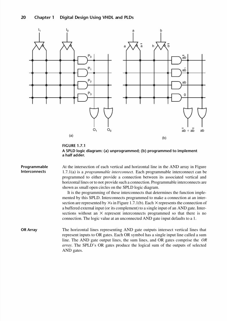
8/9/2019 VHDL for Engineers - Kenneth L. Short.pdf
http://slidepdf.com/reader/full/vhdl-for-engineers-kenneth-l-shortpdf 53/719
20 Chapter 1 Digital Design Using VHDL and PLDs
ProgrammableInterconnects
At the intersection of each vertical and horizontal line in the AND array in Figure1.7.1(a) is a programmable interconnect. Each programmable interconnect can beprogrammed to either provide a connection between its associated vertical andhorizontal lines or to not provide such a connection. Programmable interconnects areshown as small open circles on the SPLD logic diagram.
It is the programming of these interconnects that determines the function imple-mented by this SPLD. Interconnects programmed to make a connection at an inter-section are represented by ×s in Figure 1.7.1(b). Each × represents the connection of a buffered external input (or its complement) to a single input of an AND gate. Inter-sections without an × represent interconnects programmed so that there is no
connection. The logic value at an unconnected AND gate input defaults to a 1.
OR Array The horizontal lines representing AND gate outputs intersect vertical lines thatrepresent inputs to OR gates. Each OR symbol has a single input line called a sumline. The AND gate output lines, the sum lines, and OR gates comprise the OR
array. The SPLD’s OR gates produce the logical sum of the outputs of selectedAND gates.
FIGURE 1.7.1
A SPLD logic diagram: (a) unprogrammed; (b) programmed to implementa half adder.
(a)(b)
ba
a
0
ab
b
ab
ab
a b
ab
ab ab
I0
O0O1
P0
P1
P2
P3
I1

8/9/2019 VHDL for Engineers - Kenneth L. Short.pdf
http://slidepdf.com/reader/full/vhdl-for-engineers-kenneth-l-shortpdf 54/719
Section 1.8 SPLDs and the 22V10 21
Sum Line A sum line is a single line that concisely represents all of the inputs to an OR gate. Theparticular SPLD of Figure 1.7.1 has a fixed OR array that cannot be programmed. Thefixed connections in this OR array are indicated by solid circles at the intersections of its horizontal and vertical lines.
The SPLD in Figure 1.7.1(b) represents the SPLD in Figure 1.7.1(a) programmed
to implement a half adder. The physical programming of a SPLD is accomplishedusing information in the configuration file produced by the place-and-route tool. TheAND/OR architecture of this PLD is ideal for implementing the required sum-of-products Boolean functions.
ProgrammableArray Logic (PAL)
A SPLD with a programmable AND array and a fixed OR array, as in Figure 1.7.1,is more specifically referred to as a programmable array logic (PAL).
1 . 8 SP LD S A ND T HE 22 V1 0
Designs in the early chapters of this book are of low logic complexity and can beimplemented using a SPLD. This section provides an overview of an actual SPLD thatcould be used as the target PLD for these designs. Since the majority of today’s SPLDsare based on the PAL architecture, this section focuses on the 22V10 PAL-type SPLD.
ContemporarySPLDs
There are two major differences in today’s PAL-type SPLDs and the conceptual PALshown in Figure 1.7.1(a).
Erasable PLDs First, today’s SPLDs use electrically erasable and reprogrammable interconnects.
Such an interconnect uses a floating gate transistor structure similar to that used inan EEPROM.
Erasing returns each programmable interconnect to its unprogrammed state. Erasable PLDs have the advantage that if a logic error is found in a design after thePLD is programmed or if features need to be added, the previously loaded configu-ration information can be erased. After the design error is corrected or features areadded in the design description, the modified design is verified. The PLD is thenreprogrammed using the new configuration information. Use of reprogrammablePLDs allows us to rapidly and economically iterate design changes.
Electrically erasable interconnects have fast erase times, typically less than 100ms. The minimum number of program/erase operations that can be performed onsuch a SPLD is typically greater than 10,000. Data retention typically exceeds 20years. A SPLD might typically be programmed from one to 20 times during devel-opment. During production, a SPLD is normally programmed only once.
Output LogicMacrocells
The second major difference in today’s PAL-type SPLDs and the conceptual PLDshown in Figure 1.7.1(a) is that a programmable output logic macrocell (OLMC) isconnected to the output of each OR gate. The output of each OLMC connects to a

8/9/2019 VHDL for Engineers - Kenneth L. Short.pdf
http://slidepdf.com/reader/full/vhdl-for-engineers-kenneth-l-shortpdf 55/719
22 Chapter 1 Digital Design Using VHDL and PLDs
pin of the PAL. Use of OLMCs allows each pin to be independently programmed toimplement any one of three different I/O structures. An OLMC can be configured tomake the pin that it connects to an output, input, or bidirectional. An OLMC also
contains a flip-flop, so that the output of the OR gate can be stored. This allows aPAL to be used to implement either combinational or sequential systems.An OLMC is represented in Figure 1.8.1 as the logic inside the dashed block.
The data input to the OLMC is the output from the OR gate that sums the productterms from the AND array. The AND gate at the top of the diagram is an outputenable product term that controls the three-state inverting output buffer. Theproduct line for this AND gate can be programmed so that its output is fixed at 0,disabling the three-state buffer, to configure the I/O pin as an input. In contrast, if this gate’s output is fixed at 1, enabling the three-state buffer, the I/O pin isconfigured as an output. Alternatively, since this AND gate’s product line is part of the AND array, its output can be a function of the PAL’s inputs, allowing the I/O pin
to be bidirectional.
CombinationalMacrocell Output
In the OLMC of Figure 1.8.1, the configuration of the output is controlled by themacrocell’s four-input multiplexer. This multiplexer allows the D flip-flop in themacro cell to be bypassed. It also allows the output’s polarity to be specified. The multi-plexer’s select inputs are from two programmable connections, S1 and S0. Theseconnections are called configuration bits. Each OLMC has its own configuration bits.
FIGURE 1.8.1
Output logic macrocell.
CLK
MUX
S1S0
MUX
QD
10
11
00
01
0
1
Q

8/9/2019 VHDL for Engineers - Kenneth L. Short.pdf
http://slidepdf.com/reader/full/vhdl-for-engineers-kenneth-l-shortpdf 56/719
Section 1.8 SPLDs and the 22V10 23
For a combinational active-high output , S1S0 is made 11. This selects the inverted outputof the OR gate as the input to the inverting three-state buffer that drives the I/O pin.
For a combinational active-low output , S1S0 is made 10. Under this condition, theoutput of the OR gate is directly input to the inverting output buffer.
In both the previous cases S1 is 1, so the two-input multiplexer at the lower left of
the macrocell feeds the signal at the I/O pin back, in both its normal and complementforms, as inputs to the AND array.
RegisteredMacrocell Output
A registered output is one derived from an OLMC’s flip-flop. For a registered active-
high output , S1S0 is made 01 and the Q output of the D flip-flop is input to theinverting output buffer. For a registered active-low output , S1S0 is made 00 and the Qoutput of the D flip-flop is directly input to the inverting output buffer. For eitherregistered output, S1 is 0, and the Q output of the flip-flop is fed back, in its normaland complement forms, as inputs to the AND array.
Each output logic macrocell is independently programmable, providing substantial
flexibility. Like the reprogrammable interconnects in the AND gate array, the configu-ration bits S1 and S0 are also reprogrammable.
ProgrammableOutput Polarity
It is clear from the previous discussion that an OLMC provides versatility, but how isthis versatility used and why is it advantageous?
When implementing a combinational function, the OLMC allows either thesum-of-products function or its complement to appear at its output pin. SomeBoolean sum-of-product functions are most efficiently implemented in theirnormal (true) form. Others are more efficiently implemented in their complementform. That is, either the normal or complement form of a particular function might
require fewer product terms. A function that is a wide OR function is mostefficiently implemented in a SPLD-type architecture as the complement of thecomplement of the function.
For example, the complement of a large sum of individual terms may beexpressed as a single product term. Consider a function that is the OR of 18 inputs.To implement this function directly in the programmable AND–fixed OR archi-tecture of a PAL requires 18 AND gates, each with only one of its inputs used. Inother words, each input to the OR gate requires a product term consisting of a singleliteral. The output OR gate sums these 18 product terms to realize the function.Assume that you had a SPLD where the most product terms that can be ORedtogether as input to an OLMC is 16. This function requiring 18 AND gates cannot bedirectly implemented in this SPLD using a single output.
However, by application of DeMorgan’s Law, the OR of 18 inputs is equivalent tothe complement of the AND of the complements of each of the 18 inputs. Since eachinput is available in its complement form in the AND array of a SPLD, all we need isa single AND gate with at least 18 inputs. This gives the complement of the desiredfunction at the output of the OR gate. The output of the OR gate is then comple-mented in the OLMC to obtain the desired function.

8/9/2019 VHDL for Engineers - Kenneth L. Short.pdf
http://slidepdf.com/reader/full/vhdl-for-engineers-kenneth-l-shortpdf 57/719
24 Chapter 1 Digital Design Using VHDL and PLDs
With programmable output polarity, synthesis and place-and-route software canperform logic optimization on an expression and its complement and use the formthat requires the fewest logic resources.
Popular PAL-type
SPLDs
There are a number of popular PAL-type SPLDs that find widespread use. Part
numbers for these devices typically start by designating the total number of I/Os.This is followed by a letter indicating the type of flip-flop or logic in the OLMC.Next is a number indicating the maximum number of outputs. A hyphen thenprecedes a number indicating the SPLD’s speed. Other letters following the speedmay indicate power level, package type, and temperature grade.
The most popular SPLDs are the 16V8, 18V10, 20V8, 22V10, and 26V12. Themost popular SPLD from this group is the 22V10. The “V” stands for versatile,meaning that the device contains OLMCs allowing a variety of I/O configurations.Versions of the previous devices are available from manufacturers such as Atmel,Cypress, and Lattice Semiconductor. Data sheets and application notes providingdetails on these devices are available from the manufacturers’ web sites.
The 22V10 SPLD A block diagram of a 22V10 is shown in Figure 1.8.2. A 22V10 has 12 dedicatedinput pins, shown on the left of the diagram, and 10 input/output (I/O) pins, shownon the right. I/O pins are pins that can be configured as either inputs or outputs. Onemanufacturer rates this device as having a logic capacity of 500 gates.
The “22” in the designation 22V10 indicates that the device provides up to 22inputs. All 22 inputs are available only when all 10 I/O pins are configured as inputsand used along with the 12 dedicated input pins. The “10” in the designation indicatesthat as many as 10 outputs are available. This situation exists when all of the I/O pinsare configured as outputs. Practically speaking, only 21 inputs are available, since in
any useful application at least one I/O pin needs to be configured as an output.The 22V10’s logic diagram is shown in Figure 1.8.3. The pin numbers are those for
a 28-pin PLCC package. The 12 dedicated input pins are shown on the left side andbottom right side of this diagram. The input at pin 2 can be used as either the globalclock input to the D flip-flops or as an input to the AND array. Each input is buffered.The buffered normal and complement forms of each input are connected to separatecolumns, generating 24 columns. For example, the buffered normal and complementforms of the input at pin 3 are available on columns 4 and 5, respectively.
The other 20 columns are the normal and complement forms of signals either fedback from the 10 macrocells on the right side of the diagram or input from I/O pins
configured as inputs. Together these 44 columns provide the AND array the normaland complement forms of the 22 possible inputs.The rows of the AND array are the AND gate product lines. Each AND gate has 44
inputs. For each output, one AND gate, the output enable product term, is used tocontrol that output’s inverting three-state buffer. The remaining AND gates associatedwith an output provide the inputs to the OR gate that feeds the output’s OLMC.
Two other AND gates are shared by all the OLMCs. One controls the asynchronousresets to all the flip-flops in the OLMCs and the other controls their synchronous

8/9/2019 VHDL for Engineers - Kenneth L. Short.pdf
http://slidepdf.com/reader/full/vhdl-for-engineers-kenneth-l-shortpdf 58/719
Section 1.8 SPLDs and the 22V10 25
presets. All total, there are 132 AND gates, each with 44 inputs. Accordingly, the ANDarray is designated as 132 × 44 in Figure 1.8.2.
22V10 ProductTerm Distribution Not all of the 22V10’s OR gates have the same number of inputs (AND gateoutputs). This is seen clearly in the block diagram. This type of arrangement, calledvaried product term distribution, is based on the fact that in a typical applicationsome logic expressions require fewer product terms than others. If each OR gatesummed 16 product terms, for some outputs many product terms would go unused.
For example, the OR gate providing the output at pin 27 has 8 inputs and the OR gateproviding the output at pin 23 has 16 inputs (Figures 1.8.2 and 1.8.3). As a result, theoutput at pin 27 can implement a sum-of-products expression that is the sum of as many
FIGURE 1.8.2
Functional block diagram of a 22V10 SPLD. Courtesy of Lattice SemiconductorCorporation. All rights reserved.
P R O G R A M M A B L E
A N D - A R R A Y
( 1 3
2 X 4 4 )
I/O/Q
I/O/Q
I/O/Q
I/O/Q
I/O/Q
I/O/Q
I/O/Q
I/O/Q
I/O/Q
I/O/QSDOSDI
MODESCLK
I/CLK
I
I
I
I
I
I
I
I
I
I
RESET
PRESET
8
10
12
14
16
16
14
12
10
8
OLMC
OLMC
OLMC
OLMC
OLMC
OLMC
OLMC
OLMC
OLMC
OLMC
PROGRAMMING
LOGIC
I

8/9/2019 VHDL for Engineers - Kenneth L. Short.pdf
http://slidepdf.com/reader/full/vhdl-for-engineers-kenneth-l-shortpdf 59/719

8/9/2019 VHDL for Engineers - Kenneth L. Short.pdf
http://slidepdf.com/reader/full/vhdl-for-engineers-kenneth-l-shortpdf 60/719
Section 1.9 Logic Synthesis for the Target PLD 27
as 8 product terms, each of 22 variables, and the output at pin 23 can implement a sum-of-products expression that is the sum of as many as 16 product terms, each of 22 variables.
22V10 Output LogicMacrocells
The 22V10’s OLMCs are similar to that shown in Figure 1.8.1. It can be configuredto provide a combinational active-low, combinational active-high, registered active-low, or registered active-high output. The flip-flops in all 10 OLMCs share a commonclock, asynchronous reset, and synchronous preset. The asynchronous reset andsynchronous preset are each derived from product terms in the AND array. Therefore,they can be an AND function of any of the inputs.
While the 22V10 has considerable logic capacity (500 gate equivalents) andversatility (provided by its OLMCs), it is still a SPLD, and as such is among thesimplest and least capable PLDs.
1 .9 L OG IC SY NT HE SI S F OR T HE TA RG ET PL D
The next group of phases is performed to synthesize logic for the target PLD. Thesephases are:
• Select PLD
• Synthesize logic
• Post-synthesis simulation
This portion of the design flow starts with selection of the target PLD, as shown inFigure 1.9.1.
Selecting theTarget PLD
A PLD must be selected that has sufficient logic capacity to implement the logic tobe synthesized. The selected PLD is called the target PLD. The target PLD must alsobe fast enough to meet the system’s timing requirements. To optimally make thisselection, we must have a good knowledge of PLDs and their architectures.
For complex designs, a PLD is typically selected such that no more than approxi-mately 80 to 90% of its resources are expected to be used. This provides extraresources to ensure a successful routing and possibly allow additional features to beadded later. For our half-adder design, very little logic capacity is required, so a22V10 SPLD is a more than adequate choice.
Logic Synthesis Once the target PLD has been selected, a synthesizer is used to synthesize the logicdescribed by the design description. Synthesis is the process of automatically trans-lating a VHDL design description to logic. The synthesized logic is optimized interms of area (number of gates) and/or speed (number of gate levels).
It is important to keep in mind that while a synthesizer optimizes the logic itproduces, it can only translate the given VHDL description to hardware. If what isdescribed is an inferior solution to the original problem, the synthesized results willbe less than optimal.

8/9/2019 VHDL for Engineers - Kenneth L. Short.pdf
http://slidepdf.com/reader/full/vhdl-for-engineers-kenneth-l-shortpdf 61/719
28 Chapter 1 Digital Design Using VHDL and PLDs
A synthesizer requires two inputs: the design description file and the specificationof the target PLD.
Synthesizer The objective of a synthesizer is to synthesize logic that behaves identically to the
simulated behavior of the design description. In effect, a synthesizer translates adesign description into a functionally equivalent gate-level logic implementation.
FIGURE 1.9.1
Detailed view of post-synthesis simulation portion of VHDL/PLD design flow.
Select TargetPLD
SynthesizeDesign
Description
Post SynthesisSimulation
SimulationPassed?
3
2
1
Synthesizer
Simulator
target PLD
selection
synthesized logic
VHDL netlist
Yes
No
compiled testbench
file
functionally
verified design
description
PostSynthesis
Simulation?Yes
No
EDIF post-
synthesis netlist

8/9/2019 VHDL for Engineers - Kenneth L. Short.pdf
http://slidepdf.com/reader/full/vhdl-for-engineers-kenneth-l-shortpdf 62/719
Section 1.9 Logic Synthesis for the Target PLD 29
A synthesizer generates the required Boolean equations. It automatically carriesout logic and state minimization and stores the simplified Boolean equations in anintermediate form. The output of the synthesizer is a gate-level logic description.
Gate-Level Logic A gate-level logic implementation is sometimes referred to as a register transfer level
(RTL) implementation. This level describes the logic in terms of registers and theBoolean equations for the combinational logic between the registers. Of course, for acombinational system there are no registers and the RTL logic consists only of combi-national logic. Register transfer logic is discussed in greater detail in Chapters 10, 11,and 15.
A synthesizer may include its own compiler to compile a design description intothe intermediate form used by the synthesizer. This compiler can highlight synthesiserrors in the source code. Not all VHDL language constructs can be synthesized.Some synthesis errors result from the use of constructs that can’t be synthesized.
Typically, a synthesizer performs three steps during synthesis:
1. Language synthesis: the design description is transformed into a represen-tation based on Boolean equations. These equations represent the intercon-nection of generic logic elements or functional blocks.
2. Optimization: algorithms apply the rules of Boolean algebra to optimize the logicfor area and/or speed. These optimizations are independent of the technology of the target PLD and produce a technology independent gate-level netlist.
3. Technology mapping: the logic is mapped to the target PLD using techniquesspecific to the target PLD’s architecture and further optimizations areperformed. This step corresponds to transforming the technology independentnetlist to a technology dependent netlist.
For our simple half adder, the logic that results from step 1 of the synthesis processis given in Figure 1.9.2.
FIGURE 1.9.2
RTL view of half-adder synthesized logic from synthesis step 1.
carry_out
sum
sum
un3_sum
sum_1
b
a
carry_out

8/9/2019 VHDL for Engineers - Kenneth L. Short.pdf
http://slidepdf.com/reader/full/vhdl-for-engineers-kenneth-l-shortpdf 63/719
30 Chapter 1 Digital Design Using VHDL and PLDs
The logic from step 3 is represented in Figure 1.9.3. This diagram includes inputand output buffers that are part of the target 22V10 SPLD architecture.
SynthesizerOutput
The synthesizer produces two output files: a VHDL netlist and a technology dependentgate-level netlist.
A netlist is a textual representation of the interconnection of logic elements.
VHDL Netlist A VHDL netlist is a design file that describes, in VHDL structural style, the connec-tivity of the optimized logic implemented using the target PLD’s primitives. TheVHDL netlist is used as the UUT model in a post-synthesis simulation.
Post-Synthesis
(Gate-Level)Simulation
To verify the synthesized logic, the VHDL netlist is used as the UUT in the testbench.
Simulation of the VHDL netlist is called post-synthesis simulation or gate-levelsimulation, since it simulates the structural interconnection of the gates and flip-flopssynthesized for a design. It verifies the functional operation of the synthesized logic.
The results from this simulation are compared with the results from the functionalsimulation of the design description. These results should be the same.
For post-synthesis simulation of our half adder, its design description is replaced asthe UUT model in the testbench by the VHDL netlist. This replacement is accomplishedby replacing the file that contains the design description of the half adder with the filegenerated by the synthesizer that contains the VHDL netlist of the synthesized logic.
If the synthesized logic is functionally correct, the post-synthesis simulationwaveforms will be the same as the functional simulation waveforms in Figure 1.6.2.
Simulators usually have a feature that allows waveforms from different simulationsto be compared. This makes it easy to compare waveform results from a post-synthesis simulation with those from the corresponding functional simulation.
SkippingPost-SynthesisSimulation
If a timing simulation is to be performed, post-synthesis simulation may beskipped. A timing simulation can simultaneously verify both the function andtiming of the synthesized logic, making post-synthesis simulation unnecessary.
FIGURE 1.9.3
Technology dependent view of half-adder synthesized logic from synthesis step 3.
carry_out
sum.OG_4.O
carry_out_0_and2.Ocarry_out.Ob.O
a.O
sum
b
a
8/9/2019 VHDL for Engineers - Kenneth L. Short.pdf
http://slidepdf.com/reader/full/vhdl-for-engineers-kenneth-l-shortpdf 64/719
Section 1.10 Place-and-Route and Timing Simulation 31
Accordingly, the activities related to post-synthesis simulation are shaded inFigure 1.9.1.
TechnologyDependent Netlist
A technology dependent netlist describes the connectivity of the optimized logic usingthe target PLD’s logic primitives. These primitives are the logic elements available in
the target PLD’s architecture. The technology dependent netlist is in a format readableby the PLD vendor’s place-and-route tool. Typically, the EDIF netlist format is used.
EDIF NetlistFormat
EDIF (Electronic Data Interchange Format) is a format issued by the ElectronicIndustries Association, as EIA-548. Its purpose is to provide a standard format fortransferring design information between EDA tools.
1 . 1 0 P L A CE - A ND - R O U TE A N D T I MI N G S I M U L A T I O N
The next phases are:
• Place and route logic to PLD
• Timing simulation
These phases are included in the last portion of the detailed VHDL/PLD design flowshown in Figure 1.10.1.
Place-and-RouteOperations
A place-and-route (or fitter ) tool is software used to automatically map or fit synthe-sized logic to a target PLD’s architecture. The place operation selects and configures
specific logic primitives in the PLD’s architecture for each logic primitive in thetechnology dependent netlist.The route operation determines the path for each connection between two logic
primitives and each connection between a logic primitive and a pin of the PLD. Theplace-and-route tool is usually obtained from the PLD vendor.
Place-and-RouteTool
A place-and-route tool takes as its inputs a technology dependent gate-level EDIFnetlist and constraint information such as pin assignments for port signals and timingconstraints.
The place-and-route tool maps the EDIF netlist into the PLD’s architecture bydetermining exactly which instance of each primitive logic element in the PLD’sarchitecture to use for each primitive in the synthesized logic. It also takes intoaccount such things as desired pin assignments for port signals and timing goals.
Pin Assignments In our half-adder design example we did not concern ourselves with the assignmentof input and output signals to specific pins of the PLD. The place-and-route tool canautomatically make these assignments. However, sometimes we want to make theseassignments ourselves, rather than depending on the place-and-route tool’s default

8/9/2019 VHDL for Engineers - Kenneth L. Short.pdf
http://slidepdf.com/reader/full/vhdl-for-engineers-kenneth-l-shortpdf 65/719
32 Chapter 1 Digital Design Using VHDL and PLDs
assignments. For example, if we modify some of the logic of a design and reprocess
the modified description, the place-and-route tool may assign the signals to differentpins. If the printed circuit board for the PLD has been laid out based on the previouspin assignments, we will have a problem.
A place-and-route tool allows us to specify pin assignments. The ability of theplace-and-route tool to achieve specified pin assignments and to maintain theseassignments after a design’s logic has been modified depends on the routingresources of the PLD.
FIGURE 1.10.1
Detailed view of timing simulation portion of VHDL/PLD design flow.
Place andRoute
SynthesizedLogic
TimingSimulation
SimulationPassed?
3
1 or 2
Place andRoute
Simulator
synthesized
logic EDIF
netlist
post-fit VHDL
timing model
Yes
No
compiled
testbench file
Program PLD
Done
configuration file
Verify PLD’sOperation

8/9/2019 VHDL for Engineers - Kenneth L. Short.pdf
http://slidepdf.com/reader/full/vhdl-for-engineers-kenneth-l-shortpdf 66/719
Section 1.10 Place-and-Route and Timing Simulation 33
User-DefinedAttributes
How pin assignments are specified depends on the particular place-and-route tool. Oneapproach is to use VHDL’s user-defined attribute feature. In addition to predefinedattributes, VHDL allows the user to define attributes. User-defined attributes areVHDL statements that we can include in our design description file. A user-definedattribute does not affect the semantics of the VHDL code. It is recognized only by the
EDA tool that defines it. These attributes are used to pass information to EDA toolsused in the design flow.
Synthesis and place-and-route tool vendors create their own “user”-definedattributes to allow us to specify information about how a design should be synthesizedor placed and routed. Such attributes are described in each tool’s documentation.
For example, attributes defined by Lattice Semiconductor to specify pin assign-ments for their SPLDs are placed in the entity declaration as shown in Listing 1.10.1.
These attributes are ignored by the compiler and synthesizer. However, they arepassed along to the place-and-route tool in the EDIF file generated by the synthe-sizer. Our design description examples usually do not include specification of pinassignments.
Place-and-RouteTool Outputs
A place-and-route tool generally produces three outputs: a chip report, a configu-ration file, and a VHDL timing model.
Chip Report The chip report documents which port signals are assigned to which PLD pins andhow much of the PLD’s logic capacity is used.
LISTING 1.10.1Use of attributes to specify assignment of ports to device pins.
library ieee;use ieee.std_logic_1164.all;
entity half_adder is
port (a, b : in std_logic; sum, carry_out: out std_logic);
attribute loc: string; -- pin assignment attribute attribute loc of a : signal is "P3"; -- pin assignments attribute loc of b : signal is "P4"; attribute loc of sum : signal is "P25"; attribute loc of carry_out : signal is "P24";
end half_adder;
architecture dataflow of half_adder is
begin
sum <= (not a and b) or (a and not b); carry_out <= a and b;end dataflow;

8/9/2019 VHDL for Engineers - Kenneth L. Short.pdf
http://slidepdf.com/reader/full/vhdl-for-engineers-kenneth-l-shortpdf 67/719
34 Chapter 1 Digital Design Using VHDL and PLDs
For example, the 22V10 SPLD is available in several packages including a 24-pindual-in-line package (DIP). As previously discussed, this chip has 12 dedicatedinputs and 10 I/O pins that can be configured as either inputs or outputs. The othertwo pins are power and ground. Our half adder requires only two input pins and twoI/O pins configured as outputs. Slightly less than 20% of the 22V10’s pins and logic
capacity are required. We could put four additional half adders in the same PLD, oruse the unused logic for other functions.
Configuration File The configuration file (programming file) contains the interconnection and configu-ration data necessary to program the PLD. This file specifies exactly which program-mable interconnects in the target PLD are to be programmed as connections andwhich are not.
VHDL TimingModel
The VHDL timing model is a file containing a structural-style VHDL program thatdescribes the logic and timing of the synthesized logic mapped to the target PLD.
This model includes information detailing the propagation delays of signals throughthe PLD.
Timing ParameterValues
The VHDL timing model uses a set of timing parameters to specify the propagationdelays of the PLD’s primitive elements. The timing parameter values are usuallypassed to the model using constants called generics. Actual generic values are eitherdefined directly in the timing model or specified in a separate file that is generated bythe place-and-route tool. If a separate file is used it usually specifies the generictiming values in a format called standard delay format (SDF).
A PLD’s timing is a function of both the propagation delays of its primitive
elements and the specific delay paths that result when the synthesized logic is routedfor the target PLD.
Timing(Post-Route)Simulation
A synthesized circuit’s operation may be functionally correct, but it may not meetone or more timing constraints given in its specification. A timing simulation allowsus to determine the speed at which the synthesized logic will operate when laterprogrammed into the target PLD. Timing simulations are also referred to as post-
route, post-fit, or post-implementation simulations, since the simulation is performedafter the synthesized logic has been placed and routed for the target PLD.
The VHDL timing model is simulated to provide the timing verification. When
we simulate using the VHDL timing model as the UUT, we obtain output waveformsthat show not only the functional operation of the design, but also the effects of signal propagation delays through the target PLD.
Half-Adder TimingSimulation
For example, after place and route, the VHDL timing model of the half adder is usedas the UUT in the same testbench (Listing 1.5.1) used for the functional simulation.The VHDL timing model entity declaration has the same name and includes all the

8/9/2019 VHDL for Engineers - Kenneth L. Short.pdf
http://slidepdf.com/reader/full/vhdl-for-engineers-kenneth-l-shortpdf 68/719

8/9/2019 VHDL for Engineers - Kenneth L. Short.pdf
http://slidepdf.com/reader/full/vhdl-for-engineers-kenneth-l-shortpdf 69/719
36 Chapter 1 Digital Design Using VHDL and PLDs
Design FlowManager
Some simulators include a design flow manager that makes it easy to use point toolsfrom different EDA vendors and PLD vendors.
For example, Aldec’s Active-HDL simulator contains a design flow manager thatallows us to use our choice of external synthesizer and place-and-route tools. For aparticular design, we configure the design flow through menus to specify the target
PLD and which synthesis and place-and-route tools to use. Based on these menuselections, Active-HDL automatically creates a graphical design flowchart consistingof button icons for each phase of the design flow. Simply clicking on a button iconlaunches the appropriate external tool and causes that phase of the flow to beexecuted.
Aldec’s design flow manager provides the ease of use of an IDE along with theflexibility of using a wide choice of target PLDs, synthesizers, and place-and-routetools.
The Aldec Active-HDL design flow for the half adder using a Lattice Semi-conductor ispGAL22V10 as the target PLD, Synplicity’s Synplify as the synthe-sizer, and Lattice Semiconductor’s ispLEVER for place and route is shown inFigure 1.10.3.
FIGURE 1.10.3
Aldec Active-HDL Design Flow Manager.

8/9/2019 VHDL for Engineers - Kenneth L. Short.pdf
http://slidepdf.com/reader/full/vhdl-for-engineers-kenneth-l-shortpdf 70/719
Section 1.11 Programming and Verifying a Target PLD 37
1 . 1 1 P R O GR A M MI N G A ND VE R I FY I N G A TARGE T PLD
The last two phases of the design flow are:
• Program PLD
• Verify PLD’s operation
Programminga PLD
The configuration file generated by the place-and-route tool is also called a programming file, fuse map, or JEDEC file.
DeviceProgrammer
We program the programmable interconnects in a PLD by loading configuration datainto the PLD. For some PLDs, this configuration data is loaded prior to the PLDbeing placed on the system’s printed circuit board. An electronic instrument called adevice programmer is used to load the configuration data into such a PLD.
The device programmer is connected to a host computer through a communica-tions port. The device programmer’s application software, executing on the hostcomputer, transfers the configuration file from the host computer to the deviceprogrammer. If necessary, the device programmer erases the PLD and then programsthe programmable interconnects as specified by the configuration file. Finally, thedevice programmer confirms that the PLD was successfully programmed.
For our half-adder design, a Lattice Semiconductor ispGAL22V10 is placed in asocket on a device programmer and programmed. We now have a physical imple-mentation of our half adder.
In-SystemProgramming
In addition to being programmed by a device programmer, some PLDs can beprogrammed after they have been placed on a printed circuit board. These types of PLDs are called in-system programmable (ISP). In these devices, logic to programthe PLD is contained on the PLD chip itself. The serial connection to transfer theconfiguration data is made directly to the PLD, through a connector and traces on theprinted circuit board on which the PLD is mounted. Use of an ISP PLD leads toreduced system production costs.
The “isp” prefix in the ispGAL22V10 part number indicates that this SPLD canbe in-system programmed.
Verifying aProgrammed PLD As the last phase in the design methodology, we want to verify the function andtiming of an actual programmed PLD. This is the final verification that the designprogrammed into the target PLD actually meets its specifications. This requiresappropriate electronic test equipment for generating input sequences and verifyingoutput sequences. Alternatively, we may be able to adequately verify the operationof the PLD by placing it in the system for which it was designed. However, it isimportant to understand that verifying a programmed PLD must not be used as asubstitute for design verification using simulation.

8/9/2019 VHDL for Engineers - Kenneth L. Short.pdf
http://slidepdf.com/reader/full/vhdl-for-engineers-kenneth-l-shortpdf 71/719
38 Chapter 1 Digital Design Using VHDL and PLDs
Production Testingof PLDs
Verification of a single programmed PLD at the end of the design flow is quitedifferent from production testing (manufacturing verification) of each PLD after it isprogrammed during a production run. The primary purpose of a production test is todetermine that the configuration data has been properly programmed into each PLDand that the PLD is not defective. The purpose of production testing is not to verify
the accuracy and performance of the design.
1 . 1 2 V H D L /P L D DE S I G N M E TH O D O LO G Y A D V A N T A G E S
Some advantages that accrue from using the VHDL/PLD design methodology areobvious from our simple half-adder example; many others become evident aftermore complex design examples are introduced.
Management ofComplex Designs
Using VHDL allows us to succinctly describe complex systems. It also allows us tomanage designs of enormous complexity. Complex systems can be described behav-iorally at a high level of abstraction, so that the description is independent of anyparticular logic implementation. Alternatively, a system can be described structurally,as an interconnection of logic components or subsystems.
A SingleComprehensiveDesign Language
VHDL can be used for specification, description, simulation, and synthesis. Thiseliminates the need for us to learn different languages for different phases in thedesign flow.
A NonproprietaryLanguage
Since VHDL is a nonproprietary standard, descriptions are portable to differentvendors’ tools or to different vendors’ PLDs. Previously verified descriptions can bereused in later designs. VHDL descriptions for some complex systems can bepurchased as intellectual property (IP) from IP vendors and included as componentsin our designs.
Wide Selectionof Tools
Because of its wide acceptance as a standard, many EDA tool vendors providecompilers, synthesizers, and simulators for VHDL. Competition between toolvendors leads to the availability of more powerful and lower cost tools. PLD vendors
often provide low-cost or free EDA tools that include a place-and-route tool thatmaps designs only to that vendor’s PLDs. Because VHDL is a standard, we can usewhichever VHDL tools we prefer.
DeviceIndependentDesign
VHDL descriptions can be written to be device independent. We can functionallyverify our designs using a simulator, before specifying a target PLD (or other means)to implement them.

8/9/2019 VHDL for Engineers - Kenneth L. Short.pdf
http://slidepdf.com/reader/full/vhdl-for-engineers-kenneth-l-shortpdf 72/719
Section 1.14 VHDL for Synthesis versus VHDL for Simulation 39
RapidPrototyping
The VHDL/PLD design methodology can be used for proof-of-concept to rapidlyprototype and implement a system in small quantities to prove its viability. If thesystem is successful, the same kind of PLDs can be used for large production runs.When a design is well proven and needs to be produced in very large quantities, it maybe economical to create an application-specific integrated circuit (ASIC) instead of
using PLDs. The same VHDL description used to implement a design targeted to aPLD can be used as the design description from which an ASIC is created.
1 . 1 3 V H D L’S D E V E L OP M EN T
VHDL is an acronym for VHSIC (Very High Speed Integrated Circuit) HardwareDescription Language. VHDL has its origins in a research project funded in the early1980s by the U.S. Department of Defense (DoD).
IEEE Std 1076 In 1985 the DoD released VHDL for public use. To encourage widespread adoption,a proposal was made to the IEEE to make VHDL a standard. A modified version of the original VHDL became IEEE Std 1076-1987. “Std” is the IEEE’s abbreviationfor “Standard.” The standard’s number is 1076. The number following the hyphen isthe date that the standard was issued or revised.
The document that defines the precise syntax and simulation semantics of VHDLis the IEEE Standard VHDL Language Reference Manual (LRM). Revised versionsof this standard are dated 1993, 2000, and 2002.
1 . 1 4 V H D L F O R SY N T HE S I S VE R S US V H DL
F O R S I M U L A T I O N
VHDL was originally designed to be used for description, simulation, and documen-tation of digital systems, but not for synthesis. It was later adopted as a designdescription language for synthesis.
Learning VHDL for the purpose of synthesis involves more than just IEEE Std1076. Related IEEE standards, such as IEEE Std 1164, IEEE Std 1076.3, and IEEEStd 1076.6, also need to be utilized so that we can make our VHDL designs asportable and “standard” as possible. These supporting standards are also discussed in
this book. The Bibliography lists applicable VHDL standards.
VHDL forSynthesis
As previously stated, some VHDL constructs are not synthesizable. Therefore, it ispossible to write a VHDL description that can be simulated, but not synthesized.
For a design description to be synthesizable, we must use only those constructsthat are acceptable to our synthesis tool. A synthesis tool infers the logic it synthe-sizes from the context in which specific constructs appear in a design description. If

8/9/2019 VHDL for Engineers - Kenneth L. Short.pdf
http://slidepdf.com/reader/full/vhdl-for-engineers-kenneth-l-shortpdf 73/719
40 Chapter 1 Digital Design Using VHDL and PLDs
the VHDL code is physically meaningless or too far removed from the hardware itattempts to describe, it may not be synthesizable.
Use of the term design description in this book is restricted to synthesizableVHDL programs. For brevity, design description will often be shortened to eitherdesign or description.
IEEE Std 1076.6 Prior to 1999 there was no standard that specified which VHDL languageconstructs a synthesis tool must be able to synthesize. As a consequence, thesubsets of VHDL constructs that could be synthesized differed from one synthesistool to the next. This limited the portability of VHDL descriptions that were to besynthesized.
In 1999, the IEEE issued IEEE Std 1076.6-1999, IEEE Standard for VHDL
Register Transfer Level (RTL) Synthesis. This standard described a subset of IEEE Std 1076 suitable for RTL synthesis. It also described the syntax andsemantics of this subset with regard to synthesis. The purpose of this standard was to
have all compliant RTL synthesis tools produce functionally equivalent synthesisresults, just as IEEE Std 1076 ensures that all compliant simulation tools produceequivalent simulation results. A revision of this standard was issued in 2004.
Example design descriptions in this book are written to be compliant withIEEE Std 1076.6-2004. These descriptions have been simulated and synthesized andshould be synthesizable by most recent synthesizer tools, whether IEEE 1076.6compliant or not.
VHDL forSimulation
Testbenches are written to apply stimulus to a UUT and to verify the UUT’s outputvalues during simulation. Testbenches are not synthesized. Accordingly, there are noconstraints on which VHDL constructs we can use in a testbench. All testbenches inthis book have been simulated using Aldec’s Active-HDL simulator. They should becapable of being simulated on any IEEE Std 1076-1993 or later compliant VHDLsimulator.
1 . 1 5 T H I S BO O K ’S P R I MA R Y O B J EC T I V E
Providing you with the necessary fundamentals to use VHDL for description, verifi-
cation, and synthesis of digital systems that are to be implemented using PLDs is thisbook’s primary objective. Therefore, using VHDL for synthesis and using VHDL forsimulation are both focuses of this book.
In this book, the presentation of fundamental concepts is ordered so that you canaccomplish complete designs of simple systems as early as possible, while still in theprocess of learning VHDL.

8/9/2019 VHDL for Engineers - Kenneth L. Short.pdf
http://slidepdf.com/reader/full/vhdl-for-engineers-kenneth-l-shortpdf 74/719
Problems 41
PROBLE MS
1.1 For each phase in the VHDL/PLD design methodology design flow in Figure 1.1.1 give a brief description (one or two sentences) of what is accomplished.
1.2 What important descriptive feature of HDLs is not common to conventional high-level
programming languages?
1.3 In terms of a signal, what is an event?
1.4 What happens to the traditional design tasks of minimizing the number of gates and flip-flopswhen the VHDL/PLD design methodology is used?
1.5 Describe some advantages of using a PLD as opposed to fixed-function ICs to implement adigital system.
1.6 What is the advantage, if any, of having the specification for a system originate in VHDL formrather than in a natural language form?
1.7 If you have a system specification that originated in VHDL form, can you simply synthesize it
directly?1.8 Write a brief requirements definition and specification for a 1-bit half subtractor.
1.9 What is a concurrent signal assignment statement and when is it executed? Does the textualorder of concurrent signal assignment statements in an architecture body make anydifference?
1.10 If you have a function expressed as a Boolean equation, should you attempt to simplify itbefore using it in a signal assignment statement in a VHDL description? Explain your answer.
1.11 Design a half adder using the traditional approach. From the truth table in Figure 1.3.1 createa Karnaugh map for each output. From the Karnaugh maps, determine the simplified sum-of-products expression for each output. Draw a logic diagram for two implementations of the
circuit, one using AND, OR, and NOT gates and the other using only NAND gates.1.12 Draw a flowchart showing the design flow for the traditional method of designing a half adder
followed in Problem 1.11. Show each phase involved. Compare your flowchart with the one inFigure 1.1.1 for the VHDL/PLD design methodology. In particular, for corresponding phasesof the two methodologies, comment on the relative time each approach would take. Also,discuss how this time might increase at each phase for the application of each approach to thedesign of a much more complex system.
1.13 Compare the traditional implementation of a half-adder physical prototype using SSI NANDgates (74HC00) with that of a 22V10 PLD implementation using the VHDL/PLD methodo-logy. Qualitatively compare component cost, construction time, printed circuit board space,power consumption, reliability, and ease of modification if an error were made in the logical
design.1.14 Using the half-adder description in Listing 1.3.1 as a template, write a description of a half
subtractor that subtracts b from a and produces a difference (a - b) output named diff anda borrow output named borrow. It might be helpful to start by developing a truth table foryour half subtractor.
1.15 Explain the difference between a syntax error and a semantic error.
8/9/2019 VHDL for Engineers - Kenneth L. Short.pdf
http://slidepdf.com/reader/full/vhdl-for-engineers-kenneth-l-shortpdf 75/719
42 Chapter 1 Digital Design Using VHDL and PLDs
1.16 What is the difference between a static semantic error and a dynamic semantic error? Whichtool is used to detect each type of error?
1.17 Using the half-adder description in Listing 1.3.1 as a starting point, write a description of a fulladder. The full adder has inputs a, b, and carry_in and produces outputs sum andcarry_out.
1.18 What kind of simulation is used to logically debug a design and why?
1.19 If you needed to verify that your synthesizer is correctly generating logic for a particulardesign, what type of simulation must you perform? What kind of VHDL model must yousimulate and what would be the source of that model? If you found that the logic synthesizedis not correct, how would you remedy this problem?
1.20 If you needed to verify that a particular design would be fast enough when targeted to a specificPLD, what type of simulation must you perform? What kind of VHDL model must yousimulate and what would be the source of this model? If you found that the design was too slowwhen targeted to the specified PLD, how might you remedy this problem?
1.21 If you developed an algorithm to perform the logical operations required in a system’s
specification, what type of simulation should you perform to verify the algorithm? What kindof VHDL model would you simulate and what would be the source of the model? If you foundan error in the algorithm, how would you remedy this problem?
1.22 What is a testbench and what is the relationship of a design entity to its testbench? Can thesame testbench be used for each of the three kinds of simulations?
1.23 What is a UUT?
1.24 What are the primary advantages of using a testbench for simulation rather than preforming aninteractive simulation or a command–line–driven simulation?
1.25 Why does a testbench not require inputs or outputs?
1.26 Modify the half-adder testbench in Listing 1.5.1 to create a testbench for the half subtractor of
Problem 1.14.
1.27 Examine the testbench in Listing 1.5.1. Create a table listing, in order, the stimulus valuesapplied and the expected output values for each stimulus value.
1.28 Draw the waveform that you would expect from the functional simulation of the half subtractorof Problem 1.14 assuming that the stimulus values are the same as in Listing 1.5.1.
1.29 What is a programmable logic device? What are the three major classes of programmable logicdevices?
1.30 Make a copy of Figure 1.7.1(a) and mark it to represent the programming of this device so thatoutput 01 is the equality function.
1.31What is a product line? What is a sum line?
1.32 Using a copy of the PLD logic diagram in Figure 1.7.1(a), mark it to represent theprogramming of this device to implement the half subtractor of Problem 1.14.
1.33 What is an erasable PLD?
1.34 What is an output logic macrocell (OLMC)?

8/9/2019 VHDL for Engineers - Kenneth L. Short.pdf
http://slidepdf.com/reader/full/vhdl-for-engineers-kenneth-l-shortpdf 76/719
Problems 43
1.35 Why choose a PLD with slightly more logic capacity than is expected to be required for adesign? Why not choose a PLD with substantially more logic capacity than what is expectedto be required?
1.36 What is the primary purpose of post-synthesis simulation and under what conditions might itbe skipped?
1.37 What are the basic inputs to and outputs from a synthesizer?
1.38 What are the three steps performed by a synthesizer during synthesis?
1.39 Explain what a place-and-route tool does.
1.40 What are the basic inputs to and outputs from a place-and-route tool?
1.41 How can port signals be assigned to specific pins of a target PLD?
1.42 What is the advantage of an erasable PLD over one that is not?
1.43 What is the advantage of an in-circuit programmable PLD over one that is not?
1.44 List six advantages of the VHDL/PLD methodology over traditional digital design.
1.45 For which current use was the VHDL language not originally intended?1.46 Can every VHDL program that can be simulated be synthesized? If not, explain why?

8/9/2019 VHDL for Engineers - Kenneth L. Short.pdf
http://slidepdf.com/reader/full/vhdl-for-engineers-kenneth-l-shortpdf 77/719
44
Chapter 2
Entities, Architectures, and Coding Styles
The simplest VHDL design description is one for a single design entity that consists of an entity declaration and an associated architecture body together in one design file.
Since there are many ways to implement the same function, we can write alter-native architecture bodies for the same entity declaration. An alternative architecturebody normally describes a different way of accomplishing the same function.
An architecture body can be written in one of three basic coding styles: dataflow,behavioral, or structural. These styles differ in their degree of abstraction—howclosely they directly relate to their hardware implementations. More commonly, anarchitecture body is written in a combination of these styles.
A single design entity may comprise an entire system, or it may be used ascomponent in a larger system. When using hierarchical design, a top-level designentity is structured from interconnected lower-level design entities. Each of thesedesign entities can, in turn, be constructed from even lower-level design entities.
In this chapter we examine design entities and their entity declarations and archi-tecture bodies in greater detail. An overview of coding styles, which are discussed indetail in later chapters, is provided. Hierarchical design is also introduced.
2 .1 D ES IG N U NI TS , L IB RA RY UN IT S,
A N D D E S I G N E N T I T I E S
Design Units A design unit is a VHDL construct that can be separately compiled and stored in adesign library. Design units provide modularity for design management of complexsystems.
A design unit consists of a context clause followed by a library unit. Compilation of a design unit defines the corresponding library unit, which is stored in a design library.

8/9/2019 VHDL for Engineers - Kenneth L. Short.pdf
http://slidepdf.com/reader/full/vhdl-for-engineers-kenneth-l-shortpdf 78/719

8/9/2019 VHDL for Engineers - Kenneth L. Short.pdf
http://slidepdf.com/reader/full/vhdl-for-engineers-kenneth-l-shortpdf 79/719
46 Chapter 2 Entities, Architectures, and Coding Styles
in a larger system. An entity declaration describes only the external view of a designentity; it does not tell us how the design entity performs its function.
The entity declaration for the half adder from Chapter 1 is:
entity half_adder is
port (a, b : in std_logic; sum, carry_out: out std_logic);end half_adder;
An entity declaration starts with the keyword entity followed by the entity’s name.The name chosen for this entity is half_adder. An entity declaration is named sothat it can be referenced in other design units. For example, to associate an archi-tecture body with the entity declaration or to use the resulting design entity as acomponent in a larger system.
Following the keyword port is a list of the entity’s input and output ports. Eachport’s name, direction, and the type of data it transfers is listed. In the preceding
example, a and b are inputs, as denoted by keyword in. Their data type is declaredas std_logic. Keyword out denotes that sum and carry_out are outputs. Theseoutputs are also type std_logic.
Entity DeclarationSyntax
A simplified syntax for an entity declaration is given in Figure 2.2.1. Our exami-nation of this syntax definition in the following section will also be used to explainthe notation used. In this book, some syntax definition figures consist of multipleboxes. In such cases, the top box gives the syntax of the construct being defined. Thelower box gives the syntax of selected items used in the definition.
entity_declaration ::=
entity identifier is
[port ( port _interface_list ) ;]
end [ entity ] [ entity _simple_name ] ;
port _interface_list ::=
[signal] identifier_list : [ mode ] subtype_indication [ := static _expression ]
{; [signal] identifier_list : [ mode ] subtype_indication [ := static _expression ] }
subtype_indication ::=
[ resolution_function _name ] type_mark [ constraint ]
type_mark ::=
type _name | subtype _name
FIGURE 2.2.1
Simplified syntax for an entity declaration.

8/9/2019 VHDL for Engineers - Kenneth L. Short.pdf
http://slidepdf.com/reader/full/vhdl-for-engineers-kenneth-l-shortpdf 80/719
Section 2.3 VHDL Syntax Definitions 47
2 . 3 VH DL SY NTA X DE FI NI TI ON S
Syntax refers to the pattern or structure of the word order in a phrase. Syntax defini-
tions specify how we may combine the lexical elements of the language to form
valid constructs. Many syntax definitions in this book are simplified for instructionalpurposes. This means that not all of the possible variations of a particular syntacticcategory are given.
A simplified syntax definition provided at a given point in this book is sufficientfor the topics being covered at that point. If needed at a later time, an expandedversion of the syntax is then given.
Table 2.3.1 summarizes the notation used in the syntax definitions.
::= Symbol The symbol ::= is read as “can be replaced by” in syntax definitions. The text on theleft-hand side of the symbol can be replaced by the text on the right-hand side of the
symbol. For example, the syntax for a port interface list is defined in Figure 2.2.1.So, a port interface list can be replaced by (is equivalent to) the optional keywordsignal followed by an identifier list (a list of port signal names) followed by anoptional mode specification and a required subtype indication. In its simplest form, asubtype indication is the name of a type or subtype. The mode specification andsubtype indication apply to all the ports in the identifier list.
The term port_interface_list in the syntax definition has the italicized prefix port_.
Italicized prefixes provide semantic information in syntax definitions. In this case, port_
indicates that the interface list must be a list of ports. Ports can be listed in any order.
Default Port Mode A port’s mode specifies its direction of information transfer. If the mode specifi-cation is omitted, it defaults to in. So, we could omit specifying mode in for input
Table 2.3.1Notation used in syntax definitions.
Symbol Meaning
::= The text to the left of the symbol can be replaced by the text to the right of thesymbol in a production.
[ ] Square brackets enclose optional items.
{ } Braces enclose repeated items. The items may be repeated zero or more times.| A vertical bar separates alternative items, unless it occurs immediately after an
opening brace, in which case it stands for itself.
text Underlined syntax text is ignored by IEEE Std 1076.6 compliant synthesizers.
text Strikethrough syntax text is not supported by IEEE Std 1076.6 compliantsynthesizers.
8/9/2019 VHDL for Engineers - Kenneth L. Short.pdf
http://slidepdf.com/reader/full/vhdl-for-engineers-kenneth-l-shortpdf 81/719
48 Chapter 2 Entities, Architectures, and Coding Styles
ports, but cannot omit specifying mode out for output ports. The port clause for theentity half_adder could be written as:
port (a, b : std_logic;sum, carry_out: out std_logic);
However, to make our code more readable, we will always specify all port modes.
Square Brackets Square brackets ( [ ] ) indicate that the items they enclose are optional. The squarebrackets do not actually appear in the VHDL source code. So, from Figure 2.2.1, it isclear that the port clause in an entity declaration is optional. We saw an example of this in Chapter 1 for the design entity testbench, Listing 1.5.1:
entity testbench is
end testbench;
Entity testbench has no ports. Entity declarations for testbenches are usuallycompletely self-contained and are the only entity declarations that we will encounterthat don’t have a port clause.
As another example, from the bottom of Figure 2.2.1, we see that the subtype
indication in a port interface list can be as simple as a type mark. And, that a type
mark is simply the name of a type or subtype.
Braces Braces ( { } ) indicate that the items they enclose can be repeated zero or more times.The braces do not actually appear in the VHDL source code. For example, in thesyntax for a port interface list we see inside the braces that if we have additional
signals of a different mode or type, they are separated from the initial list by asemicolon.
Vertical Bar A vertical bar ( | ) is used to separate alternative choices, unless it occurs immedi-ately after an opening brace, in which case it stands for itself.
Port Default Value A default value can be assigned to a port signal. The default value is used if the portis left unconnected. If the port is connected, the default value is ignored. Default
port values are used by a simulator, but are ignored by an IEEE 1076.6 compliant
synthesizer.
IEEE Std 1076.6CompliantSynthesizers
A synthesis tool is said to accept a VHDL construct if it allows the construct to be alegal input. In contrast, a synthesis tool is said to interpret a construct if it synthe-sizes hardware that represents the construct. An IEEE Std 1076.6 compliant synthe-sizer is not required to interpret every construct it accepts, but is required to interpretthose constructs specified in IEEE Std 1076.6.

8/9/2019 VHDL for Engineers - Kenneth L. Short.pdf
http://slidepdf.com/reader/full/vhdl-for-engineers-kenneth-l-shortpdf 82/719
Section 2.3 VHDL Syntax Definitions 49
Under IEEE Std 1076.6, a VHDL construct can be categorized as either:
• Supported: the synthesizer interprets the construct (maps the construct to anequivalent hardware representation).
• Ignored: the synthesizer ignores the construct and produces a warning. When
the synthesizer encounters the construct, the synthesis does not fail. However,synthesis results may not match simulation results.
• Not supported: the synthesizer does not support the construct. The synthesizerdoes not expect to encounter the construct and may fail. However, failure is notrequired by the standard and a particular synthesizer may treat the construct asignored.
IEEE Std 1076.6Compliant DesignDescriptions
A design description that is compliant with IEEE Std 1076.6 will, when synthesized,produce logic whose functional characteristics are independent of which vendor’sIEEE Std 1076.6 compliant synthesizer is used.
A design description is compliant with IEEE Std 1076.6 if it:• Uses only constructs that are supported or ignored by the standard
• Adheres to the semantics of the standard
• Does not describe logic with an oscillatory behavior
SyntaxUnderlines andStrike-Throughs
The syntax specifications in this book indicate which parts of a construct are ignoredand which are not supported by an IEEE Std 1076.6 compliant synthesizer. Anunderline indicates that an item is ignored. A strike-through indicates that an item isnot supported.
For example, in Figure 2.2.1, the underline under static_expression (:= static_expression) indicates that initial values for port signals are ignored by an IEEE Std1076.6 compliant synthesizer.
Keywords Keywords (reserved words) have a special meaning in a programming language andmust be used only for their predefined purposes. VHDL’s keywords are listed inFigure 2.3.1.
VHDL Identifiers The descriptive name we choose for an entity declaration is an example of anidentifier. A VHDL identifier is used to identify various VHDL objects: design
entities, signals, procedures, functions, processes, and so on. An identifier is madeup of alphabetic, numeric, and underscore characters. The first character must be aletter. Underscores are significant and can be embedded in an identifier. However,two underscores in succession are not allowed and the last character cannot be anunderscore.
When choosing names (identifiers) for an entity declaration and its ports, we mustnot use any VHDL keywords.

8/9/2019 VHDL for Engineers - Kenneth L. Short.pdf
http://slidepdf.com/reader/full/vhdl-for-engineers-kenneth-l-shortpdf 83/719
50 Chapter 2 Entities, Architectures, and Coding Styles
Case Sensitivity VHDL is not case sensitive. Therefore, Half_Adder and half_adder are treatedby VHDL as the same identifier. However, some place and route, as well as otherEDA tools, may be case sensitive. So, in practice it is best not to use names thatdiffer only in case to represent the same identifier.
Ports as DataObjects
Ports are external signals and all signals are data objects. Data objects transfer or holdvalues of specified types. An entity declaration must specify each port’s type. There aremany possible types for ports. The only types we have encountered, so far, are bit andstd_logic. Data objects and types are discussed in greater detail in Chapter 3.
2 . 4 PO RT MO D E S
As previously stated, a port’s mode specifies its direction of information transfer.There are five modes in VHDL: in, out, inout, buffer, and linkage (Figure 2.4.1).If no mode is specified, the default is in. Mode information is used by the compiler
abs exit not severity
access file null shared
after for of signal
alias function on sla
all generate open sll
and generic or sraarchitecture group others srl
array guarded out subtype
assert if package then
attribute impure port to
begin in postponed transport
block inertial procedure type
body inout process unaffected
buffer is proctected units
bus label pure until
case library range use
component linkage record variable
configuration literal register waitconstant loop reject when
disconnect map rem while
downto mod report with
else nand return xnor
elsif new rol xor
end next ror variable
entity nor select
FIGURE 2.3.1
VHDL keywords.

8/9/2019 VHDL for Engineers - Kenneth L. Short.pdf
http://slidepdf.com/reader/full/vhdl-for-engineers-kenneth-l-shortpdf 84/719
Section 2.4 Port Modes 51
to determine whether a design entity is being properly connected when used as acomponent in a larger system.
Mode Linkage Mode linkage has primarily been used to link VHDL models with models writtenin other languages or to interface with non-VHDL simulators. This mode is notsupported for synthesis in IEEE Std 1076.6 and is being considered for removal fromfuture versions of IEEE Std 1076. As a result, mode linkage is not considered furtherin this book.
Reading andWriting Signals
To read a signal means to access its value. For example, in a signal assignmentstatement, any signal that appears on the right-hand side of the assignment symbol isread. To write a signal means to assign a value to the signal. In a signal assignmentstatement, the signal that appears on the left-hand side of the assignment symbol iswritten.
Signal Sources A source is a contributor to the value of a signal. In VHDL there are two kinds of sources, one is a port of mode out, inout, or buffer and the other is a driver. A driver
is created by a signal assignment statement that assigns a value to a signal. For
example, in our half-adder implementation, input a is a port that might be driven byan output port of some other design entity. In contrast, output port carry_out isdriven by the driver associated with the assignment statement:
carry_out <= a and b;
Usually, a signal has a single driver. However, in a design with bused connections, abus signal has multiple drivers. How drivers are created from signal assignmentstatements is explained in Chapter 6.
Port ModesConceptualRepresentations
Port modes in, out, inout, and buffer are conceptually represented in Figure 2.4.2.The triangle symbols represent sources, except for the triangle symbol with a Binside, which represents a buffer. A source symbol shown inside a design entityrepresents a driver created by an assignment statement in the entity’s architecturebody. A source symbol outside a design entity represents a port created by an assign-ment statement in the architecture body of some other design entity.
In this discussion of port modes, “value read” indicates the value obtained when aport is read by an assignment statement in the architecture body of the design entity.
mode ::=
in | out | inout | buffer | linkage
FIGURE 2.4.1
Port mode syntax.

8/9/2019 VHDL for Engineers - Kenneth L. Short.pdf
http://slidepdf.com/reader/full/vhdl-for-engineers-kenneth-l-shortpdf 85/719
52 Chapter 2 Entities, Architectures, and Coding Styles
“Value written” indicates the value assigned to a port by an assignment statement inthe architecture body of the design entity.
A port cannot be used in a manner that violates its defined direction of infor-mation transfer.
Mode In A mode in port is an input to a design entity. Statements in the design entity’s archi-tecture body can only read a value from the port; they are not allowed to assign avalue to it. Accordingly, a mode in port’s name can only appear on the right-handside of an assignment statement.
FIGURE 2.4.2
Input, output, and inout modes for a port.
EntityMode in
driver from
another entity
Entity
Entity
Mode out
Mode inout
driver inside
of entity
driver inside
of entity
buffer inside
of entity
EntityMode buffer
drivers of other entities
driver inside
of entity
valueread
valueread
B

8/9/2019 VHDL for Engineers - Kenneth L. Short.pdf
http://slidepdf.com/reader/full/vhdl-for-engineers-kenneth-l-shortpdf 86/719
Section 2.5 Architecture Body 53
Mode Out A mode out port is an output from a design entity. Statements in the design entity’sarchitecture body can only write (assign a value to) the port signal; they are notallowed to read a value from it. Accordingly, a mode out port’s name can only appearon the left-hand side of a signal assignment statement.
Mode Inout A mode inout port is bidirectional. Statements in the design entity’s architecturebody can read and write the port. Therefore, a mode inout port’s name can appear oneither side of a signal assignment statement.
For a mode inout port that is driving an external signal that is also driven by otherports, the value that is written to the port is the value driven by the port. The valuethat is read from the port is determined from the value driven by the port and thevalues driven by the other ports connected to the common external signal (seeSection 3.4).
Mode Buffer A mode buffer port is an output port that can also be read from inside the archi-
tecture body. The signal is modeled as if the driver is connected to the port through abuffer. Statements in the entity’s architecture body can read and write the port. There-fore, the port’s name can appear on either side of a signal assignment statement.
For a port with mode buffer that is driving an external signal that is also driven byother ports, the value that is written to the port is the value driven by the port.However, unlike mode inout, with mode buffer the value obtained when the port isread is the same as the value driven by the port. This value is not necessarily thesame as the value of the external signal connected to the buffer port. The value of theexternal signal is determined from the value driven by the port and the values drivenby other ports connected to the external signal.
A buffer port is useful when a signal value that is being output from an entityneeds to be read within the entity’s architecture body. This is a feedback situationthat is useful in sequential systems. The use of mode buffer ports is discussed indetail in Section 9.2.
For combinational systems, which will be our initial focus, only modes in and outare needed.
2 . 5 ARC H I T E C TU R E BO D Y
An architecture body defines either the behavior or structure of a design entity—how it accomplishes its function or how it is constructed. As such, it provides theinternal view of a design entity.
Entity/ArchitecturePair
An architecture body must be associated by name with a specific entity declarationto form an entity/architecture pair (a design entity). An architecture body cannotexist without an associated entity declaration. We can have different architectures

8/9/2019 VHDL for Engineers - Kenneth L. Short.pdf
http://slidepdf.com/reader/full/vhdl-for-engineers-kenneth-l-shortpdf 87/719
54 Chapter 2 Entities, Architectures, and Coding Styles
associated with the same entity declaration, creating different design entities. Thistypically occurs when alternative implementations of a design entity are developed.
The architecture body for the half adder from Chapter 1 is:
architecture dataflow of half_adder is
begin sum <= (not a and b) or (a and not b); carry_out <= a and b;end dataflow;
An architecture body starts with the keyword architecture. The name of thisarchitecture body is dataflow and its corresponding entity declaration is half_
adder. The entity name referenced in the architecture body must be the same nameused in the entity declaration to which the architecture is associated.
Following the keyword begin are two concurrent signal assignment statements.The first computes output sum. The second computes output carry_out.
Logical operators and, or, and not, along with the other logical operators, arepredefined in VHDL only for data objects of types bit and boolean. The packageSTD_LOGIC_1164 overloads (extends) these operator definitions to data objects of type std_logic.
A simplified syntax definition for an architecture body is given in Figure 2.5.1.As shown in Figure 2.5.1, an architecture body is divided into two parts, the
declarative part and the statement part.
Architecture BodyDeclarative Part
The declarative part starts immediately following the keyword is and ends atkeyword begin. The declarative part is used to declare signals and other items used
in the architecture. In general, there are numerous kinds of items that can bedeclared. However, in our half-adder architecture, there are no items to declare. Astructural style example that has signals and components declared in its architecturebody’s declarative part is given in Section 2.6.
Architecture BodyStatement Part
The statement part of an architecture body starts immediately following keywordbegin and ends at keyword end. The statement part consists of one or more
architecture_body ::=
architecture identifier of entity _name is
{ block_declarative_item} -- declarative part
begin
{ concurrent_statement } -- statement part
end [ architecture ] [ architecture _simple_name ] ;
FIGURE 2.5.1
Simplified syntax for an architecture body.

8/9/2019 VHDL for Engineers - Kenneth L. Short.pdf
http://slidepdf.com/reader/full/vhdl-for-engineers-kenneth-l-shortpdf 88/719
Section 2.6 Coding Styles 55
concurrent statements. The concurrent statements that we will initially encounter areclassified as either:
• Concurrent signal assignment statement
• Process statement
• Component instantiation statement
Concurrent statements are common in hardware description languages. As previ-ously stated, the order in which they appear in the statement part of the architecturebody is not relevant. For example, in the half-adder architecture body there are twoconcurrent signal assignment statements:
sum <= (not a and b) or (a and not b);carry_out <= a and b;
If the order of these two statements is reversed:
carry_out <= a and b;sum <= (not a and b) or (a and not b);
the operation of the system remains the same.Conceptually, concurrent statements are able to perform their operations simulta-
neously (concurrently). When simulated, these statements can execute in parallel insimulated time. Concurrent statements model portions of hardware that can executein parallel in actual systems.
Informal Use ofthe Terms Entity
and Architecture
The terminology of the LRM is precise. The terms design entity, entity declaration,and architecture body are clearly distinguished and have the previously described
meanings. However, informally, entity declaration is often shortened to entity andarchitecture body is shortened to architecture. Thus, the term entity/architecture pairrefers to an entity declaration and an associated architecture body.
Unfortunately, the term design entity is also often informally shortened to entity.So, the term entity alone might stand for either design entity or entity declaration. Inthis book, the term entity is sometimes used alone, when its meaning is clear fromthe context in which it is used.
2 . 6 C O D I N G ST YL E S
An architecture can be written in one of three basic coding styles: dataflow, behav-ioral, or structural. The distinction between these styles is based on the type of concurrent statements used:
• A dataflow architecture uses only concurrent signal assignment statements.
• A behavioral architecture uses only process statements.
• A structural architecture uses only component instantiation statements.

8/9/2019 VHDL for Engineers - Kenneth L. Short.pdf
http://slidepdf.com/reader/full/vhdl-for-engineers-kenneth-l-shortpdf 89/719
56 Chapter 2 Entities, Architectures, and Coding Styles
Instead of writing an architecture exclusively in one of these styles, we can mix twoor more, resulting in a mixed style.
In theory, any description can be written using any of these styles. However,depending on the system being designed, one style may be more intuitive than theothers. For example, for a design entity comprised of several lower-level design
entities, a structural style is appropriate. For a system whose function is algorithmic,or which we wish to describe in a very abstract fashion, behavioral style is moreintuitive. We may choose to write in a particular style depending on the level of abstraction desired, or simply based on our personal preference.
This section briefly introduces the different styles by describing a half adder ineach style. Subsequent chapters cover the details of these styles and introducevarious VHDL constructs using them, first to describe and synthesize combinationalsystems, then to describe and synthesize sequential systems.
Dataflow Style Dataflow style describes a system in terms of how data flows through the system. Data
dependencies in the description match those in a typical hardware implementation. Adataflow description directly implies a corresponding gate-level implementation.
Dataflow descriptions consist of one or more concurrent signal assignment state-ments. A variation of the previous dataflow style description of a half adder is shownin Listing 2.6.1.
This description uses two concurrent signal assignment statements:
sum <= a xor b;carry_out <= a and b;
Here, advantage has been taken of the fact that the sum-of-products expression for
output sum, in the earlier half-adder description, is equivalent to the exclusive-OR(XOR) function of a and b.
LISTING 2.6.1Dataflow style half-adder description.
library ieee;use ieee.std_logic_1164.all;
entity half_adder is
port (a, b : in std_logic;
sum, carry_out: out std_logic);end half_adder;
architecture dataflow2 of half_adder is
begin
sum <= a xor b; carry_out <= a and b;end dataflow2;

8/9/2019 VHDL for Engineers - Kenneth L. Short.pdf
http://slidepdf.com/reader/full/vhdl-for-engineers-kenneth-l-shortpdf 90/719
Section 2.6 Coding Styles 57
The first assignment statement describes how input data flows from inputs a andb through an XOR function to create sum. The second assignment statementdescribes how input data flows through an AND function to produce carry_out.Anytime there is an event on either input, the statements concurrently compute anupdated value for each output.
The concurrent signal assignment statements in this description directly imply ahardware implementation consisting of an XOR gate and an AND gate.
Behavioral Style Behavioral style is the most abstract style. A behavioral description describes asystem’s behavior or function in an algorithmic fashion. The description is abstractin the sense that it does not directly imply a particular gate-level implementation.
Behavioral style consists of one or more process statements. Each process statementis a single concurrent statement that itself contains one or more sequential statements.Sequential statements are executed sequentially by a simulator, the same as theexecution of sequential statements in a conventional programming language.
A behavioral style description of a half adder is given in Listing 2.6.2. The entitydeclaration is the same as for the dataflow architecture. However, the architecturebody is quite different. This architecture consists of a single process statement.Process statements are discussed in detail in Chapter 5. The process statement inListing 2.6.2 is briefly discussed here to provide an overview of the behavioral style.
LISTING 2.6.2Behavioral style half-adder description.
library ieee;use ieee.std_logic_1164.all;
entity half_adder is
port (a, b : in std_logic; sum, carry_out: out std_logic);end half_adder;
architecture behavior of half_adder is
begin
ha: process (a, b) begin
if a = '1' then
sum <= not b;
carry_out <= b; else
sum <= b; carry_out <= '0'; end if; end process ha;
end behavior;

8/9/2019 VHDL for Engineers - Kenneth L. Short.pdf
http://slidepdf.com/reader/full/vhdl-for-engineers-kenneth-l-shortpdf 91/719
58 Chapter 2 Entities, Architectures, and Coding Styles
The process statement in Listing 2.6.2 starts with the label ha followed by thekeyword process. A label on a process is optional, but is useful to differentiateprocesses in designs that contain multiple processes. Accordingly, we will follow thepractice of labeling all processes.
Sensitivity List Following the keyword process is a list of signals in parentheses, called a sensi-tivity list. A sensitivity list enumerates exactly which signals cause the process to beexecuted. Whenever there is an event on a signal in a process’s sensitivity list, theprocess is executed.
Between the second begin keyword and the keywords end process is a sequen-tial if statement. This if statement is executed whenever the process executes. TheVHDL if statement is similar to that of conventional high-level programminglanguages. For this half adder, each branch of the if statement contains two assignmentstatements. Since all statements contained within a process are sequential, these aresequential signal assignment statements. The distinctions between concurrent andsequential signal assignment statements will be made clearer in later chapters.
The if statement describes the half adder behaviorally. A quick look at the truthtable for a half adder, Table 1.3.1, confirms that when input a is a 1, output sum is thecomplement of input b, and output carry_out is equal to b. In contrast, when a is0, output sum is equal to b and output carry_out is 0.
Looking closely at the behavioral style description, it becomes apparent that itcorrectly describes the function of a half adder. However, this description is abstractwith respect to how the half adder is implemented at the gate level. It is not immedi-ately obvious that this description is equivalent to an XOR gate and an AND gate.
Structural Style Structural style describes a system as a hierarchical interconnection of design
entities. The top-level design entity’s architecture describes the interconnection of lower-level design entities. Each lower-level design entity can, in turn, be describedas an interconnection of design entities at the next-lower level, and so on.
Structural style is most useful and efficient when a complex system is describedas an interconnection of moderately complex design entities. This approach allowseach design entity to be independently designed and verified before being used in thehigher-level description.
When structural style is used to describe a very simple circuit, such as a half adder, the description is overly long when compared to either a dataflow or behav-ioral style description.
Listing 2.6.3 is a structural style half-adder description. The half adder is de-scribed as an interconnection of an XOR gate design entity and an AND gate designentity. A total of three design entities are described in the design file: the XOR gate(xor_2), the AND gate (and_2), and, at the end of the file, the top-level entityhalf_adder. Design entity half_adder describes how the XOR gate and theAND gate are connected to implement a half adder. It is this top-level entity that hasa structural style description.

8/9/2019 VHDL for Engineers - Kenneth L. Short.pdf
http://slidepdf.com/reader/full/vhdl-for-engineers-kenneth-l-shortpdf 92/719
Section 2.6 Coding Styles 59
In Listing 2.6.3, the lower-level design entities appear at the beginning of the file.Alternatively, and more commonly, lower-level design entities are described inseparate design files that are separately compiled into a library. This later approachallows for better management of large designs and for reuse of design entities ascomponents in other designs.
LISTING 2.6.3Structural style half adder using direct entity instantiation.
------------------------ XOR gate component -------------------------library ieee;use ieee.std_logic_1164.all;
entity xor_2 is -- Entity declaration for 2 input XOR gate port (i1, i2 : in std_logic; o1: out std_logic);
end xor_2;
architecture dataflow of xor_2 is -- Architecture body for 2 input XORbegin
o1 <= i1 xor i2;end dataflow;
------------------------- AND gate component --------------------------library ieee;use ieee.std_logic_1164.all;
entity and_2 is -- Entity declaration for 2 input AND gate port (i1, i2 : in std_logic; o1: out std_logic);end and_2;
architecture dataflow of and_2 is -- Architecture body for 2 input AND begin
o1 <= i1 and i2;end dataflow;
------------------------- HALF- ADDER structure ---------------------------library ieee;use ieee.std_logic_1164.all;
entity half_adder is -- Entity declaration for half adder port (a, b : in std_logic; sum, carry_out: out std_logic);end half_adder;
(Cont.)

8/9/2019 VHDL for Engineers - Kenneth L. Short.pdf
http://slidepdf.com/reader/full/vhdl-for-engineers-kenneth-l-shortpdf 93/719
60 Chapter 2 Entities, Architectures, and Coding Styles
LISTING 2.6.3 (Cont.)
architecture structure of half_adder is -- Architecture body for half adder
begin
u1: entity xor_2 port map (i1 => a, i2 => b, o1 => sum); u2: entity and_2 port map (i1 => a, i2 => b, o1 => carry_out);
end structure;
Each design entity in Listing 2.6.3 consists of an entity declaration and itsassociated architecture body. The first design entity, xor_2, represents a two-inputXOR gate. The entity declaration describes this gate as having inputs i1 and i2 andoutput o1. The architecture body for the XOR gate entity uses a single concurrentsignal assignment statement to describe its function. Thus, the xor_2 architecture iswritten in the dataflow style. AND gate design entity, and_2, is described in a similar
fashion. These two design entities are graphically illustrated in Figure 2.6.1.The last design entity in Listing 2.6.3 is the half adder itself. It is the half-adderdesign entity whose architecture is structural.
ComponentInstantiation
In the statement part of the half-adder architecture are two component instantiationstatements. Each one creates an instance (copy) of a design entity. Component instan-tiation statements require unique labels.
ComponentInstantiationSyntax
Two different forms of component instantiation syntax are given in Figure 2.6.2.
Direct Instantiationof a Design Entity
The first form of component instantiation in Figure 2.6.2, called direct design entity
instantiation, is more concise and is the form used in Listing 2.6.3. This formdirectly specifies the design entity to be used and, optionally, its architecture. If anarchitecture body is not specified, the most recently compiled architecture associatedwith the entity declaration is used by default.
FIGURE 2.6.1
XOR and AND gate design entities used in the half adder describedin Listing 2.6.3.
i1
i2
i1
i2
o1
o1u2
u1

8/9/2019 VHDL for Engineers - Kenneth L. Short.pdf
http://slidepdf.com/reader/full/vhdl-for-engineers-kenneth-l-shortpdf 94/719
Section 2.6 Coding Styles 61
The first component instantiation in Listing 2.6.3, with label u1, specifies aninstance of an xor_2 design entity:
u1: entity xor_2 port map (i1 => a, i2 => b, o1 => sum);
Note that this statement is called a component instantiation statement even though itis a design entity that is actually being instantiated.
Port Map A port map tells how a design entity is connected in the enclosing architecture. Eachport of the design entity is associated with either a signal in the enclosing archi-tecture, an expression, or the keyword open.
Signals in the enclosing architecture include both the ports of the enclosingarchitecture as well as any signals declared in the declarative part of the enclosingarchitecture.
If a port is associated with an expression, the value of the expression must be a
constant. For example, the expression cannot involve other signals.
Keyword Open Associating a port with the keyword open leaves the port unassociated (uncon-nected). Any unused output ports of a design entity may be left open, but input portsmay be left open only if a default value has been specified for the port in its entitydeclaration.
The previous port map specifies how the xor_2 design entity is connected in theenclosing half adder. The xor_2’s i1 input is connected to port a, its i2 input isconnected to port b, and its o1 output is connected to sum. The interconnectionspecified by the port map is shown in Figure 2.6.3. Each symbol in the figure has a
unique instance identifier (u1 and u2) used to identify the symbol.
AssociationSymbol
In a port map, the arrow symbol ( => ) indicates the association (connection) of adesign entity’s port, on the symbol’s left-hand side, to a signal or port of theenclosing architecture, on the symbol’s right-hand side. The arrow symbol is read as“connected to.” This method of association is called named association.
component_instantiation ::=
instantiation_label: entity entity_name [ ( architecture_identifier ) ] port map ( port_association_list ) ] ;
| instantiation_label: [component] component_name port map ( port_association_list ) ] ;
port_association_list ::=
[ port _name =>] signal _name | expression | open {, [ port _name =>] signal _name | expression | open}
FIGURE 2.6.2
Simplified syntax for a component instantiation statement.

8/9/2019 VHDL for Engineers - Kenneth L. Short.pdf
http://slidepdf.com/reader/full/vhdl-for-engineers-kenneth-l-shortpdf 95/719
62 Chapter 2 Entities, Architectures, and Coding Styles
NamedAssociation
Using named association, each association is explicit and the listing order of theassociations in the port map is of no concern. For example, a design entity instan-
tiated with a port map equivalent to the previous one is:u1: entity xor_2 port map (i2 => b, o1 => sum, i1 => a);
PositionalAssociation
Alternatively, we can use positional association to specify how a design entity isconnected. Using positional association, signals are associated based on theirrelative positions as specified in the entity’s declaration. The correspondingcomponent instantiation statement using positional association is:
u1: entity xor_2 port map (a, b, sum);
While positional association is more concise, named association is preferable becauseit is more readable and less error prone. It eliminates the need to refer back to thedesign entity’s declaration to determine to which of its ports a signal is connected.
The second component instantiation statement, with the label u2, describes howthe and_2 design entity is connected:
u2: entity and_2 port map (i1 => a, i2 => b, o1 => carry_out);
Since component instantiation statements are concurrent statements, an event on anysignal associated with a design entity’s inputs (in its port map) causes the design
entity to “execute.” In the structural half-adder example, an event on either input a orb causes each design entity to simultaneously update its output value.
Componentsin VHDL
The form of component instantiation statement that directly instantiates a designentity, as used in Listing 2.6.3, did not become a part of VHDL until 1993. Prior tothat, structural VHDL descriptions specified the interconnection of design entitiesindirectly through the use of components.
FIGURE 2.6.3
Half-adder structural implementation using XOR and AND design entities.
a
b
sum
carry_out
i1
i2
i1
i2
o1
o1u2
u1
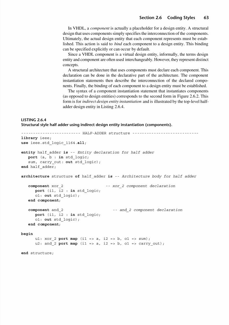
8/9/2019 VHDL for Engineers - Kenneth L. Short.pdf
http://slidepdf.com/reader/full/vhdl-for-engineers-kenneth-l-shortpdf 96/719
Section 2.6 Coding Styles 63
In VHDL, a component is actually a placeholder for a design entity. A structuraldesign that uses components simply specifies the interconnection of the components.Ultimately, the actual design entity that each component represents must be estab-lished. This action is said to bind each component to a design entity. This bindingcan be specified explicitly or can occur by default.
Since a VHDL component is a virtual design entity, informally, the terms designentity and component are often used interchangeably. However, they represent distinctconcepts.
A structural architecture that uses components must declare each component. Thisdeclaration can be done in the declarative part of the architecture. The componentinstantiation statements then describe the interconnection of the declared compo-nents. Finally, the binding of each component to a design entity must be established.
The syntax of a component instantiation statement that instantiates components(as opposed to design entities) corresponds to the second form in Figure 2.6.2. Thisform is for indirect design entity instantiation and is illustrated by the top-level half-adder design entity in Listing 2.6.4.
LISTING 2.6.4Structural style half adder using indirect design entity instantiation (components).
------------------------- HALF-ADDER structure ----------------------------library ieee;use ieee.std_logic_1164.all;
entity half_adder is -- Entity declaration for half adder port (a, b : in std_logic; sum, carry_out: out std_logic);end half_adder;
architecture structure of half_adder is -- Architecture body for half adder
component xor_2 -- xor_2 component declaration port (i1, i2 : in std_logic; o1: out std_logic); end component;
component and_2 -- and_2 component declaration port (i1, i2 : in std_logic;
o1: out std_logic); end component;
begin
u1: xor_2 port map (i1 => a, i2 => b, o1 => sum); u2: and_2 port map (i1 => a, i2 => b, o1 => carry_out);
end structure;

8/9/2019 VHDL for Engineers - Kenneth L. Short.pdf
http://slidepdf.com/reader/full/vhdl-for-engineers-kenneth-l-shortpdf 97/719
64 Chapter 2 Entities, Architectures, and Coding Styles
ComponentDeclarations
As previously stated, when components are used, each must be declared. A componentdeclaration is similar to an entity declaration in that it provides a listing of the compo-nent’s name and its ports.
Component declarations start with the keyword component. In the declarativepart of the half_adder architecture in Listing 2.6.4, componentsxor_2 and and_2
are declared. The component declaration for the XOR gate is:
component xor_2 port (i1, i2 : in std_logic; o1: out std_logic);end component;
ComponentDeclaration Syntax
A component declaration has the simplified syntax shown in Figure 2.6.4.
Component
Instantiation
The first component instantiation in Listing 2.6.4, with label u1, specifies an
instance of an xor_2 component:
u1: xor_2 port map (i1 => a, i2 => b, o1 => sum);
The xor_2 component in this instantiation statement must be bound to a designentity. To take full advantage of the power and flexibility of components, thisbinding could be specified explicitly, using a configuration declaration. Configu-ration declarations are discussed in detail in Chapter 15. However, for simple situa-tions a default configuration is used.
Default
Configuration Rules
In Listing 2.6.4, we take advantage of VHDL’s default configuration rules. Theserules implicitly bind a component to a design entity having the same name and sameport interface. Port interfaces are the same if the ports have identical names and types.
Since direct instantiation of design entities is more concise, it is used extensivelyin examples in this book until Chapter 15. In Chapter 15 we examine components ingreater detail and explore situations in which their use is advantageous.
component_declaration ::=
component identifier [is]
[port ( local_port _interface_list);]
end component [component_simple_name] ;
local_port _interface_list ::=
[signal] identifier_list : [ mode ] subtype_indication [ := static _expression ]
{; [signal] identifier_list : [ mode ] subtype_indication [ := static _expression ] }
FIGURE 2.6.4
Simplified syntax for a component declaration.

8/9/2019 VHDL for Engineers - Kenneth L. Short.pdf
http://slidepdf.com/reader/full/vhdl-for-engineers-kenneth-l-shortpdf 98/719
Section 2.6 Coding Styles 65
Mixed Style There is no restriction against using different kinds of concurrent statements in thesame architecture body. Doing so results in a mixed style. In fact, most designs use amixed coding style.
A mixed style half adder is given in Listing 2.6.5. Output sum is described using adataflow concurrent statement. Output carry_out is described using a process con-
current statement labeled co.
Behavior versusStructure
In describing architectural coding styles, we have made a distinction between dataflowand behavioral styles. Both of these styles actually describe behavior. Examination of either of these two kinds of descriptions tells us the behavior of the design entity. In thedataflow style, behavior is described indirectly by concurrent signal assignment state-ments, from which the corresponding behavior can be inferred. In the behavioral style,behavior is described algorithmically using process statements.
We will see later that a concurrent signal assignment statement used in dataflowstyle architecture is easily converted to an equivalent process statement that can be
used in a behavioral style architecture. In fact, a concurrent signal assignmentstatement is simply a shorthand representation of a process.
LISTING 2.6.5Mixed style half-adder description.
library ieee;use ieee.std_logic_1164.all;
entity half_adder is
port (a, b : in std_logic; sum, carry_out: out std_logic); end half_adder;
architecture mixed of half_adder is
begin
sum <= a xor b; -- dataflow concurrent statement
co: process (a,b) -- start of process concurrent statement begin
if a = '1' then
carry_out <= b; else
carry_out <= '0'; end if; end process co; -- end of process concurrent statement
end mixed;

8/9/2019 VHDL for Engineers - Kenneth L. Short.pdf
http://slidepdf.com/reader/full/vhdl-for-engineers-kenneth-l-shortpdf 99/719
66 Chapter 2 Entities, Architectures, and Coding Styles
In contrast, in a structural style description the top-level entity simply describes theinterconnection of components; it provides no behavioral information. Ultimately, thelowest level components in a structural design must each be described behaviorally intheir respective architectures. Otherwise, the top-level description cannot be compiled,simulated, or synthesized.
2 .7 S YN TH ES IS RE SU LT S VE RS US CO DI NG ST YL E
When the same system is described using different coding styles, but synthesized tothe same target PLD, we might expect that the resulting synthesized logic at the gatelevel is identical. This is usually the case for simple designs. However, for complexdesigns, the gate level logic, while functionally equivalent, may not be identical.This can occur because when starting from different functionally equivalent descrip-tions of the same system, the synthesizer optimization processes may not produce
the same gate level results. Still, the results are functionally equivalent.
DiagramsRepresentingSynthesized Logic
Some synthesizers provide a RTL hierarchical view of the synthesized logic as well asa technology dependent flattened to gates view. The RTL level hierarchical view iswhat results from step 1 of the synthesis process (see page 29) and depends on the styleof the description. However, it is the technology dependent flattened to gates view (fromsynthesis step 3) of different descriptions of the same system that are likely to be thesame. Our half-adder descriptions are simple enough that this is the case.
Half-AdderDataflow
DescriptionHierarchicalRepresentation
The RTL hierarchical representation of the hardware synthesized from the dataflowstyle half-adder description in Listing 2.6.1 is shown in Figure 2.7.1. As we might
have expected, an AND gate and an XOR gate are shown.
FIGURE 2.7.1
RTL hierarchical view of synthesized logic from the dataflow style description ofa half adder.
carry_out
carry_out
sum
sum
b
a

8/9/2019 VHDL for Engineers - Kenneth L. Short.pdf
http://slidepdf.com/reader/full/vhdl-for-engineers-kenneth-l-shortpdf 100/719
Section 2.7 Synthesis Results versus Coding Style 67
Half-AdderBehavioralDescriptionHierarchicalRepresentation
The RTL hierarchical representation of the hardware synthesized from the behav-ioral style half-adder description in Listing 2.6.2 is given in Figure 2.7.2. Perhapsunexpectedly, this representation shows two 2-input multiplexers.
The if statement from Listing 2.6.2 is initially synthesized as two multiplexers.The correlation between the code and the synthesized logic is straightforward. Inputa is the select input to both multiplexers. If a = '1', the bottom multiplexer routesthe complement of b to its output sum and the top multiplexer routes b to its outputcarry_out.
The if statement’s else branch corresponds to the situation where a = '0'. For this
condition, the bottom multiplexer routes b to sum and the top multiplexer routes '0'to carry_out.
Half-AdderStructuralDescriptionHierarchicalRepresentation
The RTL hierarchical representation of the hardware synthesized from the structuralstyle half-adder description in Listing 2.6.3 is given in Figure 2.7.3. The two componentinstantiation statements cause two design entities to be instantiated. These designentities are represented as rectangles, each labeled with the design entity’s name. It isonly because descriptive names were chosen for the instantiated design entities that wemight infer their functions. Distinctive shape logic symbols are not used because in astructural style design what is being represented is the interconnection of design
entities, not their functions.
TechnologyDependentFlattened toGates View
When the synthesis process is completed for the half-adder description written ineach style, the results are all the same, as shown in Figure 1.9.3, which is repeatedhere as Figure 2.7.4. This is the final technology dependent flattened to gates view.In addition to the logic gates, this representation shows buffers associated with theinput and output pins of the target PLD.
FIGURE 2.7.2
RTL hierarchical view of synthesized logic from the behavioral style descriptionof a half adder.
a
b
carry_out
carry_out
sum
sum
00
1
0
1

8/9/2019 VHDL for Engineers - Kenneth L. Short.pdf
http://slidepdf.com/reader/full/vhdl-for-engineers-kenneth-l-shortpdf 101/719
68 Chapter 2 Entities, Architectures, and Coding Styles
SynthesisConstraints
Another way of synthesizing functionally equivalent logic that differs at the gate levelis through the use of synthesis constraints. Synthesis constraints are design goals thatwe can specify for a synthesizer’s optimizer to try to achieve. These constraints arenot part of the VHDL language and are only discussed here in general terms.
Different synthesis constraints may cause different optimized circuits to besynthesized from the same architecture. All the optimized circuits are functionallyidentical.
Area Constraints The most common synthesis constraints are for area and speed. Area constraints
limit the area of the circuit in terms of the number of target technology primitives
used. Area is often expressed in terms of the number of equivalent gates.
TimingConstraints
Timing constraints are expressed in terms of when signals arrive at the circuit’s inputsand when they need to arrive at the circuit’s outputs. Sometimes the implementationwith the smallest area is also the fastest. Yet, these two goals often represent a trade-off,
FIGURE 2.7.3
RTL hierarchical view of synthesized logic from the structural style descriptionof a half adder.
b
acarry_out
sum
and_2
u2
i1i2
o1
xor_2
u1
i1
i2 o1
FIGURE 2.7.4
Technology dependent flattened-to-gates representation of synthesized halfadder.
a
b
sum
carry_out
a.O
b.O
sum.O
carry_out.O
G_4.O
carry_out_0_and2.O
8/9/2019 VHDL for Engineers - Kenneth L. Short.pdf
http://slidepdf.com/reader/full/vhdl-for-engineers-kenneth-l-shortpdf 102/719
Section 2.8 Levels of Abstraction and Synthesis 69
with timing being minimized by carrying out logic operations in parallel, thus increasingthe area.
Some synthesizers allow us to specify constraints in a graphical user interface.Others use command lines or a separate constraint file. VHDL’s user attribute featureeven allows constraints to be specified in the design description. However, this latter
approach may limit a design description’s portability.
2 .8 L EV EL S O F A BS TR AC TI ON AN D S YN TH ES IS
The level of abstraction used in describing a system refers to the amount of imple-mentation or structural detail in a description. Behavior refers to the function of anintended system independent of the level of abstraction used in its description. Useof a high level of abstraction allows us to describe a complex system’s behaviorwithout being overwhelmed by the large amount of detail and complexity required to
describe the system at the gate level.Table 2.8.1 is a listing of hierarchically related levels of abstraction for a system,
from most abstract at the top to least abstract (most detailed) at the bottom. This charac-terization also indicates the “components” used to represent the system at each level.
The levels of abstraction in Table 2.8.1 are commonly used in traditional designmethodologies to describe or model a design. In a traditional top-down design method-ology, a design is conceived at the behavioral level. The design is then developed as astepwise refinement from one level of abstraction to the next lower level. When eitherthe gate or transistor level is reached, depending on the technology to be used forimplementation, all the detail necessary to implement the design is available.
Table 2.8.1Levels of abstraction.
Level Components Representation
Behavioral Algorithms, FSMs Algorithmic representation ofsystem functions
System(architectural)
Processors, memories,functional subsystems
Interconnection of majorfunctional units
Register Transfer(dataflow)
Registers, adders,comparators, ALUs,counters, controllers, bus
Data movement andtransformation and requiredsequential control
Gate(logic level)
Gates, flip-flops Implementation of register levelcomponents using gates and flip-flops
Transistor Transistors, resistors,capacitors
Implementation of gates andflip-flops using transistors, capacitors, and resistors

8/9/2019 VHDL for Engineers - Kenneth L. Short.pdf
http://slidepdf.com/reader/full/vhdl-for-engineers-kenneth-l-shortpdf 103/719
70 Chapter 2 Entities, Architectures, and Coding Styles
Using VHDL, we can describe a system at any level of abstraction. We can describea system at the highest level of abstraction in a purely behavioral or algorithmicfashion, without any consideration of its structure or logic implementation. Such adescription represents the system as a black box describing its behavior as a function of its input values over time.
Alternatively, we can describe a system structurally at a high level of abstractionas an interconnection of subsystems, without any detail concerning each subsystem’sbehavior. In contrast, we can also describe a system structurally at (what is for ourpurposes) its most detailed level, gate level.
RTL Synthesizersversus BehavioralSynthesizers
Given a natural language behavioral specification for a simple system, we can writea corresponding high-level VHDL behavioral style description of the system. As wehave seen with the half-adder example, a properly written behavioral description of asimple system can be directly synthesized.
Given a natural language behavioral specification for a complex system, we can
also write a corresponding high-level VHDL behavioral style description. We maynot be able to directly synthesize this description. This is particularly true for adescription that involves complex algorithms. However, this description can be usedto verify the desired functionality.
For synthesis in this latter situation, we may have to translate the high-levelbehavioral description into a high-level structural description of an architecture thatcan implement the algorithm. For complex arithmetic designs, issues such as sched-uling, hardware allocation, resource sharing, and memory inferencing are a part of creating such an optimal architecture.
Register TransferLevel Synthesizers
In our VHDL/PLD design methodology, translation of a high-level behavioraldescription involving complex algorithms to a high-level structural description isdone manually. The resulting structural description is called a register transfer level(RTL) description. A properly written RTL VHDL description can be directlysynthesized to gate-level logic by a RTL VHDL synthesizer. The vast majority of VHDL synthesizers are RTL synthesizers. The designs in this book are all synthe-sizable by a RTL VHDL synthesizer. IEEE Std 1076.6 is for RTL VHDL synthe-sizers.
BehavioralSynthesizers
For complex behavioral descriptions, a relatively new type of synthesizer called abehavioral synthesizer is available. A behavioral synthesizer can often translate acomplex behavioral VHDL description to a RTL description and from there to a gate-level implementation. Behavioral synthesis has advantages for implementation of complex algorithmic systems. However, behavioral synthesizers are expensive andtheir use is beyond the scope of this book.

8/9/2019 VHDL for Engineers - Kenneth L. Short.pdf
http://slidepdf.com/reader/full/vhdl-for-engineers-kenneth-l-shortpdf 104/719
Section 2.9 Design Hierarchy and Structural Style 71
2 . 9 D E S IG N H I E R ARC H YA N D S T R U C T U R A L S T Y L E
As seen in the half-adder example in Section 2.6, use of structural style is relatively
inefficient when describing a system at the gate level. The advantages of structuralstyle become more evident as the complexity of the components used increases,requiring that the system be designed in a hierarchical fashion.
Hierarchical Design The hierarchical design of a complex system begins with a top-down successivedecomposition of the system’s specification into specifications for simpler componentdesign entities. Each design entity at a given level may be further decomposed intoconstituent design entities that comprise the next lower level of the decomposition.Eventually, a point is reached where each design entity is simple enough to be behav-iorally described in VHDL.
Each design entity is individually coded and then verified using a specificallywritten testbench. The complete system is then implemented from the bottom up byinterconnecting its constituent design entities. This approach describes and synthe-sizes a complex system as a hierarchy of design entities. Finally, a testbench iswritten to verify the complete system.
A particular design entity can be instantiated (used) multiple times in an archi-tecture, in the same way that multiple instances of the same IC component are usedin traditional hardware design.
Top-Level DesignEntity
The design entity that represents the entire system is the top-level design entity. The
architecture of the top-level design entity defines the system in terms of the intercon-nection of component design entities.Component design entities are interconnected by signals. Signals are analogous to
wires or printed circuit board traces in a corresponding hardware implementation.
External and LocalSignals
From the viewpoint of the top-level design entity, signals are divided into two kinds:external and local. External signals are accessed from outside the top-level designentity. External signals allow input to and output from the top-level design entity.Such signals are port signals (or simply ports).
Component design entities are interconnected by local (internal) signals to formthe top-level design entity. A local signal cannot be accessed from outside of itsenclosing architecture body. Local signals are simply referred to as signals.
Full-AdderStructuralDescription
A simple example of hierarchical design using structural style is given here for a fulladder. Hierarchical design is discussed in detail in Chapter 15.
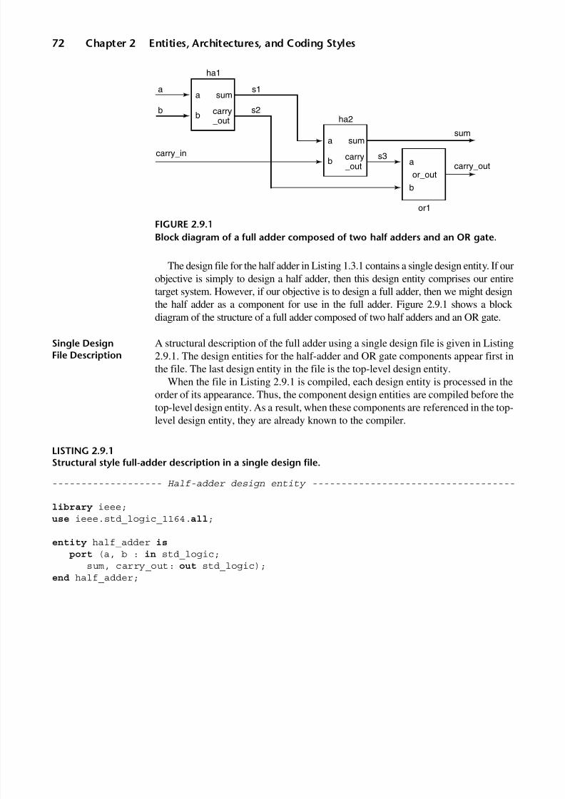
8/9/2019 VHDL for Engineers - Kenneth L. Short.pdf
http://slidepdf.com/reader/full/vhdl-for-engineers-kenneth-l-shortpdf 105/719
72 Chapter 2 Entities, Architectures, and Coding Styles
The design file for the half adder in Listing 1.3.1 contains a single design entity. If ourobjective is simply to design a half adder, then this design entity comprises our entiretarget system. However, if our objective is to design a full adder, then we might designthe half adder as a component for use in the full adder. Figure 2.9.1 shows a block diagram of the structure of a full adder composed of two half adders and an OR gate.
Single DesignFile Description
A structural description of the full adder using a single design file is given in Listing2.9.1. The design entities for the half-adder and OR gate components appear first inthe file. The last design entity in the file is the top-level design entity.
When the file in Listing 2.9.1 is compiled, each design entity is processed in theorder of its appearance. Thus, the component design entities are compiled before the
top-level design entity. As a result, when these components are referenced in the top-level design entity, they are already known to the compiler.
LISTING 2.9.1Structural style full-adder description in a single design file.
------------------- Half-adder design entity -----------------------------------
library ieee;use ieee.std_logic_1164.all;
entity half_adder is
port (a, b : in std_logic; sum, carry_out: out std_logic);end half_adder;
FIGURE 2.9.1
Block diagram of a full adder composed of two half adders and an OR gate.
ha1
or1
a
b
a
b
s1
s2
sum
carry_out ha2
a
b
sum
carry_out
a
b
or_out
carry_in
sum
carry_outs3

8/9/2019 VHDL for Engineers - Kenneth L. Short.pdf
http://slidepdf.com/reader/full/vhdl-for-engineers-kenneth-l-shortpdf 106/719
Section 2.9 Design Hierarchy and Structural Style 73
architecture dataflow of half_adder is
begin
sum <= a xor b; carry_out <= a and b;end dataflow;
------------------- Two input OR gate design entity ----------------------------
library ieee;use ieee.std_logic_1164.all;
entity or_2 is
port (a, b : in std_logic; or_out : out std_logic);end or_2;
architecture dataflow of or_2 is
begin or_out <= a or b;end dataflow;
------------------- Full-adder design entity -----------------------------------
library ieee;use ieee.std_logic_1164.all;
entity full_adder is
port (a, b, carry_in : in std_logic; sum, carry_out: out std_logic);end full_adder;
architecture structure of full_adder is
signal s1, s2, s3 : std_logic; -- Signals to interconnect components
begin
-- Each component instantion below is a concurrent statement
ha1: entity half_adder port map (a => a, b => b, sum =>s1, carry_out => s2); ha2: entity half_adder port map (a => s1, b => carry_in, sum => sum,
carry_out => s3); or1: entity or_2 port map (a => s3, b => s2, or_out => carry_out);
end structure;

8/9/2019 VHDL for Engineers - Kenneth L. Short.pdf
http://slidepdf.com/reader/full/vhdl-for-engineers-kenneth-l-shortpdf 107/719
74 Chapter 2 Entities, Architectures, and Coding Styles
Declaring (Local)Signals
Signals s1, s2, and s3, needed to connect the design entities, are declared in thedeclarative part of the full-adder’s architecture for use in its statement part.
In the architecture’s statement part there are three component instantiation state-ments. Each describes an instance of a design entity and how it is interconnected inthe larger structure. The half-adder design entity is instantiated twice. Signals s1,
s2, and s3 are used in the port maps to interconnect the design entities.
Multiple DesignFile Description
The same structural full-adder design can be described using three separate files,each containing only one design entity. The text in the separate files for the half adder and the OR gate would be the same as for their respective design entities inListing 2.9.1.
The separate design file for the top-level design entity appears in Listing 2.9.2.This file assumes that the half-adder and OR gate design entities have been compiledto a user-created library called parts. The second library statement makes compo-nents in the library parts available. Otherwise, the description of the top-level
design entity is the same as in the single design file version.
LISTING 2.9.2Design file containing top-level design entity for a multiple design file full adder.
------------------- Full-adder design entity -----------------------------------
library ieee;use ieee.std_logic_1164.all;library parts;use parts.all;
entity full_adder is
port (a, b, carry_in : in std_logic; sum, carry_out: out std_logic);end full_adder;
architecture structure of full_adder is
signal s1, s2, s3 : std_logic; -- Signals to interconnect components
begin
ha1: entity half_adder port map (a => a, b => b, sum => s1, carry_out => s2); ha2: entity half_adder port map (a => s1, b => carry_in, sum => sum, carry_out => s3); or1: entity or_2 port map (a => s2, b => s3, or_out => carry_out);
end structure;

8/9/2019 VHDL for Engineers - Kenneth L. Short.pdf
http://slidepdf.com/reader/full/vhdl-for-engineers-kenneth-l-shortpdf 108/719
Problems 75
For a complex design, having each design entity in a separate file allows us todesign and verify each one separately. This simplifies design management, allowingus to focus on one thing at a time. As a further step, placing design entities into alibrary also allows us to easily reuse them in other designs.
PROBLE MS
2.1 What is a design unit?
2.2 List the five kinds of library units.
2.3 Why is a design entity separated into an entity declaration and an architecture body?
2.4 What information does an entity declaration provide about a design entity?
2.5 Explain the meanings of the following symbols when used in syntax definitions: ::=, |, [ ],and { }.
2.6 What does it mean for an IEEE Std 1076.6 compliant synthesizer to accept a construct? Whatdoes it mean for an IEEE Std 1076.6 synthesizer to interpret a construct?
2.7 What are the meanings of the terms supported, ignored, and not supported in the context of classifying VHDL constructs for an IEEE Std 1076.6 compliant synthesizer? How are parts of a construct that are ignored by an IEEE Std 1076.6 compliant synthesizer indicated in a syntaxdefinition? How are parts of a construct that are not supported indicated?
2.8 Which of the following can be used as a valid identifier in a VHDL program and which cannot?For those that cannot, explain why.
(a) adder(b) result_(c) units(d) 4_to_1_mux(e) top_level(f) port
2.9 For each port mode, list the mode and the possible direction(s) of information transfer. Specifythese directions as in, out, or in and out. Which port mode is not acceptable for synthesis?
2.10 What is a signal source and what are the different kinds of signal sources?
2.11 In terms of their mode, which ports can be written by a signal assignment statement in anarchitecture body? Which ports can be read by a signal assignment in an architecture body?
2.12 In each of the following concurrent signal assignment statements, indicate which signals arewritten, which are read, and to which signals each statement is sensitive.
(a) f <= a and b and c;(b) g <= not (w and x and y);(c) eq <=(not x and not y) or (x and y);(d) eq <= (x_bar and y_bar) or (x and y);(e) alarm <= armed and (d1 or d2 or d3) or panic;

8/9/2019 VHDL for Engineers - Kenneth L. Short.pdf
http://slidepdf.com/reader/full/vhdl-for-engineers-kenneth-l-shortpdf 109/719
76 Chapter 2 Entities, Architectures, and Coding Styles
2.13 Given the following architecture body, write the associated entity declaration:
architecture csa of and_or is signal s1, s2 : std_logic ;begin s1 <= a and b; s2 <= a and c; f <= s1 or s2;end csa;
2.14 What is the difference in operation of a port of mode inout and one of mode buffer?
2.15 What information about a design entity does an architecture body provide?
2.16 Into what two parts is an architecture body divided? What is the purpose of each part?
2.17 What are the three different pure coding styles for an architecture body and how is eachdistinguished?
2.18 A two-to-one multiplexer has two data inputs, a and b, and one select control input, s. Themultiplexer has a single output c. If s = 0, c is equal to a. If s = 1, c is equal to b.
(a) Write an entity declaration for the multiplexer named mux. Use only the data typestd_logic.
(b) Write an architecture for mux that uses Boolean equations in a dataflow style architecture.(c) What other statements must be included in the design file containing the multiplexer’s
entity and architecture in order to compile the design entity? Why must these statementsbe included?
2.19 Given the following truth table:
(a) Write a canonical sum-of-products Boolean equation for each output.(b) Write a complete VHDL design description of a design entity that accomplishes the
function defined by the truth table. Use a simple dataflow architecture where the signalassignment statements are Boolean equations.
a b c x y
0 0 0 0 1
0 0 1 1 0
0 1 0 1 0
0 1 1 0 0
1 0 0 1 0
1 0 1 0 1
1 1 0 0 1
1 1 1 1 0

8/9/2019 VHDL for Engineers - Kenneth L. Short.pdf
http://slidepdf.com/reader/full/vhdl-for-engineers-kenneth-l-shortpdf 110/719
Problems 77
2.20 Write a design description that accomplishes the function defined by the following truth table.Use a dataflow style architecture consisting of Boolean equations.
2.21 A 74HC10 IC contains three 3-input NAND gates.
(a) Write an entity declaration for the design entitytriple_3 that is functionally equivalent
to a 74HC10.(b) Write an architecture in the dataflow style for the design entitytriple_3. Use only
signal assignment statements with Boolean equations.
2.22 What is a component in VHDL?
2.23 What does binding mean in terms of components and design entities? What is the defaultbinding rule for components?
2.24 Using only the design entities that follow, write the top_level design entity to complete thedescription of a circuit that is functionally equivalent to the Boolean equation:
Use direct design entity instantiation.
------------------------ OR gate component -------------------------library ieee; -- Load the IEEE 1164 libraryuse ieee.std_logic_1164.all; -- Make package visible to the next entity
entity or_2 is -- Entity declaration for 2 input or port (i1, i2 : in std_logic; o1: out std_logic);end or_2;
architecture dataflow of or_2 is -- Architecture body for 2 input or
begin o1 <= i1 or i2;end dataflow;
(Cont.)
a b c x y
0 0 0 0 1
0 0 1 1 0
0 1 0 0 1
0 1 1 0 0
1 0 0 1 0
1 0 1 0 0
1 1 0 0 0
1 1 1 0 1
y abc c+=

8/9/2019 VHDL for Engineers - Kenneth L. Short.pdf
http://slidepdf.com/reader/full/vhdl-for-engineers-kenneth-l-shortpdf 111/719
78 Chapter 2 Entities, Architectures, and Coding Styles
(Cont.)
------------------------- AND gate component --------------------------library ieee; -- Load the IEEE 1164 libraryuse ieee.std_logic_1164.all; -- Make package visible to the next entity
entity and_2 is -- Entity declaration for 2 input and port (i1, i2 : in std_logic; o1: out std_logic);end and_2;
architecture dataflow of and_2 is -- Architecture body for 2 input andbegin o1 <= i1 and i2;end dataflow;
------------------------- NOT gate component --------------------------
library ieee;-- Load the IEEE 1164 libraryuse ieee.std_logic_1164.all; -- Make package visible to the next entity
entity not_1 is -- Entity declaration for 2 input and port (i1 : in std_logic; o1: out std_logic);end not_1;
architecture dataflow of not_1 is -- Architecture body for 2 input andbegin o1 <= not i1;
end dataflow;
------------------------- TOPLEVEL structure ----------------------------- put your top-level design unit here
2.25 Given the following entity declaration and architecture body:
entity nand_2 is port (i1, i2 : in std_logic; o : out std_logic);end nand_2;
architecture dataflow of nand_2 is begin o <= i1 nand i2;end dataflow;

8/9/2019 VHDL for Engineers - Kenneth L. Short.pdf
http://slidepdf.com/reader/full/vhdl-for-engineers-kenneth-l-shortpdf 112/719
Problems 79
Write a design description of a two-input OR gate design entity that has inputs a and b andoutput c. Use a structural architecture consisting of only nand_2 components.
2.26 The figure below gives the pin assignments and logic diagram of a Fairchild NC7SP19 1-of-2Decoder/Demultiplexer IC.
(a) Write an entity declaration named nc7sp19 for an equivalent function. Label the inputsand outputs to correspond as closely as possible to the names used in the diagram. Powerand ground pins are not included as ports in entity declarations. Also, ignore the pinnumbers.
(b) Write a complete design file for the entitync7sp19 that includes a top-level structuraldescription. Use the OR gate component or_2 and the inverter component not_1 fromProblem 2.24. Label the components in the diagram u1 to u3 from top to bottom. Usedirect design entity instantiation in the top-level structural architecture. Use namedassociation in the port map.
2.27 As a hot-shot VHDL designer, you have been hired by Chapter 11 Electronics to salvage
their biggest project, which is in trouble because their chief engineer left the company. Allthat remains is a logic diagram covered with coffee stains and a partially completed VHDLdesign file. The partially completed file is the same as that given in Problem 2.24. To savethe company, you must finish the design by writing the description of the top-level designentity!
GND
A
2
1
3
5
6
4
VCC
Y0
Y1E
a
b
u3
u4
u5 c
s1
s2
s3
s4
u1
u2

8/9/2019 VHDL for Engineers - Kenneth L. Short.pdf
http://slidepdf.com/reader/full/vhdl-for-engineers-kenneth-l-shortpdf 113/719
80 Chapter 2 Entities, Architectures, and Coding Styles
2.28 For the logic diagram shown below:
Write a complete structural style design description consisting of a single design file. Thisdescription should correspond as closely as possible to the diagram. Use direct design entityinstantiation. Also, use named association in the port maps.
2.29 For the logic diagram shown below:
(a) Write a complete structural style design description consisting of a single source file.Name the architecture structural. This description should have a one-to-onecorrespondence with the diagram. Use direct instantiation. Also use only namedassociation in port maps.
(b) Write an alternative structural architecture for part (a) that uses indirect instantiation
(components).(c) Write a complete dataflow style design that uses a single concurrent signal assignment
consisting of a Boolean expression that uses only NAND operators.
2.30 For the design description that follows, draw the corresponding logic diagram.
library ieee;use ieee.std_logic_1164.all;
entity gate_ckt is port (a, b, c : in std_logic; f: out std_logic);end gate_ckt;
architecture structure of gate_ckt is signal s1, s2: std_logic; begin u0 : entity nand_2 port map (i1 => a, i2 => b, o1 => s1); u1 : entity nand_2 port map (i1 => s1, i2 => s2, o1 => f); u2 : entity invert port map (i1 => c, o1 => s2)end structure;
u1
u2
u3
a
bu0
c
f
a
b
/c f
u1
u2

8/9/2019 VHDL for Engineers - Kenneth L. Short.pdf
http://slidepdf.com/reader/full/vhdl-for-engineers-kenneth-l-shortpdf 114/719
Problems 81
Assume that the nand_2 entity is a two-input NAND gate and the invert entity is a NOTgate. Port names starting with an i indicate inputs and port names starting with an o indicateoutputs.
2.31 Of the three typical steps carried out by a logic synthesizer (see page 29) to the result of whichstep does the RTL hierarchical view of the synthesized logic correspond? To the result of which
synthesis step does the technology dependent flattened-to-gates view correspond?2.32 For descriptions of the same system written in different coding styles and synthesized for the
same target PLD, under what conditions would we expect the gate-level synthesized logic to beidentical? Under what conditions would we expect the gate-level synthesized logic to not beidentical? Should the gate-level synthesized logic be functionally the same under all conditions?
2.33 Why is the RTL hierarchical view of the logic synthesized for a design described in structuralstyle always represented as an interconnection of rectangular blocks?
2.34 What does “level of abstraction” mean in terms of the description of a system?
2.35 What is the advantage of using a description with a high level of abstraction when describinga complex system?
8/9/2019 VHDL for Engineers - Kenneth L. Short.pdf
http://slidepdf.com/reader/full/vhdl-for-engineers-kenneth-l-shortpdf 115/719
82
Chapter 3
Signals and Data Types
In digital systems, the logic signals that transfer information from one component toanother, and from one system to another, are voltages that vary in a discrete fashionwith respect to time and are carried by wires. In VHDL, signals play a similar andequally important role. Local signals connect components within an architecture toform a larger system. Port signals provide a system’s interface to its environment.
All signals in VHDL have a declared type. A signal’s type determines the set of values it can take and the operations that can be performed on those values.
Every signal must be declared before it is used. Where a signal is declared deter-mines where in the source code text it can be used—its scope or visibility. A signalcan only be referenced by statements that appear within the scope of its declaration.
Constants are also introduced in this chapter. A constant is a named object that isassigned a value when it is declared. Once a constant is assigned a value, its valuecannot be changed. Use of constants make a description more readable and easier tomodify.
3 .1 O BJ EC T C LA SS ES A ND O BJ EC T TY PE S
Signals belong to a class of VHDL language elements called objects. An object is anamed item that has a value of a specified type. To place the study of signals andconstants in context, this section presents an overview of objects and types.
Object Classes An object’s class represents the nature of the object and how it is used, for example,whether the object’s value can be modified and whether it has a time element

8/9/2019 VHDL for Engineers - Kenneth L. Short.pdf
http://slidepdf.com/reader/full/vhdl-for-engineers-kenneth-l-shortpdf 116/719
Section 3.1 Object Classes and Object Types 83
associated with it. Conventional programming languages typically have three classesof objects: constants, variables, and files. In contrast, VHDL has four:
• Signal: an object with a current value and projected (future) values. Theprojected values can be changed, as many times as desired, using signalassignment statements.
• Constant: an object whose value cannot be changed after it is initiallyspecified.
• Variable: an object with only a current value. A variable’s value can bechanged, as many times as desired, using variable assignment statements.
• File: an object that consists of a sequence of values of a specified type.
Signals, constants, and variables are synthesizable and are used in design descrip-tions. Files are not synthesizable; they are used mostly in testbenches.
Object Types Each VHDL object must be of some type. An object’s type defines the set of values
the object can assume and the set of operations that can be performed on thosevalues.
There are five types:
• Scalar type: has a single indivisible value, which can be either numeric orenumerated.
• Composite type: consists of a collection of elements each with a value. Thereare two kinds of composite types: arrays and records. All elements in an arrayare of the same type. Elements in a record can be of different types.
• Access type: provides access to objects of a given type, similar to a pointer in
conventional programming languages.• File type: provides access to objects containing a sequence of values of a given
type (such as disk files). The value of a file type is the sequence of valuescontained in the host system file.
• Protected type: provides atomic and exclusive access to variables accessible tomultiple processes (global variables).
Only scalar and composite types are synthesizable.
Strong Typing VHDL is a strongly typed language with strictly enforced type rules. If we mixdifferent types in an expression or exceed a type’s range of values, the compiler orsimulator generates an error message. For example, the integer value 0, the realnumber 0.0, and the bit value '0' are not the same type, and, therefore, are not thesame. VHDL’s strong typing makes it easier for a compiler to detect errors.
ObjectDeclarations
All objects must be declared before being used. A declaration introduces the nameof an object, defines its type, and, optionally, assigns an initial value.

8/9/2019 VHDL for Engineers - Kenneth L. Short.pdf
http://slidepdf.com/reader/full/vhdl-for-engineers-kenneth-l-shortpdf 117/719
84 Chapter 3 Signals and Data Types
This chapter focuses on signal and constant objects of scalar and composite types.Neither signals nor constants are allowed to be of access type.
3 . 2 S I GN AL O BJ E C T S
As seen in Chapter 2, the ports of a design entity are signals. From the viewpoint of a design entity, its ports can be thought of as external signals, which are simplyreferred to as ports. Signals within a design entity can be thought of as local orinternal signals, which are simply referred to as signals.
Scope andVisibility
For each signal declared, VHDL language rules define a certain region of text, calledscope or namespace, where the signal’s name can be used. A signal is said to bevisible (accessible) within its scope. Outside of its scope, a signal is unknown. Anyattempt to use a signal outside of its scope causes a compilation error.
A signal’s scope is determined by where it is declared. A signal can be declared inthe declarative part of an entity declaration, the declarative part of an architecturebody, or in a package declaration.
Port Visibility A port’s name is visible in the entity declaration in which it is declared and in anyarchitecture bodies associated with that entity declaration. A component declarationin the declarative part of an architecture makes that component’s port signals visiblein that architecture.
Signal Visibility A signal declared in the declarative part of an architecture body can only be usedwithin that architecture; it is not visible outside of that architecture.
InformationHiding
Once a design entity’s functionality has been verified, the details of its internaloperation are not subsequently of concern to a user of the design entity. This isconsistent with the concept of information hiding. Therefore, it is appropriate that asignal declared in the declarative part of an architecture body not be visible outsideof that architecture.
Port Declarations
The term port is used to refer only to signals declared by port declarations. Ports aredeclared in the port clause of an entity declaration, as was shown in Figure 2.1.1,which is repeated here as Figure 3.2.1.
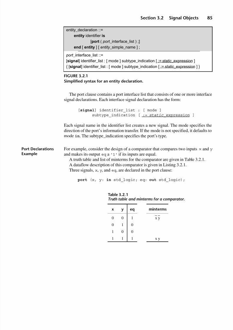
8/9/2019 VHDL for Engineers - Kenneth L. Short.pdf
http://slidepdf.com/reader/full/vhdl-for-engineers-kenneth-l-shortpdf 118/719
Section 3.2 Signal Objects 85
The port clause contains a port interface list that consists of one or more interfacesignal declarations. Each interface signal declaration has the form:
[signal] identifier_list : [ mode ] subtype_indication [ := static _expression ]
Each signal name in the identifier list creates a new signal. The mode specifies thedirection of the port’s information transfer. If the mode is not specified, it defaults tomode in. The subtype_indication specifies the port’s type.
Port DeclarationsExample
For example, consider the design of a comparator that compares two inputs x and y
and makes its output eq a '1' if its inputs are equal.A truth table and list of minterms for the comparator are given in Table 3.2.1.
A dataflow description of this comparator is given in Listing 3.2.1.Three signals, x, y, and eq, are declared in the port clause:
port (x, y: in std_logic; eq: out std_logic);
entity_declaration ::=
entity identifier is
[port ( port _interface_list ) ;]
end [ entity ] [ entity _simple_name ] ;
port _interface_list ::=[signal] identifier_list : [ mode ] subtype_indication [ := static _expression ]
{ [signal] identifier_list : [ mode ] subtype_indication [ := static _expression ] }
FIGURE 3.2.1
Simplified syntax for an entity declaration.
Table 3.2.1Truth table and minterms for a comparator.
x y eq minterms
0 0 1 x y
0 1 0
1 0 0
1 1 1 x y

8/9/2019 VHDL for Engineers - Kenneth L. Short.pdf
http://slidepdf.com/reader/full/vhdl-for-engineers-kenneth-l-shortpdf 119/719
86 Chapter 3 Signals and Data Types
LISTING 3.2.1Dataflow style comparator.
library ieee;use ieee.std_logic_1164.all;
entity compare is port (x, y: in std_logic; eq: out std_logic);end compare;
architecture dataflow of compare is
begin
eq <=(not x and not y) or (x and y);end dataflow;
A multiple object declaration, like the preceding, is equivalent to a sequence of the
corresponding number of single-object declarations. For example:
port (x: in std_logic; y: in std_logic; eq: out std_logic);
Single-object declarations are more readable, particularly when each is followed byan appropriate comment that states the purpose of the signal, but they require morespace.
For port declarations, the convention is to leave out the optional keywordsignal. So instead of writing:
signal x: in std_logic;
we simply write:
x: in std_logic;
Since x, y, and eq are declared in the port clause for compare, these signals arevisible (can be used) in any architecture associated with compare. Accordingly, thearchitecture dataflow of compare can (and does) use these port signals.
The architecture consists of a single concurrent signal assignment statement:
eq <=(not x and not y) or (x and y);
This is the canonical sum-of-products expression determined from the truth table inTable 3.2.1.

8/9/2019 VHDL for Engineers - Kenneth L. Short.pdf
http://slidepdf.com/reader/full/vhdl-for-engineers-kenneth-l-shortpdf 120/719
Section 3.2 Signal Objects 87
Signal Declarations
Signals are declared in the declarative part of an architecture using a signal decla-ration statement. The syntax for such a statement is given in Figure 3.2.2.
The syntax for a signal declaration looks just like that of an interface signal decla-ration, except that the keyword signal is required and no mode is specified. Unlikeports, signals do not have a mode. A signal can transfer information in eitherdirection.
:= Symbol The symbol used for assignment of an initial value to a signal in its declaration is :=.This is in contrast to the symbol <= used for signal assignment. Initial signal values
are useful for simulation, but not for synthesis. For synthesis, any initial or default
value assigned to a signal is ignored by an IEEE 1076.6 compliant synthesizer.
This is because the synthesizer cannot assume that the target hardware has thecapability to be powered up with its signals in the specified states.
Note that there are some synthesizers that attempt to synthesize initial values(with varying degrees of success). However, for a design description to be IEEE Std1076.6 compliant, initial values must not be assigned to signals or variables.
For purposes of simulation, in the absence of an explicit initial value expression,an implicit default value is assigned to a signal. This default value is equal to theleftmost value in the range of values for the specified type.
Using Signalsto ConnectConcurrentStatements
We have previously used signals in structural style architectures, where it was clearthat their purpose was to connect design entities, just as wires connect components inan electronic system. Signals are also used to connect concurrent signal assignmentstatements in dataflow style architectures and processes in behavioral style architec-
tures. In effect, signals allow concurrent statements of any kind to communicate witheach other.
ConnectingConcurrent SignalAssignmentStatements
The dataflow architecture for design entity compare in Listing 3.2.1 did not use anysignals. A second dataflow style architecture for compare is given in Listing 3.2.2.
Signals x_bar and y_bar are declared in the declarative part of architecturedataflow2. These signals are visible only within this architecture. This architectureis named dataflow2 to distinguish it from the previous architecture (dataflow)for the same entity declaration.
signal_declaration ::=
signal identifier_list : subtype_indication [:= static_ expression] ;
FIGURE 3.2.2
Simplified syntax for a signal declaration.

8/9/2019 VHDL for Engineers - Kenneth L. Short.pdf
http://slidepdf.com/reader/full/vhdl-for-engineers-kenneth-l-shortpdf 121/719
88 Chapter 3 Signals and Data Types
LISTING 3.2.2Dataflow style comparator using local signals.
library ieee;use ieee.std_logic_1164.all;
entity compare is port (x, y: in std_logic; eq: out std_logic);end compare;
architecture dataflow2 of compare is
signal x_bar, y_bar: std_logic;begin
x_bar <= not x; y_bar <= not y; eq <= (x_bar and y_bar) or (x and y);end dataflow2;
Use of signals x_bar and y_bar in Listing 3.2.2 demonstrates that signals canconnect concurrent signal assignment statements in an architecture. In a morecomplex dataflow architecture, it might be advantageous to break a single complexconcurrent signal assignment statement into multiple constituent statements toimprove readability.
3 . 3 SC A L AR TY P E S
The signals we have encountered in previous programs were all scalar types. Aspreviously stated, a scalar type represents a single indivisible value. Scalar types areclassified as either enumeration, integer, physical, or floating point (Figure 3.3.1).
Discrete Types andNumeric Types
Enumeration types and integer types are discrete types. Discrete types represent setsof distinct values. Integer types are also classified as numeric types, as are physicaltypes and floating point types. All numeric types can be specified with a range thatconstrains the set of possible values.
Type Declarations Just as all signals must be declared with a type before they are used, all types must alsobe declared before use. Types are declared using a type declaration (Figure 3.3.2). Thetype definition portion of a type declaration defines the set of values an object of thattype can have.

8/9/2019 VHDL for Engineers - Kenneth L. Short.pdf
http://slidepdf.com/reader/full/vhdl-for-engineers-kenneth-l-shortpdf 122/719
Section 3.3 Scalar Types 89
Types used for ports must be declared in a package, so that the type is visible toentity declarations. A package must be compiled before any entity declaration thatuses a type declared in that package is compiled.
Predefined Types Predefined (built-in) types are those defined in packages STANDARD and TEXTIOin the library STD. This library is provided with all VHDL compilers. PackageTEXTIO is provided to support formatted human-readable I/O.
FIGURE 3.3.1
Predefined scalar types.
Scalar Types
EnumerationTypes
IntegerTypes
integer
PhysicalTypes
time
FloatingTypes
real
discrete
numeric
p r e d e f i n e
d
bit
(chap. 3) (chap. 3) (chap. 7)
boolean
(chap. 4)
character
(chap. 3)
severity_level
(chap. 7)
file_open_kind
file_open_status
type_declaration ::=
type identifier is type_definition ;
FIGURE 3.3.2
Simplified syntax for a type declaration.

8/9/2019 VHDL for Engineers - Kenneth L. Short.pdf
http://slidepdf.com/reader/full/vhdl-for-engineers-kenneth-l-shortpdf 123/719
90 Chapter 3 Signals and Data Types
The predefined scalar types in Figure 3.3.1 are defined in package STANDARD.Of these, only bit, boolean, character, and integer are synthesizable. Types character,bit, and integer are discussed in this chapter. The other predefined scaler types arediscussed in later chapters.
To use a type that is declared in a package, we must precede each entity decla-ration that uses that type with an appropriate context clause. Because every designunit in a description is automatically preceded by the implicit context clause:
library std, work;use std.standard.all;
the predefined types in package STANDARD are directly visible in a design withoutexplicitly using any library or use clauses.
Enumeration Types An enumeration type is declared by simply listing (enumerating) all possible valuesfor the type. There must be at least one value in the list. The syntax for declaring anenumeration type is given in Figure 3.3.3.
Identifier is the name given to the type. The type definition portion of an enumer-ation type declaration consists of the list of enumeration literals (values) for the type.An enumeration literal can be an identifier or a character literal.
Like all other VHDL identifiers, an identifier used as an enumeration literal is notcase sensitive. In contrast, character literals are case sensitive. A character literal is asingle character enclosed in single quotes. For example, the single characters 'a'
and 'A' are distinct. An enumeration type is said to be a character type if at least oneof its enumeration literals is a character literal.
Each enumeration literal must be unique within the type being declared.However, different enumeration types may use the same literal. In such cases, theliteral is said to be overloaded.
All scalar types are ordered. All relational operators (>, <, =, and so on) arepredefined for their values. Enumeration literals are ordered, in ascending order, by
their textual position in the list of literals defining the type.
Type Character Type character is an enumeration type, predefined in package STANDARD, thatcorresponds to the International Organization for Standardization (ISO) 8-bitencoded character set ISO 8859-1:1987. This character set includes graphiccharacters and format effectors. The definition of type character contains a mixtureof character literals and identifiers as elements:
enumeration_type_declaration ::=
type identifier is ( enumeration_literal { , enumeraton_literal } )
enumeration_literal ::= identifier | character_literal
FIGURE 3.3.3
Simplified syntax for an enumeration type declaration.

8/9/2019 VHDL for Engineers - Kenneth L. Short.pdf
http://slidepdf.com/reader/full/vhdl-for-engineers-kenneth-l-shortpdf 124/719
Section 3.3 Scalar Types 91
type character is (NUL, SOH, STX, ETX, EOT, ENQ, ACK, BEL, BS, HT, LF, VT, FF, CR, SO, SI,
DLE, DC1, DC2, DC3, DC4, NAK, SYN, ETB,CAN, EM, SUB, ESC, FSP, GSP, RSP, USP,' ', '!', '"', '#', '$', '%', '&', ''','(', ')', '*', '+', ',', '-', '.', '/',
'0', '1', '2', '3', '4', '5', '6', '7', '8', '9', ':', ';', '<', '=', '>', '?', '@', 'A', 'B', 'C', 'D', 'E', 'F', 'G', 'H', 'I', 'J', 'K', 'L', 'M', 'N', 'O', 'P', 'Q', 'R', 'S', 'T', 'U', 'V', 'W', 'X', 'Y', 'Z', '[', '\', ']', '^', '_', '`', 'a', 'b', 'c', 'd', 'e', 'f', 'g', 'h', 'i', 'j', 'k', 'l', 'm', 'n', 'o', 'p', 'q', 'r', 's', 't', 'u', 'v', 'w', 'x', 'y', 'z', '{', '|', '}', '~', DEL, C128, C129, C130, C131, C132, C133, C134, C135,
C136, C137, C138, C139, C140, C141, C142, C143,C144, C145, C146, C147, C148, C149, C150, C151,C152, C153, C154, C155, C156, C157, C158, C159,
' ', '¡', '¢', '£', '‡', '¥', '¦', '§','¨', '©', 'ª', '«', '¬', '-', '®', '¯','°', '±', '²', '³', '´', 'µ', '¶', '·','¸', '¹', 'º', '»', '¼', '½', '¾', '¿','À', 'Á', 'Â', 'Ã', 'Ä', 'Å', 'Æ', 'Ç','È', 'É', 'Ê', 'Ë', 'Ì', 'Í', 'Î', 'Ï','Ð', 'Ñ', 'Ò', 'Ó', 'Ô', 'Õ', 'Ö', '×','Ø', 'Ù', 'Ú', 'Û', 'Ü', 'Ý', 'Þ', 'ß',
'à', 'á', 'â', 'ã', 'ä', 'å', 'æ', 'ç','è', 'é', 'ê', 'ë', 'ì', 'í', 'î', 'ï','ð', 'ñ', 'ò', 'ó', 'ô', 'õ', 'ö', '÷','ø', 'ù', 'ú', 'û', 'ü', 'ý', 'þ', 'ÿ');
The first 128 characters in this enumeration are the ASCII characters. The identifiersfrom NUL to USP and DLE are the nonprintable ASCII control characters. CharactersC128 toC159 in the ISO character set do not have names. In VHDL, these charactersare given names based on their positions in the enumeration.
The character in position 160 is the nonbreaking space character, in contrast to theordinary space character in position 32. The character at position 173 is the soft
hyphen, in contrast to the ordinary hyphen in position 45. The soft hyphen is used torepresent a line break within a word.
Type Bit Type bit is an enumeration type used as a simple representation for a logic signal.The type declaration for bit appears in package STANDARD as:
type bit is ('0','1');

8/9/2019 VHDL for Engineers - Kenneth L. Short.pdf
http://slidepdf.com/reader/full/vhdl-for-engineers-kenneth-l-shortpdf 125/719
92 Chapter 3 Signals and Data Types
Here character literals '0' and '1' are used to represent logic 0 and logic 1. Hence,type bit is also a character type. Because of their order in the enumeration list, '0' isless than '1'.
SubtypeDeclarations
A type derived from another type is a subtype. The type from which the subtype isderived is its base type. Creating and using a subtype allows us to make it clearwhich values from the base type are valid for an object.
The simplified syntax for a subtype declaration is given in Figure 3.3.4. From thesyntax, we see that a subtype is simply a type together with either a resolutionfunction or a constraint, or both.
Inclusionin a Subtype
A value belongs to a subtype of a given type if it belongs to the base type andsatisfies the constraint, if any, of the subtype declaration. A constraint is a restrictionon the set of possible values for the subtype from the values allowed for the base
type. A type is a subtype of itself. Such a subtype is unconstrained because it corre-sponds to a situation that imposes no restrictions. A subtype declaration does not define a new type. The type of a subtype is the
same as its base type. Accordingly, the set of operations allowed on a subtype is the
same as the set allowed on its base type.
An example of a subtype declaration using a resolution function is given in the nextsection. Examples of subtype declarations using constraints are given in Section 3.10.
Type Compatibilityin Assignments
When a signal assignment is made, the objects on both sides of the assignmentsymbol must be of the same type. Otherwise, the compiler gives a type conflict error.This ensures that an object is only assigned values of its own type and avoids mixing
values that represent different things.Since a subtype declaration does not define a new type, a value of a subtype can
be assigned to an object of its base type.Conversely, a value of a base type can also be assigned to an object of its subtype
without producing a syntax error. However, if, during simulation, an assignment of avalue of a given type is made to an object of its subtype and the value assigned doesnot meet the subtype constraint, a dynamic semantic error occurs.
subtype_declaration ::=
subtype identifier is [ resolution_function_name ] type_mark [ constraint ] ;
type_mark ::= type_name | subtype_name
constraint ::= range_constraint | index_constraint
range_constraint ::= range rangeindex_constraint ::= ( discrete_range { , discrete_range } )
FIGURE 3.3.4
Simplified syntax for a subtype declaration.

8/9/2019 VHDL for Engineers - Kenneth L. Short.pdf
http://slidepdf.com/reader/full/vhdl-for-engineers-kenneth-l-shortpdf 126/719
Section 3.4 Type Std_Logic 93
To assign a value of one type to an object of a different type requires a typeconversion. Type conversions are either built-in or must be provided as functions.Type conversions are introduced in “Types Unsigned and Signed” on page 107.Writing your own functions for type conversion is discussed in Chapter 12, “TypeConversions,” on page 557.
3 . 4 TY PE S T D_ L OGI C
While VHDL has several predefined types, it does not have one that provides morethan two values to represent a logic signal. Type bit, with its values'0' and '1', is notsufficient to represent a logic signal when more detailed information about the signal’slogical and/or electrical properties is needed for simulation or synthesis. In addition tothe conventional logic levels, we may need to be able to represent different signalstrengths and conditions, such as a high impedance or an unknown logic level.
Multivalued LogicSystem
A logic system that has more than two logic states (0 and 1) is a multivalued logic
system. VHDL allows user-defined types, so we can easily create any multivaluedlogic system that we might desire. However, creating and using a nonstandard multi-valued logic system reduces the interoperability of code that uses that logic system.To resolve this issue, the IEEE created a standard multivalued logic system that it feltwould adequately meet the need for specifying detailed information on theproperties of a logic signal.
PackageSTD_LOGIC_1164
The IEEE Library, included with VHDL compilers, includes package STD_LOGIC_
1164. This package is defined in the standard IEEE Std 1164 — IEEE Standard Multi-value Logic System for VHDL Model Interoperability (Std_logic_1164).
Nine Value LogicSystem
Package STD_LOGIC_1164 defines a nine value logic system. Type std_ulogic andits subtype std_logic are defined in this package. They are enumerated types. Alsodefined in this package are operators and functions for operands of these types.
Std_ulogic Type std_ulogic is declared in package STD_LOGIC_1164 as:
type std_ulogic is ( 'U' -- Uninitialized
'X' -- Forcing Unknown '0' -- Forcing Low '1' -- Forcing High 'Z' -- High Impedance 'W' -- Weak Unknown 'L' -- Weak Low 'H' -- Weak High '-' -- Don't Care);

8/9/2019 VHDL for Engineers - Kenneth L. Short.pdf
http://slidepdf.com/reader/full/vhdl-for-engineers-kenneth-l-shortpdf 127/719
94 Chapter 3 Signals and Data Types
Since the character literals used in this type declaration are uppercase, lowercaseversions of these characters are not valid representations of std_ulogic values.
There are two ways of categorizing the nine std_logic values. One way is in termsof whether the value represents a logical value or a metalogical value. The other wayis in terms of a value’s properties of state and strength.
Logical Valuesversus MetalogicalValues
Values '1', 'H', '0', and 'L' from std_ulogic are logical values that represent onlytwo logic levels. Each logic level typically corresponds to one of two distinct voltageranges in a circuit. In contrast, values 'U', 'X', 'W', and '-' are metalogical values. Metalogical values are used to represent the behavior of the VHDL model itself,rather than the behavior of the hardware being modeled or synthesized. The value'Z' is not classified as either a logical value or a metalogical value.
State and Strength
Properties
Std_ulogic values can be categorized in terms of their state and strength. The state of
a std_ulogic value denotes its logic level. The strength of a std_ulogic value denotesthe electrical characteristics of the source that drives the signal. Not all of thestd_ulogic values have both of these properties. Each of the std_ulogic values and itsstate and strength properties is listed in Table 3.4.1.
Driving Strengths Three driving strengths are represented by std_ulogic: forcing, weak, and highimpedance. These driving strengths represent the electrical characteristics of asignal’s driver.
Uninitialized Value The uninitialized value ('U') is the default value given to all std_ulogic signalsbefore the start of a simulation. At that point no values have been assigned to signals
Table 3.4.1State and strength properties of std_ulogic values.
Value State Strength
U uninitialized none
X unknown forcing
0 0 forcing
1 1 forcingZ none high impedance
W unknown weak
L 0 weak
H 1 weak
- don’t care none

8/9/2019 VHDL for Engineers - Kenneth L. Short.pdf
http://slidepdf.com/reader/full/vhdl-for-engineers-kenneth-l-shortpdf 128/719
Section 3.4 Type Std_Logic 95
by the program being simulated. The uninitialized value has no strength propertysince there is no source driving an uninitialized signal. During simulation, if a signalstill has the value 'U', it means that the signal has not been assigned a value duringexecution of the program. This typically represents a design error. Without the 'U'
value it would be difficult to determine whether a signal had not been assigned a
value or had only been assigned values equal to its initial value.
Forcing Strength Signals driven by active output drivers are referred to as forcing strength signals.Three such values are provided: forcing a low ('0'), forcing a high ('1'), andforcing an unknown value ('X').
“Normal” Logic0 and 1
Forcing low ('0')and forcing high ('1') are the normal logic 0 and logic 1 values,respectively. These values represent the signal from an active output driver, such asthat of a CMOS circuit.
Unknown Value The unknown value ('X') is used to represent a signal that is being driven, butwhose value cannot be determined to be a 0 or a 1. For example, a signal whosevoltage is in the “unallowed” voltage range between the valid voltage ranges for thetarget technology’s logic levels. This value often results from bus contention thatoccurs when a multiply driven signal has one of its drivers driving a '0' andanother driving a '1'.
Weak Strength Weak strength signals—weak low ('L'), weak high ('H'), and weak unknown('W')—are used to represent signals from resistive drivers, such as pull-up resistor
or pull-down resistor outputs, or pass transistors.
High Impedance High impedance ('Z') represents the output of a three-state buffer when it is notenabled. A high impedance output makes no effective contribution to the resolvedvalue of a multiply driven signal to which it is connected.
Don’t Care The interpretation of don’t care ('-') is that for certain input conditions thedescription does not specify a choice for the output value. Don’t care ('-') isinterpreted by a synthesis tool as representing the common don’t care conditionused in logic design. Its use allows a synthesizer to decide whether to assign a '0'
or '1' value to an output for each input combination where the output is specifiedas '-'. The synthesizer makes these assignments in a way that results in minimalsynthesized logic.
Position Number In an enumeration type, each enumeration literal has a specific position number . Thisnumber is determined by the textual order (position) in which the literal appears inthe definition of the type. For example, in std_ulogic the first literal ('U') has the

8/9/2019 VHDL for Engineers - Kenneth L. Short.pdf
http://slidepdf.com/reader/full/vhdl-for-engineers-kenneth-l-shortpdf 129/719
96 Chapter 3 Signals and Data Types
position number 0, the next literal ('X') has the position number 1, and so on. Oneuse of position numbers is to order the enumeration literals. The literals in anenumeration are ordered in ascending textual order. For example, in terms of ordering, 'U' is less than '0', because the position number for 'U' (0) is less than(left of) the position number for '0' (2).
Unresolved Type Type std_ulogic is an unresolved type. The ‘u’ in std_ulogic stands for unresolved.By default, types, whether predefined or user defined, are unresolved. It is illegal fortwo (or more) sources to drive the same signal if that signal is of an unresolved type(Figure 3.4.1). If the signals of the circuit we are describing do not have multiplesources, then we can use std_ulogic.
Compiler errors are generated when there are multiple sources for a signal of anunresolved type. These multiple sources could be the result of having the samesignal assigned values in two different processes. So, using std_ulogic has anadvantage that if our design unintentionally creates two sources for a signal, we can
catch this error during compilation.
Resolved Type A resolved type is a type declared with a resolution function. A resolution function isa function that defines, for all possible combinations of one or more source values,the resulting (resolved) value of a signal.
If we are describing a circuit with an output that drives a signal that is also drivenby one or more other circuits, such as a circuit with three-state outputs used in a businterface, we need to use a resolved data type. This is a situation where we intend fora signal to have multiple sources (Figure 3.4.1).
FIGURE 3.4.1
Two sources driving the same signal.
these signalsmust be resolved

8/9/2019 VHDL for Engineers - Kenneth L. Short.pdf
http://slidepdf.com/reader/full/vhdl-for-engineers-kenneth-l-shortpdf 130/719
Section 3.4 Type Std_Logic 97
Std_logic as aResolved Subtype
Std_logic is a subtype of std_ulogic and is declared in package STD_LOGIC_1164 as:
subtype std_logic is resolved std_ulogic;
This subtype declaration specifies a resolution function named resolved, but it
does not specify a constraint. Thus, std_logic consists of the same set of nine valuesas std_ulogic. As a subtype, all operations and functions defined for std_ulogic applyto std_logic.
Std_logic’s resolution function resolved is defined in package STD_LOGIC_1164. In the case of multiple sources for a signal, the effect of the multiple sourcevalues is resolved to a single value.
The resultant value for two sources driving the same signal is indicated in Table 3.4.2.Function resolved uses a VHDL representation of this table along with a table lookupoperation to determine the result. This resolution function is discussed in detail inChapter 13, “Resolution Function for Std_logic” on page 510. Function resolved isautomatically invoked by the simulator whenever a std_logic signal has two or moresources.
Forcing Strengthversus WeakStrength
Table 3.4.2 clarifies the effect of forcing strength values ('X', '0', '1') and weak strength values ('W', 'L', 'H') on a common signal. If one source drives a forcingstrength value and the other drives a weak strength value, the forcing strength valuedominates. If both sources drive different values of the same strength, the result isthe unknown value for that strength, either 'X' or 'W'.
Table 3.4.2
Resolution table for std_logic.
U X 0 1 Z W L H -
U U U U U U U U U U
X U X X X X X X X X
0 U X 0 X 0 0 0 0 X
1 U X X 1 1 1 1 1 X
Z U X 0 1 Z W L H X
W U X 0 1 W W W W X
L U X 0 1 L W L W X
H U X 0 1 H W W H X
- U X X X X X X X X
8/9/2019 VHDL for Engineers - Kenneth L. Short.pdf
http://slidepdf.com/reader/full/vhdl-for-engineers-kenneth-l-shortpdf 131/719
98 Chapter 3 Signals and Data Types
Bused Std_logicSignals
When one source’s value is high-impedance ('Z') and the other source is either aforcing strength value or a weak strength value, the resulting value is the forcingstrength value or weak strength value, respectively. This represents the case wherethree-state outputs have been used to connect signals to a common bus. When designingbused circuits, we must carefully design the circuit so that only one output driving a
common connection is enabled (forcing or weak strength value) at a time and all otheroutputs driving that common connection are in their high-impedance states. Forexample, if by design error, two enabled forcing strength sources try to force differentvalues on the same signal during simulation, the result is the unknown value 'X'.
During a simulation, observation of a signal having the value 'X' or 'W' isusually an indication of a design error.
The value of a std_logic signal with more than two sources is the resolved valueof all the source values driving the signal. This is computed by the repeated appli-cation of the resolution function to the individual source values.
Value Read froma Multiply DrivenInout Port
For a mode inout port driving a signal that is also driven by other ports, the value thatis assigned to the port is the value driven by the port. The value read from the port isthe result of the resolution of the value assigned to the port and the values driven byall other sources that connect to the port. In contrast, for a mode buffer port, thevalue read by the port is the same as the value driven by the port.
Use of Std_logicversus Std_ulogic
A disadvantage of using std_logic instead of std_ulogic is that signals that areunintentionally multiply driven will not be detected as an error during compilation.
However, IEEE Std 1164 recommends that std_logic be used instead of std_ulogic, even if a signal has only a single source. The reason is that the standard
expects simulator vendors to design their simulators to optimize the simulation of models using the resolved subtype, but they need not optimize the simulation of models using unresolved types.
Additional reasons for using std_logic are discussed in the section “Port Types forSynthesis” on page 116.
Our Use ofStd_logic Values
We are interested in writing design descriptions that will be synthesized and thenimplemented using PLDs. In our descriptions we will assign only the values '0','1', or '-' to std_logic signals. For ports of the top-level design entity that aremode out, buffer, or inout, we add 'Z' to the previous list of values. Assigning
values 'H' and 'L' to signals is not compatible with the device technology normallyused in PLDs.For testbenches we typically assign only the values '0' and '1'as inputs to the
UUT. However, for some special timing simulations we may have the testbenchassign the value 'X' to a UUT input. During simulation we may observe the value'U' and sometimes the value 'X'. Since we will not assign values 'H' and 'L' tosignals, we don’t expect to observe the value 'W'.

8/9/2019 VHDL for Engineers - Kenneth L. Short.pdf
http://slidepdf.com/reader/full/vhdl-for-engineers-kenneth-l-shortpdf 132/719
Section 3.5 Scalar Literals and Scalar Constants 99
3 .5 S CA LA R L IT ER AL S A ND SC AL AR CO NS T AN TS
A literal is a value that is expressed as itself. A literal can be directly assigned to asignal or used in an expression that determines the value assigned to a signal. Only
character, enumeration, string, and numeric literals can be used in synthesizabledescriptions.
Literals don’t have an explicit type. The type of an object being assigned a literalvalue or the type implied by the expression in which a literal appears determineswhether use of a given literal is valid.
Character Literals As previously mentioned, a character literal is formed by enclosing one of the 191graphic (printable) characters (including the space and nonbreaking spacecharacters) from the ISO 8859-1:1987 character set between two single quotecharacters (e.g., 'Z').
EnumerationLiteral
Also as previously mentioned, an enumeration literal is a character literal or anidentifier. Enumeration literals are used in the definition of an enumeration type andas literal values to assign to an object of that type.
Each item in the definition of type character is an enumeration literal. Theprevious definition of std_ulogic is an example of an enumeration of characterliterals. Use of character literals in multivalued logic enumerations makes it clearthat a logic value ('0' or '1') is being represented, as opposed to an integer value(0 or 1).
Scalar Constants A constant is an object that is assigned a value only once, normally when it isdeclared. The value of a constant cannot be changed in a program. We can think of aconstant as a literal value with a name and type. Constants are used to makeprograms more readable and to make it easier to change a value throughout aprogram, by changing the value only in the constant’s declaration.
Constants must be declared before they are used. Constants are declared using thesyntax in Figure 3.5.1.
If the assignment symbol ":=" followed by an expression is not present in thedeclaration, then the declaration declares a deferred constant. Deferred constantsmay only appear in declarations in a package. The full constant declaration would
then appear in the package body.
constant_declaration ::=
constant identifier_list : subtype_indication := expression ;
FIGURE 3.5.1
Simplified syntax for a constant declaration.

8/9/2019 VHDL for Engineers - Kenneth L. Short.pdf
http://slidepdf.com/reader/full/vhdl-for-engineers-kenneth-l-shortpdf 133/719
100 Chapter 3 Signals and Data Types
An example of a scalar constant declaration is:
constant high_impedance : std_logic := 'Z';
Constant Visibility The visibility rules for constants are the same as for signals.
3 . 6 C OMP OS I T E TY PE S
A composite type consists of a collection of related elements that form either an arrayor a record. Each element has a value. The elements of an array are all of the sametype. The elements of a record may be of different types. A composite type maycontain elements that are scalar, composite, or access type. However, file types are notallowed in a composite type. VHDL’s composite types are shown in Figure 3.6.1.
A composite object can be operated on as a single object or its constituentelements can be operated on individually. An element of an array is selected by thearray’s name and the element’s index value. An element of a record is selected by therecord’s name and element’s name.
Arrays are discussed in detail in this chapter. Records are discussed in Chapter 7.
FIGURE 3.6.1
Composite types.
Composite Types
unconstrainedarray types
bit_vector
(chap. 3)
string
(chap. 3)
array types record types
constrainedarray types
p r e
d e f i n e d

8/9/2019 VHDL for Engineers - Kenneth L. Short.pdf
http://slidepdf.com/reader/full/vhdl-for-engineers-kenneth-l-shortpdf 134/719
Section 3.7 Arrays 101
3 . 7 AR RAY S
Array types group elements of the same type together as a single object. Arrays canbe one dimensional or multidimensional. A one-dimensional array is also called a
vector . It has an index whose value selects an element in the array by its position. Anelement of a multidimensional array is selected using its indices.
Synthesizable Array IEEE Std 1076.6 compliant synthesizers only support one-dimensional arrays forsynthesis. A one-dimensional array is commonly used to represent a bus in a digitalsystem; for example, the address bus, data bus, or control bus of a computer.
Even though a two-dimensional array is not supported for synthesis, an array of arrays is supported. So, the equivalent of a synthesizable two-dimensional array canbe created.
UnconstrainedArray
Before an array object can be declared, its array type must be declared using an arraytype declaration. One way to declare an array type is as an unconstrained array. Anunconstrained array (unbounded array) is an array whose dimensions and indicestypes are specified when the array type is declared, but the bounds for eachdimension are left unspecified.
Use of an unconstrained array allows multiple subtypes to share a common basetype. Unconstrained arrays are also often used to allow subprograms to be written tohandle arrays of any length. The simplified syntax of an unconstrained array typedeclaration is given in Figure 3.7.1.
Box Symbol The symbol “<>”, called “box,” is a placeholder for the index range. When anunconstrained type is used in the declaration of an array object, the object’s indexbounds must then be specified. The type_mark specifies the type of the index. Theelement_subtype_indication specifies the type of the array’s elements.
Type Bit_vector For example, type bit_vector is a predefined one-dimensional unconstrained array of elements of type bit, defined in package STANDARD as:
type bit_vector is array ( natural range <> ) of bit;
unconstrained_array_type_declaration ::=
type identifier is array ( type_mark range <> { , type_mark range <> } ) of element_subtype_indication;
FIGURE 3.7.1
Simplified syntax for an unconstrained array type declaration.

8/9/2019 VHDL for Engineers - Kenneth L. Short.pdf
http://slidepdf.com/reader/full/vhdl-for-engineers-kenneth-l-shortpdf 135/719
102 Chapter 3 Signals and Data Types
The type of the index range is specified as natural, which is a type that consists of all integer values from 0 up to the highest value that can be represented in theparticular VHDL implementation, usually 2,147,483,647 (32 bits).
Type
Std_logic_vector
Std_logic_vector is a one-dimensional unconstrained array of elements of typestd_logic that is defined in package STD_LOGIC_1164 as:
type std_logic_vector is array ( natural range <> ) of std_logic;
Declaring anObject of anUnconstrainedArray Type
When we declare an object of an unconstrained array type, we must specify aconstraint for the index bounds. One way of doing this, assuming the index type isinteger, is to specify the index range as either an ascending (integer to integer) ordescending (integer downto integer) integer range. For example:
signal databyte: std_logic_vector (7 downto 0);
declares an array named databyte. This array’s type is std_logic_vector and itsindex is an integer that ranges from 7 down to 0.
Another example of declaring array objects of an unconstrained array type is thedeclaration of input ports for the 4-bit binary comparator in Listing 3.7.1.
LISTING 3.7.1A 4-bit comparator using std_logic_vector inputs.
library ieee;use ieee.std_logic_1164.all;
entity compare_vect is
port ( a: in std_logic_vector (3 downto 0); b: in std_logic_vector (3 downto 0); equal: out std_logic);end compare_vect;
architecture behavioral of compare_vect is
begin
process (a, b)
begin if a = b then
equal <= '1'; else
equal <= '0'; end if; end process;end behavioral;
8/9/2019 VHDL for Engineers - Kenneth L. Short.pdf
http://slidepdf.com/reader/full/vhdl-for-engineers-kenneth-l-shortpdf 136/719
Section 3.7 Arrays 103
The inputs to the comparator are two 4-element std_logic_vectors. Port a isdeclared in the port interface list as:
a: in std_logic_vector (3 downto 0);
The discrete range specifies both the width of vector a and the order of its elements.The most significant element of a is element 3 and the least significant is element 0.If the declaration for a were written as:
a: in std_logic_vector (0 to 3);
Then the most significant element of a would be element 0, and the least significantelement would be element 3.
Declaring an ArrayObject of a
ConstrainedSubtype
Another way to declare an array object is to declare a constrained subtype of anunconstrained type and then declare the array object using that subtype. For
example:
subtype byte is std_logic_vector (7 downto 0);signal databyte: byte;
Unconstrained arrays allow multiple subtypes to share a common base type.
PredefinedUnconstrainedArray Types
The predefined unconstrained array types are bit_vector and string. The declarationof bit_vector in package STANDARD makes use of the subtype natural, which isalso declared in that package. The declaration for bit_vector was given previously asan example of an unconstrained one-dimensional array.
Type String The definition of type string makes use of the subtype positive, which is alsodeclared in package STANDARD. Subtype positive consists of all the integers from1 up to the highest positive integer that can be represented in a particular VHDLimplementation. The declaration for string is:
type string is array (positive range <>) of character;
This declaration defines type string as an unconstrained one-dimensional array of
characters.
Declaring aConstrained ArrayType
Another way to declare an array type is as a constrained array (bounded array) typethat has its index range constrained in its type declaration. The simplified syntax forthe declaration of a constrained array is given in Figure 3.7.2.
Discrete_range is a subrange of an enumeration or integer type. The type of eacharray element is represented by element _subtype_indication.

8/9/2019 VHDL for Engineers - Kenneth L. Short.pdf
http://slidepdf.com/reader/full/vhdl-for-engineers-kenneth-l-shortpdf 137/719
104 Chapter 3 Signals and Data Types
For example:
type word is array (15 downto 0) of std_logic;signal dataword: word;
Referencing Arrays and Array Elements
Either an entire array, a single element of an array, or a slice (consecutive elements)of an array can be used in an expression.
Treating an Arrayas a Single Object
We can treat an array as a single composite object. Assignment of the value of onearray to another requires that the arrays be of the same length. For example, considerthe following signal declaration:
signal x, y : std_logic_vector (3 downto 0);
To make the value of all the elements of array x equal to the matching element valuesof array y, we simply write:
x <= y;
Selecting ArrayElements
Sometimes we want to deal with a single array element or a subset of consecutivearray elements. We can assign a value to a single array element by using theelement’s index. The assignment statement:
x(3) <= '0';
assigns the value '0' to the leftmost element of x, while leaving the other threeelement values unchanged.
Array Slices A slice denotes a one-dimensional array composed of a sequence of consecutive
elements from another one-dimensional array. Slices are often used to split a singlebus into two or more buses.
A slice of a signal is a signal with the same base type as the array from which theslice is taken. For example, if we declare signals:
signal address : std_logic_vector (15 downto 0);signal low_address: std_logic_vector (7 downto 0);
constrained_array_type_declaration ::=
type identifier is array ( discrete_range { , discrete_range } ) of element_subtype_indication ;
FIGURE 3.7.2
Simplified syntax for a constrained array declaration.
8/9/2019 VHDL for Engineers - Kenneth L. Short.pdf
http://slidepdf.com/reader/full/vhdl-for-engineers-kenneth-l-shortpdf 138/719
Section 3.7 Arrays 105
then we can make an assignment of the low byte of address to low_address as:
low_address <= address(7 downto 0);
This statement assigns a slice consisting of the rightmost eight elements of address
to the eight elements of low_address.
Aggregates An aggregate combines one or more values to form a composite. This is oneapproach used to combine scalars into an array or to combine multiple buses intoone. The simplified syntax for an aggregate is given in Figure 3.7.3.
For example, to assign the value 1011 to the signal x, an aggregate can be used toform character literal values into an array and then this array is assigned to x.
x <= ('1','0','1','1');
PositionalAssociation
If element associations are implied by the position of the expressions in theaggregate, the association is called positional association. This is the form of anaggregate where the optional choice and arrow symbol part of the syntax are notused and the items in the parentheses form a list of expressions. In the previousexample, each expression is a single character literal. Each element of array x isassociated with a value in the aggregate by its position. As a result, the previousassignment statement is equivalent to the four assignment statements:
x(3) <= '1';x(2) <= '0';
x(1) <= '1';x(0) <= '1';
NamedAssociation
If element associations are specified explicitly, then the association is called named
association. Using named association, elements can be listed in any order. For array
elements, named association uses the element’s index. The previous assignmentcould be written using named association as:
x <= (3 =>'1', 1 => '1', 0 => '1', 2 => '0');
aggregate ::=
( [ choice { | choice } => ] expression {, [ choice { | choice } => ] expression} )
choice ::= simple_expression | discrete_range | others
FIGURE 3.7.3
Simplified syntax for an aggregate.

8/9/2019 VHDL for Engineers - Kenneth L. Short.pdf
http://slidepdf.com/reader/full/vhdl-for-engineers-kenneth-l-shortpdf 139/719
106 Chapter 3 Signals and Data Types
In each of these named associations, an integer specifying the index value appears onthe left-hand side of the arrow symbol and a character literal appears on the right-hand side specifying the element’s value.
Mixing Positional
and NamedAssociation
Positional associations and named associations may be mixed in a single aggregate.
The positional associations must come before the named associations. Once a namedassociation is given, all the remaining associations must be named.
Others Keyword If the keyword others is used in an aggregate, it can only appear at the end of anassociation list. All remaining elements are assigned the value specified by others.For example:
x <= (2 => '0', others => '1');
This assignment is equivalent to the previous assignments.The symbol | can be used to separate a list of index values for which all elements
have the same value. For example:
x <= (3|1|0 =>'1', 2 => '0');
If we wanted to make the value of all the elements in the vector equal to '0' we cansimply write:
x <= (others => '0');
Using a DiscreteRange in an
Aggregate
A discrete range can be used to assign a sequence of elements the same value. Forexample, if d is declared as:
signal d : std_logic_vector(7 downto 0);
we can make each of the most significant four elements a '1' and the least signif-icant four elements a '0' by writing:
d <= (7 downto 4 => '1', 3 downto 0 => '0');
Using an Aggregateto CombineScalar Signals
into a Vector
An aggregate can also be used to combine scalar signals together so that their valuescan be assigned to an array and treated as a vector within an architecture’s body.Given the signal declarations:
signal rd_bar, wr_bar, s2_bar : std_logic;signal cntrl : std_logic_vector(2 downto 0);
The assignment statement:
cntrl <= (rd_bar, wr_bar, s2_bar);
assigns these three scalar signals to the cntrl bus (array).

8/9/2019 VHDL for Engineers - Kenneth L. Short.pdf
http://slidepdf.com/reader/full/vhdl-for-engineers-kenneth-l-shortpdf 140/719
Section 3.8 Types Unsigned and Signed 107
Aggregatesas AssignmentTargets
An aggregate can also be the target of an assignment statement. This allows acomposite value to be split into a number of scalar signals. For example, theassignment statement:
(rd_bar, wr_bar, s2_bar) <= "010";
allows the three scalar signals to be assigned values using a single character stringliteral.
ConcatenationOperator
Another way to combine scalars into an array or to combine arrays is to use concat-enation. The concatenation operator '&' is predefined for any one-dimensionalarray type. It is used to join two one-dimensional arrays end to end. For example:
d <= "1011" & "0101";
joins the two 4-bit strings to form an 8-bit string that is assigned to y.A scalar can also be concatenated to a bit string to produce a longer bit string.For example, to assign a 7-bit string to an 8-bit vector, a '0' can be appended to the7-bit string:
d <= '0' & "1100101";
3 .8 TY PE S U NS IG NE D A ND S IG NE D
Type std_logic_vector is not defined as a numeric representation. It is simply anarray of elements of type std_logic. No arithmetic operators are defined for it inpackage STD_LOGIC_1164.
To use std_logic_vector to represent a numeric value, arithmetic operators such asaddition, subtraction, and inequality would have to be defined, and their functionswritten. Some of these functions would have to differ depending on whether astd_logic_vector was to be interpreted as an unsigned or signed value.
PackageNumeric_std
To avoid confusion as to how a std_logic_vector is to be interpreted, separate types
were created for numeric representation. IEEE Std 1076.3, IEEE Standard VHDLSynthesis Packages, provides package NUMERIC_STD, which defines two vectortypes whose elements are type std_logic. These types are named unsigned andsigned because they are intended to represent unsigned and signed numeric values.The related arithmetic operators are also defined in this package. IEEE Std. 1076.6states that types unsigned and signed from package NUMERIC_STD (or frompackage NUMERIC_BIT if type bit is used) are the only array types that shall beused to represent unsigned or signed numbers.

8/9/2019 VHDL for Engineers - Kenneth L. Short.pdf
http://slidepdf.com/reader/full/vhdl-for-engineers-kenneth-l-shortpdf 141/719
108 Chapter 3 Signals and Data Types
Type Unsigned Type unsigned is a one-dimensional unconstrained array of elements of type std_logic.This type is specifically defined to represent unsigned binary numeric values.
Type unsigned is declared in package NUMERIC_STD as:
type unsigned is array ( natural range <> ) of
std_logic;
With the exception of the type name, this declaration is identical to that of std_logic_vector. The difference in these two types is in how they are interpreted andthe operators that are available for them. Type unsigned is interpreted as an unsignedbinary number with the leftmost element as the most significant bit.
Type Signed Type signed is a one-dimensional unconstrained array of type std_logic elements.This type is specifically defined to represent signed binary numeric values.
Type signed is declared in package NUMERIC_STD as:
type signed is array ( natural range <> ) of
std_logic;
Type signed is interpreted as a signed binary number in 2’s complement form. Theleftmost element is the sign bit.
Context Clause toUse Types Unsignedor Signed
To use either type unsigned or signed a design unit must be preceded by thefollowing context clause:
library ieee;
use ieee.std_logic_1164.all;use ieee.numeric_std.all;
The first use clause makes the declaration of type std_logic visible, which is neededto define the elements of either type unsigned or type signed. The second use clausemakes the declarations of types unsigned and signed and their operators visible.
Interpretation ofUnsigned andSigned Operators
The VHDL arithmetic operators abs, *, /, mod, rem , +, and – are overloaded inpackage NUMERIC_STD for types unsigned and signed. For these overloadedoperators the operands can be both unsigned, both signed, unsigned and natural, or
unsigned and integer.The relational operators are overloaded to handle operands that are bothunsigned, both signed, unsigned and natural, or unsigned and integer. When bothoperands are unsigned or both or signed they are treated as the numerical values theyrepresent and the relation is evaluated accordingly.

8/9/2019 VHDL for Engineers - Kenneth L. Short.pdf
http://slidepdf.com/reader/full/vhdl-for-engineers-kenneth-l-shortpdf 142/719
Section 3.8 Types Unsigned and Signed 109
ConversionbetweenStd_logic_vector,Unsigned, andSigned
Although types std_logic_vector, unsigned, and signed all have elements that aretype std_logic, they are different types. As a result, a value of one of these typescannot be directly assigned to one of the other types.
To make an assignment of the value of one type to one of the others, the typeof the value being assigned must be converted to the target type. This conversion
is easy to accomplish because in VHDL these types are considered closelyrelated . Type conversion between closely related types is accomplished by simplyusing the name of the target type as if it were a function. That is, the name of thetype we are converting to is used as the function name and the signal we areconverting is placed inside parentheses as the function’s argument. For example,if signal x is declared as type std_logic_vector and signal y is declared as typeunsigned, and they are of equal length, each of the following assignments isillegal:
x <= y; -- illegal assignment, type conflic ty <= x: -- illegal assignment, type conflict
However, appropriate type conversions allow the following assignments to be made:
x <= std_logic_vector(y); -- valid assignmenty <= unsigned(x): -- valid assignment
“n-bit” Vectorswith Std_logicElements
Types std_logic_vector, unsigned, and signed are all vectors whose elements aretype std_logic. Signals of these types having n-elements are often referred to as n-bitvectors. While this terminology is a misnomer, since the elements of the vector arenot actually type bit but are instead type std_logic, it is commonly used. This termi-
nology reflects the actuality of the hardware being described.
Functions forConversion to andfrom Type Integer
Package NUMERIC_STD defines several functions that are useful in both nonarith-metic and arithmetic applications. Several of these functions are introduced as theyare needed throughout the text. Others are discussed in Chapter 13 where packageNUMERIC_STD and several other standard and de facto standard packages are thefocus.
Three of these functions—to_unsigned , to_signed , and to_interger— are intro-duced here in Table 3.8.1. These functions allow conversion between types unsigned
or signed and type integer. Since type integer is not similar to either type unsigned ortype signed, these functions are needed to make such conversions.For example, to convert type integer to type unsigned, the function to_unsigned
is used. This function’s first parameter is the non-negative integer to be converted. Itssecond parameter is the number of elements in the unsigned vector it is being

8/9/2019 VHDL for Engineers - Kenneth L. Short.pdf
http://slidepdf.com/reader/full/vhdl-for-engineers-kenneth-l-shortpdf 143/719
110 Chapter 3 Signals and Data Types
converted to. If i is an integer and unsigned signal y has eight elements, thefollowing statement assigns the value of integer i to unsigned signal y:
y <= to_unsigned(i,8);
To assign integer i to std_logic_vector signal x, the previous two techniques are
combined:x <= std_logic_vector(to_unsigned(i,8));
3 . 9 C OMP O SI T E L IT E R AL SAN D C OMPOSITE C ON STAN TS
A composite literal is an array or record of literal values. An appropriate compositeliteral can be assigned to an array or used within an expression that determines thevalue assigned to an array.
String Literals A string literal is a sequence of graphic characters bounded by quotation marks(double quotes " "). If a quotation mark is to be represented in a string, it must berepresented by a pair of adjacent quotation marks.
A string literal has a value that is the sequence of characters in the string,excluding the bounding quotation marks. The length of a string literal is the numberof character values in the sequence, excluding the bounding quotation marks. Eachpair of adjacent quotation marks in a string is counted as a single character in deter-mining the string’s length.
A string literal must fit on a single line. Longer string literals can be created by
using the concatenation operator (&). A long string literal can be separated intosubstrings on different lines joined by concatenation operators.
The type of a string literal is determined from the context of its use. There are twokinds of string literals: character string and bit string.
Character StringLiterals
A character string literal is a string literal consisting of a sequence of characters. Wewill often use them in testbenches to display text on the console.
Table 3.8.1Functions to convert between types unsigned and signed and integer.
Function Name1st Parameter(value to convert)
2nd Parameter(width of target) Result Type
to_unsigned integer integer unsigned
to_signed integer integer signed
to_integer unsigned or signed none integer
8/9/2019 VHDL for Engineers - Kenneth L. Short.pdf
http://slidepdf.com/reader/full/vhdl-for-engineers-kenneth-l-shortpdf 144/719
Section 3.9 Composite Literals and Composite Constants 111
For example:
"test failed" -- string literal of length 11
A character string can be assigned to a std_logic_vector as long as each character inthe string is a character in the std_ulogic enumeration. For example:
outvector <= "ZZZZZZZZ";
Bit String Literals A bit string literal is a special form of string literal used to represent a sequence of bit values as either binary, octal, or hexadecimal numeric data. A bit string literal cancontain any of the characters from 0 through 9, and a through f, or A through F.
A bit string literal must be prefixed by a B, O, or X to indicate binary, octal, orhexadecimal base, respectively. The base may be indicated in upper- or lowercase.Characters used in the bit string must be appropriate to the base. For binary, only 0and 1 are allowed. For octal, only 0 through 7 are allowed. And, for hexadecimal, 0through 9 and A through F are allowed. Since VHDL is case insensitive, a through f can also be used.
Regardless of the base used, a bit string literal has a value that is a string literalconsisting of the character literals '0' and '1'. If the base specifier is B, the valueof the bit string is the sequence of 0s and 1s given explicitly by the bit string itself. If the base specifier is O, the value of the bit string is the character string obtained byreplacing each digit in the bit string by the equivalent sequence of three '0' and '1'character literals. For a base specifier of X, each character in the bit string is replacedby a sequence of four '0' and '1' characters.
The following two signal assignment statements all assign the value “01111001”
to the vector low_address:
low_address <= B"01111001";low_address <= X"79";
However, the following assignment is invalid:
low_address <= O"171"; -- invalid assignment
because the bit string literal has a length of 9 and the target’s length is 8.
Underscores in BitString Literals
One or more underscore characters '_' may be used between characters in a bitstring literal to improve its readability, with the exception that two successive under-scores cannot be used. Underscores are ignored in determining a bit string literal’svalue.
For example, the first of the previous assignments can be written as:
low_address <= B"0111_1001";

8/9/2019 VHDL for Engineers - Kenneth L. Short.pdf
http://slidepdf.com/reader/full/vhdl-for-engineers-kenneth-l-shortpdf 145/719
112 Chapter 3 Signals and Data Types
In contrast, the following statement is invalid:
low_address <= "0111_1001"; -- invalid assignment
because the composite literal is a string literal, not a bit string literal. In a stringliteral an underscore is a character in the string. So, the latter string literal has alength of 9, which is incompatible with the length of the target. In addition, theunderscore is not a valid element value for the target type.
Since a literal does not have an explicit type, a composite literal’s interpretation isbased on its use. For example, given the following signal declarations:
signal x : bit_vector (7 downto 0);signal y : std_logic_vector (7 downto 0);
and the following signal assignment statements:
x <= B"1011_0101";
y <= B"1011_0101";
The composite literal B"1011_0101" assigned to x is interpreted as a bit vector andthe composite literal B"1011_0101" assigned to y is interpreted as astd_logic_vector.
CompositeConstants
A composite constant is a constant that is an array or record. When a constant of anunconstrained array type is declared, its array bounds can be inferred from theexpression used to initialize the constant. For example, in the constant declaration:
constant pattern : std_logic_vector := "11010101";
pattern is inferred to have a range from 0 to 7 since the index type forstd_logic_vector is defined to be natural and natural is defined to be an ascendingrange starting at 0.
3 . 10 I N TE G ER TY P ES
An integer type has values that are whole numbers in a specified range. The syntaxfor an integer type declaration is given in Figure 3.10.1.
An integer type declaration defines both a type and a subtype. The type is ananonymous type. Anonymous types cannot be referred to directly because they haveno names. The range of an anonymous type is dependent on the implementation, butmust include the range given in the integer type declaration.
The subtype is a named subtype of the anonymous base type. The name of thesubtype is given by the corresponding type declaration and the range of the subtype

8/9/2019 VHDL for Engineers - Kenneth L. Short.pdf
http://slidepdf.com/reader/full/vhdl-for-engineers-kenneth-l-shortpdf 146/719
Section 3.10 Integer Types 113
is the given range. The range includes all of the contiguous integers between andincluding those specified by the two bounding expressions. These expressions mustevaluate to integers.
For example, we can declare two integer types:
type ten is range 0 to 9;type digit is range 0 to 9;
We could then declare the following signals
signal x, y: ten;signal f, g: digit;
In the architecture we could have the statement:
x <= y;
because these signals are the same type. However, we could not have the statement:
x <= g;
because these signals are of different types. This is true even though the two typeshave the same set of integer values.
Predefined TypeInteger
The only predefined integer type is the type integer. The range of type integer isimplementation dependent, but must be at least –2,147,483,647 (–231+1) to+2,147,483,647 (+231–1), inclusive. The range is defined to be symmetric around 0.Type integer includes all of the whole numbers representable on a particular hostcomputer.
Type integer is declared in package STANDARD as:
type integer is range implementation_defined ;
We can restrict the range of type integer with a range constraint.For example, we can declare two type integer subtypes:
subtype tenn is integer range 0 to 9;subtype digitt is integer range 0 to 9;
integer_type_declaration ::=
type identifier is range range;
range::= simple_expression to simple_expression
| simple_expression downto simple_expression
FIGURE 3.10.1
Simplified integer type declaration syntax.

8/9/2019 VHDL for Engineers - Kenneth L. Short.pdf
http://slidepdf.com/reader/full/vhdl-for-engineers-kenneth-l-shortpdf 147/719
114 Chapter 3 Signals and Data Types
we could then declare the following signals
signal x, y: tenn;signal f, g: digitt;
In the architecture we could have the statement:
x <= y;
because these signals are the same type. However, this time we can also have thestatement:
x <= g;
because both of these subtypes have type integer as their base type. For typechecking of subtypes, it is the base type that is checked.
Predefined IntegerSubtypes
There are two predefined type integer subtypes: natural and positive. These subtypeshave been used previously in this chapter. They are defined in package STANDARD.The declaration of the integer subtype natural is:
subtype natural is integer range 0 to integer'high;
This declaration defines the type natural as a subtype of the predefined type integerconstrained to the integers from 0 to the highest integer that can be represented in theparticular VHDL implementation (integer'high). This constraint excludes allnegative integers from this subtype.
The declaration of the type integer subtype positive is:
subtype positive is integer range 1 to integer'high;
When a design requires that an integer number not be negative, it is good designpractice to use either the natural or positive subtype rather than integer.
Integer Literals All integer literals are literals of an anonymous predefined type calleduniversal_integer . For each integer type there exists an implicit conversion thatconverts a value of type universal_integer to the corresponding value (if any) of theinteger type. Integer literals can be represented as decimal literals or based literals.
Decimal Literals A decimal literal representing an integer can be simply a sequence of digits orexponential notation can be used. The implicit base is 10. An underline character canbe inserted between adjacent digits for clarity without affecting the value of theliteral. For example, the value 100 might be represented as:
100 or 1E2 or 1e2
An exponent for an integer literal must not have a minus sign.

8/9/2019 VHDL for Engineers - Kenneth L. Short.pdf
http://slidepdf.com/reader/full/vhdl-for-engineers-kenneth-l-shortpdf 148/719
Section 3.10 Integer Types 115
Based Literals A based literal uses an explicitly specified base between 2 and 16. The number isenclosed in number signs (#) and has the base as a prefix and an optional exponent asthe suffix. An underline character can be inserted between adjacent digits of theliteral for clarity without affecting its value. The base and exponent, if any, are indecimal notation. For example, the value 100 might be represented as:
10#100# or 2#1100100# or 2#0110_0100# or 16#64#
Integer Signals We will encounter a number of uses for integers in this book. Some of these uses willbe quite ordinary, others may at first be unexpected. Since a signal has been likenedto a wire in a circuit, it may seem odd that a signal could be of type integer.
To illustrate this, consider the comparator in Listing 3.10.1.Input ports a and b in this example are type integer and the output port is type
boolean. As will be seen in the next section, neither integer nor boolean types arenormally used for ports in designs that are to be synthesized, but they are sometimesused for local signals. When an integer signal is synthesized, it is translated by the
synthesizer into a std_logic_vector. The length of the vector is just large enough toencode the numbers in the integer’s range.
Synthesis of anUnconstrainedInteger
An unconstrained integer is synthesized as 32 bits. For this reason, when used forsynthesis, an integer signal should always be constrained to the smallest range of values required. A synthesizer will map constrained integers to the minimumnumber of bits required to represent the specified range. This reduces the amount of hardware synthesized.
LISTING 3.10.1
A 4-bit comparator with integer inputs and a boolean output.
entity compare_int is
port ( a: in integer range 0 to 15; b: in integer range 0 to 15; equal: out boolean);end compare_int;
architecture behavioral of compare_int is
begin
process (a, b)
begin if a = b then
equal <= true; else
equal <= false; end if; end process;end behavioral;

8/9/2019 VHDL for Engineers - Kenneth L. Short.pdf
http://slidepdf.com/reader/full/vhdl-for-engineers-kenneth-l-shortpdf 149/719
116 Chapter 3 Signals and Data Types
When assignments are made between integers of different sizes, the synthesis toolwill automatically perform any necessary padding.
3 . 1 1 P O R T TY P E S F O R SY N T HE S I S
When writing a VHDL program, we must choose a type for each port and signal.Sometimes use of abstract types can simplify coding and maintenance. However,since a design description will be synthesized, particular care must be taken inchoosing its types, especially for ports.
A synthesizer must translate all types used for signals into types that canrepresent wires. Typically, a synthesizer converts all types to either std_logic orstd_logic_vector. For example, when the comparator of Listing 3.10.1 is synthe-sized, the synthesizer translates the entity declaration from:
entity compare_int is port ( a: in integer range 0 to 15; b: in integer range 0 to 15; equal: out boolean);end compare_int;
to:
entity compare_int is
port( a : in std_logic_vector(3 downto 0); b : in std_logic_vector(3 downto 0); equal : out std_logic);end compare_int;
in the post-synthesis model.The integer input ports were translated to std_logic_vectors. Since the integer
input ports have a range of 0 to 15, they can be represented by a four-element (bit)std_logic_vector. The boolean output port was translated to std_logic.
Nonabstract andAbstract Data Types For purposes of the current discussion, it is helpful to categorize data types as eithernonabstract or abstract, based on how they are treated by the synthesizer.A nonabstract type is a type that the synthesizer directly uses to represent a wire.
This category includes std_logic and std_logic vector.An abstract type is a type that the synthesizer must convert to a nonabstract type
to represent wires in the gate-level netlist that it produces. In the previous example,abstract ports of type integer were converted to nonabstract std_logic_vector portsand the abstract port of type boolean was converted to a nonabstract std_logic port.

8/9/2019 VHDL for Engineers - Kenneth L. Short.pdf
http://slidepdf.com/reader/full/vhdl-for-engineers-kenneth-l-shortpdf 150/719
Section 3.11 Port Types for Synthesis 117
Table 3.11.1 lists a number of abstract data types that can be used in models andthe types they are translated to by a synthesizer.
Since the post-synthesis model has std_logic (std_logic or std_logic_vector)ports, it follows that the timing model derived from the post-synthesis model willalso have std_logic ports.
Limiting Port Typesto Std_logic orStd_logic_vector
Ideally, we want to use the same testbench for functional, post-synthesis, and timingsimulations, with only the instantiated UUT model changed.
Since, as a result of the synthesis, the post-synthesis model and timing model willhave std_logic ports, it is preferable that the original design description also havestd_logic ports. This way a testbench that uses std_logic signals to connect the UUTcan connect to any of the three UUT simulation models. Otherwise, two versions of
the testbench are required, one with signals compatible to the abstract signals used inthe design description and another with std_logic signals compatible with the post-synthesis and timing models.
For example, it might seem simpler to have used type bit for the ports of our half adder. If we had done so, our testbench for functional simulation would have to bewritten using type bit signals to connect to the half adder. After functional simulationis completed, the half adder would be synthesized. The post-synthesis half-addermodel would have std_logic ports. This model could not be instantiated into theexisting testbench as the UUT, because of the type conflicts between the testbench’stype bit signals and post-synthesis models type std_logic ports. We would have to
change the type bit signals in the testbench to std_logic, to connect to the post-synthesis model of the UUT.Use of std_logic for ports provides other benefits as well. It allows our design
descriptions to be easily used as components in larger designs. Std_logic is also usedfor ports in design entities produced by third-party intellectual property (IP) vendors.We can purchase these design entities and use them as components in our designs.For all of these reasons, std_logic or std_logic_vector are used for all ports in thedesign descriptions and testbenches that follow in this book.
Table 3.11.1Type translations made by a synthesizer.
Pre-synthesis type Post-synthesis type
bit std_logic
bit_vector std_logic_vector
boolean std_logic
integer std_logic_vector
enumeration std_logic_vector
record (record elements are split)
2-D array (array elements are split)

8/9/2019 VHDL for Engineers - Kenneth L. Short.pdf
http://slidepdf.com/reader/full/vhdl-for-engineers-kenneth-l-shortpdf 151/719
118 Chapter 3 Signals and Data Types
If there are advantages in using abstract type signals in a design description, thosesignals are declared inside the description. If any of these abstract signals connect toports, the description has to include statements to convert the nonabstract port typesto the abstract types, and vice versa.
Limiting PortIndex Orderto Descending
As a practical matter, it is recommended that for ports that are vectors the port indexordering be specified as descending (downto) and that the lower bound be 0. Somesynthesis and place-and-route tools will automatically reorder the index of a portspecified as ascending in the design description to descending in the VHDL post-synthesis or timing model produced. When this model is instantiated as the UUT fora post-synthesis or timing simulation, results may be incorrect because the portelements are incorrectly referenced.
3 . 1 2 O P E RA T O R S A N D E X P R ES S I O NS
In the beginning of this chapter it was stated that an object’s type defines the set of values it can assume and the set of operations that can be performed on those values.An expression is a formula that defines the computation of a value. Expressions areformed from object operands and operators.
OperatorPrecedence
VHDL’s operators are listed in Figure 3.12.1 from higher to lower precedence.Operators on the same line are of equal precedence. Thus, the exponentiation (**),absolute value (abs), and complement (not) operators have the highest precedence.
Operators of higher precedence are associated with their operands before operatorsof lower precedence. Where a sequence of operators are allowed, operators havingthe same precedence in an expression are associated with their operands in textualorder from left to right. Parentheses may be used to control the order of associationof operators and operands.
The predefined operators are declared in package STANDARD.
miscellaneous_operator ::= ** | abs | not
multiplying_operator ::= * | / | mod | rem
sign ::= + | -
adding_operator ::= + | - | &shift_operator ::= sll | srl | sla | sra | rol | ror
relational_operator ::= = | /= | < | <= | > | >=
logical_operator ::= and | or | nand | nor | xor | xnor
FIGURE 3.12.1
VHDL operators listed from higher to lower precedence.

8/9/2019 VHDL for Engineers - Kenneth L. Short.pdf
http://slidepdf.com/reader/full/vhdl-for-engineers-kenneth-l-shortpdf 152/719
Problems 119
Not all of the operators in Figure 3.12.1 can be used with every data type. We willstart to see which operators can be used with which types in the next chapter.
Locally or GloballyStatic Expressions
A locally static expression is an expression whose value can be completely deter-mined when the design unit in which it appears is compiled. The value of a locallystatic expression depends only on declarations that are local to the design unit or toany packages used by the design unit.
In contrast, a globally static expression is an expression whose value can be deter-mined only when the design hierarchy in which it appears is elaborated prior tosimulation.
Mod Operator Most of the operators in Figure 3.12.1 are familiar. However, operators mod and rem ,which apply to integers, are described here in more detail. Further details regardingthe other operators are given in later chapters when they are used with various types.
The modulus operator mod must satisfy the following relation:
where A mod B has the sign of B and an absolute value less than the absolutevalue of B.
Rem Operator The remainder operator rem is defined by the following relation:
where (A rem B) has the sign of A and an absolute value less than the absolutevalue of B.
When the sign of A equals the sign of B, A mod B and A rem B are equal. Whenthe signs of A and B differ, A mod B may not be equal to A rem B.
PROBLE MS
3.1 List and define the four classes of VHDL objects. Which of these classes are not common toconventional programming languages? Which classes are synthesizable and which are not?How are the classes that are not synthesizable used?
3.2 List and define the five kinds of VHDL types. Which types are used in design descriptions for
synthesis? Where might the other types be used?
3.3 What is meant by strong typing in VHDL and why is it useful?
3.4 What name does VHDL use for a design entity’s external signals? What name does VHDL usefor a design entity’s internal signals?
3.5 Where are a design entity’s ports declared and what is their scope? Where are a design entity’ssignals declared and what is their scope?
A B N× A mod B( )+=
A A B ⁄ ( ) B× A rem B( )+=
8/9/2019 VHDL for Engineers - Kenneth L. Short.pdf
http://slidepdf.com/reader/full/vhdl-for-engineers-kenneth-l-shortpdf 153/719
120 Chapter 3 Signals and Data Types
3.6 A two-to-one multiplexer has two data inputs, a and b, and one control input, s. Themultiplexer has a single output, c. Write an entity declaration, mux, for the multiplexer. Theinputs and output are all type std_logic.
3.7 Write an entity declaration for a combinational circuit named bcd2xs3 that converts a BCDinput code for a decimal digit to an excess three (XS3) output code for a decimal digit. The
input code is represented by four scalar signals of type std_logic. These signals have theidentifiersD, C, B, and A, where D is the most significant bit. The output is represented by fourscalar signals of type std_logic. The identifiers for the outputs are XS3, XS2, XS1, and XS0.
3.8 Write an entity declaration for a 4-to-2 priority encoder namedencode_4_to_2. The inputsare four scalar std_logic signals named x3_bar, x2_bar, x1_bar, and x0_bar. Theoutputs are two std_logic signals named y1 and y0.
3.9 Can a signal be assigned an initial value when it is declared? When simulated, will the signalstart out with this initial value? If a signal is assigned an initial value in a design description,will that description be IEEE 1076.6 compliant? Can a synthesizer synthesize an initial valuegiven a signal?
3.10 What is a scalar type? List the predefined scalar types. Where are these predefined typesdeclared?
3.11 What is a discrete type? List the predefined discrete types. Which of these are synthesizable?
3.12 Write the implicit context clause that automatically precedes every design unit.
3.13 What is a subtype? What is a base type? Can a signal that is of a subtype be assigned to a signalthat is of the base type of the subtype? Can a signal that is of a base type be assigned to a signalthat is of a subtype of the base type? Under what condition will these kinds of assignmentscause an error during a simulation?
3.14 What is the purpose of the type std_ulogic?
3.15 List the enumeration literals in type std_ulogic. For each enumeration literal indicate its stateand strength.
3.16 What is the relationship between std_ulogic and std_logic? Under what condition(s) wouldeach be preferred as the type of a signal in a design description?
3.17 Assume that a std_logic signal has two sources. For each of the following combinations of source values, what is the resolved value of the signal?
(a) '0' and 'Z'(b) '1' and 'X'(c) 'H' and '0'(d) 'U' and 'Z'(e) '0' and '1'
3.18 Assume that a std_logic signal has three sources. For each of the following combinations of source values, what is the resolved value of the signal?
(a) '0', 'Z', and 'Z'(b) '0', '1', and 'Z'(c) 'H', 'Z', and '0'(d) '1', '1', and 'L'(e) '0', 'U', and '1'
8/9/2019 VHDL for Engineers - Kenneth L. Short.pdf
http://slidepdf.com/reader/full/vhdl-for-engineers-kenneth-l-shortpdf 154/719
8/9/2019 VHDL for Engineers - Kenneth L. Short.pdf
http://slidepdf.com/reader/full/vhdl-for-engineers-kenneth-l-shortpdf 155/719
122 Chapter 3 Signals and Data Types
3.28 Given the following declarations:
constant m : unsigned := "1101";constant p : signed := "1101";constant i : integer := 145;constant r : integer := —31;constant q : integer := 19;
For the following assignment statements give the type, number of elements, and value of thetarget signal:
f <= to_unsigned(i, 8);g <= to_signed(r,8);h <= std_logic_vector(to_unsigned(q, 5));j <= to_integer(m);k <= to_integer(p);
3.29 Signals a, b, c, d, and e are std_logic_vectors with an index from 7 down to 0. What is thevalue, expressed as a string literal consisting of only 0s and 1s, assigned to each target signal?If an assignment is invalid, explain why.
a <= X"8_2";b <= b"01101101";c <= "00" & o"46";d <= "1101_0011";e <= x"AC";
3.30 Write each of the following integer literals as a simple decimal integer.(a) 1E3
(b) 3#120#(c) 2#0110_1101#(d) 16#33#(e) 16#af#
3.31 If the following integers are synthesized, what will be the lengths of the std_logic_vectors usedto implement them?(a) signal u : integer range 0 to 7;(b) signal v : integer range 0 to 31;(c) signal w : integer range 0 to 1;(d) signal x : integer range 0 to 6;(e) signal yu : integer range 0 to 18;

8/9/2019 VHDL for Engineers - Kenneth L. Short.pdf
http://slidepdf.com/reader/full/vhdl-for-engineers-kenneth-l-shortpdf 156/719
123
Chapter 4
Dataflow Style Combinational Design
Combinational systems have no memory. A combinational system’s outputs are afunction of only its present input values.
In traditional combinational design, the task of logic minimization constitutes asubstantial amount of the effort involved. When using VHDL, logic minimization isperformed automatically by the synthesizer and place-and-route tools. This results ina significant reduction in design effort.
VHDL provides a full set of logical operators that can be used on scalar or arrayobjects. Using these operators, we can easily write descriptions for combinationalsystems.
As previously shown, combinational system descriptions can be written indataflow, behavioral, or structural styles. This chapter discusses in greater detailwriting dataflow style descriptions. Selected and conditional concurrent signalassignment statements, used in dataflow style descriptions, are introduced in thischapter.
4 . 1 L OG IC AL O PE RA T OR S
VHDL provides the logical operators and, or, nand,nor,xor, and xnor (Figure 4.1.1).The logical operator not is also provided, but in VHDL it is classified as a miscella-neous operator. When we refer to logical operators in this book, we generally includethe not operator.
The logical operators, which are predefined in package STANDARD for types bitand boolean, are listed in Table 4.1.1 for type bit. They have the same functionalinterpretation as the correspondingly named logic gates.

8/9/2019 VHDL for Engineers - Kenneth L. Short.pdf
http://slidepdf.com/reader/full/vhdl-for-engineers-kenneth-l-shortpdf 157/719

8/9/2019 VHDL for Engineers - Kenneth L. Short.pdf
http://slidepdf.com/reader/full/vhdl-for-engineers-kenneth-l-shortpdf 158/719
Section 4.1 Logical Operators 125
is the overloaded OR operation defined in package STD_LOGIC_1164. If the inputvalues to entity or_2 are limited to '0' and '1', its output is either '0' or '1'.
Operator
Precedence
Unlike in Boolean algebra and most high-level programming languages, all the
operators in Table 4.1.1, except for not, have the same level of precedence. Aspreviously stated, in VHDL not is classified as a miscellaneous operator. Miscella-neous operators have the highest precedence. In Figure 3.12.1, all the VHDLoperators are listed, from highest precedence to lowest. Operators on the same rowhave the same precedence. As shown in Figure 3.12.1, the logical operators have thelowest precedence of all VHDL operators.
Order ofEvaluation
In the absence of parentheses, operators at the same precedence level are associatedwith their operands in textual order from left to right. Parentheses must be used in anexpression to force any other order of evaluation. Expressions within parentheses are
evaluated first.For example, if we want to form the XOR of a and b using only AND, OR, and
NOT operations and assign the result to c, the following statement is sufficient inmany high-level languages:
c = a and not b or not a and b
However, in VHDL, since the and operator does not have higher precedence than theor operator, the previous expression is interpreted as:
c = ((a and (not b)) or (not a)) and b
We must use parentheses to ensure that our expressions are interpreted as we intend.Accordingly, the previous assignment statement must be written in VHDL as:
c <= (a and not b) or (not a and b);
Associative LogicalOperators
Because the predefined versions of the operators and, or, xor, and xnor are definedas associative, a sequence of any one of these operators (whether predefined or user-defined) is allowed. Thus, to create a three-input AND using the and operator, wecan write:
f <= a and b and c;
NonassociativeLogical Operators
In contrast, a sequence of either nand or nor operators (whether predefined or user-defined) is not allowed, because the predefined versions of these operators arenonassociative. Accordingly, the following attempt to produce a three-input NANDusing the nand operator creates a compiler error:
g <= a nand b nand c; -- invalid

8/9/2019 VHDL for Engineers - Kenneth L. Short.pdf
http://slidepdf.com/reader/full/vhdl-for-engineers-kenneth-l-shortpdf 159/719
126 Chapter 4 Dataflow Style Combinational Design
Instead, we could write:
g <= not (a and b and c); -- valid
which is acceptable.
Logical Operationson ArrayElements
The logical operators can be used to operate on elements of arrays by indexingspecific elements. For example, the following design entity accomplishes the ANDof the corresponding elements from two input vectors:
entity and_vector1 is
port (x, y : in std_logic_vector(3 downto 0); f : out std_logic_vector(3 downto 0));end and_vector1;
architecture dataflow1 of and_vector1 is
begin
f(3) <= x(3) and y(3); f(2) <= x(2) and y(2); f(1) <= x(1) and y(1); f(0) <= x(0) and y(0);end dataflow1;
Logical Operationson Entire Arrays
When dealing with two arrays of the same length and type, the logical operators canbe applied to the entire arrays. The result is an array of the same length. Eachelement of the resultant array is obtained by applying the logical operation to the
matching (corresponding) elements in the operand arrays. Taking advantage of this,the previous assignments can be accomplished with a single signal assignmentstatement:
architecture dataflow2 of and_vector1 is
begin
f <= x and y;end dataflow2;
Array ElementMatching for
Logical Operations
For logical operations, the matching of operand array elements is positional,
starting with the leftmost position, and is not based on the index. Assume that theindex range for input vector x is defined as descending and the index range for aninput vector y is defined as ascending, as in the following entity:
entity and_vector2 is
port (x : in std_logic_vector(3 downto 0); y : in std_logic_vector(0 to 3); f : out std_logic_vector(3 downto 0));end and_vector2;

8/9/2019 VHDL for Engineers - Kenneth L. Short.pdf
http://slidepdf.com/reader/full/vhdl-for-engineers-kenneth-l-shortpdf 160/719
Section 4.2 Signal Assignments in Dataflow Style Architectures 127
then the architecture
architecture dataflow1 of and_vector2 is
begin
f <= x and y;
end dataflow1;
computes a result that is equivalent to the architecture:
architecture dataflow2 of and_vector2 is
begin
f(3) <= x(3) and y(0); f(2) <= x(2) and y(1); f(1) <= x(1) and y(2); f(0) <= x(0) and y(3);end dataflow2;
Element f(3) is the AND of x(3) and y(0), because each of these is the leftmostelement of its array. It follows that f(0) is the AND of x(0) and y(3) because eachof these is the rightmost element of its array.
4 .2 S IG NA L A SS IG NM EN TS IN DA TA FL OW ST YL E ARC HITE C TURE S
In previous examples, we used signal assignment statements that assigned a scalar or
composite value to a signal.The full syntax for a signal assignment statement is rather complex. However, it is
substantially simplified for assignment statements that are to be synthesized. Thesyntax for synthesizable assignment statements is given in Figure 4.2.1.
A synthesizable signal assignment statement has the form:
target <= value_expression;
where the target can be a signal name or an aggregate.We discuss more complex forms of the signal assignment statement, useful for
timing models and testbenches, in Chapters 6 and 7.
signal_assignment_statement ::=
target <= value _expression ;
target ::= name | aggregate
FIGURE 4.2.1
Syntax for synthesizable signal assignment statement.
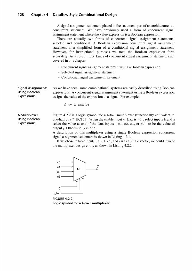
8/9/2019 VHDL for Engineers - Kenneth L. Short.pdf
http://slidepdf.com/reader/full/vhdl-for-engineers-kenneth-l-shortpdf 161/719
128 Chapter 4 Dataflow Style Combinational Design
A signal assignment statement placed in the statement part of an architecture is aconcurrent statement. We have previously used a form of concurrent signalassignment statement where the value expression is a Boolean expression.
There are actually two forms of concurrent signal assignment statements:selected and conditional. A Boolean expression concurrent signal assignmentstatement is a simplified form of a conditional signal assignment statement.However, for instructional purposes we treat the Boolean expression formseparately. As a result, three kinds of concurrent signal assignment statements arecovered in this chapter:
• Concurrent signal assignment statement using a Boolean expression
• Selected signal assignment statement
• Conditional signal assignment statement
Signal Assignments
Using BooleanExpressions
As we have seen, some combinational systems are easily described using Boolean
expressions. A concurrent signal assignment statement using a Boolean expressionassigns the value of the expression to a signal. For example:
f <= a and b;
A MultiplexerUsing BooleanExpressions
Figure 4.2.2 is a logic symbol for a 4-to-1 multiplexer (functionally equivalent toone-half of a 74HC153). When the enable input g_bar is '0', select inputs b and a
select the value at one of the data inputs—c3, c2, c1, or c0—to be the value of output y. Otherwise, y is '0'.A description of this multiplexer using a single Boolean expression concurrent
signal assignment statement is shown in Listing 4.2.1.If we chose to treat inputs c3, c2, c1, and c0 as a single vector, we could rewrite
the multiplexer design entity as shown in Listing 4.2.2.
FIGURE 4.2.2
Logic symbol for a 4-to-1 multiplexer.
Muxy
ab
g_bar
c0
c1
c2
c3

8/9/2019 VHDL for Engineers - Kenneth L. Short.pdf
http://slidepdf.com/reader/full/vhdl-for-engineers-kenneth-l-shortpdf 162/719
Section 4.2 Signal Assignments in Dataflow Style Architectures 129
LISTING 4.2.1A 4-to-1 multiplexer using a Boolean expression.
library ieee;use ieee.std_logic_1164.all;
entity mux4to1 is
port (c3, c2, c1, c0: in std_logic; g_bar, b, a: in std_logic; y: out std_logic);end mux4to1;
architecture dataflow of mux4to1 is
begin
y <= not g_bar and ( (not b and not a and c0) or (not b and a and c1) or (b and not a and c2) or (b and a and c3));
end dataflow;
LISTING 4.2.2A 4-to-1 multiplexer with data inputs treated as a vector.
library ieee;
use ieee.std_logic_1164.all;
entity mux4to1 is
port (c: in std_logic_vector(3 downto 0); g_bar, b, a: in std_logic; y: out std_logic);end mux4to1;
architecture dataflow2 of mux4to1 is
begin
y <= not g_bar and (
(not b and not a and c(0)) or (not b and a and c(1)) or (b and not a and c(2)) or (b and a and c(3)));
end dataflow2;

8/9/2019 VHDL for Engineers - Kenneth L. Short.pdf
http://slidepdf.com/reader/full/vhdl-for-engineers-kenneth-l-shortpdf 163/719
130 Chapter 4 Dataflow Style Combinational Design
Note the differences in notation used to represent inputs as elements of a vector inthe signal assignment statement in Listing 4.2.2 and as scalars in Listing 4.2.1.
4 .3 S ELE CT ED S IG NA L A SS IGN ME NT
A selected signal assignment statement, also called a with-select-when statement,allows one of several possible values to be assigned to a signal based on a select
expression. A simplified form of the selected signal assignment syntax is given inFigure 4.3.1.
Select Expression The select expression must be a discrete type or a one-dimensional character arraytype. Accordingly, there will be only a finite number of possible values for the select
expression.
Selected SignalAssignmentChoices
The choices specified must be locally static values of the select expression. Thismeans that their values must be determinable when the architecture containing theselected signal assignment statement is compiled.
One and only one of the choices in a selected signal assignment statement mustmatch the value of the select expression. Accordingly, the choices listed must bemutually exclusive.
Listing Choices A list of choices can be associated with a single value_expression by separating each
choice in the list using the vertical bar symbol ( | ).
DescribingCombinationalLogic Using aSelected SignalAssignment
To describe combinational logic, the choices listed in a selected signal assignment
must be all inclusive. That is, they must include every possible value of the select
expression. Exactly one choice must appear for each possible value of the selectexpression. This ensures that each time the assignment statement is executed, itstarget is assigned a value.
selected_signal_assignment ::=
with expression select target <= { value _expression when choices , }
value _expression when choices ;
FIGURE 4.3.1
Simplified syntax for selected signal assignment.
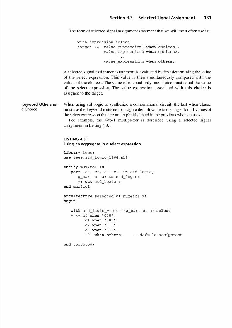
8/9/2019 VHDL for Engineers - Kenneth L. Short.pdf
http://slidepdf.com/reader/full/vhdl-for-engineers-kenneth-l-shortpdf 164/719
Section 4.3 Selected Signal Assignment 131
The form of selected signal assignment statement that we will most often use is:
with expression select
target <= value_expression1 when choices1, value_expression2 when choices2,
... value_expressionn when others;
A selected signal assignment statement is evaluated by first determining the valueof the select expression. This value is then simultaneously compared with thevalues of the choices. The value of one and only one choice must equal the valueof the select expression. The value expression associated with this choice isassigned to the target.
Keyword Others as
a Choice
When using std_logic to synthesize a combinational circuit, the last when clause
must use the keyword others to assign a default value to the target for all values of the select expression that are not explicitly listed in the previous when clauses.For example, the 4-to-1 multiplexer is described using a selected signal
assignment in Listing 4.3.1.
LISTING 4.3.1Using an aggregate in a select expression.
library ieee;use ieee.std_logic_1164.all;
entity mux4to1 is
port (c3, c2, c1, c0: in std_logic; g_bar, b, a: in std_logic; y: out std_logic);end mux4to1;
architecture selected of mux4to1 is
begin
with std_logic_vector'(g_bar, b, a) select
y <= c0 when "000",
c1 when "001", c2 when "010", c3 when "011", '0' when others; -- default assignment
end selected;

8/9/2019 VHDL for Engineers - Kenneth L. Short.pdf
http://slidepdf.com/reader/full/vhdl-for-engineers-kenneth-l-shortpdf 165/719
132 Chapter 4 Dataflow Style Combinational Design
Type Qualification In Listing 4.3.1, we want to use an aggregate formed from the enable and select inputsignals as the select expression:
(g_bar, b, a);
However, if we use this aggregate alone, the compiler cannot tell the aggregate’s typefrom the context. The compiler does not simply assume that an aggregate of std_logic elements is type std_logic_vector, since there are other array types, such asunsigned, that have std_logic elements.
We must explicitly specify the aggregate’s type. This is accomplished using atype qualification. A type qualification consists of writing the intended type namefollowed by a single quote character preceding an expression enclosed in paren-theses. The single quote ( ' ) is sometimes referred to as a tick . For example:
std_logic_vector'(g_bar, b, a)
specifies that the aggregate is type std_logic_vector.If the multiplexer is enabled (g_bar = '0'), and inputs b, a have the values '1'and '0', respectively, the select expression is the std_logic_vector "010", and thevalue of c2 is assigned to y.
Because every possible value of the select expression must be accounted for in thelisted choices, the last clause of the selected signal assignment statement uses thekeyword others to assign the value of '0' to y for the 725 values of the selectexpression not explicitly listed. While only 8 of the input combinations make senseto a synthesis tool, for the code to be strictly VHDL compliant it must account for allpossible values.
4 .4 TY PE B OO LE AN A ND T HE R EL AT IO NA L O P E R A T O R S
Conditional signal assignments, discussed in the next section, require evaluation of one or more conditions. A condition is an expression involving objects and relationaloperators. The result from evaluating a condition is type boolean.
Type boolean is an enumeration type predefined in package STANDARD as:
type boolean is (false, true);
Type boolean is an abstract type and is not used to directly represent signals insynthesizable descriptions. In VHDL, boolean and bit are different types, so booleanvalues true and false are not equivalent to bit values '1' and '0'.
The logical operators also apply to type boolean. Table 4.1.1 can be used to definethe logical operators for type boolean by replacing the 1s and 0s with true and false,respectively.

8/9/2019 VHDL for Engineers - Kenneth L. Short.pdf
http://slidepdf.com/reader/full/vhdl-for-engineers-kenneth-l-shortpdf 166/719
Section 4.4 Type Boolean and the Relational Operators 133
Relational
Operators
Package STANDARD also implicitly defines a set of relational operators, as shown
in Table 4.4.1.Relational operators are used to test the equality, inequality, or ordering of twoscalar types or composites of discrete types. Operand types must be the same. Theresult of a relational operation is always type boolean.
The equality and inequality operators are defined for all types except file. Incontrast, the other relational operators are only defined for scalars or composites of any discrete type. Since package STD_LOGIC_1164 does not overload any of therelational operators, the predefined interpretations of these operators apply to typestd_logic.
RelationalOperations onEnumerations
For scalars of enumeration types the interpretation of equality and inequality isstraightforward. For example, the equality operator returns true if the two operandsare the same and returns false otherwise.
Interpretations for the operators less than and greater than are based on theoperands’ position numbers in the enumeration type definition. The leftmost literalin an enumeration listing is in position 0. The position of each additional literal isone higher than the literal to its left. As a result, each enumeration type definitiondefines an ascending range of position numbers. When comparing two scalarenumeration literals, the one with a higher position number in the type definition isgreater than the other. Thus, in std_logic, 'Z' (with position number 4) is greaterthan '1' (with position number 3).
RelationalOperations onArrays
The interpretation of relational operators on arrays is a little more complex.However, we are interested only in the interpretation as it applies to one-dimensionalarrays of equal length. For equality, two arrays are equal if each pair of matchingelements in the two arrays is equal. If any pair of matching elements is not equal,then the two arrays are not equal.
Table 4.4.1VHDL relational operators.
Operator Operation Left Operand Right Operand Result
= equality any except file same as left boolean /= inequality
< less than scalar or same as left boolean
<= less than or equal composite
> greater than discrete type
>= greater than or equal

8/9/2019 VHDL for Engineers - Kenneth L. Short.pdf
http://slidepdf.com/reader/full/vhdl-for-engineers-kenneth-l-shortpdf 167/719
134 Chapter 4 Dataflow Style Combinational Design
Ordering ofOne-dimensionalArrays
Evaluation of the ordering operators applied to one-dimensional arrays of equallength is done starting with the leftmost elements of the arrays and preceding to theright until the determination can be made. For example, given two signal vectors:
signal a, b : std_logic_vectors (3 downto 0);
To determine if a < b, element a(3) is first compared to b(3). If a(3) is less thanb(3), then a < b.
However, if a(3) = b(3), then a(2) is compared with b(2). If a(2) < b(2),then a < b. This process is continued, comparing the next corresponding elements tothe right until the determination can be made.
Less Than or EqualOperator (<=)
The evaluation of a <= b is true if either a < b or a = b is true.Note that the interpretation of the operator <= as either the “less than or equal”
operator or as the “assignment” operator is based on the context in which it is used.
A description of a 4-bit magnitude comparator using relational operators actingon vectors (one-dimensional arrays) was given in Listing 3.7.1.
4 .5 C ON DI TI ON AL S IG NA L AS SI GN ME NT
A conditional signal assignment allows a signal to be assigned a value based on a setof conditions. The conditions are expressions involving relational operators. Condi-tional assignment is accomplished using a conditional signal assignment statement,
also called a when-else statement. A simplified form of the conditional signalassignment syntax is given in Figure 4.5.1.When there are zero occurrences of the “value_expression when condition else”
clause and no final “when condition” clause, this syntax reduces to:
target <= value_expression;
which is the syntax of the simple Boolean signal assignment statement.
conditional_signal_assignment ::=
target <= { value _expression when condition else }
value _expression [ when condition ];
FIGURE 4.5.1
Simplified syntax for conditional signal assignment.

8/9/2019 VHDL for Engineers - Kenneth L. Short.pdf
http://slidepdf.com/reader/full/vhdl-for-engineers-kenneth-l-shortpdf 168/719
Section 4.5 Conditional Signal Assignment 135
DescribingCombinationalLogic Usinga ConditionalSignal Assignment
To describe combinational logic using a conditional signal assignment statement,
the last value_expression must not have an associated when condition. Thisensures that every time the conditional signal assignment statement is executed itstarget is assigned a value.
The form of conditional signal assignment that we will most often use is:
target <= value_expression1 when condition1 else
value_expression2 when condition2 else
... value_expressionn-1 when conditionn-1 else value_expressionn;
A conditional signal assignment statement is evaluated by first evaluating its firstcondition. If this condition evaluates true, the associated value expression isassigned to the target and the execution is complete. If the first condition evaluatesfalse, the next condition is evaluated. This sequence of evaluations is continued
until a condition evaluates true, at which point its associated value expression isassigned to the target and execution is complete. If none of the conditions evaluatestrue, and the last value expression does not have a when condition clause, this valueis assigned to the target.
For example, Listing 4.5.1 illustrates the use of three separate conditional signalassignment statements, each containing one occurrence of the “value_expression when condition else” clause, to describe a 4-bit comparator that has three outputs.
LISTING 4.5.1A 4-bit comparator using multiple conditional signal assignment statements.
library ieee;use ieee.std_logic_1164.all;
entity mag_comp is
port ( p, q : in std_logic_vector (3 downto 0); p_gt_q_bar, p_eq_q_bar, p_lt_q_bar : out std_logic);end mag_comp;
architecture conditional of mag_comp is
begin
p_gt_q_bar <= '0' when p > q else '1'; p_eq_q_bar <= '0' when p = q else '1'; p_lt_q_bar <= '0' when p < q else '1';
end conditional;

8/9/2019 VHDL for Engineers - Kenneth L. Short.pdf
http://slidepdf.com/reader/full/vhdl-for-engineers-kenneth-l-shortpdf 169/719
136 Chapter 4 Dataflow Style Combinational Design
This comparator uses relational operators to compare the 4-bit std_logic_vectorsp and q. These std_logic_vectors are interpreted as representing unsigned binaryvalues. The comparator has three outputs, each asserted low. Output p_gt_q_bar isasserted if p is greater than q. Output p_lt_q_bar is asserted if p is less than q.Finally, output p_eq_q_bar is asserted if p is equal to q.
As another example, the 4-to-1 multiplexer is described using a single conditionalsignal assignment statement with multiple conditions in Listing 4.5.2.
A signal tmp is declared that is a three-element std_logic_vector. Port signalsg_bar, b, and c are aggregated and assigned to tmp.
The conditional signal assignment statement compares aggregate tmp to differentliteral vector values, as shown in Listing 4.5.2. For example, the third condition istrue if tmp = "010", which indicates that g_bar = '0', b = '1', and a = '0'.
In this example, using the signal tmp is more concise than repeatedly using theaggregate with a std_logic_vector type qualifier:
std_logic_vector'(g_bar, b, a)
Avoiding ImpliedLatches
Since our goal is to synthesize a combinational system, it is critical that the last valueexpression provides a default value for the situation where the input value does notcause any of the specified conditions to be true. This means that the lastvalue_expression must not have an associated when condition clause.
LISTING 4.5.2A 4-to-1 multiplexer using an aggregate for control and select inputs.
library ieee;
use ieee.std_logic_1164.all;
entity mux4to1 is
port (c0, c1, c2, c3: in std_logic; g_bar, b, a: in std_logic; y: out std_logic);end mux4to1;
architecture conditional of mux4to1 is
signal tmp : std_logic_vector(2 downto 0); begin
tmp <= (g_bar, b, a); y <= c0 when tmp = "000" else
c1 when tmp = "001" else
c2 when tmp = "010" else
c3 when tmp = "011" else
'0'; -- default assignment
end conditional;

8/9/2019 VHDL for Engineers - Kenneth L. Short.pdf
http://slidepdf.com/reader/full/vhdl-for-engineers-kenneth-l-shortpdf 170/719
Section 4.5 Conditional Signal Assignment 137
For example, if the conditional signal assignment is written as:
y <= c0 when tmp = "000" else
c1 when tmp = "001" else
c2 when tmp = "010" else
c3 when tmp = "011";
The VHDL interpretation of this construct is that, for the four specified values of tmp, a new value should be assigned to y. However, for all other values of tmp thereshould be no new value assigned to y. This implies that the y should retain itsprevious value. Thus, a synthesizer’s interpretation is that the circuit needs toremember the previous value of y. As a result, the synthesizer generates a latch at theoutput of the combinational logic to store the value of y.
Figure 4.5.2 shows the logic synthesized for a modified version of Listing 4.5.2that uses the previous conditional signal assignment, where the last value expression
has a when clause.
FIGURE 4.5.2
Synthesized multiplexer logic with undesired implied latch.
g_bar
c0
c2c1c3
e
d
ed lat
y
y_1
un1_un1_a
un1_a_1
un1_b_2
un1_b_1
QD
Ce
d
e
d
a
b
y

8/9/2019 VHDL for Engineers - Kenneth L. Short.pdf
http://slidepdf.com/reader/full/vhdl-for-engineers-kenneth-l-shortpdf 171/719
138 Chapter 4 Dataflow Style Combinational Design
LISTING 4.5.3Two-input AND using conditional signal assignment without a defaultcondition.
library ieee;
use ieee.std_logic_1164.all;
entity and_2_bad is
port ( a: in std_logic; b: in std_logic; c: out std_logic);end and_2_bad;
architecture and_2_bad of and_2_bad is
signal tmp : std_logic_vector(1 downto 0);
begin
tmp <= (a, b); c <= '0' when tmp = "00" else
'0' when tmp = "01" else
'0' when tmp = "10" else
'1' when tmp = "11";end and_2_bad;
The form of multiplexer symbol used in Figure 4.5.2 has each data input (d)paired with an enable input (e). Only one enable input is asserted at any time. Thedata at the data input whose associated enable is asserted appears at the multiplexer’s
output.The memory element synthesized when a default assignment is omitted is a latch.
The synthesized circuit still works properly when g_bar is asserted (because thenthe latch is transparent). However, instead of producing y = '0' when g_bar isunasserted, the circuit holds y at the value it had at the time g_bar was unasserted.Of course, the unwanted latch also makes the circuit slower.
The All PossibleInput CombinationsTrap
Consider the description in Listing 4.5.3 for a two-input AND gate. This descriptionuses a conditional signal assignment statement that has a final when condition clause(Figure 4.5.1). There is a subtle trap here for the unwary.
At first glance, it may appear that all the possible input value combinations for atwo-input gate have been specified as conditions in the conditional signal assignmentstatement. However, this design may also cause memory to be synthesized.
The catch is that all input combinations have been specified only if the gate’s inputsare of a type (such as bit) that has only the values '0' and '1'. However, this gate’sinputs are type std_logic. Each std_logic input has nine possible values. So, for a two-input gate there are 92 = 81 different input combinations. Only four have been listed.Some synthesizers may add a latch to remember the previous value of y for those cases

8/9/2019 VHDL for Engineers - Kenneth L. Short.pdf
http://slidepdf.com/reader/full/vhdl-for-engineers-kenneth-l-shortpdf 172/719
Section 4.6 Priority Encoders 139
where the input is one of the 77 other possible values. Other synthesizers may correctlyinterpret the intent of what was written and synthesize only an AND gate.
4 . 6 P R I O R IT Y E N C OD E RS
Three forms of concurrent signal assignment statements have been introduced. For acombinational design, any of these constructs might be used. However, for somefunctions, one may be more concise or intuitive than the others. For a particularfunction, the circuits synthesized from all of these constructs are functionally equivalent.
Inherent Priority ofConditional SignalAssignment
Because a conditional signal assignment statement assigns the value associated withits first condition that is true, it inherently establishes a priority. This makes a condi-tional signal assignment statement ideal for describing priority circuits.
Consider a 4-to-2 priority encoder that has four inputs i3, i2, i1, and i0 andoutputs a1, a0. The outputs are the complement of the binary encoding of the suffixof the highest priority input asserted. Inputs are asserted low. Functionally, thisencoder is a smaller and more limited version of the 74HC148 eight-line to three-line priority encoder.
Input i3 has the highest priority and input i0 has the lowest. For example, if inputs i3 and i2 are simultaneously asserted, the output is "00". This is so because"00" is the complement of "11", which is the binary encoding of the numeric suffix3 of i3. The VHDL code for this circuit is given in Listing 4.6.1.
LISTING 4.6.1A 4-to-2 priority encoder using a conditional signal assignment.
library ieee;use ieee.std_logic_1164.all;
entity encoder is
port ( i3, i2, i1, i0 : in std_logic; a : out std_logic_vector(1 downto 0));end;
architecture csa_cond of encoder is
--signal outputs: std_logic_vector(1 downto 0); begin
a <= "00" when i3 = '0' else
"01" when i2 = '0' else
"10" when i1 = '0' else
"11";end csa_cond;

8/9/2019 VHDL for Engineers - Kenneth L. Short.pdf
http://slidepdf.com/reader/full/vhdl-for-engineers-kenneth-l-shortpdf 173/719
140 Chapter 4 Dataflow Style Combinational Design
The conditional signal assignment statement first tests whether i3 = '0'. If thisis true, the output is assigned the value "00". Only if i3 does not equal '0' is thesecond condition tested. The second condition tests whether i2 = '0'. If i2 = '0',then the output is assigned the value "01". However, since the second condition isonly tested after the first condition fails, the output is only assigned the value "01"
when i3 = '1' and i2 = '0'. This property of the conditional signal assignmentstatement provides inherent priority.
4 .7 D ON ’T CA RE I NP UT S A ND OU TP UT S
As previously discussed, std_logic values '1', 'H', '0', and 'L' are interpreted asrepresenting one of two logic levels. In contrast, std_logic metalogic values 'U','X', 'W', and '-' are interpreted as defining the behavior of a model itself, ratherthan the behavior of the hardware being synthesized.
Don’t Care Value In traditional logic design, a “don’t care” is used to specify a value in a situationwhere we don’t care whether the value is a '0' or a '1'. In VHDL, '-' representsthe “don’t care” value. There are some important differences in interpretation of a“don’t care” in VHDL compared to traditional logic design. Importantly, the “don’tcare” value is treated differently by a simulator than by a synthesizer.
SimulatorInterpretation of a
'-'
Simulators treat a '-' input or output as a literal value. So, to a simulator, '-'literally means the character '-', rather than meaning that the character '-' can be
replaced by either a '0' or '1'. When '-' appears as an output in a description, asimulator’s interpretation is that this symbol is being used to indicate that a choicefor that output’s state has not been made.
SynthesizerInterpretation of a'-'
Normally, a synthesizer is supposed to synthesize logic that behaves the same way asdoes the design description’s simulation. A synthesizer also treats a '-' input as aliteral value.
In contrast, a synthesizer treats a '-' output as a true “don’t care” condition forlogic minimization purposes. This allows the synthesizer to take advantage of anydon’t care output assignments to minimize the logic it synthesizes.
IEEE Std 1076.3Interpretationof MetalogicalValues
The IEEE Standard Synthesis Package (IEEE Std 1076.3) requires that, if ametalogical value occurs as a choice in a statement interpreted by a synthesizer, thesynthesizer shall interpret the choice as one that will never occur. For a metalogicalvalue in an assignment statement, the synthesizer shall accept the value, but is notrequired to provide any particular interpretation.

8/9/2019 VHDL for Engineers - Kenneth L. Short.pdf
http://slidepdf.com/reader/full/vhdl-for-engineers-kenneth-l-shortpdf 174/719
Section 4.7 Don’t Care Inputs and Outputs 141
Don’t Care Inputs Listing 4.7.1 shows an attempt to use “don’t cares” to describe a 4-to-2 priorityencoder.
A simulator compiles this design without any syntax errors. However, when wesimulate this description by applying all input combinations where each input iseither a '0' or a '1', the output is always "11". This result occurs because theliteral input values ("0---" or "10--" or "110-") that can cause an output otherthan "11" are never applied as inputs during the simulation.
When this design is synthesized, the synthesizer’s compiler also generates nosyntax errors. However, because the synthesizer interprets conditions involving a'-' input value (such as "0---") as conditions that can never occur in a physicalcircuit, it generates warnings that the inputs are unused and synthesizes a circuit withits outputs hardwired to "11".
Std_matchFunction
But what if, for the purpose of making comparisons of std_logic_vectors, we want'-' inputs to be treated by both the simulator and synthesizer as “don’t cares” in the
traditional sense? A function is available in package NUMERIC_STD that can beused to accomplish this. The function is named std_match. To use this function, ause clause specifying package NUMERIC_STD must be included in the description.Package NUMERIC_STD is discussed further in Chapter 13.
LISTING 4.7.1A 4-to-2 priority encoder—an incorrect approach using “don’t care” inputs.
library ieee;use ieee.std_logic_1164.all;
entity encoder is
port ( i3, i2, i1, i0 : in std_logic; a : out std_logic_vector(1 downto 0));end;
architecture csa_cond of encoder is
signal tempi: std_logic_vector(3 downto 0);begin
tempi <= (i3, i2, i1, i0);
a <= "00" when tempi = "0---" else
"01" when tempi = "10--" else
"10" when tempi = "110-" else
"11";
end csa_cond;

8/9/2019 VHDL for Engineers - Kenneth L. Short.pdf
http://slidepdf.com/reader/full/vhdl-for-engineers-kenneth-l-shortpdf 175/719
142 Chapter 4 Dataflow Style Combinational Design
The std_match function can be used to compare two scalars, which are typestd_ulogic, or two vectors whose elements are type std_ulogic. Thus, since std_logicis a subtype of std_ulogic, this function can be used to compare std_logic vectors.
If the vectors match, a boolean true is returned. Element values in correspondingpositions in a vector are considered a match if they are not metalogical and are equal,or if one is not metalogical and the other is '-', or if both element values are '-'s.In effect, '-' acts as a “wild card” for the comparison.
Vectors match if their element values in all corresponding positions match. Forexample, the value "10--" is considered by the std_match function to match allthe following values: "101-", "1010", and "1001".
We can’t use the std_match function to represent choices in a selected signalassignment, because these choices must be statically deterministic. A description of a 4-to-2 priority encoder using the std_match functions in a conditional signalassignment is given in Listing 4.7.2.
While the code in Listing 4.7.2 is valid, it is not an improvement in terms of
conciseness over that in Listing 4.6.1.
LISTING 4.7.2A 4-to-2 priority encoder using the std_match function to interpret “don’t care”inputs, '-'.
library ieee;use ieee.std_logic_1164.all;use ieee.numeric_std.all;
entity encoder is
port ( i3, i2, i1, i0 : in std_logic; a : out std_logic_vector(1 downto 0));end entity;
architecture cond_match of encoder is
signal tempi: std_logic_vector(3 downto 0); begin
tempi <= (i3, i2, i1, i0);
a <= "00" when std_match (tempi, "0---") else
"01" when std_match (tempi, "10--") else
"10" when std_match (tempi, "110-") else
"11";
end cond_match;
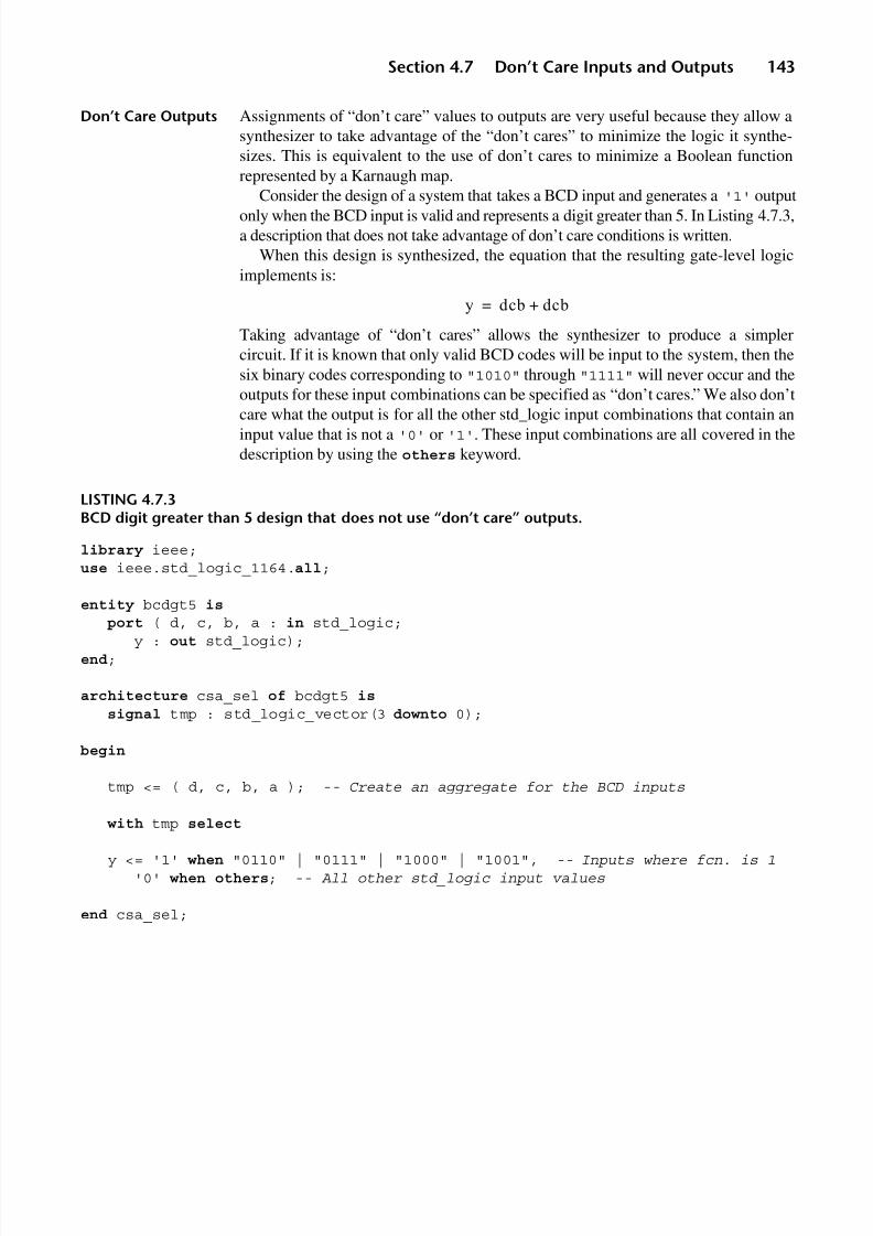
8/9/2019 VHDL for Engineers - Kenneth L. Short.pdf
http://slidepdf.com/reader/full/vhdl-for-engineers-kenneth-l-shortpdf 176/719
Section 4.7 Don’t Care Inputs and Outputs 143
Don’t Care Outputs Assignments of “don’t care” values to outputs are very useful because they allow asynthesizer to take advantage of the “don’t cares” to minimize the logic it synthe-sizes. This is equivalent to the use of don’t cares to minimize a Boolean functionrepresented by a Karnaugh map.
Consider the design of a system that takes a BCD input and generates a '1' outputonly when the BCD input is valid and represents a digit greater than 5. In Listing 4.7.3,a description that does not take advantage of don’t care conditions is written.
When this design is synthesized, the equation that the resulting gate-level logicimplements is:
Taking advantage of “don’t cares” allows the synthesizer to produce a simplercircuit. If it is known that only valid BCD codes will be input to the system, then thesix binary codes corresponding to "1010" through "1111" will never occur and theoutputs for these input combinations can be specified as “don’t cares.” We also don’t
care what the output is for all the other std_logic input combinations that contain aninput value that is not a '0' or '1'. These input combinations are all covered in thedescription by using the others keyword.
LISTING 4.7.3BCD digit greater than 5 design that does not use “don’t care” outputs.
library ieee;use ieee.std_logic_1164.all;
entity bcdgt5 is
port ( d, c, b, a : in std_logic; y : out std_logic);end;
architecture csa_sel of bcdgt5 is
signal tmp : std_logic_vector(3 downto 0);
begin
tmp <= ( d, c, b, a ); -- Create an aggregate for the BCD inputs
with tmp select
y <= '1' when "0110" | "0111" | "1000" | "1001", -- Inputs where fcn. is 1 '0' when others; -- All other std_logic input values
end csa_sel;
y dcb dcb+=

8/9/2019 VHDL for Engineers - Kenneth L. Short.pdf
http://slidepdf.com/reader/full/vhdl-for-engineers-kenneth-l-shortpdf 177/719
144 Chapter 4 Dataflow Style Combinational Design
LISTING 4.7.4BCD digit greater than 5 design that uses “don’t care” outputs.
library ieee;use ieee.std_logic_1164.all;
entity bcdgt5 is
port ( d, c, b, a : in std_logic; y : out std_logic);end;
architecture csa_sel of bcdgt5 is
signal tmp : std_logic_vector(3 downto 0);begin
tmp <= ( d, c, b, a );-- Outputs for the ten inputs that can actually -- occur in the circuit are specified
with tmp select
y <= '0' when "0000" | "0001" | "0010" | "0011" | "0100" | "0101", '1' when "0110" | "0111" | "1000" | "1001", '-' when others; -- Don't care for input conditons that -- cannot occur end csa_sel;
The description in Listing 4.7.4 specifies a don’t care output value '-' for theothers choice.
Listing 4.7.4 is longer than Listing 4.7.3, because the cases where the output must
be '0' must be distinguished from the “don’t care” cases. However, the gate-levellogic synthesized from Listing 4.7.4 realizes the simpler equation:
As this equation indicates, the output from the synthesized hardware never actuallyhas the value '-'. For each input condition where the output is specified as don’tcare, the minimization algorithm has chosen a value of either '0' or '1' for theoutput, whichever results in the simplest function.
'X' as a “Don’tCare” for Outputs
Some synthesizers also accept use of the std_logic value 'X' to specify a “don’tcare” output. X is also traditionally used on IC data sheets to indicate a “don’t care”value, as opposed to its primary use in VHDL to represent a forcing unknown.
4 . 8 D E C OD E R S
Like encoders, decoders are readily described using dataflow style architectures.Two example decoder designs are given in this section.
y d cb+=

8/9/2019 VHDL for Engineers - Kenneth L. Short.pdf
http://slidepdf.com/reader/full/vhdl-for-engineers-kenneth-l-shortpdf 178/719
Section 4.8 Decoders 145
74HC138 DecoderEquivalent
Consider a decoder function like that of the 74HC138 three-line to eight-linedecoder. It has three enable inputs: g1, g2a_bar, g2b_bar. When g1, g2a_bar,g2b_bar equal "100", the decoder is enabled. For any other combination of theenable inputs, the decoder is disabled.
When disabled, the decoder’s eight outputs (y7 down to y0) are all '1's. Whenenabled, one of its outputs is '0' and all the others are '1's. The output that is '0'is determined by the binary value of the three select inputs: c, b, and a. For example,if the decoder is enabled and c, b, a equals "110", then output y6 is a logic '0'. Adescription of this decoder is given in Listing 4.8.1.
The select and the enable inputs are declared as scalars in the entity declaration. Inthe architecture declarative part, two signals, enables and cba, are each declared asthree-element std_logic_vectors. In the architecture statement part, two aggregates
LISTING 4.8.1
A 3-to-8 decoder description.
library ieee;use ieee.std_logic_1164.all;
entity decoder_3to8 is
port ( c, b, a: in std_logic; g1, g2a_bar, g2b_bar: in std_logic; y: out std_logic_vector (7 downto 0));end decoder_3to8;
architecture csa_cond of decoder_3to8 is
signal enables, cba : std_logic_vector(2 downto 0);
begin
enables <= (g1, g2a_bar, g2b_bar); cba <= (c, b, a);
y <= "11111110" when enables = "100" and cba = "000" else
"11111101" when enables = "100" and cba = "001" else
"11111011" when enables = "100" and cba = "010" else "11110111" when enables = "100" and cba = "011" else
"11101111" when enables = "100" and cba = "100" else
"11011111" when enables = "100" and cba = "101" else
"10111111" when enables = "100" and cba = "110" else
"01111111" when enables = "100" and cba = "111" else
"11111111";
end csa_cond;

8/9/2019 VHDL for Engineers - Kenneth L. Short.pdf
http://slidepdf.com/reader/full/vhdl-for-engineers-kenneth-l-shortpdf 179/719
146 Chapter 4 Dataflow Style Combinational Design
are used. One aggregates the enable inputs into the std_logic_vector enables. Theother aggregates the select inputs into the std_logic_vector cba.
A single conditional signal assignment statement is then used to describe thedecoder function. Each of the eight conditions, corresponding to the assertion of oneof the decoder’s outputs, is the logical AND of a condition for the enable inputs anda condition for the select inputs. The default assignment handles the case when the
decoder is not enabled.A single aggregate could be used to aggregate all six inputs, but the functionality
of the design would probably be less clear when reading the code.
BCD toSeven-SegmentDecoder
An often used decoder function is a BCD to seven-segment decoder. This decodertakes as its inputs four bits that represent a binary coded decimal (BCD) value andgenerates a 7-bit output to drive a seven-segment LED. The segments of a seven-segment LED are shown in Figure 4.8.1.
A description of a BCD to seven-segment decoder is given in Listing 4.8.2.The decoder’s BCD input is the std_logic_vector dcba. There are two other
inputs to the decoder. When asserted, blanking input bi_bar forces all the decoder’soutputs to '1's. A '1' output turns OFF its associated LED segment; a '0' output
LISTING 4.8.2Description of a BCD to seven-segment decoder.
library ieee;use ieee.std_logic_1164.all;
entity bcd_7seg is
port ( bi_bar : in std_logic; -- blanking input
lt_bar : in std_logic; -- lamp test input dcba : in std_logic_vector (3 downto 0); --BCD input seg: out std_logic_vector(6 downto 0) -- segments in order from a to g );end bcd_7seg;
architecture conditional of bcd_7seg is
FIGURE 4.8.1
Segment pattern for a seven-segment display.
b
a
g
d
c
f
e

8/9/2019 VHDL for Engineers - Kenneth L. Short.pdf
http://slidepdf.com/reader/full/vhdl-for-engineers-kenneth-l-shortpdf 180/719
Section 4.9 Table Lookup 147
begin
seg <= "1111111" when bi_bar = '0' else
"0000000" when lt_bar = '0' else
"0000001" when (dcba = "0000") else
"1001111" when (dcba = "0001") else
"0010010" when (dcba = "0010") else "0000110" when (dcba = "0011") else
"1001100" when (dcba = "0100") else
"0100100" when (dcba = "0101") else
"1100000" when (dcba = "0110") else
"0001111" when (dcba = "0111") else
"0000000" when (dcba = "1000") else
"0001100" when (dcba = "1001") else
"-------";
end conditional;
turns ON its associated LED segment. If the blanking input is not asserted and lamptest input lt_bar is asserted, all the outputs are '0's, forcing all the LED segmentsto be ON. If neither the blanking input nor the lamp test input is asserted, the outputis determined by the value of the BCD input. If the BCD input has a value from 0 to9 ("0000" to "1001"), the output consists of the values needed to display the corre-sponding decimal digit. If the BCD input is greater than 9, all the outputs are don’tcares, since these input values should not occur.
The priority characteristic of a conditional signal assignment is particularlyhelpful for this design since the bi_bar input has priority over the lt_bar input,
which has priority over the dcba input.
4 . 9 TA BL E L OO K UP
A simple way to describe a combinational system is to use a table lookup. For asystem with a single output the table is represented as a constant vector. For a systemwith multiple outputs an array of constant vectors is used. For any input combinationwe can then determine the output by simply looking it up in the table.
Consider the combinational system represented by the truth table in Table 4.9.1.This system has a single output that is specified to be a don’t care value for two of
its input combinations. A description of this system is given in Listing 4.9.1.A constant vector named output with a range from 0 to 7 is declared. The value
of this vector, "01-01-10", corresponds to the values of output y for each possiblecombination of the inputs. These values are simply the values of the column labeledy taken from top to bottom. That is, from row 0 to row 7.

8/9/2019 VHDL for Engineers - Kenneth L. Short.pdf
http://slidepdf.com/reader/full/vhdl-for-engineers-kenneth-l-shortpdf 181/719
148 Chapter 4 Dataflow Style Combinational Design
If the binary input value is converted to an integer, this integer can be used as anindex into the table to select the table entry that is the desired output. The archi-tecture body consists of a single statement:
y <= output(to_integer(unsigned'(a, b, c)));
This statement first aggregates the inputs a, b, c and type qualifies them as anunsigned vector, so that the to_integer function can be used to convert the inputvalues to an integer. This integer is then used as the index into the constant vector tolook up the appropriate value for the output.
LISTING 4.9.1Table lookup for a system with a single output.
library ieee;use ieee.std_logic_1164.all;use ieee.numeric_std.all;
entity table_lookup_vector is
port( a, b, c : in std_logic;y : out std_logic );
end table_lookup_vector;
architecture lookup of table_lookup_vector is
constant output : std_logic_vector(0 to 7) := "01-01-10";begin
y <= output(to_integer(unsigned'(a, b, c)));
end lookup;
Table 4.9.1Truth table for a systemwith a single output.
a b c y
0 0 0 0
0 0 1 1
0 1 0 -
0 1 1 0
1 0 0 1
1 0 1 -
1 1 0 1
1 1 1 0

8/9/2019 VHDL for Engineers - Kenneth L. Short.pdf
http://slidepdf.com/reader/full/vhdl-for-engineers-kenneth-l-shortpdf 182/719
Section 4.9 Table Lookup 149
For a system with multiple outputs, an array of constant vectors can be used todefine the table that describes the system. Consider the truth table representation of the combinational function that converts a 2-bit binary value to a 2-bit reflected
code, Table 4.9.2.A description of this table lookup is given in Listing 4.9.2.
LISTING 4.9.2A 2-bit binary to reflected code conversion described as a table lookup.
library ieee;use ieee.std_logic_1164.all;use ieee.numeric_std.all;
entity bin2reflected is
port (input: in std_logic_vector (1 downto 0); output: out std_logic_vector (1 downto 0));end bin2reflected;
architecture look_up of bin2reflected is
type bin2refl is array (0 to 3) of std_logic_vector(1 downto 0);
-- table of valuesconstant reflected_tt : bin2refl := ("00","01","11","10");
begin
output <= reflected_tt(to_integer(unsigned(input)));
end look_up;
Table 4.9.2Truth table for a 2-bit binaryto reflected code conversion.
input output
00 00
01 01
10 11
11 10

8/9/2019 VHDL for Engineers - Kenneth L. Short.pdf
http://slidepdf.com/reader/full/vhdl-for-engineers-kenneth-l-shortpdf 183/719
150 Chapter 4 Dataflow Style Combinational Design
In the architecture’s declarative part an array type named bin2refl is declared.
type bin2refl is array (0 to 3) of std_logic_vector(1 downto 0);
Type bin2refl is an array of vectors. This array type consists of four elements
representing rows (0 to 3) of a truth table. Each element (row) in this array is a two-element std_logic_vector, representing the outputs for that row of the truth table.
A constant named reflected_tt is then declared.
constant reflected_tt : bin2refl := ("00","01","11","10");
This constant is of the previously declared type bin2refl and its value is specified
by four 2-character strings.The architecture’s statement part consists of a single signal assignment statement:
output <= reflected_tt(to_integer(unsigned(input)));
To_integerFunction
In this assignment statement, the binary input vector input is first converted fromtype std_logic to type unsigned by a type conversion. Because these two types areclosely related, this type conversion can be accomplished by simply using the nameof the target type as if it were a function.
unsigned(input)
The unsigned result of this operation is then converted to an integer using thefunction to_integer. Function to_integer is defined in packageNUMERIC_STD. The integer result returned by the function is used as the index toselect the element (row vector) of constant array reflected_tt. This row vector isassigned to output. For example, if input equals "10" then the function
FIGURE 4.9.1
RTL hierarchical view of table lookup description of binary to reflected codedescription.
input[1:0] output[1:0]
rom
output_1[0]
A[1:0]
[1:0]
[1:0]
[1]
DOUT

8/9/2019 VHDL for Engineers - Kenneth L. Short.pdf
http://slidepdf.com/reader/full/vhdl-for-engineers-kenneth-l-shortpdf 184/719
Section 4.10 Three-State Buffers 151
to_integer returns the integer 2. For this input value, the assignment statement is
equivalent to:
output <= reflected_tt(2);
or
output <= "11";
One way to view the hardware implementation of the table lookup process is as read-only memory (ROM). The system’s inputs are the ROM’s address inputs and theROM’s contents are the table’s output values. For a particular input value (address)
the ROM outputs the data stored at that address.A synthesis tool may also view a table lookup in terms of ROM. A hierarchical
view of the description in Listing 4.9.2 is given in Figure 4.9.1. However, whentarget of the synthesis is a PLD, the synthesizer does not synthesize the circuit asROM. Instead, it implements the inferred logic in its reduced logic form.
The reduced logic created by the synthesizer is given in Figure 4.9.2.The reduced synthesized logic is:
4 . 10 T H RE E -S T AT E B U F FE R S
A three-state buffer (tristate buffer ) has a data input and an enable input. Its enableinput controls whether the three-state buffer is OFF and its output is high impedance('Z'), or whether it is ON and its output is driven by its data input. Thus, the outputof a three-state buffer can be either '0', '1', or 'Z'.
FIGURE 4.9.2
Technology dependent flattened-to-gates view of table lookup description ofbinary to reflected code description.
input[1:0]output[1:0]
output\[1\].O
output\[0\].Ooutput_1_0.G_9.Oinput\[0\].O
input\[1\].O
[1:0][1:0]
[1]
[1]
[0][0]
output(1) input(1)=
output(0) input(1) input(0)⋅ input(1) input(0)⋅+=
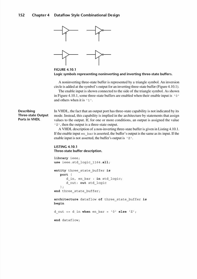
8/9/2019 VHDL for Engineers - Kenneth L. Short.pdf
http://slidepdf.com/reader/full/vhdl-for-engineers-kenneth-l-shortpdf 185/719
152 Chapter 4 Dataflow Style Combinational Design
A noninverting three-state buffer is represented by a triangle symbol. An inversioncircle is added at the symbol’s output for an inverting three-state buffer (Figure 4.10.1).
The enable input is shown connected to the side of the triangle symbol. As shown
in Figure 4.10.1, some three-state buffers are enabled when their enable input is '0'and others when it is '1'.
DescribingThree-state OutputPorts in VHDL
In VHDL, the fact that an output port has three-state capability is not indicated by itsmode. Instead, this capability is implied in the architecture by statements that assignvalues to the output. If, for one or more conditions, an output is assigned the value'Z', then the output is a three-state output.
A VHDL description of a non-inverting three-state buffer is given in Listing 4.10.1.If the enable input en_bar is asserted, the buffer’s output is the same as its input. If theenable input is not asserted, the buffer’s output is 'Z'.
LISTING 4.10.1Three-state buffer description.
library ieee;use ieee.std_logic_1164.all;
entity three_state_buffer is
port ( d_in, en_bar : in std_logic; d_out: out std_logic
);end three_state_buffer;
architecture dataflow of three_state_buffer is
begin
d_out <= d_in when en_bar = '0' else 'Z';
end dataflow;
FIGURE 4.10.1
Logic symbols representing noninverting and inverting three-state buffers.

8/9/2019 VHDL for Engineers - Kenneth L. Short.pdf
http://slidepdf.com/reader/full/vhdl-for-engineers-kenneth-l-shortpdf 186/719
Section 4.10 Three-State Buffers 153
Multiplexing Two
Data Sources
Multiplexing signals from two data sources using three-state buffers is achieved by
connecting the two three-state buffers’ outputs together to drive the shared signal,Figure 4.10.2. While this figure represents the three-state buffers as separate logicelements, they could be integrated into the outputs of two more functionally complexsystems.
When the type of connection in Figure 4.10.2 is made, the designer must addlogic that controls the three-state buffers’ enable inputs so that only one or none of the buffers is enabled at a time. If only one buffer is enabled, that output determinesthe logic level for the shared signal. If none of the buffers is enabled, both outputs arein their high impedance states and the shared signal they drive has the highimpedance value.
Bus Contention The prohibited situation, where two or more three-state outputs connected to ashared signal are simultaneously enabled, creates a serious problem if one of theenabled outputs is trying to drive the shared signal to '1' and another is trying todrive it to '0'. The resulting voltage level is in the forbidden region. This situationis referred to as bus contention. In std_logic terms, the shared signal’s value is 'X'(forcing unknown). In a hardware implementation, excessive current may flowbetween the two enabled three-state outputs under this condition.
The resolution function for std_logic properly models three-state outputs drivinga shared signal. In Table 3.4.2, if both outputs (drivers) are 'Z', the shared output is'Z'. If one output is 'Z' and the other is '1', the result is '1'. If one output is 'Z'
and the other is '0', the result is '0'. If both outputs are enabled and drive differentvalues, '0' and '1' or '1' and '0', the output is 'X'.
A structural description of the circuit in Figure 4.10.2 is given in Listing 4.10.2.The description assumes that the three-state buffer entity from Listing 4.10.1 hasbeen compiled to the library three_state_buffer.
Waveforms from the simulation of this description are presented in Figure 4.10.3.The input stimulus just counts through all possible binary input combinations.The first input combination has the data input to each buffer equal to '0' and both
FIGURE 4.10.2
Connecting the outputs of two three-state buffers to accomplish multiplexing.
d_a
d_bus
u1
u2d_b
en_a
en_b

8/9/2019 VHDL for Engineers - Kenneth L. Short.pdf
http://slidepdf.com/reader/full/vhdl-for-engineers-kenneth-l-shortpdf 187/719
154 Chapter 4 Dataflow Style Combinational Design
LISTING 4.10.2Two three-state buffers with their outputs connected.
library ieee;use ieee.std_logic_1164.all;
library three_state_buffer; -- library containing three-state buffer use three_state_buffer.all;
entity three_state_bus is
port ( d_a: in std_logic; -- data input buffer a en_a_bar: in std_logic; -- enable input buffer a d_b: in std_logic; -- data input buffer b en_b_bar: in std_logic; -- enable input buffer b d_bus: out std_logic -- bused data output );end three_state_bus;
architecture three_state_bus of three_state_bus is
begin
u1: entity three_state_buffer port map (d_a, en_a_bar, d_bus); u2: entity three_state_buffer port map (d_b, en_b_bar, d_bus);end three_state_bus;
enables are asserted. This corresponds to an invalid situation because the two buffersshould not be enabled simultaneously. However, the output is a valid '0' becauseboth buffers’ data inputs are '0'.
For the second input combination, indicated by the cursor, the input data at bufferu1 is a '1' and at buffer u2 is '0', and both buffers are enabled. The output for thiscase is 'X', because one buffer is trying to drive the output to a '1' and the other istrying to drive it to a '0'. On the output waveform, the times during which the outputis forcing an unknown value ('X') are represented by two lines, one at the '1' logiclevel and the other at the '0' logic level.
FIGURE 4.10.3
Timing waveform for two three-state buffers with their outputs connected.

8/9/2019 VHDL for Engineers - Kenneth L. Short.pdf
http://slidepdf.com/reader/full/vhdl-for-engineers-kenneth-l-shortpdf 188/719
Section 4.11 Avoiding Combinational Loops 155
For input conditions corresponding to one buffer enabled and the other notenabled, the output is the same as the enabled buffer’s input value. When bothbuffers are not enabled, the output is 'Z'. This value is represented on the waveformby a line halfway between the '0' and '1' logic levels.
Three-state OutputCapability of a PLD
If some of the outputs of a PLD need to be multiplexed with outputs from other ICs,these outputs can be described in VHDL as three-state outputs. Since almost allPLDs have output pins with three-state capability, the described functionality iseasily synthesized. One of the inputs to the PLD must be an enable signal to controlthe three-state outputs. Note that ports of a PLD described as mode out or inout(bidirectional) can be described as three-state outputs.
We will see a number of examples later in this book where the system beingdescribed in VHDL and implemented using a PLD connects to the system bus of amicroprocessor. Those signals that connect to the data bus portion of the system busmust be three-state.
Internal Three-stateBuffers in a PLD
If we need to implement a multiplexing operation within a design description, wemight choose to describe this operation using three-state buffers. However, whilePLDs have three-state buffers at their output pins, many PLDs do not have internalthree-state buffers. When such a description is synthesized, the synthesizer attemptsto replace the functionality implemented by the three-state buffers with a multiplexeror equivalent gate logic. Even so, some PLD manufacturers recommend that internalthree-state buffers not be used in a description.
Furthermore, if we are writing descriptions of entities to be used as componentsin a hierarchical system, we should refrain from using three-state buffers on their
outputs, unless the three-state outputs of the component entity will connect directlyto outputs of the top-level entity. This is because three-state outputs from compo-nents that do not connect directly to outputs of the top-level entry become internalthree-state buffers at the top level. In conclusion, it is best to use three-state buffersonly when they are driving top-level bidirectional or output pins.
4 . 1 1 A VO I D I NG C O MB I N AT I O N AL L O O P S
When synthesizing a description of a combinational system, the synthesizer may
issue a warning that the description contains a combinational loop. A combina-tional loop (Figure 4.11.1) is an output looped back (fed back) to one of theinputs. If we are attempting to describe a combinational system, our descriptionmust not contain any combinational loops. The existence of such a loop can leadto circuit instability.
Figure 4.11.1(a) shows the general case of a combinational loop. In thedescription of a complex system, it may not be obvious that such a loop exists. Fortu-nately, the synthesizer will detect the loop’s existence and issue a warning message.

8/9/2019 VHDL for Engineers - Kenneth L. Short.pdf
http://slidepdf.com/reader/full/vhdl-for-engineers-kenneth-l-shortpdf 189/719
156 Chapter 4 Dataflow Style Combinational Design
In Listing 4.11.1 of the circuit in Figure 4.11.1(b), existence of a combinationalloop is readily apparent.
Since port sigout is declared as mode out, it cannot be read in the architecture.Instead, signal s1 is declared and used to feed the NAND gate’s output back to oneof its inputs. Signal s1 can then be assigned to sigout.
LISTING 4.11.1Dataflow description of a NAND gate circuit containing a combinational loop.
library ieee;use ieee.std_logic_1164.all;
entity nandwfb is
port( enable : in std_logic; sigout : out std_logic );end nandwfb;
architecture dataflow of nandwfb issignal s1: std_logic;begin
s1 <= enable nand s1;sigout <= s1;
end dataflow;
FIGURE 4.11.1Combinational loops.
inputs outputs
s1
enable sigout
combinational loop
(a)
(b)

8/9/2019 VHDL for Engineers - Kenneth L. Short.pdf
http://slidepdf.com/reader/full/vhdl-for-engineers-kenneth-l-shortpdf 190/719
8/9/2019 VHDL for Engineers - Kenneth L. Short.pdf
http://slidepdf.com/reader/full/vhdl-for-engineers-kenneth-l-shortpdf 191/719
158 Chapter 4 Dataflow Style Combinational Design
4.6 What kinds of statements make up a dataflow style architecture?
4.7 Name the basic forms of concurrent signal assignment statements. Another form of signalassignment statement is a simplified version of one of these basic forms. Name this derivedform and the basic form from which it is derived.
4.8 For the design entity described below:
library ieee;use ieee.std_logic_1164.all;
entity myckt is port (a, b, c : in std_logic; w, y: out std_logic);end myckt;
architecture dataflow of myckt isbegin
w <= not a or (b and c); y <= ((a and b) or c) or (not a and not b);
end dataflow;
(a) Draw a block diagram of the system with inputs and outputs labeled.(b) Directly translate the architecture to a gate level logic diagram of the circuit (without
minimization).
4.9 The truth table that follows represents an arbitrary three-input three-output combinationalfunction. Note that outputs f2 and f3 are actually the same function.
Write the CSOP functions for f1 and f2. For f3, which is functionally equivalent to f2, write aCSOP expression for the complement of the function and then complement the entireexpression. This results in an equivalent expression that is the complement of a CSOPexpression that has only three minterms.
4.10 For the truth table in Problem 2.19, write a complete VHDL design description of a designentity that accomplishes the function defined by the truth table. Inputs and outputs are typestd_logic. Use selected signal assignment statements.
a b c f1 f2 f3
0 0 0 1 0 0
0 0 1 1 1 1
0 1 0 0 1 1
0 1 1 1 0 0
1 0 0 0 1 1
1 0 1 1 1 1
1 1 0 0 0 0
1 1 1 0 1 1

8/9/2019 VHDL for Engineers - Kenneth L. Short.pdf
http://slidepdf.com/reader/full/vhdl-for-engineers-kenneth-l-shortpdf 192/719
Problems 159
4.11 A 74HC10 contains three independent three-input NAND gates.(a) Write an entity declaration for the entity triple_3, which is equivalent to a 74HC10.(b) Write an architecture body in the dataflow style for the entity triple_3. Use only
selected signal assignment statements.
4.12 A 4-bit binary value named fuel is input to a combinational system namedfuel_encoder.
This input value represents the quantity of fuel in a tank to a resolution of 1/16 of the tank’smaximum capacity. Four LEDs are used to display the quantity of fuel in the tank to aresolution of 1/4 of the tank’s maximum capacity. The LEDs form a vertical column. Thesystem must output a 4-bit vector name leds to drive the LEDs. The most significant elementof vector leds drives the top LED. The next most significant element drives the next LEDdown in the column, and so on. A 0 value for an element of leds turns its associated LED ON.
Write a description of the system fuel_encoder. The architecture body must be namedselected and use only selected signal assignment statements.
4.13 If x and y are type std_logic, give the results of the evaluation of the following relationships.For each case explain how the result is determined:
(a) x < y, where x = '0' and y = 'Z'(b) x >= y, where x = '0' and y = '1'(c) x > y, where x = 'Z' and y = '1'
4.14 Assuming that a and b are equal length std_logic_vectors, explain how the relationship a >= bis evaluated.
4.15 For the truth table in Problem 2.19, write a complete VHDL design description of a designentity that accomplishes the function defined by the truth table. Inputs and outputs are typestd_logic. Use conditional signal assignment statements.
4.16 Rewrite Listing 4.5.2 to implement the 4-to-1 multiplexer using only a single conditional signalassignment statement. That is, do not assign an aggregate to a local signal.
4.17 A comparator has two 4-bit inputs a and b and two outputs. Output equal is asserted only if the two inputs are equal. Output cmpl is asserted only if the two inputs are the complement of each other. Write an entity declaration for the comparator. Write an architecture namedselected that implements each output with a separate selected signal assignment statement.Write an alternative architecture named conditional that implements each output with aseparate conditional signal assignment statement.
4.18 A demultiplexer has a 4-bit data input named datain. It also has four 4-bit data outputs namedroute0, route1, route2, and route3. The demultiplexer has two select inputs s1 ands0. The value of s1,s0 determines on which one of the four outputs the input data will appear.For example, if s1,s0 is 1,0, the input data will appear on route2. The three 4-bit data outputsthat are not selected at any given time must be placed in their high impedance states (three-stated).(a) Write the entity declaration for the demultiplexer. Name the entity
mux.
(b) Write an alternative architecture named condsa using one or more conditional signalassignment statements.
(c) Write an architecture name selectsa using one or more selected signal assignmentstatements.
4.19 A system named ones_count has an input that is a 3-bit vector named inp. The system’soutput is a 4-bit vector named num_ones. The system’s output indicates the number of 1s inthe input vector. That is, the element in the output vector that is a 1 indicates the number of 1s

8/9/2019 VHDL for Engineers - Kenneth L. Short.pdf
http://slidepdf.com/reader/full/vhdl-for-engineers-kenneth-l-shortpdf 193/719
160 Chapter 4 Dataflow Style Combinational Design
in the input vector. Output num_ones(0) is a 1 if the number of ones in the inp is 0,otherwise it is 0. Output num_ones(1) is a 1 if the number of ones in the inp is 1, otherwiseit is 0, and so on for the other outputs.
Write an entity declaration for ones_count. Write an architecture for ones_countnamed mixed. This architecture must use a separate concurrent signal assignmentstatement to compute each output. Output num_ones(0) must be computed by a Booleanexpression assignment statement. Output num_ones(1) must be computed by a selectedsignal assignment statement. Output num_ones(2) must be computed by a conditionalsignal assignment statement. Output num_ones(3) may be computed by any of the threeprevious techniques.
4.20 In the description of the 4-to-2 priority encoder in Listing 4.6.1, the output is '11' when onlyinput i0 is asserted and when no inputs are asserted. Rewrite the description to add an outputnamed asserted, which allows these two cases to be distinguished. This output is a '1'only if one or more of the inputs is asserted.
4.21 Write a description of the 4-to-2 priority encoder in Listing 4.6.1 using a selected signal
assignment. Take advantage of the vertical bar symbol ( | ) to put input combinations thatproduce the same output into the same list of choices. Compare your description to the one inListing 4.6.1 in terms of conciseness and readability.
4.22 Write a description of the 4-to-2 priority encoder in Listing 4.6.1 using Boolean expressionsignal assignment statements. Compare your description to the one in Listing 4.6.1 in terms of conciseness and readability.
4.23 If you had to describe a priority encoder using a dataflow architecture and any kind of concurrent signal assignment statement, what choices of statements would be available to you?Which kind of concurrent signal assignment statement would be preferable and why?
4.24 Given the following truth table:
(a) Write a complete design description of the function in the truth table using a conditionalsignal assignment statement. Call the entity function_g. Treat the inputs as scalars inthe entity declaration. Write the description so that the synthesizer can take advantage ofthe don’t care cases to simplify the function.
(b) Write an alternative architecture for entity function_g that uses a selected signalassignment.
a b c g
0 0 0 1
0 0 1 0
0 1 0 1
0 1 1 0
1 0 0 -
1 0 1 -
1 1 0 1
1 1 1 0
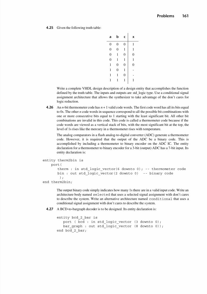
8/9/2019 VHDL for Engineers - Kenneth L. Short.pdf
http://slidepdf.com/reader/full/vhdl-for-engineers-kenneth-l-shortpdf 194/719
Problems 161
4.25 Given the following truth table:
Write a complete VHDL design description of a design entity that accomplishes the functiondefined by the truth table. The inputs and outputs are std_logic type. Use a conditional signalassignment architecture that allows the synthesizer to take advantage of the don’t cares forlogic reduction.
4.26 An n-bit thermometer code has n + 1 valid code words. The first code word has all its bits equalto 0s. The other n code words in sequence correspond to all the possible bit combinations withone or more consecutive bits equal to 1 starting with the least significant bit. All other bitcombinations are invalid in this code. This code is called a thermometer code because if thecode words are viewed as a vertical stack of bits, with the most significant bit at the top, thelevel of 1s rises like the mercury in a thermometer rises with temperature.
The analog comparators in a flash analog-to-digital converter (ADC) generate a thermometercode. However, it is required that the output of the ADC be a binary code. This isaccomplished by including a thermometer to binary encoder on the ADC IC. The entity
declaration for a thermometer to binary encoder for a 3-bit (output) ADC has a 7-bit input. Itsentity declaration is:
entity therm2bin is port( therm : in std_logic_vector(6 downto 0); -- thermometer code bin : out std_logic_vector(2 downto 0) -- binary code );end therm2bin;
The output binary code simply indicates how many 1s there are in a valid input code. Write anarchitecture body named selected that uses a selected signal assignment with don’t cares
to describe the system. Write an alternative architecture named conditional that uses aconditional signal assignment with don’t cares to describe the system.
4.27 A BCD-to-bargraph decoder is to be designed. Its entity declaration is:
entity bcd_2_bar is port ( bcd : in std_logic_vector (3 downto 0); bar_graph : out std_logic_vector (8 downto 0));end bcd_2_bar;
a b c x
0 0 0 1
0 0 1 10 1 0 0
0 1 1 1
1 0 0 0
1 0 1 -
1 1 0 -
1 1 1 1

8/9/2019 VHDL for Engineers - Kenneth L. Short.pdf
http://slidepdf.com/reader/full/vhdl-for-engineers-kenneth-l-shortpdf 195/719
162 Chapter 4 Dataflow Style Combinational Design
The inputs represent a binary value between 0 and 9. There are nine outputs. Each output drivesan LED. When an output is 0, its associated LED is ON. When it is 1, its associated LED isOFF. The LEDs are stacked in a vertical bar. The top LED is driven by bargraph(8) andthe bottom LED is driven by bargraph(0).
When the input combination is 0000, all the LEDs are OFF. As the input is stepped from 0001
to 1001, the next higher LED turns ON in sequence, from the bottom to the top. When the inputis 1001 all the LEDs are ON. As a result, the number of LEDs that are ON indicate the valueof the BCD input.
Input values from 1010 to 1111 are invalid. If it were possible in an application that thesenumbers could actually occur as input values, you could simply leave all the LEDs ON for theseinput combinations. If it was known that none of these inputs would occur, the decoder’s outputscould be specified as don’t cares for these input combinations. Thus, the two different designs.(a) Write a description of the converter using a selected signal assignment. Have all outputs
1s for the six invalid input codes.(b) Write a description of the converter using selected signal assignments. Assign all outputs
don’t care values for the six invalid input codes.
(c) Write a description of the converter using a conditional signal assignment. Have all outputs1s for the six invalid input codes.
(d) Write a description of the converter using conditional signal assignments. Assign alloutputs don’t care values for the five invalid input codes.
(e) Synthesize the designs and compare the amount of logic required for each implementation.
4.28 A 74HC139 contains two 1-out-of-4 decoders in a single MSI circuit. The truth table for asingle 1-out-of 4 decoder is given below.
As can be seen from the truth table, the 1-out-of-4 decoder has three inputs and four outputs.Inputs B and A select which output is asserted when the decoder is enabled. The decoder isenabled when the enable input G is a 0. Since VHDL does not allow overbars in identifiers, a
common way of naming a signal that is active-low is to attach the suffix_bar to the signal name.Accordingly, you will use g_bar in your VHDL code to represent G.(a) Write an entity declaration for the entity decode, which is a single 1-out-of-4 decoder
whose truth table is given above.(b) Write an architecture in the dataflow style for the entity decode. Use only conditional
signal assignment statements.
InputsOutputs
GSelect
B A Y0 Y1 Y2 Y3
1 X X 1 1 1 1
0 0 0 0 1 1 1
0 0 1 1 0 1 1
0 1 0 1 1 0 1
0 1 1 1 1 1 0

8/9/2019 VHDL for Engineers - Kenneth L. Short.pdf
http://slidepdf.com/reader/full/vhdl-for-engineers-kenneth-l-shortpdf 196/719
Problems 163
4.29 Modify the BCD to seven-segment decoder in Listing 4.8.2, to create a hexadecimal to seven-segment decoder named hex_7seg. For this decoder, input dcba is interpreted as a 4-bithexadecimal code. Output seg displays the value of the hexadecimal input on the seven-segment LED display.
4.30 Given the entity declaration for a BCD to seven-segment decoder in Listing 4.8.2, where eachoutput that drives a segment is a '0' to turn the segment ON and a '1' to turn the segment OFF.(a) Write a design description whose architecture uses a selected signal assignment to
implement the conversion function. Specify the outputs as don’t cares for non-BCD inputvalues, so that the synthesizer can produce the simplest logic.
(b) Write a design description whose architecture uses a table lookup to implement theconversion function. Specify the outputs as don’t cares for non-BCD input values so thatthe synthesizer can produce the simplest logic.
4.31 For the function specified by the truth table in Problem 4.25, write a complete description thatimplements the function using a table lookup. The architecture must allow the synthesizer totake advantage of the don’t care conditions in implementing the function.
4.32 Write an alternative architecture that uses table lookup to describe the BCD to seven-segmentdecoder of Listing 4.8.2. The architecture must allow the synthesizer to take advantage of thedon’t care conditions in implementing the function.
4.33 Given the following truth table:
(a) Write a complete design description for a design entity named two_out_tt thatimplements the function described by the truth table above. The architecture body mustuse only a table lookup to implement the function. The name of the table is outputs andits type is table.
(b) Draw Karnaugh maps and determine how the synthesizer would assign 0s or 1s to the don’tcare output values to synthesize minimal SOP logic for the outputs.
4.34 Design a 2421 code to BCD converter. The input to the converter is the std_logic_vectorc2421 (3 downto 0). The input vector represents a 2421 code for a decimal digit between 0and 9. The converter’s output is the std_logic_vector BCD (3 downto 0). The output vectorrepresents the BCD code for the decimal digit indicated by the 2421 code.
a b c x y
0 0 0 1 0
0 0 1 0 -
0 1 0 1 0
0 1 1 0 -1 0 0 0 0
1 0 1 - 1
1 1 0 0 0
1 1 1 1 1

8/9/2019 VHDL for Engineers - Kenneth L. Short.pdf
http://slidepdf.com/reader/full/vhdl-for-engineers-kenneth-l-shortpdf 197/719

8/9/2019 VHDL for Engineers - Kenneth L. Short.pdf
http://slidepdf.com/reader/full/vhdl-for-engineers-kenneth-l-shortpdf 198/719
165
Chapter 5
Behavioral Style Combinational Design
A behavioral style architecture uses algorithms in the form of sequential programs todescribe a system. These sequential programs are called processes. Unlike dataflowor structural styles, a behavioral style description does not imply a particularhardware implementation. It simply tells how the system is to behave.
The statement part of a behavioral style architecture consists of one or moreprocess statements. Each process statement is, in its entirety, a concurrent statement.Accordingly, processes can execute simultaneously.
Processes communicate with each other, and with other concurrent statements,using signals. This communication is analogous to the way components in a struc-tural description communicate.
Statements inside a process are sequential statements. They are executed insequence and their order is critical to their effect. Sequential statements are intro-duced in this chapter and used to describe combinational systems. Starting inChapter 8, sequential statements are also used to describe sequential systems.
Variables are also introduced in this chapter. They are used to store local datainside a process. A variable is declared inside a process or subprogram and is onlyvisible in that process or subprogram. Variables in VHDL are similar to those inconventional programming languages. A variable’s value is changed using a variableassignment statement.
5 .1 B EH AV IO RA L ST YL E ARC HI TE CT UR E
Recall that the statement part of an architecture body can contain only concurrentstatements. A behavioral style architecture contains one or more processes. Each

8/9/2019 VHDL for Engineers - Kenneth L. Short.pdf
http://slidepdf.com/reader/full/vhdl-for-engineers-kenneth-l-shortpdf 199/719
166 Chapter 5 Behavioral Style Combinational Design
process is a concurrent statement, so processes are able to execute simultaneously. Atwo-process version of the half adder is shown in Listing 5.1.1.
This half adder consists of two processes, labeled p1 and p2. Each process startswith the keyword process. Following keyword process is a sensitivity list (inparentheses). Process p1 has two signals, a and b, in its sensitivity list. This process
executes whenever there is an event on either of these signals. Thus, this process issensitive to a and b.
Process p1 contains a single signal assignment statement:
sum <= a xor b;
Sequential SignalAssignmentStatements
This same statement appeared in some previous dataflow versions of the half adder.However, because it then appeared by itself in the statement part of an architecturebody, it was a concurrent signal assignment statement. In Listing 5.1.1, because thesame signal assignment statement appears within a process, it is a sequential signalassignment statement. Thus, whether a signal assignment statement is concurrent orsequential depends on its location (context).
LISTING 5.1.1Half adder using two processes.
library ieee;use ieee.std_logic_1164.all;
entity half_adder is
port (a, b : in std_logic;
sum, carry_out : out std_logic);end half_adder;
architecture two_processes of half_adder is
begin
p1: process (a,b) begin
sum <= a xor b; -- sequential signal assignment end process p1;
p2: process (a,b)
begin carry_out <= a and b; -- sequential signal assignment end process p2;
end two_processes;

8/9/2019 VHDL for Engineers - Kenneth L. Short.pdf
http://slidepdf.com/reader/full/vhdl-for-engineers-kenneth-l-shortpdf 200/719
Section 5.1 Behavioral Style Architecture 167
In this example, processes p1 and p2 are independent of each other because each
is sensitive only to input port signals and not to any signal assigned a value by theother process. Because they are independent, they do not need to communicate.
ProcessCommunication
A block diagram of a full adder described by three separate communicatingprocesses is shown in Figure 5.1.1. These processes communicate using signals s1,s2, and s3. Process communication using signals is similar to the way componentsin a structural description communicate (are connected). The interprocess communi-cation in this example is identical to that of the half-adder and OR components in thestructural full-adder architecture in Figure 2.9.1.
A behavioral description of this full adder appears in Listing 5.1.2.
LISTING 5.1.2Full-adder behavioral description using communicating processes.
library ieee;use ieee.std_logic_1164.all;
entity full_adder is
port (a, b, carry_in : in std_logic; sum, carry_out: out std_logic);end full_adder;
architecture processes of full_adder is
signal s1, s2, s3 : std_logic; -- Signals to interconnect processes(Cont.)
FIGURE 5.1.1
Three processes communicating, using signals, to implement a full adder.
ha1
or1
a
b
a
b
s1
s2
sum
carry_out ha2
a
b
sum
carry_out
a
b
or_out
carry_in
sum
carry_outs3

8/9/2019 VHDL for Engineers - Kenneth L. Short.pdf
http://slidepdf.com/reader/full/vhdl-for-engineers-kenneth-l-shortpdf 201/719
168 Chapter 5 Behavioral Style Combinational Design
LISTING 5.1.2 (Cont.)
begin
-- Each process is a concurrent statement
ha1: process (a, b) -- ha1 process begin
if a = '1' then
s1 <= not b; s2 <= b; else
s1 <= b; s2 <= '0'; end if; end process ha1;
ha2: process (s1, carry_in) -- ha2 process
begin if s1 = '1' then
sum <= not carry_in; s3 <= carry_in; else
sum <= carry_in; s3 <= '0'; end if; end process ha2;
or1: process (s3, s2) -- or1 process begin
if (s3 = '1') or (s2 = '1') then
carry_out <= '1'; else
carry_out <= '0'; end if; end process or1;
end processes
Processes ha1 and ha2 are algorithms for half-adder functions. In fact, they are theidentical algorithm operating on different sets of signals. Process or1 is an algorithmfor the OR function. Signals s1, s2, and s3 are declared in the architecture body’sdeclarative part.

8/9/2019 VHDL for Engineers - Kenneth L. Short.pdf
http://slidepdf.com/reader/full/vhdl-for-engineers-kenneth-l-shortpdf 202/719
Section 5.2 Process Statement 169
5 . 2 P RO C E S S S TAT EME N T
A process statement may represent the behavior of all or some portion of a design. A process statement is a concurrent statement that itself is comprised of sequential
statements. Included in these sequential statements can be statements that callsubprograms. The simplified syntax for a process statement is given in Figure 5.2.1.
Following the keyword process is an optional sensitivity list, which is followedby the optional keyword is.
The declarative part of a process consists of zero or more declarations. Amongother items, variables can be declared here. No signals can be declared in a process.
The statement part of a process follows the keyword begin and consists of zeroor more sequential statements. Sequential statements are executed in sequence andtheir order is critical. The order of the sequential statements affects what logic issynthesized. The sequential statement part of a process is terminated by thekeywords end process.
Sensitivity List Since the sensitivity list is optional, there are two kinds of processes: those with asensitivity list and those without. Processes used to synthesize logic typically havesensitivity lists.
A sensitivity list is a list of signals to which a process is sensitive. Signals in thesensitivity list may be signals declared in the enclosing architecture and/or ports of the associated entity declaration. The order of signals in a sensitivity list is notimportant.
Recall that an event was defined in Chapter 1 as a change in a signal’s value.Whenever there is an event on a signal in its sensitivity list, the process is executed.
If a signal name that denotes a composite type signal appears in a sensitivity list, anevent on any element of the composite is an event on the composite signal, causingthe process to execute.
process_statement ;;=
[ process _label : ]
process [ ( sensitivity_list ) ] [ is ]
{ process_declarative_item } -- process declarative part
begin
{ sequential_statement } -- process statement part
end process [ process _label ] ;
FIGURE 5.2.1
Simplified syntax for a process statement.

8/9/2019 VHDL for Engineers - Kenneth L. Short.pdf
http://slidepdf.com/reader/full/vhdl-for-engineers-kenneth-l-shortpdf 203/719
170 Chapter 5 Behavioral Style Combinational Design
A process with a sensitivity list must not contain any wait statements. A processwithout a sensitivity list must contain at least one wait statement, or its simulationwill never end.
Process Execution A process can be viewed as an infinite loop whose execution is repeatedly suspendedand resumed. The sequential statements in a process are executed from the first to thelast, then back to the first. A process continues to execute its sequential statementsuntil the process is suspended.
Suspending aProcess That Hasa Sensitivity List
A process that has a sensitivity list automatically suspends after the last statement inthe process is executed. When there is a subsequent event on a signal in its sensitivitylist, the process resumes execution, starting with the first statement, and executes toits last statement. Since a process with a sensitivity list cannot contain any wait state-ments, any procedure that it calls cannot contain a wait statement.
Suspending aProcess That HasNo Sensitivity List
A process that does not contain a sensitivity list suspends when it encounters a waitstatement. The process resumes execution when the wait statement’s conditions aresatisfied. For now our focus is solely on processes that have sensitivity lists. Waitstatements and processes containing them are discussed in detail in Chapter 7.
Using a Processto DescribeCombinationalLogic
Processes can be used to describe combinational or sequential systems. Two require-ments for a process to synthesize to a combinational system are:
1. The process’s sensitivity list must contain all signals read in the process.
2. A signal or variable assigned a value in a process must be assigned a value inall possible executions of the process.
5 . 3 S EQU EN TI AL S TAT EME N T S
Sequential statements are executed one after another. They can appear only inside of a process or a subprogram and are used to describe algorithms. In this chapter, thediscussion is limited to use of sequential statements in processes. Sequential state-ments in subprograms are discussed in Chapter 12. VHDL’s sequential statementsare listed in Table 5.3.1.
Sequential signal assignment statements were introduced earlier in this chapter. Amore detailed discussion of signal assignment statements is presented in Chapter 6,where we look at additional variations of the signal assignment statement andexamine in detail just when a new value is assigned to a signal.
Variables are introduced in Section 5.7, near the end of this chapter. Variableassignments statements are used to assign values to variables and are discussed inthat section.

8/9/2019 VHDL for Engineers - Kenneth L. Short.pdf
http://slidepdf.com/reader/full/vhdl-for-engineers-kenneth-l-shortpdf 204/719
Section 5.4 Case Statement 171
Wait, assertion, and report statements are considered in Chapter 7 in terms of theiruse in testbenches. Wait statements can also be used to synthesize storage elementsas described in Chapter 8.
Procedure call statements and return statements are discussed along with subpro-grams in Chapter 12.
Sequential Control
Statements
The remaining sequential statements in Table 5.3.1 are control statements. Control
statements select between alternative statement execution paths. Control statementsare introduced in this chapter, along with examples of their use in describing combi-national systems.
5 . 4 C A SE S TA T E ME NT
The case statement and the if statement both allow us to select one sequence of state-ments for execution from a number of alternative sequences.
Use of a case statement is appropriate when the selection can be based on thevalue of a single expression.
The case statement’s simplified syntax is given in Figure 5.4.1.When used to assign a value to a single signal, a sequential case statement is
essentially equivalent to a concurrent selected signal assignment statement. Theselected signal assignment statement is often referred to as a shorthand version of such a case statement.
Table 5.3.1VHDL’s sequential statements.
Sequential Statements
signal assignment
variable assignmentwaitassertionreportprocedure callreturncasenullifloopnextexit

8/9/2019 VHDL for Engineers - Kenneth L. Short.pdf
http://slidepdf.com/reader/full/vhdl-for-engineers-kenneth-l-shortpdf 205/719
172 Chapter 5 Behavioral Style Combinational Design
Case Expression The expression following the keywordcase is called the case expression (or selectorexpression). This expression must be of a discrete type or of a one-dimensionalcharacter array type.
Case Choices The choices specify for which values of the case expression a particular branch isexecuted. Each branch contains an alternative sequence of statements. The choicesmust be mutually exclusive locally static values of the case expression. Locally staticmeans that the choice values must be determinable when the architecture containingthe case statement is compiled. This restriction rules out the use of a variable inspecifying a choice.
One and only one choice in a case statement must match the value of the caseexpression. Accordingly, in addition to the choices being mutually exclusive, exactlyone choice must appear for every possible value of the case expression. That is, the
choices must be exhaustive.
Listing Choices A list of choices can be associated with a single branch by separating each choice inthe list using the vertical bar ( | ) symbol.
Others Choice ina Case Statement
If the set of choices does not enumerate every possible value of the case expressiontype, then the last when choices clause must be an others choice.
The others choice handles all possible values of the case expression notexplicitly listed in previous choices. Only one branch may have an others choiceand, if it is included, it must be the only choice of the last branch in the case statement.
A branch with an others choice can still be included, even if all possible valuesof the case expression have been covered by previous choices. In this situation, thebranch associated with the others choice will never be selected.
case_statement ::=
case expression is
when choices => sequence_of_statements
{ when choices => sequence_of_statements }
end case [ case_label ] ;
choices ::= choice { | choice }
choice ::= simple_expression | discrete_range | element _simple_name | others
FIGURE 5.4.1
Simplified syntax for a case statement.

8/9/2019 VHDL for Engineers - Kenneth L. Short.pdf
http://slidepdf.com/reader/full/vhdl-for-engineers-kenneth-l-shortpdf 206/719
Section 5.4 Case Statement 173
LISTING 5.4.1A two-input XOR using a case statement.
library ieee;use ieee.std_logic_1164.all;
entity xor_2 is port ( a, b : in std_logic; c : out std_logic);end xor_2;
architecture bhvxor2c of xor_2 is
begin
process (a, b) begin
case std_logic_vector'(a, b) is
when "01" => c <= '1';
when "10" => c <= '1'; when others => c <= '0'; end case; end process;end bhvxor2c;
Others Choice andDon’t Care OutputValues
For a combinational design that has input combinations for which we wish to assigndon’t care output values, the others choice can be used to select a sequence of statements that make the don’t care output assignments.
Case StatementExamples
In Listing 5.4.1 a two-input exclusive-OR function is described using a casestatement.
In this description, the case expression is a std_logic_vector aggregate of theentity’s inputs. The first two branches specify choices that are values of the inputsthat cause the XOR function to be a '1'. The others choice handles all the otherpossible values of the aggregate. For these values, the output is assigned a valueof '0'.
By taking advantage of the fact that we can specify more than one choice in achoice list by using the | symbol, the case statement in Listing 5.4.1 can be writtenmore concisely as:
case tmp is
when "01" | "10" => c <= '1'; when others => c <= '0';end case;
A 2-to-4 decoder is described using a case statement in Listing 5.4.2.
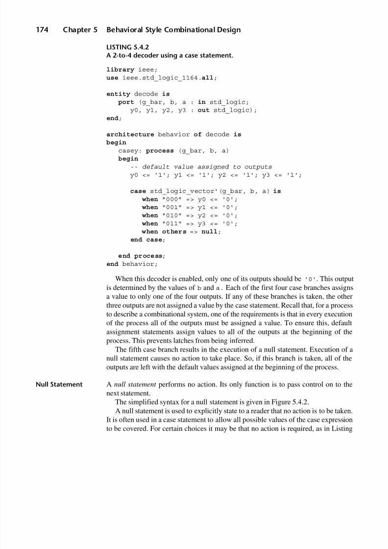
8/9/2019 VHDL for Engineers - Kenneth L. Short.pdf
http://slidepdf.com/reader/full/vhdl-for-engineers-kenneth-l-shortpdf 207/719
174 Chapter 5 Behavioral Style Combinational Design
LISTING 5.4.2A 2-to-4 decoder using a case statement.
library ieee;use ieee.std_logic_1164.all;
entity decode is port (g_bar, b, a : in std_logic; y0, y1, y2, y3 : out std_logic);end;
architecture behavior of decode is
begin
casey: process (g_bar, b, a) begin
-- default value assigned to outputs y0 <= '1'; y1 <= '1'; y2 <= '1'; y3 <= '1';
case std_logic_vector'(g_bar, b, a) is
when "000" => y0 <= '0'; when "001" => y1 <= '0'; when "010" => y2 <= '0'; when "011" => y3 <= '0'; when others => null; end case;
end process;end behavior;
When this decoder is enabled, only one of its outputs should be '0'. This outputis determined by the values of b and a. Each of the first four case branches assignsa value to only one of the four outputs. If any of these branches is taken, the otherthree outputs are not assigned a value by the case statement. Recall that, for a processto describe a combinational system, one of the requirements is that in every executionof the process all of the outputs must be assigned a value. To ensure this, defaultassignment statements assign values to all of the outputs at the beginning of theprocess. This prevents latches from being inferred.
The fifth case branch results in the execution of a null statement. Execution of anull statement causes no action to take place. So, if this branch is taken, all of the
outputs are left with the default values assigned at the beginning of the process.
Null Statement A null statement performs no action. Its only function is to pass control on to thenext statement.
The simplified syntax for a null statement is given in Figure 5.4.2.A null statement is used to explicitly state to a reader that no action is to be taken.
It is often used in a case statement to allow all possible values of the case expressionto be covered. For certain choices it may be that no action is required, as in Listing

8/9/2019 VHDL for Engineers - Kenneth L. Short.pdf
http://slidepdf.com/reader/full/vhdl-for-engineers-kenneth-l-shortpdf 208/719
Section 5.4 Case Statement 175
5.4.2. Use of the null statement makes our intentions clearer than simply leaving thatbranch void of any statements.
Example of a74F539 DecoderEquivalent
A 74F539 is a dual 2-to-4 decoder IC with three-state outputs. The truth table for thisdecoder is given in Table 5.4.1.
The 74F539 has three more control inputs than the previously considered 2-to-4decoders. If the output enable input OE is a 1, all outputs are in their high-impedancestates. If enable input E is a 1, no output is selected and all outputs have the value of the polarity input P. When both OE and E are 0s, the output selected by inputs A1 and
A0 has the value P, and all other outputs have the value P.Since the 74F539 is an obsolete part, we could design our own equivalent andimplement it in a PLD. While this decoder’s functionality is relatively complex, itsVHDL description is very concisely written using a case statement, Listing 5.4.3.
Inputs A1 and A0 are declared as the two-element std_logic_vectora. Outputs O3 toO0 are declared as the four-element vector o. The process assigns a default value of pto all outputs. This is accomplished by creating an aggregate of four copies of p. Thisaggregate does not need to be type qualified, because the compiler can determine fromthe context (the aggregate is assigned to std_logic_vector o) that it is typestd_logic_vector. A case statement is then used to assign a value to the output vectorbased on the values of oe_bar and e_bar and, in the case of the first branch, vectora.
null_statement ::=
null ;
FIGURE 5.4.2
Simplified syntax for a null statement.
Table 5.4.1Truth table for one half of a 74F539 dual 2-to-4 decoder.
FunctionInputs Outputs
OE E A1 A0 O0 O1 O2 O3
High impedance 1 – – – Z Z Z Z
Disable 0 1 – – On = P
Active High Output (P = 0) 0 0 0 0 1 0 0 0
0 0 0 1 0 1 0 0
0 0 1 0 0 0 1 0
0 0 1 1 0 0 0 1
Active Low Output (P = 1) 0 0 0 0 0 1 1 1
0 0 0 1 1 0 1 1
0 0 1 0 1 1 0 1
0 0 1 1 1 1 1 0

8/9/2019 VHDL for Engineers - Kenneth L. Short.pdf
http://slidepdf.com/reader/full/vhdl-for-engineers-kenneth-l-shortpdf 209/719
176 Chapter 5 Behavioral Style Combinational Design
LISTING 5.4.3Description of one half of a 74F359 dual 2-to-4 decoder.
library ieee;use ieee.std_logic_1164.all;use ieee.numeric_std.all;
entity ic74f539 is
port (a : in std_logic_vector(1 downto 0); -- address (select) inputsp : in std_logic; -- polarity inpute_bar : in std_logic; -- enable inputoe_bar : in std_logic; -- output enable inputo : out std_logic_vector(3 downto 0) -- outputs);
end ic74f539;
architecture behav_case of ic74f539 isbegin
process(a, p, oe_bar, e_bar)begin
o <= (p,p,p,p);case std_logic_vector'(oe_bar, e_bar) is
when "00" => o( to_integer(unsigned(a))) <= not p; when "01" => null; when others => o <= "ZZZZ";
end case;end process;
end behav_case;
5 . 5 I F ST AT E ME N T
An if statement selects one or none of its alternative sequences of statements forexecution, depending on the value of each branch’s condition. It establishes apriority in the determination of which sequence of statements is executed. An if statement has the simplified syntax given in Figure 5.5.1.
When used to assign a value to a single signal, a sequential if statement is essen-
tially equivalent to a concurrent conditional signal assignment statement. The condi-tional signal assignment statement is often referred to as a shorthand version of suchan if statement.
If StatementEvaluation
If the first condition in an if statement evaluates true, the sequence of statementsfollowing the first then is executed and the construct is terminated. If the firstcondition is not true, and an elsif clause is included, the condition associated with the

8/9/2019 VHDL for Engineers - Kenneth L. Short.pdf
http://slidepdf.com/reader/full/vhdl-for-engineers-kenneth-l-shortpdf 210/719
Section 5.5 If Statement 177
first elsif is tested. If this condition is true, the sequence of statements followingthe first elsif is executed and the construct is terminated.
Since the elsif clause in the syntax definition is enclosed in curly brackets, zero,
one, or a multiple number of elsif clauses may appear in the construct. The conditionassociated with each elsif clause is evaluated in succession until one evaluates true.The sequence of statements associated with the first elsif clause that evaluates true isthen executed and the construct is terminated.
If none of the elsif clauses evaluate true and an else clause is included, thesequence of statements following the else is executed and the construct isterminated.
If none of the conditions in the if statement evaluate true and there is no elseclause, then none of the included sequences of sequential statements is executed.
Common errors made when first writing if statements are to write elsif as twowords (else if) or to write end if as a single word (endif).
If StatementExamples
A two-input XOR gate is described in Listing 5.5.1 using an if statement. Thecondition associated with the if clause is the condition that causes the output to be'1'. Accordingly, the sequential statement following then assigns '1' to c. Theelse clause is included to handle all other input combinations. It assigns the value of '0' to c.
LISTING 5.5.1XOR gate described using an if statement with an else clause.
library ieee;use ieee.std_logic_1164.all;
entity xor_2 is
port ( a, b : in std_logic; c : out std_logic);end xor_2;
(Cont.)
if_statement ::=
if condition then
sequence_of_statements
{ elsif condition then
sequence_of_statements }
[ else
sequence_of_statements ]
end if [ if _label ] ;
FIGURE 5.5.1
Simplified syntax for an if statement.

8/9/2019 VHDL for Engineers - Kenneth L. Short.pdf
http://slidepdf.com/reader/full/vhdl-for-engineers-kenneth-l-shortpdf 211/719
178 Chapter 5 Behavioral Style Combinational Design
LISTING 5.5.1 (Cont.)
architecture bhvxor2i of xor_2 is
begin
process ( a, b) begin
if a /= b then
c <= '1'; else
c <= '0'; -- default end if; end process;end bhvxor2i;
Adding default assignments at the beginning of a process eliminates the need foran else clause when describing combinational circuits using an if statement. In
Listing 5.5.2 the default assignment to c is made at the beginning of the process andthe else clause is eliminated.
Since there is no limitation on the kind of sequential statements in an if statement,if statements can be nested. In Listing 5.5.3, a 2-to-4 decoder is described usingnested if statements.
LISTING 5.5.2XOR gate described using a default signal assignment and an if without an else.
library ieee;use ieee.std_logic_1164.all;
entity xor_2 is
port ( a, b : in std_logic; c : out std_logic);end xor_2;
architecture bhvxor2id of xor_2 is
begin
process ( a, b) begin
c <= '0'; -- default
if a /= b then
c <= '1';
end if; end process;end bhvxor2id;

8/9/2019 VHDL for Engineers - Kenneth L. Short.pdf
http://slidepdf.com/reader/full/vhdl-for-engineers-kenneth-l-shortpdf 212/719
Section 5.5 If Statement 179
LISTING 5.5.3A 2-to-4 decoder using nested if statements.
library ieee;use ieee.std_logic_1164.all;
entity decode is port (g_bar, b, a : in std_logic; y0, y1, y2, y3 : out std_logic);end;
architecture behavior of decode is
begin
iffy: process (g_bar, b, a) begin
y0 <= '1';-- default output values
y1 <= '1'; y2 <= '1'; y3 <= '1';
if (g_bar ='0') then
if ((b ='0') and (a = '0')) then
y0 <= '0'; elsif ((b ='0') and (a = '1')) then
y1 <= '0'; elsif ((b ='1') and (a = '0')) then
y2 <= '0'; elsif ((b ='1') and (a = '1')) then
y3 <= '0'; end if; end if; end process;end behavior;
An example of a behavioral description of a 4-bit magnitude comparator describedusing multiple processes, each consisting of a single if statement, is shown inListing 5.5.4. This comparator is functionally equivalent to the one in Listing 4.5.1.
LISTING 5.5.4
A 4-bit magnitude comparator using processes containing if statements.
library ieee;use ieee.std_logic_1164.all;
entity mag_comp is
port ( p, q : in std_logic_vector (3 downto 0);(Cont.)

8/9/2019 VHDL for Engineers - Kenneth L. Short.pdf
http://slidepdf.com/reader/full/vhdl-for-engineers-kenneth-l-shortpdf 213/719
180 Chapter 5 Behavioral Style Combinational Design
LISTING 5.5.4 (Cont.)
p_gt_q_bar, p_eq_q_bar, p_lt_q_bar : out std_logic);end mag_comp;
architecture behavior of mag_comp is
begin
gt: process (p, q) begin
if p > q then
p_gt_q_bar <= '0'; else
p_gt_q_bar <= '1'; end if; end process gt;
lt: process (p, q)
begin if p < q then
p_lt_q_bar <= '0'; else
p_lt_q_bar <= '1'; end if; end process lt;
eq: process (p, q) begin
if p = q then
p_eq_q_bar <= '0'; else
p_eq_q_bar <= '1'; end if; end process eq;
end behavior;
This architecture has three independent processes. Each process computes one of the three outputs. The condition in each if statement uses a relational operator tomake the comparison.
Case Statementversus If Statement
Case and if statements are similar in that they both allow us to select betweenexecution of alternative sequences of sequential statements. Their difference is inhow the selection is made.
A case statement evaluates a single case expression and executes the sequence of statements associated with the choice that matches the value of the case expression.

8/9/2019 VHDL for Engineers - Kenneth L. Short.pdf
http://slidepdf.com/reader/full/vhdl-for-engineers-kenneth-l-shortpdf 214/719
Section 5.6 Loop Statement 181
An if statement evaluates one or more conditions in succession and executes thesequence of statements associated with the first condition that evaluates true. An if statement provides inherent priority.
Since an if statement is capable of evaluating multiple arbitrarily complex condi-tions to make a selection, it is more flexible than a case statement.
5 . 6 L OO P ST AT E M E N T
A loop statement contains a sequence of sequential statements that can be repeatedlyexecuted, zero or more times. It has the simplified syntax shown in Figure 5.6.1.
Execution of a loop continues until the loop is terminated as a result of any of thefollowing:
• Completion of its iteration scheme• Execution of an exit statement
• Execution of a next statement that specifies a label outside of the loop
• Execution of a return statement
A return statement can appear inside a loop only if the loop is in a subprogram.
Infinite Loop As indicated in Figure 5.6.1, the iteration scheme is optional. A loop statementwithout an iteration scheme is an infinite loop, one whose sequence of statements isexecuted endlessly. An infinite loop cannot be synthesized.
Iteration Schemes There are two possible iteration schemes, resulting in two kinds of loops: for loopsand while loops. For loops are synthesizable, but while loops are not. Although notsynthesizable, while loops are useful in testbenches.
loop_statement ::=
[ loop_label:]
[ iteration_scheme ] loop
sequence_of_statements
end loop [ loop_label ] ;
iteration_scheme ::= for identifier in discrete_range | while condition
discrete_range ::= discrete_subtype_indication | range
FIGURE 5.6.1
Simplified syntax for a loop statement.

8/9/2019 VHDL for Engineers - Kenneth L. Short.pdf
http://slidepdf.com/reader/full/vhdl-for-engineers-kenneth-l-shortpdf 215/719
182 Chapter 5 Behavioral Style Combinational Design
For Loop Substituting the for iteration scheme into the syntax of Figure 5.6.1 gives:
[loop_label:] for identifier in range loop
sequence_of_statementsend loop [loop_label];
In a for loop, the identifier following keyword for serves as an implicit declarationof a loop parameter with the specified name. Thus, we do not need to explicitlydeclare a loop parameter. The loop parameter’s type is the base type of the discreterange. The loop parameter only exists while the loop is being executed, and is notvisible outside of the loop.
Within the sequence of sequential statements, the loop parameter is treated as aconstant. Thus, it can be read by statements within the loop, but it cannot be written.
For Loop Execution The discrete range specifies how many iterations of the loop are to occur. To executea for loop, the discrete range is first evaluated. If the discrete range is null, the loop’s
execution is complete and the sequence of statements in the loop is not executed.If the discrete range is not null, the instructions in the loop are normally executed
once for each value of the discrete range. However, if a next, exit, or return statementappears in the loop, it can cause fewer iterations of the loop to occur before it isterminated.
Prior to each loop iteration, the corresponding value of the discrete range isassigned to the loop parameter. Values from the discrete range are assigned to theloop parameter in left-to-right order. After the loop has been executed the specifiednumber of times, the iteration scheme is complete and the loop is terminated.
While Loop Substituting the while iteration scheme into the syntax of Figure 5.6.1 gives:
[loop_label:] while condition loop
sequence_of_statementsend loop [loop_label];
The condition of a while loop is evaluated before each iteration of the loop, includingthe first iteration. If the condition is true, the sequence of statements in the loop isexecuted. If false, the iteration scheme is complete and the loop is terminated. Thecondition is not tested during the execution of the sequence of statements in the loop.
With a while loop, we must ensure that statements inside the loop will eventually
cause the loop’s condition to evaluate false or cause an exit statement or returnstatement to be executed to terminate the loop. Otherwise, the loop is infinite.
Next and Exit Statements
Next and exit statements are used only inside of loops. They are used to terminate theexecution of a single iteration of a loop or to terminate an entire loop, respectively.

8/9/2019 VHDL for Engineers - Kenneth L. Short.pdf
http://slidepdf.com/reader/full/vhdl-for-engineers-kenneth-l-shortpdf 216/719

8/9/2019 VHDL for Engineers - Kenneth L. Short.pdf
http://slidepdf.com/reader/full/vhdl-for-engineers-kenneth-l-shortpdf 217/719
184 Chapter 5 Behavioral Style Combinational Design
LISTING 5.6.1A 4-bit magnitude comparator described using a for loop.
library ieee;use ieee.std_logic_1164.all;
entity mag_comp is port ( p, q : in std_logic_vector (3 downto 0); p_gt_q_bar, p_eq_q_bar, p_lt_q_bar : out std_logic);end mag_comp;
architecture behavior of mag_comp is
begin
comp: process (p, q) begin
p_gt_q_bar <= '1'; --defaults
p_eq_q_bar <= '1'; p_lt_q_bar <= '1';
for i in 3 downto 0 loop
if ((p(i) = '1') and (q(i) = '0')) then
p_gt_q_bar <= '0'; exit; elsif((p(i) = '0') and (q(i) = '1')) then
p_lt_q_bar <= '0'; exit; elsif i = 0 then
p_eq_q_bar <= '0'; end if; end loop;
end process comp;end behavior;
The process first sets all the outputs to '1's, then uses a for loop to determinewhich output to make a '0'.
The range of the loop parameter i is from 3 down to 0. During each loop iteration,the if statement compares two corresponding elements of p and q to determine which
vector is greater. As soon as the determination can be made, the loop is exited.In each pass through the loop, the if clause determines whether p(i) is a '1' and
q(i) is a '0'. If this condition is true, output p_gt_q_bar is assigned '0', and theexit statement terminates the loop.
If the previous condition does not evaluate true, the first elsif clause determineswhether p(i) is a '0' and q(i) is a '1'. If this condition is true, outputp_lt_q_bar is assigned '0' and the exit statement terminates the loop.

8/9/2019 VHDL for Engineers - Kenneth L. Short.pdf
http://slidepdf.com/reader/full/vhdl-for-engineers-kenneth-l-shortpdf 218/719
Section 5.7 Variables 185
The last elsif determines whether loop parameter i equals 0. This condition canbe true only on the fourth pass through the loop. If this condition is true, outputp_eq_q_bar is assigned '0', because all of the corresponding elements of the twovectors must have been equal to reach this point.
5 . 7 VA R IA B LE S
The four kinds of VHDL objects were introduced in Chapter 3: signals, constants,variables, and files. Signals and constants have been used extensively in previousexamples. We now examine variables and use them in descriptions.
Normal Variablesand SharedVariables
There are two kinds of variables in VHDL, normal variables and shared variables.Shared variables can be accessed from multiple processes and are not synthesizable.Normal variables can only be accessed from a single process or subprogram and aresynthesizable. The subsequent discussions of variables in this book are limited tonormal variables.
StoringIntermediate Valuesin a Processor Subprogram
Variables are used to store intermediate values in a process or subprogram. Variablesmust be declared in the declarative part of the process or subprogram in which theyare used. A variable is local to the process or subprogram in which it is declared(visible only within that process or subprogram).
Variables in a process preserve their values between executions of the process.That is, between its suspension and reactivation. In contrast, variables in asubprogram do not preserve their values between executions of the subprogram.Variables in subprograms are discussed further in Chapter 12.
The syntax for a variable declaration is given in Figure 5.7.1.
Variable InitialValue
A variable can optionally be assigned an initial value when it is declared. Aninitial value is assigned by using the variable assignment symbol := . For example:
variable count : std_logic_vector (3 downto 0) := "0000";
This statement declares variable count and gives it an initial value of "0000".
Importantly, IEEE 1076.6 compliant synthesizers ignore initial values assigned to
variable_declaration ::=
[shared] variable identifier_list : subtype_indication [:= expression] ;
FIGURE 5.7.1
Syntax for a variable declaration.

8/9/2019 VHDL for Engineers - Kenneth L. Short.pdf
http://slidepdf.com/reader/full/vhdl-for-engineers-kenneth-l-shortpdf 219/719
186 Chapter 5 Behavioral Style Combinational Design
variables. Accordingly, in a description, if a variable requires an initial value, itshould be assigned by a separate variable assignment statement in the process orsubprogram that uses the variable.
Variable
AssignmentStatement
Variables are assigned values by using a variable assignment statement. To distin-guish assignments to variables from assignments to signals, two different assignmentsymbols are used. The symbol := is the variable assignment symbol. For example:
count := "0000";
assigns the value "0000" to the variable count.
VariableAssignments TakeEffect Immediately
When a variable is assigned a value, it takes that value immediately. This action isthe same as for a variable in a conventional programming language. However, it isdifferent from the situation for a signal. When a signal is assigned a value, theassigned value does not take effect immediately. When a signal is assigned a value ina process, the signal does not take the new value until after the process hassuspended. This characteristic of a signal has not been previously emphasized. It isconsidered in detail in Chapter 6.
It will also become more clear in Chapter 6 when use of a variable in a process ispreferable to use of a signal. However, as a general guideline, a variable is used tostore data within a process when the new value assigned to the variable is to be used(read) in the same execution of the process.
Variable and SignalDifferences
At this point, some of the obvious differences between a variable and a signal in aprocess can be stated.
• A variable used in a process must be declared inside the process. A signal usedin a process must be declared outside of the process (in the declarative part ofthe architecture or as a port in the associated entity declaration).
• A variable is only visible in the process in which it is declared. A signal isvisible to all processes in the architecture in which it is declared.
As an example of the use of variables, the magnitude comparator is described usingvariables in Listing 5.7.1.
LISTING 5.7.1A 4-bit magnitude comparator description using variables.
library ieee;use ieee.std_logic_1164.all;
entity mag_comp is
port ( p, q : in std_logic_vector (3 downto 0); p_gt_q_bar, p_eq_q_bar, p_lt_q_bar : out std_logic);end mag_comp;

8/9/2019 VHDL for Engineers - Kenneth L. Short.pdf
http://slidepdf.com/reader/full/vhdl-for-engineers-kenneth-l-shortpdf 220/719
Section 5.7 Variables 187
architecture vari of mag_comp is
begin
comp: process (p, q)
variable p_gt_q_bar_v, p_lt_q_bar_v, p_eq_q_bar_v : std_logic;
begin
p_gt_q_bar_v := '1'; -- default values p_lt_q_bar_v := '1'; p_eq_q_bar_v := '1';
for i in 3 downto 0 loop
if ((p(i) = '1') and (q(i) = '0')) then
p_gt_q_bar_v := '0'; exit;
elsif ((p(i) = '0') and (q(i) = '1')) then p_lt_q_bar_v := '0'; exit; end if; end loop;
if ((p_gt_q_bar_v = '1') and (p_lt_q_bar_v = '1')) then
p_eq_q_bar_v := '0'; end if;
p_gt_q_bar <= p_gt_q_bar_v; -- assign variable values to ports p_lt_q_bar <= p_lt_q_bar_v; p_eq_q_bar <= p_eq_q_bar_v;
end process comp;end vari;
In this description, the determination as to whether to assert p_eq_q_bar is madebased on the values of p_gt_q_bar and p_lt_q_bar determined during the sameexecution of the process. Variables are used to store intermediate values.
Variables p_gt_q_bar_v, p_lt_q_bar_v, and p_eq_q_bar_v are declared inthe declarative part of the process. In the statement part of the process these variables
are all given a default value of '1'. A loop is used to determine if eitherp_gt_q_bar_v or p_lt_q_bar_v should be asserted. If either of these variables isto be asserted, it is assigned a '0'. This assignment takes effect immediately.
After the loop is terminated, an if statement is used to determine whether variablep_eq_q_bar_v should be asserted. If either p_gt_q_bar_v or p_lt_q_bar_v
were assigned a value of '0' in an execution of the loop statement, that '0' isdetected in the execution of the if statement.

8/9/2019 VHDL for Engineers - Kenneth L. Short.pdf
http://slidepdf.com/reader/full/vhdl-for-engineers-kenneth-l-shortpdf 221/719
188 Chapter 5 Behavioral Style Combinational Design
Before the process ends, the values of the variables are assigned to the corre-sponding ports. This must be done inside the process because variables are notvisible outside of a process.
5 . 8 PA RIT Y D ETE C T OR EX AMP LE
A few examples of designs for a parity detector are given in this section. Theseexamples clarify some important concepts concerning variables and signals. Designentity parity takes a four-element std_logic_vector named din as its input and hasa single std_logic output oddp. Output oddp is asserted when the number of 1s inthe input vector is odd, otherwise it is unasserted.
DataflowDescription ofParity Detector
If we are aware that a four-input XOR gate detects odd parity for a 4-bit vector, thesimplest way to describe the parity detector is using a single concurrent signalassignment statement. A dataflow style description using this approach is given inListing 5.8.1.
A simulation of this design description results in the waveforms in Figure 5.8.1.The testbench sequences through all possible binary input combinations. Input
vector din is displayed as both a composite signal, whose value is expressed inhexadecimal, and in terms of its separate elements. The waveforms indicate that thedescription is functionally correct.
Synthesis of the design description in Listing 5.8.1 produces the hierarchical repre-sentation of the logic in Figure 5.8.2. The notation [3:0] represents a 4-bit bus. Thenotation [3] indicates bit 3 of the bus. As expected, the logic is a four-input XOR gate.
LISTING 5.8.1Dataflow design description of parity detector.
library ieee;use ieee.std_logic_1164.all;
entity parity is
port ( din: in std_logic_vector (3 downto 0); -- 4-bit input vector oddp: out std_logic -- asserted for odd parity
);end parity;
architecture dataflow of parity is
begin
oddp <= din(3) xor din(2) xor din(1) xor din(0);end dataflow;

8/9/2019 VHDL for Engineers - Kenneth L. Short.pdf
http://slidepdf.com/reader/full/vhdl-for-engineers-kenneth-l-shortpdf 222/719
Section 5.8 Parity Detector Example 189
Loop and Signal
Description ofParity Detector
In contrast to the dataflow approach, we might envision the function of the parity
detector in terms of an algorithm that examines each bit of the input vector one at atime and keeps track of whether the parity of all bits previously examined is odd.After the last bit has been examined, the parity of the entire vector is known.
An architecture using this iterative approach is given in Listing 5.8.2. The entitydeclaration for the parity detector remains the same.
In Listing 5.8.2, a loop is used to examine each bit of the input vector in turn,starting with the leftmost bit. A signal named odd is used to keep track of thecomputed parity. This signal is declared in the declarative part of the architecture.
In the process, signal odd is first assigned the value '0'. The loop is then entered.Each time through the loop, odd is assigned the XOR of the current value of odd and
the element of the input vector selected by the loop index. When the loop iscomplete, the value of signal odd is assigned to output port oddp.When the description in Listing 5.8.2 is simulated using the same testbench as
before, the waveforms in Figure 5.8.3 result.It is obvious from the waveforms that the output is incorrect. The value of oddp
remains 'U' for the entire simulation. The value 'U' is indicated in the waveform bythe dotted line halfway between the '0' and '1' logic levels.
FIGURE 5.8.1
Simulation of dataflow style parity detector.
FIGURE 5.8.2
Logic synthesized from the dataflow style parity detector description inListing 5.8.1.
[3:0]
[2]
[0]
[1]
[3]din[3:0]
oddp
oddp

8/9/2019 VHDL for Engineers - Kenneth L. Short.pdf
http://slidepdf.com/reader/full/vhdl-for-engineers-kenneth-l-shortpdf 223/719
190 Chapter 5 Behavioral Style Combinational Design
LISTING 5.8.2Architecture for parity detector written using a loop and a signal.
architecture behav_sig of parity is
signal odd : std_logic;begin
po: process (din) begin
odd <= '0'; for index in 3 downto 0 loop
odd <= odd xor din(index); end loop; end process; oddp <= odd;end behav_sig;
Before examining why this description failed, lets see what would have happened
if, because the design seemed so simple, we skipped simulation and went directly tosynthesis. Synthesis using the architecture in Listing 5.8.2 produces the logic inFigure 5.8.4.
The diagram shows element din(0) of the four-element input vector din as aninput to a two-input XOR gate. The other input to the XOR gate is the gate’s outputfed back. When the description is synthesized, the synthesizer gives a warning thatthe design contains a “combinational loop.”
Unrolling a Loop Insight into what is wrong with the description in Listing 5.8.2 can be gained byconsidering how a RTL synthesizer synthesizes a loop. The synthesizer “unrolls” theloop to create the sequence of statements that corresponds to the complete executionof the loop. One copy of the sequence of statements inside the loop is created foreach loop iteration. In each copy, the loop parameter is replaced by its value for thatloop iteration. The loop is replaced by the statements created by unrolling the loop.Unrolling a loop does not change its behavior.
FIGURE 5.8.3
Waveforms from simulation of parity detector design in Listing 5.8.2.

8/9/2019 VHDL for Engineers - Kenneth L. Short.pdf
http://slidepdf.com/reader/full/vhdl-for-engineers-kenneth-l-shortpdf 224/719
Section 5.8 Parity Detector Example 191
In this description, unrolling the loop produces four signal assignment statements,each of which assigns a value to signal odd. When the assignment to odd at thebeginning of the process is included, the process contains a total of five sequentialassignments to signal odd:
odd <= '0';
odd <= odd xor din(3);odd <= odd xor din(2);odd <= odd xor din(1);odd <= odd xor din(0);
Since odd is a signal, the assignment of a value to it does not take effect until afterthe process suspends. Each of these sequential signal assignment statements simplyschedules a value to be assigned to odd after the process suspends. As a result, onlythe last assignment to odd before the process suspends is meaningful. Accordingly,the entire sequence of five sequential assignments to odd reduces to the lastassignment, which is:
odd <= odd xor din(0);
The synthesizer synthesizes logic that corresponds to only this last assignment.Thus, it synthesizes the logic in Figure 5.8.4.
It is now clear from this last assignment statement why the simulation resulted inoddp always having the value 'U'. At initialization, odd is given the value 'U'.After the process suspends odd is assigned 'U' xor din(0), which evaluates to'U'. Thus, the process always computes the value 'U' for odd. The concurrentsignal assignment statement following the process assigns odd to oddp.
Loop and VariableDescription ofParity Detector
The solution to the problem in Listing 5.8.2 is to realize that, for our algorithm to work,we need each assignment to odd to take effect immediately. Thus, we need to use avariable to store the value of odd. The design description in Listing 5.8.2 is modifiedby replacing the signal declaration for odd in the declarative part of the architecturebody with a variable declaration for odd in the declarative part of the process. Since weare now assigning values to a variable, the assignment operator must also be changed.The architecture of the resulting description is given in Listing 5.8.3.
FIGURE 5.8.4
Logic synthesized from the loop and signal description of the parity detector inListing 5.8.2.
[3:0] [0]din[3:0]
oddp
oddp
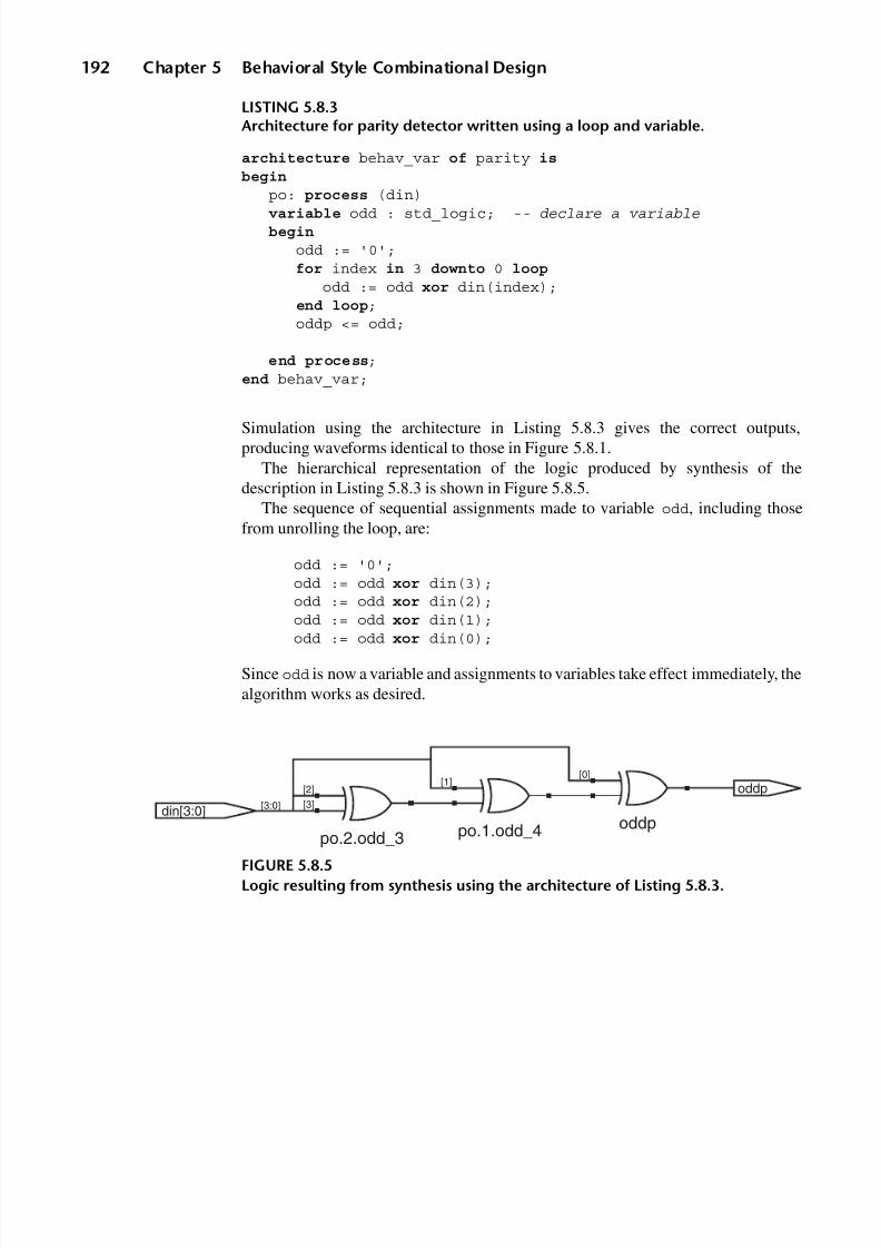
8/9/2019 VHDL for Engineers - Kenneth L. Short.pdf
http://slidepdf.com/reader/full/vhdl-for-engineers-kenneth-l-shortpdf 225/719

8/9/2019 VHDL for Engineers - Kenneth L. Short.pdf
http://slidepdf.com/reader/full/vhdl-for-engineers-kenneth-l-shortpdf 226/719
Section 5.9 Synthesis of Processes Describing Combinational Systems 193
5 .9 S YN TH ES IS OF P RO CE SS ES DE SC RI BI NG C O M B I N A T I O N AL S Y S T E M S
When a process is used to describe a combinational system, what is important is the
final result computed by the sequence of operations that comprises the algorithm, notthe sequence of operations itself. The synthesizer’s objective is to synthesize logicthat computes the same final result as the algorithm.
This fact is illustrated by the architecture description in Listing 5.8.3 for the oddparity detector. The hierarchical representation of the synthesized logic in Figure5.8.5 reflects the order of these assignments corresponding to the unrolled loop:
odd := '0';odd := odd xor din(3);odd := odd xor din(2);odd := odd xor din(1);
odd := odd xor din(0);
However, note that while the description is sequential, the synthesized logic iscombinational.
If the target PLD’s library has no XOR primitives larger than two-input XORgates, the hierarchical representation of the synthesized logic translates to thetechnology dependent flattened-to-gates representation in Figure 5.9.1. Here thefour-input XOR function is realized by a two-level combination of three two-inputXORs. The hierarchical representations of both the dataflow architecture in Listing5.8.1 (Figure 5.8.2) and the process architecture using a loop and variable in Listing5.8.3 (Figure 5.8.5) produce the same flattened-to-gates representation in Figure
5.9.1 when targeted to the same PLD.The 4-bit magnitude comparator in Listing 5.7.1 also illustrates the fact that what
is synthesized for a process is functionally equivalent to the overall effect of theprocess, rather than its sequential nature.
Synthesizing Loops As previously discussed, to synthesize a loop, a RTL synthesizer must unroll theloop. This requires that the number of loop iterations be known during synthesis.With respect to a for loop, this determination can be made if the loop’s rangebounds are statically deterministic. Thus, a for loop with constant bounds can besynthesized.
In contrast, if a variable were used in specifying the loop’s range bounds, thesynthesizer could not statically determine the number of loop iterations. Also, asynthesizer cannot statically determine the number of loop iterations of a while loop,

8/9/2019 VHDL for Engineers - Kenneth L. Short.pdf
http://slidepdf.com/reader/full/vhdl-for-engineers-kenneth-l-shortpdf 227/719
194 Chapter 5 Behavioral Style Combinational Design
since completion of a while loop is dependent on data generated during the loop’sexecution. Consequently, for loops with nonconstant bounds, all while loops, and
infinite loops cannot be synthesized.
Avoiding Latches To ensure that the logic synthesized from a process is combinational, all signals andvariables assigned a value in the process must be assigned a value each time theprocess executes. If this requirement is not met, latches may be inferred. To ensurethis requirement is met it might be helpful to assign a default value at the beginningof the process to each signal or variable that is assigned values later in the process.
PROBLE MS
5.1 Ifa changes from '1' to'0' in Listing 5.1.1, what is the order of process execution and why?
5.2 If carry_in changes from '0' to '1' in Listing 5.1.2, what is the order of processexecution and why?
5.3 What is the effect on the design of changing the textual order of the processes in thearchitecture body in Listing 5.1.2 so that process ha2 is first, followed byor1 and then ha1?Explain your answer.
FIGURE 5.9.1
Flattened-to-gates representation of four-input odd parity detector.
oddp
[3:0] [0] [0]din[3:0]
din_0_.O
[1]
[0]
[3]
[2]
oddpxor_3.O oddpxor.O oddp.O
[1] [1]
din_1_.O oddpxor_4.O
[2] [2]
din_2_.O
[3] [3]
din_3_.O

8/9/2019 VHDL for Engineers - Kenneth L. Short.pdf
http://slidepdf.com/reader/full/vhdl-for-engineers-kenneth-l-shortpdf 228/719
Problems 195
5.4 What causes a process with a sensitivity list to suspend its execution? What causes a processwithout a sensitivity list to suspend its execution?
5.5 What is a control statement? List VHDL’s control statements.
5.6 Write a behavioral style description of the logic circuit that follows. The description must havea separate process corresponding to each gate in the logic diagram. Each process must consist
of a single sequential signal assignment statement.
5.7 For the logic diagram shown below:
(a) Write an entity declaration for the circuit.(b) Write a behavioral style architecture that is functionally equivalent to the logic diagram.
This architecture must have a separate process for each gate. Label each process using thesame label as used in the logic diagram. The statement part of each process must containonly signal assignment statements.
(c) Write another behavioral style architecture that is functionally equivalent to the logicdiagram. This architecture must consist of only a single process.
5.8 Write a description of a combinational system that converts a BCD input code for a decimal
digit to the excess three (XS3) code for the same decimal digit. The input code is thestd_logic_vector bcd. The output code is the std_logic_vector xs3. Use a case statement todescribe the logic. Write the case statement so that the synthesizer can synthesize the leastamount of logic necessary to implement the converter.
5.9 The following truth table describes a function that must be implemented. In addition to thistruth table the specification for the system states that input combinations 110 and 111 willnever occur in the application:
Using a case statement, write a description that implements the function.
a b c w y
0 0 0 1 0
0 0 1 0 10 1 0 1 1
0 1 1 1 0
1 0 0 1 1
1 0 1 0 0
ab
c
fu0
u1
s1
a
b
c
fu2
u1
u0
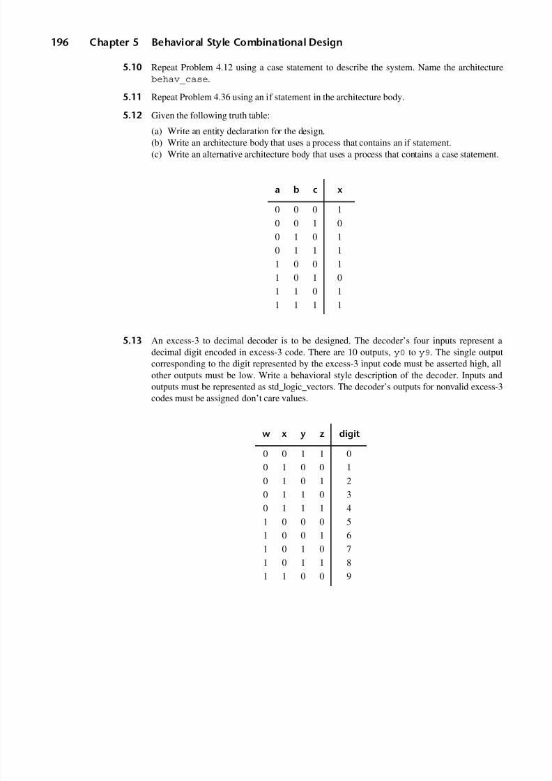
8/9/2019 VHDL for Engineers - Kenneth L. Short.pdf
http://slidepdf.com/reader/full/vhdl-for-engineers-kenneth-l-shortpdf 229/719
196 Chapter 5 Behavioral Style Combinational Design
5.10 Repeat Problem 4.12 using a case statement to describe the system. Name the architecturebehav_case.
5.11 Repeat Problem 4.36 using an if statement in the architecture body.
5.12 Given the following truth table:
(a) Write an entity declaration for the design.(b) Write an architecture body that uses a process that contains an if statement.(c) Write an alternative architecture body that uses a process that contains a case statement.
5.13 An excess-3 to decimal decoder is to be designed. The decoder’s four inputs represent adecimal digit encoded in excess-3 code. There are 10 outputs, y0 to y9. The single outputcorresponding to the digit represented by the excess-3 input code must be asserted high, allother outputs must be low. Write a behavioral style description of the decoder. Inputs andoutputs must be represented as std_logic_vectors. The decoder’s outputs for nonvalid excess-3
codes must be assigned don’t care values.
a b c x
0 0 0 1
0 0 1 0
0 1 0 1
0 1 1 1
1 0 0 11 0 1 0
1 1 0 1
1 1 1 1
w x y z digit
0 0 1 1 0
0 1 0 0 1
0 1 0 1 2
0 1 1 0 3
0 1 1 1 4
1 0 0 0 5
1 0 0 1 6
1 0 1 0 7
1 0 1 1 8
1 1 0 0 9
8/9/2019 VHDL for Engineers - Kenneth L. Short.pdf
http://slidepdf.com/reader/full/vhdl-for-engineers-kenneth-l-shortpdf 230/719
Problems 197
5.14 A two-to-one multiplexer has two data inputs, a and b, and one select input s. The multiplexerhas a single output c. If s = '0', c is equal to a. If s = '1', c is equal to b.(a) Write an entity declaration, namedmux, for the multiplexer. Use only the data type std_logic.(b) Write an architecture for mux, named if_bod, that uses a process statement containing
an if statement to describe the architecture.(c) Write an architecture for mux, named case_bod, that uses a process statement
containing a case statement to describe the architecture.
5.15 Given the following function:
(a) Write an entity declaration.(b) Write an architecture body named fcn_ife that uses an if statement to implement the
function.(c) Write an alternative architecture body name fcn_case that uses a case statement to
implement the function.
5.16 For the function specified by the truth table in Problem 4.24:
(a) Write a complete design description of the function in the truth table using a casestatement. Call the entity function_g. Treat the inputs as scalars in the entitydeclaration. Write the description so that the synthesizer can take advantage of the don’tcare cases to simplify the function.
(b) Write an alternative architecture for entity function_g that uses an if statement.
5.17 A Fairchild 74LCX257 IC is a quad two-input multiplexer with three-state outputs. When itsenable input oe_bar is asserted, it selects 4 bits of data from one of two sources i0 or i1,selected by a common select input s, to appear on its 4-bit output. When s is 0 it selects i0,when it is 1 it selects i1. When oe_bar is not asserted, the outputs are in their highimpedance state. Write an entity declaration named lcx257 for an equivalent system.Represent the data inputs as std_logic_vectorsi0 and i1. Name the output vector o. Write anarchitecture body named
behavioral for design entity
lcx257 that uses a process
containing nested if statements to describe the system.
5.18 Repeat the design of the thermometer to binary encoder in Problem 4.26, except write anarchitecture that uses a case statement that includes the assignment don’t care output values forinvalid input codes. Write an alternative architecture that uses an if statement and assigns don’tcare output values for invalid input codes.
5.19 A design entity named nand_8 is an eight-input NAND that has the following entitydeclaration:
entity nand_8 is port(
input : in std_logic_vector(7 downto 0); nand_out : out std_logic );end nand_8;
Write a behavioral style architecture body that uses a loop to describe nand_8.
f abc abc abc+ +=

8/9/2019 VHDL for Engineers - Kenneth L. Short.pdf
http://slidepdf.com/reader/full/vhdl-for-engineers-kenneth-l-shortpdf 231/719
198 Chapter 5 Behavioral Style Combinational Design
5.20 Write a behavioral style description of a 4-to-2 priority encoder. The input is thestd_logic_vectorx (3 down to 0) and the output is the std_logic_vector a (1 down to 0). Inputsare asserted low. The output is the binary equivalent of the index of the highest priority inputthat is asserted. Input x(3) has the highest priority. Use a for loop.
5.21 Write a description that has a behavioral style architecture for the 3-to-8 decoder described in
Listing 4.8.1. The behavioral style architecture should be based on either a select, if, or loopstatement. Before writing the actual code consider which construct is likely to provide the mostefficient coding.
5.22 Type unsigned, defined in package NUMERIC_STD, is similar to type std_logic_vector inthat its elements are type std_logic. It differs in that, in addition to the logical operatorsdefined for std_logic_vector, it has arithmetic operators, including an addition operator. Thisaddition operator can be used to add two unsigned vectors or to add an unsigned vector andan integer.
Consider a design entity having the following input and output:
inputs : in std_logic_vector(3 downto 0)
count : out std_logic_vector(1 downto 0)
Write an entity declaration named ones_count that has the input and output shown above.Write an architecture body named looped for entity ones_count. This architecture uses a
loop inside a process labeled p1 to determine the number of 1s in the input vector and outputs
the binary representation of this number as the value count. The architecture must describe
a combinational system.
5.23 Repeat the design of the thermometer to binary encoder in Problem 4.26, except write anarchitecture that primarily uses loop statements to implement the encoding. The approach can
be based on the observation that when the number of consecutive 1s in the input (starting from
therm(0)) is equal to the total number of 1s in the input, the input code is valid and the
output is equal to that number. The description must assign the outputs don’t care values for invalid input codes.
5.24 A combinational system takes as its inputs the votes from three judges and computes thewinner of a competition. Each judge has two switches, one for contestant A and one forcontestant B. Each judge must assign a 0 or a 1 to each contestant’s performance. The scoreassigned by each judge can be any of the four possible switch combinations to indicate any of four possible evaluations by that judge.
B A Outcome0 0 no decision0 1 A is the winner1 0 B is the winner1 1 tie
The switch outputs from each judge are combined to form two vectors, one for contestantA and one for contestant B. Each judge’s evaluation contributes one element to each vector.

8/9/2019 VHDL for Engineers - Kenneth L. Short.pdf
http://slidepdf.com/reader/full/vhdl-for-engineers-kenneth-l-shortpdf 232/719
Problems 199
Design entity tally takes the two vectors as inputs and computes the two-bit output namedwinner.
Winner Outcome0 0 no decision0 1 A is the winner—A has more 1 votes than B1 0 B is the winner—B has more 1 votes than A1 1 tie—A and B have an equal number of 1 votes
Given the following entity declaration for tally:
entity tally is port (scoresA, scoresB : in std_logic_vector (2 downto 0); winner : out std_logic_vector (1 downto 0));end entity;
Write an architecture named loopy that computes the output winner. The computation to
determine the winner must be performed using a loop statement. Use type integers in theintermediate computations for the final output value.
5.25 A system that is an eight-input AND is to be implemented by repeatedly iterating the twooperand VHDL AND operator.(a) Write a complete design description of this design entity using a behavioral style
architecture with a for loop.(b) If an eight-input NAND is required, can this be done by repeatedly iterating the two
operand VHDL NAND operator? Give an explanation of the basis for your answer.
5.26 Write a complete behavioral style description that uses a loop instruction to implement aneight-input NAND gate. The input to the gate is an 8-bit vector name inputs and the output
is named nandout. Name the entity nand8 and the architecture bhvloop.5.27 The 74AC280 is a 9-bit parity generator/checker IC that provides one output that indicates even
parity and a second output that indicates odd parity. Given the entity declaration:
entity ic74ac280 is port ( i: in std_logic_vector (8 downto 0); sum_even: out std_logic; sum_odd: out std_logic);end ic74ac280;
(a) Write a behavioral style architecture that uses looping to describe a circuit that isfunctionally equivalent to a 74AC280.
(b) Describe how using a loop statement would compare with using either a case or ifstatement for the architecture.

8/9/2019 VHDL for Engineers - Kenneth L. Short.pdf
http://slidepdf.com/reader/full/vhdl-for-engineers-kenneth-l-shortpdf 233/719
200 Chapter 5 Behavioral Style Combinational Design
5.28 Given the following truth table, write a complete VHDL design description of a designentity that accomplishes the function defined by the truth table below. Use a behavioral stylearchitecture that consists of two processes, one to assign a value to x and the other to assigna value to y.
a b c x y
0 0 0 0 1
0 0 1 1 0
0 1 0 0 1
0 1 1 0 0
1 0 0 1 0
1 0 1 0 0
1 1 0 0 0
1 1 1 0 1

8/9/2019 VHDL for Engineers - Kenneth L. Short.pdf
http://slidepdf.com/reader/full/vhdl-for-engineers-kenneth-l-shortpdf 234/719
201
Chapter 6
Event-Driven Simulation
Simulation is the process of conducting experiments on a model of a system for thepurpose of understanding or verifying the operation of the actual system.
Simulation is essential to the VHDL/PLD design methodology. Functionalsimulation verifies the functional operation of a description. Post-synthesis simulationverifies that the synthesizer accurately translated the description to logic. Timingsimulation verifies that the synthesized logic, when mapped to the target PLD, willmeet the system’s timing requirements.
Understanding how an event-driven simulator executes a VHDL program helpsclarify the semantics of many VHDL constructs. Construct semantics are defined in theIEEE Std 1076 Language Reference Manual (LRM) in terms of how an event-drivensimulator that is compliant with the standard must execute the constructs. Indeed, theprimary audiences for the LRM are simulation and synthesis tool developers.
Synthesis tool developers have as their primary objective creating a synthesizerthat synthesizes logic that behaves the same way as does the functional simulation of a design description.
This chapter provides a conceptual description of the internal operation of anevent-driven VHDL simulator. The simulator’s data structures and operations aredescribed. Simulations of some simple designs are discussed to illustrate each step inthe simulator’s operation.
6 . 1 S I MU LA TO R AP PR OAC H ES
VHDL is an event-driven language. A VHDL program represents the discrete eventsimulation of a physical system. Discrete event simulation allows deterministicmodeling of concurrency.

8/9/2019 VHDL for Engineers - Kenneth L. Short.pdf
http://slidepdf.com/reader/full/vhdl-for-engineers-kenneth-l-shortpdf 235/719
202 Chapter 6 Event-Driven Simulation
Requirements for aVHDL Simulator
A VHDL simulator must provide data structures and algorithms that allow it toefficiently simulate the execution of concurrent statements in a VHDL program.These concurrent statements must be simulated by a simulator program that is beingexecuted sequentially on a host computer. In other words, the simulator’s sequentialexecution must be able to provide the illusion of concurrency.
A simulator must also efficiently produce an accurate representation of the outputwaveforms that result from the application of a set of input values to the design entitybeing simulated. Since the number of signals in a design can be very large, simulatormemory efficiency and speed are important.
Simulation Time During a simulation, changes in input and output signals occur in simulation time,the time value maintained by the simulator, as opposed to real time. Each change inthe value of a signal is an event .
Kinds of Simulators Based on their approach to performing simulation, there are three common kinds of simulators for digital systems: time driven, event driven, and cycle based.
For these different simulation approaches the arrows in Figure 6.1.1 indicate atwhich simulation times the simulator must execute simulation cycles to computeoutput values.
Time-DrivenSimulation
In a time-driven simulation, simulation time is advanced in predetermined uniformincrements. As time is advanced, any events in the next time step are simulated. Thefixed size of the time step determines the resolution with which events can beobserved. For example, simulation time might be advanced in 1 ns steps. During atime-driven simulation, there are typically a very large number of time steps duringwhich there are no events. Nevertheless, a time-driven simulator must execute asimulation cycle for each time step.
Event-DrivenSimulation
In an event-driven simulation, time is advanced in nonuniform steps whose sizesdepend on when events occur (Figure 6.1.1). An event-driven simulator responds toeach input event by executing a sequence of simulation cycles that determine whenand to what values the simulated system’s signals change.
Advantages of
Event-DrivenSimulation
Event-driven simulation eliminates the need for the simulator to evaluate the model
at the empty time steps (those without events) that are evaluated in a time-drivensimulation. Since the state of a system only changes in response to input events,these events are sufficient to determine when the model must be evaluated.
In event-driven simulation, simulation time is advanced in a single step from thecurrent simulation time to the next scheduled event. Intervals of time in which thereare no events are skipped, without affecting the validity of the simulation results.This approach results in faster and more precise simulations.

8/9/2019 VHDL for Engineers - Kenneth L. Short.pdf
http://slidepdf.com/reader/full/vhdl-for-engineers-kenneth-l-shortpdf 236/719

8/9/2019 VHDL for Engineers - Kenneth L. Short.pdf
http://slidepdf.com/reader/full/vhdl-for-engineers-kenneth-l-shortpdf 237/719
204 Chapter 6 Event-Driven Simulation
SimulationProcesses
The process statement is the basic behavioral statement in VHDL. Every concurrentVHDL statement has an equivalent process representation. The term simulation process
is used in this book to mean a process that is equivalent to some concurrent statement ina design entity’s architecture and is used for the simulation of that statement.
Elaboration Elaboration is the creation of a simulation model for a design entity from its VHDLdescription. This simulation model resides in the host computer’s memory andconsists of a net (network) of simulation processes.
Simulation Net During elaboration, all concurrent statements are converted to equivalent simulationprocesses. Any VHDL program can ultimately be viewed as a collection of simulationprocesses communicating through signals, that is, a simulation net . The resultingsimulation net is executed to simulate the design entity’s behavior.
Flattening
a HierarchicalStructure
During elaboration, a design that has a hierarchical structure is flattened until the
entire design is described by a simulation net. In addition, all of the data objectsdeclared in the description are created.
Elaboration starts with the top-level design entity. Each concurrent statement inthe architecture of the top-level design entity is converted into correspondingsimulation processes.
Creating SimulationProcesses
The discussion that follows focuses on process, signal assignment, and componentinstantiation statements, but a transformation to a simulation process exists for allconcurrent statements.
Converting aProcess to aSimulation Process
A process statement is elaborated directly into a simulation process. The steps involvedare:
• The process declarative part is elaborated; all the declared data objects arecreated and their initial values are determined.
• The drivers required by the process statement are created.
• The initial transaction, defined by the initial value specified in a signal’sdeclaration or, if no initial value is specified, the default value, is placed in eachsignal’s driver.
The creation of signal drivers is discussed in detail in the next section.
Converting aConcurrent SignalAssignment to aSimulation Process
A concurrent signal assignment statement is first converted to an equivalent processstatement. A Boolean expression concurrent signal assignment statement has animplied sensitivity list that includes all the signals on the right-hand side of theassignment symbol. A selected signal assignment statement’s implied sensitivitylist includes all the signals in its select expression. A conditional signal assignmentstatement’s implied sensitivity list includes all the signals in its conditions. Ineffect, a concurrent signal assignment statement is nothing more than a shorthand
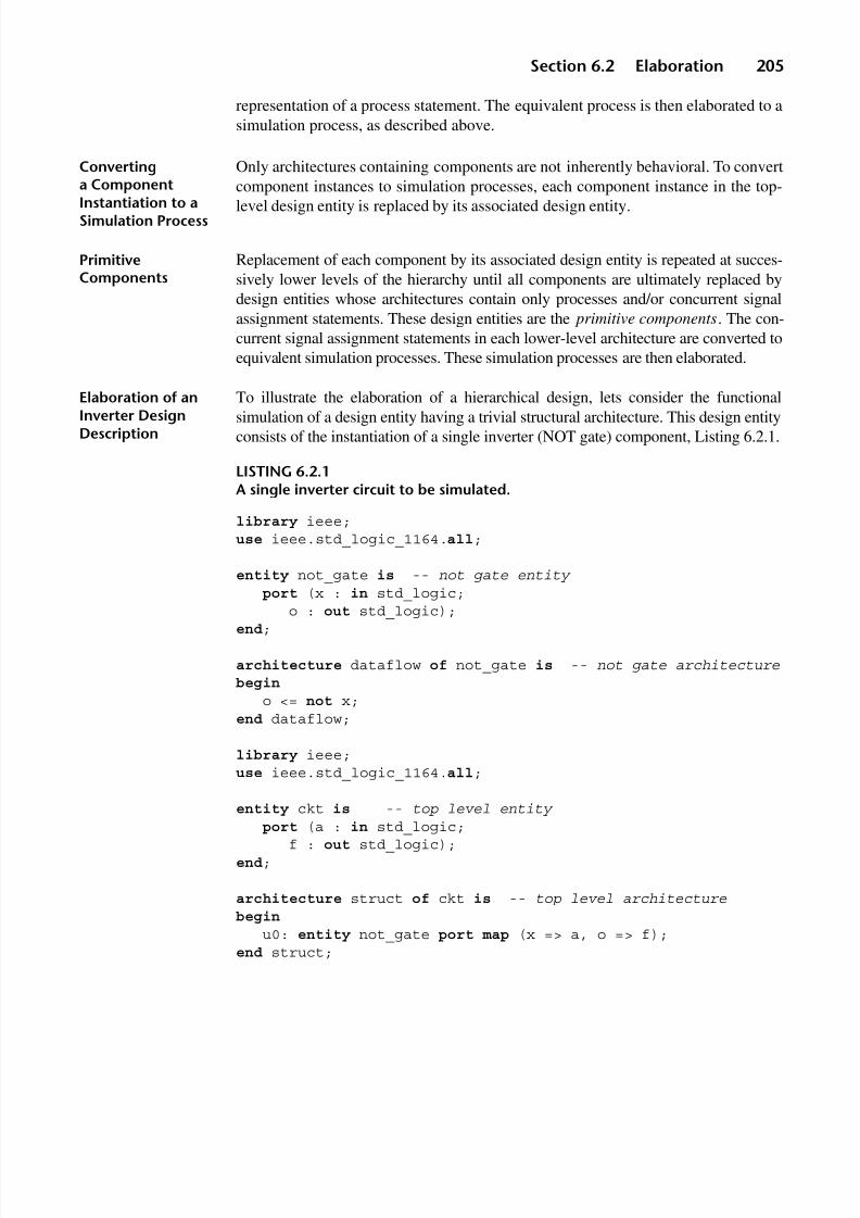
8/9/2019 VHDL for Engineers - Kenneth L. Short.pdf
http://slidepdf.com/reader/full/vhdl-for-engineers-kenneth-l-shortpdf 238/719
Section 6.2 Elaboration 205
representation of a process statement. The equivalent process is then elaborated to asimulation process, as described above.
Convertinga Component
Instantiation to aSimulation Process
Only architectures containing components are not inherently behavioral. To convertcomponent instances to simulation processes, each component instance in the top-
level design entity is replaced by its associated design entity.
PrimitiveComponents
Replacement of each component by its associated design entity is repeated at succes-sively lower levels of the hierarchy until all components are ultimately replaced bydesign entities whose architectures contain only processes and/or concurrent signalassignment statements. These design entities are the primitive components. The con-current signal assignment statements in each lower-level architecture are converted toequivalent simulation processes. These simulation processes are then elaborated.
Elaboration of an
Inverter DesignDescription
To illustrate the elaboration of a hierarchical design, lets consider the functional
simulation of a design entity having a trivial structural architecture. This design entityconsists of the instantiation of a single inverter (NOT gate) component, Listing 6.2.1.
LISTING 6.2.1A single inverter circuit to be simulated.
library ieee;use ieee.std_logic_1164.all;
entity not_gate is -- not gate entity port (x : in std_logic;
o : out std_logic);end;
architecture dataflow of not_gate is -- not gate architecturebegin
o <= not x;end dataflow;
library ieee;use ieee.std_logic_1164.all;
entity ckt is -- top level entity port (a : in std_logic; f : out std_logic);end;
architecture struct of ckt is -- top level architecturebegin
u0: entity not_gate port map (x => a, o => f);end struct;

8/9/2019 VHDL for Engineers - Kenneth L. Short.pdf
http://slidepdf.com/reader/full/vhdl-for-engineers-kenneth-l-shortpdf 239/719
206 Chapter 6 Event-Driven Simulation
This design file contains two design entities. The not_gate design entity app-ears first. The second design entity, ckt, is the circuit whose operation we wish toverify. Design entity ckt has an input a and an output f. The architecture for ckt isstructural and consists of a single instantiation of a not_gate.
To simulate ckt we use a testbench named testbench. Design entity ckt is theUUT in design entity testbench. Since the testbench is now the top level of thehierarchy, what we will actually simulate is testbench (Figure 6.2.1). In thisexample, the same names, a and f, used for the UUT’s ports are also used for thesignals in the testbench that connect to these ports.
Listing 6.2.2, for testbench, has a mixed style architecture consisting of asingle component instantiation and a single process.
The component instantiation, labeled uut, is an instance of the design entity ckt,whose operation we wish to verify. Since a component instantiation statement is not
behavioral, the elaboration must go down a hierarchical level and elaborate the archi-tecture for ckt.
LISTING 6.2.2Testbench for inverter circuit of Listing 6.2.1.
library ieee;use ieee.std_logic_1164.all;
entity testbench is
end testbench;
architecture behavior of testbench is
signal a : std_logic; signal f : std_logic;
begin
uut: entity ckt port map (a => a,f => f);
FIGURE 6.2.1
Relationship of the testbench to the circuit being tested.
testbench tb
a a ffnot_gate
ckt
uut/u0

8/9/2019 VHDL for Engineers - Kenneth L. Short.pdf
http://slidepdf.com/reader/full/vhdl-for-engineers-kenneth-l-shortpdf 240/719

8/9/2019 VHDL for Engineers - Kenneth L. Short.pdf
http://slidepdf.com/reader/full/vhdl-for-engineers-kenneth-l-shortpdf 241/719
208 Chapter 6 Event-Driven Simulation
Simulation Net forInverter Testbench
The simulation net created by this elaboration is represented in Figure 6.2.2. Eachcircle represents a simulation process. The directed arrow from tb to uut/u0
indicates that tb assigns a value to a and that uut/u0 is sensitive to a. Thedashed directed arrow from uut/u0 to tb indicates that uut/u0 assigns a valueto f and that tb reads this value. A dashed directed arrow is used to distinguishthat although tb reads f, it is not sensitive to f (does not have f in its sensitivitylist).
6 . 3 S I GN AL DR I V E R S
During elaboration, for each signal assigned a value in a simulation process a signaldriver is created. This signal driver is associated with the simulation processcontaining the signal assignment statement. Only one signal driver is created for
each signal assigned a value in a simulation process. This is true even if a simulationprocess contains multiple assignments to the same signal.
Multiply DrivenSignals
If only one simulation process in a simulation model contains assignments to aparticular signal, elaboration will produce only one driver for that signal. If two (ormore) different simulation processes contain assignments to the same signal, elabo-ration will produce two (or more) different drivers for that signal, one associatedwith each simulation process. Such a signal is multiply driven.
Signal Driversas Data Queues
In terms of a simulator’s data structures, a signal driver is modeled as a queue. Eachsignal driver queue is defined by all of the signal assignment statements that assignvalues to a particular signal in a simulation process.
Transactions Each time a signal assignment statement is executed, the simulator posts (schedules)a transaction in the signal’s driver. Each transaction is a pair consisting of a valuecomponent and a time component.
FIGURE 6.2.2
Simulation net from the elaboration of top-level design entity testbench inListing 6.2.2.
tb uut/u0
a
f

8/9/2019 VHDL for Engineers - Kenneth L. Short.pdf
http://slidepdf.com/reader/full/vhdl-for-engineers-kenneth-l-shortpdf 242/719
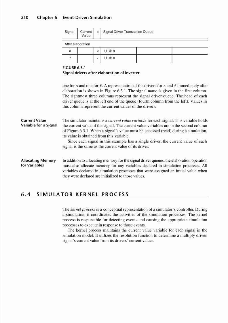
8/9/2019 VHDL for Engineers - Kenneth L. Short.pdf
http://slidepdf.com/reader/full/vhdl-for-engineers-kenneth-l-shortpdf 243/719
210 Chapter 6 Event-Driven Simulation
one for a and one for f. A representation of the drivers for a and f immediately afterelaboration is shown in Figure 6.3.1. The signal name is given in the first column.The rightmost three columns represent the signal driver queue. The head of eachdriver queue is at the left end of the queue (fourth column from the left). Values inthis column represent the current values of the drivers.
Current ValueVariable for a Signal
The simulator maintains a current value variable for each signal. This variable holdsthe current value of the signal. The current value variables are in the second columnof Figure 6.3.1. When a signal’s value must be accessed (read) during a simulation,its value is obtained from this variable.
Since each signal in this example has a single driver, the current value of eachsignal is the same as the current value of its driver.
Allocating Memoryfor Variables
In addition to allocating memory for the signal driver queues, the elaboration operationmust also allocate memory for any variables declared in simulation processes. Allvariables declared in simulation processes that were assigned an initial value whenthey were declared are initialized to those values.
6 . 4 S I MU LA TOR K ER NE L PR OC ESS
The kernel process is a conceptual representation of a simulator’s controller. Duringa simulation, it coordinates the activities of the simulation processes. The kernel
process is responsible for detecting events and causing the appropriate simulationprocesses to execute in response to those events.
The kernel process maintains the current value variable for each signal in thesimulation model. It utilizes the resolution function to determine a multiply drivensignal’s current value from its drivers’ current values.
FIGURE 6.3.1
Signal drivers after elaboration of inverter.
Signal CurrentValue
<
After elaboration
a < ‘U’ @ 0
f < ‘U’ @ 0
Signal Driver Transaction Queue

8/9/2019 VHDL for Engineers - Kenneth L. Short.pdf
http://slidepdf.com/reader/full/vhdl-for-engineers-kenneth-l-shortpdf 244/719

8/9/2019 VHDL for Engineers - Kenneth L. Short.pdf
http://slidepdf.com/reader/full/vhdl-for-engineers-kenneth-l-shortpdf 245/719
212 Chapter 6 Event-Driven Simulation
Active ProcessesQueue
The simulator maintains an active processes queue. All simulation processes thatneed to be run during a particular simulation cycle are placed in the active processesqueue by the kernel. The kernel then takes each simulation process from this queueand executes it until it suspends.
Waiting ProcessesQueue
If a simulation process is suspended because of the execution of a wait statement of the form wait for time_expression, that simulation process is put in the waiting
processes queue in time order. The simulation process is, therefore, scheduled foractivation after a period of time equal to time_expression from the currentsimulation time. A simulation process in the waiting processes queue is referred to asa scheduled process because it is scheduled to be resumed (be placed in the activeprocesses queue) at a specific future time.
NonsuspendingProcess
It is syntactically legal to have a process statement without a sensitivity list or waitstatement(s). After elaboration, this results in a simulation process without a sensi-
tivity list or wait statement(s). However, when simulated, such a process neversuspends, simulation time does not advance, and the simulation hangs if a simulationcycle limit is not set.
6 .5 S IM UL AT IO N I NI TI AL IZ AT ION
After elaboration is completed, simulation consists of an initialization phase followedby repetitive execution of simulation cycles. The time values referred to in thefollowing discussions are simulation times, as maintained by the simulator’s clock.
Initialization Phase At the beginning of the initialization phase, the current time (Tc) is set to 0(Figure 6.5.1).
Initial Executionof All SimulationProcesses
The kernel places all of the simulation processes in the active processes queue. Eachsimulation process is then taken from this queue and executed until it suspends. Theorder of execution of simulation processes during initialization is not important. Theinitial execution of each simulation process ensures that all initial transactions arescheduled, so that the simulation may continue.
A simulation process is suspended either implicitly or explicitly. A process with asensitivity list is suspended implicitly after its sequential statements have beenexecuted to the end of the process. A process with one or more wait statements issuspended explicitly when its first wait statement is executed.

8/9/2019 VHDL for Engineers - Kenneth L. Short.pdf
http://slidepdf.com/reader/full/vhdl-for-engineers-kenneth-l-shortpdf 246/719
Section 6.5 Simulation Initialization 213
Specifying Delays inSignal Assignments In writing synthesizable descriptions, we use signal assignments with zero delay, forexample:
x <= a and b;
FIGURE 6.5.1
Initialization phase of an event-driven simulation.
Initialization
Active processes
queue empty?
Initializationcomplete
Tc 0
Put all processeson active
processes queue
Take a processfrom the active
processes queueand execute it
until it suspends
Schedule any newsignal transactions
in signal drivers
No
Yes

8/9/2019 VHDL for Engineers - Kenneth L. Short.pdf
http://slidepdf.com/reader/full/vhdl-for-engineers-kenneth-l-shortpdf 247/719
214 Chapter 6 Event-Driven Simulation
In contrast, timing models of actual hardware and some testbenches use signalassignment statements that include an after clause. The after clause specifies theexact delay from the current time for the assignment to take effect. For example:
x <= a and b after 2 ns;
This statement might describe an AND gate in a PLD. The output changes 2 ns aftera change in a or b. This delay is the result of the propagation delay of signals throughthe physical circuit.
It is not appropriate to use an assignment that specifies a delay in a description to besynthesized. At the time we write a description, we may not have chosen a target PLD.In addition, since the propagation delay in the physical implementation depends onmany factors, including device technology, architecture, routing, and the operationalenviornment, a synthesizer cannot guarantee that a specified delay can be achieved.Accordingly, a synthesizer simply ignores after clauses in signal assignment state-ments. The syntax of assignment statements with after clauses is discussed in Chapter 7
in the context of their use in testbenches.
Delta Delays Execution of a simulation process may cause transactions to be added to the driverqueues for some signals. If a signal assignment without an after clause is executed,the associated transaction is assigned a time component 1 delta (δ) delay greater thanthe current simulation time.
A delta delay is an infinitesimal period of time. It is used as a scheduling deviceto ensure a clear order of events in circuits with zero delay devices (devices with nodelay specified). This is necessary so that a circuit’s operation can be simulated in acorrect and repeatable fashion.
Two-DimensionalView of SimulationTime
Since a delta delay is infinitesimal, when added to the current simulation time it doesnot advance the numerical time value. Conceptually, simulation time is viewed astwo dimensional. If delta delays are added, simulation time increases on the Y axis,leaving its numerical time step value on the X axis unchanged.
FIGURE 6.5.2
Deltas at each simulation time step for the inverter simulation.
0
1
2
0 ns 20 ns 40 ns time step
delta step
60 ns

8/9/2019 VHDL for Engineers - Kenneth L. Short.pdf
http://slidepdf.com/reader/full/vhdl-for-engineers-kenneth-l-shortpdf 248/719
Section 6.6 Simulation Cycles 215
This concept is illustrated in Figure 6.5.2, which represents one delta occuring at
simulation time 0 and two deltas occurring at simulation time steps at 20 and 40 ns.The deltas are shown stacked on top of each other at each time step, producing a“two-dimensional” time representation. The stacking of deltas indicates that theiroccurrence does not advance the numerical value of simulation time. Delta delaysare discussed further in Section 6.8.
Inverter ExampleSignal Drivers afterInitialization
Returning again to our inverter example, the second entry (second group of tworows) in Figure 6.5.3 shows the drivers for the inverter example after initialization.
When simulation process tb is executed at initialization, the first statement is await statement that causes tb to suspend for 20 ns, without placing any transactions
in any signal drivers. Accordingly, tb is placed in the waiting processes queue.When simulation process uut/u0 is executed at initialization, the statement:
f <= not a;
is executed and then the process suspends. This puts the transaction 'U' @ 0 +
1 δ in the driver for f. This transaction has the value component 'U' because thenot operator for std_logic operating on 'U' returns 'U'. Since the assignmentstatement does not have an after clause, the time component is 1 δ.
6 . 6 S I M UL A T I ON C Y C L E S
After the initialization phase, all simulation processes are in their suspended states.The first simulation cycle is then executed.
SimulationCycle Phases
A simulation cycle consists of two phases: an update phase and an execution phase.These phases are described in detail in the following paragraphs.
FIGURE 6.5.3
Signal drivers from elaboration through initialization of inverter.
Signal Value <
After elaboration
a < ‘U’ @ 0
f < ‘U’ @ 0
a < ‘U’ @ 0
f < ‘U’ @ 0
‘U’
‘U’
‘U’
‘U’
Signal Driver Transaction Queue
After initialization Tc 0, Tn 0 1
‘U’ @ 0 1

8/9/2019 VHDL for Engineers - Kenneth L. Short.pdf
http://slidepdf.com/reader/full/vhdl-for-engineers-kenneth-l-shortpdf 249/719
216 Chapter 6 Event-Driven Simulation
Update PhaseOverview
The update phase first determines the next value for the current simulation time andadvances the simulator clock to this value. Based on this new simulation time, adetermination is made as to whether the simulation is complete.
If the simulation is not complete, all signals scheduled to be updated at the currentsimulation time are updated.
A change in a signal’s value can occur only during the update phase of asimulation cycle. If a signal’s update results in an event, all simulation processessensitive to this event are placed in the active processes queue. This determination iscarried out for all signals that are updated. In addition, all simulation processes thatare scheduled to resume at the current simulation time are placed in the activeprocesses queue. The active processes queue now contains all of the simulationprocesses that need to be executed during the current simulation cycle.
Update PhaseDetails
Steps in the update phase are shown in detail in Figure 6.6.1. At the beginning of theupdate phase, the simulator clock is advanced to the next simulation time.
Next SimulationTime
The next simulation time (Tn) is determined as either:
1. One delta greater than the current simulation time (Tc + δ), if there is a trans-action in any signal driver with a time component of Tc + δ. Since a delta is aninfinitesimal increment in time, this does not advance the numerical value of the current simulation time.
2. The next time step. The next time step is the earliest of either:
• TIME’HIGH,
• The time component of the transaction whose time component is the smallestvalue greater than Tc + δ, or
• The earliest time at which a process is scheduled to resume.
SimulationComplete?
The next simulation time is then checked against TIME’HIGH, which is the limitplaced on how long the simulation is to run. If Tn equals TIME’HIGH, and there areno signal drivers with transactions scheduled for Tn or simulation processes scheduledto resume at Tn, the simulation is complete.
If the simulation is not complete, the current simulation time is set equal to thenext simulation time (Tc = Tn). If Tn is equal to Tc + δ, the next simulation cycle iscalled a delta simulation cycle.
Update Signals Each signal whose driver has a transaction with a time component equal to thecurrent simulation time (is scheduled for the current simulation time) has its valueupdated to the value component of the transaction.
Determinationof Processes toResume
If none of these updates cause a signal’s value to change, then there are no events. If there are no events and no processes are scheduled to resume, the simulation iscomplete.

8/9/2019 VHDL for Engineers - Kenneth L. Short.pdf
http://slidepdf.com/reader/full/vhdl-for-engineers-kenneth-l-shortpdf 250/719
Section 6.6 Simulation Cycles 217
FIGURE 6.6.1
Simulation cycle update phase for an event-driven simulator.
Simulation cycle
Update signals
having
transactions at Tc
Tn TIME'HIGH and
no active drivers or scheduled
process resumptions?
End of simulation
Events on
updated signals?
Active processes
queue empty?
Yes
No
Yes
No
Are there any
transactions at
Tcdelta?
Tn Tc deltaYesNo
Tn next timestep
1
Put sensitive
processes on active
processes queue
Yes
2
No
Tc Tn
No
Processes
scheculed to
resume at Tc?
Put scheduled
processes on active
processes queue
Yes

8/9/2019 VHDL for Engineers - Kenneth L. Short.pdf
http://slidepdf.com/reader/full/vhdl-for-engineers-kenneth-l-shortpdf 251/719
218 Chapter 6 Event-Driven Simulation
If there are one or more events, each simulation process that is sensitive to thoseevents (has a signal in its sensitivity list on which an event occurred) is placed in theactive processes queue for execution.
If there are processes scheduled to resume at the current simulation time, they arealso placed in the active processes queue. These processes become active indepen-
dently of any events.
Execution Phase During the execution phase, Figure 6.6.2, each simulation process in the activeprocesses queue is taken from that queue and executed until it suspends. Executionof a simulation process may cause the execution of one or more signal assignmentstatements. Execution of a signal assignment statement causes one or more transac-tions to be scheduled for the specified signal’s driver. After all simulation processesthat were in the active processes queue have been executed, the simulator starts thenext simulation cycle.
The order in which the kernel takes simulation processes from the active
processes queue and executes them is not important, because these processes are con-current.
FIGURE 6.6.2
Simulation cycle execution phase.
Active processqueue empty?
Take next processfrom active
processes queueand execute it until
it suspends
Post new signaltransactions tosignal drivers
Yes
No
1
2

8/9/2019 VHDL for Engineers - Kenneth L. Short.pdf
http://slidepdf.com/reader/full/vhdl-for-engineers-kenneth-l-shortpdf 252/719
Section 6.6 Simulation Cycles 219
When Do SignalsTake New Values?
It is not until a simulation process suspends that the transactions resulting from
signal assignments in that process are placed in the appropriate signal driver
queues. Thus, in a single simulation process, if two or more signal assignment state-ments that assign values to the same signal are each executed, it is the lastassignment executed before the simulation process suspends that determines the
value component of the transaction placed in the driver. It is not until the update phase of the next simulation cycle, after all the
simulation processes that were in the active processes queue during the current
simulation cycle have been executed and suspended, that any signals assigned
values by these processes are updated. That is, values assigned by simulationprocesses in the execution phase of one simulation cycle don’t take effect until theupdate phase of the next simulation cycle, at the earliest.
In our design descriptions, the time at which a value should be assigned to asignal is not specified in the signal assignment statement. Therefore, the timedefaults to one delta delay from the current time. This means that the assignment of
a new value to a signal cannot take effect until the update phase of the next
simulation cycle. This is after the process containing the assignment has
suspended. Therefore, the simulation process does not see the effect of any signal
assignment until the next time it resumes.
For a signal assignment with an after clause, the effect of the assignment does nottake affect until simulation time has advanced by the amount equal to the timeexpression in the after clause.
From this discussion, we see that a signal’s value is only indirectly modified by anassignment statement, with the effect occurring no sooner than 1 δ later.
Summary of
Simulation CycleSteps
A simulation cycle consists of the following steps:
1. The time of the next simulation cycle is determined. If Tn = Tc + δ, the nextsimulation cycle is a delta simulation cycle.
2. Simulation is complete if Tn = TIME’HIGH and there are no signal driverswith transactions scheduled for Tn (active drivers) or simulation processesscheduled to resume at Tn.
3. If the simulation is not complete, the current simulation time Tc is set to Tn.
4. The values of all signals having transactions scheduled for Tc are updated.Events may occur on some signals as a result of updating their values.
5. All processes that are sensitive to the events in (4) are put in the active processes
queue.6. All processes scheduled to resume at Tc are also put in the active processes queue.
7. Each simulation process is taken from the active processes queue and executeduntil it suspends. Execution of simulation processes may cause new transactionsto be posted in signal drivers.
8. Return to step 1.

8/9/2019 VHDL for Engineers - Kenneth L. Short.pdf
http://slidepdf.com/reader/full/vhdl-for-engineers-kenneth-l-shortpdf 253/719

8/9/2019 VHDL for Engineers - Kenneth L. Short.pdf
http://slidepdf.com/reader/full/vhdl-for-engineers-kenneth-l-shortpdf 254/719

8/9/2019 VHDL for Engineers - Kenneth L. Short.pdf
http://slidepdf.com/reader/full/vhdl-for-engineers-kenneth-l-shortpdf 255/719
222 Chapter 6 Event-Driven Simulation
For conciseness, a simulation cycles list only shows deltas where an event
occurred. Therefore, the transaction at 0 + 1 δ is not shown because that transactionassigned a value of 'U' to f, but f previously had the value 'U'.
Each time step after t = 0 results from the testbench simulation process tbbecoming active at the end of a wait period (at 20, 40, and 60 ns). When tb executesat the 20 and 40 ns time steps, it schedules a transaction to the driver for a at thecurrent simulation time + 1 δ. Since the value of a can’t change until the updatephase of the next simulation cycle, there are no events during these 0 δ cycles and,therefore, there are no 0 δ entries in the simulation cycles listing in Figure 6.6.1 atthe 20 and 40 ns time steps.
Activation of tb at 60 ns does not appear in the list because that execution causedno signal assignments to be made, therefore no events could result.
Figure 6.6.5 represents the number of deltas (delta simulation cycles) that occur
at each time step.
Table 6.6.1Simulation cycles listing for inverter.
ns δδδδ a f
0 0 U U
20 1 1 U
20 2 1 0
40 1 0 0
40 2 0 1
FIGURE 6.6.5
Delta cycles for each simulation time step for inverter simulation.
0
1
2
0 ns 20 ns 40 ns time step
delta step
60 ns
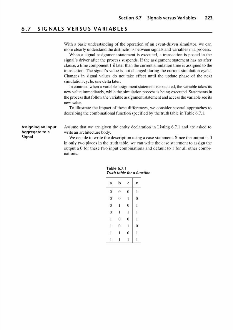
8/9/2019 VHDL for Engineers - Kenneth L. Short.pdf
http://slidepdf.com/reader/full/vhdl-for-engineers-kenneth-l-shortpdf 256/719
Section 6.7 Signals versus Variables 223
6 .7 S IG NA LS V ER SU S VA RI AB LE S
With a basic understanding of the operation of an event-driven simulator, we canmore clearly understand the distinctions between signals and variables in a process.
When a signal assignment statement is executed, a transaction is posted in thesignal’s driver after the process suspends. If the assignment statement has no afterclause, a time component 1 δ later than the current simulation time is assigned to thetransaction. The signal’s value is not changed during the current simulation cycle.Changes in signal values do not take effect until the update phase of the nextsimulation cycle, one delta later.
In contrast, when a variable assignment statement is executed, the variable takes itsnew value immediately, while the simulation process is being executed. Statements inthe process that follow the variable assignment statement and access the variable see itsnew value.
To illustrate the impact of these differences, we consider several approaches to
describing the combinational function specified by the truth table in Table 6.7.1.
Assigning an InputAggregate to aSignal
Assume that we are given the entity declaration in Listing 6.7.1 and are asked towrite an architecture body.
We decide to write the description using a case statement. Since the output is 0in only two places in the truth table, we can write the case statement to assign theoutput a 0 for these two input combinations and default to 1 for all other combi-nations.
Table 6.7.1Truth table for a function.
a b c x
0 0 0 1
0 0 1 0
0 1 0 1
0 1 1 1
1 0 0 1
1 0 1 0
1 1 0 1
1 1 1 1

8/9/2019 VHDL for Engineers - Kenneth L. Short.pdf
http://slidepdf.com/reader/full/vhdl-for-engineers-kenneth-l-shortpdf 257/719
224 Chapter 6 Event-Driven Simulation
LISTING 6.7.1Case description of truth table with an invalid sensitivity list.
library ieee;use ieee.std_logic_1164.all;
entity truth_table is port ( a, b, c : in std_logic; x : out std_logic);end truth_table;
architecture casey of truth_table is
signal abc : std_logic_vector( 2 downto 0); begin
tt: process (a, b, c) -- invalid sensitivity list begin
abc <= (a, b, c); case abc is
when "001" | "101" => x <= '0'; when others => x <= '1'; end case; end process;
end casey;
The case statement is simpler to write if the inputs are treated as a vector inside theprocess. The architecture body in Listing 6.7.1 uses this approach. To accomplish this,
signal abc is declared as a std_logic_vector in the architecture’s declarative part andthe first statement in the process assigns aggregate (a, b, c) to the std_logic_vectorabc. Signal abc is then used as the expression in the case statement.
This description compiles without error. Simulation produces the waveforms inFigure 6.7.1. The testbench starts with all inputs as 0s, then counts through the inputcombinations in binary. Each input combination is applied for 50 ns.
FIGURE 6.7.1
Timing waveform for description in Listing 6.7.1.

8/9/2019 VHDL for Engineers - Kenneth L. Short.pdf
http://slidepdf.com/reader/full/vhdl-for-engineers-kenneth-l-shortpdf 258/719
Section 6.7 Signals versus Variables 225
Examination of the simulation waveforms shows the output is 0 when the inputsare 010 (2) and 110 (6), rather than when they are 001 (1) and 101 (5), as desired. Itappears that the correct output is delayed by one input count. In a sense, it is.
Further examination of the simulation cycles list reveals the source of theproblem (Table 6.7.2). Assume that the inputs are 000 and that the testbench
assigns input c a '1' at 50 ns (+ 0 δ). During the update phase of the nextsimulation cycle, one delta cycle later at 50 ns + 1 δ, the input is changed to 001.This event on c causes the process tt to be executed, since c is in the process’ssensitivity list.
The first statement in the process assigns the new value 001 to signal abc. However,when this assignment statement is executed it only schedules a transaction in the driverfor abc for a value of "001" at 50 ns + 2 δ. However, simulation time is still at 50 ns +1 δ, so the value of abc is unchanged.
Next, the case statement is executed while abc is still "000", so the others clauseexecutes. The assignment statement in the others clause schedules a transaction tomake x a '1' at 50 ns + 2 δ. The simulation cycle ends and simulation time changesto 50 ns + 2 δ.
Table 6.7.2Simulation cycles list for description of Listing 6.7.1.
ns delta a b c UUT/abc x
0 0 U U U UUU U
0 1 0 0 0 UUU 1
0 2 0 0 0 000 1
50 1 0 0 1 000 150 2 0 0 1 001 1
100 1 0 1 0 001 1
100 2 0 1 0 010 0
150 1 0 1 1 010 0
150 2 0 1 1 011 1
200 1 1 0 0 011 1
200 2 1 0 0 100 1
250 1 1 0 1 100 1
250 2 1 0 1 101 1
300 1 1 1 0 101 1
300 2 1 1 0 110 0
350 1 1 1 1 110 0
350 2 1 1 1 111 1
400 1 0 0 0 111 1
400 2 0 0 0 000 1

8/9/2019 VHDL for Engineers - Kenneth L. Short.pdf
http://slidepdf.com/reader/full/vhdl-for-engineers-kenneth-l-shortpdf 259/719
226 Chapter 6 Event-Driven Simulation
During the simulation cycle at 50 ns + 2 δ, the value of abc is updated andchanges from "000" to "001". Thus, there is an event on abc. The signal x is alsoupdated, but it remains '1' so there is no event on x. Since the only event is on abc,and abc is not in the tt simulation process’s sensitivity list, the process is notexecuted during this (50 ns + 2 δ) simulation cycle. We are left with output x equal
to '1' for an input of "001", which is incorrect.If we had included signal abc in our sensitivity list, simulation process tt would
be executed during the execution phase of the simulation cycle at 50 + 2 δ. Thismissing execution of simulation process tt would have occurred with abc equal"001" and the case statement would schedule a transaction to assign the value '0'
to x at 50 ns + 3 δ. The next simulation cycle would be at 50 ns + 3 δ. During theupdate phase of this simulation cycle, x would be changed to '0' and we wouldhave the correct output.
The next simulation cycle is at 100 ns (+ 0 δ) when the testbench assigns input ba '1' and input c a '0'. One delta cycle later at 100 ns + 1 δ, the inputs are changedto "010". Since both b and c change values, there are events on b and c. Either of these events is sufficient to cause simulation process tt to be executed during theexecution phase of this simulation cycle. Execution of the assignment to abc
schedules a transaction for abc to become "010" at 100 ns + 2 δ. The case statementis then executed. With abc still having the value of "001", the first assignmentstatement in the case statement is executed. This assignment statement schedules atransaction to make x a '0' at 100 ns + 2 δ. The simulation cycle then terminates.
Since there are transactions in the drivers of abc and x with time components of 100 ns + 2 δ, the next simulation cycle is at 100 ns + 2 δ. During the update phase of this simulation cycle, abc is changed to "010" and x is changed to '0'. Now outputx has the value it should have had for the previous input combination. Since neither
abc nor x is in simulation process tt's sensitivity list, this process is not executed.
Signals Requiredin a Sensitivity List
This example emphasizes the fact that a process must include all relevant signals inits sensitivity list. For a combinational design, the sensitivity list must include all thesignals read by the process. A process may read more signals than just those that areinputs to the design entity. In this example, the case statement reads abc, since abcis the case expression.
Including an InputAggregate in
Sensitivity List
We have already mentioned one approach to solving the problem. Simply, includesignal abc in the sensitivity list. This may at first seem odd, since the signal abc is not
an input to the circuit. However, the previous analysis shows that this is necessary forcorrect operation.
Placing theAssignment of theAggregate Outsideof the Process
Another approach would be to place the signal assignment statement that assigns theaggregate to abc outside of the process and make the process sensitive to only abc.This architecture body is shown in Listing 6.7.2.

8/9/2019 VHDL for Engineers - Kenneth L. Short.pdf
http://slidepdf.com/reader/full/vhdl-for-engineers-kenneth-l-shortpdf 260/719

8/9/2019 VHDL for Engineers - Kenneth L. Short.pdf
http://slidepdf.com/reader/full/vhdl-for-engineers-kenneth-l-shortpdf 261/719

8/9/2019 VHDL for Engineers - Kenneth L. Short.pdf
http://slidepdf.com/reader/full/vhdl-for-engineers-kenneth-l-shortpdf 262/719
Section 6.7 Signals versus Variables 229
architecture casey of truth_table is
begin
process (a, b, c)
variable abc : std_logic_vector(2 downto 0);
begin
abc := (a, b, c); case abc is
when "001" | "101" => x <= '0'; when others => x <= '1'; end case; end process;
end casey;
Variable abc must be declared inside the process and is local to the process.When the variable assignment statement is executed, the variable’s value is changedimmediately. Next, when the case statement is executed, it uses the new value of abcthat was assigned during the current simulation cycle.
Signal and VariableDistinctions
Some distinctions between signals and variables in an architecture are now summarized.Signals in an architecture:
• Must be declared outside of any processes.
• Are visible to all processes (and other concurrent statements) in thearchitecture in which they are declared and are used to carry informationbetween concurrent statements in the architecture.
• Have current and projected (future) values.
• Retain their values between executions of a process.
• A signal assignment schedules a transaction in the signal’s driver queue. If thesignal assignment has no after clause, the assigned value takes effect at theupdate phase of the next simulation cycle (one δ later). If there is an after clausein the assignment, the assigned value does not take effect until the update phaseof the simulation cycle at the specified time.
• An initial value specified in a signal’s declaration is not synthesizable.
Variables in an architecture:
• Can only be declared within processes or subprograms.
• Are not visible outside of the process or subprogram in which they aredeclared.

8/9/2019 VHDL for Engineers - Kenneth L. Short.pdf
http://slidepdf.com/reader/full/vhdl-for-engineers-kenneth-l-shortpdf 263/719
230 Chapter 6 Event-Driven Simulation
• Retain their values between executions of the process in which they aredeclared.
• Do not retain their values between executions of the subprogram in which theyare declared.
• An initial value specified in a variable’s declaration in a process is not
synthesizable.
Another advantage of using variables rather than signals is that signals require largecomplicated data structures in the simulator to maintain their data queues. As a result,in complex designs using variables instead of signals results in reduced memoryrequirements and faster simulations.
6 . 8 DE L TA D E LA Y S
We have seen how delta delays are used in event-driven simulation. At first, it mayseem that they simply complicate matters. However, in this section we see why theiruse is necessary.
Delta Delay as aSchedulingMechanism
A delta delay is a scheduling mechanism used to ensure a deterministic order of events in circuits having devices with no specified delays. This is necessary so that acircuit’s operation can be simulated in a repeatable fashion.
Another, seemingly contradictory, way of stating this is that delta delays arenecessary to allow order independence to be achieved in the simulation of concurrentstatements. It has been stated that the order of execution of concurrent statements
during a simulation does not affect simulation results. The use of delta delays allowsa simulator to ensure that this is true when concurrent statements have signal assign-ments with no specified delays.
Simulation ProcessExecution OrderIndependence
It has also been stated that during a simulation cycle the order in which the simulationprocesses are executed does not affect simulation results. This follows from the require-ment that the order in which concurrent statements in an architecture are executed doesnot affect simulation results.
Consider the two-level logic circuit in Figure 6.8.1(a), which is stimulated andmonitored by a testbench. The corresponding simulation net is given in Figure 6.8.1(b).
If we were manually performing a functional evaluation of output f in terms of values applied to inputs a, b, and c, we would most likely first apply a new set of values to a, b, and c. Next we would compute the new value of s1. Then we wouldcompute the new value of f. This would most likely be our order of evaluation,because we naturally think of information flowing from the inputs of the gates totheir outputs. If we think of the simulation processes associated with the testbenchand the gates in the simulation net, we would naturally think that we must executethese processes in this same order to determine the result.
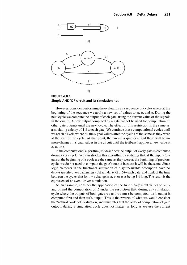
8/9/2019 VHDL for Engineers - Kenneth L. Short.pdf
http://slidepdf.com/reader/full/vhdl-for-engineers-kenneth-l-shortpdf 264/719

8/9/2019 VHDL for Engineers - Kenneth L. Short.pdf
http://slidepdf.com/reader/full/vhdl-for-engineers-kenneth-l-shortpdf 265/719
232 Chapter 6 Event-Driven Simulation
signal values for all computations during that cycle and continue the simulationcycles until there are no further changes in signal values (events).
In Figure 6.8.2, a copy of the circuit is given for each cycle resulting from theapplication of the first binary input values to a, b, and c. In Figure 6.8.2, new signalvalues are shown in parentheses to the right of current signal values only if the new
value is different from the current value. The new values don’t take effect (are notused) until the next cycle. The testbench and gates are shaded if they must executeduring the current cycle.
As can be seen from Figure 6.8.2, the order of execution (computation of gateoutputs) does not matter as long as each cycle computes using the current signalvalues and the cycles are continued until there are no more signal changes. For
FIGURE 6.8.2
Cycles in the computation of AND/OR circuit output for application of oneinput combination.
(a)
a
b
c
f
UU (0)
U (0)
U (0)
u0u1
s1
tb
(b)
a
b
c
f
U0
0
0
u0u1
s1
tb
(c)
a
b
c
f
U (0)0
0
0
u0u1
s1
tb
(d)
a
b
cf
00
0
0
u0u1
s1
tb
0
0
U (0)
U

8/9/2019 VHDL for Engineers - Kenneth L. Short.pdf
http://slidepdf.com/reader/full/vhdl-for-engineers-kenneth-l-shortpdf 266/719

8/9/2019 VHDL for Engineers - Kenneth L. Short.pdf
http://slidepdf.com/reader/full/vhdl-for-engineers-kenneth-l-shortpdf 267/719
234 Chapter 6 Event-Driven Simulation
LISTING 6.8.1Structural description of two-level gate circuit from Figure 6.8.3.
library ieee;use ieee.std_logic_1164.all;
entity delta_2gates is port (a : in std_logic; f : out std_logic);end delta_2gates;
architecture struct of delta_2gates is
signal s1 : std_logic;begin
u0: entity not_gate port map (a, s1); u1: entity nand_2 port map (s1, a, f);
end struct;
LISTING 6.8.2Behavioral description of two-level gate circuit.
library ieee;use ieee.std_logic_1164.all;
entity delta_2gates is
port ( a : in std_logic; f : out std_logic);end delta_2gates;
architecture behavioral of delta_2gates is
signal s1 : std_logic;begin
u1: process ( a, s1 ) begin
f <= a nand s1; end process u1;
u0: process ( a )
begin
s1 <= not a; end process u0;
end behavioral;

8/9/2019 VHDL for Engineers - Kenneth L. Short.pdf
http://slidepdf.com/reader/full/vhdl-for-engineers-kenneth-l-shortpdf 268/719
Section 6.9 Delta Delays and Combinational Feedback 235
The simulation net resulting from elaboration, including the testbench simulationprocess, is shown in Figure 6.8.4. This net is the same for either description,
With a previously '0', the testbench assigns a value of '1' to a at 20 ns. Thisassignment takes effect at 20 ns + 1 δ. The simulation cycles listing, Table 6.8.1,
shows the glitch occurring at simulation time 20 ns + 2 δ.This simulator waveform shows the glitch as a tick mark above the waveform for
f at 20 ns (Figure 6.8.5).
6 .9 D EL TA D EL AY S A ND C OM BI NA TI ON AL FE E DBAC K
As another example of the use of delta delays, consider the NAND gate circuit withcombinational feedback in Figure 6.9.1. As previously discussed (“Avoiding Combi-
national Loops” on page 155), feedback is to be avoided in combinational designdescriptions. Here we consider how the simulator handles combinational feedback when it is encountered.
FIGURE 6.8.4
Simulation process net for two-level gate circuit.
tb uut/u1
uut/u0a s1
a
f
Table 6.8.1Simulation cycles listing for three gate circuit.
ns δδδδ a f
0 0 U U
0 1 0 U
0 2 0 1
20 1 1 1
20 2 1 0
20 3 1 1

8/9/2019 VHDL for Engineers - Kenneth L. Short.pdf
http://slidepdf.com/reader/full/vhdl-for-engineers-kenneth-l-shortpdf 269/719
236 Chapter 6 Event-Driven Simulation
Assume input enable is '0' for 50 ns and then is changed to a '1' for 350 ns.Functional simulation produces the waveforms in Figure 6.9.2 and an error message:“Delta count overflow - stopped. Try to increase the iterations limit in simulator
preferences.” The simulation stopped after 50 ns, instead of continuing for 400 ns.Closer examination reveals that when the simulation starts, enable is a '0' and
the output of the NAND gate is a '1'. This '1' is fed back to the NAND gate’s topinput, but does not cause the gate’s output to change. The circuit is stable.
However, at 50 ns, enable is changed to a '1' by the testbench. This inputchange takes effect at 50 ns + 1 δ. This causes the NAND gate’s output (and its topinput) to change to '0' at 50 ns +2 δ. This in turn causes the NAND gate’s output(and its top input) to change to '1' at 50 ns +3 δ. In effect, when its bottom input isa '1', the NAND simply inverts the value at its top input. The new output value iscontinually fed back and inverted. As a result, the NAND’s output and its top inputchange state every delta. Thus, the circuit is unstable and oscillates.
The simulation process for this circuit has enable and s1 in its sensitivity list.Since there is an event on s1 during every delta cycle, the simulation process executesevery delta cycle, scheduling a change in the value of s1 for 1 δ later. This causes still
another delta cycle.
Simulator DeltaCycle Limit
The simulator has a limit set on the maximum number of delta cycles in a time step.In this example, that limit is surpassed and simulation is never advanced past the 50ns time step. Increasing the delta cycle limit will not solve the problem because thenumber of cycles required is infinite.
A timing simulation of the circuit targeted to a PLD with a 10 ns delay is given inFigure 6.9.3.
FIGURE 6.8.5
Waveform showing output glitch.
FIGURE 6.9.1
NAND circuit with combinational feedback.
enable sigout
s1
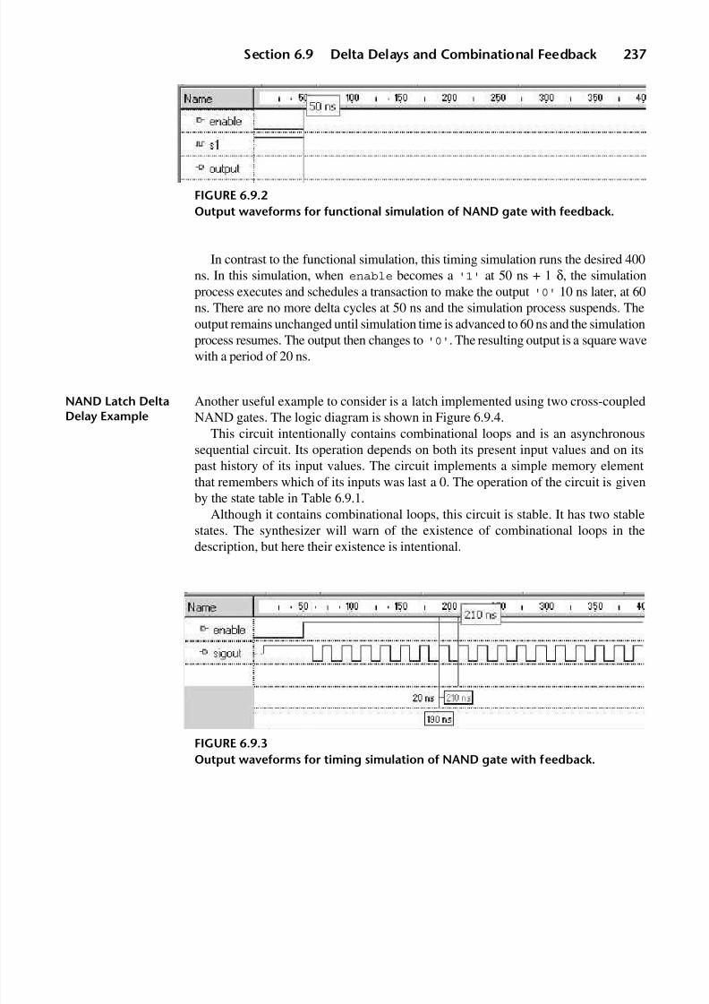
8/9/2019 VHDL for Engineers - Kenneth L. Short.pdf
http://slidepdf.com/reader/full/vhdl-for-engineers-kenneth-l-shortpdf 270/719
Section 6.9 Delta Delays and Combinational Feedback 237
In contrast to the functional simulation, this timing simulation runs the desired 400ns. In this simulation, when enable becomes a '1' at 50 ns + 1 δ, the simulationprocess executes and schedules a transaction to make the output '0' 10 ns later, at 60ns. There are no more delta cycles at 50 ns and the simulation process suspends. Theoutput remains unchanged until simulation time is advanced to 60 ns and the simulation
process resumes. The output then changes to '0'. The resulting output is a square wavewith a period of 20 ns.
NAND Latch DeltaDelay Example
Another useful example to consider is a latch implemented using two cross-coupledNAND gates. The logic diagram is shown in Figure 6.9.4.
This circuit intentionally contains combinational loops and is an asynchronoussequential circuit. Its operation depends on both its present input values and on itspast history of its input values. The circuit implements a simple memory elementthat remembers which of its inputs was last a 0. The operation of the circuit is givenby the state table in Table 6.9.1.
Although it contains combinational loops, this circuit is stable. It has two stablestates. The synthesizer will warn of the existence of combinational loops in thedescription, but here their existence is intentional.
FIGURE 6.9.2
Output waveforms for functional simulation of NAND gate with feedback.
FIGURE 6.9.3
Output waveforms for timing simulation of NAND gate with feedback.

8/9/2019 VHDL for Engineers - Kenneth L. Short.pdf
http://slidepdf.com/reader/full/vhdl-for-engineers-kenneth-l-shortpdf 271/719
238 Chapter 6 Event-Driven Simulation
A behavioral description of the circuit is given in Listing 6.9.1.An interesting aspect of this description is that its functional simulation depends
on nonzero gate propagation delays to function properly. The simulator’s use of delta
delays meets this requirement.
LISTING 6.9.1Behavioral description of NAND latch.
library ieee;use ieee.std_logic_1164.all;
entity nand_latch is
port (s_bar, r_bar : in std_logic; q, q_bar: inout std_logic);end nand_latch;
architecture behavioral of nand_latch is
FIGURE 6.9.4
Set–reset latch from two cross-coupled NAND gates.
s_bar
r_bar
q
q_bar
s1
s2
u0
u1
Table 6.9.1State table for set–reset latch.
s_bar r_bar q q_bar
0 0 ? ?
0 1 1 0
1 0 0 1
1 1 q q_bar

8/9/2019 VHDL for Engineers - Kenneth L. Short.pdf
http://slidepdf.com/reader/full/vhdl-for-engineers-kenneth-l-shortpdf 272/719

8/9/2019 VHDL for Engineers - Kenneth L. Short.pdf
http://slidepdf.com/reader/full/vhdl-for-engineers-kenneth-l-shortpdf 273/719
240 Chapter 6 Event-Driven Simulation
LISTING 6.10.1 (Cont.)
en_b_bar: in std_logic; d_bus: out std_logic );end three_state_bus;
architecture three_state_bus of three_state_bus is
begin
u1: process (d_a, en_a_bar) begin
if en_a_bar = '0' then
d_bus <= d_a; else
d_bus <= 'Z'; end if;
end process u1;
u2: process (d_b, en_b_bar) begin
if en_b_bar = '0' then
d_bus <= d_b; else
d_bus <= 'Z'; end if; end process u2;
end three_state_bus;
Process u1 has two assignment statements that assign values to d_bus. Sincethese assignment statements are in the same process, only one driver for d_bus iscreated by this process. Accordingly, elaboration creates a single driver for d_bus
from u1 (u1/d_bus).
FIGURE 6.10.1
Waveform from simulation of two three-state buffers with a common output.

8/9/2019 VHDL for Engineers - Kenneth L. Short.pdf
http://slidepdf.com/reader/full/vhdl-for-engineers-kenneth-l-shortpdf 274/719
Section 6.11 Signal Attributes 241
Process u2 also has two signal assignment statements for d_bus. Since theseassignment statements are in a different process, a second driver for d_bus is created(u2/d_bus). The actual value of d_bus is the resolved value from the current valuesof drivers u1/d_bus and u2/d_bus.
The output waveform for a simulation of this circuit is shown in Figure 6.10.1.The input to three-state buffer u1 is fixed at '0' and the input for three-state bufferu2 is fixed at '1'. Both buffers are initially disabled. At 50 ns buffer u1 is enabled.At 100 ns it is disabled. At 150 ns buffer u2 is enabled.
The listing of delta cycles from the simulation is given in Table 6.10.1.Signal drivers for the buffer outputs are represented in Figure 6.10.2. There are
two separate drivers for d_bus, u1/d_bus and u2/d_bus. However, there is onlyone current value variable for d_bus. In Figure 6.10.2 the current value variable isshown to the left of the signal name.
After initialization, the testbench schedules transactions for the inputs at the0 δ cycle of each time step. To reduce the amount of space required for the figure, the0 δ cycles for each time step are not shown. Since transactions are only scheduled onthe input drivers at those times, no events are possible during these delta cycles.
The value of the current value variable in column one is obtained by the std_logicresolution function operating on the current driver values for that simulation cycle.
6 . 11 S I GN A L AT T RI B UT E S
VHDL’s attribute feature allows us to extract information about an object (such as asignal, variable, or type) that may not be directly related to the object’s value. Thisinformation can be used in a description or a testbench. Attributes also allow us toassign additional information to objects that can be useful for synthesis.
Table 6.10.1Simulation cycles listing for simulation of two three-state buffers withcommon output.
ns d d_a en_a_bar d_b en_b_bar d_bus
0 0 U U U U U
0 1 0 1 1 1 Z
50 1 0 0 1 1 Z
50 2 0 0 1 1 0
100 1 0 1 1 1 0
100 2 0 1 1 1 Z
150 1 0 1 1 0 Z
150 2 0 1 1 0 1

8/9/2019 VHDL for Engineers - Kenneth L. Short.pdf
http://slidepdf.com/reader/full/vhdl-for-engineers-kenneth-l-shortpdf 275/719
242 Chapter 6 Event-Driven Simulation
Predefined andUser-DefinedAttributes
There are two classes of attributes: predefined and user defined. Predefined attributes
are defined in IEEE Std 1076. User-defined attributes are defined outside of thestandard, by tool vendors or by us. For example, we have seen attributes defined by aplace and route tool vendor to assign signals to pin numbers in Listing 1.10.1.
FIGURE 6.10.2Signal drivers during simulation of three-state bus circuit.
Signal Driver Transaction Queue
After elaboration
SignalValue
d_bus u1/d_bus <
u2/d_bus
After initialization Tc 0, Tn 0 1
u1/d_bus <
<u2/d_bus
<
<
‘U’ @ 0 ‘Z’ @ 0 1
‘U’ @ 0 ‘Z’ @ 0 1
‘0’ @ 50 2
‘Z’ @ 100 + 2
‘1’ @ 150 2
‘U’
After simulation cycle Tc 0 1 , Tn 50
u1/d_bus <
<u2/d_bus
‘Z’ @ 0 1
‘Z’ @ 0 1
‘Z’
After simulation cycle Tc 50 1 , Tn 50 2
u1/d_bus <
<u2/d_bus
‘Z’ @ 0 1
‘Z’ @ 0 1
‘Z’
After simulation cycle Tc 50 + 2 , Tn 100
u1/d_bus <
<u2/d_bus
‘0’ @ 50 2
‘Z’ @ 0 1
‘0’
After simulation cycle Tc 100 1, Tn 100 2
u1/d_bus <
<u2/d_bus
‘0’ @ 50 2
‘Z’ @ 0 1
‘0’
After simulation cycle Tc 100 + 2 , Tn 150
u1/d_bus <
<u2/d_bus
‘Z’ @ 100 2
‘Z’ @ 0 1
‘Z’
After simulation cycle Tc 150 1, Tn 150 2
u1/d_bus <
<u2/d_bus
‘Z’ @ 100 2
‘Z’ @ 0 1
‘Z’
After simulation cycle Tc 150 + 1 , Tn done
u1/d_bus <
<u2/d_bus
‘Z’ @ 100 2
‘1’ @ 150 2
‘1’

8/9/2019 VHDL for Engineers - Kenneth L. Short.pdf
http://slidepdf.com/reader/full/vhdl-for-engineers-kenneth-l-shortpdf 276/719
Section 6.11 Signal Attributes 243
One way of categorizing attributes is by the kind of results they return. Whencategorized this way there are five kinds of predefined attributes. Value attributes
return a constant value. Function attributes call a function that returns a value.Signal attributes create a new implicit signal. Type attributes return a type. Range
attributes return a range.
Predefined SignalAttributes
Predefined attributes are always applied to a prefix (such as a signal or variable name,or a type or subtype name). Predefined attributes can also be categorized by the kindof prefix involved. Given a signal S and a value t, VHDL defines the signal attributes
listed in Table 6.11.1. Signal attributes provide information about the history of trans-actions and events on signals. A clear understanding of signal attributes is predicatedon an understanding of simulation cycles in event-driven simulation. Accordingly,these attributes are introduced in this chapter and are used in later chapters.
Implicit Signals The first four attributes create new signals from other signals. The signals created are
called implicit signals; they have no explicit declarations.The first attribute in Table 6.11.1, the transaction attribute, creates an implicit
type bit signal that changes value (toggles) each time there is a transaction on itsprefix signal.
Table 6.11.1Predefined signal attributes.
Attribute Result
S’Transaction Implicit bit signal whose value is changed in each simulation cycle inwhich a transaction occurs on S (signal S becomes active).
S’Stable(t) Implicit boolean signal. True when no event has occurred on S for t timeunits up to the current time, False otherwise.
S’Quiet(t) Implicit boolean signal. True when no transaction has occurred on S fort time units up to the current time, False otherwise.
S’Delayed(t) Implicit signal equivalent to S, but delayed t units of time.
S’Event A boolean value. True if an event has occurred on S in the currentsimulation cycle, False otherwise.
S’Active A boolean value. True if a transaction occurred on S in the currentsimulation cycle, False otherwise.
S’Last_event Amount of elapsed time since last event on S, if no event has yetoccurred it returns TIME’HIGH.
S’Last_active Amount of time elapsed since last transaction on S, if no transaction hasyet occurred it returns TIME’HIGH.
S’Last_value Previous value of S immediately before last event on S.
(Cont.)

8/9/2019 VHDL for Engineers - Kenneth L. Short.pdf
http://slidepdf.com/reader/full/vhdl-for-engineers-kenneth-l-shortpdf 277/719
244 Chapter 6 Event-Driven Simulation
For example, assume that signal sig has been explicitly declared as a std_logicsignal. Execution of the concurrent signal assignment statement
sig <= '0', '0' after 5 ns, '1' after 10 ns, '0' after 20 ns, '1' after 25 ns, '1' after 35 ns;
during the initialization phase of a simulation posts six transactions to the driver forsig. The transactions are for simulation times 0, 5, 10, 20, 25, and 35 ns.
The waveforms for signal sig and sig'transaction are given in Figure 6.11.1.For each transaction posted to sig, implicit signal sig'transaction toggles.
Of the six transactions, only four cause events on sig. These events are at 0, 10, 20,and 25 ns. The event at simulation time 0 changes sig’s value from 'U' to '0'.
The next three attributes in Table 6.11.1 take an optional time parameter. At-tributes stable and quiet create implicit signals of type boolean. Attribute stable istrue if there has been no event on its prefix signal for the specified time prior to thecurrent time. In Figure 6.11.1 the time specified for the stable attribute is 5 ns. As a
result, attribute sig'stable(5ns) is false until simulation time 5 ns, at whichpoint it becomes true. However, since there is an event on sig at 10 ns, sig'stable(5ns) becomes false at that time.
Table 6.11.1 (Cont.)
Attribute Result
S’Driving True if the process is driving S or every element of a composite S, orFalse if the current value of the driver for S or any element of S in
the process is determined by the null transaction.
S’Driving_value Current value of the driver for S in the process containing theassignment statement to S.
FIGURE 6.11.1
Some signal attributes for the signal sig.
Name Type
sig std_logic
sig'TRANSACTION bit
sig'STABLE(5ns) boolean
sig'QUIET(5ns) boolean
sig'DELAYED(8ns) std_logic
sig'DELAYED(8ns)'TRANSACTION bit
sig‘EVENT
sig‘ACTIVE
false true false true false
false true false true
true
false
boolean
boolean

8/9/2019 VHDL for Engineers - Kenneth L. Short.pdf
http://slidepdf.com/reader/full/vhdl-for-engineers-kenneth-l-shortpdf 278/719
Problems 245
Attribute quiet is true if there has been no transaction on its prefix signal for thespecified time prior to the current time. In Figure 6.11.1 the time specified for the quietattribute is 5 ns. As a result, attribute sig'quiet(5ns) is false until simulation time15 ns, at which point it becomes true. However, since there is a transaction on sig at20 ns, sig'quiet(5ns) becomes false at that time.
The delayed attribute creates an implicit signal that is the same type as its prefix,but is delayed by the time specified. In Figure 6.11.1, the signal corresponding toattribute sig'delayed(8ns) is shown. This is simply the signal sig shifted right8 ns. For the first 8 ns this signal has the value 'U'.
For the attribute delayed, if the time parameter is omitted, then t = 0 + 1 δ is thedefault. That is, the delayed signal is delayed 1 δ. For the other two attributes, if thisparameter is omitted, a default value of 0 fs is assumed.
Since an implicit signal is a signal, it also has attributes. Figure 6.11.1 shows thesignal created by the attributed transaction applied to the implicit signalsig'delayed(8ns). This creates the implicit signal sig'delayed(8ns)'trans-action.
The event and active attributes return boolean values, not signals. The eventattribute is true only during a simulation cycle where its prefix signal has an event.The active attribute is true only during a simulation cycle where there is a transactionon its prefix signal. Though they are not signals, the values of sig'event andsig'active are shown as waveforms on Figure 6.11.1.
Note that the implicit signals created are viewable on a waveform editor when anyof the first four attributes in Table 6.11.1 are used in a description or testbench.
Attributes last_event and last_active return values of type time that correspondto the time elapsed since the last event or last transaction, respectively, on theirprefix signals. This is not the time of the last event or transaction, but rather the
amount of time that has passed since the last event or transaction. For example, if the current simulation time is 37 ns, sig'last_event is 12 ns and sig'last_
active is 2 ns.Attribute last_value gives the value its prefix signal before its last event. If there
has been no event on its prefix signal, attribute last_value returns the current value of the prefix signal. For example, if the current simulation time is 37 ns, sig'last_value is '0'.
Signal attributes are often used in checking timing behavior within a model, asdiscussed in Chapters 7 and 14.
PROBLE MS
6.1 List the three common kinds of simulators for digital systems. What are the relative speeds of these simulators? Which one of these simulators cannot be used to simulate a combinationalsystem and why?
6.2 What kind of simulator is specified in the VHDL LRM?

8/9/2019 VHDL for Engineers - Kenneth L. Short.pdf
http://slidepdf.com/reader/full/vhdl-for-engineers-kenneth-l-shortpdf 279/719
246 Chapter 6 Event-Driven Simulation
6.3 If the input to a system being functionally simulated changes twice in a 2 ms interval of simulation time and we wished to be able to simulate events with a resolution of 1 ns, howmany times would a time-based simulator have to evaluate the model in the 2 ms time interval?For the same conditions, how many times would an event-driven simulator have to evaluate themodel?
6.4 List the three steps an event driven-simulator performs to accomplish a simulation.6.5 Given the following function:
(a) Write an entity declaration and three alternative architectures for a system that computes thefunction. Each architecture must consist of a single concurrent signal assignment statement.The first architecture must use a Boolean expression. The second must use a selected signalassignment statement. The third must use a conditional signal assignment statement.
(b) For each of the concurrent signal assignment statements in part (a), write a correspondingsimulation process.
6.6 Assume that the circuit described in Problem 5.7 is the UUT in a testbench. The testbenchstimulus process named tb applies all possible input combinations to the UUT. Draw and labelthe simulation net that results from elaboration of the testbench.
6.7 Assume that a testbench applies every possible input combination to the half-adder designentity described in Listing 2.6.1. The testbench has a component instantiation with the labeluut that instantiates the half adder and a process with the label tb that applies the stimulus.
(a) Write the code for the simulation processes that would result from elaboration of thetestbench, except for process tb.
(b) Draw a completely labeled diagram of the simulation net (includingtb) resulting from theelaboration.
(c) Draw the signal driver queues that would be produced by the elaboration.(d) Assuming that when testbench process
tb is first executed it assigns the value
'0' to both
a and b, list the values for all of the inputs and outputs for each simulation cycle frominitialization through the end of the time step at 0 ns.
6.8 Assume that the design entity from Problem 2.29 is described by a structural style architecture.Also assume that a testbench has been written that uses a process named tb to apply inputs tothe design entity and monitor its output.
(a) Write the code for all of the simulation processes created by elaboration, except for theprocess tb.
(b) Draw a diagram of the simulation net including tb.(c) Assuming that when the testbench is simulated it first applies input combination “000” at
time 0 + 0 δ, write a list of all the signal values for all δs at time step 0.
6.9 A testbench is used to simulate the program in Problem 2.30. Design entity gate_ckt isinstantiated as component uut in the testbench. Component nand_2 is a two-input NANDfunction and component invert is an inverter (NOT) function. The first statement in stimulusprocesstb in the testbench applies inputs a, b,c = "000". Every 50 ns tb applies a new binarytest vector whose value is 1 greater than the previous test vector, until all input combinations havebeen applied.
(a) Draw a simulation net showing the simulation processes produced when the simulatorelaborates the testbench.
y a b c+⋅=

8/9/2019 VHDL for Engineers - Kenneth L. Short.pdf
http://slidepdf.com/reader/full/vhdl-for-engineers-kenneth-l-shortpdf 280/719
Problems 247
(b) Write VHDL processes corresponding to the simulation processes that are producedduring elaboration of u0, u1, and u2.
(c) Provide a listing of all the simulation deltas along with the signal values starting frominitialization up to and including 50 ns.
6.10 Given the following architecture body:
architecture mixed of fcn is signal s1, s2 : std_logic ;begin
u0: s1 <= '1' when a = '0' and b = '1' else '0';
u1: with std_logic_vector'(a, c) select s2 <= '1' when "11", '0' when others;
u2: process (s1, s2)
begin f <= s1 or s2; end process;
end mixed;
(a) Write the entity declaration for the design entity.(b) Write each of the simulation processes created by elaboration.(c) Assuming a testbench contains a process tb, which applies all possible input values and
verifies the output, draw a diagram of the simulation net. Assume that the instantiation ofthe design entity in the testbench is labeled uut.
6.11 Under what conditions will a signal have multiple signal drivers?
6.12 List the possible states a simulation process can be in and what happens to the process in each state.
6.13 What happens during the initialization phase of a simulation and why?
6.14 Given the following architecture for a testbench for a half adder:
architecture waveform of testbench is
signal a_tb, b_tb : std_logic; signal sum_tb, carry_out_tb : std_logic;
begin
UUT : entity half_adder port map (a => a_tb, b => b_tb, sum => sum_tb, carry_out => carry_out_tb );
stim_a: a_tb <= '0', '1' after 40 ns; stim_b: b_tb <= '0', '1' after 20 ns, '0' after 40 ns, '1' after 60 ns;
end waveform;
8/9/2019 VHDL for Engineers - Kenneth L. Short.pdf
http://slidepdf.com/reader/full/vhdl-for-engineers-kenneth-l-shortpdf 281/719
248 Chapter 6 Event-Driven Simulation
(a) Draw the driver queues for a_tb and b_tb immediately after the initialization phase ofthe simulation.
(b) If the architecture for the half adder contains the following two statements:
u0: sum <= a xor b;u1: carry_out <= a and b;
draw a diagram of the simulation net created after elaboration.(c) Write the simulation process corresponding to the instruction labeled stim_b in the
testbench.(d) Provide the complete simulation cycle listing for time step 0 (include all the associated
delta cycles).
6.15 Given the following design entity description:
library ieee;use ieee.std_logic_1164.all;
entity and_or is port( a, b, c : in std_logic; f : out std_logic );end and_or;
architecture csa of and_or is signal s1, s2 : std_logic ;begin
p0: s1 <= a and b; p1: s2 <= a and c; p2: f <= s1 or s2; end csa;
and the testbench:
library ieee;use ieee.std_logic_1164.all;
entity and_or_tb is
end and_or_tb;
architecture tb_architecture of and_or_tb is signal a, b, c, f : std_logic;begin UUT : entity and_or port map (a => a, b => b, c => c, f => f);
tb0: a <= '0', '1' after 20 ns;
8/9/2019 VHDL for Engineers - Kenneth L. Short.pdf
http://slidepdf.com/reader/full/vhdl-for-engineers-kenneth-l-shortpdf 282/719
Problems 249
tb1: b <= '0', '1' after 40 ns, '0' after 60 ns; tb2: c <= '0', '1' after 80 ns; end tb_architecture;
(a) Draw a logic diagram for a straightforward gate-level implementation of the design entityand_or.(b) Write a simulation process for each of the concurrent statements p0, p2, and tb1.(c) Draw a diagram of the simulation net for and_or_tb.(d) Draw the stimulus waveforms for a simulation run for 100 ns.(e) Create a table that lists the simulation time (including the delta number), values of inputs
and outputs at the start of each simulation cycle, and the simulation processes executedduring each simulation cycle, for all simulation cycles from 0 through 20ns. Follow theformat of the table below.
6.16 Write the simulation process for the NAND with a combinational loop in Figure 6.9.1 that isdescribed by Listing 4.11.1.
6.17 The functional simulation in Figure 6.9.2 is stopped at 50 ns because of a delta count overflow.Can this problem be solved by increasing the simulator’s delta cycle limit for a time step?Explain your answer.
6.18 Write a dataflow description of a simple NOR gate with feedback, similar to the NAND inFigure 6.9.1. Describe the output for a functional simulation where the input is '1' at 0 ns andis changed to a '0' at 40 ns and back to a '1' at 160 ns and remains at that value. Describethe output for a timing simulation with the same stimulus. Assume the target PLD has a 20 nspropagation delay.
6.19 Another way of categorizing predefined signal attributes is as transaction-related, event-related, or general. Specify into which category each of the attributes in Table 6.11.1 belongs.
6.20 Given the following concurrent signal assignment statement:
sigx <= '1', '1' after 5 ns, '0' after 8 ns, '0' after 12 ns, '1' after 20ns, '0' after 32 ns;
time delta a b c f simulation processes

8/9/2019 VHDL for Engineers - Kenneth L. Short.pdf
http://slidepdf.com/reader/full/vhdl-for-engineers-kenneth-l-shortpdf 283/719
250 Chapter 6 Event-Driven Simulation
(a) Draw a figure similar to Figure 6.11.1 that shows sigx and the same signal attributes forsigx over the simulation time interval from 0 to 40 ns.
(b) Give the values for sigx'last_event, sigx'last_active, and sigx'last_value at a simulation time of 7 ns.
6.21 Given the following process:
p0: processbegin sigy <= '0'; wait for 4 ns; sigy <= '1'; wait for 6 ns; sigy <= '0'; wait for 15 ns; sigy <= '0'; wait for 5 ns; sigy <= '1'; wait for 5 ns; wait;end process;
(a) Draw a figure similar to Figure 6.11.1 that shows sigy and the same signal attributes for
sigy over the simulation time interval from 0 to 40 ns.(b) Give the values for sigy'last_event, sigy'last_active, and sigy'last_
value at a simulation time of 28 ns.
6.22 Restrictions on where a variable may be declared preclude declaring a variable in a manner thatwould make it accessible to more than one process. This is done to prevent a variable frombeing modified in an indeterminate order. Using an example of a variable declared in thedeclarative part of an architecture (a violation of the restrictions) containing two processes,explain, in the context of process simulation, how this could cause the value of the variable tobe indeterminate.

8/9/2019 VHDL for Engineers - Kenneth L. Short.pdf
http://slidepdf.com/reader/full/vhdl-for-engineers-kenneth-l-shortpdf 284/719
251
Chapter 7
Testbenches for Combinational Designs
A design’s functionality should be verified before its description is synthesized.After synthesis and place and route, the functionality and timing performance of thedesign mapped to the target PLD should be verified before a PLD is programmed.
A testbench is a program used to verify a design’s functionality and/or its timing.An advantage of using VHDL is that the testbench is written in the same language asthe design description. Since a testbench is not synthesized, it can be written usingany of the constructs and features of VHDL. In terms of coding, the effort expendedto write an appropriate testbench may exceed that required to write the designdescription.
This chapter focuses on writing testbenches for combinational designs. While thebasic concepts introduced also apply to testbenches for sequential designs, that topicis covered separately in Chapter 14. Hierarchical testbenches are discussed inChapter 15.
7 .1 D ES IGN VE R IF IC AT IO N
Before getting into the details of writing combinational testbenches, some generaldesign verification concepts are presented. These concepts pertain to both combina-tional and sequential designs.
We want to verify that our design is correct before the target PLD is programmed.The process performed to accomplish this is design verification.
There are two basic things that we need to verify. One is that our design achievesits intended functionality. The other is that our design, after being synthesized andmapped to the target PLD, will meet its timing requirements. Both of these aspectsof a design can be verified through simulation using a testbench.

8/9/2019 VHDL for Engineers - Kenneth L. Short.pdf
http://slidepdf.com/reader/full/vhdl-for-engineers-kenneth-l-shortpdf 285/719
252 Chapter 7 Testbenches for Combinational Designs
Constituents of aSimple Testbench
The three basic constituents of a simple testbench—the UUT, stimulus generator,and response monitor—are shown in Figure 7.1.1.
UUT A testbench is a top-level VHDL program that includes an instantiation of the designto be verified. This instance is labeled UUT (unit under test) in Figure 7.1.1. For afunctional verification, the design description is the UUT. For a timing verification,the VHDL timing model generated by the place-and-route tool is the UUT.
Stimulus Generator A testbench includes code that applies a sequence of predetermined stimulus valuesto the UUT’s inputs. This code comprises a stimulus generator. In this book the termstimulus is used to refer to both a single combination of input values applied to the
UUT and a sequence of such input values applied over time.The stimulus must not contain any metalogical or high-impedance values.
Logical values 'L' and 'H' are replaced by '0' and '1', respectively. As a result,for combinational designs, only combinations of the values '0' and '1', orsequences of such combinations, are applied as stimulus.
Response Monitor In response to each stimulus, the UUT’s output values must be checked to verify thatthey are identical to the expected output values.
Self CheckingTestbench In testbenches for very simple designs, verification can be accomplished by visualinspection of the UUT’s outputs in the simulator’s waveform editor window.However, a more efficient approach is to include code in the testbench to automati-cally check the actual UUT output values against the expected values. Such atestbench is referred to as being self-checking. Thus, the block labeled responsemonitor in Figure 7.1.1 could be either a person inspecting the simulator outputwaveforms or code that is part of the testbench.
FIGURE 7.1.1
Typical constituents of a simple testbench.
Response
Monitor
Stimulus
Generator
UUT
Testbench

8/9/2019 VHDL for Engineers - Kenneth L. Short.pdf
http://slidepdf.com/reader/full/vhdl-for-engineers-kenneth-l-shortpdf 286/719
Section 7.1 Design Verification 253
TestbenchContaining anIntent Model
The representation of a self-checking testbench in Figure 7.1.2 has an added block labeled “intent model.” This block represents code used to model the intent of thedesign.
The intent model models the expected UUT response to the stimulus. It is alsoreferred to as the golden model. Using an intent model, the response monitor simplycompares the UUT’s output with that of the intent model, for each stimulus applied.
TestbenchDevelopment
From the self-checking testbench representation in Figure 7.1.2, we can infer theprimary tasks that we must accomplish in developing a testbench.
1. Determine the intent of the design from its specification.
2. Determine a strategy for verification of the design.
3. Determine the stimulus needed to achieve the desired verification.
4. Create a model that represents the intent of the design.
5. Create the stimulus generator.
6. Evaluate the adequacy of the verification.
Differencesin Testbenches
The primary differences in testbenches are in how the stimulus is generated and howthe expected output values are determined and compared to the actual output values.
What Is ActuallyBeing Verified?
A natural language specification for a system usually contains ambiguities. That is, forcertain scenarios the system’s functionality may not be clearly stated in the specification.
FIGURE 7.1.2
Self-checking testbench using an intent model.
ResponseMonitor
StimulusGenerator
UUT
Testbench
IntentModel

8/9/2019 VHDL for Engineers - Kenneth L. Short.pdf
http://slidepdf.com/reader/full/vhdl-for-engineers-kenneth-l-shortpdf 287/719
254 Chapter 7 Testbenches for Combinational Designs
In general, the more complex the system, the more ambiguities in the specification. Infact, complex systems are rarely completely specified. As a result, additional infor-mation must be developed during the design of the system to resolve ambiguities.
Our determination of the intent of a system from its natural language specificationis our personal interpretation of that specification. If we write both the design
description and its testbench and they are both based on the same incorrect interpre-tation of the system specification, then the verification may be successful, but thedesign is incorrect. We have verified only that our design meets our erroneous inter-pretation of the specification, not that it meets the specification’s true intent.
IndependentVerification
Ideally, the final testbench for a design is developed and written by persons otherthan those who wrote the design description. Then, if the two independent interpre-tations of design intent are not identical, the testbench should expose the differences,so that they can be properly resolved.
What StimulusIs Required?
A testbench should, at a minimum, emulate the environment in which the design willultimately operate. For a design that will be used as a general library component orsold as IP, the testbench must verify all the functionality claimed for the design.
Intent Models The intent model provides the expected values in response to a stimulus. The intentmodel can be anything from a table to an executable specification. For example,design intent might be represented by a nonsynthesizable VHDL behavioral model.
When Is Verification
Complete?
Since a combinational design’s outputs at any time are a function only of its inputs at
that time, the order in which input combinations are applied does not affect theverification results. For a combinational design, an exhaustive verification requiresthe application, in any order, of every possible input combination to the UUT andverification of its outputs for each input combination.
As previously stated, only the two values '0' and '1' from the nine std_logicvalues are applied to a UUT’s inputs for verification. Thus, for a UUT with n inputsthere are 2n possible input combinations. Simulation time increases exponentially asthe number of inputs to a combinational system is increased. However, since largesystems are decomposed into less complex components, and components areindividually designed and verified before verification of the entire system,exhaustive verification is practical for most combinational components.
In contrast, exhaustive verification of a sequential design requires that everypossible sequence of input combinations be applied to the UUT and its outputsverified. For an even moderately complex sequential design, it is impractical toperform an exhaustive verification because of the enormous number of differentstimuli that would have to be applied. Therefore, it is usually impossible to provethat a complex sequential design is error free. Consequently, a determination must bemade as to what constitutes an adequate verification for a particular design.

8/9/2019 VHDL for Engineers - Kenneth L. Short.pdf
http://slidepdf.com/reader/full/vhdl-for-engineers-kenneth-l-shortpdf 288/719
Section 7.3 A Simple Testbench 255
7 .2 F UN CT IO NA L VE RI FI CA TI ONOF C OMBIN ATION AL DE S IGN S
Functional verification is performed to determine if a design meets a system’s
functional specifications. It is not concerned with any timing delays that result frommapping synthesized logic to a target PLD. Accordingly, functional verificationshould be performed immediately after a design description is written, as was shownin Figure 1.6.1. This allows us to find logical errors early in the design flow andprevents our wasting time performing synthesis, place and route, and timingsimulation for a description that is not functionally correct.
In addition to detecting logical errors resulting from our misinterpreting asystem’s specification, functional verification allows us to detect errors that resultfrom our misunderstanding the semantics of VHDL statements that we have used.When first learning VHDL, semantic errors can be a common occurrence in thedescriptions that we write. It is a good rule to never assume that a design descriptionis too simple to justify functional verification.
VHDL ConstructsUsed inTestbenches
Since a testbench is only simulated, not synthesized, the full range of VHDLlanguage constructs and features can be used. Some additional nonsynthesizableVHDL features useful in testbenches include multidimensional arrays and text I/O.
Counting Approach A simple approach to performing exhaustive verification is for the testbench to treatall the UUT’s inputs as a single vector. Stimulus vectors are applied to the UUTstarting with the combination where all elements are 0s. The stimulus vector is
subsequently incremented through all of its possible binary combinations. For eachvector applied, the UUT’s outputs are verified.
FunctionalityApproach
While counting is straightforward, it is not always the best approach. Treating all of aUUT’s inputs as a single vector may obscure the functional relationship betweenindividual inputs and the output values, making it harder for others to understand thedesign’s logic. In some situations it is better to take into account the functionality of thedesign being tested when determining the order for applying input combinations.
Both the counting and functionality approaches are used in testbench examples inthis chapter.
7 . 3 A SI MP LE TE STB E N C H
The simplest testbenches don’t include code for a response monitor or an intentmodel. They just apply stimulus to the UUT. We must then visually verify UUToutput values by inspecting waveforms using the simulator’s waveform editor.

8/9/2019 VHDL for Engineers - Kenneth L. Short.pdf
http://slidepdf.com/reader/full/vhdl-for-engineers-kenneth-l-shortpdf 289/719
256 Chapter 7 Testbenches for Combinational Designs
LISTING 7.3.1Simple testbench for a half adder using projected waveforms.
library ieee;use ieee.std_logic_1164.all;
entity testbench is -- testbench entity has no portsend testbench;
architecture waveform of testbench is
-- Stimulus signals - to connect testbench to UUT input ports signal a_tb, b_tb : std_logic;
-- Observed signals - to connect testbench to UUT output ports signal sum_tb, carry_out_tb : std_logic;
begin
-- Unit Under Test port map UUT : entity half_adder port map (a => a_tb, b => b_tb,
sum => sum_tb, carry_out => carry_out_tb );
-- Signal assignment statements generating stimulus values a_tb <= '0', '1' after 40 ns; b_tb <= '0', '1' after 20 ns, '0' after 40 ns, '1' after 60 ns;
end waveform;
In order to simulate the operation of a UUT using a testbench, we must actuallysimulate the testbench, since the UUT is simply a component in the testbench.
A simple testbench that generates stimulus to exhaustively verify a half-adderdesign is given in Listing 7.3.1.
In this example, the testbench entity is named testbench. Often a convention isfollowed where the testbench’s name is the same as the UUT’s name with theaddition of the suffix _tb. The entity declaration for testbench has no ports.
In the declarative part of the architecture, signals a_tb, b_tb, sum_tb, andcarry_out_tb, used to connect the UUT to the testbench, are declared. Thetestbench assigns values to a_tb and b_tb and we must observe the values of
sum_tb and carry_out_tb.For clarity in our early testbench examples, the suffix _tb is used so that localtestbench signals can be distinguished from UUT ports in component instantiationport maps. In later testbench examples, these local signals are usually declared withnames identical to the UUT’s port names.
The statement part of the architecture contains three concurrent statements. Thefirst is the component instantiation statement for the UUT. The label UUT used onthis statement is not significant; any meaningful name could be used.

8/9/2019 VHDL for Engineers - Kenneth L. Short.pdf
http://slidepdf.com/reader/full/vhdl-for-engineers-kenneth-l-shortpdf 290/719

8/9/2019 VHDL for Engineers - Kenneth L. Short.pdf
http://slidepdf.com/reader/full/vhdl-for-engineers-kenneth-l-shortpdf 291/719
258 Chapter 7 Testbenches for Combinational Designs
These two statements are executed only once, at system initialization, during asimulation.
The first statement describes the waveform, assigned to a_tb. This waveformbecomes '0' at the current simulation time and remains '0' for 40 ns. Then it
becomes and remains a '1'.The second statement applies a '0' to b_tb at the current simulation time, then
applies a '1' after 20 ns, a '0' after 40 ns, and, finally, a '1' after 60 ns. Thisassignment statement describes a waveform that alternates between 0 and 1 every 20ns until 60 ns after the current simulation time, at which time it remains constant asa '1'.
When viewed together, these two signals are seen to count the two inputs throughall four possible input combinations. When simulated for 80 ns, each input combi-nation is applied for 20 ns.
If the entity testbench is simulated for 80 ns, the waveforms shown in Figure 7.3.2are produced.
There are no statements in this testbench to stop the simulation; we can either setthe maximum simulator time limit prior to starting the simulation, or let thesimulator run until there are no further stimulus changes to process.
While using projected waveforms to generate stimulus is fine for combinationaldesigns with very few inputs, for designs with numerous inputs it becomes tediousand error prone. Another drawback to the testbench in Listing 7.3.1 is that we mustverify the outputs visually.
7 . 4 P HY S IC A L TY P E S
Let us now consider physical types in greater detail. Physical types are numerictypes used to represent real-world physical quantities, such as time, frequency,voltage, and current. Physical types are like integer types with associated physicalunits. The syntax for a physical type declaration is given in Figure 7.4.1.
The strike-through on the left-hand side of the production in Figure 7.4.1indicates that physical type declarations are not supported for synthesis.
FIGURE 7.3.2
Timing waveform from simulation of half-adder testbench.
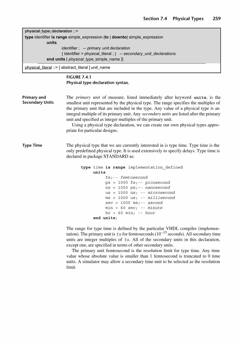
8/9/2019 VHDL for Engineers - Kenneth L. Short.pdf
http://slidepdf.com/reader/full/vhdl-for-engineers-kenneth-l-shortpdf 292/719
Section 7.4 Physical Types 259
Primary andSecondary Units
The primary unit of measure, listed immediately after keyword units, is thesmallest unit represented by the physical type. The range specifies the multiples of the primary unit that are included in the type. Any value of a physical type is an
integral multiple of its primary unit. Any secondary units are listed after the primaryunit and specified as integer multiples of the primary unit.Using a physical type declaration, we can create our own physical types appro-
priate for particular designs.
Type Time The physical type that we are currently interested in is type time. Type time is theonly predefined physical type. It is used extensively to specify delays. Type time isdeclared in package STANDARD as:
type time is range implementation_defined
units fs;-- femtosecond ps = 1000 fs;-- picosecond ns = 1000 ps;-- nanosecond us = 1000 ns; -- microsecond ms = 1000 us; -- millisecond sec = 1000 ms;-- second min = 60 sec; -- minute hr = 60 min; -- hour end units;
The range for type time is defined by the particular VHDL compiler (implemen-tation). The primary unit is fs for femtoseconds (10−15 seconds). All secondary timeunits are integer multiples of fs. All of the secondary units in this declaration,except one, are specified in terms of other secondary units.
The primary unit femtosecond is the resolution limit for type time. Any timevalue whose absolute value is smaller than 1 femtosecond is truncated to 0 timeunits. A simulator may allow a secondary time unit to be selected as the resolutionlimit.
physical_type_declaration ::=
type identifier is range simple_expression (to | downto) simple_expression
units
identifier ; -- primary unit declaration
{ identifier = physical_literal ; } -- secondary_unit_declarations
end units [ physical_type _simple_name ]]
physical_literal ::= [ abstract_literal ] unit _name
FIGURE 7.4.1
Physical type declaration syntax.

8/9/2019 VHDL for Engineers - Kenneth L. Short.pdf
http://slidepdf.com/reader/full/vhdl-for-engineers-kenneth-l-shortpdf 293/719
260 Chapter 7 Testbenches for Combinational Designs
SubtypeDelay_length
Package STANDARD also defines a subtype of time named delay_length:
subtype delay_length is time range
0 fs to time'high;
The range for the subtype delay_length is from 0 fs to the highest value of typetime.
Physical Literals Physical literals can be written as integral or nonintegral multiples of primary orsecondary units. If the value written is not an exact multiple of the primary unit, it isrounded down to the nearest multiple. Note that there must be a space before the unitname when physical values are written as literals.
ArithmeticOperations onPhysical Types
Arithmetic operators—addition, subtraction, identity, and negation—can be appliedto physical types. A value of a physical type can also be multiplied or divided by anumber of type integer or type real. All of the preceding operations yield a result of the same physical type. For example, assuming that constant prop_delay is typetime, we could write any of the following assignments:
s1 <= '0' after prop_delay * 2;s2 <= '1' after prop_delay / 4;
If two values of the same physical type are divided, the result is type integer. Directmultiplication of two physical types is not permitted, because the result would not bedimensionally correct. If two physical types must be multiplied, their values mustfirst be converted to abstract integers, these integers multiplied, and the result thenconverted to the final physical type. Examples of these types of operations are givenin Chapter 14.
7 .5 S ING LE P RO CE SS TE ST BE NC H
An easy approach to generating stimulus and checking responses uses a single
process testbench. Such a testbench includes a process that applies a stimulus to theUUT, waits an appropriate length of time, and then checks the UUT’s outputs. Theseactions are repeated until all stimulus values have been applied and all UUT outputsverified. The wait between applying each stimulus results in waveforms beinggenerated. Thus, the functionality of the stimulus generator and response monitor inFigure 7.1.1 are provided by the single process.
A single process testbench has two concurrent statements in its architecture body.One instantiates the UUT. The other is the process that applies the stimulus andverifies the UUT output values. Since the UUT instantiation and the process are bothconcurrent statements, either one can appear first in the architecture body. However,instantiation of the UUT first is the more common practice.

8/9/2019 VHDL for Engineers - Kenneth L. Short.pdf
http://slidepdf.com/reader/full/vhdl-for-engineers-kenneth-l-shortpdf 294/719
Section 7.5 Single Process Testbench 261
Single process testbenches differ in how the process generates or obtains eachstimulus value and determines the expected response. Some read test vectors from atable of constants in the testbench. Others execute algorithms that compute stimulusand expected output values during the simulation. Still others read test vectors froma file.
The testbench in Listing 1.5.1 used a process to apply each possible input combi-nation to a half adder over time and to check the half-adder’s outputs. This testbenchis repeated in Listing 7.5.1. Stimulus values and expected response values are simplywritten into the code as literals. The process is written without a sensitivity list. Waitstatements are used to realize a specific delay between the application of eachstimulus value. After the delay, an assertion statement checks the outputs.
LISTING 7.5.1Testbench for a half adder using a process to apply stimulus and assertion statementsto check outputs.
libraryieee;use ieee.std_logic_1164.all;
entity testbench is
end testbench;
architecture behavior of testbench is
-- Declare local signals to assign values to and to observe signal a_tb, b_tb, sum_tb, carry_out_tb : std_logic;
begin
-- Create an instance of the circuit to be tested uut: entity half_adder port map(a => a_tb, b => b_tb, sum => sum_tb, carry_out => carry_out_tb);
-- Define a process to apply input stimulus and verify outputs tb : process
constant period: time := 20 ns;
begin -- Apply every possible input combination
a_tb <= '0'; --apply input combination 00 and check outputs
b_tb <= '0'; wait for period; assert ((sum_tb = '0') and (carry_out_tb = '0')) report "test failed for input combination 00" severity error;
a_tb <= '0'; --apply input combination 01 and check outputs b_tb <= '1';
(Cont.)

8/9/2019 VHDL for Engineers - Kenneth L. Short.pdf
http://slidepdf.com/reader/full/vhdl-for-engineers-kenneth-l-shortpdf 295/719
262 Chapter 7 Testbenches for Combinational Designs
LISTING 7.5.1 (Cont.)
wait for period; assert ((sum_tb = '1') and (carry_out_tb = '0')) report "test failed for input combination 01" severity error;
a_tb <= '1'; --apply input combination 10 and check outputs b_tb <= '0'; wait for period; assert ((sum_tb = '1') and (carry_out_tb = '0')) report "test failed for input combination 10" severity error;
a_tb <= '1'; --apply input combination 11 and check outputs b_tb <= '1'; wait for period; assert ((sum_tb = '0') and (carry_out_tb = '1')) report "test failed for input combination 11" severity error;
wait; -- indefinitely suspend process
end process;end;
For example, the following statements assign a stimulus of all '0's to the UUTand check its outputs:
a_tb <= '0';
b_tb <= '0'; wait for period;assert ((sum_tb = '0') and (carry_out_tb = '0'))report "test failed for input combination 00" severity error;
Wait Statements ina Testbench
After a stimulus value is assigned to the half-adder’s inputs, a wait for statement isused to cause the simulator to wait for a time equal to the constant period. Thereare three reasons why this statement is required.
First, the signal assignments can’t take effect until after the process suspends.
Without the wait for statement, the response would be checked during the currentsimulation cycle and would not be the response to the newly assigned input values.
Second, waiting for a time interval allows the new input values to appear in thesimulator waveforms for this time period. This makes it possible to view thewaveform. Otherwise, all the actions in the process would take place in zerosimulation time. As a result, the waveform’s time axis would be compressed to zerolength and the waveforms would not be viewable.

8/9/2019 VHDL for Engineers - Kenneth L. Short.pdf
http://slidepdf.com/reader/full/vhdl-for-engineers-kenneth-l-shortpdf 296/719
Section 7.6 Wait Statements 263
Third, the wait for statements allow this same testbench to be used later, withoutmodification, for a timing simulation. For a timing simulation, the instantiated UUTis the timing model. During the simulation, we want the simulator to wait a period of time, determined from the design’s timing specification, before the UUT’s outputsare checked. The maximum propagation delay of the design mapped to the target
PLD must be less than or equal to this period of time, or the timing simulation fails.The final wait statement, without a for clause, suspends the process indefinitely.
This causes the simulation to stop. Without this final wait statement, the processwould repeat forever, or until the simulator time limit is reached.
AssertionStatements in aTestbench
Use of assertion statements eliminate the need to visually inspect timing waveforms.The condition in the first assertion statement requires that:
(sum_tb = '0') and (carry_out_tb = '0')
If this condition is true, the next statement in the process is executed. If it is false, the
message
"test failed for input combination 00"
is generated and severity level error is assigned. This message aids debugging bymaking it clear for which input combination the failure occurred.
The use of a wait statement to produce a delay between the application of eachstimulus, and the use of an assertion statement to automatically verify the UUT’sresponse, is common practice. Wait statements and assertion statements are examinedin detail in the next two sections, prior to our examining other testbench techniques.
7 . 6 WA I T ST A TE ME N TS
A wait statement suspends and resumes execution of the process containing thestatement. A wait statement can also appear in a procedure. A wait statement in aprocedure suspends and resumes the process that contains the call to the procedure.
Wait statements find widespread use in testbenches, but limited use in synthe-sizable code. The syntax for a wait statement is given in Figure 7.6.1.
As shown by its syntax, any combination of the three optional clauses (or nooptional clause) can be included in a wait statement. These clauses specify underwhat conditions the process resumes execution.
If only one, or none, of the optional clauses is included, four forms result:
wait on sensitivity_list; wait until boolean_expression; wait for time_expression; wait;

8/9/2019 VHDL for Engineers - Kenneth L. Short.pdf
http://slidepdf.com/reader/full/vhdl-for-engineers-kenneth-l-shortpdf 297/719

8/9/2019 VHDL for Engineers - Kenneth L. Short.pdf
http://slidepdf.com/reader/full/vhdl-for-engineers-kenneth-l-shortpdf 298/719
Section 7.7 Assertion and Report Statements 265
testbenches to delay for a time interval after a stimulus has been applied, beforechecking the UUT’s outputs. For example, the testbench of Listing 7.5.1 contains thefollowing wait for statement:
wait for period;
where period was a constant equal to 20 ns.
Multiple ConditionWait
A wait statement can contain all three clauses. For example, the statement
wait on ie until interrupt = '1' for period;
causes its process to resume when either ie changes value and interrupt = '1',or a time-out interval equal to period has expired, whichever occurs first.
Wait (Forever) The keyword wait by itself causes a process to suspend forever. We used this form
of wait statement at the end of Listing 7.5.1 to stop the testbench’s execution.
A Process as anInfinite Loop
A process with no wait statement or sensitivity list executes its statements insequence, starting at the first statement. After the last statement in the process isexecuted, the process immediately continues execution at its first statement, formingan infinite loop. As a result, the process never suspends.
Wait Statements inSynthesizable Code
Std 1076.6 2004 supports synthesis of all wait statements, except wait for state-ments. The earlier Std 1076.6 1999 only supported the wait until form for synthesis.Furthermore, Std 1076.6 1999 only allowed one wait until statement per process andit had to be the first statement in the process. An example of the use of a waitstatement for synthesis is given in Chapter 8 in the section “Using a Wait Statementto Infer a Flip-flop” on page 319.
7 .7 A SS ER TI ON A ND R EP OR T ST AT EM EN TS
The true power of a testbench is realized when it not only generates stimulus, butautomatically verifies output values. A process can check UUT output values againstexpected values. This is accomplished by placing assertion statements at appropriatepoints in the process. An assertion statement checks whether a specified condition(the assertion) is true. If it is not true, a message is displayed. This approach caneliminate the need to visually inspect simulator waveforms. The syntax rule for anassertion statement is given in Figure 7.7.1.
An assertion statement always has the required assert clause. The report andseverity clauses are optional. Note that an assertion statement is a single statementand only one semicolon is used, and must be at the very end of the statement.
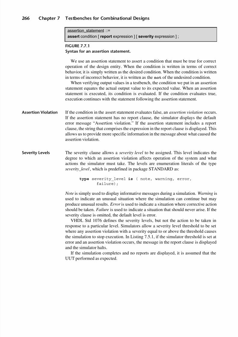
8/9/2019 VHDL for Engineers - Kenneth L. Short.pdf
http://slidepdf.com/reader/full/vhdl-for-engineers-kenneth-l-shortpdf 299/719
266 Chapter 7 Testbenches for Combinational Designs
We use an assertion statement to assert a condition that must be true for correctoperation of the design entity. When the condition is written in terms of correctbehavior, it is simply written as the desired condition. When the condition is writtenin terms of incorrect behavior, it is written as the not of the undesired condition.
When verifying output values in a testbench, the condition we put in an assertionstatement equates the actual output value to its expected value. When an assertionstatement is executed, its condition is evaluated. If the condition evaluates true,execution continues with the statement following the assertion statement.
Assertion Violation If the condition in the assert statement evaluates false, an assertion violation occurs.If the assertion statement has no report clause, the simulator displays the defaulterror message “Assertion violation.” If the assertion statement includes a reportclause, the string that comprises the expression in the report clause is displayed. Thisallows us to provide more specific information in the message about what caused theassertion violation.
Severity Levels The severity clause allows a severity level to be assigned. This level indicates thedegree to which an assertion violation affects operation of the system and whatactions the simulator must take. The levels are enumeration literals of the type
severity_level, which is predefined in package STANDARD as:
type severity_level is ( note, warning, error, failure);
Note is simply used to display informative messages during a simulation. Warning isused to indicate an unusual situation where the simulation can continue but mayproduce unusual results. Error is used to indicate a situation where corrective actionshould be taken. Failure is used to indicate a situation that should never arise. If theseverity clause is omitted, the default level is error.
VHDL Std 1076 defines the severity levels, but not the action to be taken in
response to a particular level. Simulators allow a severity level threshold to be setwhere any assertion violation with a severity equal to or above the threshold causesthe simulation to stop execution. In Listing 7.5.1, if the simulator threshold is set aterror and an assertion violation occurs, the message in the report clause is displayedand the simulator halts.
If the simulation completes and no reports are displayed, it is assumed that theUUT performed as expected.
assertion_statement ::=
assert condition [ report expression ] [ severity expression ] ;
FIGURE 7.7.1
Syntax for an assertion statement.

8/9/2019 VHDL for Engineers - Kenneth L. Short.pdf
http://slidepdf.com/reader/full/vhdl-for-engineers-kenneth-l-shortpdf 300/719
Section 7.7 Assertion and Report Statements 267
In using assertion statements to check outputs, we should place an assertionstatement in the process at each point where a new UUT output value is expected.The new expected value of the output is specified in the assertion condition. Aunique message should be provided in each assertion statement.
Report Statement In addition to the report clause in an assertion statement, there is a separate statementcalled a report statement. A report statement displays a message every time it isexecuted. If its severity clause is omitted, its severity level defaults to note (instead of error). Whenever executed, a report statement always generates the messageassociated with the report expression.
A report statement has the syntax given in Figure 7.7.2.
Report ClauseMessage Text
Report statements and report clauses in assertion statements only accept a singlestring. However, this string can be produced by concatenating substrings. The stringis displayed as a single line, unless the special character constants CR (carriage
return) and/or LF (line feed) are used in the concatenation of substrings. Forexample, the report statement
report "test failed" & CR LF & "for input combination 01" severity error;
will print the two lines:
test failedfor input combination 01
To aid in debugging, it is helpful if the string displayed by an assertion statementindicates the value of the input stimulus or other conditions that caused the assertionviolation. In Listing 7.5.1 it was not difficult to include the stimulus values asconstants in the report string. In general, we want to be able to display the actualvalue of the signal or variable associated with each assertion violation.
Image Attribute Values that appear in a report clause are not limited to literal values, but can be anexpression that is dynamically computed during simulation. Unfortunately, VHDLhas limited provisions for formatting types for display. For any scalar type, the image
attribute can be used to produce a string representation of the scalar type.
T’image(x) returns the string representation of the expression x of type T.
report_statement ::=
report expression [severity expression] ;
FIGURE 7.7.2
Syntax for a report statement.

8/9/2019 VHDL for Engineers - Kenneth L. Short.pdf
http://slidepdf.com/reader/full/vhdl-for-engineers-kenneth-l-shortpdf 301/719
268 Chapter 7 Testbenches for Combinational Designs
For example, the report statement
report "test failed for a_tb = " & std_logic’image(a_tb) & " and b_tb = " & std_logic’image(b_tb);
will display the values of a_tb and b_tb at the time that the statement is executed.For example, if the assertion violation occurs while a_tb equals '1' and b_tb
equals '0', the message displayed is:
test failed for a_tb = '1' and b_tb = '0'
To display values of composite data types, we must provide type conversionfunctions to convert the data types to formatted strings. This approach is discussedfurther in Chapter 12.
ConcurrentAssertionStatements
The assertion statements that we have seen in examples have been in processes andare, therefore, sequential statements. Assertion statements can also appear asconcurrent statements in an architecture body. A concurrent assertion statement isexecuted when one of the signals in its condition clause has an event. If the assertioncondition evaluates false, the report expression and severity expressions aredisplayed.
7 .8 R EC OR DS A ND TA BL E LO OK UP TE ST BE NC HE S
A simple way to specify both stimulus and expected response values is to use a tableof constants. This approach is similar to the table lookup technique used in Section4.9 to describe combinational designs.
When used in a testbench, table entries usually include both the input andoutput values of the combinational function’s truth table. Initial elements in a roware input values to be applied to the UUT. The remaining elements in that samerow are the corresponding expected output values. Each combination of inputvalues and corresponding expected output values (each row) in the table comprisesa test vector.
The testbench process reads each row in turn. Input values from a row are applied
to the UUT. Expected output values from the same row are compared to the UUT’soutputs.
Records A convenient way to represent a row of the table is as a record. A record is acomposite type that consists of named elements that may be of different types.Elements in a record are selected by name, not by an index number. The syntax for arecord declaration is given in Figure 7.8.1.

8/9/2019 VHDL for Engineers - Kenneth L. Short.pdf
http://slidepdf.com/reader/full/vhdl-for-engineers-kenneth-l-shortpdf 302/719
Section 7.8 Records and Table Lookup Testbenches 269
The identifiers of all the elements of a record type must be distinct. The value of a record object is the composite value of its elements.
Selected Names The entire value of a signal, variable, or constant record can be assigned to a signalor variable of the same record type using an assignment statement. When a singleelement of a record is to be selected for assignment to an object of the same element
type or a value is to be assigned to a single element of a record, that element’sselected name is used.A selected name consists of a prefix and a suffix separated by a period, as shown
in the syntax in Figure 7.8.2.For an element of a record, the prefix is the record name and the suffix is the
element name.
Test Vector Records Each test vector is defined as a record. This approach requires us to:
1. Declare a record type
2. Declare an array of records of the record type
3. Declare a constant of the array of records typeFor example, to declare a record for a test vector for the half adder we can write:
type test_vector is record
a : std_logic; b : std_logic; sum : std_logic; carry_out : std_logic;end record;
This record has four elements, all of which are type std_logic. The first two elements
are values for inputs a and b. The second two elements are the corresponding valuesfor outputs sum and carry_out.
record_declaration ::=
type identifier is record
identifier_list : element_subtype_definition ;
{ identifier_list : element_subtype_definition ; }
end record [ record_type _simple_name ]
FIGURE 7.8.1
Syntax for a record declaration.
selected_name ::=
prefix . suffix
FIGURE 7.8.2
Syntax for a selected name.

8/9/2019 VHDL for Engineers - Kenneth L. Short.pdf
http://slidepdf.com/reader/full/vhdl-for-engineers-kenneth-l-shortpdf 303/719
270 Chapter 7 Testbenches for Combinational Designs
The table of constants that comprises all of the test vectors is an array of recordsof type test_vector. This unconstrained array is declared as follows:
type test_vector_array is array
(natural range <>) of test_vector;
The actual table of constants, declared using named association, is
constant test_vectors : test_vector_array := (-- a, b, sum, carry_out(a => '0', b => '0', sum => '0', carry_out =>'0'),(a => '0', b => '1', sum => '1', carry_out =>'0'),(a => '1', b => '0', sum => '1', carry_out =>'0'),(a => '1', b => '1', sum => '0', carry_out =>'1'));
or more concisely, using positional association, is
constant test_vectors : test_vector_array := (-- a, b, sum, carry_out('0', '0', '0', '0'),('0', '1', '1', '0'),('1', '0', '1', '0'),('1', '1', '0', '1'));
The first two elements in each vector correspond to sequencing the inputs through allthe possible combinations required for an exhaustive verification. The second twoelements are the expected output values for those input values.
The complete testbench is given in Listing 7.8.1.
LISTING 7.8.1Table lookup testbench for a half adder.
library ieee;use ieee.std_logic_1164.all;
entity testbench is
end testbench;
architecture table of testbench is
-- Stimulus signalssignal a : std_logic;signal b : std_logic;-- Observed signalssignal sum : std_logic;signal carry_out : std_logic;

8/9/2019 VHDL for Engineers - Kenneth L. Short.pdf
http://slidepdf.com/reader/full/vhdl-for-engineers-kenneth-l-shortpdf 304/719
Section 7.8 Records and Table Lookup Testbenches 271
-- Declare record typetype test_vector is record
a : std_logic;b : std_logic;sum : std_logic;carry_out : std_logic;
end record;
type test_vector_array is array (natural range <>) of test_vector;
constant test_vectors : test_vector_array := (-- a, b, sum, carry_out('0', '0', '0', '0'),('0', '1', '1', '0'),('1', '0', '1', '0'),('1', '1', '0', '1'));
begin
UUT : entity half_adderport map (a => a, b => b, sum => sum, carry_out => carry_out );
verify : process
begin
for i in test_vectors'range loop
a <= test_vectors(i).a;b <= test_vectors(i).b;
wait for 20 ns;
assert (( sum = test_vectors(i).sum )and (carry_out = test_vectors(i).carry_out))
report "test vector " & integer'image(i) & " failed"&" for input a = " & std_logic'image(a)& " and b = " & std_logic'image(b)
severity error;end loop; wait;
end process;
end table;
In the declarative part of the architecture body, types test_vector andtest_vector_array are declared along with the constant test_vectors, asdescribed at the beginning of this section.
Following the UUT’s instantiation is the process verify that applies values tothe UUT’s inputs and verifies the UUT’s outputs.

8/9/2019 VHDL for Engineers - Kenneth L. Short.pdf
http://slidepdf.com/reader/full/vhdl-for-engineers-kenneth-l-shortpdf 305/719
272 Chapter 7 Testbenches for Combinational Designs
Looping ThroughInput Combinations
The statement part of the process consists primarily of a single for loop. The loop’sindex range corresponds to the range of the constant test_vectors. In thisexample, that range is from 0 through 3, since there are four rows in tabletest_vectors.
Each time through the loop, the input values from a test vector determined by the
loop index are assigned to the inputs of the UUT, using the selected names of theelements in the record:
a <= test_vectors(i).a;b <= test_vectors(i).b;
After a wait of 20 ns, the assertion statement checks whether the UUT’s outputs havethe expected values, as specified by the test vector. If either UUT output is not equalto its expected value, then the message “test vector n failed” is displayed by thesimulator.
The report clause uses the predefined image attribute, integer'image(i), toconvert the loop index to a string equal to the index value, so that the index of thespecific test vector that failed can be displayed. It also uses the image attribute toprint the values of a and b for test vectors that failed. For example, if the fourth testvector (with index 3) fails, the message output is:
test vector 3 failed for input a = '1' and b = '1'
In this example, the vector index and values for a and b in the report clause provideredundant information; only one is really needed.
The loop repeats until all test vectors from the table have been processed.
7 .9 TE ST BE NC HE S T H AT CO MP UT E S TI MU LU S AN D E XPE C TE D RE SULTS
In previous testbenches, expected output values were predetermined for each inputcombination and included in the testbench as literals. Alternatively, a testbench canbe written so that the expected output values are computed during the simulation. Ina single process testbench, the same process is used to apply stimulus and compute
and verify expected results.Listing 7.9.1 is a testbench for the half adder that computes the expected results.This testbench differs from the one in Listing 7.5.1 only in its process. In the
beginning of the process, a constant n is defined that is equal to the number of UUTinputs. A for loop, whose index value ranges from 0 to 2n − 1, is then used. Theexponentiation operator symbol is the double asterisk (**). Inside the for loop, thefunction to_unsigned is used to convert the integer index value to an unsigned

8/9/2019 VHDL for Engineers - Kenneth L. Short.pdf
http://slidepdf.com/reader/full/vhdl-for-engineers-kenneth-l-shortpdf 306/719
Section 7.9 Testbenches That Compute Stimulus and Expected Results 273
LISTING 7.9.1Half-adder testbench that computes expected results.
library ieee;use ieee.std_logic_1164.all;use ieee.numeric_std.all;
entity testbench is
end testbench;
architecture behavior of testbench is
-- Declare signals to assign values to and to observesignal a_tb, b_tb, sum_tb, carry_out_tb : std_logic;
begin
-- Create an instance of the circuit to be tested uut: entity half_adder port map(a => a_tb, b => b_tb,
sum => sum_tb, carry_out => carry_out_tb);
-- Define a process to apply input stimulus and test outputstb : process
constant period: time := 20 ns;constant n: integer := 2;
begin -- Apply every possible input combinationfor i in 0 to 2**n - 1 loop
(a_tb, b_tb) <= to_unsigned(i,n); wait for period;assert ((sum_tb = (a_tb xor b_tb)) and (carry_out_tb = (a_tb and b_tb))
)report "test failed" severity error;
end loop; wait; -- indefinitely suspend process
end process;end;
vector of length n. The value of this vector is then assigned to the aggregate formedfrom the UUT’s inputs (a_tb, b_tb):
(a_tb, b_tb) <= to_unsigned(i,n);
Using Functionto_unsigned toGenerate Stimulus
Function to_unsigned was previously introduced in the subsection “Functions forConversion to and from Type Integer” on page 109. Recall that this function has twoparameters. The first parameter is the integer to be converted. The second is thelength of the returned unsigned vector. This vector’s element values are the binaryequivalent of the integer value passed to the function.
In the previous assignment statement, the unsigned vector value returned by theto_unsigned function is assigned to an aggregate made up of the scalar input

8/9/2019 VHDL for Engineers - Kenneth L. Short.pdf
http://slidepdf.com/reader/full/vhdl-for-engineers-kenneth-l-shortpdf 307/719
274 Chapter 7 Testbenches for Combinational Designs
signals. Since each of these scalar inputs is type std_logic and the elements of anunsigned vector are also type std_logic, the assignment is valid.
We will often use the function to_unsigned inside a loop in a testbench to applyall possible input combinations to a UUT. The package NUMERIC_STD and typeunsigned are discussed in more detail in Chapter 13.
After waiting for an interval of time, the UUT’s outputs are checked. Theexpected values are computed from the input values using Boolean expressions. Thecondition in the assertion requires that the expressions
sum_tb = (a_tb xor b_tb)
and
carry_out_tb = (a_tb and b_tb)
evaluate true for the assertion to be valid.
Using a loop, a conversion function, and Boolean expressions to compute theoutput leads to a more concise testbench.When the preceding testbench is used for functional verification of a half adder
whose architecture is behavioral style or structural style, it is very effective. But, if this testbench is used for functional verification of a dataflow style half adder whosearchitecture uses the same equations, it is not at all effective, because we are simplyverifying the Boolean expressions against themselves.
However, if the UUT is the synthesized logic for the dataflow style half adder, thespecific logic primitives of the hardware implementation are not usually identical tothose of the equations and the testbench again provides an effective verification.
The computation of expected results can also be done using a process separate
from the one that generates stimulus. This separate process may simply be an intentmodel. We will see an example of this in Section 7.12, after shift operators are intro-duced in the next section.
7 . 1 0 P R E D EF I N ED SH I F T O P E R AT O R S
In addition to its logical operators, VHDL provides a number of shift and rotateoperators. The shift and rotate operators are collectively called shifts, and are definedin package STANDARD for one-dimensional arrays whose elements are either of
type bit or type boolean, Table 7.10.1.The operators in Table 7.10.1 are not overloaded for std_ulogic operands in
package STD_LOGIC_1164, as VHDL’s logical operators are. So, we cannot usethem on type std_logic_vector. Package NUMERIC_STD does overload theseoperators for types unsigned and signed, and these types can be used when we wantto synthesize these operatons.

8/9/2019 VHDL for Engineers - Kenneth L. Short.pdf
http://slidepdf.com/reader/full/vhdl-for-engineers-kenneth-l-shortpdf 308/719
Section 7.10 Predefined Shift Operators 275
However, as we shall see, the predefined shift operators using type bit operandscan be very useful in testbenches. Accordingly, they are discussed here.
Logical Shifts The left operand for each operator must be a one-dimensional array, either a bitvector or boolean vector. The right operand must be an integer. For bit vectors,logical shifts shift the bit vector n positions in the direction specified by the rightoperand. n '0's are shifted in, where n is the value of the integer. The bits shifted outare discarded. If n is a negative integer, the direction of the shift is opposite of thatspecified by the operator. For example:
b"10101101" sll 3 = b"01101000"
b"10101101" sll -3 = b"00010101"
For boolean vectors, false is shifted in instead of '0'.
Arithmetic Shifts For arithmetic shifts, a copy of the bit in the original operand at the end opposite thedirection of shift is shifted in. For example. for shift right arithmetic, a copy of theleftmost bit is shifted in:
b"10101101" sra 2 = b"11101011"
For a shift right arithmetic operation this preserves the sign bit, assuming the bitvector is interpreted as a two’s complement number. Arithmetic shifts are commonin the assembly language instruction sets of computers.
In assembly language, there is no distinction between a shift left arithmeticoperation and a shift left logical operation. In contrast, in VHDL a shift left arithmeticoperation shifts in a copy of the rightmost bit of the original operand. For example:
b"10101101" sla 2 = b"10110111"
Table 7.10.1VHDL shift operators.
Operator Description
sll shift left logical
srl shift right logical
sla shift left arithmetic
sra shift right arithmetic
rol rotate left logical
ror rotate right logical

8/9/2019 VHDL for Engineers - Kenneth L. Short.pdf
http://slidepdf.com/reader/full/vhdl-for-engineers-kenneth-l-shortpdf 309/719
276 Chapter 7 Testbenches for Combinational Designs
Rotates The ror and rol rotate operations are similar to the srl and sll shift operations,except the bit rotated out of one end of the vector is rotated into the other end.
The shift operators defined in package STANDARD cannot be applied directly tostd_logic_vectors. However, by using type conversion functions we can use shiftoperators with std_logic_vector signals. An example of this is given in the next section.
7 . 11 S T IM UL U S O RD ER B A S ED O N U U T F U N C T I O N A L I TY
In previous testbenches the stimulus values were applied by aggregating all inputs into asingle vector and counting this vector through all of its possible values starting from 0.It is often preferable, particularly for more complex combinational systems, to applystimulus values in an order that is related to the functionality of the UUT. That is, values
are applied to certain UUT control inputs to put the UUT in a particular mode of operation. Other inputs are then sequenced through all of their values. This verifies eachdifferent mode of operation of the UUT in a logical fashion. While this may lead to atextually longer stimulus process, it is often more readable and understandable to others.
For example, consider the 74F539 design “Example of a 74F539 Decoder Equiv-alent” on page 175. Using the truth table in Table 5.4.1 as the specification of thedesign’s functionality, we might first make oe_bar = 1, which should cause allUUT’s outputs to be high impedance (Z), independent of any other input’s value.Then we could sequence all the other inputs through every combination, verifyingthat each output is Z for all combinations of these inputs.
Next, the stimulus process could then make oe_bar = 0 and e_bar = 1 and verify
that the decoder functionality is not enabled and that all outputs should be equal toinput p.
Finally, the stimulus process could make e_bar = 0, enabling the decoder andcausing the output selected by a to be the complement of p and all other outputsequal to p. Input a would then be sequenced through all of its possible values.
Each part of the stimulus process would be documented to indicate exactly whataspect of the decoder’s functionality was being verified by that part. A testbench thatfollows this approach is given in Listing 7.11.1.
LISTING 7.11.1
Testbench for ic74f539 with stimulus application order based on UUT functionality.
library ieee;use ieee.numeric_std.all;use ieee.std_logic_1164.all;
entity ic74f539_tb is
end ic74f539_tb;

8/9/2019 VHDL for Engineers - Kenneth L. Short.pdf
http://slidepdf.com/reader/full/vhdl-for-engineers-kenneth-l-shortpdf 310/719

8/9/2019 VHDL for Engineers - Kenneth L. Short.pdf
http://slidepdf.com/reader/full/vhdl-for-engineers-kenneth-l-shortpdf 311/719
278 Chapter 7 Testbenches for Combinational Designs
LISTING 7.11.1 (Cont.)
o_exp := (p & p & p & p) xor
to_stdlogicvector("0001" rol to_integer(unsigned(a)));assert (o = o_exp)report "enable asserted failed" severity error;
end loop; wait;
end process;
end tb_architecture;
In the stimulus process, a variable o_exp is used to hold the computed expectedoutput value that is compared to the actual output value o.
There are two type conflicts that must be resolved to use the rol operator. First,
the right operand of a rol operator must be an integer, but a is a std_logic_vector. Toeliminate this type conflict, a is first converted to unsigned. Function to_integer
is then used to convert the unsigned value to an integer.
Converting aBit_vector to aStd_logic_vector
The result of a rol operation is a bit_vector. In this example, the result must be assignedto a std_logic_vector. To eliminate this second type conflict, the function to_stdlogicvector, from package STD_LOGIC_1164, is used. Function to_stdlogicvector
converts a bit_vector to a std_logic_vector.
Verifying Don’tCare Output Values
Stimulus application ordered by UUT functionality is also useful when a combina-tional system has some outputs that are defined as don’t cares for certain input(stimulus) values. For example, when verifying the outputs of a BCD to seven-segment decoder, we would separate the stimulus into two sets: one for valid inputsand the other for invalid inputs (those assigned don’t care output values). We wouldneed two different testbenches, one for functional simulation and another for post-sythesis and timing simulation.
The testbench for functional simulation would use two loops, one to apply thevalid inputs and the other to apply the invalid inputs. The first loop would check forthe expected decoder output values. The second loop would check for all outputsbeing '-'. It is important that we verify the '-' outputs for inputs corresponding tothe second loop, because we want the synthesizer to be able to take advantage of these don’t cares to simplify the logic.
The testbench for post-sythesis and timing simulation would be the same as thefirst testbench, except that it would not include the second loop. We don’t want toverify the outputs from the synthesized logic corresponding to invalid inputs,because we don’t know or care what those values will be.
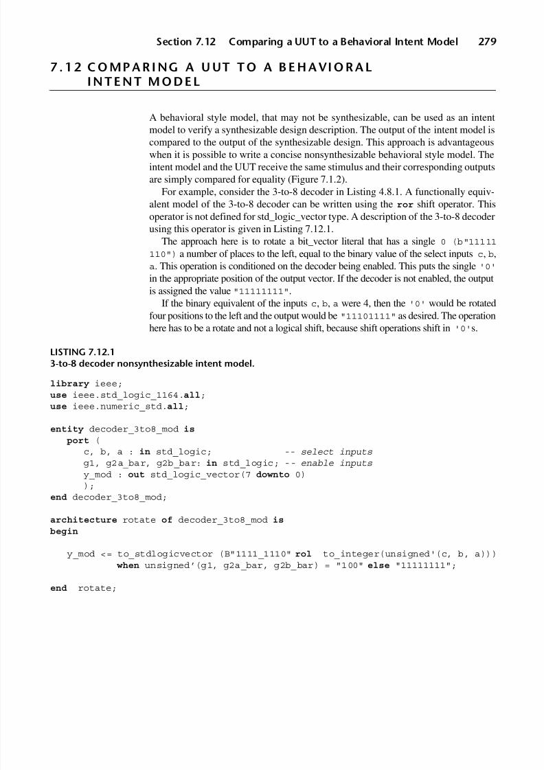
8/9/2019 VHDL for Engineers - Kenneth L. Short.pdf
http://slidepdf.com/reader/full/vhdl-for-engineers-kenneth-l-shortpdf 312/719
Section 7.12 Comparing a UUT to a Behavioral Intent Model 279
7 . 1 2 C O MP A R I NG A U UT T O A B E H A VI O R A L I N T E N T M O D E L
A behavioral style model, that may not be synthesizable, can be used as an intent
model to verify a synthesizable design description. The output of the intent model iscompared to the output of the synthesizable design. This approach is advantageouswhen it is possible to write a concise nonsynthesizable behavioral style model. Theintent model and the UUT receive the same stimulus and their corresponding outputsare simply compared for equality (Figure 7.1.2).
For example, consider the 3-to-8 decoder in Listing 4.8.1. A functionally equiv-alent model of the 3-to-8 decoder can be written using the ror shift operator. Thisoperator is not defined for std_logic_vector type. A description of the 3-to-8 decoderusing this operator is given in Listing 7.12.1.
The approach here is to rotate a bit_vector literal that has a single 0 (b"11111
110") a number of places to the left, equal to the binary value of the select inputs c, b,a. This operation is conditioned on the decoder being enabled. This puts the single '0'in the appropriate position of the output vector. If the decoder is not enabled, the outputis assigned the value "11111111".
If the binary equivalent of the inputs c, b, a were 4, then the '0' would be rotatedfour positions to the left and the output would be "11101111" as desired. The operationhere has to be a rotate and not a logical shift, because shift operations shift in '0's.
LISTING 7.12.13-to-8 decoder nonsynthesizable intent model.
library ieee;use ieee.std_logic_1164.all;use ieee.numeric_std.all;
entity decoder_3to8_mod is
port ( c, b, a : in std_logic; -- select inputs g1, g2a_bar, g2b_bar: in std_logic; -- enable inputs y_mod : out std_logic_vector(7 downto 0) );end decoder_3to8_mod;
architecture rotate of decoder_3to8_mod isbegin
y_mod <= to_stdlogicvector (B"1111_1110" rol to_integer(unsigned'(c, b, a))) when unsigned’(g1, g2a_bar, g2b_bar) = "100" else "11111111";
end rotate;

8/9/2019 VHDL for Engineers - Kenneth L. Short.pdf
http://slidepdf.com/reader/full/vhdl-for-engineers-kenneth-l-shortpdf 313/719
280 Chapter 7 Testbenches for Combinational Designs
There are two type conflicts that must be resolved to use the rol operator. First,the right operand of a rol operator must be an integer, but c, b, a is an aggregate. Toeliminate this type conflict, the aggregate is first type qualified as unsigned. Functionto_integer is then used to convert the unsigned value to an integer.
The result of a rol operation is a bit_vector. In this example, the result must be
assigned to a std_logic_vector. To eliminate this second type conflict, the functionto_stdlogicvector, from package STD_LOGIC_1164, is used.
The testbench is given in Listing 7.12.2.
LISTING 7.12.2A testbench that compares the outputs of two models.
library ieee;use ieee.std_logic_1164.all;use ieee.numeric_std.all;
entity decoder_3to8_tb is
end decoder_3to8_tb;
architecture tb_architecture of decoder_3to8_tb is
-- Stimulus signalssignal c : std_logic;signal b : std_logic;signal a : std_logic;signal g1 : std_logic;signal g2a_bar : std_logic;signal g2b_bar : std_logic;
-- Observed signalssignal y : std_logic_vector(7 downto 0);signal y_mod : std_logic_vector(7 downto 0);
begin
-- Unit Under Test port mapUUT : entity decoder_3to8 port map (c => c, b => b, a => a,
g1 => g1, g2a_bar => g2a_bar, g2b_bar => g2b_bar, y => y );
-- Behavioral Model port mapUMOD : entity decoder_3to8_mod port map (c => c, b => b, a => a,
g1 => g1, g2a_bar => g2a_bar,g2b_bar => g2b_bar, y_mod => y_mod );
-- Stimulus and verification processtb: process
constant period : time := 100 ns;begin
for i in 0 to 63 loop
(c, b, a, g1, g2a_bar, g2b_bar) <= std_logic_vector(to_unsigned(i, 6));

8/9/2019 VHDL for Engineers - Kenneth L. Short.pdf
http://slidepdf.com/reader/full/vhdl-for-engineers-kenneth-l-shortpdf 314/719
Section 7.13 Code Coverage and Branch Coverage 281
wait for period;assert y = y_modreport "error for input vector " & integer'image(i)severity error;
end loop; wait;
end process;end tb_architecture;
In the statement part of the architecture body there are three concurrent state-ments. Two are the instantiations of the components UUT and UMOD, where UMOD isthe intent model. The third is the process that provides the stimulus and verifies theoutputs. The loop inside this process applies each possible input combination simul-taneously to both UUT and UMOD. An assert statement compares output vectors y andy_mod from UUT and UMOD, respectively, for each input combination. If—for anycombination—they are not equal, an error is reported.
7 . 1 3 C O D E CO V E RA G E A ND B R A NC H C O VE R A GE
When developing a testbench to functionally verify a design, we would like to knowthe effectiveness of the verification. We have seen that, for combinational designs, itis not difficult to create a testbench that applies all possible input combinations. Wewill see later, in Chapters 14 and 15, that for complex sequential designs, exhaustiveverification is usually impractical.
Code CoverageTool
A software tool that is very helpful in evaluating testbench effectiveness is a codecoverage tool. A code coverage tool is a program that allows us to determine whatsource code is executed during a simulation. While the simulation is running, thecode coverage tool gathers information about how many times each statement isexecuted. When the simulation is complete, this information can be displayed. Wecan obtain code coverage information on the UUT, all of its subcomponents, and thetestbench itself.
We can use code coverage to determine whether our testbench causes all of thestatements in a design description (UUT) to be executed. If it does not, we candetermine how the testbench should be modified to achieve 100% code coverage for
the UUT.While our half adder and its testbench are so simple that they do not require the
use of code coverage, they can be used to illustrate some of the basic capabilitiesprovided by such a tool.
After completion of the execution of the testbench in Listing 7.5.1 we can openthe code coverage viewer to see the code coverage results. The Hierarchy panedisplays the hierarchical structure of the testbench (Figure 7.13.1). At the root of the

8/9/2019 VHDL for Engineers - Kenneth L. Short.pdf
http://slidepdf.com/reader/full/vhdl-for-engineers-kenneth-l-shortpdf 315/719
282 Chapter 7 Testbenches for Combinational Designs
hierarchy tree is the testbench itself and its process tb. Beneath the root we have theinstantiation of the UUT. Within the UUT we have two simulation processesassociated with the two concurrent signal assignment statements in the architecturebody.
Code Coverage as aMetric Code coverage is the ratio of the number of statements executed to the total numberof executable statements, expressed as a percentage. As seen from Figure 7.13.1(CC[%] column), the code coverage for each simulation process in the UUT is 100%and, therefore, the code coverage for the UUT is 100%.
When an instance name in the hierarchy pane is selected, its source code isdisplayed. This provides further details of the code coverage. With the UUTselected, the source code in Figure 7.13.2 is displayed.
We can see from this figure that each concurrent signal assignment statement isexecuted five times. We might have expected that each statement would be executedonly four times, since the testbench only applies the four possible binary combina-tions of two inputs. However, the first execution of these statements is not due to the
application of a binary input combination by the testbench, but rather is theexecution caused by the initialization phase of the simulation.
FIGURE 7.13.1
Hierarchy window of code coverage viewer.
FIGURE 7.13.2
Code coverage view of source code for half adder.
hadder.vhd
Line Count BC Source
123456789
10111213141516
NoneNoneNoneNoneNoneNoneNoneNoneNone
NoneNone55NoneNoneNone
Details
–– c:\bkvhdl_progs\Chap01\half_adder\src\hadder.vhd
library ieee;use ieee.std_logic_1164.all;
entity half_adder is port (a, b : in std_logic; sum, carry_out: out std_logic);end half_adder;
architecture dataflow of half_adder is begin sum <= a xor b; carry_out <= a and b;end dataflow.

8/9/2019 VHDL for Engineers - Kenneth L. Short.pdf
http://slidepdf.com/reader/full/vhdl-for-engineers-kenneth-l-shortpdf 316/719
Section 7.13 Code Coverage and Branch Coverage 283
The testbench itself is indicated in Figure 7.13.1 as having 94.44% coverage (17of its 18 instructions were executed). If the testbench is selected in the Hierarchypane, its source code is displayed (Figure 7.13.3). From this figure it can be seen thatthe end process statement is not executed because of the last wait statement.
Though not readily discernible in Figures 7.13.2 and 7.13.3, this code coverage
tool uses color coding to indicate which statements were executed. Executed state-ments have a green background. Statements that were not executed have a redbackground. Nonexecutable statements have a gray background.
FIGURE 7.13.3
Code coverage view of half-adder testbench.
half_adder_tb.vhd
Line Count BC Source
12345678
91011121314151617181920212223242526
272829303132333435363738394041424344
45464748495051
NoneNoneNoneNoneNoneNoneNoneNone
NoneNoneNoneNoneNoneNoneNoneNoneNoneNoneNoneNoneNoneNoneNoneNone11
11NoneNone1111NoneNone1111NoneNone11
11NoneNone10None
Details
–– c:\kls\Bkvhdl_progs\Chap01\half_adder\src\half_adder_tb.vhd
library ieee;use ieee.std_logic_1164.all;
entity testbench isend testbench;
architecture behavior of testbench is
–– Declare signals to assign values to and observe signal a_tb, b_tb, sum_tb, carry_out_tb : std_logic;
begin –– Create an instance of the circuit to be tested uut: entity half_adder port map(a => a_tb, b => b_tb, sum => sum_tb, carry_out => carry_out_tb);
–– Define a process to apply input stimulus and test outputs tb : process constant period: time : = 20 ns;
begin –– Apply every possible input combination
a_tb <= '0'; ––apply input combination 00 and check outputs b_tb <= '0';
wait for period; assert ((sum_tb = '0') and (carry_out_tb = '0')) report "test failed for input combination 00" severity error;
a_tb <= '0'; ––apply input combination 01 and check outputs b_tb <= '1'; wait for period; assert ((sum_tb = '1') and (carry_out_tb = '0')) report "test failed for input combination 01" severity error;
a_tb <= '1'; ––apply input combination 10 and check outputs b_tb <= '0'; wait for period; assert ((sum_tb = '1') and (carry_out_tb = '0')) report "test failed for input combination 10" severity error;
a_tb <= '1'; ––apply input combination 11 and check outputs b_tb <= '1';
wait for period; assert ((sum_tb = '0') and (carry_out_tb = '1')) report "test failed for input combination 11" severity error;
wait; –– indefinitely suspend process end process;end;

8/9/2019 VHDL for Engineers - Kenneth L. Short.pdf
http://slidepdf.com/reader/full/vhdl-for-engineers-kenneth-l-shortpdf 317/719

8/9/2019 VHDL for Engineers - Kenneth L. Short.pdf
http://slidepdf.com/reader/full/vhdl-for-engineers-kenneth-l-shortpdf 318/719
Section 7.14 Post-Synthesis and Timing Verifications for Combinational Designs 285
simply replace the design description as the UUT with the post-synthesis VHDLmodel.
Since the post-synthesis model does not include delays and since the purpose of post-synthesis verification is to verify that the synthesizer has successfully translateda design description to gate-level logic, use of the same testbench used for functional
verification is appropriate.If functional verification of the post-synthesis model is skipped, verification of
the synthesized logic can be accomplished as part of the timing verification. If thedelay between application of each stimulus and verification of the correspondingUUT outputs was appropriately chosen when the functional verification testbenchwas originally written, this testbench may be directly usable for the timing verifi-cation. However, it may be preferable to modify this testbench by adding assertionstatements to automatically verify the UUT’s timing.
Hazards in
CombinationalCircuits
Before considering use of assertion statements to verify timing performance, it is
important to consider hazards in combinational circuits. A hazard is an output glitchcaused by the gate-level structure of a circuit and the propagation delays of itsindividual gates.
Static Hazard A static hazard occurs when a change in the input values to a combinational circuitcauses an output to briefly change value when functionally it should have remainedthe same. This brief change (glitch) is caused by differences in propagation delaysthrough different signal paths in the circuit. Static hazards are illustrated in Figure7.14.1(a) and (b).
A static 0 hazard occurs when an output that should remain a 0 briefly transitions
to a 1 in response to an input change. A static 1 hazard occurs when an output thatshould remain a 1 briefly transitions to a 0.
Dynamic Hazard A dynamic hazard occurs when a change in the input values to a combinationalcircuit causes an output to briefly change value multiple times when it should have
FIGURE 7.14.1
Static and dynamic hazards: (a) static 0 hazard, (b) static 1 hazard, (c) dynamic0 hazard, and (d) dynamic 1 hazard.
0
1
0
1
0
1
0
1
(a) (b)
(c) (d)

8/9/2019 VHDL for Engineers - Kenneth L. Short.pdf
http://slidepdf.com/reader/full/vhdl-for-engineers-kenneth-l-shortpdf 319/719
286 Chapter 7 Testbenches for Combinational Designs
changed value only once (Figure 7.14.1(c) and (d)). A dynamic 0 hazard resultswhen, instead of a single transition from 1 to 0, there are multiple transitions. Adynamic 1 hazard results when, instead of a single transition from 0 to 1, there aremultiple transitions.
Hazards inFunctional andPost-synthesisSimulations
We have seen that functional simulation of the circuit in Figure 6.8.3 shows a static1 hazard when the input is changed from 0 to 1. This hazard can be seen duringfunctional simulation because the simulator associates a δ delay with each gate in thecircuit and the propagation delays of the two signal paths from the circuit’s input tothe inputs of the NAND gate differ by 1 δ. Because of this difference, a hazard of 1 δduration occurs.
The duration of a hazard in a functional or post-synthesis simulation is one ormore δs and does not extend beyond the time step. Since we verify the UUT’soutputs after a delay that is much greater than the duration of the hazard, the hazardnever causes an incorrect value to be seen by an assertion statement.
Hazards in TimingSimulations
In a timing model, the gate delays and propagation delays of signal paths are those of the logic mapped to the target PLD. These delays are relatively significant and theduration of any hazards will be for corresponding magnitudes of time.
Two Pass Logic In SPLDs of limited logic capacity, the place-and-route tool may feed an output back to one of the SPLD’s inputs to provide the additional logic required to realize aparticular Boolean expression. This second pass through a SPLD can result in statichazards having durations comparable to the propagation delay of the SPLD.
When visually verifying the output of the timing model of a combinationalsystem, we may see output values that are “incorrect” for significant periods of timedue to hazards.
Hazard Free Design In traditional digital design, when a hazard free circuit is desired, we can modify thedesign to achieve this objective. This is typically done using a Karnaugh map andadding implicants so that any two adjacent 1s in the map are covered by the sameimplicant. This corresponds to adding terms to the sum-of-products expression forthe function. The result is to add gates (hazard-suppressing logic) to the circuit. Thisproduces a circuit that is not minimal cost.
Synthesis tools do not produce hazard free designs. If we start with a hazard freedescription, the synthesis tool will likely remove the redundant terms in the sum-of-products expression during optimization. This removes the hazard-suppressing logicand the remaining logic is not hazard free.
Creating circuits with hazards is usually a problem only if we are implementingasynchronous sequential systems. However, in this book, when designing sequentialsystems our interests are limited to synchronous systems.

8/9/2019 VHDL for Engineers - Kenneth L. Short.pdf
http://slidepdf.com/reader/full/vhdl-for-engineers-kenneth-l-shortpdf 320/719
Section 7.14 Post-Synthesis and Timing Verifications for Combinational Designs 287
Using Assertions toVerify Timing inCombinationalSystems
When using assertions statements to verify timing, we must consider the possibilityof hazards affecting the verification. For a timing simulation, we must verify theUUT’s outputs at the time that they are required by the system’s specification to bestable with their new values. After we do this, we need to verify that the outputvalues do not subsequently change as the result of a hazard.
The testbench process in Listing 7.9.1 is modified to verify a half-adder’s timingin Listing 7.14.1.
In this process, the time between each application of stimulus is given by theconstant period. The maximum allowed propagation delay, taken from the system’sspecification, is given by the constant tpd_spec.
After a new stimulus is applied, the process suspends for tpd_spec. When theprocess resumes, it uses an assertion statement to verify the UUT’s output values.The process then suspends for a time equal to period - tpd_spec.
LISTING 7.14.1Process to verify logic and timing of half-adder timing model.
tb : process
constant tpd_spec : time := 11 ns;constant period: time := 20 ns;constant n: integer := 2;
begin
-- Apply every possible input combinationfor i in 0 to 2**n - 1 loop
(a_tb,b_tb) <= to_unsigned(i,n);
-- Verify output values at specified time wait for tpd_spec;assert ((sum_tb = (a_tb xor b_tb))
and (carry_out_tb = (a_tb and b_tb)))report "test failed for a_tb = " & std_logic'image(a_tb)& " and b_tb = " & std_logic'image(b_tb)severity error;
-- Verify that outputs do not subsequently chnage Wait for period - tpd_spec;assert sum_tb'quiet(period - tpd_spec)
and carry_out_tb'quiet(period - tpd_spec)
report "propagation delay specification exceded"severity error;
end loop; wait;
end process;end;

8/9/2019 VHDL for Engineers - Kenneth L. Short.pdf
http://slidepdf.com/reader/full/vhdl-for-engineers-kenneth-l-shortpdf 321/719
288 Chapter 7 Testbenches for Combinational Designs
Signal AttributeQuiet
When the process again resumes, it verifies that the outputs have not changed sincethey were last verified. This is accomplished using the signal attribute quiet. Recallthat attribute quiet creates an implicit signal that has a boolean value of true only
if no transactions have occurred on its associated signal for the specified time up tothe current time.
Implicit signals created by signal attributes can be displayed in waveforms. Theimplicit signals created by the process in Listing 7.14.1 can be seen in Figure 7.14.2.
7 . 1 5 T I MI N G M OD E L S U SI N G V I TA L A N D S D F
Timing Model To perform a timing simulation, the UUT must be the timing model automaticallygenerated by the place-and-route tool. This is a structural VHDL netlist thatdescribes how components, which are primitives of the target PLD architecture, areinterconnected to implement the design.
A SPLD timing model may include specification of timing delays within theVHDL netlist description. More commonly for CPLDs and FPGAs, the timingmodel consists of two files. One is a delayless structural VHDL netlist and the otheris a non-VHDL text file that contains timing delay information for each componentinstance in the netlist.
Timing Model for aSPLD
The architecture of a SPLD is relatively simple. As a result, it’s fairly easy to createits timing model. Interconnect paths in a SPLD are relatively short and of similarlengths. The associated interconnect path delays are insignificant relative to thedelays of the component primitives.
Generics Generics allow a design entity to be described so that, for each use of the designentity, its structure and/or behavior can be altered by the choice of generic values.Generics can be any type, but most often are types integer, boolean, or time.
FIGURE 7.14.2
Timing waveforms showing implicit signals created by quiet attributes.

8/9/2019 VHDL for Engineers - Kenneth L. Short.pdf
http://slidepdf.com/reader/full/vhdl-for-engineers-kenneth-l-shortpdf 322/719
Section 7.15 Timing Models Using VITAL and SDF 289
Generics are similar to constants, except their default values can be overriddenfrom outside of the design entity in which they are declared. Default generic valuesfor a design entity are specified inside its entity declaration. If not overridden, these
values apply. Default values can be overridden from outside of the design entity ineither:
• The component instantiation statement that instantiates the design entity
• A configuration declaration.
Generic Clause Generics are declared in a formal generic clause in an entity declaration. Anexpanded syntax for an entity declaration is given in Figure 7.15.1. When genericsare used, the generic clause precedes the port clause.
Once declared, a generic can be used in the entity declaration itself and in all
architectures associated with the entity.
Generics in aTiming Model
A timing model may make use of generics to specify delay times. As a very simpleexample, a description of a trivial timing model for a half-adder design is given inListing 7.15.1. For simplicity, this model uses concurrent signal assignment state-ments rather than component instantiation statements.
LISTING 7.15.1Trivial timing model for a half adder.
library ieee;use ieee.std_logic_1164.all;
entity half_adder is
generic ( tpd : time := 10 ns);port (a, b : in std_logic; sum, carry_out: out std_logic);
end half_adder;(Cont.)
entity_declaration ::=
entity identifier is
[ generic ( generic _interface_list ) ; ]
[ port ( port _interface_list ) ; ]
end [ entity ] [ entity _simple_name ] ;
generic _interface_list ::=
[ constant ] identifier_list : [ in ] subtype_indication [ := static _expression ]
{[ constant ] identifier_list : [ in ] subtype_indication [ := static _expression ]}
FIGURE 7.15.1
Expanded syntax for an entity declaration that includes a formal generic clause.

8/9/2019 VHDL for Engineers - Kenneth L. Short.pdf
http://slidepdf.com/reader/full/vhdl-for-engineers-kenneth-l-shortpdf 323/719
8/9/2019 VHDL for Engineers - Kenneth L. Short.pdf
http://slidepdf.com/reader/full/vhdl-for-engineers-kenneth-l-shortpdf 324/719
Section 7.15 Timing Models Using VITAL and SDF 291
VITAL The LRM does not specify any standard method for describing timing behavior. As aresult, there was also no standard method of describing back annotation. The VITAL
standard was created to solve this problem. VITAL is the acronym for VHDLinitiative toward ASIC libraries. It is an IEEE standard that allows modeling accuratetiming at the gate level. VITAL specifies a standard method for writing ASIC and
PLD libraries so that timing information can be back annotated. The timing infor-mation is contained in a separate file in a format called Standard Delay Format (SDF).This is the same file format Verilog uses for storing and annotating timing values.
VITAL Libraries VITAL libraries, used with a VITAL-compliant VHDL simulator, allow accurategate-level timing simulations to be performed. CPLD and FPGA manufacturersprovide VITAL-compliant libraries with models of their PLDs. VITAL descriptionsare nonsynthesizable descriptions written in a standard style. They make use of functions and procedures from two VITAL packages. The VITAL Timing Package
contains procedures and functions for accurate delay modeling, timing checks, and
timing error reporting. The VITAL Primitive Package contains built-in primitives thatare optimized for simulator performance. This package makes available all the gate-level primitives found in Verilog. Because the primitives are in a standard package,they can be optimized by a VHDL compiler for faster simulation.
VITAL allows two styles of modeling that can be back annotated with SDFtiming data for timing-accurate simulation. The first style, VITAL level 1, uses onlyVITAL primitives for modeling the behavior of the design. The second, VITALlevel 0, uses behavioral statements to describe the functionality of the design.VITAL level 1 descriptions can be accelerated by VITAL-compliant simulators thathave the primitives package built into the simulator.
Timing SimulationsUsing VITAL andSDF
From the EDIF netlist input the PLD vendor’s place-and-route tool outputs two files.One is the delayless VHDL netlist that describes the interconnection of the PLD’sprimitive components to implement the design. Each component instance contains anumber of generics that can receive timing information.
The second output is the timing accurate SDF back annotation file. This filecontains the delay information for all the generics for all component instances in thenetlist that need data passed to them. This delay information includes not only thedelay of each component, but also the wiring delays for all the paths that bringsignals to the component’s inputs. These wiring delays are a result of the routingcarried out by the place-and-route tool and are unique for each component instance.
Full Adder TimingModel
If the full adder design is targeted to a SPLD, the timing model will likely includethe timing information as generics within the VHDL netlist. If it is targeted to aCPLD or FPGA, the timing model will likely consist of a VHDL netlist and aseparate SDF file. A block diagram of the half-adder netlist generated by a Xilinxplace-and-route tool for a SPARTAN II 2s15vq100 FPGA is shown in Figure 7.15.2.
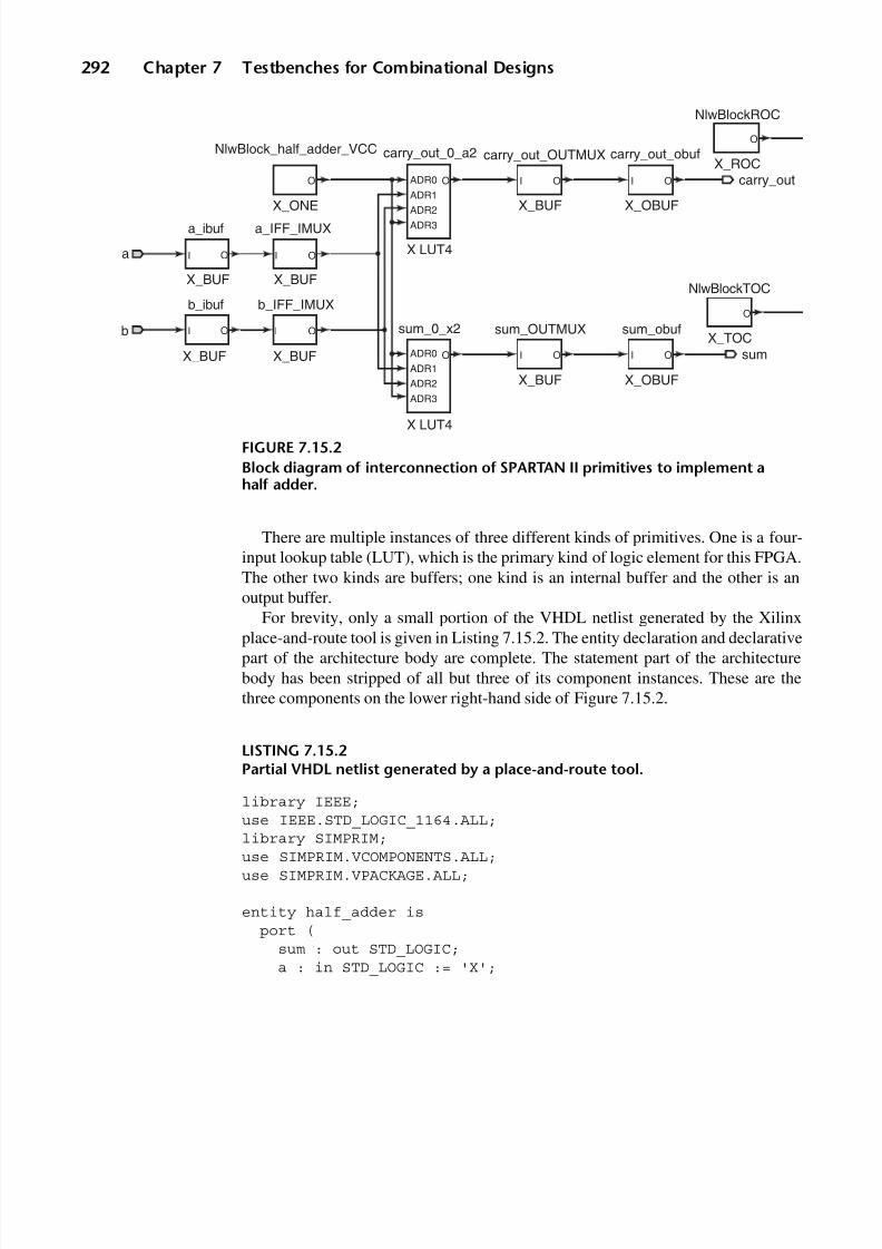
8/9/2019 VHDL for Engineers - Kenneth L. Short.pdf
http://slidepdf.com/reader/full/vhdl-for-engineers-kenneth-l-shortpdf 325/719
292 Chapter 7 Testbenches for Combinational Designs
There are multiple instances of three different kinds of primitives. One is a four-input lookup table (LUT), which is the primary kind of logic element for this FPGA.The other two kinds are buffers; one kind is an internal buffer and the other is anoutput buffer.
For brevity, only a small portion of the VHDL netlist generated by the Xilinx
place-and-route tool is given in Listing 7.15.2. The entity declaration and declarativepart of the architecture body are complete. The statement part of the architecturebody has been stripped of all but three of its component instances. These are thethree components on the lower right-hand side of Figure 7.15.2.
LISTING 7.15.2Partial VHDL netlist generated by a place-and-route tool.
library IEEE;use IEEE.STD_LOGIC_1164.ALL;
library SIMPRIM;use SIMPRIM.VCOMPONENTS.ALL;use SIMPRIM.VPACKAGE.ALL;
entity half_adder is port ( sum : out STD_LOGIC;
a : in STD_LOGIC := 'X';
FIGURE 7.15.2
Block diagram of interconnection of SPARTAN II primitives to implement ahalf adder.
NlwBlock_half_adder_VCC
NlwBlockTOC
X_TOC
NlwBlockROC
X_ROC
X_OBUFX_BUFX_ONE
X LUT4
X LUT4
ADR0
ADR1
ADR2ADR3
ADR0
ADR1
ADR2
ADR3
X_BUFX_BUF
X_BUF X_BUF
X_OBUFX_BUF
a_ibuf
b
a
b_ibuf
a_IFF_IMUX
b_IFF_IMUX
carry_out_0_a2 carry_out_OUTMUX
sum_obufsum_OUTMUXsum_0_x2
sum
carry_out_obuf
carry_outO O
O
O
O
OI
OI
OI
O
O
O I
I
I
OI
OI

8/9/2019 VHDL for Engineers - Kenneth L. Short.pdf
http://slidepdf.com/reader/full/vhdl-for-engineers-kenneth-l-shortpdf 326/719
Section 7.15 Timing Models Using VITAL and SDF 293
b : in STD_LOGIC := 'X';carry_out : out STD_LOGIC
);end half_adder;
architecture Structure of half_adder is signal a_c_0 : STD_LOGIC;signal b_c_0 : STD_LOGIC;signal carry_out_OUTMUX_0 : STD_LOGIC;signal sum_OUTMUX_1 : STD_LOGIC;signal a_c : STD_LOGIC;signal b_c : STD_LOGIC;signal sum_c : STD_LOGIC;signal carry_out_c : STD_LOGIC;signal VCC : STD_LOGIC;
begin-- several component instances have been removed
sum_0_x2 : X_LUT4 generic map(INIT => X"5A5A", LOC => "CLB_R4C1.S0" ) port map (ADR0 => b_c_0, ADR1 => VCC, ADR2 => a_c_0, ADR3 => VCC, O => sum_c);
sum_OUTMUX : X_BUF generic map(LOC => "PAD85") port map (I => sum_c, O => sum_OUTMUX_1 );
sum_obuf : X_OBUF generic map(LOC => "PAD85")
port map (I => sum_OUTMUX_1, O => sum );
end Structure;
The components instantiated in the architecture are declared in package VCOMPO-NENTS in the library SIMPRIM provided by Xilinx.
The component instantiations’ generic maps in this netlist assign values to genericsrelated to the placement of each instance on the FPGA. These are not timing generics.The timing generics are declared in the models of the instantiated components.
The first instantiation shown is the instance sum_0_x2 of the X_LUT4 primitivecomponent. This is the four-input LUT that computes the half-adder’s sum.
The second instantiation shown is the instance sum_OUTMUX of the X_BUFprimitive component. This represents multiplexing in the output block that routes thesum to the output buffer that drives the output pin.
The third instantiation is the instance sum_obuf of an output buffer primitiveX_OBUF. This buffer drives the output pin.
Each of these primitives has a VITAL compliant model in the library SIMPRIM.The VITAL model of the X_OBUF is given in Listing 7.15.3.

8/9/2019 VHDL for Engineers - Kenneth L. Short.pdf
http://slidepdf.com/reader/full/vhdl-for-engineers-kenneth-l-shortpdf 327/719
294 Chapter 7 Testbenches for Combinational Designs
LISTING 7.15.3VITAL model of X_OBUF primitive component.
library IEEE;use IEEE.std_logic_1164.all;
library IEEE;use IEEE.Vital_Primitives.all;use IEEE.Vital_Timing.all;
library simprim;use simprim.Vcomponents.all;use simprim.VPACKAGE.all;
entity X_OBUF is
generic(
Xon : boolean := true;MsgOn : boolean := true;LOC : string := "UNPLACED";
tipd_I : VitalDelayType01 := (0.000 ns, 0.000 ns);tpd_GTS_O : VitalDelayType01z := (0.000 ns, 0.000 ns, 0.000 ns, 0.000 ns,
0.000 ns, 0.000 ns);tpd_I_O : VitalDelayType01 := (0.000 ns, 0.000 ns);
PATHPULSE : time := 0 ps);
port(O : out std_ulogic;I : in std_ulogic);
attribute VITAL_LEVEL0 of
X_OBUF : entity is true;end X_OBUF;
architecture X_OBUF_V of X_OBUF is
-- attribute VITAL_LEVEL1 of
attribute VITAL_LEVEL0 ofX_OBUF_V : architecture is true;
signal GTS_resolved : std_ulogic := 'X';signal I_ipd : std_ulogic := 'X';
begin
GTS_resolved <= TO_X01(GTS);

8/9/2019 VHDL for Engineers - Kenneth L. Short.pdf
http://slidepdf.com/reader/full/vhdl-for-engineers-kenneth-l-shortpdf 328/719
Section 7.15 Timing Models Using VITAL and SDF 295
WireDelay : block
begin
VitalWireDelay (I_ipd, I, tipd_I);end block;
VITALBehavior : process (GTS_resolved, I_ipd)variable O_zd : std_ulogic;variable O_GlitchData : VitalGlitchDataType;variable I_GlitchData : SimprimGlitchDataType;variable O_prev : std_ulogic;variable InputGlitch : boolean := false;variable I_ipd_reg : std_ulogic;variable FIRST_TRANSITION_AFTER_GTS_ACTIVE : boolean := false;
begin
I_ipd_reg := TO_X01(I_ipd);if (falling_edge(GTS_resolved)) then
FIRST_TRANSITION_AFTER_GTS_ACTIVE := true;end if;
if (GTS_resolved = '0') then
if (FIRST_TRANSITION_AFTER_GTS_ACTIVE = true) then
FIRST_TRANSITION_AFTER_GTS_ACTIVE := false;else
if ((tpd_I_O(tr01) < PATHPULSE) or (tpd_I_O(tr10) < PATHPULSE)) then
else
SimprimGlitch(GlitchOccured => InputGlitch,
OutSignal => O,GlitchData => I_GlitchData,InSignalName => "I",NewValue => I_ipd_reg,PrevValue => O_Prev,PathpulseTime => PATHPULSE,MsgOn => false,MsgSeverity => warning);
end if;end if;
end if;if (InputGlitch = false) then
O_prev := TO_X01(O_zd);end if;
O_zd := VitalBUFIF0 (data => I_ipd, enable => GTS_resolved);
(Cont.)

8/9/2019 VHDL for Engineers - Kenneth L. Short.pdf
http://slidepdf.com/reader/full/vhdl-for-engineers-kenneth-l-shortpdf 329/719
296 Chapter 7 Testbenches for Combinational Designs
LISTING 7.15.3 (Cont.)
VitalPathDelay01Z (OutSignal => O,GlitchData => O_GlitchData,OutSignalName => "O",OutTemp => O_zd,Paths => (0 => (GTS_resolved'last_event, tpd_GTS_O, true),
1 => (I_ipd'last_event, VitalExtendToFillDelay(tpd_I_O), (GTS_resolved = '0'))),
Mode => VitalTransport,Xon => Xon,MsgOn => MsgOn,MsgSeverity => warning,OutputMap => "UX01ZWLH-");
if (InputGlitch = true) then
InputGlitch := false;end if;
end process;end X_OBUF_V
As is clear from Listing 7.15.3, the VITAL model for even a simple primitivecomponent can be complex. In general, the architecture for a VITAL model isseparated into four sections: wire delay, timing violation, function description, andpath delay. Not all models contain all four sections. A combinational model, such asthe half adder, does not require a timing section.
Listing 7.15.3 is provided just to give an overview of how generics are used to
provide timing information in a VITAL model. In the entity declaration three timinggenerics are declared: tipd_I, tpd_GTS_O, and tpd_I_O. For all of these genericsthe default values given in the model are 0 ns.
VITAL timing generic names follow a defined naming convention. Each namestarts with a standard prefix that defines what kind of timing parameter it is. Thereare approximately 17 different prefixes defined by the standard. Prefix tipd
indicates an interconnect delay, and prefix tpd indicates a pin-to-pin delay within acomponent.
The prefix is followed by the name(s) of the signals to which the delay applies. InListing 7.15.3 generic tipd_I is the interconnect delay modeled as a delay at inputport I. Generic tpd_I_O is pin-to-pin delay from the input of the buffer I to itsoutput O. The types of these delays are VitalDelayType01, which is an array of elements of type time. The first elements in the delay time for an output transitionfrom 0 to 1. The second element is the delay time for an output transition from 1 to 0.
The timing generic tpd_GTS_O is related to a global control signal (GTS) thatputs all output pins in their high impedance state. GTS is a pin on the FPGA thatcan be asserted during board-level testing. It is of no further interest in thisexample.

8/9/2019 VHDL for Engineers - Kenneth L. Short.pdf
http://slidepdf.com/reader/full/vhdl-for-engineers-kenneth-l-shortpdf 330/719
Section 7.15 Timing Models Using VITAL and SDF 297
SDF Standard Delay Format (SDF) was originally developed by Cadence DesignSystems as a file format for conveying timing and delay information between EDAtools for simulation of designs written in the Verilog language. It is now an IEEEstandard titled IEEE Std 1497 IEEE Standard for Standard Delay Format (SDF) for
the Electronic Process. The data in the ASCII file is represented in a tool and
language independent way and includes path delays, timing constraint values, andinterconnect delays. SDF is now used to convey timing and delay information intoboth VHDL and Verilog simulations. SDF contains constructs for the description of computed timing data for back annotation and the specification of timing constraintsfor forward annotation.
An individual component in a technology library is called a cell. For eachcomponent instance in the VHDL structural netlist the SDF file contains cell data.Each cell contains information specifying the type of cell, the instance name in thenetlist, and timing values to be back annotated to the design.
A partial listing of the SDF file for the half adder is given in Listing 7.15.4.
LISTING 7.15.4Partial SDF file for half-adder simulation.
(DELAYFILE (SDFVERSION "3.0") (DESIGN "half_adder") (DATE "Tue May 29 15:43:27 2007") (VENDOR "Xilinx") (PROGRAM "Xilinx SDF Writer") (VERSION "I.24") (DIVIDER /)
(VOLTAGE 2.375) (TEMPERATURE 85) (TIMESCALE 1 ps))(CELL(CELLTYPE "X_LUT4") (INSTANCE sum_0_x2) (DELAY (ABSOLUTE (PORT ADR0 (568)) (PORT ADR2 (1022)) (IOPATH ADR0 O (284)) (IOPATH ADR1 O (284))
(IOPATH ADR2 O (284)) (IOPATH ADR3 O (284)) )
(CELL(CELLTYPE "X_BUF") (INSTANCE carry_out_OUTMUX) (DELAY
(Cont.)
8/9/2019 VHDL for Engineers - Kenneth L. Short.pdf
http://slidepdf.com/reader/full/vhdl-for-engineers-kenneth-l-shortpdf 331/719
298 Chapter 7 Testbenches for Combinational Designs
LISTING 7.15.4 (Cont.)
(DELAY (ABSOLUTE (IOPATH I O (2603))
(CELL (CELLTYPE "X_OBUF") (INSTANCE sum_obuf) (DELAY (ABSOLUTE (PORT I (1042)) (IOPATH I O (3428))
The file starts with a header that provides information about the design and thetarget FPGA to which the file applies. The header is followed by a list of cells thatprovide values for the generics. Each cell applies to a component instance in the
netlist. Only the three cells that apply to the component instances we have previouslydiscussed are shown in the listing. The others have been removed.
The last cell is for the instance sum_obuf of the primitive X_OBUF. The SDFkeyword ABSOLUTE precedes the delay values that are to replace the default valuesduring back annotation. The keyword PORT followed by the port name I gives thevalue for generic tipd_I. The header indicates that the TIMESCALE ispicoseconds (ps). Therefore, this delay is 1042 ps or 1.042 ns. Keyword IOPATHspecifies an input to output propagation delay. In this case the delay is from I to O of the instance sum_obuf (IOPATH I O). Therefore, this delay value of 3.428 ns is forgeneric tpd_I_O.
For each SDF keyword there is a corresponding VITAL prefix (for example,IOPATH and tpd).
When the simulation is performed, the VITAL-compliant VHDL simulator readsthe SDF back-annotation file and matches the timing information to the generics inthe VHDL netlist to peform a timing-accurate simulation.
Running a VITALSimulation
To run a VITAL simulation, the VITAL library must have been previouslycompiled into a simulator library. The VHDL timing model is then compiled. Whenyou have more than one model of the UUT design entity, you must make sure thatthe desired one is used in the simulation. At this point, you would have both afunctional model and a timing model of the UUT. There are several approaches tomake sure that you simulate the desired model. One is to take advantage of defaultbinding. If the timing model is the last of the two models compiled, it will be the oneused by default. Another approach is to use a configuration declaration. Configu-ration declarations are discussed in Chapter 15.
Next the testbench is compiled. Finally, the SDF file must be specified. Thismight be done in the command line that invokes the simulator or, in a simulator withan IDE, a menu is used to specify which SDF file is to be used. Once this is done, the

8/9/2019 VHDL for Engineers - Kenneth L. Short.pdf
http://slidepdf.com/reader/full/vhdl-for-engineers-kenneth-l-shortpdf 332/719
Problems 299
simulation can be performed. The remainder of the simulation process is the same asfor a functional simulation. However, the resultant simulation waveforms show theactual delays.
Waveforms from the timing simulation of the half adder implemented in a Xilinx
XC2S15 SPARTAN II FPGA with a nominal 6 ns delay (6 ns speed grade) are shown inFigure 7.15.3. The actual input to output delay as read from the waveforms is about8.157 ns. Also, notice the glitch in the sum output when a is changed from 0 to 1 simul-taneously with b being changed from 1 to 0. This glitch does not appear in the functionalsimulation, as it is a result of primitive component propagation delays in the target PLD.
Writing VITAL timing models is a specialized area of VHDL coding and is notone of the objectives of this text. We simply use the model’s created by the PLDvendor’s place-and-route tool in our timing simulations.
PROBLE MS
7.1 What are the two basic things that need to be verified about a design?
7.2 What are the three primary constituents of a testbench and what is the purpose of each? Whatfourth constituent must be added to make a testbench self-checking?
7.3 Which constituent of a testbench is changed depending on the kind of verification beingperformed and what is it changed to for each kind of verification?
7.4 What is exhaustive verification and why is it significantly more difficult to achieve for asequential design than for a combinational design?
7.5 Why would it be preferable to have the testbench for a design written by someone other than
the person who wrote the design description?
7.6 Given a UUT with std_logic inputs, which of the nine std_logic values are used by a testbenchto form stimulus combinations?
7.7 A combinational design has n inputs. As a function of n, how many different inputcombinations must be applied by a testbench to achieve exhaustive verification? In which ordermust these input combinations be applied? What would be the number of input combinationsto be applied for the following values of n: 4, 9, 14, and 32?
FIGURE 7.15.3
Waveforms from timing simulation of half adder implemented in a SPARTAN IIFPGA.

8/9/2019 VHDL for Engineers - Kenneth L. Short.pdf
http://slidepdf.com/reader/full/vhdl-for-engineers-kenneth-l-shortpdf 333/719
300 Chapter 7 Testbenches for Combinational Designs
7.8 Modify the statements in the testbench in Listing 7.3.1 to provide stimulus for the exhaustiveverification of a UUT named three_inputs that has three inputs a, b, and c.
7.9 Write a testbench for the simulation described in Figure 6.9.3. Use a single concurrent signalassignment statement to provide the required stimulus.
7.10 For the following signal assignment statement:
c_tb <= '0', '1' after 10 ns, '0' after 25 ns, '1' after 45 ns;
assuming the simulation time is 150 ns when this statement is executed, at what time will eachnew signal value become effective?
7.11 Write a set of concurrent signal assignment statements that could be used in a testbench togenerate a stimulus for UUTs with up to six inputs. The stimulus starts from all 0s andincrements in binary. Use constants n and delay to specify the number of inputs and the delaybetween application of each new input, respectively. For a particular use, the values of n anddelay would be appropriately specified and all assignment statements beyond the nthstatement would be commented out.
7.12 Modify the testbench in Listing 7.5.1 to be a testbench for the comparator in Listing 3.2.1.Make the time between application of each stimulus value 15 ns.
7.13 In terms of the application of each stimulus value in a testbench, what is the purpose of a waitstatement? In terms of checking the actual output value against the expected output value, whatis the purpose of an assertion statement?
7.14 Write an architecture that uses a process containing a wait statement so that the architecture isexactly equivalent to that in Listing 2.6.1. Discuss why you chose the form of wait statementused and any restrictions that must be placed on the wait statement’s location.
7.15 Write a process that replaces the two concurrent signal assignment statements that generatea_tb and b_tb in the testbench architecture in Listing 7.3.1. The architecture must use only
sequential signal assignment statements without after clauses and wait statements.7.16 What is the difference between an assertion statement and a report statement?
7.17 If an assertion statement has a report clause and a severity clause together, all three clausescomprise one statement and there must be only one semicolon used and it must follow theseverity clause. What is the effect in a testbench if a semicolon is inadvertently placed after theassert clause in addition to after the severity clause?
7.18 Rewrite the assertion statements in Listing 7.5.1 so that the conditions are written in terms of incorrect behavior. In general, how might the approach of writing conditions in terms of theincorrect behavior lead to a situation where the assertions don’t indicate an error when thecircuit is actually incorrect?
7.19 Assume that a behavioral style design description named combfcn has been written for thefunction defined by the table that follows. Write a single process testbench namedcombfcn_tb that uses a loop to apply all possible input combinations to the UUT andverifies the outputs. If the UUT fails for a particular stimulus value, an integer number must bedisplayed that represents the decimal equivalent of the binary stimulus. The expected UUToutputs used in the verification must be determined by a table lookup. Allow 20 ns between theapplication of each stimulus vector.

8/9/2019 VHDL for Engineers - Kenneth L. Short.pdf
http://slidepdf.com/reader/full/vhdl-for-engineers-kenneth-l-shortpdf 334/719
Problems 301
7.20 Write a table lookup testbench for the fuel encoder described in Problem 4.12.
7.21 Write a table lookup testbench to exhaustively verify the binary-to-bargraph converter inProblem 4.27.
A demultiplexer has the following entity declaration:
entity demux_1to4 is port ( data_in: in std_logic; sel: in std_logic_vector (1 downto 0); demuxout: out std_logic_vector (3 downto 0) );end demux_1to4;
The input sel specifies, in binary, the index of the output at which a value equalto data_in appears. All other outputs are 0s.
Write a testbench that uses a constant array of records and a table lookup togenerate the stimulus and expected outputs for the testbench. Assume the record isdefined as:
type test_vector is record data_in : std_logic; sel : std_logic_vector(1 downto 0); demuxout : std_logic_vector(3 downto 0);end record;
7.22 Write a testbench that provides exhaustive verification of the ones_count design entity inProblem 4.19. The testbench must use a loop to generate all possible input combinations anduse another loop to compute the expected outputs.
7.23 Write a testbench that computes all of the valid inputs to the therm2bin design entity inProblem 4.26 and verifies the output for all valid inputs.
a b c w y
0 0 0 1 0
0 0 1 0 1
0 1 0 0 1
0 1 1 1 0
1 0 0 1 1
1 0 1 0 0
1 1 0 0 1
1 1 1 1 0

8/9/2019 VHDL for Engineers - Kenneth L. Short.pdf
http://slidepdf.com/reader/full/vhdl-for-engineers-kenneth-l-shortpdf 335/719
302 Chapter 7 Testbenches for Combinational Designs
7.24 Write a testbench that provides exhaustive verification of the 9-bit parity generator/checker inProblem 5.27. The testbench must use a loop to generate all possible input combinations anduse equations to compute the expected outputs.
7.25 Write a testbench that provides exhaustive verification of the tally scoring system inProblem 5.24. The testbench must use a loop to generate all possible input combinations and
use equations to compute the expected outputs.7.26 Two different testbenches are to be written for the BCD-to-bargraph decoder bcd_2_bar in
Problem 4.27. Each uses one of the design descriptions for the decoder that has don’t careoutputs. The approaches used in the two testbenches to compute the expected result are tablelookup and computed.
Name the two testbenches based on the technique used: table and computed. The stimulusvalues applied to the UUT by the testbench must be generated by one or more loops. Eachtestbench must provide an exhaustive verification of the decoder’s functionality, except that theoutputs for address input values of 1010 to 1111 are generated but not verified against anypredefined values. Each testbench must use assertion statements so that any failures of theUUT are reported to the console along with the input combination causing the failure.
7.27 Write a testbench to exhaustively verify the binary-to-bargraph converter in Problem 4.27 bycomputing its expected outputs using a “shift” operation.
7.28 Write a testbench that provides an exhaustive functional verification of the BCD to seven-segment decoder in Listing 4.8.2. This testbench must use two loops. The first loop generatesall valid input combinations and uses a table lookup to verify the output. The second loopgenerates all invalid inputs and verfies that these outputs are all don’t cares. How must thistestbench be modified for post-synthesis and timing simulations?
7.29 A design description and a testbench for a 4-to-1 multiplexer must be written. The entitydeclaration for the multiplexer is:
entity mux_4_to_1 is port( i : in std_logic_vector(3 downto 0); -- input data s : in std_logic_vector(1 downto 0); -- input channel selection y : out std_logic -- output data );end mux_4_to_1;
(a) Write a dataflow architecture formux_4_to_1 that consists of a single conditional signalassignment statement.
(b) Write a self-checking testbench that provides a comprehensive and functionallymeaningful verification of the design entity and is not simply an exhaustive verification.
The testbench must first make one data input a 0 (and all other data inputs 1s) and verifythe output for all possible values of the selection input. This verification must be repeatedwith the single 0 applied to each data input.
The testbench must then make one data input a 1 (and all other data inputs 0s) and check theoutput for all possible values of the selection input. This verification must be repeated with thesingle 1 applied to each data input.

8/9/2019 VHDL for Engineers - Kenneth L. Short.pdf
http://slidepdf.com/reader/full/vhdl-for-engineers-kenneth-l-shortpdf 336/719
Problems 303
7.30 Assume that you have written a design description of a combinational circuit that has thefollowing entity declaration:
entity synthfcn isport (inputs : in std_logic_vector (2 downto 0); outputs : out std_logic_vector (2 downto 0));end entity;
You have also been given a nonsynthesizable VHDL model for the system that is known to becorrect. It has the following entity declaration:
entity golden isport (goldnin : in std_logic_vector (2 downto 0); goldnout : out std_logic_vector (2 downto 0));end entity;
Write a test bench that exhaustively verifies synthfcn. If the verification fails the testbench
should display an indication for which input stimulus values it fails.7.31 Write a testbench to exhaustively verify the binary-to-bargraph converter in Problem 4.27 by
comparing its outputs with those of a behavioral intent model. The behavioral intent modelneed not be synthesizable.

8/9/2019 VHDL for Engineers - Kenneth L. Short.pdf
http://slidepdf.com/reader/full/vhdl-for-engineers-kenneth-l-shortpdf 337/719
304
Chapter 8
Latches and Flip-Flops
Previous chapters focused on combinational systems. However, most digital systemsare sequential. A sequential system’s outputs are a function of both its present inputvalue and past history of its input values. Memory elements are required in a sequentialsystem to store information that characterizes the system’s past history of input values.
In this chapter, basic latch and flip-flop memory elements are discussed. UsingVHDL, a memory element can be described either explicitly or implicitly. An explicitdescription corresponds to the instantiation of a memory element component. Incontrast, an implicit description uses a programming style that describes behaviorcorresponding to that of a memory element. In this later case, a synthesizer infers thata memory element is needed to achieve the described behavior. This chapter focuses ondescriptions that infer either latch or flip-flop memory elements.
There are several important practical considerations when describing memoryelements. One consideration is whether a particular memory element can actually besynthesized for the target PLD. This depends on the characteristics of the primitivememory elements available in the PLD. Another consideration is that the timingparameters of a PLD memory element are critical to its proper operation. Thesepractical issues are also discussed.
8 . 1 SE QU E N TI AL S YST E MSAN D THE IR ME MORY E LE ME N TS
Digital systems can be classified as either combinational or sequential. As we haveseen, a combinational system’s outputs are completely determined by its presentinput values.
8/9/2019 VHDL for Engineers - Kenneth L. Short.pdf
http://slidepdf.com/reader/full/vhdl-for-engineers-kenneth-l-shortpdf 338/719
Section 8.1 Sequential Systems and Their Memory Elements 305
State of aSequential System
In contrast, a sequential system’s outputs depend not only on its present input values,but also on its past history of input values. This history is represented by the binary present state value stored in memory elements in the sequential system. Accord-ingly, the output of a sequential system is a function of both its present input valuesand present state.
This chapter focuses on memory elements and their VHDL descriptions. Howthese memory elements are used to create more complex sequential systems isdiscussed in Chapters 9, 10, and 11.
Memory Element A single memory element is, by itself, a simple sequential system that stores 1 bit of information. A memory element has two stable states, corresponding to its storingeither a 0 or a 1. When a memory element stores a 0, it is said to be clear . When itstores a 1, it is said to be set . A memory element’s output indicates its present state.
Synchronous Inputsto a MemoryElement
A memory element has inputs that allow it to be placed into either of its two states.Synchronous inputs are inputs whose values can change the memory element’s stateonly in response to a clock pulse at its clock input.
After a memory element has been placed in a particular state, a change in thevalues of its synchronous inputs cannot change its state until the next clock pulseoccurs. In other words, the memory element stores (remembers) its state value untilthe next clock pulse.
Pulse A pulse is a short duration change in a signal’s value. For example, the signal inFigure 8.1.1(a) is normally logic 0. It transitions (changes) to 1 for a short time andthen returns to 0. Such a pulse is called a positive pulse. The duration of the pulse isits pulse width. In Figure 8.1.1(b) the signal is normally logic 1. It transitions to 0 fora short time and then returns to 1. Such a pulse is called a negative pulse.
FIGURE 8.1.1
A signal pulse: (a) positive pulse, (b) negative pulse.
1
0
1
0
trailing edge
trailing edge
leading edge
leading edge
(a)
(b)

8/9/2019 VHDL for Engineers - Kenneth L. Short.pdf
http://slidepdf.com/reader/full/vhdl-for-engineers-kenneth-l-shortpdf 339/719
306 Chapter 8 Latches and Flip-Flops
A signal transition is also called an edge. A transition from 0 to 1 is a rising edge
or positive edge. A transition from 1 to 0 is a falling edge or negative edge. The firstedge of a pulse to occur in time is its leading edge and the last edge to occur is itstrailing edge. For a positive pulse, the leading edge is a 0 to 1 transition and thetrailing edge is a 1 to 0 transition.
Clock Signal A clock signal is a train (sequence) of pulses used as a timing signal. In a fullysynchronous sequential system, a single clock signal controls when all the memoryelements can change state. Therefore, all the memory elements that change state doso at the same time. Since a synchronous system can advance from one state to thenext only in response to a clock pulse, the clock imposes a synchronous timingbehavior on the system.
Periodic andNonperiodicSignals
Examples of periodic and nonperiodic signals are shown in Figure 8.1.2. A typicalclock signal is periodic. The time between corresponding edges of a periodic signalis constant (Figure 8.1.2(a)). Therefore, changes of state occur at regular intervals.This time interval is the clock’s period (T), which is measured in seconds. Eachperiod of a clock is also referred to as a clock cycle.
The reciprocal of the clock’s period (1/T ) is its frequency, which is measured inhertz (Hz). The amount of time a periodic signal is 1 during its period ( t H ) is alsoconstant. This time is the clock’s width. The ratio of the clock’s width to its period(t H / T ), expressed as a percent, is its duty cycle.
The time between corresponding edges of a nonperiodic clock signal is notconstant (Figure 8.1.2(b)). A nonperiodic signal’s clock width may also vary.
IEEE Std 1076.6Compliant ClockSignals
IEEE Std 1076.6 limits the types allowed for a clock signal to bit, std_ulogic, andtheir subtypes (including std_logic) that have a minimum subset of values consistingof '0' and '1'. Only the values '0' and '1' from these types are allowed inexpressions representing clock levels or clock edges.
FIGURE 8.1.2
Clock signal characteristics: (a) periodic clock, (b) nonperiodic clock.
1
0
1
0
(a)
(b)
T
tH

8/9/2019 VHDL for Engineers - Kenneth L. Short.pdf
http://slidepdf.com/reader/full/vhdl-for-engineers-kenneth-l-shortpdf 340/719
Section 8.1 Sequential Systems and Their Memory Elements 307
Latch versusFlip-flop
Latches and flip-flops are the basic kinds of memory elements. A memory element iscategorized as either a latch or a flip-flop, based on to which characteristic of itsclock signal it is sensitive. The primary difference between the two is that a latch’sstate can be changed by its synchronous inputs during the entire time its clock isasserted. In contrast, a flip-flop’s state can be changed by its synchronous inputs
only at the edge of a clock pulse. Flip-flops are used much more extensively asmemory elements in PLD-based designs than are latches.
Clocked (Gated)Latch
A clocked (gated) latch is sensitive to its clock’s level. Accordingly, it displays alevel-sensitive synchronous behavior. That is, the state of the latch can be changed bythe values of its synchronous inputs during the entire time the clock is at its assertedlevel. The state of the latch at the time its clock changes to its unasserted level isstored in the latch.
If a latch is sensitive to a high or positive clock level, its clock signal is consideredasserted when it is 1. If a latch is sensitive to the low or negative clock level, its clock
signal is considered asserted when it is 0.The function table for a positive-level D latch is given in Table 8.1.1. The first two
columns are the values of the latch’s D and CLK inputs. The third column (Qt+1) isthe value of the latch’s Q output in response to the input values. The value Qt is thepreviously stored value of Q. That is, the value of Q when CLK was previouslychanged to its unasserted level.
When a latch’s clock is at its unasserted logic level, its synchronous inputs haveno effect on its state.
Flip-flop A flip-flop is a memory element whose output can change only at the time of its
clock’s transition (edge). Accordingly, it has a transition-sensitive synchronousbehavior. If a flip-flop is sensitive to a 0-to-1 transition of its clock (rising edge), theflip-flop is said to be positive edge triggered . If a flip-flop is sensitive to a 1-to-0transition of its clock (falling edge), the flip-flop is said to be negative edge triggered .
The function table for a positive-edge-triggered D flip-flop is given in Table 8.1.2.An up arrow symbol ↑ in the table indicates a positive-edge transition of a signal. Thethird column (Qt+1) is the value of the flip-flop’s Q output in response to the inputvalues D and CLK. The value Qt is the value of Q prior to the positive edge of the clock.
Table 8.1.1Function table for a
positive-level D latch.
D CLK Q t+1
0 0 Qt
0 1 0
1 0 Qt
1 1 1
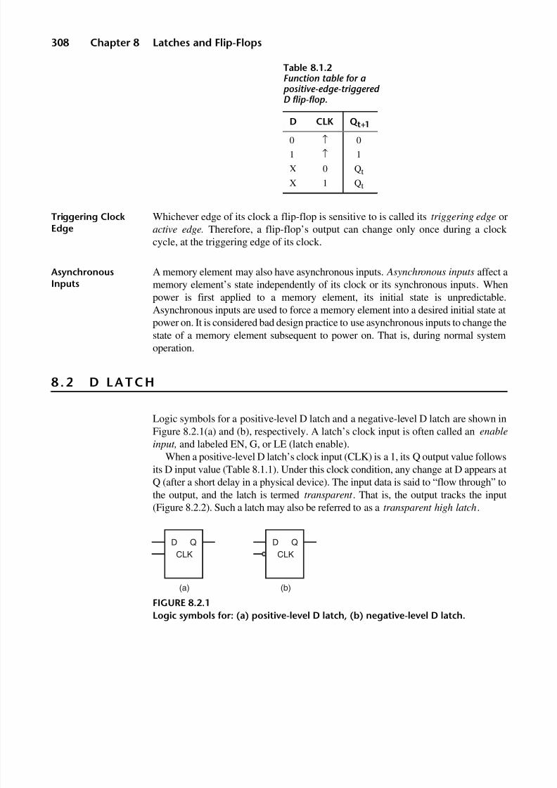
8/9/2019 VHDL for Engineers - Kenneth L. Short.pdf
http://slidepdf.com/reader/full/vhdl-for-engineers-kenneth-l-shortpdf 341/719
308 Chapter 8 Latches and Flip-Flops
Triggering ClockEdge
Whichever edge of its clock a flip-flop is sensitive to is called its triggering edge oractive edge. Therefore, a flip-flop’s output can change only once during a clock cycle, at the triggering edge of its clock.
AsynchronousInputs
A memory element may also have asynchronous inputs. Asynchronous inputs affect amemory element’s state independently of its clock or its synchronous inputs. Whenpower is first applied to a memory element, its initial state is unpredictable.Asynchronous inputs are used to force a memory element into a desired initial state atpower on. It is considered bad design practice to use asynchronous inputs to change thestate of a memory element subsequent to power on. That is, during normal systemoperation.
8 . 2 D LA T C H
Logic symbols for a positive-level D latch and a negative-level D latch are shown inFigure 8.2.1(a) and (b), respectively. A latch’s clock input is often called an enable
input, and labeled EN, G, or LE (latch enable).When a positive-level D latch’s clock input (CLK) is a 1, its Q output value follows
its D input value (Table 8.1.1). Under this clock condition, any change at D appears atQ (after a short delay in a physical device). The input data is said to “flow through” tothe output, and the latch is termed transparent . That is, the output tracks the input(Figure 8.2.2). Such a latch may also be referred to as a transparent high latch.
Table 8.1.2Function table for apositive-edge-triggeredD flip-flop.
D CLK Q t+1
0 ↑ 0
1 ↑ 1
X 0 Qt
X 1 Qt
FIGURE 8.2.1
Logic symbols for: (a) positive-level D latch, (b) negative-level D latch.
CLK
(a)
D Q
CLK
(b)
D Q

8/9/2019 VHDL for Engineers - Kenneth L. Short.pdf
http://slidepdf.com/reader/full/vhdl-for-engineers-kenneth-l-shortpdf 342/719
Section 8.2 D Latch 309
When CLK is changed from 1 to 0, Q keeps the value it had at the time CLK waslast equal to 1. Under this clock condition, the value of D when CLK was last a 1 isstored. As long as CLK remains 0, any subsequent changes in D have no effect on Q.
Since changes in Q, corresponding to changes in D, are conditioned on the clock level, D is a synchronous input. Since the value stored in a positive-level D latch is
always equal to the value of D when CLK was last equal to 1, the D input is thoughtof as the data input. A D latch may also have a Q output, which is, by definition, thecomplement of Q.
Latch Inference We can cause a memory element to be synthesized by writing code that is recognizedas implying the need for a memory element. The technique used by a synthesizer todetermine, from its interpretation of the VHDL code, when a latch must be synthe-sized is called latch inference.
When Is a LatchInferred
In general, a latch is inferred when a statement conditionally makes an assignment toa signal or variable and the condition does not involve a clock edge. Such anassignment is called an asynchronous assignment .
For example, an if statement whose if clause contains an asynchronous assignmentto a signal, but which has no terminating else clause, causes a synthesizer to inferthat a latch is required. A latch is required because, when the condition is not true,the signal is not assigned a new value. Therefore, the signal must retain itsprevious value, necessitating a latch. When such an if statement is synthesized,the synthesizer may give a warning such as “Latch generated from process for
signal q, probably caused by a missing assignment in an if or case statement.” Thesignal (or variable) that is conditionally assigned is the output of the inferred
latch.
Latch TemplateUsing an IfStatement
An if statement template for synthesizing a latch is given in Figure 8.2.3.The clock-level condition following keyword if is written to evaluate true when the
clock is asserted. Included in the then clause are one or more assignment statements.Any signals or variables assigned values by these statements are implemented asoutputs of latches.
FIGURE 8.2.2
Waveforms representing the functional behavior of a positive-level D latch.
D
CLK
Q

8/9/2019 VHDL for Engineers - Kenneth L. Short.pdf
http://slidepdf.com/reader/full/vhdl-for-engineers-kenneth-l-shortpdf 343/719
310 Chapter 8 Latches and Flip-Flops
D Latch Description A D latch description using the template in Figure 8.2.3 is given in Listing 8.2.1. Theorder of the clock and the other inputs in the sensitivity list is not important.
However, the sensitivity list must contain all of the signals read within the process.
This architecture has a single process. Both d and clk must be included in the
process’ sensitivity list, since, if either changes value, it is possible for the output of the D latch to change value.
If there is an event on either input, the process is executed. If clk = '1', then q
gets assigned the value of d. Since there is no else clause, if clk is not '1', there isno assignment to q. This later condition implies that the old value of q must beremembered, and hence the need for a latch.
LISTING 8.2.1D latch description.
library ieee;use ieee.std_logic_1164.all;
entity d_latch is
port (d: in std_logic; -- data inputclk: in std_logic; -- clock inputq: out std_logic -- output);
end d_latch;
architecture behavioral of d_latch is
beginprocess (d, clk)
begin
if clk = '1' then
q <= d;end if;
end process;end behavioral;
[process_label:] process (<clock_signal>, <input_signals>)
<declarations>
begin
if <clock_level> then
<sequence_of_statements>
end if ;
end process [process_label];
FIGURE 8.2.3
Template for latch inference using an if statement.

8/9/2019 VHDL for Engineers - Kenneth L. Short.pdf
http://slidepdf.com/reader/full/vhdl-for-engineers-kenneth-l-shortpdf 344/719
Section 8.2 D Latch 311
Since we intended to describe a D latch, the else clause was intentionally left out sothat the synthesizer infers the need for a latch. From Listing 8.2.1 the synthesizersynthesizes the latch in Figure 8.2.4.
Equivalent D LatchDescriptions
The incomplete if statement in Listing 8.2.1 is essentially equivalent to the followingcomplete if statement
if clk = '1' then
q <= d;else
q <= q;end if;
that assigns the signal q to itself when the clock condition is not true. However, thisif statement can be used only when the mode of q is either buffer or inout. Somecompilers may treat the
q <= q;
self assignment as redundant and simply remove it.
An if statement that is exactly equivalent to the one in Listing 8.2.1 is:if clk = '1' then
q <= d;else
null;end if;
This if statement can be used with q being mode out. Recall that the null keywordmeans nothing is to be done.
All three if statements infer the same D latch. However, technically, the if statement that assigns q <= q when the clock condition is false causes all pending
transactions on the driver for q to be replaced with the transaction assigning thecurrent value of q to q, 1 δ later. In contrast, use of the null statement leaves anypending transactions for q on its driver.
Negative-LevelLatch Description
To describe a negative-level latch, the if statement’s clock-level condition is simplychanged to:
clk = '0'
FIGURE 8.2.4Latch inferred by synthesizer from description in Listing 8.2.1.
clkd
q
lat
q
DC
Q
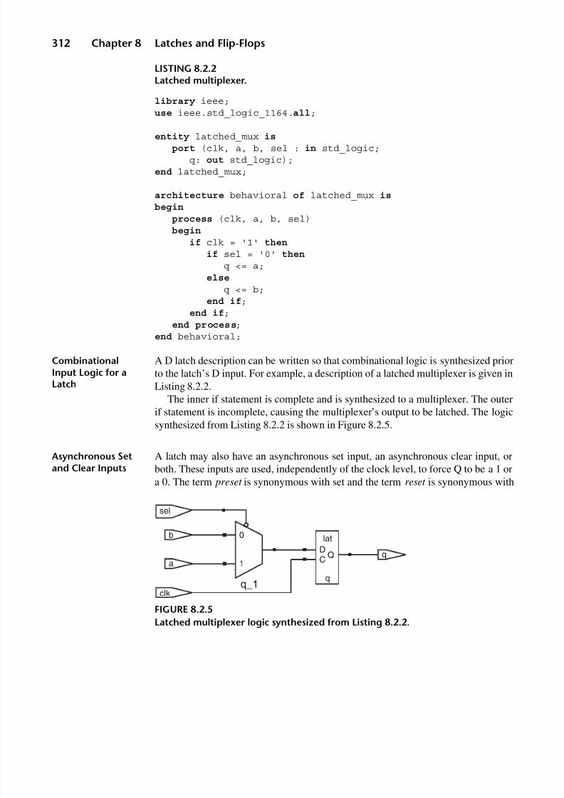
8/9/2019 VHDL for Engineers - Kenneth L. Short.pdf
http://slidepdf.com/reader/full/vhdl-for-engineers-kenneth-l-shortpdf 345/719
312 Chapter 8 Latches and Flip-Flops
LISTING 8.2.2Latched multiplexer.
library ieee;use ieee.std_logic_1164.all;
entity latched_mux isport (clk, a, b, sel : in std_logic;
q: out std_logic);end latched_mux;
architecture behavioral of latched_mux is
begin
process (clk, a, b, sel)begin
if clk = '1' then
if sel = '0' then
q <= a;else
q <= b;end if;
end if;end process;
end behavioral;
CombinationalInput Logic for aLatch
A D latch description can be written so that combinational logic is synthesized priorto the latch’s D input. For example, a description of a latched multiplexer is given inListing 8.2.2.
The inner if statement is complete and is synthesized to a multiplexer. The outerif statement is incomplete, causing the multiplexer’s output to be latched. The logicsynthesized from Listing 8.2.2 is shown in Figure 8.2.5.
Asynchronous Setand Clear Inputs
A latch may also have an asynchronous set input, an asynchronous clear input, orboth. These inputs are used, independently of the clock level, to force Q to be a 1 ora 0. The term preset is synonymous with set and the term reset is synonymous with
FIGURE 8.2.5
Latched multiplexer logic synthesized from Listing 8.2.2.
sel
b
a
0
1
q_1
q
lat
q
DC
Q
clk

8/9/2019 VHDL for Engineers - Kenneth L. Short.pdf
http://slidepdf.com/reader/full/vhdl-for-engineers-kenneth-l-shortpdf 346/719
Section 8.2 D Latch 313
clear. Any asynchronous inputs must be kept unasserted for normal synchronousoperation. We can add an asynchronous set or clear input, or both, to a D latchsymbol as symbolized in Figure 8.2.6.
The D latch description in Listing 8.2.3 includes asserted-low asynchronous setand clear inputs.
Since all of the latch’s inputs are in the process’s sensitivity list, an event onany input causes the process to execute. The if statement first checks whetherset_bar is asserted. If it is, q is assigned a '1'. If not, the first elsif clausechecks whether clear_bar is asserted. If clear_bar is asserted, then q isassigned a '0'.
LISTING 8.2.3D latch with asynchronous set and clear inputs.
library ieee;use ieee.std_logic_1164.all;
entity d_latch is
port (d, clk, set_bar, clear_bar : in std_logic;q: out std_logic);
end d_latch;
architecture behavioral of d_latch is
begin
process (d, clk, set_bar, clear_bar)begin
if set_bar = '0' then -- asynchronous set
q <= '1';elsif clear_bar = '0' then -- asynchronous clear
q <= '0';elsif clk = '1' then -- d latch
q <= d;end if;
end process;end behavioral;
FIGURE 8.2.6
D latch with asserted low-asynchronous set and clear inputs.
CLK
CLR
SET
D Q
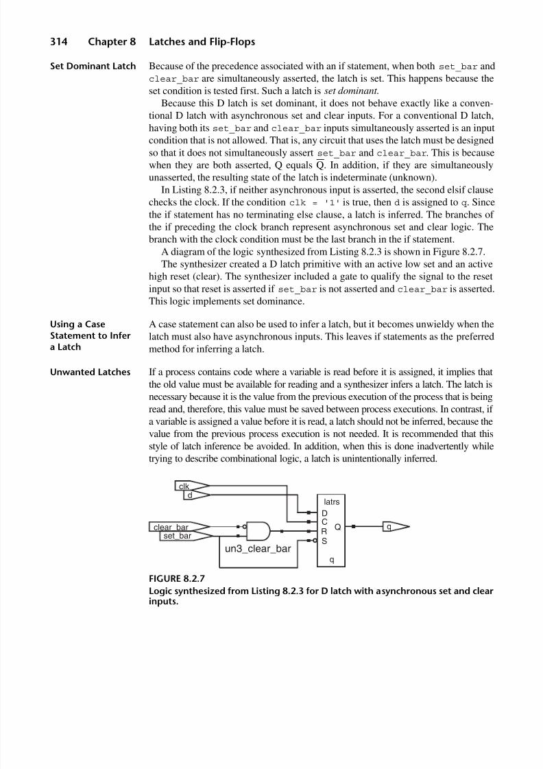
8/9/2019 VHDL for Engineers - Kenneth L. Short.pdf
http://slidepdf.com/reader/full/vhdl-for-engineers-kenneth-l-shortpdf 347/719
314 Chapter 8 Latches and Flip-Flops
Set Dominant Latch Because of the precedence associated with an if statement, when both set_bar andclear_bar are simultaneously asserted, the latch is set. This happens because theset condition is tested first. Such a latch is set dominant.
Because this D latch is set dominant, it does not behave exactly like a conven-tional D latch with asynchronous set and clear inputs. For a conventional D latch,
having both its set_bar and clear_bar inputs simultaneously asserted is an inputcondition that is not allowed. That is, any circuit that uses the latch must be designedso that it does not simultaneously assert set_bar and clear_bar. This is becausewhen they are both asserted, Q equals Q. In addition, if they are simultaneouslyunasserted, the resulting state of the latch is indeterminate (unknown).
In Listing 8.2.3, if neither asynchronous input is asserted, the second elsif clausechecks the clock. If the condition clk = '1' is true, then d is assigned to q. Sincethe if statement has no terminating else clause, a latch is inferred. The branches of the if preceding the clock branch represent asynchronous set and clear logic. Thebranch with the clock condition must be the last branch in the if statement.
A diagram of the logic synthesized from Listing 8.2.3 is shown in Figure 8.2.7.The synthesizer created a D latch primitive with an active low set and an active
high reset (clear). The synthesizer included a gate to qualify the signal to the resetinput so that reset is asserted if set_bar is not asserted and clear_bar is asserted.This logic implements set dominance.
Using a CaseStatement to Infera Latch
A case statement can also be used to infer a latch, but it becomes unwieldy when thelatch must also have asynchronous inputs. This leaves if statements as the preferredmethod for inferring a latch.
Unwanted Latches If a process contains code where a variable is read before it is assigned, it implies that
the old value must be available for reading and a synthesizer infers a latch. The latch isnecessary because it is the value from the previous execution of the process that is beingread and, therefore, this value must be saved between process executions. In contrast, if a variable is assigned a value before it is read, a latch should not be inferred, because thevalue from the previous process execution is not needed. It is recommended that thisstyle of latch inference be avoided. In addition, when this is done inadvertently whiletrying to describe combinational logic, a latch is unintentionally inferred.
FIGURE 8.2.7
Logic synthesized from Listing 8.2.3 for D latch with asynchronous set and clearinputs.
clkd
un3_clear_bar
q
latrs
q
CD
RQ
set_barclear_bar
S

8/9/2019 VHDL for Engineers - Kenneth L. Short.pdf
http://slidepdf.com/reader/full/vhdl-for-engineers-kenneth-l-shortpdf 348/719
Section 8.3 Detecting Clock Edges 315
Using a ConcurrentSignal Assignmentto Infer a Latch
A concurrent signal assignment statement can also be used to infer a latch, althoughthis is not a preferred approach. For example, the process statement in Listing 8.2.3can be replaced by the single conditional signal assignment statement
q <= '1' when set_bar = '0' else
'0' when clear_bar = '0' else
d when clk = '1';
to cause the latch in Figure 8.2.7 to be synthesized.
UnaffectedKeyword
An equivalent, but less concise, way to write the previous concurrent signalassignment is:
q <= '1' when set_bar = '0' else
'0' when clear_bar = '0' else
d when clk = '1' else
unaffected;
This statement uses the keyword unaffected. Keyword unaffected is used inconcurrent statements to indicate an assignment that does not affect the driver of thetarget. It has the same effect that null has in sequential assignments.
8 . 3 DE TE CT IN G C L OC K E DGE S
Since a flip-flop is only sensitive to its synchronous inputs at the occurrence of a
triggering clock edge, its description requires detection of each triggering clock edge.
Positive Clock EdgeConditions
There are several boolean type expressions that can be used to describe a conditionthat corresponds to the occurrence of a clock edge. These expressions are also calledsynchronous conditions. Expressions for a positive clock-edge condition are summa-rized in Table 8.3.1.
Assuming a clock signal named clk, the first expression in Table 8.3.1 is written:
clk'event and clk = '1'
Table 8.3.1Expressions for a positive clock-edge condition.
clock_signal_name'event and clock_signal_name = '1'
not clock_signal_name'stable and clock_signal_name = '1'
rising_edge(clock_signal_name)

8/9/2019 VHDL for Engineers - Kenneth L. Short.pdf
http://slidepdf.com/reader/full/vhdl-for-engineers-kenneth-l-shortpdf 349/719
316 Chapter 8 Latches and Flip-Flops
Event Attribute This expression is the and of two subexpressions. The first is an event attribute.Recall that an event attribute is an expression that is true when there is a change inthe associated signal’s value. An event attribute for a signal S (S’event) is true only if S changes value during the current simulation cycle; see “Signal Attributes” onpage 241.
The other subexpression, clk = '1', evaluates true when clk is a '1'. Thesetwo conditions can be true simultaneously only if clk has just changed (an event) toa '1'. Assuming that during a simulation clk is assigned only the values '0' or'1', these conditions being true mean that clock had a positive-edge transitionduring the current simulation cycle.
The order of the subexpressions is of no consequence. So,
clk = '1' and clk'event
is equivalent to the previous expression.
Stable Attribute Another boolean expression for a positive edge uses the signal attribute stable.The stable attribute forms an expression that is true only when there is no changein the associated signal’s value during the current simulation cycle. Accordingly, theexpression
not clk'stable
is true when clk is not stable during a simulation cycle, which is equivalent to an eventon clk. The and of this expression with the expression clk = '1' is true when thereis a positive edge on clk.
rising_edgeFunction
The first two expressions in Table 8.3.1 are fine for synthesis, but have a drawback when simulating std_logic signals. Both expressions detect a transition to a '1' statefrom any other state. Therefore, they are true for a change from a metalogic value,such as 'U' to '1'. This could give a misleading result during a simulation.
This problem is eliminated by using the function rising_edge, defined inpackage STD_LOGIC_1164. This function is true only if clk makes a transitionfrom '0' to '1'. It is not true for a transition from any other value to a '1'.
NegativeClock-EdgeConditions
Expressions for a negative clock-edge condition are given in Table 8.3.2.
Table 8.3.2Expressions for a negative clock-edge condition.
clock_signal_name'event and clock_signal_name = '0'
not clock_signal_name'stable and clock_signal_name = '0'
falling_edge(clock_signal_name)
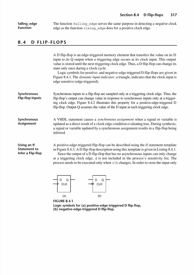
8/9/2019 VHDL for Engineers - Kenneth L. Short.pdf
http://slidepdf.com/reader/full/vhdl-for-engineers-kenneth-l-shortpdf 350/719
Section 8.4 D Flip-flops 317
falling_edgeFunction
The function falling_edge serves the same purpose in detecting a negative clock edge as the function rising_edge does for a positive clock edge.
8 . 4 D F L I P - FL O PS
A D flip-flop is an edge-triggered memory element that transfers the value on its Dinput to its Q output when a triggering edge occurs at its clock input. This outputvalue is stored until the next triggering clock edge. Thus, a D flip-flop can change itsstate only once during a clock cycle.
Logic symbols for positive- and negative-edge-triggered D flip-flops are given inFigure 8.4.1. The dynamic input indicator , a triangle, indicates that the clock input isedge sensitive (edge triggered).
SynchronousFlip-flop Inputs
Synchronous inputs to a flip-flop are sampled only at a triggering clock edge. Thus, theflip-flop’s output can change value in response to synchronous inputs only at a trigger-ing clock edge. Figure 8.4.2 illustrates this property for a positive-edge-triggered Dflip-flop. Output Q assumes the value of the D input at each triggering clock edge.
SynchronousAssignment
A VHDL statement causes a synchronous assignment when a signal or variable isupdated as a direct result of a clock edge condition evaluating true. During synthesis,a signal or variable updated by a synchronous assignment results in a flip-flop beinginferred.
Using an IfStatement toInfer a Flip-flop
A positive-edge-triggered flip-flop can be described using the if statement templatein Figure 8.4.3. A D flip-flop description using this template is given in Listing 8.4.1.
Since the output of a D flip-flop that has no asynchronous inputs can only changeat a triggering clock edge, d is not included in the process’s sensitivity list. Theprocess needs to be executed only when clk changes. In order to store the input only
FIGURE 8.4.1
Logic symbols for (a) positive-edge-triggered D flip-flop,(b) negative-edge-triggered D flip-flop.
CLK
(a)
D Q
CLK
(b)
D Q
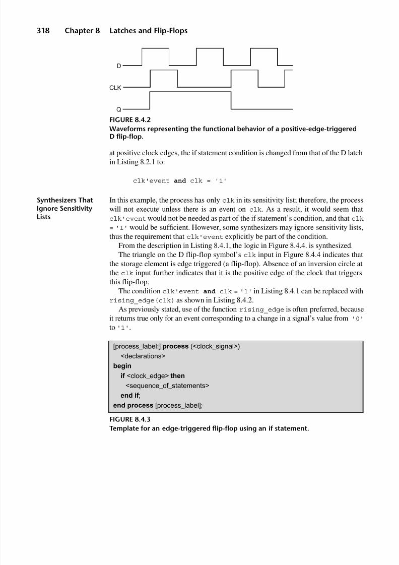
8/9/2019 VHDL for Engineers - Kenneth L. Short.pdf
http://slidepdf.com/reader/full/vhdl-for-engineers-kenneth-l-shortpdf 351/719
318 Chapter 8 Latches and Flip-Flops
at positive clock edges, the if statement condition is changed from that of the D latchin Listing 8.2.1 to:
clk'event and clk = '1'
Synthesizers ThatIgnore SensitivityLists
In this example, the process has only clk in its sensitivity list; therefore, the processwill not execute unless there is an event on clk. As a result, it would seem thatclk'event would not be needed as part of the if statement’s condition, and that clk= '1' would be sufficient. However, some synthesizers may ignore sensitivity lists,thus the requirement that clk'event explicitly be part of the condition.
From the description in Listing 8.4.1, the logic in Figure 8.4.4. is synthesized.The triangle on the D flip-flop symbol’s clk input in Figure 8.4.4 indicates that
the storage element is edge triggered (a flip-flop). Absence of an inversion circle atthe clk input further indicates that it is the positive edge of the clock that triggersthis flip-flop.
The condition clk'event and clk = '1' in Listing 8.4.1 can be replaced withrising_edge(clk) as shown in Listing 8.4.2.
As previously stated, use of the function rising_edge is often preferred, becauseit returns true only for an event corresponding to a change in a signal’s value from '0'
to '1'.
FIGURE 8.4.2
Waveforms representing the functional behavior of a positive-edge-triggeredD flip-flop.
D
CLK
Q
[process_label:] process (<clock_signal>)
<declarations>
begin
if <clock_edge> then
<sequence_of_statements>
end if ;
end process [process_label];
FIGURE 8.4.3
Template for an edge-triggered flip-flop using an if statement.

8/9/2019 VHDL for Engineers - Kenneth L. Short.pdf
http://slidepdf.com/reader/full/vhdl-for-engineers-kenneth-l-shortpdf 352/719
Section 8.4 D Flip-flops 319
LISTING 8.4.1Positive-edge-triggered D flip-flop.
library ieee;use ieee.std_logic_1164.all;
entity d_ff_pe isport (
d, clk: in std_logic;q: out std_logic;
end d_ff_pe;
architecture behavioral of d_ff_pe is
begin
process (clk)begin
if clk'event and clk = '1' then
q <= d;end if;end process;
end behavioral;
Negative edge triggering is easily accomplished by changing the if condition to
clk'event and clk = '0'
or to:
falling_edge(clk)
Using a WaitStatement to Infera Flip-flop
Edge triggering can also be accomplished using a wait statement. A template forinferring a flip-flop using a wait until statement is given in Figure 8.4.5.
When a single wait statement is used in a process to infer a flip-flop, it must beeither the first or last statement in the process.
For example, the architecture for a positive-edge-triggered D flip-flop is describedin Listing 8.4.3 using a wait until statement. The logic synthesized is the same as forthe description in Listing 8.4.1.
FIGURE 8.4.4
Logic synthesized from Listing 8.4.1 for a positive-edge-triggered D flip-flop.
dclk
q
q
D Q

8/9/2019 VHDL for Engineers - Kenneth L. Short.pdf
http://slidepdf.com/reader/full/vhdl-for-engineers-kenneth-l-shortpdf 353/719
320 Chapter 8 Latches and Flip-Flops
LISTING 8.4.2Positive-edge-triggered D flip-flop architecture using rising_edge function.
architecture behavioral2 of d_ff_pe is
begin
process (clk)
beginif rising_edge(clk) then
q <= d;end if;
end process;end behavioral2;
Clock EdgeConditions in a WaitUntil Statement
Any of the conditions in Tables 8.3.1 or 8.3.2 can be used in a wait until statementto specify a clock edge. In addition, the condition clk = '1' or clk = '0' is suffi-cient to represent a positive or negative clock edge, respectively. This is true
because the wait until statement suspends execution of the process until there is anevent on a signal in its condition and the condition evaluates true. (See “Wait Until”on page 264.)
Each signal assigned a value by an assignment statement following the waitstatement infers a separate flip-flop.
Using a VariableAssignment to Infera Flip-flop
The interpretation of whether a flip-flop should be inferred from an assignment to avariable following a wait statement is more complex. If the value of the variable isread before the variable is assigned a value, a flip-flop should be inferred.
Asynchronous Setand Clear Inputs
Asynchronous set and clear inputs can be added to D flip-flop descriptions, just asthey were added to D latch descriptions.
A signal (or variable) that is synchronously assigned may also be asynchronouslyassigned to realize asynchronous set and clear operations. A template for this isgiven in Figure 8.4.6.
[process_label:] process
<declarations>
begin
wait until <clock_edge>
<sequence_of_statements>
end process [process_label];
FIGURE 8.4.5
Template for inferring a flip-flop using a wait until statement.

8/9/2019 VHDL for Engineers - Kenneth L. Short.pdf
http://slidepdf.com/reader/full/vhdl-for-engineers-kenneth-l-shortpdf 354/719
Section 8.4 D Flip-flops 321
LISTING 8.4.3Positive-edge-triggered D flip-flop architecture using a wait until statement.
architecture behavioral of d_ff_pe_wait is
begin
process
begin wait until clk = '1';
q <= d;end process;
end behavioral;
The conditions associated with the branches prior to the last elsif branch don’tinvolve a clock edge. Assignment statements in these branches make asynchronousassignments. The last elsif condition is a clock-edge condition and assignment state-ments in this branch are synchronous assignments.
The sensitivity list must include the clock signal, all signals read in the conditions of
the asynchronous elsif branches, and all signals read in the sequential statementscontrolled by those conditions. No other signals should be included in the sensitivity list.
A D flip-flop with asynchronous set and clear is described in Listing 8.4.4.
Limitations WhenUsing WaitStatements toInfer Flip-flops
A drawback in using a wait statement to infer a flip-flop is that it is not possible toadd asynchronous set and/or clear inputs, because all assignments executed after thewait are synchronous assignments. However, synchronous set and/or clear inputs canbe described using a wait statement.
[process_label:] process (<clock_signal, asynch_signals>)
<declarations>begin
if <condition1> then
<sequence_of_statements>
elsif <condition2> then
<sequence_of_statements>
. . .
elsif <conditionn> then
<sequence_of_statements>
elsif <clock_edge> then
<sequence_of_statements>
end if ;
end process [process_label];
FIGURE 8.4.6
Template for an edge-triggered flip-flop with asynchronous set or clear.

8/9/2019 VHDL for Engineers - Kenneth L. Short.pdf
http://slidepdf.com/reader/full/vhdl-for-engineers-kenneth-l-shortpdf 355/719
322 Chapter 8 Latches and Flip-Flops
LISTING 8.4.4D flip-flop with asynchronous set and clear.
library ieee;use ieee.std_logic_1164.all;
entity d_ff_pe_asc isport (
d, clk: in std_logic;set_bar, clear_bar: in std_logic; -- asynchronous set and clear inputsq: out std_logic);
end d_ff_pe_asc;
architecture behavioral of d_ff_pe_asc is
begin
process (clk, set_bar, clear_bar)begin
if set_bar = '0' thenq <= '1';
elsif clear_bar = '0' then
q <= '0';elsif rising_edge(clk) then
q <= d;end if;
end process;end behavioral
Synchronous Setand Clear Inputs
Synchronous set and clear inputs can be used with D flip-flops in place of, or inaddition to, asynchronous set and clear inputs. A synchronous set or clear input hasan effect only at a triggering clock edge. Accordingly, synchronous set and clearinputs are not included in the process’s sensitivity list. Listing 8.4.5 is a descriptionof a D flip-flop with synchronous set and clear.
LISTING 8.4.5D flip-flop with synchronous set and clear.
library ieee;use ieee.std_logic_1164.all;
entity d_ff_pe_ssc is
port (d, clk: in std_logic;set_bar, clear_bar: in std_logic; -- synchronous set and clear inputsq: out std_logic);
end d_ff_pe_ssc;

8/9/2019 VHDL for Engineers - Kenneth L. Short.pdf
http://slidepdf.com/reader/full/vhdl-for-engineers-kenneth-l-shortpdf 356/719
Section 8.4 D Flip-flops 323
architecture behavioral of d_ff_pe_ssc is
begin
process (clk)begin
if rising_edge(clk) then
if set_bar = '0' then
q <= '1';elsif clear_bar = '0' then
q <= '0';else
q <= d;end if;
end if;end process;
end behavioral
The synthesized logic for the D flip-flop with synchronous set and clear inListing 8.4.5 is shown in Figure 8.4.7.
Using a ConcurrentSignal AssignmentStatement to Infera Flip-flop
A conditional signal assignment statement can also be used to infer a flip-flop: Forexample, the process statement in Listing 8.4.4 can be replaced by the single condi-tional signal assignment statement:
q <= '1' when set_bar = '0' else
'0' when clear_bar = '0' else
d when rising_edge(clk);
FIGURE 8.4.7
Synthesized logic for D flip-flop with synchronous set and clear.
D Q q
q
un3_clear_bar
un2_clear_bar
q_4
e
d1
0e
d
e
dd
clk
clear_barset_bar

8/9/2019 VHDL for Engineers - Kenneth L. Short.pdf
http://slidepdf.com/reader/full/vhdl-for-engineers-kenneth-l-shortpdf 357/719
324 Chapter 8 Latches and Flip-Flops
8 . 5 E N A BL ED ( GA TE D) F L I P- F LO P
All previous D flip-flop examples stored the data at their D inputs at each triggeringclock edge. Thus, data was stored for no longer than one clock cycle. Often there is
a need to have a flip-flop store its data for more than one clock cycle. This isachieved by having the flip-flop store its input data only at selected triggering clock edges and not at others. At the other triggering clock edges, we want the flip-flop toremain in its previous state. To accomplish this, we add an enable (gate) input to theflip-flop. A D flip-flop with an enable input stores its input data at a triggering clock edge only if its enable input is asserted.
Approaches toEnabling a Flip-flop
There are two common approaches to creating an enabled flip-flop: gated clock orgated data. The gated clock approach, which we discuss first, is generally to beavoided. Instead, the gated data approach is preferred.
Gated ClockApproach
An obvious, but risky, approach to creating an enabled flip-flop is to gate the clock signal using the enable signal, so that the clock signal reaches the flip-flop’s clock input only when the enable input is asserted. A description using this approach isgiven in Listing 8.5.1.
LISTING 8.5.1Gating a flip-flop’s clock—considered a poor design practice.
library ieee;use ieee.std_logic_1164.all;
entity d_ff_gated is
port (d, clk: in std_logic;en: in std_logic; -- enable inputq: out std_logic;
end d_ff_gated;
architecture behavioral of d_ff_gated is
signal gated_clk : std_logic;begin
gated_clk <= clk when en = '1' else '1';process (gated_clk)begin
if gated_clk'event and gated_clk = '1' then
q <= d;end if;
end process;end behavioral;

8/9/2019 VHDL for Engineers - Kenneth L. Short.pdf
http://slidepdf.com/reader/full/vhdl-for-engineers-kenneth-l-shortpdf 358/719
Section 8.5 Enabled (Gated) Flip-flop 325
The architecture contains two concurrent statements. The conditional signalassignment statement assigns gated_clk the value of clk when the enable input enis '1'. Otherwise, gated_clk is held at '1'. The process statement infers an edge-
triggered flip-flop with gated_clk as its clock signal. The logic synthesized fromthis description is shown in Figure 8.5.1.The synthesized logic appears to do what is required. When en is a '0', the clock
input of the flip-flop is held at '1'. When en is a '1', the clock signal passesthrough the multiplexer to the flip-flop’s clock input.
If the signal at the en input has glitches, there is a problem with this approach.Often, this signal is the output of a combinational system, which might produceglitches as its inputs change. As discussed in “Post-Synthesis and Timing Verifica-tions for Combinational Designs” on page 284, synthesizers do not create hazard-free combinational logic.
For example, a 0-1-0 glitch (a static 0 hazard) at the en input while the clock is 0
produces a 1-0-1 glitch at the flip-flop’s clock input, causing it to store the data at itsD input. Because the flip-flop can be incorrectly triggered by glitches from the clock gating circuit, using this approach is a poor design practice. Note that any glitches onen while the clock is high will not clock the flip-flop. Thus, a period of time equal tothe clock width is available for any glitches on the en input to have passed withoutadversely affecting the circuit’s operation.
There are situations in the design of low-power circuits where a clock is inten-tionally gated. In such cases, it is the designer’s responsibility to ensure that thecircuit producing the enable signal is glitch free or that the clock is high for a suffi-cient time for any glitches to have ended.
Gated DataApproach
The preferred approach to enabling a flip-flop is to gate the data to the flip-flopinstead of gating the clock. A description of a gated data flip-flop is given inListing 8.5.2.
This description consists of a single process. Signal q_sig is declared so thatoutput q can be read. The outer if statement infers a flip-flop. The inner if statementsays that the flip-flop should store d only if en = '1'. Otherwise, it should store
FIGURE 8.5.1
Hierarchical view of logic synthesized from Listing 8.5.1.
en
clk
d
0
1
gated_clk
1
q
q
D Q

8/9/2019 VHDL for Engineers - Kenneth L. Short.pdf
http://slidepdf.com/reader/full/vhdl-for-engineers-kenneth-l-shortpdf 359/719
326 Chapter 8 Latches and Flip-Flops
LISTING 8.5.2Gating a flip-flop’s data using an enable input.
library ieee;use ieee.std_logic_1164.all;
entity d_ff_enabled isport (d, clk, en: in std_logic;
q: out std_logic);end d_ff_enabled;
architecture behavioral of d_ff_enabled is
signal q_sig : std_logic;begin
process (clk)begin
if clk'event and clk = '1' then
if en = '1' thenq_sig <= d;
else
q_sig <= q_sig;end if;
end if;end process;q <= q_sig;
end behavioral;
q_sig. This latter action has been explicitly specified by the inclusion of an elseclause containing a statement assigning the current value of q_sig to q_sig.
The synthesis of Listing 8.5.2 produces the logic in Figure 8.5.2.The flip-flop’s output is fed back to one of the multiplexer’s inputs. The other
multiplexer input is d. The value of en determines whether d or q_sig (the value
FIGURE 8.5.2
Synthesized logic for a D flip-flop with an enable (gated data).
clk
en
d
q_2
q
q
D Q
0
1

8/9/2019 VHDL for Engineers - Kenneth L. Short.pdf
http://slidepdf.com/reader/full/vhdl-for-engineers-kenneth-l-shortpdf 360/719
Section 8.5 Enabled (Gated) Flip-flop 327
currently stored in the flip-flop) appears at the flip-flop primitive’s D input. Whenthe enable condition is false, the data currently stored in the flip-flop is recirculatedthrough the multiplexer at each triggering clock edge. Note that the flip-flopprimitive in Figure 8.5.2 actually stores the value at its D input at every triggeringclock edge.
Glitches on the en input do not affect the state of the flip-flop, as long as en is
stable for a time equal to the flip-flop’s setup time prior to the positive edge of theclock. If the enable signal is derived from logic clocked by the same clock, anychanges (including glitches) in its value should occur immediately after the positiveclock edge. Accordingly, any glitches in the enable signal will have ended longbefore the setup time of the next triggering clock edge.
An equivalent representation of the logic in Figure 8.5.2 is given in Figure 8.5.3,where the symbol for the memory element is that of a positive-edge-triggeredflip-flop with a built-in enable.
Functionally equivalent, but simpler coding for the architecture in Listing 8.5.2, isgiven in Listing 8.5.3.
LISTING 8.5.3Simpler architecture for positive-edge-triggered flip-flop with enable.
architecture behavioral2 of d_ff_enabled is
begin
process (clk)begin
if clk'event and clk = '1' then
if en = '1' then
q <= d;end if;
end if;end process;
end behavioral2;
FIGURE 8.5.3
Logic symbol for a positive-edge-triggered flip-flop with an enable.
clkd
en
q
q
DE
Q

8/9/2019 VHDL for Engineers - Kenneth L. Short.pdf
http://slidepdf.com/reader/full/vhdl-for-engineers-kenneth-l-shortpdf 361/719
328 Chapter 8 Latches and Flip-Flops
8 . 6 O TH ER F LI P- FL OP TY PE S
There are four basic types of flip-flops that have traditionally been used in digitalsystems: D, S-R, J-K, and T. These flip-flops differ primarily in the number and
function of their synchronous inputs.In the traditional design of finite state machines (FSMs), where typically only a
few flip-flops were provided in each IC package (using small-scale integration), theuse of S-R, J-K, or T flip-flops instead of D flip-flops often allowed simplificationof the combinational logic required to drive the flip-flops’ inputs. This wouldtypically result in the reduction of the number of IC packages required to implementthe system.
CharacteristicEquations
Its characteristic equation specifies a flip-flop’s next state (output) as a function of its synchronous inputs. The characteristic equations for the four different flip-flops
are given in Table 8.6.1.Today, most systems are designed using D flip-flops because of their simplicity
and their prominence as the primitive memory elements in PLDs.Some PLDs contain primitive memory elements that can be directly configured
to implement any of the four types of flip-flops. If the target PLD does notcontain primitive memory elements that are directly configurable for the type of flip-flop described, the synthesizer can synthesize combinational logic to drive theprimitive memory element’s synchronous inputs to realize the desired flip-flopbehavior.
S-R Flip-flop A S-R flip-flop has two synchronous inputs, S and R. It is set when S = 1 and R = 0and cleared when S = 0 and R = 1. Having S and R both 1 simultaneously is anunallowed condition that must be avoided. When S and R are both 0s, the flip-flopremains in its previous state. Thus, unlike the basic D flip-flop, there is an inputcombination that allows the state of the flip-flop to remain unchanged for more thanone clock cycle. Listing 8.6.1 is a description of a S-R flip-flop.
Table 8.6.1Flip-flop characteristic equations.
Flip-flop Type Characteristic Equation
D Q = D
S-R Q = S + RQ
J-K Q = JQ + KQ
T Q = TQ + TQ

8/9/2019 VHDL for Engineers - Kenneth L. Short.pdf
http://slidepdf.com/reader/full/vhdl-for-engineers-kenneth-l-shortpdf 362/719
Section 8.6 Other Flip-flop Types 329
LISTING 8.6.1S-R flip-flop description using characteristic equation.
library ieee;use ieee.std_logic_1164.all;
entity srff isport(
s, r, pre_bar, clr_bar, clk : in std_logic;q : out std_logic);
end srff;
architecture behavioral of srff is
signal q_sig : std_logic ; -- local signal to assign and read begin
process (clk, pre_bar, clr_bar)
beginif pre_bar = '0' then -- asserted low asynchronous preset
q_sig <= '1';elsif clr_bar = '0' then -- asserted low asynchronous clear
q_sig <= '0';elsif rising_edge(clk) then
q_sig<= s or (not r and q_sig); -- characteristic equationend if;
end process;q <= q_sig; -- assign local signal to output
end behavioral;
The S-R flip-flop described has an asserted-low preset and an asserted-low clear;both are asynchronous.
Figure 8.6.1 shows the logic generated when the S-R flip-flop is synthesized to a22V10 SPLD. The primitive memory element in a 22V10 is a positive-edge-triggered D flip-flop with an asserted-low asynchronous set (labeled S on the symbolfor the flip-flop primitive in Figure 8.6.1) and an asserted-high asynchronous reset(labeled R on the symbol for the flip-flop primitive). The AND gate and OR gate thatfeed the D input of the flip-flop primitive implement the characteristic equation foran S-R flip-flop.
J-K Flip-flop A J-K flip-flop has two synchronous inputs, J and K. It is set when J = 1 and K = 0 andcleared when J = 0 and K = 1. When J and K are both 1s, the flip-flop toggles (changesto the opposite state). When J and K are both 0s, the flip-flop remains in its previousstate. A description of a J-K flip-flop can be created from Listing 8.6.1 by simplychanging the synchronous input labels and replacing the characteristic equation withthat of a J-K flip-flop.

8/9/2019 VHDL for Engineers - Kenneth L. Short.pdf
http://slidepdf.com/reader/full/vhdl-for-engineers-kenneth-l-shortpdf 363/719
330 Chapter 8 Latches and Flip-Flops
Logic synthesized from a description of a J-K flip-flop obtained by modifying
Listing 8.6.1, as described in the previous paragraph and targeted to a 22V10, isshown in Figure 8.6.2.
Toggle Flip-flop A toggle flip-flop (T flip-flop) changes state at each triggering clock edge if itstoggle input is asserted. Otherwise, it remains in its previous state. A description of aT flip-flop can be created from Listing 8.6.1 by simply changing the synchronousinputs to a single T input and replacing the characteristic equation with that of aT flip-flop.
Logic synthesized for a T flip-flop is shown in Figure 8.6.3. The input logicconsists of a multiplexer that feeds the flip-flop primitive’s output back to its D input,
if its T input is unasserted. If the T input is asserted, the complement of the flip-flop’soutput is fed back.
FIGURE 8.6.1
Logic synthesized to implement a S-R flip-flop in a 22V10 SPLD.
un3_q_sig
un2_clr_bar
q_sig_3
q
R
SqQD
clk
pre_barclr_bar
r
s
FIGURE 8.6.2
Logic synthesized to implement a J-K flip-flop in a 22V10 SPLD.
un2_q_sig
un5_q_sigun2_clr_bar
q_sig_3
q
R
SqQD
clk
pre_barclr_bar
k
j

8/9/2019 VHDL for Engineers - Kenneth L. Short.pdf
http://slidepdf.com/reader/full/vhdl-for-engineers-kenneth-l-shortpdf 364/719
Section 8.7 PLD Primitive Memory Elements 331
8 .7 P LD PR IM IT IV E M EM OR Y E LE ME NT S
We have seen that we can write VHDL descriptions for any kind of latch or flip-flop.From these descriptions logic in a technology independent form can be synthesized.However, whether the synthesized logic can be mapped to a particular PLD isdependent on the PLD’s primitive memory elements. Generally, the more complexthe PLD, the more versatile are its primitive memory elements in terms of config-urability. The configurability of primitive memory elements in CPLDs and FPGAs is
much greater than it is in SPLDs.For example, if we write a description that infers a D latch and try to map it to a22V10 SPLD, the attempt fails. The 22V10’s primitive memory element ispositive-edge triggered and its clock input must come directly from a specific pin of the IC; therefore, it cannot implement level-triggered logic.
However, various types of flip-flops can be synthesized and mapped to a 22V10.For example, a J-K flip-flop can be synthesized and mapped, as illustrated by thelogic in Figure 8.6.2. The synthesizer automatically synthesizes combinational logicprior to the D input of the 22V10 flip-flop primitive to create the appropriate value atits D input, as a function of the J and K inputs.
Similar limitations exist for asynchronous inputs. For example, the primitive
memory element in a 22V10 has an asynchronous reset and a synchronous preset. Asa result, it is impossible to map a flip-flop design with an asynchronous preset to a22V10.
Other architectural limitations of a PLD might limit whether its individualmemory elements can have independent clocks and/or independent asynchronousinputs. For example, in a 22V10 all the flip-flops share a single clock input.
FIGURE 8.6.3
Logic synthesized to implement a T flip-flop in a 22V10 SPLD.
un3_clear_bar
q
R
SqQD
clk
Set_barclear_bar
t
0
1
q_4

8/9/2019 VHDL for Engineers - Kenneth L. Short.pdf
http://slidepdf.com/reader/full/vhdl-for-engineers-kenneth-l-shortpdf 365/719
332 Chapter 8 Latches and Flip-Flops
Use of Flip-flopsversus Latches
Generally, the use of latches as simple storage elements is not recommended,especially S-R latches. Flip-flops are used instead. Traditionally, latches had theadvantage in custom IC design of requiring fewer transistors, thus requiring half asmuch IC area.
However, latches in CPLDs and FPGAs are typically implemented using memory
elements that can be configured as either a latch or flip-flop. The amount of chip areataken by a configurable memory element in a PLD is fixed, regardless of whether it isconfigured as a latch or flip-flop. More importantly, use of latches increases the timingcomplexity of a design. This necessitates much more careful design techniques andtiming analysis to ensure correct operation. Finally, few SPLDs have memory elementsthat can be configured as latches.
If the target PLD for a design is predetermined, we must determine what kinds of memory elements it can support and write our description to use only those kinds.
8 . 8 TI MIN G R EQ UI RE ME N TSA N D S Y N C H R O N O U S I N P U T D A T A
Ideal MemoryElements
Previous latch and flip-flop descriptions represented ideal devices, ones with notiming requirements or propagation delays. For example, during functionalsimulation a flip-flop’s D input can be changed to a new value simultaneously with(during the same simulation cycle as) the occurrence of a triggering clock edge, andthe new data value will be stored in the flip-flop.
Physical MemoryElements
In contrast, physical memory elements have timing requirements that must be met toensure their proper operation. For example, in an actual PLD, input data to a D flip-flop must be stable for a period of time (setup time, t su) before a triggering clock edgeand must remain stable for a period of time (hold time, t h) after a triggering clock edge.There is also a minimum clock width requirement (clock width, t wh) that must be met.These three timing requirements are illustrated in Figure 8.8.1 for a positive-edge-triggered D flip-flop.
FIGURE 8.8.1
Basic timing requirements for a positive-edge-triggered flip-flop.
tsu th
twltwh
D
CLK
valid input

8/9/2019 VHDL for Engineers - Kenneth L. Short.pdf
http://slidepdf.com/reader/full/vhdl-for-engineers-kenneth-l-shortpdf 366/719
Section 8.8 Timing Requirements and Synchronous Input Data 333
Positive values for setup time and hold time define a timing “window” with respectto the triggering clock edge. Data must be stable throughout this entire timing windowto guarantee predictable operation of the flip-flop.
Violating Setup
Time or Hold TimeRequirements
One result of not meeting setup time or hold time requirements is the possibility of ametastable event. The term metastable event denotes the situation where a flip-flop’soutput either remains between valid states for an unusually long period of time orfails to complete the transition to the desired state after a triggering clock edge.Metastable events can result in incorrect system operation.
SynchronousOutput Data
The Q output of a D flip-flop can change value only at a triggering clock edge. Accord-ingly, a change in Q’s value is said to be synchronized to the clock. In an ideal flip-flop,the output changes simultaneously with the triggering clock edge; there is no propa-gation delay. In contrast, in a physical D flip-flop, there is always a propagation delayfrom the triggering clock edge until the output data is stable (clock to output delay, t co).
Thus, synchronous output data in a physical system does not become valid untilsome delay after the triggering clock edge. However, this delay is relatively smallcompared to the clock’s period. When the timing model of a D flip-flop mapped to atarget PLD is simulated, this delay is observable on the timing waveforms.
Synchronous InputData
If the Q output of one flip-flop provides input data to a second flip-flop that uses thesame clock signal, the input data to the second flip-flop is synchronous input data
(Figure 8.8.2). This is true even if the input data to the second flip-flop is generatedas a combinational function of the outputs of multiple flip-flops all using the sameclock signal. However, in this case, the delay from the triggering clock edge until the
signal at the D input of the second flip-flop becomes stable is increased by the addedpropagation delay of the combinational logic.
When multibit input data to a sequential system comes from flip-flop outputs of another sequential system using the same clock, this input data is also synchronous.With synchronous input data and a sufficiently long clock period it is easy to ensurethat a flip-flop’s setup time and hold time requirements are met.
FIGURE 8.8.2
Synchronous input data.
din
q1
q2
q1
q2
D QD Q
clk

8/9/2019 VHDL for Engineers - Kenneth L. Short.pdf
http://slidepdf.com/reader/full/vhdl-for-engineers-kenneth-l-shortpdf 367/719
334 Chapter 8 Latches and Flip-Flops
AsynchronousInput Data
In a practical system it is common that some input data that comes directly from theoutside world changes asynchronously to the system clock (asynchronous input
data). If this is the case, it is possible that sometimes the setup or hold time require-ments for a flip-flop will not be met. When a system has asynchronous input data,additional logic is used to synchronize the asynchronous input data to the system
clock to reduce the probability of metastable operation. This logic, called a synchro-nizer , is identical to the logic in Figure 8.8.2, with the asynchronous input signalconnected to din and q2 being the synchronized version of the asynchronous input.
To simplify matters, in our subsequent discussions of sequential systems, unlessotherwise stated, it is assumed that all data input to the synchronous inputs of aflip-flop are synchronous and that setup and hold timing requirements for all flip-flopsare met.
PROBLE MS
8.1 Briefly state, in terms of their functional operation, the differences between a combinationalsystem and a sequential system.
8.2 How is the past sequence of input values to a sequential system represented inside the system?
8.3 How many stable states does a single memory element have? What are the terms used todescribe those states?
8.4 A clock signal has a 100 ns period and is high for 25 ns during each clock cycle. What is theclock’s frequency and what is its duty cycle?
8.5 Under IEEE Std 1076.6, what VHDL types can be used to represent a clock signal? Whatvalues from these types are allowed in expressions representing clock levels or clock edges?
8.6 Explain the similarities and differences between a D latch and a D flip-flop.8.7 Write the function table for a negative-level latch.
8.8 What determines which edge of a clock pulse is the triggering edge?
8.9 Write the function table for a negative-edge-triggered flip-flop.
8.10 What are the differences between synchronous and asynchronous inputs to a memory element?
8.11 Draw the waveform for output Q of a negative-level latch that has input waveforms D and CLKcorresponding to those in Figure 8.2.2.
8.12 What does transparency mean with regard to a D latch? Under what conditions is a D latchtransparent?
8.13 When does a D latch with a negative-level clock input “latch” (store) its D input value?
8.14 What is latch inference? What are the general criteria for a synthesizer to infer a latch whenthere is an assignment to a signal or a variable in a process?
8.15 What signals should be in the sensitivity list of a process describing a latch and why? Is theorder of appearance of signals in the sensitivity list significant?
8.16 Using an if statement, write a description of a negative-level D latch with no asynchronous setor clear inputs and outputs Q and Q.

8/9/2019 VHDL for Engineers - Kenneth L. Short.pdf
http://slidepdf.com/reader/full/vhdl-for-engineers-kenneth-l-shortpdf 368/719
Problems 335
8.17 Is it possible to modify the D latch description in Listing 8.2.1 so that it has both Q and Qoutputs and these outputs function like those of a traditional D latch with asynchronousactive-low set and clear inputs? That is, when both asynchronous inputs are asserted, Q equalsQ and neither asynchronous input has priority over the other. If so, write the modified code. If not, explain why.
8.18 Write a description of a D latch using a case statement. Can such a D latch be provided withasynchronous set and clear inputs?
8.19 Leaving d out of the sensitivity list for the latch in Listing 8.2.1, simulate the description andthe post-synthesis netlist (or, alternatively, the post place-and-route netlist). Determine fromyour simulations whether the two models differ functionally. Pay particular attention to theirtransparency.
8.20 Write a description of a D latch using a selected signal assignment statement, includingasserted-low set and clear inputs. Is either the set or clear input dominant?
8.21 Write a behavioral description of a negative-level-triggered clocked S-R latch that is true to thetraditional function of a S-R latch. That is, when both its S and R inputs are 1s and the clock isasserted, both the Q and Q outputs are 1s.
8.22 Write two different boolean expressions that can be used as conditions to detect a negativeclock edge.
8.23 What is the advantage, if any, of using the rising_edge function to detect a positive clock edgerather than using the boolean condition clk'event and clk = '1'?
8.24 How many times can a D flip-flop change its state during one clock cycle? How many timescan a D latch change its state during one clock cycle? Explain your answer.
8.25 Explain why the d input is not included in the sensitivity list for the positive-edge-triggeredflip-flop in Listing 8.4.1, but is included in the sensitivity list of the positive-level D latch inListing 8.2.1.
8.26 Would including the d input in the positive-edge-triggered flip-flop description in Listing 8.4.1change the functional operation of the flip-flop? Would inclusion of d affect the simulationtime when simulating this description?
8.27 Using the signal attribute stable, write a description of a negative-edge-triggered D flip-flopthat has no preset or clear input.
8.28 Write a description of a negative-edge-triggered D flip-flop that has an asserted-low asynchronousreset and an asserted-high synchronous preset. Use a process containing an if statement.
8.29 Explain why the statement:
wait until clk = '0'
is sufficient to detect a negative clock edge.
8.30 Can a wait statement be used to implement a positive-edge-triggered D flip-flop with anasynchronous set and clear? Explain your answer.
8.31 Write a description that uses a wait statement to describe a positive-edge-triggered D flip-flopwith a synchronous set and clear.
8.32 Can a selected signal assignment statement be used to describe a D flip-flop without anasynchronous set or clear input? If not, explain why. If so, write the description.

8/9/2019 VHDL for Engineers - Kenneth L. Short.pdf
http://slidepdf.com/reader/full/vhdl-for-engineers-kenneth-l-shortpdf 369/719
336 Chapter 8 Latches and Flip-Flops
8.33 Can a selected signal assignment statement be used to describe a D flip-flop with anasynchronous set and clear input? If not, explain why. If so, write the description.
8.34 What is the advantage of a flip-flop with an enable input?
8.35 What are the two approaches to implementing a flip-flop with an enable input? Whichapproach is preferred and why?
8.36 Write a description of a positive-edge-triggered D flip-flop that has two asserted-high enablesen1 and en2. Both enables must be simultaneously asserted for the flip-flop to store the valueat its d input at its clock’s triggering edge. The flip-flop also has an asserted-low asynchronousreset (clr_bar).
8.37 Simulate the description in Listing 8.6.1 and verify that it describes an S-R flip-flop.
8.38 For the diagram of the synthesized logic in Figure 8.6.1:(a) Trace through the logic that generates the signal at the D input of the flip-flop primitive
and verify that it implements the characteristic equation for a S-R flip-flop.(b) Trace through the logic that generates the signal at the asserted-high clear input R of the
flip-flop primitive and determine its function and how it corresponds to the description.
8.39 Modify Listing 8.6.1 to describe a J-K flip-flop. Verify the resulting J-K flip-flop’s functionalitythrough simulation.
8.40 For the diagram of the synthesized logic in Figure 8.6.2:(a) Trace through the logic that generates the signal at the D input of the flip-flop primitive
and verify that it implements the characteristic equation for a J-K flip-flop.(b) Trace through the logic that generates the signal at the asserted-high clear input R of the
flip-flop primitive and determine its function and how it corresponds to the description.
8.41 Modify Listing 8.6.1 to describe a T flip-flop. Verify the resulting T flip-flop’s functionalitythrough simulation.
8.42 For the diagram of the synthesized logic in Figure 8.6.3:
(a) Trace through the logic that generates the signal at the D input of the flip-flop primitiveand verify that it implements the characteristic equation for a T flip-flop.
(b) Trace through the logic that generates the signal at the asserted high clear input (R) of theflip-flop primitive and determine its function and how it corresponds to the description.
8.43 Using data sheets, determine the setup time and hold time for a 74HC74 IC and for a 22V10SPLD. For the 22V10 specify the complete part number of the device you use, particularly itsspeed grade.

8/9/2019 VHDL for Engineers - Kenneth L. Short.pdf
http://slidepdf.com/reader/full/vhdl-for-engineers-kenneth-l-shortpdf 370/719
337
Chapter 9
Multibit Latches, Registers,
Counters, and Memory
Either latches or flip-flops can be interconnected to form memory structures thatstore multiple bits of information as a unit. Flip-flops can also be combined to formshift registers, shift register counters, and counters. These simple sequential systemsfind widespread use as components in more complex systems. Their descriptions arediscussed in this chapter.
In some sequential systems, it is desirable to initiate an action in response to anedge of a signal other than the clock. This requires detection of a non–clock signaledge. Techniques for accomplishing this are presented.
With the preceding concepts as a foundation, descriptions of a digital retrig-gerable single shot and of a microprocessor compatible programmable pulse widthsignal generator are developed.
Finally, descriptions of large bit capacity RAM and ROM memory structures arediscussed.
9 .1 M UL TI BI T LA TC HE S A ND RE GI ST ER S
Two or more D latches with their clock inputs connected together form a multibit D
latch or latch array. A multibit latch stores multiple bits of data simultaneously, inresponse to its clock signal (Figure 9.1.1).
Another structure that stores multiple data bits is a register. A D flip-flop is a 1-bitregister. Two or more D flip-flops with their clock inputs connected together form amultibit register (or simply a register).
The number of memory elements, or bits, in a multibit latch or register determinesits width. While latches and registers can be of any width, 4, 8, 16, 32, and 64 bitwidths are common in computing systems.

8/9/2019 VHDL for Engineers - Kenneth L. Short.pdf
http://slidepdf.com/reader/full/vhdl-for-engineers-kenneth-l-shortpdf 371/719
338 Chapter 9 Multibit Latches, Registers, Counters, and Memory
Multibit Latches We can easily convert the D latch in Listing 8.2.3 into a multibit latch by simplychanging the types of signals d and q from std_logic to std_logic_vector. Listing 9.1.1
describes an octal (8-bit) D latch with asynchronous set and clear.The d input and q output are simply expressed as vectors. A description of an
equivalent latch of any width is obtained from Listing 9.1.1 by changing the size of vectors d and q and the constant values assigned to q.
LISTING 9.1.1An octal D latch with asynchronous set and clear.
library ieee;use ieee.std_logic_1164.all;
entity octal_d_latch isport (d: in std_logic_vector(7 downto 0);clk, set_bar, clear_bar: in std_logic;q: out std_logic_vector(7 downto 0));
end octal_d_latch;
architecture behavioral of octal_d_latch is
begin
process (d, clk, set_bar, clear_bar)begin
if set_bar = '0' then
q <= (others => '1');elsif clear_bar = '0' then
q <= (others => '0');elsif clk = '1' then
q <= d;end if;
end process;end behavioral;
FIGURE 9.1.1
A multibit D latch.
D3
Q3 Q2
D Q
CLK
CLK
D2
D Q
CLK
Q1
D1
D Q
CLK
Q0
D0
D Q
CLK
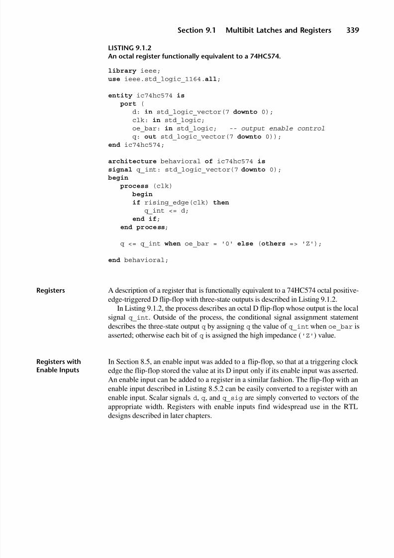
8/9/2019 VHDL for Engineers - Kenneth L. Short.pdf
http://slidepdf.com/reader/full/vhdl-for-engineers-kenneth-l-shortpdf 372/719
Section 9.1 Multibit Latches and Registers 339
LISTING 9.1.2An octal register functionally equivalent to a 74HC574.
library ieee;use ieee.std_logic_1164.all;
entity ic74hc574 isport (
d: in std_logic_vector(7 downto 0);clk: in std_logic;oe_bar: in std_logic; -- output enable controlq: out std_logic_vector(7 downto 0));
end ic74hc574;
architecture behavioral of ic74hc574 is
signal q_int: std_logic_vector(7 downto 0);begin
process (clk)begin
if rising_edge(clk) then
q_int <= d;end if;
end process;
q <= q_int when oe_bar = '0' else (others => 'Z');
end behavioral;
Registers A description of a register that is functionally equivalent to a 74HC574 octal positive-edge-triggered D flip-flop with three-state outputs is described in Listing 9.1.2.
In Listing 9.1.2, the process describes an octal D flip-flop whose output is the localsignal q_int. Outside of the process, the conditional signal assignment statementdescribes the three-state output q by assigning q the value of q_int when oe_bar isasserted; otherwise each bit of q is assigned the high impedance ('Z') value.
Registers withEnable Inputs
In Section 8.5, an enable input was added to a flip-flop, so that at a triggering clock edge the flip-flop stored the value at its D input only if its enable input was asserted.
An enable input can be added to a register in a similar fashion. The flip-flop with anenable input described in Listing 8.5.2 can be easily converted to a register with anenable input. Scalar signals d, q, and q_sig are simply converted to vectors of theappropriate width. Registers with enable inputs find widespread use in the RTLdesigns described in later chapters.

8/9/2019 VHDL for Engineers - Kenneth L. Short.pdf
http://slidepdf.com/reader/full/vhdl-for-engineers-kenneth-l-shortpdf 373/719
340 Chapter 9 Multibit Latches, Registers, Counters, and Memory
9 . 2 SH I FT R E G I S T E R S
Bits stored in a simple shift register are shifted one bit position (right or left) ateach triggering clock edge. If the shift is to the right, all bits are shifted one
position to the right, the input value is shifted into the leftmost bit position, and theoriginal value in the rightmost bit position is shifted out of the register. Theprimary uses for shift registers are serial-to-parallel conversion, parallel-to-serialconversion, and synchronous delay.
A shift register that shifts in only one direction is easily implemented by connectingthe Q output of one flip-flop to the D input of the next flip-flop in the direction of theshift (Figure 9.2.1). Each flip-flop in a shift register (and any logic associated with theflip-flop) is referred to as a stage.
In Figure 9.2.1, the input data is shifted into the leftmost stage at each triggeringclock edge. Data in the rightmost stage is shifted out. Data at input SI appears atoutput SOUT four clock cycles later. In this sense, an n-stage shift register can be
thought of as implementing a n clock period synchronous delay.
Shift registers are not constructed from D latches, because doing so would requirethat the clock pulse width be very precisely controlled. If the clock pulse were toowide, data would shift through multiple stages during one clock cycle.
Shift Register Usinga Buffer Mode Port
A description of a 4-bit right shift register with a synchronous clear input and buffermode outputs is given in Listing 9.2.1.
This shift register’s serial data input is si. Its serial output is taken fromqout(0). The parallel outputs of the shift register are qout(3) down to qout(0).
To describe the shift, we need to be able to read the present value in the shift register.If its mode is out, port qout cannot be directly read. Instead, qout is declared asmode buffer.
FIGURE 9.2.1
Shift register that shifts to the right.
Q3
D Q
CLK
SI
CLK
Q2
D Q
CLK
Q1
D Q
CLK
Q0
SOUTD Q
CLK

8/9/2019 VHDL for Engineers - Kenneth L. Short.pdf
http://slidepdf.com/reader/full/vhdl-for-engineers-kenneth-l-shortpdf 374/719
Section 9.2 Shift Registers 341
LISTING 9.2.1A 4-bit right shift register with synchronous clear using a buffer mode port.
library ieee;use ieee.std_logic_1164.all;
entity shiftreg_rb isport (si, clr_bar, clk : in std_logic;
qout : buffer std_logic_vector(3 downto 0));end shiftreg_rb;
architecture behavior of shiftreg_rb is
begin
process (clk)begin
if rising_edge(clk) then
if clr_bar = '0' then
qout <= "0000"; -- clear shift register else
qout(0) <= qout(1); -- shift rightqout(2) <= qout(3);qout(1) <= qout(2);qout(3) <= si;
end if;end if;
end process;end behavior;
Prior Restrictionson Mode Buffer Prior to IEEE Std 1076-2002 there was a restriction that, in a port map, a formal port of mode buffer could be associated with an actual that was itself a port only if the actualport was also of mode buffer. In practical terms, this meant that when an entity with aport of mode buffer was used as a component, it could only be connected to a signal orto a port of mode buffer of the enclosing entity. This limited the use of entities withbuffer mode ports as components. IEEE Std 1076-2002 removed this restriction. Theactual port associated with a formal port of mode buffer in a port map association isnow allowed to be mode out, inout, or buffer. However, some versions of simulatorsand synthesizers may still enforce the prior restrictions on ports of mode buffer.
Using a Signal
to Read a ModeOut Port
As a consequence of the prior restriction on mode buffer port associations, a local
signal was often used to allow the value assigned to a mode out port to be read(Figure 9.2.2). The signal is declared in the declarative part of the architecture and iswritten and read in the statement part of the architecture. At the end of the process,the value of this signal is assigned to the mode out port.

8/9/2019 VHDL for Engineers - Kenneth L. Short.pdf
http://slidepdf.com/reader/full/vhdl-for-engineers-kenneth-l-shortpdf 375/719
342 Chapter 9 Multibit Latches, Registers, Counters, and Memory
Shift RegistersUsing Readback
Signals
Accordingly, in Listing 9.2.2, signal q is declared and used as the shift registeroutput. Outside of the process, a concurrent signal assignment statement assigns the
value of q to port qout, which is mode out.
LISTING 9.2.2A 4-bit right shift register using a signal to “read” a mode out port.
library ieee;use ieee.std_logic_1164.all;
entity shiftreg_rs is
port (si, clr_bar, clk : in std_logic;qout : out std_logic_vector(3 downto 0));
end shiftreg_rs;
architecture behavior of shiftreg_rs is
signal q : std_logic_vector(3 downto 0);begin
process (clk)begin
if rising_edge(clk) then
if clr_bar = '0' then
q <= "0000"; -- clear shift register else
q(0) <= q(1); -- shift right
q(2) <= q(3);q(1) <= q(2);q(3) <= si;
end if;end if;
end process;qout <= q;
end behavior;
FIGURE 9.2.2
Using a signal to read the value assigned to an output port within an architecture.
Entity
Mode out port withsignal added for readback
signal added
for readback
Value
read

8/9/2019 VHDL for Engineers - Kenneth L. Short.pdf
http://slidepdf.com/reader/full/vhdl-for-engineers-kenneth-l-shortpdf 376/719
Section 9.2 Shift Registers 343
Order of“Sequential”Signal AssignmentStatements
In Listings 9.2.1 and 9.2.2, the sequences of assignment statements in the elseclauses are intentionally written in an order other than from the rightmost flip-flop tothe leftmost. For clarity, it would have been preferable that the assignments be listedin that order. Instead, they were listed in a random order. This was done to reinforcethe point that, since these are signal assignments, their values don’t change during
the current execution of the process (simulation cycle). Therefore, the order in whichthe flip-flop outputs are read and their values assigned does not matter.
Shift RegistersUsing Variables
Another technique to allow reading the value assigned to a port of mode out is to use avariable, rather than a signal. If a variable is used, the order of assignment to elementsof the variable vector is critical, because each assignment takes effect immediately.Assignments for a right shift must first assign variable q(1) to q(0), then q(2) toq(1), q(3) to q(2), and finally si to q(3), as shown in Listing 9.2.3.
LISTING 9.2.3A 4-bit right shift register using variables.
library ieee;use ieee.std_logic_1164.all;
entity shiftreg_rv is
port (si, clr_bar, clk : in std_logic;qout : out std_logic_vector(3 downto 0));
end shiftreg_rv;
architecture behavior of shiftreg_rv is
begin
clock: process (clk)variable q : std_logic_vector(3 downto 0);
begin
if rising_edge(clk) then
if clr_bar = '0' then -- clear shift register q := "0000";
else
q(0) := q(1); -- shift rightq(1) := q(2);q(2) := q(3);
q(3) := si;end if;qout <= q;
end if;end process;
end behavior;

8/9/2019 VHDL for Engineers - Kenneth L. Short.pdf
http://slidepdf.com/reader/full/vhdl-for-engineers-kenneth-l-shortpdf 377/719
344 Chapter 9 Multibit Latches, Registers, Counters, and Memory
Any change in the order of the assignments to variables in the else clause resultsin a design that doesn’t function correctly, because the contents of one or morestages of the shift register are overwritten before they are read. The shift registerdescriptions in Listings 9.2.1, 9.2.2, and 9.2.3 all synthesize to the same logic.
Use of theConcatenationOperator to Shift
A shift operation can be written more concisely using the concatenation operator andslices. Recall that the concatenation operator is predefined for all one-dimensionalarray types. The sequence of instructions
q(0) := q(1); -- shift rightq(1) := q(2);q(2) := q(3);q(3) := si;
can be replaced by a single assignment statement:
q := si & q(3 downto 1); -- shift right
This assignment takes the values in the leftmost three bit positions, prior to thetriggering clock edge, and appends them to the right of the serial input value tocreate a right shifted result that is assigned to q. That is, si is assigned to q(3) andslice q(3) down to q(1) is assigned to q(2) down to q(0).
Shift RegisterDigital Noise Filter
Figure 9.2.3 shows a logic representation of a digital noise filter. The purpose of thisfilter is to reject short-duration noise spikes at its data input cx. The filter’s output ycan change only after its input has had the same value at three consecutive triggeringclock edges. Input changes that have a duration of two or fewer clock cycles are
rejected (don’t cause a change in the output). Examination of the logic diagramindicates that a valid input change is delayed by five clock periods, one for eachflip-flop, before it is seen at the output.
A description of a functionally equivalent system is given in Listing 9.2.4.
FIGURE 9.2.3
Digital noise filter logic diagram.
CLK
Kcx
y
clk
D Q
CLKclk
D Q
CLKclk
D Q
CLKclk
D Q
CLKclk
J Q

8/9/2019 VHDL for Engineers - Kenneth L. Short.pdf
http://slidepdf.com/reader/full/vhdl-for-engineers-kenneth-l-shortpdf 378/719
Section 9.2 Shift Registers 345
LISTING 9.2.4Shift register digital filter.
library ieee;use ieee.std_logic_1164.all;
entity filter isport (cx, clk, rst_bar : in std_logic;
y : out std_logic);end;
architecture behavior of filter is
begin
synch: process (clk)variable q : std_logic_vector(3 downto 0);
begin
if rising_edge(clk) then
if rst_bar = '0' thenq := "0000";y <= '0';
else
if q(2 downto 0) = "111" then -- filter y <= '1';
elsif q(2 downto 0) = "000" then
y <= '0';else
null;end if;q := cx & q(3 downto 1); -- right shift
end if;end if;
end process;end behavior;
This code describes the functionality of the 4-bit shift register and J-K flip-flopwith gated inputs in Figure 9.2.3. The first flip-flop of the shift register is used toreduce the chances of a metastable event if the input data is asynchronous.
The filtered output is computed from the rightmost 3 bits of the shift register. If allthree of these bits are zeros "000", then output y is assigned a '0'. If all three of
these bits are ones "111", then y is assigned a '1'. For any other combination of these 3 bits, y remains unchanged.The filter operation is accomplished by the innermost if statement. The shift
operation is accomplished by the assignment statement for q that uses a concate-nation operation.

8/9/2019 VHDL for Engineers - Kenneth L. Short.pdf
http://slidepdf.com/reader/full/vhdl-for-engineers-kenneth-l-shortpdf 379/719
346 Chapter 9 Multibit Latches, Registers, Counters, and Memory
9 . 3 SHI FT RE G I ST ER CO UN T ER S
Using feedback, a shift register can be configured to produce a characteristicsequence of states. Such a shift register functions like a counter with a characteristic
count sequence and is often called a shift register counter . Two examples of shiftregister counters implemented by connecting their serial outputs back to their serialinputs are given in this section.
Johnson Counter A Johnson counter simply connects the complement of its serial output back to itsserial input. If a Johnson counter is cleared when reset, its serial output is 0. Since thecomplement of its serial output appears at its serial input, at each subsequent triggeringclock edge a 1 is shifted in, until the counter is filled with 1s. With its serial output nowa 1, a 0 is shifted in at each subsequent triggering clock edge, until the counter is filledwith 0s, making its serial output a 0. From this point, the count sequence repeats.
Counter Modulus The number of unique states a counter has is its modulus. The count (or statesequence) for a Johnson counter is 2 × n counts long (modulus 2 × n), where n is thenumber of stages in the shift register. A description of a 4-bit Johnson counter isgiven in Listing 9.3.1.
LISTING 9.3.1Johnson counter.
library ieee;use ieee.std_logic_1164.all;
entity jhnsncntr isport (clr_bar, clk : in std_logic;
qout : out std_logic_vector(3 downto 0));end;
architecture behavior of jhnsncntr is
begin
process (clk)variable q : std_logic_vector(3 downto 0);
begin
if rising_edge(clk) then
. if clr_bar = '0' then
q := "0000";else
q := not q(0) & q(3 downto 1); -- right shiftend if;
end if;qout <= q;
end process;end behavior;

8/9/2019 VHDL for Engineers - Kenneth L. Short.pdf
http://slidepdf.com/reader/full/vhdl-for-engineers-kenneth-l-shortpdf 380/719
Section 9.3 Shift Register Counters 347
In Listing 9.3.1, the assignment statement that accomplishes the right shiftassigns the complement of the serial output q(0) to the serial input:
q := not q(0) & q(3 downto 1); -- right shift
The resulting state sequence is shown in the waveforms in Figure 9.3.1.
Ring Counter A ring counter feeds its serial output directly back to its serial input. If at reset theshift register is loaded with a single 1, this 1 is shifted around the register over andover. The length of the count sequence is simply n. A description of a 4-bit ringcounter is given in Listing 9.3.2.
LISTING 9.3.2Ring counter.
library ieee;use ieee.std_logic_1164.all;
entity ringcntr is
port (rst_bar, clk : in std_logic;qout : out std_logic_vector(3 downto 0));
end;
architecture behavior of ringcntr is
begin
process (clk)
variable q : std_logic_vector(3 downto 0);begin
if rising_edge(clk) then
if rst_bar = '0' then
q := "1000";else
q := q(0) & q(3 downto 1); -- right shift(Cont.)
FIGURE 9.3.1
Output sequence from a 4-bit Johnson counter.

8/9/2019 VHDL for Engineers - Kenneth L. Short.pdf
http://slidepdf.com/reader/full/vhdl-for-engineers-kenneth-l-shortpdf 381/719
348 Chapter 9 Multibit Latches, Registers, Counters, and Memory
LISTING 9.3.2 (Cont.)
end if;end if;qout <= q;
end process;end behavior;
This code for the ring counter is essentially the same as that for the Johnsoncounter in Listing 9.3.1, except that this shift register is reset to “1000” and the serialoutput is fed back to the serial input without being complemented. The countsequence for this ring counter is illustrated in the waveforms in Figure 9.3.2. Eachpattern or codeword in the sequence has a single bit that is a 1. Such a set of codewords is referred to as a one-hot code.
9 . 4 C OU N TE R S
Counters are simple examples of finite state machines (FSMs). FSMs are discussedat length in Chapter 10. Counters are described more simply in this chapter.
Among other things, counters are used to count events, generate time intervals,generate events, and divide down an input signal to create a lower frequency outputsignal.
A counter’s next state is the state it goes to from its present state at a triggeringclock edge. A simple counter transitions from one unique state to another, until it
eventually returns to its initial state, after which its state transitions repeat.
Simple Counters The simplest counter has no inputs other than a clock and a reset. The counter’soutputs are taken directly from its flip-flops. After reset, the counter changes state ateach triggering clock edge.
FIGURE 9.3.2
Simulation waveforms for ring counter.

8/9/2019 VHDL for Engineers - Kenneth L. Short.pdf
http://slidepdf.com/reader/full/vhdl-for-engineers-kenneth-l-shortpdf 382/719
Section 9.4 Counters 349
Counter StateDiagram
The state transitions of a counter are clearly depicted by a state diagram. A statediagram for a 3-bit binary up counter is given in Figure 9.4.1. The counter isinitialized to 000 at reset and counts up to 111 before recycling to 000. A 3-bit binarycounter has a modulus of 8, or is, equivalently, a modulo-8 counter.
A 3-bit binary counter requires three flip-flops. The counter’s output consists of the Q outputs of its flip-flops. With n flip-flops we can create a counter with amodulus of up to 2n. Counters can also be designed to have a truncated sequence ortruncated modulus, so that the counter’s modulus is less than 2n.
SynchronousCounters
A synchronous counter is one in which all the flip-flops are clocked simultaneouslyby a common clock signal. All counters and other FSMs considered in this book aresynchronous. Synchronous designs are easier to verify than asynchronous designs,particularly with respect to timing. In addition, most PLD architectures are not wellsuited to implementing asynchronous sequential systems.
Counting byAddition orSubtraction
A straightforward approach to the description of a counter involves use of arithmetic
operators. An up counter is simply a register whose value is incremented. Incre-menting a register is accomplished by adding 1 to its present value. A down counteris a register whose value is decremented. Decrementing a register is accomplished bysubtracting 1 from its present value.
Adding orSubtractingStd_logic_vectors
In VHDL, addition and subtraction operations are predefined for only the typesinteger, real, and time. Since we are using std_logic or std_logic_vector types forinputs and outputs, we cannot use the predefined + and – operators directly. Twoways to solve this problem are:
1. Use type integer signals or variables along with the predefined + and – operators,then use functions to convert the integer results to std_logic.
2. Use type unsigned from the package NUMERIC_STD, which also overloadsthe + and – operators for this type, then convert the unsigned results tostd_logic_vector.
FIGURE 9.4.1
State diagram for a 3-bit counter.
010001 011
110
111 101
100000

8/9/2019 VHDL for Engineers - Kenneth L. Short.pdf
http://slidepdf.com/reader/full/vhdl-for-engineers-kenneth-l-shortpdf 383/719
350 Chapter 9 Multibit Latches, Registers, Counters, and Memory
LISTING 9.4.1A 4-bit binary up counter using an integer signal.
library ieee;use ieee.std_logic_1164.all;use ieee.numeric_std.all;
entity counter_4bit is
port (clk, reset_bar: in std_logic;count: out std_logic_vector (3 downto 0));
end counter_4bit;
architecture behav_int of counter_4bit is
signal count_int : integer range 0 to 15;begin
cnt_int: process (clk, reset_bar)
beginif reset_bar = '0' then
count_int <= 0;elsif rising_edge(clk) then
if count_int = 15 then
count_int <= 0;else
count_int <= count_int + 1; --read and increment count_intend if;
end if;end process;
count <= std_logic_vector(to_unsigned(count_int,4));
end behav_int;
Counter Using anInteger Signal
The first approach uses an integer signal or a variable to represent the count and thepredefined + and – operators. An example is shown in Listing 9.4.1 for a 4-bit binaryup counter.
Signal count_int is declared as type integer with a range of 0 to 15. This rangeis consistent with that of a 4-bit binary counter. Signal count_int maintains thecounter’s value and is incremented by the process at each triggering clock edge. Use
of signal count_int is another example of the previously introduced techniqueused to read the value assigned to a mode out port.
CounterInitialization
A counter, like any other FSM, needs to be initialized to operate properly. However, anIEEE Std 1076.6 compliant synthesizer ignores initial values in declarations. It does sobecause it cannot know whether the initialization specified can be accomplished atpower on reset in the target PLD. Accordingly, proper initialization requires the

8/9/2019 VHDL for Engineers - Kenneth L. Short.pdf
http://slidepdf.com/reader/full/vhdl-for-engineers-kenneth-l-shortpdf 384/719
Section 9.4 Counters 351
inclusion of either a reset or a load input (or both). A reset input can be asynchronousor synchronous, as desired. The VHDL code for a counter reset is similar to that usedfor a single flip-flop or for a multibit register.
The process in Listing 9.4.1 is sensitive to clk and reset_bar. If an eventoccurs on either clk or reset_bar, the process is executed. If reset_bar is '0',
then count_int is assigned the value 0, asynchronously resetting the counter.If the counter is not reset and there is a rising edge on clk, the present value of
count_int is checked to see if it is equal to 15. If so, then count_int is already atits maximum value and incrementing it must cause it to roll over to 0. If this check isnot made, count_int will increment from 15 to 16 and be out of its declared range(and the range of a 4-bit counter). This would cause a dynamic semantic error, whichwould be detected during simulation. If count_int is not equal to 15, then it isincremented by 1.
The outer if statement has no else clause and, therefore, infers a register. Theinferred register must have the number of bits necessary to represent an integer aslarge as 15 encoded in binary. Accordingly, the synthesizer infers a 4-bit register.
CounterRepresented as aRegister and Adder
A technology independent representation of the inferred logic is shown in Figure 9.4.2.Part of the counter is a 4-bit register. The input to this register is from a 4-bit
adder. The adder’s inputs are the signal count_int and a constant of value 1. Theadder symbol is a circle with a + sign inside. At each triggering clock edge, the sumof the present value in the register and the constant 1 is loaded into the register,producing the effect of a counter.
Signal count_int is needed for two reasons. First, we want an integer signal sothat we can use the predefined + operator. This integer signal is then converted to astd_logic_vector for output. Second, in order to increment this signal, we need to beable to read the present value of the counter. We can’t read that value directly fromcount, because count is a mode out port.
The concurrent assignment statement
count <= std_logic_vector(to_unsigned(count_int,4));
first uses the function to_unsigned to convert integer signal count_int into a4-bit unsigned vector. The value returned by this function is then converted to type
FIGURE 9.4.2
Hierarchical representation of synthesized 4-bit counter.
count_int[3:0]
[3:0]Q[3:0]
[29:32]9:32]D[3:0]
un9_count_int[29:32]
[3:0]
1count[3:0]
[3:0]
clk

8/9/2019 VHDL for Engineers - Kenneth L. Short.pdf
http://slidepdf.com/reader/full/vhdl-for-engineers-kenneth-l-shortpdf 385/719
352 Chapter 9 Multibit Latches, Registers, Counters, and Memory
std_logic_vector and assigned to output count. Since this assignment statement is aconcurrent function call, it executes anytime there is an event on the parametercount_int of the function to_unsigned.
Counter UsingUnsigned Signal
The second approach to describing a counter is simpler and more direct. A signal isagain used, but its type is unsigned.
A description of a 4-bit counter using an unsigned signal is given in Listing 9.4.2.The count is incremented by the statement:
count_us <= count_us + 1;
In this statement, the integer 1 is added to unsigned signal count_us. PackageNUMERIC_STD overloads the + operator so that it can be used to add an unsignedtype to a natural type. This package also overloads the + operator so that it can addtwo unsigned types. So this statement could also have been written as:
count_us <= count_us + "0001";
LISTING 9.4.2A 4-bit binary counter using an unsigned signal.
library ieee;use ieee.std_logic_1164.all;use ieee.numeric_std.all;
entity counter_4bit is
port (clk, reset_bar: in std_logic;
count: out std_logic_vector (3 downto 0));end counter_4bit;
architecture behav_us of counter_4bit is
signal count_us : unsigned(3 downto 0);
begin
cnt_us: process (clk, reset_bar)begin
if reset_bar = '0' thencount_us <= "0000";
elsif rising_edge(clk) then
count_us <= count_us + 1;end if;
end process;

8/9/2019 VHDL for Engineers - Kenneth L. Short.pdf
http://slidepdf.com/reader/full/vhdl-for-engineers-kenneth-l-shortpdf 386/719
Section 9.4 Counters 353
count <= std_logic_vector(count_us);
end behav_us;
Advantage of UsingType Unsignedfor Counting
An advantage of using an unsigned type in a binary counter is that we do not have tocheck whether the count is at its maximum value to force it to 0 on the next count.An unsigned vector naturally rolls over to 0 on the next count after it has reached all1s (2n – 1).
Counter Usinga Variable
Instead of using a signal to hold the count, we can use a variable. Listing 9.4.3describes a 4-bit binary counter using an unsigned variable.
Listing 9.4.3 reinforces an important concept regarding variables. A variable main-
tains its value between executions of a process (except for a variable declared in a
subprogram).
All three of the previous descriptions of a 4-bit counter create the same logicwhen synthesized.
LISTING 9.4.3A 4-bit binary counter using an unsigned variable.
library ieee;use ieee.std_logic_1164.all;use ieee.numeric_std.all;
entity counter_4bit is
port (clk, reset_bar: in std_logic;count: out std_logic_vector (3 downto 0));
end counter_4bit;
architecture behav_var of counter_4bit is
begin
cnt_var: process (clk, reset_bar)variable count_v : unsigned(3 downto 0);
begin
if reset_bar = '0' then
count_v := "0000";elsif rising_edge(clk) then
count_v := count_v + 1;end if;count <= std_logic_vector(count_v);
end process;end behav_var;

8/9/2019 VHDL for Engineers - Kenneth L. Short.pdf
http://slidepdf.com/reader/full/vhdl-for-engineers-kenneth-l-shortpdf 387/719
354 Chapter 9 Multibit Latches, Registers, Counters, and Memory
Down Counters Any of the previous binary counters can be changed to a down counter by replacingthe + operator with the – operator. If the counter uses an integer to hold the count,then a check must be made to determine if the present count is 0. If so, then the nextcount must be equal to 2n – 1 (all 1s in binary).
Up/Down Counters A control input can be added to make an up/down counter, which can count in eitherdirection. For example, an up input could be added. When a triggering clock edge isdetected, the inner if would determine if up = '1'. If so, the counter is incremented.If not, the counter is decremented.
Of course, we can easily create counters that count by values other than 1. Also,the amount an up/down counter increments can be different from the amount itdecrements.
Up/Down Counterwith an Enable
Input
A count enable input can also be added to a counter, so the counter only counts at atriggering clock edge when it is enabled. If the counter is not enabled, its count
remains the same at the triggering clock edge.A 12-bit binary up/down counter with a count enable input and a synchronous
reset is described in Listing 9.4.4. This counter’s count direction can be reversed atany point in its count sequence.
LISTING 9.4.4A 12-bit binary counter with count enable and synchronous reset.
library ieee;use ieee.std_logic_1164.all;use ieee.numeric_std.all;
entity binary_cntr is
port (clk, cnten, up, rst_bar: in std_logic;q: out std_logic_vector (11 downto 0));
end binary_cntr;
architecture behavioral of binary_cntr is
begin
cntr: process (clk)variable count_v : unsigned(11 downto 0);
begin
if rising_edge(clk) thenif rst_bar = '0' then
count_v := (others => '0');elsif cnten = '1' then
case up is
when '1' => count_v := count_v + 1; when others => count_v := count_v - 1;
end case;

8/9/2019 VHDL for Engineers - Kenneth L. Short.pdf
http://slidepdf.com/reader/full/vhdl-for-engineers-kenneth-l-shortpdf 388/719
Section 9.4 Counters 355
end if;end if;q <= std_logic_vector(count_v);
end process;end behavioral;
If an event on clk is a positive edge, the inner if statement determines if thecounter should be reset. If not, the count enable signal cnten is checked todetermine whether the counter is enabled to count. If so, a case statement deter-mines whether to count up or down. If the counter is not enabled to count, its valueremains unchanged.
Loading anInitial Value
Sometimes the initial state of a counter needs to be a value other than 0. Anotherapproach to providing an initial state, one that solves this problem, is to provide aload input. If such an input is synchronous, then, when it is asserted and a triggeringclock edge occurs, instead of incrementing (or decrementing), a predefined value isloaded into the counter.
TruncatedSequence Counters
A truncated sequence counter counts through a sequence that is not a power of 2. If at a triggering clock edge the present count is the last count desired in the sequence,the counter is loaded with the starting (initial) count value, instead of being incre-mented to the next binary count.
Frequency Divider A truncated sequence down counter is often used as a programmable frequency
divider (Listing 9.4.5).
LISTING 9.4.5Modulo m counter used for frequency division.
library ieee;use ieee.std_logic_1164.all;use ieee.numeric_std.all;
entity freq_div is
port (clk, reset_bar: in std_logic;divisor: in std_logic_vector(3 downto 0);q: out std_logic);
end freq_div;
architecture behavioral of freq_div is
begin
div: process (clk)variable count_v : unsigned(3 downto 0);
begin
(Cont.)

8/9/2019 VHDL for Engineers - Kenneth L. Short.pdf
http://slidepdf.com/reader/full/vhdl-for-engineers-kenneth-l-shortpdf 389/719
356 Chapter 9 Multibit Latches, Registers, Counters, and Memory
LISTING 9.4.5 (Cont.)
if rising_edge(clk) then
if reset_bar = '0' then
count_v := unsigned(divisor);q <= '0';
else
case count_v is
when "0010" =>count_v := count_v - 1;q <= '1'; when "0001" =>count_v := unsigned(divisor);q <= '0'; when others =>count_v := count_v - 1;q <= '0';
end case;end if;
end if;end process;
end behavioral;
The counter in Listing 9.4.5 counts the input load value (divisor) down by oneat each triggering clock edge. When the present count is "0010" at a triggeringclock edge, the count goes to "0001" and simultaneously output q becomes '1'.When the present state is "0001", the counter loads the value of divisor at thenext triggering clock edge and simultaneously q becomes '0'.
In effect, q functions as a terminal count signal. The '1' output at q lasts until thenext triggering clock edge, at which time q becomes'0'. Thus, the duration of the pulseat q is equal to one clock period. It takes a number of clock cycles equal to the value of divisor to produce one pulse at q. The overall effect is that the frequency of output qis 1/divisor times the frequency of the clock. Figure 9.4.3 shows the waveforms for adivisor of value 3.
Variable count_v, which maintains the count, never actually has the value "0000".Instead, the case statement checks whether count_v is "0001" at a triggering clock edge occurs. If this is true, count_v is assigned the value of divisor. This is equiv-alent to counting the value of count_v down, determining that its new value is
"0000", and reloading count_v with the value of divisor, all in one clock cycle.
BCD Counters A two-digit (two-decade) BCD counter is described in Listing 9.4.6. Since it countsin decimal, a two-digit BCD counter counts from 00 decimal to 99 decimal. On thenext count, it rolls over to 00 decimal.

8/9/2019 VHDL for Engineers - Kenneth L. Short.pdf
http://slidepdf.com/reader/full/vhdl-for-engineers-kenneth-l-shortpdf 390/719
Section 9.4 Counters 357
The least significant four bits of the counter represent the least significant decimaldigit (0 to 9) encoded in BCD. The most significant four bits represent the mostsignificant decimal digit, encoded in BCD. Since a BCD digit ranges from 0000 to1001 in binary, when the counter’s value is 00001001 (09 decimal), its value on thenext count must change to 00010000 (10 decimal).
LISTING 9.4.6Two-digit BCD counter.
library ieee;use ieee.std_logic_1164.all;use ieee.numeric_std.all;
entity counter_bcd is
port (clk, reset: in std_logic;count: out std_logic_vector (7 downto 0));
end counter_bcd;
architecture behavioral of counter_bcd is
begin
cnt: process (clk, reset)variable low_digit_v, high_digit_v : unsigned(3 downto 0);
beginif reset = '1' then
low_digit_v := b"0000";high_digit_v := b"0000";
(Cont.)
FIGURE 9.4.3
Waveforms for a divide-by-3 frequency divider.

8/9/2019 VHDL for Engineers - Kenneth L. Short.pdf
http://slidepdf.com/reader/full/vhdl-for-engineers-kenneth-l-shortpdf 391/719
358 Chapter 9 Multibit Latches, Registers, Counters, and Memory
LISTING 9.4.6 (Cont.)
elsif rising_edge(clk) then
low_digit_v := low_digit_v + 1; -- increment low digitif low_digit_v = b"1010" then -- low digit > 9?
low_digit_v := b"0000"; -- yes, make low digit = 0high_digit_v := high_digit_v + 1; -- increase high digit by 1
else
null;end if;if high_digit_v = b"1010" then -- high digit > 9?
high_digit_v := b"0000"; -- yes, make high digit 0else
null;end if;
end if;count(3 downto 0) <= std_logic_vector(low_digit_v);
count(7 downto 4) <= std_logic_vector(high_digit_v);end process;
end behavioral;
In Listing 9.4.6, two unsigned variables are declared, one for the low digit andone for the high digit. The outer if statement first checks to see if reset is asserted.If so, the low- and high-digit variables are set to 0.
If reset is not asserted, the elsif branch of the outer if statement checks for arising clock edge. At a rising clock edge, the low-digit variable is incremented. The
first inner if statement then checks to see if the low digit was incremented to 1010(10 decimal). If so, the low-digit variable is assigned the value 0000 (0 decimal) andthe high-digit variable is incremented.
The second inner if statement checks to see if the high digit was incremented to1010 (10 decimal). If so, the high digit is assigned the value 0000 (0 decimal).
At the end of the process, the values of these variables are assigned to the outputport signal in two slices:
count(3 downto 0) <= std_logic_vector(low_digit_v);count(7 downto 4) <= std_logic_vector(high_digit_v);
Modulo-32 BCDCounter
As a last counter example in this section, we consider a modulo-32 BCD counter.This two-digit BCD counter counts from 00 to 31 and then rolls over to 00. Thecount direction can be up or down. The counter has two count enable inputs; bothmust be asserted for the counter to count. Integer variables are used to store thecount.
The counter description is given in Listing 9.4.7.

8/9/2019 VHDL for Engineers - Kenneth L. Short.pdf
http://slidepdf.com/reader/full/vhdl-for-engineers-kenneth-l-shortpdf 392/719

8/9/2019 VHDL for Engineers - Kenneth L. Short.pdf
http://slidepdf.com/reader/full/vhdl-for-engineers-kenneth-l-shortpdf 393/719
360 Chapter 9 Multibit Latches, Registers, Counters, and Memory
LISTING 9.4.7 (Cont.)
else
bcd0_v := bcd0_v - 1;end if;
end if;end if;
end if;qbcd0 <= std_logic_vector(to_unsigned(bcd0_v, 4));qbcd1 <= std_logic_vector(to_unsigned(bcd1_v, 4));
end process;end behavioral;
9 . 5 DE TE C T I N G N ON –C LOC K S IGN AL E DGE S
Detecting clock signal edges was discussed in Section 8.3. Often a design requiresthat some action be carried out when an event occurs on a signal other than the clock signal. Prior to IEEE Std 1076.6-2004, only one signal was allowed to be used as theclock in a process. As a result, a non-clock signal could not simply be treated like asecond clock signal so that its edge could be detected. IEEE Std 1076.6-2004 nowallows multiple clock signals in a process, as long as the occurrence of the clock edges is mutually exclusive.
Since some tools and target PLDs don’t support multiple clocks in a process, wewill look at an approach that uses a synchronous edge detector that requires only asingle clock to detect the occurrence of an edge on some other signal. A synchronous
edge detector generates a synchronous pulse of one clock duration whenever itdetects the required edge of a specified signal.
The logic of a synchronous edge detector is shown in Figure 9.5.1. The objectiveis to detect positive edges of signal a. To do this, a version of signal a delayed by one
FIGURE 9.5.1
Synchronous positive edge detector.
a_delayed
R posedge.a_pe_2
a_pe
R
a_peclk
clr_bar
a QD QD

8/9/2019 VHDL for Engineers - Kenneth L. Short.pdf
http://slidepdf.com/reader/full/vhdl-for-engineers-kenneth-l-shortpdf 394/719
Section 9.5 Detecting Non–Clock Signal Edges 361
LISTING 9.5.1Positive edge detector system.
library ieee;use ieee.std_logic_1164.all;
entity posedge isport(
a : in std_logic;clr_bar : in std_logic;clk : in std_logic;a_pe : out std_logic);
end posedge;
architecture behavioral of posedge is
signal a_delayed : std_logic;begin
posedge: process (clr_bar, clk)begin
if clr_bar = '0' then
a_pe <= '0';a_delayed <= '0';
elsif rising_edge (clk) then
a_delayed <= a;a_pe <= not a_delayed and a;
end if;end process;
end behavioral;
clock cycle, called a_delayed, is created. This is done by storing a in a flip-flop ateach triggering clock edge. The complement of the delayed version of signal a isANDed with signal a itself. This AND function is a 1 only if a was 0 at the previoustriggering clock edge and is currently a 1. If the output of the AND is a 1, the outputof the edge detector (a_pe) becomes a 1 at the next triggering clock edge. Thus,a_pe is a '1' only if a positive edge occurred on a between the last two triggeringclock edges.
A description of a positive edge detector is given in Listing 9.5.1.This edge detector system detects each positive edge of signal a, as long as the
positive edge is not part of a narrow pulse that occurs between two adjacenttriggering clock edges. The operation of this system is illustrated by the waveformsin Figure 9.5.2. The narrow pulse that occurs just before 800 ns in Figure 9.5.2 ismissed because this pulse occurs between two triggering clock edges (one at 750 nsand the other at 850 ns).
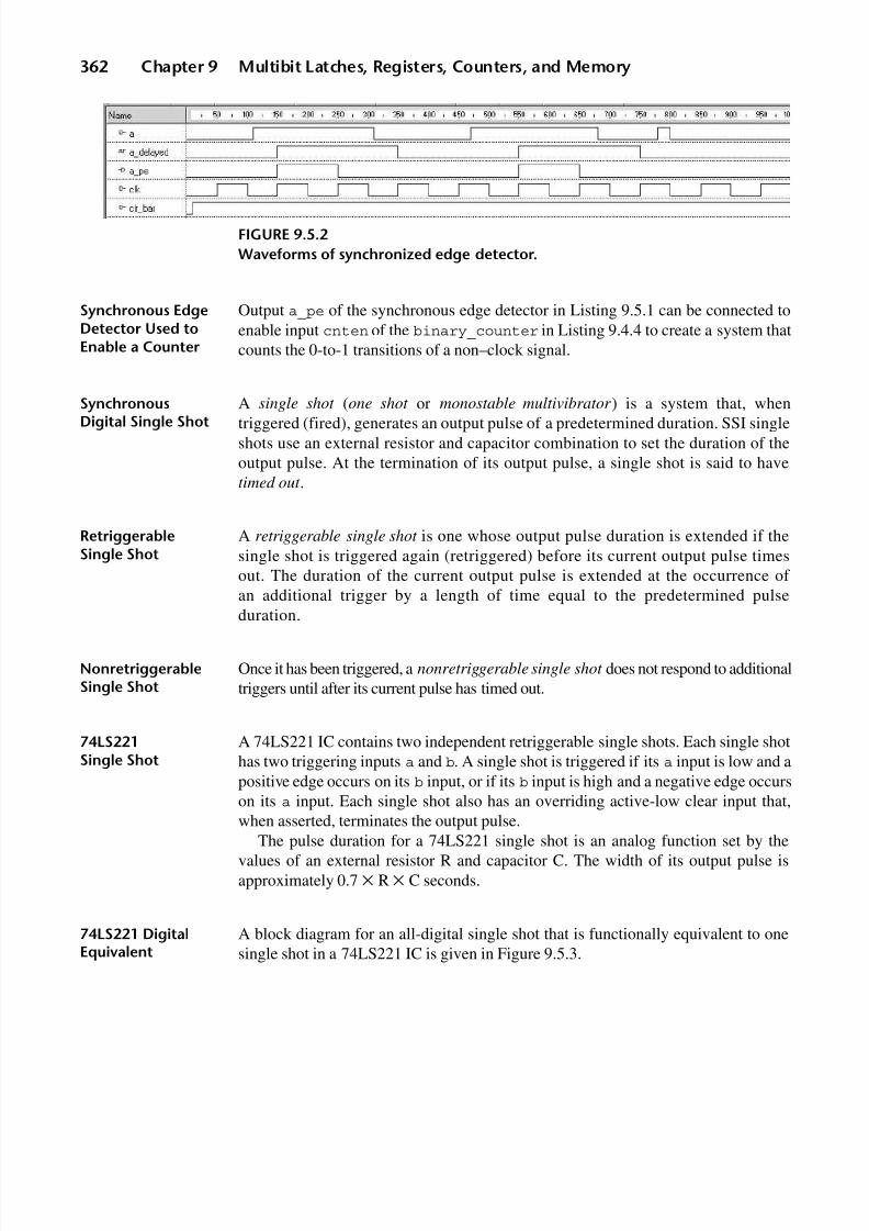
8/9/2019 VHDL for Engineers - Kenneth L. Short.pdf
http://slidepdf.com/reader/full/vhdl-for-engineers-kenneth-l-shortpdf 395/719
362 Chapter 9 Multibit Latches, Registers, Counters, and Memory
Synchronous EdgeDetector Used toEnable a Counter
Output a_pe of the synchronous edge detector in Listing 9.5.1 can be connected toenable input cnten of the binary_counter in Listing 9.4.4 to create a system thatcounts the 0-to-1 transitions of a non–clock signal.
SynchronousDigital Single Shot
A single shot (one shot or monostable multivibrator ) is a system that, whentriggered (fired), generates an output pulse of a predetermined duration. SSI singleshots use an external resistor and capacitor combination to set the duration of theoutput pulse. At the termination of its output pulse, a single shot is said to havetimed out .
RetriggerableSingle Shot
A retriggerable single shot is one whose output pulse duration is extended if thesingle shot is triggered again (retriggered) before its current output pulse timesout. The duration of the current output pulse is extended at the occurrence of an additional trigger by a length of time equal to the predetermined pulse
duration.
NonretriggerableSingle Shot
Once it has been triggered, a nonretriggerable single shot does not respond to additionaltriggers until after its current pulse has timed out.
74LS221Single Shot
A 74LS221 IC contains two independent retriggerable single shots. Each single shothas two triggering inputs a and b. A single shot is triggered if its a input is low and apositive edge occurs on its b input, or if its b input is high and a negative edge occurson its a input. Each single shot also has an overriding active-low clear input that,when asserted, terminates the output pulse.
The pulse duration for a 74LS221 single shot is an analog function set by thevalues of an external resistor R and capacitor C. The width of its output pulse isapproximately 0.7 × R × C seconds.
74LS221 DigitalEquivalent
A block diagram for an all-digital single shot that is functionally equivalent to onesingle shot in a 74LS221 IC is given in Figure 9.5.3.
FIGURE 9.5.2
Waveforms of synchronized edge detector.

8/9/2019 VHDL for Engineers - Kenneth L. Short.pdf
http://slidepdf.com/reader/full/vhdl-for-engineers-kenneth-l-shortpdf 396/719
Section 9.5 Detecting Non–Clock Signal Edges 363
Each of the blocks with rounded corners in Figure 9.5.3 is described by a separateprocess. The VHDL code is given in Listing 9.5.2 and combines a number of conceptspresented in this chapter. The triggering conditions are the same as for the 74LS221.However, instead of using an external resistor and capacitor to set the pulse duration, itis set by a constant. The single shot’s output pulse duration is the product of theconstant and the clock period.
LISTING 9.5.2Retriggerable single shot functionally similar to a 74LS221.
library ieee;use ieee.std_logic_1164.all;use ieee.numeric_std.all;
entity single_shot isport(
a : in std_logic;b : in std_logic;clr_bar : in std_logic;clk : in std_logic;q : out std_logic);
end single_shot;
architecture behavioral of single_shot is
signal a_delayed, b_delayed, fire_en : std_logic;
signal count : unsigned (7 downto 0);begin
delayed: process (clk)begin
if rising_edge (clk) then
a_delayed <= a;b_delayed <= b;
(Cont.)
FIGURE 9.5.3
Block diagram of processes for an all-digital retriggerable single shot.
a
b
clkdelayed
a_delayed
b_delayed
triggerfire_en
clk pulse_duration
load_value
reg_output
count
clk
clr_bar clr_bar
q

8/9/2019 VHDL for Engineers - Kenneth L. Short.pdf
http://slidepdf.com/reader/full/vhdl-for-engineers-kenneth-l-shortpdf 397/719
364 Chapter 9 Multibit Latches, Registers, Counters, and Memory
LISTING 9.5.2 (Cont.)
end if;end process;
trigger: process (a, a_delayed, b, b_delayed)variable a_tran, b_tran : std_logic_vector(1 downto 0);variable a_nedg, b_pedg : std_logic;
begin
a_tran := a_delayed & a; -- concatenate signals to form case expressionb_tran := b_delayed & b;
case a_tran is
when "10" => a_nedg := '1'; when others => a_nedg := '0';
end case;
case b_tran is when "01" => b_pedg := '1'; when others => b_pedg := '0';
end case;
fire_en <= (a_nedg and b) or (b_pedg and not a);end process;
pulse_duration: process(clk, clr_bar)constant load_value : unsigned := b"0000_0101";
begin
if clr_bar = '0' then
count <= (others => '0');elsif rising_edge (clk) then
if fire_en = '1' then
count <= load_value;else
if count /= b"0000_0000" then
count <= count - 1;end if;
end if;end if;
end process;
reg_output: process(clk, clr_bar)begin
if clr_bar = '0' then
q <= '0';elsif rising_edge (clk) then
if count /= b"0000_0000" then
q <= '1';

8/9/2019 VHDL for Engineers - Kenneth L. Short.pdf
http://slidepdf.com/reader/full/vhdl-for-engineers-kenneth-l-shortpdf 398/719
Section 9.5 Detecting Non–Clock Signal Edges 365
else
q <= '0';end if;
end if;end process;
end behavioral;
The description consists of four processes that communicate using the signalsa_delayed, b_delayed, fire_en, and count.
Process delayed generates the signals a_delayed and b_delayed, which areversions of signals a and b, respectively, delayed by one clock period. These signalsare used by process trigger.
Process trigger detects the required transitions in a and b and generates thesignal fire_en. Signal fire_en is asserted for one clock period whenever either of the conditions to fire the single shot are met. Note the creation of two vectors, one of
a_delayed concatenated with a and the other of b_delayed concatenated with b.These vectors are used in two case statements to determine the occurrence of therequired conditions to trigger the single shot.
Process pulse_duration counts out the predetermined duration of the outputpulse. If clr_bar is asserted, the counter is cleared. If not, clk is checked for a risingedge. If there is a rising edge on clk and fire_en is asserted, the counter isloaded with constant load_value, which determines the output pulse’s duration.If fire_en is not asserted and the counter’s value is not zero, then the counter isdecremented. If the single shot has been fired but has not timed out and fire_en
is again asserted (because the single shot has been retriggered), the counter is reloadedwith the constant value. This accomplishes the desired retriggering feature.
The process reg_out sets a flip-flop if the counter output is not 0 and clears theflip-flop if it is 0. This flip-flop’s output is the output of the single shot. A functionalsimulation of Listing 9.5.2, with constant load_value equal to five, is given inFigure 9.5.4.
The logic synthesized for Listing 9.5.2 is given in Figure 9.5.5.
FIGURE 9.5.4
Simulation waveforms for single shot.

8/9/2019 VHDL for Engineers - Kenneth L. Short.pdf
http://slidepdf.com/reader/full/vhdl-for-engineers-kenneth-l-shortpdf 399/719
366 Chapter 9 Multibit Latches, Registers, Counters, and Memory
9 .6 M IC RO PR OC ES SO R CO MP AT IB LE P UL SE WI D TH M O D U L A T E D S I G N A L G E N E R A T O R
A pulse width modulated (PWM) signal has a fixed period, but its duty cycle can bechanged (Figure 9.6.1).
There are many applications for PWM signals in electronic systems. A commonone is to control the speed of a DC motor. The PWM signal may be used to drive thegate of a HEXFET transistor that turns the motor ON when the signal is 1 and OFFwhen it is 0. If the period of the PWM signal is sufficiently short, the motor’s speedis proportional to the signal’s duty cycle. If the period of the PWM signal is toolarge, the motor’s speed is no longer controlled by the average value of the PWMsignal. Instead, the motor runs full speed when the PWM signal is a 1 and will,
eventually, stop when it is a 0.
FIGURE 9.5.5
Logic synthesized for single shot.
count[2:0]
R
Q[2:0]D[2:0]
count_5[2:0]
0
1
un1_count[5:7]
q
RQD
pulse_duration_un1_un1_un1_count
fire_en
trigger_un3_fire_en
trigger_fire_enb_delayed
QD
a_delayed
QD
q
clk
clr_bar
b
a
FIGURE 9.6.1
Pulse width modulated signal waveforms: (a) 20% duty cycle, (b) 40% dutycycle, (c) 90% duty cycle.
(a)
(b)
(c)

8/9/2019 VHDL for Engineers - Kenneth L. Short.pdf
http://slidepdf.com/reader/full/vhdl-for-engineers-kenneth-l-shortpdf 400/719
Section 9.6 Microprocessor Compatible Pulse Width Modulated Signal Generator 367
In this section, a microprocessor compatible PWM signal generator (PWMSG)design based on counter and register functions is presented. The PWMSG isdesigned to be interfaced to the bus of a microprocessor. The microprocessor writesa data byte to the PWMSG to specify the duty cycle. The PWMSG then generates anoutput signal with the specified duty cycle. The output signal’s duty cycle remains
constant until the microprocessor writes a new data byte to the PWMSG.A block diagram of the system is given in Figure 9.6.2. The microprocessor’s clock,
clk, is used to drive the clock input of the PWMSG. A prescalar divides down themicroprocessor clock to create a lower frequency signal, ps. This lower frequencysignal is used as the enable to the period counter, which, when enabled, counts at thetriggering edge of the microprocessor clock.
The 8-bit period counter sets the period of the PWM signal to be equal to 256times the period of the prescalar output ps. The period counter’s output period_cntis an 8-bit value that continuously cycles from 0 to 255 in binary. The time it takesperiod_cnt to cycle from 0 through 255 and then roll over to 0 determines oneperiod of the PWM output signal pwm_out.
The duty cycle subsystem contains an 8-bit register, duty_cycle. This register iswritten by the microprocessor to control the duty cycle. The microprocessor’s databus provides the data to be written at the data input of the duty cycle subsystem andcontrols the write operation using the cs_bar and we_bar inputs. The duty cycle of pwm_out is equal to the value written to the duty_cycle subsystem divided by256. For example, to obtain a 25% duty cycle the microprocessor must write thevalue 64 to the duty_cycle register.
The comparator compares the 8-bit value period_cnt from the period counterwith the 8-bit contents of register duty_cycle. If period_cnt is less than duty_
cycle, then pwm_out is a '1'; otherwise, it is a '0'.
Listing 9.6.1 is the description corresponding to Figure 9.6.2.
FIGURE 9.6.2
Microprocessor compatible pulse width modulated signal generator.
Prescalar Period
Counter
Duty
Cycle
Comparator
clk
reset
clk
reset
ps
clk
reset
we_bar
cs_bar
period_cnt
duty_cycle
pwm_out
8
8
data
clk

8/9/2019 VHDL for Engineers - Kenneth L. Short.pdf
http://slidepdf.com/reader/full/vhdl-for-engineers-kenneth-l-shortpdf 401/719
368 Chapter 9 Multibit Latches, Registers, Counters, and Memory
LISTING 9.6.1Pulse width modulated signal generator.
library ieee;use ieee.std_logic_1164.all;use ieee.numeric_std.all;
entity pwm isport (
data: in std_logic_vector (7 downto 0);cs_bar: in std_logic;we_bar: in std_logic;clk: in std_logic;reset: in std_logic;pwm_out: out std_logic);
end pwm;
architecture behavioral of pwm is
signal ps : std_logic;signal period_cnt : std_logic_vector(7 downto 0);signal duty_cycle : std_logic_vector(7 downto 0);
begin
prescalar : process (clk)variable pscount_v : unsigned(7 downto 0);variable ps_v : std_logic;
begin
if rising_edge(clk) then
if reset = '1' then
pscount_v := "10000100";
ps_v := '0';else
case pscount_v is
when "00000001" =>pscount_v := "10000100";ps_v := '1'; when others =>pscount_v := pscount_v - 1;ps_v := '0';
end case;end if;
ps <= ps_v;end if;
end process;
period_cntr: process (clk)variable count_v : unsigned(7 downto 0);
begin
if rising_edge(clk) then

8/9/2019 VHDL for Engineers - Kenneth L. Short.pdf
http://slidepdf.com/reader/full/vhdl-for-engineers-kenneth-l-shortpdf 402/719
Section 9.6 Microprocessor Compatible Pulse Width Modulated Signal Generator 369
if reset = '1' then
count_v := (others => '0');elsif ps = '1' then
count_v := count_v + 1;end if;period_cnt <= std_logic_vector(count_v);
end if;end process;
duty : process (clk)begin
if rising_edge(clk) then
if reset = '1' then
duty_cycle <= (others => '0');elsif we_bar = '0' and cs_bar = '0' then
duty_cycle <= data;end if;
end if;end process;
comparator : process (clk)begin
if rising_edge(clk) then
if reset = '1' then
pwm_out <= '0';elsif period_cnt < duty_cycle then
pwm_out <= '1';else
pwm_out <= '0';end if;
end if;end process;
end behavioral;
Each subsystem in Figure 9.6.2 is described by a separate process. The fourprocesses communicate via signals. Each process describes a sequential subsystemthat is clocked by the microprocessor clock.
These four processes are modifications of previous designs. The prescalar process
is a variation of the frequency divider in Listing 9.4.5. The primary differencebetween them is that the divisor value was an input in the frequency divider designentity and is a constant for this prescalar. The value of the prescalar’s divisorconstant is determined based on the microprocessor’s clock frequency and thedesired period for pwm_out.
The period counter process is an 8-bit up counter with an enable. It is a simplifi-cation of the 12-bit up/down counter with an enable described in Listing 9.4.4.

8/9/2019 VHDL for Engineers - Kenneth L. Short.pdf
http://slidepdf.com/reader/full/vhdl-for-engineers-kenneth-l-shortpdf 403/719
370 Chapter 9 Multibit Latches, Registers, Counters, and Memory
The duty cycle process describes a simple 8-bit register with a synchronous loadcapability. If we_bar and cs_bar are both asserted at a triggering clock edge, theregister is loaded with the data from the microprocessor.
The comparator process describes a comparator that has a registered output. Thecomparator compares two 8-bit vectors and produces a '1' output as long as
period_cnt is less than duty_cycle; otherwise, the output is '0'.
Code Reuse The four processes in Listing 9.6.1, being variations of previous processes we havewritten, are examples of code reuse. The more code that we write, the more we findthat the functionality needed for new subsystems is similar to that of somesubsystem we designed in the past. The problem is keeping track of and maintainingthe processes that we have previously written so they can be reused.
Instead of using separate processes for each subsystem, we can use separate designentities and connect them in a structural architecture. The advantage of separatedesign entities is that they can be compiled to libraries, simplifying management of the code for reuse. This approach is used in later chapters.
9 . 7 ME MO RI E S
Earlier in this chapter, we considered memory structures that were individual multibitlatches or registers. These structures are one-dimensional arrays of memory elements(bits). In this section, we consider memories that consist of multiple multibit latchesor multiple registers. Such a memory is a single storage unit that consists of atwo-dimensional array of memory elements (Figure 9.7.1). This two-dimensionalarray of bits is equivalent to a one-dimensional array of multibit latches or registers.
To be uniquely identified, each multibit latch or register has an address.
MemoryOrganization
Bits in a single row (multibit latch or register) of the array comprise a word . All thebits in a word are written or read simultaneously.
FIGURE 9.7.1
Memory: (a) conceptual representation, (b) logic representation.
Address Data
0
1
2
3
45
6
7
address
data_in data_out
we_bar
oe_bar
(a) (b)
m
n n

8/9/2019 VHDL for Engineers - Kenneth L. Short.pdf
http://slidepdf.com/reader/full/vhdl-for-engineers-kenneth-l-shortpdf 404/719
Section 9.7 Memories 371
The external organization of a memory is expressed as the number of words × thenumber of bits per word in the memory. This is also referred to as the length × width,or depth × width, or aspect ratio of the memory. It is typically written as 2m × n,where m is the number of address inputs used to select a single word from the arrayof words and n is the number of data bits in each word. For example, a 16 × 8
memory contains 16 words each 8 bits wide. It has 4 address bits (inputs).
RAM and ROM Technically, RAM stands for random access memory. A random access memory isone in which the amount of time it takes to read (access) a word from any one address(location in the memory) is essentially the same as for reading from any otheraddress in the memory. This is in contrast to what is the case for a serial memory.However, the term RAM is commonly used to mean a memory that can be writtenand read during its normal operation. This is in contrast to read-only memory(ROM), which although random access, can only be read during its normal operation.A ROM’s contents are defined only once; therefore, a ROM stores constant values.
Asynchronous RAMUsing a Signal
A description of an 8 × 8 asynchronous RAM with separate data inputs and outputsis given in Listing 9.7.1.
LISTING 9.7.1Asynchronous RAM using a signal.
library ieee;use ieee.std_logic_1164.all;use ieee.numeric_std.all;
entity memory is
port(we_bar : in std_logic; -- write enableoe_bar : in std_logic; -- output enabledata_in : in std_logic_vector(7 downto 0);address : in std_logic_vector(2 downto 0);data_out : out std_logic_vector(7 downto 0));
end memory;
architecture behavioral of memory is
type mem_array is array (0 to 2**(address'length) - 1)of std_logic_vector (7 downto 0);
signal mem_s : mem_array;begin
write: process(we_bar, data_in, address)begin
if we_bar = '0' then
mem_s(to_integer(unsigned(address))) <= data_in;
(Cont.)

8/9/2019 VHDL for Engineers - Kenneth L. Short.pdf
http://slidepdf.com/reader/full/vhdl-for-engineers-kenneth-l-shortpdf 405/719
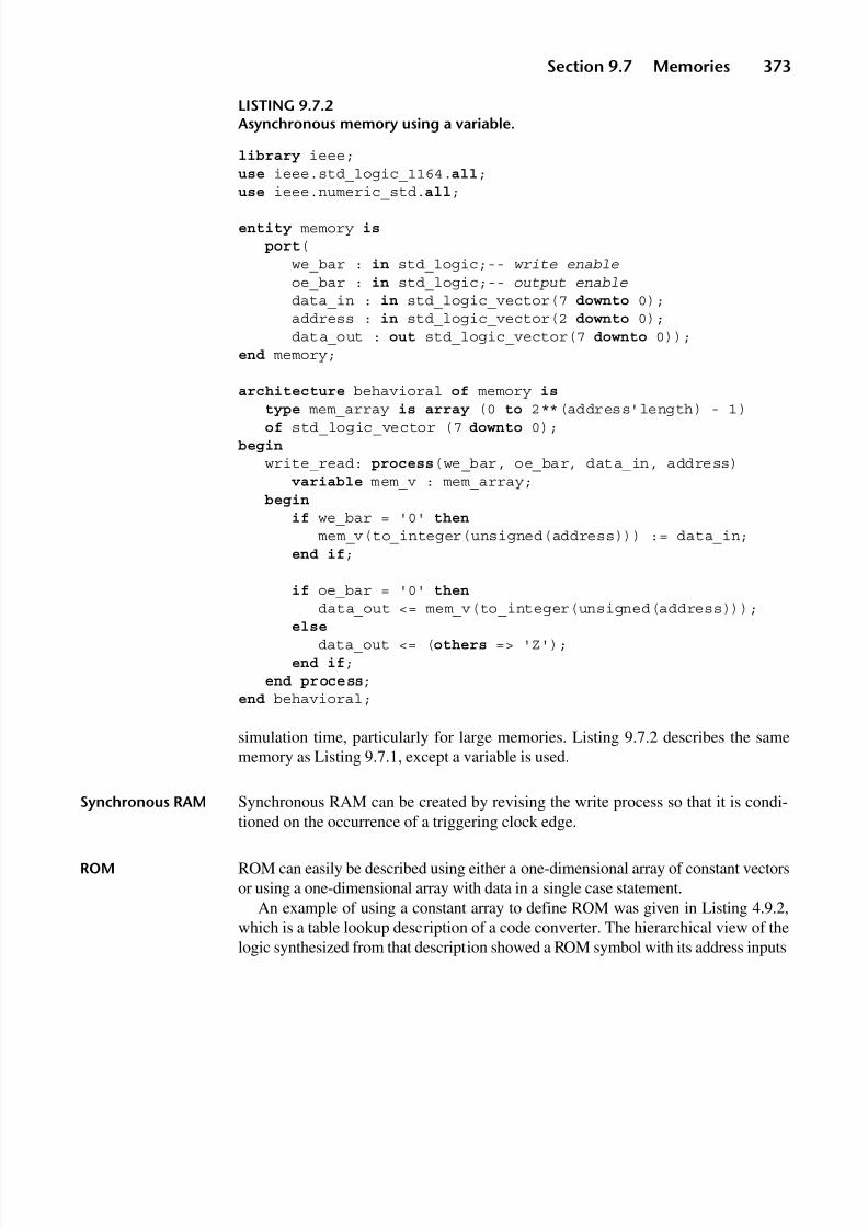
8/9/2019 VHDL for Engineers - Kenneth L. Short.pdf
http://slidepdf.com/reader/full/vhdl-for-engineers-kenneth-l-shortpdf 406/719
Section 9.7 Memories 373
LISTING 9.7.2Asynchronous memory using a variable.
library ieee;use ieee.std_logic_1164.all;use ieee.numeric_std.all;
entity memory is
port(we_bar : in std_logic;-- write enableoe_bar : in std_logic;-- output enabledata_in : in std_logic_vector(7 downto 0);address : in std_logic_vector(2 downto 0);data_out : out std_logic_vector(7 downto 0));
end memory;
architecture behavioral of memory is
type mem_array is array (0 to 2**(address'length) - 1)of std_logic_vector (7 downto 0);begin
write_read: process(we_bar, oe_bar, data_in, address)variable mem_v : mem_array;
begin
if we_bar = '0' then
mem_v(to_integer(unsigned(address))) := data_in;end if;
if oe_bar = '0' then
data_out <= mem_v(to_integer(unsigned(address)));else
data_out <= (others => 'Z');end if;
end process;end behavioral;
simulation time, particularly for large memories. Listing 9.7.2 describes the samememory as Listing 9.7.1, except a variable is used.
Synchronous RAM Synchronous RAM can be created by revising the write process so that it is condi-
tioned on the occurrence of a triggering clock edge.
ROM ROM can easily be described using either a one-dimensional array of constant vectorsor using a one-dimensional array with data in a single case statement.
An example of using a constant array to define ROM was given in Listing 4.9.2,which is a table lookup description of a code converter. The hierarchical view of thelogic synthesized from that description showed a ROM symbol with its address inputs

8/9/2019 VHDL for Engineers - Kenneth L. Short.pdf
http://slidepdf.com/reader/full/vhdl-for-engineers-kenneth-l-shortpdf 407/719

8/9/2019 VHDL for Engineers - Kenneth L. Short.pdf
http://slidepdf.com/reader/full/vhdl-for-engineers-kenneth-l-shortpdf 408/719
Problems 375
ratios. Memory elements in these block RAMs have been optimized for their intendedpurpose and are much more area efficient than RAM created by a synthesizer logicallycombining a PLD’s distributed memory elements (individual latches or flip-flops).
While some synthesizers can infer block RAM from RAM and ROM descriptionslike those in this section, it is more common to instantiate each block RAM as a
component. For a PLD with block RAM, the manufacturer provides parameterizedRAM and ROM components in a library. When a block RAM is instantiated,generics are used to specify its aspect ratio. Alternatively, the PLD manufacturermay provide a program that uses a wizard to generate the VHDL code for a block ram component from selections made in a menu.
Block RAM on a PLD can be used to implement RAM or ROM. When imple-menting ROM, values for the contents of the block RAM must be specified. Whenimplementing RAM, if values are specified for its contents, they are initial values.Block RAM contents are typically specified in a separate file in a format created forspecifying memory contents, such as Intel’s HEX format.
The drawback in instantiating block RAM from a PLD manufacturer’s library isthat the resulting design has limited portability to other target PLDs.
PROBLE MS
9.1 What is the characteristic of an interconnection of latches or flip-flops that make them form amultibit latch or register, respectively?
9.2 Rewrite Listing 8.5.2 to create a description of a positive-edge-triggered 8-bit register namedreg8_pe. This register has an asserted high enable input (en) and an asserted-low clear input(clear_bar).
9.3 Consult the data sheet for a 74HC573 octal transparent D latch with three-state outputs. Writea description of a functionally equivalent device. Use the same names for ports in yourdescription as the pin names used on the data sheet. If a pin name uses an overbar, use the samename with a _bar suffix. Specify the D inputs and Q outputs as vectors.
9.4 Consult the data sheet for a 100353 8-bit register. Write a description of a functionallyequivalent device. Use the same names for ports in your description as the pin names used onthe data sheet. If a pin name uses an overbar, use the same name with a _bar suffix. Specifythe D inputs and Q outputs as vectors.
9.5 A port of an entity is declared as mode out. The value output by the port must be read in theentity’s architecture to compute a new output value. How can this be accomplished withoutchanging the port’s mode?
9.6 In terms of when the output actually shifts, does the operation of the shift register in Listing9.2.2 change if the assignment statement qout <= q is placed immediately after:
(a) the inner if statement?(b) the outer if statement?
Base your analysis on how a simulator would simulate the description. Also, would a synthesizergenerate different logic for the three descriptions?
8/9/2019 VHDL for Engineers - Kenneth L. Short.pdf
http://slidepdf.com/reader/full/vhdl-for-engineers-kenneth-l-shortpdf 409/719
376 Chapter 9 Multibit Latches, Registers, Counters, and Memory
9.7 Examine Listing 9.2.4. If variableq were changed to a signal would the behavior of the systemremain the same? Provide an explanation to justify your answer.
9.8 Examine Listing 9.2.4. How is the operation of the system changed if the innermost if statement that describes the filter operation is interchanged with the assignment statementthat describes the right shift? Explain the differences in behavior in terms of VHDL’s
semantics.9.9 Examine Listing 9.2.4. How is the operation of the system changed if:
(a) the assignment statement that describes the right shift is moved up one line so that itprecedes the end if statement that closes the outermost if statement?
(b) the assignment statement that describes the right shift is moved up two lines so that itfollows the end if statement that closes the innermost if statement?
Explain any differences in behavior in terms of VHDL’s semantics.
9.10 Write a description for an 8-bit shift register. The shift register has a serial input ser_in anda serial output ser_out. The shift register also has eight parallel inputs din7 down to din0.The shift register is synchronously loaded from these inputs when its load input is asserted.The shift register also has a synchronous clear input clear. When its shift_r input isasserted the shift register shifts its contents one position to the right at the next positive edge atits clk input.
9.11 Consult the data sheet for a 74AC299 Universal Shift/Storage Register. Write a completeVHDL description of a functionally equivalent device. Use the same names for ports in yourdescription as the pin names used on the data sheet. If a pin name uses an overbar, use the samename with a _bar suffix attached. Specify IO0 to IO7 as a vector.
9.12 A fully synchronous doubler system is to be designed. This system can load an initial 10-bitvalue, and then double the value on each positive edge of the input clock, if the system’s enableinput is asserted. The doubled value is available as an output from the system. If the result afterdoubling exceeds 10 bits, then the overflow flag is set and the result modulo 2**10 (210) is
output. If an attempt is made to double the result after overflow, the output is made all 0s andthe overflow flag is cleared.
The entity declaration for the doubler system is:
entity doubler isport(
clk : in std_logic;-- clock inputenable : in std_logic;-- enable doubling inputload : in std_logic;-- enable loading of value to be doubledload_val : in std_logic_vector(9 downto 0); -- initial value to be doubledoverflow : out std_logic;-- overflow flag
q : out std_logic_vector(9 downto 0)-- doubled value);end doubler;
Write a behavioral architecture for the doubler design entity.
9.13 Write a description of a 4-bit ring counter named ring_cntr. ring_cntr circulates asingle 0 from right to left when it is enabled. Its asserted-low reset is synchronous. Thearchitecture that you create for this design entity must be behavioral. The entity declaration is:

8/9/2019 VHDL for Engineers - Kenneth L. Short.pdf
http://slidepdf.com/reader/full/vhdl-for-engineers-kenneth-l-shortpdf 410/719
Problems 377
entity ring_cntr isport (
rst_bar : in std_logic; -- reset active lowclk : in std_logic; -- clkenable : in std_logic; -- enable active highqout : out std_logic_vector(3 downto 0) -- output);
end;
9.14 Write a description of a 5-bit ring counter named ring_cntr5. When reset, design entityring_cntr5 contains the pattern 00011. The contents of this ring counter are circulated onebit position to the left when it is enabled. The asserted-low reset is synchronous. You mustcreate a behavioral style architecture. This design entity has the following entity declaration:
entity ring_cntr5 isport (
rst_bar : in std_logic; -- reset active low
clk : in std_logic; -- clkenable : in std_logic; -- enable active highqout : out std_logic_vector(4 downto 0) -- output);
end;
9.15 Write a description of a 4-bit up/down counter that does not overflow or underflow. When thecount reaches its maximum value it remains at that value if the count mode is up. When thecount reaches zero, it remains zero if the count mode is down. Use a control input named upto control the direction of the count.
9.16 Write a description of a 4-bit up counter named by1or2. The counter increments on a positiveclock edge only if its active low enable (cnten_bar) is asserted. If its by2 input is asserted,the counter increments by 2; otherwise, it increments by 1. If the counter overflows it continuesto count from 00000. The counter has an active-low asynchronous reset (rst_bar) and anactive-low synchronous clear (clr_bar).
9.17 A counter is to be designed that can count up or down when enabled. When counting up, thecounter counts in binary from 3 to 6 and repeats. When counting down, it counts from 6 downto 3 and repeats. When reset, the counter’s value is 3.
The entity declaration for the counter is:
entity cntr_trunc_seq isport(
clk : in std_logic; -- system clockcten_bar : in std_logic; -- enable countingup_bar : in std_logic; -- count directionrst_bar : in std_logic; -- synchronous resetcount : out std_logic_vector (2 downto 0) -- output count);
end cntr_trunc_seq;
Write a context clause and an architecture body for the counter.

8/9/2019 VHDL for Engineers - Kenneth L. Short.pdf
http://slidepdf.com/reader/full/vhdl-for-engineers-kenneth-l-shortpdf 411/719
378 Chapter 9 Multibit Latches, Registers, Counters, and Memory
9.18 Write a description of a frequency divider that produces an output fdiv that is equal to its inputclock frequency divided by a factor of either 3, 8, 12, or 16. The divisor value is selected by a2-bit input vector named divby. The division factor determined by divby is given in the table.
Ifdivby is changed, the current output period is completed before the new output period takeseffect.
9.19 Consult the data sheet for a 74HC191 counter. Write a design description of a functionallyequivalent device.
9.20 Modify the counter in Problem 9.19 to add an input bin that controls whether the counting is
one in binary or BCD.9.21 You must design a BCD synchronous up/down counter having the following entity declaration:
entity bcd_cntr isport(
clk : in std_logic; -- clockclear_bar : in std_logic; -- synchronous clear counterup_bar : in std_logic; -- count direction controlcten_bar : in std_logic; -- count enablemax_min_bar : out std_logic; -- 0 for maximum/minimum countqdcba : out std_logic_vector(3 downto 0) -- counter output);
end bcd_cntr;
Write a complete description of the counter. Use a process containing an if statement and usean integer signal to represent the count. The max_min_bar output is asserted when theoutput reaches the maximum count when counting up or reaches the minimum count whencounting down.
9.22 An event detector system indicates whether an event (positive or negative edge) has occurredon an input signal. If an event has occurred just prior to the last triggering clock edge, the outputis a 1 for one clock period; otherwise, it remains a 0. The entity declaration for the system is:
entity event_detector is
port( input : in std_logic; -- input clk : in std_logic; -- system clock rst_bar : in std_logic; -- asynchronous reset event : out std_logic -- output );end event_detector;
Write a behavioral design description of this entity.
divby divisor
00 301 8
10 12
11 16

8/9/2019 VHDL for Engineers - Kenneth L. Short.pdf
http://slidepdf.com/reader/full/vhdl-for-engineers-kenneth-l-shortpdf 412/719
Problems 379
9.23 A system needs to carry out an action for 0.5 seconds. To do this it will use a component calleddelay to measure the 0.5 s. When a positive edge occurs at its fire input, componentdelay generates a positive pulse of one clock cycle duration at its delayed_out output 0.5s later. Assume the system clock is 1 MHz and the system is to be fully synchronous. Write acomplete description of delay using a behavioral architecture body. This architecture bodymust be as simple as possible. Use an integer signal to count out the delay.
9.24 Assuming that the microprocessor provides an 8 MHz square wave forclk, what is the period,frequency, and duty cycle of the local signal ps and what is the period of the output signalpwm_out for the PWM signal generator of Listing 9.6.1?
9.25 The comparator process for the PWM signal generator in Listing 9.6.1 was written so that itsoutput is latched. Write a process description that provides an alternative purely combinationalcomparator subsystem. This combinational approach has simpler hardware since it does notinclude the output latch. Discuss the advantages and disadvantages of these two approaches interms of various applications (the subsystem driven by pwm_out).
9.26 What would be the effect on the simulation of the program in Listing 9.7.1 of leavingdata_in out of the sensitivity list of the write process? What would be the effect on the
synthesized logic of this omission?
9.27 Modify the program in Listing 9.7.1 to include a chip select input cs_bar. When cs_bar isasserted, the memory can be either written or read. When cs_bar is not asserted, no operationcan be carried out on the memory and its output is in its high-impedance state.
9.28 Modify the program in Listing 9.7.2 so that the memory has common data I/O; in other words,a single bidirectional data bus. In normal operation it would be assumed that both oe_bar andwe_bar are not simultaneously asserted. However, write your description so that if this werethe case, the write operation would predominate and RAM would not drive the data bus duringthis time.
9.29 Modify the program in Listing 9.7.2 to produce RAM that is written synchronously on a
positive clock edge, but is read asynchronously. This requires the addition of a clock signal,clk.
9.30 RAM can be both written and read synchronously. Modify the program in Listing 9.7.2 toproduce RAM that is both written and read synchronously on a positive clock edge.
9.31 Rewrite the ROM description in Listing 9.7.3 to use a variable to hold the ROM data.

8/9/2019 VHDL for Engineers - Kenneth L. Short.pdf
http://slidepdf.com/reader/full/vhdl-for-engineers-kenneth-l-shortpdf 413/719
380
Chapter 10
Finite State Machines
A sequential system is also known as a finite state machine (FSM). The FSMapproach to sequential system design is a straightforward generic approach thatallows any sequential system to be designed. In theory, a sequential system of anycomplexity can be designed as a single FSM. In practice, complex systems aredecomposed into components, where one or more are FSMs.
A FSM’s operation may be graphically represented by a state diagram. Devel-opment of a state diagram from a FSM’s specification is the first step in the FSM’sdesign.
After a brief review of FSM concepts and state diagrams, the VHDL descriptionof both Mealy and Moore type FSMs using a three-process approach is presented.One and two process approaches are also discussed.
During the development of a state diagram, states are usually represented bydescriptive names. If so, these same names are used in the FSM’s VHDL description.During synthesis, each state name must be replaced by a binary code. The choice of binary values to encode the states can be specified by the designer or left to thesynthesizer. The effect of this choice on the complexity of the synthesized logic isalso considered.
10 .1 F IN I TE S TA TE M AC H IN ES
A sequential system is a finite state machine (FSM). It is a digital system whoseoutputs are a function of both its present input values and its past history of inputvalues.

8/9/2019 VHDL for Engineers - Kenneth L. Short.pdf
http://slidepdf.com/reader/full/vhdl-for-engineers-kenneth-l-shortpdf 414/719
Section 10.1 Finite State Machines 381
State of a FSM Information characterizing the effect of a FSM’s past history of input values isprovided by its state. Physically, a FSM’s state is represented by the value stored in aregister called the state register . This value is referred to as the present state of thesystem or simply the state of the system.
SynchronousversusAsynchronousFSM
A sequential system may be either asynchronous or synchronous. An asynchronoussequential system has no clock and its state can change value as soon as any of itsinputs changes value. In contrast, a synchronous sequential system is controlled by asystem clock and its state can change value only at a triggering clock edge. In asynchronous system, asynchronous actions are limited to the external reset used toforce the synchronous system into an initial state at power on.
In theory asynchronous systems can operate faster and use less power. However,they are significantly more difficult to design and their successful operation is verydependent on the specific delays of their components. Furthermore, PLD architec-tures are not appropriate for implementing asynchronous systems.
Fully SynchronousFSM
The majority of sequential systems are synchronous and our interest is furtherlimited to fully synchronous systems. In a fully synchronous FSM all registers areclocked by a single clock signal. Synthesis tools perform well in synthesizing fullysynchronous designs. Thus, in this book, when the term FSM is used without elabo-ration, a fully synchronous FSM is assumed.
Inputs A FSM’s inputs are sampled at each triggering clock edge. Accordingly, a FSM’sinput sequence is ordered in time by its clock. Figure 10.1.1 is a block diagram of a
FIGURE 10.1.1
Fully synchronous finite state machine (FSM) block diagram.
Combinationallogic
S t a t e
R e g i s t e r
Inputs Outputs
next_statepresent_state
clock
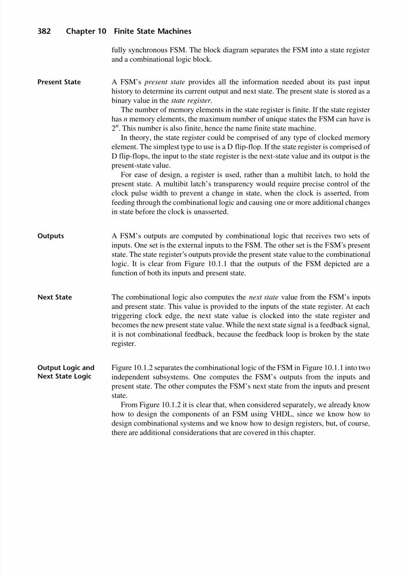
8/9/2019 VHDL for Engineers - Kenneth L. Short.pdf
http://slidepdf.com/reader/full/vhdl-for-engineers-kenneth-l-shortpdf 415/719
382 Chapter 10 Finite State Machines
fully synchronous FSM. The block diagram separates the FSM into a state registerand a combinational logic block.
Present State A FSM’s present state provides all the information needed about its past inputhistory to determine its current output and next state. The present state is stored as abinary value in the state register .
The number of memory elements in the state register is finite. If the state registerhas n memory elements, the maximum number of unique states the FSM can have is2n. This number is also finite, hence the name finite state machine.
In theory, the state register could be comprised of any type of clocked memoryelement. The simplest type to use is a D flip-flop. If the state register is comprised of D flip-flops, the input to the state register is the next-state value and its output is thepresent-state value.
For ease of design, a register is used, rather than a multibit latch, to hold thepresent state. A multibit latch’s transparency would require precise control of the
clock pulse width to prevent a change in state, when the clock is asserted, fromfeeding through the combinational logic and causing one or more additional changesin state before the clock is unasserted.
Outputs A FSM’s outputs are computed by combinational logic that receives two sets of inputs. One set is the external inputs to the FSM. The other set is the FSM’s presentstate. The state register’s outputs provide the present state value to the combinationallogic. It is clear from Figure 10.1.1 that the outputs of the FSM depicted are afunction of both its inputs and present state.
Next State The combinational logic also computes the next state value from the FSM’s inputsand present state. This value is provided to the inputs of the state register. At eachtriggering clock edge, the next state value is clocked into the state register andbecomes the new present state value. While the next state signal is a feedback signal,it is not combinational feedback, because the feedback loop is broken by the stateregister.
Output Logic andNext State Logic
Figure 10.1.2 separates the combinational logic of the FSM in Figure 10.1.1 into twoindependent subsystems. One computes the FSM’s outputs from the inputs and
present state. The other computes the FSM’s next state from the inputs and presentstate.From Figure 10.1.2 it is clear that, when considered separately, we already know
how to design the components of an FSM using VHDL, since we know how todesign combinational systems and we know how to design registers, but, of course,there are additional considerations that are covered in this chapter.

8/9/2019 VHDL for Engineers - Kenneth L. Short.pdf
http://slidepdf.com/reader/full/vhdl-for-engineers-kenneth-l-shortpdf 416/719
Section 10.1 Finite State Machines 383
FSM Clock A FSM’s clock is periodic. It provides a synchronizing train of pulses to the stateregister’s clock input. Accordingly, the state value can change only at a triggeringclock edge.
Synchronous InputsAssumption
For proper operation, a FSM’s inputs must be stable for a sufficient time before andafter each triggering clock edge to meet the setup and hold timing requirements forthe state register’s flip-flops. For now, we assume that input changes are synchro-nized to the system clock, so these timing requirements are always met. The effect of removal of this input synchronization assumption is discussed later.
State Time Figure 10.1.3 shows a single cycle of a FSM’s clock. The clock’s cycle defines astate time of one clock period duration. At the triggering edge of the clock the nextstate value is stored in the state register, becoming the new present state. In aphysical circuit there is a delay after the triggering clock edge before the new presentstate value appears at the output of the state register.
FIGURE 10.1.2
Separation of output combinational logic from next state combinational logic.
CombinationalNext State
Logic
S t a t e
R e g i s t e r
Inputs Outputs
next_statepresent_state
clock
CombinationalOutputLogic
8/9/2019 VHDL for Engineers - Kenneth L. Short.pdf
http://slidepdf.com/reader/full/vhdl-for-engineers-kenneth-l-shortpdf 417/719
384 Chapter 10 Finite State Machines
Since a FSM’s outputs and next state are a function of its present state, they will beunstable for a short time after each triggering clock edge. This is caused by propagationdelays through the flip-flops and the combinational logic that computes these values.
The present state, outputs, and next state are defined only during that portion of the clock cycle where these signals are stable.
FSM Operation In operation, a FSM transitions from one state to another at each triggering clock edge, as determined by its present state and input values just prior to the triggeringclock edge (Figure 10.1.4). For example, assume that letters a, b, and c representdifferent FSM binary input values and letters p, q, and r represent different binaryoutput values.
When the FSM is in state 0 and its input is a, its output, computed by the outputlogic, is p. In state 0, the contents of the state register is the bit pattern representingstate 0. The next state logic computes a next state value of state 1, and the bit patternfor that state appears at the inputs to the state register.
The triggering clock edge in this example is the positive edge. At the nexttriggering clock edge, the state register stores state 1 and a new input value of bappears at the input.
Because of signal propagation delays in a physical circuit, immediately after atriggering clock edge there is a period of time when the new present state is unstable(clock to output time of the flip-flops in the state register). During this time and thepropagation delay time of the combinational logic, the new output and new nextstate values are also unstable. After these signal transitions have subsided, thesystem has the new output value q and new next state value, state 2.
FIGURE 10.1.3
State time as defined by a FSM’s clock.
state 0
state 2
state 1
input a input b
state 1
inputs
present state
next state
clock
output qoutput poutput
state time

8/9/2019 VHDL for Engineers - Kenneth L. Short.pdf
http://slidepdf.com/reader/full/vhdl-for-engineers-kenneth-l-shortpdf 418/719
Section 10.1 Finite State Machines 385
Combinational logic propagation delays do not affect the proper operation of asynchronous FSM, as long as the setup time and hold time requirements of the stateregister are met.
Mealy FSMs FSMs can be classified as either Mealy or Moore. These two kinds of FSMs differ inhow their outputs are computed. The FSM in Figure 10.1.2 is a Mealy FSM. A Mealy FSM’s outputs are a function of both its inputs and its present state. Becauseof this, the outputs of a Mealy FSM can change as soon as any of its inputs change.
However, its state still cannot change until a triggering clock edge.
Moore FSMs A Moore FSM’s outputs are a function of only its present state. The block diagram of the Mealy FSM in Figure 10.1.2 is modified to represent a Moore FSM by removingall external inputs to the output logic, Figure 10.1.5. It is clear from this diagram thatsince a Moore FSM’s outputs are a function of only its present state, they can changeonly at a triggering clock edge.
Mealy andMoore FunctionalEquivalence
In general, any sequential function can be implemented by either a Mealy FSM or aMoore FSM. However, while a Moore FSM is often conceptually simpler, it usuallyrequires more states than a Mealy FSM to implement the same function. Because aMealy FSM’s outputs are a function of its inputs and state, an output can havedifferent values in a single state.
A FSM does not have to be exclusively Mealy or Moore. It can be a combinationof both, having some outputs that depend on the present state and present inputs( Mealy outputs) and other outputs that depend on only the present state ( Moore
outputs).
FIGURE 10.1.4
Signals of a synchronous FSM.
state 0
state 2
state 1
input a input b input c
state 2
state 1 state 3
inputs
present state
next state
clock
output qoutput p output routput

8/9/2019 VHDL for Engineers - Kenneth L. Short.pdf
http://slidepdf.com/reader/full/vhdl-for-engineers-kenneth-l-shortpdf 419/719
386 Chapter 10 Finite State Machines
10 . 2 F SM ST AT E D I A GR A MS
The design of a FSM might be the ultimate objective of a particular effort. Moreoften, a FSM is designed as a component used to perform control functions in a largersystem. In either case, the FSM design usually starts with the development of a statediagram or, alternatively, an ASM chart. ASM charts are discussed in Chapter 11.
State Diagram A state diagram provides an abstract graphical representation of the operation of aFSM. It allows the conceptualization of the FSM’s operation to be separated from its
implementation. Each individual state of the FSM is represented by a state circle,with the state’s name or its encoding located inside.
Example state diagrams for a Mealy and a Moore FSM are given in Figure 10.2.1.The Mealy FSM has two states, A and B, and the Moore FSM has three states, A, B,and C.
FIGURE 10.1.5
A Moore FSM’s output is a function of only its present state.
CombinationalNext State
Logic
S t a t e
R e g i s
t e r
Inputs
Outputs
next_statepresent_state
clock
CombinationalOutputLogic

8/9/2019 VHDL for Engineers - Kenneth L. Short.pdf
http://slidepdf.com/reader/full/vhdl-for-engineers-kenneth-l-shortpdf 420/719
Section 10.2 FSM State Diagrams 387
Directed arcs show the possible transitions from one state to another and underwhat input conditions each transition will occur. Since a FSM can be in only onestate at a time, from a given present state only one of the transitions depicted occursat the next triggering clock edge. The FSM’s clock is not explicitly shown on a statediagram.
A CompletelySpecified StateDiagram
For a state diagram to be completely specified , for every state the output and nextstate transition must be shown for all possible input combinations.
The initial or reset state has a directed arc showing a transition to the state fromnowhere; for example, state A in Figure 10.2.1.
Unconditional StateTransitions
In some FSMs a transition from one particular state to another may be unconditional.The directed arc for such a transition will not be labeled with an input value.
Mealy StateDiagram
A state diagram for a Mealy FSM has each directed arc labeled with an input/outputvalue pair (Figure 10.2.1(a)). This value pair indicates the FSM’s output when it is inthe state from which the arc emanates and has the specified input value. This clearlyindicates that the FSM’s outputs are a function of its inputs and present state.
Moore StateDiagram
Since a Moore FSM’s outputs are a function of only its present state, its outputvalues are associated with the state circles, rather than the directed arcs. These outputvalues are either written inside the state circle below the state name (Figure10.2.1(b)), or in a box attached to the state circle. Each directed arc is labeled withthe input values that cause the transition to the next state.
FIGURE 10.2.1
State diagrams of a (a) Mealy machine and (b) Moore machine.
reset_bar
0/0
0/0 1/0
1/1
(a)
A
B
reset_bar
0
0
0
1
(b)
1
1
A0
B0
C1

8/9/2019 VHDL for Engineers - Kenneth L. Short.pdf
http://slidepdf.com/reader/full/vhdl-for-engineers-kenneth-l-shortpdf 421/719
388 Chapter 10 Finite State Machines
Reset State A state diagram must have a reset state. This is the state in which the FSM is placedin response to the assertion of its reset signal. The reset signal is asserted at power onand places the FSM in a known initial state. If the FSM is reset at a later time inits operation, it will transition from whatever state it is in to its reset state. Forsimplicity, directed arcs representing transitions from every state to the reset state, inresponse to assertion of the reset input, are omitted from state diagrams.
Creating a StateDiagram
Creating a state diagram is sometimes a mostly heuristic process. In such cases, thereis no simple algorithm to follow. Detailed examples of this process are given later inthis chapter. The efficiency of a FSM is a function of the efficiency of the statediagram used to represent it.
State DiagramEditor
A state diagram editor is an EDA software tool designed for graphically creatingand editing state diagrams. A state diagram editor with VHDL output can automa-tically generate VHDL code corresponding to a state diagram. The form of theautomatically created code may not necessarily follow that of the three-process FSMtemplate discussed in the next section.
The primary drawback to the use of a state diagram editor is that the diagramitself is not portable. However, the VHDL code that it generates is portable.
State/Output Table The same information presented in a state diagram can be presented in a table. Astate/output table for the Mealy FSM in Figure 10.2.1(a) is given in Table 10.2.1.
1 0. 3 T HR EE -P RO CE SS F SM V HD L TE MP LA TE
Once a FSM’s state diagram has been created, its VHDL code can be written. Thereare many ways a FSM can be described in VHDL. One straightforward way is to codeeach block in Figure 10.1.2 (excluding the clock) as a separate process. The result is adescription consisting of three processes. One describes the state register. The othertwo describe the output combinational logic and the next state combinational logic.
A template for a three-process FSM is given in Listing 10.3.1.
Table 10.2.1State/output table for FSM in Figure 10.2.1(a).
Present State Input Next State Output
A 0 A 0
A 1 B 0B 0 A 0
B 1 B 1

8/9/2019 VHDL for Engineers - Kenneth L. Short.pdf
http://slidepdf.com/reader/full/vhdl-for-engineers-kenneth-l-shortpdf 422/719
Section 10.3 Three-Process FSM VHDL Template 389
LISTING 10.3.1Three-process template for a general finite state machine.
library ieee;use ieee.std_logic_1164.all;
entity fsm_template is<port_declarations>
end fsm_template;
architecture three_processes of fsm_template is
type state is (enumeration_of_state_names);signal present_state, next_state : state;begin
state_reg: process (clk)begin
if rising_edge(clk) then
if reset_bar = '0' then
present_state <= <initial_state>;else
present_state <= next_state;end if;
end if;end process;
outputs: process (present_state, <inputs>);begin
case present_state is-- one case branch required for each state when <state_value_i> =>
if <input_condition_1> then
-- assignments to outputselsif <input_condition_2> then
-- assignments to outputselse
-- assignments to outputs;end if;
...
-- default branch when others =>
-- assignments to outputs
end case;end process;
(Cont.)

8/9/2019 VHDL for Engineers - Kenneth L. Short.pdf
http://slidepdf.com/reader/full/vhdl-for-engineers-kenneth-l-shortpdf 423/719
390 Chapter 10 Finite State Machines
LISTING 10.3.1 (Cont.)
nxt_state: process (present_state, <inputs>);begin
case present_state is
-- one case branch required for each state when <state_value_i> =>
if <input_condition_1> then
-- assignment to next_stateelsif <input_condition_2> then
-- assignment to next_stateelse
-- assignment to next_stateend if;
...
-- default branch when others =>
-- assign initial_state to next_state
end case;end process;
end three_processes;
Enumerated States In this template, states of the FSM are enumerated. In the declarative part of thearchitecture, type state is declared as an enumeration of state names. Two signals,present_state and next_state, are then declared of type state. When theFSM is synthesized, each enumerated state is converted to a unique binary code.
State RegisterProcess
In the statement part of the architecture are the three processes. The first, labeledstate_reg, describes the state register. The sensitivity list for this process includesonly the clock signal. All FSMs must have a reset signal. The reset may be eitherasynchronous or synchronous. If it is asynchronous, the reset signal must also beincluded in the sensitivity list. In this template, the reset is synchronous and,
therefore, is not included in the sensitivity list.In response to any event on input clk the process state_reg is executed. If the
event on clk is anything other than a rising edge, the execution of the process has noeffect on the present_state.

8/9/2019 VHDL for Engineers - Kenneth L. Short.pdf
http://slidepdf.com/reader/full/vhdl-for-engineers-kenneth-l-shortpdf 424/719
Section 10.3 Three-Process FSM VHDL Template 391
If the event on clk is a rising edge and if reset_bar is '0', state registerpresent_state is assigned the value of initial_state. If the event on clk is arising edge and reset_bar is not '0', present_state is assigned the value of next_state. This later action corresponds to the FSM transitioning from one stateto the next at a triggering clock edge.
Output Process The second process, labeled outputs, describes the combinational subsystemthat generates the FSM’s outputs from its inputs and present state. Accordingly,for a Mealy FSM, the sensitivity list for this process includes present_state andall of the FSM’s inputs. For a Moore FSM, the sensitivity list includes onlypresent_state.
Process outputs consists of a case statement. The case expression ispresent_state. The case statement has a branch for each state in the FSM’s statediagram (each value of present_state).
In each branch of the case statement there is an if statement. Each branch within
a particular if statement has a Boolean condition involving the FSM’s inputs andassigns a particular set of values to the outputs. The last branch of each if statementis an else branch that assigns default output values for all input conditions not previ-ously specified.
The output process template in Listing 10.3.1 is appropriate for a Mealy FSM.For a Moore FSM, this template is simplified by removing the if statements from thebranches of the case statement. This simplification is warranted because, for aMoore FSM, the outputs are not a function of the inputs, only of the state. Accord-ingly, each branch of the case statement simply contains assignments to the outputsappropriate for the present state represented by that branch.
The When OthersBranch
The final branch of the case statement is a when others branch. In this template, thecase expression present_state is an enumerated type. If all of the members of this type are not explicitly specified as choices in the previous branches, then thewhen others branch is required for syntactical correctness. If all of the members of this type are specified as choices in the previous branches, then the when othersbranch is not required for syntactical correctness, but its inclusion will not cause anerror.
Later we will use variations of this template where present_state is astd_logic_vector and the when others branch is required for the case statement to be
syntactically correct.The effect of the when others branch on synthesis, when the state encoding has
binary combinations that correspond to unused encoding values, is discussed later inSection 10.7.
8/9/2019 VHDL for Engineers - Kenneth L. Short.pdf
http://slidepdf.com/reader/full/vhdl-for-engineers-kenneth-l-shortpdf 425/719
392 Chapter 10 Finite State Machines
Next State Process The third process is the next state process, labeled nxt_state in Listing 10.3.1.This process is similar to the output process in Listing 10.3.1, except that each if statement assigns a state value to the signal next_state. The state value assignedto next_state becomes the new value of present_state at the next triggeringclock edge, as described by the state_reg process.
Example FSMs in this chapter are coded using the template in Listing 10.3.1.
Two- and One-Process FSMTemplates
The three-process FSM template has the advantage that it is a one-to-one conceptualmapping to the FSM block diagram in Figure 10.1.2. It also has the advantage, fromthe coding perspective, that it is very readable and easy to modify and maintain.However, it is certainly not the only template that we can use for an FSM.
One common variation is to use two processes and a set of conditional signalassignment statements. In this approach, the state register and next state logic areimplemented using processes as before. The output logic is implemented by the setof conditional signal assignment statements using one statement for each output. The
conditions in the signal assignment statement are expressions involving states and, inthe case of Mealy FSMs, inputs.
Another FSM template variation uses one process to describe both the state registerand next state logic, and uses conditional signal assignment statements for the outputlogic. This template is often used by state diagram editors that automatically generateVHDL code for an FSM from a graphical representation of its state diagram.
Finally, the entire FSM can be coded as a single process. This is the least readableof the approaches.
Regardless of the approach used, if the same FSM is described, the resultingsynthesized logic is the same.
1 0. 4 S TA TE D IA GR AM D EV EL OP ME NT
A state diagram can be considered as representing an algorithm. However, at the startof the development of a state diagram the algorithm is often unknown and the statediagram must be developed in a heuristic fashion.
Each state in a state diagram is given a name. Sometimes abstract names arechosen, particularly in the early development of a state diagram. More practically,states are named to reflect the circumstances of the system when it is in each state.
The three-process FSM template in Listing 10.3.1 uses enumerated states. Atype is declared that is an enumeration of all of the state names. Signals of this typecan then be declared. This is a very powerful technique for the abstract modelingof FSMs.
When it is time to synthesize a FSM description that uses enumerated states, eachstate’s name must be replaced with a unique binary code. We can specify this stateassignment or leave it to the synthesizer to make a default assignment.

8/9/2019 VHDL for Engineers - Kenneth L. Short.pdf
http://slidepdf.com/reader/full/vhdl-for-engineers-kenneth-l-shortpdf 426/719
Section 10.4 State Diagram Development 393
Moore FSM PositiveEdge Detector
Consider the positive edge detector from Section 9.5. It was designed not as a FSM,but instead by conceiving a logic circuit that would perform as desired. Then itsVHDL description is written.
In this section, we design a functionally equivalent positive edge detector,first as a Moore FSM and then as a Mealy FSM. Both designs use enumerated
states.
Positive EdgeDetector StateDiagram
A state diagram for a Moore FSM edge detector is shown in Figure 10.4.1. Thethought process followed in its development is straightforward. First we need a statefor the FSM to be placed in when it is reset by asserting clr_bar. This state wasabstractly named state_a. Since this is a Moore FSM, the output is a function of only the present state. When clr_bar is asserted, output a_pe is to be a 0. Thisvalue for a_pe appears below the state name in the state diagram.
Recall that the purpose of the positive edge detector is to detect a 0 to 1 transitionon input a. There are two conditions that must be met to detect a 0 to 1 transition on
a. First, a must be 0 at a triggering clock edge. Second, a must be 1 at the nexttriggering clock edge.
So, in state_a, if a is 1 at the next triggering clock edge, nothing of interest hasoccurred and the FSM transitions back to state_a. In effect, the FSM remains instate_a. However, if a is 0 at the next triggering clock edge, we have met the firstcondition. The FSM must denote this event by transitioning to a new state. We canname this state state_b. Since we have not met all of the conditions for a positiveedge on a, output a_pe is 0 in state_b.
FIGURE 10.4.1
Moore FSM state diagram for a positive edge detector.
state_a
0
state_b
0
state_c
1
clr_bar
0
a 0
a 1
a 0
a 1
a 1
a 0

8/9/2019 VHDL for Engineers - Kenneth L. Short.pdf
http://slidepdf.com/reader/full/vhdl-for-engineers-kenneth-l-shortpdf 427/719
394 Chapter 10 Finite State Machines
In state_b, if a is 0 at the next triggering clock edge, nothing of significancehas occurred while in this state, so the transition is back to state_b. However, if a is a 1 at the next triggering clock edge, the FSM has detected a positive edge.This event is denoted by transitioning to a new state, state_c. In state_c, outputa_pe is 1.
Since the output is to be 1 for only one clock period after a positive edge on a hasbeen detected, we must transition out of state_c at the next triggering clock edge,regardless of the value of a. If a is 0 at the next triggering clock edge, we have metthe first condition for a new positive edge on a, so the transition is to state_b. If instead, a is 1 at the next triggering clock edge, we must wait for it to become 0before we can detect the next positive edge, so the transition is to state_a.
The state diagram is now complete. The resulting Moore FSM has three states,represented abstractly as state_a, state_b, and state_c. The output for eachstate is labeled inside the state circle below the state name. It is clear from the statediagram that the output is 1 only in state_c.
At this point, we might conclude that more descriptive, but longer, names for thestates might have been waiting_for_0, waiting_for_1, and pos_edge_detected.
From the state diagram, a description of the edge detector can be written. Thisdescription, which follows the template in Listing 10.3.1, is given in Listing 10.4.1.
LISTING 10.4.1Moore FSM description of positive edge detector using enumerated states.
library ieee;use ieee.std_logic_1164.all;
entity pedgefsm is
port(a : in std_logic;clr_bar : in std_logic;clk : in std_logic;a_pe : out std_logic);
end pedgefsm;
architecture moore_fsm of pedgefsm is
type state is (state_a, state_b, state_c);
signal present_state, next_state : state;begin
state_reg: process (clk, clr_bar)begin
if clr_bar = '0' then

8/9/2019 VHDL for Engineers - Kenneth L. Short.pdf
http://slidepdf.com/reader/full/vhdl-for-engineers-kenneth-l-shortpdf 428/719
Section 10.4 State Diagram Development 395
present_state <= state_a;elsif rising_edge(clk) then
present_state <= next_state;end if;
end process;
outputs: process (present_state)begin
case present_state is
when state_c => a_pe <= '1'; when others => a_pe <= '0';
end case;end process;
nxt_state: process (present_state, a)begin
case present_state is
when state_a =>if a = '0' then
next_state <= state_b;else
next_state <= state_a;end if;
when state_b =>if a = '1' then
next_state <= state_c;else
next_state <= state_b;end if;
when others =>if a = '0' then
next_state <= state_b;else
next_state <= state_a;end if;
end case;end process;
end moore_fsm;
In the declarative part of the architecture, type state is declared as an enumerationtype consisting of state_a, state_b, and state_c. Signals present_state andnext_state are then declared as being of type state.

8/9/2019 VHDL for Engineers - Kenneth L. Short.pdf
http://slidepdf.com/reader/full/vhdl-for-engineers-kenneth-l-shortpdf 429/719
396 Chapter 10 Finite State Machines
In the statement part of the architecture body, the first process is the state registerprocess, state_reg. If clr_bar is asserted, present_state is assigned theenumeration value state_a. Otherwise, at a triggering clock edge, the next_
state value becomes the present_state value.The second process is the output process. Since a Moore FSM’s output is a
function of only its present state, this process has only present_state in its sensi-tivity list. A case statement is used to branch based on the value of present_state.When present_state is state_c, output a_pe is assigned '1'. The next branchis for all other states. For these states, a_pe is assigned '0'.
The third process is the next state process. This process determines next_statefrom the present_state and a. Both of these signals are included in the sensitivitylist. One of the branches of the case statement is selected based on present_state.Within each case branch an if statement assigns a value to next_state based on thevalue of a.
Verifying That aFSM DescriptionMatches a StateDiagram
Software tools, such as Aldec’s Code2Graphics, can convert VHDL code tographics. Use of such a tool on a description of a FSM is very helpful in verifyingthe description. For example, we can develop a state diagram by hand. Then, fromthe hand-drawn state diagram, we can write a three-process VHDL description of theFSM. We can then use the Code2Graphics tool to automatically generate a statediagram from the VHDL description. The automatically drawn state diagram canthen be compared to our hand-drawn state diagram to verify the correctness of ourVHDL description.
Explicit Version ofMoore FSM EdgeDetector
For conciseness, the description in Listing 10.4.1 uses a when others branch in thecase statements, in both the output and next state processes, to cover those states notexplicitly listed. In output process outputs, the when others branch coversstate_a and state_b. In the next state process nxt_state, the when othersbranch covers state_c.
While Listing 10.4.1 is syntactically correct and will synthesize, it has adrawback. A code to graphics conversion tool may not be able to covert such adescription correctly. Outputs of states covered by the when others branch in theoutput process and state transitions from states covered by the when others branch inthe next state process may be missing from the automatically generated statediagram, because they did not appear explicitly in the case statements.
For example, when Listing 10.4.1 is converted to a state diagram, Code2Graphicsgenerates the state diagram in Figure 10.4.2, which is not complete. The outputsassociated with state_a and state_b are missing, and the transition fromstate_c is missing.

8/9/2019 VHDL for Engineers - Kenneth L. Short.pdf
http://slidepdf.com/reader/full/vhdl-for-engineers-kenneth-l-shortpdf 430/719
Section 10.4 State Diagram Development 397
To obtain the complete state diagram using Code2Graphics conversion, thedescription must indicate each state explicitly in the branches of the case statements.
The description in Listing 10.4.2 does this. Recall that, when enumerated states areused, a when others branch is not required at the end of the case statement if eachvalue of the enumeration is listed explicitly.
LISTING 10.4.2Moore FSM description of positive edge detector with all enumerated statesexplicitly listed in case statements.
library ieee;use ieee.std_logic_1164.all;
entity pedgefsm is
port(a : in std_logic;clr_bar : in std_logic;clk : in std_logic;
(Cont.)
FIGURE 10.4.2
State diagram from Code2Graphics conversion in Listing 10.4.1.
state_a
state_b state_c
@ELSE
clr_bar ‘0’
a ‘0’
a_pe ‘1’a_pe ‘0’
a ‘1’
@ELSE

8/9/2019 VHDL for Engineers - Kenneth L. Short.pdf
http://slidepdf.com/reader/full/vhdl-for-engineers-kenneth-l-shortpdf 431/719
398 Chapter 10 Finite State Machines
LISTING 10.4.2 (Cont.)
a_pe : out std_logic);
end pedgefsm;
architecture moore_fsm of pedgefsm is
type state is (state_a, state_b, state_c);signal present_state, next_state : state;
begin
state_reg: process (clk, clr_bar)begin
if clr_bar = '0' then
present_state <= state_a;elsif rising_edge(clk) then
present_state <= next_state;
end if;end process;
outputs: process (present_state)begin
case present_state is
when state_c => a_pe <= '1'; when state_a | state_b => a_pe <= '0';
end case;end process;
nxt_state: process (present_state, a)begin
case present_state is
when state_a =>if a = '0' then
next_state <= state_b;else
next_state <= state_a;end if;
when state_b =>if a = '1' then
next_state <= state_c;
elsenext_state <= state_b;
end if; when state_c =>
if a = '0' then
next_state <= state_b;else
next_state <= state_a;

8/9/2019 VHDL for Engineers - Kenneth L. Short.pdf
http://slidepdf.com/reader/full/vhdl-for-engineers-kenneth-l-shortpdf 432/719
Section 10.4 State Diagram Development 399
end if;end case;
end process;end moore_fsm;
The state diagram resulting from converting Listing 10.4.2 is given in Figure 10.4.3.
Mealy FSM EdgeDetector
The edge detector can, alternatively, be implemented as a Mealy FSM. The MealyFSM state diagram is given in Figure 10.4.4. It requires one less state than the MooreFSM.
A three-process description of the Mealy FSM edge detector is given in Listing10.4.3.
The Mealy output process includes an if statement in each branch of the case.These if statements assign the output for that state based on the value of input a.
Output Changes ina Mealy FSM
In our Moore FSM, a_pe is a 1 for the clock cycle immediately after a positive edgeon a is detected. This is true because in a Moore FSM the output is a function of only
FIGURE 10.4.3
State diagram from Code2Graphics conversion in Listing 10.4.2.
state_a
state_b state_c
a_pe ‘1’;
a_pe ‘0’;
a_pe ‘0’;
@ELSE
clr_bar ‘0’
a ‘1’
a ‘0’
a ‘0’
@ELSE @ELSE

8/9/2019 VHDL for Engineers - Kenneth L. Short.pdf
http://slidepdf.com/reader/full/vhdl-for-engineers-kenneth-l-shortpdf 433/719
400 Chapter 10 Finite State Machines
the state, and our FSM remains in state_c for one clock cycle after a positive edge
on a is detected (Figure 10.4.5(a)). In the waveforms in Figure 10.4.5, some statenames have been edited to a single letter where the full state name will not fit in thescaled waveform.
LISTING 10.4.3Mealy FSM description of edge detector using enumerated states.
library ieee;use ieee.std_logic_1164.all;
entity pedgefsm is
port(a : in std_logic;clr_bar : in std_logic;clk : in std_logic;aposedge : out std_logic);
end pedgefsm;
architecture mealy_fsm of pedgefsm is
type state is (state_a, state_b);signal present_state, next_state : state;
begin
state_reg: process (clk, clr_bar)begin
if clr_bar = '0' then
present_state <= state_a;elsif rising_edge(clk) then
present_state <= next_state;
FIGURE 10.4.4
Mealy FSM state diagram for a positive edge detector.
a 0 / a_pe 0
a 0 / a_pe 0
a 1 / a_pe 0
clr_bar 0
a 1 / a_pe 1
state_b
state_a

8/9/2019 VHDL for Engineers - Kenneth L. Short.pdf
http://slidepdf.com/reader/full/vhdl-for-engineers-kenneth-l-shortpdf 434/719
Section 10.4 State Diagram Development 401
end if;end process;
outputs: process (present_state, a)begin
case present_state is
when state_a =>aposedge <= '0';
when state_b =>if a = '1' then
aposedge <= '1';else
aposedge <= '0';end if;
end case;end process;
nxt_state: process (present_state, a)begin
case present_state is
when state_a =>if a = '0' then
next_state <= state_b;else
next_state <= state_a;end if;
when state_b =>if a = '1' then
next_state <= state_a;else
next_state <= state_b;end if;
end case;end process;
end mealy_fsm;
The waveforms in Figure 10.4.5(b) are for the Mealy FSM. Input a is the same for
both Figures 10.4.5(a) and (b). The input shown is asynchronous, since it changes attimes other than at a triggering clock edge. Three positive edges occur on input a inthe waveform. However, output a_pe is asserted only twice in the waveforms for theMoore FSM (Figure 10.4.5(a)). Since the output of a Moore FSM can only change inresponse to a state change and its state can only change at a triggering clock edge,the positive edge of a at 750 ns was not detected because it was part of a pulse on a
that occurred between triggering clock edges.

8/9/2019 VHDL for Engineers - Kenneth L. Short.pdf
http://slidepdf.com/reader/full/vhdl-for-engineers-kenneth-l-shortpdf 435/719
402 Chapter 10 Finite State Machines
In our Mealy FSM, a_pe is a 1 if we are in state_b and a is a 1. While we arein state_b, if a changes value between triggering clock edges, then output a_pechanges value. In Figure 10.4.5(b) the positive edge on a at 750 ns is detected,
because output a_pe can change at any time a changes.Since a is an asynchronous input, output a_pe can be 1 for less than a clock
period in the Mealy FSM. If input a were synchronous (synchronized to clk), thenits value could not change between triggering clock edges and a_pe, when asserted,would be 1 for a full clock period. Thus, if a were a synchronous input, the outputsof the two FSMs would be identical.
Registered Outputs While in a Mealy FSM input signal changes can be passed through to the outputindependently of the clock, in some applications we don’t want outputs to beasserted by input signal changes that occur between triggering clock edges. Such
input changes could occur if the inputs to the FSM are asynchronous or if the systemproviding the inputs has hazards. One way to eliminate these erroneous outputvalues between triggering clock edges is to synchronize the output to the clock. Thiscan be done by storing the output in a register. Figure 10.4.6 shows the addition of anoutput register to a Mealy FSM to synchronize its outputs.
Since the clock for the output register is the same as that for the state register, theregistered output is delayed by one clock period.
FIGURE 10.4.5
Waveforms for positive edge detectors: (a) Moore FSM, (b) Mealy FSM.
(a)
(b)

8/9/2019 VHDL for Engineers - Kenneth L. Short.pdf
http://slidepdf.com/reader/full/vhdl-for-engineers-kenneth-l-shortpdf 436/719
Section 10.5 Decoder for an Optical Shaft Encoder 403
1 0. 5 D EC OD ER FO R A N O PT IC AL SH AF T E NC OD ER
Before continuing our discussion of FSMs, we introduce an input device that we willuse in some examples in this and later chapters.
Optical ShaftEncoder (OSE)
An optical shaft encoder (OSE) converts rotary mechanical motion into a digitaloutput. It does this by first converting the rotation of its shaft into interruptions of a
light beam. It then converts these light beam interruptions into electrical pulses. AnOSE designed for applications where a hand-operated rotary input device is desiredis shown in Figure 10.5.1.
One common use of an OSE is on the front panel of an electronic instrumentwhere it allows an operator to increment or decrement a displayed parameter. Forexample, clockwise (CW) rotation might cause the parameter to be incremented andcounter clockwise (CCW) rotation cause it to be decremented.
FIGURE 10.4.6
Register outputs added to a Mealy FSM.
CombinationalNext State
Logic
S t a t e
R e g i s
t e r
Inputs
present_state
next_state
clock
CombinationalOutputLogic
Outputs
O u t p u t
R e g i s t e r

8/9/2019 VHDL for Engineers - Kenneth L. Short.pdf
http://slidepdf.com/reader/full/vhdl-for-engineers-kenneth-l-shortpdf 437/719
404 Chapter 10 Finite State Machines
Signals Having a
Quadrature PhaseRelationship
When its shaft is rotated, the OSE in Figure 10.5.1 produces two digital output
waveforms, designated channel A and channel B. These waveforms have a quadraturephase relationship (signal B either lags or leads signal A by one quarter of a period).When the OSE is turned CW, signal A makes a 0 to 1 transition 90 degrees before signalB’s 0 to 1 transition (A leads B). When the OSE is turned CCW, signal B makes a 0to 1 transition 90 degrees before signal A’s 0 to 1 transition (A lags B) (Figure 10.5.2).
The quadrature phase relationship between A and B causes A and B to have fourdifferent combinations of values in one period of either signal. For example, in thefirst period of B in Figure 10.5.2, the values of A, B are 00, 10, 11, and 01.
OSEs are commonly available that provide from 16 to 256 pulses on each channelfor each revolution of the shaft.
Counting Pulsesfrom an OSE
Assume that we want to use an OSE that generates 32 pulses per revolution toincrement or decrement a counter. When the OSE is rotated CW, the counter should
FIGURE 10.5.1
An optical shaft encoder (OSE). Courtesy of US Digital.
FIGURE 10.5.2
Quadrature signals from an optical shaft encoder.
A
B
A
B
0
0
1
0
1
1
0
1
0
0
1
0
1
1
0
1
0
0
1
0
1
1

8/9/2019 VHDL for Engineers - Kenneth L. Short.pdf
http://slidepdf.com/reader/full/vhdl-for-engineers-kenneth-l-shortpdf 438/719
Section 10.5 Decoder for an Optical Shaft Encoder 405
increment; when it is rotated CCW, the counter should decrement. The counter hascount enable, count direction, and system clock inputs. Its count enable inputenables the counter to count triggering clock edges.
OSE Output
Counted Directly
A straightforward approach might be to connect OSE output A to the clock input of
the counter and invert OSE output B and connect it to the counter’s direction input.The counter’s enable input would be hardwired to always be asserted. With thisapproach, the counter directly counts the positive edges of A.
The drawback of this approach is that, if we want to use the OSE and counter in alarger sequential system, we will end up with two clock signals: signal A from theOSE and the system clock. The resulting system would not be fully synchronous. Afully synchronous approach would be to derive a signal from A to enable the counterand use the system clock to clock the counter. Each time a positive edge is detectedon A, the count enable signal is asserted for one clock cycle. At the next triggeringclock edge, the counter either increments or decrements.
Decoder for an OSE We can design a decoder to generate the count enable and direction control signals tothe counter, so that we can have a fully synchronous system (Figure 10.5.3).
Simple OSEDecoder
A simple OSE decoder could be implemented using a positive edge detector and aninverter. The positive edge detector would have A as an input and its output would beconnected to the counter’s count enable input. The inverter would have B as its inputand its output would be connected to the counter’s direction control. If the OSE isturned CW one complete revolution, the counter increments 32 times. If the OSE isturned CCW one complete revolution, the counter decrements 32 times.
Four Times Decoderfor an OSE
We can increase the effective resolution of the OSE by taking advantage of thequadrature nature of its A and B outputs (Figure 10.5.2). We can design a four timesdecoder (4X decoder) that enables the counter to count once for each combination of A and B. This increases the effective resolution of the OSE and decoder combinationby a factor of four, compared to simply counting positive edges of A (or B) directly.
A state diagram of a Mealy FSM 4X decoder is shown in Figure 10.5.4. Eachdirected arc is labeled with the inputs and corresponding outputs separated by aslash, (b, a / up, cnten).
FIGURE 10.5.3
OSE decoder and counter block diagram.
DecodeLogic
up Counter
A
B
CLK
cnten
up/dnenable
clk clk

8/9/2019 VHDL for Engineers - Kenneth L. Short.pdf
http://slidepdf.com/reader/full/vhdl-for-engineers-kenneth-l-shortpdf 439/719
406 Chapter 10 Finite State Machines
The states are named state_p, state_q, state_r, and state_s. To becomplete, a state diagram must specify the next state for every possible input. For
simplicity, the state diagram in Figure 10.5.4 does not show transitions from a stateback to itself. For all of these transitions, up = '-' and cnten = '0'. For example,in state_p, explicit transitions are shown for input combinations (b,a) of 01 and10. For all other input combinations the FSM remains in state_p.
Multiple InitialStates
Normally, a FSM has only one initial state. This design is unique in that any of itsstates can be the initial state, depending on the values of b and a (the shaft’s initialposition) when the system is reset. When reset, the system is placed in whicheverstate corresponds to the initial values of b and a. This approach simplifies the design,but requires that the assignment of binary values to encode each state be explicitly
specified. The state assignments must correspond to the different combinations of band a.
A description of the 4X decoder is given in Listing 10.5.1.
LISTING 10.5.1Four times OSE decoder.
library ieee;use ieee.std_logic_1164.all;
entity fx_decode is
port (a, b, clk, rst_bar: in std_logic;cnten, up: out std_logic);
end;
architecture behavior of fx_decode is
subtype state is std_logic_vector(1 downto 0);signal present_state, next_state : state;constant state_p: state := "00";
FIGURE 10.5.4
Four times decoder logic state diagram.
P00
S10
Q01
R11
01/11
11/1110/11
00/11
00/01
01/01
11/01
10/01

8/9/2019 VHDL for Engineers - Kenneth L. Short.pdf
http://slidepdf.com/reader/full/vhdl-for-engineers-kenneth-l-shortpdf 440/719
Section 10.5 Decoder for an Optical Shaft Encoder 407
constant state_q: state := "01";constant state_r: state := "11";constant state_s: state := "10";
begin
state_reg: process (clk)begin
if rising_edge(clk) then
if ( rst_bar = '0' ) then
present_state <= (b,a);else
present_state <= next_state;end if;
end if;end process;
outputs: process (a, b, present_state)variable input : std_logic_vector (1 downto 0);
begin
input := (b,a);
case present_state is
when state_p =>if input = "01" then up <= '1'; cnten <= '1';elsif input = "10" then up <= '0'; cnten <= '1';else up <= '-'; cnten <= '0';end if;
when state_q =>if input = "11" then up <= '1'; cnten <= '1';elsif input = "00" then up <= '0'; cnten <= '1';else up <= '-'; cnten <= '0';end if;
when state_r =>if input = "10" then up <= '1'; cnten <= '1';elsif input = "01" then up <= '0'; cnten <= '1';else up <= '-'; cnten <= '0';
end if;
when state_s =>if input = "00" then up <= '1'; cnten <= '1';elsif input = "11" then up <= '0'; cnten <= '1';else up <= '-'; cnten <= '0';end if;
(Cont.)

8/9/2019 VHDL for Engineers - Kenneth L. Short.pdf
http://slidepdf.com/reader/full/vhdl-for-engineers-kenneth-l-shortpdf 441/719
408 Chapter 10 Finite State Machines
LISTING 10.5.1 (Cont.)
end case;end process;
nxt_state: process (a, b, present_state)variable input : std_logic_vector (1 downto 0);
begin
input := (b,a);
case present_state is
when state_p =>if input = "01" then next_state <= state_q;elsif input = "10" then next_state <= state_s;else next_state <= state_p;end if;
when state_q =>if input = "11" then next_state <= state_r;elsif input = "00" then next_state <= state_p;else next_state <= state_q;end if;
when state_r =>if input = "10" then next_state <= state_s;elsif input = "01" then next_state <= state_q;else next_state <= state_r;end if;
when state_s =>if input = "00" then next_state <= state_p;elsif input = "11" then next_state <= state_r;else next_state <= state_s;end if;
end case;end process;
end behavior;
To allow us to explicitly specify the binary value for each state’s encoding,constants are used. These constants are assigned the desired literal values in thedeclarative part of the architecture body. In Listing 10.5.1 this was accomplished bydeclaring a std_logic_vector subtype for the state’s type and then declaring eachstate’s name and value as a constant of that subtype.

8/9/2019 VHDL for Engineers - Kenneth L. Short.pdf
http://slidepdf.com/reader/full/vhdl-for-engineers-kenneth-l-shortpdf 442/719
Section 10.6 State Encoding and State Assignment 409
The architecture consists of three processes. The first is the state register process.If reset_bar is '0' at a triggering clock edge, the system resets so that the presentstate is equal to the initial input combination b,a. This means that it is possible forany of the four states to be the initial state. Otherwise, the next state is loaded into thestate register.
The second process is the output process. This process uses a case statement witha branch for each state. In each branch, an if statement assigns a value to up and tocnten based on the values of b and a. When cnten is assigned a '0', up isassigned a don’t care ('-'). This is appropriate because, when the counter is notenabled to count, the value of its direction control does not matter. By assigning updon’t care values, we allow the synthesizer to use these values to simplify the combi-national logic that generates up.
The third process is the next state process. Again, a case statement with a branchfor each state is used. In each branch, an if statement assigns a next state value basedon the values of b and a.
1 0. 6 S TA TE EN CO DI NG A ND ST AT E A SS IG NM EN T
To synthesize a FSM, its states must be encoded using a binary code. A binary codeis a set of binary words. The particular code chosen and the state assignment (theassignment of words from the code to particular states) can significantly affect thearea and speed of the synthesized logic.
There are several different encoding schemes from which to choose. If states areenumerated in a design description, the choice of encoding scheme can be left to the
synthesizer. Or, the synthesizer can be told which scheme to use. Alternatively, wecan explicitly specify the encoding of each state, to give us complete control overstate assignment, as was done in the 4X OSE decoder.
State EncodingChoices
A state encoding maps an abstract state representation (the enumerated states) into abinary encoding. Each bit in the binary encoding requires one flip-flop in the stateregister. There are several common encoding schemes:
• Sequential (natural binary)
• Random
• Gray
• Johnson
• One hot
• One cold
• Default

8/9/2019 VHDL for Engineers - Kenneth L. Short.pdf
http://slidepdf.com/reader/full/vhdl-for-engineers-kenneth-l-shortpdf 443/719
410 Chapter 10 Finite State Machines
SequentialEncoding
Sequential encoding simply assigns each state a natural binary value. This is donebased on the position value of each state name in the type declaration enumeration. Thefirst state listed in the enumeration is assigned binary 0, the next state is assigned binary1, the next state binary 2, and so on. The number of bits in the encoding is n, where n isthe smallest value such that 2n is greater than or equal to the number of states.
The Moore FSM positive edge detector (Figure 10.4.1) has three states, so asequential encoding requires 2 bits. The sequential assignment is given in Table 10.6.1.
The synthesizer must synthesize the combinational next state logic and thecombinational output logic. If the order of the state names in the declaration of theenumeration type is changed, a different state assignment results. A different stateassignment may require combinational logic that is more or less complex.
For example, with the state assignment in Figure 10.6.1, output a_pe is simplythe output of the most significant bit of the state register. This is possible becausethis bit is 1 only in state_c and a_pe is also a 1 only in state_c. Accordingly, nooutput combinational logic is required for this assignment.
Number ofPossible StateAssignments
Unfortunately, the number of possible state assignments to consider can be large. Fora code that has 2n code words and a FSM with s states, the number of possible stateassignments is:
For example, for the Moore FSM positive edge detector there are 24 differentpossible state assignments.
Order of States inan Enumeration
If all the flip-flops in a PLD reset to 0s, then whichever state the FSM is to be inwhen it is reset should be listed first in the enumeration. This state will then beassigned the code of all 0s by the synthesizer.
Random Encoding Random code is the same as sequential code, except the order of the code words israndom.
Gray Encoding In going from one code to the next code in sequence in a Gray code, only one bitchanges. Using Gray encoding, a number of states less than or equal to 2 n can be
2n
( )!
2n
s–( )!--------------------
Table 10.6.1Sequential state encoding.
state encoding
state_a 00
state_b 01
state_c 10

8/9/2019 VHDL for Engineers - Kenneth L. Short.pdf
http://slidepdf.com/reader/full/vhdl-for-engineers-kenneth-l-shortpdf 444/719
Section 10.6 State Encoding and State Assignment 411
encoded in n bits. Gray encoding is advantageous for controllers whose statediagrams have long paths without branching. Successive Gray codes are assigned tothe states of the long paths. Since only one bit changes in going from one code to thenext code in sequence, hazards are also minimized. A Gray code encoding of thepositive edge detector Moore FSM is given in Table 10.6.2.
In this particular encoding assignment, the transition from the last state to the firststate requires more than one bit to change. This is because the number of code words
used is less than 2n
.
Johnson Encoding Johnson encoding has properties similar to Gray encoding. The Johnson code startswith all 0s. For each subsequent code value a 1 is shifted in from the right, until acode word with all 1s is produced. Then, each subsequent code word has a 0 shiftedin from the right, until we have the original code word with all 0s; see “JohnsonCounter” on page 346.
The Johnson code also has the property that only one bit changes in going fromone code word to the next successive code word. A Johnson code of n bits has 2 × n
codewords. For only three states, the Johnson encoding happens to be the same asthe Gray code in Table 10.6.2.
One-hot Encoding In one-hot encoding, each code value contains a single 1 and all other bits are 0’s(one bit “asserted” per state). As a result, n bits are required to encode n states. Thisencoding is suitable for speed optimization and for target PLD architectures thathave a large number of flip-flops, such as FPGAs. A one-hot encoding for thepositive edge detector Moore FSM is given in Table 10.6.3.
One-cold Encoding An encoding that has only one bit unasserted and all other bits asserted is called aone-cold encoding. The properties of a one-cold encoding are similar to those of aone-hot encoding.
Table 10.6.2Gray code state encoding.
state encoding
state_a 00
state_b 01state_c 11
Table 10.6.3One-hot state encoding.
state encoding
state_a 001
state_b 010
state_c 100

8/9/2019 VHDL for Engineers - Kenneth L. Short.pdf
http://slidepdf.com/reader/full/vhdl-for-engineers-kenneth-l-shortpdf 445/719
412 Chapter 10 Finite State Machines
Modified One-hotEncoding
This encoding is a slight variation of one-hot encoding. The all zeros state is a validstate in this encoding and is normally used as the reset state. So, valid states eitherhave only one flip-flop set or no flip-flops set. Accordingly, n-1 flip-flops are requiredto encode n states. When one-hot encoding is specified, some synthesizers use thiscode.
Default Encoding If we don’t specify an encoding, the synthesizer chooses a default encoding. Thisdefault encoding may be chosen based on the number of states and the target PLD archi-tecture. For example, one synthesizer uses sequential encoding if there are less than fivestates, one hot encoding for 5–24 states, and Gray encoding for more than 25 states.
An optimal encoding is one that results in the least area (smallest number of gatesand flip-flops) or the least delay (fastest circuit), or both, depending on the designobjectives.
Specifying an
Encoding
The synthesizers’s default encoding may not be optimal for a particular FSM. Accord-
ingly, the synthesizer allows us to specify a more desirable encoding.Specification of an encoding may be accomplished by either menu selection orthrough inclusion of attributes in the design description. If attributes are used, theyare defined by the synthesis tool and require a context statement specifying thelibrary and package in which the attributes are declared.
States are assigned code words from left to right. If the number of states in theenumeration type is not a power of 2, the remaining code words may be processed asdon’t cares by the synthesizer.
Soft Encodingversus HardEncoding
Using enumerated states in a FSM description is referred to as soft encoding. Itallows us to use the synthesizer to try different state assignments to find an optimalone without modifying the FSM’s description. In contrast, using constants, as inListing 10.5.1, to specify a state assignment is referred to as hard encoding. To try adifferent state assignment when using hard encoding requires that the constant statevalues be changed in the FSM’s description.
FSM LogicComplexity versusState Encoding
Next state logic complexity is related to the number of state bits that must bedecoded to determine the present state and the number of state bits that must bechanged in going from the present state to the next state.
Output logic complexity is dependent on how much decoding is required togenerate the outputs from the present state and input values. For Moore FSMs, where
the output is a function of only the present state, it is often possible to choose a stateencoding that is identical to the output values, so no combinational output logic isrequired. This was the case when a sequential state assignment was chosen for thepositive edge detector.
State Bits UsedDirectly as Outputs
The approach used for the positive edge detector can be extended to any MooreFSM. One bit of the state encoding can be assigned to each output. Each of these

8/9/2019 VHDL for Engineers - Kenneth L. Short.pdf
http://slidepdf.com/reader/full/vhdl-for-engineers-kenneth-l-shortpdf 446/719

8/9/2019 VHDL for Engineers - Kenneth L. Short.pdf
http://slidepdf.com/reader/full/vhdl-for-engineers-kenneth-l-shortpdf 447/719
414 Chapter 10 Finite State Machines
When FSM Compiler finds a FSM, it converts it to a symbolic graph form andperforms logic optimizations. These logic optimizations include removingunreachable states, and their associated next state logic, and re-encoding state repre-sentations. The result is a synthesized FSM optimized for area and speed. Thisoptimization is based primarily on the number of states in the FSM.
However, if we enable the FSM Compiler when synthesizing a FSM where wehave explicitly specified a state assignment, such as the hard encoding in the 4XOSE decoder, we can end up with a completely different state assignment in thesynthesized logic and not the expected result. For explicitly specified state assign-ments, the FSM Compiler must be disabled to get the expected result.
AutomaticDeterminationof Encoding Style
Some synthesizers provide a feature that automatically evaluates different encodingstyles for a FSM and selects the one that is best based on overall design constraints.For example, Synplicity’s Synplify Pro contains a tool called FSM Explorer thatdoes this. FSM Explorer is run after FSM Compiler and takes considerably more
time to run. FSM Explorer is not available for all PLD vendor technologies.
10 . 7 SU PPO SE D L Y SA F E FS MS
Reachable States Normally, when we draw a state diagram during the development of a FSM, everystate in the diagram is reachable. That is, there is at least one transition into eachstate from another state, and at least one transition out of each state to another state.Logically, it would not make sense to have a state that has no transition into it fromsome other state. This would mean that the state could never be entered during theoperation of the FSM and, therefore, is not needed. If we had a state that had notransition out of it to another state, the FSM could never leave the state once it isentered. In effect, the FSM would hang up or lock up in that state.
Logical and PhysicalStates in a FSM
We must distinguish between the logical states and physical states in a FSM. Thelogical states are the states abstractly represented on the FSM’s state diagram. Thephysical states are the 2n possible combinations of the n flip-flops in the FSM’s stateregister. In general not all of the physical states are used to encode the logical states.Any physical states not used to encode logical states in the state diagram areunreachable in the normal operation of the FSM.
When the number of logical states s in a FSM is a power of 2 and a binaryencoding (such as sequential or gray) is used, the number of logical states andphysical states is the same. The state register consists of n = log2 (s) flip-flops and allof the physical states are reachable.
When the number of states s in a FSM is not a power of 2 or when an encodingsuch as one-hot is used, the state register consists of n flip-flops, where n is thesmallest value such that n > log2 (s). In this situation, one or more of the physical

8/9/2019 VHDL for Engineers - Kenneth L. Short.pdf
http://slidepdf.com/reader/full/vhdl-for-engineers-kenneth-l-shortpdf 448/719
Section 10.7 Supposedly Safe FSMs 415
states are not used to encode a logical state and are unreachable. That is, undernormal operation (normal flow through the state diagram) the FSM’s state registerwill never have a value corresponding to an unreachable state.
Unsafe States Due to electrical or other reasons, the contents of a FSM’s state register may bedisturbed so that its value corresponds to an unreachable physical state. It is clearnow that an unreachable physical state is “unreachable” only in terms of the normaloperation of a FSM. Once a normal FSM has entered an unreachable state itsoperation is no longer predictable. Unreachable states in a FSM implementation arealso referred to as unsafe states or invalid states. A FSM with unsafe states isconsidered an unsafe FSM . On a subsequent triggering clock edge, after havingentered an unreachable state, the FSM may transition to a safe state and then returnto normal operation or it may transition from one unsafe state to another and lock up,never transitioning back to a valid state.
Number of UnsafeStates versusEncoding
The number of unreachable states is a function of the number of logical states andthe state encoding chosen. Consider a FSM with three states that uses a binary codeor a gray code. The number of unreachable states is 22 – 3 = 1. For a one-hotencoding of the same FSM, the number of unreachable states is 23 – 3 = 5. In thissense, the one-hot code could be said to be inherently less safe.
Attempting toMake a FSM Safe
How unsafe states are dealt with depends on the application. If the FSM is part of asystem that does not require high reliability, then it may be appropriate to ignorethem. This is particularly so when, in addition, the probability of the FSM enteringan unsafe state is extremely small or the nature of the application is such that, if theFSM enters an unsafe state, the system cannot recover on its own in an acceptableway.
When a system must be highly reliable an attempt to modify the FSM so that it isa “safe” FSM may be appropriate. The term “safe” FSM is commonly used to meana FSM designed so that, if it transitions into an unsafe state, it will subsequentlytransition to a safe state that is part of the normal operation of the FSM (usually theinitial state) or transition to a special error state and then to a safe state.
Before discussing this approach further, it is important to emphasize that makinga FSM safe in this regard is not necessarily sufficient to ensure that the systemcontaining the FSM is a safe or highly reliable system in the general sense. To
achieve a highly reliable system may require substantial efforts at the system levelinvolving error correction and detection. Such considerations are beyond the scopeof this text.
Creating a SafeFSM at the VHDLLevel
When describing a FSM using an enumeration data type for the states, there are nounsafe states at the VHDL description level. The possible states of the FSM are onlythose in the enumeration, and all of these are reachable in a proper description of a

8/9/2019 VHDL for Engineers - Kenneth L. Short.pdf
http://slidepdf.com/reader/full/vhdl-for-engineers-kenneth-l-shortpdf 449/719
416 Chapter 10 Finite State Machines
FSM. The unsafe states don’t come into existence until the FSM is synthesized. Atthat point, an encoding is chosen and, if the number of possible codes in the encodingis not equal to the number of states in the enumeration, unsafe states are created.
When Others in
Enumerated StatesFSMs
It might seem that using a when others clause at the end of the case statement in thenext state process solves the problem. We could write:
when others =>next_state <= initial_state
or when others =>
next_state <= error_state
Using when others is syntactically correct, even if all of the enumerated stateshave explicitly been covered previously in the case statement. However, the whenothers only applies to the logical states in the VHDL enumeration, not to the states of
the encoding. Usually, by default, the synthesizer treats all unreachable states asdon’t cares to optimize the next state logic. Thus, the when others does not have thedesired effect. The synthesizer may give a warning, such as “OTHERS clause is notsynthesized.”
When using an enumerated data type for states, there is no way to directly createa safe FSM in VHDL if the number of logical states is not equal to the number of possible physical states based on the encoding chosen.
The logic created by the Synplify Pro synthesizer using sequential (binary)encoding for the Moore FSM version of the positive edge detector from Listing10.4.1 is shown in Figure 10.7.1.
FIGURE 10.7.1
Synthesized logic for Moore version of positive edge detector, Listing 10.4.1.
clr_bar
a_pe
clk
a
R
S
QD
1
R
S
QD
1
present_state_ns_i_1_.O a_pe.O
present_state_0_.INS1.Q present_state_1_.INS1.Q
clk.O
clr_bar.O
a.O

8/9/2019 VHDL for Engineers - Kenneth L. Short.pdf
http://slidepdf.com/reader/full/vhdl-for-engineers-kenneth-l-shortpdf 450/719
Section 10.7 Supposedly Safe FSMs 417
Usingsyn_encoding for aSafe FSM
A synthesizer may provide attributes that can be used with FSMs whose states areenumerated types to implement a safe FSM. Consult the synthesizer’s documen-tation to see if that is the case.
For example, for the Synplify Pro synthesizer, the value safe of the syn_encoding
attribute can be used with the default encoding style value or with any of the other
encoding style values to add reset logic to force a FSM into the reset state, if it entersan unsafe state. The syn_encoding attribute tells the synthesizer to generate logicthat will reset the FSM if it enters the unsafe state. If the two attributes below areadded to Listing 10.4.1,
type state is (state_a, state_b, state_c);signal present_state, next_state : state;
attribute syn_encoding : string;attribute syn_encoding of present_state : signal is
"safe,default";
the recovery logic generated by the synthesizer in response to these syn_encodingattributes is shown in Figure 10.7.2.In response to the safe attribute, combinational logic is synthesized to detect invalid
states. If an invalid state is detected, the flip-flop on the left is set on the next risingclock edge. On the falling edge of that same clock, the flip-flop on the right is set.
The output of the flip-flop on the right is “ORed” with the original reset signalclr_bar. The resulting signal drives the clear/preset pins of the state bits, forcingthe circuit to its reset state. Once this valid state is reached, the next rising edge of the clock will clear the flip-flop on the left, the next falling edge of the clock willclear the flip-flop on the right, and normal operation will resume.
Note that the flip-flop on the right is triggered on the falling edge of the clock.
This is done to prevent any hazardous conditions that could result from removing thereset signal too close to the active clock edge of the state register. One result of thisis that this logic cannot be placed and routed to a target PLD that does not have
FIGURE 10.7.2
Automatically synthesized recovery logic to force a FSM into its reset state froman unsafe state.
clr_bar
clk
R
S
QD
1
R
S
QD
1
combinationallogic to detectinvalid states
to resets ofstate registerflip-flops

8/9/2019 VHDL for Engineers - Kenneth L. Short.pdf
http://slidepdf.com/reader/full/vhdl-for-engineers-kenneth-l-shortpdf 451/719
418 Chapter 10 Finite State Machines
memory elements that can be configured to trigger on both the rising edge andfalling edge of the clock.
This implementation eliminates the possibility of the FSM getting “stuck” in anunsafe state and not returning to a safe state. This solution has minimal impact on thetiming of the system.
Note that the transition out of an unsafe state is not implemented exactly asdescribed by the when others branch of the source code. This deviation from thedefined when others branch behavior only occurs for unsafe states. If the whenothers branch contained any safe state transitions, they would be implemented asdescribed in the source code.
The complete FSM including the recovery logic is shown in Figure 10.7.3. Thesingle unsafe state is the encoding 11. When this state is entered, the recovery logicclears the flip-flops in the state register, forcing the FSM back to its reset state.
ExactImplementationUsing a HardEncoding
It is possible to get an implementation of the circuit that fully implements the whenothers branch, if it is necessary to do so. This requires disabling the reachabilityanalysis of the state machine, which is done by turning off the FSM compiler, andusing a hard encoding instead of an enumerated type. This can have a significantadverse effect on the area and timing of the circuit.
1 0. 8 I NH IB IT L OG IC F SM E XA MP LE
Double Buffering Consider a design where we need to be able to read a counter’s output while it iscounting (“read on the fly”). If the counter’s output were read directly and the readoccurred while the counter was in the process of changing value, the value read mightbe incorrect. To eliminate this problem, we can double buffer the counter’s outputs.
FIGURE 10.7.3
Complete FSM with recovery logic.
N_6_ipG_7.O
present_state_ns_i_1_.O
G_3.O
clk.O
clr_bar.O
a.O
present_state_1_.INS1.Q
a_pe.O
a_pe
R
S
present_state_0_.INS1.Q
R
S
present_state_illegalpipe2.INS1.Q
R
S
present_state_illegalpipe1.INS1.Q
present_state_ip[1]
present_state_ip[0]
R
S
[0]
[0]
[1][1]
1
QD
1
QD
1
QD
1
QD
clk_bar
a
clk

8/9/2019 VHDL for Engineers - Kenneth L. Short.pdf
http://slidepdf.com/reader/full/vhdl-for-engineers-kenneth-l-shortpdf 452/719
Section 10.8 Inhibit Logic FSM Example 419
In Figure 10.8.1, a 12-bit counter’s output is to be read by a microprocessor withan 8-bit data bus. The microprocessor must execute two read bus cycles to read the12-bit value, one byte at a time. If its output were not double buffered, the timerequired to execute the two bus cycles would substantially increase the likelihood of reading an incorrect value, if the counter were counting.
A 12-bit register is used to double buffer the counter’s output. This buffer registerhas an enable input that is controlled by an Inhibit Logic FSM. The Inhibit LogicFSM has four inputs: sel, oe_bar, clk, and reset_bar. Its output is the signalinhibit, which drives the buffer register’s enable input.
When enabled, the buffer register stores the counter’s output at each triggeringclock edge. Thus, the buffer register’s contents are a copy of the counter’s contentsdelayed by one clock cycle. As long as the counter is not being read by the micropro-cessor, the buffer register remains enabled.
To read the first byte from the 12-bit counter, the microprocessor makes the sel
input '0' to select the first byte and asserts the oe_bar input to turn on the three-stateoutput buffers. When this happens, the Inhibit Logic FSM must make its inhibitoutput a '1' to disable the buffer register. This freezes the buffer register’s contents.The microprocessor then reads the first byte. Bits 3 down to 0 of this byte contain themost significant four bits of the count. Bits 7 down to 4 of this byte are all 0’s.
The buffer register must be kept disabled until after the microprocessor completesreading the second byte from the buffer register. The second byte contains the leastsignificant 8 bits of the 12-bit count. To read the second byte, the microprocessorchanges sel to '1' and again asserts oe_bar.
When oe_bar is unasserted after the second byte is read, the buffer register isagain enabled and stores the value from the 12-bit counter at the next triggeringclock edge.
FIGURE 10.8.1
Block diagram of Inhibit Logic FSM controlling a double buffer register.
CounterBufferRegister
Mux
Three-StateOutputBuffer
InhibitLogicFSM
cnt_enble
up
D7-D0
clk rst_bar clkrst_bar
clk
rst_bar
sel
oe_bar
inhibit
12
4
8
8 8
0
1
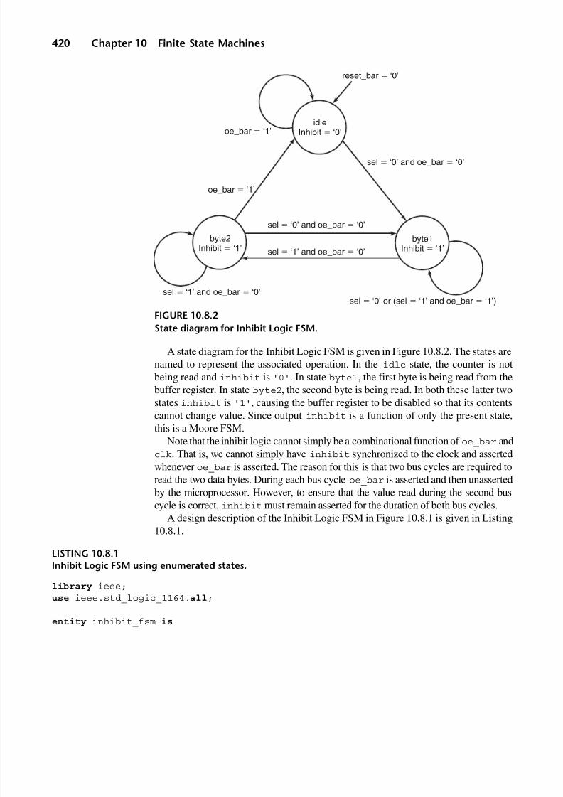
8/9/2019 VHDL for Engineers - Kenneth L. Short.pdf
http://slidepdf.com/reader/full/vhdl-for-engineers-kenneth-l-shortpdf 453/719
420 Chapter 10 Finite State Machines
A state diagram for the Inhibit Logic FSM is given in Figure 10.8.2. The states arenamed to represent the associated operation. In the idle state, the counter is notbeing read and inhibit is '0'. In state byte1, the first byte is being read from thebuffer register. In state byte2, the second byte is being read. In both these latter two
states inhibit is '1', causing the buffer register to be disabled so that its contentscannot change value. Since output inhibit is a function of only the present state,this is a Moore FSM.
Note that the inhibit logic cannot simply be a combinational function of oe_bar andclk. That is, we cannot simply have inhibit synchronized to the clock and assertedwhenever oe_bar is asserted. The reason for this is that two bus cycles are required toread the two data bytes. During each bus cycle oe_bar is asserted and then unassertedby the microprocessor. However, to ensure that the value read during the second buscycle is correct, inhibit must remain asserted for the duration of both bus cycles.
A design description of the Inhibit Logic FSM in Figure 10.8.1 is given in Listing10.8.1.
LISTING 10.8.1Inhibit Logic FSM using enumerated states.
library ieee;use ieee.std_logic_1164.all;
entity inhibit_fsm is
FIGURE 10.8.2
State diagram for Inhibit Logic FSM.
reset_bar ‘0’
idle
Inhibit ‘0’
byte2Inhibit ‘1’
byte1Inhibit ‘1’
sel ‘0’ or (sel ‘1’ and oe_bar ‘1’)
oe_bar
‘1’
oe_bar ‘1’
sel ‘1’ and oe_bar ‘0’
sel ‘0’ and oe_bar ‘0’
sel ‘0’ and oe_bar ‘0’
sel ‘1’ and oe_bar ‘0’

8/9/2019 VHDL for Engineers - Kenneth L. Short.pdf
http://slidepdf.com/reader/full/vhdl-for-engineers-kenneth-l-shortpdf 454/719
Section 10.8 Inhibit Logic FSM Example 421
port (rst_bar: in std_logic;clk: in std_logic;sel: in std_logic;inhibit : out std_logic;oe_bar: in std_logic);
end inhibit_fsm;
architecture behav of inhibit_fsm is
type inhib_state is (idle, byte1, byte2);signal present_state, next_state : inhib_state;
begin
inhib_sreg: process (clk)begin
if rising_edge(clk) thenif rst_bar = '0' then
present_state <= idle;else
present_state <= next_state;end if;
end if;end process;
inhib_output: process (present_state)begin
case present_state is
when byte1 | byte2 =>inhibit <= '1'; when others=>inhibit <= '0';
end case;end process;
inhib_nxt_state: process (present_state, sel, oe_bar)begin
case present_state is
when idle =>if sel = '0' and oe_bar = '0' then next_state <= byte1;else next_state <= idle;end if;
when byte1 =>if sel = '1' and oe_bar = '0' then next_state <= byte2;
(Cont.)

8/9/2019 VHDL for Engineers - Kenneth L. Short.pdf
http://slidepdf.com/reader/full/vhdl-for-engineers-kenneth-l-shortpdf 455/719
422 Chapter 10 Finite State Machines
LISTING 10.8.1 (Cont.)
else next_state <= byte1;end if;
when byte2 =>if oe_bar = '1' then next_state <= idle;elsif sel = '0' and oe_bar = '0' then next_state <= byte1;else next_state <= byte2;end if;
end case;end process;
end behav;
The Inhibit Logic FSM is partitioned into three processes: inhib_sreg,
inhib_output, and inhibit_nxt_state.The Inhibit Logic FSM uses enumerated states. A type is declared for the
enumerated states, and signals for the present state and next state are declared to beof this type:
type inhib_state is (idle, byte1, byte2);signal present_state, next_state : inhib_state;
At this point, the states are abstract, which is very convenient for functionalsimulation. The signals present_state and next_state can be displayed as partof the output waveforms of a functional simulation. These signals will be displayed
having the values idle, byte1, or byte2. This makes it convenient to verify that statetransitions occur in the correct order. However, before we can proceed with synthesis,we must either choose a state assignment ourselves or let the synthesizer choose.
10 .9 CO UN T ER S AS MO ORE F SM S
A simple counter is a special case of a Moore FSM where there are no inputs(other than the clock and reset) and the outputs are taken directly from the state
register. Figure 10.1.5 is modified to represent a simple counter as a Moore FSMin Figure 10.9.1. This is accomplished by eliminating the inputs and the combina-tional logic that computes the outputs.
2-bit BinaryCounter FSM
For example, consider a 2-bit binary counter described as a Moore FSM. If thecounter resets to 0, it can be represented by the state diagram in Figure 10.9.2.

8/9/2019 VHDL for Engineers - Kenneth L. Short.pdf
http://slidepdf.com/reader/full/vhdl-for-engineers-kenneth-l-shortpdf 456/719
Section 10.9 Counters as Moore FSMs 423
When the counter is reset, it is placed in its initial state and its outputs are 00. Ateach triggering clock edge, the counter transitions to its next state. Since there are noinputs and the outputs are taken directly from the state register, the directed arcs arenot labeled. As previously stated, an unlabeled arc indicates an unconditional
transition.Table 10.9.1 is the state table for the 2-bit counter. This table provides, in tabularform, the same information as the state diagram.
A description of the 2-bit counter as a Moore FSM is given in Listing 10.9.1.
FIGURE 10.9.1
A simple counter as a Moore FSM that requires no combinational output logic.
CombinationalNext StateLogic
S t a t e
R e g i s t e r
Outputs
next_statepresent_state
clock
FIGURE 10.9.2
State diagram for a 2-bit binary counter.
00
11
10
01

8/9/2019 VHDL for Engineers - Kenneth L. Short.pdf
http://slidepdf.com/reader/full/vhdl-for-engineers-kenneth-l-shortpdf 457/719
424 Chapter 10 Finite State Machines
LISTING 10.9.1Counter with state encoding defined by constants.
library ieee;use ieee.std_logic_1164.all;
entity cnt2bitc is
port (clk, reset: in std_logic;count: out std_logic_vector(1 downto 0));
end;
architecture behavior of cnt2bitc is
subtype state is std_logic_vector (1 downto 0);signal present_state, next_state : state;constant state0: state := "00";constant state1: state := "01";constant state2: state := "10";constant state3: state := "11";
begin
process (clk)begin
if rising_edge(clk) then
if ( reset='1' ) then
present_state <= state0;else
present_state <= next_state;end if;
end if;end process;
process (present_state)begin
case present_state is
when state0 =>next_state <= state1;
when state1 =>
Table 10.9.1State table for a 2-bit counter.
Present State Next State
00 01
01 1010 11
11 00
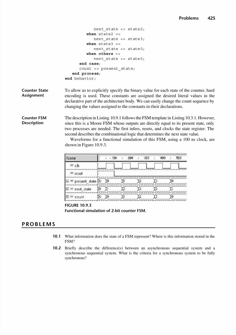
8/9/2019 VHDL for Engineers - Kenneth L. Short.pdf
http://slidepdf.com/reader/full/vhdl-for-engineers-kenneth-l-shortpdf 458/719
Problems 425
next_state <= state2; when state2 =>
next_state <= state3; when state3 =>
next_state <= state0; when others =>
next_state <= state0;end case;count <= present_state;
end process;end behavior;
Counter StateAssignment
To allow us to explicitly specify the binary value for each state of the counter, hardencoding is used. These constants are assigned the desired literal values in thedeclarative part of the architecture body. We can easily change the count sequence bychanging the values assigned to the constants in their declarations.
Counter FSMDescription
The description in Listing 10.9.1 follows the FSM template in Listing 10.3.1. However,since this is a Moore FSM whose outputs are directly equal to its present state, onlytwo processes are needed. The first infers, resets, and clocks the state register. Thesecond describes the combinational logic that determines the next state value.
Waveforms for a functional simulation of this FSM, using a 100 ns clock, areshown in Figure 10.9.3.
PROBLE MS
10.1 What information does the state of a FSM represent? Where is this information stored in theFSM?
10.2 Briefly describe the difference(s) between an asynchronous sequential system and asynchronous sequential system. What is the criteria for a synchronous system to be fullysynchronous?
FIGURE 10.9.3
Functional simulation of 2-bit counter FSM.

8/9/2019 VHDL for Engineers - Kenneth L. Short.pdf
http://slidepdf.com/reader/full/vhdl-for-engineers-kenneth-l-shortpdf 459/719
426 Chapter 10 Finite State Machines
10.3 What determines the minimum length of time a fully synchronous FSM remains in a state?How can such a FSM remain in the same state for a longer period of time?
10.4 Briefly describe the difference(s) between a Mealy and a Moore FSM.
10.5 Draw a state diagram for each of the following types of flip-flops. Also specify which areMealy FSMs and which are Moore FSMs.
(a) D flip-flop(b) S-R flip-flop(c) J-K flip-flop(d) T flip-flop
10.6 Draw a state diagram for a 2-bit right shift register, which is otherwise identical to the 4-bitshift register in Listing 9.2.1.
10.7 Draw a state diagram for a 3-bit counter, which is otherwise identical to the 12-bit counter inListing 9.4.4.
10.8 What is the operation of the FSM represented by the state diagram in Figure 10.2.1(a)? In otherwords, what does this FSM do? What is the operation of the FSM represented by the state
diagram in Figure 10.2.1(b)?10.9 Draw a state/output table for the FSMs in Figures 10.2.1(a) and 10.2.1(b).
10.10 What is the purpose of each of the three processes in a three-process template for a FSMdescription? Which of these processes are sequential and which are combinational? What isthe advantage of using the three-process approach to describing a FSM?
10.11 In which process of the three process template does the FSM’s reset appear? Under whatcondition would the reset signal’s name appear in this process’s sensitivity list?
10.12 Rewrite the process state_reg in the template in Listing 10.3.1 to implement anasynchronous reset.
10.13 Write a three-process description of the FSM represented by the state diagram in Figure 10.2.1(a).
10.14 Write a three-process description of the FSM represented by the state diagram in Figure 10.2.1(b).
10.15 Write a two-process description of the FSM represented by the state diagram in Figure 10.2.1(b).
10.16 Write a description for an alternative architecture for the BCD synchronous up/down counterin Problem 9.21. The entity declaration remains the same. Describe the BCD counter as a FSM.The state register is to be written as a process. The next state logic and the output logic are toeach be written as conditional signal assignment statements. Use an unsigned signal torepresent the count.
When considered as an FSM, is this a Mealy or Moore machine? Explain your reasoning.
10.17 A 2-bit sequencer (counter) produces the output sequence 00, 11, 10, 01, and then repeats. Thesequencer has a synchronous reset input,
reset_bar, which, when asserted, causes the
output to be 00.

8/9/2019 VHDL for Engineers - Kenneth L. Short.pdf
http://slidepdf.com/reader/full/vhdl-for-engineers-kenneth-l-shortpdf 460/719
Problems 427
(a) Draw a state diagram for the sequencer.(b) Write a complete design description of the sequencer. The description must consist of two
or three processes that form a FSM.(c) Is this FSM a Mealy or Moore FSM? Justify your answer.
10.18 Draw a state diagram, using a minimal number of states, to describe a Moore FSM implementa-
tion of the event detector in Problem 9.22. Write an architecture body that describes theevent_detector as a Moore FSM. The state register and next state logic are to be described usingprocesses. The output logic is to be described using a conditional signal assignment statement. If the input is a square wave, what is its maximum frequency relative to the system clock frequency,so that each input event is represented by a separate pulse at the system’s output? Explain yourreasoning.
10.19 A periodic waveform generator system is required that generates three outputs:w, x, and y. Thesystem has inputs clk and rst_bar. The output waveform repeats every 80 ns. One periodof the required output is represented by the following waveforms:
(a) Write a complete VHDL description of a FSM that implements the waveform generator.The description must follow the three-process template and use enumerated states. Thesystem is reset by the asynchronous reset signal rst_bar.
(b) Specify the state assignment that you would expect to lead to the simplest hardware.
Justify your answer.
10.20 A sequence recognizer generates a 1 output whenever it receives the input sequence 101.(a) Draw a state diagram for a Moore FSM implementation this sequence recognizer. Use as
few states as possible.(b) Write a complete description of a Moore FSM implementation of this sequence recognizer.
Use a three-process format with enumerated states and a synchronous reset.
10.21 A sequence recognizer generates a 1 output whenever it receives the input sequence 101.(a) Draw a state diagram for a Mealy FSM implementation of this sequence recognizer. Use
as few states as possible.(b) Write a complete description of a Mealy FSM implementation of this sequence recognizer.
The implementation must have a registered output. Use a three-process format withenumerated states and a synchronous reset.
W
X
Y

8/9/2019 VHDL for Engineers - Kenneth L. Short.pdf
http://slidepdf.com/reader/full/vhdl-for-engineers-kenneth-l-shortpdf 461/719
428 Chapter 10 Finite State Machines
10.22 A clocked synchronous system is described by the following state diagram:
(a) Write a design description of the synchronous system describing it as a FSM withenumerated states and following the three-process template given in this chapter. Use theentity declaration given below:
entity jkfsm isport(
j : in std_logic;k : in std_logic;
rst_bar : in std_logic;-- synchronous resetclk : in std_logic;q : out std_logic;q_bar : out std_logic);
end jkfsm;
(b) Is the machine as described by its state diagram a Mealy or Moore FSM? Explain youranswer.
10.23 A clocked synchronous sequence detector that detects the input sequence, or subsequence,1101 is to be designed. The sequence detector has a data input x and a data output y. The input
sequence is sampled on the rising edge of the sequence detector’s clock input, clk. When thelast 1 in a sequence 1101 is clocked in, output y should become and remain a 1 until the nexttriggering clock edge.(a) Draw a state diagram of a Mealy FSM with the minimum number of states that realizes the
sequence detector.(b) Write a complete two-process VHDL FSM design description of the sequence detector.
One process handles the state change and the other handles combinational functions. Writethis description in a fashion that allows the synthesizer to do the state assignment.
clear
q < ‘0’;
q_bar < ‘1’;
set
q < ‘1’;
q_bar < ‘0’;
@ELSE
rst_bar ‘0’
k ‘1’
j ‘1’
@ELSE

8/9/2019 VHDL for Engineers - Kenneth L. Short.pdf
http://slidepdf.com/reader/full/vhdl-for-engineers-kenneth-l-shortpdf 462/719
Problems 429
10.24 A programmable delay is created using a 10-bit counter, a 10-to-1 multiplexer, and a FSM. Ablock diagram of the system follows. The system is able to produce any one of 10 possibledelays based on the value of its select_counter_bit input. For each increase of theselect_counter_bit value by 1, the delay doubles.
The idea behind the design is that the select_counter_bit value selects one of the10 output bits of the 10-bit counter. When the start_delay input is asserted, theend_of_delay output becomes a 0 and the counter begins counting. When the selectedcounter bit changes from 0 to 1, the counter stops counting and end_of_delay becomes a 1.(a) Draw a state diagram for a Moore type FSM that implements the prog_delay_fsm
component of the block diagram. Use as few states in the diagram as possible.(b) Write a three-process description of the prog_delay_fsm entity.(c) Write an expression that specifies the length of time thatend_of_delay is a 0.
10.25 The state diagram in Figure 10.5.4 is for a Mealy FSM that implements a 4X decoder. Draw astate diagram for a Moore FSM that implements the same functionality.
10.26 What is a one-hot state assignment and what advantages does it have? With what type of PLDis a one-hot state assignment most likely to be advantageous and why?
10.27 What is the difference between a sequential and a Gray code state assignment? If a FSM haseight states, which of these two assignments will require the most bits in its state register?
10.28 Assuming two different state assignments require the same number of bits in their stateregisters, is it possible for the choice of assignments to have any impact on the logicsynthesized? Explain your answer.
10.29 If you are using explicit state encoding for a FSM, should you enable or disable the “FSMCompiler” feature in Synplify? Explain your answer.
10.30 Write a complete Moore FSM VHDL design description of a 3-bit Gray code counter. Thecounter has an active-low synchronous clear input (clr). The 3-bit Gray code count sequenceis 000, 001, 011, 010, 110, 111, 101, 100, and 000 (and then repeats).
10.31 A sequencer (counter) has a 3-bit output and is implemented as a FSM. The sequencer’s statesare constants named state_a, state_b, and so on. The sequencer starts in state_a andsequences through five unique states, returning to state_a. The state assignment is definedin the design description by the initial value assigned to each constant. Write the sequencerdesign description and assign initial values to the states so that the output sequences in binaryfrom “000” to “100” and then back to “000”.
10.32 A counter is used to generate a sequence of outputs that are control signals, thus implementinga controller. The control signals are directly encoded as the counter’s outputs. The control
prog_delay_fsm
u3
clk
rst_barstart_delay
counter_bit
clear_cntr
enable_cntrend_of_delay
mux_10to1
u2
[9:0]
inputs[9:0][3:0]
select_input[3:0] counter_bit
counter_10bit
u1
clk
rst_barclear_cntrenable_cntr
[9:0]
counter[9:0] end_of_delay
elect_counter_bit[3:0][3:0]
start_delay
rst_bar
clk

8/9/2019 VHDL for Engineers - Kenneth L. Short.pdf
http://slidepdf.com/reader/full/vhdl-for-engineers-kenneth-l-shortpdf 463/719
430 Chapter 10 Finite State Machines
signals are labeled A, B, C, and D. Their sequence of values is 0000, 0001, 0110, 1100, 1000and 0000 (sequence repeats).
(a) Write a complete VHDL design description of the controller as a FSM using either two orthree processes as is appropriate. The outputs are to be declared as scalars. The counter hasa synchronous reset that is active low.
(b) Is this controller a Mealy or Moore FSM? Explain your answer.10.33 A sequence recognizer has a single input and a single output. The output of the sequence
recognizer is a 1 if and only if the last four input values were 0101. The sequence recognizerhas a synchronous active low reset input.
(a) Draw a state diagram for the sequence recognizer.(b) Write a complete VHDL design description of the sequence recognizer as a two- or three-
(whichever is most appropriate) process FSM.

8/9/2019 VHDL for Engineers - Kenneth L. Short.pdf
http://slidepdf.com/reader/full/vhdl-for-engineers-kenneth-l-shortpdf 464/719
431
Chapter 11
ASM Charts and RTL Design
An alternative way to graphically represent a FSM is to use an algorithmic statemachine (ASM) chart. ASM charts are similar to traditional flow charts, except thatthey also contain implicit timing information in a manner similar to state diagrams.
All digital systems can be thought of as implementing algorithms. In a complexsystem, each task in an algorithm might be accomplished by a separate component.A task involves either the accomplishment of some action or a data manipulation. AFSM can be used to control when each component performs its task to accomplishthe algorithm.
A system that performs a data manipulation can be viewed as consisting of a datapath and a control. The data path consists of the components that manipulate andstore the data. The control consists of the component that sequences when specificmanipulations take place and when specific data is stored. The control is imple-mented by one or more FSMs. Design at this level of abstraction is called registertransfer level (RTL) design.
1 1. 1 A LG OR IT HM IC S TA TE M AC HI NE C HA RT S
Algorithms An algorithm is a finite sequence of steps for performing a task or solving a logical ormathematical problem. All digital systems can be viewed as implementing algorithms.In some systems, this view is obvious; for example, when a system implements acomputational algorithm. In others, the algorithmic nature of the system may not be asreadily apparent.
In the previous chapter we used state diagrams as a graphical way of conceptual-izing and representing FSMs. A state diagram is also a graphical way of representingan algorithm.
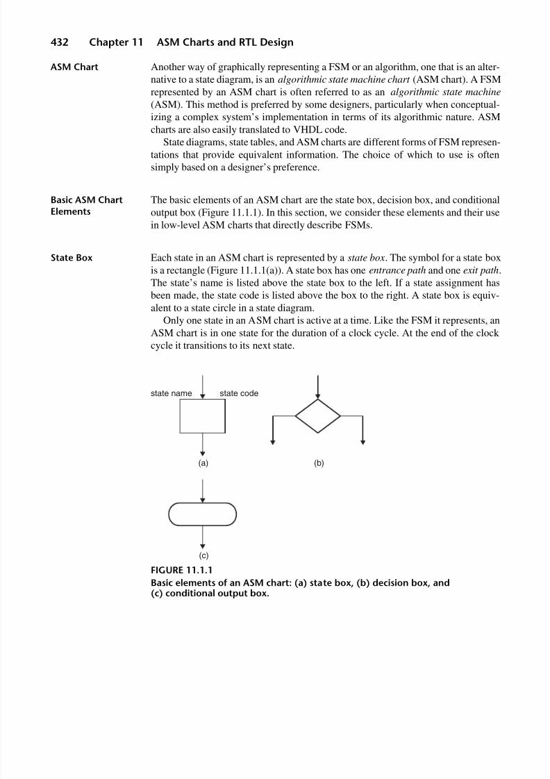
8/9/2019 VHDL for Engineers - Kenneth L. Short.pdf
http://slidepdf.com/reader/full/vhdl-for-engineers-kenneth-l-shortpdf 465/719
432 Chapter 11 ASM Charts and RTL Design
ASM Chart Another way of graphically representing a FSM or an algorithm, one that is an alter-native to a state diagram, is an algorithmic state machine chart (ASM chart). A FSMrepresented by an ASM chart is often referred to as an algorithmic state machine
(ASM). This method is preferred by some designers, particularly when conceptual-izing a complex system’s implementation in terms of its algorithmic nature. ASM
charts are also easily translated to VHDL code.State diagrams, state tables, and ASM charts are different forms of FSM represen-
tations that provide equivalent information. The choice of which to use is oftensimply based on a designer’s preference.
Basic ASM ChartElements
The basic elements of an ASM chart are the state box, decision box, and conditionaloutput box (Figure 11.1.1). In this section, we consider these elements and their usein low-level ASM charts that directly describe FSMs.
State Box Each state in an ASM chart is represented by a state box . The symbol for a state boxis a rectangle (Figure 11.1.1(a)). A state box has one entrance path and one exit path.The state’s name is listed above the state box to the left. If a state assignment hasbeen made, the state code is listed above the box to the right. A state box is equiv-alent to a state circle in a state diagram.
Only one state in an ASM chart is active at a time. Like the FSM it represents, anASM chart is in one state for the duration of a clock cycle. At the end of the clock cycle it transitions to its next state.
FIGURE 11.1.1
Basic elements of an ASM chart: (a) state box, (b) decision box, and(c) conditional output box.
state name state code
(a) (b)
(c)

8/9/2019 VHDL for Engineers - Kenneth L. Short.pdf
http://slidepdf.com/reader/full/vhdl-for-engineers-kenneth-l-shortpdf 466/719
Section 11.1 Algorithmic State Machine Charts 433
Inside a state box are listed signal assignments that are made unconditionallywhile in that state. These are assignments that depend only on the state of the FSM(Moore assignments).
Immediate
Assignments
Assignments made in a state box can be either immediate or delayed. An immediate
assignment takes effect immediately upon entering the state.Most low-level ASM charts deal with only binary-valued signals. For
conciseness, only assignments that assert a signal are listed in a state box. Theasserted signal’s name is written in the state box without writing an assignmentsymbol and value. If a signal’s name does not appear in a state box, it is assumed thatthe signal is assigned its unasserted value in that state.
Alternatively, if a style of ASM chart is used where an assignment symbol is usedto represent an immediate assignment, then an equal sign (=) is used and theassigned value is specified.
DelayedAssignments
A delayed assignment does not take effect until the state following the one in whichthe assignment is made. On a low-level ASM chart, we simply write in the state boxthe name of the signal that is asserted to cause the delayed assignment to occur. Forexample, consider a counter whose output is named count and that has an enableinput named en_count. If the value of count is to be incremented in a particularstate, then en_count appears in that state box. This means that en_count isimmediately asserted in that state. At the next triggering clock edge, count is incre-mented. Therefore, the newly incremented value of count is not available until thenext state time.
ASM charts can be used to represent systems at different levels of abstraction. An
ASM chart representing an algorithm at a high level of abstraction may use anassignment symbol to represent a delayed assignment. Either a left or a rightpointing arrow ( ← ) or ( → ) is used. This assignment symbol is called the delay
operator . For example, if the counter is to be incremented in a particular state, wecould write in the state box:
count ← count + 1
The new counter value (count + 1) is computed in the current state, but thecounter is not loaded with this new value until the next triggering clock edge. So, thenew count value is not available at the counter’s output until the next state. This is anabstract representation of the operation to be performed on the counter and would
likely be used in an ASM chart representing an algorithm at a high level of abstraction. Later, in a lower-level ASM chart, this operation is represented bywriting only the name of the counter’s enable input in the state box.
Note that signals assigned a value with a delay operator are not limited to scalarsignals and could be vectors. In addition, signals assigned a value using the delayoperator keep their previous values until a new value is assigned.

8/9/2019 VHDL for Engineers - Kenneth L. Short.pdf
http://slidepdf.com/reader/full/vhdl-for-engineers-kenneth-l-shortpdf 467/719
434 Chapter 11 ASM Charts and RTL Design
Decision Box A decision box (or condition box) is a diamond-shaped box (Figure 11.1.1(b)) thatcontains a conditional expression involving the FSM’s inputs. This condition deter-mines the exit path to the next state. A decision box is used in conjunction with aconditional output box to determine the conditions under which Mealy outputassignments are made.
A decision box has one entrance path and two exit paths. One path is taken whenthe condition is true and the other path is taken when it is false. Exit paths are usuallylabeled 1 and 0 or T and F, for true and false, respectively.
ConditionalOutput Box
A conditional output box specifies assignments that are made when all the condi-tions in the decision boxes that provide the path from a state box to the conditionaloutput box are true. These are Mealy assignments. An output specified in a condi-tional output box can change value during the state time, if the inputs in the decisionboxes leading to the conditional output box change value. A conditional output boxhas rounded corners (Figure 11.1.1(c)) to differentiate it from a state box. It has one
entrance path and one exit path.
ASM Block An ASM block consists of one state box and the tree of decision boxes and condi-tional output boxes that may optionally emanate from that state box up to, but notincluding, the state boxes that terminate the tree. An ASM block has one entrancepath and one or more exit paths.
Each ASM block describes operations executed in a single state. As previouslystated, the state box represents the state just as a circle does on a state diagram. Thedecision boxes and conditional output boxes represent the state transitions andMealy outputs that are represented by labeled directed arcs in a state diagram.
Decision boxes and conditional output boxes belong to a single state box andcannot be shared by other state boxes.The operations specified in the state box and all decision boxes and conditional
output boxes in an ASM block execute concurrently while in that state.
ASM Block Example A simple example of an ASM block is given in Figure 11.1.2. The portion of theASM chart that represents the single ASM block s2 is enclosed by a dashedrectangle. This ASM block has one entrance path and three exit paths. The staterepresented by this ASM block is state s2. State boxes s3, s4, and s5 are not part of this ASM block. Output v is unconditionally asserted in state s2. Thus, v is a Moore
output. Output w is asserted only if input a is asserted. Output x is asserted only if inputs a and b are both asserted. Outputs w and x are Mealy outputs.
Parallel versusSeries DecisionBoxes in an ASMBlock
Two equivalent ASM blocks are shown in Figure 11.1.3. These ASM blocks areequivalent, because of the property that all operations within an ASM block areperformed concurrently, not sequentially.

8/9/2019 VHDL for Engineers - Kenneth L. Short.pdf
http://slidepdf.com/reader/full/vhdl-for-engineers-kenneth-l-shortpdf 468/719
Section 11.1 Algorithmic State Machine Charts 435
FIGURE 11.1.2
An ASM block.
FIGURE 11.1.3
Equivalent ASM blocks.
1
0
1
0
a
b
w
x
s2
s3 s4 s5
v
1
0
1
0
1
0
a
b
c
w
x
y
s0
1
0
b
x
s0
1
0
a
w
1
0
c
y

8/9/2019 VHDL for Engineers - Kenneth L. Short.pdf
http://slidepdf.com/reader/full/vhdl-for-engineers-kenneth-l-shortpdf 469/719
436 Chapter 11 ASM Charts and RTL Design
In each case the ASM block indicates that, in state s0, w is asserted only if a is 1,x is asserted only if b is 1, and y is asserted only if c is 1. While the series represen-tation is often preferred, they are equally valid.
General Rules
for Constructingan ASM Chart
An ASM chart consists of one or more interconnected ASM blocks. For an ASM
chart to be well defined, there must be a unique next state for each state and set of conditions. And, each exit path from an ASM block must connect to a state box.
A decision box in an ASM block must follow and be associated with a state box.A conditional output box must follow a decision box.
Moore FSM PositiveEdge Detector ASMChart
An ASM chart for the Moore FSM positive edge detector, equivalent to the statediagram in Figure 10.4.1, is given in Figure 11.1.4.
FIGURE 11.1.4
ASM chart for Moore FSM positive edge detector.
a
state_a
state_b
a
a_pe
state_c
a
1
0
1
0
1
0

8/9/2019 VHDL for Engineers - Kenneth L. Short.pdf
http://slidepdf.com/reader/full/vhdl-for-engineers-kenneth-l-shortpdf 470/719
Section 11.1 Algorithmic State Machine Charts 437
There are three ASM blocks in this chart. Note that, in an ASM chart, the ASMblocks are usually not delineated by dashed lines, as was done for conceptualpurposes in Figure 11.1.2. Each ASM block in Figure 11.1.4 consists of a state boxand a single decision box. For example, the state box for state_a is followed by adecision box that determines, based on the value of a, whether the next state
transition is back to state_a or is to state_b. The conditional expression in thedecision box is simply the input name, a. This expression is equivalent to a = 1.
Output a_pe is asserted only in state state_c. The assertion of a_pe isindicated by simply writing the name a_pe in the state box state_c. This meansa_pe is asserted in this state. Since a_pe is asserted high, this is equivalent towriting a_pe = 1 in state box state_c. The other states do not list a_pe, so a_pe isnot asserted in those states. This is equivalent to writing a_pe = 0 in state boxesstate_a and state_b.
With this shorthand notation in mind, the correspondence between this ASM statechart and the state diagram in Figure 10.4.1. is clear.
Mealy FSM PositiveEdge Detector ASMChart
An ASM chart for the Mealy FSM positive edge detector, equivalent to the statediagram in Figure 10.4.4, is given in Figure 11.1.5.
There are two ASM blocks in this chart. The first consists of the state box forstate_a and a decision box. The second consists of a state box for state_b, adecision box, and a conditional output box.
In ASM block state_b, output a_pe is listed in a conditional output box. Sincethe path to the conditional output box is through the decision box’s exit path corre-sponding to a being asserted, the assertion of a_pe is conditioned on a being 1. Thisassignment is conditional and immediate.
The correspondence between this ASM chart and the state diagram in Figure10.4.4 is also clear.
ASM Charts versusState Diagrams
While state diagrams and ASM charts are equivalent, there are some practical differ-ences that may make one or the other preferable.
A state diagram is usually drawn to represent a completely specified FSM. Thus,for every state, a next state transition is shown for each possible input combination. Inaddition, the value of every output is indicated for each possible input condition whilein that state. The resulting extensive labeling of arcs for Mealy outputs and outputvalues inside, or associated with, state symbols for Moore outputs can make statediagrams for practical FSMs difficult to interpret. This extensive labeling also implies
that in each state each input and each output is equally important to the understandingof the operation of the FSM. For a practical FSM, this is usually not the case.
Clearly, state diagrams can be simplified by following certain conventions likenot labeling transitions back to the same state in Moore machines, as was done insome examples in the previous chapter.
The state boxes in ASM charts only list the outputs that are asserted in each state.These are the outputs that are important when in that state. The decision boxes in an

8/9/2019 VHDL for Engineers - Kenneth L. Short.pdf
http://slidepdf.com/reader/full/vhdl-for-engineers-kenneth-l-shortpdf 471/719
438 Chapter 11 ASM Charts and RTL Design
ASM block only list the inputs that are important in determining the next state transi-tions and the conditional outputs when in that state. These are the inputs that areimportant in that state. This simplification often makes it easier to interpret theoperation of an FSM represented by an ASM chart.
1 1. 2 C ON VE RT IN G A SM CH AR TS TO VH DL
If the three-process FSM template in Listing 10.3.1 is followed, writing a VHDL
description of a FSM from an ASM chart is straightforward. The state register andnext state processes are written in exactly the same fashion as before for statediagrams. For the output process, some additional interpretation is required to writethe VHDL code from the ASM chart.
For the next state process, the contents of the case statement’s when branches aredetermined directly from the ASM blocks. For example, Figure 11.2.1 shows theASM chart for the Mealy positive edge detector. The middle column in the figure
FIGURE 11.1.5
ASM chart for Mealy FSM positive edge detector.
a
state_a
state_b
a
1
1
0
0
a_pe

8/9/2019 VHDL for Engineers - Kenneth L. Short.pdf
http://slidepdf.com/reader/full/vhdl-for-engineers-kenneth-l-shortpdf 472/719
Section 11.2 Converting ASM Charts to VHDL 439
gives the when branches of the case statement in the next state process. Each whenbranch is associated with the ASM block to its left.
Missing OutputAssignments inASM Charts
Since the output and next state processes in the three-process FSM template describecombinational logic, each time one of these processes executes, each of its outputsmust be assigned a value.
For the output process, only assignments that assert outputs are listed in the ASMchart. This means that, when writing code for a when branch that corresponds to anASM block where no assignment to an output is indicated, the appropriate assignmentmust be added.
FIGURE 11.2.1
VHDL when branch code corresponding to ASM blocks for Mealy FSM positiveedge detector.
ASM Chart Code in next state process casestatement
Code in output processcase statement
when state_a =>if a = '0' then
next_state <= state_b;else
next_state <= state_a;end if;
when state_a =>a_pe <= '0';
when state_b =>if a = '1' then
next_state <= state_a;else
next_state <= state_b;end if;
when state_b =>if a = '1' then
a_pe <= '1';else
a_pe = '0';end if;
a
state_a
state_b
a
1
1
0
0
a_pe

8/9/2019 VHDL for Engineers - Kenneth L. Short.pdf
http://slidepdf.com/reader/full/vhdl-for-engineers-kenneth-l-shortpdf 473/719
440 Chapter 11 ASM Charts and RTL Design
For example, in the ASM block for state_a in Figure 11.2.1, there is noassignment to a_pe listed. Accordingly, a_pe is not asserted in that state and mustbe assigned '0'. In the rightmost column, the when branch for state_a includesthis assignment.
In state_b, when a = '1', the conditional output box indicates that a_pe is
asserted. Accordingly, a_pe is assigned a '1' by the if statement in the when branchcorresponding to the ASM block for state_b, in the rightmost column in Figure11.2.1.
In state_b, when a = '0', no conditional assignment to a_pe is listed. Accord-ingly, a_pe is assumed to be unasserted for this condition. The if statement in therightmost column requires an else branch that assigns a_pe a '0', since that is itsunasserted value. Note that we want to assign a value to a_pe equal to its unassertedvalue. We do not want to remember the value of a_pe, which would be the result if we left out the else branch.
When the code for the when branches is placed in the case statements of theappropriate processes and the state register process is added, the description iscomplete. The resulting VHDL code is the same as in Listing 10.4.3.
A Simpler OutputProcess
When writing VHDL code for a FSM directly from an ASM chart, there is a simplerapproach that can be used for the output process. Since the ASM chart only indicateswhen a signal is asserted, we can simplify writing the code from the chart byincluding statements at the beginning of the output process to assign all outputs theirunasserted values.
These default assignment statements are followed by the case statement. Thewhen branches of the case statement then only contain assignments to the outputs
that are to be asserted. If the assertion of an output is conditional (Mealy output), theassignment statement is contained in an appropriate if statement. Code following thesimpler form of output process is given in Listing 11.2.1.
LISTING 11.2.1Simplified output process for positive edge detector written directlyfrom ASM chart.
outputs: process (present_state, a)begin
a_pe <= '0'; -- default unasserted value
case present_state is
when state_a =>null;
when state_b =>if a = '1' then
a_pe <= '1';

8/9/2019 VHDL for Engineers - Kenneth L. Short.pdf
http://slidepdf.com/reader/full/vhdl-for-engineers-kenneth-l-shortpdf 474/719
Section 11.3 System Architecture 441
end if;end case;
end process;
Using Concurrent
Statements for FSMOutputs
It is sometimes simpler to replace the output process with conditional signal assignment
statements. The ASM chart can be examined and a statement written to assign theasserted value to an output for all the conditions where such an assignment is warrantedand default to the unasserted value for all other conditions.
For example, from examination of the ASM chart in Figure 11.2.1, we couldwrite the conditional signal assignment statement:
a_pe <= '1' when present_state = state_b and a = '1'else '0':
This single statement replaces the output process in Listing 10.4.3.
11 .3 SY ST EM A RC H IT EC T UR E
In previous chapters we have considered the design of combinational systems andsimple sequential systems. We have also considered the FSM approach to designingsequential systems.
In theory, any synchronous sequential system can be implemented as a singleFSM. However, for a complex system with many inputs, outputs, and states, imple-mentation as a single FSM is impractical. It is preferable to decompose such asystem into simpler components.
Once the operation of a system has been specified in terms of an algorithm, thetasks that must be accomplished to perform the algorithm are known. For each task one or more well-defined components and their interconnection to accomplish thetask are determined. Each task must be performed at the appropriate time, as deter-mined by the algorithm, to accomplish the system’s overall task. In effect, the systemis decomposed into functional units (combinational and sequential components) thatimplement tasks, and one or more FSMs that control when each task is performed.
The interconnection of functional units and FSMs comprises the architecture of the complex system. Conceptually, two common architectural approaches for acomplex sequential system are: functional units and control, and data path and
control.These architectures are conceptually represented in Figure 11.3.1 for an algorithmthat consists of tasks A, B, and C. In both architectures, the control part of the systemis implemented by one or more FSMs.
Figure 11.3.1(a) represents an architecture where each functional unit is enabledby the control unit to carry out a particular task. When a functional unit completes itstask, it signals the control unit via a status signal. The control unit sequences theoperation of the functional units in the appropriate order, to achieve the overall

8/9/2019 VHDL for Engineers - Kenneth L. Short.pdf
http://slidepdf.com/reader/full/vhdl-for-engineers-kenneth-l-shortpdf 475/719
442 Chapter 11 ASM Charts and RTL Design
system function. In a simple system the tasks may be executed in sequence. Alterna-
tively, multiple functional units may be active at one time or a single functional unitmay be active repeatedly.
Figure 11.3.1(b) represents an architecture where there is a data path and control.The system is decomposed into a collection of functional units through which dataflows (a data path). Each functional unit consists of combinational logic and a register.The control enables each functional unit to carry out a particular task (data manipu-lation) on the data as it passes along the data path. The sequence of data manipulationsperformed accomplishes the desired overall transformation of data. The data outputfrom the data path is the computed result.
The main distinction between these two approaches is whether the system isviewed primarily as carrying out a sequence of actions or a sequence of data manip-ulations. In both approaches the functional units are accomplishing the tasks and thecontrol unit (FSM) is sequencing task execution to perform the algorithm.
Register TransferLevel (RTL) Design
The methodology used to design the architecture in Figure 11.3.1(b) is calledregister transfer level (RTL) design. The data path stores, routes, and processes data. Its
FIGURE 11.3.1
Common architectures: (a) functional units and control, (b) data path andcontrol.
Task A
control status
ext.inputs
ext.outputs
externalcontrol
Task B
control status
ext.inputs
ext.outputs
Task C
control status
ext.inputs
ext.outputs
externalstatus
FSM
(a)
Task A
control status
externalcontrol
Task B
control status
Task C
control status
externalstatus
FSM
(b)
externaldatainput
externalstatusoutput
data data
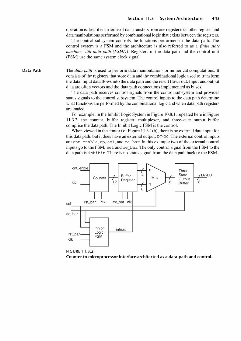
8/9/2019 VHDL for Engineers - Kenneth L. Short.pdf
http://slidepdf.com/reader/full/vhdl-for-engineers-kenneth-l-shortpdf 476/719
Section 11.3 System Architecture 443
operation is described in terms of data transfers from one register to another register anddata manipulations performed by combinational logic that exists between the registers.
The control subsystem controls the functions performed in the data path. Thecontrol system is a FSM and the architecture is also referred to as a finite state
machine with data path (FSMD). Registers in the data path and the control unit
(FSM) use the same system clock signal.
Data Path The data path is used to perform data manipulations or numerical computations. Itconsists of the registers that store data and the combinational logic used to transformthe data. Input data flows into the data path and the result flows out. Input and outputdata are often vectors and the data path connections implemented as buses.
The data path receives control signals from the control subsystem and providesstatus signals to the control subsystem. The control inputs to the data path determinewhat functions are performed by the combinational logic and when data path registersare loaded.
For example, in the Inhibit Logic System in Figure 10.8.1, repeated here in Figure11.3.2, the counter, buffer register, multiplexer, and three-state output buffercomprise the data path. The Inhibit Logic FSM is the control.
When viewed in the context of Figure 11.3.1(b), there is no external data input forthis data path, but it does have an external output, D7-D0. The external control inputsare cnt_enable, up, sel, and oe_bar. In this example two of the external controlinputs go to the FSM, sel and oe_bar. The only control signal from the FSM to thedata path is inhibit. There is no status signal from the data path back to the FSM.
FIGURE 11.3.2
Counter to microprocessor interface architected as a data path and control.
CounterBufferRegister
MuxThree-StateOutputBuffer
InhibitLogicFSM
cnt_enble
up
D7-D0
clk rst_bar clkrst_bar
clk
rst_bar
sel
oe_bar
inhibit
12
4
8
8 8
0
1

8/9/2019 VHDL for Engineers - Kenneth L. Short.pdf
http://slidepdf.com/reader/full/vhdl-for-engineers-kenneth-l-shortpdf 477/719
444 Chapter 11 ASM Charts and RTL Design
Generic View of aData Path
A more generic view of a data path represents it as a sequence of simple storageregisters separated by combinational logic (Figure 11.3.3). This view is particularlyappropriate for a pipelined data path.
CombinationalLogic “Cloud”
As shown in Figure 11.3.3, the combinational logic between registers is oftenconceptually represented by a “cloud” symbol. Each combinational logic “cloud”either transforms or routes the output of the storage register to its left and providesthe transformed or routed value as input to the storage register on its right. Often, asimple storage register and the combinational logic associated with it combine toproduce an operational register such as a shift register, counter, or arithmetic andlogic unit (ALU). Alternatively, the combinational logic might provide data routingbetween registers, such as demultiplexing or multiplexing.
Data in registers represent variables manipulated by the data path. The combina-tional logic in the data path manipulates the input data stream, as specified by controlinputs from the control subsystem. Outputs of registers become valid after atriggering clock edge. Register outputs are transformed by the combinational logic
during the time between triggering clock edges. Results computed by the combina-tional logic are stored in a register at the next triggering clock edge.
Control The control subsystem produces control signals based on its external inputs, statusinputs from the data path, and its present state. Control signals direct data routing in thedata path by selecting multiplexer and demultiplexer channels and enabling or disablingregisters. In addition to their clock inputs, registers typically have one or more enableinputs that are controlled to determine whether or not a register stores its input data atthe next triggering clock edge. Combinational logic blocks may also have controlinputs that determine what function they perform at any given time. For example, the
select inputs to demultiplexers and multiplexers are controlled to route data.
Control Word The values of all the control inputs to the data path are sometimes aggregated to forma control word. The bits of the control word determine the source and destinationregisters for data transfers and the operations performed in the data path during eachclock cycle. To cause the data path to accomplish its algorithm on the input data, thecontrol word must have the appropriate value for each clock cycle.
FIGURE 11.3.3
The cloud representation of a data path.
D Q QD D Q

8/9/2019 VHDL for Engineers - Kenneth L. Short.pdf
http://slidepdf.com/reader/full/vhdl-for-engineers-kenneth-l-shortpdf 478/719
Section 11.4 Successive Approximation Register Design Example 445
Scheduling The sequence of control words from the FSM is said to schedule the use of theresources (registers and combinational logic) in the data path.
1 1. 4 S UC CE SS IV E A PP RO XI MA TI ON R EG IS TE R
D E S I G N E X A M P L E
As an example of the partition of a system into a data path and control, this sectiondescribes the design of a successive approximation register (SAR). A SAR is an opera-tional register that is a component of a successive approximation analog-to-digitalconverter.
Analog-to-DigitalConverter
An analog-to-digital converter (ADC) converts its analog input voltage to a digitaloutput. An ADC’s analog input range is constrained and only voltages within its
range can be converted. For example, an ADC might have a 0 to 2.5V input range.Accordingly, the full-scale (FS) value of this input range is 2.5 V.
ADC Output as aBinary Fraction
An n-bit binary ADC produces an n-bit binary output that is proportional to itsanalog input voltage. The n-bit output is a binary fraction that represents the analoginput voltage as a fraction of the ADC’s FS input value. The binary point is assumedto be to the left of the most significant bit of the output. For example, if its inputvoltage is 1.875 V, a 4-bit ADC with a 0 to 2.5 V input range would produce anoutput of 1100. This output represents the binary fraction 0.1100 or 12/16 (75%) of FS. Thus, from the binary output, the analog input voltage can be computed to be0.75 × 2.5 V = 1.875 V.
SuccessiveApproximationADC
One popular type of ADC is a successive approximation ADC. It performs aconversion by generating a sequence of approximations that ultimately converge to thefinal binary output. A successive approximation ADC is constructed using a SAR, adigital-to-analog converter (DAC), and an analog comparator (Figure 11.4.1).
SAR Operation The purpose of the SAR is to generate the sequence of approximations that areoutput to the DAC during a conversion. At power on, the SAR’s reset_bar input isasserted for a short time, putting the SAR in its initial state.
When a conversion is desired, the SAR’s start of conversion (soc) input isasserted. The SAR then executes its successive approximation algorithm todetermine the binary result. During execution of this algorithm, the SAR uses thelogic value at its comp_in input to determine the next approximation value to outputto the DAC. When the conversion is complete, the end of conversion (eoc) statusoutput is asserted and the last approximation is the binary result. This value isavailable at output result.

8/9/2019 VHDL for Engineers - Kenneth L. Short.pdf
http://slidepdf.com/reader/full/vhdl-for-engineers-kenneth-l-shortpdf 479/719
446 Chapter 11 ASM Charts and RTL Design
SuccessiveApproximationAlgorithm
The successive approximation algorithm is illustrated in Figure 11.4.2. This flowchartimplies that the content of a single register is being manipulated, bit by bit, to producethe result.
The algorithm is a binary search that requires one iteration (clock cycle) todetermine each bit of the result. During each iteration, an approximation to the finalvalue is used as input to the DAC to generate an analog voltage (Figure 11.4.1). Theanalog comparator compares the DAC’s analog output voltage with the analog inputvoltage being converted.
During the first iteration, the most significant bit of the approximation is a 1 andall of its other bits are 0s. This approximation value is output to the DAC todetermine the value of the most significant bit of the result.
If the DAC analog output voltage produced by this approximation is less than orequal to the input analog voltage, the comparator output is a 1. In this case, the mostsignificant bit in the final result must be a 1, and is, therefore, left a 1 in the approxi-mation.
If, instead, the DAC voltage produced by the first approximation is greater thanthe input analog voltage, the comparator output is a 0. In this case, the most signif-icant bit in the final result must be a 0, and this bit is changed to a 0 in the approxi-mation.
To determine the next bit in the result, the corresponding bit in the approximation ismade a 1, with all other more significant bits of the approximation keeping their previ-ously determined values. The output of the comparator is used to determine whetherthe bit currently being determined must be a 1 in the final result and, therefore, must beleft a 1 in the approximation, or whether it must be changed back to 0. The stepsdescribed in this paragraph are repeated for each bit until the least significant bit hasbeen determined, completing the conversion.
FIGURE 11.4.1
Successive approximation ADC block diagram.
soc
clk
result
analog input
SAR
DAC
digital in
analog out
analogcomparator
eoc
comp _in
8
8
DAC analog output
reset_bar

8/9/2019 VHDL for Engineers - Kenneth L. Short.pdf
http://slidepdf.com/reader/full/vhdl-for-engineers-kenneth-l-shortpdf 480/719
Section 11.4 Successive Approximation Register Design Example 447
Figure 11.4.3 shows the sequence of approximations created by a 4-bit successive
approximation ADC with a range of 0 to 2.5 V and an input voltage of 1.875 duringa conversion. The figure shows the approximations output during the four iterationsrequired for the conversion. The fifth interval shows the final result at the end of theconversion.
VHDLRepresentationof SAR Algorithm
The successive approximation algorithm represented in Figure 11.4.2 could, alterna-tively, have been described directly in VHDL, as shown in Listing 11.4.1, for an 8-bitconversion.
This behavioral description is not synthesizable because the synthesizer requiresall of the wait statements in a process to be identical. However, it is a concise and
unambiguous way to describe the algorithm to someone who knows VHDL.
RTL Design of SAR The RTL design of the SAR involves creating a hardware architecture to implement thesuccessive approximation algorithm. When creating such an architecture, it may be thata direct one-to-one mapping of the algorithm to hardware is not conceptually thesimplest approach. For example, in the architecture to be described, two registers areactually used, rather than the single register implied in Figure 11.4.2 and Listing 11.4.1.
FIGURE 11.4.2
Flowchart of the successive approximation algorithm.
enter
set msb of
approx, clearall other bits
cmp 11
done?
exit
clear bit beingtested inapprox
set next bit tobe tested in
approx
yes
yes
no
no

8/9/2019 VHDL for Engineers - Kenneth L. Short.pdf
http://slidepdf.com/reader/full/vhdl-for-engineers-kenneth-l-shortpdf 481/719
448 Chapter 11 ASM Charts and RTL Design
LISTING 11.4.1Nonsynthesizable process describing successive approximation algorithm.
sac_alg : process
variable approx : std_logic_vector(7 downto 0);
begin wait until soc = '1'; -- wait to start conversioneoc <= '0'; -- unassert eoc approx := (others => '0'); -- generate approximationsfor i in 7 downto 0 loop
approx(i) := '1';result <= approx; -- output approximation wait until clk = '1'; wait for tpda; -- DAC and comparator progation delay if comp_in = '0' then -- read comparator and clear bit if necessary
approx(i) := '0';
elseapprox(i) := '1';
end if;end loop;result <= approx; -- output resulteoc <= '1'; -- assert eoc wait until clk = '1';
end process;
FIGURE 11.4.3
Approximations for a 4-bit conversion of an input voltage of 1.875 V by a 0 to2.5 V ADC.
0.5
1.0
1.5
2.0
2.5
0.0
1.875
inputvoltage
DACoutput
1000 1100 1110 1101 1100
DAC input and final result

8/9/2019 VHDL for Engineers - Kenneth L. Short.pdf
http://slidepdf.com/reader/full/vhdl-for-engineers-kenneth-l-shortpdf 482/719
Section 11.4 Successive Approximation Register Design Example 449
SAR RTLArchitecture
In our two-register approach, register approx_reg is used to hold the value of theprevious approximation during each iteration of the conversion and to hold the finalresult at the end of the conversion.
Another register, shftreg, holds a single 1 in the position of the bit of the resultbeing determined during a particular iteration of the algorithm. This 1 is shifted right
one bit position after each bit of the result is determined.The logical OR of the contents of these two registers provides the current approx-
imation to the DAC’s inputs.A RTL block diagram of the SAR is given in Figure 11.4.4. It shows the four
components that comprise the system: two registers, an OR gate, and a FSM. Thisdiagram is for an 8-bit conversion, but the design is easily scaled to any number of bits.
Componentapprox_reg
Component approx_reg is an 8-bit register that is cleared when reset. If its loadinput is asserted, approx_reg loads "00000000" at the next triggering clock edge.If its load input is not asserted and both its enable inputs, en1 and en2, are simulta-
neously asserted, approx_reg stores its 8-bit input data at the next triggering clock edge.
Componentshiftreg
Component shiftreg is an 8-bit right shift register that is cleared when reset. If itsload input is asserted, shiftreg loads "10000000" at the next triggering clock edge. If its load input is not asserted and its enable input en is asserted, shiftregshifts its contents to the right at the next triggering clock edge.
Componentor_function
The outputs of approx_reg and shiftreg are bitwise ORed by componentor_function. It is the output of or_function that is the current approximationvalue during the conversion and the final result when the conversion is complete.
SAR Data Path When viewed in terms of a data path and a control, the SAR’s data path consists of approx_reg, shft_reg, and or_function. This data path has no external datainputs. The output of or_function is the data path’s output. Control inputs to the datapath are the external input comp_in and outputs from the control FSM to en, en2, andload. The status output from the data path to the control FSM is last_bit_sig
(result(0)).
SAR Control Control saadc_fsm is a Moore FSM. To start a conversion, its external control inputsoc must be asserted. In response, saadc_fsm asserts the load inputs of bothregisters. At the next triggering clock edge component, approx_reg is loaded with"00000000" and shiftreg is loaded with "10000000". The OR of these tworegister’s outputs is the first approximation, "10000000".
Output result from the SAR is input to the DAC (Figure 11.4.1). The DACproduces an analog output voltage proportional to its binary input value. The analog

8/9/2019 VHDL for Engineers - Kenneth L. Short.pdf
http://slidepdf.com/reader/full/vhdl-for-engineers-kenneth-l-shortpdf 483/719
4 5 0
C h a p t e
r 1 1
A S M C h ar t s an d R T L D e s i gn
FIGURE 11.4.4
Block diagram of SAR.
saadc_fsm
u3
clk
reset_bar
soc[0]
last_bit
load
en
en2
eoc
or_function
u2
[7:0]a[7:0]
[7:0]b[7:0]
[7:0] [7:0]or_out[7:0]
approx_reg
u1
reset_bar
load
en1
en2clk
[7:0]d[7:0]
[7:0]qar[7:0]
shiftreg
u0
clr_bar
load
en
clk
[7:0]qout[7:0]
result[7:0]
eoc
clk
comp_in
soc
reset_bar
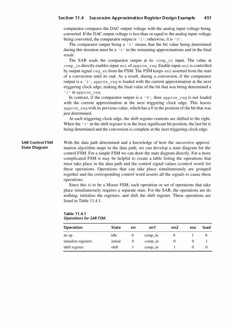
8/9/2019 VHDL for Engineers - Kenneth L. Short.pdf
http://slidepdf.com/reader/full/vhdl-for-engineers-kenneth-l-shortpdf 484/719
Section 11.4 Successive Approximation Register Design Example 451
comparator compares the DAC output voltage with the analog input voltage beingconverted. If the DAC output voltage is less than or equal to the analog input voltagebeing converted, the comparator output is '1'; otherwise, it is '0'.
The comparator output being a '1' means that the bit value being determinedduring this iteration must be a '1' in the remaining approximations and in the final
result.The SAR reads the comparator output at its comp_in input. The value at
comp_in directly enables input en1 of approx_reg. Enable input en2 is controlledby output signal reg_en from the FSM. The FSM keeps en2 asserted from the startof a conversion until its end. As a result, during a conversion, if the comparatoroutput is a '1', approx_reg is loaded with the current approximation at the nexttriggering clock edge, making the final value of the bit that was being determined a'1' in approx_reg.
In contrast, if the comparator output is a '0', then approx_reg is not loadedwith the current approximation at the next triggering clock edge. This leavesapprox_reg with its previous value, which has a 0 in the position of the bit that was
just determined.At each triggering clock edge, the shift register contents are shifted to the right.
When the '1' in the shift register is in the least significant bit position, the last bit isbeing determined and the conversion is complete at the next triggering clock edge.
SAR Control FSMState Diagram
With the data path determined and a knowledge of how the successive approxi-mation algorithm maps to the data path, we can develop a state diagram for thecontrol FSM. For a simple FSM we can draw the state diagram directly. For a morecomplicated FSM it may be helpful to create a table listing the operations thatmust take place in the data path and the control signal values (control word) forthese operations. Operations that can take place simultaneously are groupedtogether and the corresponding control word asserts all the signals to cause theseoperations.
Since this is to be a Moore FSM, each operation or set of operations that takeplace simultaneously requires a separate state. For the SAR, the operations are donothing, initialize the registers, and shift the shift register. These operations arelisted in Table 11.4.1.
Table 11.4.1Operations for SAR FSM.
Operation State en en1 en2 eoc load
no op idle 0 comp_in 0 1 0
initialize registers initial 0 comp_in 0 0 1
shift register shift 1 comp_in 1 0 0

8/9/2019 VHDL for Engineers - Kenneth L. Short.pdf
http://slidepdf.com/reader/full/vhdl-for-engineers-kenneth-l-shortpdf 485/719
452 Chapter 11 ASM Charts and RTL Design
The outputs of the FSM are en, en2, eoc, and load. Of these, en, en2, andload are control signals to the data path. Output eoc is an external status output.Also listed in the table is en1, which is not an output of the FSM, but an input of theapprox_reg that is driven by comp_in. For approx_reg to be loaded, both en1
and en2 must be asserted. For the shift register to be loaded, only en must be
asserted.The “no operation” corresponds to the ADC being idle; this is the state of the
system before and after a conversion. State idle is introduced to control thisoperation. The only output asserted in this state is eoc, to indicate the end of a priorconversion.
At the beginning of a conversion, in response to soc being asserted, bothshiftreg and approx_reg must be loaded with their initial values. This is accom-plished by asserting load. The state introduced to control this operation is namedinitial.
After the initial state, the shift register must be shifted at each triggering clock edge until its least significant bit is a 1. In addition, if comp_in is a 1, approx_regmust be loaded with the output of or_function. State shift is added to controlthis operation. In state shift, if the least significant bit of the shiftreg is a 0, thenext state is again shift. If the least significant bit of the shiftreg is a 1, theconversion is complete and the next state is idle.
The completed state diagram is shown in Figure 11.4.5.
FIGURE 11.4.5
SAR FSM state diagram.
en ‘0’;
en2 ‘0’;eoc ‘1’;load ‘0’;
en ‘1’;en2 ‘1’;eoc ‘0’;load ‘0’;
en ‘0’;en2 ‘0’;eoc ‘0’;load ‘1’;
initial
idle
shift
@ELSE
last_bit ‘1’
soc ‘1’
@ELSE
reset_bar ‘0’

8/9/2019 VHDL for Engineers - Kenneth L. Short.pdf
http://slidepdf.com/reader/full/vhdl-for-engineers-kenneth-l-shortpdf 486/719
Section 11.4 Successive Approximation Register Design Example 453
Starting from the idle state, if soc is asserted, the first triggering clock edge(clock 1) puts the FSM in the initial state. In this state, a control word is output bythe FSM that enables both registers to be loaded with their initial values at the nexttriggering clock edge. The next triggering clock edge (clock 2) loads the registersand places the FSM in the shift state.
The next seven triggering clock edges (clocks 3–9) determine in sequence,starting with the most significant bit, 7 bits of the result. At each of these triggeringclock edges, the state transition is from the shift state back to the shift state.
The ninth triggering clock edge causes the 1 that is being shifted to the right in theshift register to be shifted into bit position 0. This corresponds to the conditionlast_bit = '1'. At the last triggering clock edge (clock 10), determination of theleast significant bit of the result is complete and the FSM transitions back to its idlestate. In the idle state eoc is a '1'.
SAR ASM Chart Instead of conceptualizing the SAR control using a state diagram, an ASM chart
could be used (Figure 11.4.6).By only listing the signals that are asserted, the ASM chart is simpler than the
previous state diagram.
FIGURE 11.4.6
ASM chart for SAR FSM.
eoc
soc
load
enen2
last_bit
0
1
0
1
idle
initial
shift
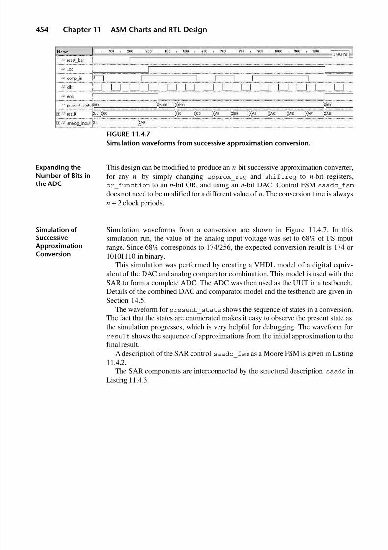
8/9/2019 VHDL for Engineers - Kenneth L. Short.pdf
http://slidepdf.com/reader/full/vhdl-for-engineers-kenneth-l-shortpdf 487/719
454 Chapter 11 ASM Charts and RTL Design
Expanding theNumber of Bits in
the ADC
This design can be modified to produce an n-bit successive approximation converter,for any n, by simply changing approx_reg and shiftreg to n-bit registers,
or_function to an n-bit OR, and using an n-bit DAC. Control FSM saadc_fsmdoes not need to be modified for a different value of n. The conversion time is alwaysn + 2 clock periods.
Simulation ofSuccessiveApproximationConversion
Simulation waveforms from a conversion are shown in Figure 11.4.7. In thissimulation run, the value of the analog input voltage was set to 68% of FS inputrange. Since 68% corresponds to 174/256, the expected conversion result is 174 or10101110 in binary.
This simulation was performed by creating a VHDL model of a digital equiv-alent of the DAC and analog comparator combination. This model is used with theSAR to form a complete ADC. The ADC was then used as the UUT in a testbench.Details of the combined DAC and comparator model and the testbench are given inSection 14.5.
The waveform for present_state shows the sequence of states in a conversion.The fact that the states are enumerated makes it easy to observe the present state asthe simulation progresses, which is very helpful for debugging. The waveform forresult shows the sequence of approximations from the initial approximation to thefinal result.
A description of the SAR control saadc_fsm as a Moore FSM is given in Listing11.4.2.
The SAR components are interconnected by the structural description saadc inListing 11.4.3.
FIGURE 11.4.7
Simulation waveforms from successive approximation conversion.

8/9/2019 VHDL for Engineers - Kenneth L. Short.pdf
http://slidepdf.com/reader/full/vhdl-for-engineers-kenneth-l-shortpdf 488/719
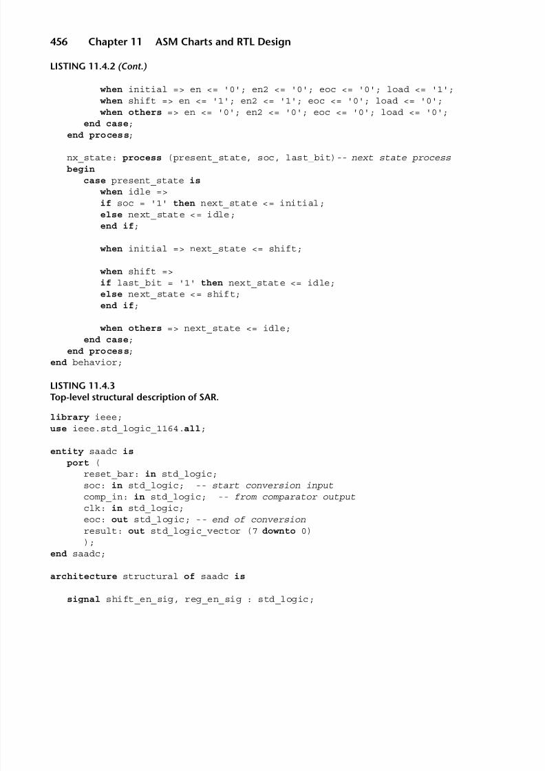
8/9/2019 VHDL for Engineers - Kenneth L. Short.pdf
http://slidepdf.com/reader/full/vhdl-for-engineers-kenneth-l-shortpdf 489/719
456 Chapter 11 ASM Charts and RTL Design
LISTING 11.4.2 (Cont.)
when initial => en <= '0'; en2 <= '0'; eoc <= '0'; load <= '1'; when shift => en <= '1'; en2 <= '1'; eoc <= '0'; load <= '0'; when others => en <= '0'; en2 <= '0'; eoc <= '0'; load <= '0';
end case;end process;
nx_state: process (present_state, soc, last_bit)-- next state processbegin
case present_state is
when idle =>if soc = '1' then next_state <= initial;else next_state <= idle;end if;
when initial => next_state <= shift;
when shift =>if last_bit = '1' then next_state <= idle;else next_state <= shift;end if;
when others => next_state <= idle;end case;
end process;end behavior;
LISTING 11.4.3Top-level structural description of SAR.
library ieee;use ieee.std_logic_1164.all;
entity saadc is
port (reset_bar: in std_logic;soc: in std_logic; -- start conversion inputcomp_in: in std_logic; -- from comparator outputclk: in std_logic;
eoc: out std_logic; -- end of conversionresult: out std_logic_vector (7 downto 0));
end saadc;
architecture structural of saadc is
signal shift_en_sig, reg_en_sig : std_logic;

8/9/2019 VHDL for Engineers - Kenneth L. Short.pdf
http://slidepdf.com/reader/full/vhdl-for-engineers-kenneth-l-shortpdf 490/719
Section 11.5 Sequential Multiplier Design 457
signal load_sig: std_logic;signal sr_sig, sar_sig, result_sig : std_logic_vector(7 downto 0);
begin
u0: entity shiftreg port map (clr_bar => reset_bar, load => load_sig,en => shift_en_sig, clk => clk, qout => sr_sig);
u1: entity approx_reg port map (d => result_sig, reset_bar => reset_bar,load => load_sig,
en1 => comp_in, en2 => reg_en_sig, clk => clk, qar => sar_sig);
u2: entity or_function port map (a => sr_sig, b => sar_sig,or_out => result_sig);
u3: entity saadc_fsm port map (clk => clk, reset_bar => reset_bar,soc => soc,last_bit => sr_sig(0), load => load_sig, en => shift_en_sig,
en2 => reg_en_sig, eoc => eoc);
result <= result_sig;
end structural;
1 1. 5 S EQ UE NT IA L M UL TI PL IE R D ES IG N
When we perform a binary multiplication by hand, we examine each bit of the multi-
plier in succession, starting with its least significant bit (Figure 11.5.1). If the multi-plier bit being examined is a 1, we write down a copy of the multiplicand as thepartial product resulting from that multiplier bit. If the multiplier bit is a 0, we writedown 0, as the corresponding partial product. The partial product resulting fromeach multiplier bit is written shifted left one bit position relative to the previouspartial product. This reflects the fact that each successive multiplier bit has aweight that is twice that of the bit to its right. After all the multiplier bits have
1110 multiplicand
1010 multiplier
0000 1st partial product
1110 2nd partial product
0000 3rd partial product
1110 4th partial product
10001100 product
FIGURE 11.5.1
Example of binary multiplication performed by hand.

8/9/2019 VHDL for Engineers - Kenneth L. Short.pdf
http://slidepdf.com/reader/full/vhdl-for-engineers-kenneth-l-shortpdf 491/719
458 Chapter 11 ASM Charts and RTL Design
been examined and all partial products recorded, the partial products are added toproduce the product.
If we create an architecture that directly maps this algoritm to hardware for a n-bitmultiplier and a n-bit multiplicand, it would require two n-bit registers to hold theoperands, n n-bit registers to hold the partial products, n – 1 n-bit adders, and a 2n-bit
register to hold the product.This hardware can be significantly reduced if the algorithm is modified so that, as
soon as each partial product is determined, it is added to a single register that accumu-lates the product. This allows the n n-bit registers used to hold the partial products andthe n – 1 n-bit adders to be replaced by a single n-bit adder. However, logic thatprovides the relative 1-bit displacement to the left for each partial product’s addition tothe accumulated product is required.
This 1-bit displacement to the left for the addition of each partial product to theaccumulated product can be efficiently accomplished by making the register thataccumulates the product a right shift register. Shifting the accumulated product to theright relative to the partial product after each addition is equivalent to shifting the partialproduct to the left relative to the accumulated product (Figure 11.5.2). The result is theclassic add and shift multiplication algorithm.
A block diagram of a data path for the modified multiplication algorithm using an8-bit multiplier and an 8-bit multiplicand is given in Figure 11.5.3.
FIGURE 11.5.2
Shifting the accumulated product right relative to the partial product.
product
n
n
n
nn
n
product_low
sum
1
multiplicand
product_high
carry
adder
D Q

8/9/2019 VHDL for Engineers - Kenneth L. Short.pdf
http://slidepdf.com/reader/full/vhdl-for-engineers-kenneth-l-shortpdf 492/719
Section 11.5 Sequential Multiplier Design 459
Multiplier Register First we specify each register and the combinational logic of the data path. Beforestarting a multiplication the operands are loaded. The multiplier is loaded into the8-bit register multiplier. During the alogrithm we will need to examine each bitof the multiplier in turn, starting with the least significant bit. This is facilitated bymaking this register a right shift register. The least significant bit of this register isavailable as the data path status signal x_lsb.
If the multiplier is zero at the start of a multiplication, the product will be zero andthere is no need to go through all the steps of the algorithm. Accordingly, the outputsof register multiplier or NORed to generate the status signal x_zero. This signalis asserted whenever the content of multiplier is zero.
MultiplicandRegister
The multiplicand is loaded into the 8-bit register multiplicand. If the multiplicandis zero at the start of a multiplication, the product will be zero and there is no need to
FIGURE 11.5.3
Data path for 8 x 8 multiplier.
8
8
8
8
8
88
8
prod_low
sum
1
multiplier
multiplicand
prod_high u2
carry
adder
load_x
shift_r_x
x_zero
load_y
load_h
shift_r_h
clear_l
shift_r_l
en_c
x_lsb
clear_hclr_c
0
4
4
loop_cntr
load_cntr
en_cntr
count_zero
1000
8
y_zero
carry_ff
u0 u6
u1
u5
u4 u3
8/9/2019 VHDL for Engineers - Kenneth L. Short.pdf
http://slidepdf.com/reader/full/vhdl-for-engineers-kenneth-l-shortpdf 493/719
460 Chapter 11 ASM Charts and RTL Design
go through all the steps of the algorithm. Accordingly, the outputs of register multi-plicand or NORed to generate the status signal y_zero. This signal is assertedwhenever the content of multiplicand is zero.
Product
AccumulatorRegisters
For an 8-bit multiplier and an 8-bit multiplicand a 16-bit register is needed to hold the
product. In Figure 11.5.3, this 16-bit register is comprised of two 8-bit registers:prod_high and prod_low. At the start of a multiplication we must clear both of theseregisters. Thus, each register has a clear input, clear_h and clear_l, respectively.
If the multiplier bit being examined is a 1, we must add the multiplicand to theaccumulated product. If it is a 0, we add zero to the accumulated product. This is equiv-alent to not performing an addition. Each successive addition of either the multiplicandor 0 must be made one bit position to the left relative to the accumulated product. Thisis accomplished by making registers prod_high and prod_low right shift registers.
Adder An 8-bit adder is required to add the multiplicand to the accumulated product. Theadder adder is a purely combinational circuit. Its inputs are the output from register
prod_high and the output from register multiplicand. The sum from adder isthe input to register prod_high. The adder’s carry is the input to carry_ff.
Carry Flip-flop The carry from an addition is part of the accumulated product. This carry must beshifted into prod_high when the accumulated product is shifted right. Accordingly,flip-flop carry_ff is needed to hold the carry.
Loop Counter Finally, the algorithm contains a loop and we need to count its iterations. This couldbe done as part of the FSM or as part of the data path. We have chosen to do this inthe data path by including a 4-bit counter named loop_cntr. We want to counteight interations. At the start of a multiplication, loop_cntr is loaded with the value8 and subsequently counted down to 0. The outputs of loop_cntr or NORed togenerate the status signal count_zero. This signal is asserted whenever the contentof loop_cntr is zero.
First Multiplier FSMBlock Symbol
Each of the components in the data path was individually specified. The inputs to theblock symbol for the FSM in Figure 11.5.4 are the status outputs from the data path,shown with open arrows, and the external inputs to the multiplier, shown with solidarrows. The control outputs from the FSM to the data path are shown with openarrows. These outputs are labeled with the name of the data path component input towhich they connect. The single external status output from the FSM is the signal
done and it is shown with a solid arrow.
First Multiplier ASMChart
An ASM chart for the multiplier’s FSM is given in Figure 11.5.5. The states areidle, start, ck_oprnds, ck_lsb, add, shift_r, and ck_count. This ASMchart is for a Moore FSM.
After system reset, the FSM stays in the idle state until the start_multiplyexternal input is asserted. When this input is asserted, the FSM transitions to thestart state at the next triggering clock edge.

8/9/2019 VHDL for Engineers - Kenneth L. Short.pdf
http://slidepdf.com/reader/full/vhdl-for-engineers-kenneth-l-shortpdf 494/719
Section 11.5 Sequential Multiplier Design 461
In state start, the signals to enable loading the multiplier, multiplicand,and loop_cntr and clearing the prod_high, prod_low, and carry_ff registersare asserted. On the next triggering clock edge these registers are loaded and cleared,respectively, and the FSM transitions to the ck_oprnds state.
In state ck_oprnds, if either multiplier or multiplicand is zero, x_zero ory_zero is asserted, the FSM transitions back to state idle on the next triggeringclock edge and the multiplication is complete. If neither multiplier or multi-plicand is zero, then the next state is ck_lsb.
In state ck_lsb, the next state transition is based on the value of the multiplier bitbeing examined. If x_lsb is 1, the transition is to the add state. Otherwise, thetransition is to the shift_r state.
In state add, signals to enable the carry_ff to store the carry and the prod_h
register to load the sum from the adder are asserted. On the next triggering clock edge these actions occur and the FSM transitions to the shift_r state.
In state shift_r, signals to enable prod_high and prod_low to shift right, thecarry_ff to be cleared, and the loop_cntr to be decremented are asserted. On thenext triggering clock edge these actions occur and the FSM transitions to the ck_count
state.
In state ck_count, the count_zero status signal is checked. If it is asserted themultiplication is complete and the transition is back to the idle state. Otherwise, thetransition is back to the ck_oprnds state and the multiplication continues.
SimplerMultiplicationASM Chart
In examining the FSM outputs asserted in each state of the ASM chart, it can be seenthat some outputs are asserted in only a single state. All of the outputs asserted inonly a single state can be replaced by a single output that is connected to all thecomponent inputs associated with the replaced output signals. For example, outputs
FIGURE 11.5.4
Multiplier FSM with data path control outputs labeled corresponding to datapath component input labels.
start_multiply
x_zero
load_x
shift_r_x
load_y
en_c
clear_h
load_h
shift_r_h
clear_l
shift_r_l
done
x_lsb
clk
rst_bar
clr_c
count_zero
load_cntr
en_cntr
y_zero
mult_fsm

8/9/2019 VHDL for Engineers - Kenneth L. Short.pdf
http://slidepdf.com/reader/full/vhdl-for-engineers-kenneth-l-shortpdf 495/719
462 Chapter 11 ASM Charts and RTL Design
load_x, load_y, clear_l, clear_h, and load_cntr are only asserted in statestart. All of these FSM outputs can be replaced by a single output named init.This output signal must be connected to the load_x, load_y, clear_l, clear_h,and load_cntr inputs of the appropriate data path components.
FIGURE 11.5.5
First ASM chart for multiplier FSM.
done
start_multiply
load_xload_yclr_c
clear_lclear_h
load_cntr
idle
start
x_zero ory_zero
0
0
1
en_c
load_h
x_lsb
shift_r_1shift_r_hshfit_r_x
clr_cen_cntr
0
1add
1
shift_r
count_zero01
ck_count
ck_oprnds
ck_lsb

8/9/2019 VHDL for Engineers - Kenneth L. Short.pdf
http://slidepdf.com/reader/full/vhdl-for-engineers-kenneth-l-shortpdf 496/719
Section 11.5 Sequential Multiplier Design 463
If two or more FSM outputs are asserted only in the same states, they can also becombined. A simplified ASM chart that reflects these kinds of simplifications isgiven in Figure 11.5.6
FIGURE 11.5.6
Simplified ASM chart of multiplier FSM.
done
start_multiply
initclr_c
idle
start
y_zero
x_zero or
0
0
1
en_c
load_h
x_lsb
shiftclr_c
en_cntr
0
1add
1
shift_r
count_zero01
ck_count
ck_oprnds
ck_lsb
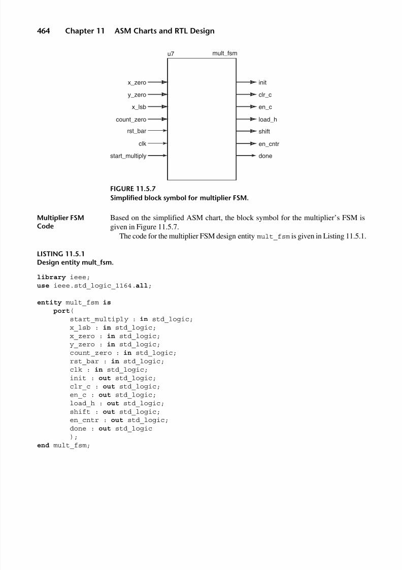
8/9/2019 VHDL for Engineers - Kenneth L. Short.pdf
http://slidepdf.com/reader/full/vhdl-for-engineers-kenneth-l-shortpdf 497/719
464 Chapter 11 ASM Charts and RTL Design
Multiplier FSMCode
Based on the simplified ASM chart, the block symbol for the multiplier’s FSM isgiven in Figure 11.5.7.
The code for the multiplier FSM design entity mult_fsm is given in Listing 11.5.1.
LISTING 11.5.1Design entity mult_fsm.
library ieee;
use ieee.std_logic_1164.all;
entity mult_fsm is
port(start_multiply : in std_logic;x_lsb : in std_logic;x_zero : in std_logic;y_zero : in std_logic;count_zero : in std_logic;rst_bar : in std_logic;clk : in std_logic;init : out std_logic;
clr_c : out std_logic;en_c : out std_logic;load_h : out std_logic;shift : out std_logic;en_cntr : out std_logic;done : out std_logic);
end mult_fsm;
FIGURE 11.5.7Simplified block symbol for multiplier FSM.
start_multiply
x_zero
en_c
load_h
shift
done
x_lsb
clk
rst_bar
clr_c
count_zero
init
en_cntr
y_zero
mult_fsmu7

8/9/2019 VHDL for Engineers - Kenneth L. Short.pdf
http://slidepdf.com/reader/full/vhdl-for-engineers-kenneth-l-shortpdf 498/719
Section 11.5 Sequential Multiplier Design 465
architecture behavioral of mult_fsm is
type state is (idle, start, ck_oprnds, ck_lsb, add, shift_r, ck_count);signal present_state, next_state : state;
begin
state_reg: process (clk, rst_bar)begin
if rst_bar = '0' then
present_state <= idle;elsif rising_edge(clk) then
present_state <= next_state;end if;
end process;
output_process: process (present_state)begin
-- set all outputs to unasserted values
init <= '0'; shift <= '0'; clr_c <= '0'; en_c <= '0';load_h <= '0'; en_cntr <= '0'; done <= '0';
case present_state is
when idle => done <= '1'; when start => init <= '1'; clr_c <= '1'; when ck_oprnds => null; when ck_lsb => null; when add => en_c <= '1'; load_h <= '1'; when shift_r => shift <= '1'; clr_c <= '1'; en_cntr <= '1'; when ck_count => null;
end case;end process;
nxt_state: process (present_state, start_multiply, x_lsb, x_zero,y_zero, count_zero)
begin
case present_state is
when idle =>if start_multiply = '0' then
next_state <= idle;else
next_state <= start;
end if;
when start => next_state <= ck_oprnds;
when ck_oprnds =>if (x_zero = '1' or y_zero = '1') then
next_state <= idle;
(Cont.)
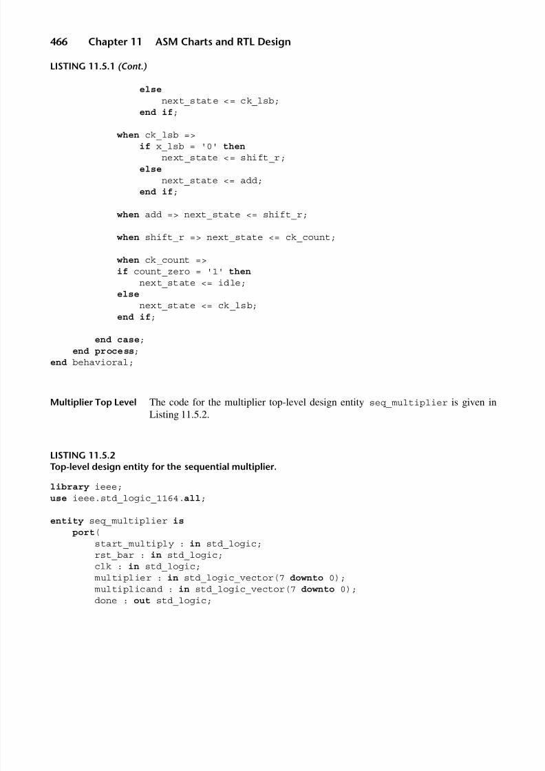
8/9/2019 VHDL for Engineers - Kenneth L. Short.pdf
http://slidepdf.com/reader/full/vhdl-for-engineers-kenneth-l-shortpdf 499/719
466 Chapter 11 ASM Charts and RTL Design
LISTING 11.5.1 (Cont.)
else
next_state <= ck_lsb;end if;
when ck_lsb =>if x_lsb = '0' then
next_state <= shift_r;else
next_state <= add;end if;
when add => next_state <= shift_r;
when shift_r => next_state <= ck_count;
when ck_count =>if count_zero = '1' then
next_state <= idle;else
next_state <= ck_lsb;end if;
end case;end process;
end behavioral;
Multiplier Top Level The code for the multiplier top-level design entity seq_multiplier is given inListing 11.5.2.
LISTING 11.5.2Top-level design entity for the sequential multiplier.
library ieee;use ieee.std_logic_1164.all;
entity seq_multiplier isport(
start_multiply : in std_logic;rst_bar : in std_logic;clk : in std_logic;multiplier : in std_logic_vector(7 downto 0);multiplicand : in std_logic_vector(7 downto 0);done : out std_logic;

8/9/2019 VHDL for Engineers - Kenneth L. Short.pdf
http://slidepdf.com/reader/full/vhdl-for-engineers-kenneth-l-shortpdf 500/719
Section 11.5 Sequential Multiplier Design 467
product : out std_logic_vector(15 downto 0));
end seq_multiplier;
architecture behavioral of seq_multiplier is
signal init, shift, clr_c, en_c, load_h, en_cntr : std_logic;signal x_lsb, x_zero, y_zero : std_logic;signal cy_reg, carry, count_zero : std_logic;signal multiplicand_reg, product_l_sig, product_h_sig,sum : std_logic_vector(7 downto 0);
begin
u0: entity multiplier port map (d => multiplier, load_x => init,shift_r_x => shift,
clk => clk, rst_bar => rst_bar, x_lsb => x_lsb, x_zero => x_zero);
u1: entity multiplicand port map (d => multiplicand, load_y => init,clk => clk,
rst_bar => rst_bar, q => multiplicand_reg, y_zero => y_zero);
u2: entity prod_low port map (si => product_h_sig(0), clear_l => init,shift_r_l => shift,
clk => clk, rst_bar => rst_bar, q => product_l_sig(7 downto 0));
u3: entity prod_high port map (d => sum, load_h => load_h, si => cy_reg,shift_r_h => shift, clear_h => init, clk => clk, rst_bar => rst_bar,q => product_h_sig);
u4: entity carry_ff port map (d => carry, enff => en_c, clrff => clr_c,clk => clk, rst_bar => rst_bar, q => cy_reg);
u5: entity adder port map (a => product_h_sig, b => multiplicand_reg,sum => sum, carry => carry);
u6: entity loop_cntr port map (load_cntr => init, en_cntr => en_cntr,clk => clk, rst_bar => rst_bar, count_zero => count_zero);
u7: entity mult_fsm port map (start_multiply => start_multiply,x_lsb => x_lsb, x_zero => x_zero, y_zero => y_zero,
count_zero => count_zero, rst_bar => rst_bar, clk => clk, init => init,clr_c => clr_c, en_c => en_c, load_h => load_h, shift => shift,en_cntr => en_cntr, done => done);
product(7 downto 0) <= product_l_sig;product(15 downto 8) <= product_h_sig;
end behavioral;

8/9/2019 VHDL for Engineers - Kenneth L. Short.pdf
http://slidepdf.com/reader/full/vhdl-for-engineers-kenneth-l-shortpdf 501/719
468 Chapter 11 ASM Charts and RTL Design
PROBLE MS
11.1 List each of the basic ASM chart elements and state its purpose.
11.2 For each of the state diagrams in Figure 10.2.1 draw an equivalent ASM chart.
11.3 For the state diagram in Figure 10.5.4 draw an equivalent ASM chart.11.4 For the state diagram in Figure 10.8.2 draw an equivalent ASM chart.
11.5 For the state diagram in Problem 10.22 draw an equivalent ASM chart.
11.6 Write a VHDL description of the component approx_reg. See “Component approx_reg” onpage 449.
11.7 Write a VHDL description of the component shiftreg. See “Component shiftreg” onpage 449.
11.8 Write a VHDL description of the component or_function. See “Component or_function”on page 449.
11.9 Compile and simulate the successive approximation algorithm in Listing 11.4.1. Attempt tosynthesize this description and describe the results of this attempt.
11.10 Create a state diagram and an ASM chart for a Mealy version of the SA FSM corresponding toFigure 11.4.6. Does the Mealy version have fewer states? If so, explain qualitatively how thisaffects the performance of the ADC as its number of bits is increased.
11.11 Create a RTL architecture for a direct (one-to-one) implementation of the successiveapproximation algorithm as described in Figure 11.4.2 and Listing 11.4.1. That is, use a singleregister with appropriate combinational logic and a FSM. Compare the efficiency andperformance of the architecture with that in Figure 11.4.4.
11.12 Draw a version of Figure 11.5.1 that illustrates a multiplication using the same operand valuesbut using an accumulated product that is shifted to the right after each addition.
11.13 Write the code for each of the design entities in Figure 11.5.3. Use information from Listing11.5.2 to determine the names of the ports for each design entity. Note that the NOR gates arepart of their associated design entities and do not represent separate design entities.
11.14 Create an ASM chart for a Mealy FSM for the sequential multiplier. Does this ASM chart havefewer states than the Moore FSM chart in Figure 11.5.4?
11.15 Write the code for the Mealy FSM corresponding to the ASM chart from Problem 11.14.
8/9/2019 VHDL for Engineers - Kenneth L. Short.pdf
http://slidepdf.com/reader/full/vhdl-for-engineers-kenneth-l-shortpdf 502/719
469
Chapter 12
Subprograms
VHDL subprograms are similar to subprograms in conventional programminglanguages. A subprogram is an encapsulated sequence of sequential statements thatdefine an algorithm. The algorithm uses the values of input parameters, passed to thesubprogram when it is called, to compute results or cause some desired effect.
The actual code for a subprogram appears only once in the text of a program.However, the subprogram can be executed by calling it from anywhere in the program.Unlike subprograms in conventional programming languages, VHDL subprograms canalso be executed as concurrent statements.
12 . 1 SU BP RO G RAMS
Subprograms simplify the organization of descriptions by providing informationhiding. Designs that use subprograms are more modular and compact. As a result,they are easier to read and understand. Writing a description is further simplified byreusing previously written and verified subprograms. This not only reduces the timerequired to write a description, but also reduces errors.
The main use of subprograms is to perform common and frequently repeatedoperations. While this use makes a program more modular, subprograms are not theprimary mechanism for producing hierarchy in synthesizable VHDL descriptions.Instead, design entities serve that purpose. Subprograms are not design units and,therefore, they cannot be separately compiled.
Kinds ofSubprograms
VHDL provides two kinds of subprograms; functions and procedures. A function
computes and returns a single value. This value is computed using the values of

8/9/2019 VHDL for Engineers - Kenneth L. Short.pdf
http://slidepdf.com/reader/full/vhdl-for-engineers-kenneth-l-shortpdf 503/719
470 Chapter 12 Subprograms
parameters passed to the function when it is called. A function is called from anexpression. The value returned by a function is used in the expression thatcontains the call. An expression containing a function call can be part of either asequential or concurrent statement. However, all statements within a function aresequential.
A procedure can return one or more values, or it may return no values and be usedonly for its effect. A procedure call is a statement. It can appear in a process oranother subprogram as a sequential statement. Or, it can appear alone in an archi-tecture body as a concurrent statement. However, all statements within a procedureare sequential.
ConcurrentSubprogramCalls Example
Before considering functions and procedures in detail, we look at an example thatincludes a function and a procedure that are called using concurrent statements. Inthis example, these subprograms are used like components in a mixed architecture.
The logic diagram for a positive-level D latch comprised of NAND gates is shown
in Figure 12.1.1.For instructional purposes, the D latch description in Listing 12.1.1 has each
NAND component implemented in a different way:
u1: concurrent signal assignment statement (nand_2csa)u2: component instantiation statement (nand_2c)u3: process statement (nand_2)u4: function in a concurrent signal assignment statement (nand_2f)u5: concurrent procedure call statement (nand_2p)
While this is certainly not an efficient way to describe a D latch, it illustrates how anumber of different kinds of concurrent statements can each implement an identicaloperation. It also illustrates how functions and procedures use signals to commu-nicate with other concurrent statements.
FIGURE 12.1.1
Logic diagram for a D latch composed of two-input NAND gates.
du2
u3
u4
u5u1
s1s3
s2
s4
s5
clk
q_bar
q
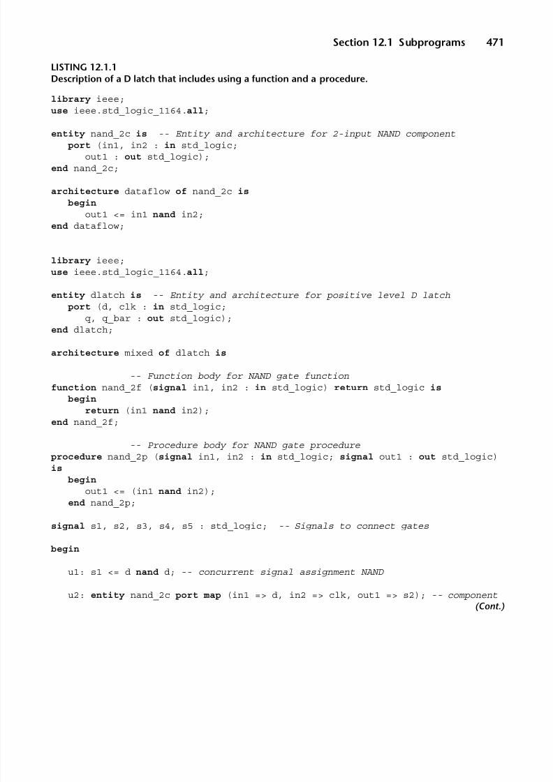
8/9/2019 VHDL for Engineers - Kenneth L. Short.pdf
http://slidepdf.com/reader/full/vhdl-for-engineers-kenneth-l-shortpdf 504/719
Section 12.1 Subprograms 471
LISTING 12.1.1Description of a D latch that includes using a function and a procedure.
library ieee;use ieee.std_logic_1164.all;
entity nand_2c is -- Entity and architecture for 2-input NAND componentport (in1, in2 : in std_logic;
out1 : out std_logic);end nand_2c;
architecture dataflow of nand_2c is
begin
out1 <= in1 nand in2;end dataflow;
library ieee;use ieee.std_logic_1164.all;
entity dlatch is -- Entity and architecture for positive level D latchport (d, clk : in std_logic;
q, q_bar : out std_logic);end dlatch;
architecture mixed of dlatch is
-- Function body for NAND gate functionfunction nand_2f (signal in1, in2 : in std_logic) return std_logic is
begin
return (in1 nand in2);end nand_2f;
-- Procedure body for NAND gate procedureprocedure nand_2p (signal in1, in2 : in std_logic; signal out1 : out std_logic)is
begin
out1 <= (in1 nand in2);end nand_2p;
signal s1, s2, s3, s4, s5 : std_logic; -- Signals to connect gates
begin
u1: s1 <= d nand d; -- concurrent signal assignment NAND
u2: entity nand_2c port map (in1 => d, in2 => clk, out1 => s2); -- component(Cont.)
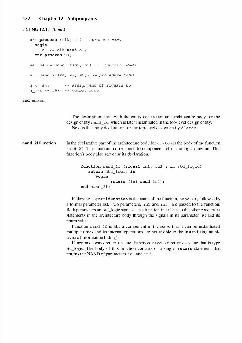
8/9/2019 VHDL for Engineers - Kenneth L. Short.pdf
http://slidepdf.com/reader/full/vhdl-for-engineers-kenneth-l-shortpdf 505/719
472 Chapter 12 Subprograms
LISTING 12.1.1 (Cont.)
u3: process (clk, s1) -- process NAND begin
s3 <= clk nand s1;end process u3;
u4: s4 <= nand_2f(s2, s5); -- function NAND
u5: nand_2p(s4, s3, s5); -- procedure NAND
q <= s4; -- assignment of signals to q_bar <= s5; -- output pins
end mixed;
The description starts with the entity declaration and architecture body for thedesign entity nand_2c, which is later instantiated in the top-level design entity.
Next is the entity declaration for the top-level design entity dlatch.
nand_2f Function In the declarative part of the architecture body for dlatch is the body of the functionnand_2f. This function corresponds to component u4 in the logic diagram. Thisfunction’s body also serves as its declaration.
function nand_2f (signal in1, in2 : in std_logic)
return std_logic isbegin
return (in1 nand in2);end nand_2f;
Following keyword function is the name of the function, nand_2f, followed bya formal parameter list. Two parameters, in1 and in2, are passed to the function.Both parameters are std_logic signals. This function interfaces to the other concurrentstatements in the architecture body through the signals in its parameter list and itsreturn value.
Function nand_2f is like a component in the sense that it can be instantiated
multiple times and its internal operations are not visible to the instantiating archi-tecture (information hiding).
Functions always return a value. Function nand_2f returns a value that is typestd_logic. The body of this function consists of a single return statement thatreturns the NAND of parameters in1 and in2.
8/9/2019 VHDL for Engineers - Kenneth L. Short.pdf
http://slidepdf.com/reader/full/vhdl-for-engineers-kenneth-l-shortpdf 506/719
Section 12.2 Functions 473
nand_2p Procedure Following the function body for nand_2f is the procedure body for procedurenand_2p:
procedure nand_2p (signal in1, in2 : in std_logic;signal out1 : out std_logic) is
beginout1 <= (in1 nand in2);
end nand_2p;
Following keyword procedure is the name of the procedure, nand_2p. Theformal parameter list specifies three parameters, all std_logic signals. Parametersin1 and in2 are inputs and parameter out1 is an output. Procedure nand_2p
contains a single sequential signal assignment statement that assigns out1 theNAND of parameters in1 and in2.
Also declared in the architecture body’s declarative part are signals s1 through s5.These signals provide the communications between “components” u1 through u5.
In the statement part of the top-level architecture are seven concurrent statements.The first five correspond to the “components” u1 through u5. The last two assign thevalues of signals s4 and s5 to output ports q and q_bar, respectively.
u1, u2, and u3 are, respectively, a concurrent signal assignment statement, acomponent instantiation statement, and a process statement.
Calling a function or procedure in this example is analogous to instantiating acomponent. A function can be used to instantiate a “component” that has a singleoutput. The function call must be part of an expression. Statement u4 is a concurrentsignal assignment that assigns the value returned by function nand_2f to signal s4.In this function call, actual parameters, signals s2 and s5, replace formal parameters
in1 and in2, respectively. This function is called to update the value of s4 wheneverthere is an event on either s2 or s5.
Concurrent procedure call statement u5 calls procedure nand_2p. Actualparameter signals s4, s3, and s5 replace formal parameters in1, in2, and out1,respectively, of the procedure body. The procedure is called whenever there is anevent on input parameters s4 or s3. When called, nand_2p updates the value of s5.
12 .2 FU N CT I O N S
A function can be considered a generalized form of an operator and used to define anew operator. A function is called in an expression. When called, a function calcu-lates and returns a result. The definition of a function can be given in two parts: afunction declaration and a function body. The function declaration defines thefunction’s calling conventions and is optional.
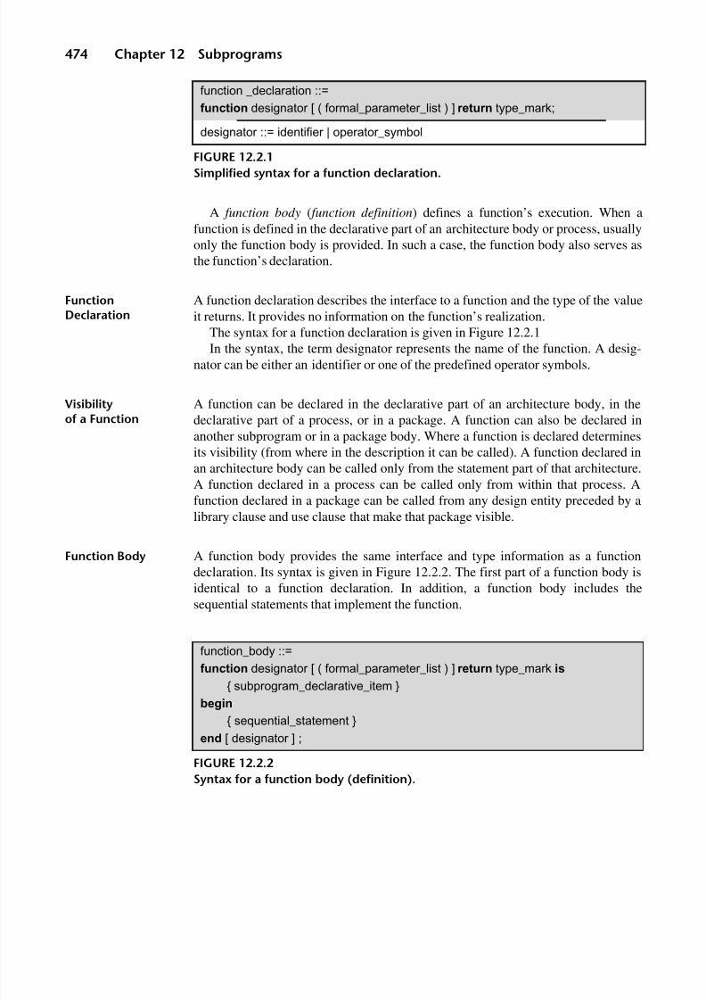
8/9/2019 VHDL for Engineers - Kenneth L. Short.pdf
http://slidepdf.com/reader/full/vhdl-for-engineers-kenneth-l-shortpdf 507/719
474 Chapter 12 Subprograms
A function body ( function definition) defines a function’s execution. When afunction is defined in the declarative part of an architecture body or process, usuallyonly the function body is provided. In such a case, the function body also serves asthe function’s declaration.
FunctionDeclaration
A function declaration describes the interface to a function and the type of the valueit returns. It provides no information on the function’s realization.
The syntax for a function declaration is given in Figure 12.2.1In the syntax, the term designator represents the name of the function. A desig-nator can be either an identifier or one of the predefined operator symbols.
Visibilityof a Function
A function can be declared in the declarative part of an architecture body, in thedeclarative part of a process, or in a package. A function can also be declared inanother subprogram or in a package body. Where a function is declared determinesits visibility (from where in the description it can be called). A function declared inan architecture body can be called only from the statement part of that architecture.A function declared in a process can be called only from within that process. A
function declared in a package can be called from any design entity preceded by alibrary clause and use clause that make that package visible.
Function Body A function body provides the same interface and type information as a functiondeclaration. Its syntax is given in Figure 12.2.2. The first part of a function body isidentical to a function declaration. In addition, a function body includes thesequential statements that implement the function.
function _declaration ::=
function designator [ ( formal_parameter_list ) ] return type_mark;
designator ::= identifier | operator_symbol
FIGURE 12.2.1
Simplified syntax for a function declaration.
function_body ::=
function designator [ ( formal_parameter_list ) ] return type_mark is{ subprogram_declarative_item }
begin
{ sequential_statement }
end [ designator ] ;
FIGURE 12.2.2
Syntax for a function body (definition).

8/9/2019 VHDL for Engineers - Kenneth L. Short.pdf
http://slidepdf.com/reader/full/vhdl-for-engineers-kenneth-l-shortpdf 508/719
Section 12.2 Functions 475
In Listing 12.1.1, function nand_2f is defined in the declarative part of archi-tecture mixed. This function body serves as both the declaration and body for thisfunction. Function nand_2f is visible only in architecture mixed.
A function’s designator is either an identifier or one of the predefined VHDLoperator symbols. A VHDL operator symbol is used when the purpose of the function
is to overload the operator. Overloading of operators is discussed in Section 12.5.
Formal Parameters As seen in Listing 12.1.1, a formal parameter list is somewhat akin to an entity’s portinterface list. Formal parameters are simply placeholders. The names of the formalparameters are used in the statements inside a function to refer to the values that arepassed as actual parameters (arguments) when the function is called.
As seen in Figure 12.2.1, the parameter list for a function is optional. However,the use of parameters makes a function more general, so that it can perform itsalgorithm using different data each time it is called.
The formal_parameter_list is the list of parameters passed to the function. It has
the simplified form given in Figure 12.2.3.
Formal ParameterClass
Interface declarations in the formal parameter list are separated by semicolons. A formalparameter’s class and mode determine how access to that parameter is implemented.
A formal parameter’s class indicates the class of the parameter within the function.That is, how the parameter can be referenced in the statement part of the functionbody. In general, the class of a formal parameter of a function may be either constant,signal, or file. Parameters of class file have no mode. Since files are not used asparameters in functions that are synthesized, they are not discussed further in thischapter.
The default class of a parameter passed to a function is constant. However, the
actual parameter that replaces a formal constant parameter when a function is calledcan be an expression, constant, variable, or signal.
Formal ParameterMode
The mode of a formal parameter specifies how the parameter may be accessedwithin the statement part of the function body. The syntax for the formal parameterlist indicates that the mode of a parameter used in a function must be in, and that itsspecification is optional. Because their mode is in, function parameter values canonly be read in a function body; they cannot be written.
formal_parameter_list ::=
interface_declaration { ; interface_declaration }
interface_declaration ::=
[ constant ] identifier_list : [ in ] subtype_indication [ := static _expression ]
| [signal] identifier_list : [ in ] subtype_indication [ := static _expression ]
FIGURE 12.2.3
Simplified formal parameter list for a function.

8/9/2019 VHDL for Engineers - Kenneth L. Short.pdf
http://slidepdf.com/reader/full/vhdl-for-engineers-kenneth-l-shortpdf 509/719
476 Chapter 12 Subprograms
Taking advantage of the defaults, the body of the function in Listing 12.1.1 couldbe written as:
function nand_2f (in1, in2 :std_logic)return std_logic isbegin
return (in1 nand in2);end nand_2f;
FunctionParameterDefault Values
For formal parameters of class constant and mode in, optional default values can bespecified in the formal parameter list. If a default is specified, an actual value can beomitted in the call. This can be done by using the keyword open for the actualparameter in the call. Another method of omitting the actual value is simply to notassociate any value with the formal. In this case, any formal parameter for which novalue is specified must appear in the parameter list after all formals for which valuesare specified.
Declarative Partof a Function
Since within a function’s body formal parameters cannot be modified, variables mayneed to be declared in a function to store intermediate values. Variables declared in
a function are initialized on each call to the function. Values of variables do not
persist from one call to the next. Functions only use variables to store intermediatevalues. Since a variable is updated immediately after assignment, its value can bereturned to the function’s caller. Neither shared variables nor signals can be declaredin a function.
Other items that can be declared in a function are types, subtypes, constants, andnested subprograms.
Statement Partof a Function
Within the statement part of a function body all statements must be sequential. Withthe exception of wait statements, any of the sequential statements that we have previ-ously considered can be used. Functions cannot contain wait statements. If afunction calls a procedure, the procedure cannot contain a wait statement. Allfunctions execute in zero simulation time.
Return Statement A function can have only one return value and it must be of the type specified in thefunction’s declaration. A function must contain at least one return statement. A
return statement has the form given in Figure 12.2.4.
return_statement ::=
return [ expression ] ;
FIGURE 12.2.4
Syntax for a return statement.

8/9/2019 VHDL for Engineers - Kenneth L. Short.pdf
http://slidepdf.com/reader/full/vhdl-for-engineers-kenneth-l-shortpdf 510/719
Section 12.2 Functions 477
The value represented by the expression is the value returned by the function. The
value returned can be assigned to a signal or variable of the return type, or used to
build an expression of that type.
A function can have more than one return statement. This often occurs whenreturn statements are used in different branches of an if statement or case statement.
Multiple return statements may also appear in a loop, to break out of the loop andthen after the loop, to handle the situation where the loop is completed without areturn statement within the loop being executed.
When a return statement is executed, the flow of control continues with completionof the evaluation of the statement containing the function call.
Function Call The caller passes parameters to a function as part of a function call. A function callconsists of the function name followed by a list of actual parameters. The functioncall can appear alone on the right-hand side of an assignment statement, or as part of a more complex expression.
A function declared in the declarative part of an architecture body can be called inthe statement part of the architecture body using a concurrent statement, or can becalled by a sequential statement in a process in the architecture body. A functiondeclared in the declarative part of a process can only be called from within that process.
When a function call appears in a concurrent signal assignment statement, it isexecuted whenever there is an event on a signal in its parameter list. In contrast, afunction in a process is executed only when the statement containing the functioncall is reached during the sequential execution of the process’s statements.
Actual Parameters Actual parameters are the names of the actual data objects whose values are mappedto the formal parameters when a function is called. The function uses the values of the actual parameters in its execution.
ParameterMatching
The class of the actual parameters must match the class of the formal parameters,except when the formal parameter’s class is constant. A constant class formal
parameter can be replaced by an actual parameter that is either an expression,
constant, variable, or signal. The type of the actual parameter must match the type
of the formal parameter.
Formal parameters are specified with a type. An actual parameter that is a subtypeof the type of a formal parameter can also be passed. This allows a function writtenin terms of base type formal parameters to handle actuals that are the base type or
any of its subtypes.
ParameterAssociation
Actual parameters are associated with formal parameters using either positional
association or named association. Association is expressed in the same way as in theport map of a component instantiation.
The single value returned from a function called as an operand from within anexpression replaces the function call itself within the expression.
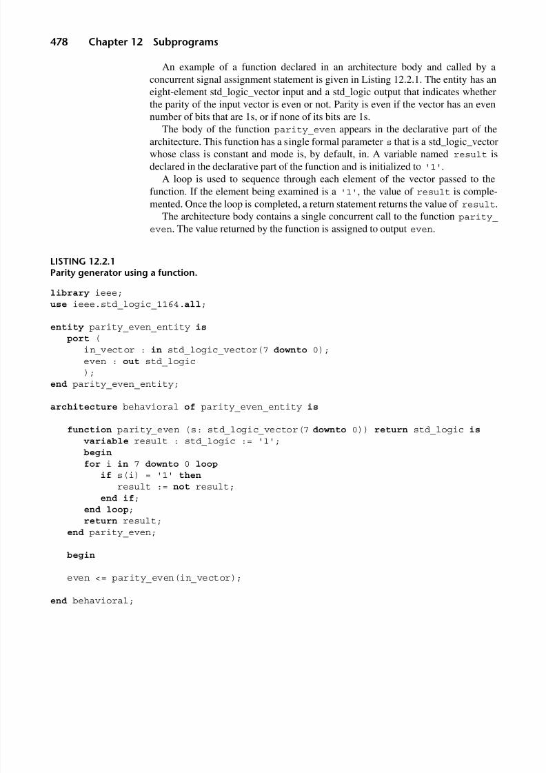
8/9/2019 VHDL for Engineers - Kenneth L. Short.pdf
http://slidepdf.com/reader/full/vhdl-for-engineers-kenneth-l-shortpdf 511/719
478 Chapter 12 Subprograms
An example of a function declared in an architecture body and called by aconcurrent signal assignment statement is given in Listing 12.2.1. The entity has aneight-element std_logic_vector input and a std_logic output that indicates whetherthe parity of the input vector is even or not. Parity is even if the vector has an evennumber of bits that are 1s, or if none of its bits are 1s.
The body of the function parity_even appears in the declarative part of thearchitecture. This function has a single formal parameter s that is a std_logic_vectorwhose class is constant and mode is, by default, in. A variable named result isdeclared in the declarative part of the function and is initialized to '1'.
A loop is used to sequence through each element of the vector passed to thefunction. If the element being examined is a '1', the value of result is comple-mented. Once the loop is completed, a return statement returns the value of result.
The architecture body contains a single concurrent call to the function parity_
even. The value returned by the function is assigned to output even.
LISTING 12.2.1Parity generator using a function.
library ieee;use ieee.std_logic_1164.all;
entity parity_even_entity is
port (in_vector : in std_logic_vector(7 downto 0);even : out std_logic);
end parity_even_entity;
architecture behavioral of parity_even_entity is
function parity_even (s: std_logic_vector(7 downto 0)) return std_logic is
variable result : std_logic := '1';begin
for i in 7 downto 0 loop
if s(i) = '1' then
result := not result;end if;
end loop;
return result;end parity_even;
begin
even <= parity_even(in_vector);
end behavioral;
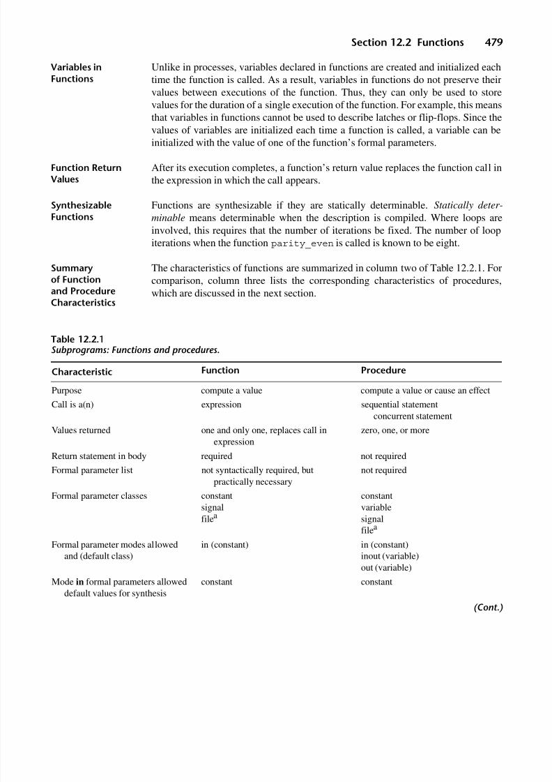
8/9/2019 VHDL for Engineers - Kenneth L. Short.pdf
http://slidepdf.com/reader/full/vhdl-for-engineers-kenneth-l-shortpdf 512/719
Section 12.2 Functions 479
Variables inFunctions
Unlike in processes, variables declared in functions are created and initialized eachtime the function is called. As a result, variables in functions do not preserve theirvalues between executions of the function. Thus, they can only be used to storevalues for the duration of a single execution of the function. For example, this meansthat variables in functions cannot be used to describe latches or flip-flops. Since the
values of variables are initialized each time a function is called, a variable can beinitialized with the value of one of the function’s formal parameters.
Function ReturnValues
After its execution completes, a function’s return value replaces the function call inthe expression in which the call appears.
SynthesizableFunctions
Functions are synthesizable if they are statically determinable. Statically deter-
minable means determinable when the description is compiled. Where loops areinvolved, this requires that the number of iterations be fixed. The number of loopiterations when the function parity_even is called is known to be eight.
Summaryof Functionand ProcedureCharacteristics
The characteristics of functions are summarized in column two of Table 12.2.1. Forcomparison, column three lists the corresponding characteristics of procedures,which are discussed in the next section.
Table 12.2.1Subprograms: Functions and procedures.
Characteristic Function Procedure
Purpose compute a value compute a value or cause an effect
Call is a(n) expression sequential statementconcurrent statement
Values returned one and only one, replaces call inexpression
zero, one, or more
Return statement in body required not required
Formal parameter list not syntactically required, butpractically necessary
not required
Formal parameter classes constantsignalfilea
constantvariablesignal
filea
Formal parameter modes allowedand (default class)
in (constant) in (constant)inout (variable)out (variable)
Mode in formal parameters alloweddefault values for synthesis
constant constant
(Cont.)

8/9/2019 VHDL for Engineers - Kenneth L. Short.pdf
http://slidepdf.com/reader/full/vhdl-for-engineers-kenneth-l-shortpdf 513/719
480 Chapter 12 Subprograms
12 . 3 PR OC E D U R E S
Procedures are like functions, in that they are encapsulated sequences of sequentialstatements. However, there are several important differences.
ProcedureDeclaration Like a function, the definition of a procedure can be given in two parts: a proceduredeclaration and a procedure body. A procedure declaration defines a procedure’scalling convention and is optional. It provides no information on the procedure’simplementation. A procedure declaration has the form shown in Figure 12.3.1.
Procedure Body A procedure body ( procedure definition) provides the same interface and type infor-mation as a procedure declaration. In addition, a procedure body includes thesequential statements that define the procedure’s implementation.
When a procedure is defined in the declarative part of an architecture or a process,usually only the procedure body is provided. In such cases, the procedure body alsoserves as the procedure’s declaration. The syntax for a procedure body is given in
Figure 12.3.2. A procedure’s designator is always an identifier; no operator symbolsare allowed.
Table 12.2.1 (Cont.)
Characteristic Function Procedure
Formal parameter andassociated actual parameters
formal => actual
constant => expressionb
signal => signal
file => filea
constant => expressionvariable => variable
signal => signalfile => filea
Declaration of signals insubprogram body
not allowed not allowed
Signal assignments in subprogrambody
not allowed allowed, including visible signals notpassed as parameters
wait statements not allowed at all not allowed if procedure is called by afunction or a process with asensitivity lista
synthesizable? if statically determinable and no fileparameters
if statically determinable and no fileparameters or wait statements
aFiles are not supported for synthesis.bSince the actual parameter can be an expression, it can be a variable, signal, or constant.
procedure_declaration ::=
procedure identifier [ ( formal_parameter_list ) ]
FIGURE 12.3.1
Syntax for a procedure declaration.
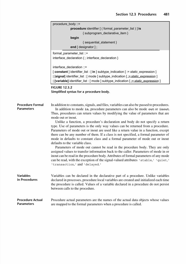
8/9/2019 VHDL for Engineers - Kenneth L. Short.pdf
http://slidepdf.com/reader/full/vhdl-for-engineers-kenneth-l-shortpdf 514/719
Section 12.3 Procedures 481
Procedure FormalParameters
In addition to constants, signals, and files, variables can also be passed to procedures.In addition to mode in, procedure parameters can also be mode out or inout.
Thus, procedures can return values by modifying the value of parameters that aremode out or inout.
Unlike a function, a procedure’s declaration and body do not specify a returntype. Use of parameters is the only way values can be returned from a procedure.Parameters of mode out or inout are used like a return value in a function, except
there can be any number of them. If a class is not specified, a formal parameter of mode in defaults to constant class and a formal parameter of mode out or inoutdefaults to the variable class.
Parameters of mode out cannot be read in the procedure body. They are onlyassigned values to transfer information back to the caller. Parameters of mode in orinout can be read in the procedure body. Attributes of formal parameters of any modecan be read, with the exception of the signal-valued attributes 'stable,' 'quiet,''transaction,' and 'delayed.'
Variablesin Procedures
Variables can be declared in the declarative part of a procedure. Unlike variablesdeclared in processes, procedure local variables are created and initialized each timethe procedure is called. Values of a variable declared in a procedure do not persistbetween calls to the procedure.
Procedure ActualParameters
Procedure actual parameters are the names of the actual data objects whose valuesare mapped to the formal parameters when a procedure is called.
procedure_body ::=
procedure identifier [ ( formal_parameter_list ) ] is
{ subprogram_declarative_item }
begin
{ sequential_statement }
end [ designator ] ;
formal_parameter_list ::=
interface_declaration { ; interface_declaration }
interface_declaration ::=
[ constant ] identifier_list : [ in ] subtype_indication [ := static _expression ]
| [signal] identifier_list : [ mode ] subtype_indication [ := static _expression ]
| [variable] identifier_list : [ mode ] subtype_indication [ := static _expression ]
FIGURE 12.3.2Simplified syntax for a procedure body.
8/9/2019 VHDL for Engineers - Kenneth L. Short.pdf
http://slidepdf.com/reader/full/vhdl-for-engineers-kenneth-l-shortpdf 515/719
482 Chapter 12 Subprograms
Signal ActualParameters
Signals cannot be declared in a procedure. However, signals can be passed to aprocedure as parameters and assigned new values within the procedure. A signalformal parameter can be mode in, out, or inout.
Pass by Value When a scalar constant or variable is passed to a procedure during a procedure call,it is passed by value. A copy of the value of the actual data object is passed to theformal parameter and used by statements in the procedure body. The value of aformal variable parameter of mode out or inout is passed back to the correspondingactual parameter when the procedure returns. Arrays or records can be passedeither by value or by reference; the IEEE Std 1076 standard allows either methodof implementation.
Pass by Reference The passing of signal parameters is more complicated. Instead of passing a value, areference to the signal, the driver of the signal, or both are passed based on the mode
of the signal.When a caller passes a signal parameter of mode in, instead of passing the valueof the signal, a reference to the signal object itself is passed . Any reference to theformal parameter within the procedure is like a reference to the actual signal.
A consequence of this is that, if a procedure executes a wait statement, a signal’svalue may be different after the wait statement completes and the procedureresumes. This fact is often used to advantage by procedures in testbenches. Thisbehavior differs from that of a constant parameter of mode in, which has the samevalue throughout the execution of a procedure. When a procedure executes a waitstatement it is the calling process that actually suspends.
When a caller passes a signal of mode out, the procedure is passed a reference to
the driver of the signal. When the procedure performs a signal assignment to theformal parameter, the transaction is scheduled on the driver for the actual signal.
When a caller passes a signal of mode inout, both a reference to the signal and areference to its driver are passed to the procedure.
Side Effects It is possible for a procedure to read or write signals or variables that are not in itsparameter list. A procedure’s reading or writing a signal or variable that is not inits parameter list is called a side effect . A procedure can have a read side effect onany signal or variable visible to the procedure. Whether a procedure can have awrite side effect on a signal or variable depends on where the procedure is
declared. A procedure declared in the declarative part of a process can have awrite side effect on any signal or variable visible to the procedure. A proceduredeclared in an architecture’s declarative part or in a package cannot have a writeside affect on a signal.
The reason for creating a procedure with side effects is to limit the number of parameters in its formal parameter list. However, using procedures with side effectsis not considered good programming practice. Such procedures are not very readable

8/9/2019 VHDL for Engineers - Kenneth L. Short.pdf
http://slidepdf.com/reader/full/vhdl-for-engineers-kenneth-l-shortpdf 516/719
Section 12.3 Procedures 483
and can be difficult to reuse, because one or more of the procedure’s side effects maybe overlooked.
SequentialProcedure Call
A procedure call is a statement. A procedure can be called from within a process oranother subprogram. Such a call is a sequential procedure call. In a process, a
procedure is called when the call statement is reached in the sequential execution of statements in the process. A sequential procedure call is equivalent to insertinginline, at the call statement, the code in the procedure’s body.
A procedure that uses mode out or inout parameters that are variables can only
be called by a sequential procedure call. Furthermore, these parameters cannot be
used to assign values to signals.
Return Statementsin Procedures
When the last statement in a procedure is completed, the procedure returns. If theprocedure call was sequential, the flow of control returns to the statement followingthe call. A return statement is not required.
However, a return statement can be used to return from the middle of a procedure.
When a return statement is used in a procedure, it does not specify a return value.Execution of the return statement immediately terminates the procedure and returnscontrol to the caller.
When a procedure returns, the value of any formal parameters of mode out orinout are copied back to the corresponding actual parameters, transferring infor-mation back to the caller.
ConcurrentProcedure Call
A procedure call can also exist alone in an architecture body as a concurrent
procedure call. As a shorthand for component instantiation, procedures can representcomponents with multiple outputs. The procedure in a concurrent procedure call is
called whenever there is an event on a signal that is an input parameter (mode in orinout) to the procedure. The parameter list of a concurrent procedure cannot
contain a variable, since a variable cannot exist outside of a process.Synthesizeable procedures cannot have wait statements. In contrast, nonsynthe-
sizeable procedures can. However, since a process cannot have both a sensitivity listand a wait statement, a process that calls a procedure that has a wait statement cannothave a sensitivity list.
ProcedureParameter DefaultValues
For formal parameters of class constant, signal, or variable and mode in, optionaldefault values can be specified in the formal parameter list. However, for this classsignal or variable this value is ignored for synthesis. If a default is specified, an
actual value can be omitted in the call. This can be done by using the keyword openfor the actual parameter in the call. Another method of omitting the actual value issimply to not associate any value with the formal. In this case, any formal parameterfor which no value is specified must appear in the parameter list after all formals forwhich values are specified.
When a formal parameter that is a signal is to be left unconnected in a procedurecall, the keyword open is used as the actual parameter.
8/9/2019 VHDL for Engineers - Kenneth L. Short.pdf
http://slidepdf.com/reader/full/vhdl-for-engineers-kenneth-l-shortpdf 517/719
484 Chapter 12 Subprograms
1 2. 4 A RR AY AT TR IB UT ES AN D U NC ON ST RA IN ED A R R A Y S
To maximize their reusability, subprograms should be written to be as widely appli-
cable as possible. When a subprogram has an array parameter, we would like to be ableto use the same subprogram to handle arrays of any length. Use of unconstrainedarrays and array attributes when writing subprograms allows this to be accomplished.
A subprogram that uses unconstrained arrays as formal parameters can be writtento operate on actual array parameters of any size. This eliminates the need to write adifferent subprogram for each different-sized actual array.
The predefined VHDL array attributes provide information about the index range of an array. The array attributes are listed in Table 12.4.1. In this table, A is an array typeobject and N is an integer between 1 and the number of dimensions in A. Attributes arewritten by following the array name with a quote mark (’) and the attribute name.
If an array has only one dimension, or if we wish to refer to only the firstdimension, N can be omitted from the array attribute.
Attributes of array bounds do not return the array element; rather, the element’sindex is returned. The range and reverse_range attributes can be used anyplace arange specification is required, as an alternative to specifying the left and rightbounds and the range direction.
For example, if d_bus is declared as
signal d_bus : std_logic_vector(7 downto 0);
its array attributes would have the values:
d_bus'left = 7d_bus'right = 0d_bus'high = 7d_bus'low = 0d_bus'range = 7 downto 0d_bus'reverse_range = 0 to 7d_bus'length = 8d_bus'ascending = false
UnconstrainedArrays as FormalParameters
Using unconstrained arrays as formal parameters and using array attributes within asubprogram allows us to write a subprogram that manipulates arrays in a form that
maximizes its reuse. Within the subprogram body, attributes of the formal param-eters are used to set the size of local unconstrained arrays.Where a formal parameter is an unconstrained array, the values of the attributes of
the actual constrained array passed to the subprogram set the size of the arraymanipulated. Attributes of the actual are never passed into a subprogram. Areference to an attribute of a formal parameter is legal only if the formal has suchan attribute. Such a reference retrieves the value of the attribute associated with theformal.

8/9/2019 VHDL for Engineers - Kenneth L. Short.pdf
http://slidepdf.com/reader/full/vhdl-for-engineers-kenneth-l-shortpdf 518/719
Section 12.4 Array Attributes and Unconstrained Arrays 485
Since the size of an unconstrained array is constrained when the subprogram iscalled, the subprogram is synthesizable. Each time a subprogram is called in adescription, a new copy of the subprogram is created. Each copy is constrained to thesize of its actual parameter before synthesis. Each call produces a separate hardwareimplementation.
The even parity function in Listing 12.2.1 is rewritten in Listing 12.4.1 to take asits input parameter an unconstrained array.
LISTING 12.4.1Parity generation function written to handle unconstrained arrays.
library ieee;use ieee.std_logic_1164.all;
entity parity_even_entity is
port (byte_in : in std_logic_vector(7 downto 0);nibble_in : in std_logic_vector(3 downto 0);byte_even : out std_logic;nibble_even : out std_logic
);end parity_even_entity;
architecture behavioral of parity_even_entity is
function parity_even (s: std_logic_vector) return std_logic is
variable result : std_logic := '1';begin
(Cont.)
Table 12.4.1Array attributes.
Attribute Value Returned
A’left[N] left bound of index range of Nth dimension of A
A’right[N] right bound of index range of Nth dimension of AA’high[N] upper bound of index range of Nth dimension of A
A’low[N] lower bound of index range of Nth dimension of A
A’range[N] index range of Nth dimension of A
A’reverse_range[N] reverse of index range of Nth dimension of A
A’length[N] number of elements in index range of Nth dimension of A
A’ascending[N] true if index range of Nth dimension of A is defined with an ascending range; otherwise, false
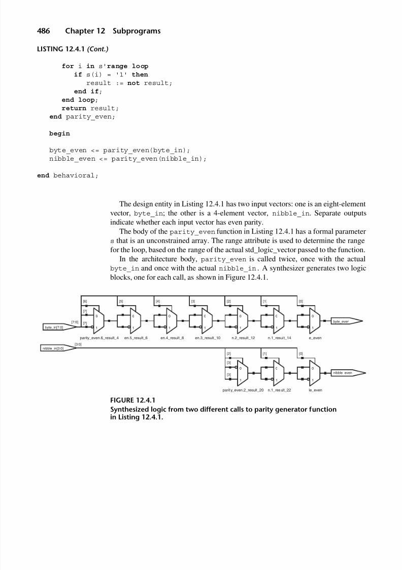
8/9/2019 VHDL for Engineers - Kenneth L. Short.pdf
http://slidepdf.com/reader/full/vhdl-for-engineers-kenneth-l-shortpdf 519/719
486 Chapter 12 Subprograms
LISTING 12.4.1 (Cont.)
for i in s'range loop
if s(i) = '1' then
result := not result;end if;
end loop;return result;
end parity_even;
begin
byte_even <= parity_even(byte_in);nibble_even <= parity_even(nibble_in);
end behavioral;
The design entity in Listing 12.4.1 has two input vectors: one is an eight-elementvector, byte_in; the other is a 4-element vector, nibble_in. Separate outputsindicate whether each input vector has even parity.
The body of the parity_even function in Listing 12.4.1 has a formal parameters that is an unconstrained array. The range attribute is used to determine the rangefor the loop, based on the range of the actual std_logic_vector passed to the function.
In the architecture body, parity_even is called twice, once with the actualbyte_in and once with the actual nibble_in. A synthesizer generates two logicblocks, one for each call, as shown in Figure 12.4.1.
FIGURE 12.4.1
Synthesized logic from two different calls to parity generator functionin Listing 12.4.1.
byte_even
nibble_even
parity_even.6_result_4
parit y_even.2_result_20 n.1_result_22 le_even
en.5_result_6 en.4_result_8 en.3_result_10 n.2_result_12 n.1_result_14
[2]
[3]
[3]
[1] [0]
0
[6]
[7]
[7]
1
[4]
0
1
[5]
0
1
[3]
0
1
[2]
0
1
[1]
0
1byte_in[7:0]
[7:0]
[3:0]nibble_in[3:0]
e_even
[0]
0
1
0
1
0
1
0
1

8/9/2019 VHDL for Engineers - Kenneth L. Short.pdf
http://slidepdf.com/reader/full/vhdl-for-engineers-kenneth-l-shortpdf 520/719
Section 12.4 Array Attributes and Unconstrained Arrays 487
NormalizedUnconstrainedArrays
A subprogram with unconstrained array formal parameters should be written toaccept input arrays not only of any size, but with any index direction. To accomplishthis, the subprogram must be written so that is does not rely on the direction or therange of the actual parameter. This can be accomplished through a technique callednormalization. Using this technique, input arrays are immediately assigned to local
variables whose sizes depend on the sizes of the actual parameters, but that havedescending ranges ending in 0. These variables are then used instead of the formalparameters.
For example, the program in Listing 12.4.2 uses a procedure to compare the magni-tudes of input vectors p and q. Three active-low values are computed by the procedurep_gt_q_bar, p_lt_q_bar, and p_eq_q_bar.
LISTING 12.4.2Magnitude comparison procedure.
library ieee;use ieee.std_logic_1164.all;
entity mag_comp_proc is
port ( p_in : in std_logic_vector (3 downto 0);q_in : in std_logic_vector (0 to 3);p_gt_q_bar, p_eq_q_bar, p_lt_q_bar : out std_logic);
end mag_comp_proc;
architecture behavior of mag_comp_proc is
procedure mag_comp (p : in std_logic_vector; q : in std_logic_vector;signal p_gt_q_bar, p_lt_q_bar, p_eq_q_bar : out std_logic) is
variable p_v : std_logic_vector (p'length - 1 downto 0) := p;variable q_v : std_logic_vector (q'length - 1 downto 0) := q;variable p_gt_q_bar_v, p_lt_q_bar_v, p_eq_q_bar_v : std_logic := '1';
begin
assert p_v'length = q_v'lengthreport "vector parameters must be same length"severity failure;
for i in p_v'range loopif ((p_v(i) = '1') and (q_v(i) = '0')) then
p_gt_q_bar_v := '0';exit;
(Cont.)

8/9/2019 VHDL for Engineers - Kenneth L. Short.pdf
http://slidepdf.com/reader/full/vhdl-for-engineers-kenneth-l-shortpdf 521/719
488 Chapter 12 Subprograms
LISTING 12.4.2 (Cont.)
elsif ((p_v(i) = '0') and (q_v(i) = '1')) then
p_lt_q_bar_v := '0';exit;
end if;end loop;
if ((p_gt_q_bar_v = '1') and (p_lt_q_bar_v = '1')) then
p_eq_q_bar_v := '0';end if;
p_gt_q_bar <= p_gt_q_bar_v;p_lt_q_bar <= p_lt_q_bar_v;p_eq_q_bar <= p_eq_q_bar_v;
end mag_comp ;
begin
mag_comp (p_in, q_in, p_gt_q_bar, p_lt_q_bar, p_eq_q_bar);
end behavior;
The constrained actual parameters passed to the procedure are 4-bit vectors. Oneof these vectors has a descending range and the other has an ascending range. Theprocedure is called by a concurrent procedure call in the architecture body.
The procedure body has two parameters of mode in that are unconstrained arrays,and three parameters that are signals of mode out. The signal parameters of mode outreturn the results. These parameters must be signals, because the procedure is calledusing a concurrent procedure call.
The normalization takes place in the declarative part of the procedure. Two arrayvariables are declared. Each is declared with a length equal to that of its associatedformal parameter by using the length attribute. Each variable is assigned an initialvalue equal to that of its associated formal parameter. As a result, no matter the indexdirection of the actual arrays passed to the procedure, the procedure is written interms of array variables with descending ranges.
In the procedure body an assert statement is used to make sure that the arrayspassed to the procedure are of equal length. If not, an error message is displayedduring simulation. A synthesizer simply ignores the assert statement.
A loop is used to sequence through the elements of the two arrays to determinethe three outputs. This part of the procedure is equivalent to the program inListing 5.7.1.

8/9/2019 VHDL for Engineers - Kenneth L. Short.pdf
http://slidepdf.com/reader/full/vhdl-for-engineers-kenneth-l-shortpdf 522/719
Section 12.4 Array Attributes and Unconstrained Arrays 489
UnconstrainedArray Return Value
An unconstrained array can be used to return an array value from a subprogram. InListing 7.9.1, a process was used to sequentially compute and apply all input combi-nations to a half adder UUT in a testbench. A large number of combinationaltestbenches could use this same kind of stimulus computation. It would be useful if this computation were implemented by a subprogram, so that it could be reused. A
procedure that does this is given in Listing 12.4.3.Procedure binary_stimulus has three formal parameters. Parameter n is an
integer input parameter indicating number of bits in the stimulus (number of UUTinputs to be driven). Parameter p specifies the time between generation of each stimuluscombination. Parameter slv is an unconstrained vector that is the stimulus value.
The procedure uses a loop to produce all possible 2n combinations of n bits. The timebetween each combination is p seconds. Since the function to_unsigned frompackage NUMERIC_STD is used, an appropriate use clause is required in the testbench.
As an example of the use of this procedure, consider a testbench for a UUT withstd_logic inputs a, b, c, and d. A vector is declared in the declarative part of thetestbench to connect the stimulus from procedure binary_stimulus to the UUT:
signal bin_stim : std_logic_vector (3 downto 0);
The statement part of the testbench’s architecture contains the instantiation of theUUT and the following two concurrent statements.
binary_stimulus (4, 20 ns, bin_stim);
(a, b, c, d) <= bin_stim;
The first of these statements is the concurrent call to procedure binary_
stimulus. The actual parameters specify that the stimulus generated is four bitswide, is generated every 20 ns, and is returned as vector bin_stim. The secondconcurrent statement applies vector bin_stim to the aggregate (a, b, c, d).
During simulation initialization the concurrent procedure binary_stimulus isexecuted once. It generates the sixteen stimulus values, each separated by 20 ns, andthen returns.
LISTING 12.4.3Procedure to generate a binary stimulus.
Procedure binary_stimulus (n : integer; p : time ;
signal slv : out std_Logic_vector) isbegin
for i in 0 to 2**n - 1 loop
slv <= std_logic_vector (to_unsigned(i, n)); wait for p;
end loop;end binary_stimulus;

8/9/2019 VHDL for Engineers - Kenneth L. Short.pdf
http://slidepdf.com/reader/full/vhdl-for-engineers-kenneth-l-shortpdf 523/719
490 Chapter 12 Subprograms
Index Rangeof UnconstrainedReturn Values
An unconstrained return value has the index range of the formal parameter used toreturn its value. If the vector returned is assigned in its entirety to an equal lengthvector with a different index range, there is no problem. The assignment is, asalways, made from left to right, independently of the index ranges. However, if anelement from the returned vector is selected directly, it is the index range of the
formal parameter that must be considered in selecting the desired element.This can be a problem when a subprogram is used and an element is selected
directly from a returned vector without knowledge of the index range of the formalparameter used to return its value. In particular, this can be a problem when usingsubprograms from standard packages or de facto standard packages where we havenot examined the subprogram body.
An example to clarify this is given in Listing 12.4.4. This design entity consists of two attempts at selecting bit 0 from the entity’s input vector.
Output outbit_a is bit 0 taken from the input vector, which has a range of 3down to 0. Output outbit_b is bit 0 taken directly from an identity function, whichtakes the input vector as its actual parameter and returns this vector. We wouldexpect these two bit values to be the same because they are both bit 0.
LISTING 12.4.4Design entity to select a bit from a vector.
library ieee;use ieee.std_logic_1164.all;
entity select_bit is
port(
invect : in std_logic_vector(3 downto 0);outbit_a, outbit_b : out std_logic);
end select_bit;
architecture behavioral of select_bit is
function identity (slv : std_logic_vector) return std_logic_vector is
variable lcl_vec : std_logic_vector(0 to slv'length - 1);begin
lcl_vec := slv;return lcl_vec;
end identity;
begin
process (invect)begin
outbit_a <= invect(0); -- selecting bit 0outbit_b <= identity(invect)(0); -- selecting from function_return_value
end process;end behavioral;

8/9/2019 VHDL for Engineers - Kenneth L. Short.pdf
http://slidepdf.com/reader/full/vhdl-for-engineers-kenneth-l-shortpdf 524/719
Section 12.5 Overloading Subprograms and Operators 491
However, the identity function assigns its input vector to a local variable and thislocal variable has a index range increasing from 0. As a result the assignment
outbit_b <= identity(invect)(0);
selects bit 0 of the value returned by the function. This index position is defined bythe local variable used to return the vector, not by the input vector passed to thefunction. Bit 0 is the leftmost bit of the returned vector, not its rightmost bit.
The problem becomes even clearer when the design entity is synthesized. Thesynthesizer realizes that the two outputs are simply the rightmost and leftmostelements of the input vector and synthesizes the “logic” in Figure 12.4.2.
From the schematic of the synthesized logic it is clear that output_a =invect(0) and output_b = invect(3).
12 .5 O VE RL OA DI NG S UBP ROGR AMS A N D O P E R A T O R S
SubprogramOverloading
VHDL allows the same subprogram name to be used for different subprograms. Thisreuse of names is called overloading. Most often overloading is used when the sameor similar operations are to be performed on parameters of different types. We haverepeatedly encountered overloading when using the logical operators on operands of type std_logic. As we will see later in this section, an operator is just a special formof a function.
The logical operators are predefined for type bit and boolean. We have used these
same logical operator names on operands of type std_logic. We are able to do sobecause the functions that overload these logical operator names for operands of type std_logic are provided in package STD_LOGIC_1164.
When a VHDL compiler encounters an overloaded subprogram, it determineswhich of the subprograms with the same name is intended by examining the numberand type of operands used in the subprogram call and, in the case of functions, thereturn type. This process is called operator resolution. As long as each subprogram
FIGURE 12.4.2
Synthesized logic from the code in Listing 12.4.3.
outbit_b
invect[3:0][3:0]
[3]
[0]outbit_a

8/9/2019 VHDL for Engineers - Kenneth L. Short.pdf
http://slidepdf.com/reader/full/vhdl-for-engineers-kenneth-l-shortpdf 525/719
492 Chapter 12 Subprograms
with the same name is unique in these characteristics, the compiler can determinewhich one to use. It is an error if a compiler cannot distinguish between overloadedsubprograms based on these three factors.
Note that it is the base type of parameters that is used in operator resolution. Param-eters of different subtypes that have the same base type are not differentiated. Also, the
class of a parameter is not considered in operator resolution. Two overloaded functionsthat differ in only the class of a parameter cannot be differentiated.
Predefined VHDLOperators
The predefined VHDL operators depend on the type. Table 12.5.1 lists which synthe-sizable types have which predefined operators.
Bit and boolean are special cases of enumeration types. Only the bit and booleantypes have predefined logical operators. Bit and boolean arrays are special cases of thearray type. While the concatenation, equality, and ordering operators are predefined forany one-dimensional array, only bit and boolean one-dimensional arrays have thelogical and shifting operators predefined.
Std_logic is simply an enumeration type. Like all enumeration types, other thanbit and boolean, it has only the equality and ordering operators when it is declared.To add any other operators to std_logic requires operator overloading. This operatoroverloading is provided in package STD_LOGIC_1164.
Array types such as unsigned and signed, declared in package NUMERIC_STD,have the operators concatenation, equality, and ordering predefined as would anyother array type. Logical, shifting, and arithmetic operators for these types areprovided by overloading functions in package NUMERIC_STD.
When we declare a new type of our own, the set of predefined operators for thattype automatically become available. Any other operators that we would like for thisnew type we will have to provide as overloaded functions.
Table 12.5.1Predefined Operators.
Type Arithmetic Logical Concatenation Equality Ordering Shifting
enumeration
bit
boolean
integer
record
array
bit array
boolean array

8/9/2019 VHDL for Engineers - Kenneth L. Short.pdf
http://slidepdf.com/reader/full/vhdl-for-engineers-kenneth-l-shortpdf 526/719
Section 12.5 Overloading Subprograms and Operators 493
LISTING 12.5.1Use of overloaded AND operator for std_logic written in the normal function form.
library ieee;use ieee.std_logic_1164.all;
entity outfix_and isport (x, y: in std_logic; r: out std_logic);
end outfix_and;
architecture function_call of outfix_and is
begin
r <= "and" (x,y);
end function_call;
OperatorOverloading
A common use of functions is to define operators for a type, since operators are justfunctions.
The rules for operator overloading only allow the predefined VHDL operators tobe overloaded. The name of the function is the operator symbol enclosed in quotes.For example, the and operator could be declared as:
function "and" (l, r : bit) return bit;
Because it is a built-in operator, the and function can be called using infix
notation as:
r <= x and y;
or, alternatively, in the normal function call format as:
r <= "and" (x, y);
Note that in this form the operator name is enclosed in double quotes.For example, since the and operator is already overloaded for std_logic operands
in package STD_LOGIC_1164, we can write the and operation in the normal
function form-as shown in Listing 12.5.1.The declaration and body of overloaded subprograms and operators are usually
placed in a package and package body, respectively, so that these subprograms canbe used in multiple design units. Additional examples of operator overloading arepresented in Chapter 13.

8/9/2019 VHDL for Engineers - Kenneth L. Short.pdf
http://slidepdf.com/reader/full/vhdl-for-engineers-kenneth-l-shortpdf 527/719
494 Chapter 12 Subprograms
12 . 6 TY PE C O N V E RS I ON S
A type conversion converts a value from one type to another. VHDL providesexplicit predefined type conversions. Predefined type conversions cannot be
overloaded. User-defined type conversions are also allowed. User-defined typeconversions are written as functions.
Predefined TypeConversions
Predefined type conversions are available to convert from one closely related type toanother. Two types are considered “closely related” if they meet either of the followingconditions:
1. They are both abstract numeric types (integer or floating point).
2. They are both arrays that have the same dimensions, have the same or closelyrelated index types, and have elements that are the same type. Two array types
may be closely related, even if their corresponding index positions have differentdirections.
An explicit predefined type conversion has the form shown in Figure 12.6.1.As the syntax indicates, a predefined type conversion uses the name of the target
type as if it were a function.We have previously used predefined type conversions. For example, in the
counter in Listing 9.4.2 the unsigned signal count_us was used to hold the count.However, the counter’s output port count was type std_logic_vector. Accordingly,we needed to convert from unsigned to std_logic_vector. The assignment statement:
count <= std_logic_vector(count_us);
was used to accomplish this conversion. The type_mark specified is std_logic_
vector. The conversion is possible because the unsigned and std_logic_vectorarrays involved are closely related. They have the same dimensions, the same indextypes, and their elements have the same base type (std_ulogic).
User-Defined TypeConversions
User-defined type conversions are functions that take a value of one type and returna value of another type. Predefined type conversions cannot be overloaded. So,names of types cannot be used to name user-defined type conversion functions. Awidely used convention for naming user-defined type conversion functions is to call
the function to_type, where type is the target type of the conversion.
type_conversion ::=
type_mark ( expression )
FIGURE 12.6.1
Syntax for an explicit type conversion.

8/9/2019 VHDL for Engineers - Kenneth L. Short.pdf
http://slidepdf.com/reader/full/vhdl-for-engineers-kenneth-l-shortpdf 528/719
Section 12.6 Type Conversions 495
Listing 12.6.1Function to convert a natural number to a std_logic_vector.
function to_std_logic_vector(arg: natural; size: positive)return std_logic_vector is
variable result: std_logic_vector (size-1 downto 0);
variable temp: natural;begin
temp := arg;for i in 0 to size-1 loop
if (temp mod 2) = 1 then
result(i) := '1';else
result(i) := '0';end if;
temp := temp / 2;end loop;
return result;end;
For example, assume we needed to convert from subtype natural to std_logic_vector. We cannot use a predefined type conversion, because these two types are notclosely related, because one is a scalar and the other is an array. Accordingly, we musteither find a conversion function in a standard package that accomplishes this, or writeour own function. A user-defined function named to_std_logic_vector is givenin Listing 12.6.1.
This function requires two parameters, the natural number to be converted and the
length of the std_logic_vector to be returned. Following common practice, the typeto be converted is the first parameter and any information required for the conversionis given as subsequent parameters. The conversion algorithm uses a loop to succes-sively divide the natural number by 2. Each division produces one bit of result,starting from the least significant bit.
A mod 2 division is used in the if statement’s condition to determine theremainder after division by 2. This value is assigned to the bit being determined.
If we have a natural number that ranges from 0 to 255, we can convert and assignit to a std_logic_vector of length 8 using the following function call:
std_lg_vect <= to_std_logic_vector(nat_num, 8);
Formal ParameterDefault Values
Formal parameters of a subprogram that are of mode in and class constant can beassigned default values for synthesis. If a default value is included in a parameterspecification, we have the option of omitting the actual value when the subprogramis called. If the actual parameter is at the end of the parameter list, we can simplyomit it. Otherwise, keyword open is used in place of the actual parameter value.

8/9/2019 VHDL for Engineers - Kenneth L. Short.pdf
http://slidepdf.com/reader/full/vhdl-for-engineers-kenneth-l-shortpdf 529/719
496 Chapter 12 Subprograms
LISTING 12.6.2Function using a default parameter.
function to_std_logic_vector(arg: natural; size: positive := 8)return std_logic_vector is
For example, the parameter list for the function in Listing 12.6.1 could be definedusing a default value for the parameter size, as shown in Listing 12.6.2.
The mode for a function parameter is always in and the class defaults to constant.As a result, formal parameter size can be assigned a default value.
The function could then be called as:
std_lg_vect <= to_std_logic_vector(nat_num);
or as:
std_lg_vect <= to_std_logic_vector(nat_num, open);
To convert a natural number to a std_logic_vector that has a dimension other than8, the desired dimension must be specified in the call.
As another example of a conversion function using a default parameter, considerthe function to_bit that converts a std_ulogic value to a bit value. This function isprovided in package STD_LOGIC_1164 and shown in Listing 12.6.3.
This function must map the nine valued std_ulogic type parameter to a two valuedtype bit result. The function maps values '0' and 'L' to '0' and values '1' and'H' to '1'. When the std_ulogic parameter is one of the other five values, a secondformal parameter xmap with the default assignment of '0' is used to map these
values. The value of xmap is returned as the result when the std_ulogic value to beconverted is other than '0', 'L', '1', or 'H'. If we want these five values to bemapped to zero, we can call the function with a single parameter. However, if wewould like these other five values mapped to '1' instead, we call the function with'1' specified as the second parameter.
LISTING 12.6.3To_bit conversion function using a default parameter.
function to_bit ( s : std_ulogic; xmap : bit := '0') return bit is
begincase s is
when '0' | 'L' => return ('0'); when '1' | 'H' => return ('1'); when others => return xmap;end case;
end;

8/9/2019 VHDL for Engineers - Kenneth L. Short.pdf
http://slidepdf.com/reader/full/vhdl-for-engineers-kenneth-l-shortpdf 530/719
Section 12.6 Type Conversions 497
LISTING 12.6.4Function to convert a std_logic type to a character type.
function chr(sl: std_logic) return character is
variable c: character;begin
case sl is when 'U' => c:= 'U'; when 'X' => c:= 'X'; when '0' => c:= '0'; when '1' => c:= '1'; when 'Z' => c:= 'Z'; when 'W' => c:= 'W'; when 'L' => c:= 'L'; when 'H' => c:= 'H'; when '-' => c:= '-';
end case;
return c;end chr;
Conversion of aStd_logic_vectorto a String
Another useful example of a type conversion is the conversion of a std_logic_vector value to a string. For example, such a function can be used to display thevalue of a std_logic_vector in an assert or report statement. This conversion can beaccomplished using two functions. The first function, chr, converts a singlestd_logic value to the corresponding character type value. This function is given inListing 12.6.4.
The formal parameter’s type for this function is std_logic. The function’s return
type is character. The function declares a variable c of type character. A casestatement uses an expression that is the value of the std_logic parameter passed tothe function. Each branch of the case has a choice, which is one of the nine std_logicvalues. The branch whose choice corresponds to the value of the parameter passed tothe function assigns the character variable c the corresponding character type value.The return statement returns the value of the variable.
The second function, str, converts a std_logic_vector to a string using thefunction chr. Function str is given in Listing 12.6.5.
A string variable is declared to hold the result. Since the index range for a stringis type positive, the index for this variable ranges from 1 to the length of thestd_logic_vector passed to the function. An integer variable is also declared for use
as the string index.The conversion is accomplished in a loop. Each time through the loop one
element of the std_logic_vector is converted to a character by calling the chr
function. Note that the loop index cannot also be used to index the element of result, because they may have different ranges. After the loop terminates, the stringvariable’s value is returned by the function.

8/9/2019 VHDL for Engineers - Kenneth L. Short.pdf
http://slidepdf.com/reader/full/vhdl-for-engineers-kenneth-l-shortpdf 531/719
498 Chapter 12 Subprograms
LISTING 12.6.5Function to convert a std_logic_vector to a string.
function str(slv: std_logic_vector) return string is
variable result : string (1 to slv'length);variable r : integer;
beginr := 1;for i in slv'range loop
result(r) := chr(slv(i));r := r + 1;
end loop;return result;
end str;
If these two functions are declared in the architecture of a testbench, the reportclause of an assert statement can be used to display a message that gives the stimulusvalue that causes an assertion violation. For example, if the stimulus is a std_logic_vector named input, the report statement
report "Output incorrect for input of " & str(input)
displays the value of input as a string of 0s and 1s.Since these two functions would find widespread use in testbenches, it is more
convenient to place them in a package in a library. They would then be availablefor use in any testbench, as long as the appropriate library and use clauses wereincluded.
PROBLE MS
12.1 List the basic similarities and differences between a function and a procedure in VHDL.
12.2 Write a program that implements the D latch in Figure 12.1.1 using only the functionnand_2f and local signals.
12.3 Write a program that implements the D latch in Figure 12.1.1 using only the procedurenand_2p and local signals.
12.4 What is meant by the class of a formal parameter? What are the possible classes for the formalparameters of a function? What is the default class of a formal parameter of a function? Whatis meant by the mode of a formal parameter? What are the possible modes for the formalparameters of a function? What is the default mode of a formal parameter for a function?
12.5 What are the differences between variables declared in a function and variables declared in aprocess?
12.6 Write a function named nand_fcn that returns the result of an eight-input NAND operationon its inputs. The function’s parameters are all type std_logic. If the function is called withfewer than eight actual input parameters the other unused inputs default to '1's. As a result,

8/9/2019 VHDL for Engineers - Kenneth L. Short.pdf
http://slidepdf.com/reader/full/vhdl-for-engineers-kenneth-l-shortpdf 532/719
Problems 499
this function can be used to implement a NAND gate with one to eight inputs. What could aone-input NAND gate be?
12.7 A two-wide two-input AND-OR-INVERT gate consists of two 2-input AND gates whoseoutputs are ORed together and the result inverted. Write a function a0i_2w_2i thatimplements an equivalent operation.
12.8 What are the possible classes for the formal parameters of a procedure? What are the possiblemodes for the formal parameters of a procedure? What is the default class of a formalparameter of a procedure that is mode out?
12.9 Write a procedurenorproc that implements a two-input NOR gate. Draw a logic diagram of a S-R (set–reset) latch consisting of cross-coupled NOR gates. Write a VHDL description of aS-R latch. The architecture for this latch must be based on concurrent calls to the procedurenorproc.
12.10 A function named ones_count has a single formal parameter that is an unconstrainedstd_logic_vector. The function returns an integer. The integer specifies the number of elementsthat are 1s in the actual vector passed to the function. Write the function.
Write a design description of a five-input majority voting circuit. This circuit uses the functionones_count. The five-input majority voting circuit has the following entity declaration:
entity majority isport(
voters : in std_logic_vector(4 downto 0);maj : out std_logic;
end majority;
Output maj is a '1' whenever the majority (more than half) of the bits of voters are '1's.
12.11 An entity named reorder has an 8-bit std_logic_vector input and an 8-bit std_logic_vectoroutput. The bits of the entity’s output vector have the reverse order of the bits of its input vector.Write a description of the design entity. The description must use a single concurrent call to afunction to implement the entity. The function is defined in the declaration region of thearchitecture body. The function, named reorder_vec, returns a std_logic vector whose bitshave the reverse order of the bits in the std_logic_vector passed to the function. The functionreorder_vec must be written to handle a vector of any length. Draw a diagram of the circuitthat would be synthesized from this description.
12.12 Write a description of a system that determines whether two 8-bit std_logic_vector inputs are botheven or both odd parity. The entity’s name is parity_comp. The input vectors are x andy. Theoutput is the std_logic signal same_par. Signal same_par is a '1' if both input vectors areeven parity or both are odd parity; otherwise, it is a '0'. Use the function parity_even fromListing 12.2.1 in this design.
12.13 The function to_integer, which converts a std_logic_vector to an integer, has the followingdeclaration:
function to_integer (slv: in std_logic_vector) return natural;
Use the function to_integer to write a function that overloads the + operator to add twostd_logic_vectors. Assume the two vectors to be added and their sum are all the same length.The carry from the addition is discarded.

8/9/2019 VHDL for Engineers - Kenneth L. Short.pdf
http://slidepdf.com/reader/full/vhdl-for-engineers-kenneth-l-shortpdf 533/719
500 Chapter 12 Subprograms
12.14 The VHDL code for a procedure is to be written. This procedure is similar in purpose to thefunction to_integer, whose declaration was given in Problem 12.13. The procedure’sdeclaration is:
procedure vector_to_int (slv : in std_logic_vector; x_flag :out boolean; q : inout integer);
The procedure converts the std_logic_vector slv to an integer and returns the integer value asq. However, if any element of the vector is other than a '0' or a '1', thenx_flag is returnedtrue to indicate this condition.

8/9/2019 VHDL for Engineers - Kenneth L. Short.pdf
http://slidepdf.com/reader/full/vhdl-for-engineers-kenneth-l-shortpdf 534/719
501
Chapter 13
Packages
In Chapter 12 we saw how subprograms are used to advantage in designs. As designsbecome more complex and more subprograms are used, placement of subprogramdeclarations or bodies in the declarative part of an architecture body or a process canmake the overall form of the program less clear. In addition, to reuse these subpro-grams in other design units requires that their code be duplicated. Subprograms arenot design units, so they cannot be placed alone in a separate file and compiled.
In VHDL, a package is used to collect together related commonly used declara-tions, so that they can easily be made visible for use by multiple design units. Thesedeclarations include constants, types, functions, and procedures. Since a package is adesign unit, it can be placed alone in a separate file and compiled.
Commonly used subprograms for type conversion, resolution of multiply drivensignals, and overloading operators are usually placed in packages. Packages mayalso contain definitions of constants and additional types. Packages are typicallyplaced in libraries. We have previously used types and functions provided inpackages in the IEEE library.
Use of subprograms available in standard packages saves time and is preferable towriting our own equivalent subprograms.
1 3. 1 P AC KA GE S A ND PA CK AG E B OD IE S
A subprogram can be defined locally (within an architecture or process). Its usage isthen limited to that architecture or process. The only way a subprogram can be madeavailable to multiple design units is for it to be declared in a package. Thesubprogram is then also readily available for reuse in later designs.
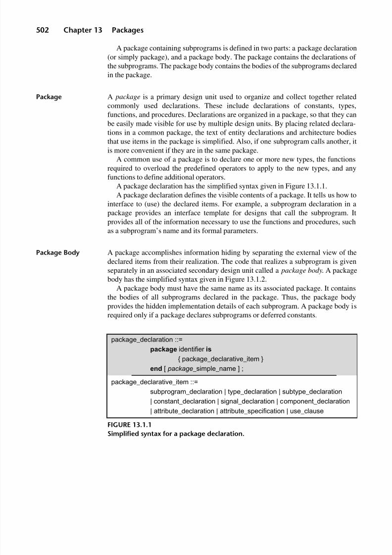
8/9/2019 VHDL for Engineers - Kenneth L. Short.pdf
http://slidepdf.com/reader/full/vhdl-for-engineers-kenneth-l-shortpdf 535/719
502 Chapter 13 Packages
A package containing subprograms is defined in two parts: a package declaration(or simply package), and a package body. The package contains the declarations of the subprograms. The package body contains the bodies of the subprograms declaredin the package.
Package A package is a primary design unit used to organize and collect together relatedcommonly used declarations. These include declarations of constants, types,functions, and procedures. Declarations are organized in a package, so that they canbe easily made visible for use by multiple design units. By placing related declara-tions in a common package, the text of entity declarations and architecture bodiesthat use items in the package is simplified. Also, if one subprogram calls another, itis more convenient if they are in the same package.
A common use of a package is to declare one or more new types, the functionsrequired to overload the predefined operators to apply to the new types, and anyfunctions to define additional operators.
A package declaration has the simplified syntax given in Figure 13.1.1.A package declaration defines the visible contents of a package. It tells us how to
interface to (use) the declared items. For example, a subprogram declaration in apackage provides an interface template for designs that call the subprogram. Itprovides all of the information necessary to use the functions and procedures, suchas a subprogram’s name and its formal parameters.
Package Body A package accomplishes information hiding by separating the external view of thedeclared items from their realization. The code that realizes a subprogram is givenseparately in an associated secondary design unit called a package body. A package
body has the simplified syntax given in Figure 13.1.2.A package body must have the same name as its associated package. It contains
the bodies of all subprograms declared in the package. Thus, the package bodyprovides the hidden implementation details of each subprogram. A package body isrequired only if a package declares subprograms or deferred constants.
package_declaration ::=
package identifier is
{ package_declarative_item }
end [ package _simple_name ] ;
package_declarative_item ::=
subprogram_declaration | type_declaration | subtype_declaration
| constant_declaration | signal_declaration | component_declaration
| attribute_declaration | attribute_specification | use_clause
FIGURE 13.1.1
Simplified syntax for a package declaration.

8/9/2019 VHDL for Engineers - Kenneth L. Short.pdf
http://slidepdf.com/reader/full/vhdl-for-engineers-kenneth-l-shortpdf 536/719
Section 13.1 Packages and Package Bodies 503
A subprogram body in a package body must have a subprogram declarationportion that is exactly as written in the package declaration. That is, the names,
types, modes, and default values of each formal parameter must be repeated exactly.
Package slv_str Functions chr and str (see “Conversion of a Std_logic_vector to a String” onpage 560) can be placed in a package and compiled to a library. Listing 13.1.1 showsa package and package body containing these two functions. Any design with acontext clause referencing the library and the package slv_str can call thesefunctions.
LISTING 13.1.1A package and package body containing two functions.
library ieee;use ieee.std_logic_1164.all;
package slv_str is
function chr(sl: std_logic) return character;function str(slv: std_logic_vector) return string;
end slv_str;
package body slv_str is
function chr(sl: std_logic) return character is
variable c: character;begin
case sl is
when 'U' => c:= 'U'; when 'X' => c:= 'X'; when '0' => c:= '0'; when '1' => c:= '1';
(Cont.)
package_body ::=
package body package _simple_name is
{ package_body_declarative_item }
end [ package _simple_name ] ;
package_body_declarative_item ::=subprogram_declaration | subprogram_body | type_declaration
| subtype_declaration | constant_declaration | shared _variable_declaration
| file_declaration | alias_declaration | use_clause | group_template_declaration
| group_declaration
FIGURE 13.1.2
Syntax for a package body.
8/9/2019 VHDL for Engineers - Kenneth L. Short.pdf
http://slidepdf.com/reader/full/vhdl-for-engineers-kenneth-l-shortpdf 537/719
504 Chapter 13 Packages
LISTING 13.1.1 (Cont.)
when 'Z' => c:= 'Z'; when 'W' => c:= 'W'; when 'L' => c:= 'L'; when 'H' => c:= 'H'; when '-' => c:= '-';
end case;return c;
end chr;
function str(slv: std_logic_vector) return string is
variable result : string (1 to slv'length);variable r : integer;
begin
r := 1;for i in slv'range loop
result(r) := chr(slv(i));r := r + 1;
end loop;return result;
end str;
end slv_str;
If desired, the package and package body can be placed in separate files andcompiled separately. In that case, the file containing the package must be compiled
before the file containing the package body.
Deferred Constants When a constant is declared in a package, its name and type must be specified.However, the assignment of a value to the constant can be done either as part of itsdeclaration in the package, or it can be deferred to the package body. If the assignmentof a value to a constant is done in the package, the constant is a fully specified
constant . In contrast, if the assignment is deferred to the package body, the constant isa deferred constant . A deferred constant’s declaration in the package is repeated in thepackage body, along with the addition of the initialization expression for the constant’svalue.
If a package declares only types, signals, or fully specified constants, noassociated package body is necessary.
Declarations in aPackage Body
In addition to the bodies of any subprograms or deferred constants declared in apackage, a package body may contain full declarations of additional types, subtypes,constants, and subprograms used in the package body to realize the subprogramsdeclared in the package. These items are not visible outside of the package body.

8/9/2019 VHDL for Engineers - Kenneth L. Short.pdf
http://slidepdf.com/reader/full/vhdl-for-engineers-kenneth-l-shortpdf 538/719
Section 13.2 Standard and De facto Standard Packages 505
Global Signals A package body cannot declare any signals. Signals may only be declared in apackage. Signals declared in a package are global signals. They are visible anywherethe package is used.
Packages
in Libraries
Packages and package bodies are compiled to libraries. They may be compiled to the
working library or to a resource library. Usually, a package is compiled into theworking library (work) by default. However, packages that are of general use aretypically compiled to a resource library. Different VHDL compilers use differentways to specify into which library a package is compiled. These procedures aredelineated in the compiler’s documentation.
The order of compilation of packages and package bodies is important. Since apackage body depends on information defined in its associated package, the packagemust be compiled before its package body. A package must also be compiled beforean entity declaration or architecture body that uses any items declared in thepackage.
A more complete discussion of libraries and the compilation of design units isgiven in Sections 15.2 and 15.3.
13 . 2 S T AN D AR D A N D DE FA C TO S T A N D A R D P A C K A G E S
As we have seen, the predefined types, operators, and functions declared in packagesSTANDARD and TEXTIO from the library STD are not sufficient for our simulationand synthesis needs. VHDL allows us to define our own data types and operators and
place them in packages so that we can use them in our designs.However, most of the data types and operators that we normally need are already
available in IEEE standard packages and in de facto standard packages commonlyincluded in the IEEE library provided by tool vendors with their simulation orsynthesis tools. Use of these standard packages or de facto standard packages savesus the time required to develop our own packages and improves code portability.Another advantage is that many tool vendors provide optimized implementations of these packages.
Some of these packages are listed in Table 13.2.1. Listed first are the predefinedpackages STANDARD and TEXTIO. Packages STD_LOGIC_1164, NUMERIC_BIT,
and NUMERIC_STD are defined by IEEE standards and included in the IEEE Library.Although packages STD_LOGIC_UNSIGNED, STD_LOGIC_SIGNED, and STD_LOGIC_ARITH are usually included by tool vendors in their IEEE libraries, they arenot actually IEEE standards. However, because of their widespread use, they are defacto standards.
This section provides a brief overview of these packages. Later sections of thischapter provide a more detailed look at some of these packages, to provide thebackground necessary to allow the actual source code of these packages to be read

8/9/2019 VHDL for Engineers - Kenneth L. Short.pdf
http://slidepdf.com/reader/full/vhdl-for-engineers-kenneth-l-shortpdf 539/719
506 Chapter 13 Packages
and understood and to provide further examples of how subprograms are written.The source code is contained in the actual standards documents for those packages
that are IEEE standards. Tool vendors sometimes supply the source code with theirIEEE library.Tool vendors are not allowed to add declarations to or delete declarations from
packages that are IEEE standards. However, they are allowed to modify the packagebodies to create more efficient implementations. Any modified package body mustbe semantically identical to the original package body in the standard.
PackageSTANDARD
VHDL compilers come with a library called Std. Library Std is predefined by theVHDL 1076 standard. This library contains two packages: STANDARD andTEXTIO. It is in package STANDARD that the predefined types and operators of VHDL are declared. For example, type bit and the and operator.
Because almost every VHDL description needs to use types and operators frompackage STANDARD, its contents are automatically made visible to all design units.
Package TEXTIO Package TEXTIO contains predefined types, functions, and procedures used forreading and writing files.
PackageSTD_LOGIC_1164
Type std_ulogic and subtype std_logic, along with their corresponding vector typesstd_ulogic_vector and std_logic_vector, are defined in package STD_LOGIC_1164.
The basic logical operators (and, or, not, and so on) are overloaded for thesetypes in this package.
PackageNUMERIC_STD
Std_logic_vector, as defined in package STD_LOGIC_1164, is not a numeric repre-sentation. However, it can be interpreted as representing an array of logic values, anunsigned value, or a signed value. To treat std_logic_vector as a numeric value, arith-metic operators such as addition, subtraction, and inequality would have to bedefined by the user, and their functions written. Many of these functions would have
Table 13.2.1Standard packages commonly used in synthesis.
Packages Library Standard Number Standard Title
standard, textio std IEEE Std 1076 IEEE Standard VHDL Language Reference
Manualstd_logic_1164 ieee IEEE Std 1164 IEEE Standard Multivalue Logic System
for VHDL Model Interoperability(Std_logic_1164)
numeric_bit, numeric_std ieee IEEE Std 1076.3 IEEE Standard VHDL Synthesis Packages
std_logic_unsigned, std_logic_signed ieee None None
std_logic_arith ieee None None

8/9/2019 VHDL for Engineers - Kenneth L. Short.pdf
http://slidepdf.com/reader/full/vhdl-for-engineers-kenneth-l-shortpdf 540/719
Section 13.2 Standard and De facto Standard Packages 507
to differ, depending on whether a std_logic_vector was to be interpreted as anunsigned or signed value.
To avoid confusion as to how a std_logic_vector is to be interpreted, separatetypes can be created. IEEE Std 1076.3 provides two packages for this purpose:NUMERIC_STD and NUMERIC_BIT. NUMERIC_STD defines two vector types
whose elements are type std_logic. These two types are named unsigned and signed because they represent unsigned and signed numeric values, respectively. Therelated arithmetic operators are also defined in this package.
Package NUMERIC_STD provides essentially the same functionality as anearlier package named STD_LOGIC_ARITH. Package STD_LOGIC_ARITH wasdeveloped by EDA tool vendor Synopsys. Although the Synopsys package isprovided by most VHDL tool vendors in their implementations of the IEEE library,it is proprietary and not a standard. In fact, package NUMERIC_STD was developedby the IEEE so that there would be a nonproprietary standard numeric packageavailable that could be adopted by all tool vendors.
Package NUMERIC_STD has significantly fewer conversion functions thanpackage STD_LOGIC_ARITH. Instead, many type conversions are done using theinherent type conversion capability of the VHDL language.
PackageNUMERIC_BIT
Package NUMERIC_BIT also defines two vector types, also named unsigned andsigned. However, their elements are type bit, rather than std_logic.
PackagesSTD_LOGIC_UNSIGNED and
STD_LOGIC_SIGNED
Originally, Synopsys developed two packages, STD_LOGIC_UNSIGNED andSTD_LOGIC_SIGNED, that provide arithmetic, conversion, and comparison for typestd_logic_vector. These separate packages interpret std_logic_vector as either unsignedor signed, respectively. Package STD_LOGIC_UNSIGNED performs unsigned arith-metic on std_logic types and returns std_logic types. Package STD_LOGIC_SIGNEDperforms signed arithmetic on std_logic types and returns std_logic types.
A drawback of these packages is that we can only use one or the other in a design.Therefore, our design would have to deal with either unsigned or signedstd_logic_vector numbers exclusively. This presented a problem in designs thatneeded to deal with both unsigned and signed numbers.
Package
STD_LOGIC_ARITH
Synopsys later developed package STD_LOGIC_ARITH. This package allows
use of both unsigned and signed interpretations of std_logic_vectors in a singledesign.Package STD_LOGIC_ARITH declares two types, unsigned and signed, that are
vectors of std_logic elements. In this way, the arithmetic operators for these two typesare defined appropriately. Arithmetic comparison functions between unsigned andsigned and conversion functions between unsigned, signed, or std_logic_vector arealso provided.
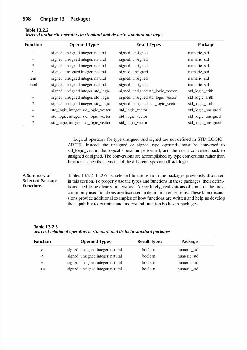
8/9/2019 VHDL for Engineers - Kenneth L. Short.pdf
http://slidepdf.com/reader/full/vhdl-for-engineers-kenneth-l-shortpdf 541/719
508 Chapter 13 Packages
Logical operators for type unsigned and signed are not defined in STD_LOGIC_ARITH. Instead, the unsigned or signed type operands must be converted tostd_logic_vector, the logical operation performed, and the result converted back tounsigned or signed. The conversions are accomplished by type conversions rather thanfunctions, since the elements of the different types are all std_logic.
A Summary ofSelected PackageFunctions
Tables 13.2.2–13.2.6 list selected functions from the packages previously discussedin this section. To properly use the types and functions in these packages, their defini-tions need to be clearly understood. Accordingly, realizations of some of the mostcommonly used functions are discussed in detail in later sections. These later discus-sions provide additional examples of how functions are written and help us developthe capability to examine and understand function bodies in packages.
Table 13.2.3Selected relational operators in standard and de facto standard packages.
Table 13.2.2Selected arithmetic operators in standard and de facto standard packages.
Function Operand Types Result Types Package
+ signed, unsigned integer, natural signed, unsigned numeric_std
– signed, unsigned integer, natural signed, unsigned numeric_std* signed, unsigned integer, natural signed, unsigned numeric_std
/ signed, unsigned integer, natural signed, unsigned numeric_std
rem signed, unsigned integer, natural signed, unsigned numeric_std
mod signed, unsigned integer, natural signed, unsigned numeric_std
+ signed, unsigned integer, std_logic signed, unsigned std_logic_vector std_logic_arith
– signed, unsigned integer, std_logic signed, unsigned std_logic_vector std_logic_arith
* signed, unsigned integer, std_logic signed, unsigned, std_logic_vector std_logic_arith
+ std_logic, integer, std_logic_vector std_logic_vector std_logic_unsigned
– std_logic, integer, std_logic_vector std_logic_vector std_logic_unsigned* std_logic, integer, std_logic_vector std_logic_vector std_logic_unsigned
Function Operand Types Result Types Package
> signed, unsigned integer, natural boolean numeric_std
< signed, unsigned integer, natural boolean numeric_std
= signed, unsigned integer, natural boolean numeric_std
>= signed, unsigned integer, natural boolean numeric_std

8/9/2019 VHDL for Engineers - Kenneth L. Short.pdf
http://slidepdf.com/reader/full/vhdl-for-engineers-kenneth-l-shortpdf 542/719
Section 13.2 Standard and De facto Standard Packages 509
<= signed, unsigned integer, natural boolean numeric_std
/= signed, unsigned integer, natural boolean numeric_std
> signed, unsigned integer boolean std_logic_arith
< signed, unsigned integer boolean std_logic_arith
= signed, unsigned integer boolean std_logic_arith
>= signed, unsigned integer boolean std_logic_arith
<= signed, unsigned integer boolean std_logic_arith
/= signed, unsigned integer boolean std_logic_arith
> std_logic_vector, integer std_logic_vector std_logic_unsigned
< std_logic_vector, integer std_logic_vector std_logic_unsigned
= std_logic_vector, integer std_logic_vector std_logic_unsigned
>= std_logic_vector, integer std_logic_vector std_logic_unsigned
<= std_logic_vector, integer std_logic_vector std_logic_unsigned /= std_logic_vector, integer std_logic_vector std_logic_unsigned
Function Operand Types Result Types Package
Table 13.2.4Selected shift operators in standard and de facto standard packages.
Function Operand Types Result Types Package
shift_left signed, unsigned, natural signed, unsigned numeric_std
shift_right signed, unsigned, natural signed, unsigned numeric_std
rotate_left signed, unsigned, natural signed, unsigned numeric_std
rotate_right signed, unsigned, natural signed, unsigned numeric_std
sll signed, unsigned, integer signed, unsigned numeric_std
srl signed, unsigned, integer signed, unsigned numeric_std
rol signed, unsigned, integer signed, unsigned numeric_stdror signed, unsigned, integer signed, unsigned numeric_std
shl signed, unsigned integer signed, unsigned std_logic_arith
shr signed, unsigned integer signed, unsigned std_logic_arith
shl std_logic_vector, integer std_logic_vector std_logic_unsigned
shr std_logic_vector, integer std_logic_vector std_logic_unsigned

8/9/2019 VHDL for Engineers - Kenneth L. Short.pdf
http://slidepdf.com/reader/full/vhdl-for-engineers-kenneth-l-shortpdf 543/719
510 Chapter 13 Packages
13 .3 PA CK AG E STD _LO GIC _1 164
To eliminate portability problems resulting from the use of nonstandard multivaluedlogic types, IEEE Std 1164 was developed and was ratified by the IEEE in 1993.This standard contains package STD_LOGIC_1164, which defines types, subtypes,and functions to extend VHDL by adding a nine-value data type called std_ulogic.Package STD_LOGIC_1164 is also called the standard logic value package, or MVL9 (for multivalued logic, nine values). All VHDL tool vendors support thisstandard. Std_logic, a subtype of std_ulogic, was introduced in Section 3.4 and hasbeen used extensively throughout this book.
ResolutionFunction forStd_logic
As previously discussed, std_logic is a resolved type. Since a resolved signal canhave multiple sources, its declaration must also include a resolution function. Theresolution function determines the resultant signal value from the values of a signal’s
Table 13.2.5Selected type conversion functions in standard and de facto standard packages.
Function Operand Types Result Types Package
to_integer signed, unsigned integer, natural numeric_std
to_unsigned std_logic_vector, natural unsigned numeric_stdto_signed std_logic_vector, natural signed numeric_std
conv_integer signed, unsigned std_ulogic, integer integer std_logic_arith
conv_signed signed, unsigned std_ulogic, integer signed std_logic_arith
conv_unsigned signed, unsigned std_ulogic, integer unsigned std_logic_arith
conv_std_logic_vector signed, unsigned std_ulogic, integer std_logic_vector std_logic_arith
conv_integer std_logic_vector integer std_logic_unsigned
Table 13.2.6Selected miscellaneous functions in standard and de facto standard packages.
Function Operand Types Result Types Package
resize singed, unsigned, natural signed, unsigned numeric_std
std_match signed, unsigned, std_logic_vector, std_ulogic_vector boolean numeric_std
ext std_logic_vector std_logic_vector std_logic_arith
sxt std_logic_vector std_logic_vector std_logic_arith
abs signed signed std_logic_arith

8/9/2019 VHDL for Engineers - Kenneth L. Short.pdf
http://slidepdf.com/reader/full/vhdl-for-engineers-kenneth-l-shortpdf 544/719
Section 13.3 Package STD_LOGIC_1164 511
multiple sources. Package STD_LOGIC_1164 contains the declaration of aresolution function name resolved. The function’s declaration is:
function resolved ( s : std_ulogic_vector ) return std_ulogic;
The function’s body, as defined in package body STD_LOGIC_1164, is shown inListing 13.3.1.Type stdlogic_table is declared as:
type stdlogic_table is array(std_ulogic, std_ulogic) of std_ulogic;
LISTING 13.3.1The resolution function resolved as defined in package body STD_LOGIC_1164.
type stdlogic_table is array(std_ulogic, std_ulogic) of std_ulogic;
constant resolution_table : stdlogic_table := (-- ----------------------------------------------------------- | U X 0 1 Z W L H - | |-- ---------------------------------------------------------
( 'U', 'U', 'U', 'U', 'U', 'U', 'U', 'U', 'U' ), -- | U |( 'U', 'X', 'X', 'X', 'X', 'X', 'X', 'X', 'X' ), -- | X |( 'U', 'X', '0', 'X', '0', '0', '0', '0', 'X' ), -- | 0 |( 'U', 'X', 'X', '1', '1', '1', '1', '1', 'X' ), -- | 1 |( 'U', 'X', '0', '1', 'Z', 'W', 'L', 'H', 'X' ), -- | Z |( 'U', 'X', '0', '1', 'W', 'W', 'W', 'W', 'X' ), -- | W |( 'U', 'X', '0', '1', 'L', 'W', 'L', 'W', 'X' ), -- | L |( 'U', 'X', '0', '1', 'H', 'W', 'W', 'H', 'X' ), --
| H |( 'U', 'X', 'X', 'X', 'X', 'X', 'X', 'X', 'X' ) -- | - |);
function resolved ( s : std_ulogic_vector ) return std_ulogic is
variable result : std_ulogic := 'z'; -- weakest state defaultbegin
-- the test for a single driver is essential otherwise the-- loop would return 'x' for a single driver of '-' and that-- would conflict with the value of a single driver unresolved -- signal.if (s'length = 1) then return s(s'low);
elsefor i in s'range loop
result := resolution_table(result, s(i));end loop;
end if;return result;
end resolved

8/9/2019 VHDL for Engineers - Kenneth L. Short.pdf
http://slidepdf.com/reader/full/vhdl-for-engineers-kenneth-l-shortpdf 545/719
512 Chapter 13 Packages
This statement declares a two-dimensional array of type std_ulogic. The range of each of the array’s dimension is the enumerated range of type std_ulogic, or ('U','X', '0', '1', 'Z', 'W', 'L', 'H', '-').
Constant resolution_table is then defined. Its type is the previously definedtwo-dimensional array of type std_ulogic named stdlogic_table. This table of
constants concisely defines the rules for resolving a multiply driven std_logic signal. Theentries in the table must define a commutative function, so that the values may be passedto the function in any order. The commutative nature of the table entries is apparentbecause entry values are reflected along a diagonal from the top left to the bottom right.
Unlike other functions we have considered, we never write a call to a resolutionfunction. Instead, the function is automatically called by the simulator each time atransaction is executed for a driver of a multiply driven std_logic signal. Functionresolved takes as its parameter a single unconstrained std_ulogic_vector arraycreated and passed to it by the simulator. The simulator uses the new driver trans-action value and the values of any other drivers of the signal to form the array that itpasses to the function resolved. The result returned by resolved is the new valueof the multiply driven signal.
When called, resolved first initializes the variable result to the value 'Z'.The if statement then uses the length attribute to check whether the length of thearray passed to the function is 1. If this is the case, the signal has a single driver andits resolved value is the value of that single driver. The low attribute returns thelower bound of the index range of the array passed to the function. So, s(s'low) issimply the sole element of the one element array that was passed to the function.
If the length of the array passed is greater than 1, a loop is entered. This loop takesthe loop index i through all the values in the range of the array. Each time through theloop, the value of result is used as the row index into resolution_table and the
value of array element i is used as the column index. The table entry at this row andcolumn becomes the new value of result. When the loop is completed, the value of result is the resolved value of all the elements of the array passed to the function.The value of result is then returned by the function.
Std_ulogicSubtypes WithoutStrength: X01,X01Z, UX01, UX01Z
Package STD_LOGIC_1164 includes the declaration of four additional subtypesthat exclude weak strength values. These subtypes are used by functions in thepackage. Each subtype’s name is an acronym formed by the values included in thesubtype. Their declarations are:
subtype X01 is resolved std_ulogic range 'X' to '1';-- ('X','0','1')subtype X01Z is resolved std_ulogic range 'X' to 'Z';-- ('X','0','1','Z')subtype UX01 is resolved std_ulogic range 'U' to '1';-- ('U','X','0','1')subtype UX01Z is resolved std_ulogic range 'U' to 'Z';-- ('U','X','0','1','Z')

8/9/2019 VHDL for Engineers - Kenneth L. Short.pdf
http://slidepdf.com/reader/full/vhdl-for-engineers-kenneth-l-shortpdf 546/719
Section 13.3 Package STD_LOGIC_1164 513
The range of these subtypes is specified in terms of the ordered enumeration thatdefines std_ulogic. Therefore, range 'X' to '1' starts with 'X', includes '0',and ends with '1'.
None of these subtypes includes any of the values that represent weak signals:'W', 'L', 'H'. These subtypes are useful when we don’t care about the strength of a
signal, only its logical value.Each of these subtypes is also a closed subtype. This means that the result of
resolving values of the subtype is a value of the subtype.
Overloaded LogicalOperators forStd_logic
Recall that the logical operators defined in IEEE Std 1076 for bit and boolean typesare overloaded in package STD_LOGIC_1164 for std_logic. The functions thatdefine these overloaded operators also use table lookups. The tables and functionsare declared in the STD_LOGIC_1164 package and the functions are realized in theSTD_LOGIC_1164 package body. For example, the table for the and function isgiven in Listing 13.3.2
The entries in the table are restricted to values of subtype UX01. Thus, the resultof a table lookup for the and operation is a value of subtype UX01.
The and function for std_ulogic types, as given the in the package body, is:
function "and" ( l : std_ulogic; r : std_ulogic )return UX01 is
begin
return (and_table(l, r));end "and";
In the function body, the name of the function is placed in quotes, ("and"). These
quotes indicate that the name is that of one of the predefined operators. The param-eters are denoted l and r to indicate that these are the operands to the left and right
LISTING 13.3.2Table of constants used to overload the AND function for std_logic.
constant and_table : stdlogic_table := (-- ------------------------------------------------------ | U X 0 1 Z W L H - | |-- ----------------------------------------------------
( 'U', 'U', '0', 'U', 'U', 'U', '0', 'U', 'U' ), -- | U |( 'U', 'X', '0', 'X', 'X', 'X', '0', 'X', 'X' ), -- | X |
( '0', '0', '0', '0', '0', '0', '0', '0', '0' ), -- | 0 |( 'U', 'X', '0', '1', 'X', 'X', '0', '1', 'X' ), -- | 1 |( 'U', 'X', '0', 'X', 'X', 'X', '0', 'X', 'X' ), -- | Z |( 'U', 'X', '0', 'X', 'X', 'X', '0', 'X', 'X' ), -- | W |( '0', '0', '0', '0', '0', '0', '0', '0', '0' ), -- | L |( 'U', 'X', '0', '1', 'X', 'X', '0', '1', 'X' ), -- | H |( 'U', 'X', '0', 'X', 'X', 'X', '0', 'X', 'X' ) -- | - |
);

8/9/2019 VHDL for Engineers - Kenneth L. Short.pdf
http://slidepdf.com/reader/full/vhdl-for-engineers-kenneth-l-shortpdf 547/719
514 Chapter 13 Packages
of the operator, respectively. The return value is indicated to be of subtype UX01. Theand function returns the value obtained from the table lookup using tableand_table with l as the row index and r as the column index.
Aliases Some of the code used to implement functions in STD_LOGIC_1164 takesadvantage of the use of aliases. Accordingly, we consider aliases here, prior tolooking at an example of the realization of the and function for std_logic_vectors.
An alias in VHDL is an alternate name for a named item. An alias declarationfollows the syntax shown in Figure 13.3.1.
Typically, aliases are used to make it easier to read and understand code. Forexample, a long selected name can be aliased to a simpler name. Any operationsperformed using the alias actually apply to the original item, with one importantexception.
The exception applies to attributes related to the index range of an array that isaliased. If an alias declaration defines an index range for an alias that is differentfrom the index range for the item being aliased, index range attributes using the aliasname return values based on the index range specified in the alias declaration.Elements in the alias denote the corresponding elements in the aliased array from leftto right. This makes it possible to use an alias to normalize the range of an arrayparameter passed to subprogram.
Use of an alias for normalizing an array in a subprogram obviates the need tointroduce an additional variable in the subprogram for that purpose, as was done inSection 12.4.
Overloaded LogicalOperators forStd_logic_vector
Package STD_LOGIC_1164 also provides overloaded functions for logical opera-tions on std_logic_vectors. These functions utilize attributes of the index range of aliases as just discussed. For example, the function for the AND of std_logic_vectorsis given in Listing 13.3.3.
LISTING 13.3.3Function for the AND of two std_logic_vectors.
function "and" ( l, r : std_logic_vector ) return std_logic_vector is
alias lv : std_logic_vector ( 1 to l'length ) is l;alias rv : std_logic_vector ( 1 to r'length ) is r;variable result : std_logic_vector ( 1 to l'length );
alias_declaration ::=
alias alias_designator [ : subtype_indication ] is name;
alias_designator ::=
identifier | character_literal | operator_symbol
FIGURE 13.3.1
Simplified syntax for an alias declaration.

8/9/2019 VHDL for Engineers - Kenneth L. Short.pdf
http://slidepdf.com/reader/full/vhdl-for-engineers-kenneth-l-shortpdf 548/719
Section 13.3 Package STD_LOGIC_1164 515
begin
if ( l'length /= r'length ) then
assert falsereport "arguments of overloaded 'and' operator not same length"severity failure;
else
for i in result'range loop
result(i) := and_table (lv(i), rv(i));end loop;
end if;return result;
end "and"
This function declares two aliases lv and rv. These aliases are used to make surethe index range is in the same direction for both operands. Each alias specifies arange from 1 to the length of the corresponding operand for which it is an alias. Thevariable result is also declared with a length equal to the length of parameter l.
The function first tests whether the lengths of the two parameters are the same. If they are not, an error is asserted. If the lengths are the same, a loop uses theand_table to determine, for each of the corresponding pairs of elements from thetwo parameters, the corresponding element of result. These pairs of elements fromthe two parameters are specified in terms of their aliases.
Strength StrippingFunctions
Functions are provided in package STD_LOGIC_1164 that convert from std_ulogicto subtypes without strength values. These functions are also table lookups. Forexample, the table used to convert from type std_ulogic to type X01 uses thefollowing array type defined in the package:
type logic_X01_table is array (std_ulogic'low to std_ulogic'high) of X01;
The range of this array (std_ulogic'low to std_ulogic'high) is theenumeration of all the std_ulogic values.
The lookup table that serves as the basis for the conversion is:
constant cvt_to_X01 : logic_X01_table := ( 'X', -- 'U' 'X', -- 'X'
'0', -- '0' '1', -- '1' 'X', -- 'Z' 'X', -- 'W' '0', -- 'L' '1', -- 'H' 'X' -- '-' );

8/9/2019 VHDL for Engineers - Kenneth L. Short.pdf
http://slidepdf.com/reader/full/vhdl-for-engineers-kenneth-l-shortpdf 549/719
516 Chapter 13 Packages
This is a one-dimensional array of constants. The comments indicate whichstd_ulogic value is being converted. The index into the table is the std_logic value to beconverted. The table entry is the type X01 value to which it is converted. The weak values simply map to the normal logic values. Values 'U', 'Z', and '-' map to 'X'.
The function in package STD_LOGIC_1164 that converts from std_ulogic to X01
is named to_X01. This function’s body is:
function to_X01 ( s : std_ulogic ) return X01 is
begin
return (cvt_to_X01(s));end;
This function simply uses the std_ulogic value being converted as the index intotable cvt_to_X01 and returns the value at that index position.
Edge Detection
Functions
We have frequently used the rising_edge function in previous descriptions. This
function is defined in package STD_LOGIC_1164 as:
function rising_edge (signal s : std_ulogic) return boolean is
begin
return (s'event and (to_X01(s) = '1') and (to_X01(s'last_value) = '0'));
end;
This function returns a boolean value. True is returned if three conditions are met:
1. Signal s has changed value during this simulation cycle (s’EVENT = true).
2. The value of s after the change, when converted to type X01, is ‘1’ (to_X01 (s)= ‘1’).
3. The value of s before the change when converted to type X01 was ‘0’ (to_X01(s’LAST_VALUE) = ‘0’).
As defined, this function returns true only for a transition from '0' to '1', or'L' to '1', or '0' to 'H', or 'L' to 'H'. Thus, the determination of an edge isirrespective of the driving strength.
The body of the falling_edge function simply reverses the values '0' and '1'in the body of rising_edge.
1 3. 4 P AC KA GE NU ME RI C_ ST D (I EE E S TD 10 76 .3 )
The Need forNumeric Types
Package STD_LOGIC_1164 defines std_ulogic and its subtypes std_logic andstd_logic_vector. It also provides logical and other operators. However, it does notdefine a numeric interpretation of std_logic_vector, nor does it provide any arithmeticoperators. Thus, std_logic_vector does not have a defined numeric interpretation.

8/9/2019 VHDL for Engineers - Kenneth L. Short.pdf
http://slidepdf.com/reader/full/vhdl-for-engineers-kenneth-l-shortpdf 550/719
Section 13.4 Package NUMERIC_STD (IEEE Std 1076.3) 517
As discussed in Chapter 3, this problem can be solved in one of two ways.Functions to overload the predefined arithmetic operators to include operations ontype std_logic_vector can be written. Alternatively, new vector types can be createdspecifically for representing unsigned and signed integer values for synthesis andoverloaded arithmetic operators can be defined for these new types.
ProprietaryNumeric Types
Initially, synthesis tool vendors added their own packages to overload the arithmeticoperators for std_logic_vector, or to define additional data types that had a numericinterpretation. One such package, STD_LOGIC_ARITH, is discussed in the nextsection. However, these packages are not standards.
IEEE NumericStandard
To provide vector types for unsigned and signed arithmetic and to ensure the widestpossible portability between vendors’ tools, the IEEE created IEEE Std 1076.3. Thisstandard defined two numeric packages. It also interpreted VHDL data types previ-
ously defined by IEEE Std 1076 and IEEE Std 1164 as they relate to actualhardware.IEEE Std 1076.3 is defined in the document IEEE Standard VHDL Synthesis
Packages, which is often simply referred to as the Numeric Standard or Synthesis
Standard.
PackagesNUMERIC_BIT andNUMERIC_STD
The two packages defined in Std 1076.3 are NUMERIC_BIT and NUMERIC_STD.NUMERIC_BIT is based on vectors with elements that are type bit. NUMERIC_STD is based on vectors with elements that are type std_logic. Outside of theseelement type differences the two packages provide similar functions. Since we are
using std_logic for synthesis, our interest is in package NUMERIC_STD.
Types Unsignedand Signed
The NUMERIC_STD package defines two arithmetic data types, unsigned and signed,along with arithmetic, shift, type conversion, and logical operators. Functions in thepackage perform arithmetic operations on unsigned and signed types, and return thesetypes. The only operator defined in this package for std_logic_vectors is thestd_match function, previously introduced in “Std_match Function” on page 141.Function std_match is also defined in this package for types unsigned and signed.There are no other operators provided in the NUMERIC_STD package for std_logic orstd_logic_vectors.
Package NUMERIC_STD defines the types unsigned and signed as uncon-strained arrays:
type unsigned is array (natural range <>) of std_logic;type signed is array (natural range <>) of std_logic;
While the elements of both the unsigned and signed types are std_logic, they aretwo separate types, distinct from each other and from std_logic_vector.

8/9/2019 VHDL for Engineers - Kenneth L. Short.pdf
http://slidepdf.com/reader/full/vhdl-for-engineers-kenneth-l-shortpdf 551/719
518 Chapter 13 Packages
Type unsigned is used to represent unsigned binary integer numbers. The mostsignificant bit is on the left. Type signed is used to represent signed binary integernumbers. The most significant bit (the sign bit) is on the left. Objects of type signedare interpreted as 2’s complement numbers. The overloaded operators are written tomanipulate each type according to its intended interpretation. Using two separate
types precludes any confusion over the interpretation of a given bit pattern.
Range of Unsignedand SignedNumbers
Since unsigned and signed are arrays, the precision of the numbers they represent islimited only by the array length specified when a particular object of either type isdeclared. Accordingly, arithmetic using unsigned or signed can be performed to anyprecision.
Operators Provided Package NUMERIC_STD provides an extensive set of operators: resize, arithmetic,comparison, logical, and concatenation. All vector return values are normalized, sothat the direction of the index range is down to and the right bound is 0.
The primary focus in this section is on the resize and arithmetic operators.Additional comments are provided concerning specific interpretations of some of theother operators.
Unsigned ResizeFunction
The package includes a resize function to extend or truncate an unsigned or signedvector. The resize function declaration for an unsigned vector is:
function resize (arg: unsigned; new_size: natural)return unsigned;
Parameter arg is the unsigned vector to be resized, and parameter new_sizespecifies the new length of the returned vector. If the new length is greater than thelength of the original vector, 0s are added to the left of the vector to increase itslength. If the new length is less than the original length, the appropriate number of bits is truncated from the left to decrease the vector’s length. If new_size is anegative value, a null vector is returned with its range specified as 0 downto 1.
Signed ResizeFunction
The signed version of the resize function resizes a signed vector and returns asigned result. If the new length is greater than the length of the original vector, copiesof the sign bit (leftmost bit) of the original vector are added to the left of the vector
to increase its length. This corresponds to the common computer software signextension operation.If the new length is less than the original length, the sign bit is kept and the appro-
priate number of bits immediately to the right of the sign bit is truncated to decreasethe vector’s length. This is a rather unusual truncation operation. Typically, atruncation operation on a signed quantity simply removes the required number of bits from the left (sign bit included), leaving the possibility that the result’s sign ischanged.

8/9/2019 VHDL for Engineers - Kenneth L. Short.pdf
http://slidepdf.com/reader/full/vhdl-for-engineers-kenneth-l-shortpdf 552/719
Section 13.4 Package NUMERIC_STD (IEEE Std 1076.3) 519
ArithmeticOperators
Several arithmetic operators are defined in NUMERIC_STD; they are unary –, abs,+, –, *, /, mod, and rem. Unary – and abs are defined only for type signed. The otheroperators are defined for both types unsigned and signed.
Addition and
Subtraction
Addition and subtraction of unsigned or signed vectors are easily performed using
NUMERIC_STD’s + and – operators. Operands must be either both unsigned, orunsigned and natural, or both signed, or signed and integer. A type unsigned and atype signed cannot be added or subtracted.
Addition and subtraction operands can be of different lengths. The addition andsubtraction functions automatically use the resize function to make the operands thesame length before adding or subtracting. The result returned has the length of thelarger of the two operands. If one operand is type unsigned or type signed and the otheris natural or integer, respectively, the result has the length of the vector.
If the result is larger than the length of the larger of the two operands (overflow),the result wraps around. For example, adding one to the most positive unsigned
number gives zero. Adding one to the most positive signed number gives the mostnegative signed number.
Carry or Borrow Adding or subtracting two n-bit operands gives an n-bit result. There is no carry orborrow. This is an advantage when addition or subtraction is used with an unsignedoperand to describe an up counter or down counter, respectively. The counter “rollsover” in the desired fashion.
When it is necessary to produce a carry or borrow, the operands have to beextended by one bit in order to accommodate the carry or borrow. A ‘0’ is concate-nated to the left of the operands to produce an n + 1 bit result. The least significant n
bits of the result is the sum or difference, and the most significant bit is the carry orborrow.A description of a 4-bit full adder using signed operands is given in Listing
13.4.1. A 4-bit full adder must add together two 4-bit operands and a carry in toproduce a 4-bit sum and a carry out.
LISTING 13.4.1A 4-bit full adder using type signed.
library ieee;use ieee.std_logic_1164.all;use ieee.numeric_std.all;
entity adder_signed is
port(carry_in : in std_logic;augend : in std_logic_vector(3 downto 0);
(Cont.)

8/9/2019 VHDL for Engineers - Kenneth L. Short.pdf
http://slidepdf.com/reader/full/vhdl-for-engineers-kenneth-l-shortpdf 553/719
520 Chapter 13 Packages
Listing 13.4.1 (Cont.)
addend : in std_logic_vector(3 downto 0);carry_out : out std_logic;sum : out std_logic_vector(3 downto 0));
end adder_signed;
architecture dataflow of adder_signed is
signal sum_lcl : signed(4 downto 0);begin
sum_lcl <= signed('0' & augend) + signed('0' & addend)+ signed'('0' & carry_in);
sum <= std_logic_vector(sum_lcl(3 downto 0));carry_out <= std_logic(sum_lcl(4));
end dataflow;
The entity is declared to have std_logic_vector and std_logic inputs and outputs.If we tried to create the adder using the signal assignment statement
sum <= signed(augend) + signed(addend)+ carry_in);
we would have two problems. First, the sum would be a 4-bit quantity and the carryout would be lost. Second, carry_in is type std_logic and the signed additionoperation is not defined for an operand of this type.
It might seem that the first problem could be solved by resizing one of theoperands to 5 bits and taking this 5th bit as the carry. The addition operation wouldthen automatically resize the second operand, so that both operands would be 5 bits.However, since the operands are signed, resizing is accomplished by sign extension.The 5th bit would then not correspond to the carry, but instead would simply be thesum of the most significant bits of the extended operands.
The correct carry can only be produced if both operands are initially equal lengthand a 0 is concatenated to the left of each operand, as is done in Listing 13.4.1. If theoperands are not of the same length, the shorter operand must first be resized, usingthe resize function, and then a '0' concatenated to the left of both operands.
The second problem is resolved by making the scalar std_logic carry_in a
std_logic_vector by concatenating a '0' to its left and then type qualifying the resultas signed. The addition operation sign extends this 2-bit vector using 0s.
Note that, in order to use signed addition, use statements for both NUMERIC_STD andSTD_LOGIC_1164 are required prior to the entity declaration.
Unary – and abs The unary – and abs operators apply only to the signed type. The “–” operatorcomputes the two’s complement of a number. The result is the same size as the

8/9/2019 VHDL for Engineers - Kenneth L. Short.pdf
http://slidepdf.com/reader/full/vhdl-for-engineers-kenneth-l-shortpdf 554/719
Section 13.4 Package NUMERIC_STD (IEEE Std 1076.3) 521
original vector. Since the two’s complement number range is not symmetrical,having one negative value more than positive values, negation of the most negativevalue causes an overflow and the result is the most negative number itself.
The abs operator returns the absolute value of a parameter. If the parameter isnegative, this is accomplished by negating the parameter. If the parameter is the most
negative value, negating this value returns the same value. So, for this one specialcase, the absolute value returned can be negative!
MultiplyingOperators
VHDL classifies the operators: *, /, mod, and rem as being multiplying operators.Standard 1076.6 states that all the multiplying operators in packageNUMERIC_STD are supported for synthesis by compliant synthesizers. However,other synthesizers may place constraints on the synthesis of the /, mod, and remoperators. These constraints are discussed in the paragraphs that follow.
Multiplication The multiplication operator is defined for both unsigned and signed operands. Theoperands can be of different lengths. The length of the product returned is the sum of the lengths of the operands. As a result, there is no overflow. The multiplicationoperator is synthesizable. For example, given two 8-bit unsigned operands thefollowing statement will cause an 8 × 8 multiplier to be synthesized:
product <= multiplier * multiplicand;
Division A division operator is also defined. However, this operation can only be synthesizedunder some very strict constraints. Division is synthesizable only when bothoperands are static, or when the right operand is a static power of 2. In the first case,the result is a constant that is computed during compilation. In the second case, themultiplication is equivalent to a right shift a fixed number of positions.
For division, modulo, or remainder, if the right operand is zero during simulation,an assertion violation with severity level error will occur.
If we want a general-purpose divider synthesized, we have to write a completedesign description of one. This is a VHDL description of a conventional combina-tional or sequential divider.
Mod The modulus operator mod is often supported for synthesis only when the operandsare constants and when the right operand is a power of 2.
Rem The remainder operator rem is often supported for synthesis only when the operandsare constants and when the right operand is a power of 2.
Exponentiation Exponentiation is, like division, synthesizable only under very strict constraints.Either both operands must be static or the left operand must be a static value of 2.
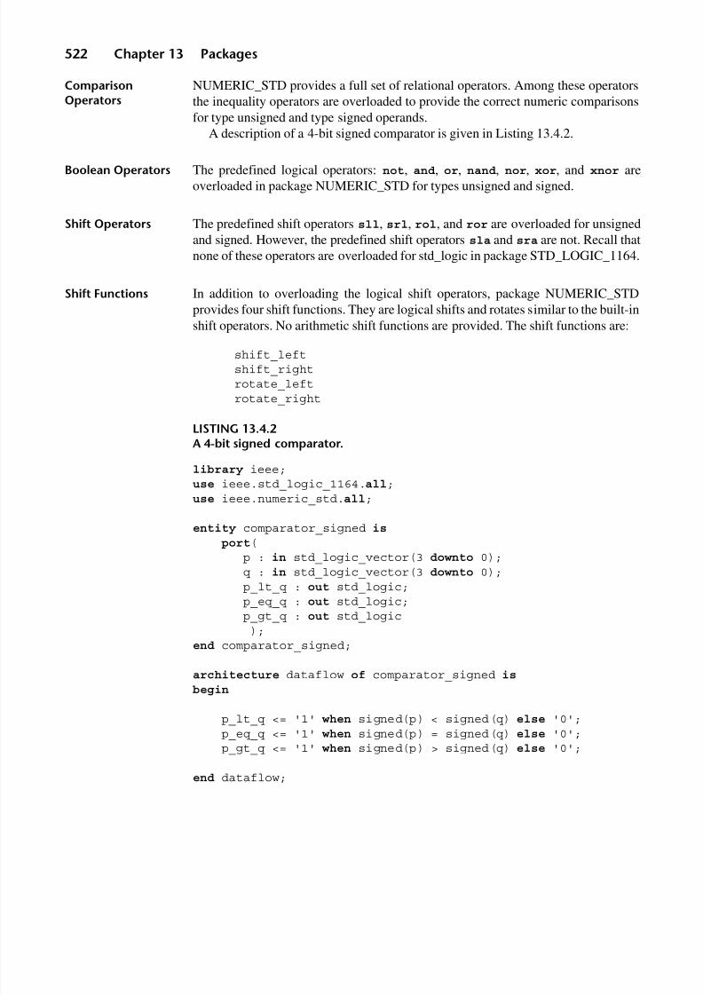
8/9/2019 VHDL for Engineers - Kenneth L. Short.pdf
http://slidepdf.com/reader/full/vhdl-for-engineers-kenneth-l-shortpdf 555/719
522 Chapter 13 Packages
ComparisonOperators
NUMERIC_STD provides a full set of relational operators. Among these operatorsthe inequality operators are overloaded to provide the correct numeric comparisonsfor type unsigned and type signed operands.
A description of a 4-bit signed comparator is given in Listing 13.4.2.
Boolean Operators The predefined logical operators: not, and, or, nand, nor, xor, and xnor areoverloaded in package NUMERIC_STD for types unsigned and signed.
Shift Operators The predefined shift operators sll, srl, rol, and ror are overloaded for unsignedand signed. However, the predefined shift operators sla and sra are not. Recall thatnone of these operators are overloaded for std_logic in package STD_LOGIC_1164.
Shift Functions In addition to overloading the logical shift operators, package NUMERIC_STDprovides four shift functions. They are logical shifts and rotates similar to the built-inshift operators. No arithmetic shift functions are provided. The shift functions are:
shift_leftshift_rightrotate_leftrotate_right
LISTING 13.4.2A 4-bit signed comparator.
library ieee;use ieee.std_logic_1164.all;
use ieee.numeric_std.all;
entity comparator_signed is
port(p : in std_logic_vector(3 downto 0);q : in std_logic_vector(3 downto 0);p_lt_q : out std_logic;p_eq_q : out std_logic;p_gt_q : out std_logic);
end comparator_signed;
architecture dataflow of comparator_signed is
begin
p_lt_q <= '1' when signed(p) < signed(q) else '0';p_eq_q <= '1' when signed(p) = signed(q) else '0';p_gt_q <= '1' when signed(p) > signed(q) else '0';
end dataflow;

8/9/2019 VHDL for Engineers - Kenneth L. Short.pdf
http://slidepdf.com/reader/full/vhdl-for-engineers-kenneth-l-shortpdf 556/719
Section 13.5 Package STD_LOGIC_ARITH 523
These functions all take two parameters. The first is the unsigned or signed valueto shift. The second is a type natural value that specifies the shift distance. Since thesecond parameter is type natural, each shift is in only one direction.
Type Conversions Functions are provided in package NUMERIC_STD to provide conversions between
types unsigned, signed, and integer. These functions were introduced in Chapter 3.(See “Types Unsigned and Signed” on page 107.) All of these functions have thename to_type, where type is the type being converted to. When converting typeunsigned or type signed to integer, the function has a single parameter, the vectorbeing converted. When converting an integer to unsigned or signed, the function hastwo parameters. The first is the integer being converted, and the second is a typenatural that specifies the number of bits in the result vector.
13 .5 PA CK AG E S TD _LO GIC _ AR ITH
Package STD_LOGIC_ARITH predated package NUMERIC_STD and has foundwidespread use. It contains arithmetic functions that accept signed and unsignedparameter types and return std_logic types. This package has essentially the samefunctionality as NUMERIC_STD. While typically included in tool vendors’ IEEElibraries, this package is not an IEEE standard.
Many of the operators and functions in package STD_LOGIC_ARITH are exten-sively overloaded. This can sometimes cause ambiguities that create compiler errors.
Since IEEE Std 1076.6 limits the array types used to represent unsigned andsigned numbers to NUMERIC_STD and NUMERIC_BIT, use of package
STD_LOGIC_ARITH is precluded if strict adherence to IEEE Std 1076.6 is to bemaintained. However, use of this package is encountered in legacy code, so somefamiliarity with it is useful.
Resize Function STD_LOGIC_ARITH contains functions conv_unsigned and conv_signed thatare used to resize (truncate or extend) values of the respective types. These functionsare similar to the resize function in NUMERIC_STD, except for whenconv_signed is used to truncate a signed value. In this case, bits are truncated fromthe left to create a result of the desired size. This includes truncating the sign bit. If the original value is small enough to be represented in the truncated result, there isno change in sign. However, if the original value is too large to fit in the truncated
result, the value’s sign changes. This corresponds to the conventional approach tosigned number truncation. But, it is in contrast to the approach used by the resizefunction in NUMERIC_STD, where the sign bit is kept and then the necessarynumber of bits following the sign bit is truncated to create a result of the desired size.
ArithmeticOperators
There are fewer arithmetic operators in package STD_LOGIC_ARITH than inpackage NUMERIC_STD. STD_LOGIC_ARITH provides only the operators sign –,

8/9/2019 VHDL for Engineers - Kenneth L. Short.pdf
http://slidepdf.com/reader/full/vhdl-for-engineers-kenneth-l-shortpdf 557/719
524 Chapter 13 Packages
sign +, abs, +, –, and *. The unary sign operator (–) and the abs operator apply only tosigned type.
There are a large number of permutations of the arithmetic operators provided byoverloading. These permutations allow types to be mixed without type conversions.For example, an unsigned and a signed can be added and a signed result returned, or
an unsigned and a signed can be added and a std_logic_vector result returned.
ComparisonOperators
The complete set of comparison operators is provided. Comparison operators forunsigned and signed are defined to give the correct interpretations for theirrespective numeric representations. In addition, the operands compared do not haveto be the same length.
Shift Functions Because package STD_LOGIC_ARITH predates the 1993 version of the VHDLstandard, the shift operators introduced in that version are not supported. Instead, twoshift functions, shl and shr, are provided. Whereas VHDL’s built-in shift operatorsuse an integer to specify the number of bit positions to be shifted, STD_LOGIC_
ARITH requires the shift distance to be specified by an unsigned type.
Boolean Operators There are no logical operators provided in package STD_LOGIC_ARITH. Logicaloperations can be accomplished by converting the unsigned or signed operands tostd_logic_vector and using the STD_LOGIC_1164 logical operators. The std_logic_vector result can be converted back to either unsigned or signed.
Type Conversions Four different types are used in package STD_LOGIC_ARITH: unsigned, signed,std_logic_vector, and integer. Type conversions between std_logic_vector and eitherunsigned or signed are implicit conversions provided by the built-in conversionsbetween similar array types. Conversion functions are provided to accomplish theother type conversions. The functions are named conv_type where type is thename of the type being converted to.
Conversion functions that convert to an integer have only one formal parameter,the vector to be converted. Conversion functions that convert to a vector have twoformal parameters. The first parameter is the vector to be converted and the second isthe number of bits in the result vector. When the vector converted from and thevector converted to are the same type, the conversion function is acting as the previ-ously discussed, resize function.
1 3. 6 P ACK AG ES F OR VH DL TE XT OU TP UT
Several nonstandard packages are available to provide text output. One such packageis Stefan Doll’s package txt_util. This package is available on the Web andprovides a means to output text and manipulate strings. The package includesfunctions to convert various types to strings, procedures to print messages to thescreen, and to read and write strings to text files.
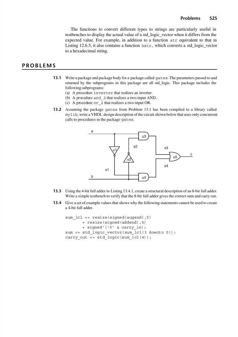
8/9/2019 VHDL for Engineers - Kenneth L. Short.pdf
http://slidepdf.com/reader/full/vhdl-for-engineers-kenneth-l-shortpdf 558/719
Problems 525
The functions to convert different types to strings are particularly useful intestbenches to display the actual value of a std_logic_vector when it differs from theexpected value. For example, in addition to a function str equivalent to that inListing 12.6.5, it also contains a function hstr, which converts a std_logic_vectorto a hexadecimal string.
PROBLE MS
13.1 Write a package and package body for a package called gates. The parameters passed to andreturned by the subprograms in this package are all std_logic. This package includes thefollowing subprograms:(a) A procedure inverter that realizes an inverter.(b) A procedure and_2 that realizes a two-input AND.(c) A procedure or_2 that realizes a two-input OR.
13.2 Assuming the package gates from Problem 13.1 has been compiled to a library called
mylib, write a VHDL design description of the circuit shown below that uses only concurrentcalls to procedures in the package gates.
13.3 Using the 4-bit full adder in Listing 13.4.1, create a structural description of an 8-bit full adder.Write a simple testbench to verify that the 8-bit full adder gives the correct sum and carry out.
13.4 Give a set of example values that shows why the following statements cannot be used to createa 4-bit full adder.
sum_lcl <= resize(signed(augend),5)+ resize(signed(addend),5)
+ signed'('0' & carry_in);sum <= std_logic_vector(sum_lcl(3 downto 0));carry_out <= std_logic(sum_lcl(4));
s1
a
b
c
s4
s3s2
u5
u3
u4
u2
u1

8/9/2019 VHDL for Engineers - Kenneth L. Short.pdf
http://slidepdf.com/reader/full/vhdl-for-engineers-kenneth-l-shortpdf 559/719
526
Chapter 14
Testbenches for Sequential Systems
Exhaustive verification is relatively easy to accomplish for combinational systems.In contrast, for even simple sequential systems it may be difficult. For complexsequential systems, it can be practically impossible. Accordingly, instead of anexhaustive verification, a comprehensive verification, one well short of exhaustive, isoften the objective. A comprehensive verification is one that provides a high degreeof confidence that a design is correct.
Achieving a comprehensive verification is predicated on how well the stimulus weapply covers the circumstances in which the UUT is expected to operate. Ultimately,our confidence in a verification is limited by the thoroughness and appropriateness of the stimulus.
Testbenches for sequential systems require generation of a clock and a resetsignal, in addition to data and control stimulus signals.
Use of procedures simplifies stimulus generation. Each procedure can be written tocreate the stimulus required to exercise a particular UUT operation or functionality. Withstimulus generation for each UUT operation encapsulated into a separate procedure, acomplex stimulus is created by simply calling these procedures in the desired order.
1 4. 1 S IM PL E S EQ UE NT IA L TE ST BE NC HE S
Figure 7.1.1, which shows the constituents of a simple combinational testbench, ismodified in Figure 14.1.1 to represent the constituents of a simple sequential testbenchby adding a system clock and a reset.
System Clockand System Reset
All synchronous systems require a system clock signal. Accordingly, their testbenchesmust provide this signal. Generation of an accurate system clock is important, because

8/9/2019 VHDL for Engineers - Kenneth L. Short.pdf
http://slidepdf.com/reader/full/vhdl-for-engineers-kenneth-l-shortpdf 560/719
Section 14.2 Generating a System Clock 527
other stimulus signals are ususally synchronized to the system clock. The system clock
must accurately model the clock that will exist in the UUT’s application environment.In addition to a system clock, a reset signal is required. The reset signal is asserted
at power on to place the sequential system in its initial state. The reset stimulus mustaccurately model the reset signal in the UUT’s application environment.
1 4. 2 G EN ER AT IN G A S YS TE M C LO CK
Since other stimulus signals in the testbench are usually synchronized to the systemclock, its generation is considered first. A system clock can easily be generated using
either a concurrent signal assignment statement or a process. Use of a processprovides greater flexibility.
50% Duty CycleClock
System clocks are often specified as having a 50% duty cycle. An example of a 50%duty cycle clock generated using a concurrent signal assignment statement is
clk <= not clk after period/2;
where constant period specifies the clock’s period and is declared in the declarativepart of the testbench architecture. Signal clk must be given an initial value of either
'0' or '1' when it is declared. Otherwise, since the not of 'U' is 'U', the clock would remain 'U' throughout the simulation.An example of a process that generates a 50% duty cycle clock is given in Listing
14.2.1.In Listing 14.2.1, constant period is declared in the declarative part of the
process. An assignment statement makes the initial phase of the clock '0'. Next, aninfinite loop repeatedly waits for half the clock period and then complements theclock’s value.
FIGURE 14.1.1
Typical constituents of a simple sequential testbench.
StimulusGenerator
SystemClock
UUTResponseMonitor
SystemReset

8/9/2019 VHDL for Engineers - Kenneth L. Short.pdf
http://slidepdf.com/reader/full/vhdl-for-engineers-kenneth-l-shortpdf 561/719
528 Chapter 14 Testbenches for Sequential Systems
LISTING 14.2.1Process to generate a 50% duty cycle clock.
clock_gen: process
constant period : time := 100 ns;begin
clk <= '0'; -- Initial phase of the clock loop
wait for period/2;clk <= not clk;
end loop;end process;
Stopping the Clockin a Simulation
As discussed in Chapter 6, a simulation stops when a specified simulation time limitis reached or when there are no more events to simulate. It is sometimes more conve-nient to run a simulation without having to specify a time limit. We must then depend
on the simulation stopping when there are no more events.When simulating a combinational system without using a time limit, after the laststimulus value has been applied and the events associated with it have beensimulated, there are no more events for the simulator to process and the simulationstops.
However, when simulating a sequential system without using a time limit, thesystem clock generated by either of the previous methods runs continuously. Thesimulation does not end because the clock is always generating new events, evenafter the last data or control stimulus has been applied. As a result, if the clock is notstopped, the simulation does not stop.
Using a BooleanSignal to Stop theClock
A boolean signal can be used to stop the clock. For example, if boolean signalend_sim is assigned the value false at the beginning of the testbench, the clock inListing 14.2.2 runs until end_sim is assigned the value true.
LISTING 14.2.2Clock that is stopped by an external signal.
clock_gen : process
begin
clk <= '0';loop
wait for period/2;clk <= not clk;exit when end_sim = true;
end loop; wait;
end process;

8/9/2019 VHDL for Engineers - Kenneth L. Short.pdf
http://slidepdf.com/reader/full/vhdl-for-engineers-kenneth-l-shortpdf 562/719
Section 14.2 Generating a System Clock 529
LISTING 14.2.3Process to create a clock with a specified duty cycle.
clock_gen: process
constant duty_cycle : real := 0.40;constant period : time := 100 ns ;
constant clk_high : time := duty_cycle * period ;begin
loop
clk <= '0'; wait for period - clk_high; -- clock low timeclk <= '1'; wait for clk_high; -- clock high time
end loop;end process;
end behavioral;
After the stimulus process has finished applying stimulus to the UUT, it assignsthe value true to end_sim. At that point, the clock process exits its loop andexecutes an infinite wait. There are then no more events for the simulator to processand the simulation ends.
To stop the system clock, a boolean signal, like end_sim, can be added to anyclock description.
NonsymmetricalClock
A clock’s specification may call for a duty cycle other than 50%. In such cases, weneed to be able to specify how long the clock is high (or low), in addition to speci-fying its period. The process in Listing 14.2.3 generates a clock with a specified duty
cycle.This example is for a clock having a 40% duty cycle. The clk_high time is
specified as a constant whose value is the product of the duty cycle and clock period.The clk_low time is simply the clock period minus the clk_high time. The resultingwaveform is shown in Figure 14.2.1.
ConcurrentProcedure Clock
Instead of a concurrent signal assignment or a process, a concurrent procedure canbe used to generate a clock. A clock described by a concurrent procedure can beplaced in a package for easy reuse in other testbenches.
FIGURE 14.2.1
Clock waveform from process in Listing 14.2.3 and reset waveform fromprocess in Listing 14.3.2.

8/9/2019 VHDL for Engineers - Kenneth L. Short.pdf
http://slidepdf.com/reader/full/vhdl-for-engineers-kenneth-l-shortpdf 563/719
530 Chapter 14 Testbenches for Sequential Systems
Phase-RelatedPeriodicWaveforms
In addition to the system clock, some data or control inputs to a sequential systemmay also be in the form of periodic signals. For example, if a system receives inputsfrom an optical shaft encoder, these inputs can be modeled as two periodic signalswith a 90-degree phase shift.
Listing 14.2.4 uses two calls to the concurrent procedure clock_gen, declared in
the declarative part of the architecture, to generate a two-phase clock correspondingto the outputs of an optical shaft encoder (OSE).
Procedure clock_gen has one formal parameter that is a signal of mode out andthree formal parameters that are constants of mode in. After waiting for a period of time equal to the desired phase shift, the procedure enters an infinite loop where itrepeatedly generates a signal that is a '1' for a time equal to high, and then is '0'for a time equal to period minus high. Note that there is no actual subtractionoperation in this code.
Inside the loop, the assignment to clk is a waveform that is '1' initially, and thenchanges to '0' after high ns. The wait statement following the assignment to clk
suspends the procedure and causes two transactions to be posted to the driver for clk.After period ns, the procedure becomes active again and the assignment to clk isexecuted again, causing the clock waveform to repeat with the specified period.
LISTING 14.2.4Two-phase clock generated by concurrent calls to a procedure.
library ieee;use ieee.std_logic_1164.all;
entity shaft_encoder is
port(
clk_a : out std_logic;clk_b : out std_logic);
end shaft_encoder;
architecture behavioral of shaft_encoder is
procedure clock_gen (signal clk: out std_logic;constant period, high, phase : in time ) is
begin
clk <= '0'; wait for phase;loop
clk <= '1', '0' after high; wait for period;
end loop;end clock_gen;
begin
clock_gen (clk_a, 100 ns, 50 ns, 0 ns);clock_gen (clk_b, 100 ns, 50 ns, 25 ns);
end behavioral;

8/9/2019 VHDL for Engineers - Kenneth L. Short.pdf
http://slidepdf.com/reader/full/vhdl-for-engineers-kenneth-l-shortpdf 564/719
Section 14.3 Generating the System Reset 531
In the statement part of the architecture, there are two concurrent procedure callsto generate the two-phase clock representing the OSE’s output. The two proceduresare invoked during the initialization phase of the simulation. Neither procedure isever returned from. The resulting waveforms appear in Figure 14.2.2.
1 4. 3 G EN ER AT IN G T HE SYS TE M R ES ET
The reset signal to a hardware system typically starts in its asserted state at power on,remains in that state for a specified period of time, then changes to its unassertedstate and remains there for as long as power continues to be applied to the system.The duration of the assertion of the reset signal is specified as either a fixed time orsome multiple of the clock’s period, and should be synchronized to the system clock to properly reset the UUT.
Generating a fixed-duration reset pulse is simple. For example, if the reset signalshould be '0' for 160 ns and then become '1', a concurrent signal assignment canbe used:
reset_bar <= '0', '1' after 160 ns;
Alternatively, but less concisely, a reset process can be written as in Listing 14.3.1.
SynchronizingReset Duration tothe System Clock
If the reset pulse duration is specified as some minimum number of clock periods,then the reset can be written to synchronize its duration to the clock, as shown inListing 14.3.2.
LISTING 14.3.1Process for a fixed-duration reset pulse.
reset: process
begin
reset_bar <= '0'; wait for 160 ns;reset_bar <= '1'; wait;
end process;
FIGURE 14.2.2Two-phase waveform generated by concurrent procedure calls in Listing 14.2.4.

8/9/2019 VHDL for Engineers - Kenneth L. Short.pdf
http://slidepdf.com/reader/full/vhdl-for-engineers-kenneth-l-shortpdf 565/719
532 Chapter 14 Testbenches for Sequential Systems
LISTING 14.3.2Process for a reset pulse whose duration is a multiple of the clock period.
reset: process
begin
reset_bar <= '0';
for i in 1 to 2 loop wait until clk = '1';end loop;reset_bar <= '1'; wait;
end process;
This process first assigns a '0' to reset_bar. A loop then counts two risingedges of clk. After these two rising edges, reset_bar is assigned a '1'.
An advantage of this approach is that if the system clock period is changed, the
reset pulse is automatically adjusted to provide the minimum required duration.
1 4. 4 S YN CH RO NI ZI NG S TI MU LU S G EN ER AT IO N A N D M O N I T O R I N G
In this section we consider some issues associated with synchronizing stimulusgeneration and output verification to the system clock.
Stimulus Timing A system’s specification may include an interface timing specification that detailsinput signal timing. If so, the testbench’s stimulus must accurately model the timingspecified. We consider generating stimulus that meets detailed interface timingspecifications in Section 14.9. In this section, our attention is on generating stimuluswhen the exact interface timing is not specified. This is appropriate when a system isbeing designed for generic applications.
Testbench for aTwo-Bit Counter
An example of a testbench for a 2-bit counter illustrates some timing issues of concern.Assume that the UUT in Figure 14.1.1 is a 2-bit binary counter with only clock and
reset inputs. Also assume that the system clock is generated by the process in Listing14.2.2 and the reset signal is generated by the process in Listing 14.3.2.
SynchronizingReset to the SystemClock
The reset signal is synchronized to the system clock. Initially, rst_bar is asserted.A loop is then used to wait until the first two triggering clock edges have occurred.When the loop is completed, rst_bar is unasserted. The waveforms produced bythis simulation appear on a waveform viewer, as shown in Figure 14.4.1.

8/9/2019 VHDL for Engineers - Kenneth L. Short.pdf
http://slidepdf.com/reader/full/vhdl-for-engineers-kenneth-l-shortpdf 566/719
Section 14.4 Synchronizing Stimulus Generation and Monitoring 533
Effect of DeltaDelays
Looking at the clk and rst_bar signals, it might appear from Figure 14.4.1 that, fora functional simulation, the counter will starting counting at the second triggeringclock edge. However, by examining the code in Listing 14.3.2, we see that the resetprocess suspends each time the statement
wait until clk = '1':
is executed. During the same simulation cycle where clk changes from 0 to 1 for thesecond time, the reset process resumes execution and the statement
rst_bar <= '1';
is executed, followed by the instruction:
wait;
When the wait instruction is executed, the reset process suspends and the trans-action that changes rst_bar to a '1' is posted with a time component 1
δlater than
the current simulation time. Thus, it is not until the next simulation cycle (a deltacycle) that rst_bar is actually changed to a '1'. Since the waveform viewer doesnot show delta cycles, the 1 δ delay is not visible in Figure 14.4.1. The actualrelationship between the clock and reset signals is represented in Figure 14.4.2. As aresult, the counter does not start counting until the third triggering clock edge. Thus,in a functional simulation, a δ delay can have the same effect as delaying an entireclock cycle. Knowing when the counter actually starts to count is critical forcorrectly writing the monitor.
FIGURE 14.4.1
Waveforms for functional simulation of 2-bit counter.
FIGURE 14.4.2
Actual delta delay between the clock triggering edge and synchronized reset.
clk
rst_bar

8/9/2019 VHDL for Engineers - Kenneth L. Short.pdf
http://slidepdf.com/reader/full/vhdl-for-engineers-kenneth-l-shortpdf 567/719
534 Chapter 14 Testbenches for Sequential Systems
Synchronizingthe Monitor
Output verification must be synchronized to the system clock. Assume that we wantto write a process to verify the 2-bit counter’s outputs. The monitor process mustwait until after the first two triggering clock edges. Then, after each subsequenttriggering clock edge, the monitor process can use an assertion statement to verifythe counter’s output value. For example, if, after the first two triggering clock edges,
we wanted to wait for the third triggering clock edge and then check for a count of "01", we might attempt to use the following sequence of statements:
wait until clk = '1';assert count = "01"report "missed count 01"severity error;
The monitor process containing these statements is resumed during the simulationcycle where the event corresponding to the triggering clock edge occurs. During thissame simulation cycle, the counter process is also resumed. The counter process posts atransaction assigning count the value "01". This value will not take effect until thenext simulation cycle. However, during the current simulation cycle, the assertionstatement verifies whether count is "01". Since it is not (yet), an error is erroneouslyreported.
To achieve proper verification, the assertion statement must wait until after countactually takes its new value. This can be done by waiting for any small nonzero timeafter the triggering clock edge. For example, the code
wait until clk = '1'; wait for 1 ns;assert count = "01"
report "missed count 01"severity error;
works correctly, since the additional wait for 1 ns ensures that the counter has takenits new value in response to the triggering clock edge.
The monitor process in Listing 14.4.1 can be used to exhaustively verify theoutputs of a n-bit binary counter.
LISTING 14.4.1Monitor process for n-bit binary counter.
monitor: process
constant n : integer := 2; -- number of bits in counter begin
for i in 1 to 2 loop -- skip clocks while counter is reset wait until clk = '1';
end loop; wait for 1 ns;
-- verify counter’s output after each clock

8/9/2019 VHDL for Engineers - Kenneth L. Short.pdf
http://slidepdf.com/reader/full/vhdl-for-engineers-kenneth-l-shortpdf 568/719
Section 14.4 Synchronizing Stimulus Generation and Monitoring 535
for i in 0 to 2**n loop -- count until clock rolls over to 0assert count = (std_logic_vector(to_unsigned(i mod 2**n, n)))report "Count of " & integer'image(i mod 2**n) & " failed"severity error; wait until clk = '1'; wait for 1 ns;
end loop;
end_sim <= true; wait;
end process;
The first loop in process monitor skips the first two triggering clock edges,which occur while the counter is reset. Since we are skipping the clock edges thatoccur while the counter is reset, a simpler alternative is to replace the first loop withthe instruction:
wait until rst_bar = '1';
The second loop verifies the counter’s output prior to the first triggering clock edgethat is counted, and then 1 ns after each of the next 2n triggering clock edges. Thus, thecounter’s output is checked as it counts from 0 to 2n – 1 and then rolls over to 0. Thismonitor process provides an exhaustive verification for this simple counter.
If the instruction
wait for 1 ns;
is removed from the second loop, count will be erroneously reported as incorrectfor all but the initial count after reset.
Note that, in this example, to stop the simulation the monitor process assignsend_sim the value true after the end of the second loop.
SynchronizingMonitoring for aTiming Simulation
While waiting for any small nonzero delay after the triggering clock edge worksfor a functional simulation, a timing simulation is more complicated. If thesystem’s specification specifies a maximmum delay, then that is the value thatmust be used. If not, the delay must be greater the propagation delay of the UUTtiming model.
A simple approach that usually allows the same testbench to be used for bothfunctional and timing simulations, when a timing specification is not given, is to
synchronize monitoring to the nontriggering clock edge. For a system with a 50%duty cycle clock, this gives half a clock period for output signal transitions due topropagation delay in the UUT to settle.
SynchronizingStimulus to SystemClock
Our simple counter example has no inputs other than its clock and reset. A morecomplex counter would have additional inputs such as count enable, countdirection, load enable, and load data. As synchronous inputs, they would also need

8/9/2019 VHDL for Engineers - Kenneth L. Short.pdf
http://slidepdf.com/reader/full/vhdl-for-engineers-kenneth-l-shortpdf 569/719
536 Chapter 14 Testbenches for Sequential Systems
to be synchronized to the system clock. Usually, their values would be expected tobecome valid just after the preceding triggering clock edge. When exact timing is notspecified, also synchronizing these stimuli to the nontriggering clock edge is oftenappropriate.
Testbench forDigital Noise Filter
A testbench for the digital noise filter from Figure 9.2.3 and Listing 9.2.4 illustratessynchronizing stimulus and monitoring to the falling edge of the system clock.
LISTING 14.4.2Testbench for digital noise filter from Figure 9.2.3 and Listing 9.2.4.
library ieee;use ieee.std_logic_1164.all;
entity filter_tb is
end filter_tb;
architecture tb_architecture of filter_tb is
-- Stimulus signals - signals mapped to the input and inout ports of UUT signal cx : std_logic;signal clk : std_logic := '0';signal rst_bar : std_logic;-- Observed signals - signals mapped to the output ports of UUT signal y : std_logic;signal end_sim : boolean := false;
constant period : time := 100 ns;
-- stimulus and response signal valuesconstant inputs : std_logic_vector := "0011011100110001011";constant outputs : std_logic_vector := "0000000001111111000";
begin
-- Unit Under Test port mapUUT : entity filterport map (cx => cx, clk => clk, rst_bar => rst_bar, y => y );
-- system clock generation
cpu_clock_gen : clk <= not clk after period/2 when end_sim = false else unaffected;
-- system reset generationreset_gen : rst_bar <= '0', '1' after 2 * period;
-- stimulus and response processstim_respon : process

8/9/2019 VHDL for Engineers - Kenneth L. Short.pdf
http://slidepdf.com/reader/full/vhdl-for-engineers-kenneth-l-shortpdf 570/719
Section 14.4 Synchronizing Stimulus Generation and Monitoring 537
begin
wait until rst_bar = '1';for i in inputs'range loop
cx <= inputs(i); wait until clk = '0';assert y = outputs(i)report "system failure at " & integer'image(i) & " clocks after reset"severity error;
end loop;end_sim <= true; wait;
end process;end tb_architecture;
In Listing 14.4.2 the single process stim_respon is used to both generate thestimulus and verify the response. The first time this process is executed, it suspends
and waits for rst_bar to be unasserted. After rst_bar is unasserted, it resumes andenters the loop. The first time through the loop, the process applies the first inputvalue from a sequence of input values represented by the vector inputs and thensuspends waiting for the falling edge of the clock.
Subsequently, on the falling edge of each clock pulse, the process verifies theoutput by comparing its value to the corresponding element in the vector outputsof expected output values. It then applies the next input value and suspends waitingfor the next falling edge of the clock. After all of the input values have been appliedand their outputs verified, the loop terminates. Signal end_sim is assigned the valuetrue and the simulation ends. The waveforms from this simulation are given inFigure 14.4.3.
The verification provided by this testbench is clearly not exhaustive. It can bemade more comprehensive by adding additional carefully selected values to thevectors inputs and outputs.
FIGURE 14.4.3
Waveforms for simulation of digital noise filter using testbench inListing 14.4.2.

8/9/2019 VHDL for Engineers - Kenneth L. Short.pdf
http://slidepdf.com/reader/full/vhdl-for-engineers-kenneth-l-shortpdf 571/719
538 Chapter 14 Testbenches for Sequential Systems
1 4. 5 TE ST BE NC H F OR SU CC ES SI VE A P P R O X I M A T I O N R E G I S T E R
A testbench for the successive approximation register (SAR) design from Section
11.4 illustrates the complete design of a sequential testbench and its use of a systemclock and a system reset. It also demonstrates the use of a procedure to synchronizeactions in the stimulus and response process to the operation of the UUT. Thetestbench structure is shown in Figure 14.5.1.
The testbench’s architecture contains five concurrent statements:
• Instantiation of SAR as the UUT
• Process to generate system clock
• Concurrent signal assignment to generate system reset
• Concurrent signal assignment to model DAC and comparator
•Process to provide stimulus and to monitor response
The stimulus-and-response process generates a value corresponding to the analoginput voltage to be converted, and generates the start of conversion signal soc to theSAR. At the completion of a conversion, this same process compares the conversionresult to the analog input value that was converted. The testbench code is given inListing 14.5.1.
DAC and AnalogComparator Model
The DAC has digital inputs and an analog output. The analog comparator has analoginputs and a digital output. At first thought, it might seem that, due to the analog nature
FIGURE 14.5.1
Structure of successive approximation register testbench.
comp_in comp_out
DAC and ComparatorModelSAR
result
8
soc
eoc
Stimulus andMonitor
analog_unknown(digital representation
of analog input voltage)
8

8/9/2019 VHDL for Engineers - Kenneth L. Short.pdf
http://slidepdf.com/reader/full/vhdl-for-engineers-kenneth-l-shortpdf 572/719
Section 14.5 Testbench for Successive Approximation Register 539
LISTING 14.5.1Successive approximation register (SAR) testbench.
library ieee;use ieee.std_logic_1164.all;use ieee.numeric_std.all;
entity saadc_tb is
end saadc_tb;
architecture tb_architecture of saadc_tb is
-- stimulus signalssignal reset_bar : std_logic;signal soc : std_logic;signal comp_in : std_logic;signal clk : std_logic := '0';
-- observed signalssignal eoc : std_logic;signal result : std_logic_vector(7 downto 0);signal analog_unknown : std_logic_vector(7 downto 0);
constant period : time := 100 ns;signal end_sim : boolean := false;
begin
-- unit under test instantiationuut : entity saadcport map (reset_bar => reset_bar, soc => soc, comp_in => comp_in,
clk => clk, eoc => eoc, result => result );
-- system clock generationcpu_clock_gen : process
begin
clk <= '0'; wait for period/2;loop
clk <= not clk; wait for period/2;exit when end_sim = true;
end loop; wait;
end process;
-- system reset generationreset_gen : reset_bar <= '0', '1' after 2 * period;
(Cont.)

8/9/2019 VHDL for Engineers - Kenneth L. Short.pdf
http://slidepdf.com/reader/full/vhdl-for-engineers-kenneth-l-shortpdf 573/719
540 Chapter 14 Testbenches for Sequential Systems
LISTING 14.5.1 (Cont.)
-- DAC and analog comparator model instantiationcomp_in <= '1' after 10 ns when analog_unknown >= result else '0' after 10 ns;
-- stimulus and responsestim_resp: Process
-- definition of procedure to control soc for a conversionprocedure soc2eoc is
begin
wait until falling_edge(clk);soc <= '1'; wait until eoc = '1';soc <= '0'; wait until rising_edge(clk);
end procedure ;
begin-- intialize soc and wait until reset is completesoc <= '0'; wait until reset_bar = '1'; wait until rising_edge(clk);
-- apply every possible analog unknown valuefor i in 0 to 255 loop
analog_unknown <= std_logic_vector(to_unsigned(i,8));soc2eoc; -- start conversion and wait for its end assert result = analog_unknownreport "conversion failed for analog unknown equal to " &integer'image(i)severity error;
end loop;end_sim <= true;
wait;end process;
end tb_architecture;
of these devices, they would be difficult to model in VHDL. However, modeling theDAC and comparator together as a single entity is surprisingly simple.
In the successive approximation ADC, the analog output of the DAC provides oneof the inputs to the analog comparator (Figure 11.4.1). When combined, the DACand analog comparator have only one analog input signal, the analog voltage to beconverted. If this signal is represented in the simulation as a digital value (analog_unknown), the DAC and analog comparator combination is then simply equivalentto a digital comparator (Figure 14.5.1). One input to this digital comparator is theresult from the SAR’s output and the other is the digital representation of the analog

8/9/2019 VHDL for Engineers - Kenneth L. Short.pdf
http://slidepdf.com/reader/full/vhdl-for-engineers-kenneth-l-shortpdf 574/719
Section 14.5 Testbench for Successive Approximation Register 541
input voltage to be converted. The digital comparator’s output corresponds to theanalog comparator’s output. As a result, the DAC and analog comparator combi-nation is modeled by the concurrent signal assignment statement:
comp_in <= '1' after 10 ns
when analog_unknown >= resultelse '0' after 10 ns;
The 10 ns delays specified by the after clauses model the combined delay of theDAC and analog comparator. Typically, this value is much greater than 10 ns for anactual DAC and analog comparator. For a timing simulation, the actual DAC andanalog comparator combined delay must be used.
SAR TestbenchStimulus-and-Response Process
The stimulus-and-response process (stim_resp) uses procedure soc2eoc, declaredin the declarative part of the process, to assert soc to start a conversion. This procedurethen waits until the conversion is complete (eoc = '1') to unassert soc. Use of this
procedure simplifies the body of the process.
Exhaustive SARVerification
In the statement part of the stim_resp process, soc is unasserted and then theprocess waits for the completion of the system reset. A loop then successivelygenerates the digital representation of all possible values for the analog inputvoltage. Since this is an 8-bit converter, the digital values corresponding to the rangeof the analog input voltage are from 0 to 255.
Each time through the loop, the next value in its range is assigned to analog_
unknown. The soc2eoc procedure is then called to initiate a conversion and to waituntil the conversion ends. After this procedure returns, an assert statement compares
the conversion result with analog_unknown and reports an error if they are notequal. When the loop is completed, the end_sim signal is assigned the value true,and the simulation terminates.
This simulation is exhaustive, since the functionality of the system is verified forevery possible analog input value. An exhaustive verification is feasible for thissequential system because, while its internal operation is sequential, the result froma conversion is a function of only the current analog input value to be converted.Figure 14.5.2 shows the waveforms for the first four loop iterations.
ComprehensiveSAR Verification
As discussed in Chapter 11, the number of bits in the SAR is easily increased tocreate a larger ADC. The same testbench is easily modified to handle a SAR with alarger number of bits. For a larger number of bits, the time required to simulate eachconversion as well as the number of conversions that must be simulated forexhaustive verification increases exponentially. This raises the question of whetheran exhaustive functional verification is required or whether a nonexhaustive and lesstime-consuming comprehensive verification might be adequate.
For example, we might decide that a simulation that includes conversion of valuesfor analog_unknown corresponding to the endpoints of the ADC input range (0 and
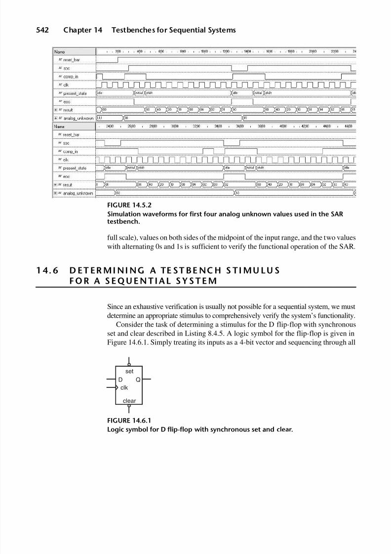
8/9/2019 VHDL for Engineers - Kenneth L. Short.pdf
http://slidepdf.com/reader/full/vhdl-for-engineers-kenneth-l-shortpdf 575/719
542 Chapter 14 Testbenches for Sequential Systems
full scale), values on both sides of the midpoint of the input range, and the two valueswith alternating 0s and 1s is sufficient to verify the functional operation of the SAR.
1 4. 6 D ET ER MI NI NG A TE ST BE NC H S TI MU LU S
F O R A S E Q U E N T I A L S Y S T E M
Since an exhaustive verification is usually not possible for a sequential system, we mustdetermine an appropriate stimulus to comprehensively verify the system’s functionality.
Consider the task of determining a stimulus for the D flip-flop with synchronousset and clear described in Listing 8.4.5. A logic symbol for the flip-flop is given inFigure 14.6.1. Simply treating its inputs as a 4-bit vector and sequencing through all
FIGURE 14.5.2
Simulation waveforms for first four analog unknown values used in the SARtestbench.
FIGURE 14.6.1
Logic symbol for D flip-flop with synchronous set and clear.
clk
clear
setD Q

8/9/2019 VHDL for Engineers - Kenneth L. Short.pdf
http://slidepdf.com/reader/full/vhdl-for-engineers-kenneth-l-shortpdf 576/719
Section 14.6 Determining a Testbench Stimulus for a Sequential System 543
16 combinations in binary is not meaningful with respect to the flip-flop’s function-ality, and it represents only one of many possible input sequences.
Functionality BasedStimulus Sequence
To provide a comprehensive verification, we need to determine a stimulus that appro-priately exercises the system’s functionality.
Column one in Table 14.6.1 lists an appropriate sequence of D flip-flop opera-tions to use as a basis for a comprehensive verification. Each operation is chosen tochange the state of the flip-flop using the most appropriate values on all of its inputs.For example, when we verify the clear operation, we make the D input a 1, so that wecan be sure the effect of the operation was a clear, and not a load of 0 from input D.
First in the sequence of operations is the clear operation. If this operation issuccessful, the flip-flop’s output is 0. The next operation is to load a value into theflip-flop using its D input. The value we need to load is a 1. If we load a 0, we willnot be able to tell if the load operation was successful or if it had no effect and we aresimply observing the 0 previously stored as a result of the clear operation.
The last column of the table lists the expected output value after each operation.
The expected value for q is the value after a triggering clock edge, assuming thecorresponding inputs are stable before the triggering clock edge.
The desired stimulus-and-response waveforms are given in Figure 14.6.2.
Setup Timeand Hold TimeConsiderations
An important consideration is when stimulus values should be changed relative to theclock. If we consider only what is required for a functional simulation, inputs can bechanged any time prior to the clock, even as late as simultaneously with the clock edge.Inputs can be changed to the next combination as early as one delta after the clock edge.
It is advantageous to create a stimulus that is appropriate for both the functionalsimulation and the timing simulation, so the same testbench can be used.
When a system is being designed for use in a specific application environment,the timing of stimulus signals should model that environment. For example, if system inputs will be from a microprocessor’s system bus, then the bus timing speci-fication determines when stimulus values change.
For proper operation of a PLD, synchronous input values must be stable prior tothe triggering clock edge for a time equal to or exceeding the PLD’s setup time and
Table 14.6.1A sequence of operations as stimulus to a D flip-flop.
Operation d set_bar clr_bar Expected q
clear 1 1 0 0load 1 1 1 1 1
load 0 0 1 1 0
set 0 0 1 1
load 0 0 1 1 0
load 1 1 1 1 1
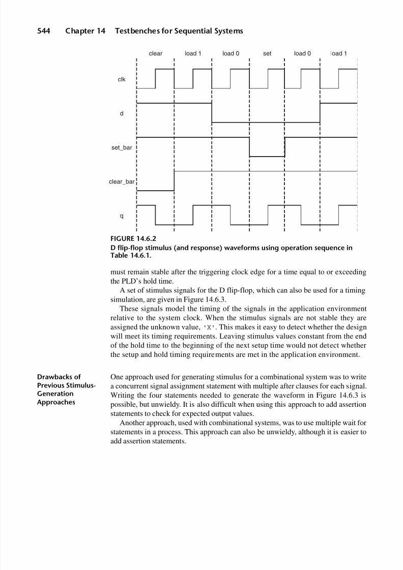
8/9/2019 VHDL for Engineers - Kenneth L. Short.pdf
http://slidepdf.com/reader/full/vhdl-for-engineers-kenneth-l-shortpdf 577/719
544 Chapter 14 Testbenches for Sequential Systems
must remain stable after the triggering clock edge for a time equal to or exceedingthe PLD’s hold time.
A set of stimulus signals for the D flip-flop, which can also be used for a timingsimulation, are given in Figure 14.6.3.
These signals model the timing of the signals in the application environmentrelative to the system clock. When the stimulus signals are not stable they areassigned the unknown value, 'X'. This makes it easy to detect whether the designwill meet its timing requirements. Leaving stimulus values constant from the endof the hold time to the beginning of the next setup time would not detect whetherthe setup and hold timing requirements are met in the application environment.
Drawbacks of
Previous Stimulus-GenerationApproaches
One approach used for generating stimulus for a combinational system was to write
a concurrent signal assignment statement with multiple after clauses for each signal.Writing the four statements needed to generate the waveform in Figure 14.6.3 ispossible, but unwieldy. It is also difficult when using this approach to add assertionstatements to check for expected output values.
Another approach, used with combinational systems, was to use multiple wait forstatements in a process. This approach can also be unwieldy, although it is easier toadd assertion statements.
FIGURE 14.6.2
D flip-flop stimulus (and response) waveforms using operation sequence inTable 14.6.1.
clear
clk
d
set_bar
clear_bar
q
load 1 load 0 set load 0 load 1

8/9/2019 VHDL for Engineers - Kenneth L. Short.pdf
http://slidepdf.com/reader/full/vhdl-for-engineers-kenneth-l-shortpdf 578/719
Section 14.7 Using Procedures for Stimulus Generation 545
Finally, using test vectors read from a table or a file is also unwieldy. These vectorsare difficult to write correctly and hard to interpret when applied to sequential systems.
In contrast to the previous approaches, use of multiple processes and procedures are
an effective way to generate stimulus. Examples of these approaches are presented inthe sections that follow.
1 4. 7 U SI NG PR OC ED UR ES FOR ST IM UL US G E N E R A T I O N
A useful approach to generating stimulus waveforms is to focus on the operationsthat can be performed by a UUT and write procedures to encapsulate the stimulus toactivate those operations. These procedures are written so that they synchronize
themselves to the system clock. In the testbench, these procedures are simply calledin the appropriate order to produce the desired sequence of UUT operations. Usingthis approach, the testbench stimulus is easier to code and maintain.
For example, operations for a D flip-flop require only three procedures: a setprocedure, a clear procedure, and a load procedure. The load procedure uses a parameterto specify whether a '0' or '1' is applied to the D input. The load procedure is shownin Listing 14.7.1.
FIGURE 14.6.3
D flip-flop stimulus (and response) waveforms for timing or functional simulation.
clear
clk
d
set_bar
clear_bar
q
load 1 load 0 set load 0 load 1
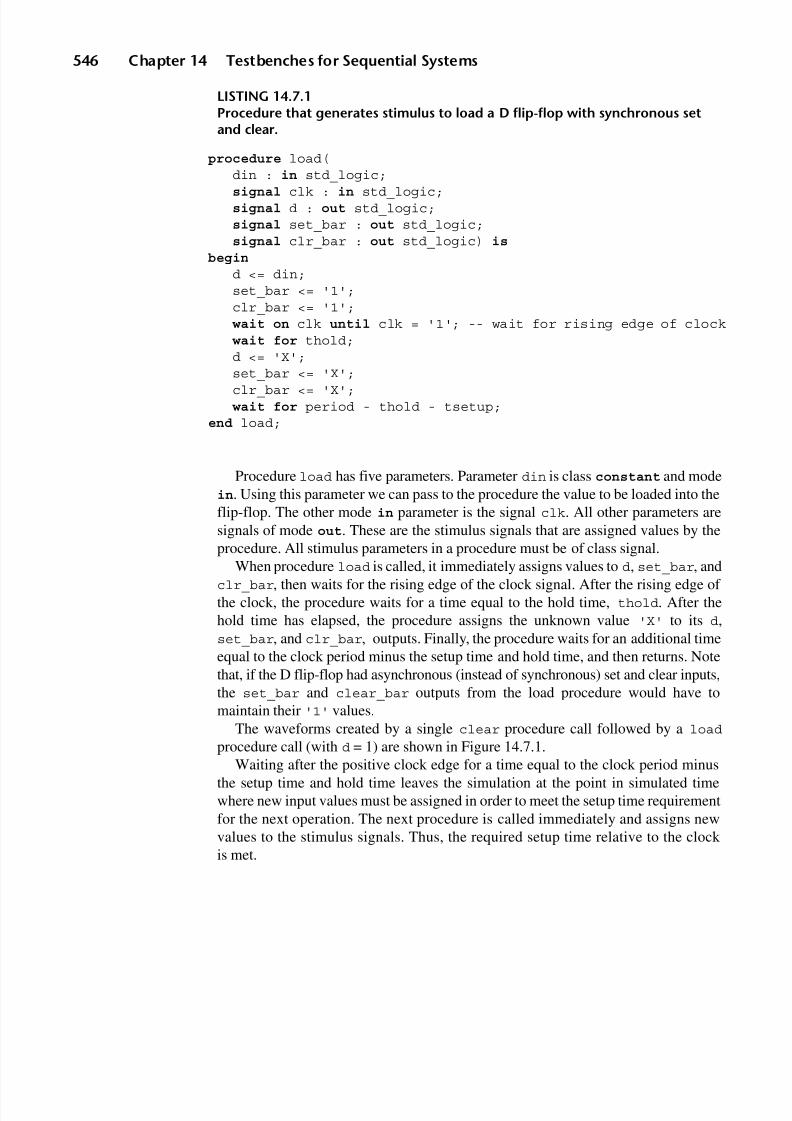
8/9/2019 VHDL for Engineers - Kenneth L. Short.pdf
http://slidepdf.com/reader/full/vhdl-for-engineers-kenneth-l-shortpdf 579/719
546 Chapter 14 Testbenches for Sequential Systems
LISTING 14.7.1Procedure that generates stimulus to load a D flip-flop with synchronous setand clear.
procedure load(din : in std_logic;
signal clk : in std_logic;signal d : out std_logic;signal set_bar : out std_logic;signal clr_bar : out std_logic) is
begin
d <= din;set_bar <= '1';clr_bar <= '1'; wait on clk until clk = '1'; -- wait for rising edge of clock wait for thold;d <= 'X';
set_bar <= 'X';clr_bar <= 'X'; wait for period - thold - tsetup;
end load;
Procedure load has five parameters. Parameter din is class constant and modein. Using this parameter we can pass to the procedure the value to be loaded into theflip-flop. The other mode in parameter is the signal clk. All other parameters aresignals of mode out. These are the stimulus signals that are assigned values by theprocedure. All stimulus parameters in a procedure must be of class signal.
When procedure load is called, it immediately assigns values to d, set_bar, andclr_bar, then waits for the rising edge of the clock signal. After the rising edge of the clock, the procedure waits for a time equal to the hold time, thold. After thehold time has elapsed, the procedure assigns the unknown value 'X' to its d,set_bar, and clr_bar, outputs. Finally, the procedure waits for an additional timeequal to the clock period minus the setup time and hold time, and then returns. Notethat, if the D flip-flop had asynchronous (instead of synchronous) set and clear inputs,the set_bar and clear_bar outputs from the load procedure would have tomaintain their '1' values.
The waveforms created by a single clear procedure call followed by a load
procedure call (with d = 1) are shown in Figure 14.7.1.Waiting after the positive clock edge for a time equal to the clock period minus
the setup time and hold time leaves the simulation at the point in simulated timewhere new input values must be assigned in order to meet the setup time requirementfor the next operation. The next procedure is called immediately and assigns newvalues to the stimulus signals. Thus, the required setup time relative to the clock is met.
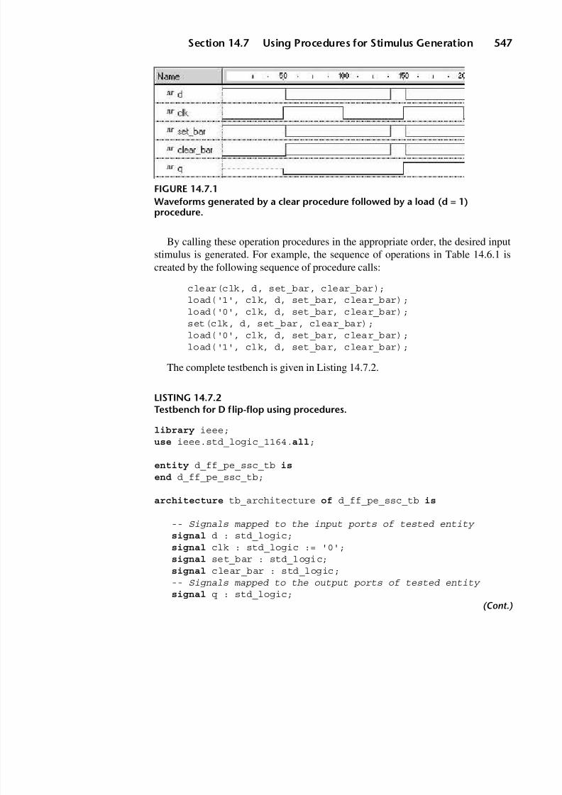
8/9/2019 VHDL for Engineers - Kenneth L. Short.pdf
http://slidepdf.com/reader/full/vhdl-for-engineers-kenneth-l-shortpdf 580/719
Section 14.7 Using Procedures for Stimulus Generation 547
By calling these operation procedures in the appropriate order, the desired inputstimulus is generated. For example, the sequence of operations in Table 14.6.1 is
created by the following sequence of procedure calls:
clear(clk, d, set_bar, clear_bar);load('1', clk, d, set_bar, clear_bar);load('0', clk, d, set_bar, clear_bar);set(clk, d, set_bar, clear_bar);load('0', clk, d, set_bar, clear_bar);load('1', clk, d, set_bar, clear_bar);
The complete testbench is given in Listing 14.7.2.
LISTING 14.7.2Testbench for D flip-flop using procedures.
library ieee;use ieee.std_logic_1164.all;
entity d_ff_pe_ssc_tb is
end d_ff_pe_ssc_tb;
architecture tb_architecture of d_ff_pe_ssc_tb is
-- Signals mapped to the input ports of tested entity
signal d : std_logic;signal clk : std_logic := '0';signal set_bar : std_logic;signal clear_bar : std_logic;-- Signals mapped to the output ports of tested entity signal q : std_logic;
(Cont.)
FIGURE 14.7.1
Waveforms generated by a clear procedure followed by a load (d = 1)procedure.

8/9/2019 VHDL for Engineers - Kenneth L. Short.pdf
http://slidepdf.com/reader/full/vhdl-for-engineers-kenneth-l-shortpdf 581/719
548 Chapter 14 Testbenches for Sequential Systems
LISTING 14.7.2 (Cont.)
-- Constantsconstant period : time := 100 ns;constant tsetup : time := 10 ns;constant thold : time := 2 ns;
-- Proceures to encapsulate operations
procedure clear(signal clk : in std_logic;signal d : out std_logic;signal set_bar : out std_logic;signal clr_bar : out std_logic) is
begin
d <= '1';set_bar <= '1';
clr_bar <= '0'; wait on clk until clk = '1'; wait for thold;d <= 'X';set_bar <= 'X';clr_bar <= 'X'; wait for period - thold - tsetup;
end clear;
procedure set(signal clk : in std_logic;signal d : out std_logic;signal set_bar : out std_logic;signal clr_bar : out std_logic) is
begin
d <= '0';set_bar <= '0';clr_bar <= '1'; wait on clk until clk = '1'; wait for thold;d <= 'X';set_bar <= 'X';clr_bar <= 'X';
wait for period - thold - tsetup;end set;
procedure load(din : in std_logic;signal clk : in std_logic;

8/9/2019 VHDL for Engineers - Kenneth L. Short.pdf
http://slidepdf.com/reader/full/vhdl-for-engineers-kenneth-l-shortpdf 582/719

8/9/2019 VHDL for Engineers - Kenneth L. Short.pdf
http://slidepdf.com/reader/full/vhdl-for-engineers-kenneth-l-shortpdf 583/719
550 Chapter 14 Testbenches for Sequential Systems
In the statement part of the architecture are:
• An instantiation statement to instantiate the flip-flop
• A concurrent signal assignment statement to generate the clock
• A process statement with a sequence of calls to the procedures
The waveforms generated are shown in Figure 14.7.2. Stimulus values are unknownuntil a time equal to the setup time before the clock’s rising edge. The stimulusvalues become unknown again, after a time equal to the hold time from the clock’srising edge. The clock’s period, setup time, and hold time are specified by constants inthe testbench.
1 4. 8 O UT PU T VE RI FI CA TI ON I N S TI MU LU S P R O C E D U R E S
This section discusses using assertion statements within stimulus procedures to verifyoutputs.
In Listing 14.8.1 the load procedure in Listing 14.7.1 is modified to includeassertion statements to verify the output.
LISTING 14.8.1Using assertion statements in a stimulus procedure to verify outputs.
procedure load(
din : in std_logic;signal clk : in std_logic;signal d : out std_logic;signal set_bar : out std_logic;signal clr_bar : out std_logic) is
begin
d <= din;set_bar <= '1';
FIGURE 14.7.2
Stimulus-and-response waveforms for D flip-flop testbench.

8/9/2019 VHDL for Engineers - Kenneth L. Short.pdf
http://slidepdf.com/reader/full/vhdl-for-engineers-kenneth-l-shortpdf 584/719
Section 14.8 Output Verification in Stimulus Procedures 551
clr_bar <= '1'; wait on clk until clk = '1';assert q'stable(period - tco) -- Check previous output remained stablereport "previous output not stable"; wait for thold;d <= 'X';set_bar <= 'X';clr_bar <= 'X'; wait for tco - thold;assert q = din -- Check new output is correctreport "load operation failed"; wait for period - tco - tsetup;
end load;
First, lets consider the last assertion statement:
wait for tco - thold;assert q = din -- Check new output is correctreport "load operation failed";
This statement checks that the output q of the flip-flop is equal to the value of thestimulus tco ns after the positive clock edge. Timing parameter tco is the clock tooutput delay, which specifies when the flip-flop’s q output should become stableafter the positive clock edge. Assuming tco > thold, since a previous wait forthold statement was executed after the rising clock edge, statement wait for tco- thold makes the total time elapsed after the rising clock edge equal to tco.
If this last assertion evaluates true, we know that the output is valid at the point intime when it should first become valid. But we don’t know if the output remainsstable at this valid value until the next clock edge.
Now lets consider the first assertion statement. This statement verifies that theoutput remains stable from tco ns after the positive clock edge until the next positiveclock edge. However, it verifies this for the previous clock period, the one that isterminated by the positive clock edge.
wait on clk until clk = '1';-- Check previous output remained stableassert q'stable(period - tco)report "previous output not stable";
The signal attribute stable returns a true value when the referenced signal hasno events in the preceding time specified by its parameter. Since the assertionstatement with the stable attribute as its condition follows the statement that waitsfor the positive clock edge, the assertion is true if q remained stable for period -tco ns before the rising clock edge. Thus, this assertion statement checks thestability of the output following the positive clock edge used to synchronize theprocedure that was executed prior to this procedure.

8/9/2019 VHDL for Engineers - Kenneth L. Short.pdf
http://slidepdf.com/reader/full/vhdl-for-engineers-kenneth-l-shortpdf 585/719
552 Chapter 14 Testbenches for Sequential Systems
The next procedure called must contain a copy of the same assertion statement tocheck the stability of the output caused by the execution of this procedure.
14 .9 BU S F UN C TI ON A L MOD EL S
If a UUT interfaces to a parallel or serial bus, the required stimulus signals repre-senting the bus interface can be quite complex. For example, we may be designing asystem that interfaces to a central processing unit’s (CPU’s) system bus.
Fully FunctionalModel
One approach to generating complex bus stimulus is to use a fully functional RTLmodel of the CPU. A fully functional model contains all of the CPU’s internalregisters, pipelines, caching, instruction set architecture, and timing and control. Sucha model may be commercially available. If not, or if it is prohibitively expensive, the
alternative of creating our own fully functional RTL model is such a complex task thatit is not justifiable.
Bus FunctionalModel
All that is usually needed to verify the operation of a UUT connected to a CPU’ssystem bus is a set of signals that exhibit behavior equivalent to that of the CPU bussignals. Thus, a simpler approach is to create a bus functional model (Figure 14.9.1).A bus functional model (BFM) of a device models only the functionality and timingof the device’s bus transactions (bus cycles).
The output of a CPU BFM is a timed sequence of bus signal transitions thatmodel the timing of signals on the CPU’s bus. A CPU BFM does not contain any of
the internal functionality or architecture associated with the CPU’s instruction set. Inaddition to its relative simplicity, use of a BFM results in much faster simulationsthan use of a fully functional RTL CPU model.
A BFM provides the generation of bus signal stimulus at a higher level of abstraction than dealing with every transition of each bus signal. This higher level of abstraction is referred to as the transaction level (bus cycle level).
FIGURE 14.9.1
A CPU bus functional model providing stimulus to a UUT.
UUTCPUBFM
Address
Data
/WR
/RD

8/9/2019 VHDL for Engineers - Kenneth L. Short.pdf
http://slidepdf.com/reader/full/vhdl-for-engineers-kenneth-l-shortpdf 586/719
Section 14.9 Bus Functional Models 553
For a particular UUT verification, it may not be necessary to model the full rangeof all possible CPU bus cycles. For example, if the UUT does not generate interrupts,it is not necessary to model the interrupt bus cycle. However, if a number of differentsystems are to be designed that all interface to the same CPU, the effort of writing acomplete BFM that supports all possible bus cycles for the CPU may be justified.
VHDL BFMs for some CPUs are commercially available. They allow a CPUvendor to provide their customers a bus accurate model of the CPU, without revealingany CPU architectural implementation details.
Simple CPU BusFunctional Model
While a CPU has other bus cycles that must be modeled in a complete BFM, forverifying the interface to a simple I/O device, read and write bus cycles are usuallysufficient. These bus cycles transfer data from and to the UUT.
Timing diagrams for read and write bus cycles for a CPU consisting of an Intel80C188EB microprocessor with a demultiplexed address and data bus are providedin Figures 14.9.2 and 14.9.3. These are the waveforms that the BFM must generate
to model these bus cycles.A BFM can be implemented as a design entity and instantiated and connected to the
UUT in a testbench. However, to change the sequence of bus cycles to generatedifferent test cases, the BFM’s design file would have to be modified or the BFMwould have to include inputs that command the sequence of bus cycles to be executedand the parameters to be used.
FIGURE 14.9.2
Read bus cycle with one WAIT state for an 80C188EB microprocessor.
T1
tpd2
tpd1
tpd1 tpd4
tpd3
Data Read
CLKOUT
ADDR
DATA
/RD
/WR
tpd1 tclov2_maxtpd2 tclov2_max tpd_addr_latchtpd3 tchov2_min tpd_addr_latchtpd4 tclov2_min
T2 T3 TW T4

8/9/2019 VHDL for Engineers - Kenneth L. Short.pdf
http://slidepdf.com/reader/full/vhdl-for-engineers-kenneth-l-shortpdf 587/719
554 Chapter 14 Testbenches for Sequential Systems
Procedure-BasedBFM
A more flexible approach is to implement the BFM as a set of procedures. A separateprocedure is written for each kind of bus cycle to be modeled. During a simulation,the sequence of bus cycles executed is determined by the order in which these proce-
dures are called. The procedures are placed in a package. This package and a processin the testbench that calls procedures from it constitute the BFM represented inFigure 14.9.1. A particular test case is created by a sequence of procedure calls withthe appropriate parameters.
The discussion that follows of the design of BFM procedures for an 80C188EB isgenerally applicable to any CPU. For a different CPU, we must use its timingdiagrams and timing parameters as the basis.
The package consists of a procedure for each kind of bus cycle modeled: read_cycle, write_cycle, and bus_idle. The bus idle cycle represents a bus cyclewhere no data is transferred.
To create the proper timing for bus signal transitions, each procedure is synchro-nized to the clkout signal from the CPU. Normally, an 80C188EB bus cycleconsists of four periods of the CPU’s clkout signal. Each clock period starts at thefalling edge of clkout and ends at the next falling edge. Each of these periods iscalled a T state and they are numbered from T1 to T4.
WAIT States Sometimes the duration of a bus cycle must be extended by the insertion of one ormore states between states T3 and T4. The purpose of extending a bus cycle is to
FIGURE 14.9.3
Write bus cycle with one WAIT state for an 80C188EB.
T1
tpd2
tpd1
tpd1 tpd4
tpd3
CLKOUT
ADDR
DATA
/RD
/WR
tpd1 tclov2_maxtpd2 tclov2_max tpd_addr_latchtpd3 tchov2_min tpd_addr_latchtpd4 tclov2_min
T2 T3 TW T4

8/9/2019 VHDL for Engineers - Kenneth L. Short.pdf
http://slidepdf.com/reader/full/vhdl-for-engineers-kenneth-l-shortpdf 588/719
Section 14.9 Bus Functional Models 555
make the bus cycle’s timing compatible with the timing of a slower device connectedto the CPU’s system bus.
States inserted between T3 and T4 are called WAIT states or TW. During a WAITstate, the value of each bus signal remains as it was in T3. An 80C188EB can beprogrammed to introduce from 0 to 15 WAIT states in a bus cycle. When addressed,
an external device can also request any number of WAIT states by unasserting the80C188EB’s READY input.
Bus Idle State Usually, completion of one bus cycle is followed immediately by the start of the nextbus cycle. Occasionally, when the CPU is not immediately ready to make anotherdata transfer, a read or write bus cycle is followed by one or more bus idle states, orTI. During a bus idle state, bus signals remain essentially the same as they were atthe end of the previous bus cycle.
Read Bus Cycle The read_cycle procedure is the most complicated of the three and is described
here in detail. What happens during a read bus cycle is shown in Figure 14.9.2. Instate T1, at the beginning of the bus cycle, the CPU drives an address onto theaddress bus. This is the address from which data is read during the bus cycle. At thebeginning of the next state (T2), the CPU asserts control signal rd_bar.
In response to the assertion of rd_bar, the addressed device (the UUT) mustdrive the data that is being read onto the data bus. At the beginning of T4, the CPUlatches the data on the data bus into one if its internal registers. The CPU thenunasserts rd_bar. The bus cycle ends at the end of T4.
Bus Cycle Package The bus cycle procedures, placed in a package, are as shown in Listing 14.9.1. The
procedures are declared in package bus_cycle and defined in package bodybus_cycle.
LISTING 14.9.1Package containing bus cycle procedures.
library ieee;use ieee.std_logic_1164.all;
package bus_cycle is
--constant clk_period : time := 125 ns;constant tclov2_min : time := 3 ns; -- for 13 MHz speed gradeconstant tclov2_max : time := 30 ns; -- for 13 MHz speed gradeconstant tpd_addr_latch : time := 7 ns; -- for address latch
procedure read_cycle (addr : in std_logic_vector(19 downto 0); -- address specified for bus cyclesignal data_rd : out std_logic_vector(7 downto 0); -- data read
(Cont.)
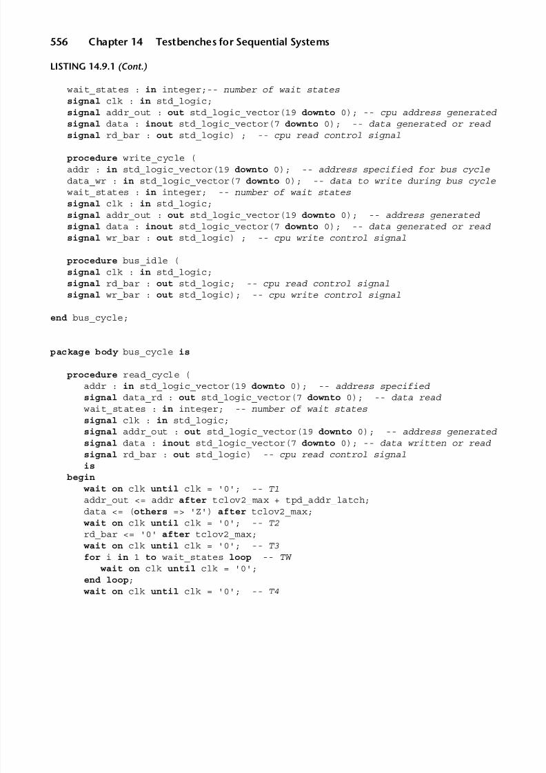
8/9/2019 VHDL for Engineers - Kenneth L. Short.pdf
http://slidepdf.com/reader/full/vhdl-for-engineers-kenneth-l-shortpdf 589/719
556 Chapter 14 Testbenches for Sequential Systems
LISTING 14.9.1 (Cont.)
wait_states : in integer;-- number of wait statessignal clk : in std_logic;signal addr_out : out std_logic_vector(19 downto 0); -- cpu address generated signal data : inout std_logic_vector(7 downto 0); -- data generated or read signal rd_bar : out std_logic) ; -- cpu read control signal
procedure write_cycle (addr : in std_logic_vector(19 downto 0); -- address specified for bus cycledata_wr : in std_logic_vector(7 downto 0); -- data to write during bus cyclewait_states : in integer; -- number of wait statessignal clk : in std_logic;signal addr_out : out std_logic_vector(19 downto 0); -- address generated signal data : inout std_logic_vector(7 downto 0); -- data generated or read signal wr_bar : out std_logic) ; -- cpu write control signal
procedure bus_idle (signal clk : in std_logic;signal rd_bar : out std_logic; -- cpu read control signalsignal wr_bar : out std_logic); -- cpu write control signal
end bus_cycle;
package body bus_cycle is
procedure read_cycle (addr : in std_logic_vector(19 downto 0); --
address specified signal data_rd : out std_logic_vector(7 downto 0); -- data read wait_states : in integer; -- number of wait statessignal clk : in std_logic;signal addr_out : out std_logic_vector(19 downto 0); -- address generated signal data : inout std_logic_vector(7 downto 0); -- data written or read signal rd_bar : out std_logic) -- cpu read control signalis
begin
wait on clk until clk = '0'; -- T1addr_out <= addr after tclov2_max + tpd_addr_latch;data <= (others => 'Z') after tclov2_max;
wait on clk until clk = '0'; -- T2rd_bar <= '0' after tclov2_max; wait on clk until clk = '0'; -- T3for i in 1 to wait_states loop -- TW wait on clk until clk = '0';
end loop; wait on clk until clk = '0'; -- T4

8/9/2019 VHDL for Engineers - Kenneth L. Short.pdf
http://slidepdf.com/reader/full/vhdl-for-engineers-kenneth-l-shortpdf 590/719
Section 14.9 Bus Functional Models 557
data_rd <= data;rd_bar <= '1' after tclov2_min; wait on clk until clk = '1';addr_out <= (others => 'X') after tclov2_min + tpd_addr_latch;
end read_cycle;
procedure write_cycle (addr : in std_logic_vector(19 downto 0); -- address specified data_wr : in std_logic_vector(7 downto 0); -- data to writewait_states : in integer; -- number of wait statessignal clk : in std_logic;signal addr_out : out std_logic_vector(19 downto 0); -- address generated signal data : inout std_logic_vector(7 downto 0); -- data writen or read signal wr_bar : out std_logic) -- cpu write control signalis
begin
wait on clk until clk = '0'; -- T1addr_out <= addr after tclov2_max + tpd_addr_latch;data <= (others => 'Z') after tclov2_max; wait on clk until clk = '0'; -- T2data <= data_wr after tclov2_max;wr_bar <= '0' after tclov2_max; wait on clk until clk = '0'; -- T3for i in 1 to wait_states loop -- TW wait on clk until clk = '0';
end loop; wait on clk until clk = '0'; -- T4wr_bar <= '1' after tclov2_min; wait on clk until clk = '1';addr_out <= (others => 'X') after tclov2_min + tpd_addr_latch;data <= (others => 'Z') after tclov2_min;
end write_cycle;
procedure bus_idle (signal clk : in std_logic;signal rd_bar : out std_logic; -- cpu read control signalsignal wr_bar : out std_logic) -- cpu write control signalis
begin
wait on clk until clk = '0'; -- T idlerd_bar <= '1' after tclov2_max;wr_bar <= '1' after tclov2_max; wait on clk until clk = '1';
end bus_idle;
end bus_cycle

8/9/2019 VHDL for Engineers - Kenneth L. Short.pdf
http://slidepdf.com/reader/full/vhdl-for-engineers-kenneth-l-shortpdf 591/719

8/9/2019 VHDL for Engineers - Kenneth L. Short.pdf
http://slidepdf.com/reader/full/vhdl-for-engineers-kenneth-l-shortpdf 592/719
Section 14.9 Bus Functional Models 559
After the falling edge of the clock in T1, addr_out and data are assignedvalues. Signal addr_out is assigned addr, the address value passed to theprocedure in the call statement. This assignment is made with a delay of tclov2_max + tpd_addr_latch. Choosing tclov2_max causes the address toappear as late as possible in the bus cycle, which is the worst case. Delay
tpd_addr_latch is the delay of the address latch used to demultiplex theaddress/data bus in an 80C188EB CPU design.
State T2 After the falling edge of the clock in T2, rd_bar is asserted:
wait on clk until clk = '0'; -- T2rd_bar <= '0' after tclov2_max;
States T3 and TW After the falling edge of the clock in T3, the procedure uses a loop to insert thespecified number of wait states. This number is passed to the procedure in the call
statement as integer parameter wait_states:
wait on clk until clk = '0'; -- T3for i in 1 to wait_states loop -- TW
wait on clk until clk = '0';end loop;
If a 0 is passed as the actual value for the number of WAIT states, no WAIT statesare inserted in the bus cycle. No signals driven by the BFM change their valuesduring either T3 or TW.
State T4 After the falling edge of the clock in T4, the procedure reads the data and rd_bar isunasserted. In the second half of T4 at the rising edge of the clock, the address isassigned the unknown value:
wait on clk until clk = '0';-- T4data_rd <= data;rd_bar <= '1' after tclov2_min; wait on clk until clk = '1';addr_out <= (others => 'X') after tclov2_min + tpd_addr_latch;
Write Bus CycleBFM Waveforms
The overall design of the write_cycle procedure is similar to that of theread_cycle procedure. The major difference is that the BFM drives the data buswith a data value passed as a parameter. This data is driven on the bus at thebeginning of T2 and removed at the beginning of T4. In addition, for a write buscycle, wr_bar is asserted rather than read_bar.
The waveforms generated by a single call to the procedure write_cycle areshown in Figure 14.9.5.

8/9/2019 VHDL for Engineers - Kenneth L. Short.pdf
http://slidepdf.com/reader/full/vhdl-for-engineers-kenneth-l-shortpdf 593/719
560 Chapter 14 Testbenches for Sequential Systems
This call was made with an address parameter of 08000 hexadecimal and a datavalue of 80 hexadecimal. The write cycle in this figure is bounded by the waveformeditor cursors.
Sequencing BusCycles
Another advantage of a BFM model over a fully functional RTL model is that it is easyto directly create any desired sequence of bus cycles by simply calling bus cycle proce-dures in the desired order. In contrast, using a fully functional RTL model requireswriting and compiling CPU code to produce the desired bus cycles and loading thiscode into a memory model also connected to the CPU bus in the testbench.
An example of a sequence of calls to the bus cycle procedures to verify the pulsewidth modulated signal generator UUT is given in the next section.
14 .1 0 RE S PON S E MO NI TO RS
Testbenchfor PWMSG
A separate process can be used to monitor output responses from a UUT. A diagramof a testbench that uses a CPU BFM to write duty cycle values to the microprocessor-compatible PWMSG UUT in Section 9.6 is given in Figure 14.10.1. The testbenchcomponents, processes, and procedures are linked by signals.
The reset and clock are described by concurrent signal assignment statements.The CPU BFM is implemented using the package bus_cycle from the previoussection. Responses from the UUT are monitored by a separate response monitorprocess. The testbench is given in Listing 14.10.1.
The stimulus process contains a loop that calls procedure write_cycle. Eachcall loads a new value to produce a different duty cycle. The PWMSG is allowed togenerate each duty cycle for 10 ms before the next duty cycle value is loaded.
FIGURE 14.9.5
Waveforms produced by a call to the write_cycle procedure at time = 1000 us.

8/9/2019 VHDL for Engineers - Kenneth L. Short.pdf
http://slidepdf.com/reader/full/vhdl-for-engineers-kenneth-l-shortpdf 594/719
Section 14.10 Response Monitors 561
The process stimuli was written to show that it is not difficult to write an exhaustiveverification for this UUT. However, running the exhaustive verification takes arelatively long time. It may be preferable to simply have a limited number of calls toprocedure write_cycle to verify a select number of duty cycle values. For example,a sufficient set of load values might be x"00", x"01", x"08", x"7F", x"80", x"FE",and x"FF".
LISTING 14.10.1Testbench for pulse width modulated signal generator.
library ieee;use ieee.std_logic_1164.all;use ieee.numeric_std.all;
library bus_cycle;use bus_cycle.bus_cycle.all;
entity pwm_tb is
end pwm_tb;
architecture tb_architecture of pwm_tb is
constant cpu_clk_period : time := 125 ns;
-- Stimulus signalssignal pwm_out: std_logic;
-- Observed signalssignal d : std_logic_vector(7 downto 0);
(Cont.)
FIGURE 14.10.1
Testbench structure for PWMSG using CPU BFM.
PWM Model8
CPU BFMStimuli
Monitor
data
cs_bar
we_bar
pwm_out
reset clock reset clock reset clock
reset clock

8/9/2019 VHDL for Engineers - Kenneth L. Short.pdf
http://slidepdf.com/reader/full/vhdl-for-engineers-kenneth-l-shortpdf 595/719
562 Chapter 14 Testbenches for Sequential Systems
LISTING 14.10.1 (Cont.)
signaladdr_cpu: std_logic_vector (19 downto 0);signaldata_cpu: std_logic_vector (7 downto 0);signalwr_bar_cpu: std_logic;signalrd_bar_cpu: std_logic;signalclkout: std_logic := '0';
signal cpu_reset_bar : std_logic;signal cpu_reset : std_logic;signal duty_cyc_ld : std_logic_vector(7 downto 0);
begin
-- Unit Under Test port mapUUT : entity pwmport map (
data => data_cpu,
cs_bar => '0',we_bar => wr_bar_cpu,clk => clkout,reset => cpu_reset,pwm_out => pwm_out);
cpu_clock_gen : clkout <= not clkout after cpu_clk_period/2;
cpu_reset_gen : cpu_reset_bar <= '0', '1' after 2 * cpu_clk_period;
cpu_reset <= not cpu_reset_bar;
stimulus : process
begin
rd_bar_cpu <= '1';wr_bar_cpu <= '1'; wait for 1 ms;for i in 0 to 255 loop
duty_cyc_ld <= std_logic_vector(to_unsigned(i,8));write_cycle(x"08000", duty_cyc_ld, 0, clkout, addr_cpu, data_cpu,wr_bar_cpu); wait for 10 ms;
end loop; wait;
end process;
monitor: process
variable leading_edge, high_time, pulse_period: time;

8/9/2019 VHDL for Engineers - Kenneth L. Short.pdf
http://slidepdf.com/reader/full/vhdl-for-engineers-kenneth-l-shortpdf 596/719
Section 14.10 Response Monitors 563
variable data_written : unsigned(7 downto 0);variable duty_cycle_set, duty_cycle_meas : integer;
begin
wait until rising_edge(wr_bar_cpu);data_written := unsigned(data_cpu); wait until pwm_out = '1'; -- skip first pulse wait until pwm_out = '1';leading_edge := now; wait until pwm_out = '0';high_time := now - leading_edge; wait until pwm_out = '1';pulse_period := now - leading_edge;duty_cycle_set := 100 * (to_integer(data_written))/255;duty_cycle_meas := (100 * high_time)/pulse_period;if duty_cycle_set > 1 and duty_cycle_set < 100 then
assert duty_cycle_meas <= duty_cycle_set + 1and duty_cycle_meas >= duty_cycle_set - 1
report "duty cycle error" & CR & LF &"iteration = " & integer'image(to_integer(unsigned(duty_cyc_ld))) &CR
& LF &"duty cycle set = " & integer'image(duty_cycle_set) &CR & LF &"duty cycle measured = " & integer'image(duty_cycle_meas);
end if;end process;
end tb_architecture;
The monitor process waits for the rising edge of the wr_bar_cpu signal,
which indicates that the BFM has written a new value to the PWMSG. Themonitor process then waits until the second positive edge of the PWMSGpwm_out output. The first transition of pwm_out is skipped, because writing anew value to the PWMSG by the microprocessor is not synchronized with thepulse currently being generated by the PWMSG and may, therefore, not have therequired duty cycle.
Now The second output pulse’s high-time duration and period are measured usingVHDL’s now function. Function now is provided by package STANDARD. Thisfunction returns the current simulation time, Tc. Current simulation time values are
of subtype delay_length.From the values returned by now, the measured duty cycle is computed. Thespecified duty cycle is computed from the value that was written to the PWMSG bythe microprocessor. An assertion statement compares the measured duty cycle withthe specified duty cycle. The measured duty cycle has to be within ± 1 percent of thespecified duty cycle or a report of the difference is made.

8/9/2019 VHDL for Engineers - Kenneth L. Short.pdf
http://slidepdf.com/reader/full/vhdl-for-engineers-kenneth-l-shortpdf 597/719
564 Chapter 14 Testbenches for Sequential Systems
PROBLE MS
14.1 What two stimulus signals are always required in a testbench for a synchronous system? Whatis the basic criterion for these signals?
14.2 If period is an odd number, what is the effect on the actual period of a clock generated by
the statement:
clk <= not clk after period/2;
In other words, is the result from the division truncated, resulting in a shorter period, orrounded up, resulting in a longer period? If period is 15 ns, can the above statement be rewrittento produce a more accurate clock model? What effect does simulator resolution have on thisaccuracy?
14.3 Can a clock with other than a 50% duty cycle be generated using a concurrent signal assignmentstatement? If so, write a concurrent signal assignment statement to generate a clock with a 40%duty cycle. If not, explain why.
14.4 Can a concurrent signal assignment statement describe a clock that is stopped by a booleansignal? If so, write such a statement that describes a clock with a 50% duty cycle that is stoppedwhen the boolean signal end_sim becomes true. If not, explain why.
14.5 The examples of clocks generated by processes in Section 14.2 used loops. Consider thefollowing attempt to describe a clock:
clock : processbegin
clk <= '0';wait for period/2;clk <= '1';
wait for period/2end process;
(a) Explain why this code either does or does not successfully describe a clock waveform.(b) If the code does successfully describe a clock waveform, can anend_sim signal be added
to the process to end the simulation? If so, write the modified code.
14.6 Write a procedure named clk_gen that has the following declaration:
procedure clk_gen (constant freq, duty_cycle : in real;signal clk : out std_logic);
where the frequency is specified in MHz and the duty cycle is a value between 0.0 and 1.0. Thisprocedure must be written to allow any frequency and duty cycle to be specified when theprocedure is called.
14.7 A UUT requires a reset pulse named rst that is asserted high for 250 ns at power up and isthen unasserted. Write a concurrent signal assignment statement to generate rst.
14.8 It is often useful to have code for a reset and a clock that can be reused when we want to quicklyverify UUTs, such as simple counters, by examining their output waveforms. Write a procedure

8/9/2019 VHDL for Engineers - Kenneth L. Short.pdf
http://slidepdf.com/reader/full/vhdl-for-engineers-kenneth-l-shortpdf 598/719
Problems 565
that can be called concurrently that has five parameters passed to it: clock period, asserted stateof the reset, duration of the reset as a number of clock cycles, initial level of the clock, and numberof clock cycles to be generated after the reset is unasserted. The values returned by the procedureare the signals reset and clk.
14.9 Explain why the following statement is valid for the positive-edge-triggered flip-flop in Listing
8.4.5. For a functional simulation, the D input can be changed to the next input value as late assimultaneously with the clock edge. That is, if a new value is assigned to D in the same deltacycle that the clock makes its 0 to 1 transition, the value stored in the D flip-flop will be thenew value assigned to D, not its old value. Use the diagram in Figure 6.6.1 as the basis for yourexplanation.
14.10 Write a testbench for the 4-bit right shift register in Listing 9.2.1. Use vectors to provide theserial input data stimulus and the expected serial output value.
14.11 Write a testbench for the 4-bit binary counter in Listing 9.4.1.
14.12 Write a testbench for the 12-bit binary counter in Listing 9.4.4.
14.13 Write a testbench for the modulo 32 BCD counter in Listing 9.4.7.
14.14 Write a testbench for the positive edge detector in Listing 9.5.1.
14.15 Write a testbench for the single shot in Listing 9.5.2.
14.16 Generate the stimulus in Figure 14.6.2 using four concurrent signal assignment statementseach with multiple after clauses.
14.17 Generate the stimulus in Figure 14.6.2 using a process with signal assignment statements andwait for statements.
14.18 Write a package named signal_probe and its associated package body. This packagecontains a single procedure named period_probe, which has the following proceduredeclaration:
procedure period_probe (signal a : in std_logic; signal period : out time);
Procedure period_probe computes the period of the signal passed to it as parameter a.This procedure is to be called as a concurrent procedure. Once called, this procedure neverreturns. However, its parameter period provides a running measurement of the period of a.Write this procedure to take advantage of the predefined function now in making itscomputation.
Procedure period_probe could be used during functional simulation of a structural styledesign. Multiple concurrent calls to procedure period_probe would provide simultaneousmeasurements of the periods of multiple signals in the design. The signals that appear as theactual parameters replacing parameter period in the calls could be viewed on the simulation
waveforms to see the period values. The procedure calls would be removed before the designis synthesized.

8/9/2019 VHDL for Engineers - Kenneth L. Short.pdf
http://slidepdf.com/reader/full/vhdl-for-engineers-kenneth-l-shortpdf 599/719
566
Chapter 15
Modular Design and Hierarchy
A large complex system is impossible to comprehend, design, or verify as a singleentity. Traditionally, in both hardware and software design, a complex system ispartitioned into modules for the purposes of documentation, design, coding, verifi-cation, and maintenance. During the partitioning process, each module’s interfaceand function are completely defined, so that when the modules are interconnectedthey accomplish the system’s overall function.
With each module’s interface and function completely defined, each can beindependently designed and verified. This reduces the overall complexity of systemdesign and verification. In VHDL, modules are implemented as design entities. Theyare stored in libraries for use in current designs and reuse in future designs.
VHDL provides constructs that support modular design of complex systems.These constructs and their use are discussed in this chapter.
1 5. 1 MO DU LA R DE SI GN , PA RT IT IO NI NG, AN D HIE RARC HY
Modular Design Modular design is a long-established methodology for designing complex hardware
or software systems. In modular design, a complex system is partitioned into simplermodules. These modules are interconnected to accomplish the complex system’soverall function.
Each module’s particular task or function is defined in a way that allows themodule to be independently designed and verified, before being combined with theother modules. Designing and verifying each module independently allows us tofocus on one module at a time, simplifying the overall design effort.

8/9/2019 VHDL for Engineers - Kenneth L. Short.pdf
http://slidepdf.com/reader/full/vhdl-for-engineers-kenneth-l-shortpdf 600/719
Section 15.1 Modular Design, Partitioning, and Hierarchy 567
For software modules to be independently designed and verified, they must becapable of being independently compiled. The same is true for hardware modulesdescribed in VHDL. Once verified and properly documented, a module can beplaced in a library and used in the original and subsequent designs.
Flat Partitions In order to take advantage of VHDL’s constructs that support modular design, adesign must first be partitioned into modules. If a complex system is partitioned intoa set of interconnected modules and none of these modules is further partitioned, theresult is a flat or single-level partition.
HierarchicalPartitions
For many complex designs a flat partition is not sufficient, because some of themodules are still too complex. Accordingly, each complex module is further parti-tioned into simpler modules. This creates a hierarchical (multilevel) partition of thesystem.
Top-Down Design Hierarchical partitioning is the basis of top-down design. In top-down design, asystem’s total function is repeatedly partitioned into simpler modules from the toplevel down.
The top-level partition (first-level partition) in a hierarchy constrains all subse-quent (lower-level) partitions (Figure 15.1.1). As a result, the top-level partition isparticularly important, since it defines and constrains the system’s overall archi-tecture and implementation.
Each module in the top-level partition may itself be partitioned to further reduce itscomplexity, creating the next lower-level partition. The resulting hierarchy of modulescan be represented by a hierarchical block diagram or a hierarchy tree (Figure 15.1.1).
A hierarchy tree clearly represents the hierarchical relationship of a system’s modules.The modules at the bottom of each branch of a hierarchy tree are called leaf nodes.
FIGURE 15.1.1
Hierarchy tree for the modular partition of a complex system.
top level
1st-levelpartition
2nd-levelpartition
3rd-levelpartition

8/9/2019 VHDL for Engineers - Kenneth L. Short.pdf
http://slidepdf.com/reader/full/vhdl-for-engineers-kenneth-l-shortpdf 601/719
568 Chapter 15 Modular Design and Hierarchy
As a very simple example of a hierarchical partition, consider the partition of a
full adder. A hierarchy tree representing such a partition is given in Figure 15.1.2.Typically, the top-level partition consists of the modules that would comprise theblocks in a top-level block diagram of the system. For example, compare themodules in Figure 15.1.2 to the blocks in the block diagram in Figure 2.9.1. It isobvious from both the block diagram and hierarchy tree that some of the samemodules are used multiple times in the partition.
The partitioning process is continued until each leaf node represents a relativelysimple module that we can easily comprehend and directly code. For example, theXOR gate function can be simplified by further partitioning, as in Figure 15.1.3.
For more experienced VHDL designers, what is considered simple enough todirectly code is a lot more complex than it is for beginning designers. So, as we gain
more experience in coding VHDL, we are likely to have more complex leaf nodes.However, there are other tradeoffs in deciding the complexity of leaf nodes, such ascode readability and maintainability, module reuse, and synthesis efficiency.
Bottom-UpImplementation
Modules corresponding to leaf nodes are coded and verified first. These modules arethen interconnected using structural style descriptions to form modules on the next
FIGURE 15.1.2
Hierarchy tree for a full adder.
Full Adder
Half Adder Half Adder OR Gate
AND Gate XOR Gate AND Gate XOR Gate
FIGURE 15.1.3
Hierarchy tree for XOR gate.
XOR Gate
NOT Gate NOT Gate AND Gate AND Gate OR Gate

8/9/2019 VHDL for Engineers - Kenneth L. Short.pdf
http://slidepdf.com/reader/full/vhdl-for-engineers-kenneth-l-shortpdf 602/719
Section 15.1 Modular Design, Partitioning, and Hierarchy 569
higher level. This process is repeated for each higher-level partition until the top-levelpartition is implemented. This approach comprises a bottom-up implementation.
Balanced Hierarchy Modules at the same level in a hierarchy should have a relatively comparable degreeof complexity. The number of modules in each hierarchical level should strike abalance between producing an overly horizontal or an overly vertical partition. Ahorizontal partition is one that has a large number of modules in the top-levelpartition and few levels. A vertical partition has few modules at each level and alarge number of levels. Either extreme is more difficult to comprehend than is abalanced hierarchy.
Advantages ofa Good DesignPartition
Effort expended in creating a good design partition is well rewarded. A good partitionprovides several advantages:
• Design management is easier
• Modules can be designed and verified by different individuals• Maximum reuse of modules is made possible
• The design description is more readable and easier to comprehend
• Verification is simplified
• Better design results are likely
• The portability of the design is enhanced
Criteria forDelineating
Modules
The function(s) realized by a module should be logically coherent. Only relatedfunctionality should be contained in a single module.
Each module should have a relatively small number of well-defined inputs andoutputs. Definition of a module should also consider its likelihood of being reusable,either in the current design or subsequent designs. Reusability is important, sincemodule reuse provides significant design and verification productivity gains.
While we want to limit the complexity of the leaf node modules so they aresimple enough to directly code, we don’t want to make them too simple. The simplerthey are, the more of them that will be required. Since modules are interconnectedusing a structural style description; use of very low logical complexity modulesresults in an inefficient and overly complex structural description. The ultimateexample of this inefficiency is the implementation of a complex design using onlymodules that are two-input NAND gates.
Bottom-UpVerification
Each module should be defined so that it is individually verifiable. Each module isindependently verified before being combined with other modules to form a higher-level module. Higher-level modules are independently verified before beingcombined to form the complete system. The complete system is then verified. Thisapproach is called bottom-up verification.

8/9/2019 VHDL for Engineers - Kenneth L. Short.pdf
http://slidepdf.com/reader/full/vhdl-for-engineers-kenneth-l-shortpdf 603/719
570 Chapter 15 Modular Design and Hierarchy
Creating a Partition Partitioning is an art. The ability to create good partitions improves with experience.In the past, when medium-scale integration (MSI) was the most complex level of ICavailable, designers partitioned their designs to take maximum advantage of available MSI functions. At that time, this approach minimized system cost byreducing package count and increasing the reliability.
As a result, decoder, encoder, multiplexer, register, shift register, counter, adder,and other common MSI functions became the elemental functions used to implementcomplex systems.
Designers using PLDs aren’t restricted to the same functions that existed whenusing MSI. However, functions similar to the “elemental functions” from MSIdesign are still often the basis for lower-level partitions.
Partitioning andDesign Reuse
If we can partition a system to make use of existing modules, design time is signifi-cantly reduced. Reused modules may be ones that we have created for prior designsor that we have obtained from others, possibly in the form of intellectual property
(IP). Reuse of modules increases a system’s reliability, assuming a reused module isone that has been verified and proven in a previous design.
Today, the significant advantages of design reuse often lead to defining each moduleof a partition in a somewhat more general and flexible way than is required for a specificdesign. This improves the likelihood that modules are reusable in other designs.
Partitions Basedon Data Pathand Control
A top-level partition of hardware into one or more data paths and control modules(“System Architecture” on page 441) is often made. Recall that a data path consistsof registers separated by combinational arithmetic or logic processing modules. Asequential control module (a FSM) provides control signals to enable registers and to
control the operation of the arithmetic and logic modules.
Partitions Basedon a PLD Vendor’sLibraries
Ideally, we want our VHDL design descriptions to be portable, so that any targetPLD with sufficient logic capacity can be used to realize a system. As a result, wegenerally want our partitions to be independent of special architectural features of aparticular PLD.
Nevertheless, to achieve very high system performance, it is sometimes necessaryto take advantage of optimized vendor library modules associated with a specifictarget PLD’s architecture. In such cases, we must create a partition that includesmodules from the vendor’s library. The result is a design that is not portable.
However, if these vendor modules are isolated and limited to the higher-levelpartitions, they can be replaced by equivalent modules if we must change the targetPLD. Thus, we can still maintain a degree of portability.
Design Entitiesas Modules
In VHDL, design entities serve the purpose of modules. Structural style descriptionsdescribe how particular design entities are interconnected to form a more complexsystem.

8/9/2019 VHDL for Engineers - Kenneth L. Short.pdf
http://slidepdf.com/reader/full/vhdl-for-engineers-kenneth-l-shortpdf 604/719
Section 15.2 Design Units and Library Units 571
1 5. 2 D ES IG N U NI TS AN D L IBR AR Y U NI TS
VHDL provides many features that support creating and managing modular designs.Important among these are library units.
As discussed in Section 2.9, each design entity can be described in a separate file.Using separate files provides a degree of modularity that makes design managementeasier because each file is smaller, improving the readability of its code. Usingseparate files also allows separate compilation and verification of each design entity.Beyond simply allowing a complex design to be divided into multiple files, VHDLprovides more extensive features for facilitating design modularity.
Design Units One feature associated with independent compilation is that of a design unit. A design
unit is a VHDL construct that can be independently compiled and stored in a designlibrary. Design units provide modularity for the design management of complex
systems.
Design Files A design file is a source file containing one or more design units (Figure 15.2.1). Adesign file is the input to a VHDL compiler. Design units in a design file arecompiled in the same order as their textual order in the file.
FIGURE 15.2.1
Design file and design units.
design unit
design unit
design unit
Design File
contextclause
libraryunit
Design Unit
primary units: entity declaration package declaration configuration declaration
secondary units: architecture body package body

8/9/2019 VHDL for Engineers - Kenneth L. Short.pdf
http://slidepdf.com/reader/full/vhdl-for-engineers-kenneth-l-shortpdf 605/719
572 Chapter 15 Modular Design and Hierarchy
Library Units A design unit is comprised of a context clause and a library unit, as shown in Figure15.2.1. Compilation of a design unit defines the corresponding library unit thatresides in a design library. That is, a library unit is the compiled and stored form of adesign unit.
There are five kinds of library unit s. They are divided into two groups, primary
units and secondary units. The primary units are:
• Entity declaration
• Package declaration
• Configuration declaration
A primary unit describes an external view or interface to either an entity, package,or configuration.
The secondary units are:
• Architecture body
• Package body
Note that while the LRM defines entity declarations, package declarations, config-uration declarations, architecture bodies, and package bodies syntactically as libraryunits, much of the literature on VHDL refers to them, informally, as design units. Ineffect, the terms library unit and design unit are often used interchangeably.
A secondary unit describes the behavior or structure of its associated primaryunit. Of the secondary units, only architecture bodies have unique names. A packagebody has the same name as its associated package declaration. A primary unit mustbe compiled before any associated secondary unit is compiled. A secondary unitmust be compiled into the same library as its associated primary unit.
The relationship between a package declaration and its associated package bodyis similar to the relationship between an entity declaration and its associated archi-tecture body. The primary unit describes the interface, and the secondary unitdescribes the behavior or structure. However, there can be only one package body foreach package declaration, whereas an entity declaration can have multiple archi-tecture bodies.
An entity declaration and an associated architecture body are the only two libraryunits that must exist to form a design entity. Package declarations, package bodies,and configuration declarations are optional. All of the library units, except configu-ration declarations, have been discussed in previous chapters. Configuration declara-
tions are discussed later in this chapter.
Library Unit Names The names of primary units must be unique within a given library. Names of alter-native architectures associated with a given entity declaration must be unique.However, two architectures associated with different entities can have the samename. A package body’s name must be the same as its corresponding package.
8/9/2019 VHDL for Engineers - Kenneth L. Short.pdf
http://slidepdf.com/reader/full/vhdl-for-engineers-kenneth-l-shortpdf 606/719
Section 15.3 Design Libraries 573
15 . 3 D E S I GN L I BR A R I E S
A simulator can only simulate programs that have been successfully compiled andstored in a library. Accordingly, we have used libraries routinely in previous designs.
Libraries also provide features that support design management of complex systemsand facilitate design reuse.
A complex design will consist of a number of design units. Many of these designunits may need to declare the same constants, data types, and subprograms. Instead of having each design unit repeat the text for these shared declarations and subprogrambodies, they can be placed in packages and package bodies and compiled to a library.Each design unit can then reference the packages in this library to make use of theircontents.
Each design entity can be separately compiled and stored in a library. Otherdesign entities that need to instantiate previously compiled design entities as compo-nents can simply reference their libraries to do so.
Design Library A design library is a logical storage area in the host computer environment forcompiled design units (library units). Its physical structure is implementation dependentand not defined in the VHDL standard. For most host computer implementations, alibrary is simply a directory. Each VHDL compiler’s documentation must be consultedto determine the format and implementation of its libraries.
Library LogicalNames
A design library is identified by its logical name. We use this name to reference thelibrary in our VHDL descriptions. A path must be assigned to each logical library
name to point to the physical directory that contains the library. The way this is donedepends on the compiler. With some tools, this is done in an initialization file that wemust create. In most tools having an IDE, this assignment is made in a transparentfashion when we set up a new design project.
Working andResource Libraries
There are two kinds of design libraries: working library and resource library. Theworking library is the library into which the library unit resulting from compilationof a design unit is placed. We can specify into which library we want a design unit tobe compiled. If we do not specify a library, the design unit is compiled into thedefault library named work.
A resource library is a library containing library units that are referenced withinthe design unit being compiled. The logical names of the referenced libraries must belisted in a library clause(s) preceding each design unit.
While only one library can be the working library during a compilation, anarbitrary number of resource libraries, including the working library itself, may beused.

8/9/2019 VHDL for Engineers - Kenneth L. Short.pdf
http://slidepdf.com/reader/full/vhdl-for-engineers-kenneth-l-shortpdf 607/719
574 Chapter 15 Modular Design and Hierarchy
Library STD All VHDL compilers come with the Library STD included. This built-in library isprovided by IEEE Std 1076. Library STD contains two packages: STANDARD andTEXTIO. It is in package STANDARD that the predefined types and operators of VHDL are defined. This package was discussed in Chapter 13. Package TEXTIO
contains predefined types, functions, and procedures used for reading and writing files.
Library IEEE VHDL compilers also include the library IEEE. This library contains packages definedby VHDL’s supporting standards, such as packages STD_LOGIC_1164 andNUMERIC_STD. Most compiler vendors also include in this library other de factostandard packages such as STD_LOGIC_ARITH. These packages were also discussedin Chapter 13.
User-DefinedLibraries
Of course, we can write our own packages and place them in libraries that we create(user-defined libraries). We can also place design entities that we have created in ouruser-defined libraries. Placing subprograms and design entities in user libraries
allows us to easily reuse them in subsequent designs.
IntellectualProperty Libraries
Third-party intellectual property providers sell libraries containing complex designentities that we can use as modules in our designs.
PLD VendorLibraries
PLD vendors provide precompiled design entities optimized for the architecture of aparticular target PLD family. Entity and package declaration source code is providedwith these libraries. However, source code for the architecture bodies and packagebodies is usually not provided, only precompiled versions.
Also included in the VHDL compiler’s system libraries are libraries containing
the primitive component models used to functionally and physically model aparticular vendor’s PLD families. These models are used in post-synthesis andtiming simulations.
15 .4 US IN G LI B R AR Y UN IT S
To use a library unit in another design unit, we must specify where the library unit isto be found. Both the logical name of the resource library containing the library unitand the library unit’s name must be made visible to the design unit. This visibility
can be provided directly or by selection.Direct visibility of a library unit and its resource library is made possible by use
of a context clause.
Context Clause A design unit was defined as consisting of a context clause and a library unit. Thecontext clause, at the head of a design unit, defines the name environment in which adesign unit is compiled.

8/9/2019 VHDL for Engineers - Kenneth L. Short.pdf
http://slidepdf.com/reader/full/vhdl-for-engineers-kenneth-l-shortpdf 608/719
Section 15.4 Using Library Units 575
A context clause consists of a library clause and/or a use clause. For example,most of the design units in previous examples used signals and variables of typestd_logic and were preceded by the context clause:
library ieee;
use ieee.std_logic_1164.all;
Library Clause A library clause defines the logical names of design libraries that are visible to agiven design unit. The scope of a library clause starts immediately after the libraryclause and extends to the end of the declarative region of the design unit in which thelibrary clause appears. Within this scope, each library name defined by the libraryclause is directly visible.
Use Clause A use clause makes particular declarations in a library directly visible to the libraryunit it precedes. In the previous example, the keyword all makes all the declara-
tions in package STD_LOGIC_1164, in the library ieee, directly visible to thelibrary unit it precedes.
A name made directly visible to a primary library unit by a context clause is
automatically visible in any associated secondary library unit. As a result, a designlibrary made visible to an entity declaration is also visible to all its associated archi-tecture bodies.
For example, in Listing 2.6.1 there are two design units, the entity declarationhalf_adder and its associated architecture body dataflow2. The context clause atthe beginning of the program is associated with the entity declaration library unit.The architecture body does not require its own context clause, because it is
associated with the entity declaration half_adder, and every name made directlyvisible to half_adder is automatically visible to the architecture dataflow2,associated with half_adder.
In contrast, in Listing 2.9.1 the context clause preceding the entity declarationhalf_adder only applies to that entity declaration and its associated architecturebody dataflow. Entity declaration or_2 in the design file requires its own contextclause.
Library Units MadeVisible by Selection
Library units can also be made visible by selection; that is, by using a selected nameto reference the library unit instead of using a use clause. The selected name
specifies the library name and the library unit’s name. An appropriate library clauseis still required. An example of this is discussed in “Specifying the Library as Part of an Entity Name” on page 579.
Implicit ContextClause
Because almost every VHDL description needs to use types and operators frompackage STANDARD, the contents of this package are automatically made visible toall library units. This is done by the implicit context clause. Every library unit

8/9/2019 VHDL for Engineers - Kenneth L. Short.pdf
http://slidepdf.com/reader/full/vhdl-for-engineers-kenneth-l-shortpdf 609/719
576 Chapter 15 Modular Design and Hierarchy
(except package STANDARD itself) is assumed to be preceded by the implicitcontext clause:
library std, work;use std.standard.all;
This implicit context clause defines two libraries that can be referenced in anylibrary unit without requiring the use of an explicit context clause. The use clausemakes all of the declarations in package STANDARD, in the library STD, directlyvisible to the design unit.
Library Work The second library defined by the implicit context clause is the working library. Thisis the library to which any design unit is, by default, compiled. The logical namework can be used to reference the working library, regardless of the actual logicalname of this library. Tools that allow us to create designs as projects may use theproject name as an alias for the library work. When this is the case, we can refer to
the working library by either name.
Organizing DesignUnits into DesignFiles
If an entity declaration and its associated architecture body are in separate design files,each requires a copy of the context clause. This allows each library unit to be indepen-dently compiled. The order of compilation is important; we must compile the entitydeclaration (primary unit) before its associated architecture body (secondary unit).
Since multiple design units in a single design file are compiled in the order of their textual occurrence, design units must be properly ordered in the file. Eachprimary design unit must precede any associated secondary design unit.
There are two rules that govern the order of compilation of a design unit:
1. A primary unit whose name is referenced within a given design unit must becompiled prior to compiling the given design unit.
2. A primary unit must be compiled prior to compiling any associated secondaryunits.
User written packages and other design units can be precompiled and placed in aresource library. Design entities in a resource library can be used as modules bydesign entities in a design file. The appropriate context clauses for any resourcelibraries used must be included prior to each library unit in a design file.
Compilation Orderfor Separate Files An organization of design units that is appropriate to complex designs and to designsdeveloped by groups of engineers uses multiple design files. As seen previously, thefull-adder design could be separated into three design files: one for the half adder,one for the OR gate, and one for the top-level entity.
These separate design files have to be compiled in the appropriate order. If entitydeclarations and architecture bodies are placed in separate design files and there aremultiple architecture bodies for a single entity declaration, then the desired archi-tecture body must be compiled last, or a configuration declaration must be used.

8/9/2019 VHDL for Engineers - Kenneth L. Short.pdf
http://slidepdf.com/reader/full/vhdl-for-engineers-kenneth-l-shortpdf 610/719
Section 15.5 Direct Design Entity Instantiation 577
1 5. 5 D IR EC T D ES IG N E NT IT Y I NS TA NT IA TI ON
Modular and hierarchical designs are implemented in VHDL using structural stylearchitectures. A structural architecture is, ultimately, a collection of design entities
interconnected by signals.
Closer Look atStructural Design
In a structural style description, component instantiation statements are used tocreate an instance of each design entity. A simplified syntax for a component instan-tiation statement was introduced in Chapter 2 in Figure 2.6.2.
The syntax in Figure 2.6.2 provides two forms for a component instantiationstatement. The first form is for direct instantiation of a design entity. The secondform is for indirect instantiation. Indirect instantiation instantiates a component,which serves as a placeholder for a design entity rather than directly instantiating adesign entity. The binding of each component to an actual design entity is then accom-
plished using either default binding or an explicit binding indication.
Direct Design EntityInstantiation
Using direct design entity instantiation, a component instantiation statement directlyspecifies the name of the design entity and, optionally, the name of the associatedarchitecture body. The statement’s port map specifies how each port of this instanceof the design entity is either connected to a signal in the enclosing architecture bodyor an expression, or is left unconnected (using the open keyword).
Consider the following example. Assume that we have created separate designfiles for each of the following entity declarations and architecture bodies andcompiled them into our working library in the order listed:
• Entity and_2
• Architecture dataflow of and_2
• Architecture behavioral of and_2
• Entity or_2
• Architecture dataflow of or_2
We now want to use these entity declarations and architecture bodies in a struc-tural style description of the simple combinational circuit in Figure 15.5.1. Thedescription is given in Listing 15.5.1.
This description contains three component instantiation statements. Each onespecifies the direct instantiation of a design entity. Two copies of the and_2 designentity and one copy of the or_2 design entity are instantiated.
The port maps specify how each design entity’s ports are connected to the signalsof architecture structural_1. Each association element in the port map consists of a design entity port name to the left of the arrow symbol ( =>) and a signal of theenclosing architecure to the right. Port maps were previously discussed in the section“Port Map” on page 61.
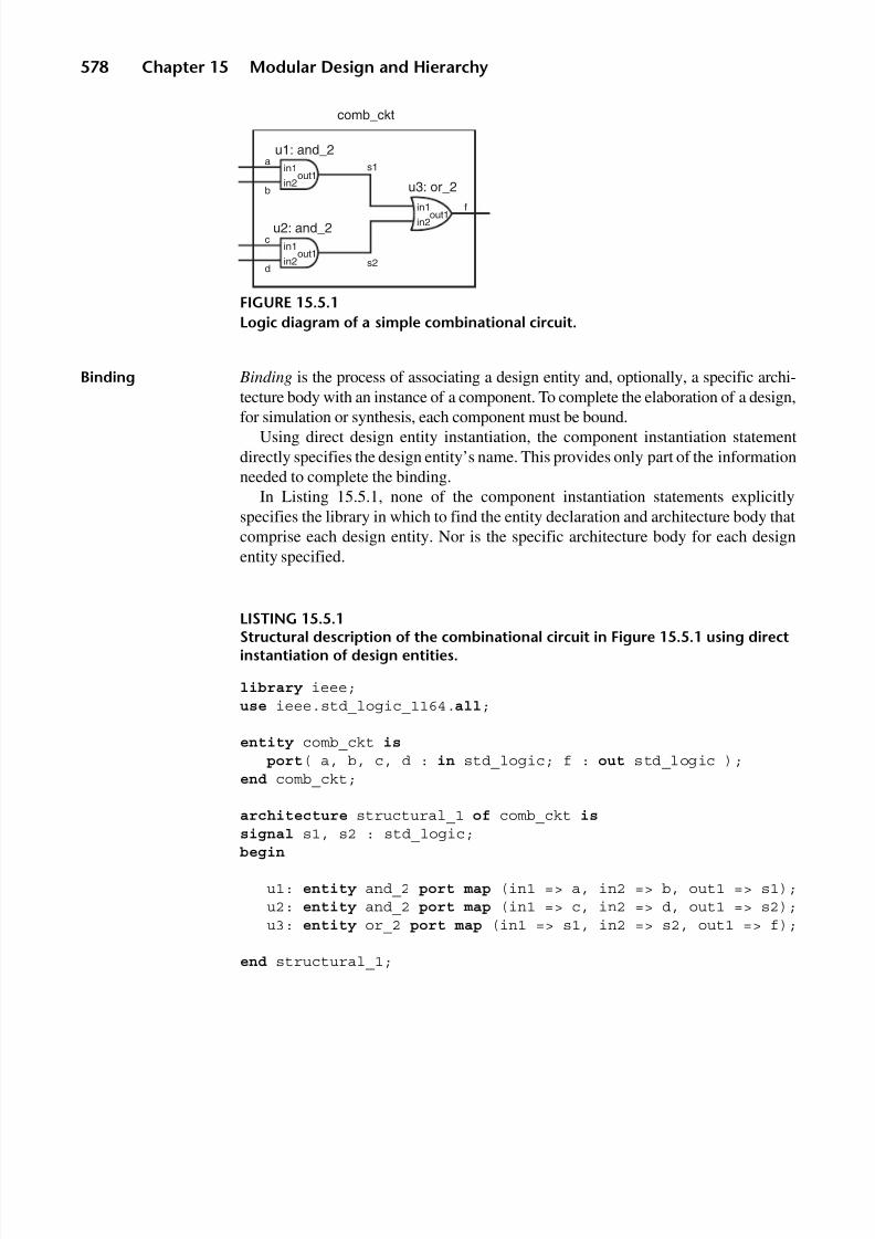
8/9/2019 VHDL for Engineers - Kenneth L. Short.pdf
http://slidepdf.com/reader/full/vhdl-for-engineers-kenneth-l-shortpdf 611/719
578 Chapter 15 Modular Design and Hierarchy
Binding Binding is the process of associating a design entity and, optionally, a specific archi-tecture body with an instance of a component. To complete the elaboration of a design,
for simulation or synthesis, each component must be bound.Using direct design entity instantiation, the component instantiation statement
directly specifies the design entity’s name. This provides only part of the informationneeded to complete the binding.
In Listing 15.5.1, none of the component instantiation statements explicitlyspecifies the library in which to find the entity declaration and architecture body thatcomprise each design entity. Nor is the specific architecture body for each designentity specified.
LISTING 15.5.1Structural description of the combinational circuit in Figure 15.5.1 using directinstantiation of design entities.
library ieee;use ieee.std_logic_1164.all;
entity comb_ckt is
port( a, b, c, d : in std_logic; f : out std_logic );end comb_ckt;
architecture structural_1 of comb_ckt is
signal s1, s2 : std_logic;begin
u1: entity and_2 port map (in1 => a, in2 => b, out1 => s1);u2: entity and_2 port map (in1 => c, in2 => d, out1 => s2);u3: entity or_2 port map (in1 => s1, in2 => s2, out1 => f);
end structural_1;
FIGURE 15.5.1
Logic diagram of a simple combinational circuit.
in1
in2
in1
in2
out1
in1in2
out1
s1
s2
u1: and_2
comb_ckt
u3: or_2
a
b
out1
u2: and_2c
d
f

8/9/2019 VHDL for Engineers - Kenneth L. Short.pdf
http://slidepdf.com/reader/full/vhdl-for-engineers-kenneth-l-shortpdf 612/719
Section 15.5 Direct Design Entity Instantiation 579
Default BindingRules
The compiler can follow a set of default binding rules, defined in the LRM, to accom-plish bindings. For example, since no library is specified in Listing 15.5.1, by defaultthe compiler looks in the working library (work) for an entity declaration whose entityname and interface match those specified in the component instantiation statement. If,in the working library, there is more than one architecture body associated with that
entity declaration, then the compiler uses the one most recently compiled.
MatchingInterfaces
For the purposes of default binding, the interface of a design entity in a librarymatches that of the design entity in a component instantiation statement, if thegenerics and ports have the same names and the modes and types of these genericsand ports are appropriate for the association.
For entity and_2 in Listing 15.5.1, there are two possible architectures: dataflowand behavioral. Assuming that behavioral was the most recently compiled,instances u1 and u2 will both use that architecture body. There is only one architecturein the working library for or_2, so there is no choice to be made.
Specifying anArchitecture as Partof an Entity Name
If we want a binding other than the default binding, we can specify the desired archi-tecture with the entity name in the component instantiation statement. For example,if we want to use architecture dataflow for u1 and architecture behavioral foru2 we can write:
u1: entity and_2(dataflow) port map ( ... );u2: entity and_2(behavioral) port map ( ... );
The desired architecture is specified in parentheses following the entity name.
Specifying theLibrary as Part ofan Entity Name
The library that holds the design entity can be specified in the component instanti-ation statement by using a selected name. Since the default library is work, the firstpart of the previous component instantiation for u1 is equivalent to:
u1: entity work.and_2(dataflow) port map ( ... );
The library is specified in the selected name as a prefix (preceding the dot) to theentity name. If the desired design entity is in a library other than work, we simplyspecify that library.
If for u1 we wanted to use an entity declaration and_2 and an architecture
dataflow2 that are both in a library named parts, we could write:
u1: entity parts.and_2(dataflow2) port map (.. );
In this example, we would have to include an appropriate library clause at thebeginning of Listing 15.5.1:
library parts;

8/9/2019 VHDL for Engineers - Kenneth L. Short.pdf
http://slidepdf.com/reader/full/vhdl-for-engineers-kenneth-l-shortpdf 613/719
580 Chapter 15 Modular Design and Hierarchy
Alternatively, instead of specifying the library name in the component instanti-ation statement, we can include a use clause with the library clause:
library parts;use parts.and_2;
A disadvantage when using direct design entity instantiation is that, if we want tochange the architecture body associated with an entity declaration or change the designentity itself, we must edit the component instantiation statement and recompile the file.This editing becomes bothersome in complex designs, particularly when we wish toevaluate a number of alternative architectures in a design.
A more flexible, but less concise, approach is indirect design entity instantiationusing components.
1 5. 6 CO MP ON EN TS A ND I ND IR EC T D ES IG N
E N T I T Y I N S T A N T I A T I O N
Indirect design entity instantiation uses a placeholder, called a component, to standfor the design entity in a component instantiation statement. Thus, a component canbe viewed as a virtual design entity.
Using components can provide many advantages for design management. Forexample, in top-down design, we can write a structural description of the first-levelpartition of the design using components. These components represent the idealdesign entities of which we would like to compose the design. They can then serveas a basis for the specifications of the actual design entities that will be developed.
The syntax for the form of a component instantiation statement that uses compo-nents is the second form in Figure 2.6.2.
A structural description using components describes how the components areinterconnected. For example, a structural description of the combinational circuit inFigure 15.5.1 using components is given in Listing 15.6.1.
LISTING 15.6.1Structural description of the combinational circuit in Figure 15.5.1 using indirectinstantiation of design entities.
library ieee;
use ieee.std_logic_1164.all;
entity comb_ckt is
port( a, b, c, d : in std_logic; f : out std_logic );end comb_ckt;
architecture structural_2 of comb_ckt is

8/9/2019 VHDL for Engineers - Kenneth L. Short.pdf
http://slidepdf.com/reader/full/vhdl-for-engineers-kenneth-l-shortpdf 614/719
Section 15.6 Components and Indirect Design Entity Instantiation 581
component and_2 is -- component declarationport (in1, in2 : in std_logic; out1 : out std_logic);
end component;
component or_2 is -- component declarationport (in1, in2 : in std_logic; out1 : out std_logic);
end component;
signal s1, s2 : std_logic;begin
-- component instantiationsu1: component and_2 port map (in1 => a, in2 => b, out1 => s1);u2: component and_2 port map (in1 => c, in2 => d, out1 => s2);u3: component or_2 port map (in1 => s1, in2 => s2, out1 => f);
end structural_2;
There are two fundamental differences in Listing 15.6.1 and Listing 15.5.1. First,each component in Listing 15.6.1 must be declared before it can be used. Second,each instantiation statement is an instance of a component, not an instance of adesign entity.
ComponentDeclarations
A component declaration is placed in the declarative part of the architecture in whichthe component is used. Alternatively, if a component is likely to be used in multipledesigns, its declaration can be placed in a package in a library. Using a packageeliminates the need for us to rewrite a component’s declaration in each architecturethat uses the component.
The simplified syntax for a component declaration was given in Chapter 2 inFigure 2.6.4. As seen in Listing 15.6.1, component declarations are very similar toentity declarations, in that they specify the component’s or entity’s interface, respec-tively. There are two components declared in Listing 15.6.1, component and_2 andcomponent or_2.
Instantiations(Instances)of Components
The three component instantiation statements in Listing 15.6.1 use the two compo-nents declared in the declarative part of the architecture. Component and_2 isinstantiated twice. The instantiation statements include the keyword component tomake it clear that a component is being instantiated rather than a design entity. This
optional keyword is usually omitted from component instantiation statements.
Componentsas IndirectSpecifications ofDesign Entities
Use of components can be viewed as using indirection in specifying design entitiesin a structural description. As shown in Figure 15.6.1, the top-level design entitycomb_ckt is represented by the outer rectangle. Its interface is defined by its entitydeclaration. Its architecture body consists of three components, represented by thethree inner rectangles. Each component’s interface is defined by its declaration. The

8/9/2019 VHDL for Engineers - Kenneth L. Short.pdf
http://slidepdf.com/reader/full/vhdl-for-engineers-kenneth-l-shortpdf 615/719
582 Chapter 15 Modular Design and Hierarchy
interconnection of the components is defined by the component instantiation state-ments. Finally, the binding of components to design entities is accomplished by thedefault binding. In this example, the design entities are represented by distinctive-shape logic symbols.
BindingAlternatives forComponents
Each component instance must, ultimately, be bound to a design entity to complete adesign. For components, there are three ways that binding can be accomplished:
• Default binding
• Configuration specification
• Configuration declaration
In contrast to default binding, use of a configuration specification or a configu-ration declaration allows us to explicitly specify bindings. Configuration specifica-tions are placed in the declarative part of the architecture in which the componentsare instantiated. Thus, the binding information is provided in the architecture.Configuration specifications are discussed in this section.
A configuration declaration is a design unit. Thus, when using a configurationdeclaration, the bindings are specified separately from the architecture containing thecomponents. A single configuration declaration can be used to specify the bindings of all of the components in a multilevel hierarchical structural design. Configurationdeclarations are discussed in the next section.
A single design might bind different components using all three ways.
FIGURE 15.6.1
Structural diagram of the combinational circuit illustrating the interconnectionof design entities via components.
design entity and_2
component instance u2: and_2
in1
in2
in1
in2
in1
in2
out1
in1
in2
in1
in2
in1
in2
out1
s1
s2
u1: and_2
comb_ckt
u3: or_2
a
b
out1
out1
out1
out1
u2: and_2
c
d
f

8/9/2019 VHDL for Engineers - Kenneth L. Short.pdf
http://slidepdf.com/reader/full/vhdl-for-engineers-kenneth-l-shortpdf 616/719
Section 15.6 Components and Indirect Design Entity Instantiation 583
Default Bindingsfor ComponentInstances
When the binding of design entities to components is not explicitly specified, thecompiler follows VHDL’s default binding rules. The compiler looks for the entitydeclaration and architecture body in the visible libraries. The compiler first looks inthe working library for an entity declaration with the same name as the componentname and a matching interface. Where more than one architecture is available for the
entity declaration, the most recently compiled architecture is used. If the entitydeclaration is not found in the working library, then the resource libraries aresearched in order. If a design is created so that components and their correspondingdesign entities have matching names and interfaces, then it is not necessary to useeither configuration specifications nor configuration declarations.
ConfigurationSpecifications
A configuration specification explicitly specifies the binding of a component to adesign entity. It associates binding information with labels representing specificinstances of a given component. It specifies for a particular component instancewhere the entity to be bound to is to be found, its name, architecture, and how the
component’s ports are to be associated with the design entity’s ports. The configu-ration specification is put in the declarative part of the architecture body.
The simplified syntax of a configuration specification is given in Figure 15.6.2.A configuration specification starts with the keyword for. Following this
keyword are a component specification and a binding indication. The component
specification specifies the instances of a particular component that the configurationapplies to. These instances are specified as either a list of component labels, thekeyword all, or the keyword others, followed by a colon and then the component’sname.
Binding Indication The binding indication in a configuration specification specifies any or all of thedesign entity, generic map, and port map. The entity_aspect of a binding indicationallows either an entity or a configuration to be specified. Generics are discussed laterin this chapter.
A design description of the combinational circuit using configuration specifica-tions is given in Listing 15.6.2.
configuration_specification ::=
for component_specification binding_indication ;
component_specification ::= instantiation_list : component _name
instantiation_list ::= instantiation _label { , instantiation _label } | others | all
binding_indication ::= [ use entity_aspect ] [ generic_map_aspect ] [ port_map_aspect ]
entity_aspect ::= entity entity _name [ ( architecture _identifier) ]
| configuration configuration _name | open
FIGURE 15.6.2
Simplified syntax for a configuration specification.

8/9/2019 VHDL for Engineers - Kenneth L. Short.pdf
http://slidepdf.com/reader/full/vhdl-for-engineers-kenneth-l-shortpdf 617/719
584 Chapter 15 Modular Design and Hierarchy
LISTING 15.6.2Structural design of the combinational circuit using components and configurationspecifications.
library ieee;use ieee.std_logic_1164.all;
entity comb_ckt is
port( a, b, c, d : in std_logic; f : out std_logic );end comb_ckt;
architecture structural_3 of comb_ckt is
component and_2 is
port (in1, in2 : in std_logic; out1 : out std_logic);end component;
component or_2 is
port (in1, in2 : in std_logic; out1 : out std_logic);end component;
signal s1, s2 : std_logic;
-- configuration specificationsfor u1 : and_2 use entity work.and_2(dataflow);for u2 : and_2 use entity work.and_2(behavioral);for u3 : or_2 use entity work.or_2(dataflow);
begin
u1: and_2 port map (in1 => a, in2 => b, out1 => s1);u2: and_2 port map (in1 => c, in2 => d, out1 => s2);u3: or_2 port map (in1 => s1, in2 => s2, out1 => f);
end structural_3;
Three configuration specifications appear in the declarative part of the architecture.
for u1 : and_2 use entity work.and_2(dataflow);for u2 : and_2 use entity work.and_2(behavioral);for u3 : or_2 use entity work.or_2(dataflow);
For each component instance, a configuration specification specifies the entity towhich it is to be bound.
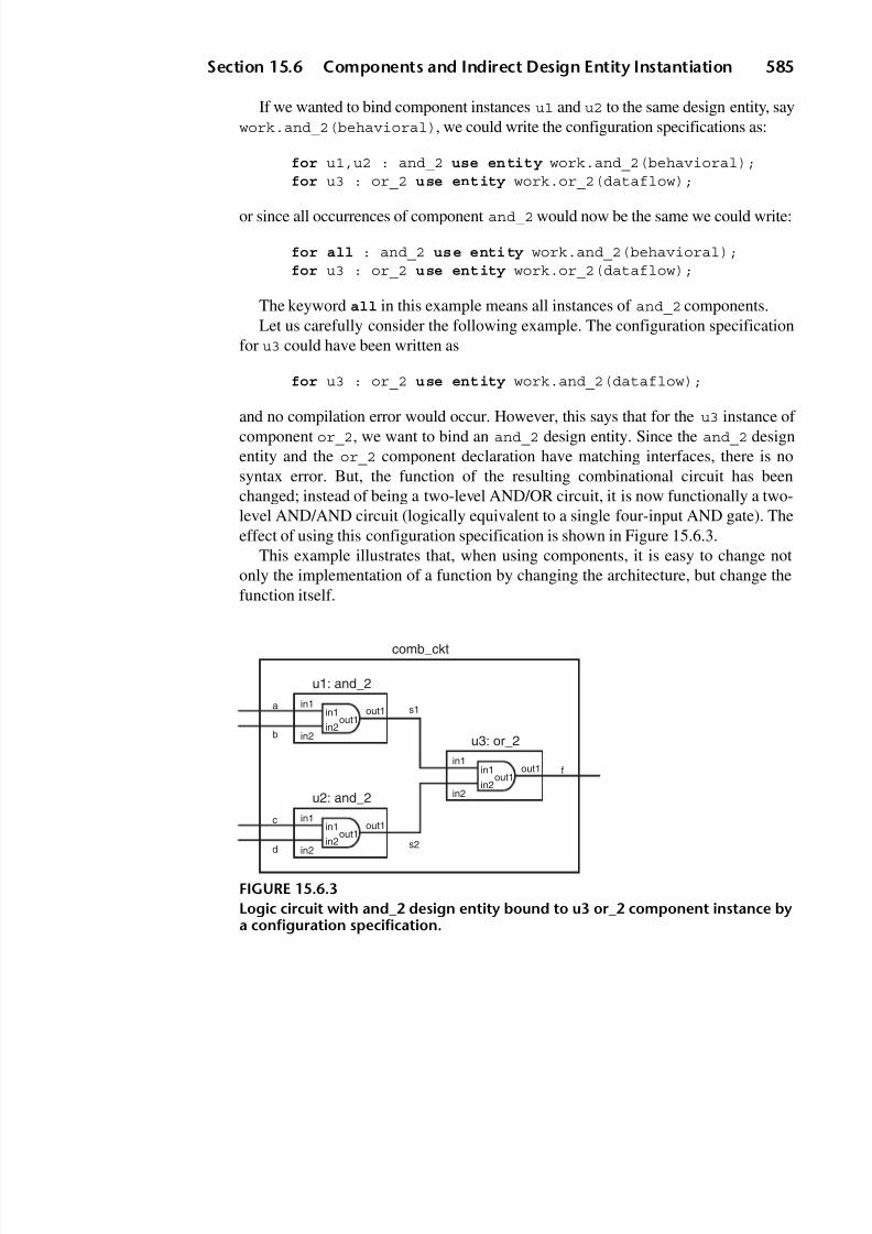
8/9/2019 VHDL for Engineers - Kenneth L. Short.pdf
http://slidepdf.com/reader/full/vhdl-for-engineers-kenneth-l-shortpdf 618/719
Section 15.6 Components and Indirect Design Entity Instantiation 585
If we wanted to bind component instances u1 and u2 to the same design entity, saywork.and_2(behavioral), we could write the configuration specifications as:
for u1,u2 : and_2 use entity work.and_2(behavioral);for u3 : or_2 use entity work.or_2(dataflow);
or since all occurrences of component and_2 would now be the same we could write:
for all : and_2 use entity work.and_2(behavioral);for u3 : or_2 use entity work.or_2(dataflow);
The keyword all in this example means all instances of and_2 components.Let us carefully consider the following example. The configuration specification
for u3 could have been written as
for u3 : or_2 use entity work.and_2(dataflow);
and no compilation error would occur. However, this says that for the u3 instance of component or_2, we want to bind an and_2 design entity. Since the and_2 designentity and the or_2 component declaration have matching interfaces, there is nosyntax error. But, the function of the resulting combinational circuit has beenchanged; instead of being a two-level AND/OR circuit, it is now functionally a two-level AND/AND circuit (logically equivalent to a single four-input AND gate). Theeffect of using this configuration specification is shown in Figure 15.6.3.
This example illustrates that, when using components, it is easy to change notonly the implementation of a function by changing the architecture, but change thefunction itself.
FIGURE 15.6.3
Logic circuit with and_2 design entity bound to u3 or_2 component instance bya configuration specification.
in1
in2
in1
in2
in1
in2
out1
in1
in2
in1
in2
s1
s2
u1: and_2
comb_ckt
u3: or_2
in1
in2out1
a
b
out1
out1
out1
out1
u2: and_2
c
d
f

8/9/2019 VHDL for Engineers - Kenneth L. Short.pdf
http://slidepdf.com/reader/full/vhdl-for-engineers-kenneth-l-shortpdf 619/719
586 Chapter 15 Modular Design and Hierarchy
Port Maps inConfigurationSpecifications
A port map can be included in a configuration specification to configure a designentity to be compatible with a component declaration even though their interfaces donot exactly match. For example, assume that we did not have a design entity or_2 tobind to the component or_2, but we did have a three-input OR design entity in thelibrary parts. Assume that the entity declaration for the three-input OR or_3 is:
entity or_3 is
port( inp1, inp2, inp3 : in std_logic;outp1 : out std_logic );
end or_3;
We can change the configuration specification for u3 in Listing 15.6.2 to:
for u3 : or_2 use entity parts.or_3(dataflow)port map (inp1 => in1, inp2 => in2, inp3 => '0',
outp1 => f);
This configuration specification includes a port map that maps the ports of thedesign entity or_3 to the ports of the or_2 component. The third input of the or_3entity is mapped to the expression '0' (Figure 15.6.4).
A library clause that makes the library parts visible is required. However, a useclause is not required, since that is taken care of in the configuration specification.
The ability to use a port map in a configuration specification to bind a componentinstance to a design entity whose interface does not exactly match is very useful. Itallows us to maximize the reuse of some design entities without modifying theiroriginal code.
FIGURE 15.6.4
Logic circuit with or_3 design entity bound to u3 or_2 component instance by aconfiguration specification containing a port map.
entity or_3
in1
in2
in1
in2
in1
in2
out1
inp1inp2inp3
in1
in2
in1in2
‘0’outp1
s1
s2
u1: and_2
comb_ckt
u3: or_2
a
b
out1
out1
out1
out1
u2: and_2
c
d
f

8/9/2019 VHDL for Engineers - Kenneth L. Short.pdf
http://slidepdf.com/reader/full/vhdl-for-engineers-kenneth-l-shortpdf 620/719
Section 15.7 Configuration Declarations 587
1 5. 7 C ON FI GU RA TI ON D EC LA RA TI ON S
Using configuration specifications, as in the previous section, is advantageous whenwe don’t intend to change our component-instance/design-entity bindings. Greater
flexibility in specifying bindings can be achieved using a configuration declaration.A configuration declaration is a design unit that allows bindings of architecture
bodies to entity declarations, as well as bindings of components to design entities, to bespecified. Since a configuration declaration is a separate design unit, these bindings arespecified outside of the architecture body.
ConfigurationDeclaration Syntax
The simplified syntax for a configuration declaration is given in Figure 15.7.1.Configuration declarations can be quite complex. We will consider some straight-forward examples.
Specifyingan Architectureto Be Bound
The simplest use of a configuration declaration is to specify the binding of an archi-tecture to a design entity when the architecture is not structural (does not contain anycomponents). Suppose that we had a second architecture for comb_ckt that was adataflow architecture named dataflow. We now have two different architectures fordesign entity comb_ckt. If we simulated comb_ckt, by default, the most recentlycompiled architecture would be used.
Suppose that we wanted to simulate comb_ckt using the dataflow architectureand it was not the most recently compiled. We could create a configuration decla-ration to specify that architecture dataflow be used. This configuration declarationis given in Listing 15.7.1.
The first line of the configuration declaration in Listing 15.7.1 consists of keywordconfiguration, followed by the name config1, which we have chosen to givethis configuration. Following keyword of is the name of the entity being configured.
The second line specifies the name of the architecture, dataflow, that is boundto the design entity.
configuration_declaration ::=
configuration identifier of entity _name is
for architecture _name
{ for component_specification binding_indication ;end for ; }
end for ;
end [ configuration ] [ configuration _simple_name ] ;
FIGURE 15.7.1
Simplified syntax for a configuration declaration.
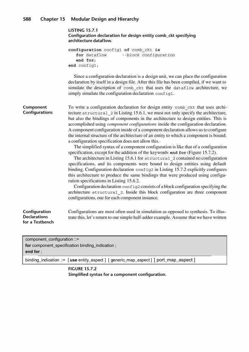
8/9/2019 VHDL for Engineers - Kenneth L. Short.pdf
http://slidepdf.com/reader/full/vhdl-for-engineers-kenneth-l-shortpdf 621/719
588 Chapter 15 Modular Design and Hierarchy
LISTING 15.7.1Configuration declaration for design entity comb_ckt specifyingarchitecture dataflow.
configuration config1 of comb_ckt is
for dataflow --block configuration
end for;end config1;
Since a configuration declaration is a design unit, we can place the configurationdeclaration by itself in a design file. After this file has been compiled, if we want tosimulate the description of comb_ckt that uses the dataflow architecture, wesimply simulate the configuration declaration config1.
ComponentConfigurations
To write a configuration declaration for design entity comb_ckt that uses archi-tecture structural_2 in Listing 15.6.1, we must not only specify the architecture,
but also the bindings of components in the architecture to design entities. This isaccomplished using component configurations inside the configuration declaration.A component configuration inside of a component declaration allows us to configurethe internal structure of the architecture of an entity to which a component is bound;a configuration specification does not allow this.
The simplified syntax of a component configuration is like that of a configurationspecification, except for the addition of the keywords end for (Figure 15.7.2).
The architecture in Listing 15.6.1 for structural_2 contained no configurationspecifications, and its components were bound to design entities using defaultbinding. Configuration declaration config2 in Listing 15.7.2 explicitly configuresthis architecture to produce the same bindings that were produced using configu-ration specifications in Listing 15.6.2.
Configuration declaration config2 consists of a block configuration specifying thearchitecture structural_2. Inside this block configuration are three componentconfigurations, one for each component instance.
ConfigurationDeclarationsfor a Testbench
Configurations are most often used in simulation as opposed to synthesis. To illus-trate this, let’s return to our simple half-adder example. Assume that we have written
component_configuration ::=
for component_specification binding_indication ;
end for ;
binding_indication ::= [ use entity_aspect ] [ generic_map_aspect ] [ port_map_aspect ]
FIGURE 15.7.2
Simplified syntax for a component configuration.

8/9/2019 VHDL for Engineers - Kenneth L. Short.pdf
http://slidepdf.com/reader/full/vhdl-for-engineers-kenneth-l-shortpdf 622/719
Section 15.7 Configuration Declarations 589
LISTING 15.7.2Configuration declaration for structural architecture for comb_ckt.
configuration config2 of comb_ckt is
for structural_2 -- block configurationfor u1 : and_2 -- component configuration
use entity work.and_2(dataflow);end for;for u2 : and_2 -- component configuration
use entity work.and_2(behavioral);end for;for u3 : or_2 -- component configuration
use entity work.or_2(dataflow);end for;
end for;end config2;
a dataflow description of a half-adder, and also have written a testbench namedtestbench that is suitable for performing either a functional, post-synthesis, ortiming simulation. The architecture for the entity testbench is named behavior. Inits declarative part, we declare a component named half_adder. In the architecturebody’s statement part, component half_adder is instantiated having the label UUT.
Configurationfor FunctionalSimulation
When we compile the half-adder description, we get the design entity half_
adder(dataflow). We can write a configuration declaration named functional_sim for design entity testbench that binds the instance UUT of componenthalf_adder to design entity half_adder(dataflow) (Listing 15.7.3). We can
then simulate configuration declaration functional_sim to perform a functionalsimulation. Note that, when using a configuration declaration to simulate the UUT, weare not actually simulating the testbench, but rather the configuration declaration forthe testbench.
Configurationfor Post-SynthesisSimulation
When we synthesize the half-adder description, we get a gate-level model of thedesign entity. If we examine the text of this model, we can see the name that thesynthesizer has given the resulting gate-level architecture. Assume that this architecture
LISTING 15.7.3Configuration declaration for a functional simulation of a half adder.
configuration functional_sim of testbench is
for behaviorfor UUT : half_adder
use entity work.half_adder(dataflow);end for;
end for;end functional_sim

8/9/2019 VHDL for Engineers - Kenneth L. Short.pdf
http://slidepdf.com/reader/full/vhdl-for-engineers-kenneth-l-shortpdf 623/719
590 Chapter 15 Modular Design and Hierarchy
LISTING 15.7.4Configuration declaration for a post-synthesis simulation of a half adder.
configuration postsyn_sim of testbench is
for behaviorfor UUT : half_adder
use entity work.half_adder(beh);end for;
end for;end postsyn_sim
is named beh. We can then write a configuration declaration named postsyn_sim fordesign entity testbench that binds instance UUT of component half_adder to thegate-level design entity half_adder(beh) (Listing 15.7.4). We can then simulateconfiguration declaration postsyn_sim to perform a post-synthesis simulation.
Configuration forTiming Simulation
When we place and route the half-adder’s EDIF netlist that resulted from thesynthesis, we get a timing-model design entity for the half adder placed and routedto the target PLD. If we examine the text of this model, we can see the name that theplace-and-route tool has given the resulting timing model architecture. Assume thatthis architecture is named structure. We can write a configuration declarationnamed timing_sim for design entity testbench that binds instance UUT of component half_adder to timing model design entity half_adder(structure)
(Listing 15.7.5). We can then simulate configuration declaration timing_sim toperform a timing simulation.
In summary, with three different half-adder architectures—a functional model, a
gate-level model, and a timing model—we can use one of the three different config-urations to bind component UUT in the testbench to the desired half-adder designentity and architecture.
Using this approach, the configuration declaration becomes the top level in thesimulation. Depending on which simulation we wish to perform, we simply simulatethe appropriate configuration declaration. The instantiation statement for the UUT inthe testbench does not need to be modified, saving us time.
LISTING 15.7.5Configuration declaration for a timing simulation of a half adder.
configuration timing_sim of testbench is
for behaviorfor UUT : half_adder
use entity work.half_adder(structure);end for;
end for;end timing_sim

8/9/2019 VHDL for Engineers - Kenneth L. Short.pdf
http://slidepdf.com/reader/full/vhdl-for-engineers-kenneth-l-shortpdf 624/719
Section 15.7 Configuration Declarations 591
LISTING 15.7.6Multilevel structural architecture for a half adder.
use work.gates.all;architecture structural of half_adder is -- Architecture body for half adder
component xor_2port (in1, in2 : in std_logic;
out1: out std_logic);end component;
begin
u1: component xor_2 port map (in1 => a, in2 => b, out1 => sum);u2: component and_2 port map (i1 => a, i2 => b, o1 => carry_out);
end structural;
ConfiguringMultilevelHierarchies
In the previous half-adder example, the original description of half_adder wasbound to a behavioral architecture. As a result, the testbench had a single level of partitioning and the UUT was instantiated at that level. If, instead, the half adderwere bound to a structural architecture, there would be an additional level of parti-tioning, resulting in a multilevel hierarchy.
For example, assume that components and_2, or_2, and invert are declared ina package named gates. A structural architecture for the half adder is given inListing 15.7.6.
This architecture instantiates two components. Component xor_2 is declared in thedeclarative part of the architecture. Component and_2 is declared in package gates.
Assume that the only behavioral design entities we have are named and_2x,
or_2x, and invert2x, and they are compiled to library work. Component and_2can be bound to design entity and_2x, but this cannot be done by default, becausethe component and entity names are different.
For the XOR function, assume we have the structural description in Listing 15.7.7.
LISTING 15.7.7Structural description of an XOR function.
library ieee;use ieee.std_logic_1164.all;
entity xor_2x is
port(in1, in2 : in std_logic;out1 : out std_logic);
end xor_2x;(Cont.)

8/9/2019 VHDL for Engineers - Kenneth L. Short.pdf
http://slidepdf.com/reader/full/vhdl-for-engineers-kenneth-l-shortpdf 625/719
592 Chapter 15 Modular Design and Hierarchy
LISTING 15.7.7 (Cont.)
use work.gates.all;architecture structural of xor_2x is
signal s1, s2, s3, s4 : std_logic;begin
u1: component invert port map (i => in2, o => s1);u2: component invert port map (i => in1, o => s2);u3: component and_2 port map (i1 => in1, i2 => s1, o1 => s3);u4: component and_2 port map (i1 => s2, i2 => in2, o1 => s4);u5: component or_2 port map (i1 => s3, i2 => s4, o1 => out1);
end structural;
The components in this description can each be explicitly bound to one of the
existing behavioral design entities, and_2x, or_2x, and invert2x, in library work.A more complex version of the syntax for a configuration declaration is given inFigure 15.7.3.
This version of the syntax for a configuration declaration has a recursive form withrespect to the block configuration.
The configuration declaration in Listing 15.7.8 uses a single configuration decla-ration to configure the multilevel hierarchy of half_adder to use the behavioraldesign entities and_2x, or_2x, and invert2x.
SeparateConfiguration
Declarationsfor MultilevelHierarchies
Rather than use the recursive capability of a single configuration declaration, asimpler approach to configuring a multilevel architecture is to use separate configu-
ration declarations. This approach makes the overall configuration of a multilevelhierarchy easier to write and comprehend.
configuration_declaration ::=
configuration identifier of entity _name is
block_configuration
end [ configuration ] [ configuration _simple_name ] ;
block_configuration ::=
for architecture _name{ for component_specification [ binding_indication ; ]
[ block_configuration ]
end for ;}
end for ;
FIGURE 15.7.3
Syntax for configuration declaration.

8/9/2019 VHDL for Engineers - Kenneth L. Short.pdf
http://slidepdf.com/reader/full/vhdl-for-engineers-kenneth-l-shortpdf 626/719
Section 15.7 Configuration Declarations 593
LISTING 15.7.8Configuration for multilevel structural half-adder architecture.
configuration functional_sim2 of testbench is
for behavior -- architecture of testbenchfor UUT : half_adder use entity work.half_adder(structural);
for structural -- architecture of half adder for u2: and_2 use entity work.and_2x(dataflow);end for;for u1 : xor_2 use entity work.xor_2x(structural);
for structural -- architecture of xor_2x for u1, u2 : invert use entity work.invertx(dataflow);end for;for u3, u4 : and_2 use entity work.and_2x(dataflow);end for;for u5 : or_2 use entity work.or_2x(dataflow);end for;
end for;end for;end for;
end for;end for;
end functional_sim2
We can write separate configuration declarations for each structural architecture.For example, a configuration for entity xor_2x is given in Listing 15.7.9.
We can then write a configuration declaration for half_adder that takesadvantage of the existing configuration xor_2x_config for xor_2x. This is possiblebecause a binding indication can use a configuration. A configuration declaration forhalf_adder that uses the configuration declaration for xor_2x to specify thebinding of component u1 of the half_adder is given in Listing 15.7.10.
LISTING 15.7.9Configuration declaration for entity xor_2x.
--Entity-Architecture Pair Configurationconfiguration xor_2x_config of xor_2x is
for structural -- architecture of xor_2x
for u1, u2 : invert use entity work.invertx(dataflow);end for;for u3, u4 : and_2 use entity work.and_2x(dataflow);end for;for u5 : or_2 use entity work.or_2x(dataflow);end for;
end for;end xor_2x_config;

8/9/2019 VHDL for Engineers - Kenneth L. Short.pdf
http://slidepdf.com/reader/full/vhdl-for-engineers-kenneth-l-shortpdf 627/719
594 Chapter 15 Modular Design and Hierarchy
LISTING 15.7.10Configuration declaration for half_adder that uses an existing configuration declaration for xor_2x.
configuration functional_sim3 of testbench is
for behavior -- architecture of testbenchfor UUT : half_adder use entity work.half_adder(structural);
for structural -- architecture of half adder for u2: and_2 use entity work.and_2x(dataflow);end for;for u1 : xor_2 use configuration work.xor_2x_config;end for;
end for;end for;
end for;end functional_sim3
Using separate configurations in this fashion makes the overall configuration of a
multilevel design easier to understand.
15 .8 C OMP ON EN T C ON N EC T ION S
One of the purposes of a component instantiation statement is to specify themappings between the formal signals of an instance of a component and the actualsignals of the encompassing architecture. In this section we consider the intercon-nection of components in greater detail. While the discussion is in terms of component instantiation statements that use direct design entity instantiation, the
same considerations apply to design entities that are indirectly instantiated viacomponents.
Component PortConnections
Each port of a design entity is a formal port . For example, consider the entity decla-ration for a three-input AND function:
entity and_3 is
port (i1, i2, i3 : in std_logic;o1: out std_logic);
end and_3;
The formal ports of entity and_3 are: i1, i2, i3, and o1.The following entity declaration for an inverter
entity invert is
port (i: in std_logic; o: out std_logic);end invert;
has two formal ports i and o.

8/9/2019 VHDL for Engineers - Kenneth L. Short.pdf
http://slidepdf.com/reader/full/vhdl-for-engineers-kenneth-l-shortpdf 628/719
Section 15.8 Component Connections 595
Port Map Actuals The port map for a component instantiation describes how a design entity isconnected, as a component, in a larger structure in which it is used. In a componentinstantiation, each formal port of the component is associated with an actual of theenclosing architecture. An actual can be an expression, a signal, or a port.
Expression Actual An expression is used to provide a port with a constant driving value. Accordingly,an expression can only be an actual for a formal port of mode in.
Signal Actual A local signal, declared in the enclosing design entity’s architecture body, has nomode and can, therefore, be used as an actual for a formal port of any mode. This isillustrated in Figure 15.8.1. In this figure, component u1’s output port is connected toa signal. In u1’s port map, its output port is a formal that is associated with an actualthat is this signal. In u2’s port map, its input port is a formal associated with an actualthat is the same signal.
Enclosing DesignEntity Portsas Actuals
A port is also a signal, but a port has a mode. A formal port of the enclosing designentity can be associated as the actual for a formal port of a component.
In Figure 15.8.1, component u1’s input port is directly connected to the input portof the enclosing design entity, without the need for a local signal. This is representedby the dotted line in the figure. In u1’s port map, its input port is a formal that isassociated with an actual that is the formal input port of the enclosing design entity.
Component u2’s output port is directly connected to the output port of theenclosing design entity. In u2’s port map, its output port is a formal that is associatedwith an actual that is the formal output port of the enclosing design entity.
When a formal port is associated with an actual that is itself a port (of the
enclosing design entity), the restrictions in Table 15.8.1 apply.
FIGURE 15.8.1
Graphical representation of association of component formals with actuals.
Top-level entity
signal
f f faa
U1 U2
in in inout out out
port f formala actual
f a
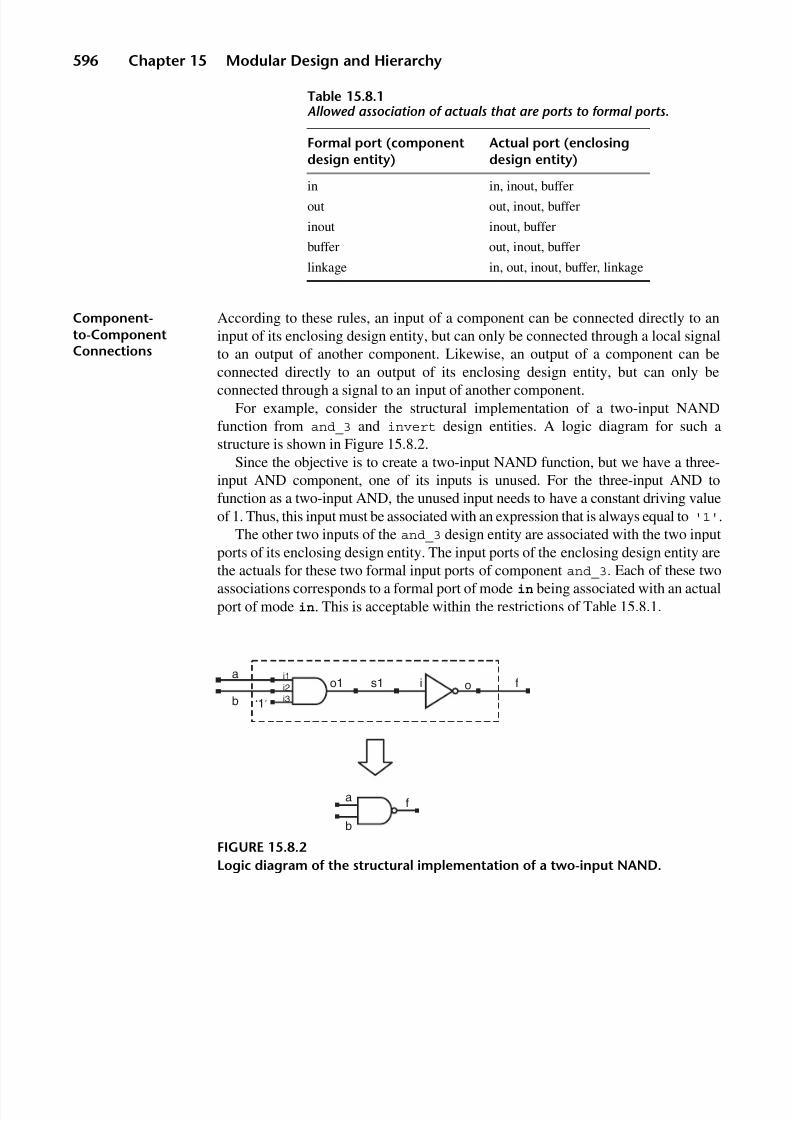
8/9/2019 VHDL for Engineers - Kenneth L. Short.pdf
http://slidepdf.com/reader/full/vhdl-for-engineers-kenneth-l-shortpdf 629/719
596 Chapter 15 Modular Design and Hierarchy
Component-to-ComponentConnections
According to these rules, an input of a component can be connected directly to aninput of its enclosing design entity, but can only be connected through a local signalto an output of another component. Likewise, an output of a component can be
connected directly to an output of its enclosing design entity, but can only beconnected through a signal to an input of another component.For example, consider the structural implementation of a two-input NAND
function from and_3 and invert design entities. A logic diagram for such astructure is shown in Figure 15.8.2.
Since the objective is to create a two-input NAND function, but we have a three-input AND component, one of its inputs is unused. For the three-input AND tofunction as a two-input AND, the unused input needs to have a constant driving valueof 1. Thus, this input must be associated with an expression that is always equal to '1'.
The other two inputs of the and_3 design entity are associated with the two inputports of its enclosing design entity. The input ports of the enclosing design entity are
the actuals for these two formal input ports of component and_3. Each of these twoassociations corresponds to a formal port of mode in being associated with an actualport of mode in. This is acceptable within the restrictions of Table 15.8.1.
Table 15.8.1Allowed association of actuals that are ports to formal ports.
Formal port (componentdesign entity)
Actual port (enclosingdesign entity)
in in, inout, bufferout out, inout, buffer
inout inout, buffer
buffer out, inout, buffer
linkage in, out, inout, buffer, linkage
FIGURE 15.8.2
Logic diagram of the structural implementation of a two-input NAND.
a
b
i1
i2
i3‘1’
o1 s1 o fi
a
b
f

8/9/2019 VHDL for Engineers - Kenneth L. Short.pdf
http://slidepdf.com/reader/full/vhdl-for-engineers-kenneth-l-shortpdf 630/719
Section 15.8 Component Connections 597
The output of the and_3 component needs to be connected to the input of theinvert component. A direct connection would (from the viewpoint of the and_3
component) correspond to a formal port of mode out being associated with an actualport of mode in. Since this is not allowed (Table 15.8.1), the output of and_3 mustbe connected to a signal. This requires the declaration of a local signal, which we
call s1. Accordingly, the component instantiation statement for the and_3 is:
u1: entity and_3port map (i1 => a, i2 => b, i3 => '1',
o1 => s1);
In writing the component instantiation statement for the inverter, its formal portof mode in must be connected to a signal, since it cannot be directly connected to anactual port of mode out (Table 15.8.1). Accordingly, it is connected to signal s1.The actual for the inverter’s formal port of mode out is the output port of theenclosing design entity. This results in the following instantiation statement:
u2: entity invert port map (i => s1, o => f);
The complete design file is given in Listing 15.8.1.
LISTING 15.8.1Design file for structural implementation of a two-input NAND function.
------------------------- 3 input AND gate component --------------------------library ieee;use ieee.std_logic_1164.all;
entity and_3 is-- Entity declaration for 2 input and port (i1, i2, i3 : in std_logic;
o1: out std_logic);end and_3;
architecture dataflow of and_3 is-- Architecture body for 3 input and begin
o1 <= i1 and i2 and i3;end dataflow;
------------------- Inverter entity library ieee;use ieee.std_logic_1164.all;
entity invert is
port (i: in std_logic; o: out std_logic);end invert;
(Cont.)

8/9/2019 VHDL for Engineers - Kenneth L. Short.pdf
http://slidepdf.com/reader/full/vhdl-for-engineers-kenneth-l-shortpdf 631/719
598 Chapter 15 Modular Design and Hierarchy
LISTING 15.8.2 (Cont.)
architecture dataflow of invert is
begin
o <= not i;end dataflow;
------------------------- 2-input NAND structure ---------------------------library ieee;use ieee.std_logic_1164.all;
entity nand_2 is-- Entity declaration for half adder port (a, b : in std_logic;
f: out std_logic);end nand_2;
architecture structure of nand_2 is-- Architecture body for half adder
signal s1 : std_logic;
begin
u1: entity and_3 port map (i1 => a, i2 => b, i3 => '1', o1 => s1);u2: entity invert port map (i => s1, o => f);
end structure;
Open Keyword If a formal port is associated with an expression, signal, or actual port, then theformal port is said to be connected. If a formal port is instead associated with the
keyword open, then the formal is said to be unconnected. A port of mode in may beunconnected or unassociated only if its declaration includes a default expression. Aport of any mode other than in may be unconnected or unassociated, as long as itstype is not an unconstrained array type.
If a port is simply omitted from the association list, it is considered open. If anassociation element is omitted from an association list for this purpose, all subse-quent associations in the list must be named associations. Using keyword open ispreferable to simply omitting a port, because keyword open makes it clear that theport was intentionally left open.
1 5. 9 P AR AM ET ER IZ ED D ES IG N EN TI TI ES
Design entities are more widely reusable if they are parameterized. Parametersallow a design entity to be described generically so that, for each use of the designentity, its structure and/or behavior is altered by the choice of parameter values. InVHDL these parameters are called generics. Generics were introduced in the section

8/9/2019 VHDL for Engineers - Kenneth L. Short.pdf
http://slidepdf.com/reader/full/vhdl-for-engineers-kenneth-l-shortpdf 632/719
Section 15.9 Parameterized Design Entities 599
“Timing Models Using VITAL and SDF” on page 288, where they were used tospecify delays in timing models.
Default generic values for a design entity can be specified inside its entity decla-
ration. If not overridden, these are the values of the generics. Recall that these valuescan be overridden from outside of the design entity in either the component instanti-ation statement or a configuration declaration.
The expanded syntax for an entity declaration that includes a formal genericclause is repeated in Figure 15.9.1. When generics are used, the generic clauseprecedes the port clause.
Once declared, a generic can be used in the entity declaration itself and in allarchitectures associated with the entity.
Counter UsingGenerics
In parameterizing design descriptions, generics are often used to specify the width of data objects. For example, consider the 12-bit counter from Listing 9.4.4. A parame-terized version of the counter is given in Listing 15.9.1. A single generic n is used tospecify the size (number of bits) of the counter.
LISTING 15.9.1Parameterized binary counter.
library ieee;use ieee.std_logic_1164.all;use ieee.numeric_std.all;
entity binary_cntr is
generic (n : positive := 12); -- counter size (bits)port (clk, cnten, up, rst_bar: in std_logic;
q: out std_logic_vector (n - 1 downto 0));end binary_cntr;
architecture behav_param of binary_cntr is
begin
(Cont.)
entity_declaration ::=
entity identifier is
[ generic ( generic _interface_list ) ; ]
[ port ( port _interface_list ) ; ]
end [ entity ] [ entity _simple_name ] ;
generic _interface_list ::=
[ constant ] identifier_list : [ in ] subtype_indication [ := static _expression ]
{[ constant ] identifier_list : [ in ] subtype_indication [ := static _expression ]}
FIGURE 15.9.1
Expanded syntax for an entity declaration that includes a formal generic clause.
8/9/2019 VHDL for Engineers - Kenneth L. Short.pdf
http://slidepdf.com/reader/full/vhdl-for-engineers-kenneth-l-shortpdf 633/719
600 Chapter 15 Modular Design and Hierarchy
LISTING 15.9.1 (Cont.)
cntr: process (clk)variable count_v : unsigned(n - 1 downto 0);
begin
if rising_edge(clk) then
if rst_bar = '0' then
count_v := (others => '0');elsif cnten = '1' then
case up is
when '1' => count_v := count_v + 1; when others => count_v := count_v - 1;
end case;else
null;end if;q <= std_logic_vector(count_v);
end if;end process;
end behav_param;
The first statement in the entity declaration is a formal generic clause:
generic (n : positive := 12);
The generic clause precedes the port clause. This generic clause lists a singlegeneric named n of type positive that has a default value of 12. Specification of adefault value is not required. The generic clause could have been written as:
generic (n : positive);
The port clause in the entity declaration uses generic n to specify the width of thecounter’s output q. In the architecture body, generic n is used to specify the width of the unsigned variable count_v. As a result, the number of bits in the counter can beset to any positive value.
Generic MapAspect
When a design entity using generics is instantiated in a structural description, theinstantiation statement can include a generic map aspect that assigns values to the
generics. The syntax for a generic map aspect is given in Figure 15.9.2.When the design entity binary_cntr is instantiated, if no other value is specified
for the generic in the instantiation statement, a 12-bit counter is created by default:
u3: entity binary_cntr(behav_param)port map (clk => clk, cnten => cnten_sig,
up => up_sig, rst_bar => rst_bar,q => count_sig);

8/9/2019 VHDL for Engineers - Kenneth L. Short.pdf
http://slidepdf.com/reader/full/vhdl-for-engineers-kenneth-l-shortpdf 634/719
Section 15.9 Parameterized Design Entities 601
Alternatively, we can give the counter any desired width by including a genericmap aspect in the instantiation statement and specifying the desired value for n:
u3: entity binary_cntr(behav_param)generic map (n => 10)port map (clk => clk,cnten => cnten_sig,
up => up_sig,rst_bar => rst_bar,q => count_sig);
The counter in this instantiation is a 10-bit counter, since the value of 10 assignedto n in the generic map overrides the default value of 12 in the counter’s entity decla-ration. Note that there is no semicolon between the generic map aspect and port mapaspect in a component instantiation.
Local GenericClause inComponentDeclaration
If we are using generics, but are not using direct entity instantiation, as in theprevious two instantiation statements, there must be a component declaration in thedeclarative part of the architecture that instantiates the component and this decla-ration must contain a local generic clause. For example:
component binary_cntrgeneric (n : positive);port (clk, cnten, up, rst_bar: in std_logic;q: out std_logic_vector (n - 1 downto 0));
end component;
PLD Vendorand Third-PartyParameterizedModules
PLD vendors and their third-party IP partners provide libraries containing parame-terized functional modules that we can use as components in our designs. Thisspeeds up the design process. These modules’ functionalities range from gates tomultiply accumulate subsystems. To provide scalability and adaptability, modules
are configured using generics.These module libraries fall into two categories: those containing architecture
dependent modules and those containing architecture independent modules. Archi-tecture dependent modules are optimized for the architecture of a particular PLDfamily. They are highly efficient in their use of the target PLD’s logic resources andprovide high performance. The drawback to using these modules is that they are notportable to other PLD families.
generic_map_aspect ::=
generic map ( generic _association_list )
association_list ::=
[ formal_part => ] actual_part { , [ formal_part => ] actual_part }
FIGURE 15.9.2
Syntax for a generic map aspect.
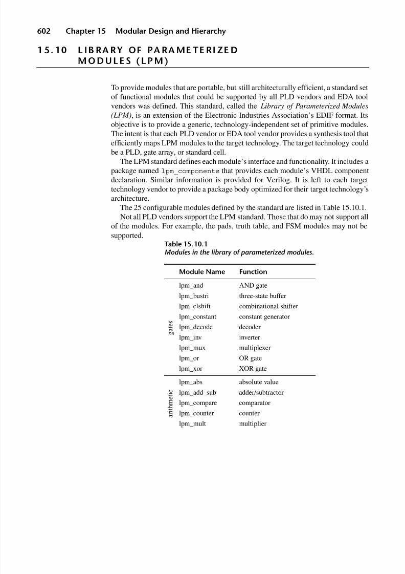
8/9/2019 VHDL for Engineers - Kenneth L. Short.pdf
http://slidepdf.com/reader/full/vhdl-for-engineers-kenneth-l-shortpdf 635/719
602 Chapter 15 Modular Design and Hierarchy
1 5. 10 L IB RA RY OF PA RA ME TE RI ZE D M O D U L E S ( L P M )
To provide modules that are portable, but still architecturally efficient, a standard set
of functional modules that could be supported by all PLD vendors and EDA toolvendors was defined. This standard, called the Library of Parameterized Modules
(LPM), is an extension of the Electronic Industries Association’s EDIF format. Itsobjective is to provide a generic, technology-independent set of primitive modules.The intent is that each PLD vendor or EDA tool vendor provides a synthesis tool thatefficiently maps LPM modules to the target technology. The target technology couldbe a PLD, gate array, or standard cell.
The LPM standard defines each module’s interface and functionality. It includes apackage named lpm_components that provides each module’s VHDL componentdeclaration. Similar information is provided for Verilog. It is left to each targettechnology vendor to provide a package body optimized for their target technology’sarchitecture.
The 25 configurable modules defined by the standard are listed in Table 15.10.1.Not all PLD vendors support the LPM standard. Those that do may not support all
of the modules. For example, the pads, truth table, and FSM modules may not besupported.
Table 15.10.1Modules in the library of parameterized modules.
Module Name Function
g a t e s
lpm_and AND gate
lpm_bustri three-state buffer
lpm_clshift combinational shifter
lpm_constant constant generator
lpm_decode decoder
lpm_inv inverter
lpm_mux multiplexer
lpm_or OR gate
lpm_xor XOR gate
a r i t h m e t i c
lpm_abs absolute value
lpm_add_sub adder/subtractor
lpm_compare comparator
lpm_counter counter
lpm_mult multiplier

8/9/2019 VHDL for Engineers - Kenneth L. Short.pdf
http://slidepdf.com/reader/full/vhdl-for-engineers-kenneth-l-shortpdf 636/719
Section 15.10 Library of Parameterized Modules (LPM) 603
UsingParameterizedModules
As an example of the use of a LPM module, suppose that we need an 8-bit registerwith an asserted-high asynchronous clear. The lpm_ff module can be configured toprovide this functionality. Its declaration is given in Listing 15.10.1.
LISTING 15.10.1Component declaration for module lpm_ff.
component lpm_ff
generic(lpm_width : natural; -- must be greater than 0
lpm_avalue : string := "unused";lpm_svalue : string := "unused";lpm_pvalue : string := "unused";lpm_fftype: string := "dff";lpm_type: string := l_ff;lpm_hint : string := "unused");
port (data : in std_logic_vector(lpm_width-1 downto 0) := (others => '1');clock : in std_logic;enable : in std_logic := '1';sload : in std_logic := '0';
sclr : in std_logic := '0';sset : in std_logic := '0';aload : in std_logic := '0';aclr : in std_logic := '0';aset : in std_logic := '0';q : out std_logic_vector(lpm_width-1 downto 0));
end component
s t o r a g e
lpm_ff D or T flip-flop
lpm_latch latch
lpm_ram_dq RAM with separate I/O
lpm_ram_io RAM with common I/O
lpm_ROM ROM
lpm_shiftreg shift register
p a d s
lpm_bipad bidirectional I/O pad
lpm_inpad input pad
lpm_outpad output pad
o t h e r lpm_ttable truth table
lpm_fsm finite state machine
Module Name Function

8/9/2019 VHDL for Engineers - Kenneth L. Short.pdf
http://slidepdf.com/reader/full/vhdl-for-engineers-kenneth-l-shortpdf 637/719
604 Chapter 15 Modular Design and Hierarchy
LPM Generics Like most LPM modules, the lpm_ff module’s functionality is greater than its namemight imply. There are seven generics that configure the module. They can beassigned values in the generic map of a component instantiation statement.
The lpm_width generic determines the width of the register. If we wanted asingle flip-flop, we would set this value to 1. Otherwise, we set it to the desired
register width. The other six generics have default values specified in the componentdeclaration. If we wish to use the default value for a particular generic, then thatgeneric is simply omitted from the generic map.
The lpm_ff module can be configured as either a D or a T flip-flop based on thevalue of the lpm_fftype generic. The default value is "dff". Since that is thefunctionality we desire, we omit this generic from the generic map. If we wanted a Tflip-flop, we would assign lpm_fftype the value "tff" in the generic map. For ourexample, only the width needs to be assigned a value; defaults are appropriate for allthe other generics.
LPM Ports The declaration’s port clause specifies the inputs and outputs of the module. Inputdata is the data input and output q is the data output. Their widths are determinedby the value assigned to lpm_width. Input clock is for the system clock. Inputenable enables all synchronous operations. There are asynchronous set and clearinputs, aset and aclr, respectively. When aset is asserted, the register is set to1s or to the lpm_avalue specified in the generic map. There are also synchronousset and clear inputs, sset and sclr, respectively. When sset is asserted, theregister is set to 1s or to the lpm_svalue specified in the generic map. The aloadand sload inputs are only used when the module is configured as a T flip-flop.
A design entity that uses an instance of the lpm_ff module to create the desired8-bit register is given in Listing 15.10.2.
LISTING 15.10.2An 8-bit register implemented using an instance of the lpm_ff module.
library ieee;use ieee.std_logic_1164.all;library lpm;use lpm.lpm_components.all;
entity lpm_ff_reg is
port(clk : in std_logic; -- system clock rst : in std_logic; -- asserted-high resetdin : in std_logic_vector(7 downto 0); -- data inputq : out std_logic_vector(7 downto 0) -- data output);
end lpm_ff_reg;

8/9/2019 VHDL for Engineers - Kenneth L. Short.pdf
http://slidepdf.com/reader/full/vhdl-for-engineers-kenneth-l-shortpdf 638/719
Section 15.11 Generate Statement 605
architecture structural of lpm_ff_reg is
begin
reg0: lpm_ff generic map (lpm_width => 8) port map (clock => clk,data => din, aclr => rst, q => q);
end structural;
Context clause
library lpm;use lpm.lpm_components.all;
makes the module’s declaration visible.The component instantiation statement assigns a value to only the one generic it
needs to specify. It assigns signals to only the ports it needs to use. The synthesizershould synthesize only the LPM logic required for the functionality used.As we see from this simple example, using an LPM module requires an under-
standing of all the module’s inputs, outputs, and generics. This information is deter-mined from the standard or from documentation provided by the PLD vendor orthird-party IP vendor. Comments provided in the lpm_components package listingare usually not sufficient to provide all the needed information.
Many PLD vendors provide a wizard that allows us to answer questions about thefunctionality we require from a LPM module. The wizard then produces thecomponent instantiation code with the appropriate generic values. This simplifiesusing LPM modules.
15 .1 1 GE N ER AT E ST AT EMEN T
Many digital systems have a structure that consists of a number of repetitions of acomponent, where these repetitions form a regular pattern. Such systems can bedescribed by writing a separate component instantiation statement for each occur-rence of the component. However, since digital systems with this kind of regularstructure are so common, VHDL provides the generate statement to facilitate such
descriptions.A generate statement is a concurrent statement that allows us to specify the repli-
cation of concurrent statements. If a concurrent statement that is to be replicated is acomponent instantiation statement, then we have a concise way of describing therepeated instantiation of a component.
The syntax for a generate statement is given in Figure 15.11.1.

8/9/2019 VHDL for Engineers - Kenneth L. Short.pdf
http://slidepdf.com/reader/full/vhdl-for-engineers-kenneth-l-shortpdf 639/719
606 Chapter 15 Modular Design and Hierarchy
The generate_label is required to identify the generated structure. As a result of the generation_scheme chosen, there are two forms of generate statement. If the forscheme is chosen, we have an iterative generate statement. If the if condition scheme
is chosen, we have a conditional generate statement.Following keyword generate is an optional declarative part where we can
declare items. The kinds of items that can be declared here are the same as can bedeclared in the declarative part of an architecture body. Each item declared is local toeach replication of the concurrent statements. Following the optional declarative partare the concurrent statements to be generated.
Iterative GenerateStatement
When the for scheme is used, a discrete range must be specified. For each value in thisrange there is a replication of the declared items and the concurrent statements. Foreach replication the discrete range value is a constant called the generate parameter .
A very simple example of a digital system with a repetitive structure is an n-bitregister. Listing 9.1.2 provided a behavioral description of an 8-bit register withthree-state outputs. We can write a parameterized version of this register where itswidth is specified by a generic and its structure is created by replicating stages, eachof which consists of a D flip-flop component and a three-state buffer component.
Assume that we have compiled the D flip-flop description in Listing 8.4.1 and thethree-state buffer description in Listing 4.10.1 to the working library. We can write atop-level description, as shown in Listing 15.11.1, that uses an iterative generatestatement to describe the register.
LISTING 15.11.1Register with three-state buffer outputs described using a generate statement.
library ieee;use ieee.std_logic_1164.all;
entity reg_3sbuff_gen is
generic width : positive := 8);
generate_statement ::=
generate _label :
generation_scheme generate
[ { block_declarative_item }
begin ]
{ concurrent_statement }
end generate [ generate _label ] ;
generation_scheme ::= for generate _parameter_specification | if condition
FIGURE 15.11.1
Syntax for a generate statement.

8/9/2019 VHDL for Engineers - Kenneth L. Short.pdf
http://slidepdf.com/reader/full/vhdl-for-engineers-kenneth-l-shortpdf 640/719
Section 15.11 Generate Statement 607
port(d : in std_logic_vector(width - 1 downto 0);clk : in std_logic;oe_bar : in std_logic;q : out std_logic_vector(width - 1 downto 0));
end reg_3sbuff_gen;
architecture generated of reg_3sbuff_gen is
begin
stage: for i in (width - 1) downto 0 generate -- generate statementsignal s : std_logic ;begin
u0: entity work.d_ff_pe(behavioral) port map (d => d(i), clk => clk,q => s);
u1: entity work.three_state_buffer(dataflow) port map (d_in => s,en_bar => oe_bar, d_out => q(i));
end generate;end generated;
The entity declaration for the register declares the generic width and gives it adefault value of 8.
The architecture body consists of a single iterative generate statement with thelabel stage. The discrete range is specified as (width - 1) downto 0. If a configu-ration declaration is not used, width will have its default value of 8. If a configu-ration declaration is used, we can specify any desired width for the register.
Each stage of the register consists of a D flip-flop and a three-state buffer. A localsignal is needed in each stage to connect the output of the D flip-flop to the input of the three-state buffer. Accordingly, signal s is declared in the declaration part of thegenerate statement for this purpose.
In the statement part of the generate statement are two component instantiationstatements. One instantiates the D flip-flop, and the other instantiates the three-statebuffer. After the description is elaborated, there will be eight replications of theD flip-flop and eight replications of the three-state buffer. Each D flip-flop will beconnected to its associated three-state buffer by a replication of the local signal s.
A hierarchical view of the synthesized logic is given in Figure 15.11.2. Note theuse of the labels from the description in identifying the components in the block diagram. The replications of the local signal s are shown but not labeled.
InterconnectingAdjacent Instances
In the system shown in Figure 15.11.2, there are no connections from one D flip-flopand buffer instance to an adjacent instance. Such connections, by definition, cannotbe accomplished using signals local to an instance.
A simple example of a system that requires connections between adjacent componentinstances is a shift register. Consider the serial-in parallel-out 4-bit right-shift register inFigure 9.2.1. The component that must be replicated is a D flip-flop. We can use a
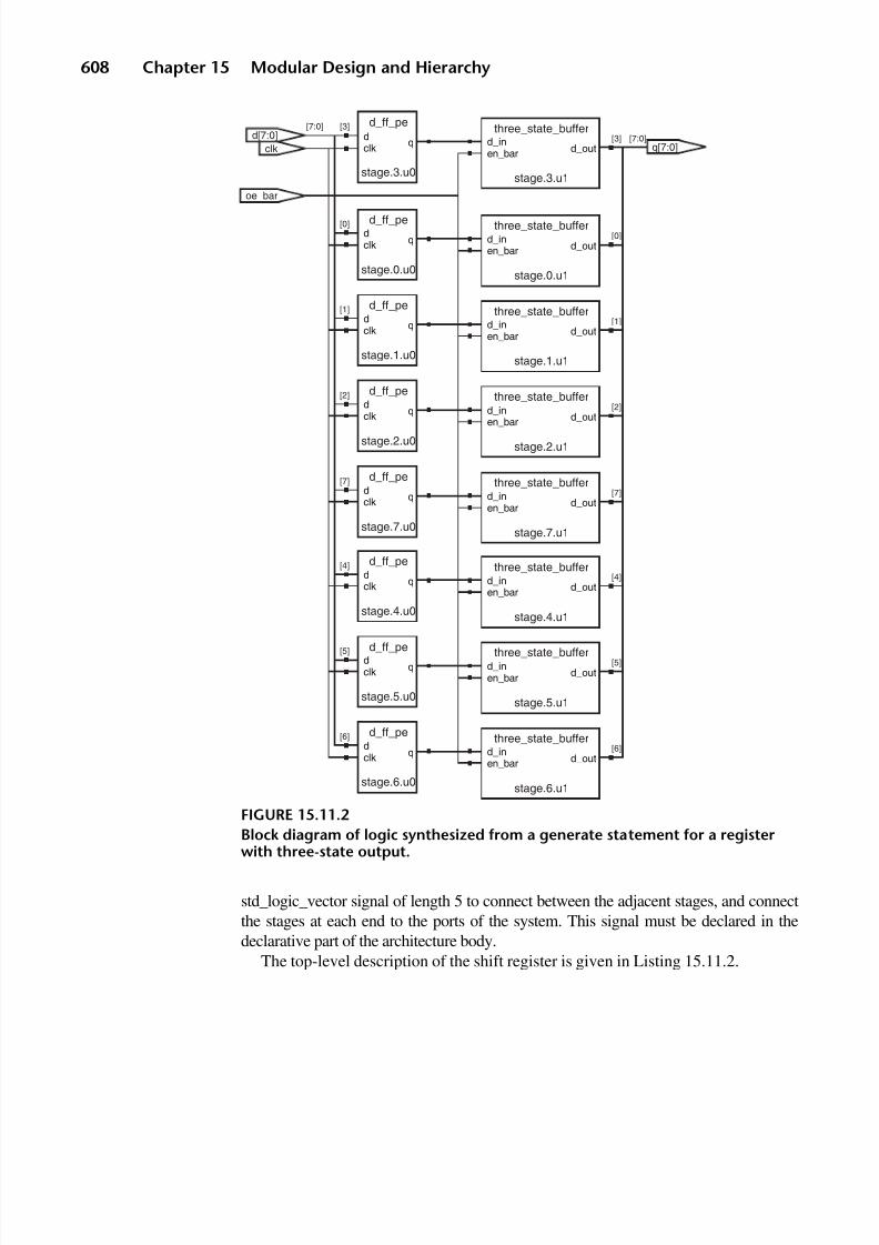
8/9/2019 VHDL for Engineers - Kenneth L. Short.pdf
http://slidepdf.com/reader/full/vhdl-for-engineers-kenneth-l-shortpdf 641/719
608 Chapter 15 Modular Design and Hierarchy
std_logic_vector signal of length 5 to connect between the adjacent stages, and connectthe stages at each end to the ports of the system. This signal must be declared in thedeclarative part of the architecture body.
The top-level description of the shift register is given in Listing 15.11.2.
FIGURE 15.11.2
Block diagram of logic synthesized from a generate statement for a registerwith three-state output.
d_ff_pe
stage.3.u0
d_ff_pe
stage.0.u0
d_ff_pe
stage.1.u0
d_ff_pe
stage.2.u0
d_ff_pe
stage.7.u0
d_ff_pe
stage.4.u0
d_ff_pe
stage.5.u0
d_ff_pe
stage.6.u0
three_state_buffer
stage.3.u1
three_state_buffer
stage.0.u1
three_state_buffer
stage.1.u1
three_state_buffer
stage.2.u1
three_state_buffer
stage.7.u1
three_state_buffer
stage.4.u1
three_state_buffer
stage.5.u1
three_state_buffer
stage.6.u1
q[7:0][7:0]
oe_bar
clk
d[7:0][7:0] [3]
dclk
q
[0]dclk
q
[1]dclk
q
[2]d
clk
q
[7]dclk
q
[4]dclk
q
[5]dclk
q
[6]dclk
q
d_inen_bar
[3]d_out
d_inen_bar
[0]
d_out
d_inen_bar
[1]d_out
d_in
en_bar
[2]
d_out
d_inen_bar
[7]d_out
d_inen_bar
[4]d_out
d_inen_bar
[5]
d_out
d_inen_bar
[6]
d_out
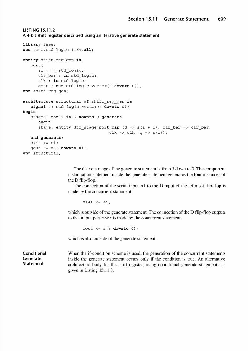
8/9/2019 VHDL for Engineers - Kenneth L. Short.pdf
http://slidepdf.com/reader/full/vhdl-for-engineers-kenneth-l-shortpdf 642/719
Section 15.11 Generate Statement 609
LISTING 15.11.2A 4-bit shift register described using an iterative generate statement.
library ieee;use ieee.std_logic_1164.all;
entity shift_reg_gen isport(
si : in std_logic;clr_bar : in std_logic;clk : in std_logic;qout : out std_logic_vector(3 downto 0));
end shift_reg_gen;
architecture structural of shift_reg_gen is
signal s: std_logic_vector(4 downto 0);begin
stages: for i in 3 downto 0 generatebegin
stage: entity dff_stage port map (d => s(i + 1), clr_bar => clr_bar,clk => clk, q => s(i));
end generate;s(4) <= si;qout <= s(3 downto 0);
end structural;
The discrete range of the generate statement is from 3 down to 0. The componentinstantiation statement inside the generate statement generates the four instances of the D flip-flop.
The connection of the serial input si to the D input of the leftmost flip-flop ismade by the concurrent statement
s(4) <= si;
which is outside of the generate statement. The connection of the D flip-flop outputsto the output port qout is made by the concurrent statement
qout <= s(3 downto 0);
which is also outside of the generate statement.
ConditionalGenerateStatement
When the if-condition scheme is used, the generation of the concurrent statementsinside the generate statement occurs only if the condition is true. An alternativearchitecture body for the shift register, using conditional generate statements, isgiven in Listing 15.11.3.

8/9/2019 VHDL for Engineers - Kenneth L. Short.pdf
http://slidepdf.com/reader/full/vhdl-for-engineers-kenneth-l-shortpdf 643/719
610 Chapter 15 Modular Design and Hierarchy
LISTING 15.11.3Alternative architecture body for the shift register.
architecture structural2 of shift_reg_gen is
signal s: std_logic_vector(3 downto 0);begin
stages: for i in 3 downto 0 generatebegin
lstage: if i = 3 generate
begin
stage: entity dff_stage port map (d => si,clr_bar => clr_bar, clk => clk, q => s(3));
end generate;
ostages: if i /= 3 generate
begin
stage: entity dff_stage port map (d => s(i + 1),
clr_bar => clr_bar, clk => clk, q => s(i));end generate;end generate;
qout <= s(3 downto 0);end structural2;
In the architecture body an iterative generate statement labeled stages sequencesthrough the values of its generate parameter. Nested inside this generate statement arethe two conditional generate statements. The first conditional statement, labeledlstage, has the conditioni = 3. When the generate parameter is equal to 3, this condi-
tional generate statement produces the instantiation of the leftmost stage of the shiftregister. The second conditional statement, labeled ostage, has the condition i/= 3.When the generate parameter is not equal to 3, this conditional generate statementproduces the instantiation of the other three stages of the shift register.
The synthesized logic is given in Figure 15.11.3.
FIGURE 15.11.3
Logic synthesized for 4-bit shift register from Listing 15.11.3.
dff_stage
stages.3.lstage.stage
dff_stage
stages.0.ostages.stage
dff_stage
stages.1.ostages.stage
dff_stage
stages.2.ostages.stageqout[3:0]
[3:0]
clk
clr_bar
si d
clr_bar
clk
[3]q
[1]d
clr_bar
clk
[0]q
[2]
dclr_bar
clk
[1]q
[3]d
clr_barclk
[2]
q

8/9/2019 VHDL for Engineers - Kenneth L. Short.pdf
http://slidepdf.com/reader/full/vhdl-for-engineers-kenneth-l-shortpdf 644/719
Section 15.11 Generate Statement 611
ParameterizedDouble Buffer Logic
As another example of the use of conditional generate statements, consider parame-terizing the double buffer logic in Figure 10.8.1. The counter, buffer register, andmultiplexer all have to be parameterized.
Parameterization of the counter and double buffer are straightforward. However,parameterizing the multiplexer is more complicated. Assuming that we want toparameterize the system to provide a count of from 1 to 16 bits, the difficulty with
the multiplexer description is illustrated in Figure 15.11.4.The required multiplexer is still an 8-bit 2-to-1 multiplexer, since the micropro-
cessor data bus width remains 8 bits. However, of the 16 bits into the multiplexer, n bitswill be from the counter and 16 – n bits will be fixed at '0'. The description mustallow the boundary between the n-bit count and the fixed '0's to cross between thetwo bytes that are input to the multiplexer. One way to describe this logic as a functionof a parameter is to use a generic and generate statements as shown in Listing 15.11.4.
A std_logic_vector din_s is used to provide an array of “jumper” signals that,based on the value of n, connect each multiplexer input to either an output from thedouble buffer or a fixed value of '0'. To accomplish this, two conditional generatestatements are used inside of a generate loop that iterates from 0 to 15. If the loopindex is less than or equal to n, the indexed signal element from the din_s isconnected to the corresponding indexed signal element from the double buffer. If thevalue of the index is greater than n, the indexed signal element from din_s isassigned a value of '0'.
The left side of the jumpers array is connected to either the double buffer outputsor to '0'. A conditional signal assignment statement multiplexes the right side of the
jumper array.
FIGURE 15.11.4
Parameterized multiplexer input boundary.
BufferRegister
012
3456789
101112131415
din din_s
Mux
01234567
012
3456789
101112131415
sel

8/9/2019 VHDL for Engineers - Kenneth L. Short.pdf
http://slidepdf.com/reader/full/vhdl-for-engineers-kenneth-l-shortpdf 645/719
612 Chapter 15 Modular Design and Hierarchy
LISTING 15.11.4Parameterized multiplexer and three-state output buffer code.
library ieee;use ieee.std_logic_1164.all;
entity mux isgeneric ( n : positive := 12);port (din : in std_logic_vector (n - 1 downto 0);
sel: in std_logic;oe_bar: in std_logic;dout : out std_logic_vector (7 downto 0));
end mux;
architecture dataflow_param of mux is
signal din_s : std_logic_vector(15 downto 0);
begin
g0: for i in 0 to 15 generate
g1: if i <= n - 1 generate -- mux inputs from double buffer din_s(i) <= din(i);
end generate;g2: if i > n - 1 generate -- mux inputs fixed at 0
din_s(i) <= '0';end generate;
end generate;
dout <= din_s(15 downto 8) when oe_bar = '0' and sel = '0' else
din_s(7 downto 0) when oe_bar = '0' and sel = '1' else
(others => 'Z');
end dataflow_param;
PROBLE MS
15.1 Draw a hierarchy tree, like Figure 15.1.1, for the microprocessor compatible pulse widthmodulated signal generator in Figure 9.6.2. Is this a flat or hierarchical partition? What kind of
VHDL constructs were used to describe the modules of this partition? Refer to Listing 9.6.1.15.2 Draw a hierarchy tree for the system represented by the block diagram in Figure 10.8.1.
15.3 Draw a hierarchy tree for the entire successive approximation ADC in Figure 11.4.1. Let theblocks in Figure 11.4.1 correspond to the first-level partition into modules. For the SARmodule, show its constituent levels of hierarchy as determined from Figure 11.4.4.
15.4 A timer is to be designed that measures and displays elapsed time in minutes and seconds. Themaximum length of time that can be measured is 60 minutes. The timer’s inputs are clear, start,

8/9/2019 VHDL for Engineers - Kenneth L. Short.pdf
http://slidepdf.com/reader/full/vhdl-for-engineers-kenneth-l-shortpdf 646/719
Problems 613
and stop. These inputs come from momentary contact push-button switches. The timer’soutputs directly drive four seven-segment LED displays. Two of the seven-segment LEDsdisplay elapsed seconds and two display elapsed minutes. Assume that the clock input to thesystem is 1 kHz. Draw a top-level partition for the timer. Draw a top-level block diagram.
15.5 Repeat Problem 15.4, but assume that the four seven-segment LED displays are to be time
multiplexed. Accordingly, the system’s outputs are a single set of the seven-segment drivesignals a through f and four-digit drive signals.
15.6 Explain the difference between a design unit and a library unit.
15.7 List the different kinds of library units. Which are primary units and which are secondaryunits? At the minimum, which library units are required to form a design entity?
15.8 Explain the difference between a primary library unit and a secondary library unit. What, if any, are the constraints on their order of compilation?
15.9 The diagram of the retriggerable single shot in Figure 9.5.3 consists of four modules, eachcoded as a process in Listing 9.5.2. Rewrite each of these modules as a separate design entity.
15.10 The diagram of the microprocessor compatible pulse width modulated signal generator in
Figure 9.6.2 consists of four modules, each coded as a process in Listing 9.6.1. Rewrite eachof these modules as a separate design entity.
15.11 What is a design library and how is it physically implemented?
15.12 What is the difference between a working library and a resource library? During thecompilation of a design unit, is there any restriction on the numbers of each of these types of libraries used?
15.13 Consult your compiler’s documentation to determine how to create a library. Create a librarynamed parts and compile design entities half_adder and or_2 from Listing 2.9.1 intothe library. Separately compile and simulate the structural style full-adder description fromListing 2.9.2 that uses the design entities from the library parts.
15.14 What is the purpose of a context clause? Which context clause is assumed to precede everydesign unit?
15.15 What is the purpose of a library clause? What is the purpose of a use clause?
15.16 Write a structural style description of a design entity that implements the retriggerable singleshot in Figure 9.5.3 using direct entity instantiation of the design entities from Problem 15.9.
15.17 Write a structural style description of a design entity that implements the microprocessorcompatible pulse width modulated signal generator in Figure 9.6.2 using direct entityinstantiation of the design entities from Problem 15.10.
15.18 Write a component declaration for each of the design entities resulting from Problem 15.9.Write a structural style description of a design entity that implements the retriggerable single
shot in Figure 9.5.3 using these component declarations.
15.19 Write a component declaration for each of the design entities resulting from Problem 15.10.Write a structural style description of a design entity that implements the microprocessorcompatible pulse width modulated signal generator in Figure 9.6.2 using these componentdeclarations.
15.20 Write component declarations for each of the modules in Figure 10.8.1. Write a structural styledescription of the system in Figure 10.8.1 using these component declarations.

8/9/2019 VHDL for Engineers - Kenneth L. Short.pdf
http://slidepdf.com/reader/full/vhdl-for-engineers-kenneth-l-shortpdf 647/719
614 Chapter 15 Modular Design and Hierarchy
15.21 Assume that you have a structural style description identical to Listing 15.6.2, except withoutthe configuration specifications. Write a configuration declaration named config1 that bindsthe component instances to the same design entities as specified by the configurationspecifications in Listing 15.6.2.
15.22 Repeat Problem 15.21, except write a comfiguration declaration named config2 to bind all
of the component instances to a design entity named nand_2 in the library work. Assumethat nand_2 has inputs in1 and in2 and output out1.
15.23 For the testbench in Listing 7.11.1, write three different configuration declarations. Name theconfiguration declarations functional_sim, postsyn_sim, and timing_sim for functional, post-synthesis, and timing simulations. The architecture for design entity ic74f539 is behav_case, the architecture in the post-synthesis netlist is named beh, and the architecture of thetiming model is named structure.
15.24 Modify the code for the octal register in Listing 9.1.2 so that it describes a parameterizedregister named n_bit_reg whose width is determined by the generic n. The default valuefor n must be 8.
15.25 Modify the code for the entity declaration in Listing 5.8.1 and the architecture in Listing 5.8.3to produce a parameterized parity detector. Change the name of the output from oddp toparity. The parity detector has two generics. Generic n specifies the number of bits that areinputs to the detector. Generic even is type boolean. If it is true, the parity detector’s outputis '1' for even parity. If it is false, the parity detector’s output is '1' for odd parity. Thedefault generic values must produce an 8-bit even parity detector.
15.26 Modify the code for Listing 9.7.2 to describe parameterized RAM. Generic m must specify thenumber of address inputs and generic n must specify the width of the data buses.
15.27 For the SAR design in Figure 11.4.4, write the code needed for a parameterized version thatcan be used with an n-bit DAC to create an n-bit successive approximation ADC.
15.28 If your synthesis tool supports the LPM standard or if you have access to LPM module
documentation, determine whether you can implement an octal register equivalent to the onedescribed in Listing 9.1.2 using LPM modules. This might require the use of more than onemodule. If you can use LPM modules for this purpose, then write the component instantiationstatement(s). If not, explain why.
15.29 If your synthesis tool supports the LPM standard or if you have access to LPM moduledocumentation, determine whether you can implement a 12-bit binary counter equivalent to theone described in Listing 9.4.4 using a LPM module. If you can, then write the componentinstantiation statement. If not, explain why.
15.30 If your synthesis tool supports the LPM standard or if you have access to LPM moduledocumentation, determine whether you can implement RAM similar to the one described inListing 9.7.2 except with a 64 × 8 external organization using the lpm_ram_dq module. If you can, then write the component instantiation statement. If not, explain why.
15.31 Modify the code for the 4-bit shift register in Listing 15.11.2 so that it describes aparameterized shift register whose width is determined by the generic n. The default value forn must be 4.

8/9/2019 VHDL for Engineers - Kenneth L. Short.pdf
http://slidepdf.com/reader/full/vhdl-for-engineers-kenneth-l-shortpdf 648/719
615
Chapter 16
More Design Examples
This chapter brings together many of the concepts introduced in early chaptersthrough a discussion of three design examples. The purpose of the discussion is toprovide some insight into how these designs were partitioned and to highlightvarious interesting aspects of each design’s description and verification.
The designs are of sufficient complexity to allow the interested reader to explorealternative design approaches and feature enhancements.
1 6. 1 M IC RO PR OC ES SO R- CO MP AT IB LE
Q U A D R A T U R E D E C O D E R / C O U N T E R D E S I G N
This section presents the design of a microprocessor-compatible quadraturedecoder/counter. It provides a further example of design partitioning and structuralimplementation using components.
A microprocessor-compatible quadrature decoder/counter is used to interface anoptical shaft encoder (OSE) to a microprocessor’s system bus (Figure 16.1.1). OSEsand nonmicroprocessor-compatible quadrature decoder/counters were discussed inSection 10.5. Quadrature decoder/counters find application in digital data input
subsystems and digital closed loop motion control systems.
OSE InterfaceApproaches
There are two common approaches to interfacing an OSE to a microprocessorsystem’s bus. In a software-intensive approach, the microprocessor repeatedly inputssignals A and B from the OSE through a simple input port. A software subroutinecompares the newly read values of A and B with a copy of the previously read valuessaved in memory. Based on this comparison, the subroutine determines whether to

8/9/2019 VHDL for Engineers - Kenneth L. Short.pdf
http://slidepdf.com/reader/full/vhdl-for-engineers-kenneth-l-shortpdf 649/719
616 Chapter 16 More Design Examples
increment or decrement a count variable in the microprocessor’s memory. Thissimple software approach requires that the microprocessor constantly monitor theOSE’s outputs to detect each change in their values.
To improve the performance of a system incorporating an OSE, the time-intensivequadrature/decoder functions can be implemented in hardware. In this approach
hardware converts changes in A and B to a count that is stored in a register. Amicroprocessor-compatible quadrature decoder/counter includes a bus interfacethat allows its count register to be read by a microprocessor at any time.
QuadratureDecoder/CounterFeatures
Some features that a quadrature decoder/counter IC might provide are:
• Input signal noise filter
• 4X decoder
• 12-bit counter
• Registered outputs that are readable “on the fly”
• 8-bit microprocessor bus interface
These features are covered in more detail as the partition and its resulting compo-nents for this design are described.
Our intention is to create a design that is functionally equivalent to an AgilentHCTL-2000 Quadrature Decoder/Counter Interface IC. Its data sheet provides acomplete specification.
Agilent’s HCTL-2000 has been replaced by Avago’s HCTL-2001, which addssome additional features. Importantly, the HCTL-2001 differs from the HCTL-2000in that its oe_bar input must remain low throughout the two byte reads required toread its 12-bit count value. In contrast, the HCTL-2000’s oe_bar input can be
toggled between the two byte reads, which is more convenient for direct connectionto a microprocessor’s bus.
QuadratureDecoder/CounterPartition
A block diagram of the first-level partition of the quadrature decoder/counter’sfunctions is presented in Figure 16.1.2. There are seven components. Design entitiescorresponding to the first four components (u0 to u3) have been discussed inprevious chapters. The last three components (u4 to u6) were previously discussed
FIGURE 16.1.1
Quadrature decoder/counter used to interface an optical shaft encoder to amicroprocessor’s system bus.
Optical ShaftEncoder
QuadratureDecoder/Counter
MicroprocessorSystem

8/9/2019 VHDL for Engineers - Kenneth L. Short.pdf
http://slidepdf.com/reader/full/vhdl-for-engineers-kenneth-l-shortpdf 650/719
Section 16.1 Microprocessor-Compatible Quadrature Decoder/Counter Design 617
as a single design entity. Here they are presented as separate design entities. Thus,
our partition consists of components that are all being reused. Each component isbriefly reviewed before the top-level structural description is presented.
Digital Noise Filter In an application environment, inputs A and B to the quadrature decoder/countermay be subjected to electrical noise. The quadrature decoder/counter must includefeatures to minimize the effect of both metastability from the asynchronous natureof inputs A and B and noise spikes of short duration that might appear on theseinputs.
Each input channel (A and B) is filtered by a separate copy of the digital noisefilter (components u0 and u1). A description of this filter was given in the section
“Shift Register Digital Noise Filter” on page 344.
Four Times Decode Since output signals A and B from the OSE have a quadrature relationship, if thecounter in the quadrature decoder/counter is enabled to count once for eachquadrature of the period of A, as defined by its relationship with B, the effectiveresolution of the OSE is increased by a factor of four.
The four times decode subsystem is a state machine that uses the system clock todetect each time the combination of output values A and B changes. When this statemachine detects such a change, it asserts its count enable output (cnten) until thenext triggering clock edge. A counter enabled by cnten counts at the next triggering
clock edge. The count enable output is unasserted on this same clock edge. Thisfinite state machine was described in the section “Decoder for an Optical ShaftEncoder” on page 403.
Counter The counter module requires a simple 12-bit up/down counter with an enable input.Such a counter was described in the section “Up/Down Counter with an EnableInput” on page 354.
FIGURE 16.1.2
Functional partition for a microprocessor-compatible quadraturedecoder/counter.
oe_bar
oe_barsel
dout[7:0] d[7:0]
mux
u6
din[11:0]
sel
clkrst_bar
ch_afilter
u0
ycxclkrst_bar
ch_bfilter fx_decode binary_cntr
double_buff
u1u2
cntenup
ycx a
bclk
clkrst_bar
rst_bar
u3
clkcnten
q[11:0][11:0]
[11:0]
uprst_bar
inhibit_fsm
u5
u4
rst_barclk
Inhibitseloe_bar
rst_barclkinhibit dout[11:0] [11:0] [11:0]
[7:0] [7:0]
din[11:0]

8/9/2019 VHDL for Engineers - Kenneth L. Short.pdf
http://slidepdf.com/reader/full/vhdl-for-engineers-kenneth-l-shortpdf 651/719
618 Chapter 16 More Design Examples
Reading the Count“On the Fly”
As previously discussed in the section “Inhibit Logic FSM Example” on page 418, aproblem can arise if a microprocessor directly reads the contents of a counter at thesame time the counter is being incremented (reads “on the fly”). The value read canbe incorrect, containing some bits from the old count value that have not yet changedand some bits from the new count value.
This problem is exacerbated in this application because the counter being read iswider than the microprocessor’s data bus. The counter is 12 bits and the micropro-cessor’s data bus is only 8 bits wide. This requires that the 12-bit data value be readas two different bytes, one containing the most significant 4 bits of the count and theother containing the least significant 8 bits. Reading 2 bytes requires that the micro-processor execute two read bus cycles. The increased time period over which thecount is read increases the probability that the count might change while being read.
Double BufferRegister
A double buffer register provides the solution to the problem of reading a counter“on the fly.” The double buffer register is connected to the counter’s output. While its
inhibit input is '0', the double buffer register stores a copy of the counter’soutput on each triggering clock edge. However, when its inhibit input is a '1',the double buffer register leaves its stored value unchanged.
A FSM is required to generate the inhibit signal. The FSM makes inhibit a'1' as soon as the microprocessor starts to read the contents of the double bufferregister, and returns inhibit to a '0' after both bytes have been read.
Output Multiplexer Finally, a multiplexer is required to multiplex the 12-bit output of the double bufferregister to the 8-bit data bus output. The sel signal determines whether the high byteor low byte appears on the multiplexer’s outputs when oe_bar is asserted.
The double buffer, inhibit logic, and output multiplexer appeared together as asingle design entity in the section “Inhibit Logic FSM Example” on page 418. InListings 16.1.1, 16.1.2, and 16.1.3 these functions are presented as separate designentities. This separation improves the clarity of the design and makes its managementeasier.
The description of the double buffer is given in Listing 16.1.1.
LISTING 16.1.1Double buffer register.
library ieee;
use ieee.std_logic_1164.all;
entity double_buff is
port (din : in std_logic_vector (11 downto 0);rst_bar: in std_logic;clk: in std_logic;inhibit: in std_logic;dout : out std_logic_vector (11 downto 0));

8/9/2019 VHDL for Engineers - Kenneth L. Short.pdf
http://slidepdf.com/reader/full/vhdl-for-engineers-kenneth-l-shortpdf 652/719
Section 16.1 Microprocessor-Compatible Quadrature Decoder/Counter Design 619
end double_buff;
architecture behav of double_buff is
begin
freeze : process (clk)begin
if rising_edge(clk) then
if rst_bar = '0' then
dout <= x"000";elsif inhibit = '0' then
dout <= din;end if;
end if;end process;
end behav;
The operation of the double buffer register is simple. If rst_bar is '0', then the
double buffer register is cleared. If rst_bar is not '0' and inhibit is '0', theregister stores its 12-bit input value.
Inhibit Controlfor Double BufferRegister
The inhibit control FSM is similar to the description in Listing 10.8.1, with thedouble buffer register and multiplexer logic removed. This description is given inListing 16.1.2.
LISTING 16.1.2Inhibit control finite state machine.
library ieee;use ieee.std_logic_1164.all;
entity inhibit_fsm is
port (rst_bar: in std_logic;clk: in std_logic;sel: in std_logic;inhibit : out std_logic;oe_bar: in std_logic);
end inhibit_fsm;
architecture behav of inhibit_fsm is
type inhib_state is (idle, byte1, byte2);signal present_state, next_state : inhib_state;
(Cont.)

8/9/2019 VHDL for Engineers - Kenneth L. Short.pdf
http://slidepdf.com/reader/full/vhdl-for-engineers-kenneth-l-shortpdf 653/719
620 Chapter 16 More Design Examples
LISTING 16.1.2 (Cont.)
begin
inhib_sreg: process (clk)begin
if rising_edge(clk) then
if rst_bar = '0' then
present_state <= idle;else
present_state <= next_state;end if;
end if;end process;
inhib_output: process (present_state)begin
case present_state is
when byte1 | byte2 =>inhibit <= '1'; when others=>inhibit <= '0';
end case;
end process;
inhib_nxt_state: process (present_state, sel, oe_bar)begin
case present_state is
when idle =>if sel = '0' and oe_bar = '0' then
next_state <= byte1;else
next_state <= idle;end if;
when byte1 =>if sel = '1' and oe_bar = '0' then
next_state <= byte2;else
next_state <= byte1;end if;
when byte2 =>if oe_bar = '1' then
next_state <= idle;elsif sel = '0' and oe_bar = '0' then
next_state <= byte1;
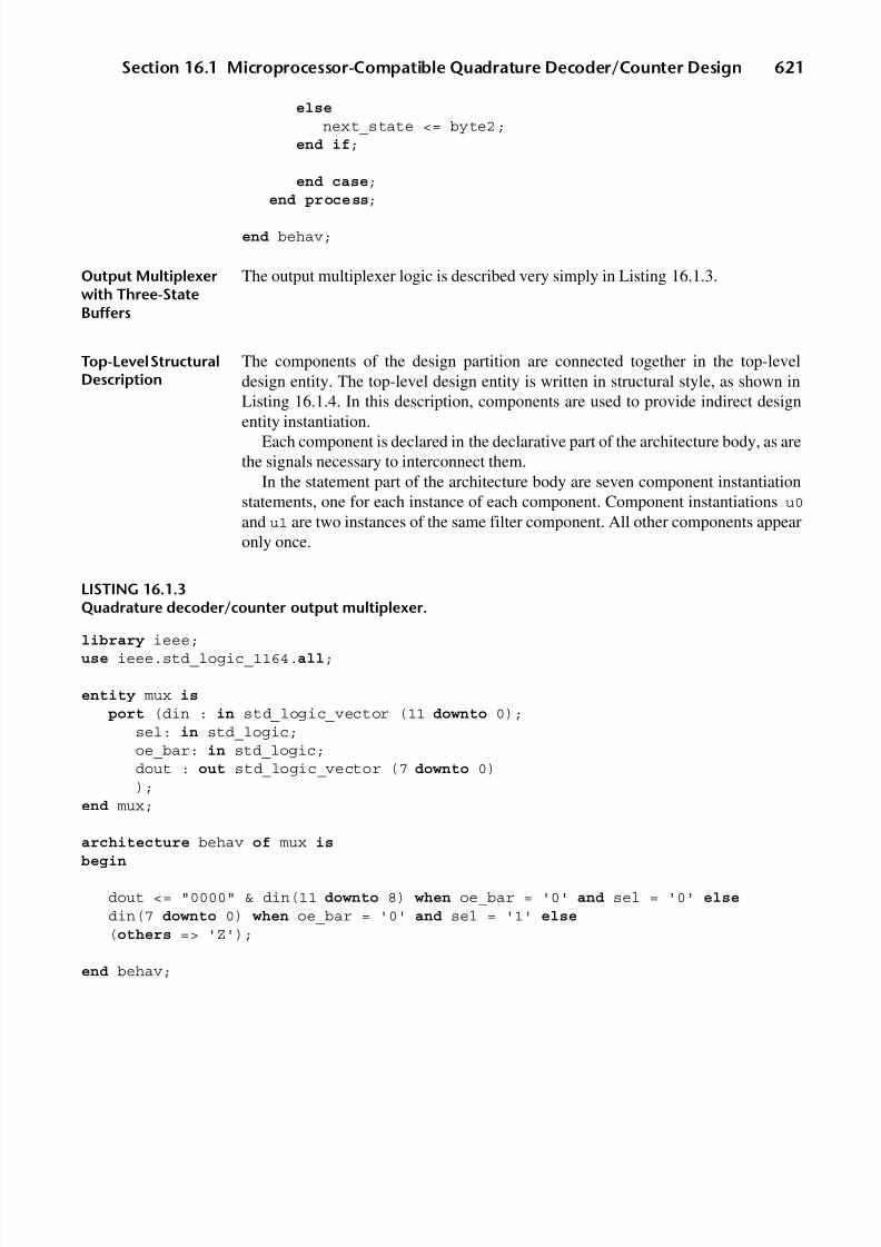
8/9/2019 VHDL for Engineers - Kenneth L. Short.pdf
http://slidepdf.com/reader/full/vhdl-for-engineers-kenneth-l-shortpdf 654/719
Section 16.1 Microprocessor-Compatible Quadrature Decoder/Counter Design 621
else
next_state <= byte2;end if;
end case;end process;
end behav;
Output Multiplexerwith Three-StateBuffers
The output multiplexer logic is described very simply in Listing 16.1.3.
Top-Level StructuralDescription
The components of the design partition are connected together in the top-leveldesign entity. The top-level design entity is written in structural style, as shown inListing 16.1.4. In this description, components are used to provide indirect design
entity instantiation.Each component is declared in the declarative part of the architecture body, as are
the signals necessary to interconnect them.In the statement part of the architecture body are seven component instantiation
statements, one for each instance of each component. Component instantiations u0
and u1 are two instances of the same filter component. All other components appearonly once.
LISTING 16.1.3Quadrature decoder/counter output multiplexer.
library ieee;use ieee.std_logic_1164.all;
entity mux is
port (din : in std_logic_vector (11 downto 0);sel: in std_logic;oe_bar: in std_logic;dout : out std_logic_vector (7 downto 0));
end mux;
architecture behav of mux isbegin
dout <= "0000" & din(11 downto 8) when oe_bar = '0' and sel = '0' else
din(7 downto 0) when oe_bar = '0' and sel = '1' else
(others => 'Z');
end behav;

8/9/2019 VHDL for Engineers - Kenneth L. Short.pdf
http://slidepdf.com/reader/full/vhdl-for-engineers-kenneth-l-shortpdf 655/719
622 Chapter 16 More Design Examples
LISTING 16.1.4Top-level structural description of quadrature decoder/counter.
library ieee;use ieee.std_logic_1164.all;
entity quad_decode isport (
ch_a: in std_logic;ch_b: in std_logic;rst_bar: in std_logic;clk: in std_logic;sel: in std_logic;oe_bar: in std_logic;d: out std_logic_vector (7 downto 0));
end quad_decode;
architecture structure of quad_decode is
component filterport (cx, clk, rst_bar : in std_logic;
y : out std_logic);end component;
component fx_decodeport (a, b, clk, rst_bar: in std_logic;
cnten, up: out std_logic);
end component;
component binary_cntrport (clk, cnten, up, rst_bar: in std_logic;
q: out std_logic_vector (11 downto 0));end component;
component double_buffport (din : in std_logic_vector (11 downto 0);
rst_bar: in std_logic;clk: in std_logic;inhibit: in std_logic;
dout : out std_logic_vector (11 downto 0));
end component;
component inhibit_fsmport (
rst_bar: in std_logic;clk: in std_logic;

8/9/2019 VHDL for Engineers - Kenneth L. Short.pdf
http://slidepdf.com/reader/full/vhdl-for-engineers-kenneth-l-shortpdf 656/719
Section 16.1 Microprocessor-Compatible Quadrature Decoder/Counter Design 623
sel: in std_logic;inhibit : out std_logic;oe_bar: in std_logic);
end component;
component muxport (din : in std_logic_vector (11 downto 0);
sel: in std_logic;oe_bar: in std_logic;dout : out std_logic_vector (7 downto 0));
end component;
signal ch_a_sig, ch_b_sig, cnten_sig, up_sig : std_logic;signal count_sig : std_logic_vector(11 downto 0);
signal dbl_buff_sig : std_logic_vector(11 downto 0);signal inhibit_sig : std_logic;
begin
u0: filter port map (cx => ch_a, clk => clk, rst_bar => rst_bar, y => ch_a_sig);
u1: filter port map (cx => ch_b, clk => clk, rst_bar => rst_bar, y => ch_b_sig);
u2: fx_decode port map (
a => ch_a_sig, b => ch_b_sig, clk =>clk, rst_bar => rst_bar,cnten => cnten_sig, up => up_sig);
u3: binary_cntr port map (clk => clk, cnten => cnten_sig, up => up_sig, rst_bar => rst_bar,q => count_sig);
u4: double_buff port map (din => count_sig, rst_bar => rst_bar, clk => clk, inhibit => inhibit_sig,dout => dbl_buff_sig);
u5: inhibit_fsm port map (rst_bar => rst_bar, clk => clk, sel => sel, inhibit => inhibit_sig,oe_bar => oe_bar);
u6: mux port map (din => dbl_buff_sig, sel => sel, oe_bar => oe_bar, dout => d);
end structure;

8/9/2019 VHDL for Engineers - Kenneth L. Short.pdf
http://slidepdf.com/reader/full/vhdl-for-engineers-kenneth-l-shortpdf 657/719
624 Chapter 16 More Design Examples
Since the names and interfaces of the design entities match those of the compo-nents, default binding is sufficient to fully configure the system and a configurationdeclaration is not necessary.
1 6. 2 VE RI FI CA TI ON OF QU AD RA TU RE D E C O D E R / C O U N T E R
After each component design entity in the quadrature decoder/counter wasdeveloped, it was independently verified using a separate testbench. When thesecomponents are reused by interconnecting them to form the quadrature decoder/ counter, a testbench must be written to verify the top-level structural description. Theresulting overall verification approach is bottom-up.
The verification plan for the top-level design entity is to generate the OSEquadrature phase signals A and B, which are inputs to the quadrature decoder/ counter, and to read the quadrature decoder/counter’s output to see if it has thecorrect count. To read the quadrature decoder/counter, the microprocessor busfunctional model (BFM) developed in Section 14.9 is used.
A testbench for the quadrature decoder/counter is given in Listing 16.2.1.
LISTING 16.2.1Testbench for quadrature decoder/counter.
library ieee;use ieee.std_logic_1164.all;
use bus_cycle.all;
entity quad_decode_tb is
end quad_decode_tb;
architecture tb_architecture of quad_decode_tb is
constant cpu_clk_period : time := 125 ns;constant a_b_clk_period : time := 1 ms;
-- Component declaration of the tested unitcomponent quad_decode
port(ch_a : in std_logic;ch_b : in std_logic;rst_bar : in std_logic;clk : in std_logic;sel : in std_logic;
8/9/2019 VHDL for Engineers - Kenneth L. Short.pdf
http://slidepdf.com/reader/full/vhdl-for-engineers-kenneth-l-shortpdf 658/719
Section 16.2 Verification of Quadrature Decoder/Counter 625
oe_bar : in std_logic;d : out std_logic_vector(7 downto 0) );
end component;
-- Stimulus signalssignal ch_a : std_logic;signal ch_b : std_logic;
-- Observed signalssignal addr_cpu: std_logic_vector (19 downto 0) := x"00000";signal data_cpu: std_logic_vector (7 downto 0) := "ZZZZZZZZ";signal wr_bar_cpu: std_logic := '1';signal rd_bar_cpu: std_logic := '1';signal clkout: std_logic;signal word_read : std_logic_vector (15 downto 0);signal cpu_reset_bar : std_logic;signal end_sim : boolean := false;
begin
-- Unit Under Test port mapUUT : quad_decodeport map
(ch_a => ch_a,ch_b => ch_b,rst_bar => cpu_reset_bar,clk => clkout,sel => addr_cpu(0),oe_bar => rd_bar_cpu,d => data_cpu);
cpu_clock_gen : process
begin
clkout <= '0';loop
wait for cpu_clk_period/2;clkout <= not clkout;exit when end_sim = true;
end loop; wait;
end process;
cpu_reset_gen : cpu_reset_bar <= '0', '1' after 2 * cpu_clk_period;
a_b_clk_gen : process -- Generate quadrature OSE outputsbegin
ch_a <= '0';(Cont.)

8/9/2019 VHDL for Engineers - Kenneth L. Short.pdf
http://slidepdf.com/reader/full/vhdl-for-engineers-kenneth-l-shortpdf 659/719
626 Chapter 16 More Design Examples
LISTING 16.2.1 (Cont.)
ch_b <= '0'; wait for a_b_clk_period/4;loop
exit when end_sim = true;ch_a <= '1'; wait for a_b_clk_period/4;ch_b <= '1'; wait for a_b_clk_period/4;ch_a <= '0'; wait for a_b_clk_period/4;ch_b <= '0'; wait for a_b_clk_period/4;
end loop; wait;
end process;
test : process
begin
for i in 1 to 4 loop
wait for 5 ms;read_cycle(x"08000", word_read(15 downto 8), 0, clkout, addr_cpu,
data_cpu, rd_bar_cpu);read_cycle(x"08001", word_read(7 downto 0), 0, clkout, addr_cpu,
data_cpu, rd_bar_cpu);end loop;end_sim <= true; wait;
end process;
end tb_architecture;
Constants are established for the CPU clock period (125 ns) and for the period of input waveforms A and B (1 ms). With A and B changing at this rate, we expect tohave 4 counts every millisecond.
The quad_decode component is declared in the declarative part of the archi-tecture body, as are the signals to connect it to the OSE output and microprocessorBFM.
Processes are included in the statement part of the architecture to generate theCPU clock and CPU reset. The microprocessor BFM procedures use this clock andreset, as does the quadrature decoder/counter. Process a_b_clk_gen generates theA and B waveforms.
During verification, the quadrature decoder/counter’s count must be read. Thisrequires that two addresses be read, corresponding to the high and low bytes of thecounter. For this simulation, addresses 08000 and 08001 are arbitrarily chosen.

8/9/2019 VHDL for Engineers - Kenneth L. Short.pdf
http://slidepdf.com/reader/full/vhdl-for-engineers-kenneth-l-shortpdf 660/719
Section 16.2 Verification of Quadrature Decoder/Counter 627
Accordingly, the BFM read procedure must be called twice, first with the address08000 and then with the address 08001. The first call reads the high byte and thesecond call reads the low byte.
The least significant bit of the address is connected to the sel input of thequadrature decoder/counter to determine which byte is being read. Since there are no
other devices connected to the simulated microprocessor’s bus, no other decodingof the address needs to be performed. As a result, input oe_bar of the quad-rature decoder/counter is connected directly to the read signal from the BFM(rd_cpu_ bar).
The verification process is named test. Many alternative strategies could beused for verification, including using assert statements in a loop to check the countread against the expected count. This testbench, however, focuses on whether boththe count logic and the inhibit logic of the quadrature decoder/counter work properlywhen interfaced to a microprocessor. Accordingly, a loop is used to read thequadrature decoder/counter’s count four times. Each read of the count is separatedby an interval of 5 ms. The output waveforms are examined to verify the result.
To verify the inhibit logic’s operation, the period of A and B and the reads are setso that the count is read at the same time that the counter is being incremented.
A portion of the output waveform around 5 ms is given in Figure 16.2.1. At5 ms (5000 us) B changes from 1 to 0. This should cause the count to incrementfrom 19 (decimal) to 20. At the same time B changes, the reading of the count isinitiated.
The change in B is processed by the filter component for channel B and does notappear at the input of the fx_decode component until 4½ clocks later. This is seenas the change in the ch_b_sig from 1 to 0. The fx_decode component assertscount enable (cnten) as a response. At the next triggering clock edge, the count in
the binary counter (q) is incremented to 14 hexadecimal (20 decimal).The reading of the quadrature decoder/counter starts at 5 ms, with the address
of the high byte of the count (08000 hexadecimal) becoming stable. Whenrd_bar_cpu goes low, the inhibit FSM (inhibit_fsm) asserts its inhibit signal sothat the register in the double_buff component does not store a copy of the countat subsequent triggering clock edges. As a result, when q increments to 14, thedouble buffer register is not enabled at the subsequent clock triggering edge and itsoutput dout continues to have the value 13.
The high byte read by the first call of the read_cycle procedure returns the highbyte count 00. The low byte read by the second call of the read_cycle procedurereturns the low byte count 13. As a result, the value read is the correct value of 13hexadecimal (19 decimal).
At the trailing edge of signal rd_bar_cpu during the second bus cycle, theinhibit control FSM unasserts inhibit. At the next triggering clock edge, theregister in double_buff stores a copy of the new count in binary_cntr.
Both the correct count and the proper operation of the quadrature encoder duringreading are verified by examination of these waveforms.

8/9/2019 VHDL for Engineers - Kenneth L. Short.pdf
http://slidepdf.com/reader/full/vhdl-for-engineers-kenneth-l-shortpdf 661/719
628 Chapter 16 More Design Examples
1 6. 3 P AR AM ET ER IZ ED Q UA DR AT UR E D E C O D E R / C O U N T E R
The quadrature decoder/counter and its testbench in the previous two sections arefor a design where the counter has a fixed width of 12 bits. This design can bechanged to one with a parameterized count width. To accomplish this, threecomponents have to be parametrized: the binary counter, the double buffer register,and the multiplexer.
A description of a parameterized binary counter was given in Listing 15.9.1. Adescription for a parameterized multiplexer was given in Listing 15.11.4. This leavesonly the need for a parameterized double buffer register, which can be easilyobtained by modifying Listing 16.1.1.
When entities binary_counter, double_buff, and mux are modified so thatthey all use the generic n, we only need to add a generic clause to the entity declaration
FIGURE 16.2.1
Reading quadrature decoder/counter output while count is being incremented.

8/9/2019 VHDL for Engineers - Kenneth L. Short.pdf
http://slidepdf.com/reader/full/vhdl-for-engineers-kenneth-l-shortpdf 662/719
Section 16.3 Parameterized Quadrature Decoder/Counter 629
for the top-level quad_decode to have a fully parameterized quadrature decoder/ counter.
entity quad_decode is
generic (n : positive := 12);port (... );
end quad_decode;
Testbench forParameterizedQuadratureDecoder/Counter
We can use generic n to parameterize the testbench for the parameterized quadraturedecoder/counter. The testbench entity declaration must be modified to includegeneric n in a formal generic clause:
entity quad_decode_tb is
generic (n : positive := 4);end quad_decode_tb;
In the testbench, the component declaration for quad_decode must include n as
a local generic:
component quad_decodegeneric (n : positive);port( ... );end component;
In the component instantiation for quad_decode, as the UUT in the testbencharchitecture body, the generic n of the component must be associated with thegeneric n declared in the testbench’s entity declaration:
UUT : quad_decode generic map (n => n) port map (...);
If the testbench is taken as the top level, we only need to change the defaultgeneric value assigned to n in the testbench’s entity declaration to simulate aquadrature decoder/counter of any desired counter size from 1 to 16 bits.
As a final example, we could use a configuration declaration to set the value of the generic n and simulate the configuration declaration (Listing 16.3.1).
LISTING 16.3.1Configuration declaration to assign a value to the generic n.
configuration config_quad_decode of quad_decode_tb is
for tb_architecturefor UUT : quad_decode use entity quad_decode
generic map (n => 6);end for;
end for;end config_quad_decode
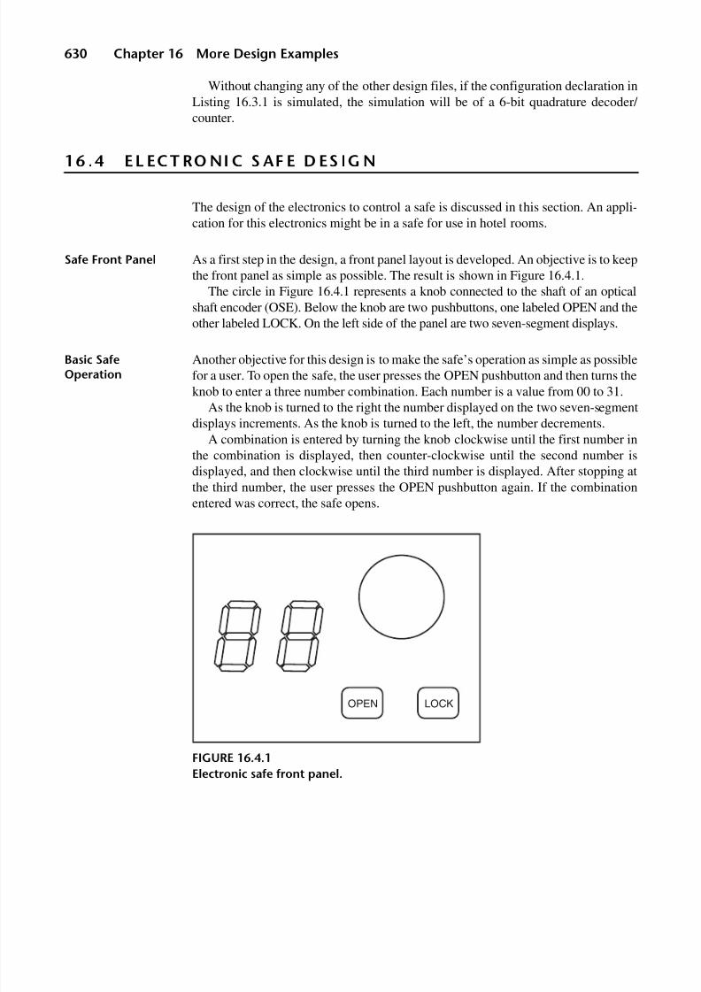
8/9/2019 VHDL for Engineers - Kenneth L. Short.pdf
http://slidepdf.com/reader/full/vhdl-for-engineers-kenneth-l-shortpdf 663/719
630 Chapter 16 More Design Examples
Without changing any of the other design files, if the configuration declaration inListing 16.3.1 is simulated, the simulation will be of a 6-bit quadrature decoder/ counter.
16 .4 E L EC T RO NI C S AF E D ES IG N
The design of the electronics to control a safe is discussed in this section. An appli-cation for this electronics might be in a safe for use in hotel rooms.
Safe Front Panel As a first step in the design, a front panel layout is developed. An objective is to keepthe front panel as simple as possible. The result is shown in Figure 16.4.1.
The circle in Figure 16.4.1 represents a knob connected to the shaft of an opticalshaft encoder (OSE). Below the knob are two pushbuttons, one labeled OPEN and theother labeled LOCK. On the left side of the panel are two seven-segment displays.
Basic SafeOperation
Another objective for this design is to make the safe’s operation as simple as possiblefor a user. To open the safe, the user presses the OPEN pushbutton and then turns theknob to enter a three number combination. Each number is a value from 00 to 31.
As the knob is turned to the right the number displayed on the two seven-segmentdisplays increments. As the knob is turned to the left, the number decrements.
A combination is entered by turning the knob clockwise until the first number inthe combination is displayed, then counter-clockwise until the second number isdisplayed, and then clockwise until the third number is displayed. After stopping atthe third number, the user presses the OPEN pushbutton again. If the combination
entered was correct, the safe opens.
FIGURE 16.4.1
Electronic safe front panel.
OPEN LOCK

8/9/2019 VHDL for Engineers - Kenneth L. Short.pdf
http://slidepdf.com/reader/full/vhdl-for-engineers-kenneth-l-shortpdf 664/719
Section 16.4 Electronic Safe Design 631
To close the safe, the user closes the safe door and then presses the LOCKpushbutton.
The Safe’sElectronics
The safe’s electronics receives inputs from the front panel and provides signals to theseven-segment displays and to a motorized bolt. When the bolt’s motor is actuated to
turn in one direction, it unlocks the safe door. When it is actuated to turn in the otherdirection, it locks the safe door.
The system’s input and output signals are given in the entity declaration for thetop-level design entity digital_lock in Listing 16.4.1.
For simplicity, input signals A and B from the OSE, lock_pb_bar andopen_pb_bar from the pushbuttons, and door_closed from a limit switch thatsenses when the safe door is closed, are all assumed to be bounce free.
Output port open_close controls the direction the motorized bolt is to bemoved. Output port actuate_lock provides a pulse of one state time duration thatcontrols when the bolt should be moved. The duration of this pulse would have to
be lengthened to accommodate the requirements of a particular motorized boltassembly.
Safe Block Diagram A block diagram of the safe’s electronics, corresponding to the first-level partition of the system, is given in Figure 16.4.2.
The first-level partition and its corresponding block diagram were determinedbased on the functions the system needs to perform. When the block diagram wasinitially drawn, all the inputs and outputs of the individual blocks were not known.As the individual blocks were further refined, additional input and output ports wereadded as needed. What is shown in Figure 16.4.2 is the final, completely definedblock diagram.
LISTING 16.4.1Entity declaration for electronic safe top-level design entity.
entity digital_lock is
port(clk : in std_logic; -- system clock rst_bar : in std_logic; -- system reseta : in std_logic; -- optical shaft encoder channel A b : in std_logic; -- optical shaft encoder channel Block_pb_bar : in std_logic; -- lock pushbutton
open_pb_bar : in std_logic; -- open pushbuttondoor_closed_bar : in std_logic; -- indicates safe door is closed actuate_lock : out std_logic; -- strobe to change bolt positionopen_close : out std_logic; -- direction to move locking boltseg_dig_0 : out std_logic_vector(6 downto 0); -- seg values for digit 0seg_dig_1 : out std_logic_vector(6 downto 0) -- seg value for digit 1);
end digital_lock;

8/9/2019 VHDL for Engineers - Kenneth L. Short.pdf
http://slidepdf.com/reader/full/vhdl-for-engineers-kenneth-l-shortpdf 665/719
6 3 2
FIGURE 16.4.2
Block diagram of electronic safe.
rst_barclk
ose_decoder_fsm
u0
master_fsm
bcd_2dec
u2
digit_compare
u3
u1
bcd_7seg
u4
u5
bcd_7seg
seg_dig_1[6:0][6:0]
seg_dig_0[6:0][6:0]
open_closeactuate_lock
_closed_baropen_pb_bar
lock_pb_bar
ba a
bclkrst_bar
cten_barup_bar
dir_chngd
clkrst_barcnt_en_bar
up_bardir_chngddoor_closed_bar
lock_pb_baropen_pb_barnum_eq
cnt_en_bar_fsmactuate_lockopen_close
blank_barclear_counters_bar
[1:0]num_sel[1:0]
clkrst_barup_bar
qbcd0[3:0][3:0]
[3:0]qbcd1[3:0]
[3:0]bcd0[3:0]
[3:0]bcd1[3:0]
[1:0]num_sel[1:0]
num_eq
bi_bar1 lt_bar
[3:0]dcba[3:0]
[6:0]seg[6:0]
bi_bar1 lt_bar[3:0]
dcba[3:0]
[6:0]seg[6:0]
cnt_en1_barcnt_en2_bar

8/9/2019 VHDL for Engineers - Kenneth L. Short.pdf
http://slidepdf.com/reader/full/vhdl-for-engineers-kenneth-l-shortpdf 666/719
Section 16.4 Electronic Safe Design 633
The block diagram consists of six component design entities:
• u0: ose_decoder_fsm
• u1: master_fsm
• u2: bcd_2dec
• u3: digit_compare
• u4 and u5: bcd_7seg
In developing the first-level partition, it is obvious that a two-digit modulo 32BCD counter is required to store the number to be displayed. In the block diagram,this counter is component u2, design entity bcd_2dec. The code for this counterwas given in Listing 9.4.7 (page 359). We are simply reusing it in this design.
A combinational circuit is required to convert each BCD digit from the two-digitmodulo 32 BCD counter to a seven-segment code to drive the correspondingseven-segment display. In the block diagram, these two decoders are two instances(u4 and u5) of the design entity bcd_7seg. The code for this decoder was given in
Listing 4.8.2 (page 146). We are simply reusing it in this design. The originaldecoder description includes a lamp test input named lt_bar that is not used in thisdesign. Accordingly, in the port maps for the instantiation of the two decoders thisinput is associated with the constant value '1', leaving it unasserted.
Safe’s Control The majority of new design effort for the safe electronics is in defining and imple-menting components u0 and u1, and, to a much lesser extent, u3. Design entities u0and u1 are both FSMs, which together control the operation of the system.
In theory the control portion of the electronic safe could be designed as a singleFSM. However, it simplifies defining the operation of the electronic safe to parti-
tion the control function into two cooperating FSMs. One FSM is componentose_decoder_fsm. It has limited and very specific functions. The other FSM iscomponent master_fsm. This FSM controls the overall operation of the safe.
OSE Decoder FSM We have previously considered the design of decoders for optical shaft encoders. See“Decoder for an Optical Shaft Encoder” on page 403. Since the OSE to be used inthis design generates 32 pulses per revolution, its resolution is ideal for this appli-cation and its decoder does not need to implement a 4 × resolution enhancement.
Our previous OSE decoders had two outputs, one to enable a counter to count andthe other to control count direction. However, for this application the OSE decoder
requires an additional output.When entering a number, the BCD counter is incremented or decremented as the
knob attached to the OSE is rotated. The value displayed on the seven-segmentdisplays corresponds to the counter’s value. The rate at which the knob is rotated andwhether the knob’s rotation is stopped one or more times before the desired numberis displayed cannot be restricted. So, an issue to be resolved is when the numberdisplayed is considered to be an entry.

8/9/2019 VHDL for Engineers - Kenneth L. Short.pdf
http://slidepdf.com/reader/full/vhdl-for-engineers-kenneth-l-shortpdf 667/719
634 Chapter 16 More Design Examples
One straightforward solution would be to add an ENTER pushbutton to the panel.With this pushbutton added, the procedure for user entry of a three-digit combinationwould be:
• Press the OPEN pushbutton to indicate the start of the entry of a combination
• Turn the knob clockwise until the first number of the combination is displayedand then press the ENTER pushbutton
• Turn the knob counter-clockwise until the second number of the combinationis displayed and then press the ENTER pushbutton
• Turn the knob clockwise until the third number of the combination is displayedand then press the OPEN pushbutton.
An alternative solution, one that eliminates the need for addition of an ENTERpushbutton, is to have the OSE decoder sense when the direction of rotation of theknob has changed and to generate a signal indicating a change in direction. Whenthis signal is asserted, master_fsm takes the number that is being displayed and
processes it as an entry. Using this approach, the procedure for the user to enter athree-digit combination is:
• Press the OPEN pushbutton to indicate the start of the entry of a combination
• Turn the knob clockwise until the first number of the combination is displayed
• Turn the knob counter-clockwise until the second number of the combinationis displayed
• Turn the knob clockwise until the third number of the combination is displayedand then press the OPEN pushbutton.
To implement this second approach, the OSE decoder must have an output thatindicates, for one state time, that the direction has changed. In the block diagram,ose_decoder_fsm has output dir_changed for this purpose.
Operation of OSEDecoder
Component ose_decoder_fsm detects the occurrence of a positive edge on input A.When such an edge is detected, ose_decoder_fsm examines the value of B todetermine the direction of rotation. A state diagram for ose_decoder_fsm is given inFigure 16.4.3.
When the system is reset, ose_decoder_fsm starts in state cw0. In this state, theFSM examines A on each triggering clock edge, waiting for A to be 0 as the first stepin detecting a positive edge on A. If A is 0, the FSM transitions to state cw1 at the nexttriggering clock edge. In state cw1, the FSM waits for A to be 1. If A is 1, the FSM
transitions to state cwpe at the next triggering clock edge. The fact that the FSM is instate cwpe indicates that a positive edge has just been detected on A.
In state cwpe, the FSM examines B to determine whether the knob’s rotation isclockwise (cw) or counter-clockwise (ccw). If B is 0, rotation is clockwise and theFSM transitions to state cwcnt. The FSM being in state cwcnt indicates that apositive edge has been detected on A with the knob being rotated clockwise. As aresult, in this state outputs cten_bar and up_bar are asserted.

8/9/2019 VHDL for Engineers - Kenneth L. Short.pdf
http://slidepdf.com/reader/full/vhdl-for-engineers-kenneth-l-shortpdf 668/719
Section 16.4 Electronic Safe Design 635
If in state cwpe the FSM examines B and it is a 1, the transition is to stateccwcnt. The FSM being in state ccwcnt indicates that a positive edge has beendetected on A while the knob is being rotated counter-clockwise. As a result, in this
state output cten_bar is asserted and output up_bar is unasserted.Outputs cten_bar and up_bar are asserted as a function of the present state
only and are, therefore, Moore outputs.If the knob is continually turned clockwise, the FSM cycles through the states
cw0, cw1, cwpe, cwcnt, and back to cw0. In contrast, if the knob is continuallyturned counter-clockwise, the FSM cycles through the states ccw0, ccw1, ccwpe,ccwcnt, and back to ccw0. Transition from one set of these states to the other
FIGURE 16.4.3
State diagram for OSE decoder FSM.
ccwcnt
null;
@ELSE
@ELSE
@ELSE
@ELSE
@ELSE
rst_bar ‘0’
cten_bar ‘0’.
up_bar ‘1’.
cw1
cwpe
cwcnt
cww0
cw0
cten_bar ‘0’;
up_bar ‘0’;
if b ‘0’ then
dir_chngd ‘1’.
end if;
if b‘1’ then
dir_chngd ‘1’.
end if;
null;
a ‘0’
b ‘0’
a ‘0’
a ‘1’
b ‘1’ a ‘1’
null;
@ELSE
ccw1
ccwpe
null;
8/9/2019 VHDL for Engineers - Kenneth L. Short.pdf
http://slidepdf.com/reader/full/vhdl-for-engineers-kenneth-l-shortpdf 669/719
636 Chapter 16 More Design Examples
occurs only from state cwpe or ccwpe. The two sets of states are mirror images, onefor each direction of rotation.
The code for the OSE decoder is given in Listing 16.4.2.
LISTING 16.4.2
Code for electronic safe ose_decoder_fsm.
library ieee;use ieee.std_logic_1164.all;
entity ose_decoder_fsm is
port(a : in std_logic;b : in std_logic;clk : in std_logic;rst_bar : in std_logic;cten_bar : out std_logic;
up_bar : out std_logic;dir_chngd : out std_logic);
end ose_decoder_fsm;
architecture fsm of ose_decoder_fsm is
type state is (cw0, cw1, cwpe, cwcnt, ccw0, ccw1, ccwpe, ccwcnt);signal ps, ns : state;
begin
state_reg: process (clk, rst_bar) -- state register process
beginif rising_edge(clk) then
if rst_bar = '0' then
ps <= cw0;else
ps <= ns;end if;
end if;end process;
next_state: process (ps, a, b) -- next state processbegin
case ps is
-- clockwise rotation when cw0 =>
if a = '0' then ns <= cw1;else ns <= cw0;end if;
when cw1 =>

8/9/2019 VHDL for Engineers - Kenneth L. Short.pdf
http://slidepdf.com/reader/full/vhdl-for-engineers-kenneth-l-shortpdf 670/719
Section 16.4 Electronic Safe Design 637
if a = '1' then ns <= cwpe;else ns <= cw1;end if;
when cwpe =>if b = '0' then ns <= cwcnt;else ns <= ccwcnt;end if;
when cwcnt =>ns <= cw0;
-- counterclockwise rotation when ccw0 =>
if a = '0' then ns <= ccw1;else ns <= ccw0;end if;
when ccw1 =>if a = '1' then ns <= ccwpe;else ns <= ccw1;end if;
when ccwpe =>if b = '1' then ns <= ccwcnt;else ns <= cwcnt;end if;
when ccwcnt =>ns <= ccw0;
end case;end process;
outputs: process (ps, a, b) -- output processbegin
cten_bar <= '1'; -- default output valuesup_bar <= '-';dir_chngd <= '0';
case ps is
when cwpe =>if b = '1' then
dir_chngd <= '1';end if;
(Cont.)

8/9/2019 VHDL for Engineers - Kenneth L. Short.pdf
http://slidepdf.com/reader/full/vhdl-for-engineers-kenneth-l-shortpdf 671/719
638 Chapter 16 More Design Examples
LISTING 16.4.2 (Cont.)
when cwcnt =>cten_bar <= '0';up_bar <= '0';
when ccwpe =>if b = '0' then
dir_chngd <= '1';end if;
when ccwcnt =>cten_bar <= '0';up_bar <= '1';
when cw0 | cw1 | ccw0 | ccw1 =>null;
end case;end process;
end fsm
At the beginning of the output process, the outputs are assigned default values.The conditions for asserting outputs cten_bar and up_bar are a function of thepresent state only, so they are, as previously stated, Moore outputs.
Direction ChangedOutput
Output dir_chngd is asserted as a function of both the present state and input B.Accordingly, dir_chngd is a Mealy output.
Digit CompareComponent
Two components of the safe remain to be discussed in greater detail,digit_compare and master_fsm. We consider digit_compare first.
It is clear that each time a number is entered as part of a combination, it must becompared to the correct number. The digit_compare component performs thiscomparison. The BCD outputs from the counter are input to digit_compare. Thistwo-digit BCD value is compared with one of three two-digit BCD constants declared indigit_compare. A 2-bit input named num_sel selects which of the three two-digitBCD constants is used in the comparison. Component master_fsm controls the value
of num_sel so that the appropriate two-digit BCD constant is selected for comparison.Component digit_compare is a combinational design entity. It is always
comparing its two-digit BCD input from the BCD counter with one of its storedtwo-digit BCD constants. Output num_eq is asserted whenever the BCD inputs areequal to the selected BCD constant. Component master_fsm must be designed toexamine the comparator’s output only in response to the entry of a number.
The code for digit_compare is given in Listing 16.4.3.

8/9/2019 VHDL for Engineers - Kenneth L. Short.pdf
http://slidepdf.com/reader/full/vhdl-for-engineers-kenneth-l-shortpdf 672/719
Section 16.4 Electronic Safe Design 639
LISTING 16.4.3Description of digit_compare design entity.
library ieee;use ieee.std_logic_1164.all;
entity digit_compare isport(
bcd0 : in std_logic_vector(3 downto 0); -- ls BCD digit from counter bcd1 : in std_logic_vector(3 downto 0); -- ms BCD digit from counter num_sel : in std_logic_vector(1 downto 0); -- number in combinationnum_eq : out std_logic -- compared values are equal);
end digit_compare;
architecture behavioral of digit_compare is
constant first_num : std_logic_vector(7 downto 0) := b"0000_0101";constant second_num : std_logic_vector(7 downto 0) := b"0001_0001";constant third_num : std_logic_vector(7 downto 0) := b"0000_1001";
begin
process (bcd0, bcd1, num_sel)begin
case num_sel is
when "00" =>if bcd1&bcd0 = first_num then
num_eq <= '1';else
num_eq <= '0';end if;
when "01" =>if bcd1&bcd0 = second_num then
num_eq <= '1';else
num_eq <= '0';end if;
when "10" =>if bcd1&bcd0 = third_num then
num_eq <= '1';else
num_eq <= '0';end if;
when others =>num_eq <= '0';
(Cont.)

8/9/2019 VHDL for Engineers - Kenneth L. Short.pdf
http://slidepdf.com/reader/full/vhdl-for-engineers-kenneth-l-shortpdf 673/719
640 Chapter 16 More Design Examples
LISTING 16.4.3 (Cont.)
end case;end process;
end behavioral;
The three numbers that comprise the combination are declared as the constantsfirst_num, second_num, and third_num. If we wished to change the safe’scombination we would have to change the values assigned to these constants.
Master FSM The overall operational characteristics of the safe are determined by componentmaster_fsm. If we are not designing the safe from a detailed specification we havesome choices in terms of the details of the system’s operation. For example, whenthe safe is locked, and after the safe has been opened, we can blank the display. Onlywhen the OPEN pushbutton is pressed at the start of the entry of a combination is thedisplay lighted. The display remains lighted until the OPEN pushbutton is pressedagain at the end of the entry of the combination.
Another important operational consideration is to not give any indication to the userthat the combination entered is incorrect until after the user has entered all threenumbers and pressed the OPEN key. Otherwise, it is possible for a user to determine thecombination in no more than 96 attempts, as opposed to no more than 32,768 attempts.
The description of master_fsm is given in Listing 16.4.4.A state diagram for master_fsm is given in Figure 16.4.4.
LISTING 16.4.4Description of the electronic safe’s master_fsm component.
library ieee;use ieee.std_logic_1164.all;
entity master_fsm is
port(clk : in std_logic; -- system clock rst_bar : in std_logic; -- system resetcnt_en_bar : in std_logic; -- cnt_en signal from ose_decoder_fsm up_bar : in std_logic; -- up signal from ose_decoder_fsm dir_chngd : in std_logic; -- dir_chngd signal from ose_decoder_fsm door_closed_bar : in std_logic; -- signal from door closed switch
lock_pb_bar : in std_logic; -- debounced signal from lock pushbuttonopen_pb_bar : in std_logic; -- debounced signal from open pushbuttonnum_eq : in std_logic; -- num_eq output of digit comparator cnt_en_bar_fsm : out std_logic; -- counter enable from master fsm actuate_lock : out std_logic; -- pulse to actuate lock open_close : out std_logic; -- control signal open lock when asserted num_sel : out std_logic_vector(1 downto 0); -- select combination number blank_bar : out std_logic; -- blank seven segment displays;

8/9/2019 VHDL for Engineers - Kenneth L. Short.pdf
http://slidepdf.com/reader/full/vhdl-for-engineers-kenneth-l-shortpdf 674/719
Section 16.4 Electronic Safe Design 641
clear_counters_bar : out std_logic -- clear the counters);
end master_fsm;
architecture behavioral of master_fsm is
type state is (locked, start, cw, first_ok, second_ok, third_ok, unlocked,bad_num, lock);
signal ps, ns : state;begin
state_reg: process (clk, rst_bar)begin
if rising_edge (clk) then
if rst_bar = '0' then
ps <= locked;else
ps <= ns;
end if;end if;
end process;
next_state: process (ps, cnt_en_bar, up_bar, dir_chngd, door_closed_bar,lock_pb_bar, open_pb_bar, num_eq)
begin
case ps is
when locked =>if open_pb_bar = '0' then -- open pushbutton pressed
ns <= start;else
ns <= locked;end if;
when start =>if cnt_en_bar = '0' and up_bar = '0' then -- cw rotation detected
ns <= cw;else
ns <= start;end if;
When cw =>
if dir_chngd = '1' and num_eq = '1' then -- good first number ns <= first_ok;
elsif dir_chngd = '1' and num_eq = '0' then -- bad first number ns <= bad_num;
else -- still waiting for first number ns <= cw;
end if;(Cont.)

8/9/2019 VHDL for Engineers - Kenneth L. Short.pdf
http://slidepdf.com/reader/full/vhdl-for-engineers-kenneth-l-shortpdf 675/719
642 Chapter 16 More Design Examples
LISTING 16.4.4 (Cont.)
When first_ok =>if dir_chngd = '1' and num_eq = '1' then -- good second number
ns <= second_ok;elsif dir_chngd = '1' and num_eq = '0' then -- bad second number
ns <= bad_num;else -- still waiting for second number
ns <= first_ok;end if;
When second_ok =>if open_pb_bar = '0' and num_eq = '1' then -- good third number
ns <= third_ok;elsif dir_chngd = '1' and num_eq = '0' then -- bad third number
ns <= bad_num;else -- still waiting for second number
ns <= second_ok;end if;
when third_ok => -- unlock the lock ns <= unlocked;
when unlocked => -- lock is unlocked if lock_pb_bar = '0' and door_closed_bar = '0' then
ns <= lock;else
ns <= unlocked;end if;
when lock => -- lock the lock ns <= locked;
when bad_num => -- a bad number has been received if open_pb_bar= '0' then
ns <= locked;else
ns <= bad_num;end if;
end case;end process;
outputs: process (ps, cnt_en_bar, up_bar, dir_chngd, door_closed_bar,lock_pb_bar, open_pb_bar, num_eq)
8/9/2019 VHDL for Engineers - Kenneth L. Short.pdf
http://slidepdf.com/reader/full/vhdl-for-engineers-kenneth-l-shortpdf 676/719
Section 16.4 Electronic Safe Design 643
begin
cnt_en_bar_fsm <= '0'; -- default output valuesactuate_lock <= '0';open_close <= '0';num_sel <= "--";blank_bar <= '1';clear_counters_bar <= '1';
case ps is
when locked =>blank_bar <= '0';cnt_en_bar_fsm <= '1';clear_counters_bar <= '0';
when start =>null;
When cw =>num_sel <= "00";
When first_ok =>num_sel <= "01";
When second_ok =>num_sel <= "10";
when third_ok =>actuate_lock <= '1';open_close <= '1';
when unlocked =>blank_bar <= '0';clear_counters_bar <= '0';
when lock =>if door_closed_bar = '0' then
actuate_lock <= '1';end if;
when bad_num =>
null;
end case;end process;
end behavioral;

8/9/2019 VHDL for Engineers - Kenneth L. Short.pdf
http://slidepdf.com/reader/full/vhdl-for-engineers-kenneth-l-shortpdf 677/719
644 Chapter 16 More Design Examples
1 6. 5 VE RI F I CA TI ON O F E LE CT R ON IC S AF E
A simple testbench for a nonexhaustive functional verification of the electronic safedesign is discussed in this section. This testbench can serve as the basis for a morecomprehensive testbench. The approach used is to create a testbench whose stimulusmodels user entry of a combination. The focus is on procedures that encapsulate thecode to generate OSE pulses corresponding to entry of a specific combination.Output waveforms from the simulation must be examined to determine if the combi-nation opens the safe.
FIGURE 16.4.4
State diagram for master_fsm.
@ELSE
@ELSE @ELSE
rst_bar ‘0’
open_pb_bar ‘0’
open_pb_bar
‘0’
dir _chngd ‘f’ and num_eq ‘0’
dir_chngd ‘f’ and num_eq ‘0’
dir_chngd ‘f’ and num_eq ‘0’
open_bp_bar ‘0’ and num_eq ‘0’
cnt_en_bar ‘0’ and up_bar ‘0’
dir_chngd ‘1’ and num_eq ‘1’
dir_chngd ‘1’ and num_eq ‘1’
lock_pb_bar ‘0’and door_closed_bar ‘0’
num_sel ‘--’;if door_closed_bar‘0’ then actuate_lock ‘1’;end if;
num_sel “”;blank_bar‘0’;cnt_en_bar_fsm‘1’;clear_counters_bar‘0’;
num_sel “”;null;
num_sel “--”;null;
num_sel “--”;num_sel “00”;
num_sel “--”;num_sel “01”;
num_sel “--”;num_sel “10”;
num_sel “”;actuate_lock ‘1’;open_close ‘1’;
num_sel “”;blank_bar ‘0’;
clear_counters bar ‘0’;
@ELSE
lock
locked
start
1
1
1
2
2
2
@ELSE
first_ok
@ELSE
second
_ok
cw
thrd_ok
@ELSE
unlocked
bad_nu

8/9/2019 VHDL for Engineers - Kenneth L. Short.pdf
http://slidepdf.com/reader/full/vhdl-for-engineers-kenneth-l-shortpdf 678/719
Section 16.5 Verification of Electronic Safe 645
LISTING 16.5.1Procedure to generate a specified number of pulses from an OSE.
procedure clock_gen (signal clk_a, clk_b: out std_logic; -- output signals from OSE constant period : in time; -- period of output signals
constant high : in time; -- pulse widthconstant phase : in time; -- phase between signalsconstant pulses : in integer; -- number of pulses to be generated constant cw : boolean) is -- direction of rotation simulated
begin
for i in 1 to pulses loop
if cw then
clk_a <= '1', '0' after high;clk_b <= '0', '1' after phase, '0' after phase + high;
else
clk_a <= '0', '1' after period - high;
clk_b <= '0', '1' after phase, '0' after phase + high;end if; wait for period;
end loop;end clock_gen;
Modeling the OSE’sOperation
Two procedures are used to model the output of the OSE corresponding to entry of acombination by a user. Procedure clock_gen generates a specified number of pulses on A and provides the appropriate phase relationship between A and B, basedon whether the knob is being turned clockwise or counter-clockwise. Code for this
procedure is given in Listing 16.5.1.Parameter pulses is an integer passed to the procedure to specify the number of pulses to be generated. Parameter cw is a boolean used to specify the direction of rotation. If cw is true, A leads B, otherwise A lags B. Each time through the loop, asingle pulse is generated on A and on B with the proper phase relationship.
A second procedure, rlr, has three parameters: right1, left1, and right2. Theseparameters correspond to the three numbers to be modeled as a user-entered combi-nation. Procedure rlr calls procedure clock_gen three times to generate the number of pulses that correspond to turning the OSE’s knob in the proper directions until each of the three numbers is displayed in order. Code for rlr is given in Listing 16.5.2.
LISTING 16.5.2Procedure to model user entry of a three-number combination.
procedure rlr (constant right1, left1, right2 : in integer) is
constant ose_period : time := 1000 ns;variable left1_pulses : integer := right1 + (32 - left1);variable right2_pulses : integer := (32 - left1) + right2 + 1;
(Cont.)

8/9/2019 VHDL for Engineers - Kenneth L. Short.pdf
http://slidepdf.com/reader/full/vhdl-for-engineers-kenneth-l-shortpdf 679/719
646 Chapter 16 More Design Examples
LISTING 16.5.2 (Cont.)
begin
wait for ose_period * 2;clock_gen (a,b, 1000 ns, 500 ns, 250 ns, right1, true); wait for ose_period * 2;clock_gen (a, b, 1000 ns, 500 ns, 250 ns, left1_pulses, false); wait for ose_period * 2;clock_gen (a, b, 1000 ns, 500 ns, 250 ns, right2_pulses, true); wait for ose_period;
end rlr;
The code for the testbench is given in Listing 16.5.3. Simulation of the testbenchgenerates the stimulus corresponding to user entry of a combination. The value of the combination is determined by the parameters in the call to procedure rlr. Tosave space, the text for procedures clock_gen and rlr, from Listings 16.5.1 and
16.5.2, have been removed from the testbench listing. Comments indicate wherethese procedures would appear. Alternatively, the procedures could be placed in apackage and compiled to a library.
LISTING 16.5.3Simple testbench for electronic safe design.
library ieee;use ieee.std_logic_1164.all;
entity digital_lock_tb is
end digital_lock_tb;
architecture tb_architecture of digital_lock_tb is
-- Stimulus signals - signals mapped to the input and inout ports of UUT signal clk : std_logic;signal rst_bar : std_logic;signal a : std_logic;signal b : std_logic;signal lock_pb_bar : std_logic;signal open_pb_bar : std_logic;
signal door_closed_bar : std_logic;-- Observed signals - signals mapped to the output ports of UUT signal actuate_lock : std_logic;signal open_close : std_logic;signal seg_dig_0 : std_logic_vector(6 downto 0);signal seg_dig_1 : std_logic_vector(6 downto 0);
signal lock_opened : std_logic := '0'; -- lock was successfully opened

8/9/2019 VHDL for Engineers - Kenneth L. Short.pdf
http://slidepdf.com/reader/full/vhdl-for-engineers-kenneth-l-shortpdf 680/719
Section 16.5 Verification of Electronic Safe 647
constant period : time := 100 ns;signal end_sim : boolean := false;
-- ** code for procedure clock_gen goes here **
-- ** code for procedure rlr goes here **
begin
-- Unit Under Test port mapUUT : entity digital_lockport map (
clk => clk,rst_bar => rst_bar,a => a,b => b,lock_pb_bar => lock_pb_bar,
open_pb_bar => open_pb_bar,door_closed_bar => door_closed_bar,actuate_lock => actuate_lock,open_close => open_close,seg_dig_0 => seg_dig_0,seg_dig_1 => seg_dig_1);
-- reset signalrst_bar <= '0', '1' after 5.7 * period;
-- system clock clock : process
begin
clk <= '0'; wait for period/2;loop
clk <= not clk; wait for period/2;exit when end_sim = true;
end loop; wait;
end process;
-- stimulus process to model entry of a combinationstim: process
constant ose_period : time := 1000 ns;begin
a <= '0'; -- initial values for signalsb <= '0';
(Cont.)

8/9/2019 VHDL for Engineers - Kenneth L. Short.pdf
http://slidepdf.com/reader/full/vhdl-for-engineers-kenneth-l-shortpdf 681/719
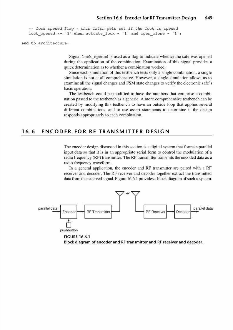
8/9/2019 VHDL for Engineers - Kenneth L. Short.pdf
http://slidepdf.com/reader/full/vhdl-for-engineers-kenneth-l-shortpdf 682/719
Section 16.6 Encoder for RF Transmitter Design 649
-- lock opened flag - this latch gets set if the lock is opened lock_opened <= '1' when actuate_lock = '1' and open_close = '1';
end tb_architecture;
Signal lock_opened is used as a flag to indicate whether the safe was openedduring the application of the combination. Examination of this signal provides aquick determination as to whether a combination worked.
Since each simulation of this testbench tests only a single combination, a singlesimulation is not at all comprehensive. However, a single simulation allows us toexamine all the signal changes and FSM state changes to verify the electronic safe’sbasic operation.
The testbench could be modified to have the numbers that comprise a combi-nation passed to the testbench as a generic. A more comprehensive testbench can becreated by modifying this testbench to have an outside loop that applies several
different combinations, and to use assert statements to determine if the designresponds appropriately to each combination.
1 6. 6 E NC OD ER FO R R F TR AN SM IT TE R D ES IG N
The encoder design discussed in this section is a digital system that formats parallelinput data so that it is in an appropriate serial form to control the modulation of aradio frequency (RF) transmitter. The RF transmitter transmits the encoded data as aradio frequency waveform.
In a general application, the encoder and RF transmitter are paired with a RFreceiver and decoder. The RF receiver and decoder together extract the transmitteddata from the received signal. Figure 16.6.1 provides a block diagram of such a system.
FIGURE 16.6.1
Block diagram of encoder and RF transmitter and RF receiver and decoder.
Encoder RF Transmitter RF Receiver Decoderparallel data
pushbutton
parallel data

8/9/2019 VHDL for Engineers - Kenneth L. Short.pdf
http://slidepdf.com/reader/full/vhdl-for-engineers-kenneth-l-shortpdf 683/719
650 Chapter 16 More Design Examples
A variety of different encoder/decoder IC pairs exist, each having different levelsof complexity and optimized for different RF modulation schemes. The encoder inthis section is for use with transmitters using amplitude shift keying (ASK)modulation. ASK transmitters simply turn their carrier frequency ON and OFF inresponse to a modulation signal. The output of the encoder is the modulation signal.
One of the simplest types of encoders for ASK modulation outputs an 8-bitaddress and 4 bits of data each time a transmit enable pushbutton is pressed. The8-bit address and 4-bit data values are parallel inputs to the encoder (Figure 16.6.2).The address and data are output from the encoder as a serial information word.
The address that is transmitted along with the data allows the decoder to onlyoutput data from an encoder that uses the same address.
A commercial encoder example is the Holtek HT12E. It is used in short-rangeremote control applications such as garage door openers, car door openers, andburglar alarm systems. The encoder designed here is functionally equivalent to theHT12E.
Top-level EncoderEntity
The entity declaration for the top-level entity rf_encoder is given in Listing 16.6.1.
Format ofInformation Word
The serial information word output from the encoder must be in the format shown inFigure 16.6.3. This format provides improved receiver performance.
LISTING 16.6.1Entity declaration for top-level encoder entity.
entity rf_encoder2 is
port( A : in std_logic_vector(7 downto 0); -- address bitsD : in std_logic_vector(3 downto 0); -- data bits (equiv to AD11:AD8)te_bar : in std_logic; -- transmit enable controlclk : in std_logic; -- clock rst_bar : in std_logic; -- active low system resetdout : out std_logic); -- serialized A0:A7 & D0:D7
end rf_encoder2;
FIGURE 16.6.2
Encoder inputs and outputs.
te_bar dout
A7-A0 D3-D0
Encoder

8/9/2019 VHDL for Engineers - Kenneth L. Short.pdf
http://slidepdf.com/reader/full/vhdl-for-engineers-kenneth-l-shortpdf 684/719
Section 16.6 Encoder for RF Transmitter Design 651
A bit time for this encoder is defined as being three system clock cycles long.Each information word starts with a pilot period that is 12 bit times (or 36 clock cycles) long. During the pilot period the encoder’s output is 0. Following the pilotperiod, the encoder’s output must be 1 for one clock cycle. This is the sync period.The address code period follows the sync period. During the address code period, the8 address bits are output (least significant bit first). Finally, during the data code
period, the 4 data bits are output (least significant bit first). The duration of thecombined address code and data code periods is 12 bit times.
Encoding Addressand Data Bits
The encoded form of each address bit and each data bit takes one bit time. The outputduring the first clock cycle of a bit time is always 0. The output during the second clock cycle is the complement of the address or data bit being encoded. The output duringthe third clock cycle is always a 1 (Figure 16.6.4). This form of pulse width modulation(PWM) encoding is used because the data slicer circuit in the RF receiver performsbetter when the RF transmitter is modulated this way, as opposed to when unencodeddata is directly used for modulation.
TransmissionTiming
When the transmit enable pushbutton is pressed, the encoder outputs an informationword. However, instead of a single copy of the information word being output inresponse to a single press of the transmit enable pushbutton, multiple copies are output.
Copies of the information word are output from the encoder in multiples of four. If the transmit enable pushbutton is released before the first four copies have been output,
FIGURE 16.6.3
Format of serial information word.
A0 A1 A2 A3 A4 A5 A6 A7 D0 D1 D2 D3
pilot period address code perioddata codeperiod
sync pulse
12 bit times 12 bit times
FIGURE 16.6.4
PWM coding of address and data bits.
system clock
logic 0
logic 1
bit time

8/9/2019 VHDL for Engineers - Kenneth L. Short.pdf
http://slidepdf.com/reader/full/vhdl-for-engineers-kenneth-l-shortpdf 685/719
652 Chapter 16 More Design Examples
the total number of copies output is four. If the transmit enable button is still pressed aftera multiple of four copies of the information word has been output, another multiple of four copies is output. This requirement is represented by the flowchart in Figure 16.6.5.
Design Approach The approach taken is to first design a system that can output a single copy of the
information word. This system consists of a data path and control. FSM fsm1 imple-ments the control. It has a send_word control input. When this input is asserted,fsm1 causes one copy of the information word to be output. After a copy of theinformation word has been output fsm1 asserts its word_done output.
Once a system that outputs a single copy of the information word was designedand verified, a second FSM that interacts with fsm1 was designed. This FSM,named te_fsm, monitors the transmit enable pushbutton. When this pushbutton ispressed, te_fsm causes fsm1 to output four copies of the information word byrepeatedly asserting fsm1’s send_word input and waiting for its word_done
response. FSM te_fsm then reexamines the transmit enable pushbutton; if it is stillpressed, te_fsm causes another four copies of the information word to be output.
Encoder First-levelPartition
The first-level partition of the encoder is shown in the block diagram in Figure 16.6.6.
FIGURE 16.6.5
Flowchart for transmission of information words.
Power on
No
No
Yes
Yes
Standby mode
Transmissionenabled ?
Transmissionstill enabled
4 data wordstransmitted
4 data wordstransmittedcontinuosly

8/9/2019 VHDL for Engineers - Kenneth L. Short.pdf
http://slidepdf.com/reader/full/vhdl-for-engineers-kenneth-l-shortpdf 686/719
6 5 3
FIGURE 16.6.6
First-level partition of RF encoder.
modulo_3_counter
u0
modulo_12_counter
u1
mux_12_to_1
u2
mux_3_to_1
u3
d_out
fsm1
u4
te_fsm
u5
[3:0]
[7:0]
[3:0]
[7:0]=1
=0
clear_bar
clkclk
rst_barrst_bar
In_bar
A[7:0]D[3:0]
force_0
force_2
mod_3_tc
[1:0]mod_3_cnt[1:0]
clear_barclk
rst_barcnt_en1
cnt_en2
mod_12_tc
mod_12_tc_m1
[3:0]mod_12_cnt[3:0]
input[11:0][3:0]
sel[3:0] mux_out
input[2:0][1:0]
sel[1:0] mux_out
send_word
mod_12_tcmod_12_tc_m1
mod_3_tc
clk
rst_bar
force_0force_2clear_bar
word_done
cnt_en2
rst_bar
clk
mod_3_tc
word_donete_bar
send_word

8/9/2019 VHDL for Engineers - Kenneth L. Short.pdf
http://slidepdf.com/reader/full/vhdl-for-engineers-kenneth-l-shortpdf 687/719
654 Chapter 16 More Design Examples
The system has six components:
u0: modulo_3_counteru1: modulo_12_counteru2: mux_12_to_1u3: mux_3_to_1u4: fsm1u5: te_fsm
fsm1 The overall function of fsm1 was discussed in previous paragraphs. The communi-cation between fsm1 and te_fsm is accomplished using the signals send_word andword_done. When te_fsm wants an information word output, it asserts itssend_word output. In response, fsm1 outputs one information word as describedabove. FSM fsm1 asserts its word_done output to signal te_fsm that it hascompleted outputting a copy of the information word.
The state diagram for fsm1 is given in Figure 16.6.7. In the idle state, fsm1
waits for te_fsm to request that an information word be output. When this request isreceived, fsm1 transitions to state pilot. It remains in state pilot until the pilotperiod ends. The end of the pilot period is indicated by the modulo 12 counter andthe modulo 3 counter simultaneously reaching their terminal counts.
At the end of the pilot period, fsm1 transitions to state synch where the syncpulse is output. It remains in this state for one system clock cycle, and then uncondi-tionally transitions to state A0_D2. While in state A0_D2, the 8 address bits and thefirst three of the 4 data bits are output.
After the third data bit has been output, fsm1 transitions to state D3. It remains inthis state for one bit time. While in state D3, the fourth data bit is output and
word_done is asserted. If te_fsm has requested that another word be sent beforethe end of the bit time, fsm1 transitions to state pilot. Otherwise, fsm1 transitionsback to the state idle.
Output word_done is asserted immediately upon entering state D3. This allowste_fsm three system clocks in which to examine the transmit enable pushbutton’soutput and assert send_word, if another information word is to be output. Assertingword_done early in this manner allows information words to be sent with no delaybetween them.
Functions of the
Components
The basic functions accomplished by each component are summarized in the
paragraphs that follow.
Modulo_3_Counter
Since a bit time is three system clocks long, a frequency divider is used to divide thesystem clock by three to provide a signal with a period equal to the bit time.Component modulo_3_counter serves this purpose. It provides a terminal countoutput mod_3_tc that is asserted every third system clock.

8/9/2019 VHDL for Engineers - Kenneth L. Short.pdf
http://slidepdf.com/reader/full/vhdl-for-engineers-kenneth-l-shortpdf 688/719
Section 16.6 Encoder for RF Transmitter Design 655
In addition to its terminal count output, modulo_3_counter provides a 2-bitoutput mod_3_cnt that indicates the current system clock in a bit time. There arealso two control inputs, force_0 and force_2, that, when asserted, force outputmod_3_cnt to be either "00" or "10", respectively.
FIGURE 16.6.7
State diagram for FSM fsm1.
1
2
idle
pilot
AD_D2
@ELSE
force_0 ‘1’;
force_2 ‘0’;
clear_bar ‘1’;
word_done ‘0’;
cnt_en2 ‘1’;
force_0 ‘1’;
force_2 ‘0’;
clear_bar ‘0’;
word_done ‘1’;
cnt_en2 ‘0’;
force_0 ‘0’;
force_2 ‘0’;
clear_bar ‘1’;
word_done ‘1’;
cnt_en2 ‘1’;
force_0 ‘0’;
force_2 ‘1’;
clear_bar ‘0’;
word_done ‘0’;
cnt_en2 ‘0’;
force_0 ‘0’;
force_2 ‘0’;
clear_bar ‘1’;
word_done ‘0’;
cnt_en2 ‘1’;
rst_bar ‘0’
send_word ‘0’ and mod_3_tc ‘1’
send_word ‘1’
D3
synch
@ELSE
@ELSE
@ELSE
send_word ‘1’ and mod_3_tc ‘1’
mod_12_tc ‘1’ and mod_3_tc ‘1’
mod_12_tc_m1 ‘1’ and mod_3_tc ‘1’

8/9/2019 VHDL for Engineers - Kenneth L. Short.pdf
http://slidepdf.com/reader/full/vhdl-for-engineers-kenneth-l-shortpdf 689/719
656 Chapter 16 More Design Examples
Mux_3_to_1 The output of mux_3_to_1 is the output dout of the encoder. One of the purposesof this multiplexer is to PWM encode each address and data bit. Output mod_3_cntfrom modulo_3_counter provides the select inputs to mux_3_to_1. Whenmod_3_cnt is "00", dout is '0'. When mod_3_cnt is "01", dout is thecomplement of the output of mux_12_to_1. The output of mux_12_to_1 is the
address or data bit to be encoded. When mod_3_cnt is "10", dout is "1".Sequencing the select inputs of mux_3_to_1 through "00", "01", and "10"
causes the multiplexer to output the PWM encoded form of the value at the output of mux_12_to_1.
Modulo_12_Counter
Component modulo_12_counter is used to time the pilot period and the combinedaddress code and data code periods. It uses the terminal count signal frommodulo_3_counter as one of its enable inputs, and an output from fsm1 as itsother enable input, to control when it counts a triggering edge of the system clock.
Pilot Period The pilot period is 12 bit times (36 clocks) long. In state idle, fsm1 clears
modulo_12_counter and modulo_3_counter. Clearing modulo_3_counterforces its output mod_3_cnt to be "00". This in turn forces dout from mux_3_
to_1 to be '0'. In state pilot component, fsm1 then enables modulo_
12_counter to count. When the pilot period is complete (12 bit times later),modulo_12_counter’s terminal count, mod_12_tc, is asserted. FSM fsm1
monitors mod_12_tc to determine when the pilot period is over.
Sync Period After the pilot period ends, fsm1 unasserts the force_0 input to mux_3_to_1 andasserts it force_2 input for one clock cycle. This causes dout of mux_3_to_1 tobe '1', thus generating the sync period.
Mux_12_to_1 The 12 data inputs to mux_12_to_1 are the 8 address bits and the 4 data bits that areto be encoded. If the select inputs to this multiplexer are sequenced from 0 to 11, themultiplexer outputs the address bits, in order from A0 to A11, and then the data bits,in order from D0 to D3.
The select inputs of mux_12_to_1 are driven by the 4-bit output mod_12_cnt of modulo_12_counter.
Sending Addressand Data Values
After the sync period, fsm1 clears modulo_12_counter and enables it to count outthe 12 bit times of the combined address code and data code periods. During each of these bit times, modulo_3_counter sequences the select inputs of mux_3_to_1 to
PWM encode each bit from mux_12_to_1’s output.
Te_fsm Component te_fsm is the master FSM for this design. However, it is much simplerin operation than fsm1. It monitors an input from the transmit enable pushbutton andthe word_done signal from fsm1. Its only output is the send_word signal thatcauses fsm1 to send an information word.
If it were desired to change the number of information words output in response tothe transmit enable pushbutton being pressed, only te_fsm would require modification.

8/9/2019 VHDL for Engineers - Kenneth L. Short.pdf
http://slidepdf.com/reader/full/vhdl-for-engineers-kenneth-l-shortpdf 690/719
Problems 657
PROBLE MS
16.1 Modify Listing 16.1.1 to generate a parameterized double buffer that can be used as acomponent in the parameterized version of the quadrature decoder/counter.
16.2 Modify the state diagram in Figure 16.4.4 so that it is appropriate for the version of the
electronic safe that has an added ENTER pushbutton. What other changes would be necessaryin the design for this version?
16.3 Discuss an approach to modify the electronic safe design so that the actuate_lock outputhas a pulse duration of 1 second.
16.4 Discuss an approach to modify the electronic safe design so that the actuate_lock outputis asserted until either a signal bolt_open from the motorized bolt is asserted when openingthe lock or a signal bolt_closed from the motorized bolt is asserted when closing the lock.
16.5 Assuming that the signals from the two pushbuttons on the safe’s front panel are not debounced,discuss how you would go about debouncing these signals using logic inside a PLD.
16.6 Determine the minimum system clock frequency for the electronic safe as a multiple of the
maximum frequency of signal A from the OSE.
16.7 Examine the code for procedure clock_gen in Listing 16.5.1. Draw and annotate thewaveforms A and B for one iteration of the loop when cw is true and one iteration of the loopwhen it is false.
16.8 Write a testbench to verify the design entity ose_decoder_fsm in Listing 16.4.2.
16.9 Write a structural style description for a system named incr_decr_digit. This systemtakes inputs from an OSE and, based on the direction of the OSE’s rotation, increments ordecrements the value displayed on a single seven-segment display. This design uses theose_decoder_fsm entity in Listing 16.4.2 as a component, along with the bcd_cntrentity in Problem 9.21 and bcd_7seg entity in Listing 4.8.2. A simplified block diagram of
this system is:
Write a testbench to verify your incr_decr_digit top-level design.
16.10 Examine the code for procedure rlr in Listing 16.5.2. Explain why the values for variablesleft1_pulses and right2_pulses are calculated as shown in the code. For a call torlr with parameters 5, 11, and 9, how many pulses will be generated on A for each directionof rotation?
incr_decr_digit
bcd_7seg
7
s e g m e n t s
bcd_cntrose_decoder_fsm
OSE

8/9/2019 VHDL for Engineers - Kenneth L. Short.pdf
http://slidepdf.com/reader/full/vhdl-for-engineers-kenneth-l-shortpdf 691/719
This page intentionally left blank

8/9/2019 VHDL for Engineers - Kenneth L. Short.pdf
http://slidepdf.com/reader/full/vhdl-for-engineers-kenneth-l-shortpdf 692/719
659
Appendix
VHDL Attributes
This appendix provides information on the predefined attributes of VHDL. Predefined
attributes denote values, functions, types, and ranges associated with various kinds of
named entities.
The table lists those prefixes for which the attribute is defined. T represents a type
and X represents a value of the type.
Table A.1
Type attributes.
Attribute Prefix Result
T’base Any type or subtype T Base of type T
T’left Any scalar type or subtype T The left bound of T
T’right Any scalar type or subtype T The right bound of T
T’high Any scalar type or subtype T The upper bound of T
T’low Any scalar type or subtype T The lower bound of T
T’ascending Any scalar type or subtype T True if T is defined with an ascending range,
otherwise false
T’image(X) Any scalar type or subtype T String representation of X
T’value(X) Any scalar type or subtype T The value of T whose string representation
is given by X
(Cont.)

8/9/2019 VHDL for Engineers - Kenneth L. Short.pdf
http://slidepdf.com/reader/full/vhdl-for-engineers-kenneth-l-shortpdf 693/719
660 Appendix VHDL Attributes
Table A.1 (Cont.)
Attribute Prefix Result
T’pos(X) Any discrete or physical typeor subtype T
The position number of X
T’val(X) Any discrete or physical typeor subtype T
The value whose position number is theuniversal integer value corresponding to X
T’succ(X) Any discrete or physical typeor subtype T
The value whose position number is onegreater than that of X
T’pred(X) Any discrete or physical typeor subtype T
The value whose position number is one lessthan that of X
T’leftof(X) Any discrete or physical typeor subtype T
The value to the left of X in the range of T
T’rightof(X) Any discrete or physical type
or subtype T
The value to the right of X in the range of T
Table A.2Array attributes.
Attribute Prefix Result
A’left[(N)] Array or array subtype Left bound of the Nth index of A
A’right[(N)] Array or array subtype Right bound of the Nth index of A
A’high[(N)] Array or array subtype Upper bound of the Nth index of A
A’low[(N)] Array or array subtype Lower bound of the Nth index of A
A’range[(N)] Array or array subtype The range A’left(N) to A’right(N) if theNth index range of A is ascendingor the range A’left(N) down toA’right(N) if the Nth index rangeof A is descending
A’reverse_range[(N)] Array or array subtype The range A’right(N) down to A’left(N)if the Nth index range of A isascending or the range A’right(N)
to A’Left(N) if the Nth index rangeis descending
A’length[(N)] Array or array subtype Number of values in the Nth index rangeof A
A’ascending[(N)] Array or array subtype True if the Nth index range of A isdefined with an ascending range,false otherwise

8/9/2019 VHDL for Engineers - Kenneth L. Short.pdf
http://slidepdf.com/reader/full/vhdl-for-engineers-kenneth-l-shortpdf 694/719
Appendix VHDL Attributes 661
Table A.3VHDL predefined signal attributes.
Attribute Result
S’Delayed(t) Implicit signal equivalent to S, but delayed t units of time
S’Stable(t) Implicit boolean signal; true when no event has occurred on S for t timeunits up to the current time, False otherwise
S’Quiet(t) Implicit boolean signal; True when no transaction has occurred on S for ttime units up to the current time, False otherwise
S’Transaction Implicit bit signal whose value is changed in each simulation cycle inwhich a transaction occurs on S (signal S becomes active)
S’Event A boolean value; true if an event has occurred on S in the currentsimulation cycle, False otherwise
S’Active A boolean value; true if a transaction occurred on S in the currentsimulation cycle, False otherwise
S’Last_event Amount of elapsed time since last event on S; if no event has yet occurredit returns Time’High
S’Last_active Amount of time elapsed since last transaction on S; if no event has yetoccurred it returns Time’High
S’Last_value Previous value of S before last event on S
S’Driving True if the process is driving S or every element of a composite S, or Falseif the current value of the driver for S or any element of S in the processis determined by the null transaction
S’Driving_value Current value of the driver for S in the process containing the assignmentstatement to S
Table A.4E attributes.
Attribute Prefix Result
E’simple_name Any named entity The simple name, character literal, or operator symbol of the
named entity
E’instance_name Any named entity other than thelocal ports and generics of acomponent declaration
A string describing the hierarchical path starting at the root ofthe design hierarchy and descending to the named entity,including the names of instantiated design entities
E’path_name Any named entity other than thelocal ports and generics of acomponent declaration
A string describing the hierarchical path starting at the root ofthe design hierarchy and descending to the named entity,excluding the names of instantiated design entities

8/9/2019 VHDL for Engineers - Kenneth L. Short.pdf
http://slidepdf.com/reader/full/vhdl-for-engineers-kenneth-l-shortpdf 695/719
This page intentionally left blank

8/9/2019 VHDL for Engineers - Kenneth L. Short.pdf
http://slidepdf.com/reader/full/vhdl-for-engineers-kenneth-l-shortpdf 696/719
663
Bibliography
Alfke, P. “Set-up and Hold Times,” Xilinx XAPP 095, November, 24 1997.Ashenden, P. J. The Designer's Guide to VHDL, 2nd ed. San Francisco: Morgan
Kaufmann Publishers, Inc., 2002.Bergeron, J. Writing Testbenches. Boston: Kluwer Academic Publishers, 2000.Brown, S. D. Field-Programmable Devices, 2nd ed. Los Gatos, CA: Stan Baker
Associates, 1995.Chang, K. C. Digital Design and Modeling with VHDL and Synthesis. Los Alamitos,
CA: IEEE Computer Society Press, 1997.Chang, K. C. Digital Systems Design with VHDL and Synthesis: An Integrated
Approach. Los Alamitos, CA: IEEE Computer Society, 1999.Cohen, B. VHDL Coding Styles and Methodologies. Boston: Kluwer AcademicPublishers, 1995.
Cohen, B. VHDL Answers to Frequently Asked Questions, 2nd ed. Boston: KluwerAcademic Publishers, 1998.
Cohen, B. Real Chip Design and Verification Using Verilog and VHDL. Palos VerdesPeninsula, CA: VhdlCohen Publishing, 2002.
Dewey, A. Analysis and Design of Digital Systems with VHDL. Boston: PWSPublishing Company, 1997.
EIA, Library of Parameterized Modules (LPM). Englewood, CO: GlobalEngineering Documents, 1996.
Elliot, J. P. Understanding Behavioral Synthesis: A Practical Guide to High-Level Design. Kluwer Academic Publishers, 1999.
Habinc, S. “VHDL Models for Board Level Simulation,” European Space Agency,Noordwidjk, The Netherlands, February 1996.
Habinc, S. and P. Sinander, “Using VHDL for Board Level Simulation,” IEEE Designand Test of Computers, 1996.
IEEE. “IEEE Standard Multivalued Logic System for VHDL Model Interoperability”(IEEE Std 1164-1993), 1993 ed. New York: Institute of Electrical andElectronics Engineers, 1993.

8/9/2019 VHDL for Engineers - Kenneth L. Short.pdf
http://slidepdf.com/reader/full/vhdl-for-engineers-kenneth-l-shortpdf 697/719
664 Bibliography
IEEE. “IEEE Standard for VITAL Application-Specific Integrated Circuit (ASIC)Modeling Specification” (IEEE Std 1076.4-1995), New York: Institute ofElectrical and Electronics Engineers, 1995.
IEEE. “IEEE Standard VHDL Mathematical Packages” (IEEE Std 1076.2-1996),New York: Institute of Electrical and Electronics Engineers, 1996.
IEEE. “IEEE Standard VHDL Synthesis Packages” (IEEE Std 1076.3-1997). NewYork: Institute of Electrical and Electronics Engineers, 1997.
IEEE. “IEEE Standard for VHDL Waveform and Vector Exchange (WAVES) toSupport Design and Test Verification” (IEEE Std 1029.1-1998), New York:Institute of Electrical and Electronics Engineers, 1998.
IEEE. “IEEE Standard for VHDL Register Transfer Level (RTL) Synthesis” (IEEEStd 1076.6-2004). New York: Institute of Electrical and ElectronicsEngineers, 2000.
IEEE. “IEEE Standard for Standard Delay Format (SDF) for the Electronic DesignProcess” (IEEE Std 1497-2001), New York: Institute of Electrical andElectronics Engineers, 2001.
IEEE. “IEEE Standard VHDL Language Reference Manual,” 2000 ed. New York:
Institute of Electrical and Electronic Engineers, 2002.Keating M. and P. Bricaud, Reuse Methodology Manual for System-On-A-Chip Designs, 3rd ed. Norwell, MA: Kluwer Academic Publishers, 2002.
Landis, D. L. “Programmable Logic and Application-Specific Integrated Circuits,” in Active Electronic Component Handbook . C. A. Harpa and H. C. Jones, eds.2nd ed. New York: McGraw-Hill, 1996.
Lee, S. Design of Computers and Other Complex Digital Devices. Upper SaddleRiver, NJ: Prentice Hall, 2000.
Maxfield, C. The Design Warrior's Guide to FPGAs. Burlington, MA: Newnes, 2004.Munden, R. ASIC & FPGA Verification: A Guide to Component Modeling. San
Francisco: Morgan Kaufmann Publishers, Inc., 2005.Parnell K. and N. Mehta, Programmable Logic Design Quick Start Hand Book ,
2nd ed. San Jose, CA: Xilinx, 2002.

8/9/2019 VHDL for Engineers - Kenneth L. Short.pdf
http://slidepdf.com/reader/full/vhdl-for-engineers-kenneth-l-shortpdf 698/719
665
Index
Symbols::= syntax replacement symbol, 47:= initial value, 87:= variable assignment, 186<= less than or equal, 134<= signal assignment, 9<> box, 101=> arrow, 61
[ ] square brackets, 48{ } braces, 48| vertical bar, 48, 106
Numerics22V10 SPLD, 21, 2474F539 decoder, 175, 27674HC138 decoder, 14574HC148 priority encoder, 13974HC153 multiplexer, 12874HC574 octal D flip-flop, 339
74LS221 retriggerable single shot, 36280C188EB microprocessor, 553
Aabstract type, 116abstraction
level of, 2, 38, 44, 56, 69, 431, 433, 552
accesstype, 83
active clock edge, 308active processes queue, 212Active-HDL, 36actual
associated with a port, 595actual parameter
function, 477
after clause, 257aggregate, 105
as an assignment target, 107used to combine scalars, 106using a distinct range in, 106
Aldec, 36algorithm, 431algorithmic state machine (ASM), 432algorithmic state machine chart (ASM chart), 432
ASM block, 434
basic elements, 432conditional output box, 434converting to VHDL, 438decision box, 434entrance path, 432exit path, 432state box, 432versus state diagram, 437

8/9/2019 VHDL for Engineers - Kenneth L. Short.pdf
http://slidepdf.com/reader/full/vhdl-for-engineers-kenneth-l-shortpdf 699/719
666 Index
alias, 514amplitude shift keying, 650analog-to-digital converter (ADC),
445analyzer, 10
AND array, 19anonymous type, 112architecture
behvioral style, 165body, 9, 53dataflow style, 127declarative part, 54specified in an entity name, 579statement part, 54
areadefinition of, 27synthesis constraint, 68
arithmetic operatorfor types unsigned and signed, 108in counter descriptions, 349on physcial types, 260
arrayattribute, 484logical operation on, 126matching elements, 126normalization in a function, 487, 514
ordering of elements, 134relational operation on, 133selecting elements, 104slice, 104treated as a single object, 104type, 101unconstrained, 101
arrow symbol, 61ascending range, 102ASM block, 434aspect ratio, 371assertion
concurrent statement, 268in timing verification, 287sequential statement, 265violation, 266
associative property, 125associativity of logical operator, 125
asynchronousassignment, 309input, 308input data, 334sequential circuit, 381
attributearray, 484definition of, 241event, 316image, 267predefined, 242quiet, 288range, 243stable, 316syn_encoding, 417user defined, 33
Bback annotation, 290base type, 92based literal, 115BCD counter, 356BCD to seven-segment decoder, 146behavior
definition, 69versus structure, 65
behavioralstyle architecture, 55, 57, 165synthesizer, 70
binary code, 409bind, 63binding
alternatives, 582default, 583definition of, 578indication, 583
information, 583bit string literal, 111bit_vector, 101block RAM, 374bottom-up
implementation, 71, 568verification, 569
branch coverage, 284

8/9/2019 VHDL for Engineers - Kenneth L. Short.pdf
http://slidepdf.com/reader/full/vhdl-for-engineers-kenneth-l-shortpdf 700/719
Index 667
buffer mode, 53built-in type, 89bus
contention, 95, 153functional model (BFM), 552
bused signal, 98
Ccase
choice, 172expression, 172others choice, 172
case sensitivity, 50case statement, 171character
literal, 99string literal, 110type, 90
characteristic equation, 328chip report, 33choice
in a case statement, 172in a selected signal assignment, 130
class, 82cleared, 305clock
active edge, 308cycle, 306duty cycle, 306edge detection, 315frequency, 306IEEE Std 1076.6 compliant, 306in a testbench, 527negative edge conditions, 316nonperiodic, 306period, 306periodic, 306positive edge conditions, 315signal, 306to output delay, 333triggering edge, 308width, 306, 332
closed subtype, 513closely related type, 109, 494
codecoverage, 281reuse, 370
Code2Graphics, 396coding style
behavioral, 57dataflow, 9, 56definition of, 55mixed, 65structural, 58, 577versus synthesis results, 66
combinationalactive-high output, 23active-low output, 23feedback, 382system, 123
combinational designbehavioral, 165dataflow style, 123
combinational loopavoiding, 155broken by a register, 382definition of, 155simulation cycle, 235synthesizer warning, 190
command line simulation, 12
comment, 7communicating processes, 167compilation
design description, 10order, 576
compilerFSM, 413
complex PLD (CPLD), 19component
configuration, 588connections, 594declaration, 64, 581definition, 62indirect design entity instantiation, 580instantiation, 60port connections, 594specification, 583to component connections, 596

8/9/2019 VHDL for Engineers - Kenneth L. Short.pdf
http://slidepdf.com/reader/full/vhdl-for-engineers-kenneth-l-shortpdf 701/719
668 Index
compositeconstant, 112literal, 110type, 83, 100
compound delimiter, 9
concatenation operator, 107concurrent
event, 3procedure call, 483signal assignment statement, 9
concurrent statementassertion statement, 268execution order, 10
concurrent subprogram call, 470condition, 132conditional
output box, 434signal assignment statement, 134
conditional signal assignment, 134
configurationbits, 22declaration, 587file, 34specification, 583
configuration declaration
for a testbench, 588multilevel hierarchies, 591
constantcomposite, 112deferred, 99, 504definition of, 99fully specified, 504object class, 83scalar, 99visibility, 100
constrained array, 103construct
accepted by synthesizer, 48definition of, 2ignored by synthesizer, 49interpreted by synthesizer, 48not supported by synthesizer, 49supported by synthesizer, 49
context clausedefinition, 8, 574implicit, 575
control, 444for a data path, 570
statement, 171word, 444
conv_integer function, 150conversion
integer to std_logic_vector, 273cooperating FSMs, 633counter
as a Moore FSM, 422BCD, 356definition of, 348initial value, 355initialization, 350Johnson, 346modulo-32 BCD, 358modulus, 346overview, 348ring, 347shift register, 346simple, 348synchronous, 349truncated modulus, 349
truncated sequence, 349, 355up/down, 354using a variable, 353using addition or subtraction, 349using integer signal, 350using unsigned signal, 352with enable input, 354
CPLD, See complex PLDcurrent value variable, 210cycle based simulator, 203
DD flip-flop, 317D latch, 308data
object, 82path, 441, 443, 570type, 9

8/9/2019 VHDL for Engineers - Kenneth L. Short.pdf
http://slidepdf.com/reader/full/vhdl-for-engineers-kenneth-l-shortpdf 702/719
Index 669
dataflowstyle architecture, 9, 55
de facto standard package, 505decimal literal, 114decision box, 434
declaration, 83decoder, 144BCD to seven-segment, 146
defaultbinding rules, 579parameters, 495state encoding, 412
deferred constant, 99, 504delay operator, 433delayed assignment, 433delta cycle
combinational loop, 235simulation count limit, 236simulation cycle, 216
delta delay, 214, 230effect in sequential testbench, 533
descending range, 102description, 40
multiple design file, 74single design file, 72
design, 40compilation, 10description, 6, 40file, 7flow, 1flow manager, 36formatted description, 8management of complexity, 38methodology, 1multiple design file description, 74top-down, 567
design entity, 44
as a module, 570definition of, 8direct instantiation, 60parameterized, 598top level, 71
design file, 7, 571, 576design hierarchy
in relation to structural style, 71
design library, 573design management, 571design unit, 44, 571device programmer, 37digital noise filter, 344
direct entity instantiation, 60directed arcs, 387discrete event simulator, 203discrete type, 88don’t care
definition of, 95input, 140synthesizer interpretation, 140using ‘X’ to specify, 144
double buffer, 418driver, 51, 208
active, 209multiple, 239queue, 208
driving strength, 94duty cycle, 306dynamic
hazard, 285input indicator, 317semantic error, 11, 92, 351
EEDA, See electronic design automation (EDA)edge detection
clock, 315EDIF, See electronic data interchange format (EDIF)editor
text, 7VHDL, 7
elaboration, 203electronic data interchange format (EDIF), 31
electronic design automation (EDA), 3electronic safe, 630design, 630verification, 644
enablecounter, 354flip-flop input, 324register input, 339

8/9/2019 VHDL for Engineers - Kenneth L. Short.pdf
http://slidepdf.com/reader/full/vhdl-for-engineers-kenneth-l-shortpdf 703/719
670 Index
encoderfor RF transmitter, 649priority, 139
encodingstate, 409
entitydeclaration, 8, 45declaration syntax, 46
entity/architecture pair, 53entrance path, 432enumeration
literal, 90, 99enumeration type, 90error, 266
dynamic semantic, 11, 18, 92semantic, 10static semantic, 10syntax, 10
eventattribute, 316concurrent, 3definition of, 3, 202driven simulation, 202driven simulator, 201, 203metastable, 333, 345on a driver’s signal, 209
execution orderconcurrent statement, 10
exhaustive verification, 254exit
path, 432statement, 183
expressioncase, 172definition of, 118order of evalualtion, 125select, 130
external organization, 371external signal, 71, 84
Ffailure, 266falling edge, 306falling_edge function, 317
feedback, 382field programmable gate array (FPGA), 19file, 83
design, 7file type, 83
finite state machine (FSM)clock, 383compiler, 413completely specified state diagram, 387definition, 380enumerated states, 390fully synchronous, 381inputs, 381Mealy, 385Mealy and Moore equivalence, 385Moore, 385next state, 382next state logic, 382one and two process FSMs, 392operation, 384optimal encoding, 412output logic, 382outputs, 382outputs specified by concurrent statements, 441present state, 382reset state, 387, 388
safe, 414simpler output process, 440state, 381state diagram, 386state register, 381state time, 383synchronous inputs, 383three process template, 388unconditional state transitions, 387unsafe, 415
finite state machine with data path (FSMD), 443fitter tool, 31fixed-function ICs, 19flat partition, 567flattened hierarchy, 204flip-flop, 307
asynchronous set and clear inputs, 320D-type, 317

8/9/2019 VHDL for Engineers - Kenneth L. Short.pdf
http://slidepdf.com/reader/full/vhdl-for-engineers-kenneth-l-shortpdf 704/719
Index 671
enable input, 324enabled, 324enabled using gated clock approach, 324enabled using gated data approach, 325inferred using a wait until statement, 319
inferred using an if statement, 317inferred using concurrent signal assignment
statement, 323inferred using a variable, 320initial state, 308J-K, 329limitations when inferred using wait
statements, 321S-R, 328synchronous input, 317
synchronous set and clear inputs, 322timing requirements, 332toggle, 330use versus latch, 307, 332
for loop, 182forcing
high, 95low, 95
forcing strength, 95formal parameter
class, 475default value, 483default values, 476, 495definition of, 475list, 475mode, 475unconstrained array
as a formal parameter, 484formal port, 594formatted
design description, 8
FPGA, See field programmable gate array(FPGA)
frequencydivider, 355of clock, 306
fully specified constant, 504fully synchronous FSM, 381
functionattribute, 243body, 474call, 477conv_integer, 150
declaration, 473declarative part, 476definition, 474definition of, 469falling_edge, 317overview, 473resize, 518, 523resolved, 97, 510return statement, 476rising_edge, 316, 516shift, 522, 524statement part, 476std_match, 141strength stripping, 515summary of characteristics, 479synthesizable, 479to_interger, 109to_signed, 109to_unsigned, 109, 273variable, 479visibility, 474
functionalmodel, 552simulation, 11, 16unit, 441
fuse map, 37
Ggate-level
logic, 29logic implementation, 29
simulation, 12generate parameter, 606generate statement
conditional, 609definition of, 605iterative, 606
genericdefinition of, 288
8/9/2019 VHDL for Engineers - Kenneth L. Short.pdf
http://slidepdf.com/reader/full/vhdl-for-engineers-kenneth-l-shortpdf 705/719
672 Index
generic (cont.)
in LPM, 604in parameterized design entity, 598in timing model, 34, 289
gets, 9
glitch, 285in zero delay circuit, 233
global signal, 505globally static expression, 119golden model, 253
Hhardware description language (HDL), 2, 10hazard, 285
design free of, 286
in simulations, 286static, 285
hierarchicaldesign, 71path, 207structure, 71
hierarchybalance, 569flattened, 204path, 207tree, 567
high impedance, 95hold time
definition of, 332violation, 333
IIDE, See integrated design environmnet (IDE)identifier
definition of, 49IEEE Std 1076 Standard Language Reference
Manual (LRM), 39IEEE Std 1076.3 Standard VHDL Synthesis
Package, 517IEEE Std 1076.3 Standard VHDL Synthesis
Packagesdefined, 517interpretation of metalogical values, 140
IEEE Std 1076.6 Standard for VHDL RegisterTransfer Level (RTL) Synthesis, 40
IEEE Std 1164 Standard Multivalue Logic Systemfor VHDL Model Interoperability, 93, 510
IEEE Std 1497 Standard for Standard Delay Format
(SDF) for the Electronic Process, 297if statement, 176image attribute, 267immediate assignment, 433implementation
bottom-up, 568implicit
context clause, 90, 575signal, 243
impliedlatch-avoiding, 136sensitivity list, 264
indirect design entity instantiation, 63infinite
loop, 181infinite loop
process characteristic, 265infix notation, 493information hiding, 84, 469, 502inherent priority, 139inhibit logic, 418
initial statemultiple, 406
initialization phase, 212input combination
considering all, 138instantiation
direct design entity, 577of a design entity, 60
Institute of Electrical and Electronic Engineers(IEEE), 3
in-system programming (ISP), 37integer, 113
literals, 114predefined subtypes, 114signals, 115
integer type, 112integrated design environment (IDE), 35intellectual property (IP), 38
8/9/2019 VHDL for Engineers - Kenneth L. Short.pdf
http://slidepdf.com/reader/full/vhdl-for-engineers-kenneth-l-shortpdf 706/719
Index 673
intent model, 253, 254interactive simulator, 12interation scheme, 181internal signal, 71International Organization for Standardization
(ISO), 90invalid states, 415IP, See intellectual property (IP)
JJEDEC file, 37J-K flip-flop, 329Johnson counter, 346
K
kernel process, 210keyword
assert, 16definition of, 7list, 49null, 311open, 61, 483others, 106, 131process, 169unaffected, 315
Llanguage constructs
used in testbench, 255latch
array, 337avoiding implied, 136, 194clear input, 312clocked, 307D type, 308gated, 307if statement template, 309inference, 309inferred using case statement, 314inferred using concurrent signal assignment, 315initial state, 308multibit, 337, 338set dominant, 314
set input, 312timing requirements, 332transparent high, 308unwanted, 314use versus flip-flop, 307, 332
with combinational input logic, 312leading edge, 306leaf nodes, 567level of abstraction, 69level-sensitive, 307library
clause, 8, 575IEEE, 574logical name, 573PLD vendor, 574Std, 506, 574unit, 45, 572using, 574VITAL, 291work, 576working, 573
Library of Parameterized Modules (LPM), 602linkage mode, 51literal, 99
physical, 260local signal, 71
locally staticchoices in a case statement, 172choices in selected signal assignment, 130expression, 119
lock up, 415logic
two pass, 286logic capacity, 19logic complexity
as a function of state encoding, 412logic synthesis, 27logical
name-library, 573operation on an array, 126value, 94
logical operatorassociativity, 125overview, 123
8/9/2019 VHDL for Engineers - Kenneth L. Short.pdf
http://slidepdf.com/reader/full/vhdl-for-engineers-kenneth-l-shortpdf 707/719
674 Index
loopcontrol parameter, 182infinite, 181interation scheme, 181statement, 181
synthesizing, 193unrolling, 190
MMealy FSM
definition, 385output, 385registered output, 402
memory, 370asynchronous RAM using signal, 371
asynchronous RAM using variable, 372block RAM in PLDs, 374element, 304organization, 370RAM, 371ROM, 371, 373synchronous RAM, 373
memory element, 305asynchronous input, 308ideal versus physical, 332physical, 332
PLD primitive, 331states, 305
metalogicalvalue, 94
metastable event, 333, 345mixed style, 65mod, 521mode
linkage, 51of a function parameter, 475
modelintent, 253, 254VHDL, 2
model timing, 288modified one-hot encoding, 412modular design, 566module, 566
modulus, 346monostable multivibrator, 362Moore FSM
definition of, 385output, 385
multibit latch, 337definition, 337width, 337
multiple drivers, 239multiplexer
symbol notation, 138multiplication
operator, 521multiply driven
signal, 208value read for inout port, 98
multiplying operator, 521multi-valued logic system, 93MVL9 (for multivalued logic,
nine values), 510
Nnamed association, 61, 105, 257, 477namespace, 84natural, integer subtype, 102, 114negative
clock level, 307edge, 306edge triggered, 307pulse, 305
netlistdefinition of, 30technology dependent, 31VHDL, 30
next statecounter, 348
FSM, 382next statement, 183non-abstract type, 116nonperiodic clock, 306non-retriggerable single shot, 362normalization of input array, 487, 514note-severity level, 266

8/9/2019 VHDL for Engineers - Kenneth L. Short.pdf
http://slidepdf.com/reader/full/vhdl-for-engineers-kenneth-l-shortpdf 708/719
Index 675
nullkeyword, 311statement, 174
Numeric Standard, 517numeric type, 88
Oobject
class, 82type, 83
one shot, 362one-cold encoding, 411one-hot encoding, 348, 411open, 61, 476, 483operator
:= initial value, 87<= less than or equal, 134=> arrow, 61| vertical bar, 106arithmetic, 519, 523boolean, 522, 524exponentiation, 521list of, 118logical, 123mod, 119multiplication, 521
order of evaluation, 125overloaded for std_logic, 513overloaded for std_logic_vector, 514overloading, 124, 493precedence, 118, 125relational, 132relational, on enumeration type, 133relational, on an array, 133rem, 119resolution, 491
shift, 522table of predefined, 492optical shaft encoder (OSE)
definition, 403four times decoder, 405simple decoder, 405
optimal encoding, 412
OR array, 20others, 106, 131others choice
in a case statement, 172output enable product term, 24
output logic macrocell (OLMC)22V10 SPLD, 27
output logic macrocell (OLMC)definition of, 21
overloaded, 90logical operator, 124operator, 124subprogram, 491
P
package, 501bus cycle, 555definition of, 8, 501for VHDL text output, 524in a library, 505lpm_components, 602NUMERIC_BIT, 507, 517NUMERIC_STD, 506, 516, 517slv_str, 503STANDARD, 90, 506, 574STD_LOGIC_1164, 93, 506, 510
STD_LOGIC_ARITH, 507, 523STD_LOGIC_SIGNED, 507STD_LOGIC_UNSIGNED, 507summary of selected functions, 508TEXTIO, 506, 574
package body, 502PAL, See programmable array logic (PAL)parameter
formal, 475formal list-subprogram, 475
mode, 475pass by reference, 482pass by value, 482
parameterizeddesign entity, 598
parameterized modulefrom PLD vendor, 601

8/9/2019 VHDL for Engineers - Kenneth L. Short.pdf
http://slidepdf.com/reader/full/vhdl-for-engineers-kenneth-l-shortpdf 709/719
676 Index
parameterized module (cont.)
library of, 602using, 603
parity detector, 188partition, 567
based on data path and control, 570based on PLD vendor library, 570creation of, 569, 570delineating modules, 569design reuse, 570flat, 567hierarchical, 567horizontal, 569vertical, 569
period
of clock, 306periodic clock, 306physical
literal, 260physical type, 258
primary unit, 259secondary unit, 259
pin assignment, 31place and route
overview, 31
place operation, 31tool, 31point tool, 35port
connected, 598declaration, 84default mode, 47default value, 48definition of, 9formal, 594map, definition of, 61, 595
reading a mode inout port, 98reading a mode out port, 341signal, 71three-state output, 152types for synthesis, 116types for UUT, 117unconnected, 598
use of descending index, 118visibility, 84
port map, 61actual, 595in configuration specification, 586
port modebuffer, 53conceptual representation, 51definition, 50definition of, 50in, 52inout, 53out, 53
position number, 95, 133positional association, 62, 105, 477positive
clock level, 307edge, 306edge triggered, 307integer subtype, 114pulse, 305
positive edge detectoras a Mealy FSM, 399as a Moore FSM, 393Mealy FSM ASM chart, 437Moore FSM ASM chart, 436
post-fit simulation, 34post-implementation simulation, 34post-route simulation, 12, 34post-synthesis simulation, 12, 30precedence of operators, 125predefined
attribute, 242type, 89
present state, 305, 348, 381, 382preset, 312primary unit, 572
of a physcial type, 259primitive
component, 205primitives, 31priority encoder, 139procedure, 470, 480
actual parameter, 481

8/9/2019 VHDL for Engineers - Kenneth L. Short.pdf
http://slidepdf.com/reader/full/vhdl-for-engineers-kenneth-l-shortpdf 710/719
Index 677
body, 480call, 483concurrent call, 483declaration, 480definition, 480
for output verification, 550formal parameter, 481in bus functional model, 554return statement, 483used for stimulus generation, 545
processcommunication, 167execution, 170infinite loop, 265statement, 169suspension, 170
product line, 19programmable array logic (PAL), 21programmable interconnect, 20programmable logic device (PLD)
complex PLD (CPLD), 19defined, 3described, 19erasable, 21field programmable gate array (FPGA), 19overview, 18
programming, 37selection, 27simple PLD (SPLD), 19verification, 37
programmable output polarity, 23project, in an IDE, 35projected
value, 209waveform, 209, 257
pulse, 305pulse width, 305
modulator, 366
Qquadrature
phase relationship, 404quadrature decoder/counter
microprocessor compatible, 615
parameterized, 628verification, 624
queueactive processes, 212waiting processes, 212
RRAM
block, 374random access memory (RAM), 371range attribute, 243rapid prototyping, 39reachable state, 414read only memory (ROM), 371record, 268
test vector, 269recovery logic, 417register, 339
definition, 337enable input, 339shift, 340state, 381width, 337
register transfer level (RTL), 29design, 442
hierarchical view, 66synthesizer, 70
registeredactive-high output, 23active-low output, 23output, 23
relational operator, 132report statement, 267requirements analysis, 5reserved word, 7, 49reset, 312
generating testbench reset, 531resolution function, 96
for std_logic, 510resolved
data type, 96signal, 510
resource library, 573

8/9/2019 VHDL for Engineers - Kenneth L. Short.pdf
http://slidepdf.com/reader/full/vhdl-for-engineers-kenneth-l-shortpdf 711/719
678 Index
response monitor, 252monitor response, 560
retriggerable one shot, 362return
unconstrained array value, 490
return statement, 476reuse
code, 370RF transmitter encoder, 649ring counter, 347rising edge, 306, 307rising_edge function, 316, 516rotate, 276route operation, 31RTL, See register transfer level
running, 211
Ssafe, value of syn_encoding attribute, 417safe FSM, 414scalar type, 83, 88scheduled process, 212scope, 84secondary
unit, 572unit, of a physcial type, 259
select expression, 130selected
name, 575signal assignment, 130
semantic error, 10sensitive, 9sensitivity list
definition, 58, 169ignored by synthesizer, 318
required signals, 226sequential
multiplier, 457system, 304
sequential statementdefinition of, 10execution order, 57, 343
exit, 183for loop, 182if, 176in a process, 15next, 183
overview, 170procedure call, 483process, 169signal assignment, 166while loop, 182
sequential systemasynchronous versus synchronous, 381definition, 380state, 305
set, 305
setup time, 332violation, 333
severity level, 266threshold, 266
shared variable, 185shift
logical, 275rotate, 276
shift function, 522shift register, 340
counter, 346digital noise filter, 344using buffer mode port, 340using concatenation operator, 344using local readback signal, 342using variables, 343
side effect, 482signal, 71
assignment conditional, 134selected, 130sequential, 166
using Boolean equations, 128assignment symbol, 9attribute, 243connecting components, 71connecting concurrent statements, 87current value, 210declaration, 87

8/9/2019 VHDL for Engineers - Kenneth L. Short.pdf
http://slidepdf.com/reader/full/vhdl-for-engineers-kenneth-l-shortpdf 712/719
Index 679
definition, 83driver, 208driver queue, 208edge detecting a non-clock signal, 360explicit declaration, 87
global, 505implicit, 243initial value, 87, 209internal, 84local, 71, 84port declaration, 84source, 51, 209update phase, 216versus variable, 223visibility, 84
signal assignmentafter clause, 257concurrent, 9conditional, 134don’t cares, 141projected waveform, 257selected, 130
signed type, 107, 108, 507simple PLD (SPLD), 19
combinational active-high output, 23combinational active-low output, 23
output logic macrocell (OLMC), 21programmable output polarity, 23registered active-high output, 23registered active-low output, 23registered output, 23timing model, 288
simulationcommand line, 12event driven, 202functional, 11, 16gate-level, 12initialization, 212kinds of, 11model, 204net, 204overview, 11post-fit, 34post-route, 12, 34
post-synthesis, 12, 30time driven, 202timing, 12, 34UUT model, 14when is it complete, 216
simulation cycledefinition of, 215delta limit, 236determination of next simulation
time, 216execution phase, 218listing, 221summary of steps, 219update phase, 216when do signals take new values, 219
simulation processcreation of, 204definition of, 204execution order independence, 230nonsuspending, 212scheduled, 212sequential execution, 211state, 211
simulation timedefinition of, 202two-dimensional view, 214
simulatorActive-HDL, 36cycle based, 203event driven, 201, 203interactive, 12output, 18requirements, 202types, 201
single process test bench, 260single shot, 362slice, 104source, 51, 209specification, 5speed, 27SPLD, See simple PLDS-R flip-flop, 328stable attribute, 316stage, 340

8/9/2019 VHDL for Engineers - Kenneth L. Short.pdf
http://slidepdf.com/reader/full/vhdl-for-engineers-kenneth-l-shortpdf 713/719
680 Index
standard delay format (SDF), 34, 297standard logic value package, 510standard package, 505state, 94
assignment, 409
box, 432circle, 386encoding, 409encoding choices, 409of a memory element, 305of a simulation process, 211unsafe, 415
state diagram, 386completely specified, 387creation, 388editor, 388for a counter, 349Mealy FSM, 387Moore FSM, 387reset state, 387, 388
state diagram editor, 392state encoding
default, 412Gray code, 410hard encoding, 418Johnson, 411
modified one-hot, 412one-cold, 411one-hot, 411random, 410sequential, 410soft encoding, 412soft encoding versus hard encoding, 412specification of, 412used for direct output, 412
state register, 381, 382state/output table, 388statement, 7
assertion, 16, 263, 265case, 171exit, 183if, 176used to infer a flip-flop, 317loop, 181
next, 183null, 174process, 169report, 267sequential, 170
wait, 263wait for, 264wait on, 264
statichazard, 285semantic error, 10timing analyzer, 203
statically determinable, 479std_logic, 93
bused signals, 98
resolved type, 97state, 94strength, 94unresolved type, 96values used and observed in a testbench, 98versus std_logic, 98
std_logic_vector, 102adding, 349subtracting, 349
std_logic_vector,’ 132std_logic_vector, unsigned, signed, 109std_match function, 141stimulus, 12, 252
based on functionality, 276generator, 252projected waveform, 257using function to_unsigned, 273using procedure, 545
strength, 94string, 103
literal, 110
strongly typed, 83structural style
definition of, 58structural style architecture, 55subprogram
overloading, 491overview, 469

8/9/2019 VHDL for Engineers - Kenneth L. Short.pdf
http://slidepdf.com/reader/full/vhdl-for-engineers-kenneth-l-shortpdf 714/719
Index 681
subtype, 92closed, 513delay_length, 260inclusion in, 92indication, 47, 48
UX01, 512UX01Z, 512X01, 512X01Z, 512
successive approximation register (SAR), 445sum line, 21suspended, 211syn_encoding attribute, 417synchronized data, 333synchronizer, 334synchronous
assignment, 317control input, 305counter, 349delay, 340edge detector, 360input data, 333output data, 333sequential circuit, 381
syntax, 47definitions, 47
error, 10syntax for VHDL
aggregate, 105alias declaration, 514architecture body, 54assertion statement, 265case statement, 171component configuration, 588component declaration, 64component instantiation, 60conditional signal assignment, 134configuration declaration, 587, 592configuration specification, 583constant declaration, 99constrained array declaration, 103entity declaration, 46enumeration type declaration, 90exit statement, 183
explicit type conversion, 494function body, 474function declaration, 474function formal parameter list, 475generate statement, 605
generic clause, 289, 599generic map aspect, 600if statement, 176integer type declaration, 112loop statement, 181next statement, 183notation used, 47null statement, 174package body, 502package declaration, 502physical type declaration, 258procedure body, 480procedure declaration, 480process, 169record declaration, 268report statement, 267return statement, 476selected signal assignment statement, 130signal assignment statement, 127, 257signal declaration, 87strike-through, 49
subtype declaration, 92unconstrained array type declaration, 101underline, 49variable declaration, 185wait statement, 263
synthesisdefinition of, 27error, 29output, 30results, 66
Synthesis Standard, 517synthesizable
function, 479synthesizer
behavioral, 70IEEE Std 1076.6 compliant, 48ignoring initial values, 350objective of, 28

8/9/2019 VHDL for Engineers - Kenneth L. Short.pdf
http://slidepdf.com/reader/full/vhdl-for-engineers-kenneth-l-shortpdf 715/719
682 Index
synthesizer (cont.)
output, 30RTL, 70steps during synthesis, 29
system architecture, 441
system model, 5
Ttable lookup
defined, 147testbench, 268to describe a combinational system, 147
target PLD, 27technology dependent
flattened gate level view, 66netlist, 31
templateedge triggered flip-flop using an if
statement, 317edge triggered flip-flop with asynchronous set
and clear, 321flip-flop inferred using a wait until
statement, 319latch using if statement, 309three-process FSM, 388
terminal count, 356test vector, 268, 269testbench
assertion statement in, 263clock, 527comparing UUT and intent model outputs, 279computed expected results, 272computed stimulus, 272configuration declaration, 588constituents of simple combinational, 252constituents of simple sequential, 526counting approach, 255definition of, 13determing stimulus for sequential system, 542development, 253differences, 253digitial noise filter, 536effect of delta delays in, 533
intent model, 253language constructs used in, 255logical approach, 255monitor, 252overview, 13
PWMSG, 560reset, 531self checking, 252simple combinational, 255simulation net, 208single process, 260std_logic values used and observed, 98stimulus, 252successive approximation register, 538synchronizing stimulus and monitoring to system
clock, 532table lookup, 268UUT port types, 117wait statement in, 262
testing, 13production, 38
texteditor, 7
three-statebuffer, 151, 239internal PLD buffers, 155
PLD output, 155tick, 132time
component, 209driven simulation, 202physical type, 259subtype delay_length, 260
TIME’HIGH, 216timeout interval, 264timing
effect of place and route on, 290model, 34, 288simulation, 12SPLD model, 288synthesis constraint, 68verification, 284
timing simulationusing VITAL and SDF, 291

8/9/2019 VHDL for Engineers - Kenneth L. Short.pdf
http://slidepdf.com/reader/full/vhdl-for-engineers-kenneth-l-shortpdf 716/719
Index 683
to_integer function, 109to_signed function, 109to_unsigned function, 109, 273toggle flip-flop, 330tool
fitter, 31place and route, 31
top-downdesign, 71, 567
top-level, 567design entity, 58, 71partition, 567
trailing edge, 306transaction, 208
level, 552time component, 209value component, 209
transition sensitive, 307transparent, 308transparent high latch, 308triggering edge, 308tristate buffer, 151truncated modulus, 349truncated sequence counter, 355two pass logic, 286type, 83
abstract, 116access, 83anonymous, 112array, 101attribute, 243base of, 92bit, 91bit_vector, 101boolean, 132built in, 89character, 90closely related, 109, 494composite, 100conversion, 93, 150, 494, 523, 524conversion of predefined types, 494discrete, 88enumeration, 90integer, 113
mark, 48non-abstract, 116numeric, 88physical, 258predefined, 89
qualification, 132, 227qualifier, 132scalar, 88severity_level, 266signed, 108, 517std_logic, 93std_logic_vector, 102time, 259unsigned, 108, 517
type conversion
in package NUMERIC_STD, 523in package STD_LOGIC_ARITH, 524overview, 494user defined, 494
Uunaffected keyword, 315unconstrained
array, 101return value, 490
unconstrained array, 101normalized, 487
underscorein bit string literals, 111in identifier, 49
uninitialized, 94unit under test (UUT), 13, 252
models for simulation, 14univeral integer, 114unknown, 95
unreachable state, 414unresolved type, 96unsafe
FSM, 415state, 415
unsignedtype in package NUMERIC_STD, 108

8/9/2019 VHDL for Engineers - Kenneth L. Short.pdf
http://slidepdf.com/reader/full/vhdl-for-engineers-kenneth-l-shortpdf 717/719
684 Index
unsigned typedefinition, 107in package NUMERIC_STD, 507rollover, 353
use clause, 8, 575
user definedattribute, 33, 242library, 574type conversion, 494
UUT, See unit under test (UUT)
Vvalue
attribute, 243component, 209
variable, 83assignment statement, 186assignment symbol, 186current value, 210differences from signal, 186in a function, 479in a procedure, 481inital value, 185memory allocation for, 210overview, 185shared, 185
versus signal, 223, 353visibility, 186
varied product term distribution, 25vector, 101verification
bottom-up, 569completion of, 254defined, 11FSM description against state diagram, 396functional, 255
in stimulus procedures, 550independence of, 254overview, 251plan, 13versus testing, 13
Verilog, 2, 291, 297, 602VHDL
compiler, 10
definition of, 2design description, 6editor, 7for synthesis versus for simulation, 39language development, 39
model, 2netlist, 30operators, concatenation
used to shift, 344simulator, 11timing model, 3, 34
VHDL/PLD design methodologyadvantages, 38design flow, 4overview, 1
VHSIC (Very High Speed IntegratedCircuit), 39
visibilityby selection, 575constant, 100direct, 575of a constant, 100of a function, 474of a port, 84of a signal, 84of library units, 574
port, 84signal, 84variable, 186
VITALlibraries, 291overview, 291Primitive Package, 291Timing Package, 291
W
waitmulti condition, 265wait state
in bus functional model, 554wait statement, 263wait until statement
clock edge conditions in, 320waiting processes queue, 212

8/9/2019 VHDL for Engineers - Kenneth L. Short.pdf
http://slidepdf.com/reader/full/vhdl-for-engineers-kenneth-l-shortpdf 718/719
Index 685
warning, 266waveform
projected, 257viewer, 12
weak strength, 95
when-else statement, 134while loop, 182
with-select-when statement, 130word, 370working library, 573
XXC2S15 SPARTAN FPGA, 299

8/9/2019 VHDL for Engineers - Kenneth L. Short.pdf
http://slidepdf.com/reader/full/vhdl-for-engineers-kenneth-l-shortpdf 719/719
This page intentionally left blank