vesa vsis standard - pudn.comread.pudn.com/downloads164/sourcecode/graph/745622/vsisv1r2_1… · to...
TRANSCRIPT
VESA® VSIS™ Standard Video Electronics Standards Association 920 Hillview Court, Suite 140 Phone: 408-957-9270 Milpitas, CA 95035 Fax: 408-957-9277
Video Signal Standard (VSIS)
Version 1, Rev. 2
December 12, 2002
Purpose To establish the standard analog video signal characteristics for today’s graphics cards and display monitors. Summary To date, the graphics controller output signals that drive the display monitor have not been well defined. H and V sync signals are defined only as TTL. The display side has the same problem, as each design may have been optimized to correct for certain signal deficiencies from particular graphicscontrollers. This document will lay the groundwork that both graphics controller and monitor designers can use to achieve compatible designs.
VESA Video Signal Standard Ver. 1, Rev 2 © Copyright 1999 - 2002 Video Electronics Standards Association Page 1 of 22
Intellectual Property © Copyright 1999 - 2002 - Video Electronics Standards Association. All rights reserved.
While every precaution has been taken in the preparation of this standard, the Video Electronics Standards Association and its contributors assume no responsibility for errors or omissions, and make no warranties, expressed or implied, of functionality or suitability for any purpose.
Trademarks All trademarks used within this document are the property of their respective owners.
• VESA is a trademark of the Video Electronics Standards Association.
Patents
VESA proposals and standards documents are adopted by the Video Electronics Standards Association without regard as to whether their adoption may involve patents or articles, materials, or processes. Such adoption does not assume any liability to any patent owner, nor does it assume any obligation whatsoever to parties adopting the proposal or standards documents.
Support for this Standard Clarifications and application notes to support this standard may be written. To obtain the latest standard and any support documentation, contact VESA.
If you have a product that incorporates the Video Signal Standard, you should ask the company that manufactured your product for assistance. If you are a manufacturer, VESA can assist you with clarification. All comments or reported errors should be submitted in writing to VESA using one of the following methods:
• Fax: 408-957-9277 direct this note to Technical Support at VESA
• Email: [email protected]
• Mail to: Technical Support Video Electronics Standards Association 920 Hillview Court, Suite 140 Milpitas, CA 95035
VESA Video Signal Standard Ver. 1, Rev 2 © Copyright 1999 - 2002 Video Electronics Standards Association Page 2 of 22

Revision History
Version 1.0 -- September 1999 Initial release of the standard
Version 1, Rev. 1 -- March 2000 Document revised throughout, for was condition see previous release.
Version 1, Rev. 2 – December 2002 Revised copyright date, redefined Sync signal testing Section 2.4, replaced Figure 1 to improve clarity. Revised Table 2, Changed Max Luminance Voltage tolerance to +0.070 / -0.035; to Table 3, added Note 1. Revised Acknowledgement List to recognize input from other sources. Added Appendix B referencing tests from FPDM2.
VESA Video Signal Standard Ver. 1, Rev 2 © Copyright 1999 - 2002 Video Electronics Standards Association Page 3 of 22

Acknowledgments The VESA Video Signal Standard is the result of expert input from many sources. VESA acknowledges and thanks the Display Committee members who contributed to and combined the industry expertise that resulted in this standard. In particular the following individuals and their companies contributed
significant time and effort.
Name Company Name CompanyDell Computer Corp. Michael H. Brill NIDL
John Roberts NISTBill Milford 3Dfx Anders Frisk NokiaDick Cappels Apple Computer Keita Kitahama NvidiaDavid Glen ATI Technologies Ross Jatou NvidiaKristina Au ATI Technologies Hans van der Ven PanasonicRay Chau ATI Technologies George Wiley QualcommWarren Whaley Canon Information Eric Ruetz S3
Systems Madan Venugopal S3Jim Webb Genesis Microchip Ian Miller SamsungBob Myers Hewlett-Packard Jay Lew Samsung David Leaver IBM Kathy Tse Sony ElectronicsHiroaki Yasuda IBM Yoshihisa Narui Sony ElectronicsShaun Kerigan IBM Joe Miseli Sun MicrosystemsJack Hosek NEC-Mitsubishi Don Chambers Total TechnologiesDavid R. Patterson NIDL Alain d'Hautecourt ViewSonic
Joe Goodart, Workgroup Leader
VESA Video Signal Standard Ver. 1, Rev 2 © Copyright 1999 - 2002 Video Electronics Standards Association Page 4 of 22
TABLE OF CONTENTS
1. INTRODUCTION ...............................................................................................................................................6 1.1 COMPLIANCE WITH STANDARD.......................................................................................................................6 1.2 RELATED VESA DOCUMENTS ........................................................................................................................6
2. VESA VIDEO SIGNAL DEFINITION .............................................................................................................7 2.1 SYNCHRONIZATION (HSYNC AND VSYNC) SIGNAL SPECIFICATION .....................................................................7 2.2 ANALOG VIDEO OUTPUTS ...................................................................................................................................8 2.3 TEST CIRCUITS .....................................................................................................................................................9 2.4 DEFINITION OF TERMS........................................................................................................................................12 2.5 JITTER MEASUREMENT DEFINITION ...................................................................................................................13 2.6 GLOSSARY OF TERMS .........................................................................................................................................13 2.7 REFERENCES.......................................................................................................................................................14
3. APPENDIX A - WAVE FORM DIAGRAMS.................................................................................................15
4. APPENDIX B – SUGGESTIONS FOR TESTS..............................................................................................18
List of Figures Figure 1-- H V Sync Driver diagram .....................................................................................................................10 Figure 2 -- Video terminated measurement fixture..............................................................................................11 Figure 3 -- Video Signal Definitions......................................................................................................................12 Figure 4 -- Jitter Measurement Definition.............................................................................................................13 Figure 5 -- Pulse Definitions, general ....................................................................................................................15 Figure 6 -- Periodic Jitter (positive active pulse shown).....................................................................................16 Figure 7 -- Voltage Ripple and Noise ....................................................................................................................17
VESA Video Signal Standard Ver. 1, Rev 2 © Copyright 1999 - 2002 Video Electronics Standards Association Page 5 of 22
1. Introduction Display graphics controller technology has leapt forward in the last 10 years at a break-neck pace. Displays have gone from VGA to 1600 x 1200@85Hz and beyond. Graphics controllers have increased performance up to fast 3D imagery with 32-bit pixel depth. However, the signal path between the graphics controller and display monitor has remained the same for more than 10 years. With new graphics ASICs running at 2.5 volts, there is no longer any margin left in the TTL synchronization circuits. With current high bandwidth designs, display signals have little margin left, resulting in monitor jitter and poor front of screen definition. Consequently, there have often been last minute patches by both display vendors and graphics card companies just to get products to work. This document will give monitor/graphics vendors a starting point from which to address these issues. By using these specifications as a guideline, industry designers will be able to master the art of good signal integrity. This will benefit the industry as a whole, as well as the end user.
1.1 Compliance with standard If a supplier does not wish to specify compliance with the standard at the minimum pixel clock period, then the supplier may alternatively specify a longer pixel clock period.
1.2 Related VESA documents VESA Display Specifications and Test Procedures (DSTP) Version 1.0 Rev 1.0 - Oct. 3, 1996 VESA Display Data Channel Standard (DDC) Version 3 - Dec.15, 1997 VESA Enhanced Display Data Channel Standard (E-DDC) Version 1.0 - Sept. 2, 1999 VESA Flat Panel Display Measurements Standard, Version 2.0 – June 1, 2001
VESA Video Signal Standard Ver. 1, Rev 2 © Copyright 1999 - 2002 Video Electronics Standards Association Page 6 of 22

2. VESA Video Signal Definition
2.1 Synchronization (Hsync and Vsync) Signal Specification All measurements are made at the interface between the System Unit connector and Signal Cable connector to the Display Device, unless otherwise noted; this includes adapter cables if shipped with the graphics card. See Figure 1 for Sync terminations.
Min Max Driver Logic Level “1” 2.4 Volts 5.5 Volts Driver Logic Level “0” 0.0 Volts 0.5 Volts Driver High Level Output Current 8ma Driver Low Level Output Current 8ma Receiver Logic Level “1” 2.0 Volts Receiver Logic Level “0” 0.8 Volts Fall Time Max 80% of minimum pixel clock period Rise Time Max 80% of minimum pixel clock period Monotonic Rise/Fall Voltage range 0.5-2.4 Volts
Overshoot/Undershoot 30% of high level signal voltage range
No signal excursions allowed in the 0.5-2.4 volt voltage range
Jitter (Measured between Hsync pulses).
Over the frequency spectrum: One half of the difference between the maximum and minimum interval between Hsync pulses measured over 100,000 intervals shall be less than 15% of the pixel clock, 0Hz to max. horizontal refresh rate at all image formats, worst-case screen patterns. (also refer to Section 2.5 Jitter Definition)
Table 2-1 --- Sync Voltage Levels
This specification uses TTL voltage level transitions for compatibility. Never use devices that trigger at CMOS levels. We do not use TTL source/sink currents. Use only CMOS devices that have been designed for TTL voltage trigger levels and have symmetrical drive currents of at least the minimum stated in this specification. See Section 2.4 video/waveform for signal definitions.
VESA Video Signal Standard Ver. 1, Rev 2 © Copyright 1999 - 2002 Video Electronics Standards Association Page 7 of 22
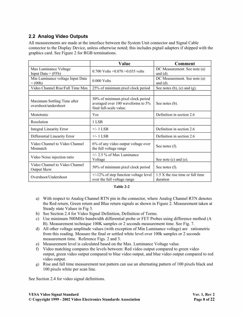
2.2 Analog Video Outputs All measurements are made at the interface between the System Unit connector and Signal Cable connector to the Display Device, unless otherwise noted; this includes pigtail adapters if shipped with the graphics card. See Figure 2 for RGB terminations.
Value Comment Max Luminance Voltage Input Data = (FFh) 0.700 Volts +0.070 /-0.035 volts DC Measurement. See note (a)
and (d). Min Luminance voltage Input Data = (00h) 0.000 Volts DC Measurement. See note (a)
and (d). Video Channel Rise/Fall Time Max 25% of minimum pixel clock period See notes (b), (e) and (g).
Maximum Settling Time after overshoot/undershoot
30% of minimum pixel clock period averaged over 100 waveforms to 5% final full-scale value.
See notes (b).
Monotonic Yes Definition in section 2.6
Resolution 1 LSB
Integral Linearity Error +/- 1 LSB Definition in section 2.6
Differential Linearity Error +/- 1 LSB Definition in section 2.6
Video Channel to Video Channel Mismatch
6% of any video output voltage over the full voltage range See notes (f).
Video Noise injection ratio +/- 2.5 % of Max Luminance Voltage
See note (c) and (e).
Video Channel to Video Channel Output Skew 50% of minimum pixel clock period See notes (f).
Overshoot/Undershoot +/-12% of step function voltage level over the full voltage range
1.5 X the rise time or fall time duration
Table 2-2
a) With respect to Analog Channel RTN pin in the connector, where Analog Channel RTN denotes
the Red return, Green return and Blue return signals as shown in Figure 2. Measurement taken at Steady state Values in Fig 3.
b) See Section 2.4 for Video Signal Definition, Definition of Terms. c) Use minimum 500MHz bandwidth differential probe or FET Probes using difference method (A
B). Measurement technique 100K samples or 2 seconds measurement time. See Fig. 7. d) All other voltage amplitude values (with exception of Min Luminance voltage) are ratiometric
from this reading. Measure the final or settled white level over 100k samples or 2 seconds measurement time. Reference Figs. 2 and 3.
e) Measurement level is calculated based on the Max. Luminance Voltage value. f) Video matching compares the levels between: Red video output compared to green video
output, green video output compared to blue video output, and blue video output compared to red video output.
g) Rise and fall time measurement test pattern can use an alternating pattern of 100 pixels black and 100 pixels white per scan line.
See Section 2.4 for video signal definitions.
VESA Video Signal Standard Ver. 1, Rev 2 © Copyright 1999 - 2002 Video Electronics Standards Association Page 8 of 22
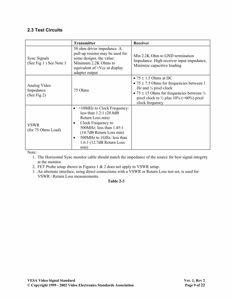
2.3 Test Circuits Transmitter Receiver
Sync Signals (See Fig 1 ) See Note 1
50 ohm driver impedance. A pull-up resistor may be used for some designs, the value: Minimum 2.2K Ohms to equivalent of +Vcc at display adapter output
Min 2.2K Ohm to GND termination Impedance. High receiver input impedance, Minimize capacitive loading
Analog Video Impedance (See Fig 2)
75 Ohms
• 75 ± 1.5 Ohms at DC • 75 ± 7.5 Ohms for frequencies between 1 Hz and ¼ pixel clock • 75 ± 15 Ohms for frequencies between ¼ pixel clock to ½ plus 10% (+60%) pixel clock frequency
VSWR (for 75 Ohms Load)
• <10MHz to Clock Frequency: less than 1.2:1 (20.8dB Return Loss min)
• Clock Frequency to 500MHz: less than 1.45:1 (14.7dB Return Loss min)
• 500MHz to 1GHz: less than 1.6:1 (12.7dB Return Loss min)
Note: 1. The Horizontal Sync monitor cable should match the impedance of the source for best signal integrity
at the monitor. 2. FET Probe setup shown in Figures 1 & 2 does not apply to VSWR setup. 3. An alternate interface, using direct connections with a VSWR or Return Loss test set, is used for
VSWR / Return Loss measurements. Table 2-3
VESA Video Signal Standard Ver. 1, Rev 2 © Copyright 1999 - 2002 Video Electronics Standards Association Page 9 of 22
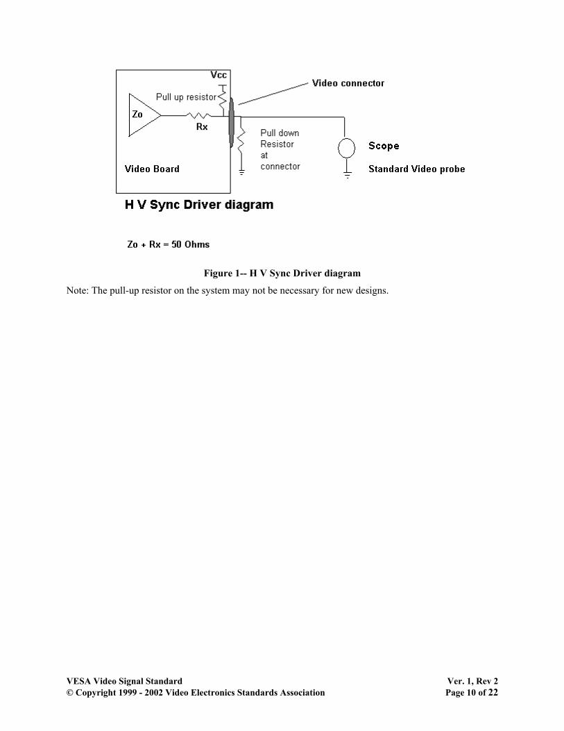
Figure 1-- H V Sync Driver diagram
Note: The pull-up resistor on the system may not be necessary for new designs.
VESA Video Signal Standard Ver. 1, Rev 2 © Copyright 1999 - 2002 Video Electronics Standards Association Page 10 of 22

Probes used are for example only. Equivalent probes and equipment may be used. An alternate interface, using direct connections with a VSWR or Return Loss test set, is used for VSWR/Return Loss measurements.
Figure 2 -- Video terminated measurement fixture
VESA Video Signal Standard Ver. 1, Rev 2 © Copyright 1999 - 2002 Video Electronics Standards Association Page 11 of 22
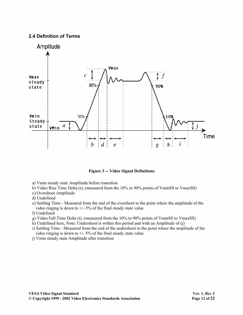
2.4 Definition of Terms
Figure 3 -- Video Signal Definitions
a) Vmin steady state Amplitude before transition b) Video Rise Time Delta (t), (measured from the 10% to 90% points of VminSS to VmaxSS) c) Overshoot Amplitude d) Undefined e) Settling Time - Measured from the end of the overshoot to the point where the amplitude of the video ringing is down to +/- 5% of the final steady state value f) Undefined g) Video Fall Time Delta (t), (measured from the 10% to 90% points of VminSS to VmaxSS) h) Undefined here, Note: Undershoot is within this period and with an Amplitude of (j) i) Settling Time - Measured from the end of the undershoot to the point where the amplitude of the video ringing is down to +/- 5% of the final steady state value j) Vmin steady state Amplitude after transition
VESA Video Signal Standard Ver. 1, Rev 2 © Copyright 1999 - 2002 Video Electronics Standards Association Page 12 of 22

2.5 Jitter Measurement Definition
Figure 4 -- Jitter Measurement Definition
Trigger scope at 1.5 volts on the rising or falling edge of the Hsync pulses. Measure the next Hsync pulse edge. The measured edge shall be the same polarity as the triggered edge. Accumulate the data for at least 100,000 edges. To derive the jitter measurement, subtract the minimum Hsync period from the maximum Hsync period and divide result by 2. A six sigma result uses all 100,000 samples to determine the total period deviation. For additional clarity see Fig 6.
2.6 Glossary of Terms LSB Least Significant Bit Monotonic 1. The property of either never increasing or never decreasing in reference to the slope of
a Transient response. 2. A constant slope value containing no inflection points. Sync Synchronization Signals TTL Transistor - Transistor Logic VSWR Voltage Standing Wave Ratio LSBc = (Vout (255)– Vout (0))/255
where Vout(255) is the voltage corresponding to the full scale output of an 8 bit DAC and Vout(0) is the zero level for the DAC. LSBc is the change in voltage corresponding to a one-LSB change in DAC value. Vout (255) is the maximum voltage present and Vout (0) is the minimum output voltage.
VESA Video Signal Standard Ver. 1, Rev 2 © Copyright 1999 - 2002 Video Electronics Standards Association Page 13 of 22

INL (Integral Linearity Error) = (V(n)-LSBc*n)/LSBc where V(n) is the DAC output voltage level measured at the nth step and LSBc*n is the ideal DAC level measured at the nth step. INL is thus the actual nth value compared to the ideal nth value and normalized to the ideal LSB.
DNL (Differential Linearity Error)= (V(n)-V(n-1))/LSBc
DNL is the difference between the DAC output voltage measured at the nth value and the previous n-1 value. DNL is normalized to the ideal LSB.
Overshoot/Undershoot Overshoot is defined as a positive going pulse during a transition time. Undershoot is defined as a negative going pulse during the transition time.
Pigtail
A short piece of cable with two connectors on each end for converting between one connector type and another. Common pig-tails are 9- to-25-pin serial-port converters and cables to connect PCMCIA network cards to an RJ-45 network cable.
2.7 References IBM Personal System/2 Hardware Interface Technical Reference - Common Interfaces, 84F9809 S84F-9809-00, pp 106-113. IBM Personal System/2 Hardware Interface Technical Reference - Common Interfaces, 84F9809 S84F-9809-00, pp 105. High Speed Digital Design (A Handbook of Black Magic), Johnson, H. and Graham, M., Prentice Hall, ISBN 0-13-395724-1, pp 108-110
VESA Video Signal Standard Ver. 1, Rev 2 © Copyright 1999 - 2002 Video Electronics Standards Association Page 14 of 22

3. Appendix A - Wave Form Diagrams
Vout low Steady
Vou
t Hig
h
Stea
dy st
ate
Vout min
Vou
t Max
Vpk
-pk
Vou
t hig
h M
inim
um v
alue
Figure 5 -- Pulse Definitions, general
VESA Video Signal Standard Ver. 1, Rev 2 © Copyright 1999 - 2002 Video Electronics Standards Association Page 15 of 22

Figure 6 -- Periodic Jitter (positive active pulse shown)
Period of Jitter
Min period
Max period
VESA Video Signal Standard Ver. 1, Rev 2 © Copyright 1999 - 2002 Video Electronics Standards Association Page 16 of 22

Signal
Voltage ripple and noise
Figure 7 -- Voltage Ripple and Noise
VESA Video Signal Standard Ver. 1, Rev 2 © Copyright 1999 - 2002 Video Electronics Standards Association Page 17 of 22

4. Appendix B – Suggestions for Tests ---VESA FPDM2 references---- Section 301-3A, page 34, Test Image references Section 303-9, Page 86, Waveform Analysis Section 305-6, pages 113-114, Jitter Section A112-2, pages 235-238, Setup Targets in FPDMSU Section A112-5, page 234, Patterns for Suite of Basic Measurements. Section A300, pages 303-315, Glossary, Definitions, etc.
============================= Video Bandwidth Measurement ============================= Video Bandwidth Method A: Direct signal injection method. – Non-powered Test--- Objective: To determine the frequency response of the analog video signal path. Note that the setup for this test is exactly the same as for the Crosstalk Method A test, so it may be used for both. Comment: The analog video signal path is considered to be from the output of the ADC (Analog to Digital Converter) to the output of the graphics card. For some applications, it may be preferred to measure the output at the end of the cable (properly terminated in 75 Ohms) over which the video is to be delivered to the monitor. Cautions:
Assure there is no power to applied the graphics card for this test. • •
• • • •
This injection method assumes that the ADC is significantly higher impedance than that of the signal source.
Equipment: Swept signal system, such as
Network Analyzer Spectrum Analyzer with Tracking Generator Swept Signal Generator (sinusoidal) with Oscilloscope Cable and probe of 75 Ohms with an injector connector to carry the swept signal to the injection point on the PCB (printed circuit board). If the signal source is 50 ohms, then a 50 Ohm to 75 Ohm impedance matching circuit must be used.
Procedure: With _no power applied to the board_, inject a swept signal at the source point of the video signal path. In most properly designed boards, this may be a 75 ohm source termination resistor at or near to the ADC video signal output. Signal Amplitude to be --See Note 1-- at the injection point.(Note 1: This level should be determined by the board design. For example, if the ADC output impedance is high and there are active devices, such as clamping diodes in the signal path, the signal level should be high, such as 0.7V. If the ADC output impedance is low and there is any danger of damaging it by injecting a voltage, then the signal should be as low as required to assure no damage to the active device.)
VESA Video Signal Standard Ver. 1, Rev 2 © Copyright 1999 - 2002 Video Electronics Standards Association Page 18 of 22
Frequency range to be from <1kHz to a at least 2.5 times the pixel clock frequency, although a minimum upper frequency range of 500MHz is recommended. Flatter and higher frequency responses will require even higher upper frequency ranges. Measure the signal level at the output of the PCB (or end of an additional terminated video cable, if desired) of the swept signal. A complete set of video bandwidth measurements will include 3 measurements, one each for the Red, Green, and Blue channels. Data: A swept frequency response curve should be shown on the sweep measurement display which will deviate from an ideal response curve by no more than the specification. Specification:
Video Bandwidth: * -3dB point: PixClk minimum (-6dB or 50% attenuation if referenced to Voltage) * -2dB point: 0.85*PixClk minimum (-4dB or 0.63 of original level if referenced to Voltage) * Flatness: +/- 1.2dB maximum to 0.8*PixClk
Analysis: A quality video signal path will produce a flat frequency plot, and will be attenuated no more than 3dB (6dB if referenced to voltage) at a frequency equal to the clock frequency. If video frequency response is not flat in the pass band and does roll off at too low a frequency, a number of video artifacts will occur, including loss of high spatial frequency details and nonlinear luminance degradation. Note that often for EMI considerations, circuit elements are placed in the video path that will attenuate the video level. Ideal video would have no such elements and would have no rolloff. This test will help determine if EMI components in the video path degrade the video quality level. -------------------------------------------------------- Video Bandwidth Method B: Generated signal method. This is an alternative or complimentary method to the direct signal injection method, and tests the entire graphics signal generation system actively. This requires special test signals to be provided in a future version of the FPDM measurement test suit and will be deferred in this standard until a future revision. ============ Crosstalk ============ Crosstalk Method A: Direct signal injection method bandwidth method. --Nonpowered Test--- Note that this setup is exactly the same as for the Video Bandwidth measurement, method A. The only difference is that the output is not the channel which has a signal injected, but a neighbor channel. Objective: Determine the frequency dependent crosstalk of the analog video signal path Comment: The analog video signal path is considered to be from the output of the ADC (Analog to Digital Converter) to the output of the graphics card. For some applications, it may be preferred to measure the output at the end of the cable (properly terminated in 75 Ohms) over which the video is to be delivered to the monitor.
VESA Video Signal Standard Ver. 1, Rev 2 © Copyright 1999 - 2002 Video Electronics Standards Association Page 19 of 22

Cautions: Assure there is no power to applied the graphics card for this test. •
•
• • • •
This injection method assumes that the ADC is significantly higher impedance than that of the source
Equipment: Swept signal system, such as
Network Analyzer Spectrum Analyzer with Tracking Generator Swept Signal Generator (sinusoidal) with Oscilloscope Cable and probe of 75 Ohms with an injector connector to carry the swept signal to the injection point on the PCB (printed circuit board). If the signal source is 50 Ohms, then a 50 Ohm to 75 Ohm impedance matching circuit must be used.
Procedure: With _no power applied to the board_, inject a swept signal at the source point of the video signal path. In most properly designed boards, this may be a 75 Ohm source termination resistor at or near to the ADC video signal output. Signal Amplitude to be --See Note 1-- at the injection point. (Note 1: This level should be determined by the board design. For example, if the ADC output impedance is high and there are active devices, such as clamping diodes in the signal path, the signal level should be high, such as 0.7V. If the ADC output impedance is low and there is any danger of damaging it by injecting a voltage, then the signal should be as low as require to assure no damage to the active device.) Frequency range to be from <1kHz to a at least 2.5 times the pixel clock frequency, although a minimum upper frequency range of 500MHz is recommended. Flatter and higher frequency responses will require even higher upper frequency ranges to examine crosstalk characteristics. Measure the signal level at the output video connector of the PCB (or end of an additional terminated video cable, if desired) of the video channels other than that of the swept signal. For example, if the signal is injected into the Red channel, the measured output will be either on the Green or Blue channels A complete set of crosstalk measurements will include 6 measurements, as per the following table.
Case Injection PointRed Green Blue
1 Red --- Yes Yes2 Green Yes --- Yes3 Blue Yes Yes ---
Measured Outputs
Data: Crosstalk is the amount of signal energy that couples into adjacent signal paths. For the ideal case, there is perfect isolation, and none of the signal energy would couple to the other channels. In the practical case, parasitic reactive components will allow for a lower impedance path for the signal to couple to the other channels as the frequency goes up. When looking at an adjacent video channel, a swept response curve that increases in amplitude as the frequency goes up will be seen. This can cause numerous problems to be seen in the video, including peaking, shadowing, smearing, color distortions, and a general level of distorted video, especially for higher spatial frequency component video, such as for many text characters or other fine detail.
VESA Video Signal Standard Ver. 1, Rev 2 © Copyright 1999 - 2002 Video Electronics Standards Association Page 20 of 22

Specification: Crosstalk (for input on any RGB video channel measured at the output of any other channel)
* -22dB or more to 0.85*PixClk * -18dB or more to PixClk * -10dB or more to 500MHz
Analysis: A good design with enough interchannel isolation will produce minimal cross-channel coupling, or crosstalk. The crosstalk level should have no level higher by no more than the specification. ------------------------------------------ Crosstalk Method B: Generated signal method. This is an alternative or complimentary method to the direct signal injection method, and tests the entire graphics signal generation system actively. This requires special test signals to be provided in a future version of the FPDM measurement test suite and will be deferred in this test until a future revision. ====================== Jitter (Video Signal) ====================== Objective: Determine the level of p-p jitter on the video signal. Comments: For the optimal case, jitter is measured in reference to a very stable frequency source, such as precision laboratory references. To measure jitter on the video signal, the reference would have to be phase-locked to the clock generator of the graphics card, or used directly as the board's clock. It is the user's discretion to use the most precise method of measuring jitter. Within this specification, a simpler, more direct approach is used which will approximate the true jitter of the video signal. It references the video jitter to the horizontal sync. While the sync and video are generated from the same source originally, and therefore are intrinsically frequency-locked, the electrical and visual characteristics from sync signal are dramatically different from those of the video, both on a graphics card and in cables. On graphics cards, issues such as differing ground planes, uncontrolled impedance traces, non-ideal signal routing and active signal processing devices can introduce temporal artifacts to the video and sync independently. The differential in jitter between sync and video can produce unstable video at the pixel level, which is often clearly visible on CRT's and can produce dynamic clock and phase generation errors on LCD's. Equipment: Digitizing oscilloscope, with probes for both of the video channels to be tested and for horizontal sync. A sync separator may be needed for the case of composite sync. Procedure:
Use an all white pattern for testing • • •
•
Trigger on the Hsync signal View the video channel, centering the trace and expanding the vertical gain to be at or near maximum. Use 100,000 samples and six sigma statistical analysis to determine the p-p temporal excursions.
VESA Video Signal Standard Ver. 1, Rev 2 © Copyright 1999 - 2002 Video Electronics Standards Association Page 21 of 22
VESA Video Signal Standard Ver. 1, Rev 2 © Copyright 1999 - 2002 Video Electronics Standards Association Page 22 of 22
• Specification:
P-P jitter shall be less than 1/5 PixClk and less than 2 times the rise time to insure suitable video integrity.
Analysis: One future consideration is to add an integrator to the sync signal in the measurement path, to decrease any effects of its jitter on the jitter of the video signal. Note that there are alternate ways to measure jitter on a CRT display using fast optical detector devices, and those types of measurements may be used as supplements to this measurement. Reference FPDM2 Section 305-6, pages 113-114, Jitter. ==================================== Video Signal-to-Noise Measurement ==================================== Note: This test can only be done for a graphics card, which is powered on, and uses special test signals that are under development for the FPDM measurement test suite. Therefore, it will be deferred in this standard until a future revision of FPDM.