analysis, simulation and modeling of three-level vsis …
TRANSCRIPT

ANALYSIS, SIMULATION AND MODELING
OF THREE-LEVEL VSIs
by Muhammet Cosan
A thesis submitted to the Faculty of the
Virginia Polytechnic Institute and State University
in partial fulfillment of the requirements for the degree of
MASTER OF SCIENCE
in
Electrical Engineering
a Co Approved by: ere fer C
Dr. Dusan Bérojevic, Chairman
fice { C : yoru “a 2S oS a Dr. Fred C. Lee | ““e* “Dr, Jason Lai
—— a .
November 1997
Blacksburg, Virginia

ANALYSIS, SIMULATION AND MODELING OF
THREE-LEVEL VSlIs
by
Muhammet Cosan
Dusan Borojevic, Chairman
Electrical Engineering
(ABSTARCT)
Analysis of three-phase, three-level VSIs is done for high-
power high-voltage applications. Complete Space Vector Modulation
(SVM) algorithm is developed for a three-phase, three-level converter.
Special attention is given to minimization of output ripple and voltage
balance of the dc-link input capacitors. Verification of the proposed SVM
algorithm is done by computer simulation. Comprehensive small-signal
modeling of the three-level converter with a resistive load is developed the
first time. Steady-state solutions reveal that the voltage across dc-link
input capacitors is constant at the half of the dc-link voltage.
Acknowledgments
| would like to thank my advisor, Dusan Borojevic, for his invaluable
support, understanding and encouragement. This work would not be possible
without his esteemed guidance. | am also thankful to him for providing me with
the opportunity to work at the Virginia Power Electronics Center (VPEC). Itis a
pleasure and an honor to be a VPEC graduate.
A great deal of credit for this work goes to my colleague Dr. Hengchun
Mao. | would like to express my sincere gratitude to him for his help in this
course of work. | also would like to thank Dr. Eng. Josep Bordonau, visiting
scholar of Universitat Politecnica De Catalunya, Barcelona, Spain, for his
valuable discussions and inputs especially in the modeling of the converters.
| am also grateful to Dr. Fred Lee, Dr. Dan Y. Chen, and Dr. Jason Lai
whose teaching gave me a head start and a better understanding of power
electronics. The completion of this thesis would not be possible without the
valuable help given by friends Dong-Ho Lee and Heping Dai.
| am also thankful to all the departmental staff, and especially VPEC staff
for their help during the course of this work. | am also grateful to Westinghouse
Electric Co., for supporting this work.
iil
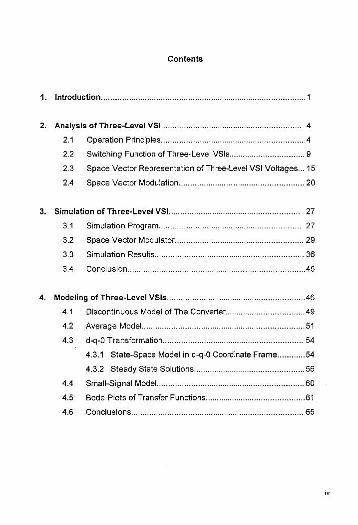
Contents
IMtrOCUCTION....0.. 2... ccceccccceececaeeeeccneeceeceeeeeeeeeeeecensceeaeseaeeseereeeesaes 1
Analysis of Three-Level VSI................ cece ceseesececeneecneesaeceececeeceeees 4
2.1 Operation Principles... cccccssssssssssssseeeeeneneceseeeeeneenecees 4
2.2 Switching Function of Three-Level VSI... eeeeeeeeeeee ees 9
2.3. Space Vector Representation of Three-Level VSI Voltages... 15
2.4 Space Vector Modulation.............. cece ccccecceeececeseeeceeeeceeeeens 20
Simulation of Three-Level VSI... ceeeeseceeeeeeneeeeeeeeeenenes 27
3.1 SIMU ATION PrOgraM.......... ce eeccccsessesseneeceeeseuenaneeeeeeeeeeeeneeeees 27
3.2 Space Vector Modulator..............eceessesccceccceeceeneeeeseeseeeaeeeens 29
3.3 Simulation ReSults........... eee eeesceeeeeeeeenceeecenaeeeeeeeeeeeeaeaes 36
3.4 CONCIUSION Le. eccccccc cee eeeeeeeneaueaeensaneeeeeeenecaueserenaeeseeeeesaees 45
Modeling of Three-Level VSIS.................ccccceseeeeeenecentteeeeeeeeeeceeeeeeeseeses 46
4.1. Discontinuous Model of The Converter.............. ce ceeeeeeeeeeee eee 49
42 Average Model... ccesecceccencececeeeesereecseeeteeeseeeeseeeeeeaesees 51
4.3 d-q-O Transformation. .............ccccccccccssecesseessseeseseseeeeeesecanseceeees 54
| 4.3.1 State-Space Model in d-q-0 Coordinate Frame............ 54
4.3.2 Steady State SolUtions......... ee eeeeccsseeeeeneeseseeeers 56
44 Small-Signal Model............ cc cccccccccssessssesseeeeeeeececesseaseeeees 60
4.5 Bode Plots of Transfer FUNCTIONS... eee eeeeeeeeeeeeeeeeeeees 61
4.6 CONCIUSIONS...00.... eee ecc cc ecseccceeceeceneeeeeceeseeeseeeeeceseneeeeeeaeeeees 65

5. Summary and Future Work...................0ccccccceeessecceccesessseeeeceaeeseenestenees 66
Appendix A Sequence of The Vectors for Each Sector................0........ 68
Appendix B Duty Cycle Calculations......0..000.0 ence eeeee eee eeees 70
Appendix C Saber Netlist of Three-Level VSI..0..... eee eeeeeeeees 78
Appendix D Complete SVM Algorithm.............0... ee ereeeeeeeeeeeeeeees 80
Appendix E Transfer Functions. .........0....... ccc cecsccsssseeeeeeeeeeeeeeceeeeeeeeeeees 85
Appendix F Simulation of d-q-0 Model by PSPICE ....... ee. 87
REfFErENCES.......... cece cc ceccccesesecceececenneaeececaceeceaseececesaaeceecesecuaeeeeesenaeeeeaeeeeeeeeeees 90

Fig.
Fig.
Fig.
Fig.
Fig.
Fig.
Fig.
Fig.
Fig.
Fig.
Fig.
Fig.
Fig.
Fig.
Fig.
Fig.
Fig.
Fig.
Fig.
Fig.
Fig.
Fig.
1.2
2.1
2.2
2.3
2.4
2.5
2.6
2.7
2.8
2.9
2.10
2.11
3.1
3.2
3.3
3.4
3.5
3.6
3.7
3.8
3.9
List of Figures
Block diagram of a Superconductive Magnetic Energy
Storage (SMES) system and three-level VSI....................... 2
Power stage of a three-level VSI... ceecececseee ee eeeeees 3
An example of switching states of a three-level VSI. Thick
lines represent the active current path........0..... eee eee OD
Line-to-line voltages of two-level vs three-level VSls.............. 8
A two-level VSI leg represented as two switches........0.0.000000. 10
Single-pole-double-throw switch representation of
A TWO-lEVE! VSI. cece cece eee e ee ee ee eeeceeneaeenaeeaeeeaeeenes 11
A three-level VSI leg represented as three switches.............. 12
Switching function representation of three-level VSI.............. 13
Representing switching states poo and onn in space
VECO“ FOTN... 0. cece cece cee cee eee ee ee ene eee cee eee eee eeeteneeenaneneees 17
Space vector representation of three-level VSI line voltages..19
One of the sixty degree interval in Fig. 2.8.................cccceee eens 21
Sequence of the vectors in One CYCIE....... ee ececcceeseeeeeeeeeees 24
Synthesis of the reference vector “V" ow... cccccecccceeee serene 25
Block diagram of the SABER simulation..................ccccccceeeee 28
Finding the da and df projections... eceeeeeeeneeeeees 30
FINGING de... ce ccc cc cece cece eee e cnet estes eee eeessecsenaeteaaeeeenaes 33
Each small equelateral triangle is represented by i,j
COMDINATIONS........ eee eeeeceecceeteeeeeeeceeeeeeeeteeeeeteeteteeeesees OO
Circuit parameters for Saber simulation.................ccccecceeseeesees 37
Output line Currents, ia, 1b, ic ....ccceccceeccccccessececeesceeeceescaseeneees 38
Output line currents in a sixty degree interval........................ 39
Output line-to-line voltages, vab, vAB, vBC, ANd VCA............06. 40
Midpoint Voltage, -v11...... ccc ccceeccecccesccceeesssceceeeeeeeuesecseeeceneenenes 41
Vi
Fig
Fig
Fig.
Fig.
Fig.
Fig.
Fig
Fig
. 3.10
. 3.11
4.1
4.2
4.3
4.4
. 4.5(a)
. 4.5(b)
Harmonic content of output Current, ia... cece ceeeseeeeees 43
Harmonic content of output Currents, ia......... cc eececccseeeeeeeee eee 44
Steps of obtaining the small-signal model of a three-phase
CONMVETIOT.......... cc. ccc ccc ccc ccc cecccecucccceneceeucecccccucesteecccuceececs 48
Switching function representation of three-phase
three-level VSI... ccc ec ee cece ceee tence cee eesateaee sae aeeaees 50
Average circuit model of a three-phase three-level VSI......... 53
Average circuit model in d-q-O0 coordinates.................c..cccecee 59
Frequency response of iYy/, eee eeececeeeeecsseceseeecauseeeeeaeseeceeeees 63 dpd
Frequency response of i t4/, soe ceaeeceeceeeeeeaeasseeseeaueeeeeeeeaecnaess 64 dpq
Vil

Table 1
Table 2
Table 3
Table 4
Table 5
Table 6
List of Tables
The relationship between level of a multi-level converter
and number of switches, switching combinations,
admissible states and free wheeling states...................
Switching states in a three-level VSI and
COrMeSPONMINgG OUtPUIS............. cece cece eect ee ences cen enneeees
The sequence of the switching vectors in first sixty
degree interval ............ ccc ccc cece e cece cee cceeeenee nse eee een ene eens
Steady state SOIUTIONS............ ec eecccccececceceseesaeseecsaeeaseceeeees
Steady state solutions for input Side... cece eeee neers
Operating point values for small-signal analysis....................
Viil
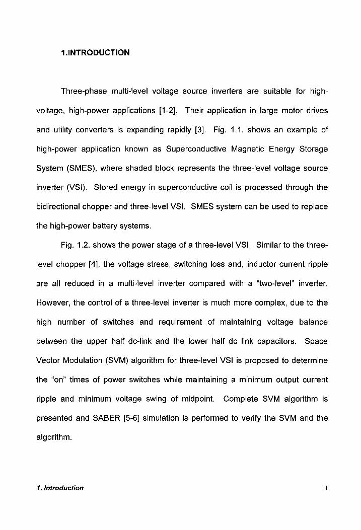
1.INTRODUCTION
Three-phase multi-level voltage source inverters are suitable for high-
voltage, high-power applications [1-2]. Their application in large motor drives
and utility converters is expanding rapidly [3]. Fig. 1.1. shows an example of
high-power application known as Superconductive Magnetic Energy Storage
System (SMES), where shaded block represents the three-level voltage source
inverter (VSI). Stored energy in superconductive coil is processed through the
bidirectional chopper and three-level VSI. SMES system can be used to replace
the high-power battery systems.
Fig. 1.2. shows the power stage of a three-level VSI. Similar to the three-
level chopper [4], the voltage stress, switching loss and, inductor current ripple
are all reduced in a multi-level inverter compared with a “two-level” inverter.
However, the control of a three-level inverter is much more complex, due to the
high number of switches and requirement of maintaining voltage balance
between the upper half dc-link and the lower half dc link capacitors. Space
Vector Modulation (SVM) algorithm for three-level VSI is proposed to determine
the “on” times of power switches while maintaining a minimum output current
ripple and minimum voltage swing of midpoint. Complete SVM algorithm is
presented and SABER [5-6] simulation is performed to verify the SVM and the
algorithm.
1. Introduction 1
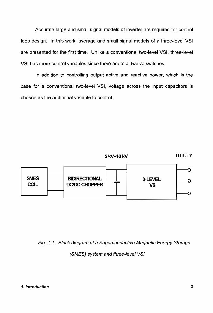
Accurate large and small signal models of inverter are required for control
loop design. In this work, average and small signal models of a three-level VSI
are presented for the first time. Unlike a conventional two-level VSI, three-level
VSI has more control variables since there are total twelve switches.
In addition to controlling output active and reactive power, which is the
case for a conventional two-level VSI, voltage across the input capacitors is
chosen as the additional variable to control.
2 kV~10 kV UTILITY
SMES BIDIRECTIONAL 3-LEVEL COIL DC/DC CHOPPER VSI
L
Fig. 1.1. Block diagram of a Superconductive Magnetic Energy Storage
(SMES) system and three-level VS!
1. Introduction 2

C1
Yn =
C2
$1 $3 S5
Sz S aa\ S6\ La
| | LIVf_
Su | S3 S55
a>
S2 S4 S6é | |
1. Introduction
Fig. 1.2. Power stage of a three-level VS!

2. ANALYSIS OF THREE-LEVEL VSis
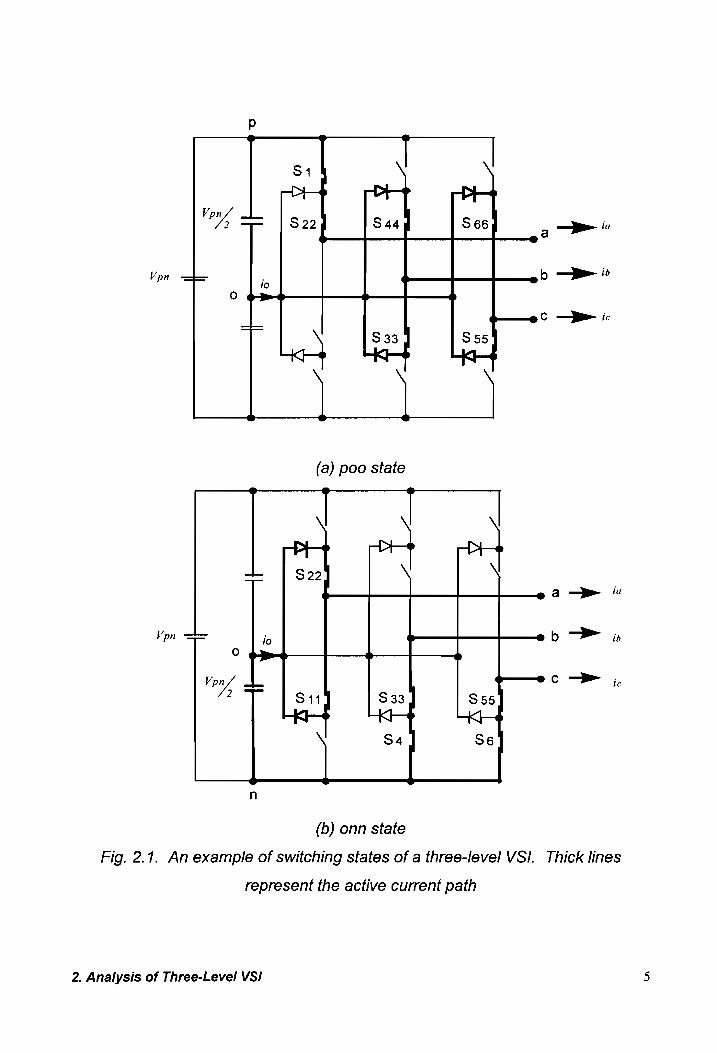
2.1. Operation Principles
Each phase leg of the three-level VSI shown in Fig. 1.2 is composed of
two upper and lower switches and their antiparallel diodes. Two input capacitors
split the dc-bus voltage into two halves. In addition, six clamping diodes ensure
that voltages across the switches will be determined by the voltages of the = dc-
link capacitors. The charge balance of the midpoint can be achieved by using a
proper modulation scheme. Switching states for a three-level VSI must satisfy
the following conditions:
e no shorting of the input capacitors, and
e continuity of the inductor current.
Fig. 2.1 (a) and (b) shows the two switching combinations of a three-level
VSI. Notation “p’, “o”, and “n” means corresponding phase is connected to the
positive rail, midpoint, and the negative rail, respectively. Note that, in addition to
M33
p” and “n” states of the conventional two-level VSI, in three-level VSI a phase
can be connected to the midpoint, “o” state. In Fig. 2.1 (a), line-to-line voltages
are v., = lm Vio = 91 Vea = beng and i, =—i,. On the other hand, in
Fig. 2.1 (b), v,, ae =0, Veg =P, and i, =i,. This kind of
switching combinations produce the same output voltage but utilize the different
dc-link capacitors and can be used for charge balance of the input capacitors.
Bidirectional power flow in a three-level VSI can be achieved by
controlling the 12 switches. For a converter with 12 power switches, there are
total 12? switching states. However, only 27 states satisfy the above conditions,
and the rest of the states either short the input capacitors or open the output
current path. Table 1 shows the relationship between the number of the
switches, number of admissible switching combinations, number of free-wheeling
states, so called zero vectors, and the level of the converter.
2. Analysis of Three-Level VS/ 4
Vpn
Vpn
|
¢—_~.
n
(b) onn state
represent the active current path
2. Analysis of Three-Level VSI
| | S4 a |
Vpn °/. A= | S22 S44 S66 3
oe
— io ? ob >" 0 @o>e | >
Cc —P- ic
TS \ at S55
oe } | )
(a) poo state
ro] |
=“ S22 \ \
oa «4
L—— io e ob > |
0 rt 4 Vpn co > .
Vf $11 S 33 S55
S4 S6
Fig. 2.1. An example of switching states of a three-level VSI. Thick lines

Table 1 The relationship between level of a multi-level converter and number of
switches, switching combinations, admissible states and free-wheeling states
Number of Number of Number of Num. of Free
Switches Switching Admissible Wheeling
Combinations | Switching States States
2-level 6 6? 8 2
3-level 12 12? 27 3
4-level 18 18? 64 4
m-level | n=(m-1)-6 n? m? m
2. Analysis of Three-Level VS! 6
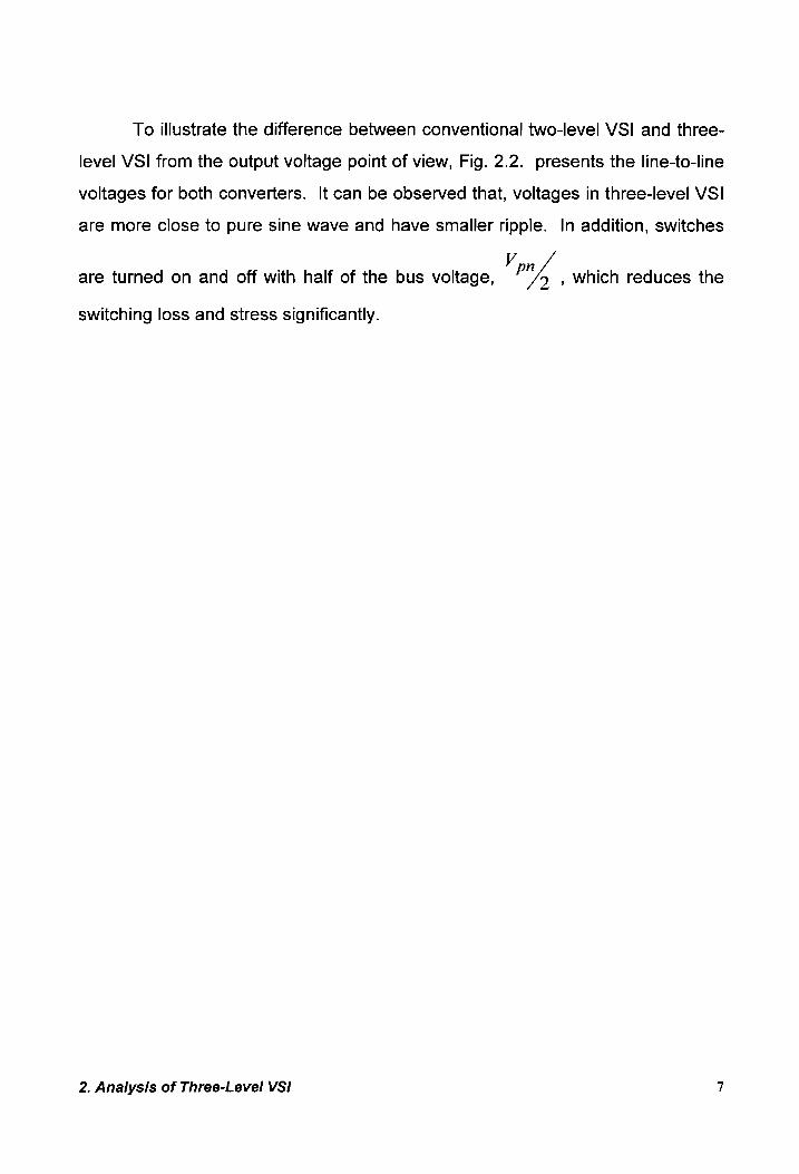
To illustrate the difference between conventional two-level VSI and three-
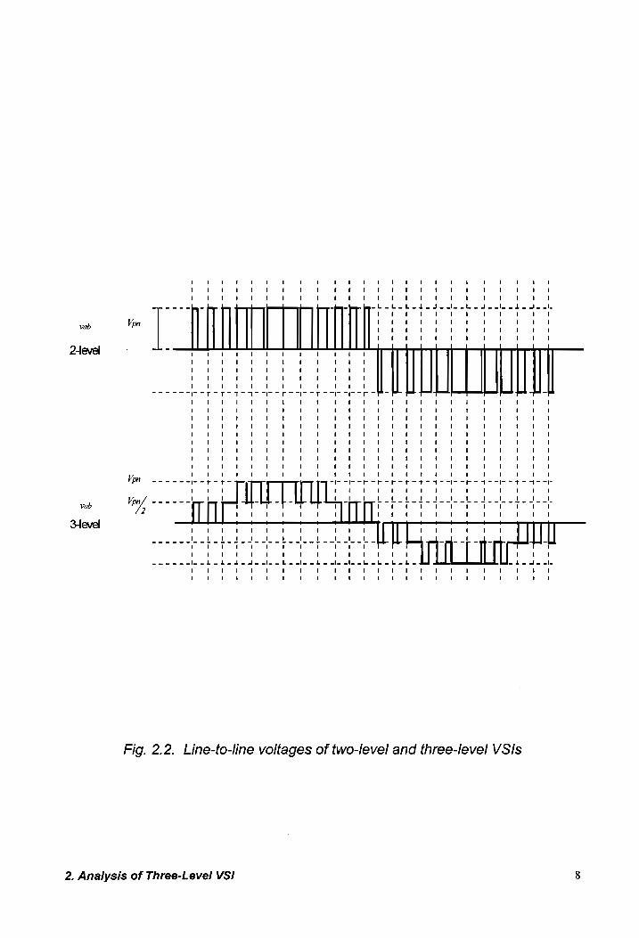
level VSI from the output voltage point of view, Fig. 2.2. presents the line-to-line
voltages for both converters. It can be observed that, voltages in three-level VSI
are more close to pure sine wave and have smaller ripple. In addition, switches
V. are turned on and off with half of the bus voltage, pn which reduces the
switching loss and stress significantly.
2. Analysis of Three-Level VS/ 7
-
--- eee
ed Po
- ------
- pee
-i--
a
,_ . +--+ --
a
on
~o-4e---d Poo eee
tee -
4.
ov ;
a
| Los
i )
TST TT
SSS
SS SS SSP
TTT TO
77
>
' '
' 1
---4-----—=
---------- r--a--f--
-- 3
_ooge eee Pd
ee Loud
de 3
1! t
' t
——
t l
' '
1
TT Ty
TT
TTT
eS SSE TST
77
®o
---4---- fd
eee Cot
a.
© ---4----,_
I] ___
ee tenead-
_- s
~ou4--__4 ood
_ ee
tea pe
Loe
g _--4--ee —j_ re
Leow.
fe ie.
6
~oo4 ~---4 ———F
wee
ee eee Lute
get
ee
oO 1
v t
, 1
' Ss
_ ee
L~--------- 1--D
a.
o '
v~T ._---—.----
Lo o-------- 8 -
ese g
eet
oe eee
ee ee LL
UL Lg Le
=
oo |
_
rot “
---E----- ba nannnn ane pod
5 '
‘ 1
eel eee
ee
~w~- fee
e- eee
®
, ot
=) Tope pT
opr
x --->—-- ---
t~---------
--}--|--4-- Q
1 1‘
t J
>
-----
aatietiatietiatietetetetel --grcuc
can: ®
' i
t c
2s a
———=]---
- - rote coco
oo
~~ Frome rAd
=
__._o____. Lote ps
o -_—
,- ee
} eee
pT
, 77 Po
2 ---——-----
Poo --
2-22 be
ia-
5 l
' '
i i
i
t '
t t
a t
a
‘ 1
' '
’ '
' N
t-—_
\ tot
roa AN
~ &
a ss
2
vab
2-level
vab
level
2. Analysis of Three-Level VS/
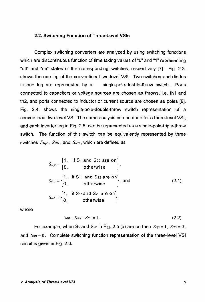
2.2. Switching Function of Three-Level VSIs
Complex switching converters are analyzed by using switching functions
which are discontinuous function of time taking values of “O” and “1” representing
“off and “on” states of the corresponding switches, respectively [7]. Fig. 2.3.
shows the one leg of the conventional two-level VSI. Two switches and diodes
in one leg are represented by a single-pole-double-throw switch. Ports
connected to capacitors or voltage sources are chosen as throws, i.e. tht and
th2, and ports connected to inductor or current source are chosen as poles [8].
Fig. 2.4. shows the single-pole-double-throw switch representation of a
conventional two-level VSI. The same analysis can be done for a three-level VSI,
and each inverter leg in Fig. 2.5. can be represented as a single-pole-triple-throw
switch. The function of this switch can be equivalently represented by three
switches Sap, Sao, and San, which are defined as
{0 if Si and S22 are on ap =
0, otherwise
5 1, if S11 and S22 are on q 34
7°10, otherwise yan (2.1)
1, if Si1and S2 are on San = . ;
O, otherwise
where
Sap + Sao + San = 1. (2.2)
For example, when Si and $22 in Fig. 2.5.(a) are on then Sap=1, Sao=0,
and San=0. Complete switching function representation of the three-level VSI
circuit is given in Fig. 2.6.
2. Analysis of Three-Level VS/ 9

S1 ia
—_>
Vpn
S2 \
n
(a) One leg
p
th1
Sap la
— pole
Vp. oo
San
th2
n
(b) Switching function representation of one leg
Fig. 2.3. A two-level VSI leg represented as two switches.
2. Analysis of Three-Level VS! 10

ln ——
Fig. 2.4. Single-pole-double-throw switch representation of a two-level VSI
2. Analysis of Three-Level VS! 11

Van =S=="
(a) One leg
p
C1
th2 o @———0
Sao
C2
n
th
la
Sap —>pP>
pole
San
th3
(b) ) Switching function representation
Fig. 2.5. A three-level VSI leg represented as three switches.
2. Analysis of Three-Level VSI 12

1] I] > = oO :
tA
3 wn Ss Oo
- Sen
$ TT I
Fig. 2.6. Switching function representation of three-level VSI.
2. Analysis of Three-Level VSI 13

From Fig. 2.6., output line-to-midpoint voltages (vao,vbo,vco) can be
written in terms of input voltages (vp, vn), and input currents (ip,in) can be
written in terms of output line currents (ia ib, ic) by using switching functions.
input/output current and voltage relations of the circuit given in Fig. 2.6. can be
completely defined as
vao Sap San
vbo |=| Sbp Sbn |- vn =[S]-[vg] 3)
Vco Scp Sen
and
; la P| r |,
in| | LS] aan (2.4) Le
For example, when the poo switching state is applied, above matrix equations
can be written as
vao 1 0 y P
vbo|=|0 0 vn | , (2.5)
vco 0 0
and
ip es ee in| |0 0 0 (2.6)
L.
Note that, midpoint current is
lo = —Ip —in. (2.7)
2. Analysis of Three-Level VS! 14

2.3 Space Vector Representation of Three-Level VSI Voltages
Space vector representation is a very useful and common method of
analyzing three-phase converter circuits [9]. As an example, switching states
poo and onn can be shown in a complex plane as in Fig. 2.7., so that the
projections of vector V01 on line-to-line voltage axes are yas = YPM, , vea=0, and
vea =~ Ven This requires the magnitude of vector V01 to be PY 3 and the angle
to be 0°. Switching states shown in Table 2 have magnitude and phase
information that can be expressed in terms of voltage space vectors as in Fig.
2.8. The switching vectors of the three-level VSI can be divided into four groups
according to their magnitudes: zero vectors, small vectors, V01, ..., Voé , medium
vectors, V12, ...V61, and large vectors, V1, ..., Vé. Different switching vectors
have different effects on the charge balance of the midpoint, output ripple, and
switching loss. Each small vector represents two different switching
combination, positive and negative. For example, vector Vo1 when it is obtained
from the combinations poo is called a positive-combination-vector (V01p), and
when it is obtained from noo, it is called negative-combination-vector (V01n).
Both vectors produce the same output voltage, but when the positive vectors are
applied, the upper capacitor is charged or discharged, and when the negative
vectors are applied, the lower capacitor is charged or discharged. This property
of the small vectors provides the freedom which can be used to control the
charge balance of the dc-link midpoint. Combinations that produce medium
vectors also affect the midpoint voltage, but there is only one combination for
each vector. Lastly, large vectors and zero vectors do not change the voltage of
the midpoint. In terms of line-to-line voltages, the magnitude of the large vectors
is or on and the magnitude of small vectors is ”?” ;- The magnitude of the
medium vector is equal to /pn , which is the same as the maximum radius of a
2. Analysis of Three-Level VS! 15

circle that can be inscribed into the large hexagon in Fig. 2.8. Therefore, the
maximum amplitude of undistorted output line voltage is Vpn.
The desired output line voltage vector in steady-state can be represented
as:
V(O) = Dmod -Vpn- ef) | 6=a-t (2.8)
where 0<|V|<Vpn is the output line voltage, 0< Dmod<1 is the modulation
index, and @ is the frequency of the output voltage. From the modulation index
3 3 (Dmod ) a parameter dm is defined as dm= “5 Dmod, where 0<dm< 8
2. Analysis of Three-Level VSI 16

Vbc A
Vab
Fig. 2.7. Representing switching states poo and onn in space vector form.
2. Analysis of Three-Level VS! 17

Table 2 Switching states in a three-level VSI and corresponding outputs
Switching | Name of vab vbe vea io ip
states the vector
ppp Vo 0 0 0 0 0
nnn Vo 0 0 0 0 0
000 Vo 0 0 0 0 0
poo Vo1p Vpn/2 0 -Vpn/2 ib +ic ia onn Voin Vpn/2 0 -Vpn/2 ia 0 ppo Vo02p 0 Vpn/2 -Vpn/2 ic ia +ib
oon Vo02n 0 Vpn/2 -Vpn/2 ia+ib 0
opo Vo03p -Vpn/2 | Vpn/2 0 la tic ib non Vo3n -Vpn/2 Vpn/2 0 ib 0
opp V04p -Vpn/2 0 Vpn/2 ia ib+ic
noo Vo4n -Vpn/2 0 Vpn/2 ibtic 0
oop Vo5p 0 -Vpn/2 | Vpn/2 ia+ib ic
nno Vo5n 0 -Vpn/2 Vpn/2 ic 0
pop Vo06p Vpn/2 | -Vpn/2 0 ib ia +ic ono Vo6n Vpn/2 -Vpn/2 0 ia tic 0
pon V12 Vpn/2 Vpn/2 -Vpn ib ia
opn V23 -Vpn/2 Vpn -Vpn/2 0 ib
npo V34 -Vpn Vpn/2 Vpn/2 ic ib nop V45 -Vpn/2 | -Vpn/2 Vpn ib ic onp V56 Vpn/2 -Vpn Vpn/2 ia ic
pno Ve1 Vpn -Vpn/2_ | -Vpn/2 ic ia
pnn V1 Vpn 0 -Vpn 0 ia
ppn V2 0 Vpn -Vpn 9) ia +ib
npn V3 -Vpn Vpn 0 0 ib
npp V4 -Vpn 0 Vpn 0 ib+ic
nnp V5 0 -Vpn Vpn 0 ic
pnp Ve Vpn -Vpn 0 0 ia +ic
2. Analysis of Three-Level VS/ 18

Fig. 2.8. Space vector representation of three-level VS! line voltages.
2. Analysis of Three-Level VS/
19

2.4 Space Vector Modulation
The principle of SVM is to approximate the reference vector V in (2.8),
over one switching period, by using PWM of switching vectors in Fig. 2.8. The
task can be divided into two parts: first, selection of the switching vectors to be
used, and second, calculating the duty cycles of the selected vectors. Due to the
large number of switching vectors, there is a freedom in the choice of the vectors
and their duty cycles. This freedom can be used to optimize the following goals:
e minimum harmonics in the output waveforms,
¢ minimum midpoint current io,
e minimum number of switching actions (i.e. minimum switching losses).
The output voltage harmonics can be minimized (resulting in a small ripple
of the output current) if only the switching vectors nearest to the reference
vectors are selected for PWM. This is achieved by using adjacent switching
vectors located at the corners of the small triangle in which the reference vector
is located at a given instant. 24 small equilateral triangles within the hexagon
can be identified in Fig. 2.8., and the location of the reference vector can be
found from the geometry.
2. Analysis of Three-Level VS/ 20

V2
Re
Vv
Vo Vab
Fig. 2.9. One of the sixty degree intervals in Fig. 2.8.
2. Analysis of Three-Level VSI 21

Due to the circular symmetry, operation and duty cycle calculations can
be explained by using only one of the large triangles, Fig. 2.9. For the shaded
small triangle in Fig 2.9., the vector summation equations can be written as
V01-2,, + V02-t,, +V12-t,, =V-T.
(2.9)
toy thy +h, =T,,
where f,, fo), f;. and are the time duration of the vectors Vo1, Vo2, and V12,
respectively. Substituting
V01= - V02 = ee, V12= Vpn-e § , andV= Dmod-Vpn-e ©
and (2.8) into (2.9), fo, fo., and ty; can be solved as
ty) = T.(1- = dm-sin(6- 2)) = —_ —. -Sin _ 01 S V3 m 1 6 ;
= T, +g in(Q-—)-2-d 6-~)+1 d fon = Tgp dm sin(O —G)—2-dm-cos(O—G) +1), and 9
2 La a to= Ts yy am sin(@ — ) +2-dm-cos(@ ——-)— 1),
3 where dm = Dmoa-~2 . From (2.10.a), duty cycles for the vectors Vo1, Vo2, and
V12 can be defined as
t doi=—, doz=—, and d12=—. (2.10.b)
tw
w wy
In order to minimize the midpoint current, i.e. reduce the charge
unbalance of the input capacitors, positive and negative combinations of the
small switching vectors can be used alternately within each or alternate switching
cycles. An example of ordering the switching vectors is shown in Fig. 2.10. and
Fig. 2.11. In this example, oon and onn switching states utilize the lower dc-link
capacitor while poo switching state utilizes the upper dc-link capacitor. On the
2. Analysis of Three-Level VS! 22

other hand, pon switching state utilizes the upper and lower dc-link capacitors
but the ratio of the upper and lower dc-link capacitor currents depends on the
instantaneous value of the load current.
When V01 vector is split into two equal pieces, it has no effect on the
midpoint voltage. V02n and V12 vectors may have good or bad effects on the
midpoint voltage, depending on the instantaneous value of the load current,
which is not investigated in this work. The same way, V02 vector can be split into
two pieces as V02p and V02n in one switching cycle. In this case, Vo2 has no
effect on the midpoint voltage, but the effect of the Vo1n and V12 may be good or
bad, depending on the instantaneous value of the load current.
In Fig. 2.10, after Vo1p is applied, only one switching action is required to
apply the next vector V12 For the next switching cycle, the reverse order of the
above shown vectors can be applied to minimize the switching action and output
ripple. Table 3 shows the order of the vectors to apply for the big triangle in
Fig. 2.9.
Duty cycle calculations for other triangles can be done in a similar way for
other small triangles in Fig. 2.9. Appendixes A and B show the sequence of the
vectors used in every triangle and duty cycle calculations.
2. Analysis of Three-Level VS! 23

poo pon oon onn
Vo1p | Vi2 Vo2n Voin
<a Loy 4 thy Hh
ad
Fig. 2.10. Sequence of the vectors in one cycle.
For the next switching cycle, above vectors are applied in reverse order.
2. Analysis of Three-Level VS/ 24

V2
Vo2n d0in- VO1n nS Vi2
Fig. 2.11. Synthesis of the reference vector “v”
2. Analysis of Three-Level VS/
> Vi
25

Table 3 The sequence of the switching vectors in first sixty degree interval
Index of the triangles in Fig 2.9. Vector sequence
j=1 Vo1p, Vo, Vo2n, Voin
j=2 Voip, V12, V1, Voin
j=3 Vo01p, V12, V02n, Voin
j=4 Vo2p, V2, V12, Vo2n
2. Analysis of Three-Level VS! 26

3. SIMULATION OF THREE-LEVEL VSlis
3.1. Simulation Program
In many industry applications, prior to building large electrical and
electromechanical systems, a simplified model is developed and investigated by
simulation. It provides better understanding of the system and allows to evaluate
different control algorithms easily. This process reduces the time and money
needed to develop the prototype of the converter.
A SABER simulation program is developed for time domain simulation of
three-level three-phase inverter system. SABER is a powerful and widely used
simulation program introduced by Analogy Inc.
Fig. 3.1. shows the block diagram of the simulation circuit. There are two
input files, one is the main file to create netlist which is for the three-level VSI.
The second file is the SVM file and it performs the SVM algorithm to drive the
switches in main file.
Main file is the netlist of the power stage and is relatively strait forward.
As simulation time is swept from zero to desired value, main file runs the SVM
file to find the duty cycles and to derive the switches. Switches in power circuit
are considered as ideal to make the simulation simple. Resistors are used as
three phase load. For a nonresistive load, the phase between the voltage and
current should be taken into account in the SVM algorithm.
SVM file is a text file written in MAST which is the modeling language for
the Saber simulator. All electrical and electromechanical device models in Saber
library are written in MAST language. These files are called “templates”. MAST
models all elements by their characteristic equations. Saber provides the library
for commonly used components. However, there is no Space Vector Modulation
template in Saber. That is why, developing a MAST file to implement the SVM
algorithm for three-phase three-level VSI is a requirement for time domain
simulation.
3. Simulation of Three-Level VSIs 27

28
«—— T,, switching period
ratio
<—— /,,, transition time
<— x,midpoint balancing
LH
S4e S5e S6 |
sin(@ -f)
Dmod
A
Dinod
dm
| cos(@-t)
Fig. 3.1. Block diagram of the Saber simulation
--"<J
| SVM of Three-Level VSI |
S1¢@ S2¢ '
3. Simulation of Three-Level VSis
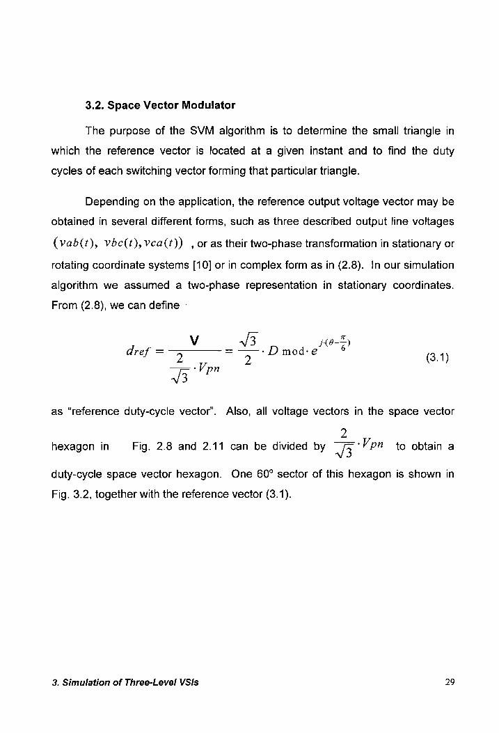
3.2. Space Vector Modulator
The purpose of the SVM algorithm is to determine the small triangle in
which the reference vector is located at a given instant and to find the duty
cycles of each switching vector forming that particular triangle.
Depending on the application, the reference output voltage vector may be
obtained in several different forms, such as three described output line voltages
(vab(t), vbc(t),Vvca(t)) , or as their two-phase transformation in stationary or
rotating coordinate systems [10] or in complex form as in (2.8). In our simulation
algorithm we assumed a two-phase representation in stationary coordinates.
From (2.8), we can define -
V V3 j(0-2) 5 5 -D mod-e 6 (3.1) —_.p
V3"
dref =
as “reference duty-cycle vector’. Also, all voltage vectors in the space vector
2 hexagon in Fig. 2.8 and 2.11 can be divided by 3 bPn to obtain a
duty-cycle space vector hexagon. One 60° sector of this hexagon is shown in
Fig. 3.2, together with the reference vector (3.1).
3. Simulation of Three-Level VSIs 29

A ppn B
ppo non oon i= 5 JN i=2
dp
d20 dref
000 an nnn oe] \/ PRO P > ppp d10 da oon a
Vab
Fig. 3.2. Finding the da and dg projections
3. Simulation of Three-Level VSIs 30

From the geometry in Fig. 3.2., the projection of the reference vector on a and £8
axis is written as
da = aes D mod- cos(@ — 30°), and
(3.2) dp = 8 - D mod: sin(@ — 30°)
where
O=a-t. (3.3)
In Equation 3.2, D mod is the modulation index and @ is the frequency
of the output voltage. In addition to da and df parameters, the followings
are the other inputs of the algorithm:
T the switching period
TT two times of the switching period
fon very small transition time
D mod modulation index, 0 < Dmod < 1
x the parameter that divides the small vectors into
two pieces. For example, if the duty cycle of the small vector is d@01 then,
d0lp=x-d01,and d01n = (1— x)-d01 which are the duty cycles of
the positive and negative small vectors.
In Fig. 3.3., 210 and @20 represents the projection of the reference
vector on the apexes of the large equilateral triangle. This duty cycles are used
to determine the small equilateral triangle where the reference vector is located
and to find the duty cycles of the space vectors which form the small equilateral
triangles.
3. Simulation of Three-Level VSIs 31

Space Vector Modulation algorithm, first of all, finds the location of the
ches
reference vector in the large hexagon, i.e. determination of the “i” parameter,
where i=1,2,...,6. This is done by comparing the sign of the alpha and beta
projections. For example, for i=2 sixty degree interval, da-dB>O and
df > 0. The other sixty degree intervals are determined the same way.
3. Simulation of Three-Level VSIs 32

i=2
/ \ YY d20 ae dref Lee
” \ 7
\ °
/ ©& Y /
/ dx /
A /
/
y /
1 d10 a vA
Vab
Fig. 3.3. Finding dx
3. Simulation of Three-Level VSIs 33

Second, to determine in which small triangle the reference vector is, i.e. to
find the “j” parameter, where j=1,2,3,4, we need to find the dio and d20 duty
cycles. Then there are four options:
1) If dio is larger than 0.5 then the reference vector is located in j=1
triangle. Then duty cycles for the vectors forming this triangle are
calculated as in Appendix B.
2) If d20 is larger than 0.5 then the reference vector is located in j=3
triangle, and then duty cycles are calculated the same way.
3) If 1 and 2 or nor true, then reference vector is located in j=2 or j=1. In
this point an other parameter is necessary to define, i.e. de. The
parameter dx is the projection of the reference vector on the axis
where the medium vectors are located. For i=2 sixty degree interval,
3 Oo
dx = 5 D mod: cos(@ — 60° ) (3.4)
and since cosine is an even function whether @ is less or bigger than
30° does not make and difference. Then, if dx is larger than v3 4 , the
reference vector is located in j=2 triangle, if not, then it is located in j=4
triangle. The parameter dr can be calculated the same way for other
sixty degree intervals.
Fig. 3.4. shows all 24 small equilateral triangles. Above explained
algorithm finds the i,j combination for a given reference vector which can be
anywhere inside the large hexagon.
The complete SVM algorithm as a flow chart is given in Appendix D.
3. Simulation of Three-Level VSIs 34

Fig. 3.4. Each small equilateral triangle is represented by i,j combinations
3. Simulation of Three-Level VSIs 35

3.3. Simulation Results
Saber simulation of a 250 kW three-phase three-level VSI is performed to
test the SVM algorithm, to observe if the voltage across the input capacitors are
constant at half of the DC bus voltage, and to determine the inductor which gives
20 % current ripple. The most important reason of simulation is to test the SVM
algorithm. The same algorithm can be easily implemented on a DSP board for a
prototype circuit. Fig. 3.5. shows the circuit parameters used to get the time
domain results. Output line frequency is chosen as 60 Hz. One cycle simulation
of three-phase three-level VSI on a Sun Sparc Station 10 takes about 3 hours.
The following voltages and currents in Fig. 3.5. are chosen as simulation outputs.
Output line currents (7a ,7b ,Ic )
Harmonic content of the output currents,
Output line to line voltages (vab ,vAB, VBC , VCA), and
Midpoint voltage, -vn.
Fig. 3.6. and 3.7. show the output line currents in one cycle and in a sixty
degree interval. It can be seen from the results that, peak line current is 210 A,
and peak-to-peak ripple is about 20 %. Sixty degree interval of line currents
shows that current crossing is smooth. Line currents cross each other at every
sixty degrees where the reference vector moves from one sixty degree interval to
an other. SVM algorithm should be good enough to provide a smooth current
crossing.
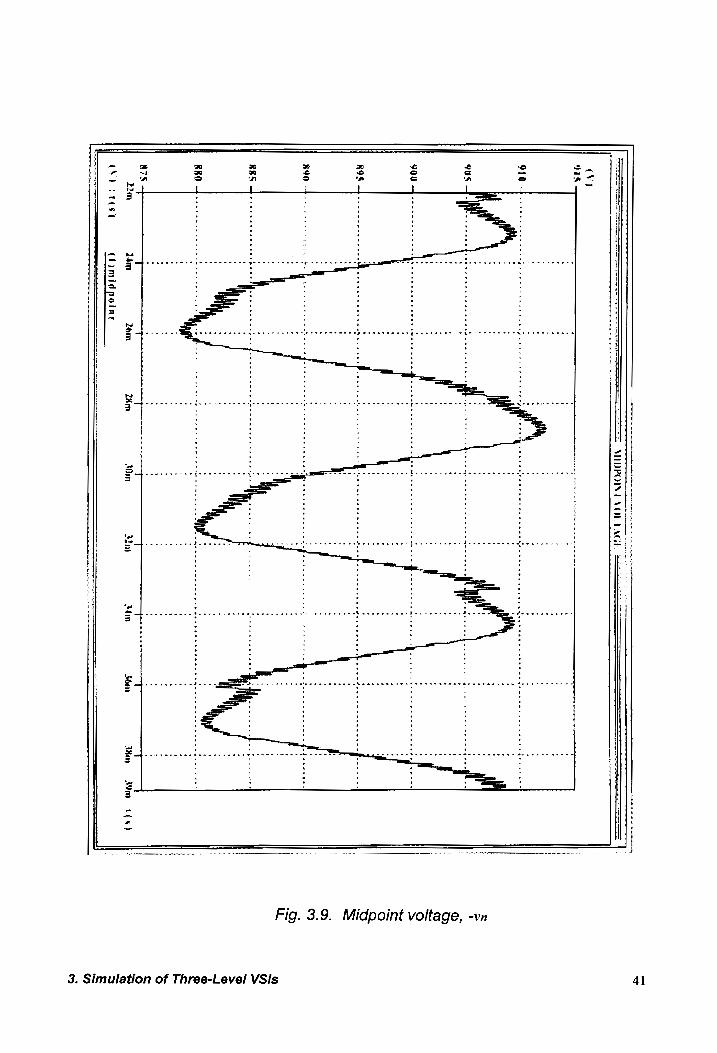
Fig. 3.8. shows the output line-to-line voltages before and after the output
filter. Line to line voltage before the output filter is a time discontinuous voltage
and has zero, half of the line voltage and full dc-bus voltage in each direction,
which is a distinct feature of a three-level VSI. Fig. 3.9. shows the midpoint
voltage which is constant at half of the dc-bus voltage but has a third order low
frequency swing. This voltage swing is caused by medium vectors. As rotating
vector moves close to medium vectors, one of the capacitors are discharged
slightly more than the other.
3. Simulation of Three-Level VSIs 36

$1 $3 S5
11 Sz S 44\ S 66\ a A id
1800 V a = 3
TF S11
S2
Fig. 3.5. Circuit parameters for Saber simulation
3. Simulation of Three-Level VS/Is 37

, EC , la, ib
38
: a
OUTPUT CORRES TS
(¥)
250 5
: :
: hn.
; a
: :
: :
‘le i
2H) whetenceesens
‘ tees
setae eee
‘ 7
5 i
140 +
veer cereeeedeeuee
a ebavaees
; ;
: :
‘
: :
+ £
4 ‘
. ‘
> #
4 '
: °
' :
‘ :
; RW
paren
ce eeee
ee a
potrrcetetesse
se
i
aa
* winter edeaee
wee
eete
; seats caubaneaee
vi ;
: '
ii. :
; :
: ‘
x .
. .
~ a
: ‘
HE
. aft
’ a
x '
‘ :
t ks
. al
' ®
x Ai
* i
; t
: "Ra:
: :
A :
i wine
menwacne
wane
wen b enn
ne ee
wahee rs
en sere
eune Av ewe ree
em OERE
wae eee eee
: :
fs - 7
‘ .
: :
mn :
: ®
t ‘
“a:
‘ a
x t
. 1
cf a
“”
; ;
: :
; :
a a
* :
: .
a r
. .
’ :
=; ‘
‘ ;
: :
: ~ES6
~~ .
abv
yA
ew
a ee
nwa hbwwn
= all
Wane Rete saree ren
are awe
wee
me
; '
; oe
' 4
* t
1’ s
+ ,
i
a x
t a
» +
vi \
: .
' z
t @
' +
> ‘
‘ ‘
: ;
‘ '
; ;
; ;
.
R
‘ ’
* ’
a ‘
’ i
am Jim
26m 28m
Mra a4m
36m in
Sma)
(Ad S08)
(Poi¢hitad
CEYECT Eby
(bidi.de)
Fig. 3.6. Output line currents
3. Simulation of Three-Level VSIs

OVTPTD
LINE CURRENES,
fe 10
ki
39
- 3
3 :
: :
: 3
3 :
ig :
: :
; ib:
' Fah
ON ay :
; :
; ry
WV ahs he
Poorer
tresses ecbsc rcs secsscdscerscsccs seb sescscecs
esses ssc es ss
“etarcanb eee
aa
: vi
Wn y
: :
: h
if ai alse!
eee Fe
; hy
; aA, A:
ayy
ee .
’ a
3 4
ia .
'
4 Hi :
i Uy
: !
TOU dace
cence
cee eee abe
entered
eee etree
be: RV
De ceeee ccc
he ce een
ees :
: toa
fuels ‘
: 2k
e ‘
‘ ’
. A
3 i
Woq
+ .
; ;
: wifey
fo:
WW ;
: SQ
4------
treed cen
eee rere beseteen
rere ter
esp AMES 4 Ae
eee eee
ee wenn
ngel tA
de cree
eed
ser
rece nee
n eae
renee
tore ;
Tien fh
; :
Dk
age MUD
| ;
vee
TUK
U yevner codes
the iw AP
re weer een
ree wet
eset
et tee
ene nee
ven eee
eet eaee ek
fe . yh:
tara enatavaevereees
* A
i eu
} «
« \:
* ,
' iy!
‘ ‘
a AN
‘
> , Band ay
¢ ‘
: re
: .
f m4
y ’
' ’
hk, 1
w iyew
; LA
~Sfp -p-.----
vy
7h eames
ee rer
Oe
ene eee
ee de eee
ee ee
44 *
i; ~ = ~
‘ “1.
‘ ~
r : : a
ee ee
: : : : :
ww eh
* * a ‘ ‘ ’ » 5 ‘ r * ‘ x * x 2 , ‘ ;
Fer
aee era
rd
ern
ene
ee
‘ ‘ ‘ ' t é , , 4 ‘ n ‘ ‘ ' , ’ r . ‘ . * * +
ty degree interval in a six Fig. 3.7. Output line currents
3. Simulation of Three-Level VSIs

40
aa . SR SST
H
er UT VOr
j 4 EN eee ese
ee acai s
ienna
Sihtt
(Vp
rates Ferree
erent, meme
wien tea
TK
VCA =
‘
seca seepe 4 wae . « ' . ’ ’ a , » + x ¥ * . £ ’ € ' >
* melt t
y,
/
‘ a
mene
wma cee ened wenn nnn eae ‘
Ain
ie
eee
Itages, vab, vAB, VBC, and vCA ine vo -to-| Fig. 3.8. Output line
3. Simulation of Three-Level VSIs
Frye tet
. .
. .
. 1 =o
t errereeerrrrrrrererrrrmnennagaenatananaemnnnreeyshtttOC
HPAI
MOOIRARO OPEC HAAS
—————— =
=
SE
VIDPOIND VOL
PAGE
iv)
:
y18 . ®
‘ ‘
+ .
. r
’ E
“ '
. 8
r ¥
» a
i '
‘ 1
‘ «
* ’
» .
‘ t
* +
‘ ‘
. .
¢ ’
* °
a ‘
‘ .
‘ ‘
. +
é »
. *
' ‘
j ‘
‘ 1
‘ ®
. .
a 7
x ’
’ .
’ ®
‘ *
D ’
4 2
* *
+ ‘
* A
1 ,
, .
4 910
+ ‘
» ‘
‘ ‘
7 ‘
. —
BEM ee
a pe ee gE
em
ad
wel
ree a Rm
CONE ERR HEHEHE
HER MEE
HAE EEE
RE
TR QRH
EH Reese remy
eK ETT
h .
’ ‘
* ’
‘ .
i .
. t
’ an
’ ’
+ ¢
* *
A ,
2
A ’
7 A
4 '
n *
’ :
E Hy
+ ‘
‘ .
x 1
a F
s ‘
' ’
‘ee ‘
‘ F
A ‘
2 .
a ‘
‘ .
avy
’ ‘
: u
4 »
4 ‘
. ]
Ny .
’ ’
‘ +
’ ’
‘ tf
‘ ‘
‘ ous
fit .
. j
’ ‘
. AH
. ‘
‘ :
. wt
ewe
Ga weee
rare meee
ew
eee
ee apt
rr re
rete
een meme
ne eee oe
of ctw web ete ey RM
Eee
ae 2
x ‘
’ :
j .
, '
4 *
* ‘
. .
1 ,
,
‘ *
H a
a «
. ‘
. .
7 ‘
t r
’ ’
' 1
ao A
a .
. .
’ ,
. .
‘ .
s .
. ‘
' +
y ’
’ .
; ®
. *
. s
, .
7 +
, a
. .
’ *
* .
, .
& '
. ’
' ,
. .
. i
QO a
nw eee
cre meee cee he ecm
cee ees
banat wee etter
cee te
Becca ee
Bb
de even
eet
en eedebew eee
‘ ,
> .
' v
2 .
‘ ‘
® *
4 Ls
* *
.
‘ '
. 4
‘ .
* ‘
a .
. 7
. ’
. *
5 ‘
‘ .
’ +
' ®
‘ ’
f .
. ‘
4 .
’ .
‘ 4
ROS
poe
cnn eee
ee Meee
e ener
ek ne cee
erence ates
Zescceewasbereadaccnmnnen nena Bees
anes .
. ‘
4 .
* .
. i
® ‘
+ .
. !
, '
” ry
, iy
. ‘
. ‘
‘ '
¥ '
+ ‘
‘ ‘
4 .
’ -
‘ ‘
. ‘
7 +
‘ '
+ ,
1 .
’ ‘
x .
’ .
’ .
BOO
HP ee
be ig
ee eee ee
dena
cs see
amen
wee eens
Hoc n eens Hae
deen renee
en ee fala
nnener «
* 4
+ .
, 1
’ .
. .
qa +
* .
P ‘
‘ .
‘ «
+ *
. i
e '
. x
. +
’ .
4 .
7 '
+ +
*
4 +
' :
" £
. ‘
. .
‘ Zz
‘ 4
. '
. +
. e
. .
« .
x
8 §
’ ,
‘ ‘
* *
4 a
4 ‘
i} .
a .
. .
if The
*
. +
1 ly
: Fi
tn *
‘ fl
‘ .
’ ’
' 4
' .
. rT
. ’
.
‘ ’
» .
. r
' ’
’ +
. ’
' :
. ‘
. ,
» ‘
an
‘ .
. *
’ ®
' u
. '
‘ ;
. .
‘ a
+ i
a! ‘
‘ .
. ‘
. .
. +
x ”
' a
a
‘ ‘
* +
+ '
’ :
. +
. 1
a 1
t f
& '
’ *
¥ 1
* i
® 4
. ‘
. ‘
‘ *
, ’
. ‘
1 ”
‘ e
. ,
. ‘
* .
© a
’ ‘
. *
u78 '
, °
1 q
q ’
1 i
i
22m dim
tom Wm
(Vo itis)
(l)midpoinr
+ - xs
‘oe > = = =
Wa
Asm tis)
41
Fig. 3.9. Midpoint voltage, -vn
3. Simulation of Three-Level VSis

This happens six times in one cycle since there are six medium vectors in one
cycle, which results in a third order harmonic. Further improvements on SVM
modulation can be done to reduce the magnitude of the low frequency harmonic.
An other important output of the simulation is the output current
harmonics. Fig. 3.10. and 3.11. show the harmonics content of the output
currents for low and high frequencies. It can be seen that the output current has
a strong component at 60 Hz, and very weak 5", 7", 15", and 19" harmonics.
Other harmonics are at the multiples of switching frequency (10 kHz) and their
size is determined by output filter design.
3. Simulation of Three-Level VSis 42

——————————
Pup!
Current
Spectrum
at Low
tr rere ERRNO
Fivguencies ===
i ; i i
DBZ) 50
os
z ;
. :
: ;
7 ™
< h
i ,
+ y
' ,
, .
x s
: ‘
x ‘
* ‘
‘ *
e ’
: :
. .
< x
» *
> ’
* t
> +
. x
t t
. *
* ’
‘ *
. '
’ .
* :
® 2
‘ °
‘ ,
‘ 40
: ‘
: ,
‘ .
‘ ,
‘ )
wecead
+-
PT
ne ee
ee
ne eee
Ee
ee PATER
EERO
ORE
UR
ew
eee ®
: .
’ :
* :
$ ’
x ,
x ‘
x *
’ '
, <
. >
, .
? +
' 4
* ‘
> ,
* >
‘ a
; .
1 *
* >
a .
» .
> '
* ’
‘ a
‘ ‘
‘ 0
x ,
« ‘
2 ‘
. :
’ AQ
m+} Pree
eee D
RO
nyt ee ee
tet eee
gee ee cee
epee eee
eee
eee
eee
re ee
ee ee ee eA
NA +
f 4
' 4
’ ’
' .
. ‘
. ‘
: .
a ,
® 7
T ‘
¥ 2
' 4
+ ,
‘ ,
‘ .
. ’
* +
5 2
‘ *
x .
> ‘
> <
, ‘
> .
* ‘
‘ x
. 4
+ '
’ +
. ’
. ,
+ 204.
ar a
BRE MET
AT ERE
TOR ARS
DEON PEE
RE Ce
ee
Om ee ee
Oa ee
ee ee Oe
t '
a 2
¥ :
. *
* .
‘ »
x ‘
’ ‘
& *
t ’
‘ +
a a
' *
4
' ‘
, =
a a
. o
+
+ ,
’ *
: *
. °
‘ '
’ ‘
. ‘
‘ ‘
Q >
, ‘
, <
' ,
. .
5 tis
|.
ew
enn
es ewe
ee ane tem wae
Wee eee
ee ee
SR Rm
ee
a ee mea
: :
. $
' ‘
: :
* ‘
‘ ‘
a ‘
» x
’ t
. ‘
‘ ‘
+ .
‘ *
, :
, ‘
' .
: 1
: ‘
‘ “
. >
, ¥
> *
‘ ‘
, .
. ,
® *
+ '
i :
> +
‘ ‘
x .
’ ‘
g—-
”
erarae
ene ewewas
wee
me
we ee
wee
eee EH
ee
4 t
ev
abs
we eee Hew
ee ee
wed
+ *
. a
a x
’ .
a
‘ .
7:
¥ ‘
a ‘
' x
x ‘
. ,
. 4
’ a
* '
* s
a ’
. &
J '
x :
‘ i
' ’
t .
a ©
t .
a ‘
, «
| :
S aN
Uf a NU
; ee
; '
«If
wavanneast t.
* wedten
eg cr naadoneaee
Beene ce eneaads
Lerner sgxeeacly
tome erc gees
. .
i *
f '
“ 4‘
4 u
' ‘
. ‘
x ,
‘ ’
’ .
' *
‘ +
a ‘
. 4
t s
’ .
é a
t .
t iT
’ i
’ .
1
:
® ‘
é +
‘ ‘
e ‘
i :
: a
‘ .
; :
: '
: :
: ¢
: ‘
‘ :
: ‘
‘ :
1 :
29 |
‘ a
3 a
‘ ’
‘ ,
a ‘
* ;
“2 FRR
ee eee
OR OTe
eee ee
ee wee
ener
eRe
te ee
tee nee eee eng eee
3 é
; :
‘ ;
: :
} ‘
: i
: :
; i
; i
: :
5 :
% t
a '
t iy
t .
e l
i
4 ,
t ‘
i *
t ‘
, ‘
> ’
i ‘
‘ ?
> .
> :
* i
> ‘
4 ‘
a m
‘ ‘
: 5
iS .
5 *
s ‘
* :
' +
z ‘
i ‘
‘ 5
‘ i
> :
: .
5 :
: a
w Af
MPP ANS
STH TERS
TENT EMER
MOR TT
TT er eet
re Ee Re
me ep
ew
EE LRA
AA eee
eed
. :
i ’
i .
’ .
* s
? ¥
a ’
, a
. ‘
x *
, +
‘ s
1 ’
t ,
, >
~ I
. ’
a ‘
a ’
a ’
. <
a .
i 1
* 4
4 u
+ ‘
* 2
i | ‘a
’ i
i ‘
y a
. ’
> .
+ i
‘ ¥
I t
f .
* ~
. 1
‘ a
I z
ef ad nce
eee cee
ee ee
De cece Mca
cece
renege nee
remanent erent
enen ep ean
clin
ew cient
n ern
nna devas
0
: 1
* ,
. *
+ ‘
‘ 1
5 ‘
: a
: 5
: :
: ‘
t :
‘ 1:
: .
x *
§ *
* x
. 1
‘ i
. 3
5 *
i a
4 t
5 ,
‘ a
s ‘
, x
8
a &
a ’
5
’ '
' ‘
J *
‘ :
1 .
’ ‘
: :
: ‘
3 :
t :
: '
SY mp
enn ne
eee cee
eee
een cw
nm Men
ee eee ia
ene eee
needa
eenemannamancaemenazn bes
cc cmenccses
ements wens
nee
« .
: &
' s
s ‘
, +
a
* ¥
a ‘
i *
‘ ‘
, 1
> ‘
. s
, *
, *
. z
‘ :
, a
; 8
: ‘
: :
1 :
: i
’ ’
‘ x
‘ s
» *
: 2
: A
: t
* ‘
‘ °
a :
x t
x ’
’ *
t ’
* x
+ 60
a —
a 5k
Ll “
f 1
t ;
| |
’ t
rer }
720 R30
ad Lik
12K
fitz) a
12a 240
3ot 480
600 ?
HE fl
4 i
DAIPH2)
2 {CH
43
Fig. 3.10. Harmonic content of output current, ia
3. Simulation of Three-Level VSis

oS _ wm ‘eet
— we
‘wre _ ea —_
x ‘ . * , e ‘ = 4 bo Ww hie eae ap — ‘ . ns
— = = = & = = = bing oe i ta = = ot = = = ex
= E j | E j { i 1 Le i
—_— Pa * - » 7 4 * e ~
< © : . . a ‘ + . & t + a a * * «
ey . ‘ ; . ‘ " ‘ . cue ® , ‘ * . ‘ * :
. . . a a , x » e ry ’ 4 Kr t
crn ee ee ee ec ee ‘~_ enact ee wh eK eH Oe KE er reaewee Renna nt ene wee ee Khe ewe ww
r ' 7 s a o
. * . s a . x
ry 5 . a 4 . ” . ‘ . ‘ a + . . : “ a ‘ * > . * * 4 > e x
' ' ‘ * ‘ “ * rie . t * a . .
SH ak me eae hee mee ew dee ewes 6 I eee oe SERRA DO OER A Te ee ee = ® * * ‘ + :
. * . . 2 . ® r . ‘ > + : a 1 * 5 « . « *
” 1 * o i} e “a
r t . + a * «
. . * * ‘ ‘ x ‘ “~~ owe . = e * « . s ‘ *
ae a a a am Ce ee ee ee — = « . o cf . . « * *~ +
—- * ‘ . « : ’ « « . ©. * e . +. ¢
“nm . t * * a e e x s
mes x . a7 ® « * ‘ . €
. - c ¥ t . a « * 4
mens * * * s t a a *
ry bea * ¥ ‘ . “ a“ = * r * * a « ome wh wm Pe eneer eden epee eens ee ee = “« r * ” e + e
. . > ’ ’ « 3 ” r 4 ' a « « . * ; . . : ‘ t ‘ . , : . : . ‘ >
we a 3 7 * a < o
4 2 : : : 2 coef we 3 wep sera weee ee ee ee =
r 2 ‘ . ' . = ‘ * ‘ . ‘
4 . ‘ > J * . ‘ : ‘ = a t » * ~~
+ . « £
. . a : ‘ fea 2 ‘ . , “y mt ee ee te ee ee “= , ’ ‘ ‘ .
« . . a “ 2 ’ + ‘ ’ ~t « ‘ : ‘ ‘ o a * t , *
+ ‘ : ‘ ‘ = hand CT + . . . > ~_
. . . : : : tnd ~ BOREDOM ew ee ew HG oF: x . . . . + a =
: ‘ . , . : ° * . e t + cae]
‘ ’ * . > ‘ ~ a ’ ‘ + e 2 —
a 4 « . . 2 a én € a + . € a x
x ‘ . x . +
Hob wee ee web ed wees meen eae 3 a ‘ « * if ‘*
: . * . ’ ; : it ‘ . . ‘ ‘ ‘ ‘ . : ? ‘ a « t .
' 4 * . e
‘ + a ‘ , cone vae Vee mead aww ence tee ce cee de vee intron ecmee: : . ‘ ‘ 3
z a + * .
, ' ‘ . s a i ' . e
. i 4 . :
x + t * e
. ‘ ' . . LA * 1 . ‘
rr bnew ewe b aces eden cena dance eta cena ” 1 4 e x
5 1 1 - * ‘ 1 : >
? 1 a ea »
4 ' 4 . -
s . ‘ ’ . : 7 2] * ee x a ‘ 1 * UP a] a * = t a ' x“ < eho n= = 8 \tetattatrtetntintintata Me ne we MER ENE RR RTH APU eee Pree ee er eat eee = 4 > 2 a 1 1 a 7
. : ‘ * ‘ : ‘ > > * ’ : . ‘ : : ‘ « 4 + s . « € :
4 ul ‘ + 4 4 * +
* ‘ ’ ' ’ . ' on > ‘ ’ ' , 5 ‘ ~ a + ' . ‘ ‘ * Supe eee ee et Aaa RR EO EG ee eee Em re s ’ , ’ 4 « .
ST + ' x a ? a
’ . ¢ ' a 4 + » ‘ * . > ‘ ‘ ' ‘ « « : ’ ‘ 4 » i ’ e * * ‘ '
+ a e 1 4 t . + t ,
oa * ‘ . 4 , + * * ‘ 4
La + 1 + ' ‘ 1 x * s *
ee
(fu
Fig. 3.11. Harmonic content of the output current, ia
3. Simulation of Three-Level VSis 44
3.4 Conclusion
In this chapter, simulation of the three-phase, three-level VSI is given.
First, SVM algorithm used to build the SABER files is proposed. Sector
identification is explained for one sixty degree interval and the remaining sector
identifications are given as flow charts in Appendix D. Second, all the input
parameters for the simulation are given in detail. These parameters are
especially important for the readers who wants to implement the program on a
workstation or a DSP board. As a consequence, similar simulation can be done
easily by changing the input parameters. Then, structure of the SABER
simulation files is given for a better understanding of the simulation. Lastly, time
domain simulation results are provided for a 250 kW voltage source inverter.
Output line currents, line-to-line voltages, and midpoint voltages are obtained. In
addition to that, output current harmonics are analyzed.
Simulation results shows that the proposed SVM algorithm for a three-
phase three-level VSI works well. The same algorithm can be used in a Digital
Signal Processing (DSP) board to develop a prototype circuit. Proposed
algorithm and simulation reveals that the midpoint voltage is stable at a third
order harmonic superimposed on top of the half of the dc-bus voltage. However,
more analysis can be done to minimize the peak-to-peak ripple of third harmonic
effect at midpoint which is 1. 66 % of the dc-bus voltage for above given
operating conditions.
3. Simulation of Three-Level VSis 45
4. MODELING OF THREE-LEVEL VSlIs
Average and small signal modeling of three-level VSIs is very important
for control loop design of the converter and dynamic analysis of the system
where three-level VSI is used.
A simple model of the three-level VSI and the load is given in [9-10]. This
is a very simple description of the converter-load side behavior. However, the
dynamic description of the dc-link side and load side are not covered in the
literature. In this work, small-signal analysis of a three-phase three-level VSI
which covers the dc-side and load-side dynamics is proposed [11].
Typical assumptions for a small-signal model are:
e perturbations are much smaller than the operating point values,
e switching frequency is much higher than the output line frequency
(this is a requirement for average-model analysis), and
e all switches are assumed to be ideal and inductors, capacitors,
etc. are considered to be time invariant.
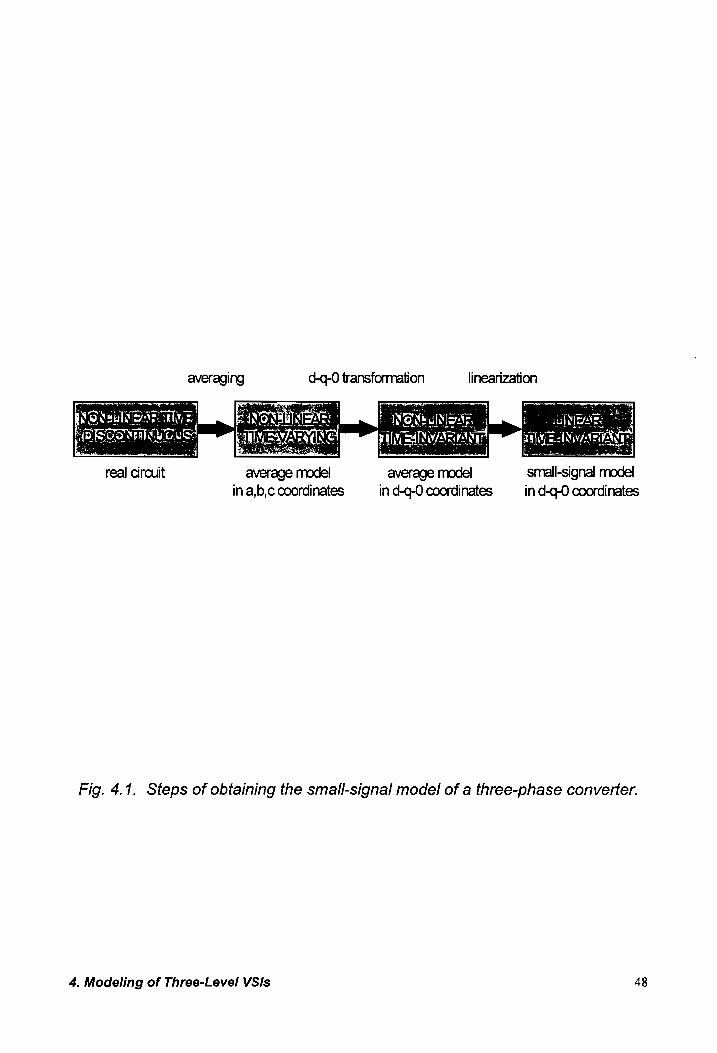
There are certain steps to follow to obtain the small-signal model of a
switching converter, Fig. 4.1.
First of all, switching function representation of the converter is proposed.
Switching function is a discontinuous function of time which completely
determines the input/output voltage/current relationships of the whole converter.
In a simple dc/dc converter, switching function is a single function of time which
takes the values of “1” and “0” meaning switch is “on” and “off’, respectively.
However, in a multiphase converter, since there are multiple input/output voltage
and currents, the switching function must be a matrix.
4. Modeling of Three-Level VS/s 46
Second, average model is obtained by applying the moving average
operator to the switching function. This results in non-linear time varying
systems equations. Then d-q-0 transformation eliminates the time variations and
gives non-linear time invariant equations.
Finally, linearization of these equations around the operating point results
in the linearized small-signal model. Desired transfer functions can be then
easily obtained from small-signal equivalent circuit. Every block in Fig. 4.1. is
explained in the following chapters.
4, Modeling of Three-Level VSI/s 47
averaging d-q-0 transformation linearization
real circuit average model average model small-signal model!
in a,b,c coordinates in d-c-0 coordinates in d-c-0 coordinates
Fig. 4.1. Steps of obtaining the small-signal model of a three-phase converter.
4. Modeling of Three-Level VSIs 48

4.1. Discontinuous Model Of The Converter
Input/output voltage and current relationship is derived in Chapter 2 as
vao Sap San y
vbo|=|Sbp Sbn|- ° =[S]-[ve] vn , and (4.1)
Vco Scp Sen
la Ip “J=([s]’ -| is In (4.2)
Ic
which is the nonlinear time discontinuos model of the converter, ie. the first
block in Fig. 4.1. Note that since there are two input voltage sources, vp, vn, and
three output voltages, the relationship between these two voltages must be a
matrix with a dimension of 3X2. In addition to above equations, from Fig. 4.2.,
dynamic equations of input dc-capacitors can be written as:
dvp | -_¢q dvn dt Ip = Cc dt in, (4.3)
where Cl = C2 = Cdc. Assuming the L,C, and R are the same in every
idc = Cdc
phase, the relationship between line-to-midpoint voltages and the voltage
between output ground and midpoint, i.e. VNO , is
vao + vbot+ Veo vNO = 3 . (4.4)
4, Modeling of Three-Level VS/Is 49

Vpn . San 9
vn Tm C2
in
5 4
Fig. 4.2 Switching function representation of three-phase three-level VS!
4, Modeling of Three-Level VSIs 50
4.2. Average Model
Moving average of a periodic function x(t) over one switching cycle is
defined as:
t _ 1 X(th=>-: [xte-de (4.5)
Tec t—T,
where x(t) represents the instantaneous value of currents or voltages [12].
Average model of three-level VSI is obtained by applying the moving average
operator to (4.1) and (4.2), where input voltages Vp , and Vn are assumed to
be constant over a switching period. Then, average model input-output voltage
relationship is
Vao dap dan Vp
vbo|=| dbp dbn|\- =ld|- moe p " vn | vn (4.6) Vco dep den
where duty cycles dap, dbp, dep are average three-phase duty cycles.
Input-output current relationship becomes,
r la
P _ T Va
a = la} |i , (4.7)
where
iptint+io=0. (4.8)
4. Modeling of Three-Level VSIs 51
State equations with averaged current and voltage in a,b,c coordinates can be
obtained by KVL and KCL from the circuit in Fig. 4.2. They can be written as:
] Vvao — VNO
dt|xv| | 1 1 ‘Tx |7| 4 | Pee PO an i383 — R.cs 03x3 Vco - VNO
(4.9) 1 1 1 | — ———dap -——dbp -——d Ta.
a ~| Cde P Caes Cae i+) C4 |. Fac dt | vn I I | :
——dan — dbn ———dcn A. Cde Cac Cde Cae where,
ia VAN
xi=|ib Xv =| VBN ; oy (4.10) Cc
are the average currents and voltages. In (4.9), 03x3, and /3x3 are 3x3 zero and
identity matrices, respectively. From (4.9) average model circuit of a three-
phase three-level VSI can be obtained as in Fig. 4.3. In average model, instead
of output line-to-line voltages, line-to-midpoint voltages are considered to
observe the midpoint dynamics.
4, Modeling of Three-Level VSI/s 52

Vao © Sr
—-+4
>
vp ; Vbo 5
Von = -} > © o g <{> 5 >
gr
H+:
Vco » $m
rk
OQ ;
Fig. 4.3. Average circuit model of a three-phase three-level VS!
4, Modeling of Three-Level VSis 53

4.3 d-q-0 Transformation
4.3.1 State-Space Model in d-q-0 Coordinate Frame
D-q-0 model of the converter can be obtained by multiplying the both
sides of (4.9) by transformation matrix T, which is defined as:
cos(w.t-d) cos(w,t— 2n/, —O0) cos(w.t— Any, — 6) 2
T(w,t) = 3) —sin(w,t— 3) —sin(w,t— anf, —6) —sin(w,t _41/, 6)
Lp Ln La
where W,is the angular frequency of the rotating d-q-0 frame, and 6 is the
> (4.11)
phase shift between a,b,c and d-q-0 coordinates [10]. Note that matrix T is an
orthonormal matrix, i.e. 77 =77'. When transformation is applied to (4.6) and
(4.7), the relationships between input-output voltages and currents become
vd dpd dnd| -_ vp
vq |=|dpq_ dng |- : Vn
v0 dp0 dn0
= iYd 1p dpd dpq _ dp0 ‘
in| |dnd dnq dnd 4 , (4.13)
‘yo
Ld
, and (4.12)
where
4, Modeling of Three-Level VSIs 54
vd 1Yd dpd dnd
Vv ; dog a qT} NG) ong | PI 4
v0 1Y0 dp0 dno
are the d-q-0 transformation of
Vao ia dap dan
v ib dbp db vbo | | and /p n
Vco le dcp den
respectively. The following assumptions are considered while average model of
three-level converter is obtained in d-q-0 coordinates.
e Load and low-pass filter components are symmetric, i.e. 2¥0=0 and
vY0=0, and
e “p” and “n” rail duty cycles are assumed to be equal and with a 180°
phase shift.
State-space model of three-level VSI in d-q-0 coordinate frame can be written as:
; ; | dpd/ dnd/| i¥d | , Mh O, 0 , nd/, i¥d 0 | vYd Me - Voc 0 Q, 0 0 | | vyd 0
d| i¥q - 0, 0 0 Vy dbay, dngy i¥g oT. dt VY ~ — | _1 VY * 0 “tae q 0 oO, C RC 0 ) q y
vp dpd dpq vp vn 7 Vt 0 7 1 Vo 0 0 0 vn Y.
Ln dnd ng L'a L/S Cade. “ Cdc 0 7 Cde 0 0 0 |
(4.14)
where d-q-0 components of output voltage and currents, and input capacitor
voltages are chosen as state variables. Selection of the output variables depend
on what to control. Output voltage d and q components and one input capacitor
voltage are chosen as the output variables. Output function can be written as:
4, Modeling of Three-Level VSIs 55

[ i¥d |
vYd v¥d 0 0 0 0 oll.
-lo 0 0 1 0 of.} 74 v¥q | = vq (4.15.) Tp 0 0 0 0 1 0 -
ls <
where
vYad
vYq
vY0O
is the d-q-0 transformation of
VAN
vBN
VCN
and v¥Y0 = 0 since the three phase output voltages are assumed to be balanced.
4.3.2 Steady State Solutions
Steady state solutions for equations (4.14) and (4.15) can be obtained by
setting the dynamic terms to zero. The results are given in (4.16), (4.17), (4.18),
and Table 4. Note that, capital letters are used to denote the steady state
solutions.
Dd = Dpd = —Dnd , (4.16)
Dq = Dpq = —Dngq, (4.17)
D0 = Dp0 = Dno, (4.18)
4, Modeling of Three-Level VS/s 56
Table 4 Steady state solutions
V pn
Vyd -(1-0,?LC)-VyYq- OF d component of the duty cycle | pg = R
Vpn
o,L 3 Vyd-——+4Vyq-(l-0,’LC)
q component of the duty cycle Dq=
zero component of the duty cycle
Do = 2(Da? + Dg?)
current d component of the output VYd
current 1¥d = “RO o,C -VY¥q
q component of the output VYq I¥q = —-+0,C -VYd
current R
zero component of the output lyo=0
4, Modeling of Three-Level VS/s 57

Input side currents and output voltages in steady state are derived the same
way, Table 5.
Table 5 Steady state solutions for input side
p rail current Ip = Dd -Id+ Dq-Iq
n rail current In = —Ip
midpoint current lo=0
d component of the output voltage VY¥d = Dd-Vpn
q component of the output voltage VY¥q = Daq-Vpn
zero component of the output voltage VYo = Q
voltage between N and midpoint VNo = 0
upper capacitor voltage Vpn
Vp=-Vn= 2
voltage ripple in midpoint Vp+Vn= 0
Average circuit model of three-level VSI in d-q-0 coordinates is given in Fig. 4.4.
4, Modeling of Three-Level VSi/s 58

ip vd. w: L-iYq iYd L
<> ><
| Vp == +
} ~ vY¥d—-—C wCv¥q SR Vpn = lo ~
—_}> oO
vn L N t ;
In vq lYq wl iYd L Q
> _ wn
+ w:C v¥d v¥¢=—C R
Fig. 4.4. Average circuit model in d-q-0 coordinates
4. Modeling of Three-Level VS/is 59
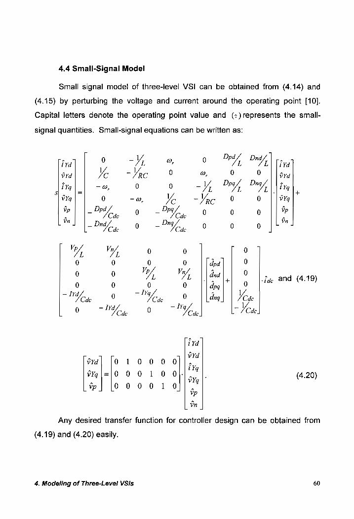
4.4 Small-Signal Model
Small signal model of three-level VSI can be obtained from (4.14) and
(4.15) by perturbing the voltage and current around the operating point [10].
Capital letters denote the operating point value and (+)represents the small-
signal quantities. Small-signal equations can be written as:
- _1 Dpd/ Dnd/\|_. - iYd 0 1 e, 0 wh "yy iYd
bYd Mo Vac 0 @, 0 0 bYd 2 _ 1 Dpgq Dngq a Fle o, 0 0 -\, v/, %,\ | iva |
VYq > -o, Lc Vac 0 0 vYq
Vp _ Dpd _ Dpq Vp 5 Cdc 0 D Cde 0 0 0 5
Ln Dnd nq pwn Cae C8 Cae 0 0 |
Vey Vn, 0 0 r Oo 7 0 0 0 0 dpd 0
Vp Vn 5 0 0 0 Y, M1 || dna | tae and (4.19) 0 0 0 0 dq 0
— ]¥d — I¥q A 1 Yo 0 Cde ] 0 dnq (de
— IYd — L¥q - L 0 Cdc 0 Voie! = ee]
i ya |
vYd vYd 0100 0 O]].4 A 1Yq v¥¢gi=|0 0 0 1 O O}- sy, | (4.20)
VY
i | |0 0001 0|| .” vp
Any desired transfer function for controller design can be obtained from
(4.19) and (4.20) easily.
4. Modeling of Three-Level VSIs 60
4.5 Bode Plots of Transfer Functions
Small-signal model of the three-level converter is a sixth order system.
That is why it is very difficult to obtain the analytical expressions for transfer
functions. Instead of that, state-space matrices are used to get the desired bode
plots. MatLab program is used to obtain the Bode plots. The parameters in
Table 6 are chosen as the operating point values.
Note that, parameters in Table 6 are the same parameters as in SABER
simulation. Two transfer functions are given in Fig. 4.5. These transfer functions
give the information about the poles, zeros, and the dc-gain which are necessary
for the control loop design. The rest of the transfer functions are given in
Appendix E.
In order to verify the circuit model in Fig. 4.4, a PSPICE [13] simulation is
performed by using the parameters given in Table 6. The linearization was done
by PSPICE program. The simulation results and files are presented in
Appendix F. The frequency response given in Fig. 4.5(b) matches with the
simulation results given in Appendix F.
4, Modeling of Three-Level VSIs 61

Table 6 Operating point values for small-signal analysis
dc-link voltage Vpn=1800 V
power level Po=250 kW
line current current la=210 A
balanced resistive load R=469
output inductor L=0.25 mH
output capacitor C=100 uF
dc-link capacitors C1=C2=Cdc=1 MF
4. Modeling of Three-Level VSIs 62

107 10° 10 Frequency (rad/sec)
7 TOY YT Pray if TOY e etree : oe oe ereeal ee er we ot ate te ee ee ee ee a ee
. . tees erp sce tee seat i 2
10 Frequency (rad/sec)
Fig. 4.5. (a) Frequency response of i y/. .
4, Modeling of Three-Level VSis 63

Gain
dB
Phas
e de
g
—1680
Frequency (rad/sec)
Fig. 4.5.(b) Frequency response of i ty/, pg
4. Modeling of Three-Level VSis
64

4.6 Conclusions
In this chapter, average and small-signal analysis of the three-phase
three-level VSI were developed for the first time. Switching function
representation, and average models in a,b,c and d-q-0 coordinates are derived.
Several transfer functions are obtained from small-signal equivalent circuit.
Control variables of the model are the duty cycles of single-pole-triple-throw
switches. Two duty cycles from each single-pole-triple-throw switch should be
known, which results in total six control variables. As of the output variable, two
output line-to-line voltages, or currents, and two input capacitors voltages can be
controlled.
Contribution to this point is the development of SVM algorithm, verification
of the algorithm by SABER simulation and development of the small-signal
modeling of the converter. However, for a complete closed-loop analysis, and
system level experiments, an error compensator and small-signal model of SVM
block need to be investigated as future work.
4, Modeling of Three-Level VSis 65
5. SUMMARY AND FUTURE WORK
Three-phase three-level voltage source inverters (VSIs) are very attractive
for high-voltage and high-power applications. The most important advantages of
a three-level VSI compared with a conventional two-level VSI, for the same
power level and switching frequency are:
e only half of the dc-link voltage is applied to the switches,
e switching losses are reduced, and
e output harmonics are reduced.
The disadvantages of a three-level VSI are high number of devices and voltage
balance of the dc-link capacitors.
In this work, three-phase three-level VSI are investigated. Operation
principle of the converter is explained by switching functions. There are three
output voltages and two input voltages. The functional relationship between
input and output voltages must be a matrix of 3x2. Note that in a conventional
two-level VSI this relationship is a 3x1 array.
Space Vector Modulation (SVM) of three-level VSI is proposed. There are
total 3 zero and 24 non-zero switching vectors. Which vector to chose is a very
important subject. To achieve sector identification, a modulation algorithm is
proposed. Duty cycle calculations for all sectors is given. A Digital Signal
Processor can be used in order to calculate the duty cycles in the application.
A comprehensive SABER program is developed to verify the proposed
SVM algorithm. Algorthm is tested in a 250 kW three-phase three-level VSI. All
duty cycle calculations and flow chart of the algorithm is given in Appendixes B
and D. Simulation results reveal that the proposed modulation scheme and
5. Summary and Future Work 66

algorithm works well. There is a low frequency voltage fluctuation in the midpoint
with a peak-to-peak voltage less than 2 % of dc-link voltage. Third order voltage
swing is caused by the usage of medium vectors. However, small signal
modeling reveals that this peak-to-peak voltage swing can be further reduced.
The future work is to optimize the SVM algorithm to further minimize the
midpoint voltage. For the closed-loop operation, a feedback error amplifier can
be designed based on the small signal model and the small-signal model of SVM
block can be derived.
5. Summary and Future Work 67
i=2
j=1
VO1p poo
V1i2 pon
V1 pnn
Voi1n onn
j=1
VoO2n oon
V23 opn
V2 ppn
VO2p ppo
j=2
VO1p poo
V12 pon
Vo2n oon
VOin onn
j=2
VO3p opo
V34 npo
Vo04n noo
VO3n non
j=3
VO2p ppo
V2 ppn
V12 pon
VO2n oon
j=3
Vo3n non
V3 npn
V23 opn
VO3p opo
j=3
VO4p opp
V4 npp
V34 npo
VO4n noo
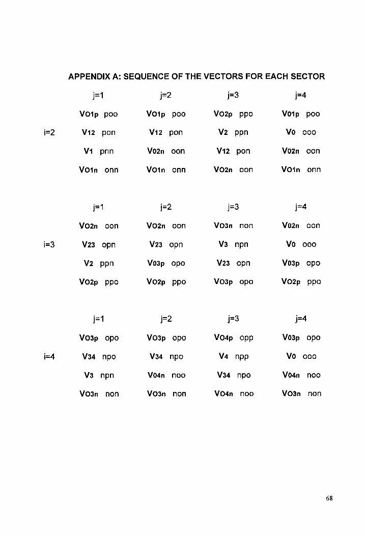
APPENDIX A: SEQUENCE OF THE VECTORS FOR EACH SECTOR
j=4
V01p poo
Vo 000
Vo2n oon
VO1n onn
j=4
Vo2n oon
Vo o00
Vo03p opo
VO2p ppo
j=4
V03p opo
Vo 000
Vo4n noo
VoO3n non
68

j=1
VO4n noo
V45 nop
V4 npp
VO4p opp
j=1
VO5p oop
V56 onp
V5 nnp
Vosn nno
j=2
VO4n noo
V45 nop
Vo05p oop
VO4p opp
j=2
VO5p oop
V56 onp
V06n ono
VO5n nno
j=2
VO6n ono
V6é1 pno
V01p poo
VO6p pop
j=3
VoO5n nno
V5 nnp
V45 nop
VO5p oop
j=3
VO6p pop
Vé pnp
V56 onp
VoO6n ono
j=3
VOin onn
V1 pnn
V6é1 pno
VOip poo
j=4
Vo4n noo
Vo ooo
Vo5p oop
VO4p opp
j=4
Vo5p oop
Vo ooo
Vo6én ono
VoO5n nno
j=4
Vo6n ono
Vo ooo
V01p poo
VO6p pop
69

APPENDIX B: DUTY CYCLE CALCULATIONS
(cin= “2. pmoa)
=2, j=1
ty, = 2°20, U— dm. cos(@ — 30") — FG )
{21,1 2d cos(030")-2 2 SOO,
4-dm-sin(@—- 30°)
Lio = T, -( ie
I=2, j=2
4-dm-sin(@— 30°)
fy =T,-- 3 )
t,, = T,-(-1+2-dm-cos(@— 30°) + 3 )
2-dm-sin(@—- 30° tor =T, (1-2-di- c0s(0-30°) + SES)
i=2, j=3
to =2-T, -(—dm.cos(@ — 30°) —- 5 )
4-dm-sin(@ — 30°) t, =7T,-(-l1+ eit B>?
2-dm-sin(@ — 30° ly =T, (2 dn: cos( 930°) — SS,
70

i=2, J=4
to =T, -(2-dm-cos(@ — 30°) V3
)
4-dm-sin(@— 30°) ton = T, -( s B )
fo = 1, - ty, — to
i=3, j=1
2-dm_sin( ~ 30"),
V3 ty =2-T-, (I-
t, =T, (-1+2-dm-cos(@-30°) + i )
2-dm-sin(@— 30°)
t,, =T -( —2-dm-cos(@— 30°))
V3
i=3, J=2
fon = 7, 1 SE 2c cos(@ ~ 30°))
2-dm-sin(@- 30°) toy = T, (1 —2-dm- cos(8— 30°) - 5
4-dm-sin(@ — 30° thy = T,-(-14 m- Sin( ) B )
71

i=3, j=3
2+-dm-sin(@ — 30°)
fy, =2-T,-d- V3 )
2-dm-sin(@ — 30° th, = T, -( - “= ) 4 2-dm-cos(@ - 30°)
2-dm-sin(@- 30°) _ |) V3
t, = T,-(-2-dm-cos(@ - 30°) +
i=3, [=4
2-dm-sin(@ —- 30")
V3 ty, = T,-(2-dm-cos(@ — 30°) +
2-dm-sin(@ — 30°) ty = T, -( V3 —2-dm-cos(@ — 30° ))
to =T; —9) -to2
i=4, j=1
2-dm-sin(@ — 30°)
thy; = T,-(2+2-dm-cos(@ —- 30°) - Gi )
Ler (Acdm: sin ~ 30") 1 3 — “s V3
toy = T, -(-2-dm-cos(9— 30°) -= 2 SO = 99), 34 = 1, -(-2-dm-cos(@—- — B 3
72

i=4, j=2
2-d a _ 0
£03 = T. -(2-dm-cos(@— 30°) + m ce 30 ) 4
t, =T-(1 4 dm: sin(@ ~ 30"),
04 ~ “sg 3
2-dm-sin(@ — 30°) ty, =T,-(-1+ B —2-dm-cos(@—- 30°))
i=4, j=3
2-dm-sin(@ — 30°
C04 = T -(2+2-dm-cos(@- 30°) - m “s ),
4-dm-sin(@— 30°) ts, = T,-( 3B
1, = T,-(-2-dm-cos(6— 30°) — SMP 3) _ 4 —4,°(-2°am- COSLG — — Fy _
3
i=4, j=4
4-dm-sin(@— 30°) to = T, + B )
5. 2'dm-sin(@— 30°) ty = T, -(-2-dm-cos(@— 30°) — i )
to = 1-191 -t2
73

i=5, j=1
2-dm:sin(9 — 30"),
V3 bo = T, -(2+2-dm-cos(@—- 30°) +
2-dm-sin(@— 30°)
t, = 7, -( B —2-dm-cos(@— 30°) —-1)
4-dm-sin(@ — 30° tys = T,-(- * )»
i=5, j=2
4-dm-sin(@ — 30°) tog = 7,-C+ B )
2-dm-sin(@ — 30°)
fos = T,-(1+2-dm-cos(@ — 30°) — 3 )
2-dm-sin(@ — 30° ty; = T, -(-1-2-dm-cos(@— 30°) - - “s )»
i=5, j=3
2-dm-sin(@ — 30°)
th; = T,-(2+2-dm-cos(@— 30°) + 3 )
2-dm-sin(@ — 30°) ,
tys = Ty -( 3B ~—2-dm-cos(@— 30°))
4 dm: sin( = 30"),
V3 t, =T.-(-1-
74

i=5, j=4
2-dm-sin(@— 30°)
V3
ty, = T, -(-2-dm-cos(@— 30°) +
4-dm-sin(@— 30°)
B ) loo =T.-(
s
to = Ts — toy —to2
i=6, j=1
4-dm-sin(@— 30°) tos = 7, -(24+ m B
t -7,.(1-° SE ) >. dm-cos(9—30°)) 2-dm-sin(@—- 30)
V3
te = T, -(2-dm-cos(@— 30°) —
i=6, j=2
2-dm_sin(9~ 30"),
V3
tos = T,:-(1—2-dm-cos(@— 30°) +
2-dm-sin(@ — 30°)
V3
fos =I, -(1+2-dm-cos(@— 30°) +
4 dm: sin(O = 30"),
V3
E56 =T,-(-1-
75

i=6, j=3
4-dm-sin(@— 30°)
tos = T+
s J3
b56 = T, (-2-dn-cos(@~ 30°) - =" SEES ))
o>. 2°dm-sin(@— 30°) t, = T,-(-1+2-dm-cos(@- 30°) - 5
i=6, j=4
2-dm-sin( - 30°) J3
ty, = T, -(-2-dm-cos(@- 30°) -
2-dm-sin(@ — 30°) 3 )
lo = I, -(2-dm-cos(@— 30°) -
fo = 1; — to; —*02
i=1, j=1
2-dm-sin(@— 30°)
tog = T, -(2-—2-dm-cos(@ — 30°) +
V3
i, =T.-(-1 4-dm-sin(@— 30°) 6°” “*s
3
2-dm-sin(@ — 30°
te = T, «(2-dm-cos(@ 30°) + ae )
76

i=1, j=2
2-dm-sin(@ — 30°)
V3 bog = T,-(1-2-dm-cos(@— 30°) -
4-dm-sin(@— 30°)
V3 lo =T -(+
2-dm-sin(@ — 30°)
V3
t,, = T.-(-1+2-dm-cos(@ — 30°) —
i=1, j=3
2-dm-sin(@ — 30°)
ty, = T,-(2-2-dm-cos(6— 30°) + V3 )
4-dm-sin(@ — 30°) tg = Lo (- V3
2-dm-sin(9- 30”), B t, =T,-(-1+2-dm-cos(@- 30°) +
i=1, j=4
_ 4: dm:sin(6 ~ 30"), V3 ty, = T, -(
2-dm-sin(@ — 30°) B ) ty =T.-(2-dm-cos(@— 30°) +
to = T, — to; — to2
77

APPENDIX C: SABER NETLIST OF THE THREE-LEVEL VSI
(This netlist is for power stage only.)
Saber netlist for three-level VSI Created by the Saber Integration Toolkit 3.4b-2.7b of Analogy, Inc. Created on November 23, 1996
uhammet Cosan Virginia Polytechnic Institute & State University
# # # # # # # #
HR HHH
FH
ide_tech..model _ls=(voh=2.8,vol=0.4,vxh=2.2,vxl=0.8,
tr=10n,tf=10n,tdon=20n, tdoff=20n)
ide_d2an.@"clock_l4#109_clock" a:clock d:@"clock_clock_l4#109_clock" m:0 = \model=_lIs ide_d2an.@"buf_l4#226_out" a:SS6 d:@"SS6_buf_l4#226_out" m:0 = model=_lIs ide_d2an.@"buf_l4#225 out" a:SS5 d:@"SS5_buf_l4#225 out" m:0 = model=_Is ide_d2an.@"buf_l4#213_out" a:SS4 d:@"SS4_buf_l4#213_out" m:0 = model=_Is ide_d2an.@"buf_l4#202_out" a:SS3 d:@"SS3_buf_l4#202_out" m:0 = model=_Is ide_d2an.@"buf_l4#200_out" a:@"n#388" d:@"n#388_buf_l4#200_out" m:0 = model=_Is ide_d2an.@"buf_l4#149_out" a:SS2 d:@"SS2_buf_l4#149_ out" m:0 = model=_lIs ide_d2an.@"inv_l4#228 out" a:SS5p d:@"SS5p_inv_l4#228 out" m:0 = model=_Is ide_d2an.@"inv_l4#227_out" a:SS6p d:@"SS6p_inv_l4#227_out" m:0 = model=_Is ide_d2an.@"inv_l4#210_out" a:SS3p d:@"SS3p_inv_l4#210_out" m:0 = model=_lIs ide_d2an.@"inv_l4#205_out" a:SS4p d:@"SS4p_inv_l4#205_ out" m:0 = model=_Is ide_d2an.@"inv_l4#133_out" a:SS1p d:@"SS1p_inv_l4#133_out" m:0 = model=_Is ide_d2an.@"inv_l4#75_out" a:SS2p d:@"SS2p_inv_l4#75_ out” m:0 = model=_ls
v.@"v_dc#60" m:0 p:@"n#384" = dc=1800 r.Rxx m:0 p:y = rnom=2meg r.@"rh#242" m:@"n#371" p:0 = rnom=1u r.Ram:y p:aa = rnom=4.6
r.Rb m:y p:bb = rnom=4.6 r.Re m:y p:cc = rnom=4.6
r.Rx m:0 p:@"n#341" = rnom=2meg |.Lo m:cc p:c = 1=0.25m, r=1m_ |.Lb m:bb p:b = |=0.25m, r=1m
|.La m:aa p:a = |=0.25m, r=1m
muh1.svm s1:1 $2:2 $3:3 $4:4 $5:5 s6:6 da:da db:db # this is the SVM file Cc.@"c#64" m:@"n#371" p: MIDPOINT = ic=900, c=1m C.@"c#62" m:MIDPOINT p:@"n#384" = ic=900, c=1m c.Ca m:@"n#341" p:aa = c=100u
c.Cb m:@"n#341" p:bb = c=100u c.Cc m:@"n#341" p:cc = c=100u c.@"c#319" m:@"n#38" p:@"n#384" = c=7n c.@"c#320" m:b p:@"n#38" = c=7n C.@"c#321" m:@"n#39" p:b = c=7n
78

C.@"c#322" m:@"n#371" p:@"n#39" = c=7n C.@"c#323" m:@"n#371" p:@"n#280" = c=7n C.@"c#324" m:@"n#280" p:a = c=7n C.@"c#325" m:a p:@"n#278" = c=7n C.@"c#326" m:@"n#278" p:@"n#384" = c=7n C.@"c#327" m:@"n#37" p:@"n#384" = c=7n C.@"c#328" m:c p:@"n#37" = c=7n C.@"c#329" m:@"n#35" p:c = c=7n C.@"c#330" m:@"n#371" p:@"n#35" = c=7n vsine.vcos m:0 p:vcos = ph=90, ampl=0.8, f=60
vsine.vsin m:0 p:vsin = ampl=0.8, f=60 d.D2 n:MIDPOINT p:@"n#280" d.D4 n:MIDPOINT p:@"n#39" d.D6 n:MIDPOINT p:@"n#35" d.D1 n:@"n#278" p:MIDPOINT d.D3 n:@"n#38" p:MIDPOINT d.D5 n:@"n#37" p:MIDPOINT inv_l4.@"inv_l4#75" out:@"SS2p_inv_l4#75_out" in:2
inv_l4.@"inv_l4#133" out:@"SS1p_inv_l4#133_out" in:1 inv_l4.@"inv_l4#205" out:@"SS4p_inv_l4#205_out" in:4
inv_l4.@"inv_l4#210" out:@"SS3p_inv_l4#210_out" in:3 inv_l4.@"inv_l4#227" out:@"SS6p_inv_l4#227_out" in:6 inv_l4.@"inv_l4#228" out:@"SS5p_inv_l4#228 out" in:5 buf_l4.@"buf_l4#149" out:@"SS2_buf_l4#149_ out" in:2 buf_l4.@"buf_l4#200" out:@"n#388_buf_l4#200_out" in:1 buf_l4.@"buf_l4#202" out:@"SS3_buf_l4#202_out" in:3 buf_l4.@"buf_l4#213" out:@"SS4_buf_l4#213_out" in:4 buf_l4.@"buf_l4#225" out:@"SS5_buf_l4#225 out" in:5 buf_l4.@"buf_l4#226" out:@"SS6_buf_l4#226 out" in:6 SW_VC.@"sw_vc#156" m:@"n#384" p:@"n#278" vm:0 vp:@"n#388" \model=(2,1m,0.1m,10meg)
SW_VC.@"sw_vc#159" m:@"n#278" p:a vm:0 vp:SS2p = model=(2,1m,0.1m, 10meg) Sw_vC.@"sw_vc#160" m:a p:@"n#280" vm:0 vp:SS1p = model=(2,1m,0.1m,10meg) Sw_VvC.@"sw_vc#161" m:@"n#280" p:@"n#371" vm:0 vp:SS2 = model=(2,1m,0.1m,10meg) SW_vc.@"sw_vc#165" m:@"n#39" p:@"n#371" vm:0 vp:SS4 = model=(2,1m,0.1m,10meg) Sw_vc.@"sw_vc#166" m:b p:@"n#39" vm:0 vp:SS3p = model=(2,1m,0.1m,10meg) SW_vc.@"sw_vc#167" m:@"n#38" p:b vm:0 vp:SS4p = model=(2,1m,0.1m,10meg) Sw_vc.@"sw_vc#168" m:@"n#384" p:@"n#38" vm:0 vp:SS3 = ic=on, \model=(2,1m,0.1m,10meg) Sw_vc.@"sw_vc#172" m:@"n#35" p:@"n#371" vm:0 vp:SS6 = model=(2,1m,0.1m,10meg) SW_VvCc.@"sw_vc#173" m:c p:@"n#35" vm:0 vp:SS5p = model=(2,1m,0.1m,10meg) SW_vc.@"sw_vc#174" m:@"n#37" p:c vm:0 vp:SS6p = model=(2,1m,0.1m,10meg) SWw_vc.@"sw_vc#175" m:@"n#384" p:@"n#37" vm:0 vp:SS5 = model=(2,1m,0.1m, 10meg)
sh.@"sh#101" out:db in:vsin gate:clock gnd:0 sh.@"sh#114” out:da in:vcos gate:clock gnd:0 clock_l4.@"clock_l4#109" clock:@"clock_clock_l4#109 clock" = freq=40000, duty=0.5
79
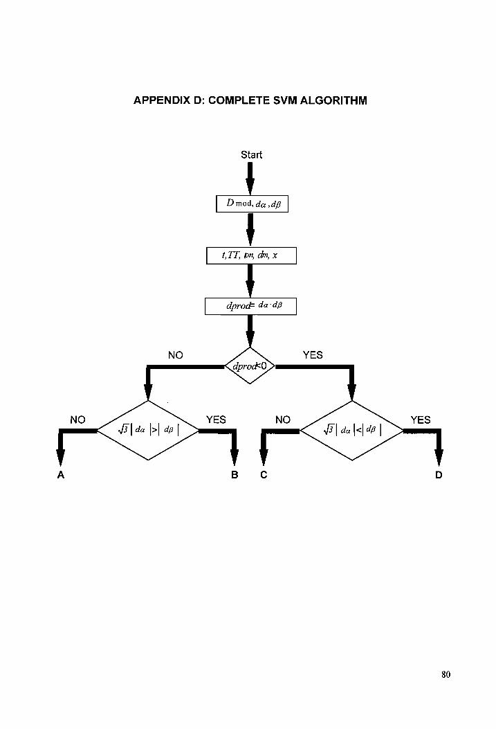
APPENDIX D: COMPLETE SVM ALGORITHM
Start
D mod, da dB
t TT. bn, dn, x
dprod= da: dp
3 | da |>| ag | V3 | da |<| 42 |
80

dx= - dp
j=
j=
YES i=
dx= dp
YES dio >0.5
NO
YES d20 >0.5
NO
YES
>0.43
NO
j=
j=
j=
81

ax = dp 5 + §3 da
dio >0.5
NO
d20 >0.5
NO
x >0.43
NO
jr4
YES
YES j=
YES
82

da dp
YES
j= Game < i090 >0.5
NO
YES
d20 >0.5
NO
YES
j= 70.43
NO
j=4
YES dio >0.5
NO
YES d20 >0.5
NO
YES >0.43
NO
j=4
j=
83

j=
dy = dB
YES
dio >0.5
NO
YES
d20 >0.5
NO
YES >0.433
NO
dx =~ dp
YES dio >0.5
NO
YES d20 >0.5
NO
YES dk>0.43
NO
j il =
j=
84

APPENDIX E: TRANSFER FUNCTIONS
vp/ dpa transfer function
150 TTT TTT Trt ToT TTT Don ketenes rrrers’ toe keane toe sees tone eenen
:
100
Gain
dB
gop:
05 a areas
10
180
120
90
Phase deg
BOL. --bet gLiitiiiii Gp idiii fb pitts PGi bt itt GE
10 10 10 10° 10° 10° 10° Frequency (rad/sec)
85
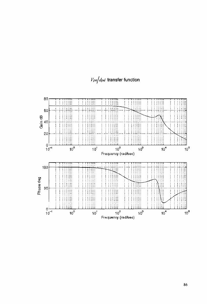
Phase
deg
180
90
Von] dpa transfer function
. # e 6p peee fee ww he we te hy te he we
. » © 4 eb bao
ee be neee . e 6 8 ewe ‘ o 6 be nnae ee ee ee oe ke ek er ee ete Feed eb hE De es ote we ote ot
o 8 @ @eeee ‘ ob # @ ota a ‘ oe @# bpeeuas
, . 2
‘ ‘
pl ar erereress | Pl a rere eres |
10’ 10° 10° 10° 10°
Frequenoy (rad/sec)
Tr TTTyT T rT TTT T ToT rT TT T TT TTT ooue ‘ » ¢ be eae « es ¢ porae 4 es 6 Panane
eee . re . se fb eee . se ee ta ee
T
10 10° 10 10 10 Frequenoy (rad/sec)
86

SIMULATION OF D-Q-0 MODEL BY PSPICE APPENDIX F
ion circui Schematics of the PSPICE simulat
GVALUE V(dd)*V(id
1 ,id2)* 1000
° G2
o id]
id2 D
° R16
sa &
AAA
ry
s a
Im b4
EVALUE
EVALUE
Im 025m
V(91.N)+(0.0377)
C8 im
cVALUE c3
-L100u °
4.6 PRIS,
a 0
N
V(q)*V(iq 1 iq2)*1000
? +7
vpn 0
—#
1800 —- —
° 5
ff
° iq!
iq2 Q1
c9 I
1m savio.n)
EVALUE Im
Vqeip.n V(id 1,
12)0(94.24 R20
Siy (id 1,
1d2)0(94.24) GVALUE
, ,
V(D.N)*(0.0377) 000q
G6 9
| id)
1d? C4
= 1000
RM 4
4.6
GVALUE] G3
V(dd)eV(id
t id2)#(- 1000)
43 330
439 ag
| V3
V4
ov Vv
R12 tk
R13 1k
G8 GVALUE
iid
.. 0
0 V(q)*V(iq
1 ,ig2)+(— 1000) q
0
87

* Schematics Netlist *
R_R8 E E6 E E7 G G6 R_R10
id1 id2 1m id1 $N_0001 VALUE { V(iq1, iq2)*(94.24) } $N_0002 iqi VALUE { V(id1, id2)*(94.24) } Q1 N VALUE { V(D,N)*(0.0377) } ND 4.6 NQ1 4.6
ND 100u NQ1 100u id2D 0.25m
p N 1800 iq2 Q1 0.25m iqi iq2 im 0 $N_0003 1m NO 1m
p $N_0003 1m 0 $N_0003 1M NO 1M Oq 1k
Odd 1k $N_0003 0 VALUE { V(dd)*V(id1,id2)*1000 } N 0 VALUE { V(dd)*V(id1 ,id2)*(-1000) } $N_0001 O VALUE { V(dd)*V(p,N) } $N_0002 0 VALUE { V(q)*V(p,N) } N 0 VALUE { V(q)*V(ig1,iq2)*(-1000) } $N_0003 0 VALUE { V(q)*V(iq1,iq2)*1000 } N D VALUE { V(Q1,N)*(0.0377) } dd 0 DC 0.7V AC OV q 0 DC 0.0145V AC 1V
88

80 + -------------------------------------------------- +--+ +--+ +--+
D3B(Z(Z2)) ~ ro
I= — _—_ 1Q0K: x= 10 Oz= 100EKz 10E= 1.0Hz
P(T(L
Ye ,
~
Simulation result of #¥4
89
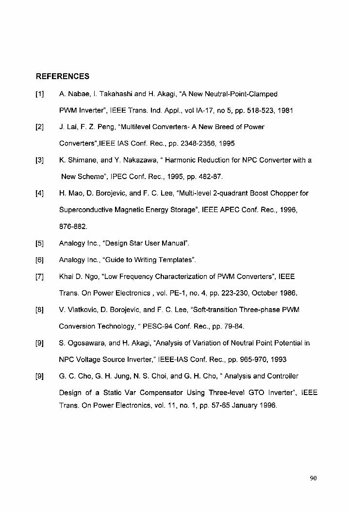
REFERENCES
(1]
[2]
[3]
[4]
[5]
[5]
[7]
[8]
[9]
[9]
A. Nabae, |. Takahashi and H. Akagi, “A New Neutral-Point-Clamped
PWM Inverter’, IEEE Trans. Ind. Appl., vol JA-17, no 5, pp. 518-523, 1981
J. Lai, F. Z. Peng, “Multilevel Converters- A New Breed of Power
Converters” IEEE IAS Conf. Rec., pp. 2348-2356, 1995
K. Shimane, and Y. Nakazawa, “ Harmonic Reduction for NPC Converter with a
New Scheme’, IPEC Conf. Rec., 1995, pp. 482-87.
H. Mao, D. Borojevic, and F. C. Lee, “Multi-level 2-quadrant Boost Chopper for
Superconductive Magnetic Energy Storage’, IEEE APEC Conf. Rec., 1996,
876-882.
Analogy Inc., “Design Star User Manual”.
Analogy Inc., “Guide to Writing Templates’.
Khai D. Ngo, “Low Frequency Characterization of PWM Converters”, IEEE
Trans. On Power Electronics , vol. PE-1, no. 4, pp. 223-230, October 1986.
V. Viatkovic, D. Borojevic, and F. C. Lee, “Soft-transition Three-phase PWM
Conversion Technology, “ PESC-94 Conf. Rec., pp. 79-84.
S. Ogosawara, and H. Akagi, “Analysis of Variation of Neutral Point Potential in
NPC Voltage Source Inverter,” IEEE-IAS Conf. Rec., pp. 965-970, 1993
G. C. Cho, G. H. Jung, N. S. Choi, and G. H. Cho, “ Analysis and Controller
Design of a Static Var Compensator Using Three-level GTO Inverter’, IEEE
Trans. On Power Electronics, vol. 11, no. 1, pp. 57-65 January 1996.
90

[10]
[11]
[12]
[13]
Silva Hiti, “Modeling and Control of Three-phase PWM Converters,”, Ph.D.
Dissertation, Virginia Polytechnic Institute and State University, Blacksburg,
VA, 1995.
J. Bordonau, M. Cosan, D. Borojevic, H. Mao, and F. C. Lee, “A State-space
Model For The Comprehensive Dynamic Analysis of Three-level Voltage-source
Inverters”, IEEE, PESC Conf. Rec. 1997, pp. 942-948.
J. Xu, “Modeling of Switching dc-dc Converters by Time-averaging Equivalent
Circuit Approach,” Int. J. Electronics, vol. 74 no. 3, 1993
Evaluation version of PSPICE 7.1, MicroSim DesignLab.
91

Vita
Muhammet Cosan was born in Kocaeli, Turkey in 1971. He received his
Bachelor of Science degree with honors in electrical engineering from Istanbul
Technical University, Istanbul, Turkey, in 1992.
He joined Virginia Power Electronics Center (VPEC) in the spring of 1995
as a graduate research assistant. He was involved in research at VPEC in the
areas of space vector modulation techniques, modeling and control of switching
power converters. His area of interest includes soft switching techniques, multi-
level converters and high-power applications. He is currently a design engineer
with York International Corp., York, PA.
\ n \ ?
* nr > lw aedh = - t a - oy , soa fe acl | Ce WA
i
92