verilog digital system_design (navabi testbend va rtl)
TRANSCRIPT
Verilog DigitalSystem Design
RT Level Synthesis,Testbench and Verification
Zainalabedin Navabi, Ph.D.Professor of Electrical and Computer Engineering
Northeastern UniversityBoston, Massachusetts
Second Edition
McGraw-HillNew York Chicago San Francisco Lisbon London Madrid
Mexico City Milan New Delhi San Juan Seoul Singapore Sydney Toronto

Copyright © 2006 by The McGraw-Hill Publishing Companies, Inc. All rights reserved. Manufacturedin the United States of America. Except as permitted under the United States Copyright Act of 1976,no part of this publication may be reproduced or distributed in any form or by any means, or stored ina database or retrieval system, without the prior written permission of the publisher.
0-07-158892-2
The material in this eBook also appears in the print version of this title: 0-07-144564-1.
All trademarks are trademarks of their respective owners. Rather than put a trademark symbol afterevery occurrence of a trademarked name, we use names in an editorial fashion only, and to the benefit of the trademark owner, with no intention of infringement of the trademark. Where such designations appear in this book, they have been printed with initial caps.
McGraw-Hill eBooks are available at special quantity discounts to use as premiums and sales promotions, or for use in corporate training programs. For more information, please contact GeorgeHoare, Special Sales, at [email protected] or (212) 904-4069.
TERMS OF USE
This is a copyrighted work and The McGraw-Hill Companies, Inc. (“McGraw-Hill”) and its licensorsreserve all rights in and to the work. Use of this work is subject to these terms. Except as permittedunder the Copyright Act of 1976 and the right to store and retrieve one copy of the work, you may notdecompile, disassemble, reverse engineer, reproduce, modify, create derivative works based upon,transmit, distribute, disseminate, sell, publish or sublicense the work or any part of it without McGraw-Hill’s prior consent. You may use the work for your own noncommercial and personal use;any other use of the work is strictly prohibited. Your right to use the work may be terminated if youfail to comply with these terms.
THE WORK IS PROVIDED “AS IS.” McGRAW-HILL AND ITS LICENSORS MAKE NO GUARANTEES OR WARRANTIES AS TO THE ACCURACY, ADEQUACY OR COMPLETE-NESS OF OR RESULTS TO BE OBTAINED FROM USING THE WORK, INCLUDING ANYINFORMATION THAT CAN BE ACCESSED THROUGH THE WORK VIA HYPERLINK OROTHERWISE, AND EXPRESSLY DISCLAIM ANY WARRANTY, EXPRESS OR IMPLIED,INCLUDING BUT NOT LIMITED TO IMPLIED WARRANTIES OF MERCHANTABILITY ORFITNESS FOR A PARTICULAR PURPOSE. McGraw-Hill and its licensors do not warrant or guarantee that the functions contained in the work will meet your requirements or that its operationwill be uninterrupted or error free. Neither McGraw-Hill nor its licensors shall be liable to you or anyone else for any inaccuracy, error or omission, regardless of cause, in the work or for any damagesresulting therefrom. McGraw-Hill has no responsibility for the content of any information accessedthrough the work. Under no circumstances shall McGraw-Hill and/or its licensors be liable for anyindirect, incidental, special, punitive, consequential or similar damages that result from the use of orinability to use the work, even if any of them has been advised of the possibility of such damages. Thislimitation of liability shall apply to any claim or cause whatsoever whether such claim or cause arisesin contract, tort or otherwise.
DOI: 10.1036/0071445641

We hope you enjoy thisMcGraw-Hill eBook! If
you’d like more information about this book,its author, or related books and websites,please click here.
Professional
Want to learn more?

To my mother, Sadri Kheradmand (Navabi),who inspired me to pursue a life of scienceand engineering.

This page intentionally left blank
Contents
Preface xiii
Chapter 1. Digital System Design Automation with Verilog 1
1.1 Digital Design Flow 21.1.1 Design entry 31.1.2 Testbench in Verilog 41.1.3 Design validation 41.1.4 Compilation and synthesis 71.1.5 Postsynthesis simulation 101.1.6 Timing analysis 101.1.7 Hardware generation 10
1.2 Verilog HDL 101.2.1 Verilog evolution 111.2.2 Verilog attributes 111.2.3 The Verilog language 13
1.3 Summary 13Problems 13Suggested Reading 14
Chapter 2. Register Transfer Level Design with Verilog 15
2.1 RT Level Design 152.1.1 Control/data partitioning 162.1.2 Data part 162.1.3 Control part 17
2.2 Elements of Verilog 182.2.1 Hardware modules 182.2.2 Primitive instantiations 192.2.3 Assign statements 202.2.4 Condition expression 202.2.5 Procedural blocks 202.2.6 Module instantiations 21
2.3 Component Description in Verilog 22
v
For more information about this title, click here
2.3.1 Data components 222.3.2 Controllers 29
2.4 Testbenches 332.4.1 A simple tester 332.4.2 Tasks and functions 34
2.5 Summary 34Problems 35Suggested Reading 35
Chapter 3. Verilog Language Concepts 37
3.1 Characterizing Hardware Languages 373.1.1 Timing 373.1.2 Concurrency 393.1.3 Timing and concurrency example 40
3.2 Module Basics 413.2.1 Code format 413.2.2 Logic value system 413.2.3 Wires and variables 423.2.4 Modules 423.2.5 Module ports 433.2.6 Names 433.2.7 Numbers 443.2.8 Arrays 463.2.9 Verilog operators 48
3.2.10 Verilog data types 543.2.11 Array indexing 58
3.3 Verilog Simulation Model 593.3.1 Continuous assignments 613.3.2 Procedural assignments 65
3.4 Compiler Directives 713.4.1 `timescale 713.4.2 `default-nettype 713.4.3 `include 713.4.4 `define 713.4.5 `ifdef, `else, `endif 723.4.6 `unconnected-drive 723.4.7 `celldefine, `endcelldefine 723.4.8 `resetall 72
3.5 System Tasks and Functions 723.5.1 Display tasks 733.5.2 File I/O tasks 733.5.3 Timescale tasks 743.5.4 Simulation control tasks 743.5.5 Timing check tasks 743.5.6 PLA modeling tasks 743.5.7 Conversion functions for reals 753.5.8 Other tasks and functions 75
3.6 Summary 76Problems 76Suggested Reading 80
vi Contents
Chapter 4. Combinational Circuit Description 81
4.1 Module Wires 814.1.1 Ports 814.1.2 Interconnections 824.1.3 Wire values and timing 824.1.4 A simple testbench 84
4.2 Gate Level Logic 854.2.1 Gate primitives 854.2.2 User defined primitives 874.2.3 Delay formats 884.2.4 Module parameters 90
4.3 Hierarchical Structures 934.3.1 Simple hierarchies 934.3.2 Vector declarations 954.3.3 Iterative structures 964.3.4 Module path delay 99
4.4 Describing Expressions with Assign Statements 1024.4.1 Bitwise operators 1024.4.2 Concatenation operators 1044.4.3 Vector operations 1044.4.4 Conditional operation 1054.4.5 Arithmetic expressions in assignments 1084.4.6 Functions in expressions 1094.4.7 Bus structures 1104.4.8 Net declaration assignment 111
4.5 Behavioral Combinational Descriptions 1124.5.1 Simple procedural blocks 1134.5.2 Timing control 1134.5.3 Intra-assignment delay 1164.5.4 Blocking and nonblocking assignments 1164.5.5 Procedural if-else 1184.5.6 Procedural case statement 1204.5.7 Procedural for statement 1224.5.8 Procedural while loop 1234.5.9 A multilevel description 124
4.6 Combinational Synthesis 1254.6.1 Gate level synthesis 1274.6.2 Synthesizing continuous assignments 1284.6.3 Behavioral synthesis 1294.6.4 Mixed synthesis 132
4.7 Summary 132Problems 132Suggested Reading 134
Chapter 5. Sequential Circuit Description 135
5.1 Sequential Models 1355.1.1 Feedback model 1365.1.2 Capacitive model 1365.1.3 Implicit model 136
Contents vii
5.2 Basic Memory Components 1375.2.1 Gate level primitives 1375.2.2 User defined sequential primitives 1395.2.3 Memory elements using assignments 1405.2.4 Behavioral memory elements 1425.2.5 Flip-Flop timing 1495.2.6 Memory vectors and arrays 151
5.3 Functional Registers 1575.3.1 Shift registers 1575.3.2 Counters 1615.3.3 LFSR and MISR 1635.3.4 Stacks and queues 167
5.4 State Machine Coding 1715.4.1 Moore machines 1715.4.2 Mealy machines 1745.4.3 Huffman coding style 1765.4.4 A more modular style 1805.4.5 A ROM based controller 181
5.5 Sequential Synthesis 1815.5.1 Latch models 1835.5.2 Flip-flop models 1845.5.3 Memory initialization 1855.5.4 General sequential circuit synthesis 186
5.6 Summary 186Problems 187Suggested Reading 189
Chapter 6. Component Test and Verification 191
6.1 Testbench 1916.1.1 Combinational circuit testing 1926.1.2 Sequential circuit testing 194
6.2 Testbench Techniques 1956.2.1 Test data 1966.2.2 Simulation control 1976.2.3 Limiting data sets 1986.2.4 Applying synchronized data 1996.2.5 Synchronized display of results 2006.2.6 An interactive testbench 2016.2.7 Random time intervals 2046.2.8 Buffered data application 205
6.3 Design Verification 206
6.4 Assertion Verification 2076.4.1 Assertion verification benefits 2086.4.2 Open verification library 2086.4.3 Using assertion monitors 2096.4.4 Assertion templates 216
6.5 Text Based Testbenches 219
6.6 Summary 220Problems 220Suggested Reading 221
viii Contents
Chapter 7. Detailed Modeling 223
7.1 Switch Level Modeling 2237.1.1 Switch level primitives 2247.1.2 The basic switch 2257.1.3 CMOS gates 2267.1.4 Pass gate logic 2307.1.5 Switch level memory elements 234
7.2 Strength Modeling 2417.2.1 Strength values 2427.2.2 Strength used in resolution 2447.2.3 Strength reduction 247
7.3 Summary 250Problems 250Suggested Reading 251
Chapter 8. RT Level Design and Test 253
8.1 Sequential Multiplier 2538.1.1 Shift-and-add multiplication process 2548.1.2 Sequential multiplier design 2568.1.3 Multiplier testing 261
8.2 von Neumann Computer Model 2658.2.1 Processor and memory model 2658.2.2 Processor model specification 2668.2.3 Designing the adding CPU 2678.2.4 Design of datapath 2688.2.5 Control part design 2698.2.6 Adding CPU Verilog description 2708.2.7 Testing adding CPU 275
8.3 CPU Design and Test 2818.3.1 Details of processor functionality 2818.3.2 SAYEH datapath 2838.3.3 SAYEH Verilog description 2878.3.4 SAYEH top-level testbench 2988.3.5 Sorting test program 3048.3.6 SAYEH hardware realization 304
8.4 Summary 306Problems 306Suggested Reading 307
Appendix A. List of Keywords 309
Appendix B. Frequently Used System Tasks and Functions 311
Appendix C. Compiler Directives 319
Appendix D. Verilog Formal Syntax Definition 321
Appendix E. Verilog Assertion Monitors 345
Index 375
Contents ix

This page intentionally left blank
Preface
This book is on the IEEE Standard Hardware Description Languagebased on the Verilog® Hardware Description Language (Verilog HDL),IEEE Std 1364–2001. The intended audiences are engineers involved invarious aspects of digital systems design and manufacturing and studentswith the basic knowledge of digital system design. The emphasis of thebook is on using Verilog HDL for the design, verification, and synthesis ofdigital systems. We will discuss Register Transfer (RT) level digital systemdesign, and discuss how Verilog can be used in this design flow.
In the last few years RT level design of digital systems has gonethrough significant changes. Beyond simulation and synthesis that arenow part of any RTL design process, we are looking at testbench gen-eration and automatic verification tools. As with any book on Verilog,this book covers digital design and Verilog for simulation and synthe-sis. However, to ready design engineers for designing, testing, and ver-ifying large digital system designs, the book contains material fortestbench development and verification. The subjects of testbench andverification are introduced in Chapter 1. Chapter 2 onwards we con-centrate on Verilog for design and synthesis. This will teach the read-ers efficient Verilog coding techniques for describing actual hardwarecomponents. When all of Verilog from a design point of view is pre-sented, we turn our attention to test and verification. Chapter 6 coverstestbench development techniques and use of assertion verification mon-itors for better analysis of a design. Toward the end of the book we puttogether our coding techniques for synthesis and testbench develop-ment, and present several RT level designs from design specification toverification.
Embedded in the presentation of the language, the book provides areview of digital system design and computer architecture concepts.This review is useful for relearning these concepts as demanded by newdesign methodologies and hardware description language based designtools. For practicing engineers the flow of the book, which starts from
xi
Copyright © 2006 by The McGraw-Hill Publishing Companies, Inc. Click here for terms of use.
introductory material and advances into complex digital design con-cepts, provides a self-sufficient learning tool. The material is suitablefor an upper division undergraduate or a first year graduate course. Fora one-semester course on the Verilog HDL language and its use in a dig-ital system design environment, the book can be used in its entirety. Thebook can also be used as a supplement for graduate and undergraduatedigital system design and computer organization courses.
Overview of the Chapters
Chapter overviews are presented below. This material is intended to helpa reader concentrate on parts of the book that he or she finds suit ableto his or her needs best. Chapters 1 and 2 are introductory, and containmaterial with which many readers may already be familiar. It is, how-ever, recommended that these chapters not be completely omitted, evenby experienced readers. The Verilog language is presented in Chapter 3and includes the details of language syntax and semantics. The next twochapters (4 and 5) concentrate on Verilog for describing hardware froma design point of view. This is followed by a chapter on testing. Together,Chapters 4, 5, and 6 cover use of Verilog for design and test of digitalsystems. Chapter 7, which is on detailed modeling, is useful for VLSIdesigners. The last example in Chapter 8 is a complete processor thatis modeled for synthesis and a complete testbench is developed for it.
Chapter 1 gives an overview of digital design process and the use of hard-ware description languages in this process. Simulation, synthesis, formalverification, and assertion verification are discussed in this chapter.
Chapter 2 shows various ways hardware components can be describedin Verilog. The purpose of this chapter is to give the reader a generaloverview of the Verilog language.
Chapter 3 discusses the complete Verilog language structure. Thefocus of the chapter is more on the linguistic issues and not on model-ing hardware components. A general understanding of the language isnecessary before it can be used for hardware modeling. Writing Verilogfor describing hardware is discussed in the chapters that follow thischapter.
Chapter 4 starts with gates and ends with high-level Verilog con-structs for description of combinational circuits. Concurrency and timingwill be discussed in the examples of this chapter. Except for specifica-tion of timing parameters, codes discussed in this chapter are synthe-sizable. A section in this chapter presents rules for writing synthesizablecombinational circuits.
Chapter 5 discusses modeling and description of sequential circuitsin Verilog. The chapter begins with models of memory and shows howthey can be specified in Verilog. Registers, counters, and state machines
xii Preface
are discussed in this chapter. A section in this chapter presents rules forwriting synthesizable sequential circuits.
Chapter 6 is on writing testbenches in Verilog. The previous twochapters discussed Verilog from a hardware design point of view, andthis chapter shows how components described as such can be tested.We talk about data generation, response analysis, and assertion veri-fication.
Chapter 7 covers switch level modeling and detailed representationof signals in Verilog. This material is geared more for those using Verilogas a modeling language and less for designers. VLSI structures can bedescribed by Verilog constructs discussed here.
Chapter 8 shows complete RTL design flow, from problem specifica-tion to test. We show several complete examples that take advantage ofmaterial of Chapters 4, 5, and 6 for description, simulation, verification,and synthesis of digital systems. Examples in this chapter take advan-tage of text IO facilities of Verilog for storing test data and circuitresponses.
Appendix Acontains Verilog keywords. Appendix B lists commonly usedsystem tasks and briefly describes each task. Appendix C lists Verilogcompiler directives and explains their use. Appendix D presents thestandard IEEE Verilog HDL syntax. Language constructs terminalsand nonterminals are presented here in a formal grammar representa-tion. Appendix E presents the OVL assertion monitors. After a briefdescription of each assertion monitor its parameters and argumentsare explained.
Suggested Reading Flow
The book teaches the Verilog language for RT level design, simulation,verification, and synthesis of digital systems. For a complete compre-hension of these issues, or for a complete one-semester graduate course,the book is recommended in its entirety. However, for specific needsand requirements or for an undergraduate course on automated designmethodologies, parts of the book can also be used. The following para-graphs present several such uses.
For a hardware designer interested in learning about synthesis,Chapters 4 and 5 are the most important ones. For such users, Chapter 3can be used as a reference, and Chapter 6, which is on testbench devel-opment, can be studied as needed. When the designer is ready to considercomplete systems, Chapter 8 is recommended.
Chapter 2 is introductory and provides an overview of the language.For a student using Verilog in a lower-level undergraduate course, thischapter is a good starting point for learning the language. More com-plex parts of the language can then be learned as needed.
Preface xiii
Chapter 8 can be used for learning computer organization concepts andthe use of Verilog in description of these structures. Readers familiar withVerilog can use their knowledge to learn the inter-workings of CPU struc-tures, instruction execution, and testing large systems.
The flow of the book is such that it provides a complete knowledge ofVerilog using the same flow as that used in teaching hardware designin most 4-year Computer Engineering programs. The following outlinesindicate various applications of the book for beginners, undergraduatestudents, graduate students, designer engineers, modelers, and systemdesigners.
1. General introduction for a lower-level undergraduate course or anentry level design engineer:� Chapters 1–2. Design flow and Verilog overview� Chapters 4–5. Combinational and sequential circuits for synthesis
2. Advanced logic design for a senior-level course or an advanced designengineer with some familiarity with design flow and Verilog syntax:� Chapters 1–2. A review of Verilog-based design� Chapter 3. Language semantics and constructs� Chapters 4–5. Combinational and sequential circuits for synthesis� Chapter 6. Test methods
3. Advanced system design for a senior-level course or an advancedsystem design engineer with some familiarity with design flow andVerilog syntax:� Chapters 1–2. A review of Verilog-based design� Chapter 3. Use as reference as needed� Chapters 4–5. Combinational and sequential circuits for synthesis� Chapter 6. Test methods� Chapter 8. Top-down design of systems
4. Advanced modeling and system design for a graduate-level course oran advanced VLSI design engineer:� Chapters 1–2. A review of Verilog-based design� Chapter 3. Use as reference as needed� Chapters 4–5. Combinational and sequential circuits for synthesis� Chapter 6. Test methods� Chapter 7. Switch level and CMOS modeling� Chapter 8. Top-down design of systems
5. Parallel with undergraduate Computer Engineering program:� Use Chapters 1 and 2 early in a digital logic design course� Use Chapters 4 and 5 in a digital logic design course in parallel with
discussion of combinational and sequential circuits� Use Chapter 6 in a technical elective design course
xiv Preface
� Use Chapter 7 in the senior-level VLSI course� Use Chapter 8 in the Junior or Sophomore computer architecture
course
Code Examples
Among many tasks involved in the preparation of the manuscript, fora book describing a language that is as example oriented as this book,selecting appropriate set of examples and presenting them to the readerare of special importance. For every design example presented in thisbook, a testbench is generated and the design has been tested. Withevery example, there is a logic design concept and there are severalVerilog constructs and features that are covered. The set of examples ischosen to present the complete Verilog language for synthesis. Theseexamples start with using simple Verilog constructs and progressivelymove into more complex ones. Parallel with the flow of language con-structs, the book starts with using simple logic design concepts, such asusing basic gates for combinational circuits, and moves into advancedlogic design concepts such as queues and processors.
The CD accompanying this book includes simulation, synthesis, anddevice programming software tools. Verilog description of the examplesof this book and their testbenches are also included on this CD. For theinstructors using this book in an educational setting, solutions for theend of chapter problems and Power Point lecture slides can be obtainedfrom the author or the publisher.
Acknowledgments
Guidelines, comments, reviews, and support of many people helped thedevelopment of this book, and the author wishes to thank them. Thestyle used for presenting the material is based on simple examples thatcover a certain topic and discussing the issues that the example covers.As with the other books that I have written, I have used guidelines andwriting philosophy of the late Professor Fredrick J. Hill of the Universityof Arizona, with whom I worked many years as a student and a researchassociate. My students and colleagues were particularly helpful in thedevelopment of this book. In the past 15 years, my students at theUniversity of Tehran, Northeastern University and National TechnologicalUniversity have been very helpful in bringing up ideas for more illustra-tive examples. Many examples come from exam and homework ques-tions that these students had to struggle with.
At the start of this writing project, my associate, Ms. Fatemeh Asgariassumed responsibility for managing the preparation of the manuscript.Organizing the efforts for manuscript preparation, managing the timing
Preface xv

of this task with my many other tasks has been a very challenging taskfor her. Her crystal ball always told the truth about how bad I would missmy deadlines. Students at the University of Tehran, Armin Alaghi,Najmeh Fakhraie, Amirali Ghofrani, Aida Hasani, and Mahsan Rofouei,were very helpful in completion of this project. They helped reviewingthe manuscript, coding, preparing the artwork, and suggesting ways ofimproving the flow of the book for different levels of audiences.
Most of all, I thank my wife, Irma Navabi, for help encouragement andunderstanding of my working habits. Such an intensive work could notbe done if I did not have support of my wife and my two sons, Aarashand Arvand. I thank them for this and other scientific achievements Ihave had.
Zainalabedin Navabi, Ph.D.Boston, Massachusetts
xvi Preface
Chapter
1Digital System Design
Automation with Verilog
As the size and complexity of digital systems increase, more computer-aided design (CAD) tools are introduced into the hardware designprocess. Early simulation and primitive hardware generation tools havegiven way to sophisticated design entry, verification, high-level syn-thesis, formal verification, and automatic hardware generation anddevice programming tools. Growth of design automation tools is largelydue to hardware description languages (HDLs) and design methodolo-gies that are based on these languages. Based on HDLs, new digitalsystem CAD tools have been developed and are now widely used byhardware designers. At the same time research for finding better andmore abstract hardware languages continues. One of the most widelyused HDLs is the Verilog HDL. Because of its wide acceptance in digi-tal design industry, Verilog has become a must-know for design engi-neers and students in computer-hardware-related fields.
This chapter presents tools and environments that are based onVerilog and are available to a hardware designer for automating his orher design process, and hence improving the final product’s time tomarket. We discuss steps involved in taking a hierarchical, high-leveldesign from a Verilog description of the design to its implementation inhardware. Processes and terminologies are illustrated here. We discussavailable electronic design automation (EDA) tools that are based onVerilog, and talk about their role in an automated design environment.The last section of this chapter discusses some of the properties ofVerilog that make this language a good choice for designers and mod-elers of hardware.
1
Copyright © 2006 by The McGraw-Hill Publishing Companies, Inc. Click here for terms of use.
1.1 Digital Design Flow
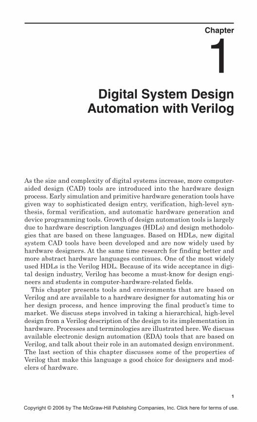
For the design of a digital system using an automated design environ-ment, the design flow begins with specification of the design at variouslevels of abstraction and ends with generating netlist for an applicationspecific integrated circuits (ASIC), layout for a custom IC, or a programfor a programmable logic devices (PLD). Figure 1.1 shows steps involvedin this design flow.
In the design entry phase, a design is specified as a mixture of behav-ioral Verilog code, instantiation of Verilog modules, and bus and wire assign-ments. A design engineer is also responsible for generating testbenches
2 Chapter One
Compilation and Synthesis
SynthesisAnalysis Routing and placement
Y = a & d & ww = a & b | c
Post-synthesis Simulation
Timing Analysis
1.6 ns2 ns
Behavioral Simulation Assertion Verification Formal Verification
Pass/Fail ReportProperty CoverageCounter Examples
Comp1 U1 (. . .);Comp2 U2 (. . .);. . .Compn Un (. . .);
always (posedge clk)begin . . . end
if (. . .) bus = w;else . . .
module design (. . .); assign . . . always . . . compi (. . .)endmodule
Testbench in Verilog
Device Programming ASIC Netlist Custom IC Layout
EDIFor other netlists1010...
module testbench (); generate data; process data;endmodule
Violation Report;Time of Violation;Monitor Coverage
C++ Classes,Language Representation
Design Entry in Verilog
Figure 1.1 FPLD Design Flow
for his or her design for verification of the design and later for verify-ing the synthesis output. Design verification can be done by simulation,assertion verification, formal verification, or a mix of all three. After per-forming this design validation phase (this is called the presynthesisverification), this design is taken through the synthesis process to trans-late it into actual hardware of a target device. Here, target device refersto the specific field programmable logic device (FPLD) that is being pro-grammed, the ASIC that is being manufactured by an outside source,or the custom IC that is being fabricated. After the synthesis process andbefore the actual hardware is generated, another simulation, which isreferred to as postsynthesis simulation, is done. This simulation can takeadvantage of the same testbench generated for the Verilog model of thesystem before it is synthesized. This way, the behavioral model of thedesign and its hardware model are tested with the same data. The dif-ference between pre- and postsynthesis simulations is in the level ofdetails obtained from each simulation.
The sections that follow elaborate on each of the blocks shown in Fig. 1.1.Most Verilog based EDAenvironments provide blocks shown in this figure.
1.1.1 Design entry
The first step in the design of a digital system is the design entry phase.In this phase, the design is described in Verilog in a top-down hierarchicalfashion. A complete design may consist of components at the gate ortransistor level, behavioral parts describing high-level functionality of ahardware module, or components described by their bussing structure.
Because high-level Verilog designs are usually described at the level thatspecifies system registers and transfer of data between registers throughbusses, this level of system description is referred to as register transferlevel (RTL). Acomplete design described as such has a clear hardware cor-respondence. Verilog constructs used in an RT level design are proceduralstatements, continuous assignments, and instantiation statements.
Verilog procedural statements are used for high-level behavioraldescriptions. A system or a component is described in a proceduralfashion similar to the way processes are described in a software language.For example, we can describe a component by checking its input condi-tions, setting flags, waiting for events to occur, monitoring handshakingsignals, and issuing outputs. Describing a system procedurally, Verilogif-else, case and other software-language-like constructs can be used.
Verilog continuous assignments are statements for representing logicblocks, bus assignments, and bus and input/output interconnect speci-fications. Combined with boolean and conditional operations, these lan-guage constructs can be used for describing components and systems interms of their register and bus assignments.
Digital System Design Automation with Verilog 3
Verilog instantiation statements are for using lower-level componentsin an upper-level design. Instead of describing behavior, functionality,or bussing of a system, we can describe a system in Verilog in terms ofits lower-level components. These subcomponents can be as small as agate or a transistor, or as large as a complete processor.
1.1.2 Testbench in Verilog
A system designed in Verilog must be simulated and tested for function-ality before it is turned into hardware. In this simulation pass, designerrors and incompatibility of components used in the design can bedetected. Simulating a design requires generation of test data and obser-vation of simulation results. This process can be done by use of a Verilogmodule that is referred to as a testbench. A Verilog testbench uses high-level constructs of this language for data generation, response monitor-ing, and even handshaking with the design. Inside the testbench, thedesign that is being simulated is instantiated. The testbench together withthe design forms a simulation model used by a Verilog simulation engine.
1.1.3 Design validation
An important task in any digital design is design validation. Design val-idation is the process that a designer checks his or her design for anydesign flaws that may have occurred in the design process. A design flawcan happen due to ambiguous problem specifications, designer errors,or incorrect use of parts in the design. Design validation can be done bysimulation, assertion verification, or formal verification.
1.1.3.1 Simulation. Simulation for design validation is done before adesign is synthesized. This simulation pass is also referred to as behav-ioral, RT level, or presynthesis simulation. At the RT level a designincludes clock-level timing but no gate and wire delays are included.Simulation at this level is accurate to the clock level. Timing of RT-levelsimulation is at the clock level and does not usually consider hazards,glitches, race conditions, setup and hold violations, and other detailedtiming issues. The advantage of this simulation is its speed comparedwith simulations at the gate or transistor levels.
Simulation of a design requires test data, and usually Verilog simu-lation environments provide various methods for application of thesedata to the design being tested. Test data can be generated graphicallyusing waveform editors, or through a testbench. Figure 1.2 shows twoalternatives for defining test input data for a simulation engine. Outputsof simulators are in the form of waveforms (for visual inspection) and textfor large designs for machine processing.
4 Chapter One
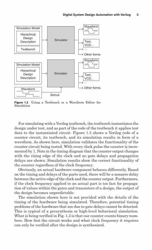
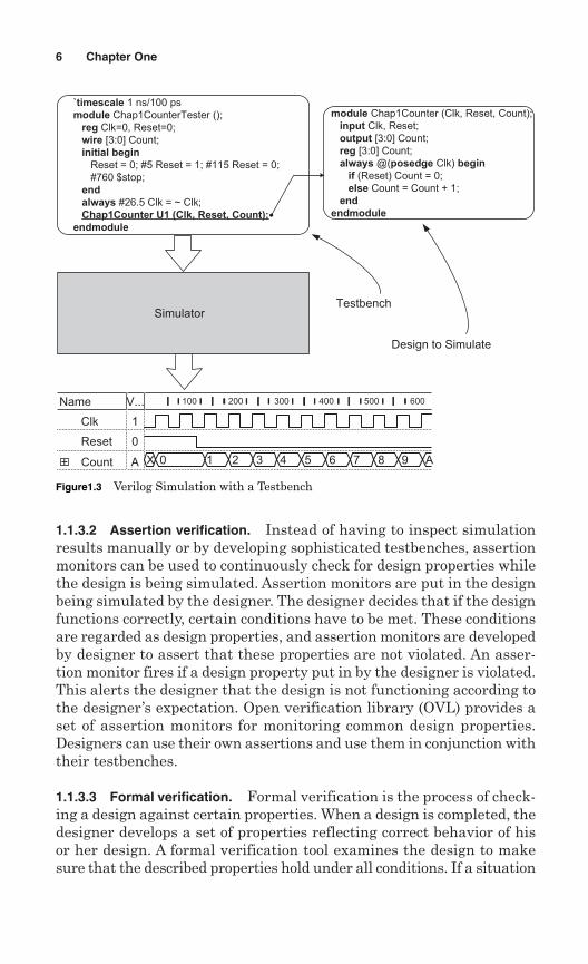
For simulating with a Verilog testbench, the testbench instantiates thedesign under test, and as part of the code of the testbench it applies testdata to the instantiated circuit. Figure 1.3 shows a Verilog code of acounter circuit, its testbench, and its simulation results in form of awaveform. As shown here, simulation validates the functionality of thecounter circuit being tested. With every clock pulse the counter is incre-mented by 1. Note in the timing diagram that the counter output changeswith the rising edge of the clock and no gate delays and propagationdelays are shown. Simulation results show the correct functionality ofthe counter regardless of the clock frequency.
Obviously, an actual hardware component behaves differently. Basedon the timing and delays of the parts used, there will be a nonzero delaybetween the active edge of the clock and the counter output. Furthermore,if the clock frequency applied to an actual part is too fast for propaga-tion of values within the gates and transistors of a design, the output ofthe design becomes unpredictable.
The simulation shown here is not provided with the details of thetiming of the hardware being simulated. Therefore, potential timingproblems of the hardware that are due to gate delays cannot be detected.This is typical of a presynthesis or high-level behavioral simulation.What is being verified in Fig. 1.3 is that our counter counts binary num-bers. How fast the circuit works and what clock frequency it requirescan only be verified after the design is synthesized.
Digital System Design Automation with Verilog 5
Testbench
Text,VCD...
Waveform
Other forms
Simulation Model
HierachicalDesign
Description
Simulator
...
Simulation Model
Text,VCD...
Waveform
Other forms
...
Stimuli
HierachicalDesign
Description
Simulator
Waveform
Figure 1.2 Using a Testbench or a Waveform Editor forSimulation
1.1.3.2 Assertion verification. Instead of having to inspect simulationresults manually or by developing sophisticated testbenches, assertionmonitors can be used to continuously check for design properties whilethe design is being simulated. Assertion monitors are put in the designbeing simulated by the designer. The designer decides that if the designfunctions correctly, certain conditions have to be met. These conditionsare regarded as design properties, and assertion monitors are developedby designer to assert that these properties are not violated. An asser-tion monitor fires if a design property put in by the designer is violated.This alerts the designer that the design is not functioning according tothe designer’s expectation. Open verification library (OVL) provides aset of assertion monitors for monitoring common design properties.Designers can use their own assertions and use them in conjunction withtheir testbenches.
1.1.3.3 Formal verification. Formal verification is the process of check-ing a design against certain properties. When a design is completed, thedesigner develops a set of properties reflecting correct behavior of hisor her design. A formal verification tool examines the design to makesure that the described properties hold under all conditions. If a situation
6 Chapter One
`timescale 1 ns/100 psmodule Chap1CounterTester ();
reg Clk=0, Reset=0;wire [3:0] Count;
initial begin
Reset = 0; #5 Reset = 1; #115 Reset = 0; #760 $stop; end
always #26.5 Clk = ~ Clk;Chap1Counter U1 (Clk, Reset, Count);
endmodule
module Chap1Counter (Clk, Reset, Count); input Clk, Reset;output [3:0] Count;reg [3:0] Count;always @(posedge Clk) begin
if (Reset) Count = 0;else Count = Count + 1;
end
endmodule
SimulatorTestbench
Design to Simulate
Name V...
1
0Reset
Clk
ACount
100 200 300 400 500 600
+ X 0 1 2 3 4 5 6 7 8 9 A
Figure1.3 Verilog Simulation with a Testbench

is found that the property will not hold, the property is said to have beenviolated. Input conditions that make a property fail are regarded as theproperty’s counter examples. Property coverage indicates how much ofthe complete design is exercised by the property.
1.1.4 Compilation and synthesis
Synthesis is the process of automatic hardware generation from a designdescription that has an unambiguous hardware correspondence. AVerilog description for synthesis cannot include signal and gate leveltiming specifications, file handling, and other language constructs thatdo not translate to sequential or combinational logic equations.Furthermore, Verilog descriptions for synthesis must follow certainstyles of coding for combinational and sequential circuits. These stylesand their corresponding Verilog constructs are defined under Verilog forRTL synthesis.
In the design process, after a design is successfully entered and itspresynthesis simulation results have been verified by the designer, itmust be compiled to make it one step closer to an actual hardware onsilicon. This design phase requires specification of the hardware that thedesign is to be realized in. For example, we have to specify a specificASIC, or a field programmable gate array (FPGA) part as our “targethardware.” When the target hardware is specified, technology files ofthat hardware (ASIC, FPGA, or custom IC) with detailed timing andfunctional specification become available to the compilation process.The compilation process, translates various parts of the design to anintermediate format (analysis phase), links all parts together, generatesthe corresponding logic (synthesis phase), places and routes compo-nents of the target hardware, and generates timing details.
Figure 1.4 shows the compilation process and a graphical represen-tation for each of the compilation phase outputs. As shown, the input ofthis phase is a hardware description that consists of various levels ofVerilog, and its output is a detailed hardware for programming anFPLDor manufacturing an ASIC.
1.1.4.1 Analysis. A complete design that is described in Verilog may con-sist of behavioral Verilog, bus and interconnection specifications, andwiring of other Verilog components. Before the complete design is turnedinto hardware, the design must be analyzed and a uniform format mustbe generated for all parts of the design. This phase also checks the syntaxand semantics of the input Verilog code.
1.1.4.2 Generic hardware generation. After obtaining a uniform pres-entation for all components of a design, the synthesis pass begins its
Digital System Design Automation with Verilog 7
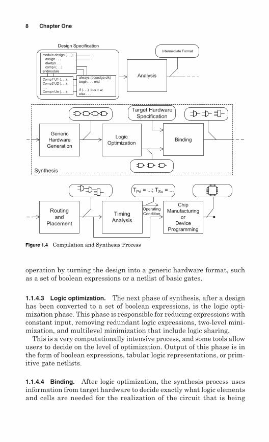
operation by turning the design into a generic hardware format, suchas a set of boolean expressions or a netlist of basic gates.
1.1.4.3 Logic optimization. The next phase of synthesis, after a designhas been converted to a set of boolean expressions, is the logic opti-mization phase. This phase is responsible for reducing expressions withconstant input, removing redundant logic expressions, two-level mini-mization, and multilevel minimization that include logic sharing.
This is a very computationally intensive process, and some tools allowusers to decide on the level of optimization. Output of this phase is inthe form of boolean expressions, tabular logic representations, or prim-itive gate netlists.
1.1.4.4 Binding. After logic optimization, the synthesis process usesinformation from target hardware to decide exactly what logic elementsand cells are needed for the realization of the circuit that is being
8 Chapter One
Design Specification
Comp1 U1 (. . .);Comp2 U2 (. . .);. . .Compn Un (. . .);
Analysis
LogicOptimization
Target HardwareSpecification
Intermediate Format
Synthesis
TPd = ...; TSu = ...
ChipManufacturing
orDevice
Programming
always (posedge clk)begin . . . end
if (. . .) bus = w;else . . .
module design (. . .);assign . . .always . . .compi (. . .)
endmodule
GenericHardware
GenerationBinding
OperatingCondition
Routingand
Placement
TimingAnalysis
Figure 1.4 Compilation and Synthesis Process
designed. This process is called binding and its output is specific to theFPLD, ASIC, or custom IC being used.
1.1.4.5 Routing and placement. The routing and placement phasedecides on the placement of cells of the target hardware. Wiring inputsand outputs of these cells through wiring channels and switching areasof the target hardware are determined by the routing and placementphase. The output of this phase is specific to the hardware being usedand can be used for programming an FPLD or manufacturing an ASIC.
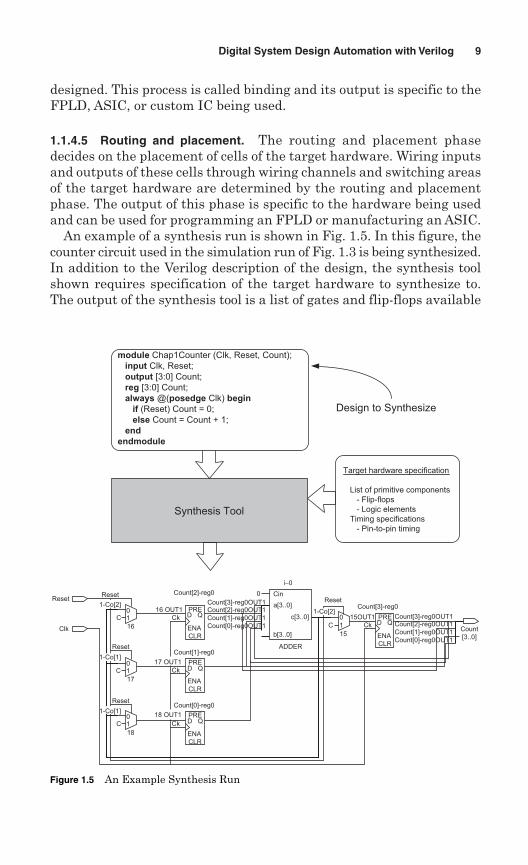
An example of a synthesis run is shown in Fig. 1.5. In this figure, thecounter circuit used in the simulation run of Fig. 1.3 is being synthesized.In addition to the Verilog description of the design, the synthesis toolshown requires specification of the target hardware to synthesize to.The output of the synthesis tool is a list of gates and flip-flops available
Digital System Design Automation with Verilog 9
module Chap1Counter (Clk, Reset, Count); input Clk, Reset;output [3:0] Count;reg [3:0] Count;always @(posedge Clk) begin
if (Reset) Count = 0;else Count = Count + 1;
end
endmodule
Synthesis Tool
Target hardware specification
List of primitive components - Flip-flops - Logic elementsTiming specifications - Pin-to-pin timing
Design to Synthesize
ResetReset
Reset
Reset
Clk
C01
C01
18
17
C01
16
16 OUT1
17 OUT1
18 OUT1
Ck
Ck
CkCk
D QPRE
ENACLR
D QPRE
ENACLR
D QPRE
ENACLR
D QPRE
ENACLR
Count[2]-reg0
Count[3]-reg0OUT1Count[2]-reg0OUT1Count[1]-reg0OUT1Count[0]-reg0OUT1
Count[3]-reg0OUT1
Count[3]-reg0
Count[2]-reg0OUT1Count[1]-reg0OUT1Count[0]-reg0OUT1
Count[1]-reg0
Count[0]-reg0
Count[3..0]
1-Co[2]
1-Co[1]
1-Co[1]
0 Cin
a[3..0]
b[3..0]
c[3..0]
i−0
ADDER
Reset
01C
1-Co[2]
15
15OUT1
Figure 1.5 An Example Synthesis Run
in the target hardware, and their interconnections. A graphical repre-sentation of this output that is automatically generated by the synthe-sis tool of Altera’s Quartus II is shown in Fig. 1.5.
1.1.5 Postsynthesis simulation
After synthesis is done, the synthesis tool generates a complete netlistof target hardware components and their timings. The details of gatesused for the implementation of the design are described in this netlist.The netlist also includes wiring delays and load effects on gates used inthe postsynthesis design. The netlist output is made available in vari-ous netlist formats including Verilog. Such a description can be simu-lated and its simulation is referred to postsynthesis simulation. Timingissues, determination of a proper clock frequency and race, and hazardconsiderations can only be checked by a postsynthesis simulation runafter a design is synthesized. As shown in Fig. 1.1, the same testbenchtesting the original Verilog design before synthesis can be used for post-synthesis simulation.
Due to delays of wires and gates, it is possible that the behavior of adesign as intended by the designer and its behavior after postsynthesissimulation are different. In this case, the designer must modify his orher design and try to avoid close timings and race situations.
1.1.6 Timing analysis
As shown in Fig. 1.1, as part of the compilation process, or in some toolsafter the compilation process, there is a timing analysis phase. Thisphase generates worst-case delays, clocking speed, delays from one gateto another, as well as required setup and hold times. Results of timinganalysis appear in tables and/or graphs. Designers use this informationto decide on their clocking speed and, in general, speed of their circuits.
1.1.7 Hardware generation
The last stage in an automated Verilog-based design is hardware gen-eration. This stage generates a netlist for ASIC manufacturing, a pro-gram for programming FPLDs, or layout of custom IC cells.
1.2 Verilog HDL
The previous section showed steps involved in taking an RT level designfrom a Verilog description to hardware implementation. This designprocess is only possible because Verilog is a language that can be under-stood by system designers, RT level designers, test engineers, simulators,synthesis tools, and machines. Because of this important role in design,
10 Chapter One
Verilog has become an IEEE standard. The standard is used by usersas well as tool developers.
1.2.1 Verilog evolution
Verilog was designed in early 1984 by Gateway Design Automation.Initially the original language was used as a simulation and verifica-tion tool. After the initial acceptance of this language by electronicindustry, a fault simulator, a timing analyzer, and later in 1987, a syn-thesis tool was developed based on this language. Gateway DesignAutomation and its Verilog-based tools were later acquired by CadenceDesign System. Since then, Cadence has been a strong force behindpopularizing the Verilog hardware description language.
In 1987 VHDL became an IEEE standard hardware description lan-guage. Because of its Department of Defense (DoD) support, VHDL wasadapted by the U.S. government for related projects and contracts. In aneffort for popularizing Verilog, in 1990, OVI (Open Verilog International)was formed and Verilog was placed in public domain. This created a newline of interest in Verilog for the users and EDA vendors.
In 1993, efforts for standardization of this language started. Verilogbecame the IEEE standard, IEEE Std. 1364-1995, in 1995. Already havingsimulation tools, synthesizers, fault simulation programs, timing ana-lyzers, and many of their design tools developed for Verilog, this stan-dardization helped further acceptance of Verilog in electronic designcommunities.
A new version of Verilog was approved by IEEE in 2001. This versionthat is referred to as Verilog-2001 is the present standard used by mostusers and tool developers. New features for external file access for readand write, library management, constructs for design configuration,higher abstraction level constructs, and constructs for specification ofiterative structures, are some of the features added to this version ofVerilog. Work on improving this standard continues in various IEEEsponsored study groups.
1.2.2 Verilog attributes
Verilog is a hardware description language for describing hardware fromtransistor level to behavioral. The language supports timing constructsfor switch level timing simulation and at the same time, it has featuresfor describing hardware at the abstract algorithmic level. A Verilogdescription may consist of a mix of modules at various abstraction levelswith different degrees of detail.
1.2.2.1 Switch level. Features of the language that make it ideal forswitch level modeling and simulation includes primitive unidirectional
Digital System Design Automation with Verilog 11
and bidirectional switches with parameters for delay and charge storage.Circuit delays may be modeled as propagation delay, rise and fall delay,and line delays. The charge storage feature at this level of abstractionin Verilog makes this language capable of describing dynamic compli-mentary metal oxide semicondutor (CMOS) and metal oxide semicon-ductor (MOS) circuits.
1.2.2.2 Gate level. Gate level primitives with predefined parametersprovide a convenient platform for netlist representation and gate levelsimulation. For more detailed and special purpose gate simulations,gate components may be defined at the behavioral level. Verilog also pro-vides utilities for defining primitives with special functionalities. Asimple 4-value logic system is used in Verilog for signal values. However,for more accurate logic modeling, Verilog signals also include 16 levelsof strength in addition to the four values.
1.2.2.3 Pin-to-pin delay. A utility for timing specification of componentsat the input/output level is provided in Verilog. This utility can be usedfor back annotation of timing information in original predesigned descrip-tions. Moreover, the pin-to-pin language facility enables modelers to fine-tune timing behavior of their models based on physical implementations.
1.2.2.4 Bussing specifications. Bus and register modeling utilities areprovided in Verilog. For various bus structures, Verilog supports pre-defined wire and bus resolution functions using its 4-value logic valuesystem. Combination of bus logic and resolution-functions enable mod-eling of most physical bus types. For register modeling, high-level clockrepresentation and timing-control constructs can be used for represen-tation of registers with various clocking and resetting schemes.
1.2.2.5 Behavioral level. Procedural blocks of Verilog enable algorith-mic representations of hardware structures. Constructs similar to thosein software programming languages are provided for describing hard-ware at this level.
1.2.2.6 System utilities. System tasks in Verilog provide designers withtools for testbench generation, file access for read and write, data han-dling, data generation, and special hardware modeling. System utilitiesfor reading memory and programmable logic array (PLA) images pro-vide convenient ways of modeling these components. Verilog displayand I/O tasks can be used to handle all inputs and outputs for dataapplication and simulation. Verilog allows random access to files forread and write operations.
12 Chapter One
1.2.2.7 PLI. Programming language interface (PLI) of Verilog providesan environment for accessing Verilog data structures using a library ofC-language functions.
1.2.3 The Verilog language
The Verilog HDL satisfies all requirements for design and synthesis of dig-ital systems. The language supports hierarchical description of hardwarefrom system to gate or even switch level. Verilog has strong support atall levels for timing specification and violation detection. Timing and con-currency required for hardware modeling are specially emphasized.
In Verilog a hardware component is described by the module_declarationlanguage construct. Description of a module specifies a component’sinput and output list as well as internal component busses and registers.Within a module, concurrent assignments, component instantiations,and procedural blocks can be used to describe a hardware component.
Several modules can hierarchically be instantiated to form other hard-ware structures. Leaves of a hierarchical design specification may bemodules, primitives, or user defined primitives. For simulating a design,it is expected that all leaves of the hierarchy are individually compiled.
Many Verilog tools and environments exist that provide simulation,fault simulation, formal verification, and synthesis. Simulation envi-ronments provide graphical front-end programs and waveform editingand display tools. Synthesis tools are based on a subset of Verilog. Forsynthesizing a design, target hardware, e.g., specific FPGA or ASIC,must be known.
1.3 Summary
This chapter gave an overview of mechanisms, tools, and processes usedfor taking a design from the design stage to a hardware implementation.This overview contained information that will become clearer in thechapters that follow. This chapter also provided the reader with thehistory of Verilog evolution. With this standard HDL, the efforts of tooldevelopers, researchers, and software vendors have become morefocused, resulting in better tools and more uniform environments. Thenext chapter presents an overview of Verilog.
Problems
1.1 Study Altera’s FPGA design environment and see their simulation andsynthesis environments. How do you compare Altera’s environment with thesimulation and synthesis environments discussed in this chapter?
Digital System Design Automation with Verilog 13
1.2 Search for several commercial formal verification tools and generate areport of their input formats, capabilities, and their verification utilities.
1.3 Study Accellera’s OVL library and discuss how this library helps the designautomation process.
1.4 Study SystemC and discuss tools available for this language.
1.5 Study the VHDL hardware description language and discuss toolsavailable for this language.
Suggested Reading
Accellera, Open Verification Library: Assertion Monitor Reference Manual, www.accellera.org,v1.0, 2005.
Bening, L., and H. D. Foster, Principles of Verifiable RTL Design Second Edition–AFunctional Coding Style Supporting Verification Processes in Verilog, 2d ed. Springer,Boston, MA, 2001, ISBN: 0792373685.
Brown, S., and Z. Vranesic, Fundamentals of Digital Logic with Verilog Design, McGraw-Hill, New York, 2002, ISBN: 0-07-283878-7.
IEEE Std 1364-2001, IEEE Standard Verilog Language Reference Manual, SH94921-TBR (print) SS94921-TBR (electronic), ISBN 0-7381-2827-9 (print and electronic),2001.
IEEE Std 1076-2002, IEEE Standard VHDL Language Reference Manual, SH94983-TBR(print) SS94983-TBR (electronic), ISBN 0-7381-3247-0 (print) 0-7381-3248-9 (electronic),2002.
Lam, W. K., Hardware Design Verification: Simulation and Formal Method-Based Approaches,Prentice Hall PTR, New Jersey, 2005, ISBN: 0131433474.
Navabi, Z., Digital Design and Implementation with Field Programmable Devices, KluwerAcademic Publishers, Boston, MA, 2005, ISBN: 1-4020-8011-5.
Navabi, Z., Verilog Computer-Based Training Course, CBT CD with hardcopy User’smanual, McGraw-Hill, New York, 2002, ISBN 0-07-137473-6.
14 Chapter One
Chapter
2Register Transfer Level Design
with Verilog
The intent of this chapter is to present an overview of Verilog and thedesign styles in which this language is used. Various concepts of a lan-guage, be it a software or a hardware language, are interdependent. Ageneral knowledge of the language is therefore needed before moredetailed features of the language can be discussed. This chapter dis-cusses register transfer level (RTL) design of digital systems and showshow Verilog is used for description, testing, simulation, and synthesisof various RT level components of a design. With this presentation, wewill also give an overview of Verilog and set the stage ready for moreelaborate discussion of Verilog constructs in the chapters that follow.
In the sections that follow we will first discuss RT level design andhow a complete system is put together at this abstraction level. The sec-tion that follows this introductory material presents basic structures ofVerilog such as modules, ports, and utilities for test and verification ofdesign components. The rest of this chapter discusses coding of a com-plete RT level design in Verilog. This part serves as an overview of thecomplete Verilog HDL language.
2.1 RT Level Design
Design of small hardware components can usually be done by describ-ing the hardware for synthesis and synthesizing and implementing thedesign by appropriate computer aided design tools. On the other hand,a large design requires proper planning, architectural design, and par-titioning before its various parts can be written in Verilog for synthesis.Taking a high-level description of a design, partitioning it, coming up with
15
Copyright © 2006 by The McGraw-Hill Publishing Companies, Inc. Click here for terms of use.
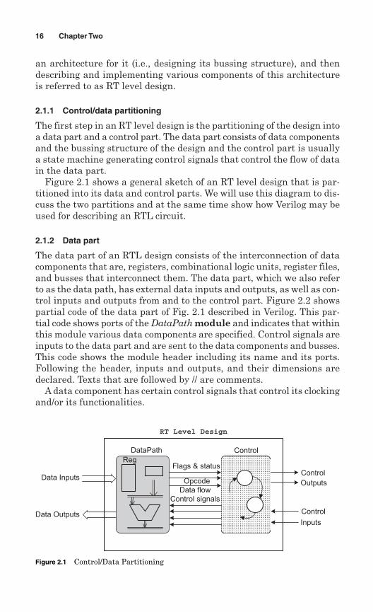
an architecture for it (i.e., designing its bussing structure), and thendescribing and implementing various components of this architectureis referred to as RT level design.
2.1.1 Control/data partitioning
The first step in an RT level design is the partitioning of the design intoa data part and a control part. The data part consists of data componentsand the bussing structure of the design and the control part is usuallya state machine generating control signals that control the flow of datain the data part.
Figure 2.1 shows a general sketch of an RT level design that is par-titioned into its data and control parts. We will use this diagram to dis-cuss the two partitions and at the same time show how Verilog may beused for describing an RTL circuit.
2.1.2 Data part
The data part of an RTL design consists of the interconnection of datacomponents that are, registers, combinational logic units, register files,and busses that interconnect them. The data part, which we also referto as the data path, has external data inputs and outputs, as well as con-trol inputs and outputs from and to the control part. Figure 2.2 showspartial code of the data part of Fig. 2.1 described in Verilog. This par-tial code shows ports of the DataPath module and indicates that withinthis module various data components are specified. Control signals areinputs to the data part and are sent to the data components and busses.This code shows the module header including its name and its ports.Following the header, inputs and outputs, and their dimensions aredeclared. Texts that are followed by // are comments.
A data component has certain control signals that control its clockingand/or its functionalities.
16 Chapter Two
RT Level Design
Flags & status
OpcodeData flow
Control signals
ControlDataPath
Reg
Data Inputs
Data Outputs
Control
Outputs
Control
Inputs
Figure 2.1 Control/Data Partitioning
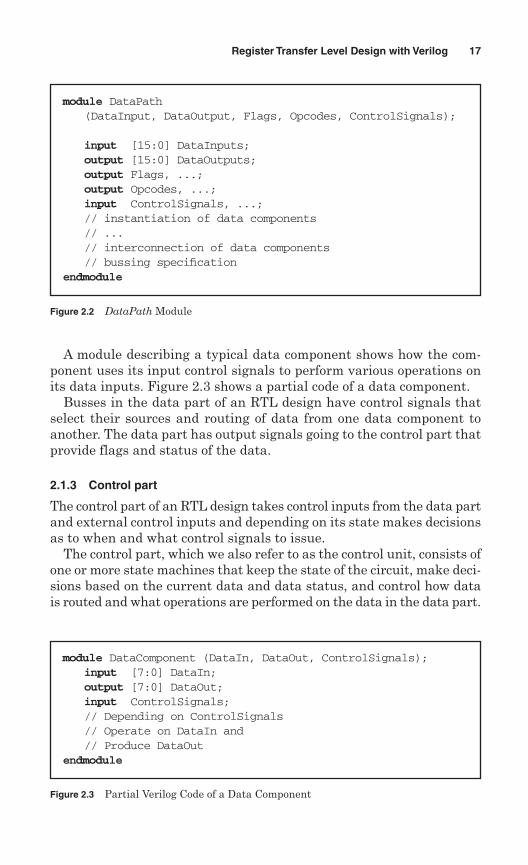
A module describing a typical data component shows how the com-ponent uses its input control signals to perform various operations onits data inputs. Figure 2.3 shows a partial code of a data component.
Busses in the data part of an RTL design have control signals thatselect their sources and routing of data from one data component toanother. The data part has output signals going to the control part thatprovide flags and status of the data.
2.1.3 Control part
The control part of an RTL design takes control inputs from the data partand external control inputs and depending on its state makes decisionsas to when and what control signals to issue.
The control part, which we also refer to as the control unit, consists ofone or more state machines that keep the state of the circuit, make deci-sions based on the current data and data status, and control how datais routed and what operations are performed on the data in the data part.
Register Transfer Level Design with Verilog 17
module DataPath(DataInput, DataOutput, Flags, Opcodes, ControlSignals);
input [15:0] DataInputs;output [15:0] DataOutputs;output Flags, ...;output Opcodes, ...;input ControlSignals, ...;// instantiation of data components // ...// interconnection of data components// bussing specification
endmodule
Figure 2.2 DataPath Module
module DataComponent (DataIn, DataOut, ControlSignals);input [7:0] DataIn;output [7:0] DataOut;input ControlSignals;// Depending on ControlSignals // Operate on DataIn and// Produce DataOut
endmodule
Figure 2.3 Partial Verilog Code of a Data Component
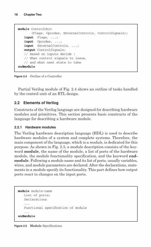
Partial Verilog module of Fig. 2.4 shows an outline of tasks handledby the control unit of an RTL design.
2.2 Elements of Verilog
Constructs of the Verilog language are designed for describing hardwaremodules and primitives. This section presents basic constructs of thelanguage for describing a hardware module.
2.2.1 Hardware modules
The Verilog hardware description language (HDL) is used to describehardware modules of a system and complete systems. Therefore, themain component of the language, which is a module, is dedicated for thispurpose. As shown in Fig. 2.5, a module description consists of the key-word module, the name of the module, a list of ports of the hardwaremodule, the module functionality specification, and the keyword end-module. Following a module name and its list of ports, usually variables,wires, and module parameters are declared. After the declarations, state-ments in a module specify its functionality. This part defines how outputports react to changes on the input ports.
18 Chapter Two
module ControlUnit(Flags, Opcodes, ExternalControls, ControlSignals);
input Flags, ...;input Opcodes, ...;input ExternalControls, ...;output ControlSignals;// Based on inputs decide :// What control signals to issue,// and what next state to take
endmodule
module module-nameList of ports;Declarations...Functional specification of module...
endmodule
Figure 2.4 Outline of a Controller
Figure 2.5 Module Specifications
As in software languages, there is usually more than one way a modulecan be described in Verilog. Various descriptions of a component may cor-respond to descriptions at various levels of abstraction or to various levelsof detail of the functionality of a module. One module description may beat the behavioral level of abstraction with no timing details, while anotherdescription for the same component may include transistor-level timingdetails. Amodule may be part of a library of predesigned library componentsand include detailed timing and loading information, while a differentdescription of the same module may be at the behavioral level for input toa synthesis tool. It must be noted that descriptions of the same module neednot behave in exactly the same way nor is it required that all descriptionsdescribe a behavior correctly. In a fault simulation environment, faultymodules may be developed to study various failure forms of a component.
In the sections that follow we show a small example and several alter-native ways it can be described in Verilog. This presentation is to serveas an introduction to various forms of Verilog constructs for the descrip-tion of hardware.
2.2.2 Primitive instantiations
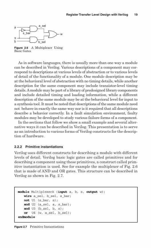
Verilog uses different constructs for describing a module with differentlevels of detail. Verilog basic logic gates are called primitives and fordescribing a component using these primitives, a construct called prim-itive instantiation is used. See for example the multiplexer of Fig. 2.6that is made of AND and OR gates. This structure can be described inVerilog as shown in Fig. 2.7.
Register Transfer Level Design with Verilog 19
a
sb
a_sel
ws_bar
b_sel
Figure 2.6 A Multiplexer UsingBasic Gates
module MultiplexerA (input a, b, s, output w);wire a_sel, b_sel, s_bar;not U1 (s_bar, s);and U2 (a_sel, a, s_bar);and U3 (b_sel, b, s);or U4 (w, a_sel, b_sel);
endmodule
Figure 2.7 Primitive Instantiations
The first line of this code contains the name of the module, MultiplexerA,and its input and output ports. Following this line, intermediate wires aredeclared. The rest of this code consists of instantiation of not, and, and orgates. These instantiations are done according to the diagram of Fig. 2.6,and their wirings are as indicated in this diagram.
2.2.3 Assign statements
Instead of describing a component using primitive gates, boolean expres-sions can be used to describe the logic, and Verilog assign statementscan be used for assigning results of these expressions to various outputs.Our simple multiplexer example can be described as shown in Fig. 2.8.
The statement shown in the body of the MultiplexerB module con-tinuously drives w with its right-hand side expression.
2.2.4 Conditional expression
In cases where the operation of a unit is too complex to be described byboolean expressions, conditional expressions can be used. Our multi-plexer example is described in Fig. 2.9 using an assign statement anda conditional operation.
Because conditional expressions mimic if-then-else behavior of softwarelanguages, they are very effective in describing complex functionalities.Furthermore, the nesting capability of the conditional operator makesit useful in describing a behavior in a very compact way.
2.2.5 Procedural blocks
In cases where the operation of a unit is too complex to be described byassignment of boolean or conditional expressions, higher-level procedural
20 Chapter Two
module MultiplexerB (input a, b, s, output w);assign w = (a & ~s) | (b & s);
endmodule
Figure 2.8 Assign Statement and Boolean
module MultiplexerC (input a, b, s, output w);assign w = s ? b : a;
endmodule
Figure 2.9 Assign Statement and Condition Operator
constructs should be used. Verilog’s main construct for procedural spec-ification of hardware is the always statement used in the example ofFig. 2.10.
The example shown in Fig. 2.10 is still another Verilog code for ourmultiplexer example discussed previously. In this code, an always state-ment, which is the main procedural body of Verilog, encloses an if-elsestatement that assigns a or b to w depending on the value of s.
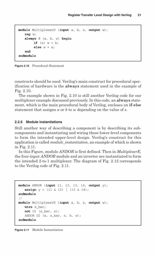
2.2.6 Module instantiations
Still another way of describing a component is by describing its sub-components and instantiating and wiring these lower-level componentsto form the intended upper-level design. Verilog’s construct for thisapplication is called module_instantiation, an example of which is shownin Fig. 2.11.
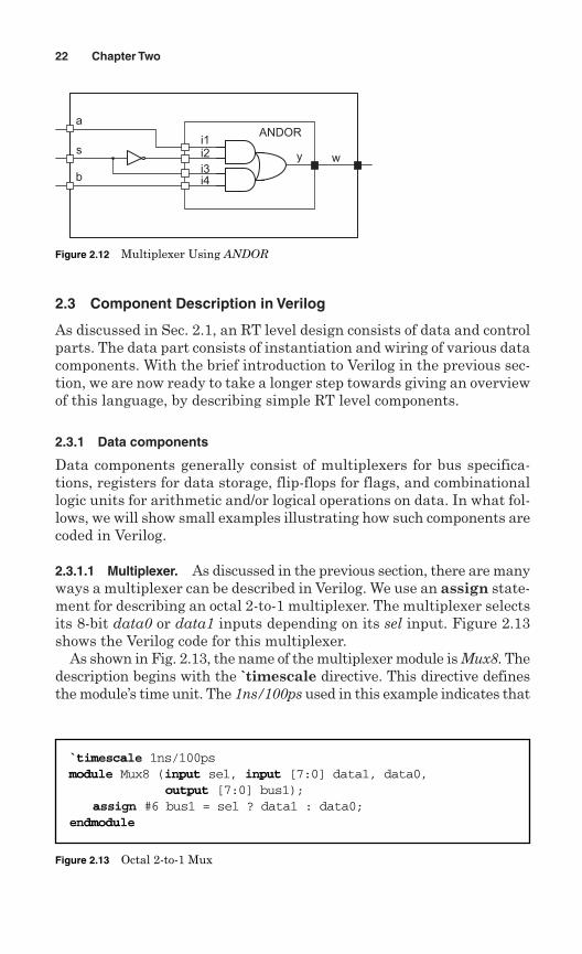
In this Figure, module ANDOR is first defined. Then in MultiplexerE,the four-input ANDOR module and an inverter are instantiated to formthe intended 2-to-1 multiplexer. The diagram of Fig. 2.12 correspondsto the Verilog code of Fig. 2.11.
Register Transfer Level Design with Verilog 21
module MultiplexerD (input a, b, s, output w);reg w;always @ (a, b, s) begin
if (s) w = b;else w = a;
endendmodule
Figure 2.10 Procedural Statement
module ANDOR (input i1, i2, i3, i4, output y);assign y = (i1 & i2) | (i3 & i4);
endmodule//module MultiplexerE (input a, b, s, output w);
wire s_bar;not U1 (s_bar, s);ANDOR U2 (a, s_bar, s, b, w);
endmodule
Figure 2.11 Module Instantiation
2.3 Component Description in Verilog
As discussed in Sec. 2.1, an RT level design consists of data and controlparts. The data part consists of instantiation and wiring of various datacomponents. With the brief introduction to Verilog in the previous sec-tion, we are now ready to take a longer step towards giving an overviewof this language, by describing simple RT level components.
2.3.1 Data components
Data components generally consist of multiplexers for bus specifica-tions, registers for data storage, flip-flops for flags, and combinationallogic units for arithmetic and/or logical operations on data. In what fol-lows, we will show small examples illustrating how such components arecoded in Verilog.
2.3.1.1 Multiplexer. As discussed in the previous section, there are manyways a multiplexer can be described in Verilog. We use an assign state-ment for describing an octal 2-to-1 multiplexer. The multiplexer selectsits 8-bit data0 or data1 inputs depending on its sel input. Figure 2.13shows the Verilog code for this multiplexer.
As shown in Fig. 2.13, the name of the multiplexer module is Mux8. Thedescription begins with the `timescale directive. This directive definesthe module’s time unit. The 1ns/100ps used in this example indicates that
22 Chapter Two
i1i2
i3i4
y w
a
s
b
ANDOR
Figure 2.12 Multiplexer Using ANDOR
`timescale 1ns/100psmodule Mux8 (input sel, input [7:0] data1, data0,
output [7:0] bus1);assign #6 bus1 = sel ? data1 : data0;
endmodule
Figure 2.13 Octal 2-to-1 Mux
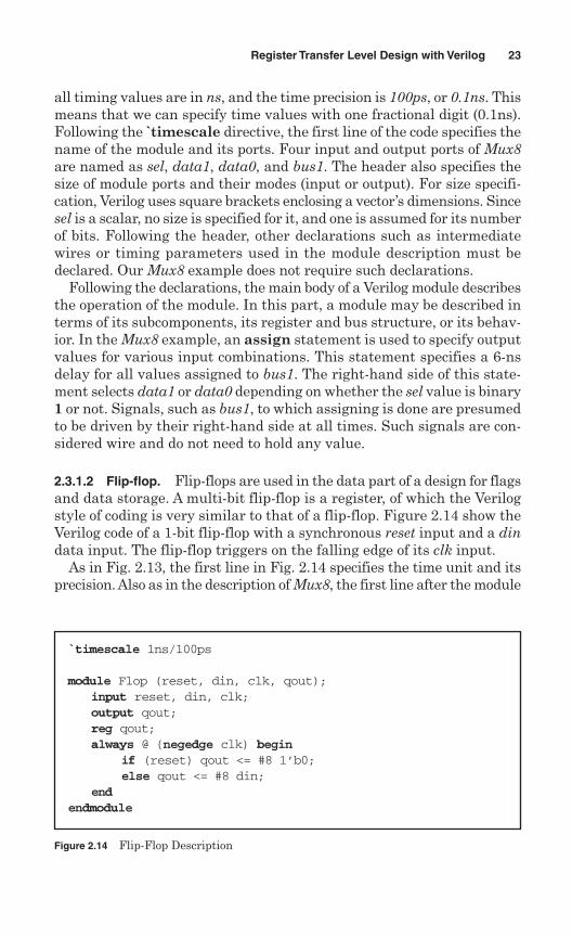
all timing values are in ns, and the time precision is 100ps, or 0.1ns. Thismeans that we can specify time values with one fractional digit (0.1ns).Following the ̀ timescale directive, the first line of the code specifies thename of the module and its ports. Four input and output ports of Mux8are named as sel, data1, data0, and bus1. The header also specifies thesize of module ports and their modes (input or output). For size specifi-cation, Verilog uses square brackets enclosing a vector’s dimensions. Sincesel is a scalar, no size is specified for it, and one is assumed for its numberof bits. Following the header, other declarations such as intermediatewires or timing parameters used in the module description must bedeclared. Our Mux8 example does not require such declarations.
Following the declarations, the main body of a Verilog module describesthe operation of the module. In this part, a module may be described interms of its subcomponents, its register and bus structure, or its behav-ior. In the Mux8 example, an assign statement is used to specify outputvalues for various input combinations. This statement specifies a 6-nsdelay for all values assigned to bus1. The right-hand side of this state-ment selects data1 or data0 depending on whether the sel value is binary1 or not. Signals, such as bus1, to which assigning is done are presumedto be driven by their right-hand side at all times. Such signals are con-sidered wire and do not need to hold any value.
2.3.1.2 Flip-flop. Flip-flops are used in the data part of a design for flagsand data storage. A multi-bit flip-flop is a register, of which the Verilogstyle of coding is very similar to that of a flip-flop. Figure 2.14 show theVerilog code of a 1-bit flip-flop with a synchronous reset input and a dindata input. The flip-flop triggers on the falling edge of its clk input.
As in Fig. 2.13, the first line in Fig. 2.14 specifies the time unit and itsprecision. Also as in the description of Mux8, the first line after the module
Register Transfer Level Design with Verilog 23
`timescale 1ns/100ps
module Flop (reset, din, clk, qout);input reset, din, clk;output qout;reg qout;always @ (negedge clk) begin
if (reset) qout <= #8 1’b0;else qout <= #8 din;
endendmodule
Figure 2.14 Flip-Flop Description
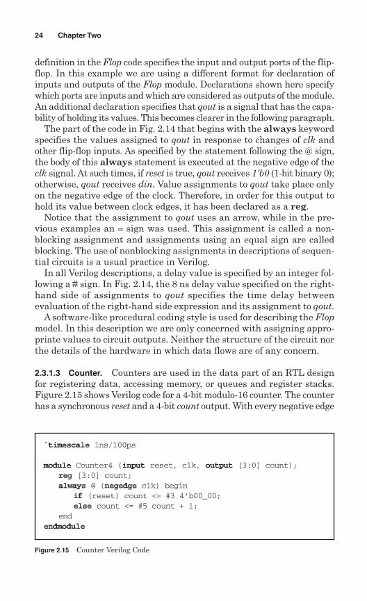
definition in the Flop code specifies the input and output ports of the flip-flop. In this example we are using a different format for declaration ofinputs and outputs of the Flop module. Declarations shown here specifywhich ports are inputs and which are considered as outputs of the module.An additional declaration specifies that qout is a signal that has the capa-bility of holding its values. This becomes clearer in the following paragraph.
The part of the code in Fig. 2.14 that begins with the always keywordspecifies the values assigned to qout in response to changes of clk andother flip-flop inputs. As specified by the statement following the @ sign,the body of this always statement is executed at the negative edge of theclk signal. At such times, if reset is true, qout receives 1'b0 (1-bit binary 0);otherwise, qout receives din. Value assignments to qout take place onlyon the negative edge of the clock. Therefore, in order for this output tohold its value between clock edges, it has been declared as a reg.
Notice that the assignment to qout uses an arrow, while in the pre-vious examples an = sign was used. This assignment is called a non-blocking assignment and assignments using an equal sign are calledblocking. The use of nonblocking assignments in descriptions of sequen-tial circuits is a usual practice in Verilog.
In all Verilog descriptions, a delay value is specified by an integer fol-lowing a # sign. In Fig. 2.14, the 8 ns delay value specified on the right-hand side of assignments to qout specifies the time delay betweenevaluation of the right-hand side expression and its assignment to qout.
A software-like procedural coding style is used for describing the Flopmodel. In this description we are only concerned with assigning appro-priate values to circuit outputs. Neither the structure of the circuit northe details of the hardware in which data flows are of any concern.
2.3.1.3 Counter. Counters are used in the data part of an RTL designfor registering data, accessing memory, or queues and register stacks.Figure 2.15 shows Verilog code for a 4-bit modulo-16 counter. The counterhas a synchronous reset and a 4-bit count output. With every negative edge
24 Chapter Two
`timescale 1ns/100ps
module Counter4 (input reset, clk, output [3:0] count);reg [3:0] count;always @ (negedge clk) begin
if (reset) count <= #3 4’b00_00;else count <= #5 count + 1;
endendmodule
Figure 2.15 Counter Verilog Code
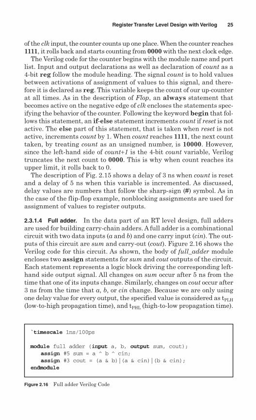
of the clk input, the counter counts up one place. When the counter reaches1111, it rolls back and starts counting from 0000 with the next clock edge.
The Verilog code for the counter begins with the module name and portlist. Input and output declarations as well as declaration of count as a4-bit reg follow the module heading. The signal count is to hold valuesbetween activations of assignment of values to this signal, and there-fore it is declared as reg. This variable keeps the count of our up-counterat all times. As in the description of Flop, an always statement thatbecomes active on the negative edge of clk encloses the statements spec-ifying the behavior of the counter. Following the keyword begin that fol-lows this statement, an if-else statement increments count if reset is notactive. The else part of this statement, that is taken when reset is notactive, increments count by 1. When count reaches 1111, the next counttaken, by treating count as an unsigned number, is 10000. However,since the left-hand side of count+1 is the 4-bit count variable, Verilogtruncates the next count to 0000. This is why when count reaches itsupper limit, it rolls back to 0.
The description of Fig. 2.15 shows a delay of 3 ns when count is resetand a delay of 5 ns when this variable is incremented. As discussed,delay values are numbers that follow the sharp-sign (#) symbol. As inthe case of the flip-flop example, nonblocking assignments are used forassignment of values to register outputs.
2.3.1.4 Full adder. In the data part of an RT level design, full addersare used for building carry-chain adders. A full adder is a combinationalcircuit with two data inputs (a and b) and one carry input (cin). The out-puts of this circuit are sum and carry-out (cout). Figure 2.16 shows theVerilog code for this circuit. As shown, the body of full_adder moduleencloses two assign statements for sum and cout outputs of the circuit.Each statement represents a logic block driving the corresponding left-hand side output signal. All changes on sum occur after 5 ns from thetime that one of its inputs change. Similarly, changes on cout occur after3 ns from the time that a, b, or cin change. Because we are only usingone delay value for every output, the specified value is considered as tPLH
(low-to-high propagation time), and tPHL (high-to-low propagation time).
Register Transfer Level Design with Verilog 25
`timescale 1ns/100ps
module full adder (input a, b, output sum, cout);assign #5 sum = a ^ b ^ cin;assign #3 cout = (a & b)|(a & cin)|(b & cin);
endmodule
Figure 2.16 Full adder Verilog Code
In our example we are using two assign statements in the statementpart of the full_adder module. This part of a module is considered as aconcurrent body of Verilog. The order of statements in this section is notimportant and all statements are sensitive to their sensitivity list, mean-ing that they execute when an event occurs on any of their right-handside signals. Sensitivity lists are discussed further on.
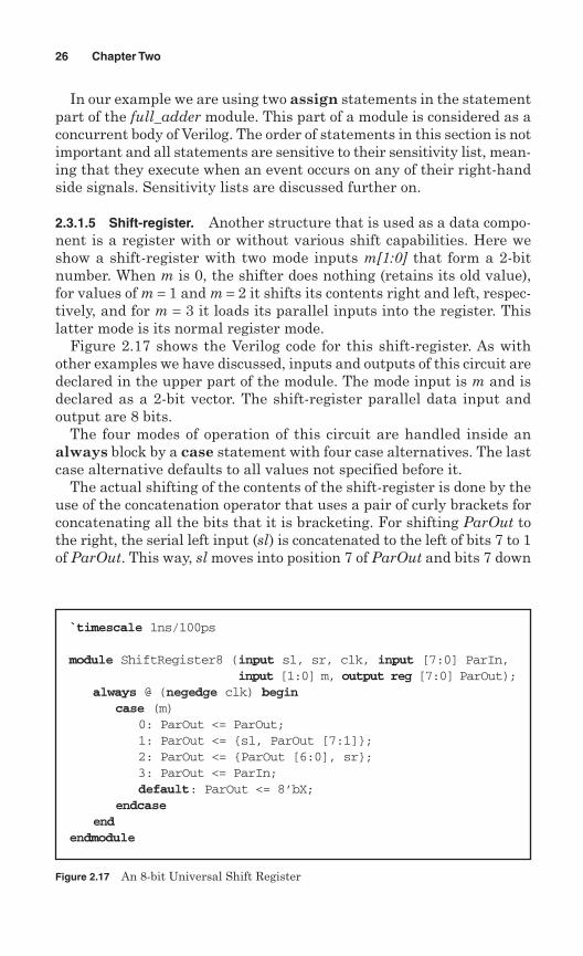
2.3.1.5 Shift-register. Another structure that is used as a data compo-nent is a register with or without various shift capabilities. Here weshow a shift-register with two mode inputs m[1:0] that form a 2-bitnumber. When m is 0, the shifter does nothing (retains its old value),for values of m = 1 and m = 2 it shifts its contents right and left, respec-tively, and for m = 3 it loads its parallel inputs into the register. Thislatter mode is its normal register mode.
Figure 2.17 shows the Verilog code for this shift-register. As withother examples we have discussed, inputs and outputs of this circuit aredeclared in the upper part of the module. The mode input is m and isdeclared as a 2-bit vector. The shift-register parallel data input andoutput are 8 bits.
The four modes of operation of this circuit are handled inside analways block by a case statement with four case alternatives. The lastcase alternative defaults to all values not specified before it.
The actual shifting of the contents of the shift-register is done by theuse of the concatenation operator that uses a pair of curly brackets forconcatenating all the bits that it is bracketing. For shifting ParOut tothe right, the serial left input (sl) is concatenated to the left of bits 7 to 1of ParOut. This way, sl moves into position 7 of ParOut and bits 7 down
26 Chapter Two
`timescale 1ns/100ps
module ShiftRegister8 (input sl, sr, clk, input [7:0] ParIn,input [1:0] m, output reg [7:0] ParOut);
always @ (negedge clk) begincase (m)
0: ParOut <= ParOut;1: ParOut <= {sl, ParOut [7:1]};2: ParOut <= {ParOut [6:0], sr};3: ParOut <= ParIn;default: ParOut <= 8’bX;
endcaseend
endmodule
Figure 2.17 An 8-bit Universal Shift Register
to 1 move into positions 6 down to 0 of this register. Similarly, for shift-ing ParOut to the left, the serial right (sr) input is concatenated to theright of bits 6 down to 0 of this register. This causes sr to be clocked inbit 0 of ParOut, and ParOut[6:0] to be clocked into ParOut[7:1], caus-ing a left shift of this register.
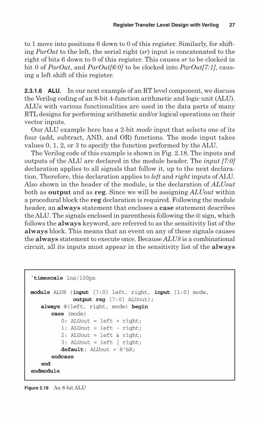
2.3.1.6 ALU. In our next example of an RT level component, we discussthe Verilog coding of an 8-bit 4-function arithmetic and logic unit (ALU).ALUs with various functionalities are used in the data parts of manyRTL designs for performing arithmetic and/or logical operations on theirvector inputs.
Our ALU example here has a 2-bit mode input that selects one of itsfour (add, subtract, AND, and OR) functions. The mode input takesvalues 0, 1, 2, or 3 to specify the function performed by the ALU.
The Verilog code of this example is shown in Fig. 2.18. The inputs andoutputs of the ALU are declared in the module header. The input [7:0]declaration applies to all signals that follow it, up to the next declara-tion. Therefore, this declaration applies to left and right inputs of ALU.Also shown in the header of the module, is the declaration of ALUoutboth as output and as reg. Since we will be assigning ALUout withina procedural block the reg declaration is required. Following the moduleheader, an always statement that encloses a case statement describesthe ALU. The signals enclosed in parenthesis following the @ sign, whichfollows the always keyword, are referred to as the sensitivity list of thealways block. This means that an event on any of these signals causesthe always statement to execute once. Because ALU8 is a combinationalcircuit, all its inputs must appear in the sensitivity list of the always
Register Transfer Level Design with Verilog 27
`timescale 1ns/100ps
module ALU8 (input [7:0] left, right, input [1:0] mode,output reg [7:0] ALUout);
always @(left, right, mode) begincase (mode)
0: ALUout = left + right;1: ALUout = left - right;2: ALUout = left & right;3: ALUout = left | right;default: ALUout = 8’bX;
endcaseend
endmodule
Figure 2.18 An 8-bit ALU
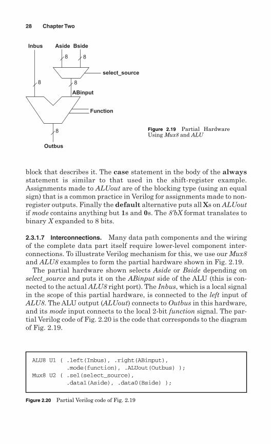
block that describes it. The case statement in the body of the alwaysstatement is similar to that used in the shift-register example.Assignments made to ALUout are of the blocking type (using an equalsign) that is a common practice in Verilog for assignments made to non-register outputs. Finally the default alternative puts all Xs on ALUoutif mode contains anything but 1s and 0s. The 8’bX format translates tobinary X expanded to 8 bits.
2.3.1.7 Interconnections. Many data path components and the wiringof the complete data part itself require lower-level component inter-connections. To illustrate Verilog mechanism for this, we use our Mux8and ALU8 examples to form the partial hardware shown in Fig. 2.19.
The partial hardware shown selects Aside or Bside depending onselect_source and puts it on the ABinput side of the ALU (this is con-nected to the actual ALU8 right port). The Inbus, which is a local signalin the scope of this partial hardware, is connected to the left input ofALU8. The ALU output (ALUout) connects to Outbus in this hardware,and its mode input connects to the local 2-bit function signal. The par-tial Verilog code of Fig. 2.20 is the code that corresponds to the diagramof Fig. 2.19.
28 Chapter Two
BsideAsideInbus
select_source
ABinput
Function
Outbus
8
8 8
8
8
Figure 2.19 Partial HardwareUsing Mux8 and ALU
ALU8 U1 ( .left(Inbus), .right(ABinput),.mode(function), .ALUout(Outbus) );
Mux8 U2 ( .sel(select_source), .data1(Aside), .data0(Bside) );
Figure 2.20 Partial Verilog code of Fig. 2.19
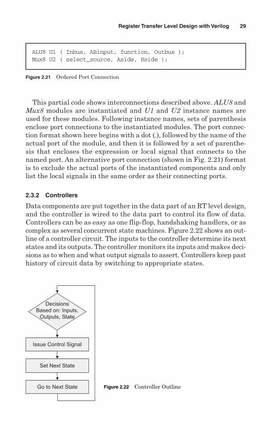
This partial code shows interconnections described above. ALU8 andMux8 modules are instantiated and U1 and U2 instance names areused for these modules. Following instance names, sets of parenthesisenclose port connections to the instantiated modules. The port connec-tion format shown here begins with a dot (.), followed by the name of theactual port of the module, and then it is followed by a set of parenthe-sis that encloses the expression or local signal that connects to thenamed port. An alternative port connection (shown in Fig. 2.21) formatis to exclude the actual ports of the instantiated components and onlylist the local signals in the same order as their connecting ports.
2.3.2 Controllers
Data components are put together in the data part of an RT level design,and the controller is wired to the data part to control its flow of data.Controllers can be as easy as one flip-flop, handshaking handlers, or ascomplex as several concurrent state machines. Figure 2.22 shows an out-line of a controller circuit. The inputs to the controller determine its nextstates and its outputs. The controller monitors its inputs and makes deci-sions as to when and what output signals to assert. Controllers keep pasthistory of circuit data by switching to appropriate states.
Register Transfer Level Design with Verilog 29
ALU8 U1 ( Inbus, ABinput, function, Outbus );Mux8 U2 ( select_source, Aside, Bside );
Figure 2.21 Ordered Port Connection
Issue Control Signal
Go to Next State
DecisionsBased on: Inputs,
Outputs, State
Set Next State
Figure 2.22 Controller Outline
This section presents two examples to illustrate some of the featuresof Verilog for describing state machines.
2.3.2.1 Synchronizer. When inputs to a clocked circuit are generated bya system that is run by a different clock, or by an external asynchronouscircuit, a synchronizer is used to synchronize incoming data with agiven clock. Figure 2.23 shows an asynchronous data signal (adata) andan output that is synchronized with the positive-edge of the clk signal.
Figure 2.24 shows the Verilog module for generating the synched signalof Fig. 2.23. The module header declares inputs and outputs of this circuit,and within this module an always block handles the synchronization. Asshown, the flow into the always block begins when the positive edge ofclk is detected. At this time if adata is 0, the output synched signal remains0 for the next clock period. If a 1 is detected on adata on the rising edgeof the clock, synched becomes 1 and remains 1 for at least one clock period,at which time it may be set to 0 if adata is 0. Since the flow into thealways block only begins on the rising edge of the clk, it is guaranteed thatchanges of synched only occur with this clock edge. The description shownassumes that only 0 and 1 values can appear on the adata input.
2.3.2.2 Sequence detector. While being simple in description and func-tionality, a sequence detector is a good representation for the generalclass of controllers. In other words, sequence detectors are simplified con-trollers. Instead of many inputs and outputs, sequence detectors have oneor two input and output lines, and instead of complex decision makings
30 Chapter Two
Clk
adata
synched
Figure 2.23 Synchronizing adata
`timescale 1ns/100ps
module Synchronizer (input clk, adata, output reg synched);always @ (posedge clk)
if (adata == 0) synched <= 0; else synched <= 1;endmodule
Figure 2.24 A Simple Synchronization Circuit
and input conditions, sequence detectors generally search for a sequenceof 1s and 0s on their input. We will present a Verilog description for thesimple sequence detector shown in Fig. 2.25.
A Moore machine sequence detector, the pseudo-code of which is shownin Fig. 2.27, searches on it’s a input for the 110 sequence. When thissequence is detected in three consecutive clock pulses, the output (w)becomes 1 and stays 1 for a complete clock cycle. The state machine forthis detector is shown in Fig. 2.26. States of the machine are named s0,s1, s2, and s3. The s0 state is the reset state and s3 is the state in whichthe 110 sequence is detected. The reset input of this machine resets itto its s0 state. Starting in this state, it takes at least three clock peri-ods for the machine to get to the s3 state, in which output becomes 1.
The Verilog behavioral description of this machine is shown in Fig. 2.27.The list of ports are a, clk, reset, and w. A parameter declaration in thisdescription defines constants s0, s1, s2, and s3 to be used for the names ofthe states of this machine. Assigning binary values assigned to theseparameters, can be regarded as making state assignments.
The two-bit reg declaration declares current as the variable thatholds the current state of the machine. This variable corresponds to a2-bit register, which represents the state variables of this machine.
The main flow of the state machine is implemented by an alwaysblock that is sensitive to the positive edge of the clock. In this statementan if-else statement checks for reset, and in case of the absence of a 1on this inputs, state transitions are taken care of by a case statement.
Register Transfer Level Design with Verilog 31
clk
aIf 110 is detectedon a, then w gets1, else w gets 0.
W
Figure 2.25 State Machine Description
01
1
1
0
0
1
0reset
S00 0
S1
0
S2
0
S3
Figure 2.26 Sequence Detector State Machine
The four case alternatives of the case statement each correspond to astate of the state machine. Figure 2.28 shows state s2, its next state, andthe corresponding Verilog code in the always block of Fig. 2.27.
The body of the Detector110 module has an assign statement thatassigns a 1 to the w output when the machine reaches the s3 state. Thisstatement is outside of the always block and represents a combinational
32 Chapter Two
`timescale 1ns/100ps
module Detector110 (input a, clk, reset, output w);parameter [1:0] s0=2’b00, s1=2’b01, s2=2’b10, s3=2’b11;reg [1:0] current;
always @ (posedge clk) beginif (reset) current = s0;else
case (current)s0: if (a) current <= s1; else current <= s0;s1: if (a) current <= s2; else current <= s0;s2: if (a) current <= s2; else current <= s3;s3: if (a) current <= s1; else current <= s0;endcase
end
assign w = (current == s3) ? 1: 0;
endmodule
Figure 2.27 Verilog Code for 110 Detector
a=0
s0
0
s2
0
s1
0
a=1
s1:
if (a)
current <= s2;
else
current <= s0;
Figure 2.28 State Transitions and CorrespondingVerilog Code
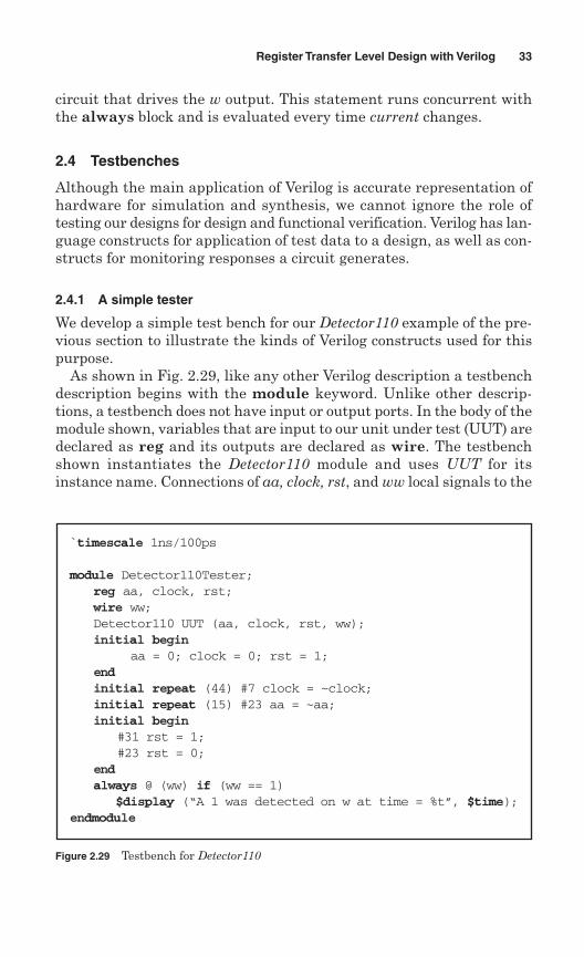
circuit that drives the w output. This statement runs concurrent withthe always block and is evaluated every time current changes.
2.4 Testbenches
Although the main application of Verilog is accurate representation ofhardware for simulation and synthesis, we cannot ignore the role oftesting our designs for design and functional verification. Verilog has lan-guage constructs for application of test data to a design, as well as con-structs for monitoring responses a circuit generates.
2.4.1 A simple tester
We develop a simple test bench for our Detector110 example of the pre-vious section to illustrate the kinds of Verilog constructs used for thispurpose.
As shown in Fig. 2.29, like any other Verilog description a testbenchdescription begins with the module keyword. Unlike other descrip-tions, a testbench does not have input or output ports. In the body of themodule shown, variables that are input to our unit under test (UUT) aredeclared as reg and its outputs are declared as wire. The testbenchshown instantiates the Detector110 module and uses UUT for itsinstance name. Connections of aa, clock, rst, and ww local signals to the
Register Transfer Level Design with Verilog 33
`timescale 1ns/100ps
module Detector110Tester;reg aa, clock, rst; wire ww;Detector110 UUT (aa, clock, rst, ww);initial begin
aa = 0; clock = 0; rst = 1;endinitial repeat (44) #7 clock = ~clock;initial repeat (15) #23 aa = ~aa;initial begin
#31 rst = 1;#23 rst = 0;
endalways @ (ww) if (ww == 1)
$display (“A 1 was detected on w at time = %t”, $time);endmodule
Figure 2.29 Testbench for Detector110
ports of Detector110 are done according to the order in which these portsappear in the port list of the detector circuit.
We are using initial statements to drive test values into the variablesthat are connected to the inputs of the detector. An initial statementis a procedural statement that runs once and stops when it reaches itslast statement. All initial blocks in a module, start at time 0 and runconcurrently.
In the body of our testbench, an initial statement is used for initializ-ing the input signals. Following this statement, another initial statementrepeats 44 times of complementing the clock input with 7 ns delay values.This generates a periodic signal on clock. Signal aa is also assigned a peri-odic signal, but with a different frequency. The last initial statementshown waits 31 ns before assigning a 1 to rst and another 23 ns beforeassigning a 0 to this variable. This is intended to cover several clockedges in order to reset the machine.
The last statement in the body of the Detector110tester module is analways statement that reports the times at which the ww variablebecomes 1. Recall that this variable is connected to the output of oursequence detector. The always block wakes up when ww changes. If thechange on ww has caused it to become 1, a statement displaying a noteand the time of occurrence of ww will be issued. This note will appearin the simulation environment’s window that is often referred to as the“console” or “transcript”. The $display task is a Verilog system task.
2.4.2 Tasks and functions
The testbench of Fig. 2.29 shows utilization of the $display system task.In addition to system tasks for input, output, display, and timing checks,Verilog allows definition and utilization of user defined tasks and functions.
A task can represent a sub module within a Verilog module. A taskbegins with the task keyword and for its header uses a format that isvery similar to that of a module. The body of a task can only consist ofprocedural statements like if-else and case.
Functions can also be used for corresponding to hardware entities, orthey may be used for writing structured codes, in much the same way asthey are used in software languages. Typical applications of functionsinclude representation of boolean functions, data and code conversion,and input and output data formatting. Generally, any time the final valueof a process is used on the right-hand side of an expression, a function canbe used to simplify the expression.
2.5 Summary
This chapter gave an overview of Verilog and its use for design and testof RT level description. After discussing components of an RT leveldesign, we used small examples to illustrate such components and at the
34 Chapter Two
same time showed Verilog coding of hardware modules. The descriptionspresented in this part were all synthesizable and had a one-to-one hard-ware correspondence. To make the discussion of the language complete,and show alternatives of the use of this language in a design, we showedhow testbenches could be developed in Verilog. In this part several newconstructs of Verilog were presented.
Problems
2.1 Write a behavioral description for a 4-to-1 multiplexer. The multiplexer hass1 and s0 select inputs and four data inputs.
2.2 Using an assign statement describe a majority circuit with three inputsand one output. When the majority of the inputs are 1, the output of the majoritycircuit becomes 1.
2.3 Write a Verilog description for a 101 sequence detector with an a input anda w output.
2.4 Write a testbench for the 101 detector of Prob. 2.3. Make sure you applyan input sequence to make the output become 1.
Suggested Reading
IEEE Std 1364-2001, IEEE Standard Verilog Language Reference Manual, SH94921-TBR (print) SS94921-TBR (electronic), ISBN 0-7381-2827-9 (print and electronic),2001.
Navabi, Z., “Digital Design and Implementation with Field Programmable Devices”,Kluwer Academic Publishers, Boston, MA, 2005, ISBN: 1-4020-8011-5.
Navabi, Z., “Verilog Computer-Based Training Course”; CBT CD with hardcopy User’smanual, McGraw-Hill, New York, 2002 ISBN 0-07-137473-6.
Register Transfer Level Design with Verilog 35

This page intentionally left blank
Chapter
3Verilog Language Concepts
Because Verilog is a language for description of hardware, it has featuresthat are conceptually different from those of software languages. Twomain features that characterize hardware languages are timing and con-currency. Timing is associated with values that are assigned to hardwarecarriers, while concurrency refers to simultaneous operation of varioushardware components. Because of these features, data types and opera-tors take new definitions in hardware languages and must be looked atdifferently from those of software languages. This chapter defines timingand concurrency and then it discusses Verilog language constructs thatmake it an efficient language for design and test of hardware modules.
3.1 Characterizing Hardware Languages
Timing and concurrency are the main characteristics of hardwaredescription languages. These features are instrumental in the correctdescription of hardware components at various levels of abstraction.
3.1.1 Timing
Transfer of values between hardware components or within a componentis done through wires or busses. Variables in Verilog may be used forrepresentation of actual wires, and because of delays associated with thetransfer of values through wires, variable assignments in Verilog caninclude timing specification. Consider, for example, the AND-OR circuitof Fig. 3.1. This circuit can be simply described by a boolean equationas shown below. (Note that, & is AND, | is OR, and ~ is NOT).
assign w1 = a & b | a & ~b;
37
Copyright © 2006 by The McGraw-Hill Publishing Companies, Inc. Click here for terms of use.
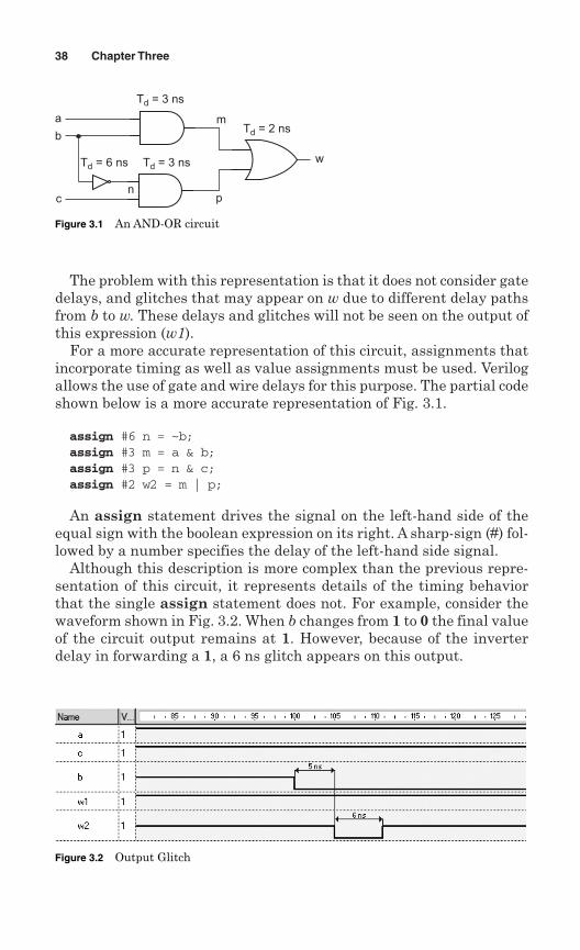
The problem with this representation is that it does not consider gatedelays, and glitches that may appear on w due to different delay pathsfrom b to w. These delays and glitches will not be seen on the output ofthis expression (w1).
For a more accurate representation of this circuit, assignments thatincorporate timing as well as value assignments must be used. Verilogallows the use of gate and wire delays for this purpose. The partial codeshown below is a more accurate representation of Fig. 3.1.
assign #6 n = ~b;assign #3 m = a & b;assign #3 p = n & c;assign #2 w2 = m | p;
An assign statement drives the signal on the left-hand side of theequal sign with the boolean expression on its right. A sharp-sign (#) fol-lowed by a number specifies the delay of the left-hand side signal.
Although this description is more complex than the previous repre-sentation of this circuit, it represents details of the timing behaviorthat the single assign statement does not. For example, consider thewaveform shown in Fig. 3.2. When b changes from 1 to 0 the final valueof the circuit output remains at 1. However, because of the inverterdelay in forwarding a 1, a 6 ns glitch appears on this output.
38 Chapter Three
w
a
b
c p
m
Td = 3 ns
Td = 2 ns
Td = 6 ns
n
Td = 3 ns
Figure 3.1 An AND-OR circuit
Figure 3.2 Output Glitch
As shown in this figure, w1, which is the result of the single assignstatement, does not show the delay, while w2 shows both propagationdelays and glitches that may occur on the w output of circuit of Fig. 3.1.
From the above discussion, we conclude that accurate representationof hardware requires handling of timing, and a language for modelinghardware must have constructs for doing so. The Verilog HDL allowsmany schemes for incorporating timing into description of hardware.Constructs of this language are tailored to have such timing specifications.
3.1.2 Concurrency
Like timing, concurrency is an essential feature of any language for descrip-tion of hardware. When a software programmer develops code for per-forming a certain task, he or she thinks of this task in a sequential manner.The software developed this way will have a top down sequential flow. Onthe other hand, when a hardware designer or modeler is to describe a hard-ware system, he or she thinks of this hardware as interconnections of com-ponents. The functionality of the overall system is achieved by concurrentlyactive components communicating through their input and output ports.The functionality of each component may be described by concurrent sub-components or described by a program in a sequential manner.
We refer to concurrency as the way the simulation of components orconstructs appears to the user. Obviously, Verilog is a language forwhich simulators have been developed on single-processor platforms,and true concurrency in the execution of thousands of componentscannot exist. Through the use of concurrent constructs, timing of inter-connecting signals, and order of simulation of constructs or components,a Verilog simulator makes us (the users) think that such execution isbeing done concurrently.
Going back to our example of the AND-OR circuit, the gates of the cir-cuit of Fig. 3.1 are concurrently active. This means that we cannotdecide on a pre-determined order in which these gates perform theiroperations. Instead, while hand simulating this circuit, we evaluate agate only when its input changes. Similarly, the four assign statementsthat we discussed for representing this circuit are regarded as concur-rent. The order in which these statements appear in a concurrent bodyof Verilog is not important. As in its corresponding hardware, each state-ment only evaluates its boolean expression when an event occurs on oneof its right-hand side signals.
For example, if the assign statement driving w2 appears first in thelist of statements shown, the result will be no different than if it appearslast, as it is now. In Verilog, the body of a module is referred to as a con-current body, and encloses statements that are concurrently active.
Although individual hardware components of a system are concur-rent, for describing behavior of a component, it is sometimes easier for
Verilog Language Concepts 39
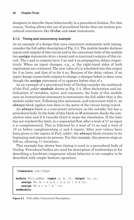
designers to describe them behaviorally in a procedural fashion. For thisreason, Verilog allows the use of procedural blocks that can enclose pro-cedural statements like if-else and case statements.
3.1.3 Timing and concurrency example
As an example of a design that uses concurrent statements with timing,consider the full-adder description of Fig. 3.3. The module header declaresinputs and outputs of this circuit and in the concurrent body of the moduletwo assign statements drive s (sum) and co (carryout) outputs of this cir-cuit. The s and co outputs have 3 ns and 4 ns propagation delays respec-tively. When an input changes, e.g., a, the right-hand sides of bothexpressions are evaluated. The new value of s is scheduled into this outputfor 3 ns later, and that of co for 4 ns. Because of the delay values, if aninput change causes both outputs to change, s changes before co does, eventhough the assign statement of co appears before that of s.
As an example of a procedural body of Verilog consider the testbenchof the Full_adder module shown in Fig. 3.4. After declaration and ini-tialization of variables, wires, and constants, the body of this moduleuses an instantiation statement to instantiate the full adder that is themodule under test. Following this statement, and concurrent with it, analways block applies test data to the ports of the circuit being tested.
An always block is a concurrent structure on the outside, but has aprocedural body. In the body of this block an if-statement checks the sim-ulation time and if it exceeds tlimit it stops the simulation. If the timehas not reached this limit, in a sequential flow, after a wait of 17 ns inputa is complemented. This is followed by a wait of 13 ns and a wait of19 ns before complementing ci and b inputs. After new values havebeen given to the inputs of Full_adder, the always block returns to itsbeginning and repeats its process. For this example, this process stops at539 ns, allowing 11 iterations.
This example has shown how timing is used in a procedural body ofVerilog. Procedural bodies are used for description of testbenches or fordescribing a hardware component whose behavior is too complex to bedescribed with simple boolean equations.
40 Chapter Three
`timescale 1ns/100ps
module Full_adder (input a, b, ci, output co, s);assign #4 co = a & b | a & ci | b & ci;assign #3 s = a ^ b ^ ci;
endmodule
Figure 3.3 Full adder Concurrent Description
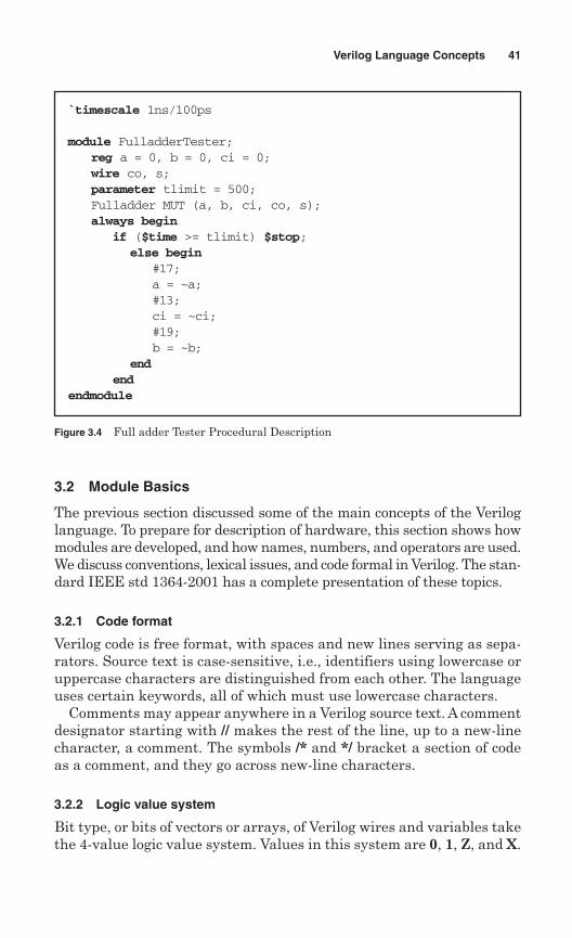
3.2 Module Basics
The previous section discussed some of the main concepts of the Veriloglanguage. To prepare for description of hardware, this section shows howmodules are developed, and how names, numbers, and operators are used.We discuss conventions, lexical issues, and code formal in Verilog. The stan-dard IEEE std 1364-2001 has a complete presentation of these topics.
3.2.1 Code format
Verilog code is free format, with spaces and new lines serving as sepa-rators. Source text is case-sensitive, i.e., identifiers using lowercase oruppercase characters are distinguished from each other. The languageuses certain keywords, all of which must use lowercase characters.
Comments may appear anywhere in a Verilog source text. A commentdesignator starting with // makes the rest of the line, up to a new-linecharacter, a comment. The symbols /* and */ bracket a section of codeas a comment, and they go across new-line characters.
3.2.2 Logic value system
Bit type, or bits of vectors or arrays, of Verilog wires and variables takethe 4-value logic value system. Values in this system are 0, 1, Z, and X.
Verilog Language Concepts 41
`timescale 1ns/100ps
module FulladderTester;reg a = 0, b = 0, ci = 0; wire co, s; parameter tlimit = 500;Fulladder MUT (a, b, ci, co, s);always begin
if ($time >= tlimit) $stop;else begin
#17;a = ~a;#13;ci = ~ci;#19;b = ~b;
endend
endmodule
Figure 3.4 Full adder Tester Procedural Description
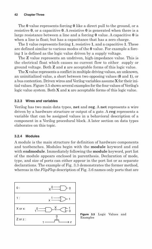
The 0 value represents forcing 0 like a direct pull to the ground, or aresistive 0, or a capacitive 0. A resistive 0 is generated when there is alarge resistance between a line and a forcing 0 value. A capacitive 0 iswhen a line is float; but has a capacitance that has a zero charge.
The 1 value represents forcing 1, resistive 1, and a capacitive 1. Theseare defined similar to various modes of the 0 value. For example a forc-ing 1 is defined as the logic value driven by a supply voltage.
The Z value represents an undriven, high-impedance value. This isthe electrical float which causes no current flow to either supply orground voltage. Both Z and z are acceptable forms of this logic value.
The X value represents a conflict in multiple driving values, an unknown,an uninitialized value, a short between two opposing values (0 and 1), ora bus contention. Driven wires and Verilog variables assume X for their ini-tial values. Figure 3.5 shows several examples for the four values of Verilog’slogic value system. Both X and x are acceptable forms of this logic value.
3.2.3 Wires and variables
Verilog has two main data types, net and reg. A net represents a wiredriven by a hardware structure or output of a gate. A reg represents avariable that can be assigned values in a behavioral description of acomponent in a Verilog procedural block. A later section on data typeselaborates on this topic.
3.2.4 Modules
A module is the main structure for definition of hardware componentsand testbenches. Modules begin with the module keyword and endwith endmodule. Immediately following the module keyword, port listof the module appears enclosed in parenthesis. Declaration of mode,type, and size of ports can either appear in the port list or as separatedeclarations. The example of Fig. 3.3 demonstrates the former method,whereas in the FlipFlop description of Fig. 3.6 names only ports that are
42 Chapter Three
0X 0
1 0
X01
1x 1
0 :
1 :
Z or z :
X or x:
0
z1
Figure 3.5 Logic Values andExamples
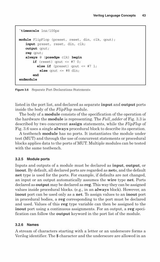
listed in the port list, and declared as separate input and output portsinside the body of the FlipFlop module.
The body of a module consists of the specification of the operation ofthe hardware the module is representing. The Full_adder of Fig. 3.3 isdescribed by two concurrent assign statements, while the FlipFlop ofFig. 3.6 uses a single always procedural block to describe its operation.
A testbench module has no ports. It instantiates the module undertest (MUT) and through the use of concurrent statements or proceduralblocks applies data to the ports of MUT. Multiple modules can be testedwith the same testbench.
3.2.5 Module ports
Inputs and outputs of a module must be declared as input, output, orinout. By default, all declared ports are regarded as nets, and the defaultnet type is used for the ports. For example, if defaults are not changed,an input or an output automatically assumes the wire type net. Portsdeclared as output may be declared as reg. This way they can be assignedvalues inside procedural blocks. (e.g., in an always block). However, aninout port can be used only as a net. To assign values to an inout portin procedural bodies, a reg corresponding to the port must be declaredand used. Values of this reg type variable can then be assigned to theinout port using a continuous assignments. For an output, a reg speci-fication can follow the output keyword in the port list of the module.
3.2.6 Names
A stream of characters starting with a letter or an underscore forms aVerilog identifier. The $ character and the underscore are allowed in an
Verilog Language Concepts 43
`timescale 1ns/100ps
module FlipFlop (preset, reset, din, clk, qout);input preset, reset, din, clk;output qout;reg qout;always @ (posedge clk) begin
if (reset) qout <= #7 0;else if (preset) qout <= #7 1;else qout <= #8 din;
endendmodule
Figure 3.6 Separate Port Declarations Statements
identifier. A stream of special characters may be used as an identifier ifpreceded by a backslash character. Verilog uses keywords that are allformed by streams of lowercase characters. In our examples, we use boldtype for Verilog codes for keywords.
System tasks and functions are part of the Verilog standard. Thenames of these utilities begin with a $ character. An example systemtask is $display, which is used for formatted output. System tasks andfunctions will be discussed later in this chapter.
The Verilog language defines a number of compiler directives that willbe discussed later. Compiler directive names are preceded by the ̀ (backsingle quote) character. An example is the `timescale directive, whichdefines the time unit for a Verilog code in a source text. The followingare valid names for identifiers.
aname , name1 , _name , Name ,Name$ , name55 , _55name , setup ,_$name.
And, the following are Verilog keywords or system tasks.
$display default $setupbegin tri1 small
3.2.7 Numbers
Constants in Verilog are integer or real. Specification of integers caninclude X (or x) and Z (or z) in addition to the standard 0 and 1 logicvalues.
Integer formats provide various ways for representing bit streams.Integers may be sized or unsized. A sized integer begins with the numberof equivalent bits, followed by the single quote character ('), a base speci-fier, and the digits of the number in the specified base. The base specifieris a single lower or uppercase character, b, d, o, or h for binary, decimal,octal, and hexadecimal bases. The general format for integers is:
number_of_bits ‘base_identifier digits
Digits in the decimal (d) system are 0 through 9. For hexadecimal,octal, and binary systems, in addition to their standard digits, X and Z(both upper and lowercase) characters are also allowed. Hexadecimaland octal X and Z digits expand to 4 or 3 bits of X and Z respectively. Anumber without the number_of_bits specification is regarded as anunsized number.
44 Chapter Three
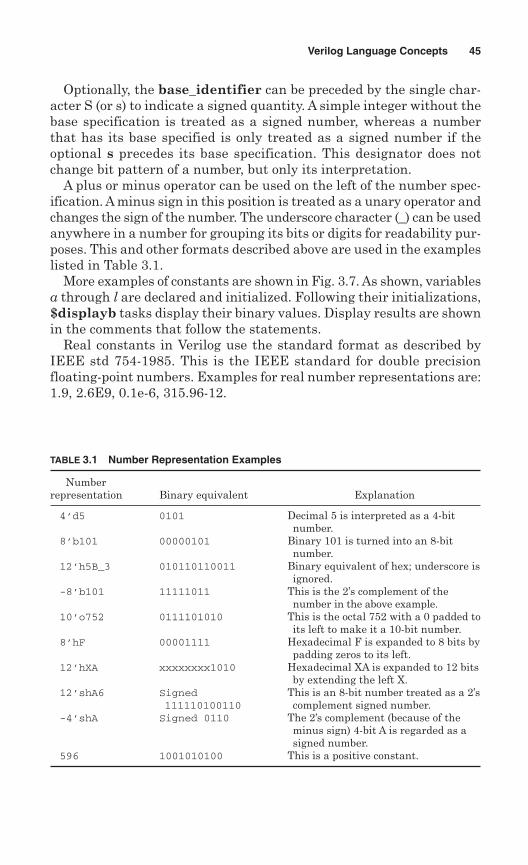
Optionally, the base_identifier can be preceded by the single char-acter S (or s) to indicate a signed quantity. A simple integer without thebase specification is treated as a signed number, whereas a numberthat has its base specified is only treated as a signed number if theoptional s precedes its base specification. This designator does notchange bit pattern of a number, but only its interpretation.
A plus or minus operator can be used on the left of the number spec-ification. A minus sign in this position is treated as a unary operator andchanges the sign of the number. The underscore character (_) can be usedanywhere in a number for grouping its bits or digits for readability pur-poses. This and other formats described above are used in the exampleslisted in Table 3.1.
More examples of constants are shown in Fig. 3.7. As shown, variablesa through l are declared and initialized. Following their initializations,$displayb tasks display their binary values. Display results are shownin the comments that follow the statements.
Real constants in Verilog use the standard format as described byIEEE std 754-1985. This is the IEEE standard for double precisionfloating-point numbers. Examples for real number representations are:1.9, 2.6E9, 0.1e-6, 315.96-12.
Verilog Language Concepts 45
TABLE 3.1 Number Representation Examples
Numberrepresentation Binary equivalent Explanation
4’d5 0101 Decimal 5 is interpreted as a 4-bitnumber.
8’b101 00000101 Binary 101 is turned into an 8-bitnumber.
12’h5B_3 010110110011 Binary equivalent of hex; underscore isignored.
-8’b101 11111011 This is the 2’s complement of thenumber in the above example.
10’o752 0111101010 This is the octal 752 with a 0 padded toits left to make it a 10-bit number.
8’hF 00001111 Hexadecimal F is expanded to 8 bits bypadding zeros to its left.
12’hXA xxxxxxxx1010 Hexadecimal XA is expanded to 12 bitsby extending the left X.
12’shA6 Signed This is an 8-bit number treated as a 2’s111110100110 complement signed number.
-4’shA Signed 0110 The 2’s complement (because of theminus sign) 4-bit A is regarded as asigned number.
596 1001010100 This is a positive constant.
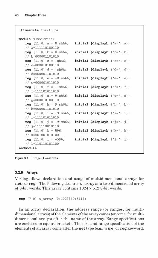
3.2.8 Arrays
Verilog allows declaration and usage of multidimensional arrays fornets or regs. The following declares a_array as a two-dimensional arrayof 8-bit words. This array contains 1024 × 512 8-bit words.
reg [7:0] a_array [0:1023][0:511];
In an array declaration, the address range (or ranges, for multi-dimensional arrays) of the elements of the array comes (or come, for multi-dimensional arrays) after the name of the array. Range specificationsare enclosed in square brackets. The size and range specification of theelements of an array come after the net type (e.g., wire) or reg keyword.
46 Chapter Three
`timescale 1ns/100ps
module NumberTest;reg [11:0] a = 8’shA6; initial $displayb (“a=”, a); // a=111110100110reg [11:0] b = 8’sh6A; initial $displayb (“b=”, b); // b=000001101010reg [11:0] c = ‘shA6; initial $displayb (“c=”, c);// c=000010100110reg [11:0] d = ‘sh6A; initial $displayb (“d=”, d);// d=000001101010reg [11:0] e = -8’shA6; initial $displayb (“e=”, e); // e=000001011010 reg [11:0] f = -’shA6; initial $displayb (“f=”, f); // f=111101011010reg [11:0] g = 9’shA6; initial $displayb (“g=”, g);// g=000010100110reg [11:0] h = 9’sh6A; initial $displayb (“h=”, h); // h=000001101010reg [11:0] i = -9’shA6; initial $displayb (“i=”, i); // i=111101011010reg [11:0] j = -9’sh6A; initial $displayb (“j=”, j);// j=111110010110reg [11:0] k = 596; initial $displayb (“k=”, k); // k=001001010100reg [11:0] l = -596; initial $displayb (“l=”, l); // l=110110101100
endmodule
Figure 3.7 Integer Constants
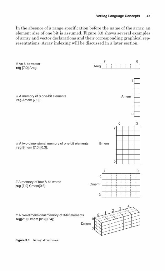
In the absence of a range specification before the name of the array, anelement size of one bit is assumed. Figure 3.8 shows several examplesof array and vector declarations and their corresponding graphical rep-resentations. Array indexing will be discussed in a later section.
Verilog Language Concepts 47
07
Areg
7
0
Amem
0
7
0
3
0
07
3
4
00
3
12
3
// An 8-bit vectorreg [7:0] Areg;
// A memory of 8 one-bit elementsreg Amem [7:0];
// A two-dimensional memory of one-bit elementsreg Bmem [7:0] [0:3];
// A memory of four 8-bit wordsreg [7:0] Cmem[0:3];
// A two-dimensional memory of 3-bit elementsreg[2:0] Dmem [0:3] [0:4];
Bmem
Cmem
Dmem
Figure 3.8 Array structures
3.2.9 Verilog operators
Boolean operations are the most common type of operations for describ-ing functions of hardware components at the gate or even RT level. Inaddition, there are operations for the behavioral or functional descriptionof hardware. Most operations found in software languages, are also sup-ported in Verilog. Figure 3.9 shows Verilog operators and a brief descrip-tion of each.
Operators in Fig. 3.9 are grouped according to their functionalities. Thefirst group is the basic operators for arithmetic and relational operations.These operations are very similar to those found in software languages.The next group shows equality operators. An equality operator returnsa 1 or 0 resulting from comparison of its operators. The next group showsboolean operators that are used for formation of conditions and for bit-wise logical operations. Various shift operations constitute the next groupof operators. Concatenation and replication operators are listed next inthe table of Fig. 3.9. In the last part of this figure the conditional oper-ation is shown. In the discussions that follow, after describing a groupof operators, several simple examples will be given.
3.2.9.1 Basic operators. Arithmetic operators in Verilog take bit, vector,integer, and real operands. These operators that are +, −, *, /, and **,result in multi-bit vectors. For the multiply operation, the size of theresult is determined by adding the bit lengths of the two operands. Forthe other arithmetic operations, the size of the result is the maximumof the bit lengths of the operands. An X or a Z value in a bit of either ofthe operands causes the entire result of the multiply operation to becomeunknown X.
Unary plus (+) and minus (−) are allowed in Verilog. These operatorstake precedence over other arithmetic operators.
The modulus operation (%) results in the remainder of its first operandwhen divided by its second operand. The sign of the result of a modu-lus expression takes the sign of its first operand.
An expression using a relational operator results in a 0 if the speci-fied relation is false or 1 if it is true. If any of the operands of a relationaloperator contain an X or a Z, then the result becomes X. When twovector operands of unequal bit lengths are being compared, the smalleroperand will be zero filled on the left to become the same size as thelarger-length operand. Several examples of basic operators are shownin Table 3.2.
3.2.9.2 Equality operators. Equality operators are categorized into twogroups of logical and case. The logical group compare their operands forequality (==) or inequality (!=), and return a one-bit result, 0, 1, or X.An X ambiguity arises when an X or a Z occurs in one of the operands.
48 Chapter Three
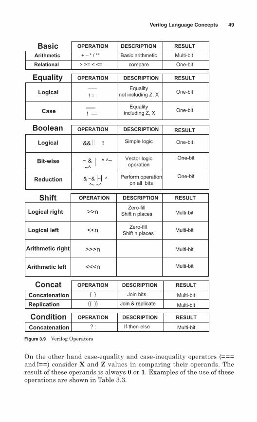
On the other hand case-equality and case-inequality operators (===and !==) consider X and Z values in comparing their operands. Theresult of these operands is always 0 or 1. Examples of the use of theseoperations are shown in Table 3.3.
Verilog Language Concepts 49
Figure 3.9 Verilog Operators
Basic OPERATION DESCRIPTION RESULT
Relational
Arithmetic
OPERATION DESCRIPTION RESULT
Logical
Case
Equality
Boolean OPERATION DESCRIPTION RESULT
Logical
Bit-wise
Reduction
Concatenation
Replication
Concat
&& !
~ & ^ ^~ ~^
& ~& ~ ^^~ ~^
Simple logic
Vector logicoperation
Perform operation on all bits
One-bit
One-bit
One-bit
One-bit
One-bit
Equality not including Z, X
Equality including Z, X
! =
!
Multi-bit
One-bitcompare
Basic arithmetic+ – * / **
> >= < <=
Logical right
Logical left
Arithmetic right
Arithmetic left
OPERATION DESCRIPTION RESULTShift
>>n
<<n
>>>n
<<<n
Zero-fillShift n places
Zero-fillShift n places
Multi-bit
Multi-bit
Multi-bit
Multi-bit
RESULT
Multi-bit
Multi-bit
OPERATION DESCRIPTION
{ }
{{ }}
Join bits
Join & replicate
Concatenation
Condition RESULT
Multi-bit
OPERATION DESCRIPTION
? : If-then-else
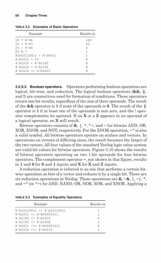
3.2.9.3 Boolean operators. Operators performing boolean operations arelogical, bit-wise, and reduction. The logical boolean operators (&&, ||,and !) are connectives used for formation of conditions. These operatorsreturn one bit results, regardless of the size of their operands. The resultof the && operator is 1 if none of the operands is 0. The result of the ||operator is 1 if at least one of the operands is non zero, and the ! oper-ator complements its operand. If an X or a Z appears in an operand ofa logical operator, an X will result.
Bitwise operators consists of &, |, ^, ^~, and ~ for bitwise AND, OR,XOR, XNOR, and NOT, respectively. For the XNOR operation, ~^ is alsoa valid symbol. All bitwise operators operate on scalars and vectors. Inoperations on vectors of differing sizes, the result becomes the larger ofthe two vectors. All four values of the standard Verilog logic value systemare valid bit values for bitwise operators. Figure 3.10 shows the resultsof bitwise operators operating on two 1-bit operands for four bitwiseoperators. The complement operator ~, not shown in this figure, resultsin 1 and 0 for 0 and 1 inputs and X for X and Z inputs.
A reduction operation is referred to as one that performs a certain bit-wise operation on bits of a vector and reduces it by a single bit. There aresix reduction operations in Verilog. These operations are &, ~&, |, ~|, ^,and ~^ (or ^~) for AND, NAND, OR, NOR, XOR, and XNOR. Applying a
50 Chapter Three
TABLE 3.2 Examples of Basic Operators
Example Results in
25 * 8’b6 15025 + 8’b7 3225 / 8’b6 422 % 7 181b10110011 > 8’b0011 14’b1011 < 10 04’b1Z10 < 4’b1100 X4’b1x10 < 4’b1100 X4’b1x10 <= 4’b1x10 X
TABLE 3.3 Examples of Equality Operators
Example Results in
8’b10110011 == 8’b10110011 18’b1011 == 8’b00001011 14’b1100 == 4’b1Z10 04’b1100 != 8’b100X 18’b1011 !== 8’b00001011 08’b101X === 8’b101X 1
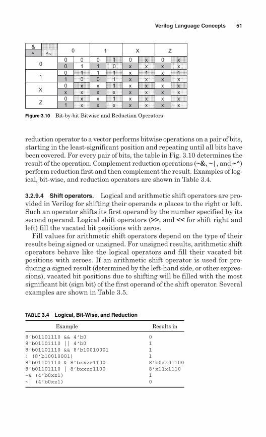
reduction operator to a vector performs bitwise operations on a pair of bits,starting in the least-significant position and repeating until all bits havebeen covered. For every pair of bits, the table in Fig. 3.10 determines theresult of the operation. Complement reduction operations (~&, ~|, and ~^)perform reduction first and then complement the result. Examples of log-ical, bit-wise, and reduction operators are shown in Table 3.4.
3.2.9.4 Shift operators. Logical and arithmetic shift operators are pro-vided in Verilog for shifting their operands n places to the right or left.Such an operator shifts its first operand by the number specified by itssecond operand. Logical shift operators (>>, and << for shift right andleft) fill the vacated bit positions with zeros.
Fill values for arithmetic shift operators depend on the type of theirresults being signed or unsigned. For unsigned results, arithmetic shiftoperators behave like the logical operators and fill their vacated bitpositions with zeroes. If an arithmetic shift operator is used for pro-ducing a signed result (determined by the left-hand side, or other expres-sions), vacated bit positions due to shifting will be filled with the mostsignificant bit (sign bit) of the first operand of the shift operator. Severalexamples are shown in Table 3.5.
Verilog Language Concepts 51
&
0^~^
00 1
0 0 0
0 1 x x
1 x x
1 1 1 11 x x
1 x0 x0
0
1
x
x x
x
0x01
xxxx
x xx
x x x
1 x x
xx1x
x
x
x
x
x
x
x
x
x
x
x
X
1
0
0 Z
Z
1
X
Figure 3.10 Bit-by-bit Bitwise and Reduction Operators
TABLE 3.4 Logical, Bit-Wise, and Reduction
Example Results in
8’b01101110 && 4’b0 08’b01101110 || 4’b0 18’b01101110 && 8’b10010001 1! (8’b10010001) 18’b01101110 & 8’bxxzz1100 8’b0xx011008’b01101110 | 8’bxxzz1100 8’x11x1110~& (4’b0xz1) 1~| (4’b0xz1) 0
3.2.9.5 Concatenation operators. An important operation in hardwaremodeling is concatenation. This operation is used for formation of vec-tored sources or destinations from smaller vectors or scalars. The nota-tion used for this operator is a pair of curly brackets ({...}) enclosing allscalars and vectors that are being concatenated.
The concatenation operator may be used on the left-hand side of anassignment. For example, if a is a 4-bit reg and aa is a 6-bit reg, the fol-lowing assignment places 1101 in a and 001001 in aa:
{a, aa} = 10’b1101001001
A concatenation operation on the right-hand side forms a vector of thesize of all the variables that are being concatenated. This vector may beused in other operations or can be assigned to a left-hand side target.
A repetition multiplier can be used to form a vector. This vector maybe used in another concatenation operation, or may be used as a vectorin other operations, or as a right-hand side assignment. If the a and aavariables have the values assigned to them above, and aaa is a 16-bitreg data type, then the assignment,
aaa = {aa, {2{a}}, 2’b11}
puts 001001_1101_1101_11 in aaa. The leftmost 6 bits come from aa,the next 8 bits are two times repetition of a, and the least-significant2 bits are the 2-bit constant 11. Below are more examples of concate-nation and replication operators:
{a, 2{b,c}, 3{d} is equivalent to: {a,b,c,b,c,d,d,d}{2’b00, 3{2’01}, 2’b’11} results in: 10’b0001010111
3.2.9.6 Conditional operator. The conditional operator in Verilog usesthe ?: notation, the general format of this operation is:
expression1 ? expression2 : expression3
If expression1 is true, then expression2 is selected as the result of theoperation; otherwise expression3 is selected. This operation provides a
52 Chapter Three
TABLE 3.5 Shift Operators
Example Results in
8’b0110_0111<<3 8’b0011-10008’b0110_0111<<1’bz 8’bxxxx-xxxxSigned_LHS = 8’b1100-0000>>>2 8’b1111-0000
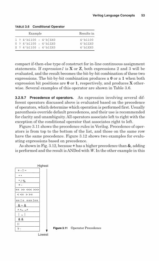
compact if-then-else type of construct for in-line continuous assignmentstatements. If expression1 is X or Z, both expressions 2 and 3 will beevaluated, and the result becomes the bit-by-bit combination of these twoexpressions. The bit-by-bit combination produces a 0 or a 1 when bothexpression bit positions are 0 or 1, respectively, and produces X other-wise. Several examples of this operator are shown in Table 3.6.
3.2.9.7 Precedence of operators. An expression involving several dif-ferent operators discussed above is evaluated based on the precedenceof operators, which determine which operation is performed first. Usuallyparenthesis override default precedences, and their use is recommendedfor clarity and unambiguity. All operators associate left to right with theexception of the conditional operator that associates right to left.
Figure 3.11 shows the precedence rules in Verilog. Precedence of oper-ators is from top to the bottom of the list, and those on the same rowhave the same precedence. Figure 3.12 shows two examples for evalu-ating expressions based on precedence.
As shown in Fig. 3.12, because + has a higher precedence than &, addingis performed and the result is ANDed with W. In the other example in this
Verilog Language Concepts 53
TABLE 3.6 Conditional Operator
Example Results in
1 ? 4’b1100 : 4’b|ZX0 4’b11000 ? 4’b1100 : 4’b1ZX0 4’b1ZX0X ? 4’b1100 : 4’b1ZX0 4’b1XX0
+ - ! ~
* *
* / %+ -
<< >> <<< >>>
< <= > >=
== ! = === !==
& ~ &
^ ^~ ~^
~
& &
? :
Highest
Lowest
Figure 3.11 Operator Precedence
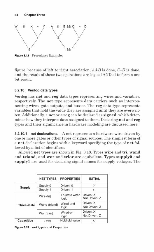
figure, because of left to right association, A&B is done, C+D is done,and the result of these two operations are logical ANDed to form a onebit result.
3.2.10 Verilog data types
Verilog has net and reg data types representing wires and variables,respectively. The net type represents data carriers such as intercon-necting wires, gate outputs, and busses. The reg data type representsvariables that hold the value they are assigned until they are overwrit-ten. Additionally, a net or a reg can be declared as signed, which deter-mines how they interpret data assigned to them. Declaring net and regtypes and their significance in hardware modeling are discussed here.
3.2.10.1 net declarations. A net represents a hardware wire driven byone or more gates or other types of signal sources. The simplest form ofa net declaration begins with a keyword specifying the type of net fol-lowed by a list of identifiers.
Allowed net types are shown in Fig. 3.13. Types wire and tri, wandand triand, and wor and trior are equivalent. Types supply0 andsupply1 are used for declaring signal names for supply voltages. The
54 Chapter Three
W X + Y
+
&
+&
&&
A & B D+&& C&
Figure 3.12 Precedence Examples
NET TYPES PROPERTIES INITIAL
0
1
Driven: XNot Driven: Z
Not Driven: Z
Driven: X
Driven: X
Not Driven: Z
X
Driven: 0
Driven: 1
Tri-state wiredlogic
Wired-andlogic
Wired-orlogic
Hold old value
Supply 0
Supply 1
Wire (tri)
Wand (triand)
Wor (trior)
trireg
Supply
Three-state
Capacitive
Figure 3.13 net types and Properties
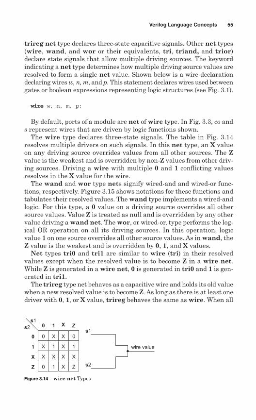
trireg net type declares three-state capacitive signals. Other net types(wire, wand, and wor or their equivalents, tri, triand, and trior)declare state signals that allow multiple driving sources. The keywordindicating a net type determines how multiple driving source values areresolved to form a single net value. Shown below is a wire declarationdeclaring wires w, n, m, and p. This statement declares wires used betweengates or boolean expressions representing logic structures (see Fig. 3.1).
wire w, n, m, p;
By default, ports of a module are net of wire type. In Fig. 3.3, co ands represent wires that are driven by logic functions shown.
The wire type declares three-state signals. The table in Fig. 3.14resolves multiple drivers on such signals. In this net type, an X valueon any driving source overrides values from all other sources. The Zvalue is the weakest and is overridden by non-Z values from other driv-ing sources. Driving a wire with multiple 0 and 1 conflicting valuesresolves in the X value for the wire.
The wand and wor type nets signify wired-and and wired-or func-tions, respectively. Figure 3.15 shows notations for these functions andtabulates their resolved values. The wand type implements a wired-andlogic. For this type, a 0 value on a driving source overrides all othersource values. Value Z is treated as null and is overridden by any othervalue driving a wand net. The wor, or wired-or, type performs the log-ical OR operation on all its driving sources. In this operation, logicvalue 1 on one source overrides all other source values. As in wand, theZ value is the weakest and is overridden by 0, 1, and X values.
Net types tri0 and tri1 are similar to wire (tri) in their resolvedvalues except when the resolved value is to become Z in a wire net.While Z is generated in a wire net, 0 is generated in tri0 and 1 is gen-erated in tri1.
The trireg type net behaves as a capacitive wire and holds its old valuewhen a new resolved value is to become Z. As long as there is at least onedriver with 0, 1, or X value, trireg behaves the same as wire. When all
Verilog Language Concepts 55
s1
s2
wire value
s1
s2 0 1 Z
0
1
X
Z
0 X 0
X
X
0
1
X X
X
X
Z
X
X
X
1
1
Figure 3.14 wire net Types
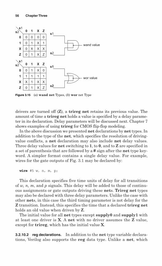
drivers are turned off (Z), a trireg net retains its previous value. Theamount of time a trireg net holds a value is specified by a delay parame-ter in its declaration. Delay parameters will be discussed next. Chapter 7shows examples of using trireg for CMOS flip-flop modeling.
In the above discussion we presented net declarations by net types. Inaddition to the type of the net, which specifies the resolution of driving-value conflicts, a net declaration may also include net delay values.Three delay values for net switching to 1, to 0, and to Z are specified ina set of parenthesis that are followed by a # sign after the net type key-word. A simpler format contains a single delay value. For example,wires for the gate outputs of Fig. 3.1 may be declared by:
wire #5 w, n, m, p;
This declaration specifies five time units of delay for all transitionsof w, n, m, and p signals. This delay will be added to those of continu-ous assignments or gate outputs driving these nets. Trireg net typesmay also be declared with three delay parameters. Unlike the case withother nets, in this case the third timing parameter is not delay for theZ transition. Instead, this specifies the time that a declared trireg netholds an old value when driven by Z.
The initial value for all net types except supply0 and supply1 withat least one driver is X. A net with no driver assumes the Z value,except for trireg, which has the initial value X.
3.2.10.2 reg declarations. In addition to the net type variable declara-tions, Verilog also supports the reg data type. Unlike a net, which
56 Chapter Three
wand value
s1
s1
s2
s2
s1s2 0 1 Z
0
1
X
Z
0 0 0
0
0
0
1
X X
X
X
Z
s1s2 0 1 Z
0
1
X
Z
0 0
1
X
0
1
1 X
X
1
Z
X
0
1
X
1
X
1 X
1
X
1
wor value
Figure 3.15 (a) wand net Types, (b) wor net Type
models an interconnection or a gate output, a reg is a variable for hold-ing intermediate signal values or nonhardware parameters and func-tion values. The reg declaration shown below declares a, b, and ci as regtypes with 0 initial values.
reg a = 0, b = 0, ci = 0;
This declaration is used in the FulladderTester module of Fig. 3.4 forassigning test values to the ports of the instantiated Full_adder module.
Because reg variables are not used exclusively for hardware model-ing, other reg type declarations for more convenient forms of modelparameters are provided in Verilog. These reg types are integer andtime. An integer declaration declares a signed 2s-complement number,and a time declaration declares an unsigned reg variable of at least64 bits. Verilog also allows declaration of real and realtime variables.These variables are similar in use to integer and time variables, butdo not have direct bit-to-bit correspondence with reg type registers.The default initial value of a declared reg is (X). As shown in Fig. 3.4,this default can be overwritten when a reg is being declared.
3.2.10.3 Signed data. Verilog net and reg types can be declared assigned. Integer declaration is always considered signed. A signed 16-bitreg declaration is done as shown here:
reg signed [15:0] areg;
An expression using variables, nets, and constants as operand canbecome signed or unsigned depending on its operands. The left-hand sideof an expression does not have any effect on the sign of the expression.A signed reg that is shifted right by the >>> operator is sign filled,whereas an unsigned reg shifted by this operator is zerofilled.
Integers are signed, and based numbers with the s notation are alsosigned. Other vector constants are considered unsigned. Concatenationand vector slicing always result in unsigned results. For other operatorsto result in signed results, all operands must be signed.
If the right-hand side of an assignment is determined as signed, it issign extended to the size of its left-hand side and is placed on the left-hand side reg or net. As mentioned before, the extension of the sign onlydepends on the right-hand side and not on the left-hand side reg or net.
3.2.10.4 Parameters. Parameters in Verilog do not belong to either thevariable or the net group. Parameters are constants and cannot be changedat runtime. Parameters can be declared as signed, real, integer, time,or realtime. Shown in Table 3.7 are several parameter declarations.
Verilog Language Concepts 57
3.2.11 Array indexing
Bit-select and part-select operators are used for extracting a bit or agroup of bits from a declared array. Such addressing only applies tocontiguous bits of an array. We use arrays of Sec. 3.2.6 (Fig. 3.8) todemonstrate bit-select and part-select operations. These arrays areshown here for reference.
reg [7:0] Areg;reg Amem [7:0];reg Dmem [7:0][0:3];reg [7:0] Cmem [0:3];reg [2:0] Dmem [0:3][0:4];
3.2.11.1 Bit selection. Bit-selection is done by using the addressed bitnumber in a set of square brackets. For example Areg[5] selects bit 5 ofthe Areg array.
3.2.11.2 Part selection. Verilog allows constant and indexed part-select.A constant part-select specifies range of bits to be selected. For exam-ple, Areg[7:3] selects the upper five bits of Areg. On the other hand anindexed part-select specifies starting index and the number of bits to beselected. For example, Areg[3+:5] selects the same five bits as Areg[7:3]does. Several examples follow:
Areg [5:3] selects bits 5, 4, and 3Areg [5-:4] selects bits 5, 4, 3, and 2Areg [2+:4] selects bits 5, 4, 3, and 2
3.2.11.3 Standard memory. The standard format for declaring a memoryin Verilog is to declare it as an array of a vector. For example Cmem, asshown above, is a 4-word memory of 8-bit words. The address space ofthis memory is 4. Emem as a byte-oriented memory of with a 10 bitaddress (1024 address space) is declared as:
reg [7:0] Emem [0:1023];
58 Chapter Three
TABLE 3.7 Parameter Examples
Example Explanation
parameter p1=5, p2=6; 32 bit parametersparameter [4:0] p1=5, p2=6; 5 bit parameters parameter integer p1=5; 32 bit parameterparameter signed [4:0] p1=5; 5 bit signed parameter
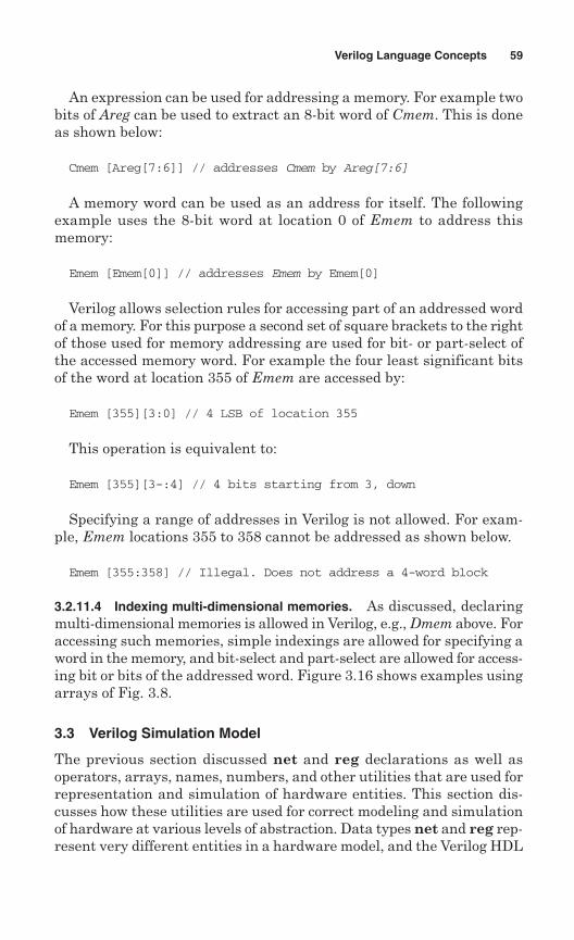
An expression can be used for addressing a memory. For example twobits of Areg can be used to extract an 8-bit word of Cmem. This is doneas shown below:
Cmem [Areg[7:6]] // addresses Cmem by Areg[7:6]
A memory word can be used as an address for itself. The followingexample uses the 8-bit word at location 0 of Emem to address thismemory:
Emem [Emem[0]] // addresses Emem by Emem[0]
Verilog allows selection rules for accessing part of an addressed wordof a memory. For this purpose a second set of square brackets to the rightof those used for memory addressing are used for bit- or part-select ofthe accessed memory word. For example the four least significant bitsof the word at location 355 of Emem are accessed by:
Emem [355][3:0] // 4 LSB of location 355
This operation is equivalent to:
Emem [355][3-:4] // 4 bits starting from 3, down
Specifying a range of addresses in Verilog is not allowed. For exam-ple, Emem locations 355 to 358 cannot be addressed as shown below.
Emem [355:358] // Illegal. Does not address a 4-word block
3.2.11.4 Indexing multi-dimensional memories. As discussed, declaringmulti-dimensional memories is allowed in Verilog, e.g., Dmem above. Foraccessing such memories, simple indexings are allowed for specifying aword in the memory, and bit-select and part-select are allowed for access-ing bit or bits of the addressed word. Figure 3.16 shows examples usingarrays of Fig. 3.8.
3.3 Verilog Simulation Model
The previous section discussed net and reg declarations as well asoperators, arrays, names, numbers, and other utilities that are used forrepresentation and simulation of hardware entities. This section dis-cusses how these utilities are used for correct modeling and simulationof hardware at various levels of abstraction. Data types net and reg rep-resent very different entities in a hardware model, and the Verilog HDL
Verilog Language Concepts 59
is very specific as to the way they are used and the language constructsthey are used in. We will show semantics of assignments to reg and netdata types.
Variables declared as net are assigned values in Verilog concurrentbodies using continuous assignment statements. On the other hand,reg variables are assigned values in procedural bodies. The followingdiscusses details of these constructs.
60 Chapter Three
07
Areg
7
0
Amem
0
7
0
3
0
07
3
// declaration: reg [7:0] Areg;Areg [7:5]
// declaration: reg Amem [7:0];Amem [3]
// declaration: reg Bmem [7:0][0:3]Bmem [2] [1]
// declaration: reg[7:0] Cmem [0:3]Cmem [1] [6 -: 4]
// declaration: reg [2:0] Dmem [0:3][0:4]Dmem [0] [2]
Bmem
Cmem
Dmem
3
0
01
23
4
Figure 3.16 Array Addressing and Selection
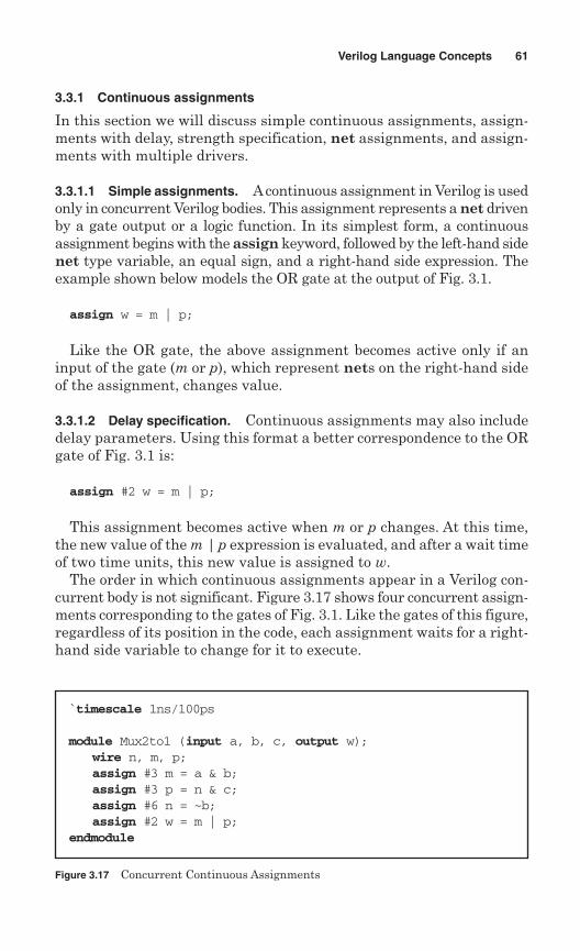
3.3.1 Continuous assignments
In this section we will discuss simple continuous assignments, assign-ments with delay, strength specification, net assignments, and assign-ments with multiple drivers.
3.3.1.1 Simple assignments. Acontinuous assignment in Verilog is usedonly in concurrent Verilog bodies. This assignment represents a net drivenby a gate output or a logic function. In its simplest form, a continuousassignment begins with the assign keyword, followed by the left-hand sidenet type variable, an equal sign, and a right-hand side expression. Theexample shown below models the OR gate at the output of Fig. 3.1.
assign w = m | p;
Like the OR gate, the above assignment becomes active only if aninput of the gate (m or p), which represent nets on the right-hand sideof the assignment, changes value.
3.3.1.2 Delay specification. Continuous assignments may also includedelay parameters. Using this format a better correspondence to the ORgate of Fig. 3.1 is:
assign #2 w = m | p;
This assignment becomes active when m or p changes. At this time,the new value of the m | p expression is evaluated, and after a wait timeof two time units, this new value is assigned to w.
The order in which continuous assignments appear in a Verilog con-current body is not significant. Figure 3.17 shows four concurrent assign-ments corresponding to the gates of Fig. 3.1. Like the gates of this figure,regardless of its position in the code, each assignment waits for a right-hand side variable to change for it to execute.
Verilog Language Concepts 61
`timescale 1ns/100ps
module Mux2to1 (input a, b, c, output w);wire n, m, p;assign #3 m = a & b;assign #3 p = n & c;assign #6 n = ~b;assign #2 w = m | p;
endmodule
Figure 3.17 Concurrent Continuous Assignments
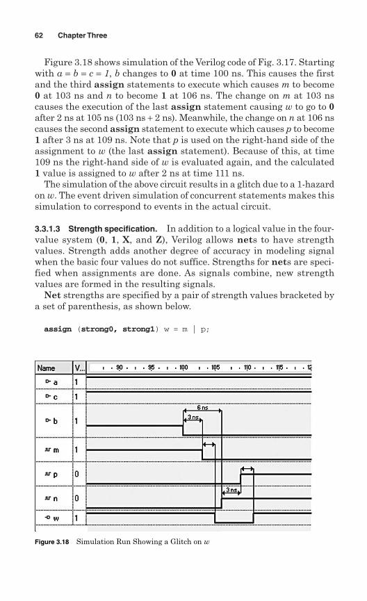
Figure 3.18 shows simulation of the Verilog code of Fig. 3.17. Startingwith a = b = c = 1, b changes to 0 at time 100 ns. This causes the firstand the third assign statements to execute which causes m to become0 at 103 ns and n to become 1 at 106 ns. The change on m at 103 nscauses the execution of the last assign statement causing w to go to 0after 2 ns at 105 ns (103 ns + 2 ns). Meanwhile, the change on n at 106 nscauses the second assign statement to execute which causes p to become1 after 3 ns at 109 ns. Note that p is used on the right-hand side of theassignment to w (the last assign statement). Because of this, at time109 ns the right-hand side of w is evaluated again, and the calculated1 value is assigned to w after 2 ns at time 111 ns.
The simulation of the above circuit results in a glitch due to a 1-hazardon w. The event driven simulation of concurrent statements makes thissimulation to correspond to events in the actual circuit.
3.3.1.3 Strength specification. In addition to a logical value in the four-value system (0, 1, X, and Z), Verilog allows nets to have strengthvalues. Strength adds another degree of accuracy in modeling signalwhen the basic four values do not suffice. Strengths for nets are speci-fied when assignments are done. As signals combine, new strengthvalues are formed in the resulting signals.
Net strengths are specified by a pair of strength values bracketed bya set of parenthesis, as shown below.
assign (strong0, strong1) w = m | p;
62 Chapter Three
Figure 3.18 Simulation Run Showing a Glitch on w
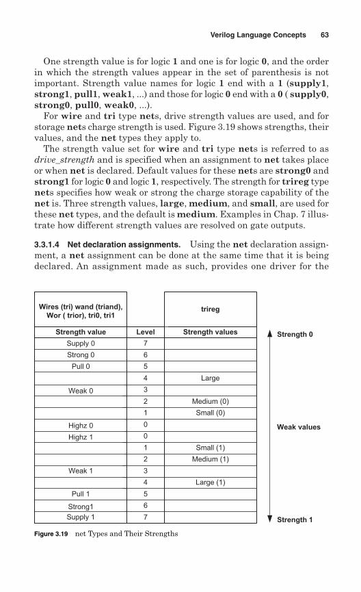
One strength value is for logic 1 and one is for logic 0, and the orderin which the strength values appear in the set of parenthesis is notimportant. Strength value names for logic 1 end with a 1 (supply1,strong1, pull1, weak1, ...) and those for logic 0 end with a 0 ( supply0,strong0, pull0, weak0, ...).
For wire and tri type nets, drive strength values are used, and forstorage nets charge strength is used. Figure 3.19 shows strengths, theirvalues, and the net types they apply to.
The strength value set for wire and tri type nets is referred to asdrive_strength and is specified when an assignment to net takes placeor when net is declared. Default values for these nets are strong0 andstrong1 for logic 0 and logic 1, respectively. The strength for trireg typenets specifies how weak or strong the charge storage capability of thenet is. Three strength values, large, medium, and small, are used forthese net types, and the default is medium. Examples in Chap. 7 illus-trate how different strength values are resolved on gate outputs.
3.3.1.4 Net declaration assignments. Using the net declaration assign-ment, a net assignment can be done at the same time that it is beingdeclared. An assignment made as such, provides one driver for the
Verilog Language Concepts 63
Wires (tri) wand (triand),
Wor ( trior), tri0, tri1
Strength value
Supply 0
Strong 0
Pull 0
Weak 0
Highz 0
Highz 1
Weak 1
Pull 1
Strong1
Supply 1
trireg
Level Strength values
7
6
5
4
3
2
1
0
0
1
2
3
4
5
6
7
Large
Medium (0)
Small (0)
Small (1)
Medium (1)
Large (1)
Strength 0
Strength 1
Weak values
Figure 3.19 net Types and Their Strengths
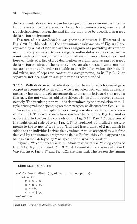
declared net. More drivers can be assigned to the same net using con-tinuous assignment statements. As with continuous assignments andnet declarations, strengths and timing may also be specified in a netdeclaration assignment.
The use of net_declaration_assignment construct is illustrated inFig. 3.20. In this code, all the continuous assignments of Fig. 3.17 arereplaced by a list of net declaration assignments providing drivers forw, n, m, and p signals. Drive strengths and/or delay values specified ina net declaration assignment apply to all net drivers. The syntax usedhere consists of a list of net declaration assignments as part of a netdeclaration construct. The same syntax can also be used with continu-ous assignments. In order to be able to specify delay values for individ-ual wires, use of separate continuous assignments, as in Fig. 3.17, orseparate net declaration assignments is recommended.
3.3.1.5 Multiple drivers. A situation in hardware in which several gateoutput are connected to the same wire is modeled with continuous assign-ments by having multiple assignments to the same left-hand side net. Inthis case, the net value is said to be driven with multiple sources simulta-neously. The resulting net value is determined by the resolution of mul-tiple driving values depending on the net types, as discussed in Sec. 3.2.10.
An example for multiple drivers using wired-or resolution is shownin Fig. 3.21. The code shown here models the circuit of Fig. 3.1 and isequivalent to the Verilog code shown in Fig. 3.17. The OR operation ofthe right-hand side of w in Fig. 3.17 is replaced by multiple assign-ments to the w net of wor type. This net has a delay of 2 ns, which isadded to the individual driver delay values. A value assigned to w is firstdelayed by continuous assignment delay. Before this value appears onw, it is further delayed by 2 ns specified in wor declaration.
Figure 3.22 compares the simulation results of the Verilog codes ofFig. 3.17, Fig. 3.20, and Fig. 3.21. All simulations are event based.Waveforms of Fig. 3.17 and Fig. 3.21 are identical. The reason the timing
64 Chapter Three
`timescale 1ns/100ps
module Mux2to1Net (input a, b, c, output w);wire #3m = a & b, p = n & c,n = ~b,w = m | p;
endmodule
Figure 3.20 Using net_declaration_assignment
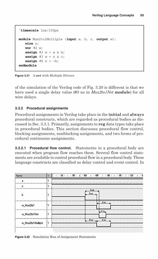
of the simulation of the Verilog code of Fig. 3.20 is different is that wehave used a single delay value (#3 ns in Mux2to1Net module) for allwire delays.
3.3.2 Procedural assignments
Procedural assignments in Verilog take place in the initial and alwaysprocedural constructs, which are regarded as procedural bodies as dis-cussed in Sec. 3.3.1. Primarily, assignments to reg data types take placein procedural bodies. This section discusses procedural flow control,blocking assignments, nonblocking assignments, and two forms of pro-cedural continuous assignments.
3.3.2.1 Procedural flow control. Statements in a procedural body areexecuted when program flow reaches them. Several flow control state-ments are available to control procedural flow in a procedural body. Theselanguage constructs are classified as delay control and event control. In
Verilog Language Concepts 65
`timescale 1ns/100ps
module Mux2to1Multiple (input a, b, c, output w);wire n;wor #2 w;assign #3 w = a & b;assign #3 w = n & c;assign #6 n = ~b;
endmodule
Figure 3.21 A net with Multiple Drivers
Figure 3.22 Simulation Run of Assignment Statements
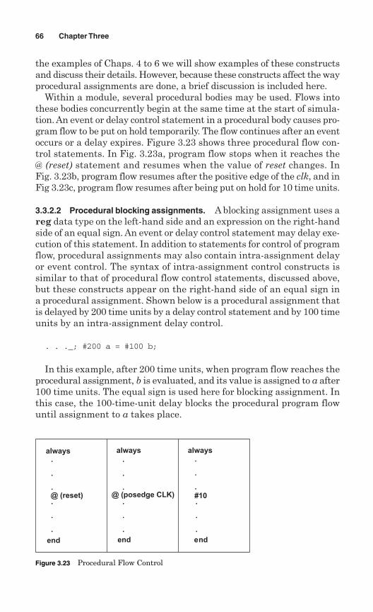
the examples of Chaps. 4 to 6 we will show examples of these constructsand discuss their details. However, because these constructs affect the wayprocedural assignments are done, a brief discussion is included here.
Within a module, several procedural bodies may be used. Flows intothese bodies concurrently begin at the same time at the start of simula-tion. An event or delay control statement in a procedural body causes pro-gram flow to be put on hold temporarily. The flow continues after an eventoccurs or a delay expires. Figure 3.23 shows three procedural flow con-trol statements. In Fig. 3.23a, program flow stops when it reaches the@ (reset) statement and resumes when the value of reset changes. InFig. 3.23b, program flow resumes after the positive edge of the clk, and inFig 3.23c, program flow resumes after being put on hold for 10 time units.
3.3.2.2 Procedural blocking assignments. A blocking assignment uses areg data type on the left-hand side and an expression on the right-handside of an equal sign. An event or delay control statement may delay exe-cution of this statement. In addition to statements for control of programflow, procedural assignments may also contain intra-assignment delayor event control. The syntax of intra-assignment control constructs issimilar to that of procedural flow control statements, discussed above,but these constructs appear on the right-hand side of an equal sign ina procedural assignment. Shown below is a procedural assignment thatis delayed by 200 time units by a delay control statement and by 100 timeunits by an intra-assignment delay control.
. . ._; #200 a = #100 b;
In this example, after 200 time units, when program flow reaches theprocedural assignment, b is evaluated, and its value is assigned to a after100 time units. The equal sign is used here for blocking assignment. Inthis case, the 100-time-unit delay blocks the procedural program flowuntil assignment to a takes place.
66 Chapter Three
always.
.
.@ (reset).
.
.
end
always always
.
.
.
.
.
.
.
.
.
.
.
.
end end
#10@ (posedge CLK)
Figure 3.23 Procedural Flow Control
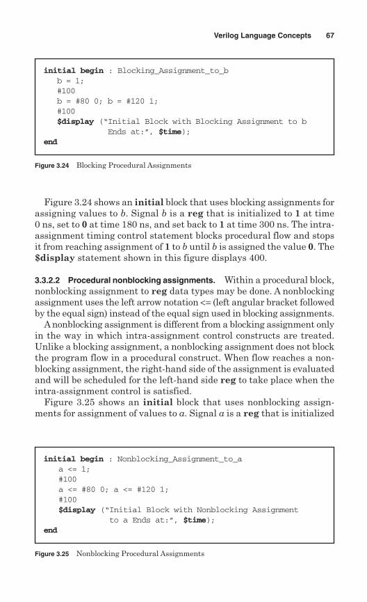
Figure 3.24 shows an initial block that uses blocking assignments forassigning values to b. Signal b is a reg that is initialized to 1 at time0 ns, set to 0 at time 180 ns, and set back to 1 at time 300 ns. The intra-assignment timing control statement blocks procedural flow and stopsit from reaching assignment of 1 to b until b is assigned the value 0. The$display statement shown in this figure displays 400.
3.3.2.2 Procedural nonblocking assignments. Within a procedural block,nonblocking assignment to reg data types may be done. A nonblockingassignment uses the left arrow notation <= (left angular bracket followedby the equal sign) instead of the equal sign used in blocking assignments.
A nonblocking assignment is different from a blocking assignment onlyin the way in which intra-assignment control constructs are treated.Unlike a blocking assignment, a nonblocking assignment does not blockthe program flow in a procedural construct. When flow reaches a non-blocking assignment, the right-hand side of the assignment is evaluatedand will be scheduled for the left-hand side reg to take place when theintra-assignment control is satisfied.
Figure 3.25 shows an initial block that uses nonblocking assign-ments for assignment of values to a. Signal a is a reg that is initialized
Verilog Language Concepts 67
initial begin : Blocking_Assignment_to_bb = 1;#100b = #80 0; b = #120 1;#100$display (“Initial Block with Blocking Assignment to b
Ends at:”, $time);end
Figure 3.24 Blocking Procedural Assignments
initial begin : Nonblocking_Assignment_to_aa <= 1;#100a <= #80 0; a <= #120 1;#100$display (“Initial Block with Nonblocking Assignment
to a Ends at:”, $time);end
Figure 3.25 Nonblocking Procedural Assignments
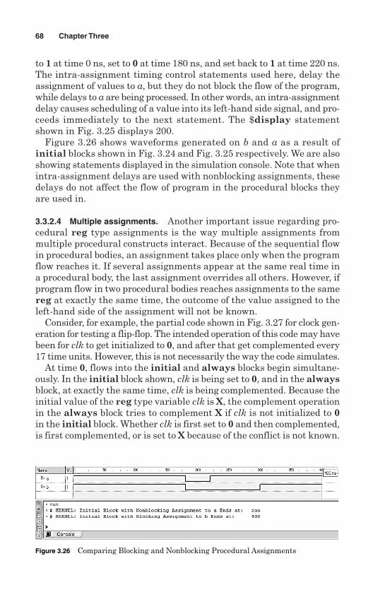
to 1 at time 0 ns, set to 0 at time 180 ns, and set back to 1 at time 220 ns.The intra-assignment timing control statements used here, delay theassignment of values to a, but they do not block the flow of the program,while delays to a are being processed. In other words, an intra-assignmentdelay causes scheduling of a value into its left-hand side signal, and pro-ceeds immediately to the next statement. The $display statementshown in Fig. 3.25 displays 200.
Figure 3.26 shows waveforms generated on b and a as a result ofinitial blocks shown in Fig. 3.24 and Fig. 3.25 respectively. We are alsoshowing statements displayed in the simulation console. Note that whenintra-assignment delays are used with nonblocking assignments, thesedelays do not affect the flow of program in the procedural blocks theyare used in.
3.3.2.4 Multiple assignments. Another important issue regarding pro-cedural reg type assignments is the way multiple assignments frommultiple procedural constructs interact. Because of the sequential flowin procedural bodies, an assignment takes place only when the programflow reaches it. If several assignments appear at the same real time ina procedural body, the last assignment overrides all others. However, ifprogram flow in two procedural bodies reaches assignments to the samereg at exactly the same time, the outcome of the value assigned to theleft-hand side of the assignment will not be known.
Consider, for example, the partial code shown in Fig. 3.27 for clock gen-eration for testing a flip-flop. The intended operation of this code may havebeen for clk to get initialized to 0, and after that get complemented every17 time units. However, this is not necessarily the way the code simulates.
At time 0, flows into the initial and always blocks begin simultane-ously. In the initial block shown, clk is being set to 0, and in the alwaysblock, at exactly the same time, clk is being complemented. Because theinitial value of the reg type variable clk is X, the complement operationin the always block tries to complement X if clk is not initialized to 0in the initial block. Whether clk is first set to 0 and then complemented,is first complemented, or is set to X because of the conflict is not known.
68 Chapter Three
Figure 3.26 Comparing Blocking and Nonblocking Procedural Assignments
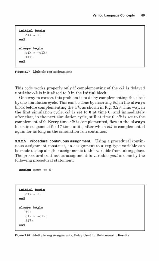
This code works properly only if complementing of the clk is delayeduntil the clk is initialized to 0 in the initial block.
One way to correct this problem is to delay complementing the clockby one simulation cycle. This can be done by inserting #0; in the alwaysblock before complementing the clk, as shown in Fig. 3.28. This way, inthe first simulation cycle, clk is set to 0 at time 0, and immediatelyafter that, in the next simulation cycle, still at time 0, clk is set to thecomplement of 0. Every time clk is complemented, flow in the alwaysblock is suspended for 17 time units, after which clk is complementedagain for as long as the simulation run continues.
3.3.2.5 Procedural continuous assignment. Using a procedural contin-uous assignment construct, an assignment to a reg type variable canbe made to stop all other assignments to this variable from taking place.The procedural continuous assignment to variable qout is done by thefollowing procedural statement:
assign qout <= 0;
Verilog Language Concepts 69
initial beginclk = 0;
end
always beginclk = ~clk;#17;
end
Figure 3.27 Multiple reg Assignments
initial beginclk = 0;
end
always begin#0;clk = ~clk;#17;
end
Figure 3.28 Multiple reg Assignments; Delay Used for Deterministic Results
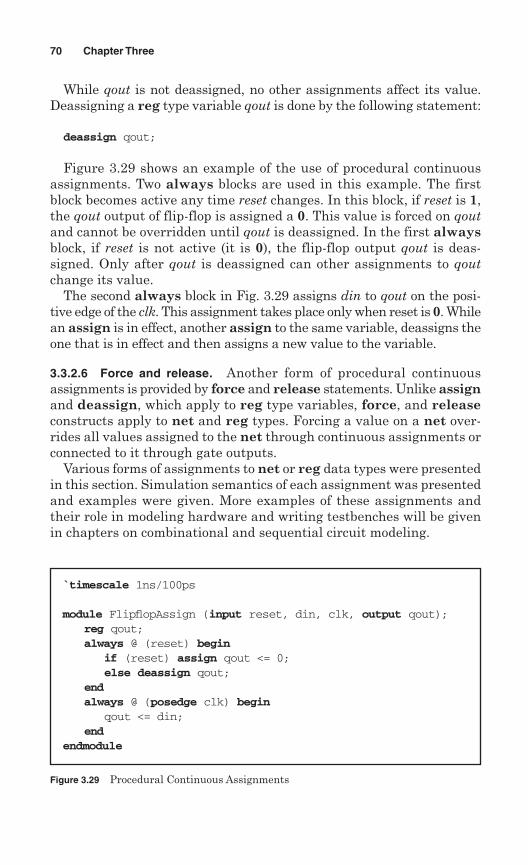
While qout is not deassigned, no other assignments affect its value.Deassigning a reg type variable qout is done by the following statement:
deassign qout;
Figure 3.29 shows an example of the use of procedural continuousassignments. Two always blocks are used in this example. The firstblock becomes active any time reset changes. In this block, if reset is 1,the qout output of flip-flop is assigned a 0. This value is forced on qoutand cannot be overridden until qout is deassigned. In the first alwaysblock, if reset is not active (it is 0), the flip-flop output qout is deas-signed. Only after qout is deassigned can other assignments to qoutchange its value.
The second always block in Fig. 3.29 assigns din to qout on the posi-tive edge of the clk. This assignment takes place only when reset is 0. Whilean assign is in effect, another assign to the same variable, deassigns theone that is in effect and then assigns a new value to the variable.
3.3.2.6 Force and release. Another form of procedural continuousassignments is provided by force and release statements. Unlike assignand deassign, which apply to reg type variables, force, and releaseconstructs apply to net and reg types. Forcing a value on a net over-rides all values assigned to the net through continuous assignments orconnected to it through gate outputs.
Various forms of assignments to net or reg data types were presentedin this section. Simulation semantics of each assignment was presentedand examples were given. More examples of these assignments andtheir role in modeling hardware and writing testbenches will be givenin chapters on combinational and sequential circuit modeling.
70 Chapter Three
`timescale 1ns/100ps
module FlipflopAssign (input reset, din, clk, output qout);reg qout;always @ (reset) begin
if (reset) assign qout <= 0;else deassign qout;
endalways @ (posedge clk) begin
qout <= din;end
endmodule
Figure 3.29 Procedural Continuous Assignments
3.4 Compiler Directives
Certain hardware modeling requirements in Verilog are provided ascompiler directives instead of being incorporated in the main syntaxof the language. Compiler directives provide facilities for file inclusion,timing specification, default settings, and string substitution. Thissection provides a brief description of these language facilities.Directives are presented in the order of their importance in hardwaremodeling.
3.4.1 `timescale
The `timescale directive sets the time unit and time precision in amodule. Including the
‘timescale 1ns/100ps
directive before a module header causes all time-related numbers to beinterpreted as having a 1ns time unit. When expressions manipulatingtiming values are performed, 100 ps precision will be used.
3.4.2 `default_nettype
Undeclared nets are implicitly declared as wire type nets. The defaultwire type can be changed by the `default_nettype. For example,
‘default_nettype wor
at the beginning of a module causes undeclared nets in constructs suchas the terminal list of a module instance to be assumed to be wor typenets.
This default setting stays in effect for all future compilations until itis set to another value or reset by use of the `resetall directive.
3.4.3 `include
To include a parameter definition file or a section of shared code in amodule, the `include directive may be used. Because Verilog does notprovide a common library of parts and utilities, a shared code must beexplicitly inserted in modules that use the code. This can be achievedusing the `include directive.
3.4.4 `define
For better code readability, a meaningful string (referred to as textmacro) can be defined to represent a number or an expression. The
Verilog Language Concepts 71
`define directives shown below define word_length of 32 and assignthe 101 binary code to state begin_fetch_state of a state machine.
`define word_length 32`define begin_fetch_state 3’b101
Defined strings may be used in Verilog code text by preceding theirdefined names by a back quote. For example, if ‘begin_fetch_state is usedanywhere in a Verilog code, it is replaced by 3’b101. The `undef direc-tive undefines a previously defined text macro.
3.4.5 `ifdef, `else, `endif
The ̀ ifdef directive tests whether a text macro that immediately followsthe `ifdef keyword has been defined using the `define directive. If thenext macro has been defined, the group of lines bracketed between`ifdef and ̀ else is compiled. If the text macro has not been defined, thegroup of lines bracketed between `else and `endif is compiled.
These directives can appear anywhere in a Verilog source code. Thetwo groups of lines bracketed in an `ifdef, `else, `endif structure mustindependently have correct syntax.
3.4.6 `unconnected_drive
A port value left open in the connection list of a module instantiationassumes the default net value. To change this and to force pull0 or pull1values on unconnected ports, the ̀ unconnected_drive directive can beused. The only arguments allowed with this directive are pull0 or pull1for unconnected values 0 and 1, respectively. The effect of this directivemay be turned off by `nounconnected_drive direction.
3.4.7 `celldefine, `endcelldefine
The `celldefine and `endcelldefine directives bracket modules thatare to be considered as cells. The Verilog programming language inter-face (PLI) uses cell modules.
3.4.8 `resetall
The ̀ resetall directive turns off the effect of all compiler directives. Usingthis directive at the beginning of every module guarantees that no pre-vious setting affects compilation of modules and that all defaults are set.
3.5 System Tasks and Functions
For testbench generation, data input and output, timing check, simu-lation flow control, data conversion, and memory initialization and
72 Chapter Three
specification, Verilog provides a number of system tasks and functionscategorized into ten groups. The names of system tasks and functionsbegin with a dollar sign ($), followed by a task specifier. The name of thetask or function usually contains characters and names that describe itsfunctionality. A brief description of these language utilities will be givenhere. Application of several of these tasks has already been presented inthis and the previous chapter, and more tasks and functions will be pre-sented in the examples that use them in the chapters that follow.
3.5.1 Display tasks
Display tasks are used for outputting to the standard output device. Themost basic display task is the $display task, which writes its stringargument to the display device. Other tasks include those for monitor-ing and outputting variable values as they change (the $monitor groupof tasks) and those for displaying variables at a selected time (the $dis-play tasks). Display tasks can display in binary, hexadecimal, or octalformats. The character b, h, or o at the end of the task name specifiesthe data type a task handles. For all display tasks, a generic task canbe used to display data with specified formats and data types. Chapteron testbenches presents examples that take advantage of many of thesetasks for outputting test results.
3.5.2 File I/O tasks
File output tasks begin with a dollar sign followed by the letter f (forfile) and then by the same task names as those of the display tasks.These tasks perform the same functionalities as their display task coun-terparts, except that their output is to a file instead of to the display ter-minal. The $fopen function opens a file and assigns an integer filedescription. The file descriptor will be used as an argument for all fileI/O tasks. In addition, there are string write tasks ($swrite) that writetheir formatted outputs to a string.
Verilog also provides tasks for inputting data from files or strings. Suchtasks allow reading characters, formatted data, or complete memory datafrom external data files or declared strings. Examples of these tasks are$fgetc, $fscanf, and $sscanf for getting a character from a file, readingformatted data from a file, and reading formatted data from a string,respectively. Other input tasks exist for reading memory data directly intoa declared memory. Examples of such tasks are $fread and $readmemh.
File positioning tasks, $fseek and $frewind are also available forpositioning file pointer for read or write.
Verilog I/O tasks are useful in developing complete hardware/softwareenvironments and developing testbenches. In the chapters that follow wewill use these tasks for developing testbenches and in conjunction with
Verilog Language Concepts 73
such applications, we will describe utilization of tasks. Appendix B hasa complete list of tasks and a simple example of each.
3.5.3 Timescale tasks
Timescale tasks are $printtimescale and $timeformat. The $print-timescale task displays the timescale and precision of the modulewhose hierarchical name is being passed to it as its argument. The$timeformat task formats time for display by file IO and display tasks.
3.5.4 Simulation control tasks
Simulation control tasks are $finish and $stop. The $finish task endsthe simulation and exits. Usually, simulation environments require aconfirmation before the action of exiting the environment is taken. The$stop task suspends the simulation and does not exit the simulationenvironment.
3.5.5 Timing check tasks
Timing check tasks are used for checking timings, such as pulse widthduration and setup and hold times. In general, timing check tasks checkthe timing on one signal or the relative timing of several signals for cer-tain conditions to hold. If a violation is detected, a message will beissued in the user simulation environment display area. For example,the statement shown below uses the $nochange timing check task toreport a violation if d_input changes in the period of three time unitsbefore and five time units after the positive edge of the clock.
$nochange (posedge clock, d_input, 3, 5);
3.5.6 PLA modeling tasks
Programmable logical array (PLA) modeling tools use a declaredmemory as their first argument, configure it as synchronous or asyn-chronous, assign inputs and outputs to the PLA array, and configure thelogical function of the PLA. Names used for PLA modeling tasks consistof three fields, sync_async, and_or, and array_plane. Tasks are namedusing these three fields separated by dollar signs. The general formatthat we use for describing these tasks is
$sync_async$and_or$array_plane
where sync_async can be either sync or async; and_or can be and, or,nand, or nor; and in place of array_plane, array or plane can be used.
74 Chapter Three
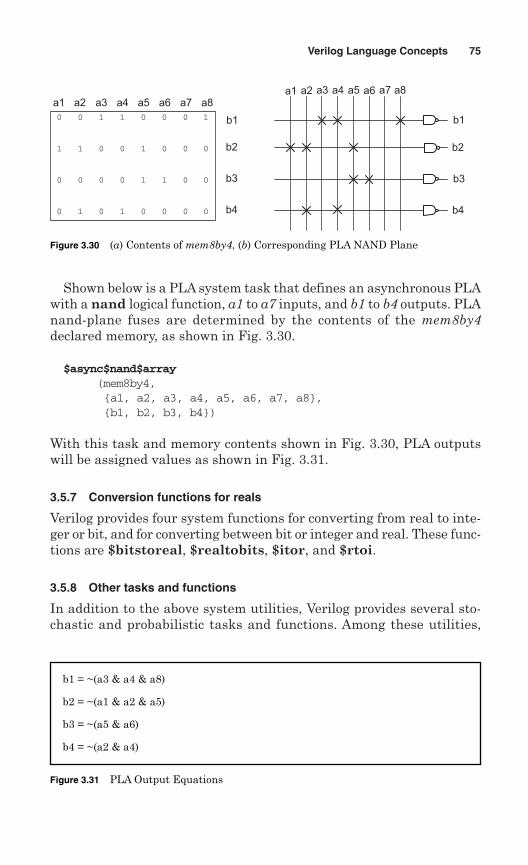
Shown below is a PLA system task that defines an asynchronous PLAwith a nand logical function, a1 to a7 inputs, and b1 to b4 outputs. PLAnand-plane fuses are determined by the contents of the mem8by4declared memory, as shown in Fig. 3.30.
$async$nand$array(mem8by4,{a1, a2, a3, a4, a5, a6, a7, a8},{b1, b2, b3, b4})
With this task and memory contents shown in Fig. 3.30, PLA outputswill be assigned values as shown in Fig. 3.31.
3.5.7 Conversion functions for reals
Verilog provides four system functions for converting from real to inte-ger or bit, and for converting between bit or integer and real. These func-tions are $bitstoreal, $realtobits, $itor, and $rtoi.
3.5.8 Other tasks and functions
In addition to the above system utilities, Verilog provides several sto-chastic and probabilistic tasks and functions. Among these utilities,
Verilog Language Concepts 75
b1
b2
b3
b4
b1
b2
b3
b4
a8a7a6a5a4a3a2a1a1 a2 a3 a4 a5 a6 a7 a8
0 0 1 1 0 0 0 1
1 1 0 0 1 0 0 0
0 0 0 0 1 1 0 0
0 1 0 1 0 0 0 0
Figure 3.30 (a) Contents of mem8by4, (b) Corresponding PLA NAND Plane
b1 = ~(a3 & a4 & a8)
b2 = ~(a1 & a2 & a5)
b3 = ~(a5 & a6)
b4 = ~(a2 & a4)
Figure 3.31 PLA Output Equations
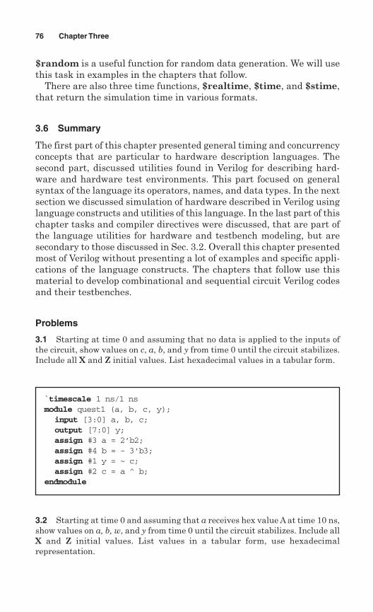
$random is a useful function for random data generation. We will usethis task in examples in the chapters that follow.
There are also three time functions, $realtime, $time, and $stime,that return the simulation time in various formats.
3.6 Summary
The first part of this chapter presented general timing and concurrencyconcepts that are particular to hardware description languages. Thesecond part, discussed utilities found in Verilog for describing hard-ware and hardware test environments. This part focused on generalsyntax of the language its operators, names, and data types. In the nextsection we discussed simulation of hardware described in Verilog usinglanguage constructs and utilities of this language. In the last part of thischapter tasks and compiler directives were discussed, that are part ofthe language utilities for hardware and testbench modeling, but aresecondary to those discussed in Sec. 3.2. Overall this chapter presentedmost of Verilog without presenting a lot of examples and specific appli-cations of the language constructs. The chapters that follow use thismaterial to develop combinational and sequential circuit Verilog codesand their testbenches.
Problems
3.1 Starting at time 0 and assuming that no data is applied to the inputs ofthe circuit, show values on c, a, b, and y from time 0 until the circuit stabilizes.Include all X and Z initial values. List hexadecimal values in a tabular form.
76 Chapter Three
`timescale 1 ns/1 nsmodule quest1 (a, b, c, y);
input [3:0] a, b, c;output [7:0] y;assign #3 a = 2’b2;assign #4 b = - 3’b3;assign #1 y = ~ c;assign #2 c = a ^ b;
endmodule
3.2 Starting at time 0 and assuming that a receives hex value A at time 10 ns,show values on a, b, w, and y from time 0 until the circuit stabilizes. Include allX and Z initial values. List values in a tabular form, use hexadecimalrepresentation.
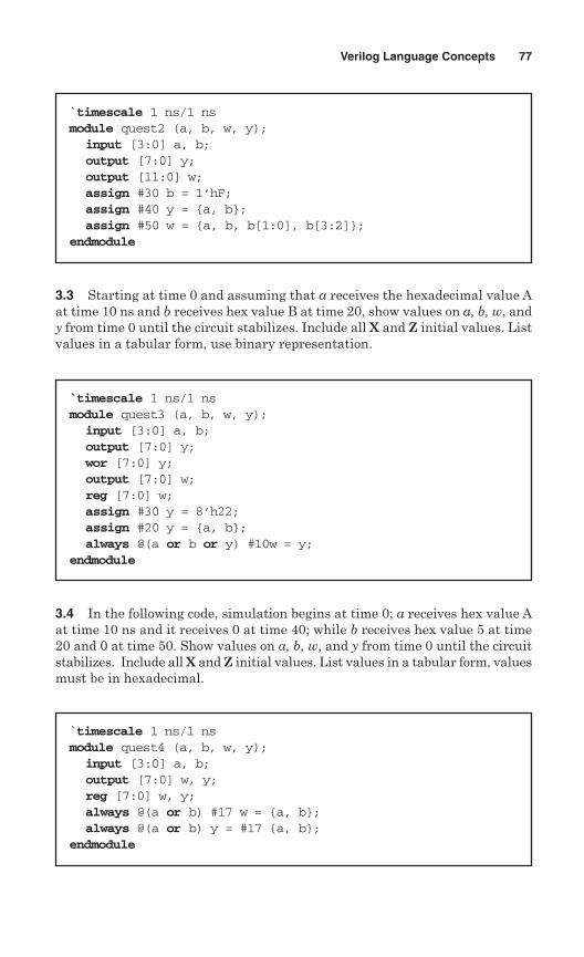
3.3 Starting at time 0 and assuming that a receives the hexadecimal value Aat time 10 ns and b receives hex value B at time 20, show values on a, b, w, andy from time 0 until the circuit stabilizes. Include all X and Z initial values. Listvalues in a tabular form, use binary representation.
Verilog Language Concepts 77
`timescale 1 ns/1 nsmodule quest2 (a, b, w, y);
input [3:0] a, b;output [7:0] y;output [11:0] w;assign #30 b = 1’hF;assign #40 y = {a, b};assign #50 w = {a, b, b[1:0], b[3:2]};
endmodule
`timescale 1 ns/1 nsmodule quest3 (a, b, w, y);
input [3:0] a, b;output [7:0] y; wor [7:0] y;output [7:0] w;reg [7:0] w;assign #30 y = 8’h22;assign #20 y = {a, b};always @(a or b or y) #10w = y;
endmodule
3.4 In the following code, simulation begins at time 0; a receives hex value Aat time 10 ns and it receives 0 at time 40; while b receives hex value 5 at time20 and 0 at time 50. Show values on a, b, w, and y from time 0 until the circuitstabilizes. Include all X and Z initial values. List values in a tabular form, valuesmust be in hexadecimal.
`timescale 1 ns/1 nsmodule quest4 (a, b, w, y);
input [3:0] a, b;output [7:0] w, y;reg [7:0] w, y;always @(a or b) #17 w = {a, b};always @(a or b) y = #17 {a, b};
endmodule
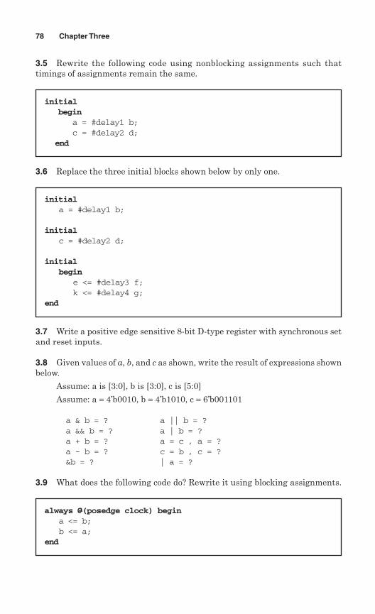
3.5 Rewrite the following code using nonblocking assignments such thattimings of assignments remain the same.
78 Chapter Three
initialbegin
a = #delay1 b;c = #delay2 d;
end
3.6 Replace the three initial blocks shown below by only one.
initiala = #delay1 b;
initialc = #delay2 d;
initialbegin
e <= #delay3 f;k <= #delay4 g;
end
3.7 Write a positive edge sensitive 8-bit D-type register with synchronous setand reset inputs.
3.8 Given values of a, b, and c as shown, write the result of expressions shownbelow.
Assume: a is [3:0], b is [3:0], c is [5:0]
Assume: a = 4’b0010, b = 4’b1010, c = 6’b001101
a & b = ? a || b = ?a && b = ? a | b = ?a + b = ? a = c , a = ?a - b = ? c = b , c = ?&b = ? | a = ?
3.9 What does the following code do? Rewrite it using blocking assignments.
always @(posedge clock) begina <= b;b <= a;
end
3.10 What does the following code do? Rewrite it using blocking assignments.
Verilog Language Concepts 79
always @(posedge clock)#0 a <= b + c;
always @(posedge clock)b <= a;
3.11 Show waveform on d for the entire simulation time.
3.12 Memory indexing. A) Declare a 4K memory with word size of 8, and a1-bit flag. B) Select the 5th bit of the 12th word of the memory and put it in theflag. All these operations must be done as continuous assign statements.
3.13 Show waveforms for a, b, and c for the first 100 ns of simulation.
`timescale 1ns/100psmodule test;reg b,c,d;
initial beginb=1’b1;c=1’b0;#10 b=1’b0;endinitial d = #25(b|c);
endmodule
Module test;wire a, b;reg c;assign #60 a = 1 ;initial begin
#20 c = b;#20 c = a;#20;
endendmodule
3.14 Show values of x, y, and z in the first 100 ns of simulation.
80 Chapter Three
module test;wire a;reg x, y, z;assign #25 a = 1 ;always begin
#20;x = #10 a;#3 y = a;#3 z = a;#7;
endendmodule
Suggested Reading
Brown, S., and Z. Vranesic, “Fundamentals of Digital Logic with Verilog Design”, McGraw-Hill; New York, 2002, ISBN: 0-07-283878-7.
Navabi, Z., “Verilog Computer-Based Training Course”; CBT CD with hardcopy User’smanual, McGraw-Hill, New York, 2002, ISBN 0-07-137473-6.
IEEE Std 1364-2001, IEEE Standard Verilog Language Reference Manual, SH94921-TBR (print) SS94921-TBR (electronic), ISBN 0-7381-2827-9 (print and electronic),2001.
IEEE Std 1076-2002, IEEE Standard VHDL Language Reference Manual, SH94983-TBR(print) SS94983-TBR (electronic), ISBN 0-7381-3247-0 (print) 0-7381-3248-9 (electronic),2002.
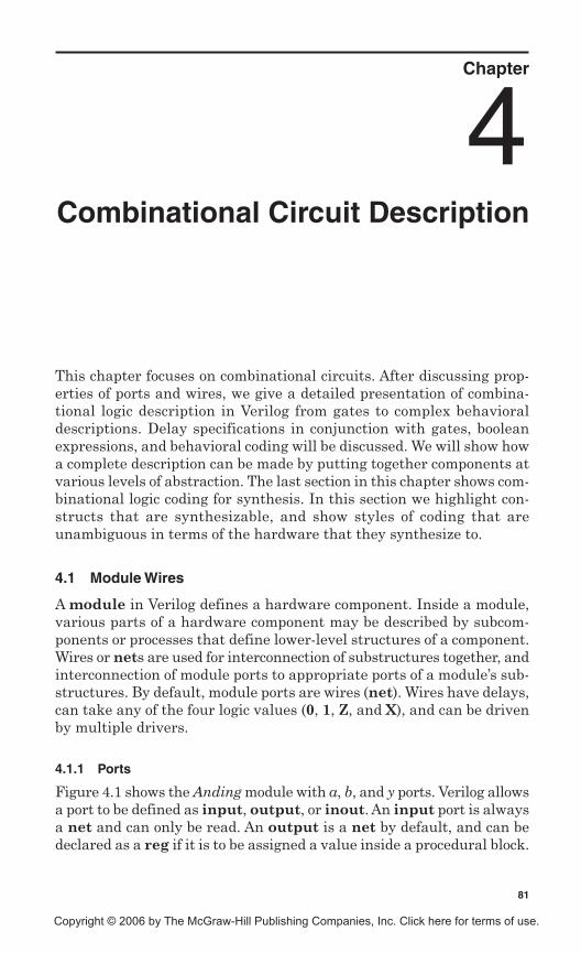
Chapter
4Combinational Circuit Description
This chapter focuses on combinational circuits. After discussing prop-erties of ports and wires, we give a detailed presentation of combina-tional logic description in Verilog from gates to complex behavioraldescriptions. Delay specifications in conjunction with gates, booleanexpressions, and behavioral coding will be discussed. We will show howa complete description can be made by putting together components atvarious levels of abstraction. The last section in this chapter shows com-binational logic coding for synthesis. In this section we highlight con-structs that are synthesizable, and show styles of coding that areunambiguous in terms of the hardware that they synthesize to.
4.1 Module Wires
A module in Verilog defines a hardware component. Inside a module,various parts of a hardware component may be described by subcom-ponents or processes that define lower-level structures of a component.Wires or nets are used for interconnection of substructures together, andinterconnection of module ports to appropriate ports of a module’s sub-structures. By default, module ports are wires (net). Wires have delays,can take any of the four logic values (0, 1, Z, and X), and can be drivenby multiple drivers.
4.1.1 Ports
Figure 4.1 shows the Anding module with a, b, and y ports. Verilog allowsa port to be defined as input, output, or inout. An input port is alwaysa net and can only be read. An output is a net by default, and can bedeclared as a reg if it is to be assigned a value inside a procedural block.
81
Copyright © 2006 by The McGraw-Hill Publishing Companies, Inc. Click here for terms of use.
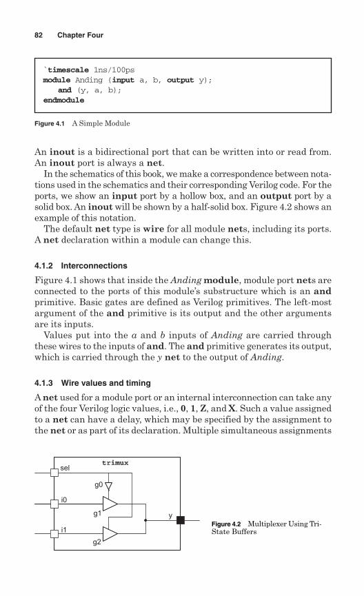
An inout is a bidirectional port that can be written into or read from.An inout port is always a net.
In the schematics of this book, we make a correspondence between nota-tions used in the schematics and their corresponding Verilog code. For theports, we show an input port by a hollow box, and an output port by asolid box. An inout will be shown by a half-solid box. Figure 4.2 shows anexample of this notation.
The default net type is wire for all module nets, including its ports.A net declaration within a module can change this.
4.1.2 Interconnections
Figure 4.1 shows that inside the Anding module, module port nets areconnected to the ports of this module’s substructure which is an andprimitive. Basic gates are defined as Verilog primitives. The left-mostargument of the and primitive is its output and the other argumentsare its inputs.
Values put into the a and b inputs of Anding are carried throughthese wires to the inputs of and. The and primitive generates its output,which is carried through the y net to the output of Anding.
4.1.3 Wire values and timing
A net used for a module port or an internal interconnection can take anyof the four Verilog logic values, i.e., 0, 1, Z, and X. Such a value assignedto a net can have a delay, which may be specified by the assignment tothe net or as part of its declaration. Multiple simultaneous assignments
82 Chapter Four
Figure 4.1 A Simple Module
`timescale 1ns/100psmodule Anding (input a, b, output y);
and (y, a, b);endmodule
trimuxsel
i0
i1
g0
g1
g2
yFigure 4.2 Multiplexer Using Tri-State Buffers
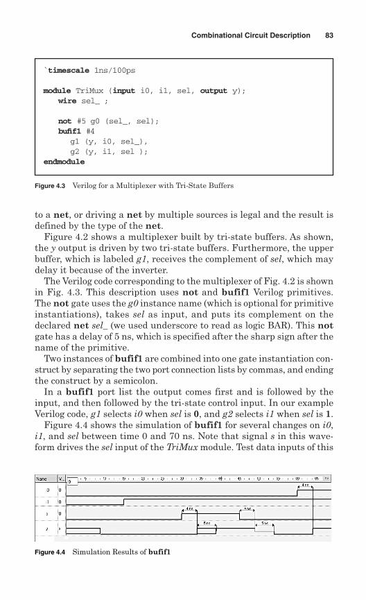
to a net, or driving a net by multiple sources is legal and the result isdefined by the type of the net.
Figure 4.2 shows a multiplexer built by tri-state buffers. As shown,the y output is driven by two tri-state buffers. Furthermore, the upperbuffer, which is labeled g1, receives the complement of sel, which maydelay it because of the inverter.
The Verilog code corresponding to the multiplexer of Fig. 4.2 is shownin Fig. 4.3. This description uses not and bufif1 Verilog primitives.The not gate uses the g0 instance name (which is optional for primitiveinstantiations), takes sel as input, and puts its complement on thedeclared net sel_ (we used underscore to read as logic BAR). This notgate has a delay of 5 ns, which is specified after the sharp sign after thename of the primitive.
Two instances of bufif1 are combined into one gate instantiation con-struct by separating the two port connection lists by commas, and endingthe construct by a semicolon.
In a bufif1 port list the output comes first and is followed by theinput, and then followed by the tri-state control input. In our exampleVerilog code, g1 selects i0 when sel is 0, and g2 selects i1 when sel is 1.
Figure 4.4 shows the simulation of bufif1 for several changes on i0,i1, and sel between time 0 and 70 ns. Note that signal s in this wave-form drives the sel input of the TriMux module. Test data inputs of this
Combinational Circuit Description 83
Figure 4.3 Verilog for a Multiplexer with Tri-State Buffers
`timescale 1ns/100ps
module TriMux (input i0, i1, sel, output y);wire sel_ ;
not #5 g0 (sel_, sel);bufif1 #4
g1 (y, i0, sel_),g2 (y, i1, sel );
endmodule
Figure 4.4 Simulation Results of bufif1
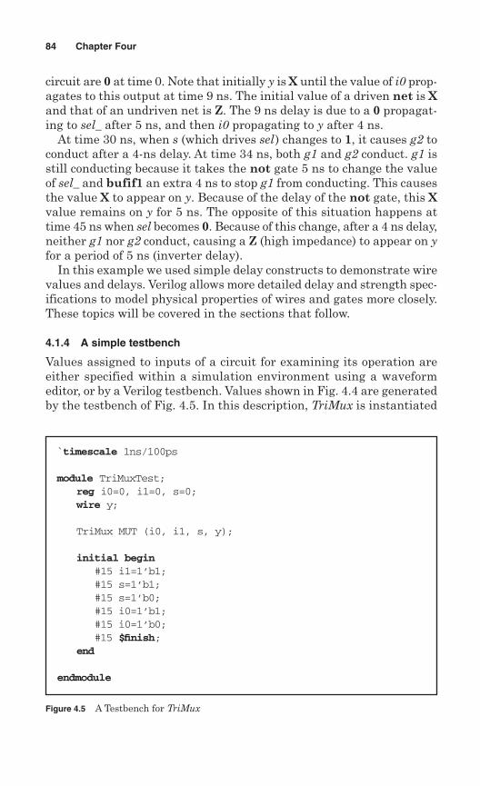
circuit are 0 at time 0. Note that initially y is X until the value of i0 prop-agates to this output at time 9 ns. The initial value of a driven net is Xand that of an undriven net is Z. The 9 ns delay is due to a 0 propagat-ing to sel_ after 5 ns, and then i0 propagating to y after 4 ns.
At time 30 ns, when s (which drives sel) changes to 1, it causes g2 toconduct after a 4-ns delay. At time 34 ns, both g1 and g2 conduct. g1 isstill conducting because it takes the not gate 5 ns to change the valueof sel_ and bufif1 an extra 4 ns to stop g1 from conducting. This causesthe value X to appear on y. Because of the delay of the not gate, this Xvalue remains on y for 5 ns. The opposite of this situation happens attime 45 ns when sel becomes 0. Because of this change, after a 4 ns delay,neither g1 nor g2 conduct, causing a Z (high impedance) to appear on yfor a period of 5 ns (inverter delay).
In this example we used simple delay constructs to demonstrate wirevalues and delays. Verilog allows more detailed delay and strength spec-ifications to model physical properties of wires and gates more closely.These topics will be covered in the sections that follow.
4.1.4 A simple testbench
Values assigned to inputs of a circuit for examining its operation areeither specified within a simulation environment using a waveformeditor, or by a Verilog testbench. Values shown in Fig. 4.4 are generatedby the testbench of Fig. 4.5. In this description, TriMux is instantiated
84 Chapter Four
Figure 4.5 A Testbench for TriMux
`timescale 1ns/100ps
module TriMuxTest;reg i0=0, i1=0, s=0;wire y;
TriMux MUT (i0, i1, s, y);
initial begin#15 i1=1’b1;#15 s=1’b1;#15 s=1’b0;#15 i0=1’b1;#15 i0=1’b0;#15 $finish;
end
endmodule
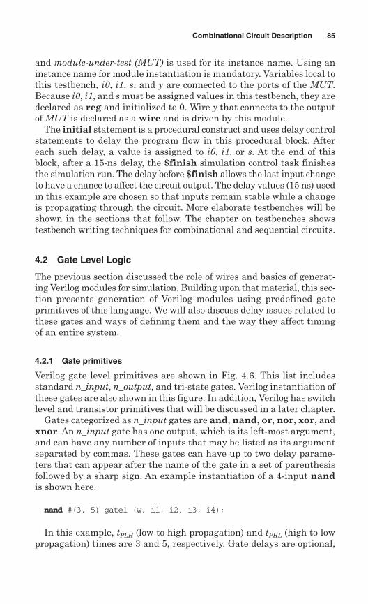
and module-under-test (MUT) is used for its instance name. Using aninstance name for module instantiation is mandatory. Variables local tothis testbench, i0, i1, s, and y are connected to the ports of the MUT.Because i0, i1, and s must be assigned values in this testbench, they aredeclared as reg and initialized to 0. Wire y that connects to the outputof MUT is declared as a wire and is driven by this module.
The initial statement is a procedural construct and uses delay controlstatements to delay the program flow in this procedural block. Aftereach such delay, a value is assigned to i0, i1, or s. At the end of thisblock, after a 15-ns delay, the $finish simulation control task finishesthe simulation run. The delay before $finish allows the last input changeto have a chance to affect the circuit output. The delay values (15 ns) usedin this example are chosen so that inputs remain stable while a changeis propagating through the circuit. More elaborate testbenches will beshown in the sections that follow. The chapter on testbenches showstestbench writing techniques for combinational and sequential circuits.
4.2 Gate Level Logic
The previous section discussed the role of wires and basics of generat-ing Verilog modules for simulation. Building upon that material, this sec-tion presents generation of Verilog modules using predefined gateprimitives of this language. We will also discuss delay issues related tothese gates and ways of defining them and the way they affect timingof an entire system.
4.2.1 Gate primitives
Verilog gate level primitives are shown in Fig. 4.6. This list includesstandard n_input, n_output, and tri-state gates. Verilog instantiation ofthese gates are also shown in this figure. In addition, Verilog has switchlevel and transistor primitives that will be discussed in a later chapter.
Gates categorized as n_input gates are and, nand, or, nor, xor, andxnor. An n_input gate has one output, which is its left-most argument,and can have any number of inputs that may be listed as its argumentseparated by commas. These gates can have up to two delay parame-ters that can appear after the name of the gate in a set of parenthesisfollowed by a sharp sign. An example instantiation of a 4-input nandis shown here.
nand #(3, 5) gate1 (w, i1, i2, i3, i4);
In this example, tPLH (low to high propagation) and tPHL (high to lowpropagation) times are 3 and 5, respectively. Gate delays are optional,
Combinational Circuit Description 85
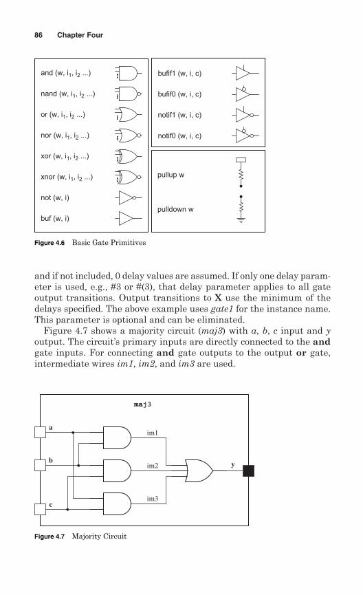
and if not included, 0 delay values are assumed. If only one delay param-eter is used, e.g., #3 or #(3), that delay parameter applies to all gateoutput transitions. Output transitions to X use the minimum of thedelays specified. The above example uses gate1 for the instance name.This parameter is optional and can be eliminated.
Figure 4.7 shows a majority circuit (maj3) with a, b, c input and youtput. The circuit’s primary inputs are directly connected to the andgate inputs. For connecting and gate outputs to the output or gate,intermediate wires im1, im2, and im3 are used.
86 Chapter Four
and (w, i1, i2 ...)
nand (w, i1, i2 ...)
or (w, i1, i2 ...)
nor (w, i1, i2 ...)
xor (w, i1, i2 ...)
xnor (w, i1, i2 ...)
not (w, i)
buf (w, i)
bufif1 (w, i, c)
bufif0 (w, i, c)
notif1 (w, i, c)
notif0 (w, i, c)
pullup w
pulldown w
Figure 4.6 Basic Gate Primitives
im1
im2
im3
a
maj3
b
c
y
Figure 4.7 Majority Circuit
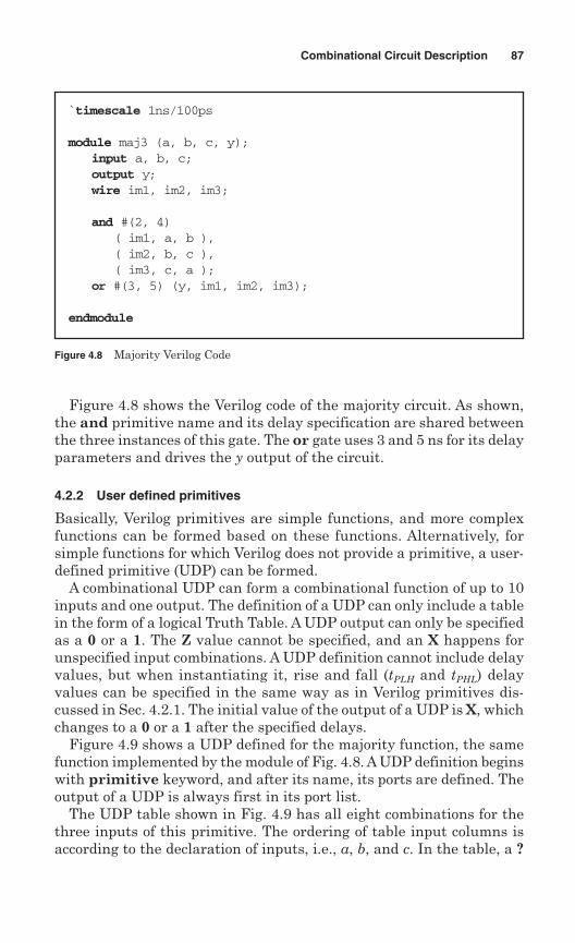
Figure 4.8 shows the Verilog code of the majority circuit. As shown,the and primitive name and its delay specification are shared betweenthe three instances of this gate. The or gate uses 3 and 5 ns for its delayparameters and drives the y output of the circuit.
4.2.2 User defined primitives
Basically, Verilog primitives are simple functions, and more complexfunctions can be formed based on these functions. Alternatively, forsimple functions for which Verilog does not provide a primitive, a user-defined primitive (UDP) can be formed.
A combinational UDP can form a combinational function of up to 10inputs and one output. The definition of a UDP can only include a tablein the form of a logical Truth Table. A UDP output can only be specifiedas a 0 or a 1. The Z value cannot be specified, and an X happens forunspecified input combinations. A UDP definition cannot include delayvalues, but when instantiating it, rise and fall (tPLH and tPHL) delayvalues can be specified in the same way as in Verilog primitives dis-cussed in Sec. 4.2.1. The initial value of the output of a UDP is X, whichchanges to a 0 or a 1 after the specified delays.
Figure 4.9 shows a UDP defined for the majority function, the samefunction implemented by the module of Fig. 4.8. A UDP definition beginswith primitive keyword, and after its name, its ports are defined. Theoutput of a UDP is always first in its port list.
The UDP table shown in Fig. 4.9 has all eight combinations for thethree inputs of this primitive. The ordering of table input columns isaccording to the declaration of inputs, i.e., a, b, and c. In the table, a ?
Combinational Circuit Description 87
Figure 4.8 Majority Verilog Code
`timescale 1ns/100ps
module maj3 (a, b, c, y);input a, b, c;output y;wire im1, im2, im3;
and #(2, 4) ( im1, a, b ),( im2, b, c ),( im3, c, a );
or #(3, 5) (y, im1, im2, im3);
endmodule
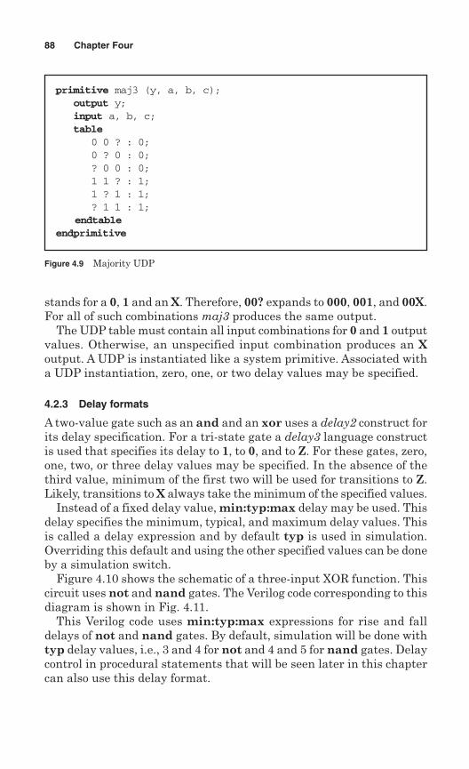
stands for a 0, 1 and an X. Therefore, 00? expands to 000, 001, and 00X.For all of such combinations maj3 produces the same output.
The UDP table must contain all input combinations for 0 and 1 outputvalues. Otherwise, an unspecified input combination produces an Xoutput. A UDP is instantiated like a system primitive. Associated witha UDP instantiation, zero, one, or two delay values may be specified.
4.2.3 Delay formats
A two-value gate such as an and and an xor uses a delay2 construct forits delay specification. For a tri-state gate a delay3 language constructis used that specifies its delay to 1, to 0, and to Z. For these gates, zero,one, two, or three delay values may be specified. In the absence of thethird value, minimum of the first two will be used for transitions to Z.Likely, transitions to X always take the minimum of the specified values.
Instead of a fixed delay value, min:typ:max delay may be used. Thisdelay specifies the minimum, typical, and maximum delay values. Thisis called a delay expression and by default typ is used in simulation.Overriding this default and using the other specified values can be doneby a simulation switch.
Figure 4.10 shows the schematic of a three-input XOR function. Thiscircuit uses not and nand gates. The Verilog code corresponding to thisdiagram is shown in Fig. 4.11.
This Verilog code uses min:typ:max expressions for rise and falldelays of not and nand gates. By default, simulation will be done withtyp delay values, i.e., 3 and 4 for not and 4 and 5 for nand gates. Delaycontrol in procedural statements that will be seen later in this chaptercan also use this delay format.
88 Chapter Four
Figure 4.9 Majority UDP
primitive maj3 (y, a, b, c);output y;input a, b, c;table
0 0 ? : 0;0 ? 0 : 0;? 0 0 : 0;1 1 ? : 1;1 ? 1 : 1;? 1 1 : 1;
endtableendprimitive
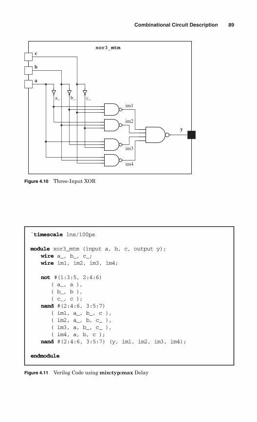
Combinational Circuit Description 89
im1
im2
im3
a
im4
b
c
c_b_a_
y
xor3_mtm
Figure 4.10 Three-Input XOR
Figure 4.11 Verilog Code using min:typ:max Delay
`timescale 1ns/100ps
module xor3_mtm (input a, b, c, output y);wire a_, b_, c_;wire im1, im2, im3, im4;
not #(1:3:5, 2:4:6) ( a_, a ),( b_, b ),( c_, c );
nand #(2:4:6, 3:5:7) ( im1, a_, b_, c ),( im2, a_, b, c_ ),( im3, a, b_, c_ ),( im4, a, b, c );
nand #(2:4:6, 3:5:7) (y, im1, im2, im3, im4);
endmodule
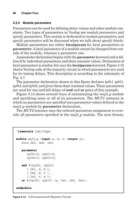
4.2.4 Module parameters
Parameters can be used for defining delay values and other module con-stants. Two types of parameters in Verilog are module parameters andspecify parameters. This section is dedicated to module parameters, andspecify parameters will be discussed when we talk about specify blocks.
Module parameters are either localparam for local parameters orparameter. A local parameter of a module cannot be changed from out-side of the module, whereas a parameter can.
Aparameter declaration begins with the parameter keyword and is fol-lowed by individual parameters and their constant values. Declaration oflocal parameters is similar, but uses the localparam keyword. Figure 4.12shows Verilog code of the majority circuit in which parameters are usedfor its timing delays. This description is according to the schematic ofFig. 4.7.
The parameter declaration shown in this figure declares tplh1, tphl1,tplh2, and tphl2, and gives them their constant values. These parametersare used for rise and fall delays of and and or gates of this example.
Figure 4.13 shows several ways of instantiating the maj3_p moduleand specifying some or all of its parameters. The MUT1 instance inwhich no parameters are specified uses parameter values defined in themaj3_p module by parameter declaration.
The MUT2 instance uses the ordered parameter assignment to over-ride all parameters specified in the maj3_p module. The next format,
90 Chapter Four
Figure 4.12 A Parameterized Majority Circuit
`timescale 1ns/100ps
module maj3_p (input a, b, c, output y);wire im1, im2, im3;
parametertplh1=2, tphl1=4,tplh2=3, tphl2=5;
and #(tplh1, tphl1) ( im1, a, b ),( im2, b, c ),( im3, c, a );
or #(tplh2, tphl2) (y, im1, im2, im3);
endmodule
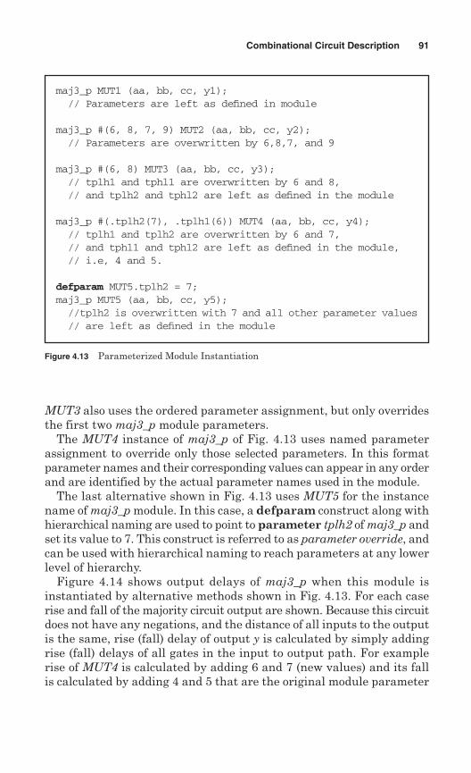
MUT3 also uses the ordered parameter assignment, but only overridesthe first two maj3_p module parameters.
The MUT4 instance of maj3_p of Fig. 4.13 uses named parameterassignment to override only those selected parameters. In this formatparameter names and their corresponding values can appear in any orderand are identified by the actual parameter names used in the module.
The last alternative shown in Fig. 4.13 uses MUT5 for the instancename of maj3_p module. In this case, a defparam construct along withhierarchical naming are used to point to parameter tplh2 of maj3_p andset its value to 7. This construct is referred to as parameter override, andcan be used with hierarchical naming to reach parameters at any lowerlevel of hierarchy.
Figure 4.14 shows output delays of maj3_p when this module isinstantiated by alternative methods shown in Fig. 4.13. For each caserise and fall of the majority circuit output are shown. Because this circuitdoes not have any negations, and the distance of all inputs to the outputis the same, rise (fall) delay of output y is calculated by simply addingrise (fall) delays of all gates in the input to output path. For examplerise of MUT4 is calculated by adding 6 and 7 (new values) and its fallis calculated by adding 4 and 5 that are the original module parameter
Combinational Circuit Description 91
Figure 4.13 Parameterized Module Instantiation
maj3_p MUT1 (aa, bb, cc, y1); // Parameters are left as defined in module
maj3_p #(6, 8, 7, 9) MUT2 (aa, bb, cc, y2);// Parameters are overwritten by 6,8,7, and 9
maj3_p #(6, 8) MUT3 (aa, bb, cc, y3);// tplh1 and tphl1 are overwritten by 6 and 8,// and tplh2 and tphl2 are left as defined in the module
maj3_p #(.tplh2(7), .tplh1(6)) MUT4 (aa, bb, cc, y4);// tplh1 and tplh2 are overwritten by 6 and 7,// and tphl1 and tphl2 are left as defined in the module, // i.e, 4 and 5.
defparam MUT5.tplh2 = 7;maj3_p MUT5 (aa, bb, cc, y5);//tplh2 is overwritten with 7 and all other parameter values// are left as defined in the module
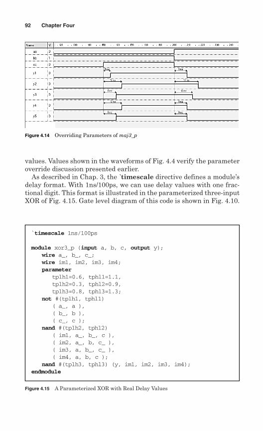
values. Values shown in the waveforms of Fig. 4.4 verify the parameteroverride discussion presented earlier.
As described in Chap. 3, the `timescale directive defines a module’sdelay format. With 1ns/100ps, we can use delay values with one frac-tional digit. This format is illustrated in the parameterized three-inputXOR of Fig. 4.15. Gate level diagram of this code is shown in Fig. 4.10.
92 Chapter Four
Figure 4.15 A Parameterized XOR with Real Delay Values
`timescale 1ns/100ps
module xor3_p (input a, b, c, output y);wire a_, b_, c_;wire im1, im2, im3, im4;parameter
tplh1=0.6, tphl1=1.1,tplh2=0.3, tphl2=0.9,tplh3=0.8, tphl3=1.3;
not #(tplh1, tphl1) ( a_, a ),( b_, b ),( c_, c );
nand #(tplh2, tphl2) ( im1, a_, b_, c ),( im2, a_, b, c_ ),( im3, a, b_, c_ ),( im4, a, b, c );
nand #(tplh3, tphl3) (y, im1, im2, im3, im4); endmodule
Figure 4.14 Overriding Parameters of maj3_p
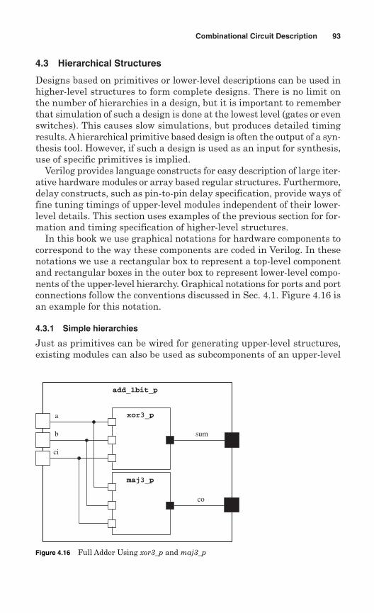
4.3 Hierarchical Structures
Designs based on primitives or lower-level descriptions can be used inhigher-level structures to form complete designs. There is no limit onthe number of hierarchies in a design, but it is important to rememberthat simulation of such a design is done at the lowest level (gates or evenswitches). This causes slow simulations, but produces detailed timingresults. A hierarchical primitive based design is often the output of a syn-thesis tool. However, if such a design is used as an input for synthesis,use of specific primitives is implied.
Verilog provides language constructs for easy description of large iter-ative hardware modules or array based regular structures. Furthermore,delay constructs, such as pin-to-pin delay specification, provide ways offine tuning timings of upper-level modules independent of their lower-level details. This section uses examples of the previous section for for-mation and timing specification of higher-level structures.
In this book we use graphical notations for hardware components tocorrespond to the way these components are coded in Verilog. In thesenotations we use a rectangular box to represent a top-level componentand rectangular boxes in the outer box to represent lower-level compo-nents of the upper-level hierarchy. Graphical notations for ports and portconnections follow the conventions discussed in Sec. 4.1. Figure 4.16 isan example for this notation.
4.3.1 Simple hierarchies
Just as primitives can be wired for generating upper-level structures,existing modules can also be used as subcomponents of an upper-level
Combinational Circuit Description 93
xor3_p
maj3_p
a
b
ci
sum
co
add_1bit_p
Figure 4.16 Full Adder Using xor3_p and maj3_p
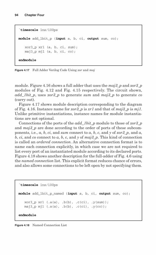
module. Figure 4.16 shows a full adder that uses the maj3_p and xor3_pmodules of Fig. 4.12 and Fig. 4.15 respectively. The circuit shown,add_1bit_p, uses xor3_p to generate sum and maj3_p to generate co(carry out).
Figure 4.17 shows module description corresponding to the diagramof Fig. 4.16. Instance name for xor3_p is xr1 and that of maj3_p is mj1.Unlike primitive instantiations, instance names for module instantia-tions are not optional.
Connections of the ports of the add_1bit_p module to those of xor3_pand maj3_p are done according to the order of ports of these subcom-ponents, i.e., a, b, ci, and sum connect to a, b, c, and y of xor3_p, and a,b, ci, and co connect to a, b, c, and y of maj3_p. This kind of connectionis called an ordered connection. An alternative connection format is toname each connection explicitly, in which case we are not required tolist every port of an instantiated module according to its declared ports.Figure 4.18 shows another description for the full-adder of Fig. 4.6 usingthe named connection list. This explicit format reduces chance of errors,and also allows some connections to be left open by not specifying them.
94 Chapter Four
Figure 4.17 Full Adder Verilog Code Using xor and maj
`timescale 1ns/100ps
module add_1bit_p (input a, b, ci, output sum, co);
xor3_p xr1 (a, b, ci, sum);maj3_p mj1 (a, b, ci, co);
endmodule
Figure 4.18 Named Connection List
`timescale 1ns/100ps
module add_1bit_p_named (input a, b, ci, output sum, co);
xor3_p xr1 (.a(a), .b(b), .c(ci), .y(sum));maj3_p mj1 (.a(a), .b(b), .c(ci), .y(co));
endmodule
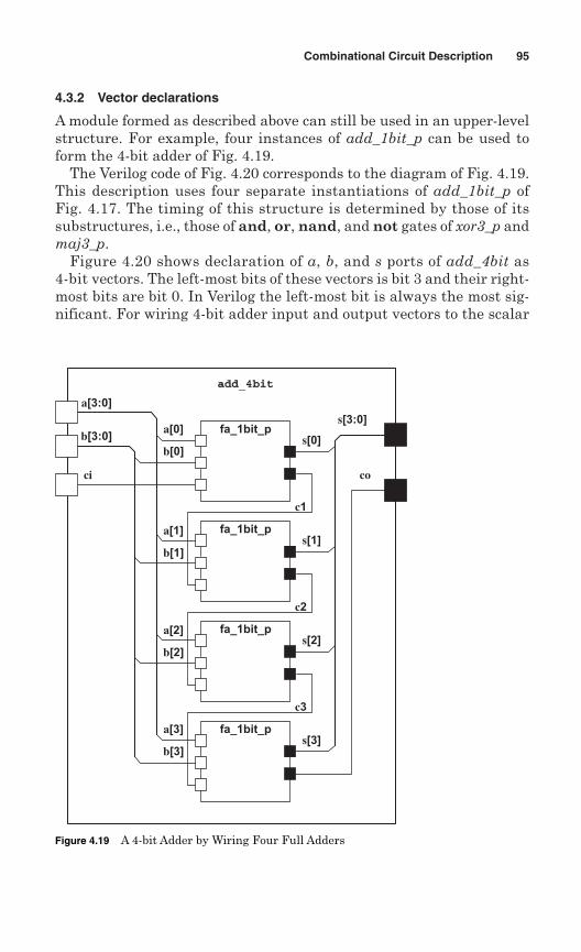
4.3.2 Vector declarations
A module formed as described above can still be used in an upper-levelstructure. For example, four instances of add_1bit_p can be used toform the 4-bit adder of Fig. 4.19.
The Verilog code of Fig. 4.20 corresponds to the diagram of Fig. 4.19.This description uses four separate instantiations of add_1bit_p ofFig. 4.17. The timing of this structure is determined by those of itssubstructures, i.e., those of and, or, nand, and not gates of xor3_p andmaj3_p.
Figure 4.20 shows declaration of a, b, and s ports of add_4bit as4-bit vectors. The left-most bits of these vectors is bit 3 and their right-most bits are bit 0. In Verilog the left-most bit is always the most sig-nificant. For wiring 4-bit adder input and output vectors to the scalar
Combinational Circuit Description 95
fa_1bit_p
a[3:0]
b[3:0]
ci
s[3:0]
co
add_4bit
c1
c2
c3
a[0]
b[0]
a[1]
b[1]
a[2]
b[2]
a[3]
b[3]s[3]
s[2]
s[1]
s[0]
fa_1bit_p
fa_1bit_p
fa_1bit_p
Figure 4.19 A 4-bit Adder by Wiring Four Full Adders
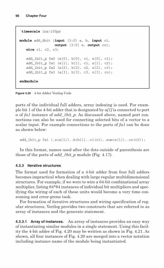
ports of the individual full adders, array indexing is used. For exam-ple bit 1 of the 4-bit adder that is designated by a[1] is connected to porta of fa1 instance of add_1bit_p. As discussed above, named port con-nections can also be used for connecting selected bits of a vector to ascalar input. For example connections to the ports of fa1 can be doneas shown below:
add_1bit_p fa1 (.a(a[1]),.b(b[1],.ci(c1),.sum(s[1]),.co(c2));
In this format, names used after the dots outside of parenthesis arethose of the ports of add_1bit_p module (Fig. 4.17).
4.3.3 Iterative structures
The format used for formation of a 4-bit adder from four full addersbecomes impractical when dealing with large regular multidimensionalstructures. For example, if we were to wire a 64-bit combinational arraymultiplier, listing 64*64 instances of individual bit multipliers and spec-ifying the wiring of each of these units would become a very time con-suming and error-prone task.
For formation of iterative structures and wiring specification of reg-ular structures, Verilog provides two constructs that are referred to asarray of instances and the generate statement.
4.3.3.1 Array of instances. An array of instances provides an easy wayof instantiating similar modules in a single statement. Using this facil-ity the 4-bit adder of Fig. 4.20 may be written as shown in Fig. 4.21. Asshown, all four instances of Fig. 4.20 are merged into a vector notationincluding instance name of the module being instantiated.
96 Chapter Four
Figure 4.20 4-bit Adder Verilog Code
`timescale 1ns/100ps
module add_4bit (input [3:0] a, b, input ci,output [3:0] s, output co);
wire c1, c2, c3;
add_1bit_p fa0 (a[0], b[0], ci, s[0], c1);add_1bit_p fa1 (a[1], b[1], c1, s[1], c2);add_1bit_p fa2 (a[2], b[2], c2, s[2], c3);add_1bit_p fa3 (a[3], b[3], c3, s[3], co);
endmodule
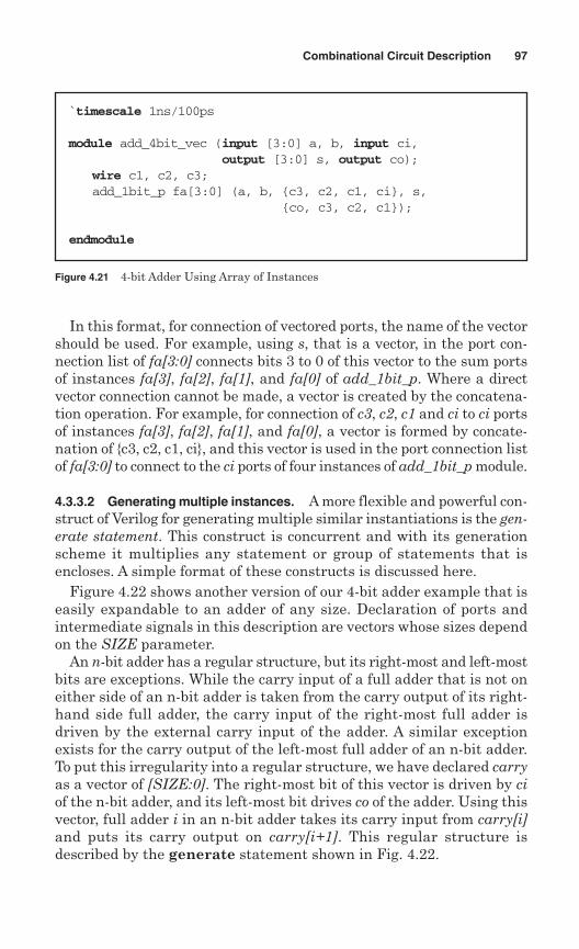
In this format, for connection of vectored ports, the name of the vectorshould be used. For example, using s, that is a vector, in the port con-nection list of fa[3:0] connects bits 3 to 0 of this vector to the sum portsof instances fa[3], fa[2], fa[1], and fa[0] of add_1bit_p. Where a directvector connection cannot be made, a vector is created by the concatena-tion operation. For example, for connection of c3, c2, c1 and ci to ci portsof instances fa[3], fa[2], fa[1], and fa[0], a vector is formed by concate-nation of {c3, c2, c1, ci}, and this vector is used in the port connection listof fa[3:0] to connect to the ci ports of four instances of add_1bit_p module.
4.3.3.2 Generating multiple instances. A more flexible and powerful con-struct of Verilog for generating multiple similar instantiations is the gen-erate statement. This construct is concurrent and with its generationscheme it multiplies any statement or group of statements that isencloses. A simple format of these constructs is discussed here.
Figure 4.22 shows another version of our 4-bit adder example that iseasily expandable to an adder of any size. Declaration of ports andintermediate signals in this description are vectors whose sizes dependon the SIZE parameter.
An n-bit adder has a regular structure, but its right-most and left-mostbits are exceptions. While the carry input of a full adder that is not oneither side of an n-bit adder is taken from the carry output of its right-hand side full adder, the carry input of the right-most full adder isdriven by the external carry input of the adder. A similar exceptionexists for the carry output of the left-most full adder of an n-bit adder.To put this irregularity into a regular structure, we have declared carryas a vector of [SIZE:0]. The right-most bit of this vector is driven by ciof the n-bit adder, and its left-most bit drives co of the adder. Using thisvector, full adder i in an n-bit adder takes its carry input from carry[i]and puts its carry output on carry[i+1]. This regular structure isdescribed by the generate statement shown in Fig. 4.22.
Combinational Circuit Description 97
Figure 4.21 4-bit Adder Using Array of Instances
`timescale 1ns/100ps
module add_4bit_vec (input [3:0] a, b, input ci,output [3:0] s, output co);
wire c1, c2, c3;add_1bit_p fa[3:0] (a, b, {c3, c2, c1, ci}, s,
{co, c3, c2, c1});
endmodule
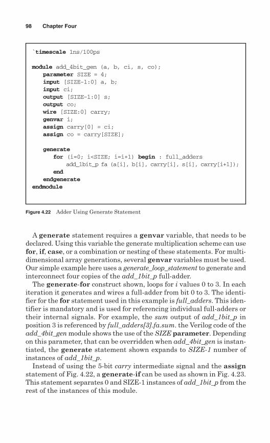
A generate statement requires a genvar variable, that needs to bedeclared. Using this variable the generate multiplication scheme can usefor, if, case, or a combination or nesting of these statements. For multi-dimensional array generations, several genvar variables must be used.Our simple example here uses a generate_loop_statement to generate andinterconnect four copies of the add_1bit_p full-adder.
The generate-for construct shown, loops for i values 0 to 3. In eachiteration it generates and wires a full-adder from bit 0 to 3. The identi-fier for the for statement used in this example is full_adders. This iden-tifier is mandatory and is used for referencing individual full-adders ortheir internal signals. For example, the sum output of add_1bit_p inposition 3 is referenced by full_adders[3].fa.sum. the Verilog code of theadd_4bit_gen module shows the use of the SIZE parameter. Dependingon this parameter, that can be overridden when add_4bit_gen is instan-tiated, the generate statement shown expands to SIZE-1 number ofinstances of add_1bit_p.
Instead of using the 5-bit carry intermediate signal and the assignstatement of Fig. 4.22, a generate-if can be used as shown in Fig. 4.23.This statement separates 0 and SIZE-1 instances of add_1bit_p from therest of the instances of this module.
98 Chapter Four
Figure 4.22 Adder Using Generate Statement
`timescale 1ns/100ps
module add_4bit_gen (a, b, ci, s, co);parameter SIZE = 4;input [SIZE-1:0] a, b;input ci;output [SIZE-1:0] s;output co;wire [SIZE:0] carry;genvar i;assign carry[0] = ci;assign co = carry[SIZE];
generatefor (i=0; i<SIZE; i=i+1) begin : full_adders
add_1bit_p fa (a[i], b[i], carry[i], s[i], carry[i+1]);end
endgenerateendmodule
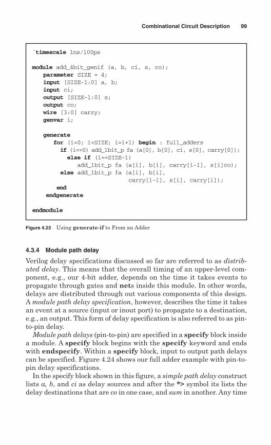
4.3.4 Module path delay
Verilog delay specifications discussed so far are referred to as distrib-uted delay. This means that the overall timing of an upper-level com-ponent, e.g., our 4-bit adder, depends on the time it takes events topropagate through gates and nets inside this module. In other words,delays are distributed through out various components of this design.A module path delay specification, however, describes the time it takesan event at a source (input or inout port) to propagate to a destination,e.g., an output. This form of delay specification is also referred to as pin-to-pin delay.
Module path delays (pin-to-pin) are specified in a specify block insidea module. A specify block begins with the specify keyword and endswith endspecify. Within a specify block, input to output path delayscan be specified. Figure 4.24 shows our full adder example with pin-to-pin delay specifications.
In the specify block shown in this figure, a simple path delay constructlists a, b, and ci as delay sources and after the *> symbol its lists thedelay destinations that are co in one case, and sum in another. Any time
Combinational Circuit Description 99
Figure 4.23 Using generate-if to From an Adder
`timescale 1ns/100ps
module add_4bit_genif (a, b, ci, s, co);parameter SIZE = 4;input [SIZE-1:0] a, b;input ci;output [SIZE-1:0] s;output co;wire [3:0] carry;genvar i;
generatefor (i=0; i<SIZE; i=i+1) begin : full_addersif (i==0) add_1bit_p fa (a[0], b[0], ci, s[0], carry[0]);else if (i==SIZE-1)
add_1bit_p fa (a[i], b[i], carry[i-1], s[i]co);else add_1bit_p fa (a[i], b[i],
carry[i-1], s[i], carry[i]);end
endgenerate
endmodule
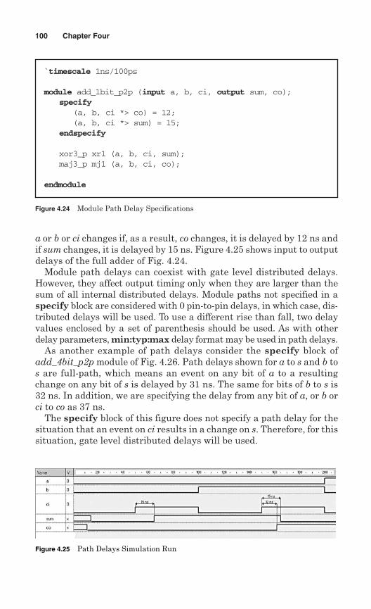
a or b or ci changes if, as a result, co changes, it is delayed by 12 ns andif sum changes, it is delayed by 15 ns. Figure 4.25 shows input to outputdelays of the full adder of Fig. 4.24.
Module path delays can coexist with gate level distributed delays.However, they affect output timing only when they are larger than thesum of all internal distributed delays. Module paths not specified in aspecify block are considered with 0 pin-to-pin delays, in which case, dis-tributed delays will be used. To use a different rise than fall, two delayvalues enclosed by a set of parenthesis should be used. As with otherdelay parameters, min:typ:max delay format may be used in path delays.
As another example of path delays consider the specify block ofadd_4bit_p2p module of Fig. 4.26. Path delays shown for a to s and b tos are full-path, which means an event on any bit of a to a resultingchange on any bit of s is delayed by 31 ns. The same for bits of b to s is32 ns. In addition, we are specifying the delay from any bit of a, or b orci to co as 37 ns.
The specify block of this figure does not specify a path delay for thesituation that an event on ci results in a change on s. Therefore, for thissituation, gate level distributed delays will be used.
100 Chapter Four
Figure 4.24 Module Path Delay Specifications
`timescale 1ns/100ps
module add_1bit_p2p (input a, b, ci, output sum, co);specify
(a, b, ci *> co) = 12;(a, b, ci *> sum) = 15;
endspecify
xor3_p xr1 (a, b, ci, sum);maj3_p mj1 (a, b, ci, co);
endmodule
Figure 4.25 Path Delays Simulation Run
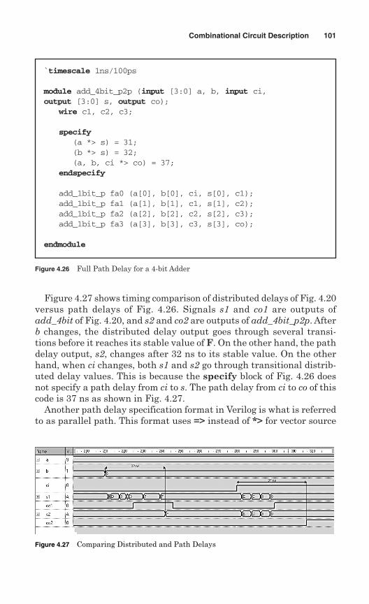
Figure 4.27 shows timing comparison of distributed delays of Fig. 4.20versus path delays of Fig. 4.26. Signals s1 and co1 are outputs ofadd_4bit of Fig. 4.20, and s2 and co2 are outputs of add_4bit_p2p. Afterb changes, the distributed delay output goes through several transi-tions before it reaches its stable value of F. On the other hand, the pathdelay output, s2, changes after 32 ns to its stable value. On the otherhand, when ci changes, both s1 and s2 go through transitional distrib-uted delay values. This is because the specify block of Fig. 4.26 doesnot specify a path delay from ci to s. The path delay from ci to co of thiscode is 37 ns as shown in Fig. 4.27.
Another path delay specification format in Verilog is what is referredto as parallel path. This format uses => instead of *> for vector source
Combinational Circuit Description 101
Figure 4.26 Full Path Delay for a 4-bit Adder
`timescale 1ns/100ps
module add_4bit_p2p (input [3:0] a, b, input ci,output [3:0] s, output co);
wire c1, c2, c3;
specify(a *> s) = 31;(b *> s) = 32;(a, b, ci *> co) = 37;
endspecify
add_1bit_p fa0 (a[0], b[0], ci, s[0], c1);add_1bit_p fa1 (a[1], b[1], c1, s[1], c2);add_1bit_p fa2 (a[2], b[2], c2, s[2], c3);add_1bit_p fa3 (a[3], b[3], c3, s[3], co);
endmodule
Figure 4.27 Comparing Distributed and Path Delays
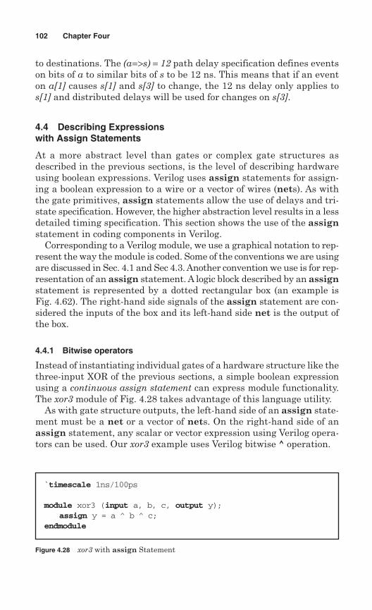
to destinations. The (a=>s) = 12 path delay specification defines eventson bits of a to similar bits of s to be 12 ns. This means that if an eventon a[1] causes s[1] and s[3] to change, the 12 ns delay only applies tos[1] and distributed delays will be used for changes on s[3].
4.4 Describing Expressionswith Assign Statements
At a more abstract level than gates or complex gate structures asdescribed in the previous sections, is the level of describing hardwareusing boolean expressions. Verilog uses assign statements for assign-ing a boolean expression to a wire or a vector of wires (nets). As withthe gate primitives, assign statements allow the use of delays and tri-state specification. However, the higher abstraction level results in a lessdetailed timing specification. This section shows the use of the assignstatement in coding components in Verilog.
Corresponding to a Verilog module, we use a graphical notation to rep-resent the way the module is coded. Some of the conventions we are usingare discussed in Sec. 4.1 and Sec 4.3. Another convention we use is for rep-resentation of an assign statement. A logic block described by an assignstatement is represented by a dotted rectangular box (an example isFig. 4.62). The right-hand side signals of the assign statement are con-sidered the inputs of the box and its left-hand side net is the output ofthe box.
4.4.1 Bitwise operators
Instead of instantiating individual gates of a hardware structure like thethree-input XOR of the previous sections, a simple boolean expressionusing a continuous assign statement can express module functionality.The xor3 module of Fig. 4.28 takes advantage of this language utility.
As with gate structure outputs, the left-hand side of an assign state-ment must be a net or a vector of nets. On the right-hand side of anassign statement, any scalar or vector expression using Verilog opera-tors can be used. Our xor3 example uses Verilog bitwise ^ operation.
102 Chapter Four
Figure 4.28 xor3 with assign Statement
`timescale 1ns/100ps
module xor3 (input a, b, c, output y);assign y = a ^ b ^ c;
endmodule
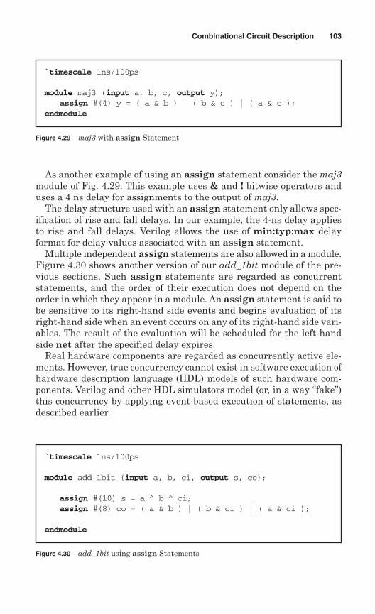
As another example of using an assign statement consider the maj3module of Fig. 4.29. This example uses & and ! bitwise operators anduses a 4 ns delay for assignments to the output of maj3.
The delay structure used with an assign statement only allows spec-ification of rise and fall delays. In our example, the 4-ns delay appliesto rise and fall delays. Verilog allows the use of min:typ:max delayformat for delay values associated with an assign statement.
Multiple independent assign statements are also allowed in a module.Figure 4.30 shows another version of our add_1bit module of the pre-vious sections. Such assign statements are regarded as concurrentstatements, and the order of their execution does not depend on theorder in which they appear in a module. An assign statement is said tobe sensitive to its right-hand side events and begins evaluation of itsright-hand side when an event occurs on any of its right-hand side vari-ables. The result of the evaluation will be scheduled for the left-handside net after the specified delay expires.
Real hardware components are regarded as concurrently active ele-ments. However, true concurrency cannot exist in software execution ofhardware description language (HDL) models of such hardware com-ponents. Verilog and other HDL simulators model (or, in a way “fake”)this concurrency by applying event-based execution of statements, asdescribed earlier.
Combinational Circuit Description 103
Figure 4.29 maj3 with assign Statement
`timescale 1ns/100ps
module maj3 (input a, b, c, output y);assign #(4) y = ( a & b ) | ( b & c ) | ( a & c );
endmodule
Figure 4.30 add_1bit using assign Statements
`timescale 1ns/100ps
module add_1bit (input a, b, ci, output s, co);
assign #(10) s = a ^ b ^ ci;assign #(8) co = ( a & b ) | ( b & ci ) | ( a & ci );
endmodule
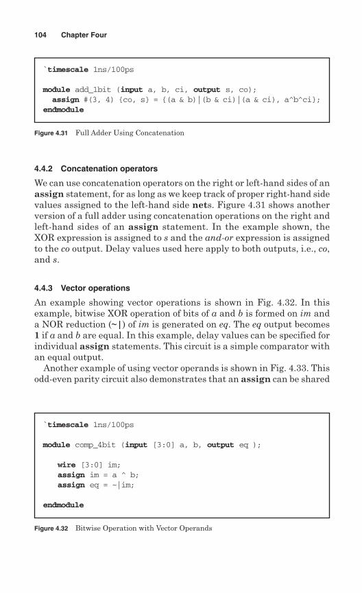
4.4.2 Concatenation operators
We can use concatenation operators on the right or left-hand sides of anassign statement, for as long as we keep track of proper right-hand sidevalues assigned to the left-hand side nets. Figure 4.31 shows anotherversion of a full adder using concatenation operations on the right andleft-hand sides of an assign statement. In the example shown, theXOR expression is assigned to s and the and-or expression is assignedto the co output. Delay values used here apply to both outputs, i.e., co,and s.
4.4.3 Vector operations
An example showing vector operations is shown in Fig. 4.32. In thisexample, bitwise XOR operation of bits of a and b is formed on im anda NOR reduction (~|) of im is generated on eq. The eq output becomes1 if a and b are equal. In this example, delay values can be specified forindividual assign statements. This circuit is a simple comparator withan equal output.
Another example of using vector operands is shown in Fig. 4.33. Thisodd-even parity circuit also demonstrates that an assign can be shared
104 Chapter Four
Figure 4.32 Bitwise Operation with Vector Operands
`timescale 1ns/100ps
module comp_4bit (input [3:0] a, b, output eq );
wire [3:0] im;assign im = a ^ b;assign eq = ~|im;
endmodule
Figure 4.31 Full Adder Using Concatenation
`timescale 1ns/100ps
module add_1bit (input a, b, ci, output s, co);assign #(3, 4) {co, s} = {(a & b)|(b & ci)|(a & ci), a^b^ci};
endmodule
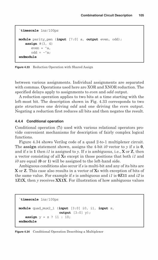
between various assignments. Individual assignments are separatedwith commas. Operations used here are XOR and XNOR reduction. Thespecified delays apply to assignments to even and odd output.
A reduction operation applies to two bits at a time starting with theleft-most bit. The description shown in Fig. 4.33 corresponds to twogate structures one driving odd and one driving the even output.Negating a reduction first reduces all bits and then negates the result.
4.4.4 Conditional operation
Conditional operation (?:) used with various relational operators pro-vide convenient mechanisms for description of fairly complex logicalfunctions.
Figure 4.34 shows Verilog code of a quad 2-to-1 multiplexer circuit.The assign statement shown, assigns the 4-bit i0 vector to y if s is 0,and if s is 1 then i1 is assigned to y. If s is ambiguous, i.e., X or Z, thena vector consisting of all Xs except in those positions that both i1 andi0 are equal (0 or 1) will be assigned to the left-hand side.
Ambiguous conditions also occur if s is multi-bit and any of its bits areX or Z. This case also results in a vector of Xs with exception of bits ofthe same value. For example if s is ambiguous and i1 is 0Z11 and i2 is1Z1X, then y receives XX1X. For illustration of how ambiguous values
Combinational Circuit Description 105
Figure 4.34 Conditional Operation Describing a Multiplexer
`timescale 1ns/100ps
module quad_mux2_1 (input [3:0] i0, i1, input s,output [3:0] y);
assign y = s ? i1 : i0;endmodule
Figure 4.33 Reduction Operation with Shared Assign
`timescale 1ns/100ps
module parity_gen (input [7:0] a, output even, odd);assign #(3, 4)
even = ^a,odd = ~^a;
endmodule
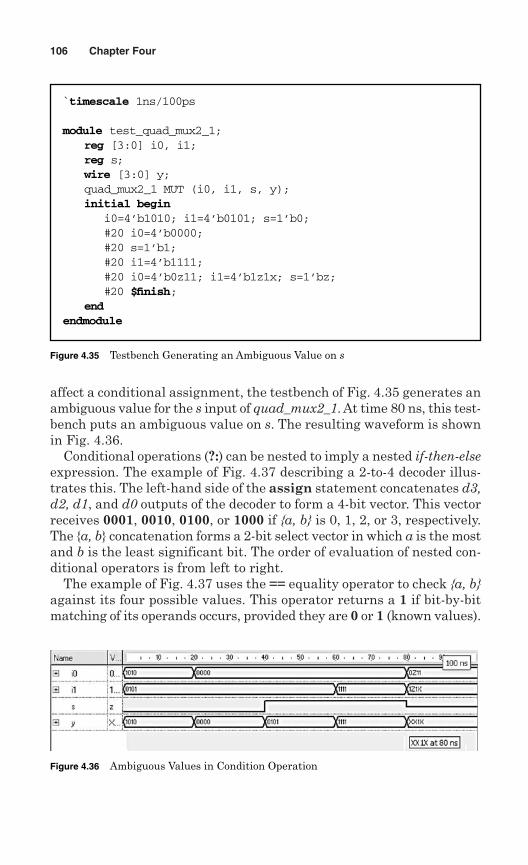
affect a conditional assignment, the testbench of Fig. 4.35 generates anambiguous value for the s input of quad_mux2_1. At time 80 ns, this test-bench puts an ambiguous value on s. The resulting waveform is shownin Fig. 4.36.
Conditional operations (?:) can be nested to imply a nested if-then-elseexpression. The example of Fig. 4.37 describing a 2-to-4 decoder illus-trates this. The left-hand side of the assign statement concatenates d3,d2, d1, and d0 outputs of the decoder to form a 4-bit vector. This vectorreceives 0001, 0010, 0100, or 1000 if {a, b} is 0, 1, 2, or 3, respectively.The {a, b} concatenation forms a 2-bit select vector in which a is the mostand b is the least significant bit. The order of evaluation of nested con-ditional operators is from left to right.
The example of Fig. 4.37 uses the == equality operator to check {a, b}against its four possible values. This operator returns a 1 if bit-by-bitmatching of its operands occurs, provided they are 0 or 1 (known values).
106 Chapter Four
Figure 4.36 Ambiguous Values in Condition Operation
Figure 4.35 Testbench Generating an Ambiguous Value on s
`timescale 1ns/100ps
module test_quad_mux2_1;reg [3:0] i0, i1;reg s;wire [3:0] y;quad_mux2_1 MUT (i0, i1, s, y);initial begin
i0=4’b1010; i1=4’b0101; s=1’b0;#20 i0=4’b0000;#20 s=1’b1;#20 i1=4’b1111;#20 i0=4’b0z11; i1=4’b1z1x; s=1’bz;#20 $finish;
endendmodule
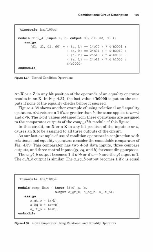
An X or a Z in any bit position of the operands of an equality operatorresults in an X. In Fig. 4.37, the last value 4’b0000 is put on the out-puts if none of the equality checks before it succeed.
Figure 4.38 shows another example of using relational and equalityoperators. a>b returns a 1 if a is greater than b, the same applies to a==band a<b. The 1-bit values obtained from these operations are assignedto the comparator outputs of the comp_4bit module of this figure.
In this circuit, an X or a Z in any bit position of the inputs a or b,causes an X to be assigned to all three outputs of the circuit.
As our last example of use of condition operators in conjunction withrelational and equality operators consider the cascadable comparator ofFig. 4.39. This comparator has two 4-bit data inputs, three compareoutputs, and three control inputs (gt, eq, and lt) for cascading purposes.
The a_gt_b output becomes 1 if a>b or if a==b and the gt input is 1.The a_lt_b output is similar. The a_eq_b output becomes 1 if a is equal
Combinational Circuit Description 107
Figure 4.37 Nested Condition Operations
`timescale 1ns/100ps
module dcd2_4 (input a, b, output d0, d1, d2, d3 );assign
{d3, d2, d1, d0} = ( {a, b} == 2’b00 ) ? 4’b0001 :( {a, b} == 2’b01 ) ? 4’b0010 :( {a, b} == 2’b10 ) ? 4’b0100 :( {a, b} == 2’b11 ) ? 4’b1000 :4’b0000;
endmodule
Figure 4.38 4-bit Comparator Using Relational and Equality Operators
`timescale 1ns/100ps
module comp_4bit ( input [3:0] a, b,output a_gt_b, a_eq_b, a_lt_b);
assigna_gt_b = (a>b),a_eq_b = (a==b),a_lt_b = (a<b);
endmodule
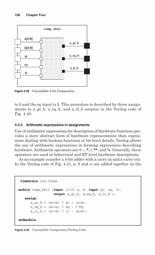
to b and the eq input is 1. This procedure is described by three assign-ments to a_gt_b, a_eq_b, and a_lt_b outputs in the Verilog code ofFig. 4.40.
4.4.5 Arithmetic expressions in assignments
Use of arithmetic expressions for description of hardware functions pro-vides a more abstract form of hardware representation than expres-sions dealing with boolean functions or bit-level details. Verilog allowsthe use of arithmetic expressions in forming expressions describinghardware. Arithmetic operators are +, -, *, /, **, and %. Generally, theseoperators are used in behavioral and RT level hardware descriptions.
As an example consider a 4-bit adder with a carry-in and a carry-out.In the Verilog code of Fig. 4.41, a, b and ci are added together on the
108 Chapter Four
Figure 4.40 Cascadable Comparator Verilog Code
`timescale 1ns/100ps
module comp_4bit (input [3:0] a, b, input gt, eq, lt, output a_gt_b, a_eq_b, a_lt_b );
assigna_gt_b = (a==b) ? gt : (a>b),a_eq_b = (a==b) ? eq : 1’b0,a_lt_b = (a==b) ? lt : (a<b);
endmodule
a[3:0]
b[3:0]
comp_4bit
a_eq_b
a_gt_b
a_lt_b
gt
eq
lt
Figure 4.39 Cascadable 4-bit Comparator
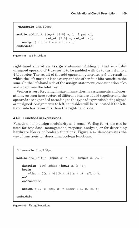
right-hand side of an assign statement. Adding ci that is a 1-bitunsigned operand of + causes it to be padded with 0s to turn it into a4-bit vector. The result of the add operation generates a 5-bit result inwhich the left-most bit is the carry and the other four bits constitute thesum. On the left-hand side of the assign statement, concatenation of coand s captures the 5-bit result.
Verilog is very forgiving in size mismatches in assignments and oper-ations. As seen here vectors of different bits are added together and theoperands are expanded according to the type of expression being signedor unsigned. Assignments to left-hand sides will be truncated if the left-hand side has fewer bits than the right-hand side.
4.4.6 Functions in expressions
Functions help design modularity and reuse. Verilog functions can beused for test data, management, response analysis, or for describinghardware blocks or boolean functions. Figure 4.42 demonstrates theuse of functions for describing boolean functions.
Combinational Circuit Description 109
Figure 4.42 Using Functions
`timescale 1ns/100ps
module add_1bit_f (input a, b, ci, output s, co );
function [1:0] adder (input a, b, c);begin
adder = {(a & b)|(b & c)|(a & c), a^b^c };endendfunction
assign #(3, 4) {co, s} = adder ( a, b, ci );
endmodule
Figure 4.41 A 4-bit Adder
`timescale 1ns/100ps
module add_4bit (input [3:0] a, b, input ci,output [3:0] s, output co);
assign { co, s } = a + b + ci;endmodule
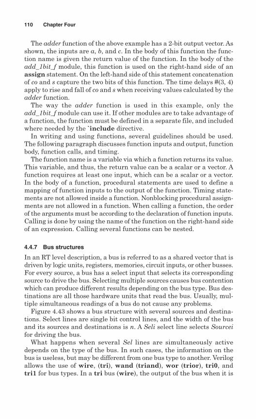
The adder function of the above example has a 2-bit output vector. Asshown, the inputs are a, b, and c. In the body of this function the func-tion name is given the return value of the function. In the body of theadd_1bit_f module, this function is used on the right-hand side of anassign statement. On the left-hand side of this statement concatenationof co and s capture the two bits of this function. The time delays #(3, 4)apply to rise and fall of co and s when receiving values calculated by theadder function.
The way the adder function is used in this example, only theadd_1bit_f module can use it. If other modules are to take advantage ofa function, the function must be defined in a separate file, and includedwhere needed by the `include directive.
In writing and using functions, several guidelines should be used.The following paragraph discusses function inputs and output, functionbody, function calls, and timing.
The function name is a variable via which a function returns its value.This variable, and thus, the return value can be a scalar or a vector. Afunction requires at least one input, which can be a scalar or a vector.In the body of a function, procedural statements are used to define amapping of function inputs to the output of the function. Timing state-ments are not allowed inside a function. Nonblocking procedural assign-ments are not allowed in a function. When calling a function, the orderof the arguments must be according to the declaration of function inputs.Calling is done by using the name of the function on the right-hand sideof an expression. Calling several functions can be nested.
4.4.7 Bus structures
In an RT level description, a bus is referred to as a shared vector that isdriven by logic units, registers, memories, circuit inputs, or other busses.For every source, a bus has a select input that selects its correspondingsource to drive the bus. Selecting multiple sources causes bus contentionwhich can produce different results depending on the bus type. Bus des-tinations are all those hardware units that read the bus. Usually, mul-tiple simultaneous readings of a bus do not cause any problems.
Figure 4.43 shows a bus structure with several sources and destina-tions. Select lines are single bit control lines, and the width of the busand its sources and destinations is n. A Seli select line selects Sourceifor driving the bus.
What happens when several Sel lines are simultaneously activedepends on the type of the bus. In such cases, the information on thebus is useless, but may be different from one bus type to another. Verilogallows the use of wire, (tri), wand (triand), wor (trior), tri0, andtri1 for bus types. In a tri bus (wire), the output of the bus when it is
110 Chapter Four
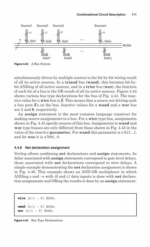
simultaneously driven by multiple sources is the bit-by-bit wiring resultof all its active sources. In a triand bus (wand), this becomes bit-by-bit ANDing of all active sources, and in a trior bus (wor), the functionof each bit of a bus is the OR result of all its active sources. Figure 4.44shows various bus type declarations for the bus of Fig. 4.43. The inac-tive value for a wire bus is Z. This means that a source not driving sucha bus puts Z’s on the bus. Inactive values for a wand and a wor busare 1 and 0, respectively.
An assign statement is the most common language construct formaking source assignments to a bus. For a wire type bus, assignmentsshown in Fig. 4.45 specify sources of this bus. Assignments to wand andwor type busses are only different from those shown in Fig. 4.45 in thevalue of the inactive parameter. For wand this parameter is n’b11...1,and for wor it is n’b00...0.
4.4.8 Net declaration assignment
Verilog allows combining net declarations and assign statements. Asdelay associated with assign statements correspond to gate level delays,those associated with net declarations correspond to wire delays. Asimple example demonstrating the net declaration assignment is shownin Fig. 4.46. This example shows an AND-OR multiplexer in whichANDing s and ~s with i0 and i1 data inputs is done with net declara-tion assignments and ORing the results is done by an assign statement.
Combinational Circuit Description 111
n
n n n n
Source1 Source2 Source3 Sourcem
Dest1 Dest2 Dest j
Sel1 Sel2 Sel3 Selm
BUSA
....
....
Figure 4.43 A Bus System
Figure 4.44 Bus Type Declarations
wire [n-1 : 0] BUSA;. . .wand [n-1 : 0] BUSA;wor [n-1 : 0] BUSA;
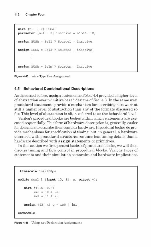
4.5 Behavioral Combinational Descriptions
As discussed before, assign statements of Sec. 4.4 provided a higher-levelof abstraction over primitive based designs of Sec. 4.3. In the same way,procedural statements provide a mechanism for describing hardware atstill a higher level of abstraction than any of the formats discussed sofar. This level of abstraction is often referred to as the behavioral level.
Verilog’s procedural blocks are bodies within which statements are exe-cuted sequentially. This form of hardware description is, generally, easierfor designers to describe their complex hardware. Procedural bodies do pro-vide mechanisms for specification of timing, but, in general, a hardwaredescribed with procedural structures contains less timing details than ahardware described with assign statements or primitives.
In this section we first present basics of procedural blocks, we will thendiscuss timing and flow control in procedural blocks. Various types ofstatements and their simulation semantics and hardware implications
112 Chapter Four
Figure 4.45 wire Type Bus Assignment
wire [n-1 : 0] BUSA;parameter [n-1 : 0] inactive = n’bZZ...Z;
assign BUSA = Sel1 ? Source1 : inactive;
assign BUSA = Sel2 ? Source2 : inactive;...
assign BUSA = Selm ? Sourcem : inactive;
Figure 4.46 Using net Declaration Assignments
`timescale 1ns/100ps
module mux2_1 (input i0, i1, s, output y);
wire #(0.6, 0.8)im0 = i0 & ~s, im1 = i1 & s;
assign #(3, 4) y = im0 | im1;
endmodule
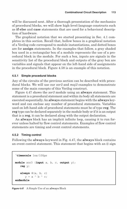
will be discussed next. After a thorough presentation of the mechanicsof procedural blocks, we will show high-level-language constructs suchas if-else and case statements that are used for a behavioral descrip-tion of hardware.
The graphical notation that we started presenting in Sec. 4.1 com-pletes in this section. Recall that, hollow boxes in a graphical notationof a Verilog code correspond to module instantiations, and dotted boxesare for assign statements. In the examples that follow, a gray shadedbox used in a rectangular box of a module represents the use of a pro-cedural block in the module. For such a box, inputs are signals in thesensitivity list of the procedural block and outputs of the gray box arevariables and signals that appear on the left-hand side of assignmentsin the procedural block. Figure 4.58 is an example of this notation.
4.5.1 Simple procedural blocks
Any of the circuits of the previous section can be described with proce-dural blocks. We will use our xor3 and maj3 examples to demonstratesome of the main concepts of this Verilog construct.
Figure 4.47 shows the xor3 module using an always statement. Thisstatement is a procedural statement and within its body all statements areexecuted sequentially. An always statement begins with the always key-word and can enclose any number of procedural statements. Variablesused on left-hand side of procedural statements must be of type reg. Thereg type can be declared separately in the module body or if it is an outputthat is a reg, it can be declared along with the output declaration.
An always block has an implicit infinite loop, causing it to run for-ever unless halted by flow control statements. Examples of flow controlstatements are timing and event control statements.
4.5.2 Timing control
Following the always keyword in Fig. 4.47, the always block containsan event control statement. This statement that begins with an @ sign
Combinational Circuit Description 113
Figure 4.47 A Simple Use of an always Block
`timescale 1ns/100ps
module xor3 (input a, b, c, output y);reg y;
always @(a, b, c)y = a ^ b ^ c;
endmodule
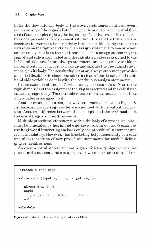
halts the flow into the body of the always statement until an eventoccurs on any of the signals listed, i.e., a or b, or c. An event control (likethat of our example) right at the beginning of an always block is referredto as the procedural block’s sensitivity list. It is said that this block issensitive to events on its sensitivity list. This is like using these samevariables on the right-hand side of an assign statement. When an eventoccurs on a variable on the right-hand side of an assign statement, theright-hand side is calculated and the calculated value is assigned to theleft-hand side net. In an always statement, an event on a variable inits sensitivity list causes it to wake up and execute the procedural state-ment(s) in its body. The sensitivity list of an always statement providesan added flexibility to choose variables instead of the default of all right-hand side variables as it is with the continuous assign statements.
In the example of Fig. 4.47, when an event occurs on a, b, or c, theright-hand side of the assignment to y reg is executed and the calculatedvalue is assigned to y. This variable retains its value until the next timea new value is assigned to it.
Another example for a simple always statement is shown in Fig. 4.48.In this example the reg type for y is specified with its output declara-tion. Another difference between this example and the xor3 module isthe use of begin and end keywords.
Multiple procedural statements within the body of a procedural blockmust be bracketed by begin and end keywords. In our maj3 example,the begin-end bracketing encloses only one procedural statement andis not mandatory. However, this bracketing helps readability of a codeand allows insertion of new procedural statements for module debug-ging or modifications.
An event-control statement that begins with the @ sign is a regularprocedural statement and can appear any where in a procedural block.
114 Chapter Four
Figure 4.48 Majority Circuit Using an always Block
`timescale 1ns/100ps
module maj3 (input a, b, c, output reg y);
always @(a, b, c)begin
y = (a & b) | (b &c) | (a & c);end
endmodule
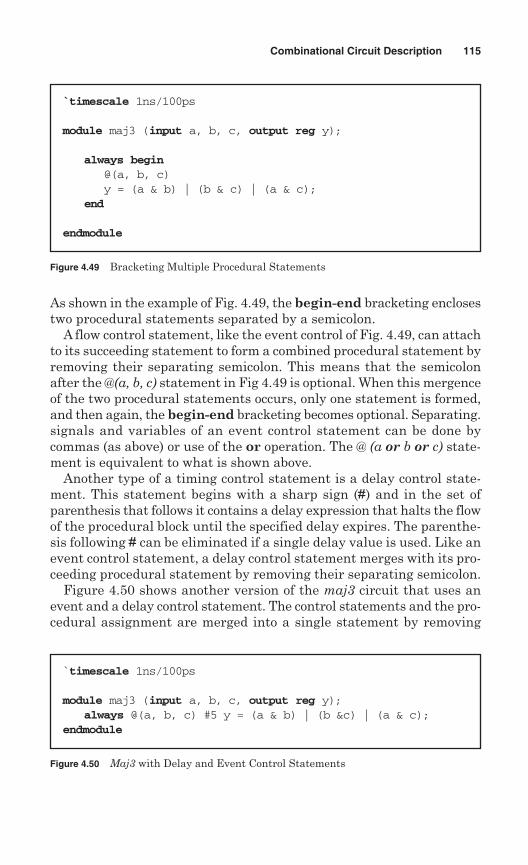
As shown in the example of Fig. 4.49, the begin-end bracketing enclosestwo procedural statements separated by a semicolon.
A flow control statement, like the event control of Fig. 4.49, can attachto its succeeding statement to form a combined procedural statement byremoving their separating semicolon. This means that the semicolonafter the @(a, b, c) statement in Fig 4.49 is optional. When this mergenceof the two procedural statements occurs, only one statement is formed,and then again, the begin-end bracketing becomes optional. Separating.signals and variables of an event control statement can be done bycommas (as above) or use of the or operation. The @ (a or b or c) state-ment is equivalent to what is shown above.
Another type of a timing control statement is a delay control state-ment. This statement begins with a sharp sign (#) and in the set ofparenthesis that follows it contains a delay expression that halts the flowof the procedural block until the specified delay expires. The parenthe-sis following # can be eliminated if a single delay value is used. Like anevent control statement, a delay control statement merges with its pro-ceeding procedural statement by removing their separating semicolon.
Figure 4.50 shows another version of the maj3 circuit that uses anevent and a delay control statement. The control statements and the pro-cedural assignment are merged into a single statement by removing
Combinational Circuit Description 115
Figure 4.49 Bracketing Multiple Procedural Statements
`timescale 1ns/100ps
module maj3 (input a, b, c, output reg y);
always begin@(a, b, c)y = (a & b) | (b & c) | (a & c);
end
endmodule
Figure 4.50 Maj3 with Delay and Event Control Statements
`timescale 1ns/100ps
module maj3 (input a, b, c, output reg y);always @(a, b, c) #5 y = (a & b) | (b &c) | (a & c);
endmodule
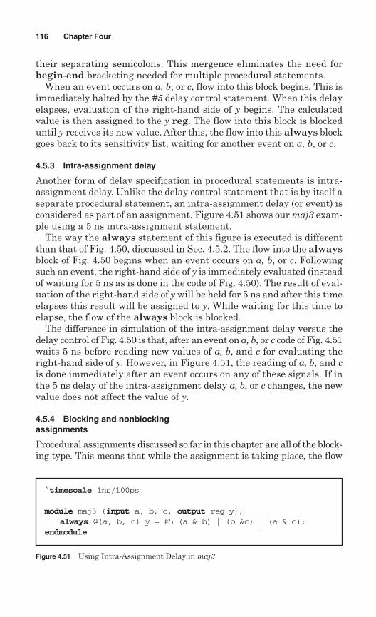
their separating semicolons. This mergence eliminates the need forbegin-end bracketing needed for multiple procedural statements.
When an event occurs on a, b, or c, flow into this block begins. This isimmediately halted by the #5 delay control statement. When this delayelapses, evaluation of the right-hand side of y begins. The calculatedvalue is then assigned to the y reg. The flow into this block is blockeduntil y receives its new value. After this, the flow into this always blockgoes back to its sensitivity list, waiting for another event on a, b, or c.
4.5.3 Intra-assignment delay
Another form of delay specification in procedural statements is intra-assignment delay. Unlike the delay control statement that is by itself aseparate procedural statement, an intra-assignment delay (or event) isconsidered as part of an assignment. Figure 4.51 shows our maj3 exam-ple using a 5 ns intra-assignment statement.
The way the always statement of this figure is executed is differentthan that of Fig. 4.50, discussed in Sec. 4.5.2. The flow into the alwaysblock of Fig. 4.50 begins when an event occurs on a, b, or c. Followingsuch an event, the right-hand side of y is immediately evaluated (insteadof waiting for 5 ns as is done in the code of Fig. 4.50). The result of eval-uation of the right-hand side of y will be held for 5 ns and after this timeelapses this result will be assigned to y. While waiting for this time toelapse, the flow of the always block is blocked.
The difference in simulation of the intra-assignment delay versus thedelay control of Fig. 4.50 is that, after an event on a, b, or c code of Fig. 4.51waits 5 ns before reading new values of a, b, and c for evaluating theright-hand side of y. However, in Figure 4.51, the reading of a, b, and cis done immediately after an event occurs on any of these signals. If inthe 5 ns delay of the intra-assignment delay a, b, or c changes, the newvalue does not affect the value of y.
4.5.4 Blocking and nonblockingassignments
Procedural assignments discussed so far in this chapter are all of the block-ing type. This means that while the assignment is taking place, the flow
116 Chapter Four
Figure 4.51 Using Intra-Assignment Delay in maj3
`timescale 1ns/100ps
module maj3 (input a, b, c, output reg y);always @(a, b, c) y = #5 (a & b) | (b &c) | (a & c);
endmodule
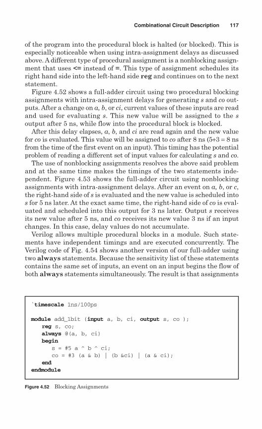
of the program into the procedural block is halted (or blocked). This isespecially noticeable when using intra-assignment delays as discussedabove. A different type of procedural assignment is a nonblocking assign-ment that uses <= instead of =. This type of assignment schedules itsright hand side into the left-hand side reg and continues on to the nextstatement.
Figure 4.52 shows a full-adder circuit using two procedural blockingassignments with intra-assignment delays for generating s and co out-puts. After a change on a, b, or ci, current values of these inputs are readand used for evaluating s. This new value will be assigned to the soutput after 5 ns, while flow into the procedural block is blocked.
After this delay elapses, a, b, and ci are read again and the new valuefor co is evaluated. This value will be assigned to co after 8 ns (5+3 = 8 nsfrom the time of the first event on an input). This timing has the potentialproblem of reading a different set of input values for calculating s and co.
The use of nonblocking assignments resolves the above said problemand at the same time makes the timings of the two statements inde-pendent. Figure 4.53 shows the full-adder circuit using nonblockingassignments with intra-assignment delays. After an event on a, b, or c,the right-hand side of s is evaluated and the new value is scheduled intos for 5 ns later. At the exact same time, the right-hand side of co is eval-uated and scheduled into this output for 3 ns later. Output s receivesits new value after 5 ns, and co receives its new value 3 ns if an inputchanges. In this case, delay values do not accumulate.
Verilog allows multiple procedural blocks in a module. Such state-ments have independent timings and are executed concurrently. TheVerilog code of Fig. 4.54 shows another version of our full-adder usingtwo always statements. Because the sensitivity list of these statementscontains the same set of inputs, an event on an input begins the flow ofboth always statements simultaneously. The result is that assignments
Combinational Circuit Description 117
Figure 4.52 Blocking Assignments
`timescale 1ns/100ps
module add_1bit (input a, b, ci, output s, co );reg s, co;always @(a, b, ci)begin
s = #5 a ^ b ^ ci;co = #3 (a & b) | (b &ci) | (a & ci);
endendmodule
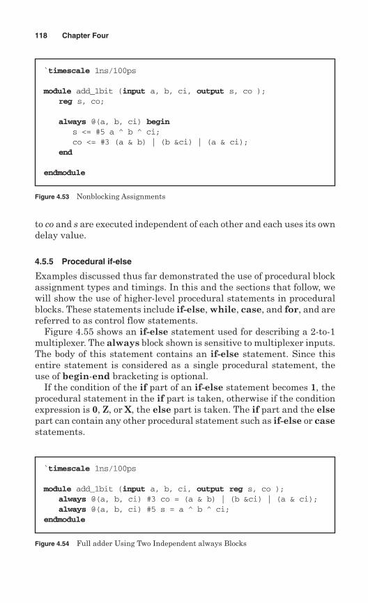
to co and s are executed independent of each other and each uses its owndelay value.
4.5.5 Procedural if-else
Examples discussed thus far demonstrated the use of procedural blockassignment types and timings. In this and the sections that follow, wewill show the use of higher-level procedural statements in proceduralblocks. These statements include if-else, while, case, and for, and arereferred to as control flow statements.
Figure 4.55 shows an if-else statement used for describing a 2-to-1multiplexer. The always block shown is sensitive to multiplexer inputs.The body of this statement contains an if-else statement. Since thisentire statement is considered as a single procedural statement, theuse of begin-end bracketing is optional.
If the condition of the if part of an if-else statement becomes 1, theprocedural statement in the if part is taken, otherwise if the conditionexpression is 0, Z, or X, the else part is taken. The if part and the elsepart can contain any other procedural statement such as if-else or casestatements.
118 Chapter Four
Figure 4.53 Nonblocking Assignments
`timescale 1ns/100ps
module add_1bit (input a, b, ci, output s, co );reg s, co;
always @(a, b, ci) begins <= #5 a ^ b ^ ci;co <= #3 (a & b) | (b &ci) | (a & ci);
end
endmodule
Figure 4.54 Full adder Using Two Independent always Blocks
`timescale 1ns/100ps
module add_1bit (input a, b, ci, output reg s, co );always @(a, b, ci) #3 co = (a & b) | (b &ci) | (a & ci);always @(a, b, ci) #5 s = a ^ b ^ ci;
endmodule
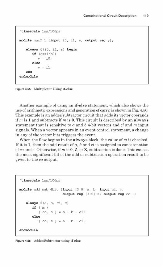
Another example of using an if-else statement, which also shows theuse of arithmetic expressions and generation of carry, is shown in Fig. 4.56.This example is an adder/subtractor circuit that adds its vector operandsif m is 1 and subtracts if m is 0. This circuit is described by an alwaysstatement that is sensitive to a and b 4-bit vectors and ci and m inputsignals. When a vector appears in an event control statement, a changein any of the vector bits triggers the event.
When the flow begins in the always block, the value of m is checked.If it is 1, then the add result of a, b and ci is assigned to concatenationof co and s. Otherwise, if m is 0, Z, or X, subtraction is done. This causesthe most significant bit of the add or subtraction operation result to begiven to the co output.
Combinational Circuit Description 119
Figure 4.55 Multiplexer Using if-else
`timescale 1ns/100ps
module mux2_1 (input i0, i1, s, output reg y);
always @(i0, i1, s) beginif (s==1’b0)
y = i0; else
y = i1;end
endmodule
Figure 4.56 Adder/Subtractor using if-else
`timescale 1ns/100ps
module add_sub_4bit (input [3:0] a, b, input ci, m,output reg [3:0] s, output reg co );
always @(a, b, ci, m)if ( m )
{ co, s } = a + b + ci;else
{ co, s } = a - b - ci;
endmodule
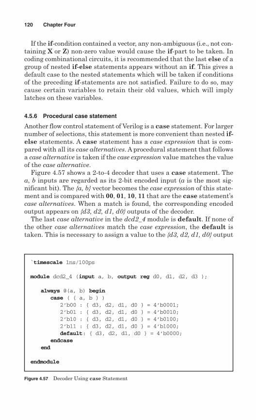
If the if-condition contained a vector, any non-ambiguous (i.e., not con-taining X or Z) non-zero value would cause the if-part to be taken. Incoding combinational circuits, it is recommended that the last else of agroup of nested if-else statements appears without an if. This gives adefault case to the nested statements which will be taken if conditionsof the preceding if-statements are not satisfied. Failure to do so, maycause certain variables to retain their old values, which will implylatches on these variables.
4.5.6 Procedural case statement
Another flow control statement of Verilog is a case statement. For largernumber of selections, this statement is more convenient than nested if-else statements. A case statement has a case expression that is com-pared with all its case alternatives. A procedural statement that followsa case alternative is taken if the case expression value matches the valueof the case alternative.
Figure 4.57 shows a 2-to-4 decoder that uses a case statement. Thea, b inputs are regarded as its 2-bit encoded input (a is the most sig-nificant bit). The {a, b} vector becomes the case expression of this state-ment and is compared with 00, 01, 10, 11 that are the case statement’scase alternatives. When a match is found, the corresponding encodedoutput appears on {d3, d2, d1, d0} outputs of the decoder.
The last case alternative in the dcd2_4 module is default. If none ofthe other case alternatives match the case expression, the default istaken. This is necessary to assign a value to the {d3, d2, d1, d0} output
120 Chapter Four
Figure 4.57 Decoder Using case Statement
`timescale 1ns/100ps
module dcd2_4 (input a, b, output reg d0, d1, d2, d3 );
always @(a, b) begincase ( { a, b } )
2’b00 : { d3, d2, d1, d0 } = 4’b0001;2’b01 : { d3, d2, d1, d0 } = 4’b0010;2’b10 : { d3, d2, d1, d0 } = 4’b0100;2’b11 : { d3, d2, d1, d0 } = 4’b1000;default: { d3, d2, d1, d0 } = 4’b0000;
endcaseend
endmodule
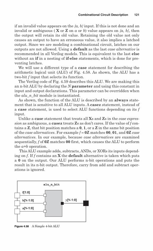
if an invalid value appears on the {a, b} input. If this is not done and aninvalid or ambiguous ( X or Z on a or b) value appears on {a, b}, thenthe output will retain its old value. Retaining the old value not onlycauses an output to have an erroneous value, it also implies a latchedoutput. Since we are modeling a combinational circuit, latches on ouroutputs are not allowed. Using a default as the last case alternative isrecommended in all Verilog models. This is equivalent to the last elsewithout an if in a nesting of if-else statements, which is done for pre-venting latches.
We will use a different type of a case statement for describing thearithmetic logical unit (ALU) of Fig. 4.58. As shown, the ALU has atwo-bit f input that selects its function.
The Verilog code of Fig. 4.59 describes this ALU. We are making thisan n-bit ALU by declaring the N parameter and using this constant ininput and output declarations. This parameter can be overridden whenthe alu_n_bit module is instantiated.
As shown, the function of the ALU is described by an always state-ment that is sensitive to all ALU inputs. A casez statement, instead ofa case statement, is used to select ALU functions depending on its finput.
Unlike a case statement that treats all Xs and Zs in the case expres-sion as ambiguous, a casez treats Zs as don’t cares. If the value of f con-tains a Z, that bit position matches a 0, 1, or a Z in the same bit positionof the case alternatives. For example f = 0Z matches 00, 01, and 0Z casealternatives. In our example, because case alternatives are examinedsequentially, f of 0Z matches 00 first, which causes the ALU to performthe a+b operation.
This ALU example adds, subtracts, ANDs, or XORs its inputs depend-ing on f. If f contains an X the default alternative is taken which putsa 0 on the output. Our ALU performs n-bit operations and puts theresult in its n-bit output. Therefore, carry from add and subtract oper-ations is ignored.
Combinational Circuit Description 121
a[N-1:0]
b[N-1:0]
alu_n_bit
y[N-1:0]
f[1:0]
Figure 4.58 A Simple 4-bit ALU
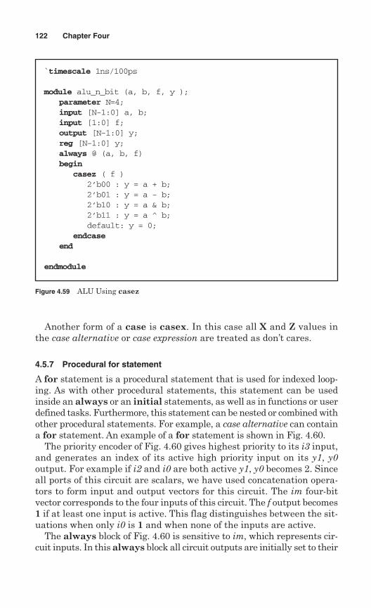
Another form of a case is casex. In this case all X and Z values inthe case alternative or case expression are treated as don’t cares.
4.5.7 Procedural for statement
A for statement is a procedural statement that is used for indexed loop-ing. As with other procedural statements, this statement can be usedinside an always or an initial statements, as well as in functions or userdefined tasks. Furthermore, this statement can be nested or combined withother procedural statements. For example, a case alternative can containa for statement. An example of a for statement is shown in Fig. 4.60.
The priority encoder of Fig. 4.60 gives highest priority to its i3 input,and generates an index of its active high priority input on its y1, y0output. For example if i2 and i0 are both active y1, y0 becomes 2. Sinceall ports of this circuit are scalars, we have used concatenation opera-tors to form input and output vectors for this circuit. The im four-bitvector corresponds to the four inputs of this circuit. The f output becomes1 if at least one input is active. This flag distinguishes between the sit-uations when only i0 is 1 and when none of the inputs are active.
The always block of Fig. 4.60 is sensitive to im, which represents cir-cuit inputs. In this always block all circuit outputs are initially set to their
122 Chapter Four
Figure 4.59 ALU Using casez
`timescale 1ns/100ps
module alu_n_bit (a, b, f, y );parameter N=4;input [N-1:0] a, b;input [1:0] f;output [N-1:0] y;reg [N-1:0] y;always @ (a, b, f)begin
casez ( f )2’b00 : y = a + b;2’b01 : y = a - b;2’b10 : y = a & b;2’b11 : y = a ^ b;default: y = 0;
endcaseend
endmodule
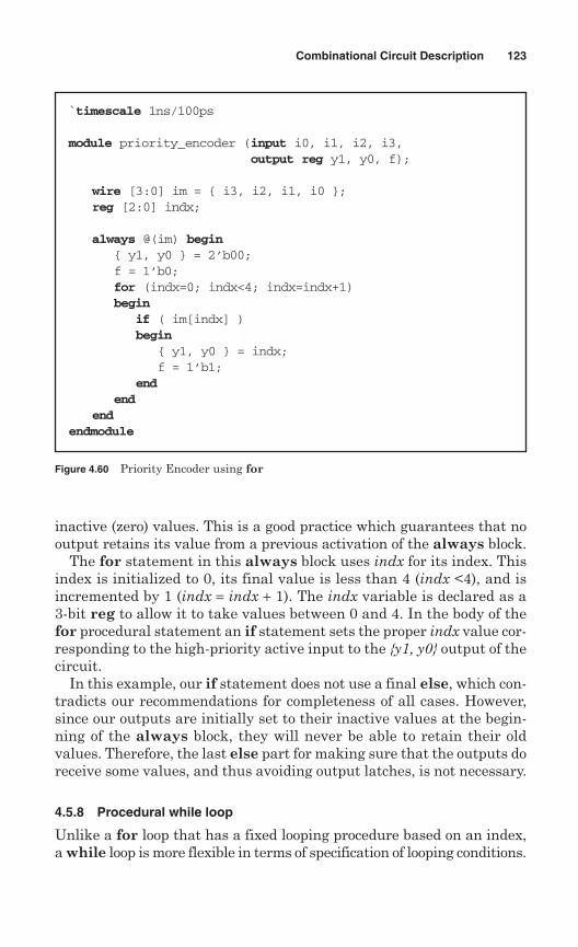
inactive (zero) values. This is a good practice which guarantees that nooutput retains its value from a previous activation of the always block.
The for statement in this always block uses indx for its index. Thisindex is initialized to 0, its final value is less than 4 (indx <4), and isincremented by 1 (indx = indx + 1). The indx variable is declared as a3-bit reg to allow it to take values between 0 and 4. In the body of thefor procedural statement an if statement sets the proper indx value cor-responding to the high-priority active input to the {y1, y0} output of thecircuit.
In this example, our if statement does not use a final else, which con-tradicts our recommendations for completeness of all cases. However,since our outputs are initially set to their inactive values at the begin-ning of the always block, they will never be able to retain their oldvalues. Therefore, the last else part for making sure that the outputs doreceive some values, and thus avoiding output latches, is not necessary.
4.5.8 Procedural while loop
Unlike a for loop that has a fixed looping procedure based on an index,a while loop is more flexible in terms of specification of looping conditions.
Combinational Circuit Description 123
Figure 4.60 Priority Encoder using for
`timescale 1ns/100ps
module priority_encoder (input i0, i1, i2, i3, output reg y1, y0, f);
wire [3:0] im = { i3, i2, i1, i0 };reg [2:0] indx;
always @(im) begin{ y1, y0 } = 2’b00;f = 1’b0;for (indx=0; indx<4; indx=indx+1)begin
if ( im[indx] )begin
{ y1, y0 } = indx;f = 1’b1;
endend
endendmodule
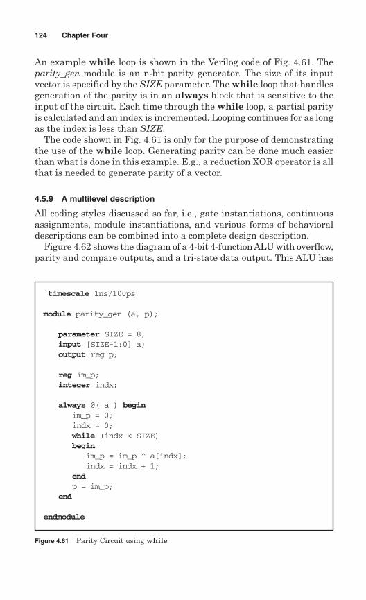
An example while loop is shown in the Verilog code of Fig. 4.61. Theparity_gen module is an n-bit parity generator. The size of its inputvector is specified by the SIZE parameter. The while loop that handlesgeneration of the parity is in an always block that is sensitive to theinput of the circuit. Each time through the while loop, a partial parityis calculated and an index is incremented. Looping continues for as longas the index is less than SIZE.
The code shown in Fig. 4.61 is only for the purpose of demonstratingthe use of the while loop. Generating parity can be done much easierthan what is done in this example. E.g., a reduction XOR operator is allthat is needed to generate parity of a vector.
4.5.9 A multilevel description
All coding styles discussed so far, i.e., gate instantiations, continuousassignments, module instantiations, and various forms of behavioraldescriptions can be combined into a complete design description.
Figure 4.62 shows the diagram of a 4-bit 4-function ALU with overflow,parity and compare outputs, and a tri-state data output. This ALU has
124 Chapter Four
Figure 4.61 Parity Circuit using while
`timescale 1ns/100ps
module parity_gen (a, p);
parameter SIZE = 8;input [SIZE-1:0] a;output reg p;
reg im_p;integer indx;
always @( a ) beginim_p = 0;indx = 0;while (indx < SIZE)begin
im_p = im_p ^ a[indx];indx = indx + 1;
endp = im_p;
end
endmodule
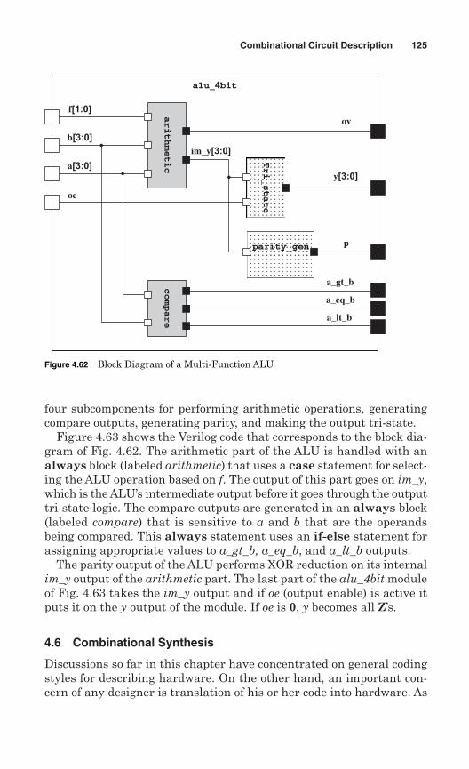
four subcomponents for performing arithmetic operations, generatingcompare outputs, generating parity, and making the output tri-state.
Figure 4.63 shows the Verilog code that corresponds to the block dia-gram of Fig. 4.62. The arithmetic part of the ALU is handled with analways block (labeled arithmetic) that uses a case statement for select-ing the ALU operation based on f. The output of this part goes on im_y,which is the ALU’s intermediate output before it goes through the outputtri-state logic. The compare outputs are generated in an always block(labeled compare) that is sensitive to a and b that are the operandsbeing compared. This always statement uses an if-else statement forassigning appropriate values to a_gt_b, a_eq_b, and a_lt_b outputs.
The parity output of the ALU performs XOR reduction on its internalim_y output of the arithmetic part. The last part of the alu_4bit moduleof Fig. 4.63 takes the im_y output and if oe (output enable) is active itputs it on the y output of the module. If oe is 0, y becomes all Z’s.
4.6 Combinational Synthesis
Discussions so far in this chapter have concentrated on general codingstyles for describing hardware. On the other hand, an important con-cern of any designer is translation of his or her code into hardware. As
Combinational Circuit Description 125
a[3:0]
alu_4bit
im_y[3:0]
ov
oe
y[3:0]
p
a_gt_b
a_eq_b
a_lt_b
b[3:0]
f[1:0] arithmetic
compare
Tri_state
parity_gen
Figure 4.62 Block Diagram of a Multi-Function ALU
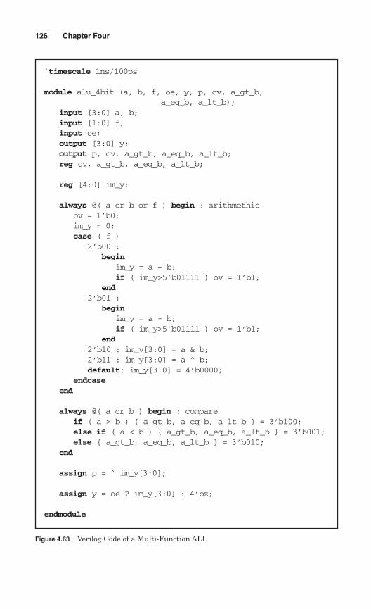
126 Chapter Four
Figure 4.63 Verilog Code of a Multi-Function ALU
`timescale 1ns/100ps
module alu_4bit (a, b, f, oe, y, p, ov, a_gt_b,a_eq_b, a_lt_b);
input [3:0] a, b;input [1:0] f;input oe;output [3:0] y;output p, ov, a_gt_b, a_eq_b, a_lt_b;reg ov, a_gt_b, a_eq_b, a_lt_b;
reg [4:0] im_y;
always @( a or b or f ) begin : arithmethicov = 1’b0;im_y = 0;case ( f )
2’b00 : begin
im_y = a + b;if ( im_y>5’b01111 ) ov = 1’b1;
end2’b01 :
beginim_y = a - b;if ( im_y>5’b01111 ) ov = 1’b1;
end2’b10 : im_y[3:0] = a & b; 2’b11 : im_y[3:0] = a ^ b;default: im_y[3:0] = 4’b0000;
endcaseend
always @( a or b ) begin : compareif ( a > b ) { a_gt_b, a_eq_b, a_lt_b } = 3’b100;else if ( a < b ) { a_gt_b, a_eq_b, a_lt_b } = 3’b001;else { a_gt_b, a_eq_b, a_lt_b } = 3’b010;
end
assign p = ^ im_y[3:0];
assign y = oe ? im_y[3:0] : 4’bz;
endmodule
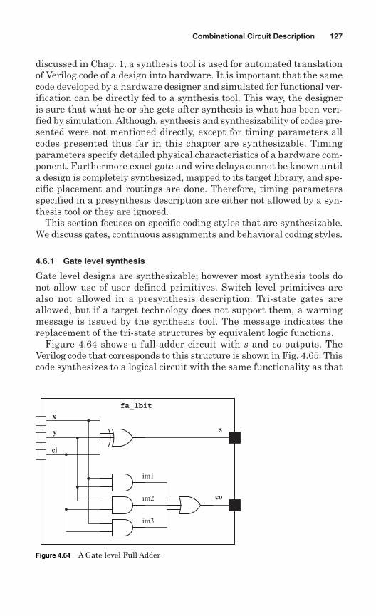
discussed in Chap. 1, a synthesis tool is used for automated translationof Verilog code of a design into hardware. It is important that the samecode developed by a hardware designer and simulated for functional ver-ification can be directly fed to a synthesis tool. This way, the designeris sure that what he or she gets after synthesis is what has been veri-fied by simulation. Although, synthesis and synthesizability of codes pre-sented were not mentioned directly, except for timing parameters allcodes presented thus far in this chapter are synthesizable. Timingparameters specify detailed physical characteristics of a hardware com-ponent. Furthermore exact gate and wire delays cannot be known untila design is completely synthesized, mapped to its target library, and spe-cific placement and routings are done. Therefore, timing parametersspecified in a presynthesis description are either not allowed by a syn-thesis tool or they are ignored.
This section focuses on specific coding styles that are synthesizable.We discuss gates, continuous assignments and behavioral coding styles.
4.6.1 Gate level synthesis
Gate level designs are synthesizable; however most synthesis tools donot allow use of user defined primitives. Switch level primitives arealso not allowed in a presynthesis description. Tri-state gates areallowed, but if a target technology does not support them, a warningmessage is issued by the synthesis tool. The message indicates thereplacement of the tri-state structures by equivalent logic functions.
Figure 4.64 shows a full-adder circuit with s and co outputs. TheVerilog code that corresponds to this structure is shown in Fig. 4.65. Thiscode synthesizes to a logical circuit with the same functionality as that
Combinational Circuit Description 127
xfa_1bit
ci
co
sy
im1
im2
im3
Figure 4.64 A Gate level Full Adder
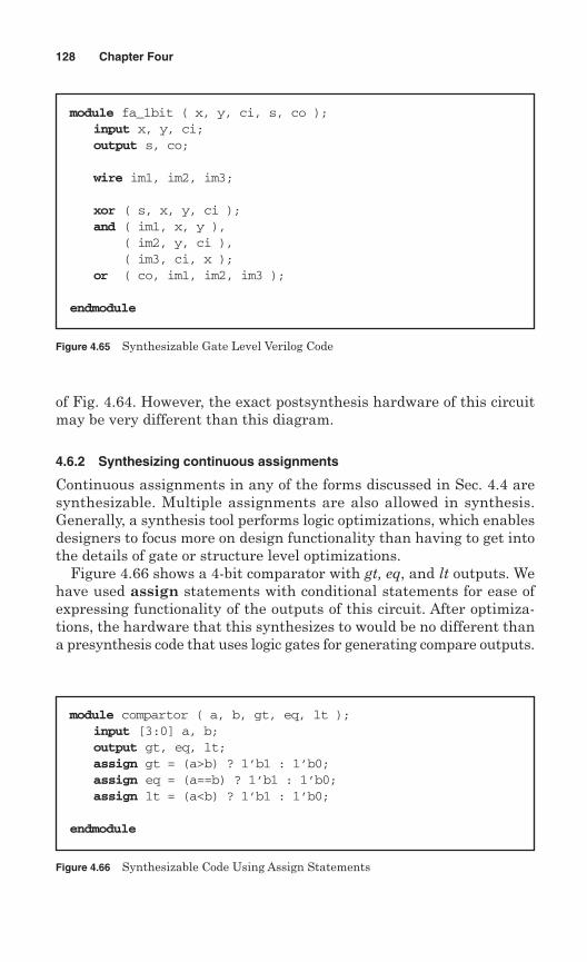
of Fig. 4.64. However, the exact postsynthesis hardware of this circuitmay be very different than this diagram.
4.6.2 Synthesizing continuous assignments
Continuous assignments in any of the forms discussed in Sec. 4.4 aresynthesizable. Multiple assignments are also allowed in synthesis.Generally, a synthesis tool performs logic optimizations, which enablesdesigners to focus more on design functionality than having to get intothe details of gate or structure level optimizations.
Figure 4.66 shows a 4-bit comparator with gt, eq, and lt outputs. Wehave used assign statements with conditional statements for ease ofexpressing functionality of the outputs of this circuit. After optimiza-tions, the hardware that this synthesizes to would be no different thana presynthesis code that uses logic gates for generating compare outputs.
128 Chapter Four
Figure 4.65 Synthesizable Gate Level Verilog Code
module fa_1bit ( x, y, ci, s, co );input x, y, ci;output s, co;
wire im1, im2, im3;
xor ( s, x, y, ci );and ( im1, x, y ),
( im2, y, ci ),( im3, ci, x );
or ( co, im1, im2, im3 );
endmodule
Figure 4.66 Synthesizable Code Using Assign Statements
module compartor ( a, b, gt, eq, lt );input [3:0] a, b;output gt, eq, lt;assign gt = (a>b) ? 1’b1 : 1’b0;assign eq = (a==b) ? 1’b1 : 1’b0;assign lt = (a<b) ? 1’b1 : 1’b0;
endmodule
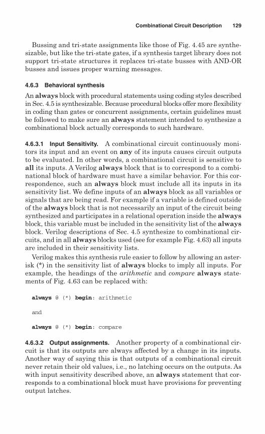
Bussing and tri-state assignments like those of Fig. 4.45 are synthe-sizable, but like the tri-state gates, if a synthesis target library does notsupport tri-state structures it replaces tri-state busses with AND-ORbusses and issues proper warning messages.
4.6.3 Behavioral synthesis
An always block with procedural statements using coding styles describedin Sec. 4.5 is synthesizable. Because procedural blocks offer more flexibilityin coding than gates or concurrent assignments, certain guidelines mustbe followed to make sure an always statement intended to synthesize acombinational block actually corresponds to such hardware.
4.6.3.1 Input Sensitivity. A combinational circuit continuously moni-tors its input and an event on any of its inputs causes circuit outputsto be evaluated. In other words, a combinational circuit is sensitive toall its inputs. A Verilog always block that is to correspond to a combi-national block of hardware must have a similar behavior. For this cor-respondence, such an always block must include all its inputs in itssensitivity list. We define inputs of an always block as all variables orsignals that are being read. For example if a variable is defined outsideof the always block that is not necessarily an input of the circuit beingsynthesized and participates in a relational operation inside the alwaysblock, this variable must be included in the sensitivity list of the alwaysblock. Verilog descriptions of Sec. 4.5 synthesize to combinational cir-cuits, and in all always blocks used (see for example Fig. 4.63) all inputsare included in their sensitivity lists.
Verilog makes this synthesis rule easier to follow by allowing an aster-isk (*) in the sensitivity list of always blocks to imply all inputs. Forexample, the headings of the arithmetic and compare always state-ments of Fig. 4.63 can be replaced with:
always @ (*) begin: arithmetic
and
always @ (*) begin: compare
4.6.3.2 Output assignments. Another property of a combinational cir-cuit is that its outputs are always affected by a change in its inputs.Another way of saying this is that outputs of a combinational circuitnever retain their old values, i.e., no latching occurs on the outputs. Aswith input sensitivity described above, an always statement that cor-responds to a combinational block must have provisions for preventingoutput latches.
Combinational Circuit Description 129
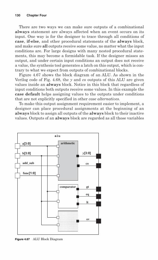
There are two ways we can make sure outputs of a combinationalalways statement are always affected when an event occurs on itsinput. One way is for the designer to trace through all conditions ofcase, if-else, and other procedural statements of the always block,and make sure all outputs receive some value, no matter what the inputconditions are. For large designs with many nested procedural state-ments, this may become a formidable task. If the designer misses anoutput, and under certain input conditions an output does not receivea value, the synthesis tool generates a latch on this output, which is con-trary to what we expect from outputs of combinational blocks.
Figure 4.67 shows the block diagram of an ALU. As shown in theVerilog code of Fig. 4.68, the y and co outputs of this ALU are givenvalues inside an always block. Notice in this block that regardless ofinput conditions both outputs receive some values. In this example thecase default helps assigning values to the outputs under conditionsthat are not explicitly specified in other case alternatives.
To make this output assignment requirement easier to implement, adesigner can place procedural assignments at the beginning of analways block to assign all outputs of the always block to their inactivevalues. Outputs of an always block are regarded as all those variables
130 Chapter Four
a[3:0]
b[3:0] y[3:0]
co
alu
add_sub
func[1:0]
gt
eq
lt
ov
comparator
arithmetic
Figure 4.67 ALU Block Diagram
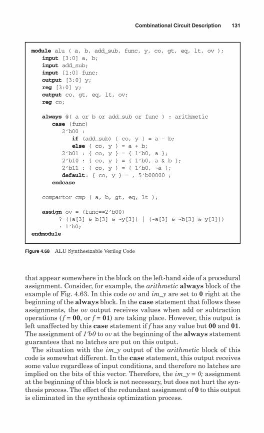
that appear somewhere in the block on the left-hand side of a proceduralassignment. Consider, for example, the arithmetic always block of theexample of Fig. 4.63. In this code ov and im_y are set to 0 right at thebeginning of the always block. In the case statement that follows theseassignments, the ov output receives values when add or subtractionoperations ( f = 00, or f = 01) are taking place. However, this output isleft unaffected by this case statement if f has any value but 00 and 01.The assignment of 1'b0 to ov at the beginning of the always statementguarantees that no latches are put on this output.
The situation with the im_y output of the arithmetic block of thiscode is somewhat different. In the case statement, this output receivessome value regardless of input conditions, and therefore no latches areimplied on the bits of this vector. Therefore, the im_y = 0; assignmentat the beginning of this block is not necessary, but does not hurt the syn-thesis process. The effect of the redundant assignment of 0 to this outputis eliminated in the synthesis optimization process.
Combinational Circuit Description 131
Figure 4.68 ALU Synthesizable Verilog Code
module alu ( a, b, add_sub, func, y, co, gt, eq, lt, ov );input [3:0] a, b;input add_sub;input [1:0] func;output [3:0] y;reg [3:0] y;output co, gt, eq, lt, ov;reg co;
always @( a or b or add_sub or func ) : arithmeticcase (func)
2’b00 : if (add_sub) { co, y } = a - b;else { co, y } = a + b;
2’b01 : { co, y } = { 1’b0, a };2’b10 : { co, y } = { 1’b0, a & b };2’b11 : { co, y } = { 1’b0, ~a };default: { co, y } = , 5’b00000 ;
endcase
compartor cmp ( a, b, gt, eq, lt );
assign ov = (func==2’b00) ? ((a[3] & b[3] & ~y[3]) | (~a[3] & ~b[3] & y[3])) : 1’b0;
endmodule
4.6.4 Mixed synthesis
Gate level, module instantiations, assign statements and always blockscan all coexist in a synthesizable description. For example the code ofFig. 4.68 has an always block that assigns values to co and y outputsof the ALU. Instantiation of the comparator module of Fig. 4.66 provideshardware for driving the compare outputs of the ALU. The last state-ment in the synthesizable code of the alu module is an assign statementthat generates logic for driving the ov output. Note that overflow onlyoccurs if the ALU is performing an add operation. Therefore assign-ment to ov is conditioned by func == 2’b00, where 2’b00 is the add opcode.
4.7 Summary
Although the focus of this chapter was primarily on combinational cir-cuits, most language constructs used for combinational and sequentialcircuits were presented. Therefore this chapter can be regarded as ourmain chapter presenting the Verilog language in an example orientedfashion. In addition to constructs that directly correspond to hardwarestructures, this chapter also presented constructs for specification oftiming of a hardware unit. Obviously, such constructs cannot be usedin designs for synthesis.
Problems
4.1 Write a Verilog description for the following function.
f (A, B, C, D) = Σm(0, 2, 4, 5, 6, 7, 9, 10, 11), d(1, 13)
4.2 Write Verilog code for a 4-to-1 multiplexer with a tri-state output and anactive low OutputEnable input. The multiplexer has four data inputs (d0, d1,d2, d3) and two select inputs (s1, s0). Use case and if statements.
4.3 Use two of the multiplexers of Prob. 4.2 to build an 8-to-1 multiplexer.
4.4 Use the 8-to-1 multiplexer of Prob. 4.3 to implement the function ofProblem 4.1.
4.5 Show Verilog code for a cascadable 4-to-2 priority encoder. Your circuitshould have an enable input, four data inputs, an enable output, an interruptoutput, and two source id outputs. All inputs and outputs must be active high.For cascading purposes and to be able to use wired-OR logic, use tri-state foryour id outputs. Adjust the details of your design for a better cascading capability.
4.6 Write a Verilog description for a 4-bit adder-subtractor that adds when asis 1 and subtracts when as is 0.
132 Chapter Four
4.7 Write a Verilog function to implement a 4-bit BCD to seven-segment display(BDC_to_7Seg) converter. Use vector inputs and outputs. Number your outputsegments from 0 to 6 in clock-wise direction starting with the top segment andending with the middle segment.
4.8 Show gate level details of the circuit described by the following Verilog code.
Combinational Circuit Description 133
module infer (q, d, e, c);input d, c;output q;reg q;
always @(c, d, e)if (c == 1 && e == 0) q = d; else q = 1;
endmodule
s2 s1 S0 Function
0 0 0 A add B0 0 1 A sub B0 1 0 A add 2*B0 1 1 A sub 2*B1 0 0 A * B (4-bit)1 0 1 min (A, B)1 1 0 Abs (A)1 1 1 B
4.9 Consider two 4-bit binary numbers A and B. Bits of A are a3, a2, a1, anda0, and bits of B are b3, b2, b1, and b0. A is greater than B if a3 is 1 and b3 is0, but if a3 and b3 are the same, then if a2 is 1 and b2 is 0, we can determinethat A is greater than B. This evaluation continues until a0 and b0 areconsidered. If a0 and b0 are equal then A and B are equal. Using discrete gatesand Verilog gate primitives build a 4-bit comparator that generates a 1 on itsGT output when its 4-bit input A is greater than its B input, and a 1 on its EQoutput when A and B are equal. Use the generate statement and other Verilogiterative logic support structures.
4.10 Using the comparator of Prob. 4.9 and discrete logic gates, build a MINcircuit that takes two 4-bit inputs and puts the smaller of its two inputs on itsoutput. Write the Verilog description of this circuit.
4.11 Write a Verilog description for a multiplier bit. Using this multiplier bitwrite a Verilog code for a 4×4 array multiplier. Then, using the 4×4 multiplierdesign an ALU that performs eight functions according to the following table.The data inputs of the ALU are 8 bits. Use always blocks and case statementsin your Verilog description.

Suggested Reading
Bhasker, J., Verilog HDL Synthesis, A Practical Primer, Star Galaxy Pub, 1998, ISBN:0965039153.
Brown S., and Z. Vranesic, Fundamentals of Digital Logic with Verilog Design, McGraw-Hill, New York, 2002, ISBN: 0-07-283878-7.
IEEE Std 1364-2001, IEEE Standard Verilog Language Reference Manual, SH94921-TBR (print) SS94921-TBR (electronic), ISBN 0-7381-2827-9 (print and electronic),2001.
Navabi, Z., Digital Design and Implementation with Field Programmable Devices, KluwerAcademic Publishers, Boston, 2005, ISBN: 1-4020-8011-5.
Navabi, Z., Verilog Computer-Based Training Course, CBT CD with hardcopy User’smanual, McGraw-Hill, New York, 2002, ISBN 0-07-137473-6.
Palnitkar, S., Verilog HDL, 2d ed, Prentice Hall PTR, New Jersey, 2003, ISBN: 0130449113.Thomas, P. R., and P. Moorby, The Verilog® Hardware Description Language, Springer,
Boston, 2002, ISBN: 1402070896.
134 Chapter Four
Chapter
5Sequential Circuit Description
Based on the material of Chap. 3, the previous chapter discussed waysof modeling timing and functionality of combinational circuits. Thischapter follows a similar flow as that of Chap. 4, but concentrates onusing Verilog constructs for description of sequential circuits. For thesake of completeness we discuss use of gate level and assignments fordescribing memory elements; however, most of our attention will begiven to modeling such parts with procedural statements. Because mostof Verilog language constructs have already been discussed in conjunc-tion with the combinational circuits, this chapter focuses less on languageaspects and more on hardware modeling. Furthermore, timing-relatedissues of the language, as discussed in Chap. 4, apply as well to sequen-tial circuits and will not be discussed here.
The next section in this chapter discusses hardware properties thatmake a logic circuit store data. Section 5.2 shows ways of describingbasic memory components. Based on models discussed, Sec. 5.3 showsVerilog description of functions with storage capability such as countersand shift registers. This will be followed by state machine and con-troller modeling, and finally as in Chap. 4, we will have a discussion ofmodeling for synthesis.
5.1 Sequential Models
In digital circuits, storage of data is done either by feedback, or by gatecapacitances that are refreshed frequently. Verilog provides languageconstructs for building memory elements using both these schemes.However, more abstract models also exist and are used in most sequen-tial circuit models.
135
Copyright © 2006 by The McGraw-Hill Publishing Companies, Inc. Click here for terms of use.
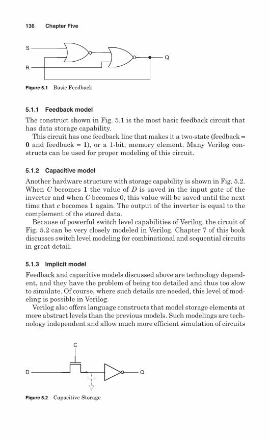
5.1.1 Feedback model
The construct shown in Fig. 5.1 is the most basic feedback circuit thathas data storage capability.
This circuit has one feedback line that makes it a two-state (feedback =0 and feedback = 1), or a 1-bit, memory element. Many Verilog con-structs can be used for proper modeling of this circuit.
5.1.2 Capacitive model
Another hardware structure with storage capability is shown in Fig. 5.2.When C becomes 1 the value of D is saved in the input gate of theinverter and when C becomes 0, this value will be saved until the nexttime that c becomes 1 again. The output of the inverter is equal to thecomplement of the stored data.
Because of powerful switch level capabilities of Verilog, the circuit ofFig. 5.2 can be very closely modeled in Verilog. Chapter 7 of this bookdiscusses switch level modeling for combinational and sequential circuitsin great detail.
5.1.3 Implicit model
Feedback and capacitive models discussed above are technology depend-ent, and they have the problem of being too detailed and thus too slowto simulate. Of course, where such details are needed, this level of mod-eling is possible in Verilog.
Verilog also offers language constructs that model storage elements atmore abstract levels than the previous models. Such modelings are tech-nology independent and allow much more efficient simulation of circuits
136 Chapter Five
S
R
Q
Figure 5.1 Basic Feedback
Figure 5.2 Capacitive Storage
D
C
Q
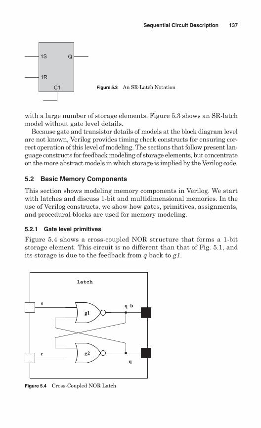
with a large number of storage elements. Figure 5.3 shows an SR-latchmodel without gate level details.
Because gate and transistor details of models at the block diagram levelare not known, Verilog provides timing check constructs for ensuring cor-rect operation of this level of modeling. The sections that follow present lan-guage constructs for feedback modeling of storage elements, but concentrateon the more abstract models in which storage is implied by the Verilog code.
5.2 Basic Memory Components
This section shows modeling memory components in Verilog. We startwith latches and discuss 1-bit and multidimensional memories. In theuse of Verilog constructs, we show how gates, primitives, assignments,and procedural blocks are used for memory modeling.
5.2.1 Gate level primitives
Figure 5.4 shows a cross-coupled NOR structure that forms a 1-bitstorage element. This circuit is no different than that of Fig. 5.1, andits storage is due to the feedback from q back to g1.
Sequential Circuit Description 137
1S
1R
Q
C1 Figure 5.3 An SR-Latch Notation
s
rq
g1
g2
q_b
latch
Figure 5.4 Cross-Coupled NOR Latch
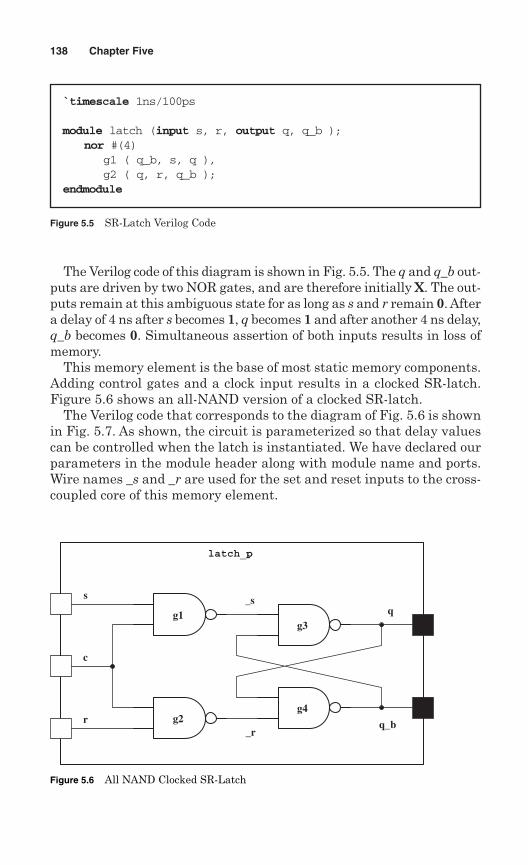
The Verilog code of this diagram is shown in Fig. 5.5. The q and q_b out-puts are driven by two NOR gates, and are therefore initially X. The out-puts remain at this ambiguous state for as long as s and r remain 0. Aftera delay of 4 ns after s becomes 1, q becomes 1 and after another 4 ns delay,q_b becomes 0. Simultaneous assertion of both inputs results in loss ofmemory.
This memory element is the base of most static memory components.Adding control gates and a clock input results in a clocked SR-latch.Figure 5.6 shows an all-NAND version of a clocked SR-latch.
The Verilog code that corresponds to the diagram of Fig. 5.6 is shownin Fig. 5.7. As shown, the circuit is parameterized so that delay valuescan be controlled when the latch is instantiated. We have declared ourparameters in the module header along with module name and ports.Wire names _s and _r are used for the set and reset inputs to the cross-coupled core of this memory element.
138 Chapter Five
`timescale 1ns/100ps
module latch (input s, r, output q, q_b );nor #(4)
g1 ( q_b, s, q ),g2 ( q, r, q_b );
endmodule
Figure 5.5 SR-Latch Verilog Code
_s
_rq_b
g1
g2
q
latch_p
s
c
rg4
g3
Figure 5.6 All NAND Clocked SR-Latch
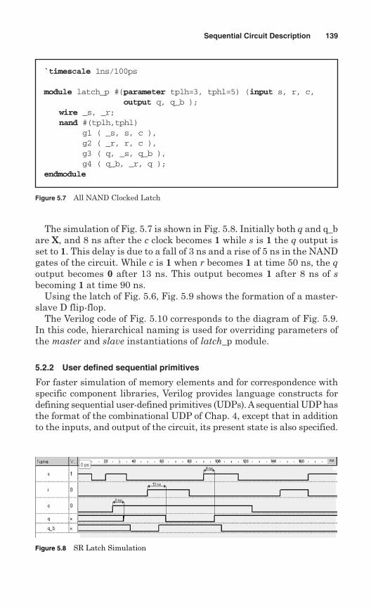
The simulation of Fig. 5.7 is shown in Fig. 5.8. Initially both q and q_bare X, and 8 ns after the c clock becomes 1 while s is 1 the q output isset to 1. This delay is due to a fall of 3 ns and a rise of 5 ns in the NANDgates of the circuit. While c is 1 when r becomes 1 at time 50 ns, the qoutput becomes 0 after 13 ns. This output becomes 1 after 8 ns of sbecoming 1 at time 90 ns.
Using the latch of Fig. 5.6, Fig. 5.9 shows the formation of a master-slave D flip-flop.
The Verilog code of Fig. 5.10 corresponds to the diagram of Fig. 5.9.In this code, hierarchical naming is used for overriding parameters ofthe master and slave instantiations of latch_p module.
5.2.2 User defined sequential primitives
For faster simulation of memory elements and for correspondence withspecific component libraries, Verilog provides language constructs fordefining sequential user-defined primitives (UDPs). Asequential UDP hasthe format of the combinational UDP of Chap. 4, except that in additionto the inputs, and output of the circuit, its present state is also specified.
Sequential Circuit Description 139
`timescale 1ns/100ps
module latch_p #(parameter tplh=3, tphl=5) (input s, r, c,output q, q_b );
wire _s, _r;nand #(tplh,tphl)
g1 ( _s, s, c ),g2 ( _r, r, c ),g3 ( q, _s, q_b ),g4 ( q_b, _r, q );
endmodule
Figure 5.7 All NAND Clocked Latch
Figure 5.8 SR Latch Simulation
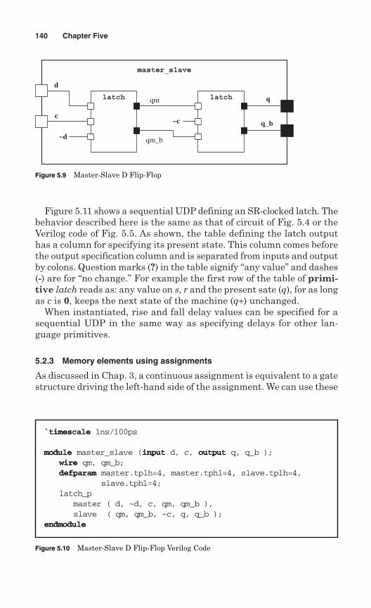
Figure 5.11 shows a sequential UDP defining an SR-clocked latch. Thebehavior described here is the same as that of circuit of Fig. 5.4 or theVerilog code of Fig. 5.5. As shown, the table defining the latch outputhas a column for specifying its present state. This column comes beforethe output specification column and is separated from inputs and outputby colons. Question marks (?) in the table signify “any value” and dashes(-) are for “no change.” For example the first row of the table of primi-tive latch reads as: any value on s, r and the present sate (q), for as longas c is 0, keeps the next state of the machine (q+) unchanged.
When instantiated, rise and fall delay values can be specified for asequential UDP in the same way as specifying delays for other lan-guage primitives.
5.2.3 Memory elements using assignments
As discussed in Chap. 3, a continuous assignment is equivalent to a gatestructure driving the left-hand side of the assignment. We can use these
140 Chapter Five
latch
d
c~c
qm
qm_b~d
master_slave
q
q_b
latch
Figure 5.9 Master-Slave D Flip-Flop
`timescale 1ns/100ps
module master_slave (input d, c, output q, q_b );wire qm, qm_b;defparam master.tplh=4, master.tphl=4, slave.tplh=4,
slave.tphl=4;latch_p
master ( d, ~d, c, qm, qm_b ),slave ( qm, qm_b, ~c, q, q_b );
endmodule
Figure 5.10 Master-Slave D Flip-Flop Verilog Code
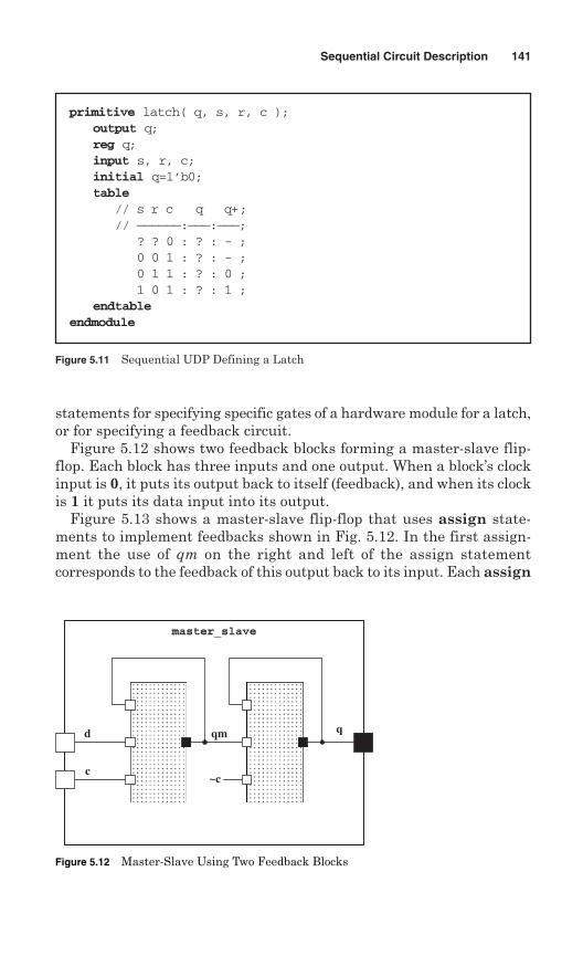
statements for specifying specific gates of a hardware module for a latch,or for specifying a feedback circuit.
Figure 5.12 shows two feedback blocks forming a master-slave flip-flop. Each block has three inputs and one output. When a block’s clockinput is 0, it puts its output back to itself (feedback), and when its clockis 1 it puts its data input into its output.
Figure 5.13 shows a master-slave flip-flop that uses assign state-ments to implement feedbacks shown in Fig. 5.12. In the first assign-ment the use of qm on the right and left of the assign statementcorresponds to the feedback of this output back to its input. Each assign
Sequential Circuit Description 141
primitive latch( q, s, r, c );output q;reg q;input s, r, c;initial q=1’b0;table
// s r c q q+;// ——————:———:———;
? ? 0 : ? : - ;0 0 1 : ? : - ;0 1 1 : ? : 0 ;1 0 1 : ? : 1 ;
endtableendmodule
Figure 5.11 Sequential UDP Defining a Latch
d
c
qm
master_slave
q
~c
Figure 5.12 Master-Slave Using Two Feedback Blocks
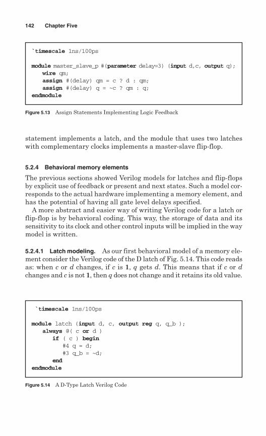
statement implements a latch, and the module that uses two latcheswith complementary clocks implements a master-slave flip-flop.
5.2.4 Behavioral memory elements
The previous sections showed Verilog models for latches and flip-flopsby explicit use of feedback or present and next states. Such a model cor-responds to the actual hardware implementing a memory element, andhas the potential of having all gate level delays specified.
A more abstract and easier way of writing Verilog code for a latch orflip-flop is by behavioral coding. This way, the storage of data and itssensitivity to its clock and other control inputs will be implied in the waymodel is written.
5.2.4.1 Latch modeling. As our first behavioral model of a memory ele-ment consider the Verilog code of the D latch of Fig. 5.14. This code readsas: when c or d changes, if c is 1, q gets d. This means that if c or dchanges and c is not 1, then q does not change and it retains its old value.
142 Chapter Five
`timescale 1ns/100ps
module master_slave_p #(parameter delay=3) (input d,c, output q);wire qm;assign #(delay) qm = c ? d : qm;assign #(delay) q = ~c ? qm : q;
endmodule
Figure 5.13 Assign Statements Implementing Logic Feedback
`timescale 1ns/100ps
module latch (input d, c, output reg q, q_b );always @( c or d )
if ( c ) begin#4 q = d;#3 q_b = ~d;
endendmodule
Figure 5.14 A D-Type Latch Verilog Code
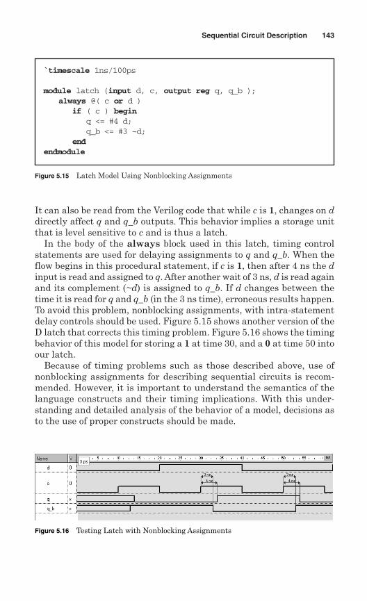
It can also be read from the Verilog code that while c is 1, changes on ddirectly affect q and q_b outputs. This behavior implies a storage unitthat is level sensitive to c and is thus a latch.
In the body of the always block used in this latch, timing controlstatements are used for delaying assignments to q and q_b. When theflow begins in this procedural statement, if c is 1, then after 4 ns the dinput is read and assigned to q. After another wait of 3 ns, d is read againand its complement (~d) is assigned to q_b. If d changes between thetime it is read for q and q_b (in the 3 ns time), erroneous results happen.To avoid this problem, nonblocking assignments, with intra-statementdelay controls should be used. Figure 5.15 shows another version of theD latch that corrects this timing problem. Figure 5.16 shows the timingbehavior of this model for storing a 1 at time 30, and a 0 at time 50 intoour latch.
Because of timing problems such as those described above, use ofnonblocking assignments for describing sequential circuits is recom-mended. However, it is important to understand the semantics of thelanguage constructs and their timing implications. With this under-standing and detailed analysis of the behavior of a model, decisions asto the use of proper constructs should be made.
Sequential Circuit Description 143
`timescale 1ns/100ps
module latch (input d, c, output reg q, q_b );always @( c or d )
if ( c ) beginq <= #4 d;q_b <= #3 ~d;
endendmodule
Figure 5.15 Latch Model Using Nonblocking Assignments
Figure 5.16 Testing Latch with Nonblocking Assignments
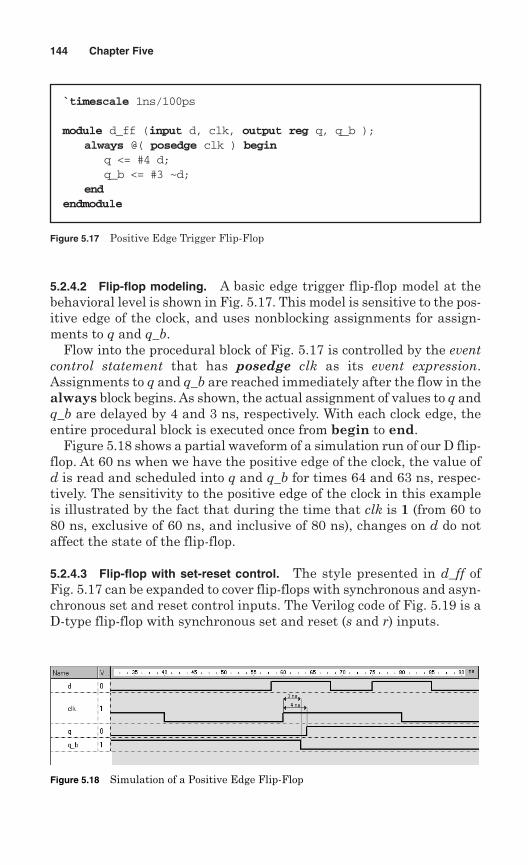
5.2.4.2 Flip-flop modeling. A basic edge trigger flip-flop model at thebehavioral level is shown in Fig. 5.17. This model is sensitive to the pos-itive edge of the clock, and uses nonblocking assignments for assign-ments to q and q_b.
Flow into the procedural block of Fig. 5.17 is controlled by the eventcontrol statement that has posedge clk as its event expression.Assignments to q and q_b are reached immediately after the flow in thealways block begins. As shown, the actual assignment of values to q andq_b are delayed by 4 and 3 ns, respectively. With each clock edge, theentire procedural block is executed once from begin to end.
Figure 5.18 shows a partial waveform of a simulation run of our D flip-flop. At 60 ns when we have the positive edge of the clock, the value ofd is read and scheduled into q and q_b for times 64 and 63 ns, respec-tively. The sensitivity to the positive edge of the clock in this exampleis illustrated by the fact that during the time that clk is 1 (from 60 to80 ns, exclusive of 60 ns, and inclusive of 80 ns), changes on d do notaffect the state of the flip-flop.
5.2.4.3 Flip-flop with set-reset control. The style presented in d_ff ofFig. 5.17 can be expanded to cover flip-flops with synchronous and asyn-chronous set and reset control inputs. The Verilog code of Fig. 5.19 is aD-type flip-flop with synchronous set and reset (s and r) inputs.
144 Chapter Five
`timescale 1ns/100ps
module d_ff (input d, clk, output reg q, q_b );always @( posedge clk ) begin
q <= #4 d;q_b <= #3 ~d;
endendmodule
Figure 5.17 Positive Edge Trigger Flip-Flop
Figure 5.18 Simulation of a Positive Edge Flip-Flop
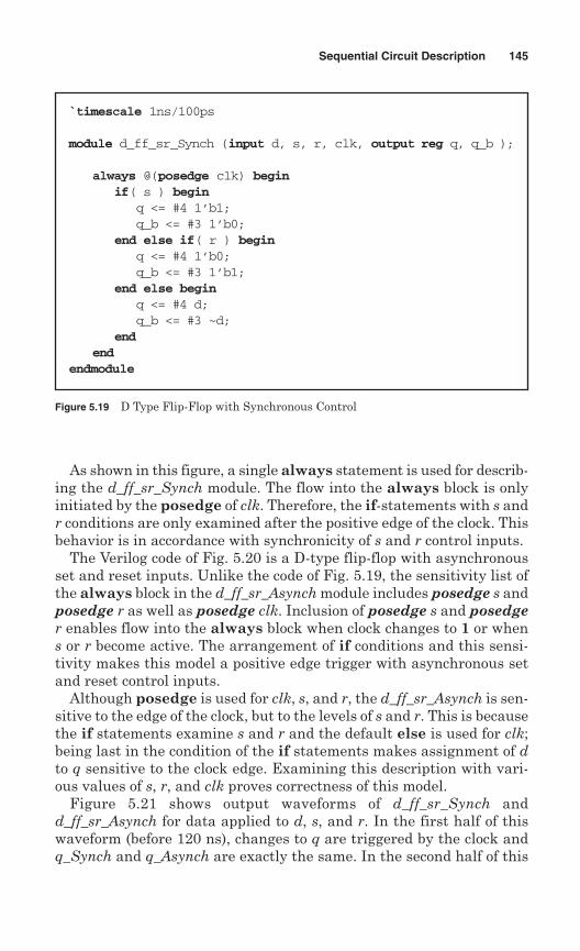
As shown in this figure, a single always statement is used for describ-ing the d_ff_sr_Synch module. The flow into the always block is onlyinitiated by the posedge of clk. Therefore, the if-statements with s andr conditions are only examined after the positive edge of the clock. Thisbehavior is in accordance with synchronicity of s and r control inputs.
The Verilog code of Fig. 5.20 is a D-type flip-flop with asynchronousset and reset inputs. Unlike the code of Fig. 5.19, the sensitivity list ofthe always block in the d_ff_sr_Asynch module includes posedge s andposedge r as well as posedge clk. Inclusion of posedge s and posedger enables flow into the always block when clock changes to 1 or whens or r become active. The arrangement of if conditions and this sensi-tivity makes this model a positive edge trigger with asynchronous setand reset control inputs.
Although posedge is used for clk, s, and r, the d_ff_sr_Asynch is sen-sitive to the edge of the clock, but to the levels of s and r. This is becausethe if statements examine s and r and the default else is used for clk;being last in the condition of the if statements makes assignment of dto q sensitive to the clock edge. Examining this description with vari-ous values of s, r, and clk proves correctness of this model.
Figure 5.21 shows output waveforms of d_ff_sr_Synch andd_ff_sr_Asynch for data applied to d, s, and r. In the first half of thiswaveform (before 120 ns), changes to q are triggered by the clock andq_Synch and q_Asynch are exactly the same. In the second half of this
Sequential Circuit Description 145
`timescale 1ns/100ps
module d_ff_sr_Synch (input d, s, r, clk, output reg q, q_b );
always @(posedge clk) beginif( s ) begin
q <= #4 1’b1;q_b <= #3 1’b0;
end else if( r ) beginq <= #4 1’b0;q_b <= #3 1’b1;
end else beginq <= #4 d;q_b <= #3 ~d;
endend
endmodule
Figure 5.19 D Type Flip-Flop with Synchronous Control
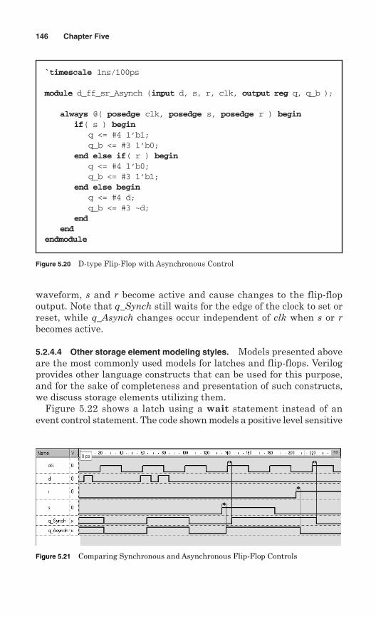
waveform, s and r become active and cause changes to the flip-flopoutput. Note that q_Synch still waits for the edge of the clock to set orreset, while q_Asynch changes occur independent of clk when s or rbecomes active.
5.2.4.4 Other storage element modeling styles. Models presented aboveare the most commonly used models for latches and flip-flops. Verilogprovides other language constructs that can be used for this purpose,and for the sake of completeness and presentation of such constructs,we discuss storage elements utilizing them.
Figure 5.22 shows a latch using a wait statement instead of anevent control statement. The code shown models a positive level sensitive
146 Chapter Five
`timescale 1ns/100ps
module d_ff_sr_Asynch (input d, s, r, clk, output reg q, q_b );
always @( posedge clk, posedge s, posedge r ) beginif( s ) begin
q <= #4 1’b1;q_b <= #3 1’b0;
end else if( r ) beginq <= #4 1’b0;q_b <= #3 1’b1;
end else beginq <= #4 d;q_b <= #3 ~d;
endend
endmodule
Figure 5.20 D-type Flip-Flop with Asynchronous Control
Figure 5.21 Comparing Synchronous and Asynchronous Flip-Flop Controls
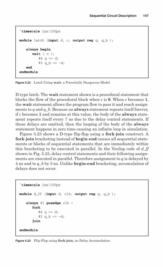
D-type latch. The wait statement shown is a procedural statement thatblocks the flow of the procedural block when c is 0. When c becomes 1,the wait statement allows the program flow to pass it and reach assign-ments to q and q_b. Because an always statement repeats itself forever,if c becomes 1 and remains at this value, the body of the always state-ment repeats itself every 7 ns due to the delay control statements. Ifthese delays are omitted, then the looping of the body of the alwaysstatement happens in zero time causing an infinite loop in simulation.
Figure 5.23 shows a D-type flip-flop using a fork-join construct. Afork-join bracketing instead of begin-end causes all sequential state-ments or blocks of sequential statements that are immediately withinthis bracketing to be executed in parallel. In the Verilog code of d_ffshown in Fig. 5.23, delay control statements and their following assign-ments are executed in parallel. Therefore assignment to q is delayed by4 ns and to q_b by 3 ns. Unlike begin-end bracketing, accumulation ofdelays does not occur.
Sequential Circuit Description 147
`timescale 1ns/100ps
module latch (input d, c, output reg q, q_b );
always beginwait ( c );
#4 q <= d;#3 q_b <= ~d;
endendmodule
Figure 5.22 Latch Using wait, a Potentially Dangerous Model
`timescale 1ns/100ps
module d_ff (input d, clk, output reg q, q_b );
always @( posedge clk )fork
#4 q <= d;#3 q_b <= ~d;
join
endmodule
Figure 5.23 Flip-Flop using fork-join, no Delay Accumulation
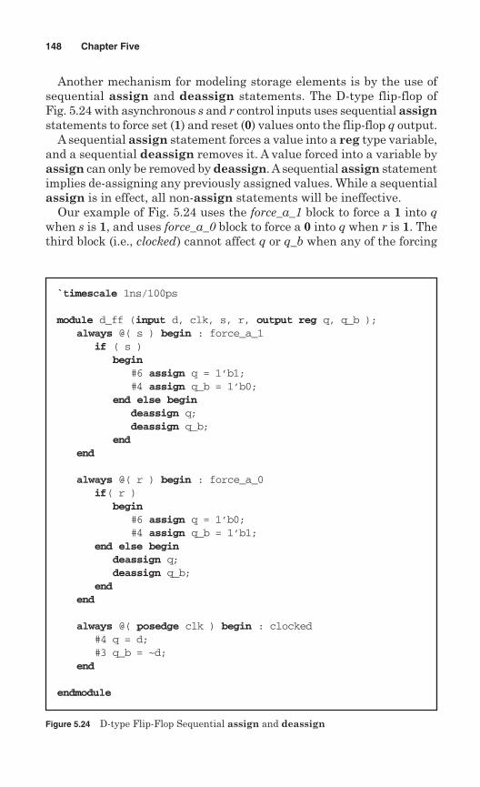
Another mechanism for modeling storage elements is by the use ofsequential assign and deassign statements. The D-type flip-flop ofFig. 5.24 with asynchronous s and r control inputs uses sequential assignstatements to force set (1) and reset (0) values onto the flip-flop q output.
A sequential assign statement forces a value into a reg type variable,and a sequential deassign removes it. A value forced into a variable byassign can only be removed by deassign. A sequential assign statementimplies de-assigning any previously assigned values. While a sequentialassign is in effect, all non-assign statements will be ineffective.
Our example of Fig. 5.24 uses the force_a_1 block to force a 1 into qwhen s is 1, and uses force_a_0 block to force a 0 into q when r is 1. Thethird block (i.e., clocked) cannot affect q or q_b when any of the forcing
148 Chapter Five
`timescale 1ns/100ps
module d_ff (input d, clk, s, r, output reg q, q_b );always @( s ) begin : force_a_1
if ( s )begin
#6 assign q = 1’b1;#4 assign q_b = 1’b0;
end else begindeassign q;deassign q_b;
endend
always @( r ) begin : force_a_0if( r )
begin#6 assign q = 1’b0;#4 assign q_b = 1’b1;
end else begindeassign q;deassign q_b;
endend
always @( posedge clk ) begin : clocked#4 q = d;#3 q_b = ~d;
end
endmodule
Figure 5.24 D-type Flip-Flop Sequential assign and deassign
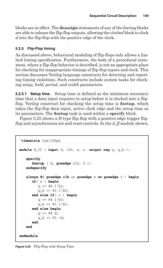
blocks are in effect. The deassign statements of any of the forcing blocksare able to release the flip-flop outputs, allowing the clocked block to clockd into the flip-flop with the positive edge of the clock.
5.2.5 Flip-Flop timing
As discussed above, behavioral modeling of flip-flops only allows a lim-ited timing specification. Furthermore, the body of a procedural state-ment, where a flip-flop behavior is described, is not an appropriate placefor checking for inappropriate timings of flip-flop inputs and clock. Thissection discusses Verilog language constructs for detecting and report-ing timing violations. Such constructs include system tasks for check-ing setup, hold, period, and width parameters.
5.2.5.1 Setup time. Setup time is defined as the minimum necessarytime that a data input requires to setup before it is clocked into a flip-flop. Verilog construct for checking the setup time is $setup, whichtakes the flip-flop data input, active clock edge and the setup time asits parameters. The $setup task is used within a specify block.
Figure 5.25 shows a D-type flip-flop with a positive edge trigger flip-flop and asynchronous set and reset controls. In the d_ff module shown,
Sequential Circuit Description 149
`timescale 1ns/100ps
module d_ff ( input d, clk, s, r, output reg q, q_b );
specify$setup ( d, posedge clk, 5 );
endspecify
always @( posedge clk or posedge s or posedge r ) beginif( s ) begin
q <= #4 1’b1;q_b <= #3 1’b0;
end else if( r ) beginq <= #4 1’b0;q_b <= #3 1’b1;
end else beginq <= #4 d;q_b <= #3 ~d;
endend
endmodule
Figure 5.25 Flip-Flop with Setup Time
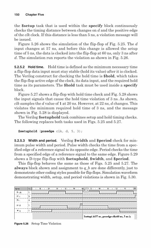
the $setup task that is used within the specify block continuouslychecks the timing distance between changes on d and the positive edgeof the clk clock. If this distance is less than 5 ns, a violation message willbe issued.
Figure 5.26 shows the simulation of the flip-flop of Fig. 5.25. The dinput changes at 57 ns, and before this change is allowed the setuptime of 5 ns, the data is clocked into the flip-flop at 60 ns, only 3 ns afterd. The simulation run reports the violation as shown in Fig. 5.26.
5.2.5.2 Hold time. Hold time is defined as the minimum necessary timea flip-flop data input must stay stable (hold its value) after it is clocked.The Verilog construct for checking the hold time is $hold, which takesthe flip-flop active edge of the clock, its data input, and the required holdtime as its parameters. The $hold task must be used inside a specifyblock.
Figure 5.27 shows a flip-flop with hold time check and Fig. 5.28 showsthe input signals that cause the hold time violation of 3 ns. As shown,clk samples the d value of 1 at 20 ns. However, at 22 ns, d changes. Thisviolates the minimum required hold time of 3 ns, and the messageshown in Fig. 5.28 is displayed.
The Verilog $setuphold task combines setup and hold timing checks.The following replaces both tasks used in Figs. 5.25 and 5.27.
$setuphold (posedge clk, d, 5, 3);
5.2.5.3 Width and period. Verilog $width and $period check for min-imum pulse width and period. Pulse width checks the time from a spec-ified edge of a reference signal to its opposite edge. Period checks the timefrom a specified edge of a reference signal to the same edge. Figure 5.29shows a D-type flip-flop with $setuphold, $width, and $period.
This flip-flop behaves the same as those of Figs. 5.25 and 5.27. Thealways block shown and assignment to q_b are done differently, just todemonstrate other coding styles possible for flip-flops. Simulation waveformdemonstrating width, setup, and period violations is shown in Fig. 5.30.
150 Chapter Five
Figure 5.26 Setup Time Violation
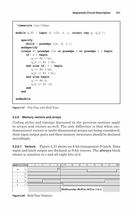
5.2.6 Memory vectors and arrays
Coding styles and timings discussed in the previous sections applyto arrays and vectors as well. The only difference is that when one-dimensional vectors or multi-dimensional arrays are being considered,their input output ports and their memory structures should be declaredaccordingly.
5.2.6.1 Vectors. Figure 5.31 shows an 8-bit transparent D-latch. Datainput and latch output are declared as 8-bit vercors. The always blockshown is sensitive to c and all eight bits of d.
Sequential Circuit Description 151
`timescale 1ns/100ps
module d_ff ( input d, clk, s, r, output reg q, q_b );
specify$hold ( posedge clk, d, 3 );
endspecifyalways @( posedge clk or posedge s or posedge r ) begin
if( s ) beginq <= #4 1’b1;q_b <= #3 1’b0;
end else if( r ) beginq <= #4 1’b0;q_b <= #3 1’b1;
end else beginq <= #4 d;q_b <= #3 ~d;
endend
endmodule
Figure 5.27 Flip-Flop with Hold Time
Figure 5.28 Hold Time Violation
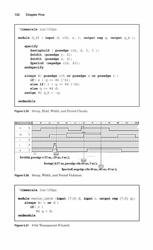
152 Chapter Five
`timescale 1ns/100ps
module d_ff ( input d, clk, s, r, output reg q, output q_b );
specify$setuphold ( posedge clk, d, 5, 3 );$width (posedge r, 4);$width (posedge s, 4);$period (negedge clk, 43);
endspecify
always @( posedge clk or posedge s or posedge r )if( s ) q <= #4 1’b1;else if( r ) q <= #4 1’b0;else q <= #4 d;
assign #2 q_b = ~q;
endmodule
Figure 5.29 Setup, Hold, Width, and Period Checks
Figure 5.30 Setup, Width, and Period Violation
`timescale 1ns/100ps
module vector_latch (input [7:0] d, input c, output reg [7:0] q);always @( c or d )
if( c )#4 q = d;
endmodule
Figure 5.31 8-bit Transparent D-Latch
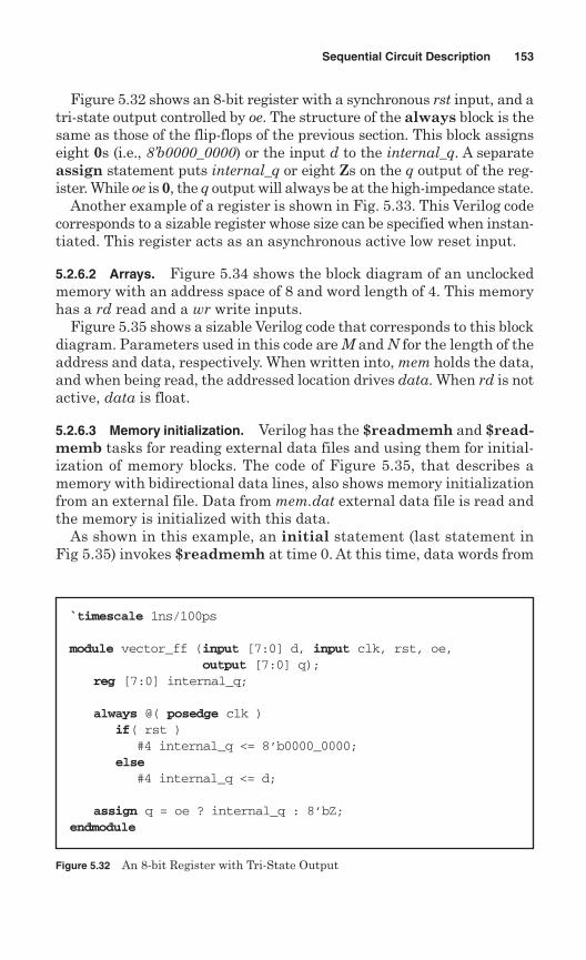
Figure 5.32 shows an 8-bit register with a synchronous rst input, and atri-state output controlled by oe. The structure of the always block is thesame as those of the flip-flops of the previous section. This block assignseight 0s (i.e., 8’b0000_0000) or the input d to the internal_q. A separateassign statement puts internal_q or eight Zs on the q output of the reg-ister. While oe is 0, the q output will always be at the high-impedance state.
Another example of a register is shown in Fig. 5.33. This Verilog codecorresponds to a sizable register whose size can be specified when instan-tiated. This register acts as an asynchronous active low reset input.
5.2.6.2 Arrays. Figure 5.34 shows the block diagram of an unclockedmemory with an address space of 8 and word length of 4. This memoryhas a rd read and a wr write inputs.
Figure 5.35 shows a sizable Verilog code that corresponds to this blockdiagram. Parameters used in this code are M and N for the length of theaddress and data, respectively. When written into, mem holds the data,and when being read, the addressed location drives data. When rd is notactive, data is float.
5.2.6.3 Memory initialization. Verilog has the $readmemh and $read-memb tasks for reading external data files and using them for initial-ization of memory blocks. The code of Figure 5.35, that describes amemory with bidirectional data lines, also shows memory initializationfrom an external file. Data from mem.dat external data file is read andthe memory is initialized with this data.
As shown in this example, an initial statement (last statement inFig 5.35) invokes $readmemh at time 0. At this time, data words from
Sequential Circuit Description 153
`timescale 1ns/100ps
module vector_ff (input [7:0] d, input clk, rst, oe, output [7:0] q);
reg [7:0] internal_q;
always @( posedge clk )if( rst )
#4 internal_q <= 8’b0000_0000;else
#4 internal_q <= d;
assign q = oe ? internal_q : 8’bZ;endmodule
Figure 5.32 An 8-bit Register with Tri-State Output
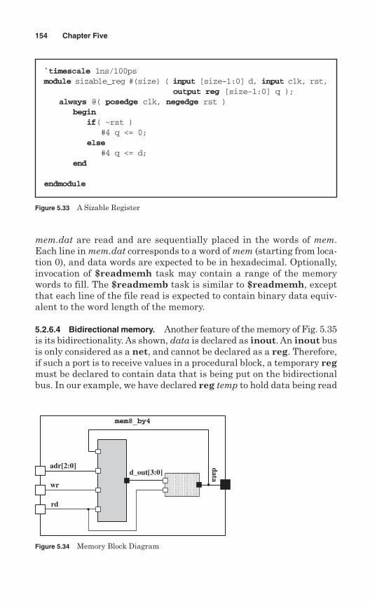
mem.dat are read and are sequentially placed in the words of mem.Each line in mem.dat corresponds to a word of mem (starting from loca-tion 0), and data words are expected to be in hexadecimal. Optionally,invocation of $readmemh task may contain a range of the memorywords to fill. The $readmemb task is similar to $readmemh, exceptthat each line of the file read is expected to contain binary data equiv-alent to the word length of the memory.
5.2.6.4 Bidirectional memory. Another feature of the memory of Fig. 5.35is its bidirectionality. As shown, data is declared as inout. An inout busis only considered as a net, and cannot be declared as a reg. Therefore,if such a port is to receive values in a procedural block, a temporary regmust be declared to contain data that is being put on the bidirectionalbus. In our example, we have declared reg temp to hold data being read
154 Chapter Five
`timescale 1ns/100psmodule sizable_reg #(size) ( input [size-1:0] d, input clk, rst,
output reg [size-1:0] q );always @( posedge clk, negedge rst )
beginif( ~rst )
#4 q <= 0;else
#4 q <= d;end
endmodule
Figure 5.33 A Sizable Register
Figure 5.34 Memory Block Diagram
data
adr[2:0]
mem8_by4
d_out[3:0]
wr
rd
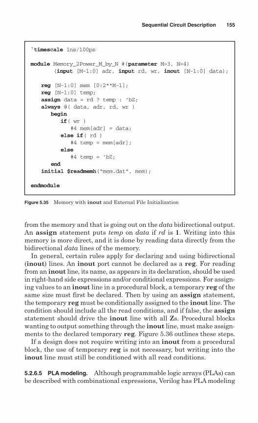
from the memory and that is going out on the data bidirectional output.An assign statement puts temp on data if rd is 1. Writing into thismemory is more direct, and it is done by reading data directly from thebidirectional data lines of the memory.
In general, certain rules apply for declaring and using bidirectional(inout) lines. An inout port cannot be declared as a reg. For readingfrom an inout line, its name, as appears in its declaration, should be usedin right-hand side expressions and/or conditional expressions. For assign-ing values to an inout line in a procedural block, a temporary reg of thesame size must first be declared. Then by using an assign statement,the temporary reg must be conditionally assigned to the inout line. Thecondition should include all the read conditions, and if false, the assignstatement should drive the inout line with all Zs. Procedural blockswanting to output something through the inout line, must make assign-ments to the declared temporary reg. Figure 5.36 outlines these steps.
If a design does not require writing into an inout from a proceduralblock, the use of temporary reg is not necessary, but writing into theinout line must still be conditioned with all read conditions.
5.2.6.5 PLA modeling. Although programmable logic arrays (PLAs) canbe described with combinational expressions, Verilog has PLA modeling
Sequential Circuit Description 155
`timescale 1ns/100ps
module Memory_2Power_M_by_N #(parameter M=3, N=4) (input [M-1:0] adr, input rd, wr, inout [N-1:0] data);
reg [N-1:0] mem [0:2**M-1];reg [N-1:0] temp;assign data = rd ? temp : ‘bZ;always @( data, adr, rd, wr )
beginif( wr )
#4 mem[adr] = data;else if( rd )
#4 temp = mem[adr];else
#4 temp = ‘bZ;end
initial $readmemh(“mem.dat”, mem);
endmodule
Figure 5.35 Memory with inout and External File Initialization
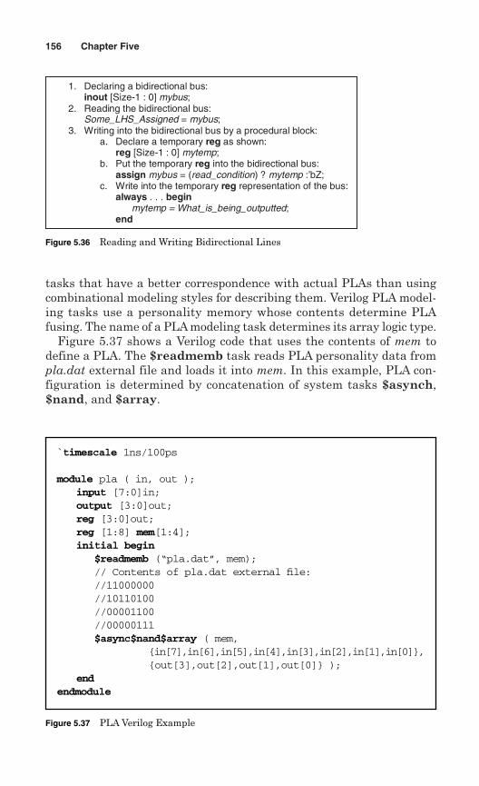
tasks that have a better correspondence with actual PLAs than usingcombinational modeling styles for describing them. Verilog PLA model-ing tasks use a personality memory whose contents determine PLAfusing. The name of a PLA modeling task determines its array logic type.
Figure 5.37 shows a Verilog code that uses the contents of mem todefine a PLA. The $readmemb task reads PLA personality data frompla.dat external file and loads it into mem. In this example, PLA con-figuration is determined by concatenation of system tasks $asynch,$nand, and $array.
156 Chapter Five
1. Declaring a bidirectional bus:inout [Size-1 : 0] mybus;
2. Reading the bidirectional bus:Some_LHS_Assigned = mybus;
3. Writing into the bidirectional bus by a procedural block:a. Declare a temporary reg as shown:
reg [Size-1 : 0] mytemp;b. Put the temporary reg into the bidirectional bus:
assign mybus = (read_condition) ? mytemp :’bZ;c. Write into the temporary reg representation of the bus:
always . . . beginmytemp = What_is_being_outputted;
end
Figure 5.36 Reading and Writing Bidirectional Lines
`timescale 1ns/100ps
module pla ( in, out );input [7:0]in;output [3:0]out;reg [3:0]out;reg [1:8] mem[1:4];initial begin
$readmemb (“pla.dat”, mem);// Contents of pla.dat external file://11000000//10110100//00001100//00000111$async$nand$array ( mem,
{in[7],in[6],in[5],in[4],in[3],in[2],in[1],in[0]},{out[3],out[2],out[1],out[0]} );
endendmodule
Figure 5.37 PLA Verilog Example
A PLA task uses a task name that is a concatenation of the PLA type,its logic and its format. The arguments of a PLA task are the personal-ization memory, the input terms, and the output terms. Input and outputterms must be concatenation of scalars, concatenated to form the size,the memory word-size, and the number of words respectively. The outputterms must be declared as reg.
The type of a PLA can be synchronous or asynchronous ($synch or$asynch). The PLA logic is determined by its logic specification that canbe $and, $or, $nand, or $nor. For a PLA with the $nand logic and$array format, each of its outputs is bit-by-bit NAND result of thoseinput bits that have a corresponding 1 in the PLA personality data. Withpla.dat contents as shown in comments of the Verilog code of Fig. 5.37,this PLA generates the following expressions on its outputs.
out3 = nand(in7, in6);out2 = nand(in7, in5, in4, in2);out1 = nand(in3, in2);out0 = nand(in2, in1, in0);
5.3 Functional Registers
A register is defined as a group of flip-flops with a common clock. Theterm register also applies to a group of latches, but to differentiate themwe will be very precise in using the correct terminology. We will referto a group of latches by its size, e.g., octal latch, or nibble latch. We definea functional register as a group of flip-flops with a common clock andwith some functionality, such as counting and shifting. Styles used forVerilog coding of functional registers are similar to those of flip-flops andregisters described in the previous section. The difference is the addedarithmetic or logical functionality to the code of functional registers.
5.3.1 Shift registers
Coding shift registers in Verilog is very similar to registers of the previ-ous section. The addition of shift operations to these styles will be discussedhere. Several shift register examples in this section take advantage ofshift operators and concatenation.
5.3.1.1 Basic shifter. Shown in Fig. 5.38 is a 4-bit shift register withload, reset, and shift capabilities. The l_r input controls left or right shift-ing. In either case, the vacated bit will be filled with the contents of s_inserial input.
Verilog code of Fig. 5.39 corresponds to this shift register. As shown,all shift register operations are synchronized with the positive edge ofthe circuit clock. The active high rst input causes 4'b0000 to be loadedinto the q output. The ld input performs parallel loading of d into q. If
Sequential Circuit Description 157
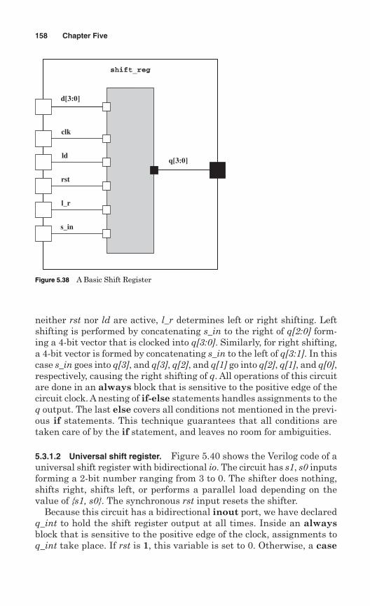
neither rst nor ld are active, l_r determines left or right shifting. Leftshifting is performed by concatenating s_in to the right of q[2:0] form-ing a 4-bit vector that is clocked into q[3:0]. Similarly, for right shifting,a 4-bit vector is formed by concatenating s_in to the left of q[3:1]. In thiscase s_in goes into q[3], and q[3], q[2], and q[1] go into q[2], q[1], and q[0],respectively, causing the right shifting of q. All operations of this circuitare done in an always block that is sensitive to the positive edge of thecircuit clock. A nesting of if-else statements handles assignments to theq output. The last else covers all conditions not mentioned in the previ-ous if statements. This technique guarantees that all conditions aretaken care of by the if statement, and leaves no room for ambiguities.
5.3.1.2 Universal shift register. Figure 5.40 shows the Verilog code of auniversal shift register with bidirectional io. The circuit has s1, s0 inputsforming a 2-bit number ranging from 3 to 0. The shifter does nothing,shifts right, shifts left, or performs a parallel load depending on thevalue of {s1, s0}. The synchronous rst input resets the shifter.
Because this circuit has a bidirectional inout port, we have declaredq_int to hold the shift register output at all times. Inside an alwaysblock that is sensitive to the positive edge of the clock, assignments toq_int take place. If rst is 1, this variable is set to 0. Otherwise, a case
158 Chapter Five
d[3:0]
clk
shift_reg
q[3:0]ld
rst
l_r
s_in
Figure 5.38 A Basic Shift Register
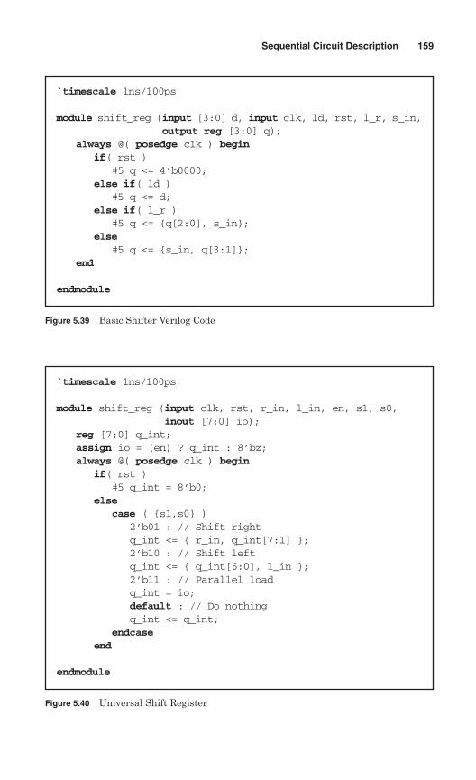
Sequential Circuit Description 159
`timescale 1ns/100ps
module shift_reg (input [3:0] d, input clk, ld, rst, l_r, s_in,output reg [3:0] q);
always @( posedge clk ) beginif( rst )
#5 q <= 4’b0000;else if( ld )
#5 q <= d;else if( l_r )
#5 q <= {q[2:0], s_in};else
#5 q <= {s_in, q[3:1]};end
endmodule
Figure 5.39 Basic Shifter Verilog Code
`timescale 1ns/100ps
module shift_reg (input clk, rst, r_in, l_in, en, s1, s0,inout [7:0] io);
reg [7:0] q_int;assign io = (en) ? q_int : 8’bz;always @( posedge clk ) begin
if( rst )#5 q_int = 8’b0;
elsecase ( {s1,s0} )
2’b01 : // Shift rightq_int <= { r_in, q_int[7:1] };2’b10 : // Shift leftq_int <= { q_int[6:0], l_in };2’b11 : // Parallel load q_int = io;default : // Do nothingq_int <= q_int;
endcaseend
endmodule
Figure 5.40 Universal Shift Register
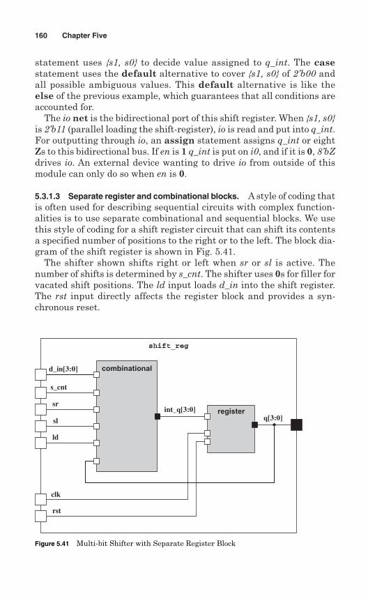
statement uses {s1, s0} to decide value assigned to q_int. The casestatement uses the default alternative to cover {s1, s0} of 2’b00 andall possible ambiguous values. This default alternative is like theelse of the previous example, which guarantees that all conditions areaccounted for.
The io net is the bidirectional port of this shift register. When {s1, s0}is 2’b11 (parallel loading the shift-register), io is read and put into q_int.For outputting through io, an assign statement assigns q_int or eightZs to this bidirectional bus. If en is 1 q_int is put on i0, and if it is 0, 8’bZdrives io. An external device wanting to drive io from outside of thismodule can only do so when en is 0.
5.3.1.3 Separate register and combinational blocks. A style of coding thatis often used for describing sequential circuits with complex function-alities is to use separate combinational and sequential blocks. We usethis style of coding for a shift register circuit that can shift its contentsa specified number of positions to the right or to the left. The block dia-gram of the shift register is shown in Fig. 5.41.
The shifter shown shifts right or left when sr or sl is active. Thenumber of shifts is determined by s_cnt. The shifter uses 0s for filler forvacated shift positions. The ld input loads d_in into the shift register.The rst input directly affects the register block and provides a syn-chronous reset.
160 Chapter Five
d_in[3:0]
s_cnt
shift_reg
sr
sl
ld
combinational
clk
int_q[3:0]q[3:0]
rst
register
Figure 5.41 Multi-bit Shifter with Separate Register Block
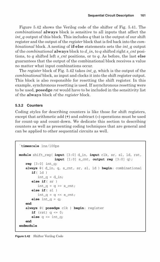
Figure 5.42 shows the Verilog code of the shifter of Fig. 5.41. Thecombinational always block is sensitive to all inputs that affect theint_q output of this block. This includes q that is the output of our shiftregister and the output of the register block that is fed back into the com-binational block. A nesting of if-else statements sets the int_q outputof the combinational always block to d_in, to q shifted right s_cnt posi-tions, to q shifted left s_cnt positions, or to q. As before, the last elseguarantees that the output of the combinational block receives a valueno matter what input combinations occur.
The register block of Fig. 5.42 takes int_q, which is the output of thecombinational block, as input and clocks it into the shift register output.This block is also responsible for resetting the shift register. In thisexample, synchronous resetting is used. If asynchronous resetting wereto be used, posedge rst would have to be included in the sensitivity listof the always block of the register block.
5.3.2 Counters
Coding styles for describing counters is like those for shift registers,except that arithmetic add (+) and subtract (--) operations must be usedfor count-up and count-down. We dedicate this section to describingcounters as well as presenting coding techniques that are general andcan be applied to other sequential circuits as well.
Sequential Circuit Description 161
`timescale 1ns/100ps
module shift_reg( input [3:0] d_in, input clk, sr, sl, ld, rst,input [1:0] s_cnt, output reg [3:0] q);
reg [3:0] int_q;always @( d_in, q, s_cnt, sr, sl, ld ) begin: combinational
if( ld )int_q = d_in;
else if( sr )int_q = q >> s_cnt;
else if( sl )int_q = q << s_cnt;
else int_q = q;endalways @( posedge clk ) begin: register
if (rst) q <= 0;else q <= int_q;
endendmodule
Figure 5.42 Shifter Verilog Code
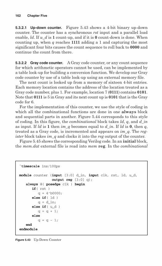
5.3.2.1 Up-down counter. Figure 5.43 shows a 4-bit binary up-downcounter. The counter has a synchronous rst input and a parallel loadenable, ld. If u_d is 1 count-up, and if it is 0 count-down is done. Whencounting up, when q reaches 1111 adding a 1 and capturing the mostsignificant four bits causes the count sequence to roll back to 0000 andcontinue the count from there.
5.3.2.2 Gray code counter. A Gray code counter, or any count sequencefor which arithmetic operators cannot be used, can be implemented bya table look-up for building a conversion function. We develop our Graycode counter by use of a table look-up using an external memory file.
The next count is looked up from a memory of sixteen 4-bit entries.Each memory location contains the address of the location treated as aGray code number, plus 1. For example, location 7 (0111) contains 0101.Note that 0111 is 5 in Gray and its next count up is 0101 that is the Graycode for 6.
For the implementation of this counter, we use the style of coding inwhich all the combinational functions are done in one always blockand sequential parts in another. Figure 5.44 corresponds to this styleof coding. In this figure, the combinational block takes ld, q, and d_inas input. If ld is 1 then im_q becomes equal to d_in. If ld is 0, then q,treated as a Gray code, is incremented and appears on im_q. The reg-ister block takes im_q and clocks it into the reg output of the counter.
Figure 5.45 shows the corresponding Verilog code. In an initial block,the mem.dat external file is read into mem reg. In the combinational
162 Chapter Five
`timescale 1ns/100ps
module counter (input [3:0] d_in, input clk, rst, ld, u_d,output reg [3:0] q);
always @( posedge clk ) beginif( rst )
q = 4’b0000;else if( ld )
q = d_in;else if( u_d )
q = q + 1;else
q = q - 1;end
endmodule
Figure 5.43 Up-Down Counter
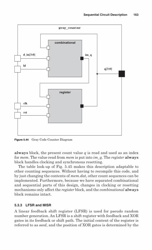
always block, the present count value q is read and used as an indexfor mem. The value read from mem is put into im_q. The register alwaysblock handles clocking and synchronous resetting.
The table look-up of Fig. 5.45 makes this description adaptable toother counting sequences. Without having to recompile this code, andby just changing the contents of mem.dat, other count sequences can beimplemented. Furthermore, because we have separated combinationaland sequential parts of this design, changes in clocking or resettingmechanisms only affect the register block, and the combinational alwaysblock remains intact.
5.3.3 LFSR and MISR
A linear feedback shift register (LFSR) is used for pseudo randomnumber generation. An LFSR is a shift register with feedback and XORgates in its feedback or shift path. The initial content of the register isreferred to as seed, and the position of XOR gates is determined by the
Sequential Circuit Description 163
d_in[3:0]
ld
gray_counter
combinational
clk
im_q
q[3:0]
rst
register
Figure 5.44 Gray Code Counter Diagram
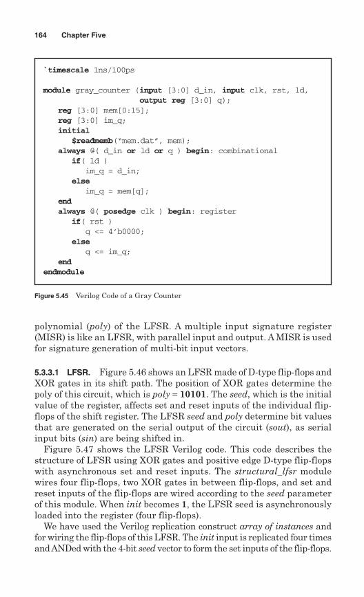
polynomial (poly) of the LFSR. A multiple input signature register(MISR) is like an LFSR, with parallel input and output. A MISR is usedfor signature generation of multi-bit input vectors.
5.3.3.1 LFSR. Figure 5.46 shows an LFSR made of D-type flip-flops andXOR gates in its shift path. The position of XOR gates determine thepoly of this circuit, which is poly = 10101. The seed, which is the initialvalue of the register, affects set and reset inputs of the individual flip-flops of the shift register. The LFSR seed and poly determine bit valuesthat are generated on the serial output of the circuit (sout), as serialinput bits (sin) are being shifted in.
Figure 5.47 shows the LFSR Verilog code. This code describes thestructure of LFSR using XOR gates and positive edge D-type flip-flopswith asynchronous set and reset inputs. The structural_lfsr modulewires four flip-flops, two XOR gates in between flip-flops, and set andreset inputs of the flip-flops are wired according to the seed parameterof this module. When init becomes 1, the LFSR seed is asynchronouslyloaded into the register (four flip-flops).
We have used the Verilog replication construct array of instances andfor wiring the flip-flops of this LFSR. The init input is replicated four timesand ANDed with the 4-bit seed vector to form the set inputs of the flip-flops.
164 Chapter Five
`timescale 1ns/100ps
module gray_counter (input [3:0] d_in, input clk, rst, ld,output reg [3:0] q);
reg [3:0] mem[0:15];reg [3:0] im_q;initial
$readmemb(“mem.dat”, mem);always @( d_in or ld or q ) begin: combinational
if( ld )im_q = d_in;
elseim_q = mem[q];
endalways @( posedge clk ) begin: register
if( rst )q <= 4’b0000;
elseq <= im_q;
endendmodule
Figure 5.45 Verilog Code of a Gray Counter
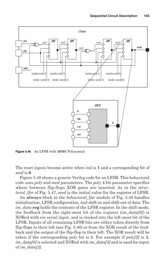
The reset inputs become active when init is 1 and a corresponding bit ofseed is 0.
Figure 5.48 shows a generic Verilog code for an LFSR. This behavioralcode uses poly and seed parameters. The poly 4-bit parameter specifieswhere between flip-flops XOR gates are inserted. As in the struc-tural_lfsr of Fig. 5.47, seed is the initial value for the register of LFSR.
An always block in the behavioral_lfsr module of Fig. 5.48 handlesinitialization, LFSR configuration, and shift-in and shift-out of data. Theim_data reg holds the contents of the LFSR register. In the shift mode,the feedback from the right-most bit of the register (im_data[0]) isXORed with sin serial input, and is clocked into the left-most bit of theLFSR. Inputs of all remaining LFSR bits are either taken directly fromflip-flops to their left (see Fig. 5.46) or from the XOR result of the feed-back and the output of the flip-flop to their left. The XOR result will betaken if the corresponding poly bit is 1. For example if poly[2] is 1,im_data[0] is selected and XORed with im_data[3] and is used for inputof im_data[2].
Sequential Circuit Description 165
dffsin im1 im2
im3
im4 im5
clk
init
init&seed[3]
init&~seed[3]
init&seed[2]
init&~seed[2] init&~seed[1]
init&seed[0]
init&~seed[0]
lfsr
sout
d
clk
dff
q
rst
set
dff dff dff
init&seed[1]
Figure 5.46 An LFSR with 10101 Polynomial
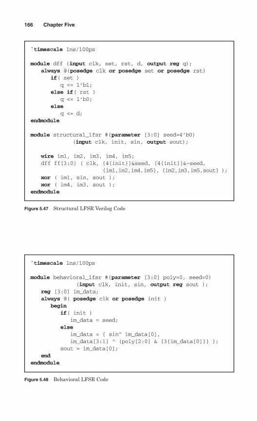
166 Chapter Five
`timescale 1ns/100ps
module dff (input clk, set, rst, d, output reg q);always @(posedge clk or posedge set or posedge rst)
if( set ) q <= 1’b1;
else if( rst ) q <= 1’b0;
elseq <= d;
endmodule
module structural_lfsr #(parameter [3:0] seed=4’b0) (input clk, init, sin, output sout);
wire im1, im2, im3, im4, im5;dff ff[3:0] ( clk, {4{init}}&seed, {4{init}}&~seed,
{im1,im2,im4,im5}, {im2,im3,im5,sout} );xor ( im1, sin, sout );xor ( im4, im3, sout );
endmodule
Figure 5.47 Structural LFSR Verilog Code
`timescale 1ns/100ps
module behavioral_lfsr #(parameter [3:0] poly=0, seed=0) (input clk, init, sin, output reg sout );
reg [3:0] im_data;always @( posedge clk or posedge init )
beginif( init )
im_data = seed;else
im_data = { sin^ im_data[0], im_data[3:1] ^ (poly[2:0] & {3{im_data[0]}} };
sout = im_data[0];end
endmodule
Figure 5.48 Behavioral LFSR Code
5.3.3.2 Multiple input signature register. A MISR is used for signaturegeneration and data compression. Over a period of several clocks, par-allel data into a MISR are compressed with the existing MISR data. Thefinal data depends on the MISR initial data (seed) and its XOR andfeedback structure (poly).
Figure 5.49 shows a MISR with a configurable polynomial (poly). Thecircuit has a reset input that initializes it to 0000. This initial value isconsidered as the seed of this MISR example.
The Verilog code of Fig. 5.50 corresponds to the hardware of Fig. 5.49.An always block in this code handles resetting and signature genera-tion. The generation of the signature is based on the input poly that con-figures the feedback (d_out[0]) connections to the XOR gates that arebetween the flip-flops.
This configuration is done by the expression that appears on the right-hand side of d_out. In this expression parallel data input bits (d_in) areXORed with right shifted output data ({1’b0, d_out[3:1]}), and are thenselectively XORed with feedback coming from the right-most bit of theshift register. Selecting feedback from the right-most bit to affect inputlogic of a register bit is determined by the bits of poly. This selection isdone by ANDing poly bits with the replication of the feedback from theright-most bit.
5.3.4 Stacks and queues
A combination of styles presented for register modeling and memoryread and write operations can be used for describing stacks and queues.A queue has a memory block and read and write pointers. Read andwrite pointers are described as registers and counters that provideaddress pointers for the queue memory. Combinational logic blocks areused for providing full and empty indicators for the queue memory.
5.3.4.1 FIFO queue. A first in first out (FIFO) queue is a queue of datasuch that the data that is written into it first, is read from it first.Figure 5.51 shows the block diagram of a FIFO queue.
The pointer block provides read and write pointers according to readand write operations into the queue. The count block keeps track of thenumber of data in the queue and issues empty and full flags. Theseflags are generated by combinational blocks using the present count ofdata as input. The read block uses the read pointer to read from thequeue memory, and the write block uses the write pointer to write intothis memory. The read and write blocks share the fifo_ram memory.Read and write operations are synchronized with the circuit clock.
The Verilog code of the FIFO queue is shown in Fig. 5.52. As shown, fouralways blocks that are sensitive to the positive edge of the clock handlewriting (write), reading (read), updating read and write pointers (pointer),
Sequential Circuit Description 167
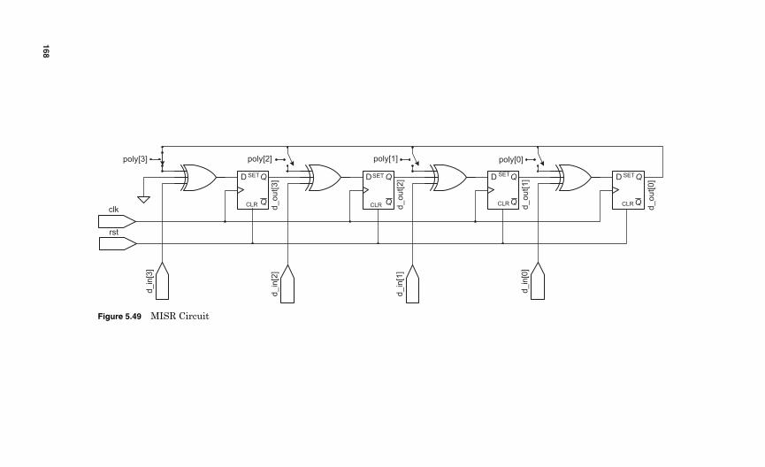
168
Q
QSET
CLR
D
Q
QSET
CLR
D
Q
QSET
CLR
D
Q
QSET
CLR
D
poly[1]poly[2] poly[0]d_in
[3]
d_
in[2
]
d_
in[1
]
d_in
[0]
clk
poly[3]
d_
ou
t[3
]
d_
ou
t[2
]
d_
ou
t[1
]
d_
ou
t[0
]
rst
Figure 5.49 MISR Circuit
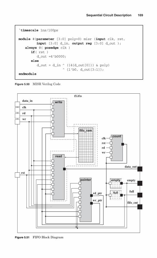
Sequential Circuit Description 169
`timescale 1ns/100ps
module #(parameter [3:0] poly=0) misr (input clk, rst, input [3:0] d_in, output reg [3:0] d_out );
always @( posedge clk )if( rst )
d_out =4’b0000;else
d_out = d_in ^ ({4{d_out[0]}} & poly)^ {1’b0, d_out[3:1]};
endmodule
Figure 5.50 MISR Verilog Code
rd_ptr
wr_ptr
clk
data_in
fifo
rd
wr
write
full
empty
read
data_out
rst
count
fifo_cnt
clk
rst
rd
wr
empty
full
fifo_ram
pointer
Figure 5.51 FIFO Block Diagram
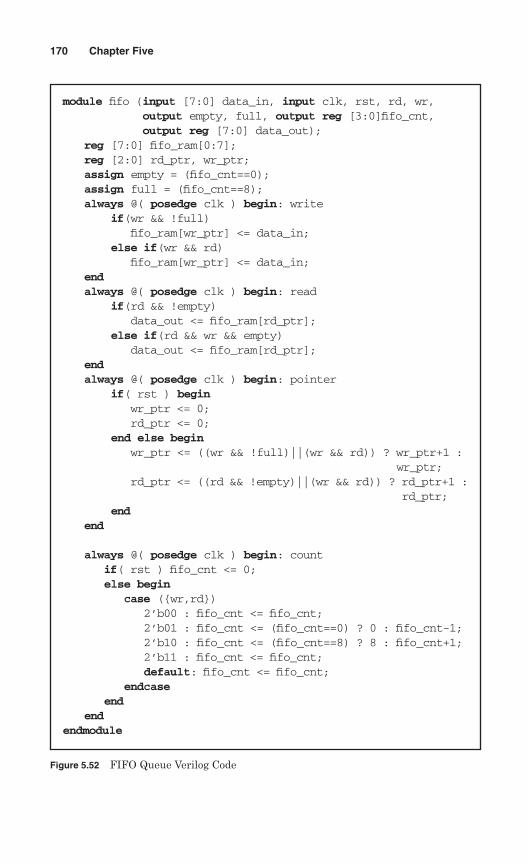
170 Chapter Five
module fifo (input [7:0] data_in, input clk, rst, rd, wr,output empty, full, output reg [3:0]fifo_cnt,output reg [7:0] data_out);
reg [7:0] fifo_ram[0:7];reg [2:0] rd_ptr, wr_ptr;assign empty = (fifo_cnt==0);assign full = (fifo_cnt==8);always @( posedge clk ) begin: write
if(wr && !full) fifo_ram[wr_ptr] <= data_in;
else if(wr && rd)fifo_ram[wr_ptr] <= data_in;
endalways @( posedge clk ) begin: read
if(rd && !empty) data_out <= fifo_ram[rd_ptr];
else if(rd && wr && empty)data_out <= fifo_ram[rd_ptr];
endalways @( posedge clk ) begin: pointer
if( rst ) beginwr_ptr <= 0;rd_ptr <= 0;
end else begin wr_ptr <= ((wr && !full)||(wr && rd)) ? wr_ptr+1 :
wr_ptr;rd_ptr <= ((rd && !empty)||(wr && rd)) ? rd_ptr+1 :
rd_ptr;end
end
always @( posedge clk ) begin: countif( rst ) fifo_cnt <= 0;else begin
case ({wr,rd})2’b00 : fifo_cnt <= fifo_cnt;2’b01 : fifo_cnt <= (fifo_cnt==0) ? 0 : fifo_cnt-1;2’b10 : fifo_cnt <= (fifo_cnt==8) ? 8 : fifo_cnt+1;2’b11 : fifo_cnt <= fifo_cnt;default: fifo_cnt <= fifo_cnt;
endcaseend
endendmodule
Figure 5.52 FIFO Queue Verilog Code
and keeping the FIFO count (count). Concurrent with these blocks twoassign statements issue empty and full.
The write block writes into fifo_ram if it is not full. If both rd and wrinputs are active (reading at the same time as writing), full is notchecked and memory is written into. If none of these conditions hold,then memory is left intact. The read block reads from fifo_ram if it isnot empty. If it is empty and both rd and wr inputs are active, data fromthe present pointer location is read into data_out. This output reg is leftintact if neither read conditions are satisfied.
The pointer block implements two counters for read and write point-ers. Separate from these pointers, the count always block performsincrementing and decrementing fifo_cnt depending on write and readoperations being done. The count block uses a case statement withdefault, which handles ambiguous values on wr and rd. In this case,fifo_cnt is left intact.
5.4 State Machine Coding
Coding styles presented so far can further be generalized to cover finitestate machines of any type. This section shows coding for Moore andMealy state machines. The examples we will use are simple sequencedetectors, yet they represent coding for complex control-heavy digital cir-cuits, or the controller part of an RT level design.
5.4.1 Moore machines
A Moore machine is a state machine in which all outputs are fully syn-chronized with the circuit clock. In the state diagram form, each stateof the machine specifies its output(s) independent of circuit inputs. Inthe Verilog code of a Moore state machine, only circuit state variablesparticipate in the output expression of the circuit.
Figure 5.53 shows a 101 Moore sequence detector with its corre-sponding block diagram related to its Verilog coding. The machinesearches for 101 on its input and when received, the output of the cir-cuit becomes 1 and remains at this level for a complete clock period. Asshown in the state diagram, when the machine reaches the got101 state,its output becomes 1.
The block diagram of the Verilog coding that will be used for thismachine is also shown in Fig. 5.53. An always block that handles statetransitions and clocking generates current state of the machine. Thisvariable is used by an assign statement that generates the z output ofthe circuit.
Figure 5.54 shows the Verilog code of moore_detector. We have useda localparam declaration to assign values to the states of the machine.
Sequential Circuit Description 171
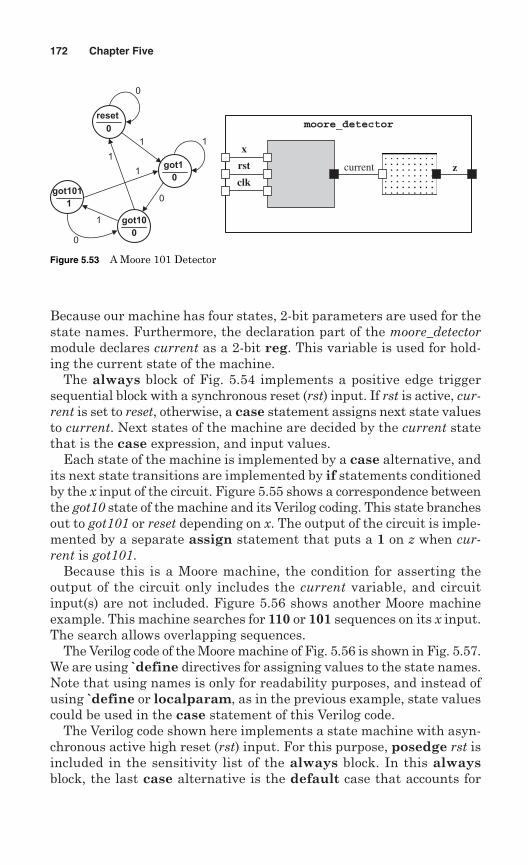
Because our machine has four states, 2-bit parameters are used for thestate names. Furthermore, the declaration part of the moore_detectormodule declares current as a 2-bit reg. This variable is used for hold-ing the current state of the machine.
The always block of Fig. 5.54 implements a positive edge triggersequential block with a synchronous reset (rst) input. If rst is active, cur-rent is set to reset, otherwise, a case statement assigns next state valuesto current. Next states of the machine are decided by the current statethat is the case expression, and input values.
Each state of the machine is implemented by a case alternative, andits next state transitions are implemented by if statements conditionedby the x input of the circuit. Figure 5.55 shows a correspondence betweenthe got10 state of the machine and its Verilog coding. This state branchesout to got101 or reset depending on x. The output of the circuit is imple-mented by a separate assign statement that puts a 1 on z when cur-rent is got101.
Because this is a Moore machine, the condition for asserting theoutput of the circuit only includes the current variable, and circuitinput(s) are not included. Figure 5.56 shows another Moore machineexample. This machine searches for 110 or 101 sequences on its x input.The search allows overlapping sequences.
The Verilog code of the Moore machine of Fig. 5.56 is shown in Fig. 5.57.We are using ̀ define directives for assigning values to the state names.Note that using names is only for readability purposes, and instead ofusing `define or localparam, as in the previous example, state valuescould be used in the case statement of this Verilog code.
The Verilog code shown here implements a state machine with asyn-chronous active high reset (rst) input. For this purpose, posedge rst isincluded in the sensitivity list of the always block. In this alwaysblock, the last case alternative is the default case that accounts for
172 Chapter Five
got1
0
got101
1
got10
0
reset
0
0
1 1
0
1
1
1
0
moore_detector
x
rst
clkcurrent z
Figure 5.53 A Moore 101 Detector
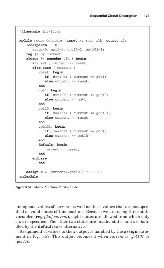
ambiguous values of current, as well as those values that are not spec-ified as valid states of this machine. Because we are using three statevariables (reg [2:0] current), eight states are allowed from which onlysix are specified. The other two states are invalid states and are han-dled by the default case alternative.
Assignment of values to the z output is handled by the assign state-ment in Fig. 5.57. This output becomes 1 when current is `got101 or`got110.
Sequential Circuit Description 173
`timescale 1ns/100ps
module moore_detector (input x, rst, clk, output z);localparam [1:0]
reset=0, got1=1, got10=2, got101=3;reg [1:0] current;always @( posedge clk ) begin
if( rst ) current <= reset;else case ( current )
reset: beginif( x==1’b1 ) current <= got1;else current <= reset;
endgot1: begin
if( x==1’b0 ) current <= got10;else current <= got1;
endgot10: begin
if( x==1’b1 ) current <= got101;else current <= reset;
endgot101: begin
if( x==1’b1 ) current <= got1;else current <= got10;
enddefault: begin
current <= reset;end
endcaseend
assign z = (current==got101) ? 1 : 0;endmodule
Figure 5.54 Moore Machine Verilog Code
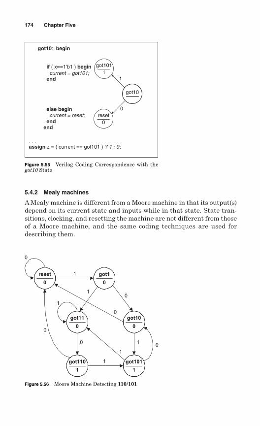
5.4.2 Mealy machines
A Mealy machine is different from a Moore machine in that its output(s)depend on its current state and inputs while in that state. State tran-sitions, clocking, and resetting the machine are not different from thoseof a Moore machine, and the same coding techniques are used fordescribing them.
174 Chapter Five
got1011
resetcurrent = reset;
current = got101;
0
got10
1
0
got10: begin
if ( x==1'b1 ) begin
end
else begin
endend
. . . assign z = ( current == got101 ) ? 1 : 0;
Figure 5.55 Verilog Coding Correspondence with thegot10 State
reset
0
0
1
got11
0
got110
1
got1
0
got10
0
got101
1
10
0
10
1
1
0
1
0
Figure 5.56 Moore Machine Detecting 110/101
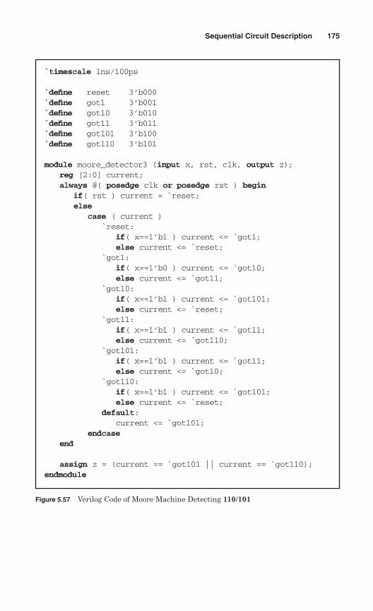
Sequential Circuit Description 175
`timescale 1ns/100ps
`define reset 3’b000`define got1 3’b001`define got10 3’b010`define got11 3’b011`define got101 3’b100`define got110 3’b101
module moore_detector3 (input x, rst, clk, output z);reg [2:0] current;always @( posedge clk or posedge rst ) begin
if( rst ) current = `reset;else
case ( current )`reset:
if( x==1’b1 ) current <= `got1;else current <= `reset;
`got1:if( x==1’b0 ) current <= `got10;else current <= `got11;
`got10:if( x==1’b1 ) current <= `got101;else current <= `reset;
`got11:if( x==1’b1 ) current <= `got11;else current <= `got110;
`got101:if( x==1’b1 ) current <= `got11;else current <= `got10;
`got110:if( x==1’b1 ) current <= `got101;else current <= `reset;
default:current <= `got101;
endcaseend
assign z = (current == `got101 || current == `got110);endmodule
Figure 5.57 Verilog Code of Moore Machine Detecting 110/101
Figure 5.58 shows a 101 Mealy sequence detector and its correspon-ding Verilog code block diagram. This circuit has a synchronous rstinput that resets the machine to its reset state.
The Verilog code of Fig. 5.59 corresponds to this Mealy machine. A2-bit localparam construct is used for defining the states of this machine.Because the machine has three states and two state variables are usedto represent them, one combination (i.e., 11) of the state variablesbecomes unused. As in the previous example, the default in the casestatement of this Verilog code handles this unspecified combination andambiguous values that may appear on current.
The coding of the states and output of this machine are illustrated inFig. 5.60. Each state is specified by a case alternative of a case state-ment for which current is its case expression. Transitions to the nextstates of the machine are handled by if-else statements. The output ofthe machine is set to 1 using an assign statement that uses a conditionalexpression on its right-hand side. This conditional expression uses thecircuit input as well as the current state of the machine.
5.4.3 Huffman coding style
The Huffman model for a digital system characterizes it as a combina-tional block with feedbacks through an array of registers. According tothe Huffman model, Verilog coding of digital systems uses an alwaysstatement for describing the register part and another concurrent state-ment for describing the combinational part. This coding style and theMoore machine example that we will use in this section are shown inFig. 5.61. As shown, the combinational block uses x and p_state as inputand generates z and n_state. The sequential block clocks n_state intop_state, and resets p_state when rst is active.
Figure 5.62 shows the Verilog code of the state diagram of Fig. 5.61 accord-ing to the partitioning shown. In this code a localparam declaration
176 Chapter Five
got1
got10
reset
0/0
1/0
0/0
0/0
1/0
1/1
mealy_detector
x
rst
clk
current z
Figure 5.58 A 101 Mealy Machine
declares the states of the machine. Following this declaration, n_stateand p_state variables are declared as 2-bit regs that hold values corre-sponding to the states of the 101 Moore detector. The combinationalalways block follows this reg declaration. Since this a purely combi-national block, it is sensitive to all its inputs, namely x and p_state.Immediately following the block heading, n_state and z are set to theirinactive or reset values. This is done so that these variables are alwaysrefreshed with new values and never retain their old values. As dis-cussed before, retaining old values implies latches, which is not whatwe want in our combinational block.
Sequential Circuit Description 177
`timescale 1ns/100ps
module mealy_detector2 (input x, rst, clk, output z);
localparam [1:0]reset = 0, // 0 = 0 0got1 = 1, // 1 = 0 1got10 = 2; // 2 = 1 0
reg [1:0] current;
always @( posedge clk ) beginif (rst) current <= reset;else case ( current )
reset:if( x==1’b1 ) current <= got1;else current <= reset;
got1:if( x==1’b0 ) current <= got10;else current <= got1;
got10:if( x==1’b1 ) current <= got1;else current <= reset;
default:current <= reset;
endcaseend
assign z = ( current==got10 && x==1’b1 ) ? 1’b1 : 1’b0;
endmodule
Figure 5.59 Verilog Code for a 101 Mealy Machine
The body of the combinational always block of Fig. 5.62 contains a casestatement that uses the p_state input of the always block for its caseexpression. This expression is checked against the states of the Mooremachine. As in the other styles discussed before, this case-statement hascase alternatives for reset, got1, got10, and got101 states.
In a block corresponding to a particular case alternative, based oninput values, values are assigned to n_state and z output. Unlike theother styles where current is used both for the present and next states,here we use two different variables, p_state and n_state.
The next procedural block shown in Fig. 5.62 handles the register(sequential) part of the Huffman model of Fig. 5.61. In this part, n_state
178 Chapter Five
got10:
if (x == 1'b1)current = got1;
else
current = reset;
...assign z = (current == got10 && x == 1) ? 1:0;
got1
got10
reset0/0
1/1
Figure 5.60 Mealy State Coding
got1
0
got101
1
got10
0
reset
0
0
1 1
0
1
1
1
0
moore_detector
x
n_state[1:0]
clk
p_state[1:0]
z
rst
combinational
sequential
Figure 5.61 Huffman Style of Coding a State Machine
Sequential Circuit Description 179
`timescale 1ns/100ps
module moore_detector4 (input x, rst, clk, output reg z);
localparam [1:0]reset=2’b00, got1=2’b01, got10=2’b10, got101=2’b11;
reg [1:0] p_state, n_state;
always @( p_state or x ) begin:combinationaln_state = reset;z = 1’b0;case ( p_state )
reset:begin
if( x==1’b1 ) n_state = got1;else n_state = reset;z = 1’b0;
endgot1:
beginif( x==1’b0 ) n_state = got10;else n_state = got1;z = 1’b0;
endgot10:
beginif( x==1’b1 ) n_state = got101;else n_state = reset;z = 1’b0;
endgot101:
beginif( x==1’b1 ) n_state = got1;else n_state = got10;z = 1’b1;
enddefault:
beginn_state = reset;z = 1’b0;
endendcase
end (Continued)
Figure 5.62 Moore Detector Verilog Code According to Huffman Model
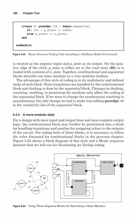
is treated as the register input and p_state as its output. On the posi-tive edge of the clock, p_state is either set to the reset state (00) or isloaded with contents of n_state. Together, combinational and sequentialblocks describe our state machine in a very modular fashion.
The advantage of this style of coding is in its modularity and definedtasks of each block. State transitions are handled by the combinationalblock and clocking is done by the sequential block. Changes in clocking,resetting, enabling, or presetting the machine only affect the coding ofthe sequential block. If we were to change the synchronous resetting toasynchronous, the only change we had to make was adding posedge rstto the sensitivity list of the sequential block.
5.4.4 A more modular style
For a design with more input and output lines and more complex outputlogic, the combinational block may further be partitioned into a blockfor handling transitions and another for assigning values to the outputsof the circuit. For coding both of these blocks, it is necessary to followthe rules discussed for combinational blocks in the previous chapter.Figure 5.63 shows a block diagram of this style and a Mealy sequencedetector that we will use for illustrating its Verilog coding.
180 Chapter Five
always @( posedge clk ) begin:sequentialif( rst ) p_state <= reset;else p_state <= n_state;
end
endmodule
Figure 5.62 Moore Detector Verilog Code According to Huffman Model (Continued)
got1
got10
reset
0/0
1/0
1/0
0/0
0/0
1/1
got11
1/0
0/1
mealy_detector
x
n_state[1:0]sequential
clk
p_state[1:0]
z
rst
combinational output_block
Figure 5.63 Using Three Separate Blocks for Describing a State Machine
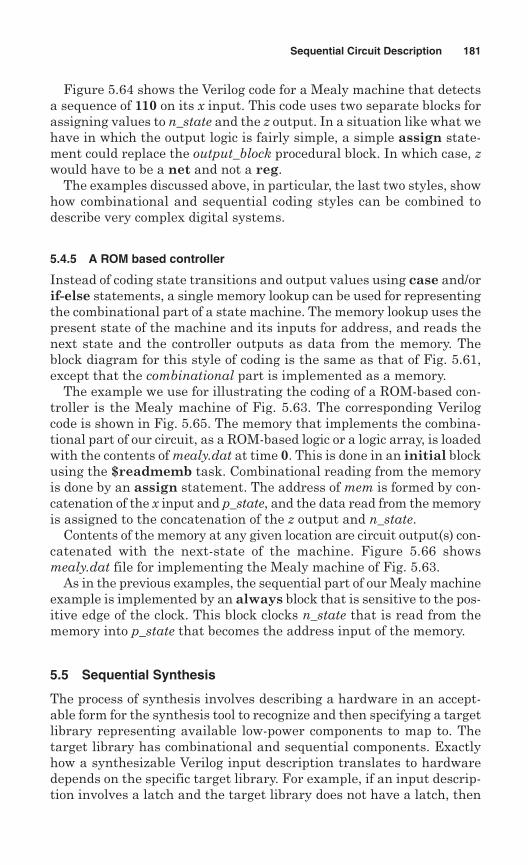
Figure 5.64 shows the Verilog code for a Mealy machine that detectsa sequence of 110 on its x input. This code uses two separate blocks forassigning values to n_state and the z output. In a situation like what wehave in which the output logic is fairly simple, a simple assign state-ment could replace the output_block procedural block. In which case, zwould have to be a net and not a reg.
The examples discussed above, in particular, the last two styles, showhow combinational and sequential coding styles can be combined todescribe very complex digital systems.
5.4.5 A ROM based controller
Instead of coding state transitions and output values using case and/orif-else statements, a single memory lookup can be used for representingthe combinational part of a state machine. The memory lookup uses thepresent state of the machine and its inputs for address, and reads thenext state and the controller outputs as data from the memory. Theblock diagram for this style of coding is the same as that of Fig. 5.61,except that the combinational part is implemented as a memory.
The example we use for illustrating the coding of a ROM-based con-troller is the Mealy machine of Fig. 5.63. The corresponding Verilogcode is shown in Fig. 5.65. The memory that implements the combina-tional part of our circuit, as a ROM-based logic or a logic array, is loadedwith the contents of mealy.dat at time 0. This is done in an initial blockusing the $readmemb task. Combinational reading from the memoryis done by an assign statement. The address of mem is formed by con-catenation of the x input and p_state, and the data read from the memoryis assigned to the concatenation of the z output and n_state.
Contents of the memory at any given location are circuit output(s) con-catenated with the next-state of the machine. Figure 5.66 showsmealy.dat file for implementing the Mealy machine of Fig. 5.63.
As in the previous examples, the sequential part of our Mealy machineexample is implemented by an always block that is sensitive to the pos-itive edge of the clock. This block clocks n_state that is read from thememory into p_state that becomes the address input of the memory.
5.5 Sequential Synthesis
The process of synthesis involves describing a hardware in an accept-able form for the synthesis tool to recognize and then specifying a targetlibrary representing available low-power components to map to. Thetarget library has combinational and sequential components. Exactlyhow a synthesizable Verilog input description translates to hardwaredepends on the specific target library. For example, if an input descrip-tion involves a latch and the target library does not have a latch, then
Sequential Circuit Description 181
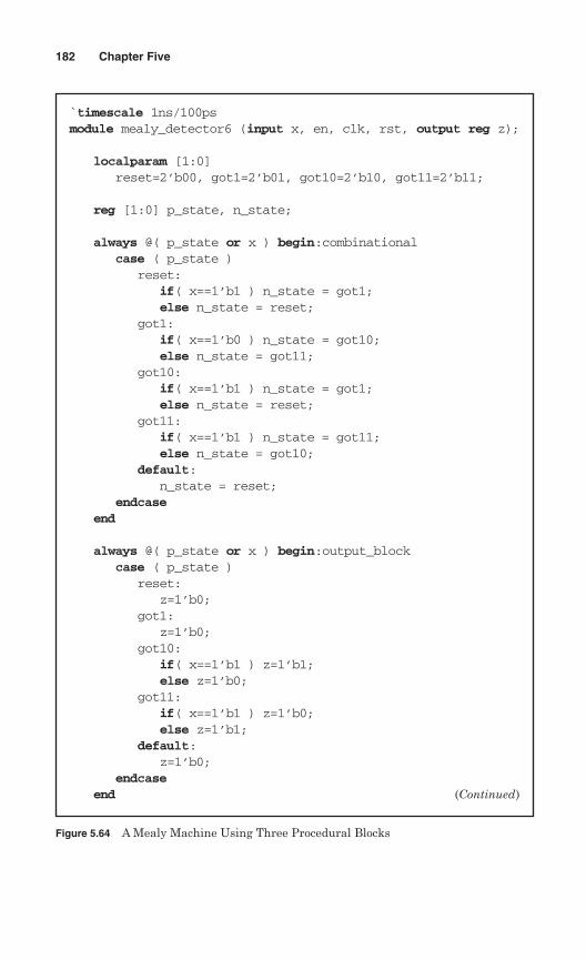
182 Chapter Five
`timescale 1ns/100psmodule mealy_detector6 (input x, en, clk, rst, output reg z);
localparam [1:0]reset=2’b00, got1=2’b01, got10=2’b10, got11=2’b11;
reg [1:0] p_state, n_state;
always @( p_state or x ) begin:combinationalcase ( p_state )
reset:if( x==1’b1 ) n_state = got1;else n_state = reset;
got1:if( x==1’b0 ) n_state = got10;else n_state = got11;
got10:if( x==1’b1 ) n_state = got1;else n_state = reset;
got11:if( x==1’b1 ) n_state = got11;else n_state = got10;
default:n_state = reset;
endcaseend
always @( p_state or x ) begin:output_blockcase ( p_state )
reset:z=1’b0;
got1:z=1’b0;
got10:if( x==1’b1 ) z=1’b1;else z=1’b0;
got11:if( x==1’b1 ) z=1’b0;else z=1’b1;
default:z=1’b0;
endcaseend (Continued)
Figure 5.64 A Mealy Machine Using Three Procedural Blocks
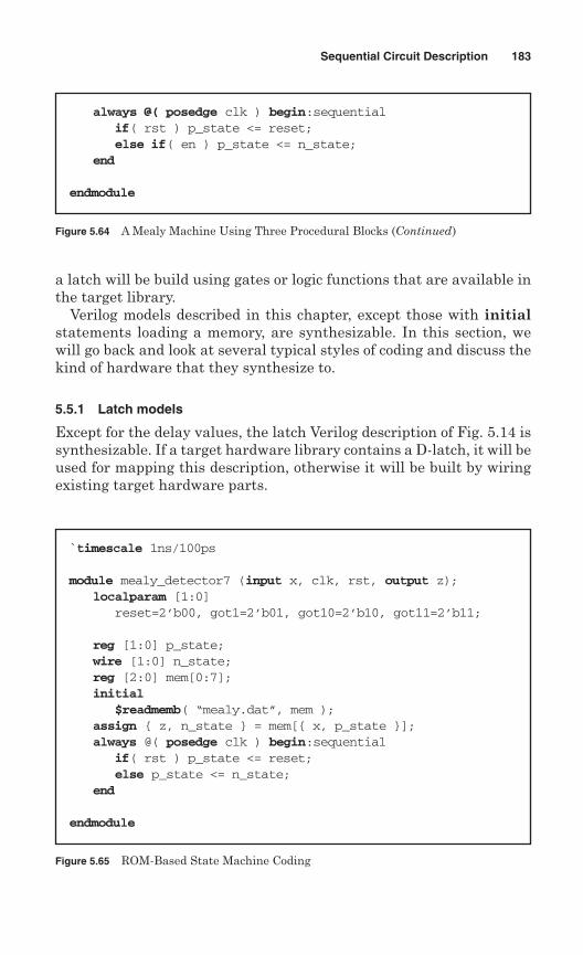
a latch will be build using gates or logic functions that are available inthe target library.
Verilog models described in this chapter, except those with initialstatements loading a memory, are synthesizable. In this section, wewill go back and look at several typical styles of coding and discuss thekind of hardware that they synthesize to.
5.5.1 Latch models
Except for the delay values, the latch Verilog description of Fig. 5.14 issynthesizable. If a target hardware library contains a D-latch, it will beused for mapping this description, otherwise it will be built by wiringexisting target hardware parts.
Sequential Circuit Description 183
always @( posedge clk ) begin:sequentialif( rst ) p_state <= reset;else if( en ) p_state <= n_state;
end
endmodule
Figure 5.64 A Mealy Machine Using Three Procedural Blocks (Continued)
`timescale 1ns/100ps
module mealy_detector7 (input x, clk, rst, output z);localparam [1:0]
reset=2’b00, got1=2’b01, got10=2’b10, got11=2’b11;
reg [1:0] p_state;wire [1:0] n_state;reg [2:0] mem[0:7];initial
$readmemb( “mealy.dat”, mem );assign { z, n_state } = mem[{ x, p_state }];always @( posedge clk ) begin:sequential
if( rst ) p_state <= reset;else p_state <= n_state;
end
endmodule
Figure 5.65 ROM-Based State Machine Coding
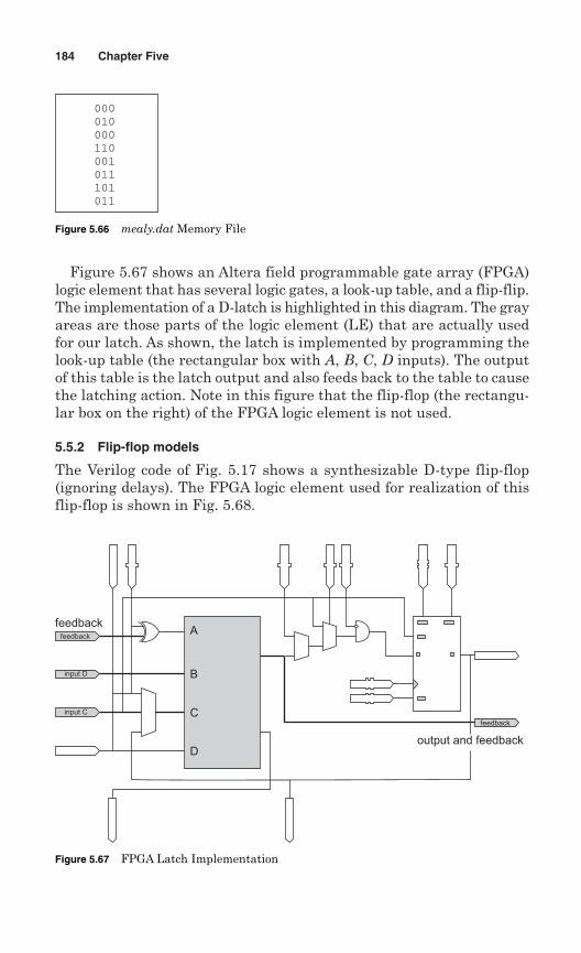
Figure 5.67 shows an Altera field programmable gate array (FPGA)logic element that has several logic gates, a look-up table, and a flip-flip.The implementation of a D-latch is highlighted in this diagram. The grayareas are those parts of the logic element (LE) that are actually usedfor our latch. As shown, the latch is implemented by programming thelook-up table (the rectangular box with A, B, C, D inputs). The outputof this table is the latch output and also feeds back to the table to causethe latching action. Note in this figure that the flip-flop (the rectangu-lar box on the right) of the FPGA logic element is not used.
5.5.2 Flip-flop models
The Verilog code of Fig. 5.17 shows a synthesizable D-type flip-flop(ignoring delays). The FPGA logic element used for realization of thisflip-flop is shown in Fig. 5.68.
184 Chapter Five
000010000110001011101011
Figure 5.66 mealy.dat Memory File
feedback
output and feedback
A
B
C
D
feedback
feedback
input D
input C
Figure 5.67 FPGA Latch Implementation
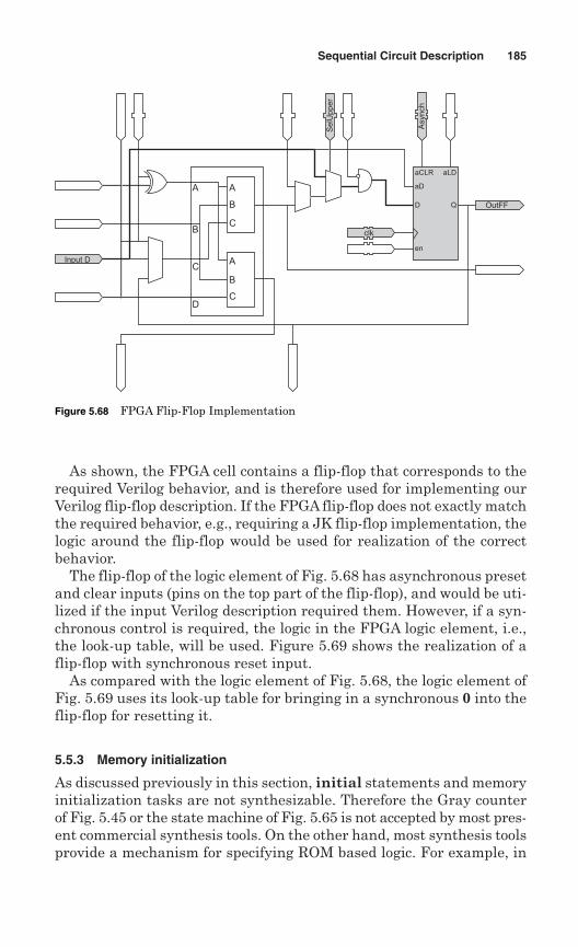
As shown, the FPGA cell contains a flip-flop that corresponds to therequired Verilog behavior, and is therefore used for implementing ourVerilog flip-flop description. If the FPGA flip-flop does not exactly matchthe required behavior, e.g., requiring a JK flip-flop implementation, thelogic around the flip-flop would be used for realization of the correctbehavior.
The flip-flop of the logic element of Fig. 5.68 has asynchronous presetand clear inputs (pins on the top part of the flip-flop), and would be uti-lized if the input Verilog description required them. However, if a syn-chronous control is required, the logic in the FPGA logic element, i.e.,the look-up table, will be used. Figure 5.69 shows the realization of aflip-flop with synchronous reset input.
As compared with the logic element of Fig. 5.68, the logic element ofFig. 5.69 uses its look-up table for bringing in a synchronous 0 into theflip-flop for resetting it.
5.5.3 Memory initialization
As discussed previously in this section, initial statements and memoryinitialization tasks are not synthesizable. Therefore the Gray counterof Fig. 5.45 or the state machine of Fig. 5.65 is not accepted by most pres-ent commercial synthesis tools. On the other hand, most synthesis toolsprovide a mechanism for specifying ROM based logic. For example, in
Sequential Circuit Description 185
Asynch
SelU
pper
aCLR aLD
aD
D Q
en
A A
B
C
A
B
C
B
C
D
Input D
clk
OutFF
Figure 5.68 FPGA Flip-Flop Implementation
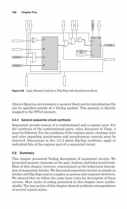
Altera’s Quartus environment a memory block and its initialization filecan be specified outside of a Verilog module. This memory is directlymapped to the FPGA memory.
5.5.4 General sequential circuit synthesis
Sequential circuits consist of a combinational and a register part. Forthe synthesis of the combinational parts, rules discussed in Chap. 4must be followed. For the synthesis of the register parts, clocking rulesand rules regarding synchronous and asynchronous controls must beobserved. Discussions in Sec. 5.5.2 about flip-flop synthesis, apply toindividual bits of the register part of a sequential circuit.
5.6 Summary
This chapter presented Verilog description of sequential circuits. Wepresented memory elements at the gate, boolean and behavioral levels.Most of this chapter, however, concentrated on the behavioral descrip-tion of sequential circuits. We discussed sequential circuits as simple aslatches and flip-flops and as complex as queues and sequence detectors.We showed that we follow the same basic rules for description of thesecircuits. Most styles of coding presented in this chapter were synthe-sizable. The last section of this chapter showed synthesis correspondenceof several typical styles.
186 Chapter Five
Asyn
ch
Input C
clk
OutFF
Input D
A
B
C
D
aCLR aLD
aD
D Q
en
Figure 5.69 Logic Element Used for a Flip-Flop with Synchronous Reset
Problems
5.1 Show Verilog code of an SR-latch with active low set and reset inputs.
5.2 Write a negative edge trigger D-type flip-flop with an asynchronous active-low reset, a synchronous active-high set, and an active-high clock enable input.
5.3 Write a 32 word register file in Verilog which reads its data from a file nameddata.mem. It has a 5-bit address input named index and a read input signal. Whenthe read input is 1, the output of the memory is equal to the data written in theindex address of the register file, otherwise the output equals 8’bZZ.
5.4 Show synthesizable Verilog code for a register unit that performsoperations shown below. The unit has a 3-bit mode (md) input, an asynchronousreset (rs) input, a 1-bit output control (oc) input, and an 8-bit bidirectional iobus. The internal register drives the io bus when oc is 1 and md is not 111.
md=000: does nothing
md=001: right shift the register
md=010: left shift the register
md=011: up count, Gray (000, 001, 011, 010, 110, 111, 101, 100)
md=100: down count, Gray (opposite of the above)
md=101: complement register contents
md=110: swap right and left 4 bits
md=111: parallel load
5.5 Design an 8-bit shifter with parallel input and output, sin_l, sin_r input lines,and shift and parallel control signals. When the shift signal is issued, data on sin_land sin_r lines will be entered to the most and least significant bits of the registerrespectively, and third and fourth bits of the register will be put on a 2-bit outputline named out. No shifting will be done if the unit is in parallel mode.
5.6 Show the Verilog code of the following up-down counter. The counter hasa u input that controls its count direction. If u is 1, it counts 010, 011, 101, 011,111, 001 ... . If u is 0, it counts this same sequence in the opposite direction.
5.7 Show Verilog code for a 4-bit counter that counts the following sequence:0100, 0001, 1011, 1010, 0111, 1111, 0111, 0000, 1000. Write this according tothe Huffman model in which the logic part is separate from the register part.Code the logic part by a memory, mem, that is initialized in a procedural blockusing the $readmemh system task. This task should read the contents ofmem.dat file and load it into mem. Show the complete Verilog code and contentsof the memory file.
5.8 Write Verilog description for an 8-word FILO stack with 8-bit input andoutput data lines and rd and wr input signals. The stack has a full output flag,that when it becomes 1, the stack cannot accept any more data.
Sequential Circuit Description 187
5.9 Show the Verilog code for a Moore 100110 detector using the Huffman styleof coding.
5.10 Show the design of a Mealy machine sequence detector that detects the100 and 001 sequences on its serial input. Provide an asynchronous reset inputthat starts the detector in its first state.
5.11 A sequential circuit has a synchronizing input, s, and two data inputs aand b that are treated as a 2-bit binary number ({a,b}). After a start sequenceof 110 on s, the machine starts adding data on the data inputs and produces themodulo-4 add result of all the data received on the data inputs. This continuesuntil an end sequence, 011, is received on s. At this time the machine goes intothe halt state and ignores all the data on its a and b inputs. While in this state,the machine searches for the start sequence on s. The start and end sequencesdo not overlap. Write a Verilog description for this circuit.
5.12 A simple sequential multiplier is developed by adding A to itself B numberof times. Both A and B inputs are 8-bit unsigned numbers. The circuit has a startinput that becomes 1 for one clock when the inputs are valid. The inputs willnot be valid when this signal is 0. After the start, the circuit sets its done outputto 0 and starts the multiplication process. When done, it puts the result on Rand sets done to 1. Given the following interface, write the complete code of thismultiplier.
5.13 A data collector module has seven data registers of length 15 driving itsseven 15-bit outputs. This module has ser_data serial input, data_ready inputindicating when the stream of data is available on ser_data, and the busyoutput. A 112 (112 = 7*15 + 4 + 3) bit packet starts on ser_data when data_readybecomes 1. A packet starts with its header that includes 4 bits for m, followedby 3 bits for n, and it is then followed by n*m data bits. The data bits of a packetconstitute n m-bit data words. Bits of data words are arranged from least to most.There are always fewer than 8 data words (n <= 7) and each data-word has lessthan 16 bits (m <= 15). After the header, the first m bits are those of data-word 1,immediately followed by m bits of data-word 2, and at the end, m bits of data-word n. Your module should separate the data words and put them in its 15registers. The registers should be left-filled with 0s for m<15. For n of less than 7,
188 Chapter Five
module mult (a, b, start, clk, r, done);input [7:0] a, b;input start, clk;output [15:0] r;output done;reg [7:0] abuf, bbuf; // use these if you likereg [15:0] r;. . .endmodule
only the first n registers will be filled and the rest will be filled with zeros.Write a synthesizable DataCollector module.
5.14 Write an always statement to count the number of 1s in a given reg[255:0] InVec. Declare all necessary registers and wires. The system clock (clk)is available for you to use.
5.15 An important issue in CPU modeling and testing is modeling of itsmemory. Because of machine memory limitations, a CPU memory must bemodeled to use external files. In this problem you are to write a memory modelthat initially reads hexadecimal data from an external file, mem_file.dat, andholds it in its internal buffer. Data being read from the memory will be read fromthe buffer and data being written into the memory will be written into thebuffer and into the external memory file, mem_file.dat, at the same time. Assumethe data in mem_file.dat is for the first 256 words of the memory. You are toimplement this memory for addresses 0 to 255 only, and reading from addressesoutside of this range will return Xs. The memory model will ignore writingoutside of this range. Use the module declaration shown below.
Suggested Reading
Brown, S., and Z. Vranesic, Fundamentals of Digital Logic with Verilog Design, McGraw-Hill, New York, 2002, ISBN: 0-07-283878-7.
IEEE Std 1364-2001, IEEE Standard Verilog Language Reference Manual, SH94921-TBR (print) SS94921-TBR (electronic), ISBN 0-7381-2827-9 (print and electronic),2001.
Navabi, Z., Verilog Computer-Based Training Course, CBT CD with hardcopy User’smanual, McGraw-Hill, 2002, ISBN 0-07-137473-6.
Nelson, V. P., H. T. Nagle, B. D. Carroll, and et al., Digital Logic Circuit Analysis &Design, Prentice-Hall, Inc., New Jersey, 1996.
Sequential Circuit Description 189
module memory (mem_wr, mem_rd, databus, adbus);input mem_wr, mem_rd;inout [7:0] databus ;input [15:0] adbus;. . .endmodule

This page intentionally left blank
Chapter
6Component Test and Verification
The previous chapters discussed Verilog for describing combinationaland sequential circuits. Except in a few cases, where we dealt withtiming of modules, language constructs we discussed were synthesiz-able. This chapter discusses the use of the Verilog language for testingdesign modules. We will see that timing and display procedures becomemore important when dealing with testbench modules.
This chapter shows how Verilog language constructs can be used forapplication of data to a module under test (MUT), and how moduleresponses can be displayed and checked. In the first part of this chapterdata application and response monitoring are discussed. In the second part,we discuss the use of assertion verification for giving a better observabil-ity to our design modules. Advanced utilization of external files for test-ing will be put off until Chap. 8, where system design and test is described.
6.1 Testbench
Verilog simulation environments provide tools for graphical or textualdisplay of simulation results. Some simulation environments go fur-ther, and provide graphical tools for editing input test data to a designmodule that is being tested. Such tools are referred to as waveform edi-tors, and are usually good for small designs. They become too complexto use for a design with many busses and control signals. Another prob-lem with waveform editors is that each simulation environment uses adifferent procedure for waveform editing, and moving from one simu-lator to another requires relearning a whole new set of procedures.
This problem can be alleviated by use of Verilog testbenches. A Verilogtestbench is a Verilog module that instantiates an MUT, applies data toit, and monitors its output. Because a testbench is in Verilog, it can go from
191
Copyright © 2006 by The McGraw-Hill Publishing Companies, Inc. Click here for terms of use.
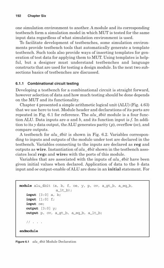
one simulation environment to another. A module and its correspondingtestbench form a simulation model in which MUT is tested for the sameinput data regardless of what simulation environment is used.
To facilitate development of testbenches, some simulation environ-ments provide testbench tools that automatically generate a templatetestbench. Such tools also provide ways of inserting templates for gen-eration of test data for applying them to MUT. Using templates is help-ful, but a designer must understand testbenches and languageconstructs that are used for testing a design module. In the next two sub-sections basics of testbenches are discussed.
6.1.1 Combinational circuit testing
Developing a testbench for a combinational circuit is straight forward,however selection of data and how much testing should be done dependson the MUT and its functionality.
Chapter 4 presented a simple arithmetic logical unit (ALU) (Fig. 4.63)that we use here to test. Module header and declarations of its ports arerepeated in Fig. 6.1 for reference. The alu_4bit module is a four func-tion ALU. Data inputs are a and b, and its function input is f. In addi-tion to its y data output, the ALU generates parity (p), overflow (ov), andcompare outputs.
A testbench for alu_4bit is shown in Fig. 6.2. Variables correspon-ding to inputs and outputs of the module under test are declared in thetestbench. Variables connecting to the inputs are declared as reg andoutputs as wire. Instantiation of alu_4bit shown in the testbench asso-ciates local regs and wires with the ports of this module.
Variables that are associated with the inputs of alu_4bit have beengiven initial values when declared. Application of data to the b datainput and oe output-enable of ALU are done in an initial statement. For
192 Chapter Six
Figure 6.1 alu_4bit Module Declaration
module alu_4bit (a, b, f, oe, y, p, ov, a_gt_b, a_eq_b,a_lt_b);
input [3:0] a, b;input [1:0] f;input oe;output [3:0] y;output p, ov, a_gt_b, a_eq_b, a_lt_b;
// . . .
endmodule
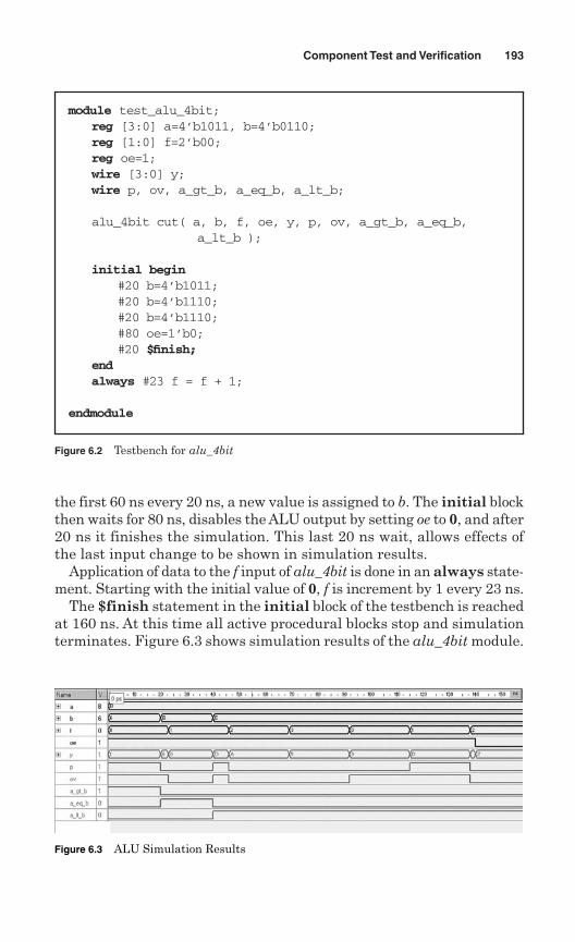
the first 60 ns every 20 ns, a new value is assigned to b. The initial blockthen waits for 80 ns, disables the ALU output by setting oe to 0, and after20 ns it finishes the simulation. This last 20 ns wait, allows effects ofthe last input change to be shown in simulation results.
Application of data to the f input of alu_4bit is done in an always state-ment. Starting with the initial value of 0, f is increment by 1 every 23 ns.
The $finish statement in the initial block of the testbench is reachedat 160 ns. At this time all active procedural blocks stop and simulationterminates. Figure 6.3 shows simulation results of the alu_4bit module.
Component Test and Verification 193
Figure 6.2 Testbench for alu_4bit
module test_alu_4bit;reg [3:0] a=4’b1011, b=4’b0110;reg [1:0] f=2’b00;reg oe=1;wire [3:0] y;wire p, ov, a_gt_b, a_eq_b, a_lt_b;
alu_4bit cut( a, b, f, oe, y, p, ov, a_gt_b, a_eq_b,a_lt_b );
initial begin#20 b=4’b1011;#20 b=4’b1110;#20 b=4’b1110;#80 oe=1’b0;#20 $finish;
endalways #23 f = f + 1;
endmodule
Figure 6.3 ALU Simulation Results
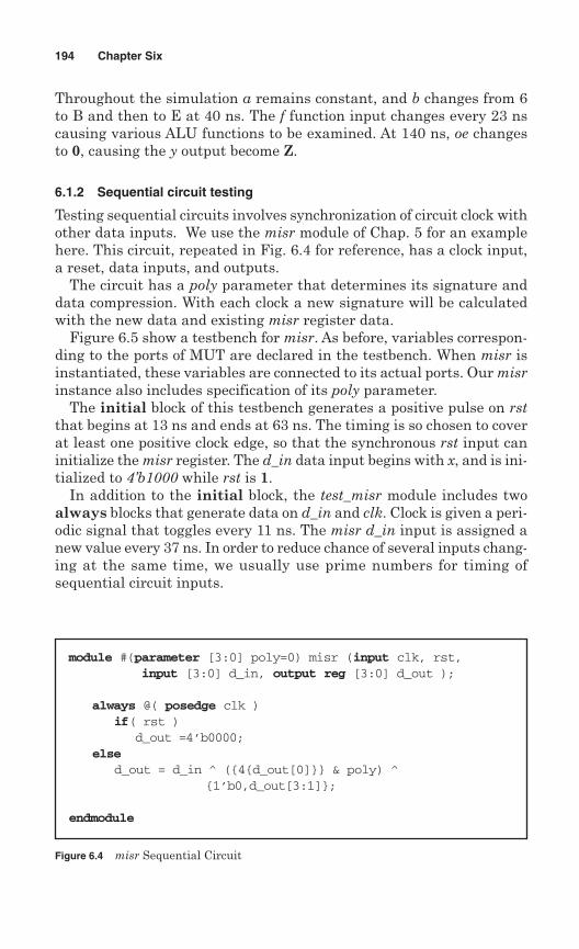
Throughout the simulation a remains constant, and b changes from 6to B and then to E at 40 ns. The f function input changes every 23 nscausing various ALU functions to be examined. At 140 ns, oe changesto 0, causing the y output become Z.
6.1.2 Sequential circuit testing
Testing sequential circuits involves synchronization of circuit clock withother data inputs. We use the misr module of Chap. 5 for an examplehere. This circuit, repeated in Fig. 6.4 for reference, has a clock input,a reset, data inputs, and outputs.
The circuit has a poly parameter that determines its signature anddata compression. With each clock a new signature will be calculatedwith the new data and existing misr register data.
Figure 6.5 show a testbench for misr. As before, variables correspon-ding to the ports of MUT are declared in the testbench. When misr isinstantiated, these variables are connected to its actual ports. Our misrinstance also includes specification of its poly parameter.
The initial block of this testbench generates a positive pulse on rstthat begins at 13 ns and ends at 63 ns. The timing is so chosen to coverat least one positive clock edge, so that the synchronous rst input caninitialize the misr register. The d_in data input begins with x, and is ini-tialized to 4’b1000 while rst is 1.
In addition to the initial block, the test_misr module includes twoalways blocks that generate data on d_in and clk. Clock is given a peri-odic signal that toggles every 11 ns. The misr d_in input is assigned anew value every 37 ns. In order to reduce chance of several inputs chang-ing at the same time, we usually use prime numbers for timing ofsequential circuit inputs.
194 Chapter Six
Figure 6.4 misr Sequential Circuit
module #(parameter [3:0] poly=0) misr (input clk, rst,input [3:0] d_in, output reg [3:0] d_out );
always @( posedge clk )if( rst )
d_out =4’b0000;else
d_out = d_in ^ ({4{d_out[0]}} & poly) ^{1’b0,d_out[3:1]};
endmodule
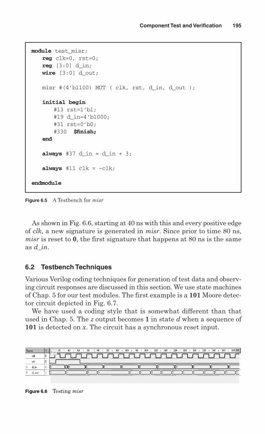
As shown in Fig. 6.6, starting at 40 ns with this and every positive edgeof clk, a new signature is generated in misr. Since prior to time 80 ns,misr is reset to 0, the first signature that happens at 80 ns is the sameas d_in.
6.2 Testbench Techniques
Various Verilog coding techniques for generation of test data and observ-ing circuit responses are discussed in this section. We use state machinesof Chap. 5 for our test modules. The first example is a 101 Moore detec-tor circuit depicted in Fig. 6.7.
We have used a coding style that is somewhat different than thatused in Chap. 5. The z output becomes 1 in state d when a sequence of101 is detected on x. The circuit has a synchronous reset input.
Component Test and Verification 195
Figure 6.5 A Testbench for misr
module test_misr;reg clk=0, rst=0;reg [3:0] d_in;wire [3:0] d_out;
misr #(4’b1100) MUT ( clk, rst, d_in, d_out );
initial begin#13 rst=1’b1;#19 d_in=4’b1000;#31 rst=0’b0; #330 $finish;
end
always #37 d_in = d_in + 3;
always #11 clk = ~clk;
endmodule
Figure 6.6 Testing misr
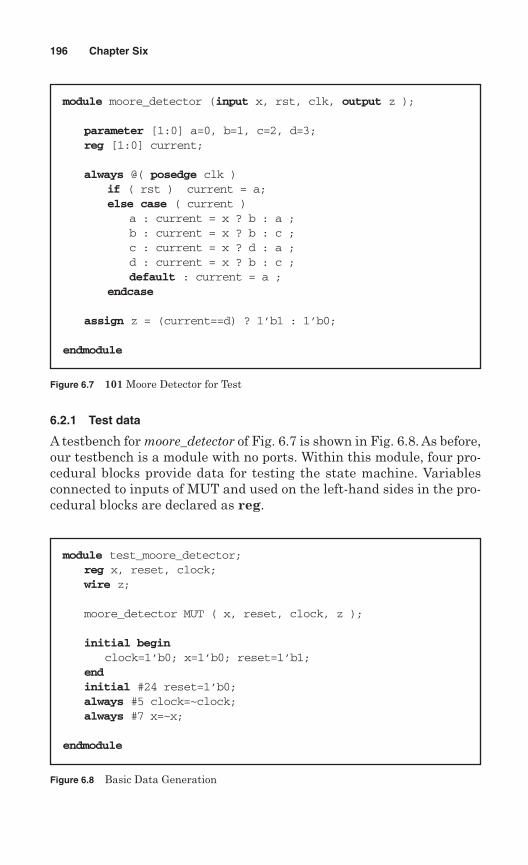
6.2.1 Test data
A testbench for moore_detector of Fig. 6.7 is shown in Fig. 6.8. As before,our testbench is a module with no ports. Within this module, four pro-cedural blocks provide data for testing the state machine. Variablesconnected to inputs of MUT and used on the left-hand sides in the pro-cedural blocks are declared as reg.
196 Chapter Six
Figure 6.7 101 Moore Detector for Test
module moore_detector (input x, rst, clk, output z );
parameter [1:0] a=0, b=1, c=2, d=3;reg [1:0] current;
always @( posedge clk )if ( rst ) current = a;else case ( current )
a : current = x ? b : a ;b : current = x ? b : c ;c : current = x ? d : a ;d : current = x ? b : c ;default : current = a ;
endcase
assign z = (current==d) ? 1’b1 : 1’b0;
endmodule
Figure 6.8 Basic Data Generation
module test_moore_detector;reg x, reset, clock;wire z;
moore_detector MUT ( x, reset, clock, z );
initial beginclock=1’b0; x=1’b0; reset=1’b1;
endinitial #24 reset=1’b0;always #5 clock=~clock;always #7 x=~x;
endmodule
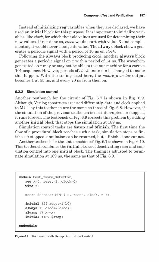
Instead of initializing reg variables when they are declared, we haveused an initial block for this purpose. It is important to initialize vari-ables, like clock, for which their old values are used for determining theirnew values. If not done so, clock would start with value X and comple-menting it would never change its value. The always block shown gen-erates a periodic signal with a period of 10 ns on clock.
Following the always block producing clock, another always blockgenerates a periodic signal on x with a period of 14 ns. The waveformgenerated on x may or may not be able to test our machine for a correct101 sequence. However, periods of clock and x can be changed to makethis happen. With the timing used here, the moore_detector outputbecomes 1 at 55 ns, and every 70 ns from then on.
6.2.2 Simulation control
Another testbench for the circuit of Fig. 6.7 is shown in Fig. 6.9.Although, Verilog constructs are used differently, data and clock appliedto MUT by this testbench are the same as those of Fig. 6.8. However, ifthe simulation of the previous testbench is not interrupted, or stopped,it runs forever. The testbench of Fig. 6.9 corrects this problem by addinganother initial block that stops the simulation at 189 ns.
Simulation control tasks are $stop and $finish. The first time theflow of a procedural block reaches such a task, simulation stops or fin-ishes. A stopped simulation can be resumed, but a finished one cannot.
Another testbench for the state machine of Fig. 6.7 is shown in Fig. 6.10.This testbench combines the initial blocks of deactivating reset and sim-ulation control into one initial block. The timing is adjusted to termi-nate simulation at 189 ns, the same as that of Fig. 6.9.
Component Test and Verification 197
Figure 6.9 Testbench with $stop Simulation Control
module test_moore_detector;reg x=0, reset=1, clock=0;wire z;
moore_detector MUT ( x, reset, clock, z );
initial #24 reset=1’b0;always #5 clock=~clock;always #7 x=~x;initial #189 $stop;
endmodule
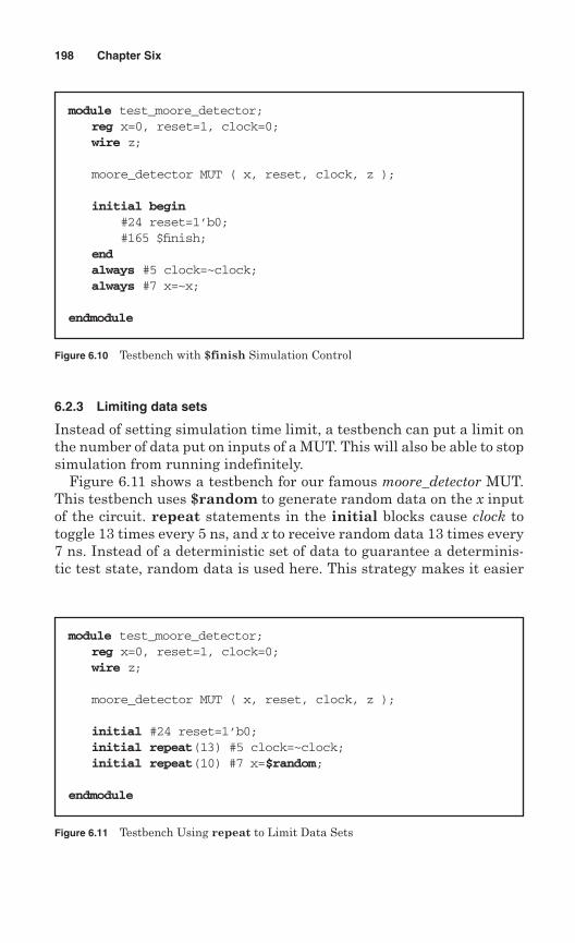
6.2.3 Limiting data sets
Instead of setting simulation time limit, a testbench can put a limit onthe number of data put on inputs of a MUT. This will also be able to stopsimulation from running indefinitely.
Figure 6.11 shows a testbench for our famous moore_detector MUT.This testbench uses $random to generate random data on the x inputof the circuit. repeat statements in the initial blocks cause clock totoggle 13 times every 5 ns, and x to receive random data 13 times every7 ns. Instead of a deterministic set of data to guarantee a determinis-tic test state, random data is used here. This strategy makes it easier
198 Chapter Six
Figure 6.10 Testbench with $finish Simulation Control
module test_moore_detector;reg x=0, reset=1, clock=0;wire z;
moore_detector MUT ( x, reset, clock, z );
initial begin#24 reset=1’b0;#165 $finish;
endalways #5 clock=~clock;always #7 x=~x;
endmodule
Figure 6.11 Testbench Using repeat to Limit Data Sets
module test_moore_detector;reg x=0, reset=1, clock=0;wire z;
moore_detector MUT ( x, reset, clock, z );
initial #24 reset=1’b0;initial repeat(13) #5 clock=~clock;initial repeat(10) #7 x=$random;
endmodule
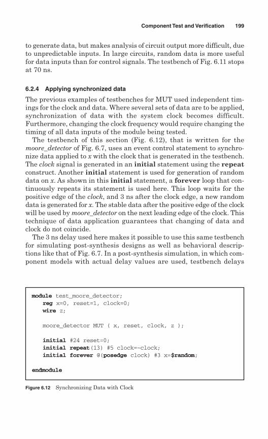
to generate data, but makes analysis of circuit output more difficult, dueto unpredictable inputs. In large circuits, random data is more usefulfor data inputs than for control signals. The testbench of Fig. 6.11 stopsat 70 ns.
6.2.4 Applying synchronized data
The previous examples of testbenches for MUT used independent tim-ings for the clock and data. Where several sets of data are to be applied,synchronization of data with the system clock becomes difficult.Furthermore, changing the clock frequency would require changing thetiming of all data inputs of the module being tested.
The testbench of this section (Fig. 6.12), that is written for themoore_detector of Fig. 6.7, uses an event control statement to synchro-nize data applied to x with the clock that is generated in the testbench.The clock signal is generated in an initial statement using the repeatconstruct. Another initial statement is used for generation of randomdata on x. As shown in this initial statement, a forever loop that con-tinuously repeats its statement is used here. This loop waits for thepositive edge of the clock, and 3 ns after the clock edge, a new randomdata is generated for x. The stable data after the positive edge of the clockwill be used by moore_detector on the next leading edge of the clock. Thistechnique of data application guarantees that changing of data andclock do not coincide.
The 3 ns delay used here makes it possible to use this same testbenchfor simulating post-synthesis designs as well as behavioral descrip-tions like that of Fig. 6.7. In a post-synthesis simulation, in which com-ponent models with actual delay values are used, testbench delays
Component Test and Verification 199
Figure 6.12 Synchronizing Data with Clock
module test_moore_detector;reg x=0, reset=1, clock=0;wire z;
moore_detector MUT ( x, reset, clock, z );
initial #24 reset=0;initial repeat(13) #5 clock=~clock;initial forever @(posedge clock) #3 x=$random;
endmodule
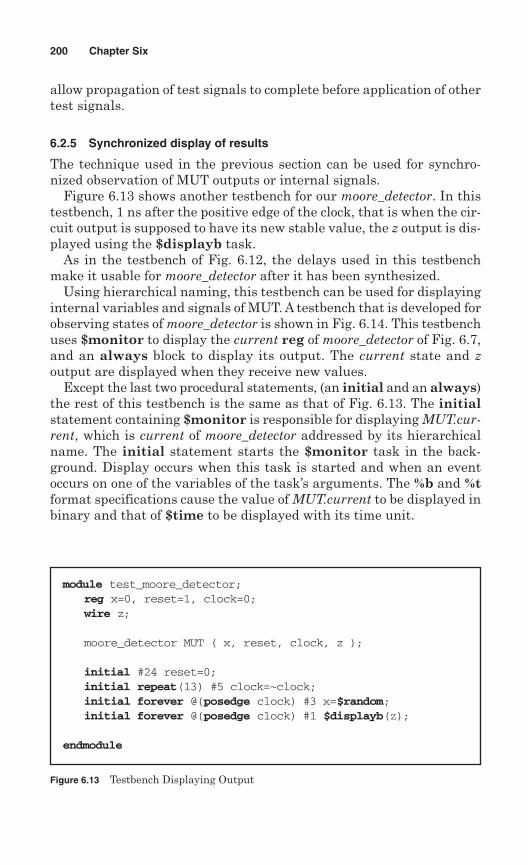
allow propagation of test signals to complete before application of othertest signals.
6.2.5 Synchronized display of results
The technique used in the previous section can be used for synchro-nized observation of MUT outputs or internal signals.
Figure 6.13 shows another testbench for our moore_detector. In thistestbench, 1 ns after the positive edge of the clock, that is when the cir-cuit output is supposed to have its new stable value, the z output is dis-played using the $displayb task.
As in the testbench of Fig. 6.12, the delays used in this testbenchmake it usable for moore_detector after it has been synthesized.
Using hierarchical naming, this testbench can be used for displayinginternal variables and signals of MUT. A testbench that is developed forobserving states of moore_detector is shown in Fig. 6.14. This testbenchuses $monitor to display the current reg of moore_detector of Fig. 6.7,and an always block to display its output. The current state and zoutput are displayed when they receive new values.
Except the last two procedural statements, (an initial and an always)the rest of this testbench is the same as that of Fig. 6.13. The initialstatement containing $monitor is responsible for displaying MUT.cur-rent, which is current of moore_detector addressed by its hierarchicalname. The initial statement starts the $monitor task in the back-ground. Display occurs when this task is started and when an eventoccurs on one of the variables of the task’s arguments. The %b and %tformat specifications cause the value of MUT.current to be displayed inbinary and that of $time to be displayed with its time unit.
200 Chapter Six
Figure 6.13 Testbench Displaying Output
module test_moore_detector;reg x=0, reset=1, clock=0;wire z;
moore_detector MUT ( x, reset, clock, z );
initial #24 reset=0;initial repeat(13) #5 clock=~clock;initial forever @(posedge clock) #3 x=$random;initial forever @(posedge clock) #1 $displayb(z);
endmodule
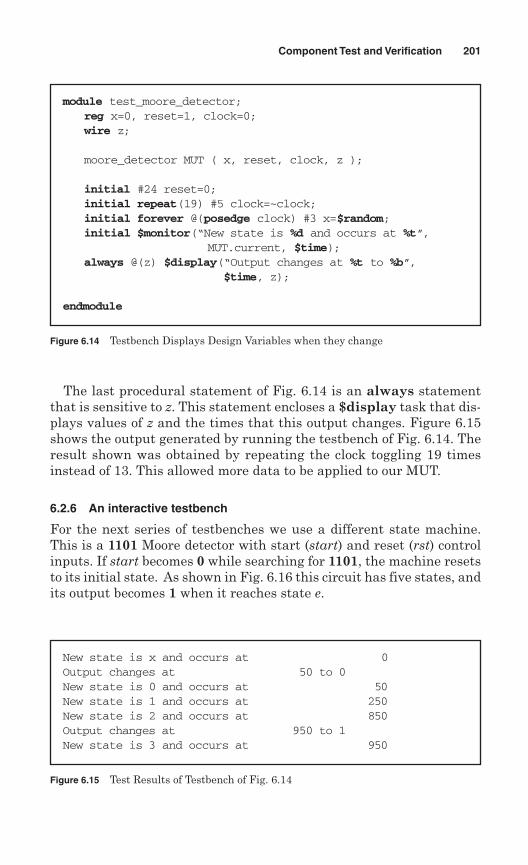
The last procedural statement of Fig. 6.14 is an always statementthat is sensitive to z. This statement encloses a $display task that dis-plays values of z and the times that this output changes. Figure 6.15shows the output generated by running the testbench of Fig. 6.14. Theresult shown was obtained by repeating the clock toggling 19 timesinstead of 13. This allowed more data to be applied to our MUT.
6.2.6 An interactive testbench
For the next series of testbenches we use a different state machine.This is a 1101 Moore detector with start (start) and reset (rst) controlinputs. If start becomes 0 while searching for 1101, the machine resetsto its initial state. As shown in Fig. 6.16 this circuit has five states, andits output becomes 1 when it reaches state e.
Component Test and Verification 201
Figure 6.14 Testbench Displays Design Variables when they change
module test_moore_detector;reg x=0, reset=1, clock=0;wire z;
moore_detector MUT ( x, reset, clock, z );
initial #24 reset=0;initial repeat(19) #5 clock=~clock;initial forever @(posedge clock) #3 x=$random;initial $monitor(“New state is %d and occurs at %t”,
MUT.current, $time);always @(z) $display(“Output changes at %t to %b”,
$time, z);
endmodule
Figure 6.15 Test Results of Testbench of Fig. 6.14
New state is x and occurs at 0Output changes at 50 to 0New state is 0 and occurs at 50New state is 1 and occurs at 250New state is 2 and occurs at 850Output changes at 950 to 1New state is 3 and occurs at 950
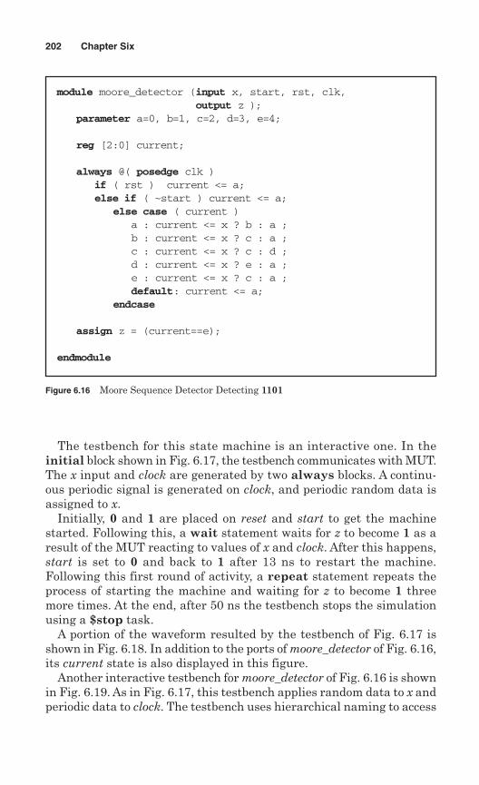
The testbench for this state machine is an interactive one. In theinitial block shown in Fig. 6.17, the testbench communicates with MUT.The x input and clock are generated by two always blocks. A continu-ous periodic signal is generated on clock, and periodic random data isassigned to x.
Initially, 0 and 1 are placed on reset and start to get the machinestarted. Following this, a wait statement waits for z to become 1 as aresult of the MUT reacting to values of x and clock. After this happens,start is set to 0 and back to 1 after 13 ns to restart the machine.Following this first round of activity, a repeat statement repeats theprocess of starting the machine and waiting for z to become 1 threemore times. At the end, after 50 ns the testbench stops the simulationusing a $stop task.
A portion of the waveform resulted by the testbench of Fig. 6.17 isshown in Fig. 6.18. In addition to the ports of moore_detector of Fig. 6.16,its current state is also displayed in this figure.
Another interactive testbench for moore_detector of Fig. 6.16 is shownin Fig. 6.19. As in Fig. 6.17, this testbench applies random data to x andperiodic data to clock. The testbench uses hierarchical naming to access
202 Chapter Six
Figure 6.16 Moore Sequence Detector Detecting 1101
module moore_detector (input x, start, rst, clk,output z );
parameter a=0, b=1, c=2, d=3, e=4;
reg [2:0] current;
always @( posedge clk )if ( rst ) current <= a;else if ( ~start ) current <= a;
else case ( current )a : current <= x ? b : a ;b : current <= x ? c : a ;c : current <= x ? c : d ;d : current <= x ? e : a ;e : current <= x ? c : a ;default: current <= a;
endcase
assign z = (current==e);
endmodule
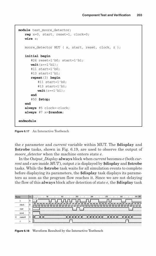
the e parameter and current variable within MUT. The $display and$strobe tasks, shown in Fig. 6.19, are used to observe the output ofmoore_detector when the machine enters state e.
In the Output_Display always block when current becomes e (both cur-rent and e are inside MUT ), output z is displayed by $display and $strobetasks. While the $strobe task waits for all simulation events to completebefore displaying its parameters, the $display task displays its parame-ters as soon as the program flow reaches it. Since we are not delayingthe flow of this always block after detection of state e, the $display task
Component Test and Verification 203
Figure 6.17 An Interactive Testbench
module test_moore_detector;reg x=0, start, reset=1, clock=0;wire z;
moore_detector MUT ( x, start, reset, clock, z );
initial begin#24 reset=1’b0; start=1’b1;wait(z==1’b1);#11 start=1’b0;#13 start=1’b1;repeat(3) begin
#11 start=1’b0;#13 start=1’b1;wait(z==1’b1);
end#50 $stop;
endalways #5 clock=~clock;always #7 x=$random;
endmodule
Figure 6.18 Waveform Resulted by the Interactive Testbench
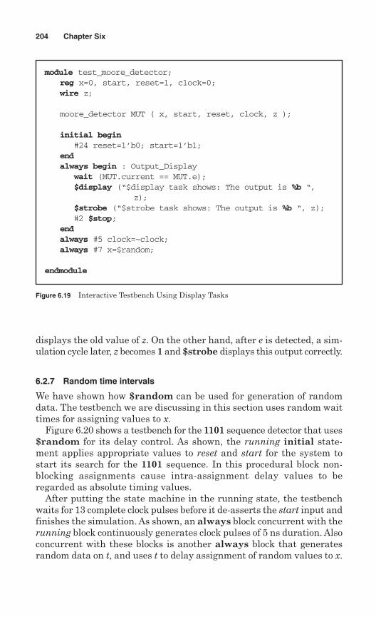
displays the old value of z. On the other hand, after e is detected, a sim-ulation cycle later, z becomes 1 and $strobe displays this output correctly.
6.2.7 Random time intervals
We have shown how $random can be used for generation of randomdata. The testbench we are discussing in this section uses random waittimes for assigning values to x.
Figure 6.20 shows a testbench for the 1101 sequence detector that uses$random for its delay control. As shown, the running initial state-ment applies appropriate values to reset and start for the system tostart its search for the 1101 sequence. In this procedural block non-blocking assignments cause intra-assignment delay values to beregarded as absolute timing values.
After putting the state machine in the running state, the testbenchwaits for 13 complete clock pulses before it de-asserts the start input andfinishes the simulation. As shown, an always block concurrent with therunning block continuously generates clock pulses of 5 ns duration. Alsoconcurrent with these blocks is another always block that generatesrandom data on t, and uses t to delay assignment of random values to x.
204 Chapter Six
Figure 6.19 Interactive Testbench Using Display Tasks
module test_moore_detector;reg x=0, start, reset=1, clock=0;wire z;
moore_detector MUT ( x, start, reset, clock, z );
initial begin#24 reset=1’b0; start=1’b1;
endalways begin : Output_Display
wait (MUT.current == MUT.e);$display (“$display task shows: The output is %b “,
z);$strobe (“$strobe task shows: The output is %b “, z);#2 $stop;
endalways #5 clock=~clock;always #7 x=$random;
endmodule
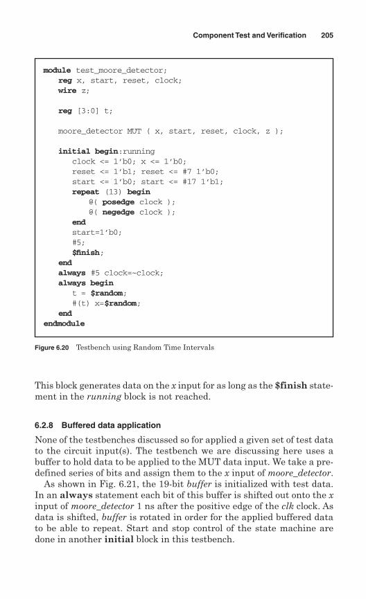
This block generates data on the x input for as long as the $finish state-ment in the running block is not reached.
6.2.8 Buffered data application
None of the testbenches discussed so for applied a given set of test datato the circuit input(s). The testbench we are discussing here uses abuffer to hold data to be applied to the MUT data input. We take a pre-defined series of bits and assign them to the x input of moore_detector.
As shown in Fig. 6.21, the 19-bit buffer is initialized with test data.In an always statement each bit of this buffer is shifted out onto the xinput of moore_detector 1 ns after the positive edge of the clk clock. Asdata is shifted, buffer is rotated in order for the applied buffered datato be able to repeat. Start and stop control of the state machine aredone in another initial block in this testbench.
Component Test and Verification 205
Figure 6.20 Testbench using Random Time Intervals
module test_moore_detector;reg x, start, reset, clock;wire z;
reg [3:0] t;
moore_detector MUT ( x, start, reset, clock, z );
initial begin:runningclock <= 1’b0; x <= 1’b0;reset <= 1’b1; reset <= #7 1’b0; start <= 1’b0; start <= #17 1’b1;repeat (13) begin
@( posedge clock );@( negedge clock );
endstart=1’b0;#5;$finish;
endalways #5 clock=~clock;always begin
t = $random;#(t) x=$random;
endendmodule
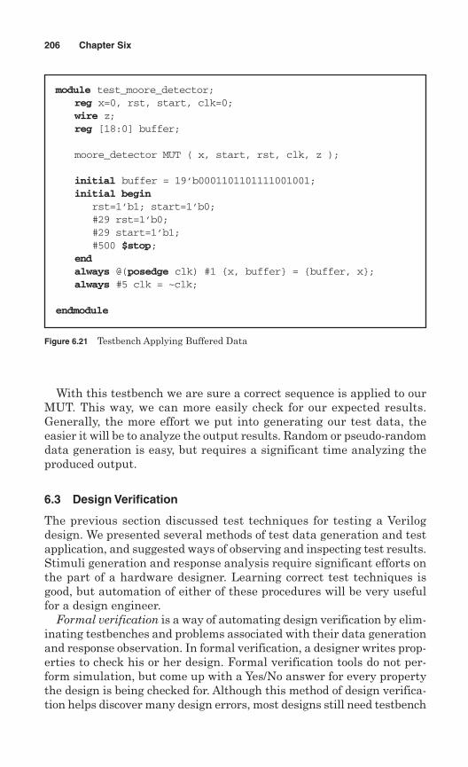
With this testbench we are sure a correct sequence is applied to ourMUT. This way, we can more easily check for our expected results.Generally, the more effort we put into generating our test data, theeasier it will be to analyze the output results. Random or pseudo-randomdata generation is easy, but requires a significant time analyzing theproduced output.
6.3 Design Verification
The previous section discussed test techniques for testing a Verilogdesign. We presented several methods of test data generation and testapplication, and suggested ways of observing and inspecting test results.Stimuli generation and response analysis require significant efforts onthe part of a hardware designer. Learning correct test techniques isgood, but automation of either of these procedures will be very usefulfor a design engineer.
Formal verification is a way of automating design verification by elim-inating testbenches and problems associated with their data generationand response observation. In formal verification, a designer writes prop-erties to check his or her design. Formal verification tools do not per-form simulation, but come up with a Yes/No answer for every propertythe design is being checked for. Although this method of design verifica-tion helps discover many design errors, most designs still need testbench
206 Chapter Six
Figure 6.21 Testbench Applying Buffered Data
module test_moore_detector;reg x=0, rst, start, clk=0;wire z;reg [18:0] buffer;
moore_detector MUT ( x, start, rst, clk, z );
initial buffer = 19’b0001101101111001001;initial begin
rst=1’b1; start=1’b0;#29 rst=1’b0;#29 start=1’b1;#500 $stop;
endalways @(posedge clk) #1 {x, buffer} = {buffer, x};always #5 clk = ~clk;
endmodule
development and simulation for validating that their Verilog code indeedfunctions as expected. In other words, an all “Yes” answers to designproperties checked by formal verification tools is still not enough.
Instead of eliminating data generation and response observation (likethe formal verification tools), a step in the direction of automating designvalidation is to reduce or eliminate efforts needed for analyzing outputresponses. For this purpose assertion verification is used. Assertion ver-ification adds monitors to a design to improve its observability. Whilethe design is being simulated with its testbench data, assertion moni-tors that represent certain design properties continuously check for cor-rect design behavior by validating these properties. If the simulationdata leads into conditions that indicate to an assertion monitor that thedesign is misbehaving, the monitor is said to fire to alert the designerof the problem.
As mentioned, we still need to develop a testbench and careful plan-ning of test inputs for the design being tested is needed in assertion ver-ification. But, in many cases, assertions automatically check to makesure events that occur in the design are as expected. This significantlyreduces the need for processing long output lists or waveforms.
6.4 Assertion Verification
Unlike simulation that a testbench or a human has to interpret theresults, in assertion verification, in-code monitors take the responsibil-ity of issuing a message if something happens that is not expected. InVerilog, these monitors are modules, and they are instantiated in adesign to check for certain design properties. Instantiating an assertionmodule is not to be regarded as instantiation of a hardware module.Instead, this kind of instantiation is more like an always-active proce-dure that continuously checks for events in the design module.
The present set of assertion monitors are available in a library thatis referred to as open verification library (OVL). Designers can developtheir own set of assertions, and use them in their designs. The existingmonitors check for values of signals, relation of several signals witheach other, sequence of events, and expected patterns on vectors orgroups of signals. For using assertions, a designer compiles OVL and hisor her own assertion library into a simulation library and makes thislibrary available to designs being verified. When a design is developed,assertions are placed at key points in the design to check for key func-tionalities. When the design is being simulated as a stand-alone com-ponent, or in a hierarchy of a larger design, the monitors check signalsfor their expected values. If a signal does not have a value expected bya monitor, the assertion monitor displays a message and the time thatthe discrepancy (violation of the property) has occurred. Usually, suchmessages appear in the simulation report area, transcript, or console.
Component Test and Verification 207
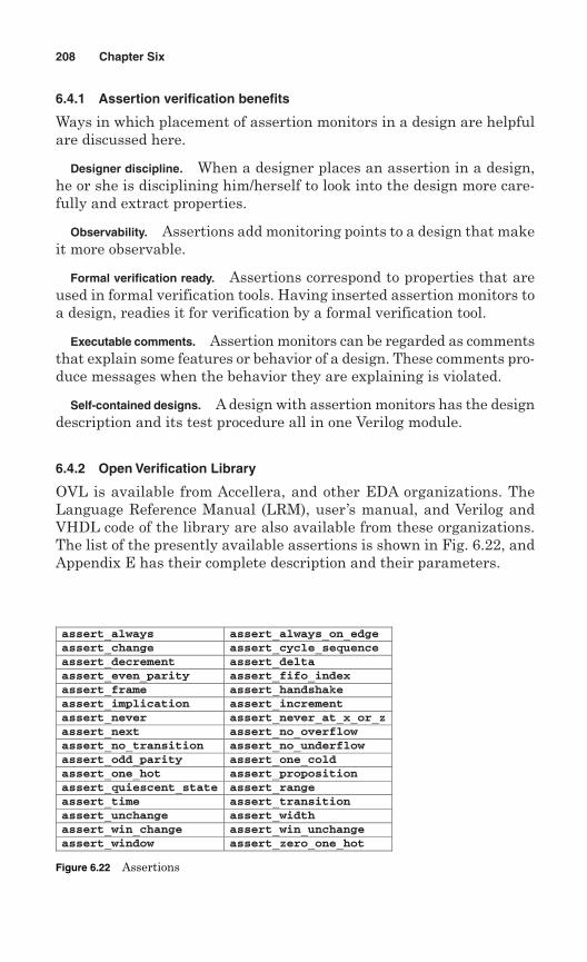
6.4.1 Assertion verification benefits
Ways in which placement of assertion monitors in a design are helpfulare discussed here.
Designer discipline. When a designer places an assertion in a design,he or she is disciplining him/herself to look into the design more care-fully and extract properties.
Observability. Assertions add monitoring points to a design that makeit more observable.
Formal verification ready. Assertions correspond to properties that areused in formal verification tools. Having inserted assertion monitors toa design, readies it for verification by a formal verification tool.
Executable comments. Assertion monitors can be regarded as commentsthat explain some features or behavior of a design. These comments pro-duce messages when the behavior they are explaining is violated.
Self-contained designs. A design with assertion monitors has the designdescription and its test procedure all in one Verilog module.
6.4.2 Open Verification Library
OVL is available from Accellera, and other EDA organizations. TheLanguage Reference Manual (LRM), user’s manual, and Verilog andVHDL code of the library are also available from these organizations.The list of the presently available assertions is shown in Fig. 6.22, andAppendix E has their complete description and their parameters.
208 Chapter Six
assert_always assert_always_on_edge assert_change assert_cycle_sequence assert_decrement assert_delta assert_even_parity assert_fifo_index assert_frame assert_handshake assert_implication assert_increment assert_never assert_never_at_x_or_zassert_next assert_no_overflow assert_no_transition assert_no_underflow assert_odd_parity assert_one_cold assert_one_hot assert_proposition assert_quiescent_state assert_range assert_time assert_transition assert_unchange assert_width assert_win_change assert_win_unchange assert_window assert_zero_one_hot
Figure 6.22 Assertions
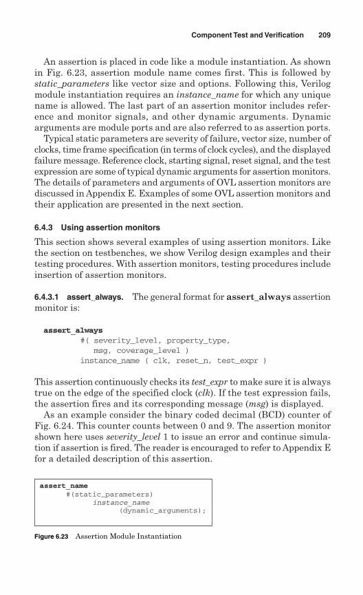
An assertion is placed in code like a module instantiation. As shownin Fig. 6.23, assertion module name comes first. This is followed bystatic_parameters like vector size and options. Following this, Verilogmodule instantiation requires an instance_name for which any uniquename is allowed. The last part of an assertion monitor includes refer-ence and monitor signals, and other dynamic arguments. Dynamicarguments are module ports and are also referred to as assertion ports.
Typical static parameters are severity of failure, vector size, number ofclocks, time frame specification (in terms of clock cycles), and the displayedfailure message. Reference clock, starting signal, reset signal, and the testexpression are some of typical dynamic arguments for assertion monitors.The details of parameters and arguments of OVL assertion monitors arediscussed in Appendix E. Examples of some OVL assertion monitors andtheir application are presented in the next section.
6.4.3 Using assertion monitors
This section shows several examples of using assertion monitors. Likethe section on testbenches, we show Verilog design examples and theirtesting procedures. With assertion monitors, testing procedures includeinsertion of assertion monitors.
6.4.3.1 assert_always. The general format for assert_always assertionmonitor is:
assert_always#( severity_level, property_type,
msg, coverage_level ) instance_name ( clk, reset_n, test_expr )
This assertion continuously checks its test_expr to make sure it is alwaystrue on the edge of the specified clock (clk). If the test expression fails,the assertion fires and its corresponding message (msg) is displayed.
As an example consider the binary coded decimal (BCD) counter ofFig. 6.24. This counter counts between 0 and 9. The assertion monitorshown here uses severity_level 1 to issue an error and continue simula-tion if assertion is fired. The reader is encouraged to refer to Appendix Efor a detailed description of this assertion.
Component Test and Verification 209
assert_name #(static_parameters)
instance_name (dynamic_arguments);
Figure 6.23 Assertion Module Instantiation
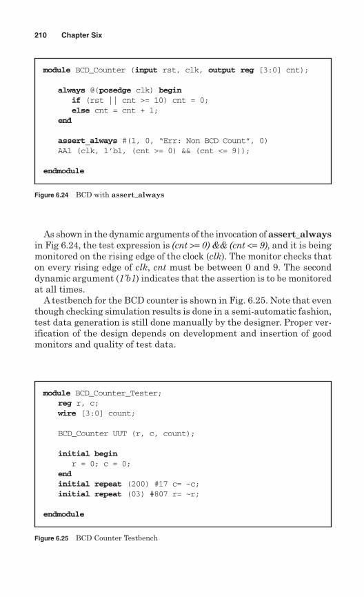
As shown in the dynamic arguments of the invocation of assert_alwaysin Fig 6.24, the test expression is (cnt >= 0) && (cnt <= 9), and it is beingmonitored on the rising edge of the clock (clk). The monitor checks thaton every rising edge of clk, cnt must be between 0 and 9. The seconddynamic argument (1’b1) indicates that the assertion is to be monitoredat all times.
A testbench for the BCD counter is shown in Fig. 6.25. Note that eventhough checking simulation results is done in a semi-automatic fashion,test data generation is still done manually by the designer. Proper ver-ification of the design depends on development and insertion of goodmonitors and quality of test data.
210 Chapter Six
Figure 6.24 BCD with assert_always
module BCD_Counter (input rst, clk, output reg [3:0] cnt);
always @(posedge clk) beginif (rst || cnt >= 10) cnt = 0;else cnt = cnt + 1;
end
assert_always #(1, 0, “Err: Non BCD Count”, 0)AA1 (clk, 1’b1, (cnt >= 0) && (cnt <= 9));
endmodule
Figure 6.25 BCD Counter Testbench
module BCD_Counter_Tester;reg r, c;wire [3:0] count;
BCD_Counter UUT (r, c, count);
initial beginr = 0; c = 0;
endinitial repeat (200) #17 c= ~c;initial repeat (03) #807 r= ~r;
endmodule
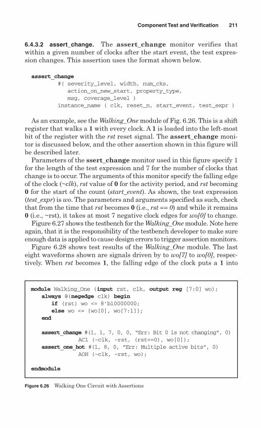
6.4.3.2 assert_change. The assert_change monitor verifies thatwithin a given number of clocks after the start event, the test expres-sion changes. This assertion uses the format shown below.
assert_change#( severity_level, width, num_cks,
action_on_new_start, property_type,msg, coverage_level )
instance_name ( clk, reset_n, start_event, test_expr )
As an example, see the Walking_One module of Fig. 6.26. This is a shiftregister that walks a 1 with every clock. A 1 is loaded into the left-mostbit of the register with the rst reset signal. The assert_change moni-tor is discussed below, and the other assertion shown in this figure willbe described later.
Parameters of the ssert_change monitor used in this figure specify 1for the length of the test expression and 7 for the number of clocks thatchange is to occur. The arguments of this monitor specify the falling edgeof the clock (~clk), rst value of 0 for the activity period, and rst becoming0 for the start of the count (start_event). As shown, the test expression(test_expr) is wo. The parameters and arguments specified as such, checkthat from the time that rst becomes 0 (i.e., rst == 0) and while it remains0 (i.e., ~rst), it takes at most 7 negative clock edges for wo[0] to change.
Figure 6.27 shows the testbench for the Walking_One module. Note hereagain, that it is the responsibility of the testbench developer to make sureenough data is applied to cause design errors to trigger assertion monitors.
Figure 6.28 shows test results of the Walking_One module. The lasteight waveforms shown are signals driven by to wo[7] to wo[0], respec-tively. When rst becomes 1, the falling edge of the clock puts a 1 into
Component Test and Verification 211
Figure 6.26 Walking One Circuit with Assertions
module Walking_One (input rst, clk, output reg [7:0] wo);always @(negedge clk) begin
if (rst) wo <= 8’b10000000;else wo <= {wo[0], wo[7:1]};
end
assert_change #(1, 1, 7, 0, 0, “Err: Bit 0 is not changing”, 0)AC1 (~clk, ~rst, (rst==0), wo[0]);
assert_one_hot #(1, 8, 0, “Err: Multiple active bits”, 0) AOH (~clk, ~rst, wo);
endmodule
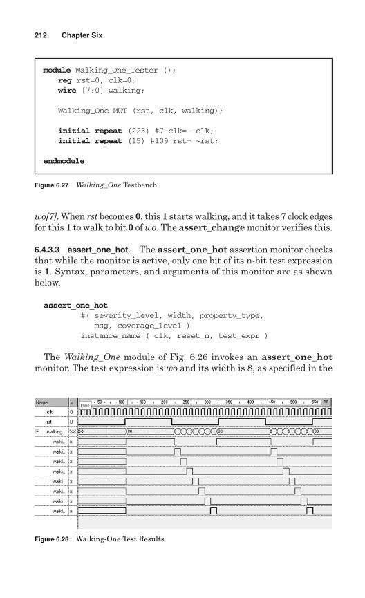
wo[7]. When rst becomes 0, this 1 starts walking, and it takes 7 clock edgesfor this 1 to walk to bit 0 of wo. The assert_change monitor verifies this.
6.4.3.3 assert_one_hot. The assert_one_hot assertion monitor checksthat while the monitor is active, only one bit of its n-bit test expressionis 1. Syntax, parameters, and arguments of this monitor are as shownbelow.
assert_one_hot#( severity_level, width, property_type,
msg, coverage_level ) instance_name ( clk, reset_n, test_expr )
The Walking_One module of Fig. 6.26 invokes an assert_one_hotmonitor. The test expression is wo and its width is 8, as specified in the
212 Chapter Six
Figure 6.27 Walking_One Testbench
module Walking_One_Tester ();reg rst=0, clk=0;wire [7:0] walking;
Walking_One MUT (rst, clk, walking);
initial repeat (223) #7 clk= ~clk;initial repeat (15) #109 rst= ~rst;
endmodule
Figure 6.28 Walking-One Test Results
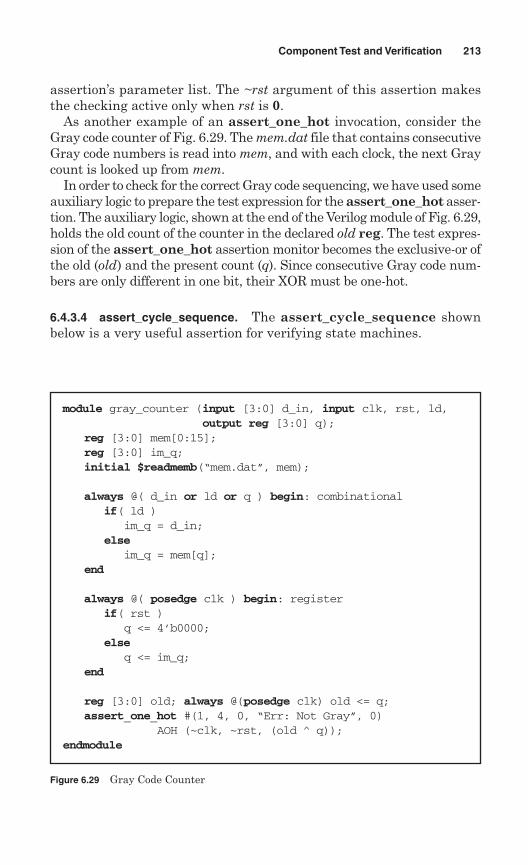
assertion’s parameter list. The ~rst argument of this assertion makesthe checking active only when rst is 0.
As another example of an assert_one_hot invocation, consider theGray code counter of Fig. 6.29. The mem.dat file that contains consecutiveGray code numbers is read into mem, and with each clock, the next Graycount is looked up from mem.
In order to check for the correct Gray code sequencing, we have used someauxiliary logic to prepare the test expression for the assert_one_hot asser-tion. The auxiliary logic, shown at the end of the Verilog module of Fig. 6.29,holds the old count of the counter in the declared old reg. The test expres-sion of the assert_one_hot assertion monitor becomes the exclusive-or ofthe old (old) and the present count (q). Since consecutive Gray code num-bers are only different in one bit, their XOR must be one-hot.
6.4.3.4 assert_cycle_sequence. The assert_cycle_sequence shownbelow is a very useful assertion for verifying state machines.
Component Test and Verification 213
Figure 6.29 Gray Code Counter
module gray_counter (input [3:0] d_in, input clk, rst, ld, output reg [3:0] q);
reg [3:0] mem[0:15];reg [3:0] im_q;initial $readmemb(“mem.dat”, mem);
always @( d_in or ld or q ) begin: combinationalif( ld )
im_q = d_in;else
im_q = mem[q];end
always @( posedge clk ) begin: registerif( rst )
q <= 4’b0000;else
q <= im_q;end
reg [3:0] old; always @(posedge clk) old <= q;assert_one_hot #(1, 4, 0, “Err: Not Gray”, 0)
AOH (~clk, ~rst, (old ^ q));endmodule
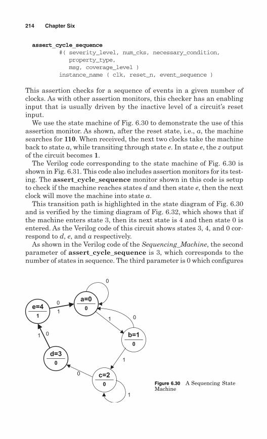
assert_cycle_sequence#( severity_level, num_cks, necessary_condition,
property_type,msg, coverage_level )
instance_name ( clk, reset_n, event_sequence )
This assertion checks for a sequence of events in a given number ofclocks. As with other assertion monitors, this checker has an enablinginput that is usually driven by the inactive level of a circuit’s resetinput.
We use the state machine of Fig. 6.30 to demonstrate the use of thisassertion monitor. As shown, after the reset state, i.e., a, the machinesearches for 110. When received, the next two clocks take the machineback to state a, while transiting through state e. In state e, the z outputof the circuit becomes 1.
The Verilog code corresponding to the state machine of Fig. 6.30 isshown in Fig. 6.31. This code also includes assertion monitors for its test-ing. The assert_cycle_sequence monitor shown in this code is setupto check if the machine reaches states d and then state e, then the nextclock will move the machine into state a.
This transition path is highlighted in the state diagram of Fig. 6.30and is verified by the timing diagram of Fig. 6.32, which shows that ifthe machine enters state 3, then its next state is 4 and then state 0 isentered. As the Verilog code of this circuit shows states 3, 4, and 0 cor-respond to d, e, and a respectively.
As shown in the Verilog code of the Sequencing_Machine, the secondparameter of assert_cycle_sequence is 3, which corresponds to thenumber of states in sequence. The third parameter is 0 which configures
214 Chapter Six
b=10
d=30
c=20
a=00
0
1 0
1
0
1
01
e=41
1
0
Figure 6.30 A Sequencing StateMachine
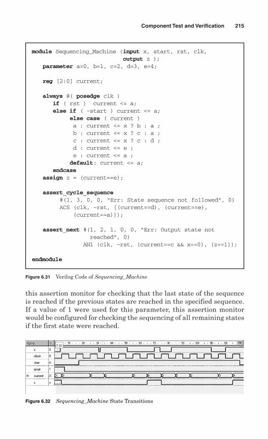
this assertion monitor for checking that the last state of the sequenceis reached if the previous states are reached in the specified sequence.If a value of 1 were used for this parameter, this assertion monitorwould be configured for checking the sequencing of all remaining statesif the first state were reached.
Component Test and Verification 215
Figure 6.31 Verilog Code of Sequencing_Machine
module Sequencing_Machine (input x, start, rst, clk,output z );
parameter a=0, b=1, c=2, d=3, e=4;
reg [2:0] current;
always @( posedge clk )if ( rst ) current <= a;else if ( ~start ) current <= a;
else case ( current )a : current <= x ? b : a ;b : current <= x ? c : a ;c : current <= x ? c : d ;d : current <= e ;e : current <= a ;default: current <= a;
endcaseassign z = (current==e);
assert_cycle_sequence#(1, 3, 0, 0, “Err: State sequence not followed”, 0)ACS (clk, ~rst, {(current==d), (current==e),
(current==a)});
assert_next #(1, 2, 1, 0, 0, “Err: Output state notreached”, 0)
AN1 (clk, ~rst, (current==c && x==0), (z==1));
endmodule
Figure 6.32 Sequencing_Machine State Transitions
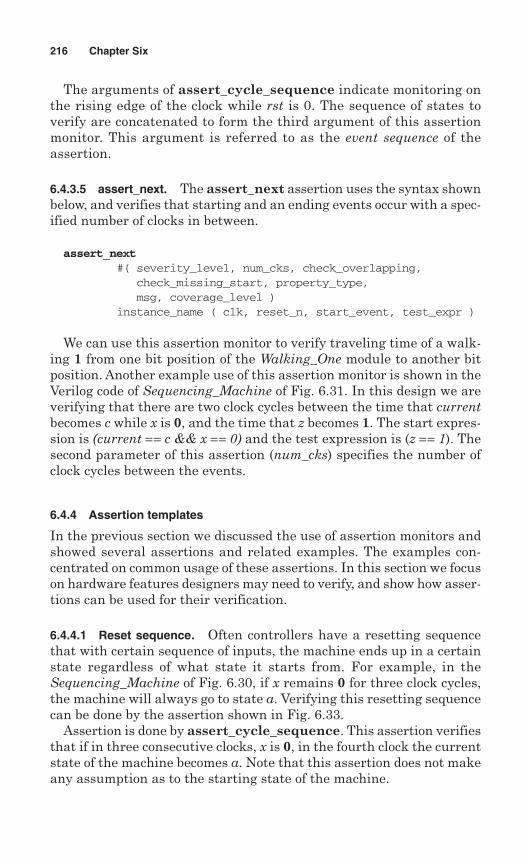
The arguments of assert_cycle_sequence indicate monitoring onthe rising edge of the clock while rst is 0. The sequence of states toverify are concatenated to form the third argument of this assertionmonitor. This argument is referred to as the event sequence of theassertion.
6.4.3.5 assert_next. The assert_next assertion uses the syntax shownbelow, and verifies that starting and an ending events occur with a spec-ified number of clocks in between.
assert_next#( severity_level, num_cks, check_overlapping,
check_missing_start, property_type,msg, coverage_level )
instance_name ( clk, reset_n, start_event, test_expr )
We can use this assertion monitor to verify traveling time of a walk-ing 1 from one bit position of the Walking_One module to another bitposition. Another example use of this assertion monitor is shown in theVerilog code of Sequencing_Machine of Fig. 6.31. In this design we areverifying that there are two clock cycles between the time that currentbecomes c while x is 0, and the time that z becomes 1. The start expres-sion is (current == c && x == 0) and the test expression is (z == 1). Thesecond parameter of this assertion (num_cks) specifies the number ofclock cycles between the events.
6.4.4 Assertion templates
In the previous section we discussed the use of assertion monitors andshowed several assertions and related examples. The examples con-centrated on common usage of these assertions. In this section we focuson hardware features designers may need to verify, and show how asser-tions can be used for their verification.
6.4.4.1 Reset sequence. Often controllers have a resetting sequencethat with certain sequence of inputs, the machine ends up in a certainstate regardless of what state it starts from. For example, in theSequencing_Machine of Fig. 6.30, if x remains 0 for three clock cycles,the machine will always go to state a. Verifying this resetting sequencecan be done by the assertion shown in Fig. 6.33.
Assertion is done by assert_cycle_sequence. This assertion verifiesthat if in three consecutive clocks, x is 0, in the fourth clock the currentstate of the machine becomes a. Note that this assertion does not makeany assumption as to the starting state of the machine.
216 Chapter Six
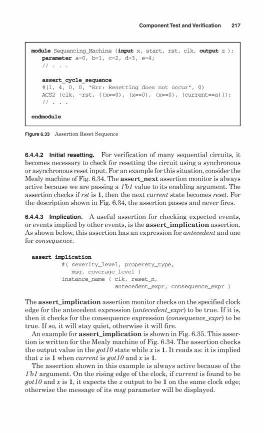
6.4.4.2 Initial resetting. For verification of many sequential circuits, itbecomes necessary to check for resetting the circuit using a synchronousor asynchronous reset input. For an example for this situation, consider theMealy machine of Fig. 6.34. The assert_next assertion monitor is alwaysactive because we are passing a 1’b1 value to its enabling argument. Theassertion checks if rst is 1, then the next current state becomes reset. Forthe description shown in Fig. 6.34, the assertion passes and never fires.
6.4.4.3 Implication. A useful assertion for checking expected events,or events implied by other events, is the assert_implication assertion.As shown below, this assertion has an expression for antecedent and onefor consequence.
assert_implication#( severity_level, properety_type,
msg, coverage_level )instance_name ( clk, reset_n,
antecedent_expr, consequence_expr )
The assert_implication assertion monitor checks on the specified clockedge for the antecedent expression (antecedent_expr) to be true. If it is,then it checks for the consequence expression (consequence_expr) to betrue. If so, it will stay quiet, otherwise it will fire.
An example for assert_implication is shown in Fig. 6.35. This asser-tion is written for the Mealy machine of Fig. 6.34. The assertion checksthe output value in the got10 state while x is 1. It reads as: it is impliedthat z is 1 when current is got10 and x is 1.
The assertion shown in this example is always active because of the1’b1 argument. On the rising edge of the clock, if current is found to begot10 and x is 1, it expects the z output to be 1 on the same clock edge;otherwise the message of its msg parameter will be displayed.
Component Test and Verification 217
Figure 6.33 Assertion Reset Sequence
module Sequencing_Machine (input x, start, rst, clk, output z );parameter a=0, b=1, c=2, d=3, e=4;// . . .
assert_cycle_sequence#(1, 4, 0, 0, “Err: Resetting does not occur”, 0)ACS2 (clk, ~rst, {(x==0), (x==0), (x==0), (current==a)});// . . .
endmodule
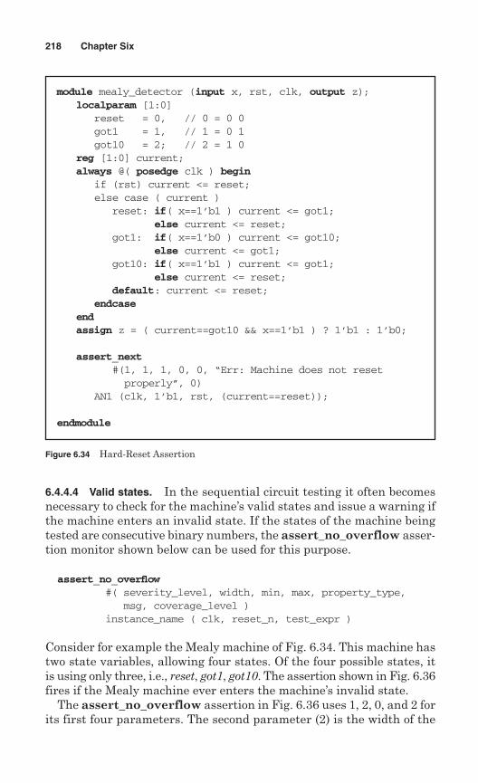
6.4.4.4 Valid states. In the sequential circuit testing it often becomesnecessary to check for the machine’s valid states and issue a warning ifthe machine enters an invalid state. If the states of the machine beingtested are consecutive binary numbers, the assert_no_overflow asser-tion monitor shown below can be used for this purpose.
assert_no_overflow#( severity_level, width, min, max, property_type,
msg, coverage_level ) instance_name ( clk, reset_n, test_expr )
Consider for example the Mealy machine of Fig. 6.34. This machine hastwo state variables, allowing four states. Of the four possible states, itis using only three, i.e., reset, got1, got10. The assertion shown in Fig. 6.36fires if the Mealy machine ever enters the machine’s invalid state.
The assert_no_overflow assertion in Fig. 6.36 uses 1, 2, 0, and 2 forits first four parameters. The second parameter (2) is the width of the
218 Chapter Six
Figure 6.34 Hard-Reset Assertion
module mealy_detector (input x, rst, clk, output z);localparam [1:0]
reset = 0, // 0 = 0 0got1 = 1, // 1 = 0 1got10 = 2; // 2 = 1 0
reg [1:0] current;always @( posedge clk ) begin
if (rst) current <= reset;else case ( current )
reset: if( x==1’b1 ) current <= got1;else current <= reset;
got1: if( x==1’b0 ) current <= got10;else current <= got1;
got10: if( x==1’b1 ) current <= got1;else current <= reset;
default: current <= reset;endcase
endassign z = ( current==got10 && x==1’b1 ) ? 1’b1 : 1’b0;
assert_next#(1, 1, 1, 0, 0, “Err: Machine does not resetproperly”, 0)
AN1 (clk, 1’b1, rst, (current==reset));
endmodule
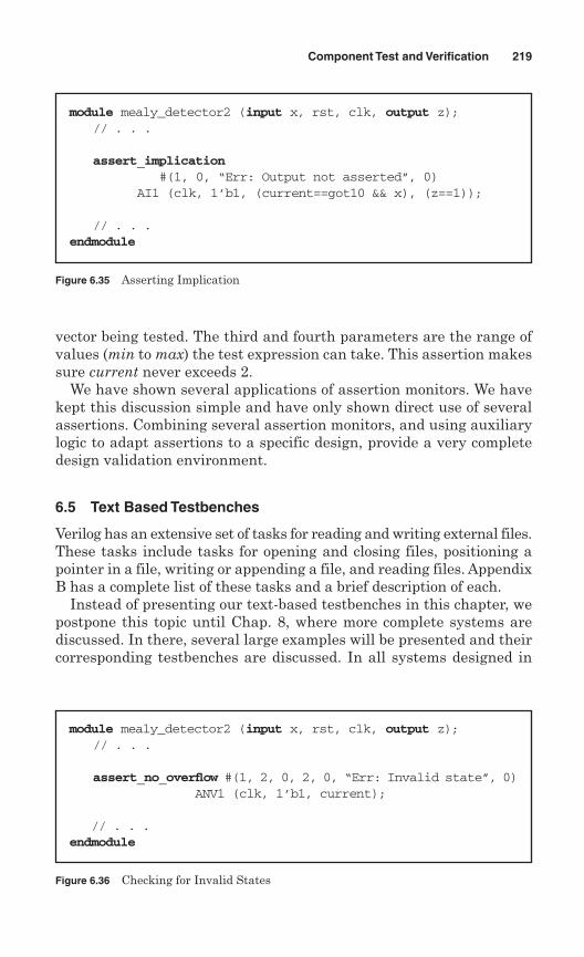
vector being tested. The third and fourth parameters are the range ofvalues (min to max) the test expression can take. This assertion makessure current never exceeds 2.
We have shown several applications of assertion monitors. We havekept this discussion simple and have only shown direct use of severalassertions. Combining several assertion monitors, and using auxiliarylogic to adapt assertions to a specific design, provide a very completedesign validation environment.
6.5 Text Based Testbenches
Verilog has an extensive set of tasks for reading and writing external files.These tasks include tasks for opening and closing files, positioning apointer in a file, writing or appending a file, and reading files. AppendixB has a complete list of these tasks and a brief description of each.
Instead of presenting our text-based testbenches in this chapter, wepostpone this topic until Chap. 8, where more complete systems arediscussed. In there, several large examples will be presented and theircorresponding testbenches are discussed. In all systems designed in
Component Test and Verification 219
Figure 6.35 Asserting Implication
module mealy_detector2 (input x, rst, clk, output z);// . . .
assert_implication#(1, 0, “Err: Output not asserted”, 0)
AI1 (clk, 1’b1, (current==got10 && x), (z==1));
// . . .endmodule
Figure 6.36 Checking for Invalid States
module mealy_detector2 (input x, rst, clk, output z);// . . .
assert_no_overflow #(1, 2, 0, 2, 0, “Err: Invalid state”, 0)ANV1 (clk, 1’b1, current);
// . . .endmodule
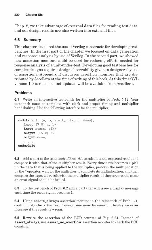
Chap. 8, we take advantage of external data files for reading test data,and our design results are also written into external files.
6.6 Summary
This chapter discussed the use of Verilog constructs for developing test-benches. In the first part of the chapter we focused on data generationand response analysis by use of Verilog. In the second part, we showedhow assertion monitors could be used for reducing efforts needed forresponse analysis of a unit-under-test. Developing good testbenches forcomplex designs requires design observability given to designers by useof assertions. Appendix E discusses assertion monitors that are dis-tributed by Accellera at the time of writing of this book. At this time OVLversion 1.0 is released and updates will be available from Accellera.
Problems
6.1 Write an interactive testbench for the multiplier of Prob. 5.12. Yourtestbench must be complete with clock and proper timing and multiplierhandshaking. Use the following interface for the multiplier,
6.2 Add a part to the testbench of Prob. 6.1 to calculate the expected result andcompare it with that of the multiplier result. Every time start becomes 1 pickup the data that is being applied to the multiplier, perform the multiplicationby the * operator, wait for the multiplier to complete its multiplication, and thencompare the expected result with the multiplier result. If they are not the samean error signal should be issued.
6.3 To the testbench of Prob. 6.2 add a part that will issue a display messageeach time the error signal becomes 1.
6.4 Using assert_always assertion monitor in the testbench of Prob. 6.1,continuously check the result every time done becomes 1. Display an errormessage if the result is wrong.
6.5 Rewrite the assertion of the BCD counter of Fig. 6.24. Instead ofassert_always, use assert_no_overflow assertion monitor to check the BCDcounting.
220 Chapter Six
module mult (a, b, start, clk, r, done);input [7:0] a, b;input start, clk;output [15:0] r;output done;. . .
endmodule
Suggested Reading
Accellera, Open Verification Library: Assertion Monitor Reference Manual, www.accellera.org, v1.0, 2005.
Bening, L., and H.D. Foster, Principles of Verifiable RTL Design Second Edition–AFunctional Coding Style Supporting Verification Processes in Verilog, 2d ed. Springer,Boston, 2001, ISBN: 0792373685.
Foster, H.D., A.C. Krolnik, and D.J. Lacey, Assertion-Based Design, 1st ed. Springer,Boston, 2003, ISBN: 1402074980.
IEEE Std 1364-2001, IEEE Standard Verilog Language Reference Manual, SH94921-TBR (print) SS94921-TBR (electronic), ISBN 0-7381-2827-9 (print and electronic),2001.
Lam, W. K., Hardware Design Verification: Simulation and Formal Method-BasedApproaches, Prentice Hall PTR, New Jersey, 2005, ISBN: 0131433474.
Navabi, Z., Digital Design and Implementation with Field Programmable Devices, KluwerAcademic Publishers, Boston, 2005, ISBN: 1-4020-8011-5.
Navabi, Z., Verilog Computer-Based Training Course, CBT CD with hardcopy User’smanual, McGraw-Hill, New York, 2002, ISBN 0-07-137473-6.
Component Test and Verification 221

This page intentionally left blank
Chapter
7Detailed Modeling
The previous chapters presented Verilog from a design point of view.Except in a few cases, most of the constructs and styles of coding thatwe discussed were synthesizable. Although describing hardware for syn-thesis covers the majority of cases that a hardware description language(HDL) like Verilog is used in industry, there are also cases that an exist-ing hardware needs to be modeled. Take for example, developing com-ponents of an application-specific integrated circuits (ASIC) library forpost-synthesis simulation, or modeling very large-scale integration(VLSI) components to be used in a hierarchical multi-level design descrip-tion. In such cases, there may be a need to go beyond gate level detailsof a structure and develop models to exhibit timing signal strengths,and signal values that are less abstract than just 0 and 1.
There are two facilities in Verilog for detailed modeling beyond whatwe have already discussed: transistor (or switch) level modeling andsignal strengths. These facilities are independent, but can be combinedto facilitate modeling hardware for a very detailed simulation. Thischapter presents switch level modeling and signal strengths in Verilog.We show simulation results that can be obtained by hardware modelsthat take advantage of such language facilities.
7.1 Switch Level Modeling
Usually, transistor level modeling is referred to modeling hardwarestructures using transistor models with analog input and output signalvalues. On the other hand, gate level modeling refers to modeling hard-ware structures using gate models with digital input and output signalvalues. Between these two modeling schemes is what is referred to asswitch level modeling. At this level, a hardware component is described
223
Copyright © 2006 by The McGraw-Hill Publishing Companies, Inc. Click here for terms of use.
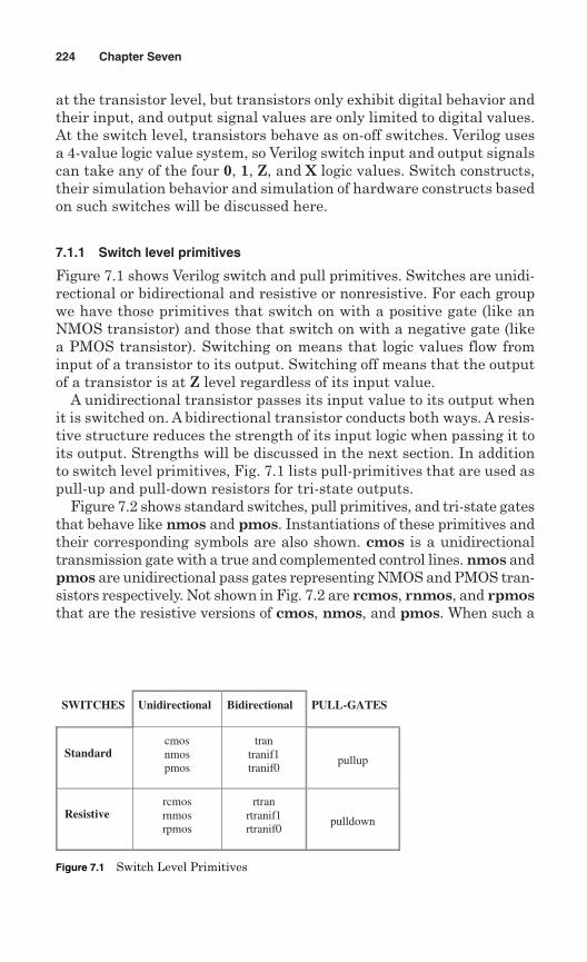
at the transistor level, but transistors only exhibit digital behavior andtheir input, and output signal values are only limited to digital values.At the switch level, transistors behave as on-off switches. Verilog usesa 4-value logic value system, so Verilog switch input and output signalscan take any of the four 0, 1, Z, and X logic values. Switch constructs,their simulation behavior and simulation of hardware constructs basedon such switches will be discussed here.
7.1.1 Switch level primitives
Figure 7.1 shows Verilog switch and pull primitives. Switches are unidi-rectional or bidirectional and resistive or nonresistive. For each groupwe have those primitives that switch on with a positive gate (like anNMOS transistor) and those that switch on with a negative gate (likea PMOS transistor). Switching on means that logic values flow frominput of a transistor to its output. Switching off means that the outputof a transistor is at Z level regardless of its input value.
A unidirectional transistor passes its input value to its output whenit is switched on. A bidirectional transistor conducts both ways. A resis-tive structure reduces the strength of its input logic when passing it toits output. Strengths will be discussed in the next section. In additionto switch level primitives, Fig. 7.1 lists pull-primitives that are used aspull-up and pull-down resistors for tri-state outputs.
Figure 7.2 shows standard switches, pull primitives, and tri-state gatesthat behave like nmos and pmos. Instantiations of these primitives andtheir corresponding symbols are also shown. cmos is a unidirectionaltransmission gate with a true and complemented control lines. nmos andpmos are unidirectional pass gates representing NMOS and PMOS tran-sistors respectively. Not shown in Fig. 7.2 are rcmos, rnmos, and rpmosthat are the resistive versions of cmos, nmos, and pmos. When such a
224 Chapter Seven
SWITCHES Unidirectional Bidirectional PULL-GATES
Standardcmosnmospmos
trantranif1tranif0
pullup
Resistivercmosrnmosrpmos
rtranrtranif1rtranif0
pulldown
Figure 7.1 Switch Level Primitives
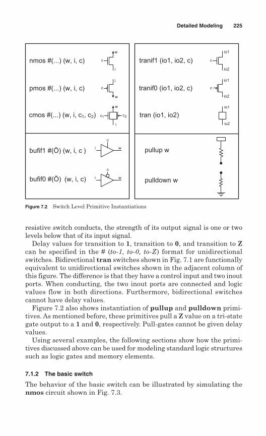
resistive switch conducts, the strength of its output signal is one or twolevels below that of its input signal.
Delay values for transition to 1, transition to 0, and transition to Zcan be specified in the # (to-1, to-0, to-Z) format for unidirectionalswitches. Bidirectional tran switches shown in Fig. 7.1 are functionallyequivalent to unidirectional switches shown in the adjacent column ofthis figure. The difference is that they have a control input and two inoutports. When conducting, the two inout ports are connected and logicvalues flow in both directions. Furthermore, bidirectional switchescannot have delay values.
Figure 7.2 also shows instantiation of pullup and pulldown primi-tives. As mentioned before, these primitives pull a Z value on a tri-stategate output to a 1 and 0, respectively. Pull-gates cannot be given delayvalues.
Using several examples, the following sections show how the primi-tives discussed above can be used for modeling standard logic structuressuch as logic gates and memory elements.
7.1.2 The basic switch
The behavior of the basic switch can be illustrated by simulating thenmos circuit shown in Fig. 7.3.
Detailed Modeling 225
Figure 7.2 Switch Level Primitive Instantiations
nmos #(...) (w, i, c)
pmos #(...) (w, i, c)
w
c
w
i
c
w
i
i
cmos #(...) (w, i, c1, c2) c1 c2
tranif1 (io1, io2, c)
tranif0 (io1, io2, c)
io1
c
io2
io1
c
io1
io2
io2
tran (io1, io2)
bufif1 #(Ö) (w, i, c )
bufif0 #(Ö) (w, i, c)
c
c
i
i
w
w
pullup w
pulldown w
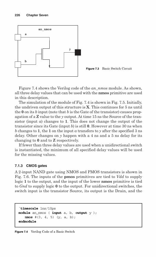
Figure 7.4 shows the Verilog code of the an_nmos module. As shown,all three delay values that can be used with the nmos primitive are usedin this description.
The simulation of the module of Fig. 7.4 is shown in Fig. 7.5. Initially,the undriven output of this structure is X. This continues for 5 ns untilthe 0 on its b input (note that b is the Gate of the transistor) causes prop-agation of a Z value to the y output. At time 15 ns the Source of the tran-sistor (input a) changes to 1. This does not change the output of thetransistor since its Gate (input b) is still 0. However at time 30 ns whenb changes to 1, the 1 on the input a transfers to y after the specified 3 nsdelay. Other changes on y happen with a 4 ns and a 5 ns delay for itschanging to 0 and to Z respectively.
If fewer than three delay values are used when a unidirectional switchis instantiated, the minimum of all specified delay values will be usedfor the missing values.
7.1.3 CMOS gates
A 2-input NAND gate using NMOS and PMOS transistors is shown inFig. 7.6. The inputs of the pmos primitives are tied to Vdd to supplylogic 1 to the output, and the input of the lower nmos primitive is tiedto Gnd to supply logic 0 to the output. For unidirectional switches, theswitch input is the transistor Source, its output is the Drain, and the
226 Chapter Seven
a
b
y
an_nmos
Figure 7.3 Basic Switch Circuit
Figure 7.4 Verilog Code of a Basic Switch
`timescale 1ns/10psmodule an_nmos ( input a, b, output y );
nmos #(3, 4, 5) (y, a, b);endmodule
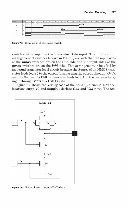
switch control input is the transistor Gate input. The input-outputarrangement of switches (shown in Fig. 7.6) are such that the input sidesof the nmos switches are on the Gnd side and the input sides of thepmos switches are on the Vdd side. This arrangement is justified byan actual transistor level circuit because the Source of an NMOS tran-sistor feeds logic 0 to the output (discharging the output throught Gnd),and the Source of a PMOS transistor feeds logic 1 to the output (charg-ing it through Vdd) of a CMOS gate.
Figure 7.7 shows the Verilog code of the nand2_1d circuit. Net dec-larations supply0 and supply1 declare Gnd and Vdd nets. The im1
Detailed Modeling 227
Figure 7.5 Simulation of the Basic Switch
nand2_1d
g3
g4
g1 g2a
b
Vdd
Gnd
y
im1
Figure 7.6 Switch Level 2-input NAND Gate
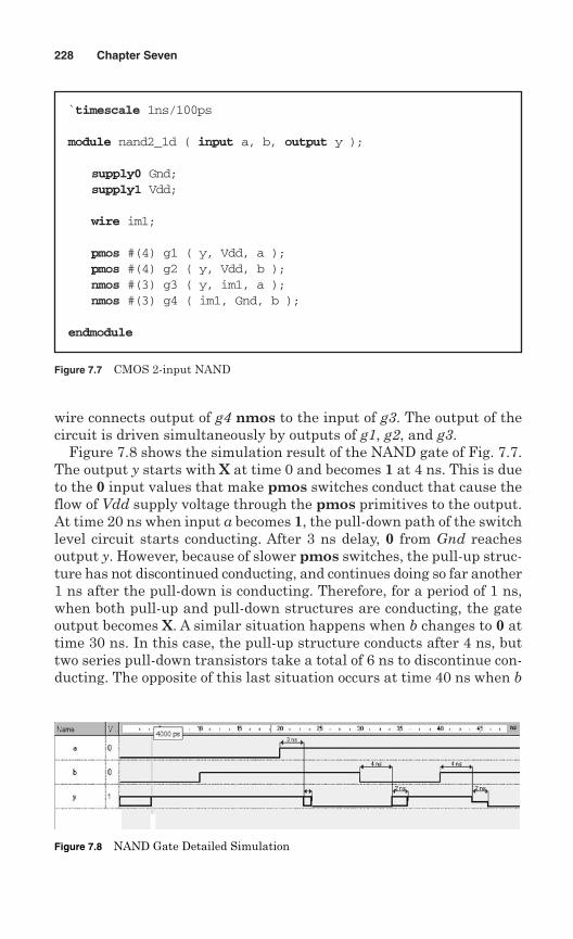
wire connects output of g4 nmos to the input of g3. The output of thecircuit is driven simultaneously by outputs of g1, g2, and g3.
Figure 7.8 shows the simulation result of the NAND gate of Fig. 7.7.The output y starts with X at time 0 and becomes 1 at 4 ns. This is dueto the 0 input values that make pmos switches conduct that cause theflow of Vdd supply voltage through the pmos primitives to the output.At time 20 ns when input a becomes 1, the pull-down path of the switchlevel circuit starts conducting. After 3 ns delay, 0 from Gnd reachesoutput y. However, because of slower pmos switches, the pull-up struc-ture has not discontinued conducting, and continues doing so far another1 ns after the pull-down is conducting. Therefore, for a period of 1 ns,when both pull-up and pull-down structures are conducting, the gateoutput becomes X. A similar situation happens when b changes to 0 attime 30 ns. In this case, the pull-up structure conducts after 4 ns, buttwo series pull-down transistors take a total of 6 ns to discontinue con-ducting. The opposite of this last situation occurs at time 40 ns when b
228 Chapter Seven
Figure 7.7 CMOS 2-input NAND
`timescale 1ns/100ps
module nand2_1d ( input a, b, output y );
supply0 Gnd;supply1 Vdd;
wire im1;
pmos #(4) g1 ( y, Vdd, a );pmos #(4) g2 ( y, Vdd, b );nmos #(3) g3 ( y, im1, a );nmos #(3) g4 ( im1, Gnd, b );
endmodule
Figure 7.8 NAND Gate Detailed Simulation
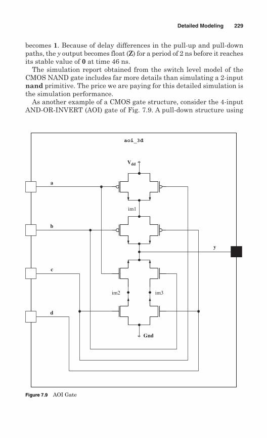
becomes 1. Because of delay differences in the pull-up and pull-downpaths, the y output becomes float (Z) for a period of 2 ns before it reachesits stable value of 0 at time 46 ns.
The simulation report obtained from the switch level model of theCMOS NAND gate includes far more details than simulating a 2-inputnand primitive. The price we are paying for this detailed simulation isthe simulation performance.
As another example of a CMOS gate structure, consider the 4-inputAND-OR-INVERT (AOI) gate of Fig. 7.9. A pull-down structure using
Detailed Modeling 229
a
b
aoi_3d
y
c
d
im3im2
Gnd
Vdd
im1
Figure 7.9 AOI Gate
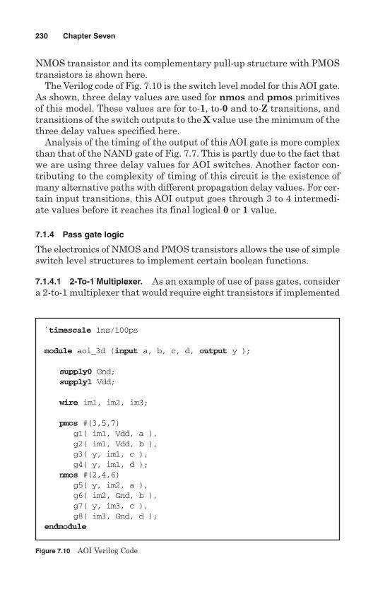
NMOS transistor and its complementary pull-up structure with PMOStransistors is shown here.
The Verilog code of Fig. 7.10 is the switch level model for this AOI gate.As shown, three delay values are used for nmos and pmos primitivesof this model. These values are for to-1, to-0 and to-Z transitions, andtransitions of the switch outputs to the X value use the minimum of thethree delay values specified here.
Analysis of the timing of the output of this AOI gate is more complexthan that of the NAND gate of Fig. 7.7. This is partly due to the fact thatwe are using three delay values for AOI switches. Another factor con-tributing to the complexity of timing of this circuit is the existence ofmany alternative paths with different propagation delay values. For cer-tain input transitions, this AOI output goes through 3 to 4 intermedi-ate values before it reaches its final logical 0 or 1 value.
7.1.4 Pass gate logic
The electronics of NMOS and PMOS transistors allows the use of simpleswitch level structures to implement certain boolean functions.
7.1.4.1 2-To-1 Multiplexer. As an example of use of pass gates, considera 2-to-1 multiplexer that would require eight transistors if implemented
230 Chapter Seven
Figure 7.10 AOI Verilog Code
`timescale 1ns/100ps
module aoi_3d (input a, b, c, d, output y );
supply0 Gnd;supply1 Vdd;
wire im1, im2, im3;
pmos #(3,5,7)g1( im1, Vdd, a ),g2( im1, Vdd, b ),g3( y, im1, c ),g4( y, im1, d );
nmos #(2,4,6)g5( y, im2, a ),g6( im2, Gnd, b ),g7( y, im3, c ),g8( im3, Gnd, d );
endmodule
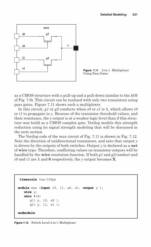
as a CMOS structure with a pull-up and a pull-down (similar to the AOIof Fig. 7.9). This circuit can be realized with only two transistors usingpass gates. Figure 7.11 shows such a multiplexer.
In this circuit, g1 or g2 conducts when s0 or s1 is 1, which allows i0or i1 to propagate to y. Because of the transistor threshold values, andtheir resistance, the y output is at a weaker logic level than if this struc-ture was build as a CMOS complex gate. Verilog models this strengthreduction using its signal strength modeling that will be discussed inthe next section.
The Verilog code of the mux circuit of Fig. 7.11 is shown in Fig. 7.12.Note the direction of unidirectional transistors, and note that output yis driven by the outputs of both switches. Output y is declared as a netof wire type. Therefore, conflicting values on transistor outputs will behandled by the wire resolution function. If both g1 and g2 conduct andi0 and i1 are 1 and 0 respectively, the y output becomes X.
Detailed Modeling 231
g1i0
i1
mux
ys0
s1
g2
Figure 7.11 2-to-1 MultiplexerUsing Pass Gates
Figure 7.12 Switch Level 2-to-1 Multiplexer
`timescale 1ns/100ps
module mux (input i0, i1, s0, s1, output y );wire y;nmos #(4)
g1( y, i0, s0 ),g2( y, i1, s1 );
endmodule
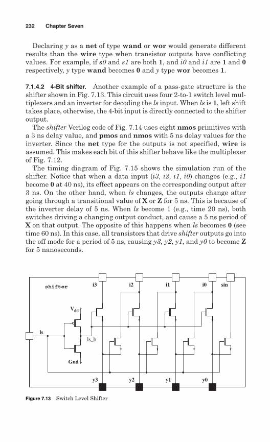
Declaring y as a net of type wand or wor would generate differentresults than the wire type when transistor outputs have conflictingvalues. For example, if s0 and s1 are both 1, and i0 and i1 are 1 and 0respectively, y type wand becomes 0 and y type wor becomes 1.
7.1.4.2 4-Bit shifter. Another example of a pass-gate structure is theshifter shown in Fig. 7.13. This circuit uses four 2-to-1 switch level mul-tiplexers and an inverter for decoding the ls input. When ls is 1, left shifttakes place, otherwise, the 4-bit input is directly connected to the shifteroutput.
The shifter Verilog code of Fig. 7.14 uses eight nmos primitives witha 3 ns delay value, and pmos and nmos with 5 ns delay values for theinverter. Since the net type for the outputs is not specified, wire isassumed. This makes each bit of this shifter behave like the multiplexerof Fig. 7.12.
The timing diagram of Fig. 7.15 shows the simulation run of theshifter. Notice that when a data input (i3, i2, i1, i0) changes (e.g., i1become 0 at 40 ns), its effect appears on the corresponding output after3 ns. On the other hand, when ls changes, the outputs change aftergoing through a transitional value of X or Z for 5 ns. This is because ofthe inverter delay of 5 ns. When ls become 1 (e.g., time 20 ns), bothswitches driving a changing output conduct, and cause a 5 ns period ofX on that output. The opposite of this happens when ls becomes 0 (seetime 60 ns). In this case, all transistors that drive shifter outputs go intothe off mode for a period of 5 ns, causing y3, y2, y1, and y0 to become Zfor 5 nanoseconds.
232 Chapter Seven
shifter i0i1i2i3
ls
sin
y0y1y2y3
ls_b
Vdd
Gnd
Figure 7.13 Switch Level Shifter
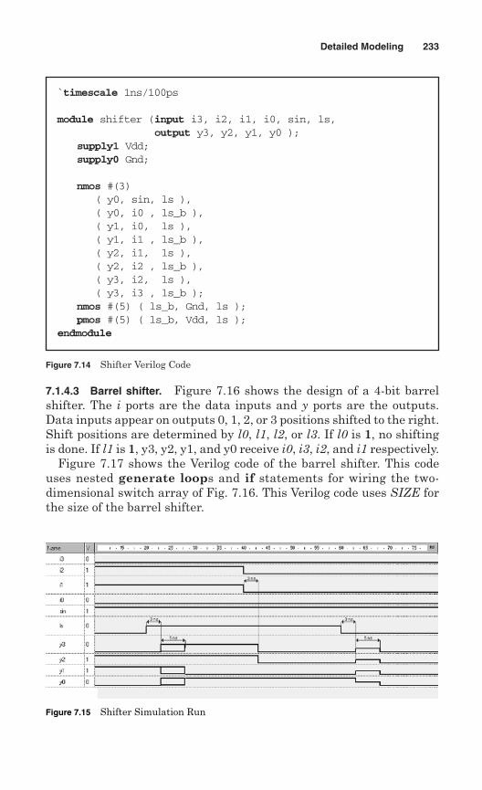
7.1.4.3 Barrel shifter. Figure 7.16 shows the design of a 4-bit barrelshifter. The i ports are the data inputs and y ports are the outputs.Data inputs appear on outputs 0, 1, 2, or 3 positions shifted to the right.Shift positions are determined by l0, l1, l2, or l3. If l0 is 1, no shiftingis done. If l1 is 1, y3, y2, y1, and y0 receive i0, i3, i2, and i1 respectively.
Figure 7.17 shows the Verilog code of the barrel shifter. This codeuses nested generate loops and if statements for wiring the two-dimensional switch array of Fig. 7.16. This Verilog code uses SIZE forthe size of the barrel shifter.
Detailed Modeling 233
Figure 7.14 Shifter Verilog Code
`timescale 1ns/100ps
module shifter (input i3, i2, i1, i0, sin, ls, output y3, y2, y1, y0 );
supply1 Vdd;supply0 Gnd;
nmos #(3)( y0, sin, ls ),( y0, i0 , ls_b ),( y1, i0, ls ),( y1, i1 , ls_b ),( y2, i1, ls ),( y2, i2 , ls_b ),( y3, i2, ls ),( y3, i3 , ls_b );
nmos #(5) ( ls_b, Gnd, ls );pmos #(5) ( ls_b, Vdd, ls );
endmodule
Figure 7.15 Shifter Simulation Run
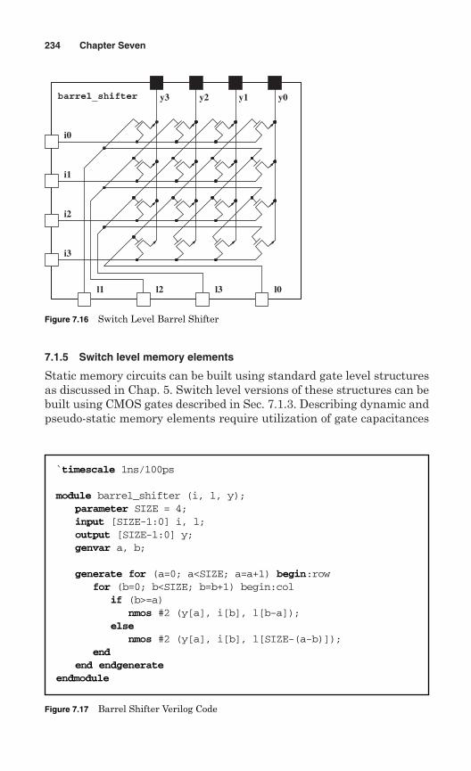
7.1.5 Switch level memory elements
Static memory circuits can be built using standard gate level structuresas discussed in Chap. 5. Switch level versions of these structures can bebuilt using CMOS gates described in Sec. 7.1.3. Describing dynamic andpseudo-static memory elements require utilization of gate capacitances
234 Chapter Seven
i1
barrel_shifter y3 y2 y1 y0
i0
i2
i3
l1 l2 l3 l0
Figure 7.16 Switch Level Barrel Shifter
Figure 7.17 Barrel Shifter Verilog Code
`timescale 1ns/100ps
module barrel_shifter (i, l, y);parameter SIZE = 4;input [SIZE-1:0] i, l;output [SIZE-1:0] y;genvar a, b;
generate for (a=0; a<SIZE; a=a+1) begin:rowfor (b=0; b<SIZE; b=b+1) begin:col
if (b>=a)nmos #2 (y[a], i[b], l[b-a]);
elsenmos #2 (y[a], i[b], l[SIZE-(a-b)]);
endend endgenerate
endmodule
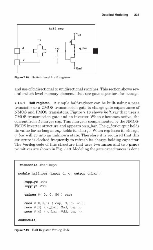
and use of bidirectional or unidirectional switches. This section shows sev-eral switch level memory elements that use gate capacitors for storage.
7.1.5.1 Half register. A simple half-register can be built using a passtransistor or a CMOS transmission gate to charge gate capacitance ofNMOS and PMOS transistors. Figure 7.18 shows half_reg that uses aCMOS transmission gate and an inverter. When c becomes active, thecurrent from d charges cap. This charge is complemented by the NMOS-PMOS inverter structure and appears on q_bar. The q_bar output holdsits value for as long as cap holds its charge. When cap loses its charge,q_bar will go into an unknown state. Therefore it is required that thisstructure is clocked frequently to refresh its charge holding capacitor.The Verilog code of this structure that uses two nmos and two pmosprimitives are shown in Fig. 7.19. Modeling the gate capacitances is done
Detailed Modeling 235
d
half_reg
c
q_barcap
~c
Vdd
Gnd
Figure 7.18 Switch Level Half-Register
Figure 7.19 Half Register Verilog Code
`timescale 1ns/100ps
module half_reg (input d, c, output q_bar);
supply0 Gnd;supply1 Vdd;
trireg #( 0, 0, 50 ) cap;
cmos #(0,0,5) ( cap, d, c, ~c );nmos #(3) ( q_bar, Gnd, cap );pmos #(4) ( q_bar, Vdd, cap );
endmodule
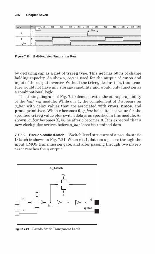
by declaring cap as a net of trireg type. This net has 50 ns of chargeholding capacity. As shown, cap is used for the output of cmos andinput of the output inverter. Without the trireg declaration, this struc-ture would not have any storage capability and would only function asa combinational logic.
The timing diagram of Fig. 7.20 demonstrates the storage capabilityof the half_reg module. While c is 1, the complement of d appears onq_bar with delay values that are associated with cmos, nmos, andpmos primitives. When c becomes 0, q_bar holds its last value for thespecified trireg value plus switch delays as specified in this module. Asshown, q_bar becomes X, 58 ns after c becomes 0. It is expected that anew clock pulse arrives before q_bar loses its retained data.
7.1.5.2 Pseudo-static d-latch. Switch level structure of a pseudo-staticD-latch is shown in Fig. 7.21. When c is 1, data on d passes through theinput CMOS transmission gate, and after passing through two invert-ers it reaches the q output.
236 Chapter Seven
Figure 7.20 Half-Register Simulation Run
d
d_latch
c
q
im1
~c
c~c
q_not
Figure 7.21 Pseudo-Static Transparent Latch
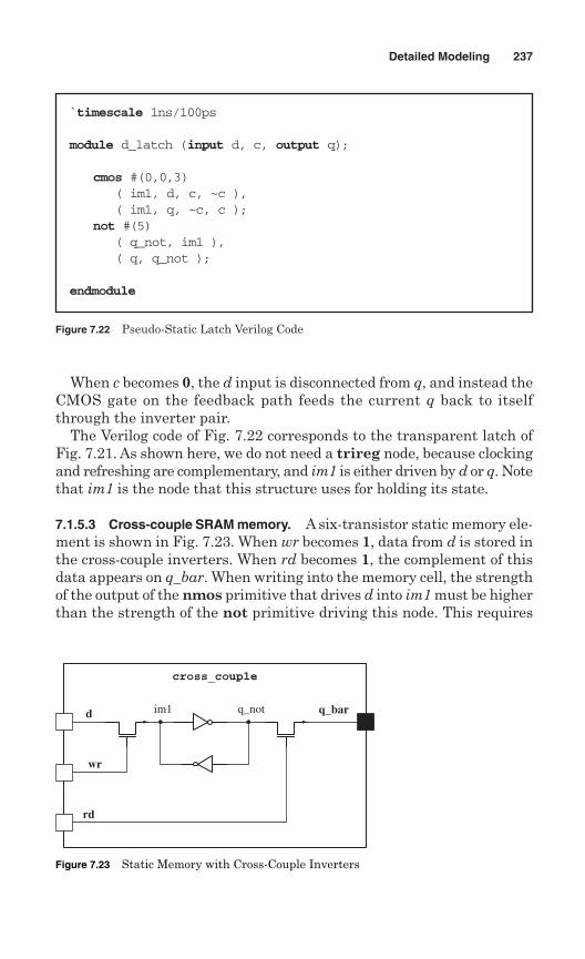
When c becomes 0, the d input is disconnected from q, and instead theCMOS gate on the feedback path feeds the current q back to itselfthrough the inverter pair.
The Verilog code of Fig. 7.22 corresponds to the transparent latch ofFig. 7.21. As shown here, we do not need a trireg node, because clockingand refreshing are complementary, and im1 is either driven by d or q. Notethat im1 is the node that this structure uses for holding its state.
7.1.5.3 Cross-couple SRAM memory. A six-transistor static memory ele-ment is shown in Fig. 7.23. When wr becomes 1, data from d is stored inthe cross-couple inverters. When rd becomes 1, the complement of thisdata appears on q_bar. When writing into the memory cell, the strengthof the output of the nmos primitive that drives d into im1 must be higherthan the strength of the not primitive driving this node. This requires
Detailed Modeling 237
Figure 7.22 Pseudo-Static Latch Verilog Code
`timescale 1ns/100ps
module d_latch (input d, c, output q);
cmos #(0,0,3)( im1, d, c, ~c ),( im1, q, ~c, c );
not #(5)( q_not, im1 ),( q, q_not );
endmodule
d
cross_couple
wr
q_notim1 q_bar
rd
Figure 7.23 Static Memory with Cross-Couple Inverters
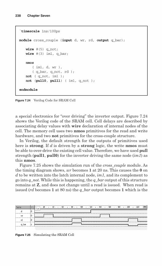
a special electronics for “over driving” the inverter output. Figure 7.24shows the Verilog code of the SRAM cell. Cell delays are described byassociating delay values with wire declaration of internal nodes of thecell. The memory cell uses two nmos primitives for the read and writehardware, and two not primitives for the cross-couple structure.
In Verilog, the default strength for the outputs of primitives usedhere is strong. If d is driven by a strong logic, the write nmos mustbe able to over-drive the existing cell value. Therefore, we have used pullstrength (pull1, pull0) for the inverter driving the same node (im1) asthis nmos.
Figure 7.25 shows the simulation run of the cross_couple module. Asthe timing diagram shows, wr becomes 1 at 20 ns. This causes the 0 ond to be written into the latch internal node, im1, and its complement togo into q_not. While this is happening, the q_bar output of this structureremains at Z, and does not change until a read is issued. When read isissued (rd becomes 1 at 80 ns) the q_bar output becomes 1 which is the
238 Chapter Seven
Figure 7.24 Verilog Code for SRAM Cell
`timescale 1ns/100ps
module cross_couple (input d, wr, rd, output q_bar);
wire #(5) q_not;wire #(3) im1, q_bar;
nmos( im1, d, wr ),( q_bar, q_not, rd );
not ( q_not, im1 );not (pull0, pull1) ( im1, q_not );
endmodule
Figure 7.25 Simulating the SRAM Cell
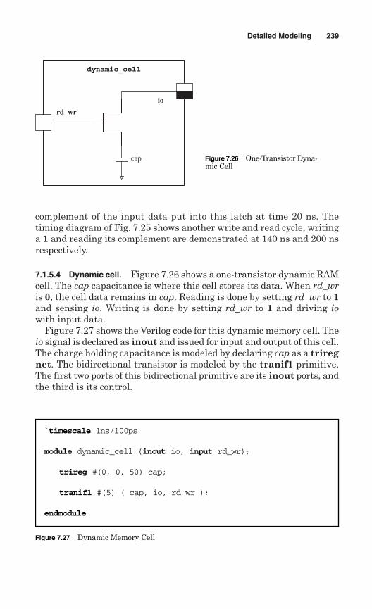
complement of the input data put into this latch at time 20 ns. Thetiming diagram of Fig. 7.25 shows another write and read cycle; writinga 1 and reading its complement are demonstrated at 140 ns and 200 nsrespectively.
7.1.5.4 Dynamic cell. Figure 7.26 shows a one-transistor dynamic RAMcell. The cap capacitance is where this cell stores its data. When rd_wris 0, the cell data remains in cap. Reading is done by setting rd_wr to 1and sensing io. Writing is done by setting rd_wr to 1 and driving iowith input data.
Figure 7.27 shows the Verilog code for this dynamic memory cell. Theio signal is declared as inout and issued for input and output of this cell.The charge holding capacitance is modeled by declaring cap as a triregnet. The bidirectional transistor is modeled by the tranif1 primitive.The first two ports of this bidirectional primitive are its inout ports, andthe third is its control.
Detailed Modeling 239
rd_wr
dynamic_cell
cap
io
Figure 7.26 One-Transistor Dyna-mic Cell
Figure 7.27 Dynamic Memory Cell
`timescale 1ns/100ps
module dynamic_cell (inout io, input rd_wr);
trireg #(0, 0, 50) cap;
tranif1 #(5) ( cap, io, rd_wr );
endmodule
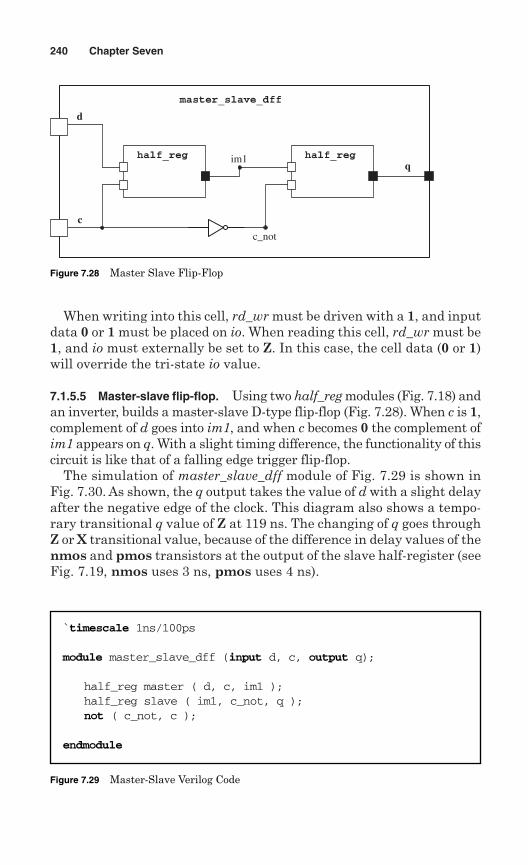
When writing into this cell, rd_wr must be driven with a 1, and inputdata 0 or 1 must be placed on io. When reading this cell, rd_wr must be1, and io must externally be set to Z. In this case, the cell data (0 or 1)will override the tri-state io value.
7.1.5.5 Master-slave flip-flop. Using two half_reg modules (Fig. 7.18) andan inverter, builds a master-slave D-type flip-flop (Fig. 7.28). When c is 1,complement of d goes into im1, and when c becomes 0 the complement ofim1 appears on q. With a slight timing difference, the functionality of thiscircuit is like that of a falling edge trigger flip-flop.
The simulation of master_slave_dff module of Fig. 7.29 is shown inFig. 7.30. As shown, the q output takes the value of d with a slight delayafter the negative edge of the clock. This diagram also shows a tempo-rary transitional q value of Z at 119 ns. The changing of q goes throughZ or X transitional value, because of the difference in delay values of thenmos and pmos transistors at the output of the slave half-register (seeFig. 7.19, nmos uses 3 ns, pmos uses 4 ns).
240 Chapter Seven
d
master_slave_dff
im1half_reg
c
q
c_not
half_reg
Figure 7.28 Master Slave Flip-Flop
Figure 7.29 Master-Slave Verilog Code
`timescale 1ns/100ps
module master_slave_dff (input d, c, output q);
half_reg master ( d, c, im1 );half_reg slave ( im1, c_not, q );not ( c_not, c );
endmodule
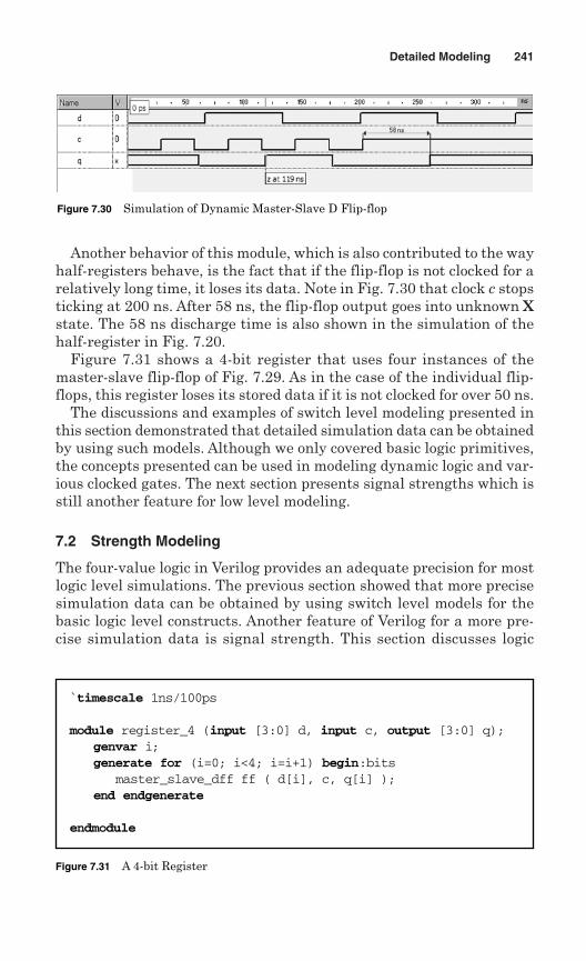
Another behavior of this module, which is also contributed to the wayhalf-registers behave, is the fact that if the flip-flop is not clocked for arelatively long time, it loses its data. Note in Fig. 7.30 that clock c stopsticking at 200 ns. After 58 ns, the flip-flop output goes into unknown Xstate. The 58 ns discharge time is also shown in the simulation of thehalf-register in Fig. 7.20.
Figure 7.31 shows a 4-bit register that uses four instances of themaster-slave flip-flop of Fig. 7.29. As in the case of the individual flip-flops, this register loses its stored data if it is not clocked for over 50 ns.
The discussions and examples of switch level modeling presented inthis section demonstrated that detailed simulation data can be obtainedby using such models. Although we only covered basic logic primitives,the concepts presented can be used in modeling dynamic logic and var-ious clocked gates. The next section presents signal strengths which isstill another feature for low level modeling.
7.2 Strength Modeling
The four-value logic in Verilog provides an adequate precision for mostlogic level simulations. The previous section showed that more precisesimulation data can be obtained by using switch level models for thebasic logic level constructs. Another feature of Verilog for a more pre-cise simulation data is signal strength. This section discusses logic
Detailed Modeling 241
Figure 7.30 Simulation of Dynamic Master-Slave D Flip-flop
Figure 7.31 A 4-bit Register
`timescale 1ns/100ps
module register_4 (input [3:0] d, input c, output [3:0] q);genvar i;generate for (i=0; i<4; i=i+1) begin:bits
master_slave_dff ff ( d[i], c, q[i] );end endgenerate
endmodule
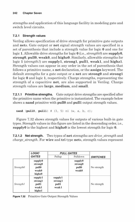
strengths and application of this language facility in modeling gate andswitch level circuits.
7.2.1 Strength values
Verilog allows specification of drive strength for primitive gate outputsand nets. Gate output or net signal strength values are specified in aset of parenthesis that include a strength value for logic 0 and one forlogic 1. Allowable drive strengths for logic 0 (i.e., strength0) are supply0,strong0, pull0, weak0, and highz0. Similarly, allowable strengths forlogic 1 (strength1) are supply1, strong1, pull1, weak1, and highz1.Strength values can appear in any order in the set of parenthesis thatfollows a primitive name, a net declaration, or the assign keyword. Thedefault strengths for a gate output or a net are strong0 and strong1for logic 0 and logic 1, respectively. Charge strengths, representing thestrength of a capacitive net, are also supported in Verilog. Chargestrength values are large, medium, and small.
7.2.1.1 Primitive strengths. Gate output drive strengths are specified afterthe primitive name when the primitive is instantiated. The example belowshows a nand primitive with pull0 and pull1 output strength values.
nand (pull0, pull1) # (3, 5) n1 (w, a, b, c);
Figure 7.32 shows strength values for outputs of various built-in gatetypes. Strength values in this figure are listed in the descending order, i.e.,supply0 is the highest and highz0 is the lowest strength for logic 0.
7.2.1.2 Net strength. Two types of net strengths are drive_strength andcharge_strength. For wire and tri type nets, strength values represent
242 Chapter Seven
PULL GATESLOGICGATES Pullup Pulldown SWITCHES
Strength0
supply0strong0
pull0weak0highz0
supply0strong0
pull0weak0
No strength
Strength1
supply1strong1
pull1weak1highz1
supply1strong1
pull1weak1
No strength
Figure 7.32 Primitive Gate Output Strength Values
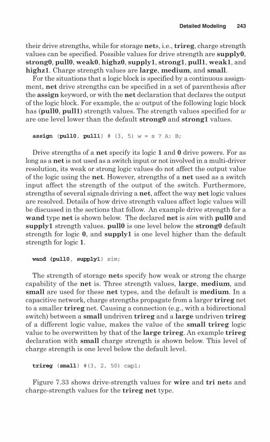
their drive strengths, while for storage nets, i.e., trireg, charge strengthvalues can be specified. Possible values for drive strength are supply0,strong0, pull0, weak0, highz0, supply1, strong1, pull1, weak1, andhighz1. Charge strength values are large, medium, and small.
For the situations that a logic block is specified by a continuous assign-ment, net drive strengths can be specified in a set of parenthesis afterthe assign keyword, or with the net declaration that declares the outputof the logic block. For example, the w output of the following logic blockhas (pull0, pull1) strength values. The strength values specified for ware one level lower than the default strong0 and strong1 values.
assign (pull0, pull1) # (3, 5) w = s ? A: B;
Drive strengths of a net specify its logic 1 and 0 drive powers. For aslong as a net is not used as a switch input or not involved in a multi-driverresolution, its weak or strong logic values do not affect the output valueof the logic using the net. However, strengths of a net used as a switchinput affect the strength of the output of the switch. Furthermore,strengths of several signals driving a net, affect the way net logic valuesare resolved. Details of how drive strength values affect logic values willbe discussed in the sections that follow. An example drive strength for awand type net is shown below. The declared net is sim with pull0 andsupply1 strength values. pull0 is one level below the strong0 defaultstrength for logic 0, and supply1 is one level higher than the defaultstrength for logic 1.
wand (pull0, supply1) sim;
The strength of storage nets specify how weak or strong the chargecapability of the net is. Three strength values, large, medium, andsmall are used for these net types, and the default is medium. In acapacitive network, charge strengths propagate from a larger trireg netto a smaller trireg net. Causing a connection (e.g., with a bidirectionalswitch) between a small undriven trireg and a large undriven triregof a different logic value, makes the value of the small trireg logicvalue to be overwritten by that of the large trireg. An example triregdeclaration with small charge strength is shown below. This level ofcharge strength is one level below the default level.
trireg (small) #(3, 2, 50) cap1;
Figure 7.33 shows drive-strength values for wire and tri nets andcharge-strength values for the trireg net type.
Detailed Modeling 243
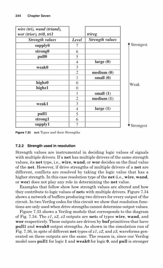
244 Chapter Seven
wire (tri), wand (triand),wor (trior), tri0, tri1 trireg
Strength values Level Strength valuessupply0 7strong0 6
pull0 54 large (0)
weak0 32 medium (0)1 small (0)
highz0 0highz1 0
1 small (1)2 medium (1)
weak1 34 large (1)
pull1 5strong1 6supply1 7
Strongest
Strongest
Weak
Figure 7.33 net Types and their Strengths
7.2.2 Strength used in resolution
Strength values are instrumental in deciding logic values of signalswith multiple drivers. If a net has multiple drivers of the same strengthvalues, its net type, i.e., wire, wand, or wor decides on the final valueof the net. However, if drive strengths of multiple drivers of a net aredifferent, conflicts are resolved by taking the logic value that has ahigher strength. In this case resolution type of the net (i.e., wire, wand,or wor) does not play any role in determining the net value.
Examples that follow show how strength values are altered and howthey contribute to logic values of nets with multiple drivers. Figure 7.34shows a network of buffers producing two drivers for every output of thecircuit. In two Verilog codes for this circuit we show that resolution func-tions are only used when drive strengths cannot determine output values.
Figure 7.35 shows a Verilog module that corresponds to the diagramof Fig. 7.34. The z1, z2, z3 outputs are nets of types wire, wand, andwor respectively. These outputs are driven by buf primitives that havepull1 and weak0 output strengths. As shown in the simulation run ofFig. 7.36, in spite of different net types of z1, z2, and z3, waveforms gen-erated on these outputs are the same. The reason is, since our Verilogmodel uses pull1 for logic 1 and weak0 for logic 0, and pull is stronger
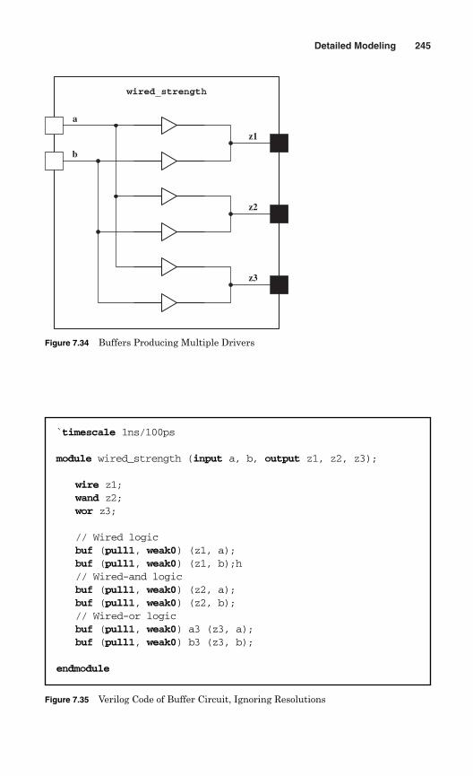
Detailed Modeling 245
a
wired_strength
b
z1
z2
z3
Figure 7.34 Buffers Producing Multiple Drivers
Figure 7.35 Verilog Code of Buffer Circuit, Ignoring Resolutions
`timescale 1ns/100ps
module wired_strength (input a, b, output z1, z2, z3);
wire z1;wand z2;wor z3;
// Wired logicbuf (pull1, weak0) (z1, a);buf (pull1, weak0) (z1, b);h// Wired-and logicbuf (pull1, weak0) (z2, a);buf (pull1, weak0) (z2, b);// Wired-or logicbuf (pull1, weak0) a3 (z3, a);buf (pull1, weak0) b3 (z3, b);
endmodule
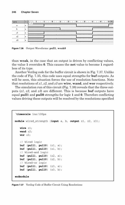
246 Chapter Seven
Figure 7.36 Output Waveforms: pull1, weak0
Figure 7.37 Verilog Code of Buffer Circuit Using Resolutions
`timescale 1ns/100ps
module wired_strength (input a, b, output z1, z2, z3);
wire z1;wand z2;wor z3;
// Wired logicbuf (pull1, pull0) (z1, a);buf (pull1, pull0) (z1, b);// Wired-and logicbuf (pull1, pull0) (z2, a);buf (pull1, pull0) (z2, b);// Wired-or logicbuf (pull1, pull0) (z3, a);buf (pull1, pull0) (z3, b);
endmodule
than weak, in the case that an output is driven by conflicting values,the value 1 overrides 0. This causes the net value to become 1 regard-less of its type.
Another Verilog code for the buffer circuit is shown in Fig. 7.37. Unlikethe code of Fig. 7.35, this code uses equal strengths for buf outputs. Aswill be seen, this situation forces the use of resolution functions. Notethat resolutions of z1, z2, and z3 are wire, wand, and wor respectively.
The simulation run of this circuit (Fig. 7.38) reveals that the three out-puts (z1, z2, and z3) are different. This is because buf outputs haveequal pull1 and pull0 strengths for logic 1 and 0. Therefore conflictingvalues driving these outputs will be resolved by the resolutions specified
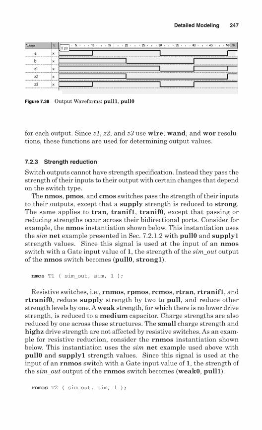
for each output. Since z1, z2, and z3 use wire, wand, and wor resolu-tions, these functions are used for determining output values.
7.2.3 Strength reduction
Switch outputs cannot have strength specification. Instead they pass thestrength of their inputs to their output with certain changes that dependon the switch type.
The nmos, pmos, and cmos switches pass the strength of their inputsto their outputs, except that a supply strength is reduced to strong.The same applies to tran, tranif1, tranif0, except that passing orreducing strengths occur across their bidirectional ports. Consider forexample, the nmos instantiation shown below. This instantiation usesthe sim net example presented in Sec. 7.2.1.2 with pull0 and supply1strength values. Since this signal is used at the input of an nmosswitch with a Gate input value of 1, the strength of the sim_out outputof the nmos switch becomes (pull0, strong1).
nmos T1 ( sim_out, sim, 1 );
Resistive switches, i.e., rnmos, rpmos, rcmos, rtran, rtranif1, andrtranif0, reduce supply strength by two to pull, and reduce otherstrength levels by one. A weak strength, for which there is no lower drivestrength, is reduced to a medium capacitor. Charge strengths are alsoreduced by one across these structures. The small charge strength andhighz drive strength are not affected by resistive switches. As an exam-ple for resistive reduction, consider the rnmos instantiation shownbelow. This instantiation uses the sim net example used above withpull0 and supply1 strength values. Since this signal is used at theinput of an rnmos switch with a Gate input value of 1, the strength ofthe sim_out output of the rnmos switch becomes (weak0, pull1).
rnmos T2 ( sim_out, sim, 1 );
Detailed Modeling 247
Figure 7.38 Output Waveforms: pull1, pull0
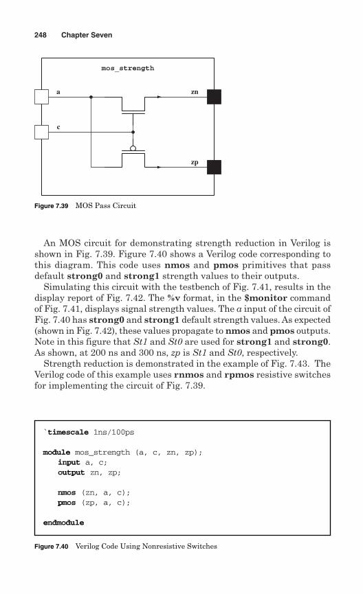
An MOS circuit for demonstrating strength reduction in Verilog isshown in Fig. 7.39. Figure 7.40 shows a Verilog code corresponding tothis diagram. This code uses nmos and pmos primitives that passdefault strong0 and strong1 strength values to their outputs.
Simulating this circuit with the testbench of Fig. 7.41, results in thedisplay report of Fig. 7.42. The %v format, in the $monitor commandof Fig. 7.41, displays signal strength values. The a input of the circuit ofFig. 7.40 has strong0 and strong1 default strength values. As expected(shown in Fig. 7.42), these values propagate to nmos and pmos outputs.Note in this figure that St1 and St0 are used for strong1 and strong0.As shown, at 200 ns and 300 ns, zp is St1 and St0, respectively.
Strength reduction is demonstrated in the example of Fig. 7.43. TheVerilog code of this example uses rnmos and rpmos resistive switchesfor implementing the circuit of Fig. 7.39.
248 Chapter Seven
a
mos_strength
c
zn
zp
Figure 7.39 MOS Pass Circuit
Figure 7.40 Verilog Code Using Nonresistive Switches
`timescale 1ns/100ps
module mos_strength (a, c, zn, zp);input a, c;output zn, zp;
nmos (zn, a, c);pmos (zp, a, c);
endmodule
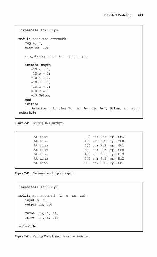
Detailed Modeling 249
Figure 7.41 Testing mos_strength
`timescale 1ns/100ps
module test_mos_strength;reg a, c;wire zn, zp;
mos_strength cut (a, c, zn, zp);
initial begin#10 a = 1;#10 c = 0;#10 a = 0;#10 c = 1;#10 a = 1;#10 c = 0;#10 $stop;
endinitial
$monitor (“At time %t zn: %v, zp: %v”, $time, zn, zp);endmodule
Figure 7.42 Nonresistive Display Report
At time 0 zn: StX, zp: StXAt time 100 zn: StH, zp: StHAt time 200 zn: HiZ, zp: St1At time 300 zn: HiZ, zp: St0At time 400 zn: St0, zp: HiZAt time 500 zn: St1, zp: HiZAt time 600 zn: HiZ, zp: St1
Figure 7.43 Verilog Code Using Resistive Switches
`timescale 1ns/100ps
module mos_strength (a, c, zn, zp);input a, c;output zn, zp;
rnmos (zn, a, c); rpmos (zp, a, c);
endmodule
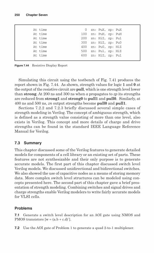
Simulating this circuit using the testbench of Fig. 7.41 produces thereport shown in Fig. 7.44. As shown, strength values for logic 1 and 0 atthe output of the resistive circuit are pull, which is one strength level lowerthan strong. At 200 ns and 300 ns when a propagates to zp its strengthsare reduced from strong1 and strong0 to pull1 and pull0. Similarly, at400 ns and 500 ns, zn output strengths become pull0 and pull1.
Sections 7.2.2 and 7.2.3 briefly discussed several simple cases ofstrength modeling in Verilog. The concept of ambiguous strength, whichis defined as a strength value consisting of more than one level, alsoexists in Verilog. This concept and more details of charge and drivestrengths can be found in the standard IEEE Language ReferenceManual for Verilog.
7.3 Summary
This chapter discussed some of the Verilog features to generate detailedmodels for components of a cell library or an existing set of parts. Thesefeatures are not synthesizable and their only purpose is to generateaccurate models. The first part of this chapter discussed switch levelVerilog models. We discussed unidirectional and bidirectional switches.We also showed the use of capacitive nodes as a means of storing memorydata. More complex switch level structures can be modeled using con-cepts presented here. The second part of this chapter gave a brief pres-entation of strength modeling. Combining switches and signal drives andcharge strengths enable Verilog modelers to write fairly accurate modelsfor VLSI cells.
Problems
7.1 Generate a switch level description for an AOI gate using NMOS andPMOS transistors [w = (a.b + c.d)`].
7.2 Use the AOI gate of Problem 1 to generate a quad 2-to-1 multiplexer.
250 Chapter Seven
Figure 7.44 Resistive Display Report
At time 0 zn: PuX, zp: PuXAt time 100 zn: PuH, zp: PuHAt time 200 zn: HiZ, zp: Pu1At time 300 zn: HiZ, zp: Pu0At time 400 zn: Pu0, zp: HiZAt time 500 zn: Pu1, zp: HiZAt time 600 zn: HiZ, zp: Pu1
7.3 Generate a switch level description for a MAJ (Majority) gate using NMOSand PMOS transistors (w = a.b + a.c + b.c ).
7.4 After minimization of the following function, show its transistor levelCMOS implementation. Use a single complex gate for realizing this function.Available to you are all inputs and their complements. Your implementationshould use a minimum number of transistors.
f (a, b, c, d) = a’ . c’ . d’ + b . d’
Suggested Reading
Brown, S., and Z. Vranesic, Fundamentals of Digital Logic with Verilog Design, McGraw-Hill, New York, 2002, ISBN: 0-07-283878-7.
IEEE Std 1364-2001, IEEE Standard Verilog Language Reference Manual, SH94921-TBR (print) SS94921-TBR (electronic), ISBN 0-7381-2827-9 (print and electronic),2001.
Uyemura, J.P. Introduction to VLSI Circuits and Systems, John Wiley & Sons, Hoboken,New Jersey, USA, 2002, ISBN: 0471127043.
Weste, N.H.E, and D. Harris, CMOS VLSI Design: A Circuits and Systems Perspective(3rd Edition), 3rd ed, Addison Wesley, Boston, MA, 2004, ISBN: 0321149017.
Detailed Modeling 251

This page intentionally left blank
Chapter
8RT Level Design and Test
This chapter discusses design and test of complete systems. Topics dis-cussed in Chaps. 4, 5, and 6 are used here to describe systems for syn-thesis and develop testbenches for these complete systems. We willshow how a design is partitioned into its datapath and controller andhow these components are described in Verilog. In a complex design wewill show further partitioning of the datapath of the design into its indi-vidual registers, busses, and logic units. For testing our designs, weshow how interactive testing and use of files are utilized for testingactual systems. The chapter begins with specification and design of asequential multiplier. We will then discuss a simple processor to famil-iarize readers with design methodology that we are promoting for largersystems. The last section of this chapter uses our design methodologyto design, code and test a CPU with a typical architecture.
8.1 Sequential Multiplier
Our first example of RT level system design is an add-and-shift sequen-tial multiplier, with 8-bit A and B inputs and a 16-bit result. The blockdiagram of this circuit is shown in Fig. 8.1. This multiplier has an 8-bitbidirectional I/O for inputting its A and B operands, and outputting its16-bit output one byte at a time.
Multiplication begins with the start pulse. On the clock edge thatstart is 1, operand A is on the databus and in the next clock, this buswill contain operand B. The two operands appear on the bus in two con-secutive clock pulses. After accepting these data inputs, the multiplierbegins its multiplication process and when it is completed, it starts send-ing the result out on the databus. When the least-significant byte is placedon databus, the lsb_out output is issued, and for the most-significant byte,
253
Copyright © 2006 by The McGraw-Hill Publishing Companies, Inc. Click here for terms of use.
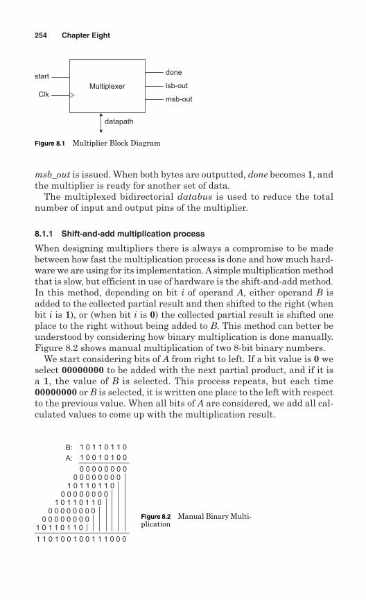
msb_out is issued. When both bytes are outputted, done becomes 1, andthe multiplier is ready for another set of data.
The multiplexed bidirectorial databus is used to reduce the totalnumber of input and output pins of the multiplier.
8.1.1 Shift-and-add multiplication process
When designing multipliers there is always a compromise to be madebetween how fast the multiplication process is done and how much hard-ware we are using for its implementation. A simple multiplication methodthat is slow, but efficient in use of hardware is the shift-and-add method.In this method, depending on bit i of operand A, either operand B isadded to the collected partial result and then shifted to the right (whenbit i is 1), or (when bit i is 0) the collected partial result is shifted oneplace to the right without being added to B. This method can better beunderstood by considering how binary multiplication is done manually.Figure 8.2 shows manual multiplication of two 8-bit binary numbers.
We start considering bits of A from right to left. If a bit value is 0 weselect 00000000 to be added with the next partial product, and if it isa 1, the value of B is selected. This process repeats, but each time00000000 or B is selected, it is written one place to the left with respectto the previous value. When all bits of A are considered, we add all cal-culated values to come up with the multiplication result.
254 Chapter Eight
start
Clklsb-out
done
msb-out
datapath
Multiplexer
Figure 8.1 Multiplier Block Diagram
1 0 1 1 0 1 1 0
1 0 0 1 0 1 0 0
0 0 0 0 0 0 0 00 0 0 0 0 0 0 0
1 0 1 1 0 1 1 00 0 0 0 0 0 0 0
1 0 1 1 0 1 1 00 0 0 0 0 0 0 0
0 0 0 0 0 0 0 01 0 1 1 0 1 1 0
1 1 0 1 0 0 1 0 0 1 1 1 0 0 0
B:
A:
Figure 8.2 Manual Binary Multi-plication
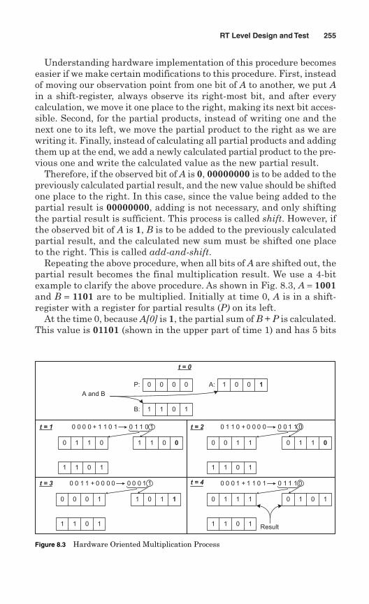
Understanding hardware implementation of this procedure becomeseasier if we make certain modifications to this procedure. First, insteadof moving our observation point from one bit of A to another, we put Ain a shift-register, always observe its right-most bit, and after everycalculation, we move it one place to the right, making its next bit acces-sible. Second, for the partial products, instead of writing one and thenext one to its left, we move the partial product to the right as we arewriting it. Finally, instead of calculating all partial products and addingthem up at the end, we add a newly calculated partial product to the pre-vious one and write the calculated value as the new partial result.
Therefore, if the observed bit of A is 0, 00000000 is to be added to thepreviously calculated partial result, and the new value should be shiftedone place to the right. In this case, since the value being added to thepartial result is 00000000, adding is not necessary, and only shiftingthe partial result is sufficient. This process is called shift. However, ifthe observed bit of A is 1, B is to be added to the previously calculatedpartial result, and the calculated new sum must be shifted one placeto the right. This is called add-and-shift.
Repeating the above procedure, when all bits of A are shifted out, thepartial result becomes the final multiplication result. We use a 4-bitexample to clarify the above procedure. As shown in Fig. 8.3, A = 1001and B = 1101 are to be multiplied. Initially at time 0, A is in a shift-register with a register for partial results (P) on its left.
At the time 0, because A[0] is 1, the partial sum of B + P is calculated.This value is 01101 (shown in the upper part of time 1) and has 5 bits
RT Level Design and Test 255
0 0 00P: 0 0 11A:
1 0 11B:
t = 0
1 1 00 1 0 01
1 0 11
t = 1 0 0 0 0 + 1 1 0 1 0 1 1 0 1
0 1 10 1 1 00
1 0 11
t = 2 0 1 1 0 + 0 0 0 0 0 0 1 1 0
0 0 10 0 1 11
1 0 11
t = 3 0 0 1 1 + 0 0 0 0 0 0 0 1 1
1 1 10 1 0 10
1 0 11
t = 4 0 0 0 1 + 1 1 0 1 0 1 1 1 0
A and B
Result
Figure 8.3 Hardware Oriented Multiplication Process
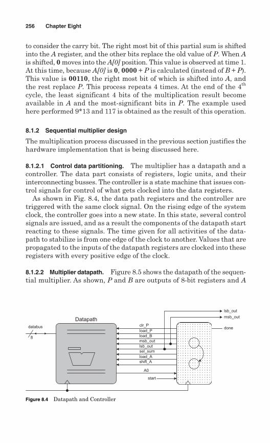
to consider the carry bit. The right most bit of this partial sum is shiftedinto the A register, and the other bits replace the old value of P. When Ais shifted, 0 moves into the A[0] position. This value is observed at time 1.At this time, because A[0] is 0, 0000 + P is calculated (instead of B + P).This value is 00110, the right most bit of which is shifted into A, andthe rest replace P. This process repeats 4 times. At the end of the 4th
cycle, the least significant 4 bits of the multiplication result becomeavailable in A and the most-significant bits in P. The example usedhere performed 9*13 and 117 is obtained as the result of this operation.
8.1.2 Sequential multiplier design
The multiplication process discussed in the previous section justifies thehardware implementation that is being discussed here.
8.1.2.1 Control data partitioning. The multiplier has a datapath and acontroller. The data part consists of registers, logic units, and theirinterconnecting busses. The controller is a state machine that issues con-trol signals for control of what gets clocked into the data registers.
As shown in Fig. 8.4, the data path registers and the controller aretriggered with the same clock signal. On the rising edge of the systemclock, the controller goes into a new state. In this state, several controlsignals are issued, and as a result the components of the datapath startreacting to these signals. The time given for all activities of the data-path to stabilize is from one edge of the clock to another. Values that arepropagated to the inputs of the datapath registers are clocked into theseregisters with every positive edge of the clock.
8.1.2.2 Multiplier datapath. Figure 8.5 shows the datapath of the sequen-tial multiplier. As shown, P and B are outputs of 8-bit registers and A
256 Chapter Eight
Datapath
databus
8
clr_P
load_P
load_B
msb_out
lsb_outsel_sum
load_Ashift_A
start
lsb_out
msb_out
done
A0
Figure 8.4 Datapath and Controller
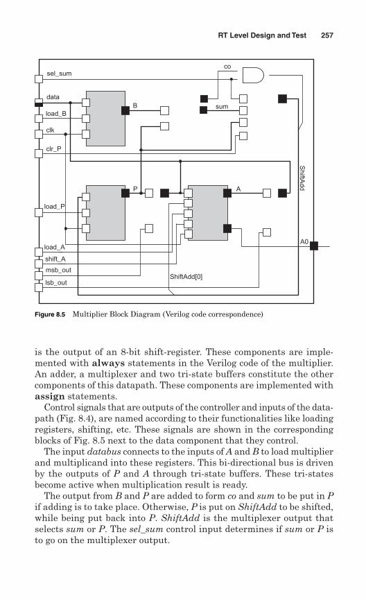
is the output of an 8-bit shift-register. These components are imple-mented with always statements in the Verilog code of the multiplier.An adder, a multiplexer and two tri-state buffers constitute the othercomponents of this datapath. These components are implemented withassign statements.
Control signals that are outputs of the controller and inputs of the data-path (Fig. 8.4), are named according to their functionalities like loadingregisters, shifting, etc. These signals are shown in the correspondingblocks of Fig. 8.5 next to the data component that they control.
The input databus connects to the inputs of A and B to load multiplierand multiplicand into these registers. This bi-directional bus is drivenby the outputs of P and A through tri-state buffers. These tri-statesbecome active when multiplication result is ready.
The output from B and P are added to form co and sum to be put in Pif adding is to take place. Otherwise, P is put on ShiftAdd to be shifted,while being put back into P. ShiftAdd is the multiplexer output thatselects sum or P. The sel_sum control input determines if sum or P isto go on the multiplexer output.
RT Level Design and Test 257
sel_sumco
sumBdata
load_B
clk
clr_P
load_P
A0
AP
load_A
msb_out
lsb_out
shift_A
ShiftAdd[0]
ShiftA
dd
Figure 8.5 Multiplier Block Diagram (Verilog code correspondence)
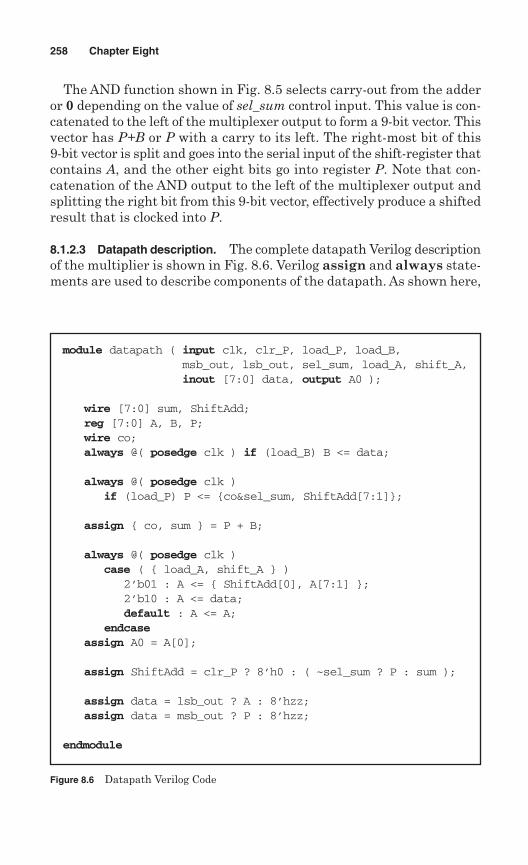
The AND function shown in Fig. 8.5 selects carry-out from the adderor 0 depending on the value of sel_sum control input. This value is con-catenated to the left of the multiplexer output to form a 9-bit vector. Thisvector has P+B or P with a carry to its left. The right-most bit of this9-bit vector is split and goes into the serial input of the shift-register thatcontains A, and the other eight bits go into register P. Note that con-catenation of the AND output to the left of the multiplexer output andsplitting the right bit from this 9-bit vector, effectively produce a shiftedresult that is clocked into P.
8.1.2.3 Datapath description. The complete datapath Verilog descriptionof the multiplier is shown in Fig. 8.6. Verilog assign and always state-ments are used to describe components of the datapath. As shown here,
258 Chapter Eight
Figure 8.6 Datapath Verilog Code
module datapath ( input clk, clr_P, load_P, load_B, msb_out, lsb_out, sel_sum, load_A, shift_A,inout [7:0] data, output A0 );
wire [7:0] sum, ShiftAdd;reg [7:0] A, B, P;wire co;always @( posedge clk ) if (load_B) B <= data;
always @( posedge clk ) if (load_P) P <= {co&sel_sum, ShiftAdd[7:1]};
assign { co, sum } = P + B;
always @( posedge clk )case ( { load_A, shift_A } )
2’b01 : A <= { ShiftAdd[0], A[7:1] };2’b10 : A <= data;default : A <= A;
endcaseassign A0 = A[0];
assign ShiftAdd = clr_P ? 8’h0 : ( ~sel_sum ? P : sum );
assign data = lsb_out ? A : 8’hzz;assign data = msb_out ? P : 8’hzz;
endmodule
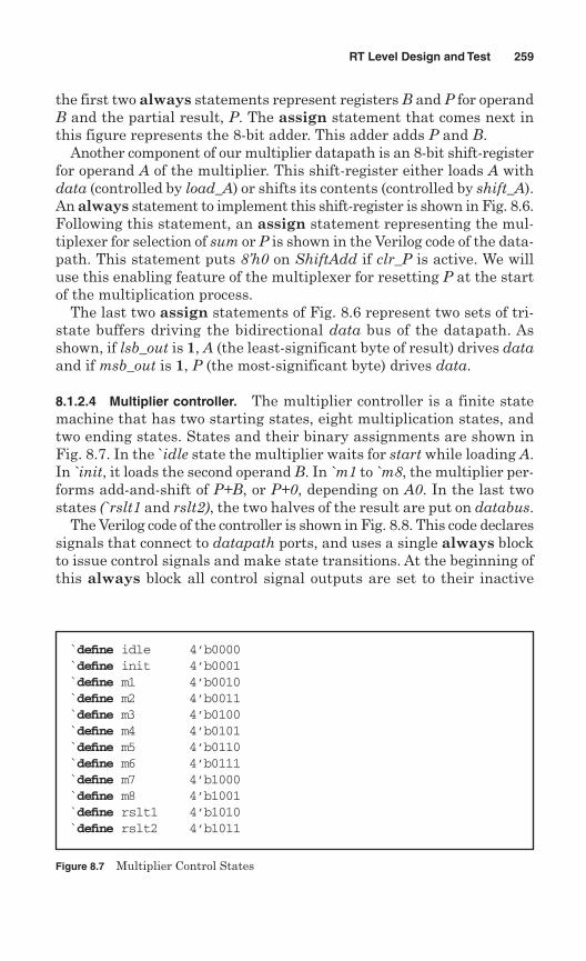
the first two always statements represent registers B and P for operandB and the partial result, P. The assign statement that comes next inthis figure represents the 8-bit adder. This adder adds P and B.
Another component of our multiplier datapath is an 8-bit shift-registerfor operand A of the multiplier. This shift-register either loads A withdata (controlled by load_A) or shifts its contents (controlled by shift_A).An always statement to implement this shift-register is shown in Fig. 8.6.Following this statement, an assign statement representing the mul-tiplexer for selection of sum or P is shown in the Verilog code of the data-path. This statement puts 8’h0 on ShiftAdd if clr_P is active. We willuse this enabling feature of the multiplexer for resetting P at the startof the multiplication process.
The last two assign statements of Fig. 8.6 represent two sets of tri-state buffers driving the bidirectional data bus of the datapath. Asshown, if lsb_out is 1, A (the least-significant byte of result) drives dataand if msb_out is 1, P (the most-significant byte) drives data.
8.1.2.4 Multiplier controller. The multiplier controller is a finite statemachine that has two starting states, eight multiplication states, andtwo ending states. States and their binary assignments are shown inFig. 8.7. In the ̀ idle state the multiplier waits for start while loading A.In ̀ init, it loads the second operand B. In ̀ m1 to ̀ m8, the multiplier per-forms add-and-shift of P+B, or P+0, depending on A0. In the last twostates (`rslt1 and rslt2), the two halves of the result are put on databus.
The Verilog code of the controller is shown in Fig. 8.8. This code declaressignals that connect to datapath ports, and uses a single always blockto issue control signals and make state transitions. At the beginning ofthis always block all control signal outputs are set to their inactive
RT Level Design and Test 259
Figure 8.7 Multiplier Control States
`define idle 4’b0000`define init 4’b0001`define m1 4’b0010`define m2 4’b0011`define m3 4’b0100`define m4 4’b0101`define m5 4’b0110`define m6 4’b0111`define m7 4’b1000`define m8 4’b1001`define rslt1 4’b1010`define rslt2 4’b1011
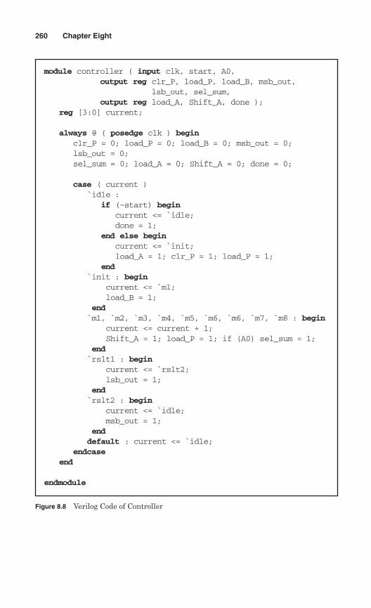
260 Chapter Eight
Figure 8.8 Verilog Code of Controller
module controller ( input clk, start, A0, output reg clr_P, load_P, load_B, msb_out,
lsb_out, sel_sum, output reg load_A, Shift_A, done );
reg [3:0] current;
always @ ( posedge clk ) beginclr_P = 0; load_P = 0; load_B = 0; msb_out = 0;lsb_out = 0;sel_sum = 0; load_A = 0; Shift_A = 0; done = 0;
case ( current )`idle :
if (~start) begincurrent <= `idle;done = 1;
end else begincurrent <= `init; load_A = 1; clr_P = 1; load_P = 1;
end`init : begin
current <= `m1; load_B = 1;
end`m1, `m2, `m3, `m4, `m5, `m6, `m6, `m7, `m8 : begin
current <= current + 1; Shift_A = 1; load_P = 1; if (A0) sel_sum = 1;
end`rslt1 : begin
current <= `rslt2; lsb_out = 1;
end`rslt2 : begin
current <= `idle; msb_out = 1;
enddefault : current <= `idle;
endcaseend
endmodule
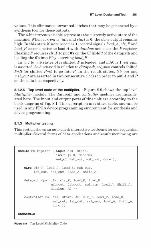
values. This eliminates unwanted latches that may be generated by asynthesis tool for these outputs.
The 4-bit current variable represents the currently active state of themachine. When current is `idle and start is 0, the done output remainshigh. In this state if start becomes 1, control signals load_A, clr_P andload_P become active to load A with databus and clear the P register.Clearing P requires clr_P to put 0’s on the ShiftAdd of the datapath andloading the 0’s into P by asserting load_P.
In `m1 to `m8 states, A is shifted, P is loaded, and if A0 is 1, sel_sumis asserted. As discussed in relation to datapath, sel_sum controls shiftedP+B (or shifted P+0) to go into P. In the result states, lsb_out andmsb_out are asserted in two consecutive clocks in order to put A and Pon the data bus respectively.
8.1.2.5 Top-level code of the multiplier. Figure 8.9 shows the top-levelMultiplier module. The datapath and controller modules are instanti-ated here. The input and output ports of this unit are according to theblock diagram of Fig. 8.1. This description is synthesizable, and can beused in any FPGA device programming environment for synthesis anddevice programming.
8.1.3 Multiplier testing
This section shows an auto-check interactive testbench for our sequentialmultiplier. Several forms of data applications and result monitoring are
RT Level Design and Test 261
Figure 8.9 Top-Level Multiplier Code
module Multiplier ( input clk, start,inout [7:0] databus, output lsb_out, msb_out, done );
wire clr_P, load_P, load_B, msb_out, lsb_out, sel_sum, load_A, Shift_A;
datapath dpu( clk, clr_P, load_P, load_B,msb_out, lsb_out, sel_sum, load_A, Shift_A, databus, A0 );
controller cu( clk, start, A0, clr_P, load_P, load_B,msb_out, lsb_out, sel_sum, load_A, Shift_A,done );
endmodule
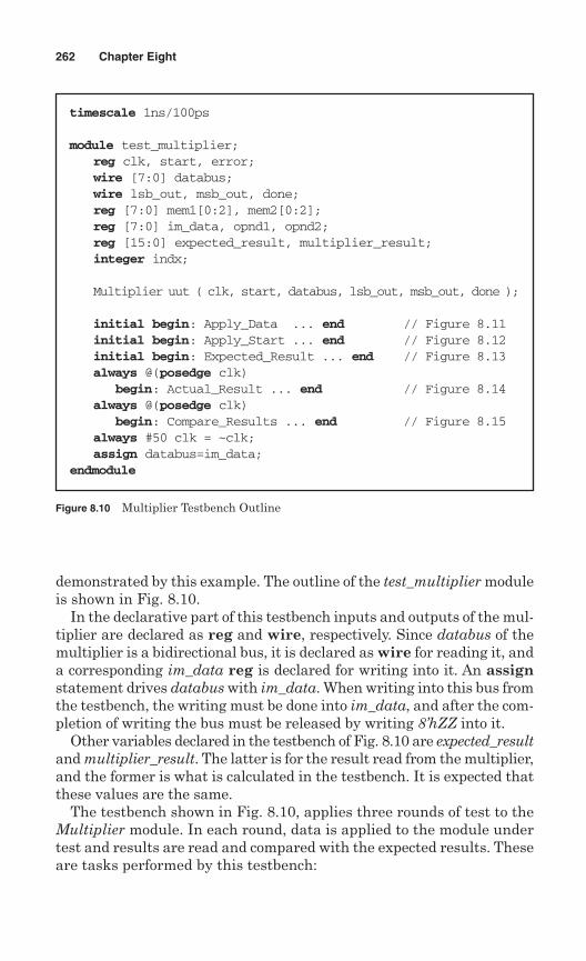
demonstrated by this example. The outline of the test_multiplier moduleis shown in Fig. 8.10.
In the declarative part of this testbench inputs and outputs of the mul-tiplier are declared as reg and wire, respectively. Since databus of themultiplier is a bidirectional bus, it is declared as wire for reading it, anda corresponding im_data reg is declared for writing into it. An assignstatement drives databus with im_data. When writing into this bus fromthe testbench, the writing must be done into im_data, and after the com-pletion of writing the bus must be released by writing 8’hZZ into it.
Other variables declared in the testbench of Fig. 8.10 are expected_resultand multiplier_result. The latter is for the result read from the multiplier,and the former is what is calculated in the testbench. It is expected thatthese values are the same.
The testbench shown in Fig. 8.10, applies three rounds of test to theMultiplier module. In each round, data is applied to the module undertest and results are read and compared with the expected results. Theseare tasks performed by this testbench:
262 Chapter Eight
Figure 8.10 Multiplier Testbench Outline
timescale 1ns/100ps
module test_multiplier;reg clk, start, error;wire [7:0] databus;wire lsb_out, msb_out, done;reg [7:0] mem1[0:2], mem2[0:2];reg [7:0] im_data, opnd1, opnd2; reg [15:0] expected_result, multiplier_result;integer indx;
Multiplier uut ( clk, start, databus, lsb_out, msb_out, done );
initial begin: Apply_Data ... end // Figure 8.11initial begin: Apply_Start ... end // Figure 8.12initial begin: Expected_Result ... end // Figure 8.13always @(posedge clk)
begin: Actual_Result ... end // Figure 8.14always @(posedge clk)
begin: Compare_Results ... end // Figure 8.15always #50 clk = ~clk;assign databus=im_data;
endmodule
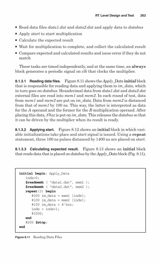
� Read data files data1.dat and data2.dat and apply data to databus� Apply start to start multiplication� Calculate the expected result� Wait for multiplication to complete, and collect the calculated result� Compare expected and calculated results and issue error if they do not
match
These tasks are timed independently, and at the same time, an alwaysblock generates a periodic signal on clk that clocks the multiplier.
8.1.3.1 Reading data files. Figure 8.11 shows the Apply_Data initial blockthat is responsible for reading data and applying them to im_data, whichin turn goes on databus. Hexadecimal data from data1.dat and data2.datexternal files are read into mem1 and mem2. In each round of test, datafrom mem1 and mem2 are put on im_data. Data from mem2 is distancedfrom that of mem1 by 100 ns. This way, the latter is interpreted as datafor the A operand and the former for the B multiplication operand. Afterplacing this data, 8’hzz is put on im_data. This releases the databus so thatit can be driven by the multiplier when its result is ready.
8.1.3.2 Applying start. Figure 8.12 shows an initial block in which vari-able initializations take place and start signal is issued. Using a repeatstatement, three 100 ns pulses distanced by 1400 ns are placed on start.
8.1.3.3 Calculating expected result. Figure 8.13 shows an initial blockthat reads data that is placed on databus by the Apply_Data block (Fig. 8.11),
RT Level Design and Test 263
Figure 8.11 Reading Data Files
initial begin: Apply_Dataindx=0;$readmemh ( “data1.dat”, mem1 );$readmemh ( “data2.dat”, mem2 );repeat(3) begin
#300 im_data = mem1 [indx]; #100 im_data = mem2 [indx]; #100 im_data = 8’hzz; indx = indx+1;#1000;
end#200 $stop;
end
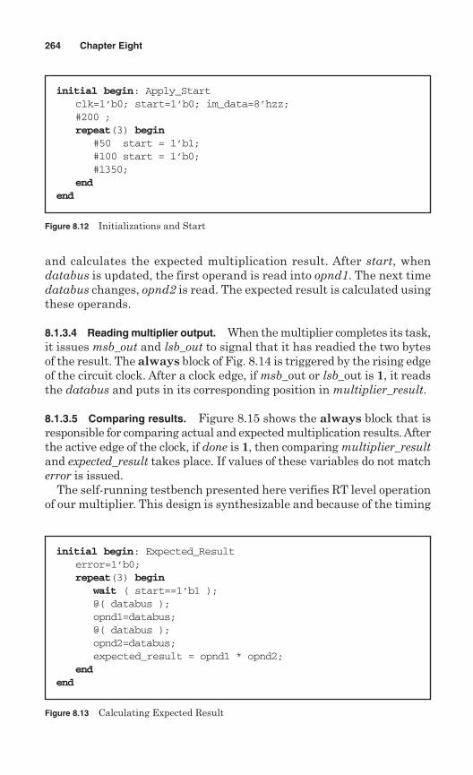
and calculates the expected multiplication result. After start, whendatabus is updated, the first operand is read into opnd1. The next timedatabus changes, opnd2 is read. The expected result is calculated usingthese operands.
8.1.3.4 Reading multiplier output. When the multiplier completes its task,it issues msb_out and lsb_out to signal that it has readied the two bytesof the result. The always block of Fig. 8.14 is triggered by the rising edgeof the circuit clock. After a clock edge, if msb_out or lsb_out is 1, it readsthe databus and puts in its corresponding position in multiplier_result.
8.1.3.5 Comparing results. Figure 8.15 shows the always block that isresponsible for comparing actual and expected multiplication results. Afterthe active edge of the clock, if done is 1, then comparing multiplier_resultand expected_result takes place. If values of these variables do not matcherror is issued.
The self-running testbench presented here verifies RT level operationof our multiplier. This design is synthesizable and because of the timing
264 Chapter Eight
Figure 8.12 Initializations and Start
initial begin: Apply_Startclk=1’b0; start=1’b0; im_data=8’hzz;#200 ;repeat(3) begin
#50 start = 1’b1;#100 start = 1’b0;#1350;
endend
Figure 8.13 Calculating Expected Result
initial begin: Expected_Resulterror=1’b0;repeat(3) begin
wait ( start==1’b1 );@( databus );opnd1=databus;@( databus );opnd2=databus;expected_result = opnd1 * opnd2;
endend
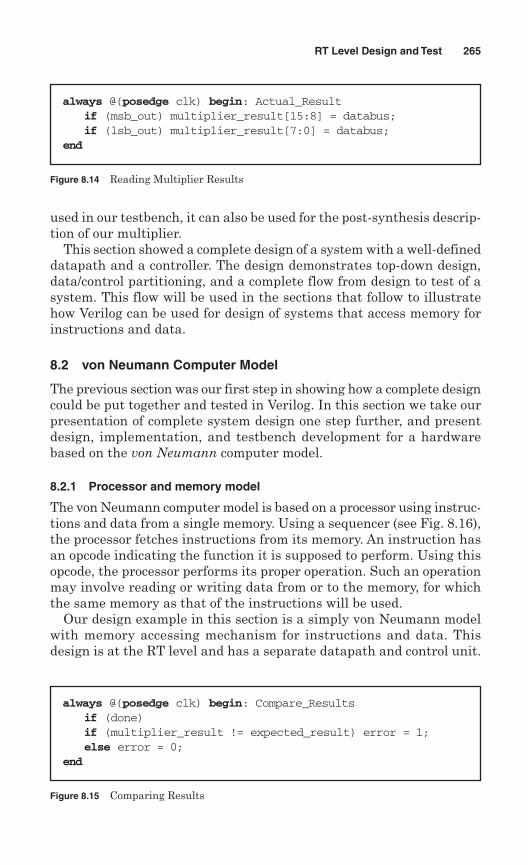
used in our testbench, it can also be used for the post-synthesis descrip-tion of our multiplier.
This section showed a complete design of a system with a well-defineddatapath and a controller. The design demonstrates top-down design,data/control partitioning, and a complete flow from design to test of asystem. This flow will be used in the sections that follow to illustratehow Verilog can be used for design of systems that access memory forinstructions and data.
8.2 von Neumann Computer Model
The previous section was our first step in showing how a complete designcould be put together and tested in Verilog. In this section we take ourpresentation of complete system design one step further, and presentdesign, implementation, and testbench development for a hardwarebased on the von Neumann computer model.
8.2.1 Processor and memory model
The von Neumann computer model is based on a processor using instruc-tions and data from a single memory. Using a sequencer (see Fig. 8.16),the processor fetches instructions from its memory. An instruction hasan opcode indicating the function it is supposed to perform. Using thisopcode, the processor performs its proper operation. Such an operationmay involve reading or writing data from or to the memory, for whichthe same memory as that of the instructions will be used.
Our design example in this section is a simply von Neumann modelwith memory accessing mechanism for instructions and data. Thisdesign is at the RT level and has a separate datapath and control unit.
RT Level Design and Test 265
Figure 8.14 Reading Multiplier Results
always @(posedge clk) begin: Actual_Resultif (msb_out) multiplier_result[15:8] = databus;if (lsb_out) multiplier_result[7:0] = databus;
end
Figure 8.15 Comparing Results
always @(posedge clk) begin: Compare_Resultsif (done)if (multiplier_result != expected_result) error = 1;else error = 0;
end
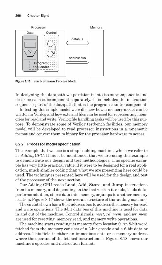
In designing the datapath we partition it into its subcomponents anddescribe each subcomponent separately. This includes the instructionsequencer part of the datapath that is the program counter component.
In testing this simple model we will show how a memory model can bewritten in Verilog and how external files can be used for representing mem-ories for read and write. Verilog file handling tasks will be used for this pur-pose. To demonstrate some of Verilog testbench facilities, our memorymodel will be developed to read processor instructions in a mnemonicformat and convert them to binary for the processor hardware to access.
8.2.2 Processor model specification
The example that we use is a simple adding machine, which we refer toas AddingCPU. It must be mentioned, that we are using this exampleto demonstrate our design and test methodologies. This specific exam-ple has very little practical value, if it were to be designed for a real appli-cation, much simpler coding than what we are presenting here could beused. The techniques presented here will be used for the design and testof the processor of the next section.
Our Adding CPU reads Load, Add, Store, and Jump instructionsfrom its memory, and depending on the instruction it reads, loads data,performs addition, stores data into memory, or jumps to another memorylocation. Figure 8.17 shows the overall structure of this adding machine.
The circuit shown has a 6-bit address bus to address the memory for readand write operations. The 8-bit data bus of this machine is used for datain and out of the machine. Control signals, reset, rd_mem, and wr_memare used for resetting, memory read, and memory write operations.
The machine starts reading its memory from location 0. An 8-bit wordfetched from the memory consists of a 2-bit opcode and a 6-bit data oraddress. This field is either an immediate data or a memory addresswhere the operand of the fetched instruction is. Figure 8.18 shows ourmachine’s opcodes and instruction format.
266 Chapter Eight
addressbus
databus
Program
sequencer
Processor
ControlData
Memory
Figure 8.16 von Neumann Process Model

The Adding CPU has a main register called AC (accumulator). TheLoad instruction directs the machine to load the addressed data fromthe memory into AC. The Store instruction causes contents of AC to bewritten into the addressed location in the memory. The operand of theAdd instruction is immd (immediate). This instruction adds immd tothe present contents of AC and puts the result back into AC. The Jumpinstruction loads the 6-bit address into the program counter of ourmachine, causing the next instruction to be fetched from this address.
8.2.3 Designing the adding CPU
The first step in the design of our adding machine is to decide on its dataand control partitioning and decide what goes into its data part and whatbehavior is expected from its controller.
The datapath of the design has the AC register for keeping data tooperate on, the PC register to keep track of the address being fetched,and an adder unit to perform the addition. In addition, the datapath has
RT Level Design and Test 267
Adding CPU
8 6adr_bus
rd_mem
wr_mem
data_bus
reset
clk
Figure 8.17 Interface of the Adding CPU Example
00
01
10
11
addr
addr
addr
immd
Load AC with (addr)
Store AC into (addr)
Jump to addr
Add Ac with immd
Figure 8.18 Instruction Format
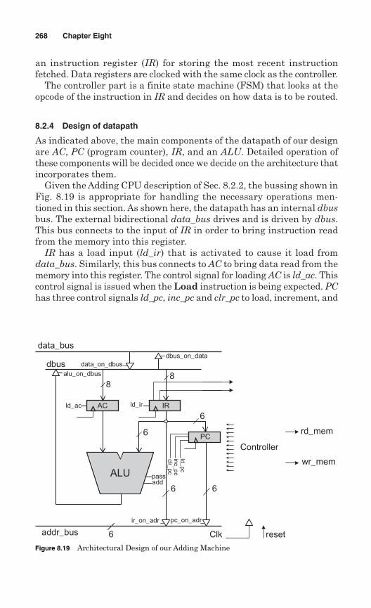
an instruction register (IR) for storing the most recent instructionfetched. Data registers are clocked with the same clock as the controller.
The controller part is a finite state machine (FSM) that looks at theopcode of the instruction in IR and decides on how data is to be routed.
8.2.4 Design of datapath
As indicated above, the main components of the datapath of our designare AC, PC (program counter), IR, and an ALU. Detailed operation ofthese components will be decided once we decide on the architecture thatincorporates them.
Given the Adding CPU description of Sec. 8.2.2, the bussing shown inFig. 8.19 is appropriate for handling the necessary operations men-tioned in this section. As shown here, the datapath has an internal dbusbus. The external bidirectional data_bus drives and is driven by dbus.This bus connects to the input of IR in order to bring instruction readfrom the memory into this register.
IR has a load input (ld_ir) that is activated to cause it load fromdata_bus. Similarly, this bus connects to AC to bring data read from thememory into this register. The control signal for loading AC is ld_ac. Thiscontrol signal is issued when the Load instruction is being expected. PChas three control signals ld_pc, inc_pc and clr_pc to load, increment, and
268 Chapter Eight
AC
PC
IR
ALU
Controller
Clk reset
rd_mem
wr_mem
6
6
6
88
pass
6
addr_bus
dbus
6
ld_pcin
c_pc
clr_pc
ld_irld_ac
add
dbus_on_datadata_on_dbus
data_bus
pc_on_adrir_on_adr
alu_on_dbus
Figure 8.19 Architectural Design of our Adding Machine
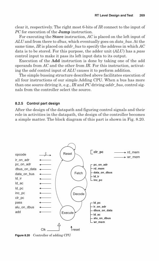
clear it, respectively. The right most 6-bits of IR connect to the input ofPC for execution of the Jump instruction.
For executing the Store instruction, AC is placed on the left input ofALU and from there to dbus, which eventually goes on data_bus. At thesame time, IR is placed on addr_bus to specify the address in which ACdata is to be stored. For this purpose, the adder unit (ALU ) has a passcontrol input to make it pass its left input data to its output.
Execution of the Add instruction is done by taking one of the addoperands from AC and the other from IR. For this instruction, activat-ing the add control input of ALU causes it to perform addition.
The simple bussing structure described above facilitates execution ofall four instructions of our simple Adding CPU. When a bus has morethan one source driving it, e.g., IR and PC driving addr_bus, control sig-nals from the controller select the source.
8.2.5 Control part design
After the design of the datapath and figuring control signals and theirrole in activities in the datapath, the design of the controller becomesa simple matter. The block diagram of this part is shown in Fig. 8.20.
RT Level Design and Test 269
2opcode
ir_on_adrpc_on_adrdbus_on_data
data_on_busld_irld_ac
ld_pcinc_pcclr_pcpass alu_on_dbus
Reset
Clk
clr_pc
Fetch
pc_on_adrrd_memdata_on_dbusld_irinc_pc
Decode
Execute
ir_on_adrdbus_on_data
ld_acalu_on_dbuswr_mem
ld_pc
add
rd_memwr_mem
reset
Figure 8.20 Controller of adding CPU
The controller of our simple von Neumann machine has four states,Reset, Fetch, Decode, and Execute. As the machine cycles through thesestates, various control signals are issued. In state Reset, for example,the clr_pc control signal is issued. State Fetch issues pc_on_adr, rd_mem,data_on_dbus, ld_ir, and inc_pc, to read memory from the present PClocation, route it to IR, load it into IR, and increment PC for the nextmemory fetch. Depending on opcode bits, that are the controller inputs,the Execute state of the controller issues control signals for execution ofLoad, Store, Add, and Jump instructions. The next section discussesdetails of the controller signals and their role in execution of theseinstructions.
8.2.6 AddingCPU Verilog description
We develop the complete Verilog code of our simple adding machine bydeveloping code for the blocks of Fig. 8.19. We first describe componentsof the datapath, and then will form the Verilog code of the datapath byinstantiating and wiring these components. The controller will bedescribed next, using a state machine coding style. At the end, thedescription of our small von Neumann example will be completed bywiring datapath and controller in a top-level Verilog module.
8.2.6.1 Data components. Datapath components of AddingCPU couldbe described by always and assign statements directly in the datapathdescription of the machine. Recall that this coding technique was usedfor the multiplier example of the previous section. However, in thisexample we are taking a more general and extendable approach. Wedescribe our components so that they can be independently simulatedand tested. This is necessary for large designs with more complex com-ponents. The approach presented here will be used in describing ourlarger machine in the next section. Verilog code for PC, AC, IR, and ALUmodules are shown in Fig. 8.21.
Accumulator (AC) and instruction register (IR) are simple registerswith load enable control inputs. These inputs are driven by control sig-nals coming from the controller through datapath ports. The programcounter (PC) is a counter with parallel load, increment, and clear capa-bilities. As shown, this component has three control signals to controlits functionality. The ALU (the last module in Fig. 8.21) is a combina-tional logic with pass and add control inputs. If pass is 1, the a inputgoes on the output, and if add is 1, the ALU output becomes the sum ofa and b.
Codings presented for AC, IR, PC, and ALU are synthesizable andindividually testable. These parts are instantiated in the datapath of ourmachine.
270 Chapter Eight
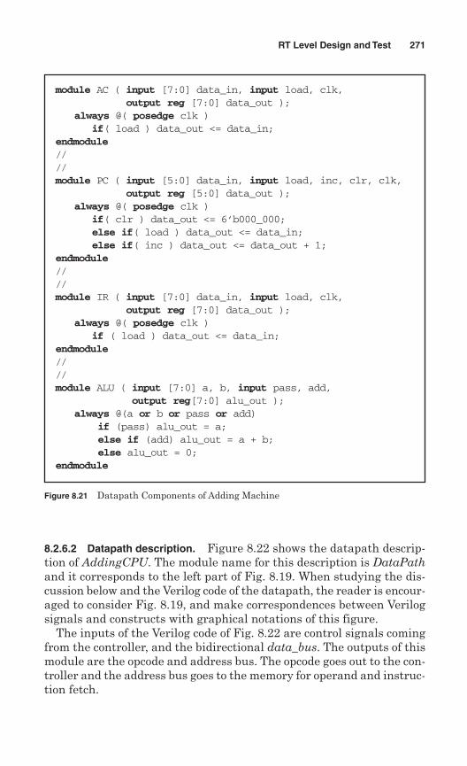
8.2.6.2 Datapath description. Figure 8.22 shows the datapath descrip-tion of AddingCPU. The module name for this description is DataPathand it corresponds to the left part of Fig. 8.19. When studying the dis-cussion below and the Verilog code of the datapath, the reader is encour-aged to consider Fig. 8.19, and make correspondences between Verilogsignals and constructs with graphical notations of this figure.
The inputs of the Verilog code of Fig. 8.22 are control signals comingfrom the controller, and the bidirectional data_bus. The outputs of thismodule are the opcode and address bus. The opcode goes out to the con-troller and the address bus goes to the memory for operand and instruc-tion fetch.
RT Level Design and Test 271
Figure 8.21 Datapath Components of Adding Machine
module AC ( input [7:0] data_in, input load, clk, output reg [7:0] data_out );
always @( posedge clk )if( load ) data_out <= data_in;
endmodule////module PC ( input [5:0] data_in, input load, inc, clr, clk,
output reg [5:0] data_out );always @( posedge clk )
if( clr ) data_out <= 6’b000_000;else if( load ) data_out <= data_in;else if( inc ) data_out <= data_out + 1;
endmodule////module IR ( input [7:0] data_in, input load, clk,
output reg [7:0] data_out );always @( posedge clk )
if ( load ) data_out <= data_in;endmodule////module ALU ( input [7:0] a, b, input pass, add,
output reg[7:0] alu_out );always @(a or b or pass or add)
if (pass) alu_out = a;else if (add) alu_out = a + b;else alu_out = 0;
endmodule
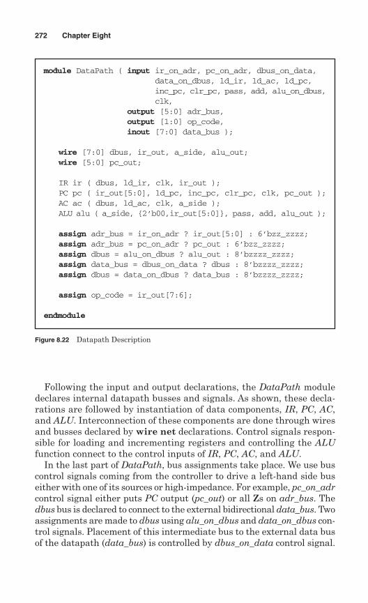
Following the input and output declarations, the DataPath moduledeclares internal datapath busses and signals. As shown, these decla-rations are followed by instantiation of data components, IR, PC, AC,and ALU. Interconnection of these components are done through wiresand busses declared by wire net declarations. Control signals respon-sible for loading and incrementing registers and controlling the ALUfunction connect to the control inputs of IR, PC, AC, and ALU.
In the last part of DataPath, bus assignments take place. We use buscontrol signals coming from the controller to drive a left-hand side buseither with one of its sources or high-impedance. For example, pc_on_adrcontrol signal either puts PC output (pc_out) or all Zs on adr_bus. Thedbus bus is declared to connect to the external bidirectional data_bus. Twoassignments are made to dbus using alu_on_dbus and data_on_dbus con-trol signals. Placement of this intermediate bus to the external data busof the datapath (data_bus) is controlled by dbus_on_data control signal.
272 Chapter Eight
Figure 8.22 Datapath Description
module DataPath ( input ir_on_adr, pc_on_adr, dbus_on_data, data_on_dbus, ld_ir, ld_ac, ld_pc, inc_pc, clr_pc, pass, add, alu_on_dbus,clk,
output [5:0] adr_bus, output [1:0] op_code, inout [7:0] data_bus );
wire [7:0] dbus, ir_out, a_side, alu_out;wire [5:0] pc_out;
IR ir ( dbus, ld_ir, clk, ir_out );PC pc ( ir_out[5:0], ld_pc, inc_pc, clr_pc, clk, pc_out );AC ac ( dbus, ld_ac, clk, a_side ); ALU alu ( a_side, {2’b00,ir_out[5:0]}, pass, add, alu_out );
assign adr_bus = ir_on_adr ? ir_out[5:0] : 6’bzz_zzzz;assign adr_bus = pc_on_adr ? pc_out : 6’bzz_zzzz;assign dbus = alu_on_dbus ? alu_out : 8’bzzzz_zzzz;assign data_bus = dbus_on_data ? dbus : 8’bzzzz_zzzz;assign dbus = data_on_dbus ? data_bus : 8’bzzzz_zzzz;
assign op_code = ir_out[7:6];
endmodule
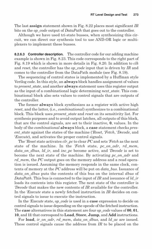
The last assign statement shown in Fig. 8.22 places most significant IRbits on the op_code output of DataPath that goes out to the controller.
Although we have used tri-state busses, when synthesizing this cir-cuit, we can direct our synthesis tool to use AND-OR logic or multi-plexers to implement these busses.
8.2.6.3 Controller description. The controller code for our adding machineexample is shown in Fig. 8.23. This code corresponds to the right part ofFig. 8.19 which is shown in more details in Fig. 8.20. In addition to clkand reset, the controller has the op_code input that is driven by IR andcomes to the controller from the DataPath module (see Fig. 8.19).
The sequencing of control states is implemented by a Huffman styleVerilog code. In this style, an always block handles assignment of valuesto present_state, and another always statement uses this register outputas the input of a combinational logic determining next_state. This com-binational block also sets values to control signals that are outputs ofthe controller.
The former always block synthesizes as a register with active highreset, and the latter, (i.e., combinational) synthesizes to a combinationalblock. This block uses present_state and reset on its sensitivity list. Forsynthesis purposes and to avoid output latches, all outputs of this block,that are the control signals, are set to their inactive, 0, values. In thebody of the combinational always block, a case statement checks pres-ent_state against the states of the machine (‘Reset, ‘Fetch, ‘Decode, and‘Execute), and activates the proper control signals.
The ‘Reset state activates clr_pc to clear PC and sets ‘Fetch as the nextstate of the machine. In the ‘Fetch state, pc_on_adr, rd_mem,data_on_dbus, ld_ir, and inc_pc become active, and ‘Decode is set tobecome the next state of the machine. By activating pc_on_adr andrd_mem, the PC output goes on the memory address and a read opera-tion is issued. Assuming the memory responds in the same clock, con-tents of memory at the PC address will be put on data_bus. Issuance ofdata_on_dbus puts the contents of this bus on the internal dbus ofDataPath. This bus is connected to the input of IR and issuance of ld_irloads its contents into this register. The next state of the controller is‘Decode that makes the new contents of IR available for the controller.In the ‘Execute state a newly fetched instruction in IR decides on con-trol signals to issue to execute the instruction.
In the ‘Execute state, op_code is used in a case expression to decide oncontrol signals to issue depending on the opcode of the fetched instruction.The case alternatives in this statement are four op_code values of 00, 01,10, and 11 that correspond to Load, Store, Jump, and Add instructions.
For load, ir_on_adr, rd_mem, data_on_dbus, and ld_ac are issued.These control signals cause the address from IR to be placed on the
RT Level Design and Test 273
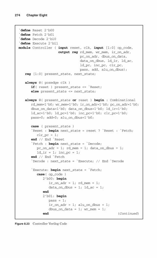
274 Chapter Eight
Figure 8.23 Controller Verilog Code
`define Reset 2’b00`define Fetch 2’b01`define Decode 2’b10`define Execute 2’b11module Controller ( input reset, clk, input [1:0] op_code,
output reg rd_mem, wr_mem, ir_on_adr,pc_on_adr, dbus_on_data,data_on_dbus, ld_ir, ld_ac,ld_pc, inc_pc, clr_pc,pass, add, alu_on_dbus);
reg [1:0] present_state, next_state;
always @( posedge clk ) if( reset ) present_state <= `Reset;else present_state <= next_state;
always @( present_state or reset ) begin : Combinationalrd_mem=1’b0; wr_mem=1’b0; ir_on_adr=1’b0; pc_on_adr=1’b0;dbus_on_data=1’b0; data_on_dbus=1’b0; ld_ir=1’b0;ld_ac=1’b0; ld_pc=1’b0; inc_pc=1’b0; clr_pc=1’b0;pass=0; add=0; alu_on_dbus=1’b0;
case ( present_state )`Reset : begin next_state = reset ? `Reset : `Fetch;
clr_pc = 1;end // End `Reset`Fetch : begin next_state = `Decode;
pc_on_adr = 1; rd_mem = 1; data_on_dbus = 1; ld_ir = 1; inc_pc = 1;
end // End `Fetch`Decode : next_state = `Execute; // End `Decode
`Execute: begin next_state = `Fetch;case( op_code )
2’b00: beginir_on_adr = 1; rd_mem = 1;data_on_dbus = 1; ld_ac = 1;
end2’b01: begin
pass = 1;ir_on_adr = 1; alu_on_dbus = 1;dbus_on_data = 1; wr_mem = 1;
end (Continued)
addr_bus address bus, memory read to take place, and data frommemory to be loaded into AC. Data from the memory come throughdata_bus onto dbus of DataPath by the control signal data_on_dbus.
Controller executes the Store instruction by issuing pass, ir_on_adr,alu_on_dbus, dbus_on_data, and wr_mem. As shown in Fig. 8.19, thesesignals take contents of AC to the input bus of the memory (i.e.,data_bus), and wr_mem causes the writing into the memory to takeplace. Note that pass causes AC to pass through ALU unchanged.
The Jump instruction is executed by enabling PC load input, whichtakes the jump address from IR (see Fig. 8.19).
The last instruction of this machine is Add, for execution of which,add, alu_on_dbus, and ld_ac are issued. This instruction adds data inthe upper six bits of IR with AC and loads the result into AC. The addcontrol signal instructs ALU to add its two inputs; the alu_on_dbusputs this output on the internal datapath dbus; and the ld_ac causes ACto be loaded with the result of addition.
8.2.6.4 The complete machine. The top-level module for our addingmachine example is shown in Fig. 8.24. In the AddingCPU moduleshown, DataPath and Controller modules are instantiated. Port con-nections of the Controller include its output control signals, the opcodeinput from DataPath and the reset external input. Port connections ofDataPath consist of adr_bus and data_bus external busses, opcodeoutput, and control signal inputs.
8.2.7 Testing adding CPU
In the testbench for the AddingCPU module, we model a simple memorywith read and write operations. The memory is file-based and we will
RT Level Design and Test 275
Figure 8.23 Controller Verilog Code (Continued)
2’b10: ld_pc = 1;2’b11: begin
add = 1; alu_on_dbus = 1; ld_ac = 1;end
endcaseend // End `Executedefault : next_state = `Reset;
endcaseend
endmodule
use file I/O tasks for reading and writing from and to the memory. Tomake this testbench more complete, we use a task for converting instruc-tions in mnemonic form from an external file to binary memory data.In general, memory modeling and file I/O are elaborated in the testbenchof AddingCPU.
8.2.7.1 Testbench outline. The outline of the testbench is shown inFig. 8.25. This module reads the InstructionFile.mem file which containsinstruction mnemonics and their addresses, converts them to hex andwrites them to HexadecimalFile.mem file. After this conversion is done,every addressed memory read or write uses the hex file. Because the unitunder test (UUT) does not have a large memory, all read and write oper-ations are directly performed on the HexadecimalFile.mem file, and noimage of its memory is kept in the testbench as a fast buffer as an arrayof reg. The processor of the next section uses such a memory bufferingscheme for faster memory input-output operations.
As shown in Fig. 8.25, after declarations and instantiation ofAddingCPU, an initial block calls the Convert task to read the instruc-tion file (InstructionFile.mem), translate instruction mnemonics to hex,and write hex data in the HexadecimalFile.mem file. Following the invo-cation of Convert, the testbench opens the HexadecimalFile.mem file for
276 Chapter Eight
Figure 8.24 Adding CPU Top-Level Module
module AddingCPU (input reset, clk, output [5:0] adr_bus, output rd_mem, wr_mem, inout [7:0] data_bus);
wire ir_on_adr, pc_on_adr, dbus_on_data, data_on_dbus,ld_ir,ld_ac, ld_pc, inc_pc, clr_pc, pass, add, alu_on_dbus;
wire [1:0] op_code;
Controller cu ( reset, clk, op_code, rd_mem, wr_mem, ir_on_adr,pc_on_adr, dbus_on_data, data_on_dbus, ld_ir,ld_ac, ld_pc, inc_pc, clr_pc, pass,add, alu_on_dbus );
DataPath dp ( ir_on_adr, pc_on_adr, dbus_on_data, data_on_dbus,ld_ir, ld_ac, ld_pc, inc_pc, clr_pc, pass, add,alu_on_dbus, clk, adr_bus, op_code, data_bus );
endmodule
read and write, and sets the end of the simulation run time. The $fopentask opens this hex file and assigns the HexFile descriptor that is adeclared integer to it. The $fclose task closes this file just before thesimulation run is stopped.
This initial block is followed by the Memory_Read_Write always block.This block assumes 64 8-bit hex data are available in HexadecimalFile.mem.For accessing this file, its descriptor HexFile, will be used.
Figure 8.26 shows the details of Memory_Read_Write always block.After a short delay (1 ns) after the posedge of clk, rd_mem and wr_memare expected to be stable. At this time, if rd_mem is 1, data on adr_bus
RT Level Design and Test 277
Figure 8.25 Outline of Adding CPU Testbench
module Test_AddingCPU;reg reset=1, clk=0;wire [5:0] adr_bus;wire rd_mem, wr_mem;wire [7:0] data_bus; reg [7:0] mem_data=8’b0; reg control=0;integer HexFile, check;
AddingCPU UUT (reset, clk, adr_bus, rd_mem, wr_mem, data_bus);
always #10 clk = ~clk;
initial beginConvert;HexFile = $fopen (“HexadecimalFile.mem”, “r+”);#25 reset=1’b0;#405 $fclose (HexFile);$stop;
end
always @(posedge clk) begin : Memory_Read_Write// . . .
end
// . . .
task Convert;// . . .
endtaskendmodule
is used to set the position of the next read from HexFile. Since data inHexadecimalFile.mem are in hex (2 bytes), a total of 4 bytes that includetwo “end of line” bytes are used for each memory entry. Therefore,$fseek of Fig. 8.26 positions the next reading from 4*adr_bus. The$fscanf task that follows this task reads the hex data at the file posi-tion into mem_data. This variable is local to the testbench and is puton data_bus only when reading from the memory is to take place. Thecontrol variable is used to drive data_bus with mem_data or 8’hZZ.
The next part of the always block of Fig. 8.26 handles writing intothe memory. For this purpose, after file positioning, the $fwrite taskwrites contents of data_bus into HexadecimalFile.mem. After everywriting $fflush writes any buffered output to this file.
The testbench outline of Fig. 8.25 shows the convert task that isused for converting instruction mnemonics of InstructionFile.memto hex data in HexadecimalFile.mem. Figure 8.27 shows six lines ofInstructionFile.mem and its corresponding hex translation in memorylocations 0 to 15.
The Convert task reads a line of InstructionFile.mem that contains amemory location, its mnemonic, and the instruction operand. This taskconverts this line to an opcode and its data and writes it in its specifiedlocation in HexadecimalFile.mem. For example, the third line of the
278 Chapter Eight
Figure 8.26 Memory Read and Write
always @(posedge clk) begin : Memory_Read_Writecontrol = 0;#1;if (rd_mem) begin
#1;check = $fseek (HexFile, 4 * adr_bus, 0);check = $fscanf (HexFile, “%h”, mem_data);control = 1;
endif (wr_mem) begin
#1;check = $fseek (HexFile, 4 * adr_bus, 0);$fwrite (HexFile, “%h”, data_bus);$fflush (HexFile);
endend
assign data_bus = (control) ? mem_data: 8’hZZ;
instruction file of Fig. 8.27 (sta 0A) is translated to 4A and is put in loca-tion 1 of the hexadecimal file. For direct memory data, the instructionfile uses the “:::” notation. 0F ::: 0f shown in Fig. 8.27 is translated todata 0f in location 15 of the hexadecimal file.
The Convert task is shown in Fig. 8.28. Initially all locations ofHexadecimalFile.mem are initialized to “00”. The InstructionFile.memis opened for reading, (i.e., with r argument), and HexadecimalFile.memis opened for reading and writing, (i.e., with r+ argument) file descrip-tors for these two files are InstFile and HexFile, respectively.
Convert has a while loop that reads data from InstFile, converts it tohex and puts it in its corresponding location in HexFile. The $fscanf task,shown in this while, reads the first two hex digits of a line of instruc-tion into addr. This variable is then used for setting the write positionfor the HexFile file. This file positioning is done by $fseek. This is fol-lowed by $fgets that reads the opcode string from the instruction file(InstFile). A case statement in Convert translates string opcodes to theirhex equivalent, and an $fwrite task writes this hex data into the hexfile (HexFile) at the location set by the $fseek task.
If the opcode string read from InstFile is “:::”, the hex data that fol-lows this string will be written into HexFile location specified by addr.The last part of Convert flushes HexFile and closes both instruction andhexadecimal files.
The testbench discussed above tests AddingCPU for all its instruc-tions. This example shows the power and flexibility of Verilog file han-dling tasks for testbench development. In modeling larger memories,
RT Level Design and Test 279
InstructionFile HexadecimalFile
Line: Location: 1: 00 lda 0f 00: 0F 2: 0f ::: 0f 01: 4A 3: 01 sta 0a 02: C1 4: 02 add 01 03: 4B 5: 03 sta 0b 04: 80 6: 04 jmp 00 06: 00 07: 00 08: 00 09: 00 10: 00 11: 00 12: 00 13: 00 14: 00
15: 0F
Figure 8.27 Instruction Mnemonics and Hex Memory Data
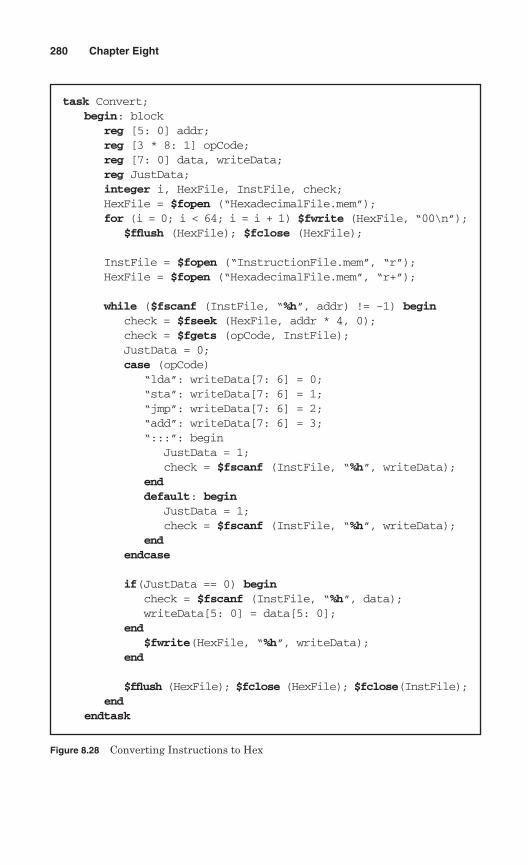
280 Chapter Eight
Figure 8.28 Converting Instructions to Hex
task Convert;begin: block
reg [5: 0] addr;reg [3 * 8: 1] opCode;reg [7: 0] data, writeData;reg JustData;integer i, HexFile, InstFile, check;HexFile = $fopen (“HexadecimalFile.mem”);for (i = 0; i < 64; i = i + 1) $fwrite (HexFile, “00\n”);
$fflush (HexFile); $fclose (HexFile);
InstFile = $fopen (“InstructionFile.mem”, “r”);HexFile = $fopen (“HexadecimalFile.mem”, “r+”);
while ($fscanf (InstFile, “%h”, addr) != -1) begincheck = $fseek (HexFile, addr * 4, 0);check = $fgets (opCode, InstFile);JustData = 0;case (opCode)
“lda”: writeData[7: 6] = 0;“sta”: writeData[7: 6] = 1;“jmp”: writeData[7: 6] = 2;“add”: writeData[7: 6] = 3;“:::”: begin
JustData = 1;check = $fscanf (InstFile, “%h”, writeData);
enddefault: begin
JustData = 1;check = $fscanf (InstFile, “%h”, writeData);
endendcase
if(JustData == 0) begincheck = $fscanf (InstFile, “%h”, data);writeData[5: 0] = data[5: 0];
end$fwrite(HexFile, “%h”, writeData);
end
$fflush (HexFile); $fclose (HexFile); $fclose(InstFile);end
endtask
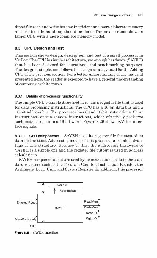
direct file read and write become inefficient and more elaborate memoryand related file handling should be done. The next section shows alarger CPU with a more complete memory model.
8.3 CPU Design and Test
This section shows design, description, and test of a small processor inVerilog. The CPU is simple architecture, yet enough hardware (SAYEH)that has been designed for educational and benchmarking purposes.The design is simple, and follows the design strategy used for the AddingCPU of the previous section. For a better understanding of the materialpresented here, the reader is expected to have a general understandingof computer architectures.
8.3.1 Details of processor functionality
The simple CPU example discussed here has a register file that is usedfor data processing instructions. The CPU has a 16-bit data bus and a16-bit address bus. The processor has 8 and 16-bit instructions. Shortinstructions contain shadow instructions, which effectively pack twosuch instructions into a 16-bit word. Figure 8.29 shows SAYEH inter-face signals.
8.3.1.1 CPU components. SAYEH uses its register file for most of itsdata instructions. Addressing modes of this processor also take advan-tage of this structure. Because of this, the addressing hardware ofSAYEH is a simple one and the register file output is used in addresscalculations.
SAYEH components that are used by its instructions include the stan-dard registers such as the Program Counter, Instruction Register, theArithmetic Logic Unit, and Status Register. In addition, this processor
RT Level Design and Test 281
SAYEH
Databus
Addressbus
ReadMem
WriteMem
ReadIO
WriteIO
ExternalReset
MemDataready
Clk
Figure 8.29 SAYEH Interface
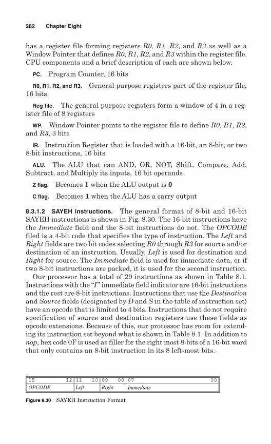
has a register file forming registers R0, R1, R2, and R3 as well as aWindow Pointer that defines R0, R1, R2, and R3 within the register file.CPU components and a brief description of each are shown below.
PC. Program Counter, 16 bits
R0, R1, R2, and R3. General purpose registers part of the register file,16 bits
Reg file. The general purpose registers form a window of 4 in a reg-ister file of 8 registers
WP. Window Pointer points to the register file to define R0, R1, R2,and R3, 3 bits
IR. Instruction Register that is loaded with a 16-bit, an 8-bit, or two8-bit instructions, 16 bits
ALU. The ALU that can AND, OR, NOT, Shift, Compare, Add,Subtract, and Multiply its inputs, 16 bit operands
Z flag. Becomes 1 when the ALU output is 0
C flag. Becomes 1 when the ALU has a carry output
8.3.1.2 SAYEH instructions. The general format of 8-bit and 16-bitSAYEH instructions is shown in Fig. 8.30. The 16-bit instructions havethe Immediate field and the 8-bit instructions do not. The OPCODEfiled is a 4-bit code that specifies the type of instruction. The Left andRight fields are two bit codes selecting R0 through R3 for source and/ordestination of an instruction. Usually, Left is used for destination andRight for source. The Immediate field is used for immediate data, or iftwo 8-bit instructions are packed, it is used for the second instruction.
Our processor has a total of 29 instructions as shown in Table 8.1.Instructions with the “I ” immediate field indicator are 16-bit instructionsand the rest are 8-bit instructions. Instructions that use the Destinationand Source fields (designated by D and S in the table of instruction set)have an opcode that is limited to 4 bits. Instructions that do not requirespecification of source and destination registers use these fields asopcode extensions. Because of this, our processor has room for extend-ing its instruction set beyond what is shown in Table 8.1. In addition tonop, hex code 0F is used as filler for the right most 8-bits of a 16-bit wordthat only contains an 8-bit instruction in its 8 left-most bits.
282 Chapter Eight
15 12 11 10 09 08 07 00
ImmediateOPCODE Left Right
Figure 8.30 SAYEH Instruction Format
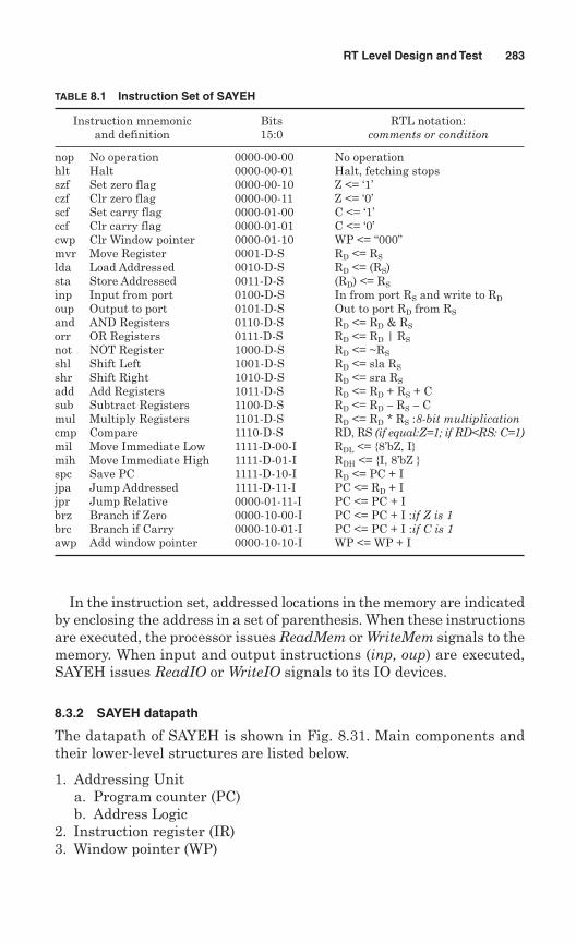
In the instruction set, addressed locations in the memory are indicatedby enclosing the address in a set of parenthesis. When these instructionsare executed, the processor issues ReadMem or WriteMem signals to thememory. When input and output instructions (inp, oup) are executed,SAYEH issues ReadIO or WriteIO signals to its IO devices.
8.3.2 SAYEH datapath
The datapath of SAYEH is shown in Fig. 8.31. Main components andtheir lower-level structures are listed below.
1. Addressing Unita. Program counter (PC)b. Address Logic
2. Instruction register (IR)3. Window pointer (WP)
RT Level Design and Test 283
TABLE 8.1 Instruction Set of SAYEH
Instruction mnemonic Bits RTL notation:and definition 15:0 comments or condition
nop No operation 0000-00-00 No operationhlt Halt 0000-00-01 Halt, fetching stopsszf Set zero flag 0000-00-10 Z <= ‘1’czf Clr zero flag 0000-00-11 Z <= ‘0’scf Set carry flag 0000-01-00 C <= ‘1’ccf Clr carry flag 0000-01-01 C <= ‘0’cwp Clr Window pointer 0000-01-10 WP <= “000”mvr Move Register 0001-D-S RD <= RS
lda Load Addressed 0010-D-S RD <= (RS)sta Store Addressed 0011-D-S (RD) <= RS
inp Input from port 0100-D-S In from port RS and write to RD
oup Output to port 0101-D-S Out to port RD from RS
and AND Registers 0110-D-S RD <= RD & RS
orr OR Registers 0111-D-S RD <= RD | RS
not NOT Register 1000-D-S RD <= ~RS
shl Shift Left 1001-D-S RD <= sla RS
shr Shift Right 1010-D-S RD <= sra RS
add Add Registers 1011-D-S RD <= RD + RS + Csub Subtract Registers 1100-D-S RD <= RD − RS − Cmul Multiply Registers 1101-D-S RD <= RD * RS :8-bit multiplicationcmp Compare 1110-D-S RD, RS (if equal:Z=1; if RD<RS: C=1)mil Move Immediate Low 1111-D-00-I RDL <= {8’bZ, I}mih Move Immediate High 1111-D-01-I RDH <= {I, 8’bZ }spc Save PC 1111-D-10-I RD <= PC + Ijpa Jump Addressed 1111-D-11-I PC <= RD + Ijpr Jump Relative 0000-01-11-I PC <= PC + Ibrz Branch if Zero 0000-10-00-I PC <= PC + I :if Z is 1brc Branch if Carry 0000-10-01-I PC <= PC + I :if C is 1awp Add window pointer 0000-10-10-I WP <= WP + I
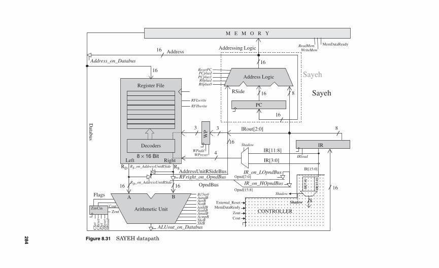
M E M O R Y
PC
IR
WP
Flags
Databus
3/
/ 8
/8
/ 16
/16
/ 16
16/
16/
/16
3/
CONTROLLER
8/
/ 16
16
/ 16
Addressing Logic
4/
Address_on_Databus
ALUout_on_Databus
RFright_on_OpndBusIR_on_LOpndBus
ResetPCPCplusIPCplus1R0plusI
IRload
WPaddWPreset
ZR
eset
RFLwrite
Address
OpndBus
IRout[2:0]
ReadMemWriteMem
CoutZout Arithmetic Unit
Address Logic
Register File
8 × 16 Bit
CSe
tC
Res
etZ
Set
SRlo
ad
ZinCin
RD
A B
RightLeft
RD_on_AddressUnitRSide
RS_on_AddressUnitRSide
R0plus0
RFHwrite
RSide
B15to0AandB
ShrBAcmpBAmulBAsubBAaddBNotBAorB
ShlB
External_ResetMemDataReady
ZoutCout
Shadow
IR[11:8]
IR[3:0]
MemDataReady
Shadow
IR_on_HOpndBusOpnd[15:8]
Opnd[7:0]AddressUnitRSideBus
Decoders
IR[1
5:8]
IR[15:0]
Shadow
RS
IR[7
:0]
Sayeh
Sayeh
Figure 8.31 SAYEH datapath
284
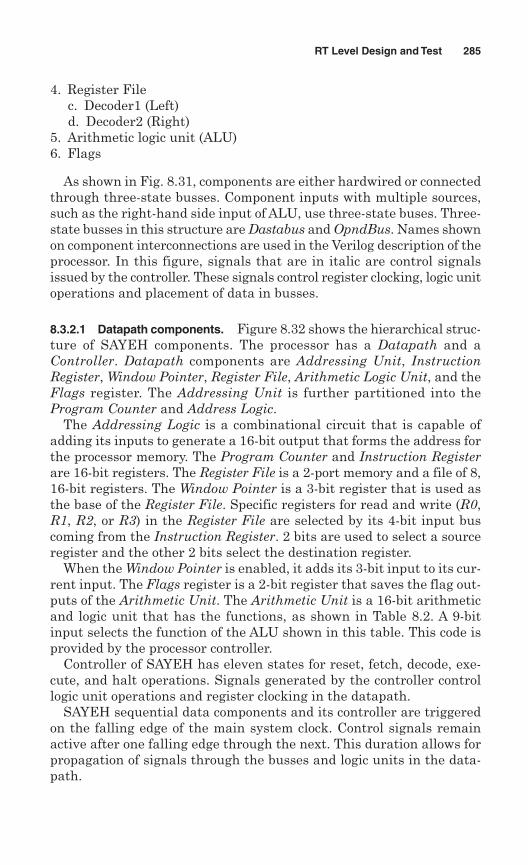
4. Register Filec. Decoder1 (Left)d. Decoder2 (Right)
5. Arithmetic logic unit (ALU)6. Flags
As shown in Fig. 8.31, components are either hardwired or connectedthrough three-state busses. Component inputs with multiple sources,such as the right-hand side input of ALU, use three-state buses. Three-state busses in this structure are Dastabus and OpndBus. Names shownon component interconnections are used in the Verilog description of theprocessor. In this figure, signals that are in italic are control signalsissued by the controller. These signals control register clocking, logic unitoperations and placement of data in busses.
8.3.2.1 Datapath components. Figure 8.32 shows the hierarchical struc-ture of SAYEH components. The processor has a Datapath and aController. Datapath components are Addressing Unit, InstructionRegister, Window Pointer, Register File, Arithmetic Logic Unit, and theFlags register. The Addressing Unit is further partitioned into theProgram Counter and Address Logic.
The Addressing Logic is a combinational circuit that is capable ofadding its inputs to generate a 16-bit output that forms the address forthe processor memory. The Program Counter and Instruction Registerare 16-bit registers. The Register File is a 2-port memory and a file of 8,16-bit registers. The Window Pointer is a 3-bit register that is used asthe base of the Register File. Specific registers for read and write (R0,R1, R2, or R3) in the Register File are selected by its 4-bit input buscoming from the Instruction Register. 2 bits are used to select a sourceregister and the other 2 bits select the destination register.
When the Window Pointer is enabled, it adds its 3-bit input to its cur-rent input. The Flags register is a 2-bit register that saves the flag out-puts of the Arithmetic Unit. The Arithmetic Unit is a 16-bit arithmeticand logic unit that has the functions, as shown in Table 8.2. A 9-bitinput selects the function of the ALU shown in this table. This code isprovided by the processor controller.
Controller of SAYEH has eleven states for reset, fetch, decode, exe-cute, and halt operations. Signals generated by the controller controllogic unit operations and register clocking in the datapath.
SAYEH sequential data components and its controller are triggeredon the falling edge of the main system clock. Control signals remainactive after one falling edge through the next. This duration allows forpropagation of signals through the busses and logic units in the data-path.
RT Level Design and Test 285
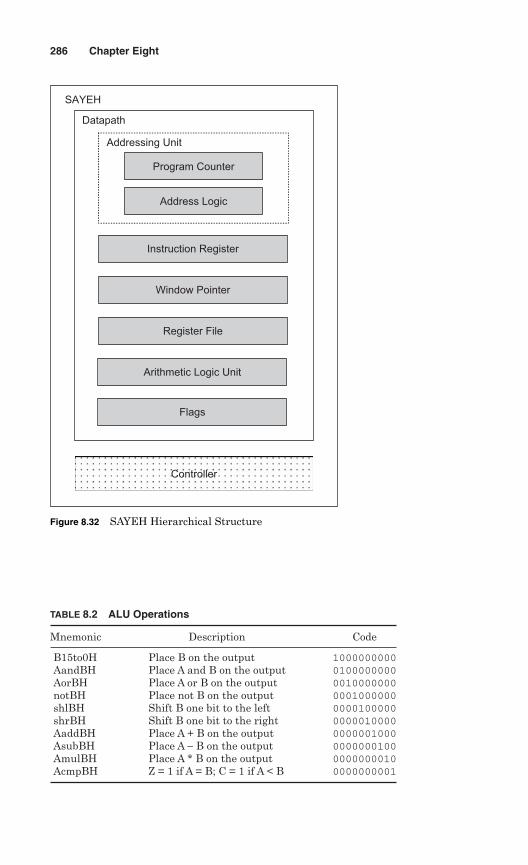
286 Chapter Eight
TABLE 8.2 ALU Operations
Mnemonic Description Code
B15to0H Place B on the output 1000000000AandBH Place A and B on the output 0100000000AorBH Place A or B on the output 0010000000notBH Place not B on the output 0001000000shlBH Shift B one bit to the left 0000100000shrBH Shift B one bit to the right 0000010000AaddBH Place A + B on the output 0000001000AsubBH Place A − B on the output 0000000100AmulBH Place A * B on the output 0000000010AcmpBH Z = 1 if A = B; C = 1 if A < B 0000000001
SAYEH
Datapath
Addressing Unit
Instruction Register
Window Pointer
Register File
Arithmetic Logic Unit
Flags
Address Logic
Program Counter
Controller
Figure 8.32 SAYEH Hierarchical Structure
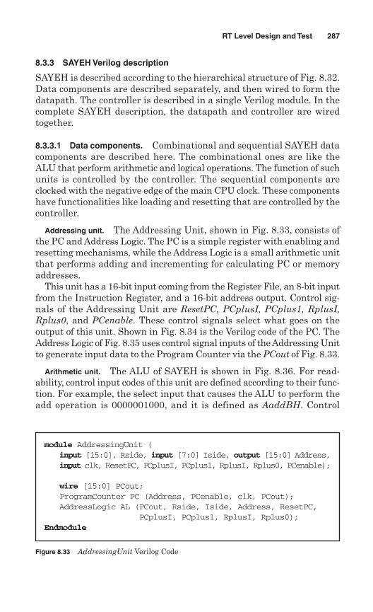
8.3.3 SAYEH Verilog description
SAYEH is described according to the hierarchical structure of Fig. 8.32.Data components are described separately, and then wired to form thedatapath. The controller is described in a single Verilog module. In thecomplete SAYEH description, the datapath and controller are wiredtogether.
8.3.3.1 Data components. Combinational and sequential SAYEH datacomponents are described here. The combinational ones are like theALU that perform arithmetic and logical operations. The function of suchunits is controlled by the controller. The sequential components areclocked with the negative edge of the main CPU clock. These componentshave functionalities like loading and resetting that are controlled by thecontroller.
Addressing unit. The Addressing Unit, shown in Fig. 8.33, consists ofthe PC and Address Logic. The PC is a simple register with enabling andresetting mechanisms, while the Address Logic is a small arithmetic unitthat performs adding and incrementing for calculating PC or memoryaddresses.
This unit has a 16-bit input coming from the Register File, an 8-bit inputfrom the Instruction Register, and a 16-bit address output. Control sig-nals of the Addressing Unit are ResetPC, PCplusI, PCplus1, RplusI,Rplus0, and PCenable. These control signals select what goes on theoutput of this unit. Shown in Fig. 8.34 is the Verilog code of the PC. TheAddress Logic of Fig. 8.35 uses control signal inputs of the Addressing Unitto generate input data to the Program Counter via the PCout of Fig. 8.33.
Arithmetic unit. The ALU of SAYEH is shown in Fig. 8.36. For read-ability, control input codes of this unit are defined according to their func-tion. For example, the select input that causes the ALU to perform theadd operation is 0000001000, and it is defined as AaddBH. Control
RT Level Design and Test 287
Figure 8.33 AddressingUnit Verilog Code
module AddressingUnit (input [15:0], Rside, input [7:0] Iside, output [15:0] Address,input clk, ResetPC, PCplusI, PCplus1, RplusI, Rplus0, PCenable);
wire [15:0] PCout;ProgramCounter PC (Address, PCenable, clk, PCout);AddressLogic AL (PCout, Rside, Iside, Address, ResetPC,
PCplusI, PCplus1, RplusI, Rplus0);Endmodule
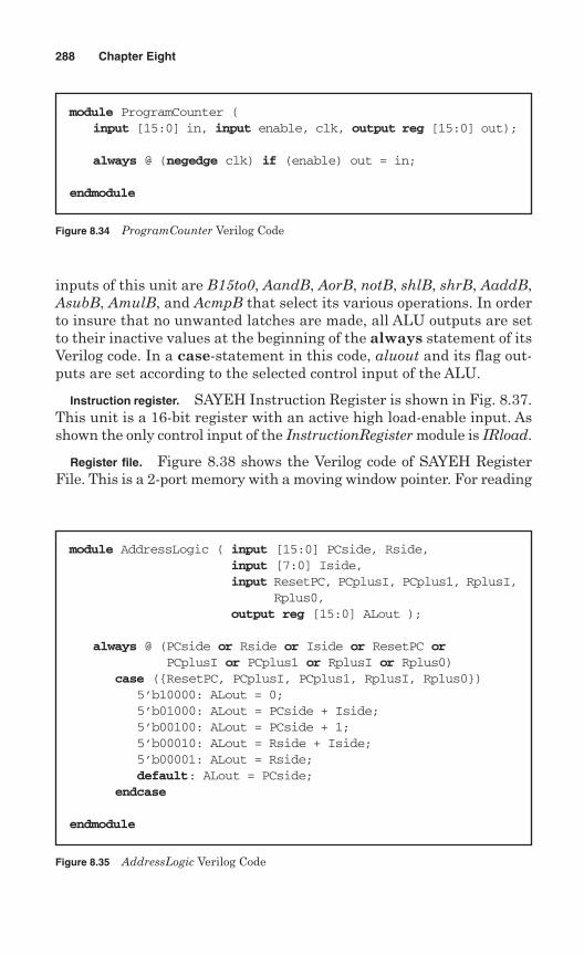
inputs of this unit are B15to0, AandB, AorB, notB, shlB, shrB, AaddB,AsubB, AmulB, and AcmpB that select its various operations. In orderto insure that no unwanted latches are made, all ALU outputs are setto their inactive values at the beginning of the always statement of itsVerilog code. In a case-statement in this code, aluout and its flag out-puts are set according to the selected control input of the ALU.
Instruction register. SAYEH Instruction Register is shown in Fig. 8.37.This unit is a 16-bit register with an active high load-enable input. Asshown the only control input of the InstructionRegister module is IRload.
Register file. Figure 8.38 shows the Verilog code of SAYEH RegisterFile. This is a 2-port memory with a moving window pointer. For reading
288 Chapter Eight
Figure 8.35 AddressLogic Verilog Code
module AddressLogic ( input [15:0] PCside, Rside, input [7:0] Iside,input ResetPC, PCplusI, PCplus1, RplusI,
Rplus0,output reg [15:0] ALout );
always @ (PCside or Rside or Iside or ResetPC orPCplusI or PCplus1 or RplusI or Rplus0)
case ({ResetPC, PCplusI, PCplus1, RplusI, Rplus0})5’b10000: ALout = 0;5’b01000: ALout = PCside + Iside;5’b00100: ALout = PCside + 1;5’b00010: ALout = Rside + Iside;5’b00001: ALout = Rside;default: ALout = PCside;
endcase
endmodule
Figure 8.34 ProgramCounter Verilog Code
module ProgramCounter ( input [15:0] in, input enable, clk, output reg [15:0] out);
always @ (negedge clk) if (enable) out = in;
endmodule
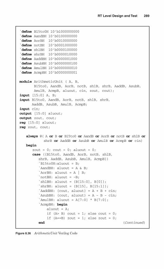
RT Level Design and Test 289
Figure 8.36 ArithmeticUnit Verilog Code
`define B15to0H 10’b1000000000`define AandBH 10’b0100000000`define AorBH 10’b0010000000`define notBH 10’b0001000000`define shlBH 10’b0000100000`define shrBH 10’b0000010000`define AaddBH 10’b0000001000`define AsubBH 10’b0000000100`define AmulBH 10’b0000000010`define AcmpBH 10’b0000000001
module ArithmeticUnit ( A, B, B15to0, AandB, AorB, notB, shlB, shrB, AaddB, AsubB, AmulB, AcmpB, aluout, cin, zout, cout);
input [15:0] A, B;input B15to0, AandB, AorB, notB, shlB, shrB,
AaddB, AsubB, AmulB, AcmpB;input cin;output [15:0] aluout;output zout, cout;reg [15:0] aluout;reg zout, cout;
always @( A or B or B15to0 or AandB or AorB or notB or shlB orshrB or AaddB or AsubB or AmulB or AcmpB or cin)
beginzout = 0; cout = 0; aluout = 0;case ({B15to0, AandB, AorB, notB, shlB,
shrB, AaddB, AsubB, AmulB, AcmpB})`B15to0H:aluout = B;`AandBH: aluout = A & B;`AorBH: aluout = A | B;`notBH: aluout = ~B;`shlBH: aluout = {B[15:0], B[0]};`shrBH: aluout = {B[15], B[15:1]};`AaddBH: {cout, aluout} = A + B + cin;`AsubBH: {cout, aluout} = A - B - cin;`AmulBH: aluout = A[7:0] * B[7:0];`AcmpBH: begin
aluout = A;if (A> B) cout = 1; else cout = 0;if (A==B) zout = 1; else zout = 0;
end (Continued)
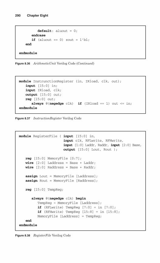
290 Chapter Eight
Figure 8.37 InstructionRegister Verilog Code
module InstrunctionRegister (in, IRload, clk, out);input [15:0] in;input IRload, clk;output [15:0] out;reg [15:0] out;
always @(negedge clk) if (IRload == 1) out <= in;endmodule
Figure 8.38 RegisterFile Verilog Code
module RegisterFile ( input [15:0] in,input clk, RFLwrite, RFHwrite,input [1:0] Laddr, Raddr, input [2:0] Base,output [15:0] Lout, Rout );
reg [15:0] MemoryFile [0:7];wire [2:0] Laddress = Base + Laddr;wire [2:0] Raddress = Base + Raddr;
assign Lout = MemoryFile [Laddress];assign Rout = MemoryFile [Raddress];
reg [15:0] TempReg;
always @(negedge clk) beginTempReg = MemoryFile [Laddress];if (RFLwrite) TempReg [7:0] = in [7:0];if (RFHwrite) TempReg [15:8] = in [15:8];MemoryFile [Laddress] = TempReg;
endendmodule
Figure 8.36 ArithmeticUnit Verilog Code (Continued)
default: aluout = 0;endcaseif (aluout == 0) zout = 1’b1;
end
endmodule
from the memory, the base of the window pointer (Base) is added to theleft and right addresses (Laddress and Raddress) and memory words areread on appropriate left and right outputs (Lout and Rout). Writing intothe memory is done in the location pointed by its left address (left is usedfor instruction destinations). The RFLwrite and RFHwrite control sig-nals decide whether a write is done to the low order or the high orderbits of the Register File. If both these signals are active, writing is donein a 16-bit word addressed by Laddress plus Base.
8.3.3.2 SAYEH datapath. Figure 8.39 shows the datapath of SAYEHmodule. This module specifies component instantiations and bussingstructure of the CPU according to the diagram of Fig. 8.31. Inputs of thismodule are the processor’s data and address busses, as well as controlsignals that are provided by the controller of the CPU. Control signalsshown in the DataPath module are routed to the instantiated data com-ponents or to the internal buses that are specified in this module.
Following the declarations, the DataPath module instantiatesAddressing Unit, Arithmetic Unit, Register File, Instruction Register,Status Register, and the Window Pointer. Control signals that are inputsof the DataPath are passed from this module to the data components viatheir port connections. For example, ResetPC that is an input ofDataPath and a control signal of AddressingUnit appears on the portlist of AddressingUnit in its instantiation statement.
The part that follows module instantiations makes bus assignments tothe internal buses of this module. For example, assignment of the outputof ArithmeticUnit to Databus that is controlled by ALU_on_Databus isdone by an assign statement with a right-hand side that is a conditionalexpression. Note the assignment of 16'bZZZZZZZZZZZZZZZZ to Databuswhen none of the control signals of this bus are active.
In the last part of the DataPath module, bits of IR that indicate sourceand destination registers to the Register File are placed on Laddr andRaddr inputs of this register. The Shadow signal becomes 1 if a shadowinstruction being executed is used to select appropriate bits of the IR assource and destination addresses.
8.3.3.3 SAYEH controller. The controller of SAYEH is a state machinewith nine states that issues appropriate control signals to the DataPath. The controller uses the Huffman style of coding, in which thestate machine has a large combinational part that is responsible for statetransitions and issuing controller outputs. State transitions are done bysetting next state values to the Nstate variable of reg type. Figure 8.40shows a general outline of this controller. Various sections of this out-line are discussed below.
RT Level Design and Test 291
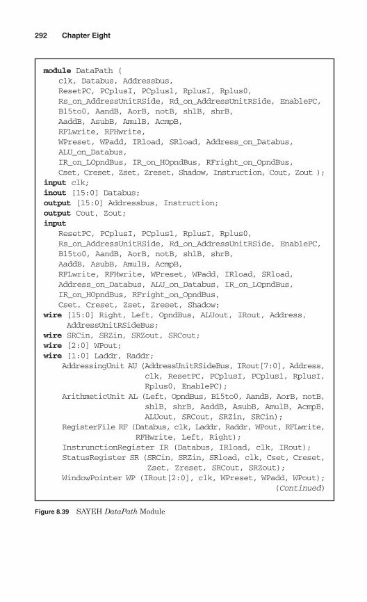
292 Chapter Eight
Figure 8.39 SAYEH DataPath Module
module DataPath ( clk, Databus, Addressbus, ResetPC, PCplusI, PCplus1, RplusI, Rplus0,Rs_on_AddressUnitRSide, Rd_on_AddressUnitRSide, EnablePC,B15to0, AandB, AorB, notB, shlB, shrB, AaddB, AsubB, AmulB, AcmpB, RFLwrite, RFHwrite,WPreset, WPadd, IRload, SRload, Address_on_Databus,ALU_on_Databus,IR_on_LOpndBus, IR_on_HOpndBus, RFright_on_OpndBus,Cset, Creset, Zset, Zreset, Shadow, Instruction, Cout, Zout );
input clk;inout [15:0] Databus;output [15:0] Addressbus, Instruction;output Cout, Zout;input
ResetPC, PCplusI, PCplus1, RplusI, Rplus0,Rs_on_AddressUnitRSide, Rd_on_AddressUnitRSide, EnablePC,B15to0, AandB, AorB, notB, shlB, shrB, AaddB, AsubB, AmulB, AcmpB, RFLwrite, RFHwrite, WPreset, WPadd, IRload, SRload,Address_on_Databus, ALU_on_Databus, IR_on_LOpndBus, IR_on_HOpndBus, RFright_on_OpndBus, Cset, Creset, Zset, Zreset, Shadow;
wire [15:0] Right, Left, OpndBus, ALUout, IRout, Address,AddressUnitRSideBus;
wire SRCin, SRZin, SRZout, SRCout; wire [2:0] WPout;wire [1:0] Laddr, Raddr;
AddressingUnit AU (AddressUnitRSideBus, IRout[7:0], Address,clk, ResetPC, PCplusI, PCplus1, RplusI,Rplus0, EnablePC);
ArithmeticUnit AL (Left, OpndBus, B15to0, AandB, AorB, notB,shlB, shrB, AaddB, AsubB, AmulB, AcmpB,ALUout, SRCout, SRZin, SRCin);
RegisterFile RF (Databus, clk, Laddr, Raddr, WPout, RFLwrite,RFHwrite, Left, Right);
InstrunctionRegister IR (Databus, IRload, clk, IRout);StatusRegister SR (SRCin, SRZin, SRload, clk, Cset, Creset,
Zset, Zreset, SRCout, SRZout);WindowPointer WP (IRout[2:0], clk, WPreset, WPadd, WPout);
(Continued)
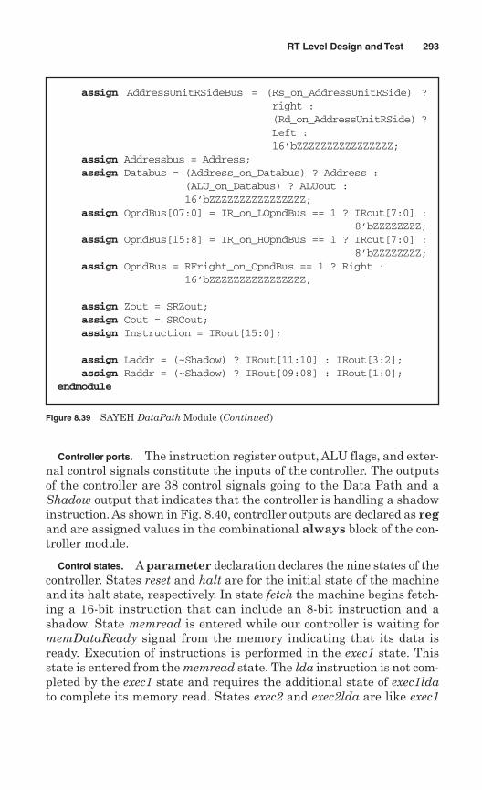
Controller ports. The instruction register output, ALU flags, and exter-nal control signals constitute the inputs of the controller. The outputsof the controller are 38 control signals going to the Data Path and aShadow output that indicates that the controller is handling a shadowinstruction. As shown in Fig. 8.40, controller outputs are declared as regand are assigned values in the combinational always block of the con-troller module.
Control states. A parameter declaration declares the nine states of thecontroller. States reset and halt are for the initial state of the machineand its halt state, respectively. In state fetch the machine begins fetch-ing a 16-bit instruction that can include an 8-bit instruction and ashadow. State memread is entered while our controller is waiting formemDataReady signal from the memory indicating that its data isready. Execution of instructions is performed in the exec1 state. Thisstate is entered from the memread state. The lda instruction is not com-pleted by the exec1 state and requires the additional state of exec1ldato complete its memory read. States exec2 and exec2lda are like exec1
RT Level Design and Test 293
Figure 8.39 SAYEH DataPath Module (Continued)
assign AddressUnitRSideBus = (Rs_on_AddressUnitRSide) ?right :(Rd_on_AddressUnitRSide) ?Left :16’bZZZZZZZZZZZZZZZZ;
assign Addressbus = Address;assign Databus = (Address_on_Databus) ? Address :
(ALU_on_Databus) ? ALUout :16’bZZZZZZZZZZZZZZZZ;
assign OpndBus[07:0] = IR_on_LOpndBus == 1 ? IRout[7:0] :8’bZZZZZZZZ;
assign OpndBus[15:8] = IR_on_HOpndBus == 1 ? IRout[7:0] : 8’bZZZZZZZZ;
assign OpndBus = RFright_on_OpndBus == 1 ? Right : 16’bZZZZZZZZZZZZZZZZ;
assign Zout = SRZout; assign Cout = SRCout;assign Instruction = IRout[15:0];
assign Laddr = (~Shadow) ? IRout[11:10] : IRout[3:2];assign Raddr = (~Shadow) ? IRout[09:08] : IRout[1:0];
endmodule
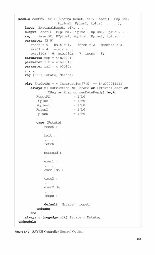
Figure 8.40 SAYEH Controller General Outline
module controller ( ExternalReset, clk, ResetPC, PCplusI,PCplus1, RplusI, Rplus0, . . . );
input ExternalReset, clk, . . .output ResetPC, PCplusI, PCplus1, RplusI, Rplus0, . . .reg ResetPC, PCplusI, PCplus1, RplusI, Rplus0, . . .parameter [3:0]
reset = 0, halt = 1, fetch = 2, memread = 3,exec1 = 4, exec2 = 5,exec1lda = 6, exec2lda = 7, incpc = 8;
parameter nop = 4’b0000;parameter hlt = 4’b0001;parameter szf = 4’b0010;. . .reg [3:0] Pstate, Nstate;
wire ShadowEn = ~(Instruction[7:0] == 8’b000011111)always @(Instruction or Pstate or ExternalReset or
Cflag or Zflag or memDataReady) beginResetPC = 1’b0;PCplusI = 1’b0;PCplus1 = 1’b0;RplusI = 1’b0;Rplus0 = 1’b0;. . .case (Pstate)
reset :. . .halt : . . .fetch : . . .memread :. . .exec1 : . . .exec1lda : . . .exec2 : . . .exec2lda : . . .incpc : . . .default: Nstate = reset;
endcaseend
always @ (negedge clk) Pstate = Nstate;endmodule
294
and exec1lda except that they handle the shadow part of an instruction.The execute state of most instructions (exec1 or exec2) increments the pro-gram counter while the instruction is being executed. However, certaininstructions that use the address bus for their execution cannot incrementPC while they are being executed. For these instructions, the incpc stateincrements the program counter.
Opcodes. Referring to Fig. 8.40, instruction opcodes are declared as4-bit parameters in the controller of SAYEH. These parameters areaccording to the processor’s instruction set of Table 8.1.
State declarations. As mentioned, the coding style of the controller isaccording to the Huffman style of coding discussed in Chap. 5. The nextstate and present states, required by this style of coding, are declaredin the controller of SAYEH as 4-bit registers, Nstate, and Pstate.
Shadow instructions. The ShadowEn signal that is internal to the con-troller is set when the hex code 0F (this code indicates that the right-most bits are not used) is not found in the right-most 8 bits of a 16-bitinstruction. If this wire is 1 and execution of an 8-bit instruction is com-plete, the controller branches to exec2 to execute the second half of theinstruction before the next fetching begins.
Combinational block. The combinational block of SAYEH controller hasan always block that has a main case statement with case choices forevery state of the machine. Transitions from one state to another andissuing control signals are performed in the case statement. At thebeginning of the always statement, all control signals are set to theirinactive values in order to avoid latches on these outputs.
Sequential block. The last part of the code outline of Fig. 8.40 is thesequential always block for clocking Pstate into Nstate. The controlstate register of SAYEH and all its data registers are falling edge trig-gered. Control signals issues by the controller remain active through thenext falling edge of the system clock.
Instruction execution. Figure 8.41 zooms on the combinational alwaysstatement of the controller module and shows the details of executionof mvr in the exec1 state of the controller. Signals issued for the exe-cution of this instruction are shown in this figure. This instructionreads a word from the right address of the Register File and writes itinto its left address. The right and left (source and destination)addresses are provided in the Data Path by connections made from IRto the Register File.
The RFright_on_OpndBus control signal is issued to read the sourceregister from RegisterFile onto OpndBus. Since this bus is the input of
RT Level Design and Test 295
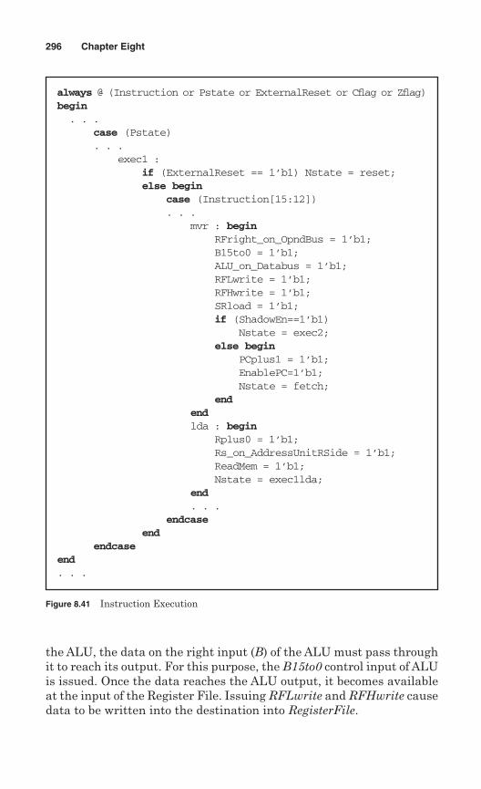
296 Chapter Eight
Figure 8.41 Instruction Execution
always @ (Instruction or Pstate or ExternalReset or Cflag or Zflag)begin. . .
case (Pstate). . .
exec1 : if (ExternalReset == 1’b1) Nstate = reset;else begin
case (Instruction[15:12]). . .
mvr : beginRFright_on_OpndBus = 1’b1;B15to0 = 1’b1;ALU_on_Databus = 1’b1;RFLwrite = 1’b1;RFHwrite = 1’b1;SRload = 1’b1;if (ShadowEn==1’b1)
Nstate = exec2;else begin
PCplus1 = 1’b1;EnablePC=1’b1;Nstate = fetch;
endendlda : begin
Rplus0 = 1’b1;Rs_on_AddressUnitRSide = 1’b1;ReadMem = 1’b1;Nstate = exec1lda;
end. . .
endcaseend
endcaseend. . .
the ALU, the data on the right input (B) of the ALU must pass throughit to reach its output. For this purpose, the B15to0 control input of ALUis issued. Once the data reaches the ALU output, it becomes availableat the input of the Register File. Issuing RFLwrite and RFHwrite causedata to be written into the destination into RegisterFile.
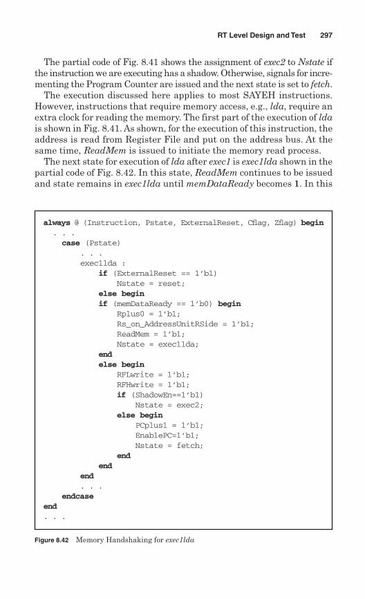
The partial code of Fig. 8.41 shows the assignment of exec2 to Nstate ifthe instruction we are executing has a shadow. Otherwise, signals for incre-menting the Program Counter are issued and the next state is set to fetch.
The execution discussed here applies to most SAYEH instructions.However, instructions that require memory access, e.g., lda, require anextra clock for reading the memory. The first part of the execution of ldais shown in Fig. 8.41. As shown, for the execution of this instruction, theaddress is read from Register File and put on the address bus. At thesame time, ReadMem is issued to initiate the memory read process.
The next state for execution of lda after exec1 is exec1lda shown in thepartial code of Fig. 8.42. In this state, ReadMem continues to be issuedand state remains in exec1lda until memDataReady becomes 1. In this
RT Level Design and Test 297
Figure 8.42 Memory Handshaking for exec1lda
always @ (Instruction, Pstate, ExternalReset, Cflag, Zflag) begin. . .case (Pstate)
. . .exec1lda :
if (ExternalReset == 1’b1)Nstate = reset;
else beginif (memDataReady == 1’b0) begin
Rplus0 = 1’b1;Rs_on_AddressUnitRSide = 1’b1;ReadMem = 1’b1;Nstate = exec1lda;
endelse begin
RFLwrite = 1’b1;RFHwrite = 1’b1;if (ShadowEn==1’b1)
Nstate = exec2;else begin
PCplus1 = 1’b1;EnablePC=1’b1;Nstate = fetch;
endend
end. . .
endcaseend. . .
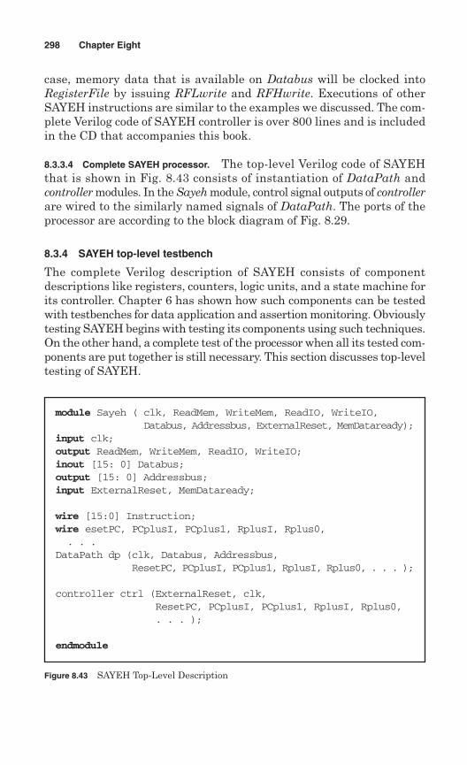
case, memory data that is available on Databus will be clocked intoRegisterFile by issuing RFLwrite and RFHwrite. Executions of otherSAYEH instructions are similar to the examples we discussed. The com-plete Verilog code of SAYEH controller is over 800 lines and is includedin the CD that accompanies this book.
8.3.3.4 Complete SAYEH processor. The top-level Verilog code of SAYEHthat is shown in Fig. 8.43 consists of instantiation of DataPath andcontroller modules. In the Sayeh module, control signal outputs of controllerare wired to the similarly named signals of DataPath. The ports of theprocessor are according to the block diagram of Fig. 8.29.
8.3.4 SAYEH top-level testbench
The complete Verilog description of SAYEH consists of componentdescriptions like registers, counters, logic units, and a state machine forits controller. Chapter 6 has shown how such components can be testedwith testbenches for data application and assertion monitoring. Obviouslytesting SAYEH begins with testing its components using such techniques.On the other hand, a complete test of the processor when all its tested com-ponents are put together is still necessary. This section discusses top-leveltesting of SAYEH.
298 Chapter Eight
Figure 8.43 SAYEH Top-Level Description
module Sayeh ( clk, ReadMem, WriteMem, ReadIO, WriteIO,Databus, Addressbus, ExternalReset, MemDataready);
input clk;output ReadMem, WriteMem, ReadIO, WriteIO;inout [15: 0] Databus;output [15: 0] Addressbus;input ExternalReset, MemDataready;
wire [15:0] Instruction;wire esetPC, PCplusI, PCplus1, RplusI, Rplus0,. . .
DataPath dp (clk, Databus, Addressbus, ResetPC, PCplusI, PCplus1, RplusI, Rplus0, . . . );
controller ctrl (ExternalReset, clk, ResetPC, PCplusI, PCplus1, RplusI, Rplus0,. . . );
endmodule
In a testbench, we instantiate SAYEH, and through a memory model,we apply instructions to the CPU and watch its response to these testinstructions. For developing such a top-level testbench that is easy forthe design engineer to work with, two issues must be considered: Testdata format and memory size handling.
Test data format must be at a high level so that the designer testingthe CPU can apply large volumes of instructions and data to the CPU.For this purpose, our testbench takes test data in the form of SAYEHinstructions and translates them to binary data for the processor to betested. This scheme was used for our simple AddingCPU and was dis-cussed in the previous section. SAYEH testbench has such a translationprogram that is, of course, much larger than that of AddingCPU.
The other issue that must be considered for a testbench for this designis memory size handling. Recall that our AddingCPU example did allits reading and writings directly into an external file representing itscomplete memory. Having the complete memory image in one file is notpractical for the relatively large size of SAYEH memory. Furthermore,moving the complete memory image of the processor being tested intoits testbench and declaring it as a two dimensional reg requires toomuch memory of the computer performing the simulation. In a largedesign, the actual memory of a design being tested may be larger thanthe computer it is being tested on.
In developing a testbench for SAYEH, we focus on the issue of memorysize handling discussed above. Instead of having all memory image inone file, or all of it declared as a reg, we take an in-between approach.We partition the memory of the circuit being tested (SAYEH CPU, in ourcase) into several pages, and use one file for each page. The file corre-sponding to a page is named according to the page number it represents.Then, the actual testbench declares a reg of the size of only one suchpage. This reg is regarded as a buffer. When the CPU model addressesa memory location, the testbench checks to see if that is available in thebuffer. If so, data from the buffer will be read or written into accordingto the CPU request. On the other hand, if a memory location is addressedthat is not in the buffer, the testbench writes the contents of the bufferinto its corresponding memory file, and loads the page that has theaddressed location into the buffer.
Figure 8.44 shows the overall structure of our testbench. The sec-tions that follow discuss the details of the Verilog code of this testbench.The complete code of this testbench is included in the CD that accom-panies this book.
8.3.4.1 Testbench Verilog outline. The outline of the Verilog code ofSAYEH testbench is shown in Fig. 8.45. This code corresponds to the
RT Level Design and Test 299
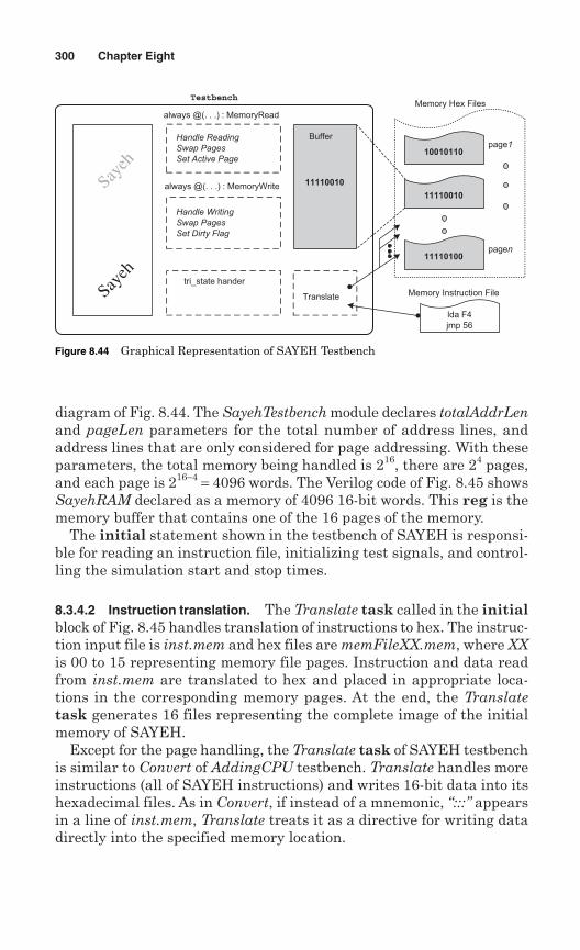
diagram of Fig. 8.44. The SayehTestbench module declares totalAddrLenand pageLen parameters for the total number of address lines, andaddress lines that are only considered for page addressing. With theseparameters, the total memory being handled is 216, there are 24 pages,and each page is 216−4 = 4096 words. The Verilog code of Fig. 8.45 showsSayehRAM declared as a memory of 4096 16-bit words. This reg is thememory buffer that contains one of the 16 pages of the memory.
The initial statement shown in the testbench of SAYEH is responsi-ble for reading an instruction file, initializing test signals, and control-ling the simulation start and stop times.
8.3.4.2 Instruction translation. The Translate task called in the initialblock of Fig. 8.45 handles translation of instructions to hex. The instruc-tion input file is inst.mem and hex files are memFileXX.mem, where XXis 00 to 15 representing memory file pages. Instruction and data readfrom inst.mem are translated to hex and placed in appropriate loca-tions in the corresponding memory pages. At the end, the Translatetask generates 16 files representing the complete image of the initialmemory of SAYEH.
Except for the page handling, the Translate task of SAYEH testbenchis similar to Convert of AddingCPU testbench. Translate handles moreinstructions (all of SAYEH instructions) and writes 16-bit data into itshexadecimal files. As in Convert, if instead of a mnemonic, “:::” appearsin a line of inst.mem, Translate treats it as a directive for writing datadirectly into the specified memory location.
300 Chapter Eight
11110010
Memory Hex Files
Memory Instruction File
Testbench
Handle Reading
Swap Pages
Set Active Page
tri_state hander
page1
pagen
Buffer
Translate
Handle Writing
Swap Pages
Set Dirty Flag
always @(. . .) : MemoryRead
always @(. . .) : MemoryWrite
10010110
11110100
lda F4jmp 56
11110010
Sayeh
Sayeh
Figure 8.44 Graphical Representation of SAYEH Testbench
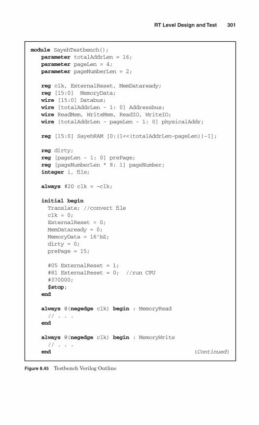
RT Level Design and Test 301
Figure 8.45 Testbench Verilog Outline
module SayehTestbench();parameter totalAddrLen = 16;parameter pageLen = 4;parameter pageNumberLen = 2;
reg clk, ExternalReset, MemDataready;reg [15:0] MemoryData;wire [15:0] Databus;wire [totalAddrLen - 1: 0] Addressbus;wire ReadMem, WriteMem, ReadIO, WriteIO;wire [totalAddrLen - pageLen - 1: 0] physicalAddr;
reg [15:0] SayehRAM [0:(1<<(totalAddrLen-pageLen))-1];
reg dirty;reg [pageLen - 1: 0] prePage;reg [pageNumberLen * 8: 1] pageNumber;integer i, file;
always #20 clk = ~clk;
initial beginTranslate; //convert fileclk = 0;ExternalReset = 0;MemDataready = 0;MemoryData = 16’bZ;dirty = 0;prePage = 15;
#05 ExternalReset = 1;#81 ExternalReset = 0; //run CPU#370000;$stop;
end
always @(negedge clk) begin : MemoryRead// . . .
end
always @(negedge clk) begin : MemoryWrite // . . .
end (Continued)
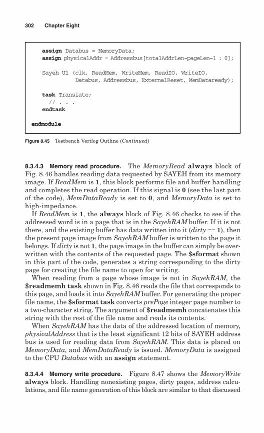
8.3.4.3 Memory read procedure. The MemoryRead always block ofFig. 8.46 handles reading data requested by SAYEH from its memoryimage. If ReadMem is 1, this block performs file and buffer handlingand completes the read operation. If this signal is 0 (see the last partof the code), MemDataReady is set to 0, and MemoryData is set tohigh-impedance.
If ReadMem is 1, the always block of Fig. 8.46 checks to see if theaddressed word is in a page that is in the SayehRAM buffer. If it is notthere, and the existing buffer has data written into it (dirty == 1), thenthe present page image from SayehRAM buffer is written to the page itbelongs. If dirty is not 1, the page image in the buffer can simply be over-written with the contents of the requested page. The $sformat shownin this part of the code, generates a string corresponding to the dirtypage for creating the file name to open for writing.
When reading from a page whose image is not in SayehRAM, the$readmemh task shown in Fig. 8.46 reads the file that corresponds tothis page, and loads it into SayehRAM buffer. For generating the properfile name, the $sformat task converts prePage integer page number toa two-character string. The argument of $readmemh concatenates thisstring with the rest of the file name and reads its contents.
When SayehRAM has the data of the addressed location of memory,physicalAddress that is the least significant 12 bits of SAYEH addressbus is used for reading data from SayehRAM. This data is placed onMemoryData, and MemDataReady is issued. MemoryData is assignedto the CPU Databus with an assign statement.
8.3.4.4 Memory write procedure. Figure 8.47 shows the MemoryWritealways block. Handling nonexisting pages, dirty pages, address calcu-lations, and file name generation of this block are similar to that discussed
302 Chapter Eight
Figure 8.45 Testbench Verilog Outline (Continued)
assign Databus = MemoryData;assign physicalAddr = Addressbus[totalAddrLen-pageLen–1 : 0];
Sayeh U1 (clk, ReadMem, WriteMem, ReadIO, WriteIO,Databus, Addressbus, ExternalReset, MemDataready);
task Translate;// . . .
endtask
endmodule
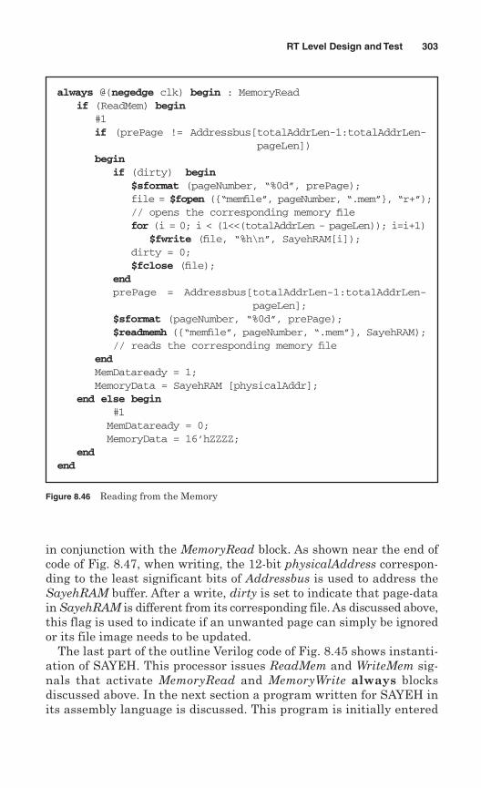
in conjunction with the MemoryRead block. As shown near the end ofcode of Fig. 8.47, when writing, the 12-bit physicalAddress correspon-ding to the least significant bits of Addressbus is used to address theSayehRAM buffer. After a write, dirty is set to indicate that page-datain SayehRAM is different from its corresponding file. As discussed above,this flag is used to indicate if an unwanted page can simply be ignoredor its file image needs to be updated.
The last part of the outline Verilog code of Fig. 8.45 shows instanti-ation of SAYEH. This processor issues ReadMem and WriteMem sig-nals that activate MemoryRead and MemoryWrite always blocksdiscussed above. In the next section a program written for SAYEH inits assembly language is discussed. This program is initially entered
RT Level Design and Test 303
Figure 8.46 Reading from the Memory
always @(negedge clk) begin : MemoryReadif (ReadMem) begin
#1if (prePage != Addressbus[totalAddrLen-1:totalAddrLen-
pageLen])begin
if (dirty) begin$sformat (pageNumber, “%0d”, prePage);file = $fopen ({“memfile”, pageNumber, “.mem”}, “r+”);// opens the corresponding memory filefor (i = 0; i < (1<<(totalAddrLen - pageLen)); i=i+1)
$fwrite (file, “%h\n”, SayehRAM[i]);dirty = 0;$fclose (file);
endprePage = Addressbus[totalAddrLen-1:totalAddrLen-
pageLen];$sformat (pageNumber, “%0d”, prePage);$readmemh ({“memfile”, pageNumber, “.mem”}, SayehRAM);// reads the corresponding memory file
endMemDataready = 1;MemoryData = SayehRAM [physicalAddr];
end else begin#1MemDataready = 0;MemoryData = 16’hZZZZ;
endend
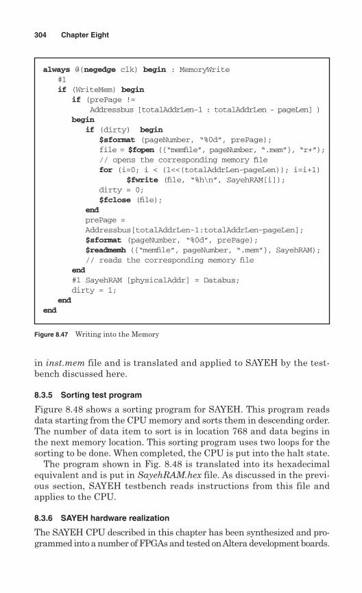
in inst.mem file and is translated and applied to SAYEH by the test-bench discussed here.
8.3.5 Sorting test program
Figure 8.48 shows a sorting program for SAYEH. This program readsdata starting from the CPU memory and sorts them in descending order.The number of data item to sort is in location 768 and data begins inthe next memory location. This sorting program uses two loops for thesorting to be done. When completed, the CPU is put into the halt state.
The program shown in Fig. 8.48 is translated into its hexadecimalequivalent and is put in SayehRAM.hex file. As discussed in the previ-ous section, SAYEH testbench reads instructions from this file andapplies to the CPU.
8.3.6 SAYEH hardware realization
The SAYEH CPU described in this chapter has been synthesized and pro-grammed into a number of FPGAs and tested on Altera development boards.
304 Chapter Eight
Figure 8.47 Writing into the Memory
always @(negedge clk) begin : MemoryWrite #1if (WriteMem) begin
if (prePage !=Addressbus [totalAddrLen-1 : totalAddrLen - pageLen] )
beginif (dirty) begin
$sformat (pageNumber, “%0d”, prePage);file = $fopen ({“memfile”, pageNumber, “.mem”}, “r+”);// opens the corresponding memory filefor (i=0; i < (1<<(totalAddrLen-pageLen)); i=i+1)
$fwrite (file, “%h\n”, SayehRAM[i]);dirty = 0;$fclose (file);
endprePage =Addressbus[totalAddrLen-1:totalAddrLen-pageLen];$sformat (pageNumber, “%0d”, prePage);$readmemh ({“memfile”, pageNumber, “.mem”}, SayehRAM);// reads the corresponding memory file
end#1 SayehRAM [physicalAddr] = Databus;dirty = 1;
endend
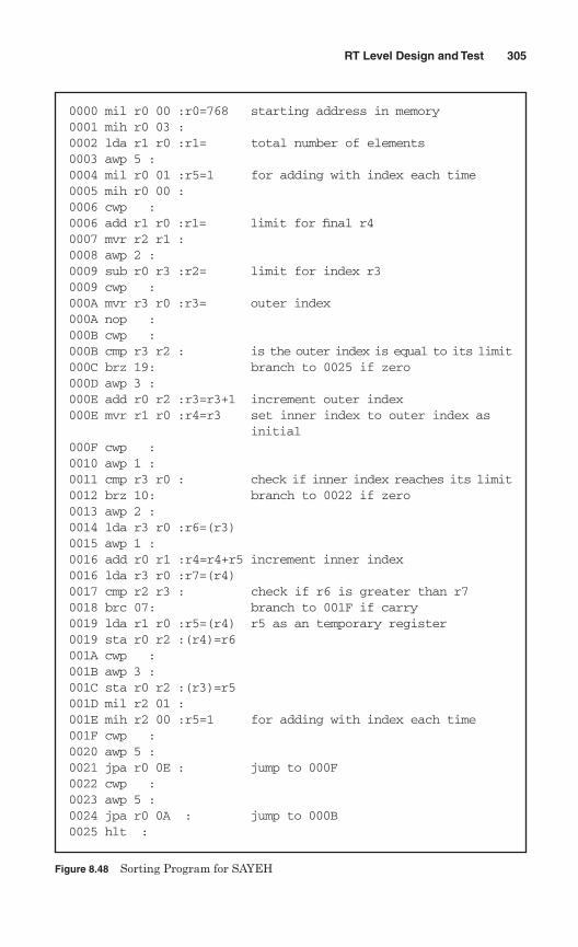
RT Level Design and Test 305
Figure 8.48 Sorting Program for SAYEH
0000 mil r0 00 :r0=768 starting address in memory0001 mih r0 03 :0002 lda r1 r0 :r1= total number of elements0003 awp 5 :0004 mil r0 01 :r5=1 for adding with index each time0005 mih r0 00 :0006 cwp :0006 add r1 r0 :r1= limit for final r40007 mvr r2 r1 :0008 awp 2 :0009 sub r0 r3 :r2= limit for index r30009 cwp :000A mvr r3 r0 :r3= outer index000A nop :000B cwp :000B cmp r3 r2 : is the outer index is equal to its limit000C brz 19: branch to 0025 if zero000D awp 3 :000E add r0 r2 :r3=r3+1 increment outer index000E mvr r1 r0 :r4=r3 set inner index to outer index as
initial000F cwp :0010 awp 1 :0011 cmp r3 r0 : check if inner index reaches its limit0012 brz 10: branch to 0022 if zero0013 awp 2 : 0014 lda r3 r0 :r6=(r3)0015 awp 1 :0016 add r0 r1 :r4=r4+r5 increment inner index0016 lda r3 r0 :r7=(r4)0017 cmp r2 r3 : check if r6 is greater than r70018 brc 07: branch to 001F if carry0019 lda r1 r0 :r5=(r4) r5 as an temporary register0019 sta r0 r2 :(r4)=r6001A cwp :001B awp 3 :001C sta r0 r2 :(r3)=r5001D mil r2 01 :001E mih r2 00 :r5=1 for adding with index each time001F cwp :0020 awp 5 :0021 jpa r0 0E : jump to 000F0022 cwp :0023 awp 5 :0024 jpa r0 0A : jump to 000B0025 hlt :
One implementation has been on Altera’s FLEX device of an AlteraUP2. We used a RAM from Altera’s megafunctions and configured it asa memory of 1024 16-bit words. The number of logic elements used bythis CPU was 1,125, which is 30% of the available LEs. Memory bitsused was 16,384, which is 44% of the available memory bits. This usageindicates that we can form a complete system with a keyboard and VGAoutput on a FLEX 10K of UP2.
8.4 Summary
This chapter showed design, testing, and implementation of several RTlevel designs of a complete CPU. This design put all that we have cov-ered in this book into one package. The design is complete and typicalof any large system with a complex controller and data path. Use of thesynthesizable subset of Verilog to develop for development of a designfor FPGA programming was shown. On the other hand, utilization ofbehavioral constructs of Verilog was demonstrated in developing a test-bench for our processor.
Problems
8.1 Design a 2’s complement multiplier using Booth’s algorithm. Your designshould consist of two units, a controller and a datapath. The multiplier has an8-bit A and B inputs and a 16-bit result.
8.2 Design a multiplier that performs its 4 × 4 multiplications by a memorylookup. Your design should consist of a controller and a datapath. The multiplierhas 8-bit A and B inputs and a 16-bit result. The addresses in the memory canat most be 8-bit.
8.3 In this problem you are to design a Single Cycle processor. The processorhas a 16 bit external data bus, and a 12 bit address bus for memory or read andwrite. The processor has a 16 bit register (acc), which is used as an operand inarithmetic instructions and as an accumulator for holding data read from memoryin load instructions. The processor can address 4048 16-bit words of the memory.Memory read and write operations are synchronous with the system clock andthey are completed in one cycle. In reading from the memory, the address buscontaining the address of the desired memory cell and the read signal should beissued to the data memory block. In writing into memory, the address and thewrite signal should be issued. The machine has 16-bit instructions consisting ofa 4-bit opcode and a 12-bit address. The processor has three types of instructions:arithmetic and logical instructions (ADD, CPL, AND, INC), data-transferinstructions (STA, LDA), and control-flow instructions (JNZ, JMP). JNZ isjump and acc is zero. Table shown below, shows processor instructions.
306 Chapter Eight
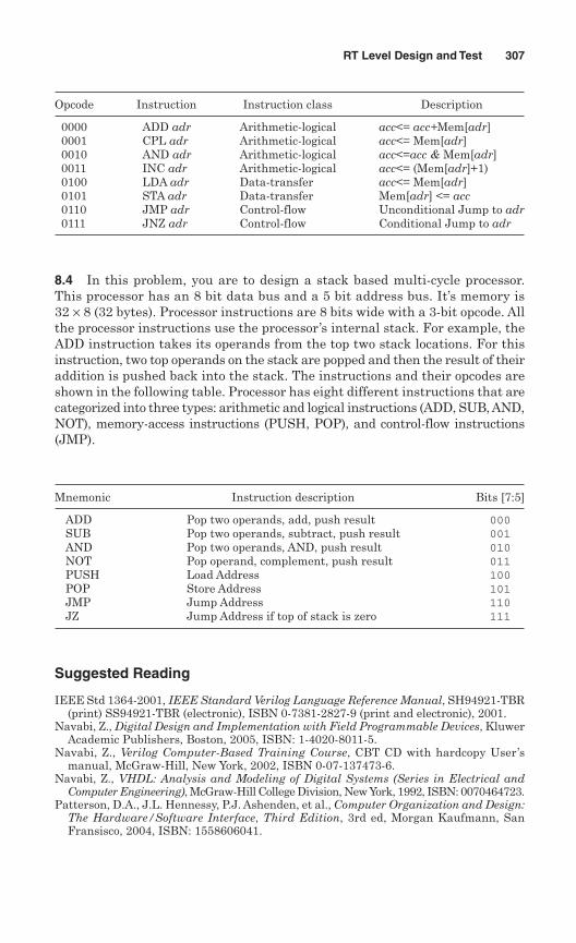
8.4 In this problem, you are to design a stack based multi-cycle processor.This processor has an 8 bit data bus and a 5 bit address bus. It’s memory is32 × 8 (32 bytes). Processor instructions are 8 bits wide with a 3-bit opcode. Allthe processor instructions use the processor’s internal stack. For example, theADD instruction takes its operands from the top two stack locations. For thisinstruction, two top operands on the stack are popped and then the result of theiraddition is pushed back into the stack. The instructions and their opcodes areshown in the following table. Processor has eight different instructions that arecategorized into three types: arithmetic and logical instructions (ADD, SUB, AND,NOT), memory-access instructions (PUSH, POP), and control-flow instructions(JMP).
RT Level Design and Test 307
Opcode Instruction Instruction class Description
0000 ADD adr Arithmetic-logical acc<= acc+Mem[adr]0001 CPL adr Arithmetic-logical acc<= Mem[adr]0010 AND adr Arithmetic-logical acc<=acc & Mem[adr]0011 INC adr Arithmetic-logical acc<= (Mem[adr]+1)0100 LDA adr Data-transfer acc<= Mem[adr]0101 STA adr Data-transfer Mem[adr] <= acc0110 JMP adr Control-flow Unconditional Jump to adr0111 JNZ adr Control-flow Conditional Jump to adr
Mnemonic Instruction description Bits [7:5]
ADD Pop two operands, add, push result 000SUB Pop two operands, subtract, push result 001AND Pop two operands, AND, push result 010NOT Pop operand, complement, push result 011PUSH Load Address 100POP Store Address 101JMP Jump Address 110JZ Jump Address if top of stack is zero 111
Suggested Reading
IEEE Std 1364-2001, IEEE Standard Verilog Language Reference Manual, SH94921-TBR(print) SS94921-TBR (electronic), ISBN 0-7381-2827-9 (print and electronic), 2001.
Navabi, Z., Digital Design and Implementation with Field Programmable Devices, KluwerAcademic Publishers, Boston, 2005, ISBN: 1-4020-8011-5.
Navabi, Z., Verilog Computer-Based Training Course, CBT CD with hardcopy User’smanual, McGraw-Hill, New York, 2002, ISBN 0-07-137473-6.
Navabi, Z., VHDL: Analysis and Modeling of Digital Systems (Series in Electrical andComputer Engineering), McGraw-Hill College Division, New York, 1992, ISBN: 0070464723.
Patterson, D.A., J.L. Hennessy, P.J. Ashenden, et al., Computer Organization and Design:The Hardware/Software Interface, Third Edition, 3rd ed, Morgan Kaufmann, SanFransisco, 2004, ISBN: 1558606041.

This page intentionally left blank

Appendix
AList of Keywords
Verilog keywords are predefined identifiers used in the Verilog languageconstructs.
309
always
and
assign
automatic
begin
buf
bufif0
bufif1
case
casex
casez
cell
cmos
config
deassign
default
defparam
design
disable
edge
else
end
endcase
endconfig
endfunction
endgenerate
endmodule
endprimitive
endspecify
endtable
endtask
event
for
force
forever
fork
function
generate
genvar
highz0
highz1
if
ifnone
incdir
include
initial
inout
input
instance
integer
join
large
liblist
library
localparam
macromodule
medium
module
nand
negedge
nmos
nor
noshowcancelled
not
notif0
notif1
Copyright © 2006 by The McGraw-Hill Publishing Companies, Inc. Click here for terms of use.
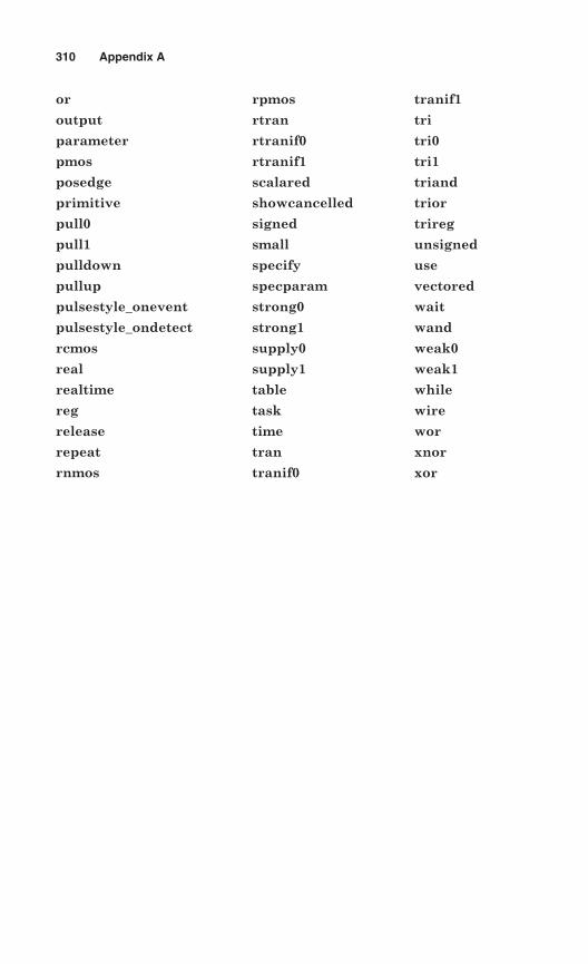
310 Appendix A
or
output
parameter
pmos
posedge
primitive
pull0
pull1
pulldown
pullup
pulsestyle_onevent
pulsestyle_ondetect
rcmos
real
realtime
reg
release
repeat
rnmos
rpmos
rtran
rtranif0
rtranif1
scalared
showcancelled
signed
small
specify
specparam
strong0
strong1
supply0
supply1
table
task
time
tran
tranif0
tranif1
tri
tri0
tri1
triand
trior
trireg
unsigned
use
vectored
wait
wand
weak0
weak1
while
wire
wor
xnor
xor
Appendix
BFrequently Used
System Tasks and Functions
This appendix includes a list of frequently used Verilog system tasksand functions for reference. For each such utility a brief description isprovided. Examples for these and other system tasks are included inthe chapters. The details of system tasks not discussed here and cor-responding examples can be found in Chap. 7.
B.1 Display Tasks
$display The $displayb task displays its arguments in the order that theyappear. Display will be done to the standard output device. When invoked, italways inserts a newline character at the end of its output string. Strings to bedisplayed as well as format specifications must appear in double quotes as anargument of this task. Task invocation,
$display ( “Counter value is: %d”, cnt);
prints value of cnt variable in decimal format. Decimal format is assumed if noformat specification exists for a variable or expression.
$displayb The $displayb task displays its arguments in the order that theyappear. Display will be done to the standard output device. When invoked, italways inserts a newline character at the end of its output string. Strings to bedisplayed as well as format specifications must appear in double quotes as anargument of this task. Task invocation,
$displayb ( “Counter value is: %o”, cnt);
prints value of cnt variable in octal format. Binary format is assumed if noformat specification exists for a variable or expression.
311
Copyright © 2006 by The McGraw-Hill Publishing Companies, Inc. Click here for terms of use.
$displayh The $displayh task displays its arguments in the order that theyappear. Display will be done to the standard output device. When invoked, italways inserts a newline character at the end of its output string. Strings to bedisplayed as well as format specifications must appear in double quotes as anargument of this task. Task invocation,
$displayh ( “Counter value is: %b”, cnt);
prints value of cnt variable in binary format. Hexadecimal format is assumedif no format specification exists for a variable or expression.
$displayo The $displayo task displays its arguments in the order that theyappear. Display will be done to the standard output device. When invoked, italways inserts a newline character at the end of its output string. Strings to bedisplayed, as well as, format specifications must appear in double quotes as anargument of this task. Task invocation,
$displayo ( “Counter value is: %h”, cnt);
prints value of cnt variable in hexadecimal format. Octal format is assumed ifno format specification exists for a variable or expression.
$monitoron Turns on the monitor flag used by various forms of the $monitorsystem task. Monitoring will be enabled.
$monitoroff Turns off the monitor flag used by various forms of the $monitorsystem task. Monitoring will be disabled.
$monitor While monitor flag is on, when a variable or an expression onthe argument list changes value, the entire argument list is displayed as in the$display system task.
$monitorb While monitor flag is on, when a variable or an expression onthe argument list changes value, the entire argument list is displayed as in the$displayb system task.
$monitorh While monitor flag is on, when a variable or an expression onthe argument list changes value, the entire argument list is displayed as in the$displayh system task.
$monitoro While monitor flag is on, when a variable or an expression onthe argument list changes value, the entire argument list is displayed as in the$displayo system task.
$strobe Using the same format as in $display, the $strobe system task dis-plays its arguments in a simulation cycle after all events have expired.
$strobeb Using the same format as in $displayb, the $strobeb system taskdisplays its arguments in a simulation cycle after all events have expired.
$strobeh Using the same format as in $displayh, the $strobeh system taskdisplays its arguments in a simulation cycle after all events have expired.
312 Appendix B
$strobeo Using the same format as in $displayo, the $strobeo system taskdisplays its arguments in a simulation cycle after all events have expired.
$write The $write task displays its arguments in the order that they appearusing the same format as in $display. Unlike the $display task a newlinecharacter is not added to the end of its output, and consecutive outputs continueon the same line.
$writeb The $writeb task displays its arguments in the order that theyappear using the same format as in $displayb. Unlike the $displayb task anewline character is not added to the end of its output, and consecutive outputscontinue on the same line.
$writeh The $writeh task displays its arguments in the order that theyappear using the same format as in $displayh. Unlike the $displayh task anewline character is not added to the end of its output, and consecutive outputscontinue on the same line.
$writeo The $writeo task displays its arguments in the order that theyappear using the same format as in $displayo. Unlike the $displayo task anewline character is not added to the end of its output, and consecutive outputscontinue on the same line.
B.2 File I/O Tasks
$fopen The $fopen system function returns a file descriptor for the physicalfile specified as a string in the function argument. The following example makesdesc a descriptor for the physical file dataset.dat.
integer desc = $fopen (“dataset.dat”);
$fclose The $fclose task closes an open file. The only argument of this taskis a file descriptor for an open file.
$fdisplay The $fdisplay task outputs its arguments in the order that theyappear. Writing will be done to a file specified by its descriptor. The file descrip-tor must appear first in the task argument list. This task uses the same for-matting as in the $display task. Task invocation,
$fdisplay (desc, “Counter value is: %d”, cnt);
prints value of cnt variable in decimal format. Decimal format is assumed if noformat specification exists for a variable or expression.
$fdisplayb The $fdisplay task outputs its arguments in the order that theyappear. Writing will be done to a file specified by its descriptor. The file descrip-tor must appear first in the task argument list. This task uses the same for-matting as in the $displayb task. Task invocation,
$fdisplayb (desc, “Counter value is: %d”, cnt);
Frequently Used System Tasks and Functions 313
prints value of cnt variable in decimal format. Binary format is assumed if noformat specification exists for a variable or expression.
$fdisplayh The $fdisplayh task outputs its arguments in the order thatthey appear. Writing will be done to a file specified by its descriptor. The filedescriptor must appear first in the task argument list. This task uses the sameformatting as in the $displayh task. Task invocation,
$fdisplayh (desc, “Counter value is: %d”, cnt);
prints value of cnt variable in decimal format. Hexadecimal format is assumedif no format specification exists for a variable or expression.
$fdisplayo The $fdisplayo task outputs its arguments in the order that theyappear. Writing will be done to a file specified by its descriptor. The file descrip-tor must appear first in the task argument list. This task uses the same for-matting as in the $displayo task. Task invocation,
$fdisplayo (desc, “Counter value is: %d”, cnt);
prints value of cnt variable in decimal format. Octal format is assumed if noformat specification exists for a variable or expression.
$fmonitor While monitor flag is on, when a variable or an expression on theargument list changes value, the entire argument list is written into a file. Thefile is specified by its descriptor which is the first argument in the task argu-ment list. This task uses the same formatting as in the $display task.
$fmonitorb While monitor flag is on, when a variable or an expression on theargument list changes value, the entire argument list is written into a file. Thefile is specified by its descriptor which is the first argument in the task argu-ment list. This task uses the same formatting as in the $displayb task.
$fmonitorh While monitor flag is on, when a variable or an expression on theargument list changes value, the entire argument list is written into a file. Thefile is specified by its descriptor which is the first argument in the task argu-ment list. This task uses the same formatting as in the $displayh task.
$fmonitoro While monitor flag is on, when a variable or an expression on theargument list changes value, the entire argument list is written into a file. Thefile is specified by its descriptor which is the first argument in the task argu-ment list. This task uses the same formatting as in the $displayo task.
$fstrobe Using the same format as in $display, the $fstrobe system taskwrites its arguments into a file specified by its descriptor as the first argumentof the task. Writing will be done in a simulation cycle after all events haveexpired.
$fstrobeb Using the same format as in $displayb, the $fstrobeb system taskwrites its arguments into a file specified by its descriptor as the first argumentof the task. Writing will be done in a simulation cycle after all events have expired.
314 Appendix B
$fstrobeh Using the same format as in $displayh, the $fstrobeh system taskwrites its arguments into a file specified by its descriptor as the first argumentof the task. Writing will be done in a simulation cycle after all events haveexpired.
$fstrobeo Using the same format as in $displayo, the $fstrobeo systemtask writes its arguments into a file specified by its descriptor as the first argu-ment of the task. Writing will be done in a simulation cycle after all events haveexpired.
$fwrite The $fwrite task is similar to the $fdisplay task except that it doesnot insert a newline character at the end of its output string. Descriptor for thefile into which writing is done appears first in the argument list of this task.
$fwriteb The $fwriteb task is similar to the $fdisplayb task except that itdoes not insert a newline character at the end of its output string. Descriptor forthe file into which writing is done appears first in the argument list of this task.
$fwriteh The $fwriteh task is similar to the $fdisplayh task except that itdoes not insert a newline character at the end of its output string. Descriptor forthe file into which writing is done appears first in the argument list of this task.
$fwriteo The $fwriteo task is similar to the $fdisplayo task except that itdoes not insert a newline character at the end of its output string. Descriptor forthe file into which writing is done appears first in the argument list of this task.
$readmemb A physical file name and a memory name are required argumentsof the $readmemb task. When invoked, this task reads binary data from filespecified in its argument and loads this data into the memory specified as itssecond parameter. Optionally, invocation of this task may contain range ofmemory words to fill.
If mem is declared as
reg [15:0] mem [0:511],
then, invocation shown below reads 16 bit words in binary from memdata.datfile and loads this data into memory locations 12 to 412.
$readmemb(“memdata.dat”, mem, 12, 412);
$readmemh A physical file name and a memory name are required argumentsof the #readmemh task. When invoked, this task reads hexadecimal data fromfile specified in its argument and loads this data into the memory specified asits second parameter. Optionally, invocation of this task may contain range ofmemory words to fill.
If mem is declared as
reg [15:0] mem [0:511],
Frequently Used System Tasks and Functions 315
then, invocation shown below reads 16 bit words in hexadecimal from memdata.datfile and loads this data into memory locations 12 to 412.
$readmemh(“memdata.dat”, mem, 12, 412);
$swrite The $swrite string output system task is similar to $fwrite butinstead of writing to a file it writes its arguments into a register. This task canbe used to convert data to string.
$sformat The $sformat task is another string output system task. This taskis similar to $swrite with one major difference; it always interprets its argu-ments as a format string.
$fgetc The $fgetc reads a byte (character) from a specified file, i.e., $fgetc(fd), reads from fd. The specified file must be opened with either r or r+ typevalues to make them available for reading.
$ungetc The $ungetc inserts a character into the buffer of a specified file.The character shall be returned by the next $fgetc call of the specified file. Thefile itself remains unchanged.
$fgets It reads characters from a specified file into a string register untileither the register is filled or a newline character is read from the file. An exam-ple usage is:
$fgets (string_name, file_descriptor);
$fscanf It reads data from a specified file into a register. It reads charactersand interprets them according to the format specified by it arguments.
$sscanf The $sscanf is similar to the $fscanf. The difference is that $sscanfreads from a string register.
$fread It reads binary data from a specified file and writes into a memory. Theaddress of the first data to be written and the number of them can be specifiedin this task.
$ftell The $ftell returns the offset from the beginning of a specified file. Thistask is useful for file positioning.
$fseek The $fseek task sets the position of the next input or output opera-tion on a specified file. The positioning can be specified by offset bytes from begin-ning of the file or current position, or from the end of the file. General formatof use of $fseek is shown below. The value of operation (0, 1, or 2) determinesif position is set to offset, offset plus current location, or EOF plus offset.
Code = $fseek (fd, offset, operation);
$rewind The $rewind task sets the position of a specified file to the begin-ning of the file.
316 Appendix B
$fflush The $fflush task writes any buffered output to a specified file. If $fflushis invoked with no arguments, it writes any buffered output to all open files.
$ferror It creates a string description of the type of the error encountered bythe most recent file I/O operation and writes it into a specified register.
B.3 Timescale Tasks
$printtimescale The $printtimescale task prints time unit and time preci-sion specified by ̀ timescale directive. If used without an argument this task con-siders `timescale of the module within which it is invoked. If used with anargument, the argument must be the hierarchical name of the module considered.
$timeformat The $timeformat task specifies how %t format specificationreports time information for various forms of display tasks. Arguments of thistask are unit number, precision number, suffix string, and field width. Unitnumber is an integer between 0 and 15 specifying time units 1s to 1fs respec-tively. Precision number argument specifies number of fractional digits of timereported. Suffix string argument is a string for textual representation of timeunit. The last argument specifies the width of time information output string.
B.3.1 Simulation control tasks
$finish When encountered in a procedural flow the $finish system task ter-minates and exits simulation. An integer between 0 and 2 passed to this taskas an argument specifies the type of message printed when task is invoked.
$stop The $stop system task suspends simulation when invoked. An integerbetween 0 and 2 passed to this task as an argument specifies the type of mes-sage printed when task is invoked.
B.4 Timing Check Tasks
$hold The $hold system task reports a violation when a reference eventoccurs too close to a data event. A time limit specifying hold time is the allowedtime distance between the reference and data events. The first argument spec-ifies the reference event such as the clock edge. The second argument specifiesthe data signal. The third argument specifies the hold time.
$hold (posedge clk, data, holdtime);
$period Time distance between consecutive events of the same kind (positiveor negative) is monitored by the $period task. The first argument is the refer-ence event and the second event is the time specifying the period.
$setup The $setup system task reports a violation when a data event occurstoo close to a reference event. A time limit, which is the setup time, specifies
Frequently Used System Tasks and Functions 317
allowed time distance between the data and reference events. The first argu-ment specifies the name of data signal. The second argument specifies the ref-erence event such as the clock edge. The third argument is the setup time. Anexample is:
$setup (data, posedge clk, setuptime);
$skew The $skew system task reports a violation when a reference event anda data event are too far a part in time. As in the $hold task, the reference eventis the first argument, the data event is the second argument and the skew timeis the third argument of this task.
$nochange The $nochange task reports a violation if during a level speci-fied by transition on reference event of its first argument, its second argumentchanges value. Offset time values specified by third and fourth argumentsexpand or shrink the time within which data events are monitored. The followingstatement report a violation if go changes while start is 0.
$nochange (negedge start, go, 0, 0);
$recovery The $recovery task is similar to the $setup task except that the$recovery task reports a violation if the data event and reference event occurat the same simulation time.
$setuphold The $setuphold task is invoked with arguments specifying a ref-erence event, a data event, setup time, and hold time in this order. This taskperforms both $setup and $hold tasks.
$width The $width system task reports a violation when a reference event,specified by its first argument, occurs too close to an opposite event on thisargument. The second argument of this task is the allowed pulse width.
318 Appendix B
Appendix
CCompiler Directives
This appendix briefly describes Verilog HDL compiler directives. Useand examples of such a language utility where described in Chaps. 7and 9.
`celldefine Bracketing modules between `celldefine and`endcelldefine `endcelldefine tags the modules as cells.
`default_nettype The `default_nettype directive sets the type ofimplicit nets. The default is wire.
`define The `define directive aliases an expression with`undef a name. The `undef directive turns of aliases set
by `define.
`ifdef Directives ̀ ifdef, ̀ else, and ̀ endif are if-then-else `else type bracketing for optional compilation of a`endif Verilog code.`include The ̀ include directive inserts text from an external
file.
`unconnected_drive The ̀ unconnected_drive and ̀ nounconnected_`nounconnected_drive drive directives bracket a portion of code for which
unconnected input ports will be treated pulled upor pulled down instead of normal default.
`resetall The ̀ resetall directive resets all directives to theirdefault values.
`timescale For setting time scale and time precision,`timescale is used.
319
Copyright © 2006 by The McGraw-Hill Publishing Companies, Inc. Click here for terms of use.

This page intentionally left blank
Appendix
DVerilog Formal
Syntax Definition
The formal syntax of Verilog HDL is described using Backus-Naur Form(BNF).
D.1 Source text
D.1.1 Library Source Text
library_text ::= { library_descriptions }library_descriptions ::=
library_declaration|include_statement|config_declaration
library_declaration ::=library library_identifier file_path_spec [ { , file_path_spec } ][ -incdir file_path_spec [ { , file_path_spec } ] ;
file_path_spec ::= file_pathinclude_statement ::= include <file_path_spec> ;
D.1.2 Configuration Source Text
config_declaration ::=config config_identifier ;design_statement{config_rule_statement}endconfig
design_statement ::= design { [library_identifier.]cell_identifier } ;config_rule_statement ::=
321
Copyright © 2006 by The McGraw-Hill Publishing Companies, Inc. Click here for terms of use.
default_clause liblist_clause|inst_clause liblist_clause|inst_clause use_clause|cell_clause liblist_clause|cell_clauseuse_clause
default_clause ::= defaultinst_clause ::= instance inst_nameinst_name ::= topmodule_identifier{.instance_identifier}cell_clause ::= cell [ library_identifier.]cell_identifierliblist_clause ::= liblist [{library_identifier}]use_clause ::= use [library_identifier.]cell_identifier[:config]
D.1.3 Module and Primitive Source Text
source_text ::= { description }description ::=
module_declaration|udp_declaration
module_declaration ::={ attribute_instance } module_keyword module_identifier [ module_
param eter_port_list ][ list_of_ports ] ; { module_item }endmodule
|{ attribute_instance } module_keyword module_identifier [ module_parameter_port_list ]
[ list_of_port_declarations ] ; { non_port_module_item }endmodule
module_keyword ::= module |macromodule
D.1.4 Module Parameters and Ports
module_parameter_port_list ::= # ( parameter_declaration { , parameter_declaration } )list_of_ports ::= ( port { , port } )list_of_port_declarations ::=
( port_declaration { , port_declaration } )|( )
port ::=[ port_expression ]
|. port_identifier ( [ port_expression ] )port_expression ::=
port_reference|{ port_reference { , port_reference } }
port_reference ::=port_identifier
|port_identifier [ constant_expression ]|port_identifier [ range_expression ]
port_declaration ::={attribute_instance} inout_declaration
|{attribute_instance} input_declaration|{attribute_instance} output_declaration
322 Appendix D
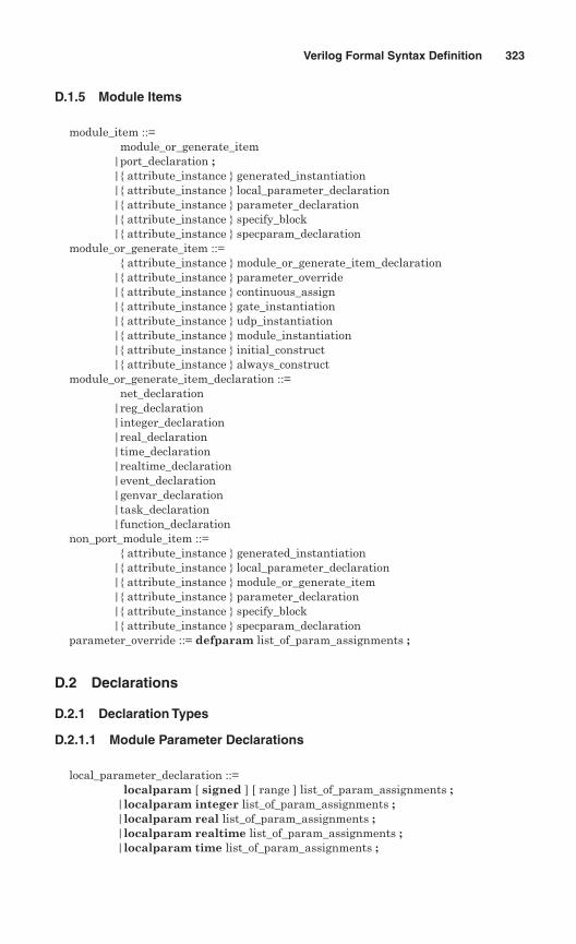
D.1.5 Module Items
module_item ::=module_or_generate_item
|port_declaration ;|{ attribute_instance } generated_instantiation|{ attribute_instance } local_parameter_declaration|{ attribute_instance } parameter_declaration|{ attribute_instance } specify_block|{ attribute_instance } specparam_declaration
module_or_generate_item ::={ attribute_instance } module_or_generate_item_declaration
|{ attribute_instance } parameter_override|{ attribute_instance } continuous_assign|{ attribute_instance } gate_instantiation|{ attribute_instance } udp_instantiation|{ attribute_instance } module_instantiation|{ attribute_instance } initial_construct|{ attribute_instance } always_construct
module_or_generate_item_declaration ::=net_declaration
|reg_declaration|integer_declaration|real_declaration|time_declaration|realtime_declaration|event_declaration|genvar_declaration|task_declaration|function_declaration
non_port_module_item ::={ attribute_instance } generated_instantiation
|{ attribute_instance } local_parameter_declaration|{ attribute_instance } module_or_generate_item|{ attribute_instance } parameter_declaration|{ attribute_instance } specify_block|{ attribute_instance } specparam_declaration
parameter_override ::= defparam list_of_param_assignments ;
D.2 Declarations
D.2.1 Declaration Types
D.2.1.1 Module Parameter Declarations
local_parameter_declaration ::=localparam [ signed ] [ range ] list_of_param_assignments ;
|localparam integer list_of_param_assignments ;|localparam real list_of_param_assignments ;|localparam realtime list_of_param_assignments ;|localparam time list_of_param_assignments ;
Verilog Formal Syntax Definition 323
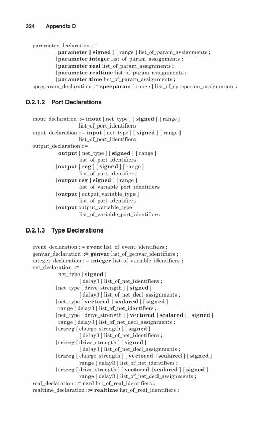
parameter_declaration ::=parameter [ signed ] [ range ] list_of_param_assignments ;
|parameter integer list_of_param_assignments ;|parameter real list_of_param_assignments ;|parameter realtime list_of_param_assignments ;|parameter time list_of_param_assignments ;
specparam_declaration ::= specparam [ range ] list_of_specparam_assignments ;
D.2.1.2 Port Declarations
inout_declaration ::= inout [ net_type ] [ signed ] [ range ]list_of_port_identifiers
input_declaration ::= input [ net_type ] [ signed ] [ range ]list_of_port_identifiers
output_declaration ::=output [ net_type ] [ signed ] [ range ]
list_of_port_identifiers|output [ reg ] [ signed ] [ range ]
list_of_port_identifiers|output reg [ signed ] [ range ]
list_of_variable_port_identifiers|output [ output_variable_type ]
list_of_port_identifiers|output output_variable_type
list_of_variable_port_identifiers
D.2.1.3 Type Declarations
event_declaration ::= event list_of_event_identifiers ;genvar_declaration ::= genvar list_of_genvar_identifiers ;integer_declaration ::= integer list_of_variable_identifiers ;net_declaration ::=
net_type [ signed ][ delay3 ] list_of_net_identifiers ;
|net_type [ drive_strength ] [ signed ][ delay3 ] list_of_net_decl_assignments ;
|net_type [ vectored |scalared ] [ signed ]range [ delay3 ] list_of_net_identifiers ;
|net_type [ drive_strength ] [ vectored |scalared ] [ signed ]range [ delay3 ] list_of_net_decl_assignments ;
|trireg [ charge_strength ] [ signed ][ delay3 ] list_of_net_identifiers ;
|trireg [ drive_strength ] [ signed ][ delay3 ] list_of_net_decl_assignments ;
|trireg [ charge_strength ] [ vectored |scalared ] [ signed ]range [ delay3 ] list_of_net_identifiers ;
|trireg [ drive_strength ] [ vectored |scalared ] [ signed ]range [ delay3 ] list_of_net_decl_assignments ;
real_declaration ::= real list_of_real_identifiers ;realtime_declaration ::= realtime list_of_real_identifiers ;
324 Appendix D
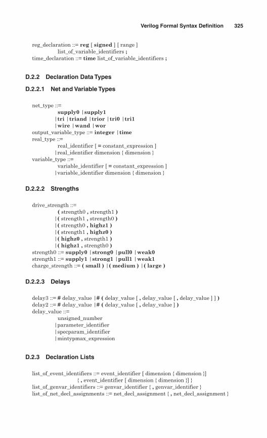
reg_declaration ::= reg [ signed ] [ range ]list_of_variable_identifiers ;
time_declaration ::= time list_of_variable_identifiers ;
D.2.2 Declaration Data Types
D.2.2.1 Net and Variable Types
net_type ::=supply0 |supply1
|tri |triand |trior |tri0 |tri1|wire |wand |wor
output_variable_type ::= integer |timereal_type ::=
real_identifier [ = constant_expression ]|real_identifier dimension { dimension }
variable_type ::=variable_identifier [ = constant_expression ]
|variable_identifier dimension { dimension }
D.2.2.2 Strengths
drive_strength ::=( strength0 , strength1 )
|( strength1 , strength0 )|( strength0 , highz1 )|( strength1 , highz0 )|( highz0 , strength1 )|( highz1 , strength0 )
strength0 ::= supply0 |strong0 |pull0 |weak0strength1 ::= supply1 |strong1 |pull1 |weak1charge_strength ::= ( small ) |( medium ) |( large )
D.2.2.3 Delays
delay3 ::= # delay_value |# ( delay_value [ , delay_value [ , delay_value ] ] )delay2 ::= # delay_value |# ( delay_value [ , delay_value ] )delay_value ::=
unsigned_number|parameter_identifier|specparam_identifier|mintypmax_expression
D.2.3 Declaration Lists
list_of_event_identifiers ::= event_identifier [ dimension { dimension }]{ , event_identifier [ dimension { dimension }] }
list_of_genvar_identifiers ::= genvar_identifier { , genvar_identifier }list_of_net_decl_assignments ::= net_decl_assignment { , net_decl_assignment }
Verilog Formal Syntax Definition 325
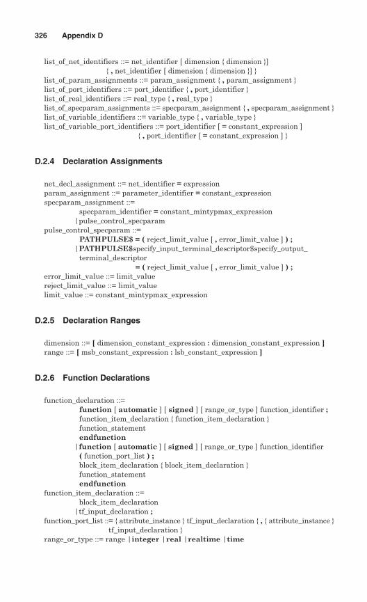
list_of_net_identifiers ::= net_identifier [ dimension { dimension }]{ , net_identifier [ dimension { dimension }] }
list_of_param_assignments ::= param_assignment { , param_assignment }list_of_port_identifiers ::= port_identifier { , port_identifier }list_of_real_identifiers ::= real_type { , real_type }list_of_specparam_assignments ::= specparam_assignment { , specparam_assignment }list_of_variable_identifiers ::= variable_type { , variable_type }list_of_variable_port_identifiers ::= port_identifier [ = constant_expression ]
{ , port_identifier [ = constant_expression ] }
D.2.4 Declaration Assignments
net_decl_assignment ::= net_identifier = expressionparam_assignment ::= parameter_identifier = constant_expressionspecparam_assignment ::=
specparam_identifier = constant_mintypmax_expression|pulse_control_specparam
pulse_control_specparam ::=PATHPULSE$ = ( reject_limit_value [ , error_limit_value ] ) ;
|PATHPULSE$specify_input_terminal_descriptor$specify_output_terminal_descriptor
= ( reject_limit_value [ , error_limit_value ] ) ;error_limit_value ::= limit_valuereject_limit_value ::= limit_valuelimit_value ::= constant_mintypmax_expression
D.2.5 Declaration Ranges
dimension ::= [ dimension_constant_expression : dimension_constant_expression ]range ::= [ msb_constant_expression : lsb_constant_expression ]
D.2.6 Function Declarations
function_declaration ::=function [ automatic ] [ signed ] [ range_or_type ] function_identifier ;function_item_declaration { function_item_declaration }function_statementendfunction
|function [ automatic ] [ signed ] [ range_or_type ] function_identifier( function_port_list ) ;block_item_declaration { block_item_declaration }function_statementendfunction
function_item_declaration ::=block_item_declaration
|tf_input_declaration ;function_port_list ::= { attribute_instance } tf_input_declaration { , { attribute_instance }
tf_input_declaration }range_or_type ::= range |integer |real |realtime |time
326 Appendix D
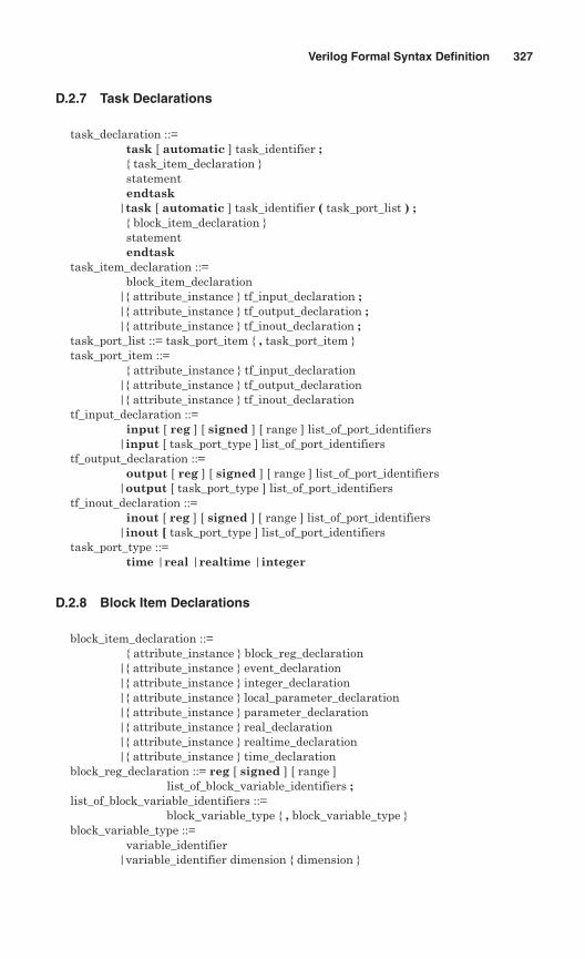
D.2.7 Task Declarations
task_declaration ::=task [ automatic ] task_identifier ;{ task_item_declaration }statementendtask
|task [ automatic ] task_identifier ( task_port_list ) ;{ block_item_declaration }statementendtask
task_item_declaration ::=block_item_declaration
|{ attribute_instance } tf_input_declaration ;|{ attribute_instance } tf_output_declaration ;|{ attribute_instance } tf_inout_declaration ;
task_port_list ::= task_port_item { , task_port_item }task_port_item ::=
{ attribute_instance } tf_input_declaration|{ attribute_instance } tf_output_declaration|{ attribute_instance } tf_inout_declaration
tf_input_declaration ::=input [ reg ] [ signed ] [ range ] list_of_port_identifiers
|input [ task_port_type ] list_of_port_identifierstf_output_declaration ::=
output [ reg ] [ signed ] [ range ] list_of_port_identifiers|output [ task_port_type ] list_of_port_identifiers
tf_inout_declaration ::=inout [ reg ] [ signed ] [ range ] list_of_port_identifiers
|inout [ task_port_type ] list_of_port_identifierstask_port_type ::=
time |real |realtime |integer
D.2.8 Block Item Declarations
block_item_declaration ::={ attribute_instance } block_reg_declaration
|{ attribute_instance } event_declaration|{ attribute_instance } integer_declaration|{ attribute_instance } local_parameter_declaration|{ attribute_instance } parameter_declaration|{ attribute_instance } real_declaration|{ attribute_instance } realtime_declaration|{ attribute_instance } time_declaration
block_reg_declaration ::= reg [ signed ] [ range ]list_of_block_variable_identifiers ;
list_of_block_variable_identifiers ::=block_variable_type { , block_variable_type }
block_variable_type ::=variable_identifier
|variable_identifier dimension { dimension }
Verilog Formal Syntax Definition 327
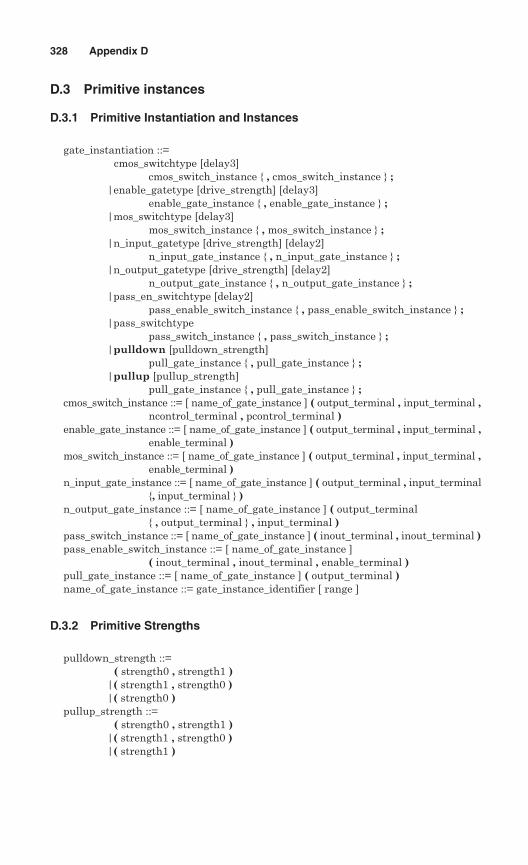
D.3 Primitive instances
D.3.1 Primitive Instantiation and Instances
gate_instantiation ::=cmos_switchtype [delay3]
cmos_switch_instance { , cmos_switch_instance } ;|enable_gatetype [drive_strength] [delay3]
enable_gate_instance { , enable_gate_instance } ;|mos_switchtype [delay3]
mos_switch_instance { , mos_switch_instance } ;|n_input_gatetype [drive_strength] [delay2]
n_input_gate_instance { , n_input_gate_instance } ;|n_output_gatetype [drive_strength] [delay2]
n_output_gate_instance { , n_output_gate_instance } ;|pass_en_switchtype [delay2]
pass_enable_switch_instance { , pass_enable_switch_instance } ;|pass_switchtype
pass_switch_instance { , pass_switch_instance } ;|pulldown [pulldown_strength]
pull_gate_instance { , pull_gate_instance } ;|pullup [pullup_strength]
pull_gate_instance { , pull_gate_instance } ;cmos_switch_instance ::= [ name_of_gate_instance ] ( output_terminal , input_terminal ,
ncontrol_terminal , pcontrol_terminal )enable_gate_instance ::= [ name_of_gate_instance ] ( output_terminal , input_terminal ,
enable_terminal )mos_switch_instance ::= [ name_of_gate_instance ] ( output_terminal , input_terminal ,
enable_terminal )n_input_gate_instance ::= [ name_of_gate_instance ] ( output_terminal , input_terminal
{, input_terminal } )n_output_gate_instance ::= [ name_of_gate_instance ] ( output_terminal
{ , output_terminal } , input_terminal )pass_switch_instance ::= [ name_of_gate_instance ] ( inout_terminal , inout_terminal )pass_enable_switch_instance ::= [ name_of_gate_instance ]
( inout_terminal , inout_terminal , enable_terminal )pull_gate_instance ::= [ name_of_gate_instance ] ( output_terminal )name_of_gate_instance ::= gate_instance_identifier [ range ]
D.3.2 Primitive Strengths
pulldown_strength ::=( strength0 , strength1 )
|( strength1 , strength0 )|( strength0 )
pullup_strength ::=( strength0 , strength1 )
|( strength1 , strength0 )|( strength1 )
328 Appendix D
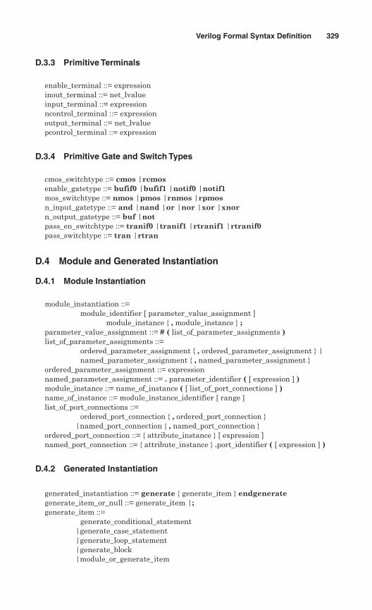
D.3.3 Primitive Terminals
enable_terminal ::= expressioninout_terminal ::= net_lvalueinput_terminal ::= expressionncontrol_terminal ::= expressionoutput_terminal ::= net_lvaluepcontrol_terminal ::= expression
D.3.4 Primitive Gate and Switch Types
cmos_switchtype ::= cmos |rcmosenable_gatetype ::= bufif0 |bufif1 |notif0 |notif1mos_switchtype ::= nmos |pmos |rnmos |rpmosn_input_gatetype ::= and |nand |or |nor |xor |xnorn_output_gatetype ::= buf |notpass_en_switchtype ::= tranif0 |tranif1 |rtranif1 |rtranif0pass_switchtype ::= tran |rtran
D.4 Module and Generated Instantiation
D.4.1 Module Instantiation
module_instantiation ::=module_identifier [ parameter_value_assignment ]
module_instance { , module_instance } ;parameter_value_assignment ::= # ( list_of_parameter_assignments )list_of_parameter_assignments ::=
ordered_parameter_assignment { , ordered_parameter_assignment } |named_parameter_assignment { , named_parameter_assignment }
ordered_parameter_assignment ::= expressionnamed_parameter_assignment ::= . parameter_identifier ( [ expression ] )module_instance ::= name_of_instance ( [ list_of_port_connections ] )name_of_instance ::= module_instance_identifier [ range ]list_of_port_connections ::=
ordered_port_connection { , ordered_port_connection }|named_port_connection { , named_port_connection }
ordered_port_connection ::= { attribute_instance } [ expression ]named_port_connection ::= { attribute_instance } .port_identifier ( [ expression ] )
D.4.2 Generated Instantiation
generated_instantiation ::= generate { generate_item } endgenerategenerate_item_or_null ::= generate_item |;generate_item ::=
generate_conditional_statement|generate_case_statement|generate_loop_statement|generate_block|module_or_generate_item
Verilog Formal Syntax Definition 329
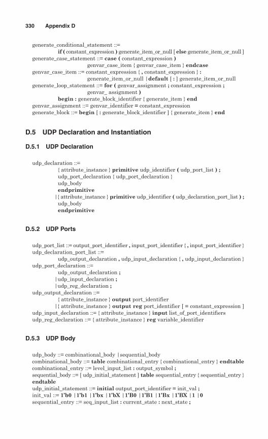
generate_conditional_statement ::=if ( constant_expression ) generate_item_or_null [ else generate_item_or_null ]
generate_case_statement ::= case ( constant_expression )genvar_case_item { genvar_case_item } endcase
genvar_case_item ::= constant_expression { , constant_expression } :generate_item_or_null |default [ : ] generate_item_or_null
generate_loop_statement ::= for ( genvar_assignment ; constant_expression ;genvar_ assignment )
begin : generate_block_identifier { generate_item } endgenvar_assignment ::= genvar_identifier = constant_expressiongenerate_block ::= begin [ : generate_block_identifier ] { generate_item } end
D.5 UDP Declaration and Instantiation
D.5.1 UDP Declaration
udp_declaration ::={ attribute_instance } primitive udp_identifier ( udp_port_list ) ;udp_port_declaration { udp_port_declaration }udp_bodyendprimitive
|{ attribute_instance } primitive udp_identifier ( udp_declaration_port_list ) ;udp_bodyendprimitive
D.5.2 UDP Ports
udp_port_list ::= output_port_identifier , input_port_identifier { , input_port_identifier }udp_declaration_port_list ::=
udp_output_declaration , udp_input_declaration { , udp_input_declaration }udp_port_declaration ::=
udp_output_declaration ;|udp_input_declaration ;|udp_reg_declaration ;
udp_output_declaration ::={ attribute_instance } output port_identifier
|{ attribute_instance } output reg port_identifier [ = constant_expression ]udp_input_declaration ::= { attribute_instance } input list_of_port_identifiersudp_reg_declaration ::= { attribute_instance } reg variable_identifier
D.5.3 UDP Body
udp_body ::= combinational_body |sequential_bodycombinational_body ::= table combinational_entry { combinational_entry } endtablecombinational_entry ::= level_input_list : output_symbol ;sequential_body ::= [ udp_initial_statement ] table sequential_entry { sequential_entry }endtableudp_initial_statement ::= initial output_port_identifier = init_val ;init_val ::= 1’b0 |1’b1 |1’bx |1’bX |1’B0 |1’B1 |1’Bx |1’BX |1 |0sequential_entry ::= seq_input_list : current_state : next_state ;
330 Appendix D
seq_input_list ::= level_input_list |edge_input_listlevel_input_list ::= level_symbol { level_symbol }edge_input_list ::= { level_symbol } edge_indicator { level_symbol }edge_indicator ::= ( level_symbol level_symbol ) |edge_symbolcurrent_state ::= level_symbolnext_state ::= output_symbol |-output_symbol ::= 0 |1 |x |Xlevel_symbol ::= 0 |1 |x |X |? |b |Bedge_symbol ::= r |R |f |F |p |P |n |N |*
D.5.4 UDP Instantiation
udp_instantiation ::= udp_identifier [ drive_strength ] [ delay2 ]udp_instance { , udp_instance } ;
udp_instance ::= [ name_of_udp_instance ] ( output_terminal , input_terminal{ , input_terminal } )
name_of_udp_instance ::= udp_instance_identifier [ range ]
D.6 Behavioral Statements
D.6.1 Continuous Assignment Statements
continuous_assign ::= assign [ drive_strength ] [ delay3 ] list_of_net_assignments ;list_of_net_assignments ::= net_assignment { , net_assignment }net_assignment ::= net_lvalue = expression
D.6.2 Procedural Blocks and Assignments
initial_construct ::= initial statementalways_construct ::= always statementblocking_assignment ::= variable_lvalue = [ delay_or_event_control ] expressionnonblocking_assignment ::= variable_lvalue <= [ delay_or_event_control ] expressionprocedural_continuous_assignments ::=
assign variable_assignment|deassign variable_lvalue|force variable_assignment|force net_assignment|release variable_lvalue|release net_lvalue
function_blocking_assignment ::= variable_lvalue = expressionfunction_statement_or_null ::=
function_statement|{ attribute_instance } ;
D.6.3 Parallel and Sequential Blocks
function_seq_block ::= begin [ : block_identifier{ block_item_declaration } ] { function_statement } end
variable_assignment ::= variable_lvalue = expression
Verilog Formal Syntax Definition 331
par_block ::= fork [ : block_identifier{ block_item_declaration } ] { statement } join
seq_block ::= begin [ : block_identifier{ block_item_declaration } ] { statement } end
D.6.4 Statements
statement ::={ attribute_instance } blocking_assignment ;
|{ attribute_instance } case_statement|{ attribute_instance } conditional_statement|{ attribute_instance } disable_statement|{ attribute_instance } event_trigger|{ attribute_instance } loop_statement|{ attribute_instance } nonblocking_assignment ;|{ attribute_instance } par_block|{ attribute_instance } procedural_continuous_assignments ;|{ attribute_instance } procedural_timing_control_statement|{ attribute_instance } seq_block|{ attribute_instance } system_task_enable|{ attribute_instance } task_enable|{ attribute_instance } wait_statement
statement_or_null ::=statement
|{ attribute_instance } ;function_statement ::=
{ attribute_instance } function_blocking_assignment ;|{ attribute_instance } function_case_statement|{ attribute_instance } function_conditional_statement|{ attribute_instance } function_loop_statement|{ attribute_instance } function_seq_block|{ attribute_instance } disable_statement|{ attribute_instance } system_task_enable
D.6.5 Timing Control Statements
delay_control ::=# delay_value
|# ( mintypmax_expression )delay_or_event_control ::=
delay_control|event_control|repeat ( expression ) event_control
disable_statement ::=disable hierarchical_task_identifier ;
|disable hierarchical_block_identifier ;event_control ::=
@ event_identifier|@ ( event_expression )|@*|@ (*)
332 Appendix D
event_trigger ::=−> hierarchical_event_identifier ;
event_expression ::=expression
|hierarchical_identifier|posedge expression|negedge expression|event_expression or event_expression|event_expression , event_expression
procedural_timing_control_statement ::=delay_or_event_control statement_or_null
wait_statement ::=wait ( expression ) statement_or_null
D.6.6 Conditional Statements
conditional_statement ::=if ( expression )
statement_or_null [ else statement_or_null ]|if_else_if_statement
if_else_if_statement ::=if ( expression ) statement_or_null{ else if ( expression ) statement_or_null }[ else statement_or_null ]
function_conditional_statement ::=if ( expression ) function_statement_or_null[ else function_statement_or_null ]
|function_if_else_if_statementfunction_if_else_if_statement ::=
if ( expression ) function_statement_or_null{ else if ( expression ) function_statement_or_null }[ else function_statement_or_null ]
D.6.7 Case Statements
case_statement ::=case ( expression )
case_item { case_item } endcase|casez ( expression )
case_item { case_item } endcase|casex ( expression )
case_item { case_item } endcasecase_item ::=
expression { , expression } : statement_or_null|default [ : ] statement_or_null
function_case_statement ::=case ( expression )
function_case_item { function_case_item } endcase|casez ( expression )
function_case_item { function_case_item } endcase
Verilog Formal Syntax Definition 333
|casex ( expression )function_case_item { function_case_item } endcase
function_case_item ::=expression { , expression } : function_statement_or_null
|default [ : ] function_statement_or_null
D.6.8 Looping Statements
function_loop_statement ::=forever function_statement
|repeat ( expression ) function_statement|while ( expression ) function_statement|for ( variable_assignment ; expression ; variable_assignment )
function_statementloop_statement ::=
forever statement|repeat ( expression ) statement|while ( expression ) statement|for ( variable_assignment ; expression ; variable_assignment )
statement
D.6.9 Task Enable Statements
system_task_enable ::= system_task_identifier [ ( expression { , expression } ) ] ;task_enable ::= hierarchical_task_identifier [ ( expression { , expression } ) ] ;
D.7 Specify Section
D.7.1 Specify Block Declaration
specify_block ::= specify { specify_item } endspecifyspecify_item ::=
specparam_declaration|pulsestyle_declaration|showcancelled_declaration|path_declaration|system_timing_check
pulsestyle_declaration ::=pulsestyle_onevent list_of_path_outputs ;
|pulsestyle_ondetect list_of_path_outputs ;showcancelled_declaration ::=
showcancelled list_of_path_outputs ;|noshowcancelled list_of_path_outputs ;
D.7.2 Specify Path Declarations
path_declaration ::=simple_path_declaration ;
334 Appendix D
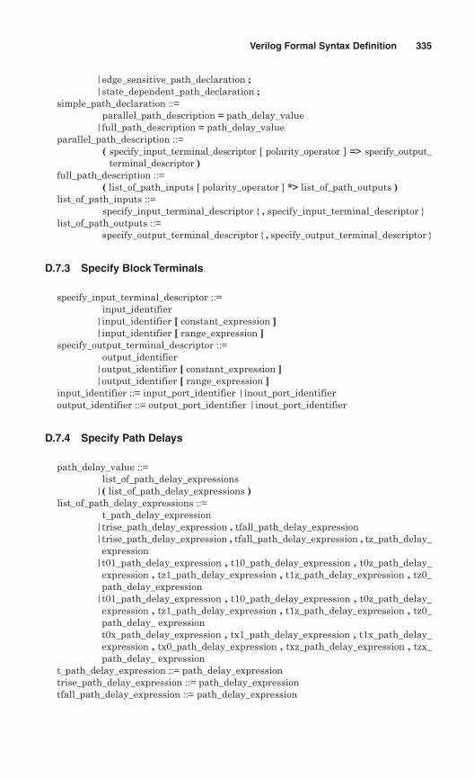
|edge_sensitive_path_declaration ;|state_dependent_path_declaration ;
simple_path_declaration ::=parallel_path_description = path_delay_value
|full_path_description = path_delay_valueparallel_path_description ::=
( specify_input_terminal_descriptor [ polarity_operator ] => specify_output_terminal_descriptor )
full_path_description ::=( list_of_path_inputs [ polarity_operator ] *> list_of_path_outputs )
list_of_path_inputs ::=specify_input_terminal_descriptor { , specify_input_terminal_descriptor }
list_of_path_outputs ::=specify_output_terminal_descriptor { , specify_output_terminal_descriptor }
D.7.3 Specify Block Terminals
specify_input_terminal_descriptor ::=input_identifier
|input_identifier [ constant_expression ]|input_identifier [ range_expression ]
specify_output_terminal_descriptor ::=output_identifier
|output_identifier [ constant_expression ]|output_identifier [ range_expression ]
input_identifier ::= input_port_identifier |inout_port_identifieroutput_identifier ::= output_port_identifier |inout_port_identifier
D.7.4 Specify Path Delays
path_delay_value ::=list_of_path_delay_expressions
|( list_of_path_delay_expressions )list_of_path_delay_expressions ::=
t_path_delay_expression|trise_path_delay_expression , tfall_path_delay_expression|trise_path_delay_expression , tfall_path_delay_expression , tz_path_delay_
expression|t01_path_delay_expression , t10_path_delay_expression , t0z_path_delay_
expression , tz1_path_delay_expression , t1z_path_delay_expression , tz0_path_delay_expression
|t01_path_delay_expression , t10_path_delay_expression , t0z_path_delay_expression , tz1_path_delay_expression , t1z_path_delay_expression , tz0_path_delay_ expressiont0x_path_delay_expression , tx1_path_delay_expression , t1x_path_delay_expression , tx0_path_delay_expression , txz_path_delay_expression , tzx_path_delay_ expression
t_path_delay_expression ::= path_delay_expressiontrise_path_delay_expression ::= path_delay_expressiontfall_path_delay_expression ::= path_delay_expression
Verilog Formal Syntax Definition 335
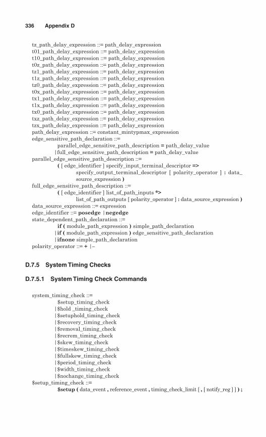
tz_path_delay_expression ::= path_delay_expressiont01_path_delay_expression ::= path_delay_expressiont10_path_delay_expression ::= path_delay_expressiont0z_path_delay_expression ::= path_delay_expressiontz1_path_delay_expression ::= path_delay_expressiont1z_path_delay_expression ::= path_delay_expressiontz0_path_delay_expression ::= path_delay_expressiont0x_path_delay_expression ::= path_delay_expressiontx1_path_delay_expression ::= path_delay_expressiont1x_path_delay_expression ::= path_delay_expressiontx0_path_delay_expression ::= path_delay_expressiontxz_path_delay_expression ::= path_delay_expressiontzx_path_delay_expression ::= path_delay_expressionpath_delay_expression ::= constant_mintypmax_expressionedge_sensitive_path_declaration ::=
parallel_edge_sensitive_path_description = path_delay_value|full_edge_sensitive_path_description = path_delay_value
parallel_edge_sensitive_path_description ::=( [ edge_identifier ] specify_input_terminal_descriptor =>
specify_output_terminal_descriptor [ polarity_operator ] : data_source_expression )
full_edge_sensitive_path_description ::=( [ edge_identifier ] list_of_path_inputs *>
list_of_path_outputs [ polarity_operator ] : data_source_expression )data_source_expression ::= expressionedge_identifier ::= posedge |negedgestate_dependent_path_declaration ::=
if ( module_path_expression ) simple_path_declaration|if ( module_path_expression ) edge_sensitive_path_declaration|ifnone simple_path_declaration
polarity_operator ::= + |–
D.7.5 System Timing Checks
D.7.5.1 System Timing Check Commands
system_timing_check ::=$setup_timing_check
|$hold _timing_check|$setuphold_timing_check|$recovery_timing_check|$removal_timing_check|$recrem_timing_check|$skew_timing_check|$timeskew_timing_check|$fullskew_timing_check|$period_timing_check|$width_timing_check|$nochange_timing_check
$setup_timing_check ::=$setup ( data_event , reference_event , timing_check_limit [ , [ notify_reg ] ] ) ;
336 Appendix D
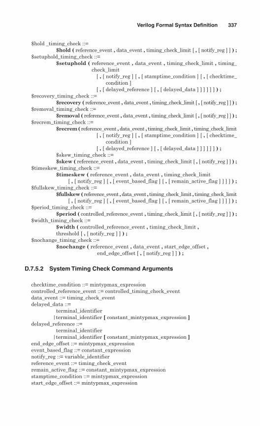
$hold _timing_check ::=$hold ( reference_event , data_event , timing_check_limit [ , [ notify_reg ] ] ) ;
$setuphold_timing_check ::=$setuphold ( reference_event , data_event , timing_check_limit , timing_
check_limit[ , [ notify_reg ] [ , [ stamptime_condition ] [ , [ checktime_
condition ][ , [ delayed_reference ] [ , [ delayed_data ] ] ] ] ] ] ) ;
$recovery_timing_check ::=$recovery ( reference_event , data_event , timing_check_limit [ , [ notify_reg ] ] ) ;
$removal_timing_check ::=$removal ( reference_event , data_event , timing_check_limit [ , [ notify_reg ] ] ) ;
$recrem_timing_check ::=$recrem ( reference_event , data_event , timing_check_limit , timing_check_limit
[ , [ notify_reg ] [ , [ stamptime_condition ] [ , [ checktime_condition ]
[ , [ delayed_reference ] [ , [ delayed_data ] ] ] ] ] ] ) ;$skew_timing_check ::=$skew ( reference_event , data_event , timing_check_limit [ , [ notify_reg ] ] ) ;
$timeskew_timing_check ::=$timeskew ( reference_event , data_event , timing_check_limit
[ , [ notify_reg ] [ , [ event_based_flag ] [ , [ remain_active_flag ] ] ] ] ) ;$fullskew_timing_check ::=
$fullskew ( reference_event , data_event , timing_check_limit , timing_check_limit[ , [ notify_reg ] [ , [ event_based_flag ] [ , [ remain_active_flag ] ] ] ] ) ;
$period_timing_check ::=$period ( controlled_reference_event , timing_check_limit [ , [ notify_reg ] ] ) ;
$width_timing_check ::=$width ( controlled_reference_event , timing_check_limit ,threshold [ , [ notify_reg ] ] ) ;
$nochange_timing_check ::=$nochange ( reference_event , data_event , start_edge_offset ,
end_edge_offset [ , [ notify_reg ] ] ) ;
D.7.5.2 System Timing Check Command Arguments
checktime_condition ::= mintypmax_expressioncontrolled_reference_event ::= controlled_timing_check_eventdata_event ::= timing_check_eventdelayed_data ::=
terminal_identifier|terminal_identifier [ constant_mintypmax_expression ]
delayed_reference ::=terminal_identifier
|terminal_identifier [ constant_mintypmax_expression ]end_edge_offset ::= mintypmax_expressionevent_based_flag ::= constant_expressionnotify_reg ::= variable_identifierreference_event ::= timing_check_eventremain_active_flag ::= constant_mintypmax_expressionstamptime_condition ::= mintypmax_expressionstart_edge_offset ::= mintypmax_expression
Verilog Formal Syntax Definition 337
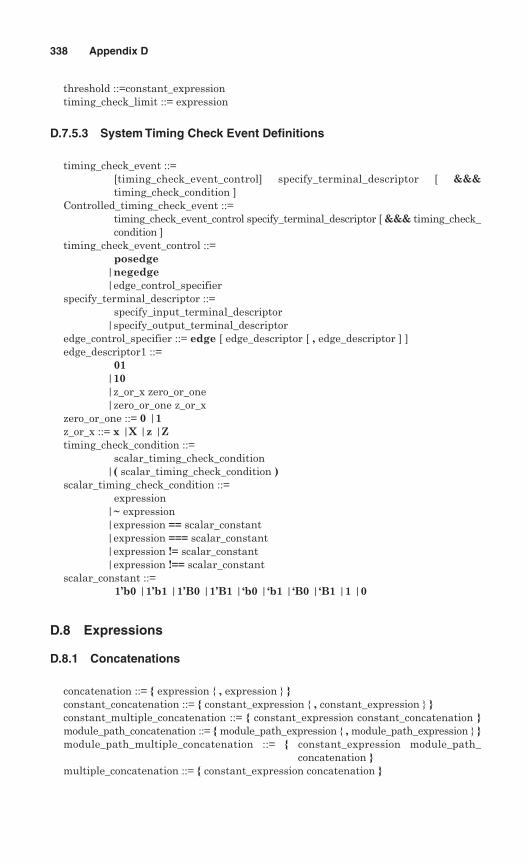
threshold ::=constant_expressiontiming_check_limit ::= expression
D.7.5.3 System Timing Check Event Definitions
timing_check_event ::=[timing_check_event_control] specify_terminal_descriptor [ &&&timing_check_condition ]
Controlled_timing_check_event ::=timing_check_event_control specify_terminal_descriptor [ &&& timing_check_condition ]
timing_check_event_control ::=posedge
|negedge|edge_control_specifier
specify_terminal_descriptor ::=specify_input_terminal_descriptor
|specify_output_terminal_descriptoredge_control_specifier ::= edge [ edge_descriptor [ , edge_descriptor ] ]edge_descriptor1 ::=
01|10|z_or_x zero_or_one|zero_or_one z_or_x
zero_or_one ::= 0 |1z_or_x ::= x |X |z |Ztiming_check_condition ::=
scalar_timing_check_condition|( scalar_timing_check_condition )
scalar_timing_check_condition ::=expression
|~ expression|expression == scalar_constant|expression === scalar_constant|expression != scalar_constant|expression !== scalar_constant
scalar_constant ::=1’b0 |1’b1 |1’B0 |1’B1 |‘b0 |‘b1 |‘B0 |‘B1 |1 |0
D.8 Expressions
D.8.1 Concatenations
concatenation ::= { expression { , expression } }constant_concatenation ::= { constant_expression { , constant_expression } }constant_multiple_concatenation ::= { constant_expression constant_concatenation }module_path_concatenation ::= { module_path_expression { , module_path_expression } }module_path_multiple_concatenation ::= { constant_expression module_path_
concatenation }multiple_concatenation ::= { constant_expression concatenation }
338 Appendix D
net_concatenation ::= { net_concatenation_value { , net_concatenation_value } }net_concatenation_value ::=
hierarchical_net_identifier|hierarchical_net_identifier [ expression ] { [ expression ] }|hierarchical_net_identifier [ expression ] { [ expression ] } [ range_expression ]|hierarchical_net_identifier [ range_expression ]|net_concatenation
variable_concatenation ::= { variable_concatenation_value { , variable_concatenation_value } }variable_concatenation_value ::=
hierarchical_variable_identifier|hierarchical_variable_identifier [ expression ] { [ expression ] }|hierarchical_variable_identifier [ expression ] { [ expression ] } [ range_
expression ]|hierarchical_variable_identifier [ range_expression ]|variable_concatenation
D.8.2 Function Calls
constant_function_call ::= function_identifier { attribute_instance }( constant_expression { , constant_expression } )
function_call ::= hierarchical_function_identifier { attribute_instance }( expression { , expression } )
genvar_function_call ::= genvar_function_identifier { attribute_instance }( constant_expression { , constant_expression } )
system_function_call ::= system_function_identifier[ ( expression { , expression } ) ]
D.8.3 Expressions
base_expression ::= expressionconditional_expression ::= expression1 ? { attribute_instance } expression2 : expression3constant_base_expression ::= constant_expressionconstant_expression ::=
constant_primary|unary_operator { attribute_instance } constant_primary|constant_expression binary_operator { attribute_instance } constant_expression|constant_expression ? { attribute_instance } constant_expression : constant_
expression|string
constant_mintypmax_expression ::=constant_expression
|constant_expression : constant_expression : constant_expressionconstant_range_expression ::=
constant_expression|msb_constant_expression : lsb_constant_expression|constant_base_expression +: width_constant_expression|constant_base_expression -: width_constant_expression
dimension_constant_expression ::= constant_expressionexpression1 ::= expressionexpression2 ::= expression
Verilog Formal Syntax Definition 339
expression3 ::= expressionexpression ::=
primary|unary_operator { attribute_instance } primary|expression binary_operator { attribute_instance } expression|conditional_expression|string
lsb_constant_expression ::= constant_expressionmintypmax_expression ::=
expression|expression : expression : expression
module_path_conditional_expression ::= module_path_expression ? { attribute_instance }module_path_expression : module_path_expression
module_path_expression ::=module_path_primary
|unary_module_path_operator { attribute_instance } module_path_primary|module_path_expression binary_module_path_operator { attribute_instance }
module_path_expression|module_path_conditional_expression
module_path_mintypmax_expression ::=module_path_expression
|module_path_expression : module_path_expression : module_path_expressionmsb_constant_expression ::= constant_expressionrange_expression ::=
expression|msb_constant_expression : lsb_constant_expression|base_expression +: width_constant_expression|base_expression -: width_constant_expression
width_constant_expression ::= constant_expression
D.8.4 Primaries
constant_primary ::=constant_concatenation
|constant_function_call|( constant_mintypmax_expression )|constant_multiple_concatenation|genvar_identifier|number|parameter_identifier|specparam_identifier
module_path_primary ::=number
|identifier|module_path_concatenation|module_path_multiple_concatenation|function_call|system_function_call|constant_function_call|( module_path_mintypmax_expression )
primary ::=number
340 Appendix D
|hierarchical_identifier|hierarchical_identifier [ expression ] { [ expression ] }|hierarchical_identifier [ expression ] { [ expression ] } [ range_expression ]|hierarchical_identifier [ range_expression ]|concatenation|multiple_concatenation|function_call|system_function_call|constant_function_call|( mintypmax_expression )
D.8.5 Expression Left-Side Values
net_lvalue ::=hierarchical_net_identifier
|hierarchical_net_identifier [ constant_expression ] { [ constant_expression ] }|hierarchical_net_identifier [ constant_expression ] { [ constant_expression ] } [
constant_range_expression ]|hierarchical_net_identifier [ constant_range_expression ]|net_concatenation
variable_lvalue ::=hierarchical_variable_identifier
|hierarchical_variable_identifier [ expression ] { [ expression ] }|hierarchical_variable_identifier [ expression ] { [ expression ] } [ range_
expression ]|hierarchical_variable_identifier [ range_expression ]|variable_concatenation
D.8.6 Operators
unary_operator ::=+|--|!|~|&|~& |||~||^|~^|^~
binary_operator ::=+|--|*|/|%|==|!=|===|!==|&&||||**
|<|<= |>|>=|&|||^|^~|~^|>>|<<|>>>|<<<unary_module_path_operator ::=
!|~|&|~&|||~||^|~^|^~binary_module_path_operator ::=
==|!=|&&||||&|||^|^~|~^
D.8.7 Numbers
number ::=decimal_number
|octal_number|binary_number|hex_number|real_number
real_number1 ::=unsigned_number . unsigned_number
Verilog Formal Syntax Definition 341
|unsigned_number [ . unsigned_number ] exp [ sign ] unsigned_numberexp ::= e |Edecimal_number ::=
unsigned_number|[ size ] decimal_base unsigned_number|[ size ] decimal_base x_digit { _ }|[ size ] decimal_base z_digit { _ }
binary_number ::= [ size ] binary_base binary_valueoctal_number ::= [ size ] octal_base octal_valuehex_number ::= [ size ] hex_base hex_valuesign ::= + |--size ::= non_zero_unsigned_numbernon_zero_unsigned_number1 ::= non_zero_decimal_digit { _ |decimal_digit}unsigned_number1 ::= decimal_digit { _ |decimal_digit }binary_value1 ::= binary_digit { _ |binary_digit }octal_value1 ::= octal_digit { _ |octal_digit }hex_value1 ::= hex_digit { _ |hex_digit }decimal_base1 ::= ’[s|S]d |’[s|S]Dbinary_base1 ::= ’[s|S]b |’[s|S]Boctal_base1 ::= ’[s|S]o |’[s|S]Ohex_base1 ::= ’[s|S]h |’[s|S]Hnon_zero_decimal_digit ::= 1 |2 |3 |4 |5 |6 |7 |8 |9decimal_digit ::= 0 |1 |2 |3 |4 |5 |6 |7 |8 |9binary_digit ::= x_digit |z_digit |0 |1octal_digit ::= x_digit |z_digit |0 |1 |2 |3 |4 |5 |6 |7hex_digit ::=
x_digit |z_digit |0 |1 |2 |3 |4 |5 |6 |7 |8 |9|a |b |c |d |e |f |A |B |C |D |E |F
x_digit ::= x |Xz_digit ::= z |Z |?
D.8.8 Strings
string ::= “ { Any_ASCII_Characters_except_new_line } ”
D.9 General
D.9.1 Attributes
attribute_instance ::= (* attr_spec { , attr_spec } *)attr_spec ::=
attr_name = constant_expression|attr_name
attr_name ::= identifier
D.9.2 Comments
comment ::=one_line_comment
|block_comment
342 Appendix D
one_line_comment ::= // comment_text \nblock_comment ::= /* comment_text */comment_text ::= { Any_ASCII_character }
D.9.3 Identifiers
arrayed_identifier ::=simple_arrayed_identifier
|escaped_arrayed_identifierblock_identifier ::= identifiercell_identifier ::= identifierconfig_identifier ::= identifierescaped_arrayed_identifier ::= escaped_identifier [ range ]escaped_hierarchical_identifier4 ::=
escaped_hierarchical_branch{ .simple_hierarchical_branch |.escaped_hierarchical_branch }
escaped_identifier ::= \ {Any_ASCII_character_except_white_space} white_spaceevent_identifier ::= identifierfunction_identifier ::= identifiergate_instance_identifier ::= arrayed_identifiergenerate_block_identifier ::= identifiergenvar_function_identifier ::= identifier /* Hierarchy disallowed */genvar_identifier ::= identifierhierarchical_block_identifier ::= hierarchical_identifierhierarchical_event_identifier ::= hierarchical_identifierhierarchical_function_identifier ::= hierarchical_identifierhierarchical_identifier ::=
simple_hierarchical_identifier|escaped_hierarchical_identifier
hierarchical_net_identifier ::= hierarchical_identifierhierarchical_variable_identifier ::= hierarchical_identifierhierarchical_task_identifier ::= hierarchical_identifieridentifier ::=
simple_identifier|escaped_identifier
inout_port_identifier ::= identifierinput_port_identifier ::= identifierinstance_identifier ::= identifierlibrary_identifier ::= identifiermemory_identifier ::= identifiermodule_identifier ::= identifiermodule_instance_identifier ::= arrayed_identifiernet_identifier ::= identifieroutput_port_identifier ::= identifierparameter_identifier ::= identifierport_identifier ::= identifierreal_identifier ::= identifiersimple_arrayed_identifier ::= simple_identifier [ range ]simple_hierarchical_identifier3 ::=
simple_hierarchical_branch [ .escaped_identifier ]simple_identifier2 ::= [ a-zA-Z_ ] { [ a-zA-Z0-9_$ ] }specparam_identifier ::= identifier
Verilog Formal Syntax Definition 343
system_function_identifier5 ::= $[ a-zA-Z0-9_$ ]{ [ a-zA-Z0-9_$ ] }system_task_identifier5 ::= $[ a-zA-Z0-9_$ ]{ [ a-zA-Z0-9_$ ] }task_identifier ::= identifierterminal_identifier ::= identifiertext_macro_identifier ::= simple_identifiertopmodule_identifier ::= identifierudp_identifier ::= identifierudp_instance_identifier ::= arrayed_identifiervariable_identifier ::= identifier
D.9.4 Identifier Branches
simple_hierarchical_branch3 ::=simple_identifier [ [ unsigned_number ] ]
[ { .simple_identifier [ [ unsigned_number ] ] } ]escaped_hierarchical_branch4 ::=
escaped_identifier [ [ unsigned_number ] ][ { .escaped_identifier [ [ unsigned_number ] ] } ]
D.9.5 White Space
white_space ::= space |tab |newline |eof6
Notes
1. Embedded spaces are illegal.
2. A simple_identifier and arrayed_reference shall start with an alphaor underscore (_) character, shall have at least one character, andshall not have any spaces.
3. The period (.) in simple_hierarchical_identifier and simple_hierarchi-cal_branch shall not be preceded or followed by white_space.
4. The period in escaped_hierarchical_identifier and escaped_hierarchi-cal_branch shall be preceded by white_space, but shall not be followedby white_space.
5. The $ character in a system_function_identifier or system_task_iden-tifier shall not be followed by white_space. A system_function_iden-tifier or system_task_identifier shall not be escaped.
6. End of file.
344 Appendix D
Appendix
EVerilog Assertion Monitors
OVL assertion checkers are Verilog modules with parameters and portsthat can be used to check the occurrence of certain conditions in a design.The assertion library must be installed in order to be used with a Verilogsimulation program. The Accelera Standard OVL V1.0 document in theaccompanying CD of this book has details of OVL library installation andusage. Timing diagrams and examples in this document provide a com-prehensive document for proper use of this library by Verilog designers.This appendix serves as a quick reference for OVL assertion checkersand does not include installation and detailed analysis contained in theAccelera document.
An OVL assertion checker is invoked by a set of optional parametersand a set of ports (arguments) that provide conditions that lead to check-ing what is referred to as the checker’s test expression. A set of integervalues have been defined for the checkers’ optional parameters. When theOVL library is installed, the Verilog `define construct is used for associ-ating integer constants with meaningful variable names. Variables usedfor assertion parameters and their corresponding values are as follows:
// a c t i v e e d g e s`define OVL_NOEDGE 0`define OVL_POSEDGE 1`define OVL_NEGEDGE 2`define OVL_ANYEDGE 3
// s e v e r i t y l e v e l s`define OVL_FATAL 0`define OVL_ERROR 1`define OVL_WARNING 2`define OVL_INFO 3
345
Copyright © 2006 by The McGraw-Hill Publishing Companies, Inc. Click here for terms of use.
// c o v e r a g e l e v e l s`define OVL_COVER_NONE 0`define OVL_COVER_ALL 1
// p r o p e r t y t y p e`define OVL_ASSERT 0`define OVL_ASSUME 1
// n e c e s s a r y c o n d i t i o n`define OVL_TRIGGER_ON_MOST_PIPE 0`define OVL_TRIGGER_ON_FIRST_PIPE 1`define OVL_TRIGGER_ON_FIRST_NOPIPE 2
// a c t i o n o n n e w s t a r t`define OVL_IGNORE_NEW_START 0`define OVL_RESET_ON_NEW_START 1`define OVL_ERROR_ON_NEW_START 2
// i n a c t i v e l e v e l s`define OVL_ALL_ZEROS 0`define OVL_ALL_ONES 1`define OVL_ONE_COLD 2
In the sections that follow we will give a brief description of OVLassertion checkers. Parameters and ports (arguments) of each are dis-cussed here.
E.1 assert_always
The assert_always assertion checker evaluates the expression test_exprat every positive edge of the triggering event or clock clk. This assertioncontends that the expression always evaluates to TRUE. Should theexpression evaluate to FALSE, the message msg will be reported withseverity severity_level.
assert_always#( severity_level, property_type, msg, coverage_level ) instance_name ( clk, reset_n, test_expr )
� severity_level is for handling an assertion violation. The values areOVL_FATAL, OVL_ERROR, OVL_WARNING, or OVL_INFO. Thedefault value is OVL_ERROR.
� property_type determines whether to use the assertion as an assertproperty or an assume property. The default value is OVL_ASSERT.
346 Appendix E
Verilog Assertion Monitors 347
� msg is a string expression displayed whenever the assertion fails. Ithas a language-dependent default value.
� coverage_level is for enabling or disabling coverage monitoring for thechecker. The default value is OVL_COVERALL.
� clk is a signal whose positive edge triggers the checking of the asser-tion.
� reset_n is a signal, that when deasserted, indicates that the assertionis to be monitored.
� test_expr is the expression being monitored by this instance ofassert_always.
E.2 assert_always_on_edge
The assert_always_on_edge assertion checker monitors the test_exprat every specified edge of the sampling event and positive edge of clockclk. It contends that a specified expression will always evaluate to TRUEon the edge of a sampling event. Whenever test_expr evaluates toFALSE, the message msg will be reported with the severity_level.
assert_always_on_edge#( severity_level, edge_type, property_type,
msg, coverage_level ) instance_name (clk, reset_n, sampling_event, test_expr )
� severity_level is for handling an assertion violation. The values areOVL_FATAL, OVL_ERROR, OVL_WARNING, or OVL_INFO. Thedefault value is OVL_ERROR.
� edge_type determines which type of transition of sampling_event ini-tiates the check.� `OVL_POSEDGE, initiates the check if sampling_event transitions
to 1. � `OVL_NEGEDGE, initiates the check if sampling_event transitions
to 0. � `OVL_POSEDGE, initiates the check if sampling_event transitions
to 1 or to 0. � `OVL_NOEDGE (default), always initiates the check and sam-
pling_event is never sampled. � property_type determines whether to use the assertion as an assert
property or an assume property. The default value is OVL_ASSERT.
� msg is a string expression displayed whenever the assertion fails. Ithas a language-dependent default value.
� coverage_level is for enabling or disabling coverage monitoring for thechecker. The default value is OVL_COVERALL.
� clk is a signal whose positive edge triggers the checking of the asser-tion, provided that an edge of the type indicated by edge type simul-taneously occurs on the sampling event.
� reset_n is a signal, that when deasserted, indicates that the assertionis to be monitored.
� sampling_event is an boolean expression, that when TRUE, enablesthe monitoring of test_expr.
� test_expr is the expression being monitored by this instance ofassert_always_on_edge.
E.3 assert_change
The assert_change assertion monitors the start_event at every positiveedge of the start event or positive edge of clock clk. It contends that thetest expression will change value within num_cks clock cycles. If this con-dition does not hold, the message msg will be reported with severity_level.
assert_change#( severity_level, width, num_cks, action_on_new_start,
property_type, msg, coverage_level )instance_name (clk, reset_n, start_event, test_expr)
� severity_level is for handling an assertion violation. The values areOVL_FATAL, OVL_ERROR, OVL_WARNING, or OVL_INFO. Thedefault value is OVL_ERROR.
� width is the width of test_expr, with a default of 1.� num_cks is the number of clock cycles within which test_expr is to
change.� action_on_new_start is the method of handling a new start that occurs
before test_expr changes value or num_cks cycles transpire without achange.� `OVL_IGNORE_NEW_START (default), ignores all assertions of
start_event after the first assertion has been detected.� `OVL_RESET_ON_NEW_START, restart monitoring of test_expr if
start_event is asserted in any subsequent clock assertion duringthe monitoring of test_expr.
348 Appendix E
� `OVL_ERROR_ON_NEW_START, while monitoring, issue an errorif start_event is asserted in any clock cycle subsequent to the cyclein which monitoring began.
� property_type determines whether to use the assertion as an assertproperty or an assume property. The default value is OVL_ASSERT.
� msg is a string expression displayed whenever the assertion fails. Ithas a language-dependent default value.
� coverage_level is for enabling or disabling coverage monitoring for thechecker. The default value is OVL_COVERALL.
� clk is a signal whose positive edge triggers the checking of the asser-tion.
� reset_n is a signal, that when deasserted, indicates that the assertionis to be monitored.
� start_event Starting event that triggers the monitoring of test_expr.� test_expr the expression being monitored by this instance of
assert_change.
E.4 assert_cycle_sequence
The assert_cycle_sequence assertion contends that a specifiedsequence of events occurs. It checks sequences in three ways:
� If necessary_condition is ̀ OVL_TRIGGER_ON_MOST_PIPE (default),it contends that, if the first num_cks-1 events of event_sequence occurin sequence, then the final one (event_sequence(0)) also occurs.
� If necessary_condition is `OVL_TRIGGER_ON_FIRST_PIPE, it con-tends that once the first event (event_sequence(num_cks-1)) occurs, allthe remaining events also occur in sequence. This allows simultane-ous checking to run, i.e., overlapping of correct sequences is allowed.
� If necessary_condition is `OVL_TRIGGER_ON_FIRST_NOPIPE, itcontends that once the first event (event_sequence(num_cks-1)) occurs,all the remaining events also occur in sequence. This does not allowa new checking to begin so long as another checking is in progress, i.e.,no overlapping is allowed and one sequence has to be completed beforethe next checking begins.
assert_cycle_sequence#( severity_level, num_cks, necessary_condition,
property_type, msg, coverage_level )instance_name (clk, reset_n, event_sequence)
Verilog Assertion Monitors 349
� severity_level is for handling an assertion violation. The values areOVL_FATAL, OVL_ERROR, OVL_WARNING, or OVL_INFO. Thedefault value is OVL_ERROR.
� num_cks The number of events in the event_sequence (and the lengthof the event_sequence array).
� necessary_condition, either 0 or 1, with a default of 0.� property_type determines whether to use the assertion as an assert
property or an assume property. The default value is OVL_ASSERT.� msg is a string expression displayed whenever the assertion fails. It
has a language-dependent default value.� coverage_level is for enabling or disabling coverage monitoring for the
checker. The default value is OVL_COVERALL.� clk is a signal whose positive edge triggers the checking of the asser-
tion.� reset_n is a signal, that when deasserted, indicates that the assertion
is to be monitored.� event_sequence A Verilog or VHDL concatenation expression, where
each bit represents an event.
E.5 assert_decrement
The assert_decrement assertion checker monitors the expressiontest_expr at every positive edge of the clock clk. This assertion contendsthat the expression never decreases in value except in steps of value. Theexpression test_expr can be any valid integral expression. The checkbegins at the first rising edge of clk after reset_n is deasserted.
assert_decrement#( severity_level, width, value, property_type,
msg, coverage_level )instance_name ( clk, reset_n, test_expr )
� severity_level is for handling an assertion violation. The values areOVL_FATAL, OVL_ERROR, OVL_WARNING, or OVL_INFO. Thedefault value is OVL_ERROR.
� width is the width of the test expression (default value is 1).� value permitted decrement value (default value is 1).� property_type determines whether to use the assertion as an assert
property or an assume property. The default value is OVL_ASSERT.
350 Appendix E
� msg is a string expression displayed whenever the assertion fails. Ithas a language-dependent default value.
� coverage_level is for enabling or disabling coverage monitoring for thechecker. The default value is OVL_COVERALL.
� clk is a signal whose positive edge triggers the checking of the asser-tion.
� reset_n is a signal, that when deasserted, indicates that the assertionis to be monitored.
� test_expr[width-1:0] is the expression being monitored by this instanceof assert_decrement.
E.6 assert_delta
The assert_delta assertion monitors the expression test_expr at everypositive edge of the triggering event or clock clk. This assertion contendsthat the expression never changes value by less than the min value ormore than the max value.
assert_delta#( severity_level, width, min, max, property_type,
msg, coverage_level )instance_name ( clk, reset_n, test_expr )
� severity_level is for handling an assertion violation. The values areOVL_FATAL, OVL_ERROR, OVL_WARNING, or OVL_INFO. Thedefault value is OVL_ERROR.
� width is the width of the test expression (default value is 1).� min is the minimum value by which the test expression can change
in value in one step (default value is 1).� max is the maximum value by which the test expression can change
in value in one step (default value is 1).� property_type determines whether to use the assertion as an assert
property or an assume property. The default value is OVL_ASSERT.� msg is a string expression displayed whenever the assertion fails. It
has a language-dependent default value.� coverage_level is for enabling or disabling coverage monitoring for the
checker. The default value is OVL_COVERALL.� clk is a signal whose positive edge triggers the checking of the assertion.
Verilog Assertion Monitors 351
� reset_n is a signal, that when deasserted, indicates that the assertionis to be monitored.
� test_expr[width-1:0] is the expression being monitored by this instanceof assert_delta.
E.7 assert_even_parity
The assert_even_parity assertion monitors the expression test_expr atevery positive edge of the triggering event or clock clk. This assertioncontends that the expression always has an even number of bitsasserted.
assert_even_parity#( severity_level, width, property_type,
msg, coverage_level )instance_name ( clk, reset_n, test_expr )
� severity_level is for handling an assertion violation. The values areOVL_FATAL, OVL_ERROR, OVL_WARNING, or OVL_INFO. Thedefault value is OVL_ERROR.
� width is the width of the test expression (default value is 1).� property_type determines whether to use the assertion as an assert
property or an assume property. The default value is OVL_ASSERT.� msg is a string expression displayed whenever the assertion fails. It
has a language-dependent default value.� coverage_level is for enabling or disabling coverage monitoring for the
checker. The default value is OVL_COVERALL.� clk is a signal whose positive edge triggers the checking of the asser-
tion.� reset_n is a signal, that when deasserted, indicates that the assertion
is to be monitored.� test_expr[width-1:0] is the expression being monitored by this instance
of assert_even_parity.
E.8 assert_fifo_index
The assert_fifo_index assertion monitors the index of a FIFO-likestructure to assure that it never either overflows or underflows. Theassertion supports multiple pushes (writes) into and pops (reads) froma FIFO within a given clock cycle.
352 Appendix E
assert_fifo_index#( severity_level, depth, push_width, pop_width, property_type,
msg, coverage_level, simultaneous_push_pop )instance_name ( clk, reset_n, push, pop )
� severity_level is for handling an assertion violation. The values areOVL_FATAL, OVL_ERROR, OVL_WARNING, or OVL_INFO. Thedefault value is OVL_ERROR.
� depth is an integral expression specifying the maximum number of ele-ments the queue or FIFO can hold.
� push_width is an integral expression defining the maximum numberof pushes (or writes) that is possible in a single clock cycle. The defaultvalue is 1.
� pop_width is an integral expression defining the maximum numberof pops (or reads) that is possible in a single clock cycle. The defaultvalue is 1.
� property_type determines whether to use the assertion as an assertproperty or an assume property. The default value is OVL_ASSERT.
� msg is a string expression displayed whenever the assertion fails. Ithas a language-dependent default value.
� coverage_level is for enabling or disabling coverage monitoring for thechecker. The default value is OVL_COVERALL.
� clk is a signal whose positive edge triggers the checking of the assertion.� reset_n is a signal, that when deasserted, indicates that the assertion
is to be monitored.� Push[push_width-1:0] is an integral expression indicating the number
of pushes (writes) occurring in the current clock cycle, with a defaultvalue of 1.
� Pop[pop_width-1:0] is an integral expression indicating the numberof pops (reads) occurring in the current clock cycle, with a defaultvalue of 1.
E.9 assert_frame
The assert_frame assertion monitors the timing relationships betweentwo events in a sequence of events. When start_event is asserted,test_expr must evaluate to TRUE within a given range of clock cycles.
assert_frame#( severity_level, min_cks, max_cks, action_on_new_start,
property_type, msg, coverage_level) instance_name ( clk, reset_n, start_event, test_expr )
Verilog Assertion Monitors 353
� severity_level is for handling an assertion violation. The values areOVL_FATAL, OVL_ERROR, OVL_WARNING, or OVL_INFO. Thedefault value is OVL_ERROR.
� min_cks is the minimum number of clock cycles to wait afterstart_event is asserted (the first event in the sequence) for the test_exprto be asserted (the second event in the sequence). If 0, there is no min-imum number of cycles to wait prior to checking for the assertion oftest_expr.
� max_cks is the maximum number of clock cycles to wait afterstart_event is asserted for test_expr to be asserted.
� action_on_new_start is the method of handling a new start that occursbefore test_expr changes value or num_cks cycles transpire without achange.� `OVL_IGNORE_NEW_START (default), ignores all assertions of
start_event after the first assertion has been detected.� `OVL_RESET_ON_NEW_START, restart monitoring of test_expr if
start_event is asserted in any subsequent clock assertion duringthe monitoring of test_expr.
� `OVL_ERROR_ON_NEW_START, while monitoring, issue an errorif start_event is asserted in any clock cycle subsequent to the cyclein which monitoring began.
� property_type determines whether to use the assertion as an assertproperty or an assume property. The default value is OVL_ASSERT.
� msg is a string expression displayed whenever the assertion fails. Ithas a language-dependent default value.
� coverage_level is for enabling or disabling coverage monitoring for thechecker. The default value is OVL_COVERALL.
� clk is a signal whose positive edge triggers the checking of the assertion.� reset_n is a signal, that when deasserted, indicates that the assertion
is to be monitored.� start_event is an expression defining the first event in the sequence
of events.� test_expr is an expression defining the second event in the sequence
of events.
E.10 assert_handshake
The assert_handshake assertion monitors the handshake signals reqand ack at every positive edge of either the triggering event or clk.
354 Appendix E
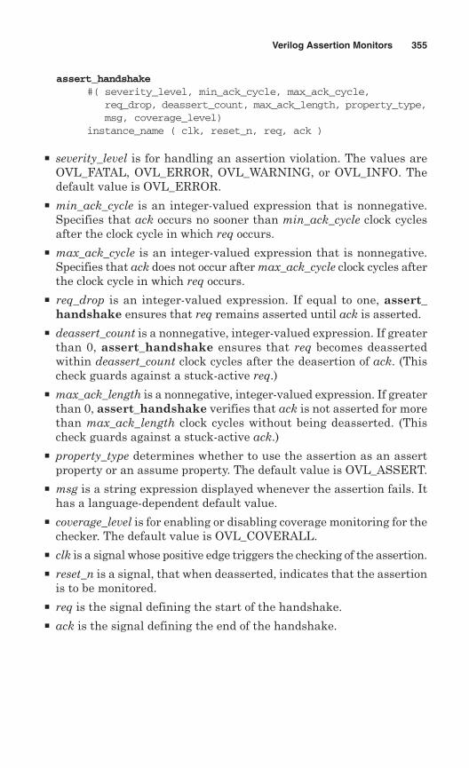
assert_handshake#( severity_level, min_ack_cycle, max_ack_cycle,
req_drop, deassert_count, max_ack_length, property_type, msg, coverage_level)
instance_name ( clk, reset_n, req, ack )
� severity_level is for handling an assertion violation. The values areOVL_FATAL, OVL_ERROR, OVL_WARNING, or OVL_INFO. Thedefault value is OVL_ERROR.
� min_ack_cycle is an integer-valued expression that is nonnegative.Specifies that ack occurs no sooner than min_ack_cycle clock cyclesafter the clock cycle in which req occurs.
� max_ack_cycle is an integer-valued expression that is nonnegative.Specifies that ack does not occur after max_ack_cycle clock cycles afterthe clock cycle in which req occurs.
� req_drop is an integer-valued expression. If equal to one, assert_handshake ensures that req remains asserted until ack is asserted.
� deassert_count is a nonnegative, integer-valued expression. If greaterthan 0, assert_handshake ensures that req becomes deassertedwithin deassert_count clock cycles after the deasertion of ack. (Thischeck guards against a stuck-active req.)
� max_ack_length is a nonnegative, integer-valued expression. If greaterthan 0, assert_handshake verifies that ack is not asserted for morethan max_ack_length clock cycles without being deasserted. (Thischeck guards against a stuck-active ack.)
� property_type determines whether to use the assertion as an assertproperty or an assume property. The default value is OVL_ASSERT.
� msg is a string expression displayed whenever the assertion fails. Ithas a language-dependent default value.
� coverage_level is for enabling or disabling coverage monitoring for thechecker. The default value is OVL_COVERALL.
� clk is a signal whose positive edge triggers the checking of the assertion.� reset_n is a signal, that when deasserted, indicates that the assertion
is to be monitored.� req is the signal defining the start of the handshake.� ack is the signal defining the end of the handshake.
Verilog Assertion Monitors 355
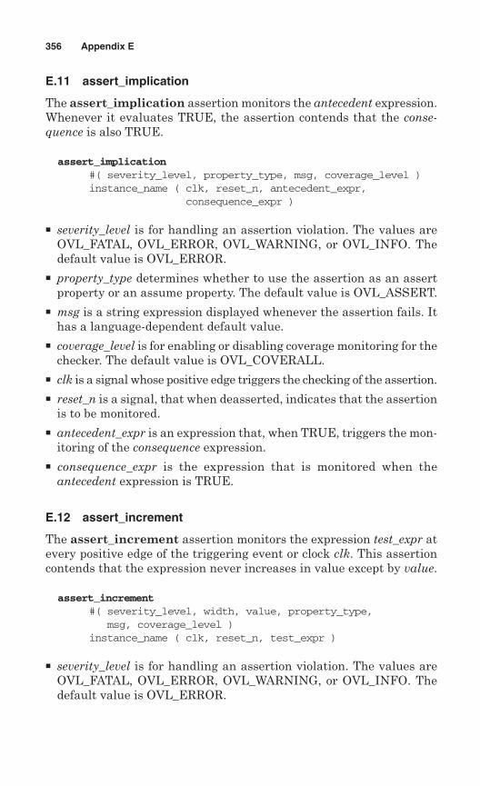
E.11 assert_implication
The assert_implication assertion monitors the antecedent expression.Whenever it evaluates TRUE, the assertion contends that the conse-quence is also TRUE.
assert_implication#( severity_level, property_type, msg, coverage_level )instance_name ( clk, reset_n, antecedent_expr,
consequence_expr )
� severity_level is for handling an assertion violation. The values areOVL_FATAL, OVL_ERROR, OVL_WARNING, or OVL_INFO. Thedefault value is OVL_ERROR.
� property_type determines whether to use the assertion as an assertproperty or an assume property. The default value is OVL_ASSERT.
� msg is a string expression displayed whenever the assertion fails. Ithas a language-dependent default value.
� coverage_level is for enabling or disabling coverage monitoring for thechecker. The default value is OVL_COVERALL.
� clk is a signal whose positive edge triggers the checking of the assertion.� reset_n is a signal, that when deasserted, indicates that the assertion
is to be monitored.� antecedent_expr is an expression that, when TRUE, triggers the mon-
itoring of the consequence expression.� consequence_expr is the expression that is monitored when the
antecedent expression is TRUE.
E.12 assert_increment
The assert_increment assertion monitors the expression test_expr atevery positive edge of the triggering event or clock clk. This assertioncontends that the expression never increases in value except by value.
assert_increment#( severity_level, width, value, property_type,
msg, coverage_level ) instance_name ( clk, reset_n, test_expr )
� severity_level is for handling an assertion violation. The values areOVL_FATAL, OVL_ERROR, OVL_WARNING, or OVL_INFO. Thedefault value is OVL_ERROR.
356 Appendix E
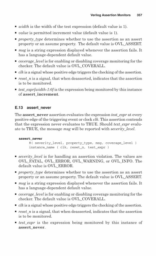
� width is the width of the test expression (default value is 1).� value is permitted increment value (default value is 1).� property_type determines whether to use the assertion as an assert
property or an assume property. The default value is OVL_ASSERT.� msg is a string expression displayed whenever the assertion fails. It
has a language-dependent default value.� coverage_level is for enabling or disabling coverage monitoring for the
checker. The default value is OVL_COVERALL.� clk is a signal whose positive edge triggers the checking of the assertion.� reset_n is a signal, that when deasserted, indicates that the assertion
is to be monitored.� test_expr[width-1:0] is the expression being monitored by this instance
of assert_increment.
E.13 assert_never
The assert_never assertion evaluates the expression test_expr at everypositive edge of the triggering event or clock clk. This assertion contendsthat the expression never evaluates to TRUE. Should text_expr evalu-ate to TRUE, the message msg will be reported with severity_level.
assert_never#( severity_level, property_type, msg, coverage_level ) instance_name ( clk, reset_n, test_expr )
� severity_level is for handling an assertion violation. The values areOVL_FATAL, OVL_ERROR, OVL_WARNING, or OVL_INFO. Thedefault value is OVL_ERROR.
� property_type determines whether to use the assertion as an assertproperty or an assume property. The default value is OVL_ASSERT.
� msg is a string expression displayed whenever the assertion fails. Ithas a language-dependent default value.
� coverage_level is for enabling or disabling coverage monitoring for thechecker. The default value is OVL_COVERALL.
� clk is a signal whose positive edge triggers the checking of the assertion.� reset_n is a signal, that when deasserted, indicates that the assertion
is to be monitored.� test_expr is the expression being monitored by this instance of
assert_never.
Verilog Assertion Monitors 357
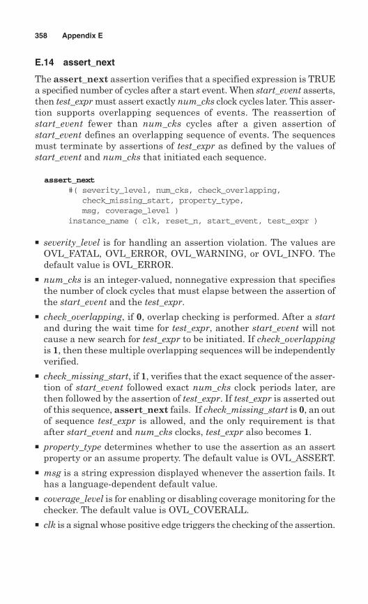
E.14 assert_next
The assert_next assertion verifies that a specified expression is TRUEa specified number of cycles after a start event. When start_event asserts,then test_expr must assert exactly num_cks clock cycles later. This asser-tion supports overlapping sequences of events. The reassertion ofstart_event fewer than num_cks cycles after a given assertion ofstart_event defines an overlapping sequence of events. The sequencesmust terminate by assertions of test_expr as defined by the values ofstart_event and num_cks that initiated each sequence.
assert_next#( severity_level, num_cks, check_overlapping,
check_missing_start, property_type, msg, coverage_level )
instance_name ( clk, reset_n, start_event, test_expr )
� severity_level is for handling an assertion violation. The values areOVL_FATAL, OVL_ERROR, OVL_WARNING, or OVL_INFO. Thedefault value is OVL_ERROR.
� num_cks is an integer-valued, nonnegative expression that specifiesthe number of clock cycles that must elapse between the assertion ofthe start_event and the test_expr.
� check_overlapping, if 0, overlap checking is performed. After a startand during the wait time for test_expr, another start_event will notcause a new search for test_expr to be initiated. If check_overlappingis 1, then these multiple overlapping sequences will be independentlyverified.
� check_missing_start, if 1, verifies that the exact sequence of the asser-tion of start_event followed exact num_cks clock periods later, arethen followed by the assertion of test_expr. If test_expr is asserted outof this sequence, assert_next fails. If check_missing_start is 0, an outof sequence test_expr is allowed, and the only requirement is thatafter start_event and num_cks clocks, test_expr also becomes 1.
� property_type determines whether to use the assertion as an assertproperty or an assume property. The default value is OVL_ASSERT.
� msg is a string expression displayed whenever the assertion fails. Ithas a language-dependent default value.
� coverage_level is for enabling or disabling coverage monitoring for thechecker. The default value is OVL_COVERALL.
� clk is a signal whose positive edge triggers the checking of the assertion.
358 Appendix E
� reset_n is a signal, that when deasserted, indicates that the assertionis to be monitored.
� start_event is the expression whose assertion defines the start of theevent sequence.
� test_expr is the expression whose assertion defines the end of theevent sequence.
E.15 assert_no_overflow
The assert_no_overflow assertion evaluates the expression test_exprat every positive edge of the triggering event or clock clk. This assertioncontends that the expression never takes on a value outside of the rangemin to max, inclusive.
assert_no_overflow #( severity_level, width, min, max, property_type,
msg, coverage_level ) instance_name ( clk, reset_n, test_expr )
� severity_level is for handling an assertion violation. The values areOVL_FATAL, OVL_ERROR, OVL_WARNING, or OVL_INFO. Thedefault value is OVL_ERROR.
� width is an integer-valued, nonnegative expression describing thewidth of test_expr. Implementations are allowed, but not required torestrict the maximum value of width.
� min The permissible minimum value of test_expr. The default valueis 0.
� property_type determines whether to use the assertion as an assertproperty or an assume property. The default value is OVL_ASSERT.
� max The permissible maximum value of test_expr.� msg is a string expression displayed whenever the assertion fails. It
has a language-dependent default value.� coverage_level is for enabling or disabling coverage monitoring for the
checker. The default value is OVL_COVERALL.� clk is a signal whose positive edge triggers the checking of the assertion.� reset_n is a signal, that when deasserted, indicates that the assertion
is to be monitored.� test_expr[width-1:0] the expression being monitored by this instance
of assert_no_overflow.
Verilog Assertion Monitors 359
E.16 assert_no_transition
The assert_no_transition assertion checks the expression test_expr atevery positive edge of the triggering event or clock clk. When the valueof text_expr is equal to start_state (i.e., the machine is in the start state)this assertion contends that test_expr never transits to the value ofnext_state (i.e., the machine stays in the start state). The width param-eter defines the size of test_expr.
assert_no_transition#( severity_level, width, property_type, msg, coverage_level )
instance_name ( clk, reset_n, test_expr, start_state, next_state )
� severity_level is for handling an assertion violation. The values areOVL_FATAL, OVL_ERROR, OVL_WARNING, or OVL_INFO. Thedefault value is OVL_ERROR.
� width is an integer-valued, nonnegative expression describing thewidth of test_expr. The default value is 1.
� property_type determines whether to use the assertion as an assertproperty or an assume property. The default value is OVL_ASSERT.
� msg is a string expression displayed whenever the assertion fails. Ithas a language-dependent default value.
� coverage_level is for enabling or disabling coverage monitoring for thechecker. The default value is OVL_COVERALL.
� clk is a signal whose positive edge triggers the checking of theassertion.
� reset_n is a signal, that when deasserted, indicates that the assertionis to be monitored.
� test_expr[width-1:0] is the expression being monitored by this instanceof assert_no_transition.
� start_state[width-1:0] is the value of test_expr that triggers the assertion.� next_state[width-1:0] is the value of test_expr being guarded against.
E.17 assert_no_underflow
The assert_no_underflow assertion evaluates the expression test_exprat every positive edge of the triggering event or clock clk. This assertioncontends that the expression never takes on a value outside of the rangemin to max, exclusive.
360 Appendix E
assert_no_underflow#( severity_level, width, min, max, property_type,
msg, coverage_level )instance_name ( clk, reset_n, test_expr )
� severity_level is for handling an assertion violation. The values areOVL_FATAL, OVL_ERROR, OVL_WARNING, or OVL_INFO. Thedefault value is OVL_ERROR.
� width is an integer-valued, nonnegative expression describing thewidth of test_expr. Implementations are allowed, but not required torestrict the maximum value of width.
� min is the permissible minimum value of test_expr. The default valueis 0.
� max is the permissible maximum value of test_expr. � property_type determines whether to use the assertion as an assert
property or an assume property. The default value is OVL_ASSERT.� msg is a string expression displayed whenever the assertion fails. It
has a language-dependent default value.� coverage_level is for enabling or disabling coverage monitoring for the
checker. The default value is OVL_COVERALL.� clk is a signal whose positive edge triggers the checking of the assertion.� reset_n is a signal, that when deasserted, indicates that the assertion
is to be monitored.� test_expr[width-1:0] is the expression being monitored by this instance
of assert_no_underflow.
E.18 assert_odd_parity
The assert_odd_parity assertion monitors the expression test_expr atevery positive edge of the triggering event or clock clk. This assertioncontends that the expression always has an odd number of bits asserted.
assert_odd_parity#( severity_level, width, property_type, msg, coverage_level )instance_name ( clk, reset_n, test_expr )
� severity_level is for handling an assertion violation. The values areOVL_FATAL, OVL_ERROR, OVL_WARNING, or OVL_INFO. Thedefault value is OVL_ERROR.
� width is the width of the test expression (default value is 1).
Verilog Assertion Monitors 361
� property_type determines whether to use the assertion as an assertproperty or an assume property. The default value is OVL_ASSERT.
� msg is a string expression displayed whenever the assertion fails. Ithas a language-dependent default value.
� coverage_level is for enabling or disabling coverage monitoring for thechecker. The default value is OVL_COVERALL.
� clk is a signal whose positive edge triggers the checking of the assertion.� reset_n is a signal, that when deasserted, indicates that the assertion
is to be monitored.� test_expr[width-1:0] is the expression being monitored by this instance
of assert_odd_parity.
E.19 assert_one_cold
The assert_one_cold assertion monitors the expression test_expr atevery positive edge of the triggering event or clock clk. This assertioncontends that the expression always has either exactly one bitdeasserted or has the appropriate inactive state (either all zero bits orall one bits), depending on the value of the inactive parameter.
assert_one_cold#( severity_level, width, inactive, property_type,
msg, coverage_level )instance_name ( clk, reset_n, test_expr )
� severity_level is for handling an assertion violation. The values areOVL_FATAL, OVL_ERROR, OVL_WARNING, or OVL_INFO. Thedefault value is OVL_ERROR.
� width is the width of the test expression (default value is 1).� inactive specifies the inactive state of test_expr. It has three possible
values:� `OVL_ALL_ZEROS, allows an all-zero value of test_expr without the
generation of a report.� `OVL_ALL_ONES, allows an all-one value of test_expr without the
generation of a report.� `OVL_ONE_COLD (default) allows no inactive state. At all times,
test_expr must have exactly one bit deasserted.� property_type determines whether to use the assertion as an assert
property or an assume property. The default value is OVL_ASSERT.
362 Appendix E
� msg is a string expression displayed whenever the assertion fails. Ithas a language-dependent default value.
� coverage_level is for enabling or disabling coverage monitoring for thechecker. The default value is OVL_COVERALL.
� clk is a signal whose positive edge triggers the checking of the assertion.� reset_n is a signal, that when deasserted, indicates that the assertion
is to be monitored.� test_expr[width-1:0] is the expression being monitored by this instance
of assert_one_cold.
E.20 assert_one_hot
The assert_one_hot assertion monitors the expression test_expr atevery positive edge of the triggering event or clock clk. This assertioncontends that the expression always has exactly one bit asserted.
assert_one_hot#( severity_level, width, property_type, msg, coverage_level )instance_name ( clk, reset_n, test_expr )
� severity_level is for handling an assertion violation. The values areOVL_FATAL, OVL_ERROR, OVL_WARNING, or OVL_INFO. Thedefault value is OVL_ERROR.
� width is the width of the test expression (default value is 1).� property_type determines whether to use the assertion as an assert
property or an assume property. The default value is OVL_ASSERT.� msg is a string expression displayed whenever the assertion fails. It
has a language-dependent default value.� coverage_level is for enabling or disabling coverage monitoring for the
checker. The default value is OVL_COVERALL.� clk is a signal whose positive edge triggers the checking of the assertion.� reset_n is a signal, that when deasserted, indicates that the assertion
is to be monitored.� test_expr[width-1:0] is the expression being monitored by this instance
of assert_one_hot.
E.21 assert_proposition
The assert_proposition assertion continually monitors the expres-sion test_expr; unlike assert_always, test_expr is not sampled by aclock. This assertion contends that the expression always evaluates to
Verilog Assertion Monitors 363
TRUE. Should the expression evaluate to FALSE, the message msg willbe reported with severity_level.
assert_proposition#( severity_level, property_type, msg, coverage_level ) instance_name ( reset_n, test_expr )
� severity_level is for handling an assertion violation. The values areOVL_FATAL, OVL_ERROR, OVL_WARNING, or OVL_INFO. Thedefault value is OVL_ERROR.
� property_type determines whether to use the assertion as an assertproperty or an assume property. The default value is OVL_ASSERT.
� msg is a string expression displayed whenever the assertion fails. Ithas a language-dependent default value.
� coverage_level is for enabling or disabling coverage monitoring for thechecker. The default value is OVL_COVERALL.
� reset_n is a signal, that when deasserted, indicates that the assertionis to be monitored.
� test_expr the expression being monitored by this instance ofassert_proposition.
E.22 assert_quiescent_state
The assert_quiescent_state assertion continually monitors the sampleevent on every rising edge of clk. This assertion contends that state_expris equal to check_value whenever sample_event is asserted, and option-ally when the entire system is quiescent.
assert_quiescent_state#( severity_level, width, property_type, msg, coverage_level )instance_name ( clk, reset_n, state_expr, check_value,
sample_event )
� severity_level is for handling an assertion violation. The values areOVL_FATAL, OVL_ERROR, OVL_WARNING, or OVL_INFO. Thedefault value is OVL_ERROR.
� width is the width of the test expression (default value is 1).� property_type determines whether to use the assertion as an assert
property or an assume property. The default value is OVL_ASSERT.� msg is a string expression displayed whenever the assertion fails. It
has a language-dependent default value.
364 Appendix E
� coverage_level is for enabling or disabling coverage monitoring for thechecker. The default value is OVL_COVERALL.
� clk is a signal whose positive edge triggers the checking of the assertion.� reset_n is a signal, that when deasserted, indicates that the assertion
is to be monitored.� state_expr[width-1:0] is the expression being monitored by this
instance of assert_quiescent_state.� check_value[width-1:0] is the value of state_expr that indicates qui-
escence.� sample_event when TRUE, causes the assertion to check state_expr.
E.23 assert_range
The assert_range assertion evaluates the expression test_expr at everypositive edge of the triggering event or clock clk. This assertion contendsthat the expression never takes on a value outside of the range min tomax, inclusive.
assert_range#( severity_level, width, min, max, property_type,
msg, coverage_level )instance_name ( clk, reset_n, test_expr )
� severity_level is for handling an assertion violation. The values areOVL_FATAL, OVL_ERROR, OVL_WARNING, or OVL_INFO. Thedefault value is OVL_ERROR.
� width is an integer-valued, nonnegative expression describing thewidth of test_expr.
� min is the permissible minimum value of test_expr. The default valueis 0.
� max is the permissible maximum value of test_expr. The default valueis 2**width – 1. max must be greater than or equal to min.
� property_type determines whether to use the assertion as an assertproperty or an assume property. The default value is OVL_ASSERT.
� msg is a string expression displayed whenever the assertion fails. Ithas a language-dependent default value.
� coverage_level is for enabling or disabling coverage monitoring for thechecker. The default value is OVL_COVERALL.
� clk is a signal whose positive edge triggers the checking of the assertion.
Verilog Assertion Monitors 365
� reset_n is a signal, that when deasserted, indicates that the assertionis to be monitored.
� test_expr[width-1:0] is the expression being monitored by this instanceof assert_range.
E.24 assert_time
The assert_time assertion continually evaluates the expressiontest_expr. This assertion contends that the expression remains TRUEfor at least a specified number of clock periods.
assert_time#( severity_level, num_cks, action_on_new_start,
property_type, msg, coverage_level )instance_name ( clk, reset_n, start_event, test_expr )
� severity_level is for handling an assertion violation. The values areOVL_FATAL, OVL_ERROR, OVL_WARNING, or OVL_INFO. Thedefault value is OVL_ERROR.
� num_cks specifies the minimum number of clock cycles that test_exprmust hold each time it asserts.
� action_on_new_start is the method of handling a new start that occursbefore test_expr changes value or num_cks cycles transpire without achange.� `OVL_IGNORE_NEW_START (default), ignores all assertions of
start_event after the first assertion has been detected.� `OVL_RESET_ON_NEW_START, restart monitoring of test_expr if
start_event is asserted in any subsequent clock assertion duringthe monitoring of test_expr.
� `OVL_ERROR_ON_NEW_START, while monitoring, issue an errorif start_event is asserted in any clock cycle subsequent to the cyclein which monitoring began.
� property_type determines whether to use the assertion as an assertproperty or an assume property. The default value is OVL_ASSERT.
� msg is a string expression displayed whenever the assertion fails. Ithas a language-dependent default value.
� coverage_level is for enabling or disabling coverage monitoring for thechecker. The default value is OVL_COVERALL.
� clk is a signal whose positive edge triggers the checking of the assertion.
366 Appendix E
� reset_n is a signal, that when deasserted, indicates that the assertionis to be monitored.
� start_event is the event that, when asserted, triggers the monitoringof test_expr.
� test_expr is the expression being monitored by this instance ofassert_time.
E.25 assert_transition
The assert_transition assertion monitors the expression test_expr atevery positive edge of the triggering event or clock clk. When the valueof test_expr is equal to start_state this assertion contends that, if test_exprchanges value, it will change to the value of end_state. The width param-eter defines the size of test_expr.
assert_transition#( severity_level, width, property_type, msg, coverage_level )instance_name ( clk, reset_n, test_expr, start_state,
next_state )
� severity_level is for handling an assertion violation. The values areOVL_FATAL, OVL_ERROR, OVL_WARNING, or OVL_INFO. Thedefault value is OVL_ERROR.
� width is an integer-valued, nonnegative expression describing thewidth of test_expr. The default value is 1.
� property_type determines whether to use the assertion as an assertproperty or an assume property. The default value is OVL_ASSERT.
� msg is a string expression displayed whenever the assertion fails. Ithas a language-dependent default value.
� coverage_level is for enabling or disabling coverage monitoring for thechecker. The default value is OVL_COVERALL.
� clk is a signal whose positive edge triggers the checking of the assertion.� reset_n is a signal, that when deasserted, indicates that the assertion
is to be monitored.� test_expr[width-1:0] is the expression being monitored by this instance
of assert_transition.� start_state[width-1:0] is the value of test_expr that triggers the assertion.� next_state[width-1:0] is the value that test_expr should assume in the
next clock cycle.
Verilog Assertion Monitors 367
E.26 assert_unchange
The assert_unchange assertion evaluates the expression test_expr atevery positive edge of the triggering event or clock clk. This assertioncontends that, when triggered, test_expr remains stable for at least aspecified number of clock periods.
assert_unchange#( severity_level, num_cks, action_on_new_start,
property_type, msg, coverage_level ) instance_name ( clk, reset_n, start_event, test_expr )
� severity_level is for handling an assertion violation. The values areOVL_FATAL, OVL_ERROR, OVL_WARNING, or OVL_INFO. Thedefault value is OVL_ERROR.
� num_cks specifies the minimum number of clock cycles that test_exprmust remain unchanged each time start_event is asserted.
� action_on_new_start is the method of handling a new start that occursbefore test_expr changes value or num_cks cycles transpire without achange.� `OVL_IGNORE_NEW_START (default), ignores all assertions of
start_event after the first assertion has been detected.� `OVL_RESET_ON_NEW_START, restart monitoring of test_expr if
start_event is asserted in any subsequent clock assertion duringthe monitoring of test_expr.
� `OVL_ERROR_ON_NEW_START, while monitoring, issue an errorif start_event is asserted in any clock cycle subsequent to the cyclein which monitoring began.
� property_type determines whether to use the assertion as an assertproperty or an assume property. The default value is OVL_ASSERT.
� msg is a string expression displayed whenever the assertion fails. Ithas a language-dependent default value.
� coverage_level is for enabling or disabling coverage monitoring for thechecker. The default value is OVL_COVERALL.
� clk is a signal whose positive edge triggers the checking of the assertion.� reset_n is a signal, that when deasserted, indicates that the assertion
is to be monitored.� start_event is the event that, when asserted, triggers the monitoring
of test_expr.� test_expr[width-1:0] is the expression being monitored by this instance
of assert_unchange.
368 Appendix E
E.27 assert_width
The assert_width assertion continually evaluates the expressiontest_expr. This assertion contends that the expression remains TRUEfor at least a specified minimum number of clock periods and no longerthan a specified maximum number of clock periods.
assert_width#( severity_level, min_cks, max_cks, property_type,
msg, coverage_level ) instance_name ( clk, reset_n, test_expr )
� severity_level is for handling an assertion violation. The values areOVL_FATAL, OVL_ERROR, OVL_WARNING, or OVL_INFO. Thedefault value is OVL_ERROR.
� min_cks specifies the minimum number of clock cycles that test_exprmust hold each time it asserts. If 0, there is no minimum number ofclocks; test_expr may be asserted at start_event.
� max_cks specifies the maximum number of clock cycles that test_exprmust hold each time it asserts. If 0, there is no maximum check;test_expr may deassert at any time after it asserts.
� property_type determines whether to use the assertion as an assertproperty or an assume property. The default value is OVL_ASSERT.
� msg is a string expression displayed whenever the assertion fails. Ithas a language-dependent default value.
� coverage_level is for enabling or disabling coverage monitoring for thechecker. The default value is OVL_COVERALL.
� clk is a signal whose positive edge triggers the checking of the assertion.� reset_n is a signal, that when deasserted, indicates that the assertion
is to be monitored.� start_event is the event that, when asserted, triggers the monitoring
of test_expr.� test_expr is the expression being monitored by this instance of
assert_width.
E.28 assert_win_change
The assert_win_change assertion continually monitors start_event atevery positive edge of the triggering event or clock clk. When start_eventis asserted, this assertion monitors the expression test_expr to assure
Verilog Assertion Monitors 369
that it changes value prior to the assertion of the end_event. Whenstart_event asserts, this assertion verifies that the test_expr changesvalue on a clock edge that occurs before or coincident with the nextassertion of end_event. Once test_expr changes value, it need not remainstable until end_event asserts.
assert_win_change#( severity_level, width, property_type, msg, coverage_level )instance_name ( clk, reset_n, start_event, test_expr,
end_event )
� severity_level is for handling an assertion violation. The values areOVL_FATAL, OVL_ERROR, OVL_WARNING, or OVL_INFO. Thedefault value is OVL_ERROR.
� width is an integer-valued, nonnegative expression describing thewidth of test_expr. The default value is 1.
� property_type determines whether to use the assertion as an assertproperty or an assume property. The default value is OVL_ASSERT.
� msg is a string expression displayed whenever the assertion fails. Ithas a language-dependent default value.
� coverage_level is for enabling or disabling coverage monitoring for thechecker. The default value is OVL_COVERALL.
� clk is a signal whose positive edge triggers the checking of the assertion.� reset_n is a signal, that when deasserted, indicates that the assertion
is to be monitored.� start_event is the event that, when asserted, triggers the monitoring
of test_expr.� test_expr[width-1:0] is the expression being monitored by this instance
of assert_win_change.� end_event is the event that, when asserted, terminates the monitor-
ing of test_expr.
E.29 assert_win_unchange
The assert_win_unchange assertion continually monitors start_eventat every positive edge of the triggering event or clock clk. Whenstart_event is asserted, this assertion monitors the expression test_exprto assure that it does not change value prior to the assertion ofend_event.
370 Appendix E
assert_win_unchange#( severity_level, width, property_type, msg, coverage_level )instance_name ( clk, reset_n, start_event, test_expr,
end_event )
� severity_level is for handling an assertion violation. The values areOVL_FATAL, OVL_ERROR, OVL_WARNING, or OVL_INFO. Thedefault value is OVL_ERROR.
� width is an integer-valued, nonnegative expression describing thewidth of test_expr. The default value is 1.
� property_type determines whether to use the assertion as an assertproperty or an assume property. The default value is OVL_ASSERT.
� msg is a string expression displayed whenever the assertion fails. Ithas a language-dependent default value.
� coverage_level is for enabling or disabling coverage monitoring for thechecker. The default value is OVL_COVERALL.
� clk is a signal whose positive edge triggers the checking of theassertion.
� reset_n is a signal, that when deasserted, indicates that the assertionis to be monitored.
� start_event is the event that, when asserted, triggers the monitoringof test_expr.
� test_expr[width-1:0] is the expression being monitored by this instanceof assert_win_unchange.
� end_event is the event that, when asserted, terminates the monitor-ing of test_expr.
E.30 assert_window
The assert_window assertion continually monitors the start_event atevery positive edge of the triggering event or clock clk. When start_eventis asserted, this assertion contends that the expression test_expr remainsTRUE at every subsequent positive clock edge until the assertion of theend_event.
assert_window#( severity_level, property_type, msg, coverage_level ) instance_name ( clk, reset_n, start_event, test_expr,
end_event )
Verilog Assertion Monitors 371
� severity_level is for handling an assertion violation. The values areOVL_FATAL, OVL_ERROR, OVL_WARNING, or OVL_INFO. Thedefault value is OVL_ERROR.
� property_type determines whether to use the assertion as an assertproperty or an assume property. The default value is OVL_ASSERT.
� msg is a string expression displayed whenever the assertion fails. Ithas a language-dependent default value.
� coverage_level is for enabling or disabling coverage monitoring for thechecker. The default value is OVL_COVERALL.
� clk is a signal whose positive edge triggers the checking of theassertion.
� reset_n is a signal, that when deasserted, indicates that the assertionis to be monitored.
� start_event is the event that, when asserted, triggers the monitoringof test_expr.
� test_expr is the expression being monitored by this instance ofassert_window.
� end_event is the event that, when asserted, terminates the monitor-ing of test_expr.
E.31 assert_zero_one_hot
The assert_zero_one_hot assertion checker checks the expressiontest_expr at every positive edge of the triggering event or clock clk. Thisassertion contends that the expression always has at most one bitasserted.
assert_zero_one_hot#( severity_level, width, property_type, msg, coverage_level )instance_name ( clk, reset_n, test_expr )
� severity_level is for handling an assertion violation. The values areOVL_FATAL, OVL_ERROR, OVL_WARNING, or OVL_INFO. Thedefault value is OVL_ERROR.
� width is the width of the test expression (default value is 1).� property_type determines whether to use the assertion as an assert
property or an assume property. The default value is OVL_ASSERT.� msg is a string expression displayed whenever the assertion fails. It
has a language-dependent default value.
372 Appendix E
� coverage_level is for enabling or disabling coverage monitoring for thechecker. The default value is OVL_COVERALL.
� clk is a signal whose positive edge triggers the checking of the assertion.� reset_n is a signal, that when deasserted, indicates that the assertion
is to be monitored.� test_expr[width-1:0] is the expression being monitored by this instance
of assert_zero_one_hot.
Verilog Assertion Monitors 373

This page intentionally left blank
Index
375
# sign, 24, 38$array, 156$async$nand$array, 75, 156$asynch, 156$bitstoreal, 75$display, 33, 34, 44, 67–68, 73, 201,
203–204$displayb, 45, 200$fflush, 278, 280$fgetc, 73$fgets, 279, 280$finish, 74, 84, 85, 106, 193, 197,
198, 205, $fopen, 73, 277, 280, 303, 304$fread, 73$frewind, 73$fscanf, 73, 278–280$fseek, 73, 278–280$hold, 150$itor, 75$monitor, 73, 200, 201, 248, 249$nand, 156$nochange, 74$period, 150$printtimescale, 74$random, 76, 198, 204, 205$readmemb, 153, 156, 181$readmemh, 73, 153–155, 187,
263, 302–304$realtime, 76$realtobits, 75$rtoi, 75$scanf, 73$setup, 44, 149–150
$setuphold, 150$sformat, 302–304$sign, 73$sscanf, 73$stime, 76$stop, 6, 41, 74, 197, 202–206, 249,
263, 277, 301$strobe, 203, 204$swrite, 73$sync_async$and_or$array_plane,
74$time, 33, 67, 76, 200, 201, 249$time, 57$timeformat, 74$timescale, 22, 23, 44, 74$width, 150%b, 200 %t, 200%v, 248@ sign, 27`define, 172`celldefine, 72`celldefine, 72`default–nettype, 71`default–nettype, 71`define, 71–72, 175`else, 72`endcelldefine, 72`endif, 72`ifdef, 72`include, 71, 110`nounconnected_drive, 72`resetall, 71, 72`timescale, 71, 92
Copyright © 2006 by The McGraw-Hill Publishing Companies, Inc. Click here for terms of use.
`unconnected_drive, 72`undef, 72
2-to-1 Multiplexer, 230, 231, 2504-bit Adder, 95, 96, 4-bit Comparator, 107, 108, 1334-bit Shifter, 2324-value logic, See four-value logic
abstraction level, 11, 15, 102Accellera, 208add operation, 109add-and-shift, 253, 255address range, 46Altera, 10, 184ALU, 27–28, 121, 124, 125, 130,
132, 192, 269, 281, 285, 286always, 65always block, 26, 27, 30, 31, 34, 68,
113, 114, 116, 118, 129, 130 always statement, 21, 24–25, 34,
113, 117, 129, 139ambiguity, 48ambiguous conditions, 105ambiguous strength, 250ambiguous value, 105, 106, 173, 176analysis, 7and primitive, 82, 87and-or, 74antecedent, 217AOI, 229–230application-specific integrated
circuits, See ASICarithmetic, 48arithmetic expressions, 108, 119arithmetic logic unit, See ALUarithmetic operators, 48, 108, 162arithmetic shift, 51array, 46, 153array declaration, 46, 47array indexing, 58array indexing, 58, 96array of instances, 96, 97array_plane, 74ASIC, 2, 3, 7, 9, 10, 223assert_one_hot, 212, 213assert_always, 208–210, 220assert_always_on_edge, 208
assert_change, 208, 211assert_cycle_sequence, 208, 213,
214, 216assert_decrement, 208assert_delta, 208assert_even_parity, 208assert_fifo_index, 208assert_frame, 208assert_handshake, 208assert_implication, 208, 217, 219assert_increment, 208assert_never, 208assert_never_at_x_or_z, 208assert_next, 208, 215–218assert_no_overflow, 208, 218–220assert_no_transition, 208assert_no_underflow, 208assert_odd_parity, 208assert_one_cold, 208assert_one_hot, 208, 211–213assert_proposition, 208assert_quiescent_state, 208assert_range, 208assert_time, 208assert_transition, 208assert_unchange, 208assert_width, 208assert_win_change, 208assert_win_unchange, 208assert_window, 208assert_zero_one_hot, 208assertion, 6, 138assertion library, 207assertion module, 207, 209assertion monitor, 6, 207–210, 298assertion templates, 216assertion verification, 3, 4, 6, 191,
207, 208, assign statement, 20, 22, 23, 25,
38, 39–40, 102–105, 109–114,128, 132
assign-deassign, 148asynchronous, 74, 157, 180, 217asynchronous circuit, 30asynchronous clear, 185asynchronous control, 146asynchronous data signal, 30asynchronous PLA, 75
376 Index
asynchronous preset, 185asynchronous reset, 149asynchronous set, 145, 149asynchronous set and reset, 144, 145,
149, 153, 164, 187, 188, 217auxiliary logic, 213
barrel shifter, 233, 234 base specification, 45based numbers, 57base-identifier, 45basic operators, 48BCD, 133, 209BCD counter, 210begin, 25begin-end bracketing, 115, 116, 118behavioral level, 12, 19, 112,144behavioral description, 31, 35, 113, 186behavioral model, 3, 142behavioral simulation, 5behavioral synthesis, 129behavioral Verilog, 2bidirectional, 12bidirectional, 153, 160, 225, 235, 239,
253, 259, 262bidirectional switches, 12, 225, 250bidirectionality, 154, 155binary, 44binary multiplication, 254binding, 8–9bit-select, 58–59bitwise operators, 50, 51, 102, 103blocking assignment, 24, 65–67,
78–79, 117blocking procedural assignments,
67, 110, 116, 130blocking procedural assignments, 110boolean operations, 48, 50bracketing, 114buf primitive, 86, 225, 244–245buffered data application, 205Bufif1, 83, 84, 86built-in gate, 242bus contention, 110bus resolution, 12bus specifications, 22bus structure, 110bussing, 129
CAD tools, 1Cadence Design Systems, 11capacitive, 42, 55capacitive model, 136capacitive net, 242, 250capacitive network, 243capacitive storage, 136capacitive wire, 55cascadable comparator, 107, 108cascading, 107case, 118, 120, 122, 125case alternative, 26, 32, 120, 122, 172case default, 130case equality operators, 49case expression, 120–122, 172, 273case inequality operators, 49case statement, 26–28, 31, 32, 120,
121, 125, 131, 160, 273, 279,288, 295
casex, 122casez, 121, 122charge, 241charge storage, 12charge strength, 242–243, 247clocked SR-latch, 138, 139, 140clocking, 171CMOS, 224, 225CMOS flip-flop, 56CMOS gates, 226, 227 CMOS NAND, 229code format, 41combinational, 181combinational block, 177combinational circuit, 81, 129combinational circuit testing, 192combinational UDP, 87, 139comments, 16, 41, 208comparator, 104, 107compare, 124, 125, 128compilation, 7compiler directives, 44, 71–72, 76complimentary metal oxide
semiconductor (CMOS), 12component description, 22concatenation, 157, 181concatenation operator, 26, 48, 52,
104, 122concurrency, 39, 40
Index 377
concurrent, 13, 26, 33, 39, 97concurrent assignments, 13, 129 concurrent body, 26, 39, 40, 61concurrent statements, 40, 43, 62,
97, 103, 178concurrent subcomponents, 39conditional assignment, 106conditional expression, 20, 155, 291conditional jump, 307conditional operation, 20, 105–106conditional operator, 52–53, 107conditional statements, 128conflict, 42conflict x, 232connection list, 94consequence, 217console, 34constant part-select, 58continuous assignments, 3, 43,
53, 56, 60, 61, 64, 65, 69, 70,128, 140
control/data partitioning, 16control part/unit, 16, 17controller, 29, 253, 256, 270, 287converting reals, 75counter, 24–25, 161 cross-couple SRAM memory, 237curly brackets, 26current state, 171custom IC, 2, 3, 7, 9, 10
data/control partitioning, 265data components, 22data files, 263data part, 16, 17data part/path, See datapathdata types, 37, 42, 54, 59, 60, 65,
70, 73, 76, Datapath, 16, 17, 253, 256–261,
265–276, 287deassign, 70, 148, 149decimal, 44default, 28, 120, 121, 160, 172,
176, 248default delay, 226default else, 145default net type, 82default strength, 238, 242defparam, 91
delay, 5, 12, 23–25, 38, 64, 66delay control, 66, 115, 116, 147delay control statement, 66, 115, 116 delay expression, 115delay formats, 88, 92, 100, 103delay parameters, 56, 61, 85–87, 100delay paths, 38delay specification, 61–62, 87, 88, 93,
99, 101, 116 delay3, 88design entry, 3design flow, 2design validation, 4design verification, 3, 206designer discipline, 208dirty page, 302display format specifications, 200display tasks, 73distribuited delay, 99–102 distributed delay, gate, 100DoD, 11Drain, 226drive, 241drive strength, 242–243D-type flip-flop, 144–150, 184,
187, 240,dynamic arguments, 209, 210dynamic cell, 239dynamic memory, 234dynamic RAM, 239
EDA, 1, 3, 11, 208EDA environments, 3electronic design automation,
See EDAElements of Verilog, 18else part, 123end keywords, 114endfunction, 109 endmodule, 18, 42endprimitive, 86endspecify, 99endtable, 88endtask, 277equality operator, 48–50, 107even control statement, 144, 146, 199event control, 65, 66, 113–115,
119, 199event driven simulation, 62
378 Index
event expression, 144event sequence, 216executable comments, 208external data files, 153, 220external files, 263external memory file, 162
fall delay, 88, 90, 91, 103 falling edge, 23, 211fault simulation, 11, 13, 19feedback model, 136feedback path, 237Fetch, 270, 293field programmable logic device,
See FPLDFIFO queue, 167file I/O, 276file I/O tasks, 73, 276file output, 73, 281finite state machine, 259flip-flop, 22–24, 42, 139, 150, 240flip-flop modeling, 144flow control, 113, 115for loop, 118, 123for procedural statement, 123 for statement, 98, 122, 123force, 70force and release, 70forcing 0, 42forcing 1, 42forever loop, 199fork-join, 146–147formal verification, 1, 3–4, 6, 13,
206–208four value logic, 12, 41, 62, 81, 241FPGA, 7FPLD, 3, 7, 9, 10full adder, 25, 39, 40, 57, 93, 94,
97–100, 104, 117, 118, 127, full adder tester, 41full-path, 100function, 34, 44, 72, 75, 109–110functional description, 78functional registers, 157functional specification, 7functional verification, 33, 127
Gate, 227gate capacitance, 234–235
gate delays, 5, 38gate level, 12, 127, 132, 234gate level delays, 111, 142gate level logic, 85gate level modeling, 223gate level primitives, 12, 137gate level simulation, 12gate level synthesis, 127gate level timing, 7gate output, 241gate primitives, 85, 86, 102, 133Gateway Design Automation, 11generate loops, 233generate statement, 96–98genvar, 98glitch, 38Gray code, 162, 213Gray code counter, 162, 163, 213
half-register, 235, 240hardware description languages
(HDL), 11, 18, 103, 223hardware generation, 10hardware modules, 18hardware/software environments, 73HDL, See hardware description
languageshexadecimal, 44hierarchical design, 13hierarchical fashion, 3hierarchical naming, 91, 139,
200, 202hierarchical structures, 93hierarchy, 13, 91, 93, 207high-impedance, 42, 153, 272, 302high-level synthesis, 1high-to-low propagation time (tphl),
25hold time, 150Huffman model, 176, 178–179,
187, 291identifier, 41, 43–44IEEE std 1364–1995, 11IEEE std 1364–2001, 41IEEE std 754–1985, 45if statement, 123if-condition, 120if-else, 21, 25, 31, 113, 118–119, 161immediate data, 266, 282
Index 379
implication, 217implicit model, 136inactive, 259inactive values, 130indexed part-select, 58indexing memories, 59infinite loop, 113, 147initial, 65initial block, 67–68initial reseting, 217initial statement, 34, 85, 122, 153,
183, 185, 192, 199, 200, 204initial value, 42, 56initializing reg, 197inout, 43, 81–82, 154inout ports, 225, 239input, 43, 81–82input/output specification, 23–24instance name, 29, 33instance name, 94, 96instantiation, 19–20instantiation statement, 4instantiation statements, 4instruction register, 281integer, 44, 45, 57interactive testbench, 201interconnections, 26, 28–29, 82intermediate format, 7intermediate signal values, 57intermediate wires, 20, 23intra-assignment delay, 66, 68, 116,
204, 116–117intra-assignment event, 116invalid state, 218iterative structure, 96
Join, See fork-join
large, 63latch, 137, See also SR-latchlevel (RTL), 3LFSR and MISR, 163limiting data sets, 198linear feedback shift register (LFSR),
163–166load, 157localparam, 90, 171–172, 176logic optimization, 8
logic value system, 41logical operation, 22, 27, 48, 50, 287logical shift, 51low to high propagation time (tplh),
25
majority circuit, 86, 90majority UDP, 88master-slave flip-flop, 141–142,
240–241maximum delay, 88Mealy machine, 174, 181, 217medium, 63memory, 59, 110, 153memory buffering, 276memory initialization, 153memory modeling, 276memory read, 266, 293min:typ:max, 88, 100, 103minimum delay, 88MISR, 164–164, 167–169missing delay values, 226mixbed synthesis, 132mnemonic, 266module, 18, 42, 81module instantiation, 21, 72, 85, 91,
94, 113, 124, 132, 209module name, 18module path delay, 99–100module ports, 43module with no ports, 196module-under-test, See MUTmodulus operation, 48monitoring, 73, 191monitors, 6Moore machine, 31, 171, 174,
176, 178 multidimensional arrays, 46–47multidimensional memories, 59, 137multiple assignments, 68–69multiple drivers, 64multiple input signature register, See
MISRmultiplexer, 19–22, 35, 82, 83, 105,
111, 118, 119, 132, 230–232, 254,257–259
multiply operation, 48MUT, 85, 191
380 Index
named connection, 29, 94named parameter assignment, 91nand primitive, 242n-bit adder, 97negative edge, 24, 25negedge, 23, 145nested condition operators, 106nested generate loops, 233nested if-then-else, 106, 120net, 42, 43, 55–56, 236net assignments, 63–64net declaration, 54, 56net declaration assignment, 63–64,
111, 242–243net strength, 242netlist, 10, 12nmos, 224–226, 232NMOS-PMOS inverter, 235nonblocking assignment, 24, 67–68,
117nonblocking procedural assignments,
67, 68, 116not, 83, 84number specification, 45numbers, 44–45
observability, 208, 220octal, 44octal latch, 157odd-even parity, 104opcode, 271Open Verification Library, See OVLoperations, 48operator precedence, 53operators, 13, 48 ordered connection, 29, 94ordered parameter assignment,
90–91, 94ordered port connection, 29output, 43, 81–82, 243output latch, 129output ports, 18 overdriving, 238overflow, 124, 132overriding parameters, 139OVI (Open Verilog International),
11OVL, 6, 11, 207–209, 220
parallel path, 101parameter, 90, 91, 111parameter declaration, 31parameter override, 91parameterized module instantiation,
91parameters, 18, 57, 91parity, 124–125part-select, 58pass gate logic, 230–231path delay, 100–102path delay specification, 99, 101, 102period check, 150pin-to-pin delay, 12, 93, 100PLA, 12, 74PLA modeling, 155PLA modeling tasks, 74–75PLD, 2PLI, 72pmos, 224, 232polynomial, 164ports, 18, 43, 81–82posedge, 144, 145positive-edge, 30postsynthesis, 10, 128postsynthesis simulation, 3, 10, 199precedence of operators, 53predefined bus resolution functions,
12predefined gate primitives, 85predefined parameters, 12predefined wire resolution functions,
12presynthesis description, 127presynthesis simulation, 4prime numbers, 194primitive instantiation, 19, 94primitives, 19, 82, 83, 85, 127procedural, 21, 24 procedural assignments, 65, 66, 115,
117, 131procedural assignments, 65–66,
130procedural block, 85, 113procedural block, 12, 13, 20, 40, 43,
112–118, 129, 137, procedural blocking assignments, 66procedural body, 40, 68
Index 381
procedural case statement, 120procedural continuous assignment,
65, 69–70procedural flow control, 65procedural for statement, 122procedural if-else, 118procedural statement, 3, 34, 110, 130procedural statement, 3procedural while loop, 123Program Counter, 281programmable logic arrays, 155programmable logic devices, See PLDProgramming Language Interface
(PLI), 13propagation delay, 85property, 6, 206–207property coverage, 7pseudo-static d-latch, 236pseudo-static memory, 234pull0, 63pull1, 63pulldown, 225pull-down, 228, 229, 231pull-up, 228, 231pulup, 225
Quartus II, 10queues, 167
random, 204random access, 12random data, 199random number generation, 163random time intervals, 204–205range specification, 46reading data files, 263real, 44, 45, 57realtime, 57reduction, 125reduction operation, 50–51, 105reduction XOR, 124reg, 25, 42, 54, 56–57, 113reg data type, 52, 54, 56, 66reg declaration, 56–57register, 26register block, 160register file, 187, 281, 285, 288register transfer, 3register transfer level, See RTL
registers, 22regular structure, 96, 97, 114 relational operation, 48, 105, 107release, 70repeat, 263repeat statement, 198, 202repetition multiplier, 52replication operation, 48, 52reset sequence, 216resistive 0, 1, 42resistive switches, 247resolution, 64, 243–244resolution function, 12, 224, 231,
244, 246response observation, 207retaining old values, 120, 121, 123,
129, 177rise delay, 88, 90, 91, 103rising clock edge, 30ROM based controller, 181routing and placement, 9RT level, See RTLRT level simulation, 4RTL, 3, 15, 16, 17, 253, 264–265RTL synthesis, 7
SAYEH, 281, 282SAYEH datapath, 283SAYEH Verilog description, 287seed, 163, 164, 167seed parameters, 165sensitive, 181sensitivity list, 26–27, 114, 129sequence detector, 30–31, 171,
188, 204sequential, 181sequential blocks, 160, 180sequential circuit, 70, 76, 135, 194sequential circuit synthesis, 186sequential circuit testing, 194, 218sequential multiplier, 253sequential UDP, 139–141 setup time, 149, 150seven-segment display, 133shadow instructions, 281shift operation, 51, 52, 157shift register, 26–27, 157shift-and-add, 254shifter, 26, 157, 232
382 Index
short instructions, 281signal strength, 223, 241signed, 54, 57signed data, 57signed number, 45simple architecture, yet enough
hardware, See SAYEHsimple assignments, 61simple procedural blocks, 113simple tester, 33, 84simulation, 3, 4simulation control, 197simulation control tasks, 74simulation performance, 229sizable register, 153size mismatches, 109size specification, 22sized integer, 44small, 63Source, 226, 227specify, 99specify block, 90, 100–101, 149–150 specify parameters, 90SRAM, 238SR-latch, 137, 138stacks, 167standard memory, 58state machine, 16, 31, 32, 171, 268state machine coding, 171 state machine testing, 195state transitions, 171static memory element, 237static parameters, 209Status Register, 281strength, 241, 243, 248strength modeling, 231, 241, 250strength reduction, 231, 247–248strength specification, 62–63strong, 238strong0, 63strong1, 63supply0, 56, 63, 227supply1, 56, 63, 227switch, 243switch level, 11, 13, 85, 127, 136,
228–230, 242, 250switch level 2-to-1 multiplexer, 231switch level barrel shifter, 234switch level half-register, 235
switch level memory element, 235switch level modeling, 11, 136, 223,
224, 241switch level primitives, 224, 225, 227switch level shifter, 232switch level timing, 11switch output, 241sync-async, 74synchronizer, 30synchronous, 176, 180, 217synchronous reset, 23, 24, 144synchronous reset, 160–161synchronous set, 144synthesis, 7– 9, 13, 19, 125, 127, 128,
131, 181, 261, 273synthesis tool, 11synthesizable, 183, 270synthesizable D-type flip-flop, 184synthesizable gate level, 128system functions, 75, 44, 72, 73system tasks, 12, 34, 44, 72, 73system tasks and functions, 72–76system utilities, 12, 75
target device, 3target hardware, 7, 9target library, 129, 183target technology, 127task, See system tasktest benches, 33–34testbench, 4–6, 33, 43, 72, 84, 106, 191,
192–207, 205, 262, 266, 276, 298testbench techniques, 195three-state, See tri-state timing, 4, 5, 7, 10, 13, 19, 34, 37–40,
64, 85, 135, 191, 223timing analysis, 2, 8, 10, 11timing and concurrency, 13, 37, 40, 76timing check tasks, 74 timing constructs, 11timing control, 67, 68, 113, 115, 143timing diagram, 5, 214, 232, 239timing parameters, 127timing simulation, 11timing specification, 9, 13, 39, 71, 93,
102, 149timing-control constructs, 12 top-down design, 265tran, 225
Index 383
tranif0, 225tranif1, 225transcript, 34transistor primitives, 85transitions to X, 86transparent D-latch, 151tri, 110tri, 54, 55, 63, 110, 243tri0, 55, 63, 110, 244tri1, 44, 55, 63, 110, 244triand, 110triand, 54–55, 63, 110, 244, 111triand bus, 111tril, 55, 110trior, 110trior, 54–55, 63, 111, 110, 224trior bus, 111trireg, 54–56, 63, 236, 239, 243, 244tri-state, 54, 55, 83, 85, 124, 125,
127, 129, 273, 285tri-state buffer, 82, 83, 257, 259tri-state busses, 129, 273tri-state gate, 85, 127, 225tri-state output, 132, 153tri-state structures, 127tri-state wired logic, 54typical delay, 88
UDP, 87UDP delay, 88unary minus, 48unary operator, 45unary plus, 48unary plus/minus, 48unconnected ports, 72underscore, 43, 45, 83undriven, 42unidirectional, 11, 225, 235uninitialized value, 42unit under test (UUT), 33universal shift register, 26, 158, 159unknown state, 235unknown value, 42unknown X state, 241unsigned, 57, 44unsized number, 44unwanted latches, 120, 121, 129,
130, 261, 273, 288
up-down counter, 162, 187user-defined primitives (UDP),
87, 88
valid states, 218vector declaration, 47, 95vector operation, 104vectors, 41, 52, 151verification, 1, 15, 191verifying state machines, 213Verilog attributes, 11Verilog data types, 54Verilog description for
synthesis, 7Verilog evolution, 11Verilog HDL, 1, 10, 13, 39Verilog Simulation Model, 59Verilog testbench, 4, 84, 266Verilog–2001, 11very large scale integration (VLSI),
223VHDL, 11von Neumann, 265, 270
wait statement, 146, 147, 202wand, 111wand, 54–56, 63, 110, 111waveform editors, 4weak0, 63weak1, 63while, 118while loop, 123, 124, 279width check, 150wire, 19, 33, 54–55, 82, 110 wire values and timing, 82wires, 81wor, 54–56, 63, 64, 71, 110, 111,
232, 244
X value, 42x value, 42, 55, 84, 230xnor, 85XNOR operation, 50xor, 85
Z value, 42z value, 42, 48, 55, 56, 87,
225, 226
384 Index