verilog-a modeling of dffs - pacific · pdf filethe dc gain and bandwidth limitations in...
TRANSCRIPT
Verilog-A Modeling of
DFFs in CDRs
Pacific MicroCHIP Corp.
June 2009
Denis Zelenin
Dalius Baranauskas
2
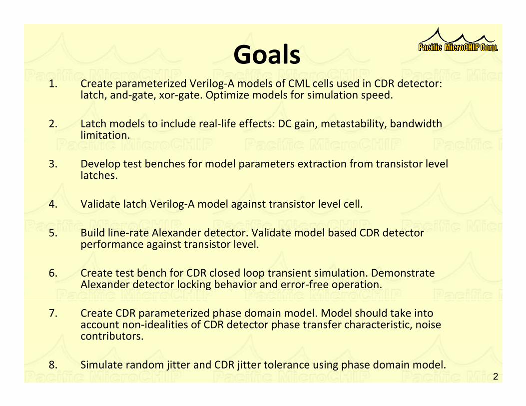
Goals1. Create parameterized Verilog-A models of CML cells used in CDR detector:
latch, and-gate, xor-gate. Optimize models for simulation speed.
2. Latch models to include real-life effects: DC gain, metastability, bandwidth limitation.
3. Develop test benches for model parameters extraction from transistor level latches.
4. Validate latch Verilog-A model against transistor level cell.
5. Build line-rate Alexander detector. Validate model based CDR detector performance against transistor level.
6. Create test bench for CDR closed loop transient simulation. Demonstrate Alexander detector locking behavior and error-free operation.
7. Create CDR parameterized phase domain model. Model should take into account non-idealities of CDR detector phase transfer characteristic, noise contributors.
8. Simulate random jitter and CDR jitter tolerance using phase domain model.

3
CML Latch ModelMetastability
During latching output voltage can be
expressed as:
V=V0*e(A-1)*t/RC, where A - DC gain, V0 -
initial output voltage.
Driving latch with close to zero signal and
switching from track to hold mode will
cause latch output voltage rise (or fall)
exponentially. In order to properly model
this effect regeneration time constant
RC/(A-1) should be found. It can be done
by simulating transistor level latch during
latching and registering times t1 and t2
such as latch output voltage V2/V1=e.
That way voltage at the latch output
can be expressed:
V=V0*et/(t2-t1)
Bandwidth limitation
Bandwidth limitation causing latch
output to slew. Bandwidth limitation
can be modeled using first order low-
pass filter. Verilog-A first order low-
pass filter can be expressed as Laplace
transformation:
V=laplace_nd(V0,{1},{1, Tau})
Where Tau is RC time constant, found
by measuring latch output signal
rise/fall time in transistor level
simulation at 10%-90%. Then Tau:
Tau=Trf/ln(9.0)
DC Gain
DC gain can be derived from transistor
level DC simulation.
Slope of Vout/Vin characteristic can be
used in conjunction with clipping
function (representing output voltage
limitation):
V=min(Vmax,max(Vmin,Av*Vin)
Other solution could be soft-clipping
using hyperbolic tangent approximation,
but will result in slower simulation.

4
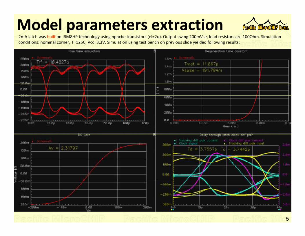
Model parameters extractionCreated CML latch model is characterized by following parameters:
Vswse - single ended output swing (V).
Av - latch DC gain in track mode (times)
Tmet - latch regeneration time constant. It’s derived from schematic latch simulation. Latch is switched from track to hold mode while
data input is unbalanced by 100uV. Time interval needed for latch output voltage to change 2.71828 times is Tmet.
Td - delay caused by data input signal propagation through tracking diff pair. It is measured as a time delay between zero crossings
of the input signal and the collector current of tracking diff pair transistors.
Tc - delay caused by clock input signal propagation through clock diff pair. It is measured as a distance between zero crossings of
input the clock signal and the collector current of clock diff pair transistors.
Trf - averaged rise/fall time measured at 10%-90% levels.
Parameters extraction is performed using transistor level simulation. The latch cell has 2 views: “schematic” and “veriloga”. During
parameters extraction Cadence Hierarchy Editor should point to latch instances schematic view. All measurements are automated and
shown on waveform window. Simulation schematic, waveform state and simulator state are provided (CDR_VA/SIM_LATCH).
5
2mA latch was built on IBM8HP technology using npncbe transistors (el=2u). Output swing 200mVse, load resistors are 100Ohm. Simulation
conditions: nominal corner, T=125C, Vcc=3.3V. Simulation using test bench on previous slide yielded following results:
Model parameters extraction

6
3.76pTd
192mVVswse
3.74pTc
10.48pTrf
11.07pTmet
2.32Av
Extracted ValueParameter
Model ValidationLatch cell instances switched to “veriloga” view in the Hierarchy editor. Extracted
parameters are fed back to Verilog-A model through latch symbol properties.

7
Model ValidationComparison of the Verilog A based latch with previously simulated real latch.

8
AND, XOR Gates Models(located in CDR_VA/AND_VA & XOR_VA)
Created CML AND and XOR gate models are characterized by the following parameters:
Vswse - single ended output swing (V)
Av - DC gain of gate’s signal diffpair (times)
Trf - averaged output rise/fall time measured at 10%-90% levels.
The DC gain and bandwidth limitations in these Verilog-A models are implemented in the same
way as in the latch model. Since, the phase detector performance depends mostly on latch
characteristics, we don’t extract actual XOR/AND parameters even though Vswse, Av an Trf can
be derived from transistor level schematics in the same way as it was done for the latch. We
assume that Av and Trf parameters for the gates are the same as for latches we analyzed:
Av=192mV, Trf=10.48ps, Av=2.32

9
Alexander detector schematic(located in CDR_VA/ALEX_DET)
10
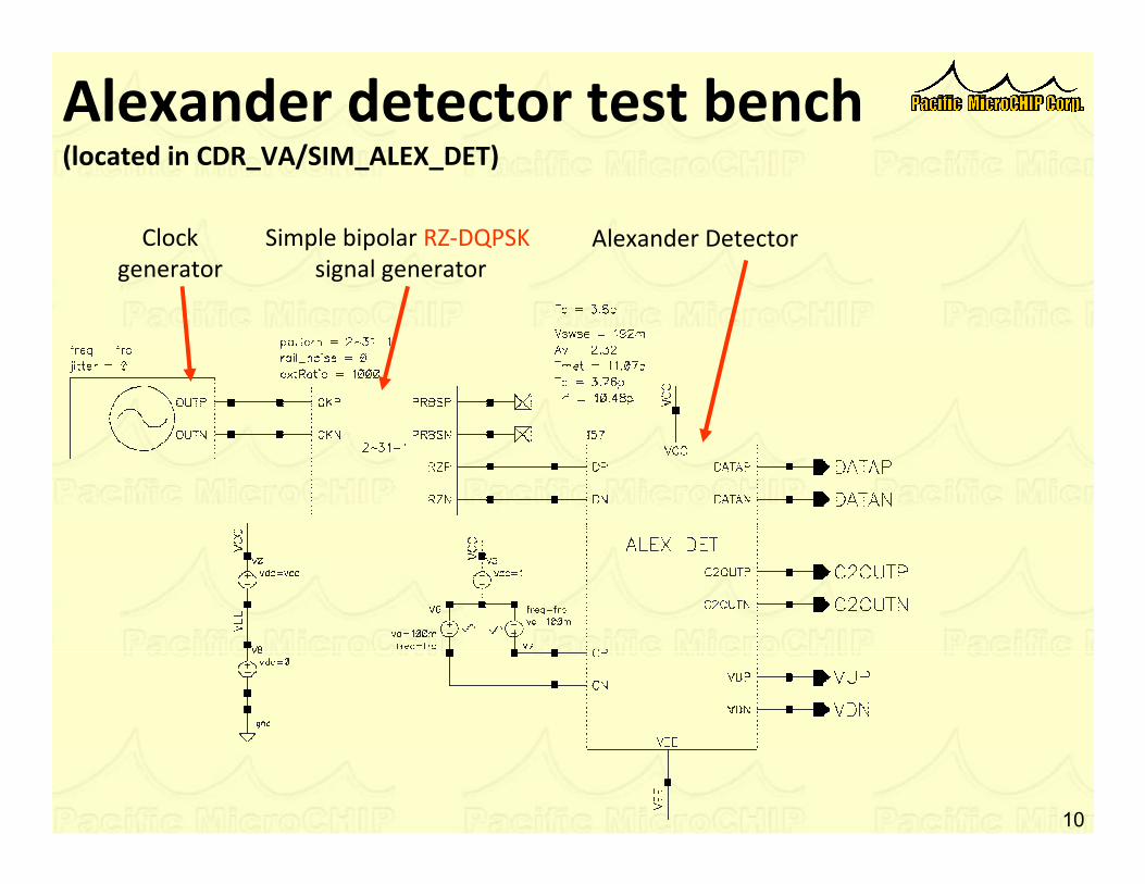
Alexander detector test bench(located in CDR_VA/SIM_ALEX_DET)
Clock
generator
Simple bipolar RZ-DQPSK
signal generator
Alexander Detector

11
Detector Phase Transfer- Model vs Schematic comparison
25Gbps RZ-DQPSK data is applied to the input. Three cases of data quality is considered:
1) clean input 2) 5ps p-p jitter + 20mV rail noise 3) 10ps p-p jitter + 20mV rail noise
12
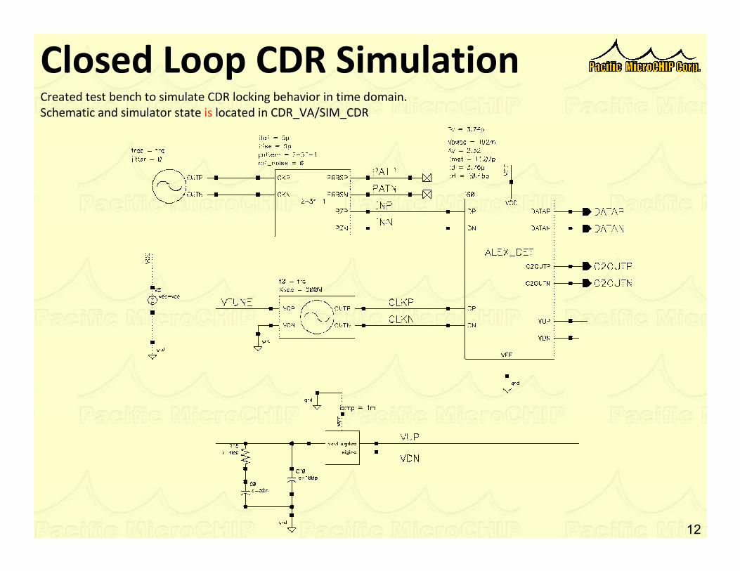
Closed Loop CDR SimulationCreated test bench to simulate CDR locking behavior in time domain.
Schematic and simulator state is located in CDR_VA/SIM_CDR
13
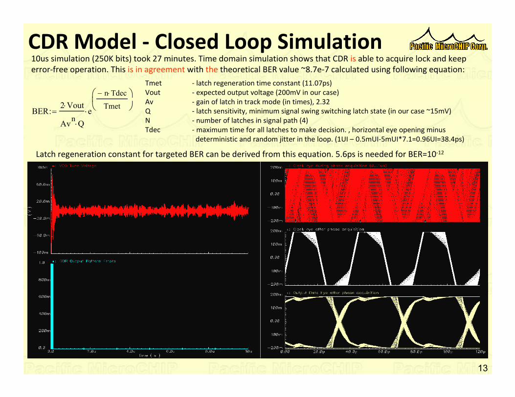
CDR Model - Closed Loop Simulation10us simulation (250K bits) took 27 minutes. Time domain simulation shows that CDR is able to acquire lock and keep
error-free operation. This is in agreement with the theoretical BER value ~8.7e-7 calculated using following equation:
BER2 Vout⋅
AvnQ⋅
e
n− Tdec⋅
Tmet
⋅:=
−
Tmet - latch regeneration time constant (11.07ps)
Vout - expected output voltage (200mV in our case)
Av - gain of latch in track mode (in times), 2.32
Q - latch sensitivity, minimum signal swing switching latch state (in our case ~15mV)
N - number of latches in signal path (4)
Tdec - maximum time for all latches to make decision. , horizontal eye opening minus
deterministic and random jitter in the loop. (1UI – 0.5mUI-5mUI*7.1=0.96UI=38.4ps)
Latch regeneration constant for targeted BER can be derived from this equation. 5.6ps is needed for BER=10-12

14
10us simulation (250K bits) took 15 hours. Simulation test bench/setup is same as before. The latch is represented by
schematic, and the rest is based on verilog-A. The time domain simulation shows CDR locking and error free operation.
CDR Schematic - Closed Loop Simulation
15
CDR Phase Domain Model.Theory.
The time domain CDR model even though allowing much shorter simulation times (compared to schematics) won’t be able to predict jitter
tolerance of CDR at low jitter frequencies. The phase domain model has no such limitations since it eliminates time domain information within
clock cycle and represents clock and data signal transitions by their phases. BER prediction is based on the fact that CDR produces error-free
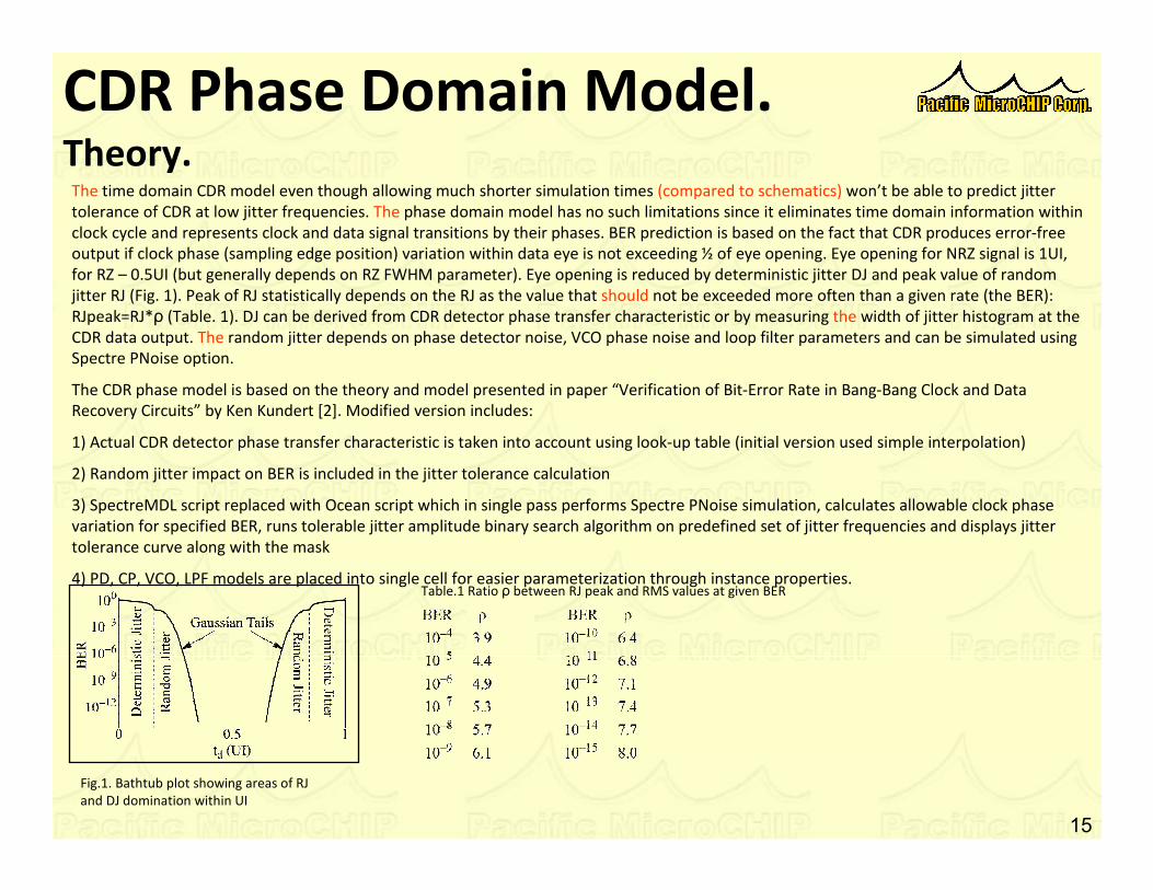
output if clock phase (sampling edge position) variation within data eye is not exceeding ½ of eye opening. Eye opening for NRZ signal is 1UI,
for RZ – 0.5UI (but generally depends on RZ FWHM parameter). Eye opening is reduced by deterministic jitter DJ and peak value of random
jitter RJ (Fig. 1). Peak of RJ statistically depends on the RJ as the value that should not be exceeded more often than a given rate (the BER):
RJpeak=RJ*ρ (Table. 1). DJ can be derived from CDR detector phase transfer characteristic or by measuring the width of jitter histogram at the
CDR data output. The random jitter depends on phase detector noise, VCO phase noise and loop filter parameters and can be simulated using
Spectre PNoise option.
The CDR phase model is based on the theory and model presented in paper “Verification of Bit-Error Rate in Bang-Bang Clock and Data
Recovery Circuits” by Ken Kundert [2]. Modified version includes:
1) Actual CDR detector phase transfer characteristic is taken into account using look-up table (initial version used simple interpolation)
2) Random jitter impact on BER is included in the jitter tolerance calculation
3) SpectreMDL script replaced with Ocean script which in single pass performs Spectre PNoise simulation, calculates allowable clock phase
variation for specified BER, runs tolerable jitter amplitude binary search algorithm on predefined set of jitter frequencies and displays jitter
tolerance curve along with the mask
4) PD, CP, VCO, LPF models are placed into single cell for easier parameterization through instance properties.
Fig.1. Bathtub plot showing areas of RJ
and DJ domination within UI
Table.1 Ratio ρ between RJ peak and RMS values at given BER
16
Phase domain model is based on Verilog-A. Symbol and Verilog views are located in CDR_VA/PHASEMOD cell. Simulation schematic - SIM_JTOL.
Steps:
1) Set loop filter parameters in SIM_JTOL schematic.
2) Enter CDR parameter into Ocean script file “JTOL.ocn” (see below). Ocean script “JTOL.ocn” is included in delivered archive.
/********************************/
/* Specification of CDR parameters */
/********************************/
;Jitter tolerance mask specified in frequency:amplitude, where frequency in [Hz], jitter amplitude in [UI].
jmask=list(25.0:15.0 6.0K:15.0 60.0K:1.5 1.0M:1.5 10.0M:0.15 2.5G:0.15 24.0G:0.15);
fpoints=5 ; amount of frequency points used to simulate jitter tolerance between specified mask corners.
tol=0.001 ; accuracy of jitter tolerance measurement.
eyeOpening=0.5 ; eye opening in UI without RJ and DJ taken into account. For NRZ eyeOpening=1UI, for RZ-0.5UI.
Fvco=25.0G ; f0 of VCO [Hz].
Kvco=0.6G ; Kvco [Hz/V].
Svco=-100.0 ; VCO phase noise [dBc].
DFvco=1.0M ; frequency offset at which VCO phase noise is specified.
XFERpd="xfer_sch.dat" ; path to detector phase transfer lookup-table file. Generated from Spectre simulation using ocnPrint command.
mVpd=1.0 ; detector phase transfer characteristic voltage scaling factor applied to values from lookup table.
Spd=100n/50G ; detector and charge pump noise spectral density (A^2/Hz). For simplicity it can be assumed to be flat over frequency, so
; pd_S=N/(f2-f1). The noise (N) can be found by driving the detector with half-data rate periodic input signals shifted 90°.
; Then SpectreRF PNoise analysis is used to get the output noise.GMcp=1m ; charge pump Gm.
3) Run script by issuing command loadi(“JTOL.ocn”) from Cadence CIW window
4) Script performs Spectre PNoise and AC simulation, calculates allowable clock phase variation for specified BER, runs tolerable jitter amplitude
binary search algorithm on predefined set of jitter frequencies and displays jitter tolerance curve along with mask. At the end of script run? RJ
rms value [in UIs] is reported in icfb window and simulation results are plotted in a new waveform window. Following are waveform names
available for further manipulation/plotting through Cadence calculator:
jtol_w (jitter tolerance waveform),
mask_w (mask waveform),
jxfer_w (phase transfer waveform).
CDR Phase Domain Model.Instructions.

17
CDR Phase Domain Model. Results.The simulation of 25 frequency points of the jitter tolerance curve took 10 minutes. The resulting CDR jitter transfer and jitter tolerance
curves are shown below. Simulation using CDR detector phase transfer lookup table from schematic and Verilog model yielded identical
JTOL curve. Jitter transfer characteristic is impacted by non-linearities in detector phase transfer characteristic.
18
Conclusions� CML latch Verilog-A parametric model is designed. The methodology and necessary tools (simulation
schematic, simulator states etc.) are developed for parameter extraction from transistor level CML latch. Main
CML latch effects impacting CDR detector performance are taken into account: metastability, gain, bandwidth
limitations and physical signal delays through the latch structure. The model accurately represents transistor
level latch at the same time reducing the simulation times up to ~30 times. Using similar approach CML AND
and XOR gates verilog-A models are build.
� Full-rate Alexander phase detector schematic is built. The schematic can be simulated using latches
represented by the transistor level or parametrical Verilog-A model. The detector phase transfer characteristics
were simulated and compared using both model and schematic at different input data jitter values.
� Verilog-A Models of bipolar RZ PRBS source and VCO are designed to make possible CDR closed loop
simulation. A test bench utilizing these models along with CDR detector schematic is created. The test bench
allows to induce jitter into CDR input data stream and to vary VCO and loop filter parameters. The simulation of
250K RZ DQPSK bits transmission at 25Gpbs took about 30 minutes and show CDR ability to acquire lock and
keep error-free operation. The same simulation but with latches represented by transistor level took 15 hours,
showing same CDR performance. Simulation results are presented.
� The phase domain model, test bench and supporting Ocean script is created to overcome the time domain
approach limitations in CDR jitter tolerance and jitter transfer simulations. The phase domain approach takes
into account random and deterministic jitter, actual detector phase transfer characteristic (derived from Verilog-
A or schematic simulation), charge-pump Gm and noise, VCO gain and phase noise, loop filter parameters.
Jitter tolerance curve simulation, covering SONET/SDH 7-corner mask (scaled in frequency axis 2.5 times),
takes about 5 minutes.
� All above described verilog models, libraries and scripts are included in deliverables package.
19
Materials Used
[1] Cadence®Verilog®-A Language Reference 6.1
[2] Ken Kundert . Verification of Bit-Error Rate in Bang-Bang Clock and Data Recovery Circuits
[3] William Evans. Comparator Metastability Analysis
[4] Jri Lee, Ken Kundert, Behzad Razavi. Modeling of Jitter in Bang-Bang Clock and Data Recovery Circuits
Acrobat Document
Archive with DeliverablesContents:
CDR_VA - Cadence library with all schematics, simulator states and waveform setups
JTOL.ocn - jitter tolerance simulation Ocean script
xfer_sch.dat - phase detector phase transfer characteristic lookup table data generated from schematic
xfer_va.dat - phase detector phase transfer characteristic lookup table data generated from VerilogA model
CDR_Model.zip