vapor–liquid–solid growth of semiconductor nanowires
TRANSCRIPT

Chapter 1Vapor–Liquid–Solid Growth of SemiconductorNanowires
Heon-Jin Choi
Abstract Nanowires make possible to manipulate light in novel methods and thusare promising materials for advanced optoelectronics. To exploit the potential,the growth behavior has to be controlled since it dominates the physical andchemical states and, in turn, the optical properties of nanowires. In this chapter, thevapor–liquid–solid (VLS) mechanism for the growth and modulation of nanowireswas discussed. The chapter first reviewed the fundamental aspects of the VLSmechanism. Then the state of the art of the growth and modulation of nanowiresfor optoelectronics were discussed from the point of view of the critical issuespertaining to this mechanism. Some examples of optoelectronic devices that hadbeen fabricated based on the VLS mechanism were also reviewed in an effortto cover the cutting edge technology in this area. Lastly, a summary and severaldifferent perspectives on the VLS mechanism were presented.
1.1 Introduction
Nanowires are hair-like, one-dimensional (1D) nanomaterials with diameters in thesub-one hundred nanometer scale and lengths ranging from several hundreds of nmto as high as a few cm. Owing to their nanoscale dimensions in the radial direction,they have size confinement effects that give them novel physical properties ascompared to bulk materials. Their one-dimensional geometry on the nanometerscale provides an extremely high surface area with a nanoscale radius of curvatureand great mechanical flexibility with near theoretical strength. These properties areadvantageous in many chemical and mechanical applications. The geometry also
H.-J. Choi (�)Department of Materials Science and Engineering, Yonsei University, 50 Yonsei-ro,Seodaemun-gu, Seoul 120-749, Koreae-mail: [email protected]
G.-C. Yi (ed.), Semiconductor Nanostructures for Optoelectronic Devices,NanoScience and Technology, DOI 10.1007/978-3-642-22480-5 1,© Springer-Verlag Berlin Heidelberg 2012
1

2 H.-J. Choi
provides anisotropic properties that should be interesting from the point of view ofnanomaterials science and engineering. Their length, reaching as high as the cmscale, makes them easy to manipulate for device fabrication.
Nanowires are promising materials for advanced optoelectronics. In addition tothe unique aspects of their physical, chemical, and mechanical properties, the sizeof these materials is comparable to visible light in wavelength from 400 to 650 nm.This implies that nanowires can be used to handle light on a nanometer scale andthus can be used as building blocks for advanced optoelectronics. Indeed, novelmethods of the manipulation of light with nanowires, including nanoscale Fabry–Perrot mode stimulated emission, wave guiding of photons, random lasing action,highly efficient luminescence, and extremely sensitive photodetection, have recentlybeen demonstrated. The concept of many advanced nanowire-based optoelectronicdevices including light-emitting diodes (LEDs), lasers, optical sensors, photodiodes, and photovoltaic cells have also been demonstrated.
The physical and chemical states of nanowires dominate their optical properties.The length and diameter of nanowires as well as their alignment affect the emissionand absorption properties. The composition, impurity, or doping level, defectconcentration, crystal structure, growth direction, and nature of the facets are alsocritical to the emission and/or stimulated emission and absorption. It should benoted that these physical and chemical states are closely related to the growth ofnanowires. Therefore, one must fully understand the growth behavior of nanowiresand develop rational, reliable growth processes to exploit the potential of nanowiresin optoelectronics.
Nanowires are a result of anisotropic, 1D crystal growth on a nanometer scale.Therefore, the key issue related to the growth of nanowires is how to induce1D crystal growth in a controlled manner. Regarding this, many approaches havebeen studied, including the use of the metal-catalyst-assisted vapor–liquid–solid(VLS) mechanism, the vapor–solid (VS) mechanism, and the template-assisted (TA)mechanism. Among these, the VLS mechanism is the most widely used owing to itssimplicity and versatility when applied in many semiconductor systems.
This chapter reviews the growth of semiconductor nanowires by the VLSmechanism in the area of optoelectronics. As mentioned earlier, the growth processis critical to the physical and chemical state of nanowires and thus their opticalproperties. Therefore, a review of the growth process may be helpful so as tofacilitate the preparation of superior nanowires for optoelectronics. This chapterfocuses on the VLS mechanism. This may, however, limit our viewpoint regardingthe growth of nanowires, as other mechanisms are also available. However, the VLSmechanism is a mainstay at present. Therefore, it may be sufficient to review thestate of the art of this area. This chapter seeks to explain the understanding of whatthe VLS mechanism is as well as the manner in which better nanowires can be grownfor optoelectronics. Accordingly, the chapter first reviews the fundamental aspectsof the VLS mechanism. The growth of nanowires and a number of critical issuespertaining to VLS mechanism follow. Some examples of optoelectronic devices thathave been fabricated based on the VLS mechanism are also reviewed in an effort

1 Vapor–Liquid–Solid Growth of Semiconductor Nanowires 3
to cover the cutting edge technology in this area. Lastly, a summary and severaldifferent perspectives on the VLS mechanism are presented.
1.2 VLS Mechanism for One-Dimensional Crystal Growth
The VLS mechanism is a 1D crystal growth mechanism that is assisted by a metalcatalyst. It results in the creation of whiskers, rods, and wires. 1D crystal growthwas initially developed nearly 50 years ago in the Si industry and the mechanismwas suggested for wider use by Wagner in 1964 [1]. Figure 1.1 shows a schematicof the VLS mechanism. In this mechanism, the metal catalyst forms liquid alloydroplets at a high temperature by adsorbing vapor components. For some reason,e.g., temperature or vapor pressure fluctuation, the alloy is further supersaturated;i.e., it becomes a solution in which the actual concentration of the components ishigher than the equilibrium concentration. It then drives the precipitation of thecomponent at the liquid–solid interface to achieve minimum free energy of thealloy system. Accordingly, the 1D crystal growth begins, and it continues as longas the vapor components are supplied. Because vapor (carries solid components),liquid (catalyst alloy), and solid (precipitated one-dimensional structures) phasesare involved, it is known as the VLS mechanism. At a glance, one can know thatthe size and position of the catalyst are related to the diameter and position of the1D structures, as the liquid phase is confined to the area of the precipitated solidphase.
Fig. 1.1 Growth of 1D structures by VLS mechanism

4 H.-J. Choi
The mechanism works at a high temperature at which the metal catalyst forms aliquid alloy. Therefore, chemical processes that occur at high temperatures, such aschemical vapor deposition (CVD), molecular beam epitaxy (MBE), laser ablation(LA) and carbothermal reduction (CR), are generally used in conjunction with themechanism. Occasionally, metal catalysts sometimes work in a solid state in a vaporor liquid phase environment in a process termed the VSS (vapor–solid–solid) or LSS(liquid–solid–solid) mechanism.
Since the 1970s, the mechanism has been used to grow various types ofwhiskers on the micrometer or mm scale. A typical example is SiC whiskers, whichare excellent reinforcements for high-strength, high-toughness ceramic or metalcomposites [2]. In this application, larger whiskers have a better reinforcing effect;thus, the catalyst size is made to be as large as possible, up to more than 10 �m, togrow large-diameter SiC whiskers, as shown in Fig. 1.2.
The mechanism was then noted for the growth of 1D structures on a nanometerscale, i.e., nanowires, in the 1990s, and the feasibility of this was demonstratedby several groups, including the Lieber group at Harvard University, the Yanggroup at the University of California Berkeley, and the Samuelson group at LundUniversity. As this mechanism was slated to become a core method for the growth ofsemiconductor nanowires, unambiguous experimental evidence of this mechanismwas required for further study. Regarding this, Yu directly observed the growth ofGe nanowires by using an in situ high-temperature transmission electron microscope[3]. The findings of Yu’s study showed that there are three well-defined stages in theVLS mechanism: alloying (note that the catalyst in Fig. 1.3a–c becomes larger asthe Ge component dissolves and becomes alloyed with Au), precipitation of Ge(the bright area in c and d), and axial growth (extended structures in e and f).
Fig. 1.2 SiC whiskers grown by VLS mechanism using Fe as catalyst (after [2])

1 Vapor–Liquid–Solid Growth of Semiconductor Nanowires 5
Fig. 1.3 Direct observationof growth of 1D Ge structuresby VLS mechanism using Auas catalyst (after [3])
This observation clearly supports the proposed VLS mechanism, which is shown inFig. 1.1. Other observations regarding the growth of Si nanowires on the substratefurther confirmed the working of the VLS mechanism with the assistance of a liquidcatalyst [4].
The brief history of the VLS mechanism implies that it can be generally usedfor the growth of many 1D structures, from the nm to even the mm scale. It alsoshows the rising of new technology from old technology as a good example of theprogress of science and technology from previous studies. In fact, previous studieshave established some fundamental aspects, as discussed below, which are essentialfor growing 1D structures using a catalyst.
1.2.1 Requirements for Metal Catalyst
Metal catalysts are essential in the VLS mechanism, but not all metals can work.These meet the following requirements: (1) It must form a liquid solution with acomponent of the solid phase. (2) The solubility limit of the catalyst componentin the liquid phase must be much higher than that in the solid phase (i.e.,K D Cs=Cl < 1, where Cs is the solubility limit in the solid phase and Cl is thesolubility limit in the liquid phase). Under this condition, the catalyst easily leadsto the formulation of the liquid alloy with little contamination in the solid phase.(3) The vapor pressure (Vp) of the catalyst component over the liquid alloy shouldbe small. Otherwise, the catalyst will evaporate and eventually disappear in thecourse of growth. (4) It must be inert to chemical reactions. Otherwise, a reactioncould deprive it of its catalytic function. (5) It must not make an intermediate solid.Otherwise, the intermediate solid will also deprive it of its catalytic function [1].
Previous studies have revealed that some metals meet the requirements. Gener-ally, noble and transition metals work well with the VLS mechanism. For example,

6 H.-J. Choi
Au works well for the growth of a 1D structure of group IV materials (e.g., Si andGe), oxides (e.g., ZnO), and III–V semiconductors. Transition metal such as Ni andFe also work for the growth of group IV materials (e.g., Si, Ge, and SiC) and III–Vsemiconductors. Naturally, many studies have focused on these metals to grow 1Dstructures. However, it should be noted that many other metals can also be developedas a catalyst for the VLS mechanism [5].
1.2.2 Phase Diagram
Because the adsorption, dissolving, mixing, diffusion, and precipitation in the liquidphase are thermodynamic processes that work toward equilibrium, a phase diagramis useful to predict how a catalyst will work. Figure 1.4 shows the phase diagram ofthe Au–Si system, which can be referred to regarding the growth of 1D Si structureswith Au [6]. The diagram indicates that the minimum growth temperature for Sishould be higher than the eutectic point of the system (364ıC). The diagram alsoindicates that the composition of the Au–Si alloy above the eutectic point will followthe liquidus line (solid line) that denotes equilibrium between the solid and liquidphase. Therefore, the composition of the liquid alloy can be found at the liquidusline (point A) at a given temperature (1;100ıC in the diagram). However, sometemperature or vapor pressure fluctuation over the liquid alloy dissolves more Si
Fig. 1.4 Phase diagram of Au–Si system with indication of the composition of liquid alloy catalystin the course of growth of 1D structures by VLS mechanism

1 Vapor–Liquid–Solid Growth of Semiconductor Nanowires 7
than the equilibrium composition and renders it into a supersaturated state. Asa result, the composition of the alloy goes beyond the equilibrium composition,moving to the right side of the liquidus line (solid arrow). This supersaturationstate is thermodynamically a nonequilibrium and unstable state and thus drivesthe precipitation of the solid phase from the supersaturated liquid alloy until anequilibrium state is reached. The composition will then move back to the left andreach the liquidus line (dashed arrow). The composition of the precipitated solidphase corresponds to that of the phase boundary and thus is pure Si according to thediagram (dashed dot arrow). Meanwhile, the composition of the alloy goes beyondthe equilibrium composition again as Si is dissolved from the vapor and drives theadditional growth of 1D structures with the precipitation at the interfaces.
It should be noted that the currently available phase diagrams are constructedfrom bulk systems. Because the thermodynamic properties of a nanosystem arewholly different from those of a bulk system, the phase diagram of the type ofnanometal catalyst that we are interested in should differ from that of the bulksystem. Indeed, Eli and Peter Sutter investigated the equilibrium composition ofnanoscale Au–Ge alloy droplets at the tips of Ge nanowires and found that theequilibrium composition of these droplets deviates significantly from that of the bulkalloy (Fig. 1.5) [7]. Adhikari et al. also investigated Au-catalyzed Ge nanowireand constructed a binary Au–Ge phase diagram that shows the catalyst size-dependent liquidus temperature [8]. These phenomena may be due to the criticalrole of the surface energy in the nanosystem [7–10]. Regardless of the cause ofthe deviation, it should be considered that the different thermodynamic equilibriumof the nanosystem causes discrepancies between the actual growth behavior ofnanowires through a nanometal catalyst and predictions on the basis of a diagram ofthe bulk system.
Fig. 1.5 Au–Ge binary alloy phase diagram. The solid gray curves represent the Au and Geliquidus and solidus lines, respectively. Squares represent measurements of the temperature-dependent Ge content of Au–Ge alloy drops at the tip of Ge nanowires (after [7])

8 H.-J. Choi
1.2.3 Kinetics and Rate-Determining Step
Three phases (gas, liquid, and solid) and two interfaces (gas/solid and liquid/solid)are involved in the VLS mechanism. In these complex system, the kinetics of theVLS mechanism consists of four steps: (1) mass transport in the gas phase; (2)chemical reaction at the vapor–liquid interface; (3) diffusion in the liquid phase; and(4) incorporation of atoms in a crystal lattice (Fig. 1.6) [11–14]. Identification of therate-determining step among these is important to control the overall kinetics ofthe VLS mechanism. However, this is complicated, as three phases, two interfaces,and chemical reactions are involved [11]. Nevertheless, it may be possible to drawsome insight based on the experimental results. As an example, the rate-determiningstep for the growth of 1D Si structures with an Au catalyst could be postulatedas follows: Among the steps, step (3) can be excluded, because atoms diffuse inliquid metals very quickly [12] and thick nanowires or whiskers do not grow moreslowly than those that are thinner, while the shape of the liquid droplet is maintainedas nearly hemispherical and thus retains a longer diffusion length [11]. Step (1)can also be excluded because the diffusion coefficient in the gaseous phase usuallyfollows the following power law: D D Do.T=To/n.P=Po/, n D 1:5 � 2 [11, 12].Therefore, the growth rate should follow the power law. However, this is not thecase in many cases [11–14]. The primary evidence for regarding step (2) as therate-limiting step is that the growth rate is proportional to the partial pressure ofthe reactant gas. However, this does not fully support the argument given that thegrowth process consists of two activated steps in series [11]. The dependence ofthe growth rate on the reactant vapor concentration is not in itself evidence that anyof the steps is the rate-determining step. Rather, it simply reflects the dependenceof the growth rate on supersaturation. Therefore, the rate-determining step wouldbe step (4), the incorporation of atoms in a crystal lattice. It should be noted thatthe rate-determining step can be changed by the materials involved in the kineticsand by the processing conditions. Therefore, it should be carefully postulated by
Fig. 1.6 Kinetic steps inVLS mechanism: (1) masstransport in the gas phase; (2)chemical reaction on thevapor–liquid interface; (3)diffusion in the liquid phase;and (4) in corporation ofatoms in a crystal lattice

1 Vapor–Liquid–Solid Growth of Semiconductor Nanowires 9
as many experimental results and data as possible. In fact, the postulation here ispossible because a considerable amount of experimental data regarding the growthof Si whiskers, rods, and recently nanowires is available in the literature.
1.2.4 Size of the Metal Catalyst
As described earlier, nanowires can be grown using a nanometer-sized metal catalystbecause the diameter of a 1D structure is confined by the size of the catalyst. Indeed,the bulk of previous studies demonstrated the growth of nanowires using nanofilms(that convert to nanoliquid droplets at a high temperature due to surface tension)or nanoparticles. However, it is difficult to decrease the size of the catalyst and inturn the diameter of nanowires in an unlimited manner. Thermodynamically, theminimum radius of a liquid metal droplet is given as [15]
Rm D 2Vl
RT ln.s/�lv; (1.1)
where Vl is the molar volume of the droplet, �lv is the liquid–vapor surface energy,and s is the degree of supersaturation of the vapor. According to this equation, usinga smaller catalyst requires a higher degree of supersaturation. However, the chemicalpotential of the component in the metal–alloy catalyst becomes high as the size ofthe catalyst decreases due to the Gibbs–Thompson effect:
�� D 2�
r: (1.2)
Here, �� is the chemical potential difference of the component species in the liquiddroplet, � is the surface energy, and r is the radius of curvature of the droplet.Therefore, dissolving a vapor component into a liquid alloy becomes increasinglydifficult as the size decreases, making it difficult to reach supersaturation states thatsufficiently induce the growth of nanowires. Indeed, it is known that the growth of1D structures with diameters of several tenths of nm is feasible; however, ensuring asmaller diameter (e.g., sub-10 nm) is difficult due to the thermodynamic limitationsassociated with the use of a nanocatalyst.
An additional difficulty that arises when downsizing a catalyst comes from themanipulation of metal nanoparticles or droplets. It is well known that nanoparticleshave strong van der Waals attractive forces and thus agglomerate into larger parti-cles. Furthermore, Ostwald ripening occurs between nanoparticles at high tempera-ture. Ostwald ripening is a spontaneous process that occurs because larger particlesare more energetically favorable. Accordingly, nanoparticles tend to transform intolarge particles to attain a lower energy state if the temperature is high enough toinduce diffusion of the metal component. Because the van der Waals attractiveforces and Ostwald ripening lead to the formation of larger droplets, larger diameter1D structures are often grown from a nanometal catalyst. Thus, metal nanoparticles

10 H.-J. Choi
have to be carefully separated from each other in the course of the preparation,positioning on the substrate, and heating for the growth of 1D structures.
1.3 Growth of Nanowires by the VLS Mechanism and CurrentIssues for Optoelectronics
1.3.1 Growth of Semiconductor Nanowires by the VLSMechanism
Si nanowires are a typical case of the growth of nanowires by the VLS mechanismwith the assistance of a metal catalyst. Typically, Si nanowires are grown by Aubecause this metal meets the requirements for a VLS catalyst. The eutectic pointof the Au–Si system is low, the phase relationship is simple and the system isstable at high temperatures. Figure 1.7 shows Si nanowires grown by the VLSmechanism using Au as a catalyst and SiCl4 as the Si precursor [16]. The SEMimages shown in Fig. 1.7a reveal Si nanowires with diameters of � 100 nm andlengths of several �m that were grown on a Si substrate coated with Au film with athickness of 2 nm. It also shows that the nanowires grew vertically on the substrate.It is well known that an epitaxial relationship between the substrate and nanowirescan be attributed to the vertical growth of nanowires [17]; thus, the vertical growthhere indicates that Au yields epitaxial interfaces between the nanowires and Sisubstrate. The transmission electron microscopy (TEM) images and selected areaelectron diffraction (SAED) patterns in Fig. 1.7b clearly show that the Si nanowiresare single-crystalline nanowires without any structural defects. Alloy globules ofAu–Si formed at the tips of the nanowires. An energy-dispersive spectroscopy(EDS) analysis across the catalyst–nanowire interface at the tip of an individualnanowire shows that Au operates as a VLS catalyst in this case. Note that an Au-richglobule formed when the Au catalyst was used according to the phase diagram of theAu–Si binary system (Fig. 1.4). Characterization of the catalyst globule/nanowireinterfaces by high-resolution transmission electron microscopy (HRTEM) reveals
0 50 100Distance (nm)
150 2000
1000
2000
2 nm 2 nm30mm
Cou
nt 3000
4000C dba 5000
SiAuO
Fig. 1.7 Si nanowires grown by VLS mechanism using Au as catalyst. The nanowires were grownin the [110] direction for (110) Si substrates. (a) SEM image of Si nanowires, (b) TEM image anddiffraction pattern, (c) EDS analysis of catalyst, (d) HRTEM image of the interface (after [16])
1 Vapor–Liquid–Solid Growth of Semiconductor Nanowires 11
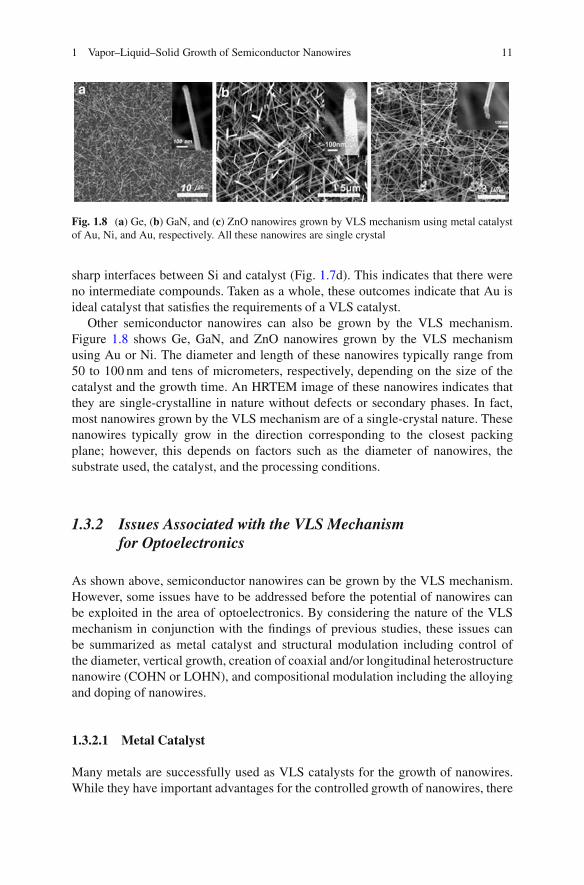
Fig. 1.8 (a) Ge, (b) GaN, and (c) ZnO nanowires grown by VLS mechanism using metal catalystof Au, Ni, and Au, respectively. All these nanowires are single crystal
sharp interfaces between Si and catalyst (Fig. 1.7d). This indicates that there wereno intermediate compounds. Taken as a whole, these outcomes indicate that Au isideal catalyst that satisfies the requirements of a VLS catalyst.
Other semiconductor nanowires can also be grown by the VLS mechanism.Figure 1.8 shows Ge, GaN, and ZnO nanowires grown by the VLS mechanismusing Au or Ni. The diameter and length of these nanowires typically range from50 to 100 nm and tens of micrometers, respectively, depending on the size of thecatalyst and the growth time. An HRTEM image of these nanowires indicates thatthey are single-crystalline in nature without defects or secondary phases. In fact,most nanowires grown by the VLS mechanism are of a single-crystal nature. Thesenanowires typically grow in the direction corresponding to the closest packingplane; however, this depends on factors such as the diameter of nanowires, thesubstrate used, the catalyst, and the processing conditions.
1.3.2 Issues Associated with the VLS Mechanismfor Optoelectronics
As shown above, semiconductor nanowires can be grown by the VLS mechanism.However, some issues have to be addressed before the potential of nanowires canbe exploited in the area of optoelectronics. By considering the nature of the VLSmechanism in conjunction with the findings of previous studies, these issues canbe summarized as metal catalyst and structural modulation including control ofthe diameter, vertical growth, creation of coaxial and/or longitudinal heterostructurenanowire (COHN or LOHN), and compositional modulation including the alloyingand doping of nanowires.
1.3.2.1 Metal Catalyst
Many metals are successfully used as VLS catalysts for the growth of nanowires.While they have important advantages for the controlled growth of nanowires, there

12 H.-J. Choi
are some issues from the point of view of semiconductor engineering. For example,Au as a catalyst is used for the growth of many nanowires, including Si, Ge, ZnO,GaN, and GaAs. However, it inevitably becomes contaminated into the nanowiresas a result of contact between the liquid Au alloy and the semiconductor at a hightemperature [18]. This contamination can increase the impurity level in the bandgap and thus degrade the optical properties of nanowires. Furthermore, Au is notcompatible with current CMOS processes and thus is limited in terms of how itcan be introduced into the CMOS process. The very high diffusivity of Au inducesmigration of this metal on the surface of Si nanowires, making it difficult to controlthe growth precisely [19]. Accordingly, efforts to find a suitable catalyst that willnot degrade the optical properties of nanowires and that can be used in the CMOSprocess have been made.
For Si nanowires, Al is considered as a promising candidate because the Al–Sibinary phase diagram is similar to that of Au–Si. Indeed, limited studies have shownthe successful growth of Si nanowires using Al [20, 21]. For example, Ke et al.grew Si nanowires by thermal CVD using Al as the catalyst [20]. The Al, however,oxidized quickly, showing that a well-designed, airtight growth process is necessary.In their work, Ke et al. used high H2 and SiH4 partial pressures to suppress the Aloxidation.
The other candidate for Si nanowires is Pt. Pt is a noble metal and thus has similarphysical properties to Au. Indeed, Pt also successfully works as a catalyst for thegrowth of Si nanowires [16]. Figure 1.9 shows scanning electron microscopy (SEM)images and TEM images of Si nanowires grown using Pt as a catalyst. The size ofthe Si nanowires is comparable to that of nanowires grown by Au. In this case, they
1008060Distance (nm)
402000
400
800
1200
1600
Cou
nt
2000 SiPtO
2400a
d e f
b c
30 mm
40 µm
5 nm
2 nm
100 nm
MnSi
zone axis [011]
<111>
Fig. 1.9 Si nanowires grown by VLS mechanism with Pt (a, b, c) (after [16]) and Mn catalyst(d, e, f). (a), (d) SEM images of Si nanowires, (b), (e) TEM images of Si nanowires, (c), (f) EDSanalysts of catalyst

1 Vapor–Liquid–Solid Growth of Semiconductor Nanowires 13
grew vertically on the substrate. Hence, Pt yields an epitaxial interface betweenthe nanowires and the Si substrate. It appears that the growth rate is generally fasterthan it is with Au under the same conditions. The Si nanowires are single-crystallinestructures without any structural defects. Alloy globules of Pt–Si form at the tips ofthe nanowires. An EDS analysis across the catalyst–nanowire interface at the tip ofan individual nanowire clearly shows that the Pt operated as a VLS catalyst, similarto Au.
Transition metals can also be considered as the VLS catalyst for the Si nanowires.For example, Mn can be used to grow Si nanowires. As shown in Fig. 1.9, the Sinanowires grown with Mn as a catalyst are tens of �m in length and tens of nm indiameter. Compared to other metal catalysts, such as Au or Pt [16], Mn catalystslead to rather slow growth under the same growth conditions. The nanowires alsohave metal globules at their tips and, as shown in Fig. 1.9, consist of a Si–Mnalloy containing about 64% Si and 36% Mn. These globules clearly indicate thatthe nanowires were grown by the VLS mechanism with the assistance of Mn. Inaddition, there is no Mn in the nanowire body. These results indicate that manyother metals can also be explored to grow Si nanowires. In fact, Ag, Bi, Cd, Co, Cu,Dy, Fe, Ga, Gd, Mg, Ni, Os, Pb, Pd, Te, Ti, and Zn can be explored as VLS catalystsfor Si nanowires, as summarized by Shimit et al. [5].
GaN and ZnO nanowires are typically grown using a transition metal suchas Ni and Au, respectively. As mentioned earlier, these metal catalysts can alsoincrease the impurity level in the band gap and thus degrade the optical propertiesof nanowires. However, the M (metal catalyst)–Ga–N or the M–Zn–O system iscomplex compared to M–Si system. Therefore, it is likely that the number ofcatalysts available for these nanowires is limited as compared to Si nanowires. Whilemany catalysts should have been explored for GaN nanowires, successful growth hasnot been reported thus far. In the case of ZnO nanowires, Sn has been reported as aVLS catalyst [22].
With regard to the formation of the impurity level in the band gap [23],the self-catalytic VLS mechanism is interesting. This mechanism works with aliquid catalyst that is formed in an in situ mode. For example, it was found thatInAs nanowires can be grown without a metal catalyst [24]. Closer investigationrevealed that a liquid In catalyst which forms from the substrate leads the growthof nanowires. Vertically aligned InP nanowires were also grown without a metalcatalyst. It was revealed that temperature and precusor ratio control induces indiumdroplets to form on the surface and act as nucleation sites for nanowire growth [25].This self-catalytic VLS mechanism is not commonly used, but it has the potentialto grow nanowires without contamination of the catalytic components in somesemiconductor systems.
1.3.2.2 Structural Modulation
To realize novel optical properties and newly fabricated devices, structural modula-tion of nanowires, such as control of the diameter, alignment, and growth-position,

14 H.-J. Choi
Fig. 1.10 Band-gap modulation of Si structures as a function of size (after [26])
is needed. Creating heterostructures in the radial or longitudinal direction is alsocrucial.
Diameter control: The optical properties of nanowires are dependent on theirdiameter. For example, the band gap, which determines the wavelength of lumi-nescence, of semiconductor nanowires is renormalized by the diameter. Theoreticalpredictions of this type of band gap modulation are shown in Fig. 1.10, where theband gap of Si nanowires becomes wider as the diameter approaches the sub-10 nmscale [26]. Such small diameters also change the semiconductor characteristic ofSi from an indirect to a direct band gap [27]. These findings imply that the opticalproperties of nanowires with both indirect and direct band gaps can be tuned bydecreasing their diameter down to their Bohr exciton radius.
However, as described in Sect. 1.2, downsizing of the catalyst raises the chemicalpotential of the liquid alloy droplet and thus makes it difficult to grow nanowireswith such a small diameter. This is thus a challenging issue from the point of viewof thermodynamics. It should also be noted that these types of very thin nanowireshave been grown using the VLS mechanism, though the optical properties in thesecases have not been reported [28]. Therefore, these types of very thin nanowires canbe grown for the development of indirect-band-gap nanowire-based optoelectronics.
With diameter control of direct-band-gap semiconductors such as GaN or ZnO,nanowires can also be created with novel optical properties such as multicolorluminescence by the quantum confinement effect. Indeed, such a novelty has alreadybeen demonstrated in GaN, InP and ZnO nanowires in which shifts in the emissionspectra occur due to radial quantum confinement [29–31]. However, the growth ofthese nanowires reliably on the sub-10 nm scale using the VLS mechanism remainsa challenging issue.
1 Vapor–Liquid–Solid Growth of Semiconductor Nanowires 15
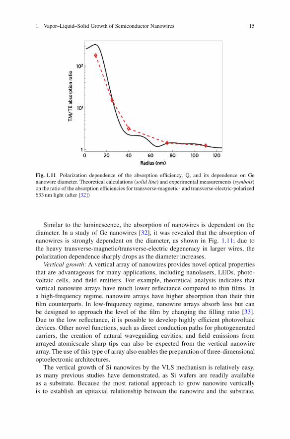
Fig. 1.11 Polarization dependence of the absorption efficiency, Q, and its dependence on Genanowire diameter. Theoretical calculations (solid line) and experimental measurements (symbols)on the ratio of the absorption efficiencies for transverse-magnetic- and transverse-electric-polarized633 nm light (after [32])
Similar to the luminescence, the absorption of nanowires is dependent on thediameter. In a study of Ge nanowires [32], it was revealed that the absorption ofnanowires is strongly dependent on the diameter, as shown in Fig. 1.11; due tothe heavy transverse-magnetic/transverse-electric degeneracy in larger wires, thepolarization dependence sharply drops as the diameter increases.
Vertical growth: A vertical array of nanowires provides novel optical propertiesthat are advantageous for many applications, including nanolasers, LEDs, photo-voltaic cells, and field emitters. For example, theoretical analysis indicates thatvertical nanowire arrays have much lower reflectance compared to thin films. Ina high-frequency regime, nanowire arrays have higher absorption than their thinfilm counterparts. In low-frequency regime, nanowire arrays absorb less but canbe designed to approach the level of the film by changing the filling ratio [33].Due to the low reflectance, it is possible to develop highly efficient photovoltaicdevices. Other novel functions, such as direct conduction paths for photogeneratedcarriers, the creation of natural waveguiding cavities, and field emissions fromarrayed atomicscale sharp tips can also be expected from the vertical nanowirearray. The use of this type of array also enables the preparation of three-dimensionaloptoelectronic architectures.
The vertical growth of Si nanowires by the VLS mechanism is relatively easy,as many previous studies have demonstrated, as Si wafers are readily availableas a substrate. Because the most rational approach to grow nanowire verticallyis to establish an epitaxial relationship between the nanowire and the substrate,

16 H.-J. Choi
Fig. 1.12 SEM images of Mn:Ge nanowires vertically grown on Ge (111) substrate in a (a) 45ı-tilted and (b) cross-section view. The inset of (b), the region indicated by a square in (b), showsthe vertical growth more clearly. (c) HRTEM image of the nanowire grown on Ge (111). SAEDpattern in upper right of (c) confirms that the growth direction of the nanowires is [111] (after [34])
the availability of the same material as the substrate is a great advantage for ahomoepitaxial relationship and vertical growth (refer Figs. 1.7 and 1.9).
Ge nanowires can also be grown vertically with a Ge substrate. For example,Kim et al. successfully grew Ge nanowires vertically on Ge(111) substrates by theVLS mechanism using Au as a catalyst [34]. As shown in Fig. 1.12a, most of theGe nanowires grown on Ge[111] are arrayed vertically. Figure 1.12b and its insetalso show SEM images of vertically grown Ge nanowires in a cross-section view,indicating the epitaxial growth of the nanowires in the [111] direction. In a structuralanalysis using HRTEM and SAED, the SAED pattern confirmed that the single-crystalline nanowires grew in the [111] direction (Fig. 1.12c).
As shown from the growth of Si and Ge nanowires, a homoepitaxial relationshipis a rational approach for the vertical growth of nanowires. Therefore, the best wayto achieve vertical growth of III–V or oxide nanowires is through the respective useof an III–V or oxide substrate. Figure 1.13 shows GaN nanowires grown verticallyon GaN substrates (more precisely, GaN film deposited onto sapphire substrates).This figure indicates that the epitaxial relationship can be a success for the verticalgrowth of III–V nanowires by the VLS mechanism.
It should be noted that such substrates are not available in many cases. Further-more, these types of substrates (e.g, GaN or ZnO) will raise the fabrication cost andthus complicate the mass production of devices. In this regard, the vertical growth

1 Vapor–Liquid–Solid Growth of Semiconductor Nanowires 17
Fig. 1.13 Vertical growth ofGaN nanowires on GaN filmdeposited sapphire substrateby establishing homoepitaxialrelationship betweennanowires and substrate. Thegrowth direction of nanowiresis same as the orientation ofsubstrate, <0001>
of nanowires through a heteroepitaxial relationship between the nanowires andsubstrates has been studied. For example, Kuykendall et al. grew a crystallographicalignment in high-density GaN nanowire arrays using LiAlO2 or MgO [35]. Itwas revealed that the selection of single-crystal substrates is critical for achievingdeterministic control of the growth direction; i.e., a close match of both thesymmetry and lattice constant between the substrate and GaN is essential forsuccessful heteroepitaxy, and this is anticipated to influence the nanowire growthdirection strongly. For example, the oxygen sublattice in the (100) plane of � �LiAlO2 has twofold symmetry, which matches the twofold symmetry of the (100)plane of wurtzite GaN well. The lattice constants a D 5:17 A and c D 6:28 A of��LiAlO2 represent a close match of the lattice constants c D 5:19 A and two timesa D 3:19 A of GaN, respectively. In contrast, the (111) plane of MgO has threefoldsymmetry and an interatomic separation distance of 98 A for atoms in the (111)plane. This is a good match for the threefold symmetry of the (001) plane of GaNand the lattice constant a D 3:19 A. As a result, these two substrates result in theselective growth of GaN nanowires in the [1N10] and [001] directions, respectively.The growth of GaN nanowires vertically on sapphire or Si substrates has also beeninvestigated [36, 37].
Another area of study has been the vertical growth of other III–V groupnanowires, such as GaAs and GaP. The approach for these nanowires is alsobased on the heteroepitaxial relationship. For example, GaP nanowires were grownvertically on Si substrates by utilizing a small lattice mismatch of less than 0.4%relative to Si [38]. It should be noted that epitaxial vertical growth was also achievedin the growth of GaAs nanowires on Si substrates with an interface with a largerlattice mismatch (�4.1%) [39]. A detailed analysis indicated that stacking faults inthe nanowires influence the epitaxial growth of nanowires with a large mismatch.This implies that epitaxial growth can be achieved even under the condition ofa large lattice mismatch between the nanowires and the substrate when a stressmediation mechanism is utilized.
Vertical growth of ZnO nanowires was achieved by utilizing a heteroepitaxialrelationship. For example, ZnO nanowires can be grown vertically on the (110)plane of a sapphire substrate through matching with the (0001) plane of ZnO [40].

18 H.-J. Choi
Fig. 1.14 (a) TEM cross-sectional image of the ZnO nanowires on the GaN substrate. A nearlycontinuous interfacial layer of ZnO separating vertical ZnO nanorods and GaN substrate isindicated using white dashed line. (b) Magnified view of the rectangular area in (a) (after [42])
Though the (110) plane of sapphire is symmetric by twofold and the ZnO c-plane issymmetric by sixfold, the a-axis of ZnO and the c axis of sapphire are mismatchedat less than 0.08%. Such a coincidental matchup along the sapphire [0001]direction leads to the vertical heteroepitaxial growth of ZnO nanowires. Verticallyaligned ZnO nanowires can also be grown on other substrates, for example, GaN,Al0:5Ga0:5N, and AlN substrates [41]. In these substrates, near-perfect verticalalignment of ZnO nanowires was observed, as both ZnO and the substrates havethe same wurtzite structure and because the deposited ZnO nanowires are confinedin their six equivalent < 01N10 > directions and grow along the [0001] direction,following the substrate crystal orientation precisely.
Although a few studies have successfully demonstrated the vertical growth ofIII–V semiconductor and ZnO nanowires, it is also true that the vertical growthof nanowires was found to be unsuccessful in many studies. In those cases, it isunclear whether an epitaxial relationship between the nanowires and substrates wasestablished because an interfacial layer typically formed between the nanowires andthe substrate. These interfacial layers appear to have been deposited by the VSmechanism in advance of the growth of the nanowires by the VLS mechanism.Indeed, closer investigation of the interfaces between the ZnO nanowires andthe GaN substrate showed this type of interface [42] (Fig. 1.14). This issue, theformation and effect of the interfaces, should be addressed in detail to achieve theheteroepitaxial as well as homoepitaxial vertical growth of nanowires.
One of the means of overcoming this difficulty is the activation of a metal catalystfor the VLS mechanism at a low temperature. Figure 1.15 shows the growth of GaNnanowires by the VLS mechanism. The left image shows nanowires grown usingNi as a catalyst. These grew randomly due to the formation of an interfacial layer.However, the right image shows the vertical growth of nanowires when using acocatalyst, e.g., Au–Ni. This cocatalyst creates a liquid alloy at a low temperatureand works as a VLS catalyst in advance of the deposition of the layer by the VSmechanism.
Coaxial heterostructure nanowire (COHN): The optical properties can be manip-ulated by creating COHN. For example, COHN can confine the photons as wellas the electrons and thus yield improved performance of semiconductor lasers andLEDs with a variety of applications that require coherent light sources with low

1 Vapor–Liquid–Solid Growth of Semiconductor Nanowires 19
Fig. 1.15 Vertical growth of GaN nanowires on the GaN deposited sapphire substrate by VLSmechanism using cocatalyst on the substrate
power consumption and the capability of high-speed digital modulation. It is alsoideal for photovoltaic cells due to the large junction area that extends along the entirelength of the nanowire with carrier separation in the radial direction, which promiseshigh efficiency. Furthermore, an electrical injection in COHN can be carried outefficiently with more flexibility in device designs that should be far superior to otherstructures for electrical injection optoelectronics [43].
Based on the VLS mechanism, COHN can be fabricated by two approaches.The first of these involves a combination of the VLS and VS mechanism in whichnanowires using the VLS mechanism are initially grown in the longitudinal direc-tion, after which a shell is deposited in the radial direction by the VS mechanism.A typical example of this approach is GaN/InGaN COHN multiquantum-wellstructures fabricated by the subsequent deposition of an In/AlGaN layer on thesurface of GaN nanowires grown by the VLS mechanism (Fig. 1.16) [44]. Duringthis process, the composition of the shell is controlled by the temperature; amultiquantum-well structure with as many as 26 wells can be fabricated withCOHN.
The other approach to fabricate COHN is through the use of a self-organizationmode in a one-step VLS mechanism. Figure 1.17 shows GaN/AlGaN COHN grownby spontaneous phase separation within the Ga–Al–N alloy nanowire system [45].Bright-field transmission electron microscopy (BFTEM) images of the nanowireshow a “dark” GaN core and a “bright” AlGaN sheath along the axis of nanowireswith smooth surfaces and sharp interfaces. The cores have diameters in the rangeof 5–40 nm, whereas the sheath thickness is in the range of 50–200 nm. The drivingforces for this self-organizing process are the strain that develops in the nanowires.The curved surfaces of the materials are subjected to local pressure �P (and, in turn,stresses) according to the Laplace equation �P D �Œ.1=r1/C.1=r2/�, where r1 andr2 are two principal radii of curvature in a given point of a surface and � is the surfacetension. For nanowires, r1 and r2 correspond to the curvature in the radial andlongitudinal directions, respectively; the former equals the radius of the nanowires,whereas the latter can be assumed to be infinite. Therefore, �P generated on thecurved surface of the nanowires can be estimated as �P D �=rnanowire, wherernanowire is the nanowire radius. Owing to the positive curvature of the surfaces,compressive stresses in the inward radial direction arise and become significant

20 H.-J. Choi
Fig. 1.16 (Left) Strategy for the fabrication of coaxial heterostructure nanowires by longitudinalgrowth by VLS mechanism followed by shell deposition by VS mechanism. A and B componentsare supplied for longitudinal growth and shell deposition, respectively (Right) Structural analysisof In/AlGaN coaxial heterostructure nanowires (after [44])
Fig. 1.17 GaN/AlGaN COHN by self-organization mode. (a) SEM image of nanowires, (b)–(e)TEM images with diffraction pattern, (f) compositional analysis of nanowires (after [45])
as the size decreases. Similar phenomena can be found in the overgrowth ofsemiconductor alloy thin films, where spontaneous phase separation is accompaniedby surface roughening (i.e., the formation of curved surfaces). Such a strain-inducedself-ordering process can also lead to irregular spatial compositional modulation inthe GaInAs nanowire system [46].
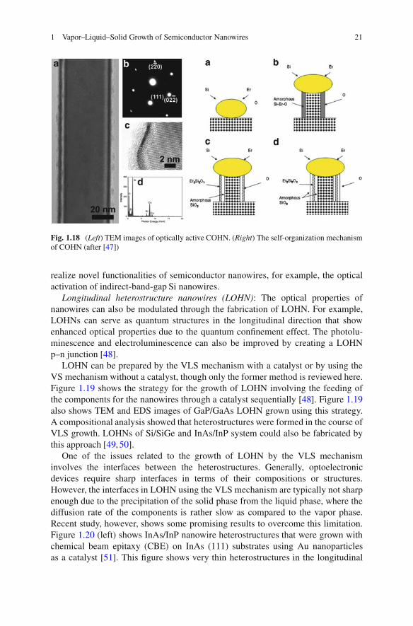
Si COHN can also be prepared in the self-organization mode. Figure 1.18 showsa TEM image of Si–Er COHN and a schematic illustration of the self-organizationprocess for creating single-crystalline Si COHN arrays on (111) Si substrates [47].In this mode, Si and Er are supplied to Au catalysts and form an Au–Si–Er alloy.One-dimensional epitaxial growth of nanowires then occurs with the precipitationof supersaturated Si and Er. Meanwhile, Er is extracted to the outside, where itreacts with oxygen and forms a Si–Er–O amorphous layer. An Er2Si2O7 layer isthen generated on the sheath by phase separation, leaving the amorphous SiO2
layer inside. Further optical characterization showed strong luminescence witha wavelength of 1:54 �m. These outcomes indicate that COHN can be used to
1 Vapor–Liquid–Solid Growth of Semiconductor Nanowires 21
Fig. 1.18 (Left) TEM images of optically active COHN. (Right) The self-organization mechanismof COHN (after [47])
realize novel functionalities of semiconductor nanowires, for example, the opticalactivation of indirect-band-gap Si nanowires.
Longitudinal heterostructure nanowires (LOHN): The optical properties ofnanowires can also be modulated through the fabrication of LOHN. For example,LOHNs can serve as quantum structures in the longitudinal direction that showenhanced optical properties due to the quantum confinement effect. The photolu-minescence and electroluminescence can also be improved by creating a LOHNp–n junction [48].
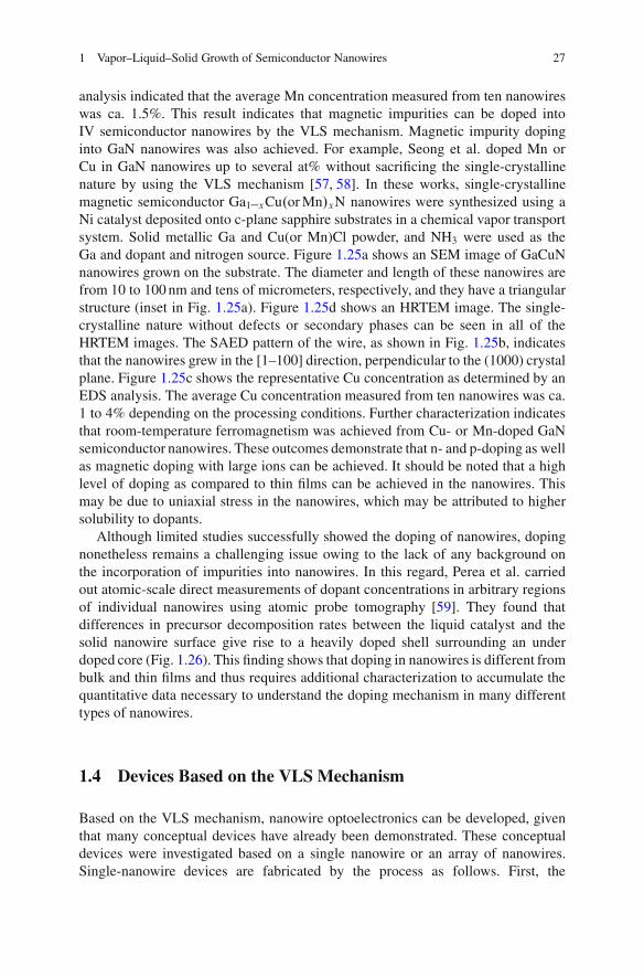
LOHN can be prepared by the VLS mechanism with a catalyst or by using theVS mechanism without a catalyst, though only the former method is reviewed here.Figure 1.19 shows the strategy for the growth of LOHN involving the feeding ofthe components for the nanowires through a catalyst sequentially [48]. Figure 1.19also shows TEM and EDS images of GaP/GaAs LOHN grown using this strategy.A compositional analysis showed that heterostructures were formed in the course ofVLS growth. LOHNs of Si/SiGe and InAs/InP system could also be fabricated bythis approach [49, 50].
One of the issues related to the growth of LOHN by the VLS mechanisminvolves the interfaces between the heterostructures. Generally, optoelectronicdevices require sharp interfaces in terms of their compositions or structures.However, the interfaces in LOHN using the VLS mechanism are typically not sharpenough due to the precipitation of the solid phase from the liquid phase, where thediffusion rate of the components is rather slow as compared to the vapor phase.Recent study, however, shows some promising results to overcome this limitation.Figure 1.20 (left) shows InAs/InP nanowire heterostructures that were grown withchemical beam epitaxy (CBE) on InAs (111) substrates using Au nanoparticlesas a catalyst [51]. This figure shows very thin heterostructures in the longitudinal

22 H.-J. Choi
Fig. 1.19 (Left) Basic approach for the growth of longitudinal heterostructure nanowires usingVLS mechanism. (Right) Compositional analysis of GaP/GaAs longitudinal heterostructurenanowires (after [48])
Fig. 1.20 (Left) TEM imageof InAs/InP longitudinalheterostructure nanowires.(Right) TEM image of InPlongitudinal heterostructurenanowires (after [51, 52])
direction that display a quantum confinement effect. Additionally, sharp interfaceswere achieved by low growth rates together with the rapid switching of an indiumsource (TMIn). These abrupt changes between sections with different compositions,e.g., InAs, InP, or InAsP, along the nanowire with atomically sharp interfacesbetween them are typically challenging to achieve through the liquid phase. It isthus suggested that LOHN with sharp interfaces can be fabricated under controlledconditions.
Additionally, different approaches for the growth of LOHN have been studied[52]. Figure 1.20 (right) shows the InP superlattice of LOHN. To create het-erostructures, InP nanowires were grown first from colloidal gold particles bythe VLS mechanism. In the course of doing this, the nanowires grow in a zinc-blended crystal structure with a supply of diethyl zinc in a vapor form. Whensufficient Zn is supplied, twin planes that exhibit constant spacing for a given Znconcentration and wire diameter appear, with twinning superlattice structures as aresult. These LOHNs form because the doped Zn decreases the activation barrierfor two-dimensional nucleation growth of zinc-blended InP and therefore promotes

1 Vapor–Liquid–Solid Growth of Semiconductor Nanowires 23
the crystallization of the InP nanowires in the zinc-blend instead of the commonlyfound wurtzite crystal structure. It is not clear whether this approach can be appliedto other semiconductor nanowires; however, it deserves further study as a newfabrication means of LOHN with sharp interfaces.
1.3.2.3 Compositional Modulation
Compositional modulation including alloying and doping is essential for the manip-ulation of the optical properties of semiconductors nanowires. For example, thephotoluminescence or electroluminescence from III–V semiconductors can be tunedby modulating the composition in In–Al–Ga–N or In–Al–Ga–As in a quaternary-based system. The absorption of SiGe nanowires can be tuned by the compositionin a binary-based system. This type of compositional modulation is thus importantto exploit the potential of these materials in the area of optoelectronics.
Alloying of nanowires: IV and III–V semiconductors create a complete solidsolution; thus, a binary, ternary, or quarterly alloy (e.g., Si1–xGex; InxGa1–xAs, orAl1–xInyGa1–x–yN) can be prepared. In line with this, compositional modulation ofIV and III–V semiconductor nanowires has been studied.
The alloying of Si nanowires with Ge is readily achieved in the course of growthby the VLS mechanism. For example, Si1–xGex alloy nanowires (x D 0 � 0:3)can be grown on Si (111) substrates using Au as a catalyst and SiCl4 and Gepowders as precursors (Fig. 1.21) [53]. The resulting Si1–xGex nanowires are wellaligned on the substrates, and the diameter of these nanowires typically rangesfrom 50 to 100 nm. The composition of the Si1–xGex nanowires can be varied bychanging the growth temperature or the substrate distance (or both) from the Gepowder, which acts as a Ge precursor. Figure 1.21d shows a typical HRTEM imageof the nanowires. The single-crystalline nature with a thin layer of native oxidecan be seen in the HRTEM image. The SAED pattern recorded along the [001]zone axis, as shown in Fig. 1.21e, indicates that the nanowires grew in the [110]direction. Figure 1.21f shows the relative composition of Si and Ge in the Si1–xGex
nanowires through an EDS analysis, as shown for the Si0:95Ge0:05 and Si0:7Ge0:3
nanowires. This shows the compositional homogeneity of each nanowire with anEDS line scan. The profiles in both the radial and axial directions of the wire showthat the composition of the native oxide is primarily SiOx. No evidence of phaseinhomogeneity was found (Fig. 1.21g, h); that is, no obvious Ge segregation withinthe nanowire was observed, as often found in thin film CVD. These outcomes implythat the alloying of Si and Ge was appropriate, leading to random substitutionalalloy nanowires.
Alloying in III–V semiconductor nanowires is especially important in opto-electronic applications because it creates emissions with various wavelengths,from ultraviolet to the infrared region. Indeed, complete composition tunability ofnanowires in the In–Ga–N system has been achieved [54]. In this study, single-crystalline InxGa1–xN nanowires across the entire compositional range from x D 0
to 1 were grown by low-temperature halide CVD. It also showed tunable emission

24 H.-J. Choi
0 5
GeInte
nsity
(a.
u.)
GeGe
Cu
Si0.7Ge0.3
Si0.95Ge0.05Si
10Photon Energy (keV)
Position (nm)Position (nm)
01401201008060
O O
Ge
Ge
Si Si
402000
500
1000
1500
Inte
nsity
2000
2500
2 nm
(220)
0
1000
2000
Inte
nsity
3000
4000
50 100 150 200 250 300 350
15 20
d
g h
a b c
e f
Fig. 1.21 Si1–xGex nanowires grown by VLS mechanism. SEM images of (a) Si0:95Ge0:05,(b) Si0:85Ge0:15, (c) Si0:7Ge0:3 nanowires aligned on the Si (111) substrates, (d) Typical HRTEMimage of controlled growth Si1–xGex nanowires, showing the single-crystalline and defect-freenature, (e) SAED pattern, taken along the [001] zone axis that confirms the diamond structureof the wire with [110] growth direction, (e) typical EDS spectra of Si0:95Ge0:05 and Si0:7Ge0:3
nanowires. EDS line profiles in both radial (g) and axial (h) directions, showing that compositionof native oxide is primarily SiOx and any evidence of phase inhomogeneity is not found (after [53])
from the near-ultraviolet to the near-infrared region. However, these nanowireswere grown without a catalyst. It should be noted that other studies pertainingto the alloying of III–N nanowires using the VLS mechanism have not beenreported. This may due to the difficulty of alloying of ternary- and quaternary-based systems through a liquid–metal phase. Unlike alloying directly from thevapor phase, the kinetics of alloying through the liquid phase is typically limitedby the thermodynamics and kinetics of the system. However, our recent studydemonstrates that compositional modulation of InGaN nanowires can be achieved

1 Vapor–Liquid–Solid Growth of Semiconductor Nanowires 25
500000cba
300nm 2nm
450000
In8Ga92NIn17Ga83N
In27Ga78N
In40Ga60N
Inte
nsi
ty (
a.u
)
400000
450
Wavelength (nm)
400
Fig. 1.22 InGaN nanowires grown by VLS mechanism and their PL. (a) SEM image of nanowries,(b) TEM image with diffraction pattern, (c) PL of InGaN nanowires with their composition
with the VLS mechanism. Figure 1.22 shows InGaN nanowires grown on a substrateusing a cocatalyst of Au–Ni. The nanowires in this case grew on the substratevertically. Figure 1.22b shows a typical HRTEM image of the nanowires. The single-crystalline nature can be seen in the HRTEM image. The SAED pattern recordedalong the [001] zone axis, as shown in Fig. 1.22b, indicates that the nanowires grewin the [0001] direction. The PL measurements shown in Fig. 1.22c indicate thatcomposition tunability and thus band-gap modulation is feasible through the VLSmechanism.
Alloyed InGaAs nanowires have been demonstrated by the VLS mechanism(Fig. 1.23). Kim et al. grew InGaAs nanowires using the VLS mechanism withAu as a catalyst [55]. Though the composition of these nanowires is not uniformalong the longitudinal direction, their finding clearly indicates that compositionalmodulation can be achieved during the growth process.
Doping of nanowires: To realize electrical injection into a nanowire for opto-electronics, doping of electronic impurities is essential. The functionalizationof nanowires for advanced optics, e.g., realizing magnetism in semiconductornanowires for spin LEDs, also requires functional (e.g., magnetic) impurity doping.
Doping was previously demonstrated in Si nanowires [56]. The process is simpleafter supplying a dopant through vapor with a metal organic CVD precursor or thelaser ablation of a solid target during the course of VLS growth. It results in n- andp-type Si nanowires. In a similar approach, Mg-doped, p-GaN nanowires can beprepared using magnesium nitride (Mg3N2) as a Mg source [37]. In this study, thedoping concentration was controlled by changing the separation distance betweenthe doping source and the substrate (Fig. 1.24, left). As shown in Fig. 1.24 (right),this was effective and changed the resistance of the nanowires.
In addition to electronic impurities, the doping of functional impurities hasbeen studied. One typical example is magnetic impurity doping into semiconductornanowires to realize magnetism in the semiconductor and spin-related optoelectron-ics. Regarding this, Mn was doped into Ge nanowires by transporting germaniumchloride (GeCl4) and manganese dichloride (MnCl2) onto an Au-coated silicon sub-strate [34]. Despite the Mn doping, an analysis revealed that the nanowires maintaintheir single-crystalline nature without defects or secondary phases. Compositional

26 H.-J. Choi
Fig. 1.23 InGaAs nanowires grown by VLS mechanism (after [55])
Fig. 1.24 (Left) Schematic for the apparatus for doping of GaN nanowires. (Right) The resistanceof nanowires as a function of separation between doping source and substrate (after [37])
1 Vapor–Liquid–Solid Growth of Semiconductor Nanowires 27
analysis indicated that the average Mn concentration measured from ten nanowireswas ca. 1.5%. This result indicates that magnetic impurities can be doped intoIV semiconductor nanowires by the VLS mechanism. Magnetic impurity dopinginto GaN nanowires was also achieved. For example, Seong et al. doped Mn orCu in GaN nanowires up to several at% without sacrificing the single-crystallinenature by using the VLS mechanism [57, 58]. In these works, single-crystallinemagnetic semiconductor Ga1–xCu.or Mn/xN nanowires were synthesized using aNi catalyst deposited onto c-plane sapphire substrates in a chemical vapor transportsystem. Solid metallic Ga and Cu(or Mn)Cl powder, and NH3 were used as theGa and dopant and nitrogen source. Figure 1.25a shows an SEM image of GaCuNnanowires grown on the substrate. The diameter and length of these nanowires arefrom 10 to 100 nm and tens of micrometers, respectively, and they have a triangularstructure (inset in Fig. 1.25a). Figure 1.25d shows an HRTEM image. The single-crystalline nature without defects or secondary phases can be seen in all of theHRTEM images. The SAED pattern of the wire, as shown in Fig. 1.25b, indicatesthat the nanowires grew in the [1–100] direction, perpendicular to the (1000) crystalplane. Figure 1.25c shows the representative Cu concentration as determined by anEDS analysis. The average Cu concentration measured from ten nanowires was ca.1 to 4% depending on the processing conditions. Further characterization indicatesthat room-temperature ferromagnetism was achieved from Cu- or Mn-doped GaNsemiconductor nanowires. These outcomes demonstrate that n- and p-doping as wellas magnetic doping with large ions can be achieved. It should be noted that a highlevel of doping as compared to thin films can be achieved in the nanowires. Thismay be due to uniaxial stress in the nanowires, which may be attributed to highersolubility to dopants.
Although limited studies successfully showed the doping of nanowires, dopingnonetheless remains a challenging issue owing to the lack of any background onthe incorporation of impurities into nanowires. In this regard, Perea et al. carriedout atomic-scale direct measurements of dopant concentrations in arbitrary regionsof individual nanowires using atomic probe tomography [59]. They found thatdifferences in precursor decomposition rates between the liquid catalyst and thesolid nanowire surface give rise to a heavily doped shell surrounding an underdoped core (Fig. 1.26). This finding shows that doping in nanowires is different frombulk and thin films and thus requires additional characterization to accumulate thequantitative data necessary to understand the doping mechanism in many differenttypes of nanowires.
1.4 Devices Based on the VLS Mechanism
Based on the VLS mechanism, nanowire optoelectronics can be developed, giventhat many conceptual devices have already been demonstrated. These conceptualdevices were investigated based on a single nanowire or an array of nanowires.Single-nanowire devices are fabricated by the process as follows. First, the

28 H.-J. Choi
Fig. 1.25 Synthesis and structural characterization of Ga1–xCuxN nanowires. (a) Typical SEMimage of Ga1–xCuxN nanowires grown on the sapphire substrate. Inset is TEM image of thenanowire showing a triangular structure. The scale bars in (a) and inset are 5�m and 50 nm,respectively. (b) SAED pattern of the nanowire, recorded on the [0001] zone axis. (c) EDS spectracollected from different positions within the Ga1–xCuxN nanowires as marked with O. Inset isa TEM image of a nanowire. The spectra show essentially the same compositions without anyevidence of phase inhomogeneity. (d) HRTEM image of a nanowire with diameter of 50 nm. Thescale bar is 2 nm (after [58])
Fig. 1.26 Dopantincorporation pathways anddistribution. (a) Schematicrepresentation of dopantincorporation pathways viathe catalyst (i) and surfacedecomposition (ii). (b) Radialplot of phosphorusconcentration for germaniumnanowires. The inset showsthe path along which theconcentration was measured(after [59])
1 Vapor–Liquid–Solid Growth of Semiconductor Nanowires 29
nanowires are grown on the substrate. The nanowires are then dispersed in aliquid medium and assembled ex situ on the substrates, where the electrodes areprepatterned. Fabrication of the top electrodes, serving as a passivation layer,is then carried out to the degree necessary. A typical illustration can be foundin the preparation of InP nanowire optoelectronic devices [60]. In this process,InP nanowires were grown using Au as a catalyst, and Te and Zn were added asprecursors at 1%. After the growth, the nanowires were collected and dispersedin ethanol and then deposited onto oxidized silicon substrates, with conductivesilicon used as a back gate. Electrical contact for the NWs was done using electronbeam lithography. Ni/In/Au contact electrodes were then thermally evaporated. Bythis process, a single-nanowire device can be fabricated. Moreover, to fabricatecross-nanowires as a junction structure, layer-by-layer deposition was used. Inthis process, first a dilute solution of one type of nanowire is deposited on thesubstrate and the positions of individual nanowires are recorded. In the second step,a dilute solution of another type (for example, p-type) of nanowires is deposited, andthe positions of the crossed n- and p-type nanowires are recorded. Metal electrodesare then defined. The inset in Fig. 1.27b shows the crossed nanowire p–n junction,while Fig. 1.27 shows an optical image of the electroluminescence characteristicsof the junction.
By further modulating the nanowires during the course of their growth, moreversatile devices can be fabricated. One example is the multicolor emission of ananowire LED [61]. Figure 1.28a shows the concept of single-nanowire structuresthat consist of an inner n-type GaN core and sequentially deposited i-InGaN,i-GaN, p-AlGaN, and p-type GaN shells for modulation of the luminescence. In thisstructure, the n-type GaN core and the p-type GaN outer shell serve as electron andhole injection layers, respectively. The InxGa1–xN layer provides a tunable band gapas well for the efficient radiative recombination of injected carriers, while the widerband gap and lower index of refraction of the AlGaN cladding layer can enhancethe confinement of both carriers and photons in the InGaN active layer. Based onthis concept, n � GaN=InxGa1–xN=GaN=p � AlGaN=p � GaN nanowire radialheterostructures were grown by longitudinal growth using a catalyst followed bycontrolled shell deposition onto the nanowire core. During the deposition process,the composition of the InGaN layer was systematically tuned and could therefore beused to define the band gap of the InGaN and the corresponding emission energy.Through these modulations, the nanowire devices yielded electroluminescence (EL)with red shifts in their emission peak after increasing the In composition with highquantum efficiency. This approach was also used for the growth of a single COHNfor photovoltaic cells [62].
Nanowire array optoelectronic devices were fabricated in an in situ mode usingthe as-grown nanowires on the substrates. Figure 1.29 shows the typical processof the fabrication of a nanowire array for optoelectronics, such as LEDs [57]. Theprocess starts with the growth of the nanowires on the substrates. In this step, thenanowires can be modulated structurally (e.g., diameter control) or compositionally(e.g., doping of electronic or magnetic impurities) to improve the performance ofthe device. In the example in Fig. 1.29, quasivertically aligned GaN nanowires

30 H.-J. Choi
Fig. 1.27 Optoelectrical characterization of nanowire p–n junctions. (a) Electroluminescence(EL) image of the light emitted from a nanowire p–n junction. Inset: photoluminescence (PL)image of the junction, (b) EL intensity versus voltage. Inset: I ˙V characteristics, (c) EL spectrumof the junction shown in (a), (d) EL spectrum recorded from a second forward-biased crossednanowire p–n junction. Inset: EL image showing that the EL originates from the junction region(after [60])
were grown on n-SiC (0001) substrates using Ni catalysts (Fig. 1.29a). Here, ann-SiC substrate was used to construct a p–n junction between the nanowires and thesubstrates and also for the alignment of the GaN nanowires. During the growthprocess, the nanowires were compositionally modulated by doping with Mn toachieve magnetism as well as p-type characteristics. Therefore, the p–n junctionsformed at the interface between the nanowires and the substrates while the diameterand length were controlled by the thickness of the Ni films and the growth time.The fabrication of electrodes on top of the nanowires and on the bottom of thesubstrates for electrical injections was done subsequent to the growth process. Inthis case, ohmic contacts were achieved by evaporating Ni/Au and Ni bilayers onthe nanowires and substrates, respectively, followed by rapid thermal annealing.Transport measurements showed well-defined current rectification characteristic ofp–n diodes (Fig. 1.29c). The I –V data recorded from the nanowires and substratewere symmetric and thus can attribute the rectification to the p–n junction betweenthe nanowires and substrate and not to the junction between the nanowires and

1 Vapor–Liquid–Solid Growth of Semiconductor Nanowires 31
Fig. 1.28 (Left) Cross-sectional view of a nanowire heterostructure and the corresponding energyband diagram. (Right) (a) Current versus voltage data recorded on a nanowire device. Inset: fieldemission scanning electron microscopy image of a representative nanowire device. (b) Opticalmicroscopy images collected from around p-contact of nanowire LEDs in forward bias, showingpurple, blue, greenish-blue, green, and yellow emission, respectively. (c) Normalized EL spectrarecorded from five representative forward-biased multicolor nanowire LEDs (after [61])
the metal contacts. Electroluminescence spectra measurements of these junctionsshowed a dominant emission peak centered at 430 nm, which is consistent with thePL of the nanowires (Fig. 1.29e).
A good example that shows a combination of the CMOS process with thestructural and compositional modulation of nanowires for realizing nanowire-basedLEDs is contained in the report by Sevenson et al. [63] (Fig. 1.30). In this work,i-GaAs nanowires were grown on a p-Si/p-GaP substrate vertically by the VLSmechanism using Au as catalyst. The GaAs nanowires were grown vertically on theGaP and Si substrates due to the epitaxial relationship between the nanowires andthe substrates (Fig. 1.31). For the positioning of the nanowires, standard lithographytechniques were used. After the growth of the nanowires, InGaP shells with n-typedoping were deposited on the surface of the nanowires and p–i–n junction structureswere then formed in the nanowires. The fabrication of the electrodes was donevia a standard CMOS process. The established LED functionality of these devicesdemonstrated that modulation of nanowires by the VLS mechanism can be carriedout in the CMOS process for advanced optoelectronics.
Other optoelectronic devices can be developed based on the VLS mechanism.For example, the growth of III–V nanowires on Si has also been demonstrated forthe fabrication of GaN nanowire-based solar cells. In this study, vertically alignedMg-doped GaN nanorods were epitaxially grown on an n-type Si substrate. Theresult showed a good high-photocurrent density, high-energy conversion efficiency,

32 H.-J. Choi
Wavelength (nm)
5004003000.0
0.2
0.4
0.6
0.8
1.0e
c
a b
d
2.9 eV
PL
lnte
nsity
(A
.U.)
EL
lnte
nsity
(A
.U.)
2.35 eV
Bias Voltage (V)
–10 –8 –6 –4 –2 0 2 4 6 8 10–0.001
0.000
Cur
rent
(A
)
0.001
0.002
0.0034H-SiC WaferIndividual GaN:Mn NW4H-SiC/GaN:Mn NWs
current/10
current × 100
10 mm
NI/Au
Nl
Mn:GaN NWs
n-type SiC
TaOx
600 700 800 900
Fig. 1.29 GaN:Mn nanowire LED. (a) SEM image of the quasivertical nanowire arrays onsubstrate, (b) schematic illustration of the LED structures, (c) I –V behavior of n-SiC substrate/GaN:Mn nanowire junction, (d) image of light-emitting interface. Top and bottom images showthe device configuration of the nanowire-based LED structure and an optical image of the emittingdevice, respectively, (e) EL spectrum from nanowire LED, and PL spectrum from GaN:Mnnanowires measured at room temperature using He–Cd laser as excitation source (after [57])
and reduced light loss due to reflection [64]. Though the interfaces were not clearlycharacterized, this outcome also demonstrates that vertically aligned nanowire p–njunctions can be fabricated by the VLS mechanism. A Si nanowire-based photode-tector has also been investigated similarly through the growth of Si nanowires on asubstrate, and a photodetector was fabricated in a manner similar to that used withLED or photovoltaic cells [65].

1 Vapor–Liquid–Solid Growth of Semiconductor Nanowires 33
1.5 Summary and Perspectives
The VLS mechanism has been successfully used for the growth of nanowires foroptoelectronics. The uniqueness that has made this mechanism a mainstay for thegrowth of nanowires is its simplicity. The VLS mechanism can be realized by simplyadding a metal catalyst to the crystal growth process. Therefore, it can be easilyadapted in many conventional semiconductor fabrication processes. Because thismechanism has been rediscovered for the growth of nanowires, most of the studiesrelated to it have investigated metal catalysts to the point that this mechanism is nowconsidered a general method that can be used for the growth of various nanowires.The feasibility of the structural and compositional modulation of nanowires furtherfuels this mechanism as workhorse in this field.
However, it is true that several issues have to be addressed before the potentialof the VLS mechanism can be exploited in the future. One of these issues is theestablishment of the nanothermodynamics and kinetics for the nanoliquid–solidsystem. The thermodynamic and kinetic data from bulk materials have been usedto explain the growth of nanowires thus far. However, the growth that occurs innanosystems in which the thermodynamics and kinetics are different is itself quitedifferent to that in bulk systems. Therefore, frameworks such as size effect on thephase relationship, role of surface energy on the stability of 1 D nanostructures,and diffusion kinetics in liquid on a nanometer scale have to be established. Suchfundamentals are essential to grow nanowires rationally. It can also pave the wayfor the preparation of nanowires in an unprecedented size range of sub-10 nm.The compatibility of metal catalysts to the CMOS process should be addressed fordevice fabrication. Though nanowires can be grown easily with a metal catalystin a semiconductor fabrication process, some of them are not compatible with theCMOS process. The possible unintended contamination of a catalyst componentin nanowires should also be addressed. A few studies have been done on thisissue; however, more quantitative data have to be published to overcome this issue
Fig. 1.30 Side-view scanning electron microscopy (SEM) image showing nanowire LEDs. Leftinset: sketch drawing of the device structure. Right inset: side-view CCD camera image showingelectroluminescence (EL) from a single-nanowire LED structure (after [63])

34 H.-J. Choi
Fig. 1.31 (a) Tilt top view SEM image of Mg-doped GaN nanorod arrays. Inset shows cross-sectional SEM image. (b) HRTEM image of GaN nanorod and its corresponding SAED pattern(inset). (c) AFM image of GaN nanorod tips exposed above the photoresist layer. (d) A schematicof the p-GaN nanorod/n-Si heterojunction photovoltaic cell (after [64])
and in turn to achieve the better optical properties of nanowires. Regarding these,the correlation of the final optical properties with the structure and compositionof nanowires may reveal the more sensitive processing parameters for the VLSmechanism. These parameters can be studied quantitatively as well as qualitativelyto establish the growth process of nanowires in a predictable, reliable manner foroptoelectronic applications. The scaling up of the growth process is another issuethat should be addressed. This issue has not been investigated thoroughly as yet;however, this will be important for the industrialization of nanowires near future.To achieve this, the many steps required for the growth of nanowires should bestandardized to achieve reliability of the growth process.
Since the 1990s, the VLS mechanism has played a critical role in the creationof the science of nanowires, which has fueled the advance in many optoelectronicfields. The many studies carried over the past two decades have built the foundationof the great potential of this mechanism. To step forward in this area, the mechanismhas to be developed from the point of view of industrialization of the nanowires. Itwill fuel the scientific research in the field of nanowires as well as the creation ofadvanced optoelectonic market.
Acknowledgements This work was supported by a grant from the National Research Laboratoryprogram and Pioneer Program through the Korea Science and Engineering Foundation funded bythe Ministry of Education, Science & Technology.

1 Vapor–Liquid–Solid Growth of Semiconductor Nanowires 35
References
1. S. Wagner, W.C. Ellis, Appl. Phys. Lett. 4, 89 (1964); in Whisker Technology. ed. by A.P. Levitt(John Wiley and Sons, Inc., New York, 1970)
2. H.-J. Choi, J.-G. Lee, J. Mat. Sci. 30, 1982 (1995)3. Y. Wu, P. Yang, J. Am. Chem. Soc. 123, 3165 (2001)4. F.M. Ross, J. Tersoff, M.C. Reuter, Phys. Rev. Lett. 95, 146104 (2005)5. V. Schmidt, J.V. Wittemann, S. Senz, U. Gosele, Adv. Mat. 21, 2681 (2009)6. T.B. Massalski, P.R. Submanian, H. Okamoto, Binary Alloy Phase Diagrams, 2nd ed., vol. 1
(ASM International, Materials Park, OH, 1998)7. E.A. Sutter, P.W. Sutter, ACS Nano 4, 4943 (2010)8. H. Adhikari, A.F. Marshall, I.A. Goldthorpe, C.E.D. Chidsey, P.C. McIntyre, ACS Nano 1, 415
(2007)9. E.J. Schwalbach, P.W. Voorhees, Nano Lett. 8, 3739 (2008)
10. S. Kodambaka, J. Tersoff, M.C. Reuter, F.M. Ross, Science 316, 729 (2007)11. E.I. Givargozov, J. Cryst. Growth 31, 20 (1975)12. T.I. Kamins, R.S. Williams, D.P. Basile, T. Hesjedal, J.S. Harris, J. Appl. Phys. 89, 1008
(2001)13. K. Lew, J.M. Redwing, J. Cryst. Growth 254, 14 (2003)14. J. Kikkawa, Y. Ohno, S. Takeda, Appl. Phys. Lett. 86, 123109–1 (2005)15. M.H. Huang, Y.Wu, H. Feick, N. Tran, E. Weber, P. Yang, Adv. Mat. 13, 113 (2001)16. H. Jeong, T.E. Park, H.K. Seong, M. Kim, U. Kim, H.J. Choi, Chem. Phys. Lett.467, 331
(2009)17. T. Stelzner, G. Andra, E. Wendler, W. Wesch, R. Scholz, U. Gosele, S. Christiansen, Nano-
technology 17, 2895 (2006)18. J.E. Allen, E.R. Hemesath, D.E. Perea, J.L. Lenscch-Falk, Z.Y. Li, F. Yin, M.H. Gass, P. Wang,
A.L. Bleloch, R.E. Palmer, L.J. Lauhon, Nat. Nanotechnol., 3, 168. (2008)19. J.B. Hannon, S. Kodambaka, F.M. Rossand, R.M. Tromp, Nature 440, 69 (2006)20. Y. Ke, X. Weng, J.M. Redwing, C.M. Eichfeld, T.R. Swisher, S.E. Mohney, Y.M. Habib, Nano
Lett. 9, 4494 (2009)21. Y. Wang, V. Schmidt, S. Senz, U. Gosele, Nat. Nanotechnol. 1, 186 (2006)22. P.X. Gao, Y. Ding, Z.L. Wang, Nano Lett. 3, 1315 (2003)23. J. Yoo, Y.-J. Hong, S. An, G.-C. Yi, B. Chon, T. Joo, J.-W. Kim, J.-S. Lee, Appl. Phys. Lett.
89, 043124–1 (2006)24. B. Mandl, J. Stangl, E. Hilner, A.A. Zakharov, K. Hillerich, A.W. Dey, L. Samuelson, G. Bauer,
K. Deppert, A. Mikkelsen, Nano Lett. 10, 4443 (2010)25. L. Gao, R.L. Woo, B. Liang, M. Pozuelo, S. Prikhodko, M. Jackson, N. Goel, M.K. Hudait,
D.L. Huffaker, M.S. Goorsky, S. Kodambaka, R.F. Hicks, Nano Lett. 9, 2223 (2009)26. B. Delleyand, E.F. Steigmeier, Appl. Phys. Lett. 67, 2370 (1995)27. C. Harris, E.P. O’Reilly, Physica E 32, 341 (2006)28. Y. Wu, Y. Cui, L. Huynh, C.J. Barrelet, D.C. Bell, C.M. Lieber, Nano Lett. 4, 433 (2004)29. J. Goldberger, R. He, Y. Zhang, S. Lee, H. Yan, H.-J. Choi, P. Yang, Nature 422, 599 (2003)30. M.S. Gudiksen, J. Wang, C.M. Lieber, J. Phys. Chem. B 106, 4036 (2002)31. X. Wang, Y. Ding, C.J. Summers, Z.L. Wang, J. Phys. Chem. B 108, 8773 (2004)32. L. Cao, J.S. White, J.-S. Park, J.A. Schuller, B.M. Clemens, M.L. Brongersma, Nat. Mater. 8,
643 (2009)33. L. Hu, G. Chen, Nano Lett. 7, 3249 (2007)34. U. Kim, T.-E. Park, I. Kim, H.-K. Seong, M.-H. Kim, J. Chang, J.-G. Park, H.-J. Choi, J. Appl.
Phys. 106, 123903–1 (2009)35. T. Kuykendall, P.J. Pauzauskie, Y. Zhang, J. Goldberger, D. Sirbuly, J. Denlinger, P. Yang, Nat.
Mater. 3, 524 (2004)36. Y.B. Tang, Z.H. Chen, H.S. Song, C.S. Lee, H.T. Cong, H.M. Cheng, W.J. Zhang, I. Bello,
S.T. Lee, Nano Lett. 8, 4191 (2008)

36 H.-J. Choi
37. Z. Zhong, F. Qian, D. Wang, C.M. Lieber,Nano Lett. 3, 343 (2003)38. T. Martensson, C.P.T. Svensson, B.A. Wacaser, M.W. Larsson, W. Seifert, K. Deppert,
A. Gustafsson, L.R. Wallenberg, L. Samuelson, Nano Lett. 4, 1987 (2004)39. X.-Y. Bao, C. Soci, D. Susac, J. Bratvold, D.P.R. Aplin, W. Wei, C.-Y. Chen, S.A. Dayeh, K.L.
Kavanagh, D. Wang, Nano Lett. 8, 3755 (2008)40. M.H. Huang, S. Mao, H. Feick, H. Yan, Y. Wu, H. Kind, E. Weber, R. Russo, P. Yang, Science
292, 1897 (2001)41. X. Wang, J. Song, P. Li, J.H. Ryou, R.D. Dupuis, C.J. Summers, Z.L. Wang, J. Am. Chem.
Soc. 127, 7920 (2005)42. I. Levin, A. Davydov, B. Nikoobakht, N. Sanford, P. Mogilevsky, Appl. Phys. Lett. 87, 103110–
1 (2005)43. D. Li, C.Z. Ning, Nano Lett. 8, 4234 (2008)44. F. Qian, Y. Li, S. Gradecak, H. Park, Y. Dong, Y. Ding, Z. Wang, C.M. Lieber, Nat. Mater. 7,
791 (2008)45. H.-J. Choi, J.C. Johnson, R. He, S.-K. Lee, F. Kim, P. Pauzauskie, J. Goldberger, R.J. Saykally,
P. Yang, J. Phys. Chem. B, 107, 8721 (2003)46. P.D. Markowitz, M.P. Zach, P.C. Gibbons, R.M. Penner, W.E. Buhro, J. Am. Chem. Soc. 123,
4502 (2001)47. H.-J. Choi, J.H. Shin, K. Suh, H.-K. Seong, H.-C. Han, J.-C. Lee, Nano Lett. 5, 2432(2005)48. M.S. Gudiksen, L.J. Lauhon, J. Wang, D.C. Smith, C.M. Lieber, Nature 415, 617 (2002)49. M.T. Bjork, B.J. Ohlsson, T. Sass, A.I. Persson, C. Thelander, M.H. Magnusson, K. Deppert,
L.R. Wallenberg, L. Samuelson, Nano Lett. 2, 87 (2002)50. Y. Wu, R. Fan, Peidong Yang, Nano Lett., 2, 83 (2002)51. A. Fuhrer, L.E. Froberg, J.N. Pedersen, M.W. Larsson, A. Wacker, M.-E. Pistol, L. Samuelson,
Nano Lett.7, 243 (2007)52. R.E. Algra, M.A. Verheijen, M.T. Borgstrom, L. Feiner, G. Immink, W.J.P. VanEnckevort,
E. Vlie, E.P.A.M. Bakkers, Nature, 456, 369–372 (2008)53. H.-K. Seong, E.-K. Jeon, M.-H. Kim, H. Oh, J. Lee, J.-J. Kim, H.-J. Choi, Nano Lett. 8, 3656
(2008)54. T. Kuykendall, P. Uurich, S. Aloni, P. Yang, Nat. Mater. 6, 951 (2007)55. Y. Kim, H.J. Joyce, Q. Gao, H.H. Tan, C. Jagadish, M. Paladugu, J. Zou, A.A. Suvorova, Nano
Lett. 6, 599 (2006)56. Y. Cui, X. Duan, J. Hu, C.M. Lieber, J. Phys. Chem. B 104, 5213 (2000)57. H.-J. Choi, H.-K. Seong, J. Chang, K.-I. Lee, Y.-J. Park, J.-J. Kim, S.-K. Lee, R. He,
T. Kuykendall, Peidong Yang, Adv. Mater. 17, 1351 (2005)58. H.-K. Seong, J.-Y. Kim, J.-J. Kim, S.-C. Lee, S.-R. Kim, U. Kim, T.-E. Park, H.-J. Choi, Nano
Lett. 7, 3366 (2007)59. D.E. Perea, E.R. Hemesath, E.J. Schwalbach, J.L. Lensch-Falk, P.W. Voorhees, L.J. Lauhon,
Nat. Nanotechnol. 4, 315 (2009)60. X. Duan, Y. Huang, Y. Cui, J. Wang, C.M. Lieber, Nature 409, 66 (2001)61. F. Qian, S. Gradecak, Y. Li, C.-Y. Wen, C.M. Lieber, Nano Lett. 5, 2287 (2005)62. Y. Dong, B. Tian, T.J. Kempa, C.M. Lieber, Nano Lett. 9, 2183 (2009)63. C.P.T. Svensson, T. Martensson, J. Tragardh, C. Larsson, M. Rask, D. Hessman, L. Samuelson,
J. Ohlsson, Nanotechnology 19, 305201 (2008)64. Y.B. Tang, Z.H. Chen, H.S. Song, C.S. Lee, H.T. Cong, H.M. Cheng, W.J. Zhang, I. Bello,
S.T. Lee, Nano Lett. 8, 4191 (2008)65. J. Bae, H. Kim, X.-M. Zhang, C.H Dang, Y. Zhang, Y.J. Choi, A. Nurmikko, Z.L Wang,
Nanotechnology 21, 095502 (2010)

http://www.springer.com/978-3-642-22479-9