utdsp: a vliw dsp processor in tsmc 0.35 cmosspeng/thesis/texpo99_peng_tr.… · · 2000-02-04in...
TRANSCRIPT

UTDSP: A VLIW DSP Processor in TSMC 0.35 CMOS
Sean Hsien-en PengSupervisor: Prof. Paul Chow
Computer Engineering GroupUniversity of Toronto
Copyright@1999 by Sean Peng

• Motivation • Low-Cost, Low-Power and High-
Performance DSP Processors are needed for telecommunication and embedded systems
• VLIW architectures are ideal targets for HLL compilers to exploite parallelism Flexible for application-specific embedded
systems( Current VLIWs: TI TMS320C6x, and Philips
R.E.A.L. DSP )
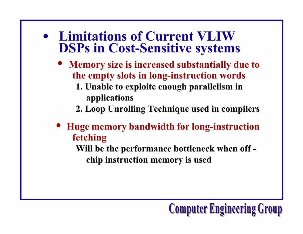
• Limitations of Current VLIW DSPs in Cost-Sensitive systems
• Memory size is increased substantially due to the empty slots in long-instruction words1. Unable to exploite enough parallelism in
applications2. Loop Unrolling Technique used in compilers
• Huge memory bandwidth for long-instruction fetchingWill be the performance bottleneck when off -
chip instruction memory is used

• The New TI VelociTI Architecture in TMS320C6x

• A Novel Instruction Packing and Decoding Method
• Based on a two-level horizontal microcode architecure
• Achieve better packing results while eliminating the need of using crossbar
• Reduce off-chip instruction memory bandwidth for cost-sensitive systems
• Patent has been filed for the memory packing design

• The UTDSP Memory System

• Reduce size of Decoder Memory
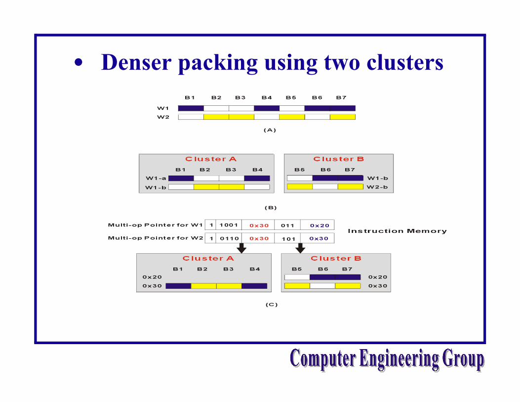
• Denser packing using two clusters

• Combine clusters and slot sharing to have a near-optimal result

• The Packer and Software tools
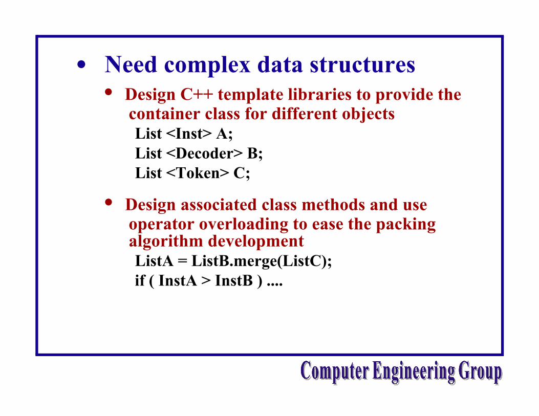
• Need complex data structures • Design C++ template libraries to provide the
container class for different objectsList <Inst> A;List <Decoder> B;List <Token> C;
• Design associated class methods and use operator overloading to ease the packing algorithm developmentListA = ListB.merge(ListC);if ( InstA > InstB ) ....

• Better VLIW solution than TI’s new VelociTI architecture
• Similar instruction compaction rate (65%)
• Eliminate the necessity of using crossbar
• Can use inexpensive off-chip instruction memory without suffering the bandwidth problem that TI has.
• Minimize the size of on-chip memory90% of execution time is spent in 10% of code=> only need to store DSP kernel code on chip

• The UTDSP Architecture

• Instruction Set • Highly orthogonal, RISC-like instructions
add r1,r2,r3, mult r1,r2,r3, ld (a1), r2 st r4,(a5)JSR, Jmp, BEQ, BLE.
• Specialized DSP instructions multiply-accumulator, modulo addressing,
• Zero-Overhead Looping InstructionAchieve optimal performance in DSP kernelsCan handle 8-level nested looping, interruptable, good for real-time application

• Data Hazards and Data Forward • Traditional RISC architectures stall pipelines
to solve RAW data hazards
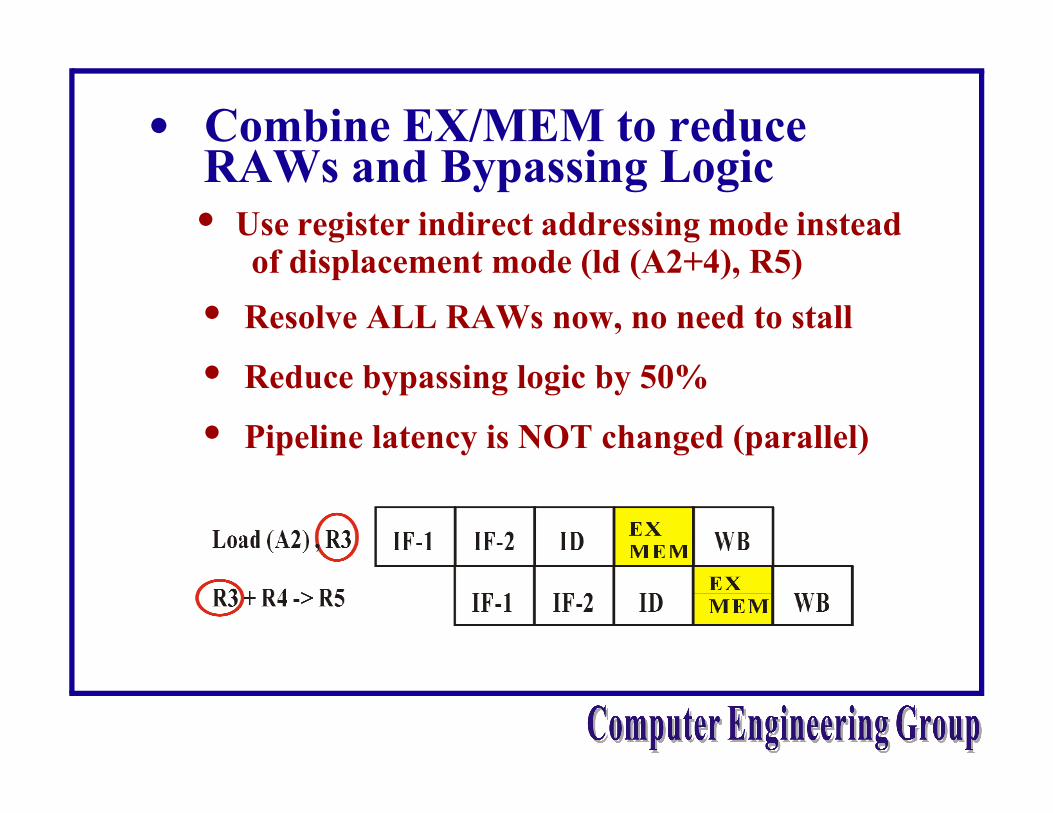
• Combine EX/MEM to reduce RAWs and Bypassing Logic
• Use register indirect addressing mode instead of displacement mode (ld (A2+4), R5)
• Resolve ALL RAWs now, no need to stall
• Reduce bypassing logic by 50%
• Pipeline latency is NOT changed (parallel)

• Zero-overhead Looping Inst. reduces branch penalty and size of instruction memory
• TI suggests assembly programmers using Loop Unrolling to optimize DSP kernel code1. Difficult 2. Increase code size dramatically
• UTDSP has a zero-overhead DO instruction

• Design Challenge: The PC Unit: Handles 8-level nested DO loop. Allows JSR, Branch, and Interrupts in inner loop

• The Forwarding Logic:

• VLSI Implementation Strategy • “P&R a subblock and instantiate it at top-
level” methodology doesn’t work in processor design
• Various size of blocks => Need grouping/merging features in floorplan tools
• Memory blocks => Need hierarchical P&R
• Huge interconnection bandwidth between blocks (bypassing) => Need Global Pin Optimization (GPO)
• 0.35u: Wiring delay dominates gate delay => Need GPO and Area-based router


• Benchmark Results
UTDSP Quick Facts: Die size: 7.2 x 7.2 mm 170,000 gates 20KByte On-chip SRAM
Texas Instruments TMS320C62
Philips R.E.A.L DSP (Core)
The UTDSP
Clock 200 MHz 70 MHz 70 MHz
Pin count > 400 pins 105 pins
Func. Units 8 10 7
FIR 4, N_coeff, M_output smaples
Mx( N+8)/2 + 6 cycles
~Mx(N+7)/2 + 8 clcles
M x (N+6) /2 + 6 cycles

• S.O.C Solution for Low-Cost Low-Power Telecommunication and Consumer applications
• The UTDSP core implemented in synthesizable VHDL can be easily integrated with other system blocks as an IP core
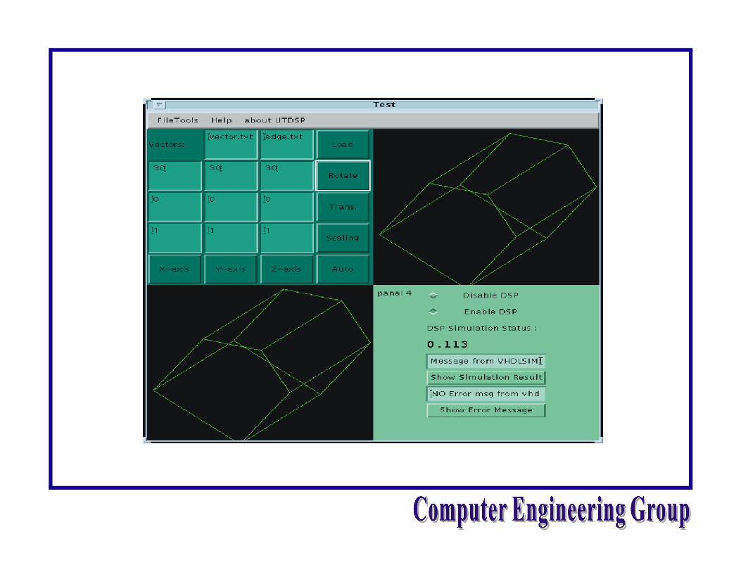
• Provide a GUI-based architecture simulator to help desingers to evaluate/modify the UTDSP core
• Provide an interactive assembly debugger comparable to any commercial counterpartsSingle-step trace, set break-point, memory
location probing.
• Conclusion: What has been done • RTL level VHDL for UTDSP (10,000 lines)
• UTDSP Long-instruction packer and assembler ( 5,000 line C++ with template)
• Hierarchical P&R flow using PDP + Silicon Ensemble + Cadence 1999a
• GUI-based assembly debugger and simulator (6,000 lines in Java )
• Potential commercialization will benefit the Canadian industry

The Assembly Debugger

Before Logic Merging: (Cadence PDP3.4C)

After Logic Merging: (Cadence PDP3.4C )

Global Pin Optimization (Cadence PDP 3.4C )
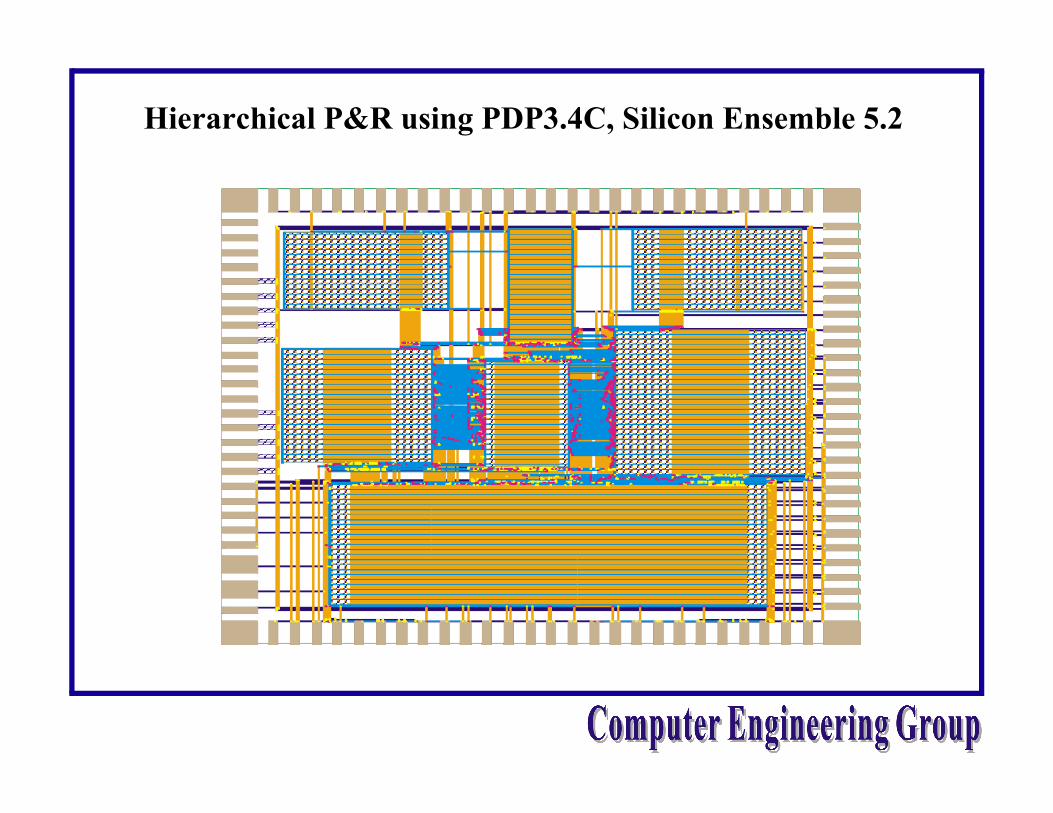
Hierarchical P&R using PDP3.4C, Silicon Ensemble 5.2

Finalized Grouping and Floorplan
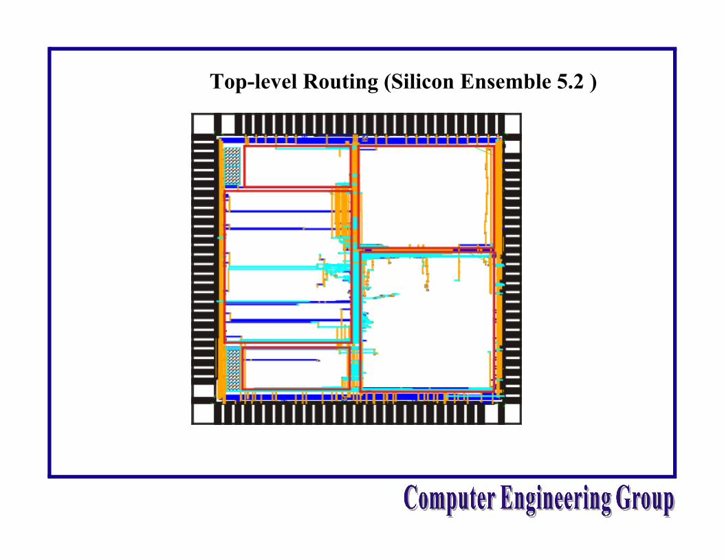
Top-level Routing (Silicon Ensemble 5.2 )

• Java-HDL System ( Experimental, Not shown in TEXPO99 )
• Use Java language to describe digital design
• Embedd timing info into wires, and ports so that wire delay can be estimated in early design stage.
• Schematic is automatically generated and is used for visualized simulation => Important for DSP ASIC or pipelined
design. You can observe any internal wires without using waveform simulator
• Synthesizable VHDL is automatically created

• Java-HDL code example: public class Register ... { Inport p1; Inport p2; ... Wire w5 = new Wire(4); // a 4-bit wide bus Wire w6 = new Wire(1); // one -bit .. if ( rst.value == 1 ) w8.drive(0); else if ( event1(clk) ) w8.drive(D); .

Java-HDL Simulation System