utc2000 data sheet - microchip technologyww1.microchip.com/downloads/en/devicedoc/utc2000 ds...
TRANSCRIPT

UTC2000Basic USB Type-CTM Controller
Highlights
• Transition any existing USB Type-A design to a USB Type-CTM Downstream Facing Port or any existing Type-B design to a USB Type-C Upstream Facing Port
• Leverage the USB Type-C reversible cable and compact form factor
• For use with USB 2.0, USB 3.0 or USB 3.1
• Supports legacy, 1.5A, & 3.0A USB Type-C charging profiles
• Compact 3 x 3mm 16-pin QFN package
• Commercial, industrial, and automotive extended temperature support
• Requires minimal design effort
Target Applications
• Laptops
• Desktop PCs
• Monitors
• USB Hubs
• USB Wall Chargers
• Industrial
• Automotive
Key Benefits
• USB Type-C cable connection and orientation detection
• Orientation detection indicator for optional USB switch control
• Powered cable detection with VCONN powered cable supply control
• CFG_SEL pin configurable charging profiles:
- 5V Legacy DFP mode (500mA for USB 2.0, 900mA for USB 3.0/USB 3.1)
- 5V @ 1.5A DFP mode
- 5V @ 3.0A DFP mode
- UFP mode
• ENABLE pin for host/hub port control
• VMON pin monitors VBUS overvoltage conditions
• USB Type-C Audio Adapter detection and control
• OCS# fault input pin
• FAULT_IND fault indicator output pin
• Operating Voltage Range:
- 4.5V to 5.5V
• Package
- 16-pin QFN (3 x 3 x 0.9mm)
• Environmental
- Commercial temperature range(0°C to +70°C)
- Industrial temperature range(-40°C to +85°C)
- Extended temperature range(-40°C to +125°C)
2015 Microchip Technology Inc. DS00001957C-page 1

UTC2000
TO OUR VALUED CUSTOMERS
It is our intention to provide our valued customers with the best documentation possible to ensure successful use ofyour Microchip products. To this end, we will continue to improve our publications to better suit your needs. Our pub-lications will be refined and enhanced as new volumes and updates are introduced.
If you have any questions or comments regarding this publication, please contact the Marketing CommunicationsDepartment via E-mail at [email protected] or fax the Reader Response Form in the back of this datasheet to (480) 792-4150. We welcome your feedback.
Most Current Data Sheet
To obtain the most up-to-date version of this data sheet, please register at our Worldwide Web site at:
http://www.microchip.com
You can determine the version of a data sheet by examining its literature number found on the bottom outside cornerof any page. The last character of the literature number is the version number, (e.g., DS30000A is version A of docu-ment DS30000).
Errata
An errata sheet, describing minor operational differences from the data sheet and recommended workarounds, mayexist for current devices. As device/documentation issues become known to us, we will publish an errata sheet. Theerrata will specify the revision of silicon and revision of document to which it applies.
To determine if an errata sheet exists for a particular device, please check with one of the following:
• Microchip’s Worldwide Web site; http://www.microchip.com
• Your local Microchip sales office (see last page)
When contacting a sales office, please specify which device, revision of silicon and data sheet (include literature num-ber) you are using.
Customer Notification System
Register on our web site at www.microchip.com to receive the most current information on all of our products.
DS00001957C-page 2 2015 Microchip Technology Inc.

2015 Microchip Technology Inc. DS00001957C-page 3
UTC2000
Table of Contents
1.0 Introduction ..................................................................................................................................................................................... 42.0 Pin Descriptions .............................................................................................................................................................................. 73.0 Functional Description .................................................................................................................................................................. 114.0 Operational Characteristics ........................................................................................................................................................... 195.0 UTC2000 System Application ....................................................................................................................................................... 236.0 Packaging Information .................................................................................................................................................................. 33Appendix A: Data Sheet Revision History ........................................................................................................................................... 37The Microchip Web Site ...................................................................................................................................................................... 39Customer Change Notification Service ............................................................................................................................................... 39Customer Support ............................................................................................................................................................................... 39Product Identification System ............................................................................................................................................................. 40

UTC2000
1.0 INTRODUCTION
1.1 General Description
The USB Type-CTM Specification was introduced in August 2014 and substantially expands the capabilities of USB. Thekey new features include:
• New Connector
- Smaller Form Factor
- 24 Pins
- Reversible Insertion
• Simplified Current Capability Marking
- Resistor-divider implementation instead of DP/DM “handshake”
The Microchip UTC2000 USB Type-C controller targets designers who wish to gain the benefits of the small, reversibleform factor and elevated charging current abilities of a USB Type-C solution while minimally impacting the overall costper port.
The UTC2000 USB Type-C controller is a cost-effective, simple solution that facilitates rapid migration of legacy USB2.0/3.0 designs to the USB Type-C connector. The UTC2000 controller is designed for USB 2.0/3.0 Downstream FacingPort (DFP) and Upstream Facing Port (UFP) applications and performs all of the necessary detection and controlrequired for implementing a basic USB Type-C connector. The UTC2000 features ADCs that monitor the CC1 and CC2pins of the USB Type-C receptacle to detect various connection events.
In a DFP application, passive cables, powered cables, and USB audio adapters can all be detected. Controls forenabling a USB +5V port power switch, VCONN 5V active cable supply, and audio adapter enable are all included. Addi-tional features include host enable control and overcurrent detection.
In a UFP application, the UTC2000 detects a valid USB Type-C connection, the plug orientation, and the charging capa-bility of the DFP. The UTC2000 also monitors VBUS to ensure a valid VBUS range and detected overcurrent.
The UTC2000 can operate from a single 4.5V-5.5V supply and is available in commercial, industrial and extended tem-perature range options.
1.2 USB Type-CTM Downstream Facing Port (DFP) Implementation Overview
A UTC2000 Implementation of a DFP minimally requires 5 major components/circuitry blocks:
• Microchip UTC2000
• A USB 2.0 downstream port (USB 3.0/USB 3.1 may optionally be implemented based upon system requirements)
• A USB Type-C Receptacle
• A 5V Port Power Controller capable of supplying the advertised current capability (advertised with the value of Rp and the pull-up voltage)
• CC Pin Circuitry:
- Rp Pull-Up Resistors
- VCONN Control/Switching
A system diagram utilizing the UTC2000 in a DFP application is shown in Figure 1-1.
Note: A High-Speed or Super Speed USB switch is also recommended but optional. For USB 2.0 applications,this component may be omitted. For USB 3.0/USB 3.1 applications, this component may only be omittedif two USB 3.0/USB 3.1 downstream ports are dedicated for use on the USB Type-C port.
DS00001957C-page 4 2015 Microchip Technology Inc.

UTC2000
FIGURE 1-1: TYPICAL DFP APPLICATION BLOCK DIAGRAM
1.3 Type-C Upstream Facing Port (UFP) Implementation Overview
A UTC2000 Implementation of a UFP minimally requires 4 major components/circuitry blocks:
• Microchip UTC2000
• A USB 2.0 upstream port (USB 3.0/USB 3.1 may optionally be implemented based upon system requirements)
• A USB Type-C Receptacle
• CC Pin Circuitry:
- Rd Pull-Up Resistors
A system diagram utilizing the UTC2000 in a UFP application is shown in Figure 1-2.
Note: A High-Speed or Super Speed USB switch is also recommended but optional. For USB 2.0 applications,this component may be omitted. For USB 3.0/USB 3.1 applications, this component may not be omittedunless a Microchip Hub with FlexConnect is utilized. Refer to the Microchip USB5734 USB Type-C Evalu-ation Board for details on implementation.
MicrochipUTC2000
(DFP Mode)
5V Port Power
ControllerVBUS
USBMux/
Switch
PLUG_ORIENTATION#
USBHost
USB
PPC_EN
USB
USB
CC1
CC2
ENABLE
VCONN2_OUT#
VCONN1_OUT#5V
VCONN
RpRp
OCS#
2015 Microchip Technology Inc. DS00001957C-page 5

UTC2000
FIGURE 1-2: TYPICAL UFP APPLICATION BLOCK DIAGRAM
1.4 Glossary of Terms
1.5 References
• USB Type-CTM Cable and Connector Specification: http://www.usb.org/developers/docs/
TABLE 1-1: GLOSSARY OF TERMS
Term Definition
ADC Analog to Digital Converter
AFE Analog Front End
CC Generic reference to USB Type-CTM Cable / Connector CC1/CC2 pins
DFP Downstream Facing Port (USB Type-C Cable and Connector Specification definition)
DRP Dual Role Port (USB Type-C Cable and Connector Specification definition)
Microchip Microchip Technology Incorporated
POR Power-On Reset
USB Type-C USB Type-C Cable / Connector
UFP Upstream Facing Port (USB Type-C Cable and Connector Specification definition)
Note: USB Type-CTM and USB-CTM are trademarks of USB Implementers Forum.
Optional ProtectionFrom OV,OC
MicrochipUTC2000
(UFP Mode)
USBMux/
Switch
USBDevice
USBUSB
CC1
CC2
RdRd
USB
CONNECTED#
VBUS System Power
LEGACY_IND#
1.5A_IND#
3.0A_IND#
VMON
PLUG_ORIENTATION#OCS#
CurrentSense
ADC input resistors limit leakage when unpowered
DS00001957C-page 6 2015 Microchip Technology Inc.

UTC2000
2.0 PIN DESCRIPTIONS
The UTC2000 pin diagram can be seen in Figure 2-1. Table 2-1 provides a pin assignment table. Pin descriptions areprovided in Section 2.2 “Pin Descriptions”.
2.1 Pin Assignments
FIGURE 2-1: PIN ASSIGNMENTS
TABLE 2-1: PIN ASSIGNMENTS
Pin Number Pin Name
1 OCS#
2 CFG_SEL
3 ENABLE
4 FAULT_IND
5 AUDIO_ADAPTER/CONNECTED#
6 CC2
7 CC1
8 VCONN2_OUT#/LEGACY_IND#
9 VCONN1_OUT#/1.5A_IND#
10 PPC_EN/3.0A_IND#
11 PLUG_ORIENTATION#
12 VMON
13 VSS
14 NC
15 NC
16 VDD
Note 1: The exposed pad should be connected to VSS.
UTC2000
VMON
PLUG_ORIENTATION#
PPC_EN/3.0A_IND#
VCONN1_OUT#/1.5A_IND#9
10
11
12
5 6A
UD
IO_A
DA
PT
ER
/CO
NN
EC
TE
D#
CC
2
VC
ON
N2_
OU
T#/
LE
GA
CY
_IN
D#
CC
1
7 8
2
3
1
141516 13
4
NC
NC
VD
D
OCS#
CFG_SEL
ENABLE
FAULT_IND
VSS
2015 Microchip Technology Inc. DS00001957C-page 7

UTC2000
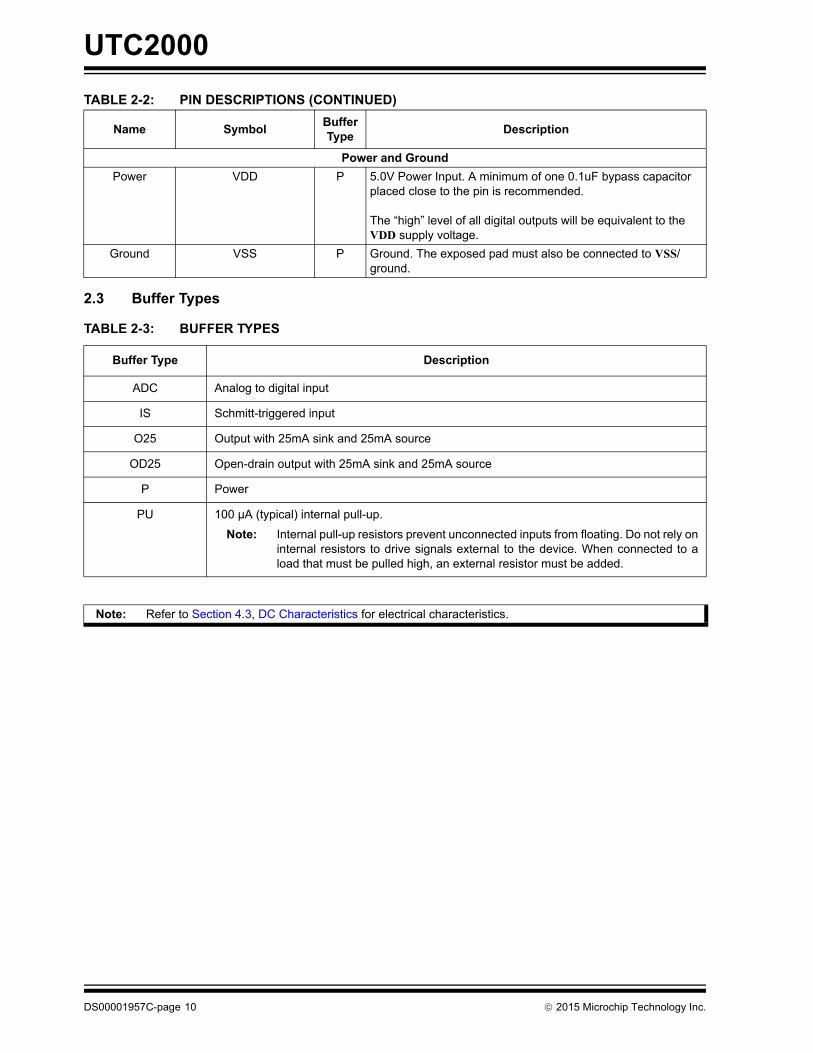
2.2 Pin Descriptions
TABLE 2-2: PIN DESCRIPTIONS
Name SymbolBuffer Type
Description
Digital Inputs
Controller Enable
ENABLE IS Active high enable signal. The UTC2000 will remain in its default, inactive state unless this pin is asserted high.
If unused, tie this pin to VDD through a 10kΩ pull-up resistor.
Fault Input OCS# IS(PU)
This active low signal is asserted by the +5V VBUS power sup-plying device to notify the UTC2000 when a system fault condi-tion has occurred. Typically, this signal is used for overcurrent or overvoltage conditions, but it can be used for any system related failure.
All digital control outputs will revert to their default, deasserted state when this pin is asserted. Normal operation will resume after deassertion of this pin.
After any OCS# assertion, a fault flag will be set and the FAULT_IND pin will assert. This flag is only cleared after a device reset or power cycle.
If unused, this pin can be left floating.
Analog Inputs
Configuration Selection
CFG_SEL ADC This analog to digital converter pin is sampled at power-on at Vcfg_samp to place the UTC2000 in either DFP or UFP mode.
Once in UFP mode, the UTC2000 will always remain in UFP mode and can only switch to DFP mode after a power-on reset.
Once in DFP mode, the UTC2000 can actively switch between 3.0A, 1.5A, or the default legacy (500mA USB 2.0, 900mA USB3.0/USB 3.1) DFP modes without power cycling. When switch-ing between DFP modes, the voltage thresholds and ranges for connection detection on the CC1/CC2 pins are modified accordingly.
Refer to Table 3-1 for additional details.
VBUS Voltage Monitor
VMON ADC This analog to digital converter pin monitors the input voltage on the VBUS pin of the USB receptacle.
The UTC2000 will enter the fault state and deassert all outputs if the voltage exceeds 0.8V on the VMON pin (>6.4V on VBUS).
A fault flag will be set and the FAULT_IND will assert after any overvoltage occurrence. This flag is only cleared after a device reset or power cycle.
This pin is required for UFP Modes. If unused in DFP Modes, tie this pin to GND through a 10kΩ pull-down resistor.
DS00001957C-page 8 2015 Microchip Technology Inc.

UTC2000
CC1 Monitor CC1 ADC This analog to digital converter input pin monitors the USB Type-CTM CC1 signal to detect various USB Type-C connec-tions.
Refer to Table 3-1for additional details.
CC2 Monitor CC2 ADC This analog to digital converter input pin monitors the USB Type-C CC2 signal to detect various USB Type-C connections.
See Table 3-1 for additional details.
Digital Outputs
+5V VBUS Power Supply
Enable
PPC_EN O25 DFP Modes Only. Active high output which controls the 5V supply to VBUS. This pin only asserts when a valid USB Type-C connection is detected.
PlugOrientationIndicator
PLUG_ORIENTATION# OD25 This active low output pin indicates the USB Type-C cable plug orientation.
This pin remains high in the default unconnected state or when an Rd pull-down resistor is detected on CC1.
The pin will assert low when an Rd pull-down resistor is detected on CC2.
CC1 VCONN Supply Control
VCONN1_OUT# OD25 DFP Modes Only. Open drain, active low VCONN supply con-trol to CC1 for supplying 5V to active cable circuitry. See Section 3.4 “VCONN Supply Control (DFP Modes Only)” for additional details.
CC2 VCONN Supply Control
VCONN2_OUT# OD25 DFP Modes Only. Open drain, active low VCONN supply con-trol to CC2 for supplying 5V to active cable circuitry. See Section 3.4 “VCONN Supply Control (DFP Modes Only)” for additional details.
Audio Adapter Indicator and
Control
AUDIO_ADAPTER O25 DFP Modes Only. Active high pin which indicates the detection of a USB audio adapter device. This pin is intended to control a high speed USB and audio switch which toggles between stan-dard USB 2.0 DP/DM Signaling and audio signaling.
Fault Indicator FAULT_IND O25 Active high fault indicator output. Output is asserted after an overcurrent event on OCS# is detected. Output is deasserted after toggling the ENABLE input pin or after a power-on reset.
Connected State Indicator
CONNECTED# OD25 UFP Mode Only. Open drain pin which asserts when a valid USB Type-C connection is detected on the CC pin, and when VBUS is within the valid voltage range.
Legacy Charging Indi-
cator
LEGACY_IND# OD25 UFP Mode Only. Open drain pin which asserts low when a valid USB Type-C connection is detected and Legacy 500mA/900mA charging capability is detected.
1.5A Charging Indicator
1.5A_IND# OD25 UFP Mode Only. Open drain pin which asserts low when a valid USB Type-C connection is detected and 1.5A USB Type-C charging capability is detected.
3.0A Charging Indicator
3.0A_IND# OD25 UFP Mode Only. Open drain pin which asserts low when a valid USB Type-C connection is detected and 3.0A USB Type-C charging capability is detected.
TABLE 2-2: PIN DESCRIPTIONS (CONTINUED)
Name SymbolBuffer Type
Description
2015 Microchip Technology Inc. DS00001957C-page 9
UTC2000
2.3 Buffer Types
Power and Ground
Power VDD P 5.0V Power Input. A minimum of one 0.1uF bypass capacitor placed close to the pin is recommended.
The “high” level of all digital outputs will be equivalent to the VDD supply voltage.
Ground VSS P Ground. The exposed pad must also be connected to VSS/ground.
TABLE 2-3: BUFFER TYPES
Buffer Type Description
ADC Analog to digital input
IS Schmitt-triggered input
O25 Output with 25mA sink and 25mA source
OD25 Open-drain output with 25mA sink and 25mA source
P Power
PU 100 µA (typical) internal pull-up.
Note: Internal pull-up resistors prevent unconnected inputs from floating. Do not rely oninternal resistors to drive signals external to the device. When connected to aload that must be pulled high, an external resistor must be added.
Note: Refer to Section 4.3, DC Characteristics for electrical characteristics.
TABLE 2-2: PIN DESCRIPTIONS (CONTINUED)
Name SymbolBuffer Type
Description
DS00001957C-page 10 2015 Microchip Technology Inc.

UTC2000
3.0 FUNCTIONAL DESCRIPTION
This chapter describes the functional descriptions for the following device sub-systems.
• Section 3.1, Configuration Selection
• Section 3.2, DFP Modes Functional State Machine
• Section 3.3, UFP Mode Functional State Machine
• Section 3.4, VCONN Supply Control (DFP Modes Only)
• Section 3.5, USB Audio Adapter (DFP Modes Only)
• Section 3.6, UFP Mode Connection and Charging Capability Detection Indicator
• Section 3.7, Connection and Disconnection Detection Debounce
3.1 Configuration Selection
The CFG_SEL pin is sampled at power-on at Vcfg_samp and the UTC2000 is placed in either UFP or DFP modes ofoperation.
If the CFG_SEL pin is within one of the DFP mode ranges upon power-on, it will operate in DFP mode. While in DFPmode, the CFG_SEL pin is constantly monitored and can be placed in any of the DFP modes at any time by the systemcontroller. Switching from DFP to UFP modes cannot be achieved without a power-on reset. Table 3-1 displays the volt-age ranges for the DFP profile.
If the CFG_SEL pin is within the UFP mode range upon power-on, it will operate in UFP mode. For UFP designs, it isrecommended to tie CFG_SEL to VDD through a pull-up resistor to ensure that UFP mode is entered when VDDcrosses the POR threshold. Switching from UFP to DFP modes cannot be achieved without a power-on reset. Table 3-2 displays the voltage ranges for the UFP profile.
TABLE 3-1: DFP CONFIGURATION SELECTION VOLTAGE MONITORING THRESHOLDS
CFG_SEL Voltage
ProfileCC1/CC2 No
Connection Voltage Range
CC1/CC2 Rd Detection Voltage
Range
CC1/CC2 Ra Detection Voltage
Range
1.2V - 1.3V 3A Capable DFP 5.0V - 2.75V 2.60V - 0.85V 0.80V - 0.00V
0.7V - 0.8V 1.5A Capable DFP 5.0V - 1.65V 1.60V - 0.45V 0.40V - 0.00V
0.0V - 0.30V Default Legacy USB Capable DFP
5.0V - 1.65V 1.60V - 0.25V 0.20V - 0.00V
TABLE 3-2: UFP CONFIGURATION SELECTION VOLTAGE MONITORING THRESHOLDS
CFG_SEL Voltage
No Connection Voltage Range
CC1/CC2 Legacy Charging Connection
Voltage Range
CC1/CC2 1.5A Charging Connection
Voltage Range
CC1/CC2 3.0A Charging Connection
Voltage Range
1.75V - VDD 0.0V - 0.25V 0.25V - 0.70V 0.70V-1.31V > 1.31V
2015 Microchip Technology Inc. DS00001957C-page 11

UTC2000
3.2 DFP Modes Functional State Machine
A visual representation of the UTC2000 DFP state machine behavior is shown in Figure 3-1. The various states aredetailed in the following sub-sections.
FIGURE 3-1: DFP MODES STATE MACHINE DIAGRAM
3.2.1 DISABLED IDLE
The UTC2000 will remain in a disabled, inactive state if ENABLE is asserted low, or the voltage on CFG_SEL is notwithin a valid configuration range.
While in this state, the state of the digital outputs are as follows:
• PPC_EN: Low
• PLUG_ORIENTATION#: High
• VCONN1_OUT#: High
• VCONN2_OUT#: High
• AUDIO_ADAPTER: Low
3.2.2 ENABLED IDLE
If both ENABLE is asserted high and CFG_SEL is in a valid configuration range, the UTC2000 will actively monitor theCC1 and CC2 pins for a connect event.
While in this state, the state of the digital outputs are as follows:
• PPC_EN: Low
• PLUG_ORIENTATION#: High
• VCONN1_OUT#: High
• VCONN2_OUT#: High
• AUDIO_ADAPTER: Low
DFP Mode CFG_SEL = 0.0V – 0.3V (Legacy Profile) or CFG_SEL = 0.7V – 0.8V (1.5A Profile) or CFG_SEL = 1.2V –1.3V (1.5A Profile)
Connection States
Enabled Idle(No Connection Detected)
PPC_EN = LowPLUG_ORIENTATION# = High
VCONN1_OUT# = HighVCONN2_OUT# =High
AUDIO ADAPTER = Low
Unflipped Passive Cable
PPC_EN = HighPLUG_ORIENTATION# = High
VCONN1_OUT# = HighVCONN2_OUT# = HighAUDIO ADAPTER = Low
Unflipped Powered Cable
PPC_EN = HighPLUG_ORIENTATION# = High
VCONN1_OUT# = HighVCONN2_OUT# = Low
AUDIO ADAPTER = Low
Flipped Passive Cable
PPC_EN = HighPLUG_ORIENTATION# = Low
VCONN1_OUT# = HighVCONN2_OUT# = HighAUDIO ADAPTER = Low
Flipped Powered Cable
PPC_EN = HighPLUG_ORIENTATION# = Low
VCONN1_OUT# = LowVCONN2_OUT# = HighAUDIO ADAPTER = Low
USB Audio Adapter
PPC_EN = LowPLUG_ORIENTATION# = High
VCONN1_OUT# = HighVCONN2_OUT# = HighAUDIO ADAPTER = High
CC1 detects RdCC2 detects NC
CC1 detects RdCC2 detects Ra
CC1 detects NCCC2 detects Rd
CC1 detects RaCC2 detects Rd
CC1 detects RaCC2 detects Ra
FaultDeassert all outputsSet FAULT_IND High
OCS# Asserted or
VMON > 0.8V(no debounce)
OCS# De-assertedand/or
VMON < 0.8V
ConnectionDetected
(100ms-200ms debounce)
ConnectionLost
(10-20ms debounce)
ENABLE Low > High
Disabled IdlePPC_EN = Low
PLUG_ORIENTATION# = HighVCONN1_OUT# = HighVCONN2_OUT# =High
AUDIO ADAPTER = LowENABLE
High > Low
changedetected, transition
to new state
10-20msdebounce
DS00001957C-page 12 2015 Microchip Technology Inc.

UTC2000
3.2.3 CONNECTED (UNFLIPPED PASSIVE CABLE)
If both ENABLE is asserted high and CFG_SEL is in a valid configuration range and an Rd pull-down resistor is sensedon the CC1 pin, the UTC2000 will enter the “CONNECTED (UNFLIPPED PASSIVE CABLE)” state.
While in this state, the state of the digital outputs are as follows:
• PPC_EN: High
• PLUG_ORIENTATION#: High
• VCONN1_OUT#: High
• VCONN2_OUT#: High
• AUDIO_ADAPTER: Low
3.2.4 CONNECTED (UNFLIPPED ACTIVE CABLE)
If ENABLE is asserted high, CFG_SEL is in a valid configuration range, an Rd pull-down resistor is sensed on the CC1pin, and an Ra pull-down resistor is sensed on the CC2 pin, the UTC2000 will enter the “CONNECTED (UNFLIPPEDACTIVE CABLE)” state.
While in this state, the state of the digital outputs are as follows:
• PPC_EN: High
• PLUG_ORIENTATION#: High
• VCONN1_OUT#: High
• VCONN2_OUT#: Low
• AUDIO_ADAPTER: Low
3.2.5 CONNECTED (FLIPPED PASSIVE CABLE)
If both ENABLE is asserted high and CFG_SEL is in a valid configuration range and an Rd pull-down resistor is sensedon the CC2 pin, the UTC2000 will enter the “CONNECTED (FLIPPED PASSIVE CABLE)” state.
While in this state, the state of the digital outputs are as follows:
• PPC_EN: High
• PLUG_ORIENTATION#: Low
• VCONN1_OUT#: High
• VCONN2_OUT#: High
• AUDIO_ADAPTER: Low
3.2.6 CONNECTED (FLIPPED ACTIVE CABLE)
If ENABLE is asserted high, CFG_SEL is in a valid configuration range, an Rd pull-down resistor is sensed on the CC2pin, and an Ra pull-down resistor is sensed on the CC1 pin, the UTC2000 will enter the “CONNECTED (UNFLIPPEDACTIVE CABLE)” state.
While in this state, the state of the digital outputs are as follows:
• PPC_EN: High
• PLUG_ORIENTATION#: Low
• VCONN1_OUT#: Low
• VCONN2_OUT#: High
• AUDIO_ADAPTER: Low
2015 Microchip Technology Inc. DS00001957C-page 13

UTC2000
3.2.7 CONNECTED (USB AUDIO ADAPTER)
If ENABLE is asserted high, CFG_SEL is in a valid configuration range, and Ra pull-down resistors are sensed on bothCC1 and CC2 pins the UTC2000 will enter the “CONNECTED (UNFLIPPED ACTIVE CABLE)” state.
While in this state, the state of the digital outs are as follows:
• PPC_EN: Low
• PLUG_ORIENTATION#: High
• VCONN1_OUT#: High
• VCONN2_OUT#: High
• AUDIO_ADAPTER: High
3.2.8 FAULT (OVERCURRENT OR OVERVOLTAGE)
If OCS# is asserted low while in any state, the UTC2000 will set all of its outputs to the default state and will transitioninto the fault state. An internal overcurrent flag will be set and FAULT_IND will drive high. Normal operation will resumeafter OCS# is deasserted. The FAULT_IND pin will continue to drive low until a power cycle occurs.
If VMON exceeds 0.8V at any state, the UTC2000 will set all of its outputs to the default state and will transition into thefault state. An internal overvoltage flag will be set and FAULT_IND will drive high. Normal operation will resume afterVMON is deasserted. The FAULT_IND pin will continue to drive low until a power cycle occurs.
Note: A typical USB audio adapter device will simply short CC1 and CC2 to ground. This implementation is func-tionally equivalent to using two Ra resistors.
DS00001957C-page 14 2015 Microchip Technology Inc.

UTC2000
3.3 UFP Mode Functional State Machine
A visual representation of the UTC2000 UFP state machine behavior is shown in Figure 3-2. The various states aredetailed in the following sub-sections.
FIGURE 3-2: UFP MODE STATE MACHINE DIAGRAM
3.3.1 IDLE
The UTC2000 will remain in a disabled, inactive state if ENABLE is asserted low, or the voltage on CFG_SEL is notwithin a valid configuration range.
While in this state, the state of the digital outputs are as follows:
• CONNECTED#: High (Not Asserted)
• PLUG_ORIENTATION#: High (Not Asserted)
• LEGACY_IND#: High (Not Asserted)
• 1.5A_IND#: High (Not Asserted)
• 3.0A_IND#: High (Not Asserted)
UFP Mode CFG_SEL = 1.75V – VDD
Idle(No Connection Detected)
CONNECTED# = HighPLUG_ORIENTATION# = High
LEGACY_IND# = High1.5A_IND# = High3.0A_IND# = High
FaultDeassert all outputsSet FAULT_IND High
OCS# Asserted or
VMON > 0.8V(no debounce)
OCS# De-assertedand/or
VMON < 0.8V
Connection States0.5 < VMON < 0.6875V(4.0 < VBUS < 5.5V)
Unflipped Legacy Connection
CONNECTED# = LowPLUG_ORIENTATION# = High
LEGACY_IND# = Low1.5A_IND# = High3.0A_IND# = High
Unflipped 1.5A Connection
CONNECTED# = LowPLUG_ORIENTATION# = High
LEGACY_IND# = High1.5A_IND# = Low3.0A_IND# = High
Unflipped 3.0A Connection
CONNECTED# = LowPLUG_ORIENTATION# = High
LEGACY_IND# = High1.5A_IND# = High3.0A_IND# = Low
Flipped Legacy Connection
CONNECTED# = LowPLUG_ORIENTATION# = Low
LEGACY_IND# = Low1.5A_IND# = High3.0A_IND# = High
Fllipped 1.5A Connection
CONNECTED# = LowPLUG_ORIENTATION# = Low
LEGACY_IND# = High1.5A_IND# = Low3.0A_IND# = High
CC1 detects LegacyCC2 detects NC
CC1 detects 1.5ACC2 detects NC
CC1 detects 3.0ACC2 detects NC
CC1 detects NCCC2 detects Legacy
CC1 detects NCCC2 detects 1.5A
Fllipped 3.0A Connection
CONNECTED# = LowPLUG_ORIENTATION# = Low
LEGACY_IND# = High1.5A_IND# = High3.0A_IND# = Low
CC1 detects NCCC2 detects 3.0A
ConnectionDetected
(100-150ms debounce)
ConnectionLost
(10-20ms debouce)
changedetected, transition
to new state
10-20msdebounce
2015 Microchip Technology Inc. DS00001957C-page 15

UTC2000
3.3.2 CONNECTED (UNFLIPPED LEGACY CONNECTION)
If VBUS is in a valid range (4.5V-5.5V) and a Legacy Rp pull-up resistor is sensed on the CC1 pin (and no connectiondetected on the CC2 pin) the UTC2000 will enter the “CONNECTED (UNFLIPPED LEGACY CONNECTION)” state.
While in this state, the state of the digital outputs are as follows:
• CONNECTED#: Low (Asserted)
• PLUG_ORIENTATION#: High (Not Asserted)
• LEGACY_IND#: Low (Asserted)
• 1.5A_IND#: High (Not Asserted)
• 3.0A_IND#: High (Not Asserted)
3.3.3 CONNECTED (UNFLIPPED 1.5A CONNECTION)
If VBUS is in a valid range (4.5V-5.5V) and a 1.5A Rp pull-up resistor is sensed on the CC1 pin (and no connectiondetected on the CC2 pin) the UTC2000 will enter the “CONNECTED (UNFLIPPED 1.5A CONNECTION)” state.
While in this state, the state of the digital outputs are as follows:
• CONNECTED#: Low (Asserted)
• PLUG_ORIENTATION#: High (Not Asserted)
• LEGACY_IND#: High (Not Asserted)
• 1.5A_IND#: Low (Asserted)
• 3.0A_IND#: High (Not Asserted)
3.3.4 CONNECTED (UNFLIPPED 3.0A CONNECTION)
If VBUS is in a valid range (4.5V-5.5V) and a 3.0A Rp pull-up resistor is sensed on the CC1 pin (and no connectiondetected on the CC2 pin) the UTC2000 will enter the “CONNECTED (UNFLIPPED 3.0A CONNECTION)” state.
While in this state, the state of the digital outputs are as follows:
• CONNECTED#: Low (Asserted)
• PLUG_ORIENTATION#: High (Not Asserted)
• LEGACY_IND#: High (Not Asserted)
• 1.5A_IND#: High (Not Asserted)
• 3.0A_IND#: Low (Asserted)
3.3.5 CONNECTED (FLIPPED LEGACY CONNECTION)
If VBUS is in a valid range (4.5V-5.5V) and a Legacy Rp pull-up resistor is sensed on the CC2 pin (and no connectiondetected on the CC1 pin) the UTC2000 will enter the “CONNECTED (FLIPPED LEGACY CONNECTION)” state.
While in this state, the state of the digital outputs are as follows:
• CONNECTED#: Low (Asserted)
• PLUG_ORIENTATION#: Low (Asserted)
• LEGACY_IND#: High (Asserted)
• 1.5A_IND#: High (Not Asserted)
• 3.0A_IND#: High (Not Asserted)
DS00001957C-page 16 2015 Microchip Technology Inc.

UTC2000
3.3.6 CONNECTED (FLIPPED L1.5A CONNECTION)
If VBUS is in a valid range (4.5V-5.5V) and a 1.5A Rp pull-up resistor is sensed on the CC2 pin (and no connectiondetected on the CC1 pin) the UTC2000 will enter the “CONNECTED (FLIPPED 1.5A CONNECTION)” state.
While in this state, the state of the digital outputs are as follows:
• CONNECTED#: Low (Asserted)
• PLUG_ORIENTATION#: Low (Asserted)
• LEGACY_IND#: High (Not Asserted)
• 1.5A_IND#: Low (Asserted)
• 3.0A_IND#: High (Not Asserted)
3.3.7 CONNECTED (FLIPPED 3.0A CONNECTION)
If VBUS is in a valid range (4.5V-5.5V) and a 3.0A Rp pull-up resistor is sensed on the CC2 pin (and no connectiondetected on the CC1 pin) the UTC2000 will enter the “CONNECTED (FLIPPED 3.0A CONNECTION)” state.
While in this state, the state of the digital outputs are as follows:
• CONNECTED#: Low (Asserted)
• PLUG_ORIENTATION#: Low (Asserted)
• LEGACY_IND#: High (Not Asserted)
• 1.5A_IND#: High (Not Asserted)
• 3.0A_IND#: Low (Asserted)
3.3.8 FAULT (OVERCURRENT OR OVERVOLTAGE)
If OCS# is asserted low while in any state, the UTC2000 will set all of its outputs to the default state and will transitioninto the fault state. An internal overcurrent flag will be set and FAULT_IND will drive high. Normal operation will resumeafter OCS# is deasserted. The FAULT_IND pin will continue to drive low until a reset or power cycle occurs.
If VMON exceeds 0.8V (6.4V on VBUS) at any state, the UTC2000 will set all of its outputs to the default state and willtransition into the fault state. An internal overvoltage flag will be set and FAULT_IND will drive high. Normal operationwill resume after VMON is deasserted. The FAULT_IND pin will continue to drive low until a reset or power cycle occurs.
3.4 VCONN Supply Control (DFP Modes Only)
VCONN1_OUT# and VCONN2_OUT# are open drain, active low output signals used to control a 5V voltage supply topower a powered USB Type-C cable. Powered cable support is mandatory for all USB Type-C applications which imple-ment USB 3.0/USB 3.1. For USB 2.0 systems, powered cable support is optional. The VCONN supply control signalswill assert low when one of the following conditions are met:
• VCONN1_OUT# will assert low if an Rd resistor is detected on CC2 and an Ra resistor is detected on CC1. The signal will remain asserted until the Rd resistor on CC2 is no longer sensed (USB cable is detached).
• VCONN2_OUT# will assert low if an Rd resistor is detected on CC1 and an Ra resistor is detected on CC2. The signal will remain to asserted until the Rd resistor on CC1 is no longer sensed (USB cable is detached).
3.5 USB Audio Adapter (DFP Modes Only)
AUDIO_ADAPTER is an active high output signal that is used to indicate when a USB audio adapter is detected.AUDIO_ADAPTER will assert high when an Ra resistor is detected on both CC1 and CC2 pins. The signal will remainasserted until either or both Ra resistors is no longer sensed. This signal is intended to control a high-speed switch thattoggles between USB differential data and an audio signal.The switch that is selected must be capable of supportingUSB 2.0 as well as audio signals ranging from -3.0V to +3.0V. Additional electrical details can be found in section A-3of the USB Type-CTM Cable and Connector Specification.
Note: Additional details for implementing Audio Adapter mode are detailed in Appendix A of the USB Type-CTM
Cable and Connector Specification.
2015 Microchip Technology Inc. DS00001957C-page 17

UTC2000
Two additional signals are also used when operating in Audio Adapter mode. These signals are Mic/AGND and AGND/Mic which should be connected to SBU1 and SBU2 respectively.
3.6 UFP Mode Connection and Charging Capability Detection Indicator
While operating in UFP mode, there are 4 outputs that indicate connection state.
CONNECTED# is an open drain output that asserts when any of the three valid USB Type-C connections are detected.Legacy charging mode (500mA for USB 2.0 connections, 900mA for USB 3.0/USB 3.1 connections) is detected whena DFP with a 56k Rp pull-up resistor is detected. 1.5A charging is detected when a DFP with a 22k Rp pull-up resistoris detected. 3.0A charging is detected when a DFP with a 10k Rp pull-up resistor is detected.
The LEGACY_IND#, 1.5A_IND#, and 3.0A_IND# open drain outputs assert low to indicate which type of connectionwas detected. These outputs can be fed to the battery charging management circuitry of the USB device to appropriatelyregulate the amount of current draw.
The CONNECTED# signal may also be used to gate the VBUS voltage to system power if an added level of protectionfrom high voltage is desired.
3.7 Connection and Disconnection Detection Debounce
A debounce is implemented to eliminate unwanted connect/disconnect events due to cable jostling or USB Power Deliv-ery messaging.
A transition from the ENABLED IDLE state to any connected state is debounced by 100ms-200ms.
A transition from any connected state to any other connected state or from any connected state to the ENABLED IDLEstate is debounced by 10ms-20ms.
DS00001957C-page 18 2015 Microchip Technology Inc.

UTC2000
4.0 OPERATIONAL CHARACTERISTICS
4.1 Absolute Maximum Ratings(†)
Ambient temperature under bias............................................................................................................ -40°C to +125°C
Storage temperature .............................................................................................................................. -65°C to +150°C
Voltage on pins with respect to VSS
on VDD pin .................................................................................................................................. -0.3V to +6.5V
on all other pins .............................................................................................................. -0.3V to (VDD + 0.3V)
Maximum current
on VSS pin(4-1)
0°C ≤ TA ≤ +70°C ..................................................................................................................... 95 mA
-40°C ≤ TA ≤ +85°C .................................................................................................................. 85 mA
-40°C ≤ TA ≤ +125°C ................................................................................................................ 35 mA
on VDD pin(1)
0°C ≤ TA ≤ +70°C ..................................................................................................................... 95 mA
-40°C ≤ TA ≤ +85°C .................................................................................................................. 85 mA
-40°C ≤ TA ≤ +125°C ................................................................................................................ 35 mA
on any I/O pin ....................................................................................................................................... ±25 mA
Clamp current, IK (VPIN < 0 or VPIN > VDD) ......................................................................................................... ±20 mA
Note 4-1 Maximum current rating requires even load distribution across I/O pins. Maximum current rating maybe limited by the device package power dissipation characterizations.
4.2 Standard Operating Conditions
The standard operating conditions for this device are defined as:
Operating Voltage: VDDMIN ≤ VDD ≤ VDDMAX
Operating Temperature: TA_MIN ≤ TA ≤ TA_MAX
VDD — Operating Supply Voltage(4-2)
VDDMIN ....................................................................................................................................... +4.5V
VDDMAX ...................................................................................................................................... +5.5V
TA — Operating Ambient Temperature Range
Commercial Temperature
TA_MIN ........................................................................................................................................... 0°C
TA_MAX ...................................................................................................................................... +70°C
Industrial Temperature
TA_MIN ........................................................................................................................................ -40°C
TA_MAX ...................................................................................................................................... +85°C
Extended Temperature
TA_MIN ........................................................................................................................................ -40°C
TA_MAX .................................................................................................................................... +125°C
Note 4-2 Refer to Parameter D001, DC Characteristics: Supply Voltage.
† NOTICE: Stresses above those listed under “Absolute Maximum Ratings” may cause permanent damage to thedevice. This is a stress rating only and functional operation of the device at those or any other conditions above thoseindicated in the operation listings of this specification is not implied. Exposure above maximum rating conditions forextended periods may affect device reliability.
2015 Microchip Technology Inc. DS00001957C-page 19

UTC2000
4.3 DC Characteristics
FIGURE 4-1: POR AND POR REARM WITH SLOW RISING VDD
TABLE 4-1: SUPPLY VOLTAGEParam.
No.Sym. Characteristic Min. Typ† Max. Units Conditions
D001 VDD Supply Voltage
Vddmin4.5 —
Vddmax5.5 V
D002* VPOR Power-on Reset Release Voltage(1)
— 1.6 — V
D003 VPORR* Power-on Reset Rearm Voltage(1)
— 0.8 — V
D004 SVDD VDD Rise Rate(2) 0.05 — — V/ms Ensures that the Power-on Reset signal is released
properly.
D005 VCFG_SAMP CFG_SEL Sampling Threshold Voltage
— 3.6 — V
* These parameters are characterized but not tested.
Note 1: See Figure 4-1, POR and POR REARM with Slow Rising VDD.
VDD
VPOR
VPORR
VSS
VSS
NPOR(1)
TPOR(2)
POR REARM
Note 1: When NPOR is low, the device is held in Reset.
2: TPOR 1 μs typical.
3: TVLOW 2.7 μs typical.
TVLOW(3)
SVDD
DS00001957C-page 20 2015 Microchip Technology Inc.

UTC2000
TABLE 4-2: SUPPLY CURRENT (IDD)(1)
Param.No.
Device Characteristics
Min. Typ Max. UnitsConditions
VDD Note
D006 Disabled — 185 205 uA 5.0 -40°C ≤ TA ≤ +85°C
D007 Enabled — 185 205 uA 5.0 -40°C ≤ TA ≤ +85°C
D008 Enabled & Connected — 1.30 1.35 mA 5.0 -40°C ≤ TA ≤ +85°C
Note 1: The supply current is mainly a function of the operating voltage. Other factors, such as I/O pin loading and switching rate also have an impact on the current consumption.
TABLE 4-3: I/O PORTSStandard Operating Conditions (unless otherwise stated)
Param.No.
Sym. Characteristic Min. Typ† Max. Units Conditions
VIL Input Low Voltage
I/O PORT:
D009 — — 0.8 V 4.5V ≤ VDD ≤ 5.5V
D009A — — 0.15 VDD V 3.0V ≤ VDD ≤ 4.5V
VIH Input High Voltage
D010 2.0 — — V 4.5V ≤ VDD ≤ 5.5V
D010A 0.25 VDD + 0.8
— — V 3.0V ≤ VDD ≤ 4.5V
IIL Input Leakage Current(1)
D011 I/O Ports — ± 5 ± 125 nA VSS ≤ VPIN ≤ VDD, Pin at high-impedance, 85°C
— ± 5 ± 1000 nA VSS ≤ VPIN ≤ VDD, Pin at high-impedance, 125°C
VOL Output Low Voltage
D012 I/O Ports—
— 0.6 V Iol = 8 mA, Vdd = 5VIol = 6 mA, Vdd = 3.3V
Iol = 1.8 mA, Vdd = 1.8V
Voh Output High Voltage
D013 I/O Ports Vdd - 0.7 — — V Ioh = 3.5 mA, Vdd = 5VIoh = 3 mA, Vdd = 3.3VIoh = 1 mA, Vdd = 1.8V
Capacitive Loading Specifications on Output Pins
D014* CIO All I/O pins — — 50 pF
* These parameters are characterized but not tested.† Data in “Typ” column is at 5.0V, 25°C unless otherwise stated. These parameters are for design guidance only and are
not tested.Note 1: Negative current is defined as current sourced by the pin.
2015 Microchip Technology Inc. DS00001957C-page 21

UTC2000
TABLE 4-5: THERMAL CHARACTERISTICS
TABLE 4-4: TIMING PARAMETERSStandard Operating Conditions (unless otherwise stated)
Param. No. Sym. Min. Typ† Max. Units
tCONNECT_DEBOUNCE CC1/CC2 Connection Detection Debounce Delay
D015 100 160 200 ms
tDISCONNECT_DEBOUNCE CC1/CC2 Disconnection or Connection Change Debounce Delay
D016 10 16 20 ms
tVMON_FAULT VMON Fault Detection Reaction Delay
D017 — 0.460 1 ms
tOCS#_FAULT OCS# Fault Detection Reaction Delay
D018 — 0.410 1 ms
† Data in “Typ” column is at 3.0V, 25°C unless otherwise stated.
Standard Operating Conditions (unless otherwise stated)
Param.No.
Sym. Characteristic Typ. Units Conditions
TH01 θJA Thermal Resistance Junction to Ambient
55.3 °C/W 16-pin QFN 3x3x0.9mm package
TH02 θJC Thermal Resistance Junction to Case
10 °C/W 16-pin QFN 3x3x0.9mm package
TH03 TJMAX Maximum Junction Temperature 150 °CTH04 PD Power Dissipation — W PD = PINTERNAL + PI/O
TH05 Pinternal Internal Power Dissipation — W PINTERNAL = IDD x VDD(1)
TH06 PI/O I/O Power Dissipation — W PI/O = Σ (IOL * VOL) + Σ (IOH * (VDD - VOH))
TH07 PDER Derated Power — W PDER = PDMAX (TJ - TA)/θJA(2)
Note 1: IDD is current to run the chip alone without driving any load on the output pins.
2: TA = Ambient Temperature; TJ = Junction Temperature
DS00001957C-page 22 2015 Microchip Technology Inc.

UTC2000
5.0 UTC2000 SYSTEM APPLICATION
This chapter explains external requirements for UTC2000 applications and provides some example diagrams.
• Section 5.1, 5V VBUS Switch (DFP Modes Only)
• Section 5.2, Rp Pull-Up Resistor (DFP Modes Only)
• Section 5.3, Rd Pull-Down Resistor (UFP Mode Only)
• Section 5.4, VCONN Active Cable Supply (DFP Modes Only)
• Section 5.5, CC Pin Isolation (DFP Only)
• Section 5.6, CC Pin Current Limiting Resistors (UFP Only)
• Section 5.7, VBUS Monitoring
• Section 5.8, USB Signal Multiplexer
• Section 5.9, Application Example: 3.0A Capable USB 3.0/USB 3.1 DFP
• Section 5.10, Application Example: 1.5A Capable USB 2.0 DFP
• Section 5.11, Application Example: 500mA Capable USB 2.0 DFP with Audio Adapter Support
• Section 5.12, Application Example: 3.0A Capable USB Type-CTM Charging Port (AC Adapter)
• Section 5.13, Application Example: UFP Device
5.1 5V VBUS Switch (DFP Modes Only)
A 5V USB port power switch with active high enable input and an overcurrent indicator output is required. The USBType-C receptacle must not supply 5V to the VBUS pins until a valid connection is detected. The UTC2000 controllerasserts the active high PPC_EN signal to control the 5V port power supply to VBUS upon detection of a valid USB Type-C connection. The port power switch controlled by the UTC2000 shall also have built in overcurrent detection set to athreshold that is appropriate for the current capability profile that is being selected per Table 5-1. An overcurrent thresh-old of 125% (of the selected DFP profile current) is appropriate, as the threshold may not be tripped at any current lessthan or equal to the selected current profile. The 5V VBUS port power controller should indicate that an overcurrentevent has occurred by pulling the OCS# signal to the UTC2000 controller low.
5.2 Rp Pull-Up Resistor (DFP Modes Only)
A Downstream Facing Port is required to supply voltage to both CC pins through a pull-up resistor. The pull-up voltagemay be either 5.0V volts or 3.3V. A UFP must implement a Rd pull-down resistor to ground. When a DFP to UFP con-nection is made, a resistor divider is formed, and the voltage at the CC pin can be measured to interpret the type ofconnection. Table 5-1 describes the possible values of the Rp pull-up resistor.
The UTC2000 measures the voltages on both CC pins via it’s internal ADCs. The CC pin voltage ranges, as defined inthe USB Type-CTM Cable and Connector Specification, are shown in Table 3-1.
5.3 Rd Pull-Down Resistor (UFP Mode Only)
An Upstream Facing Port is required to implement a 5.1k +/- 10% Rd pull-down resistor to ground connected to bothCC1 and CC2 pins on the Type-C receptacle. When a DFP to UFP connection is made, a resistor divider is formed, andthe voltage at the CC pin can be measured to interpret the charging capability of the DFP.
Note: A constant current source may also be implemented instead of a pull-up resistor.
TABLE 5-1: RP PULL-UP RESISTOR VALUES
DFP AdvertisementResistor Pull-Up
to 4.75 - 5.5VResistor Pull-Up
to 3.3V ± 5%Current Source
Legacy USB:500mA USB 2.0
900mA USB 3.0/USB 3.1
56 kΩ ± 20% 36 kΩ ± 20% 80 µA ± 20%
1.5A 22 kΩ ± 5% 12 kΩ ± 5% 180 µA ± 8%
3.0A 10 kΩ ± 5% 4.7 kΩ ± 5% 330 µA ± 8%
2015 Microchip Technology Inc. DS00001957C-page 23

UTC2000
5.4 VCONN Active Cable Supply (DFP Modes Only)
All USB Type-C receptacles must be able to supply power to an active cable if USB 3.0/USB 3.1 signaling is imple-mented. Supplying VCONN is optional if only USB 2.0 is implemented. The simplest implementation is to add a FET (orseries of FETs) that switches in the VCONN voltage directly to the CC pin node. The VCONN supply must be capableof supplying 1.0W of continuous power and may not supply more than 1.25A at the moment of plug contact. A bulkcapacitance of 10µF to 220µF must also be switched in with VCONN. The bulk capacitance may not need to be a dis-crete capacitor if the supply’s output capacitance already meets this requirement. Overcurrent detection is recom-mended, but not required per the USB Type-CTM Cable and Connector Specification. A simple implementation exampleis shown in Figure 5-1 below.
FIGURE 5-1: EXAMPLE VCONN SUPPLY CONNECTION
5.5 CC Pin Isolation (DFP Only)
The CC pins on a DFP must be high-impedance when the DFP is powered off. This is to prevent VBUS backdrive in asituation when a DFP connects to an unpowered DFP and detects the Rp pull-up resistors as an Rd pull-down. There-fore, it is recommended that some isolation FETs are implemented that disconnect the CC pins from the Rp pull-up resis-tors and VCONN supply circuitry when powered off.
5.6 CC Pin Current Limiting Resistors (UFP Only)
Because most UFP designs require operation even when unpowered, resistors placed directly in front of the CC1 andCC2 pins are recommended to limit the amount of leakage current through the UTC2000 ADC inputs when unpowered.10kΩ resistors are the recommended value.
Failure to place current limiting resistors could result in a failure to detect a USB attach due to a shift in CC voltage.
Note: Rds_on must be carefully considered to ensure that the USB Type-CTM Cable and Connector Specificationrequirements for VCONN supply current and voltage range are met.
Note: It is also recommended to implement additional circuitry to make the CC1 and CC2 pins high impedancewhen the DFP is in an unpowered state. Refer to Figure 5-7 for an example.
VCONN1_OUT#
VCONN2_OUT#
Rp Pull-Up Voltage
CC1
CC2
Rp Rp
10uF-220uFBulk Cap
VCONN 1.0W Supply
DS00001957C-page 24 2015 Microchip Technology Inc.

UTC2000
5.7 VBUS Monitoring
DFP Modes: An optional VBUS monitoring function may be implemented to protect the system from higher thanexpected voltages on VBUS (from a malfunctioning connected USB device) by preventing the UTC2000 from enablingthe 5V port switch. Additional back-drive protection or isolation circuitry must be implemented for thorough protection.This feature requires the VMON pin to be connected to VBUS through a resistor divider network that divides the VBUSvoltage by a factor of 8. A 35.7kΩ resistor over a 5.1kΩ resistor is recommended, as shown in the Figure 5-7, Figure 5-8, and Figure 5-9 below.
UFP Mode: The VBUS monitoring function is required and used to verify a valid VBUS range before asserting the CON-NECTED pin or any charge capability indicator outputs. A fault condition will also be flagged if higher than expectedvoltage on VBUS (from a malfunctioning connected USB device) is detected. Additional back-drive protection or isola-tion circuitry must be implemented for thorough protection. This features requires the VMON pin to be connected toVBUS through a resistor divider network that divides the VBUS voltage by a factor of 8.
5.8 USB Signal Multiplexer
There are several options for connecting the USB signals to the USB Type-C receptacles. These options differ slightlybetween USB 2.0 and USB 3.0/USB 3.1 applications, as detailed in the following sub-sections.
5.8.1 USB 2.0 OPTION 1: HIGH-SPEED MULTIPLEXER/SWITCH
The most robust solution for USB 2.0 applications is to use a USB High-Speed switch to control the routing of the USBsignals. The Microchip USB3740 is a cost-effective solution for this purpose and offers several benefits:
• Extreme ESD: +- 15KV (IEC)
• Low Power: 5uA(on), 1uA (off)
• Off Isolation: less than -40dB
• High bandwidth: up to 1 GHz
• Preserves signal integrity
• Small Package: 1.3 x 1.8 mm – 10pin DFN (.4mm pitch)
FIGURE 5-2: BLOCK DIAGRAM OF USB 2.0 OPTION 1: HIGH-SPEED SWITCH
MicrochipUSB3740
Switch
USB2.0Host/Hub/
Device
USB Type-C
TM Connector
DP
DM
DP
DM
DP1
DM1
DP2
DP2S
PLUG_ORIENTATION#(from UTC2000)
A6A7
B6B7
D+
D-
D+
D-
DP
DMDP
DM
2015 Microchip Technology Inc. DS00001957C-page 25

UTC2000
5.8.2 USB 2.0 OPTION 2: SHORT DP/DM PINS TOGETHER
The simplest solution is to short together the DP / DM pins at the receptacle. Only one DP / DM pair at the connectorwill be active at once. Note that this implementation will negatively affect the integrity of the USB signals because of thecreation of stubs on the USB traces.
FIGURE 5-3: BLOCK DIAGRAM OF USB 2.0 OPTION 2: SHORT DP/DM PINS TOGETHER
5.8.3 USB 2.0 OPTION 3: USE TWO DOWNSTREAM PORTS (DFP ONLY)
If two downstream ports are available, then they may both be connected to the DP / DM pins on the USB Type-C recep-tacle. Only one of the ports will be active and able to be used at once.
FIGURE 5-4: BLOCK DIAGRAM OF USB 2.0 OPTION 3: USE TWO DOWNSTREAM PORTS
Note: If using a Microchip Hub with FlexConnect, a muxless UFP design is possible. Refer to the MicrochipUSB5734 USB Type-C Reference Design and Evaluation Platform for details.
USB2.0Host/Hub/
Device
DPDP
DM
A6
A7
B6
B7
D+
D-
D+
D-
DM
USB Host/Hub
USB Type-C
TM Connector
DP1
DM1
DP2
DP2
A6A7
B6B7
D+
D-
D+
D-
DP
DM
DS00001957C-page 26 2015 Microchip Technology Inc.

UTC2000
5.8.4 USB 3.0/USB 3.1 OPTION 1: SUPER SPEED MULTIPLEXER/SWITCH
In a USB 3.0/USB 3.1 UFP application, or a USB 3.0/USB 3.1 DFP application where only one downstream port is avail-able, a Super-Speed USB 3.0/USB 3.1 switch must be used to control the routing of the USB signals.
FIGURE 5-5: BLOCK DIAGRAM OF USB 3.0/USB 3.1 OPTION 1: SUPER-SPEED MUX/SWITCH
USB3.0/USB 3.1
Super-SpeedMux
USB 3.0/USB 3.1Host/Hub/
Device
USB Type-C
TM Connector
DP
DM
DP
DM
S
PLUG_ORIENTATION#(from UTC2000)
A6A7
B6B7
D+
D-
D+
D-
SSRX+
SSRX-
SSRX+
SSRX-
SSTX+
SSTX-
SSTX+
SSTX-
DP
DM
SSRX1+
SSRX1-
SSTX1+
SSTX1-
DP
DM
SSRX2+
SSRX2-
SSTX2+
SSTX2-
B11B10 RX1-
RX1+
A2A3 TX1-
TX1+
B11B10 RX1-
RX1+
A2A3 TX1-
TX1+
2015 Microchip Technology Inc. DS00001957C-page 27

UTC2000
5.8.5 USB 3.0/USB 3.1 OPTION 2: USE TWO DOWNSTREAM PORTS (DFP ONLY)
If two downstream ports are available, then they may both be connected to the USB pins on the USB Type-C receptacle.Only one of the ports will be active and able to be used at once.
FIGURE 5-6: BLOCK DIAGRAM OF USB 3.0/USB 3.1 OPTION 2: USE TWO DOWNSTREAM PORTS
Note: If using a Microchip Hub with FlexConnect, a muxless UFP design is possible. Refer to the MicrochipUSB5734 Type-C Reference Design and Evaluation Platform for details.
USB 3.0/USB 3.1Host/Hub
USB Type-C
TM Connector
DP
A6A7
B6B7
D+
D-
D+
D-
DP1
DM1
SSRX1+
SSRX1-
SSTX1+
SSTX1-
DP2
DM2
SSRX2+
SSRX2-
SSTX2+
SSTX2-
B11B10 RX1-
RX1+
A2A3 TX1-
TX1+
B11B10 RX1-
RX1+
A2A3 TX1-
TX1+
DS00001957C-page 28 2015 Microchip Technology Inc.

UTC2000
5.9 Application Example: 3.0A Capable USB 3.0/USB 3.1 DFP
FIGURE 5-7: USB 3.0/USB 3.1 APPLICATION SCHEMATIC
TM
2015 Microchip Technology Inc. DS00001957C-page 29

UTC2000
5.10 Application Example: 1.5A Capable USB 2.0 DFP
FIGURE 5-8: USB 2.0 APPLICATION SCHEMATIC
5.11 Application Example: 500mA Capable USB 2.0 DFP with Audio Adapter Support
FIGURE 5-9: USB 2.0 WITH AUDIO ADAPTER APPLICATION SCHEMATIC
TM
TM
DS00001957C-page 30 2015 Microchip Technology Inc.

UTC2000
5.12 Application Example: 3.0A Capable USB Type-CTM Charging Port (AC Adapter)
FIGURE 5-10: 3.0A CHARGING PORT (AC ADAPTER) APPLICATION SCHEMATIC
5.13 Application Example: UFP Device
FIGURE 5-11: UFP DEVICE APPLICATION SCHEMATIC
TM
0.1uF
5V
R_SENSE
GND
TX1+ A2
TX1- A3
CC1 A5
D+ A6
D- A7
SBU1 A8
RX2- A10
RX2+ A11
TX2+ B2
TX2- B3
CC2 B5
D+ B6
D- B7
SBU2 B8
VBUS
RX1- B10RX1+ B11
USB Type C
5V
10k
To PWR Management
5.1lk 5.1k
TX-
RX+
S
TX-A
RX-
TX+A
RX-ARX+A
TX+BTX-B
RX-BRX+B
TX+
USB3.0 Switch
USB2 DPUSB2 DM
USB3 RX-USB3 RX+
USB3 TX-USB3 TX+
CC17
VDD 16
VSS 13
EPAD
VMON12
CC26
1.5A_IND#9
LEGACY_IND#8
OCS#1
ENABLE 3CONNECTED#5
PLUG_ORIENTATION#11
FAULT_IND 4
CFG_SEL 2
3.0A_IND#10
UTC2000
+ -
OCS
Current Sense
To PWR ManagementTo PWR Management
To PWR Management
35.7k
5.1k
To System Power
5V
10k
10k10k 10k
2015 Microchip Technology Inc. DS00001957C-page 31

UTC2000
Note: The pass FET and current sense circuitry connected to VBUS are for high voltage protection and areoptional. If high voltage protection is required and the device is bus powered or battery powered (and mayhave a dead battery), a high voltage tolerant regulator must also be implemented to power the UTC2000while it qualifies the USB Type-C connection.
DS00001957C-page 32 2015 Microchip Technology Inc.

UTC2000
6.0 PACKAGING INFORMATION
6.1 Package Marking Information
FIGURE 6-1: 16-PIN QFN PACKAGE MARKING INFORMATION
Note: For the most current package drawings, please see the Microchip Packaging Specification located at http://www.microchip.com/packaging
Legend: UC UTC2000 DesignatorX Temperature range designator:
(Blank=commercial, i=industrial, e= extended)A Automotive designator
(0=non-automotive, V=automotive)YY Year code (last two digits of calendar year)WW Week code (week of January 1 is week ‘01’)NNN Alphanumeric traceability code
Note: In the event the full Microchip part number cannot be marked on one line, itwill be carried over to the next line, thus limiting the number of availablecharacters for customer-specific information.
Example
PIN 1 PIN 1
16-Lead QFN (3x3x0.9 mm)
2015 Microchip Technology Inc. DS00001957C-page 33

UTC2000
6.2 Package Details
FIGURE 6-2: 16-PIN QFN PACKAGE (DRAWING)
DS00001957C-page 34 2015 Microchip Technology Inc.

UTC2000
FIGURE 6-3: 16-PIN QFN PACKAGE (DIMENSIONS)
2015 Microchip Technology Inc. DS00001957C-page 35

UTC2000
FIGURE 6-4: 16-PIN QFN PACKAGE (LAND PATTERN)
DS00001957C-page 36 2015 Microchip Technology Inc.

UTC2000
APPENDIX A: DATA SHEET REVISION HISTORY
TABLE A-1: REVISION HISTORY
Revision Level & Date Section/Figure/Entry Correction
DS00001957C (08-06-15) Cover, Section 1.1, "General Description", Section 4.2,
"Standard Operating Condi-tions", Figure 6-1, Product Identification System on
page 40
• Changed “Automotive extended temperature” to “extended temperature” as the extended temperature range is available in automotive and non-automotive versions.
• Updated “XXX” automotive code description.
Table 2.2, "Pin Descriptions" Updated first sentence of CFG_SEL description
Section 3.1, "Configuration Selection"
• Updated first sentence to reference VCFG_SAMP
• Updated 2nd and 3rd paragraph to make the mode ranges conditional “upon power-on”.
• Added new sentence to third paragraph: “For UFP designs, it is recommended to tie CFG_-SEL to VDD through a pull-up resistor to ensure that UFP mode is entered when VDD crosses the POR threshold.”
FIGURE 3-1: DFP Modes State Machine Diagram on page 12, FIGURE 3-2: UFP Mode State Machine Dia-
gram on page 15, FIGURE 5-11: UFP Device Applica-tion Schematic on page 31
Updated figures
Table 3-1, "DFP Configura-tion Selection Voltage Moni-toring Thresholds", Table 3-
2, "UFP Configuration Selection Voltage Monitoring
Thresholds"
Updated CFG_SEL Voltage column values
Table 4-1, "Supply Voltage" Added VCFG_SAMP parameter
Table 4-2, "Supply Current (Idd)(1)"
Added supply current numbers
Table 4-3, "I/O Ports" • Removed text from “characteristics” column of D008 and D009 rows
• Updated voltage to 5.0V in footer
Table 4-4, "Timing Parame-ters"
Added new timing parameters table
FIGURE 5-3: Block Dia-gram of USB 2.0 Option 2: Short DP/DM Pins Together
on page 26
Corrected errant blue box around USB Type-C Connector
DS00001957B (07-30-15) Product Identification Sys-tem on page 40
“Automotive Extended” changed to “Extended”
2015 Microchip Technology Inc. DS00001957C-page 37

UTC2000
Figure 1-2, "Typical UFP Application Block Diagram"
and Figure 5-11, "UFP Device Application Sche-
matic"
Figures modified to include CC1/CC2 inputs
Table 2.2, "Pin Descriptions" Configuration Selection and Fault Indicator descrip-tions modified
Section 3.1, "Configuration Selection",
Section modified
Section 3.7, "Connection and Disconnection Detection Debounce" and Section 5.6,
"CC Pin Current Limiting Resistors (UFP Only)"
Sections added
Document Release, “Confidential” removed from document footer
DS00001957A (06-25-15) All Initial Preliminary Release
Revision Level & Date Section/Figure/Entry Correction
DS00001957C-page 38 2015 Microchip Technology Inc.

2015 Microchip Technology Inc. DS00001957C-page 39
UTC2000
THE MICROCHIP WEB SITE
Microchip provides online support via our WWW site at www.microchip.com. This web site is used as a means to makefiles and information easily available to customers. Accessible by using your favorite Internet browser, the web site con-tains the following information:
• Product Support – Data sheets and errata, application notes and sample programs, design resources, user’s guides and hardware support documents, latest software releases and archived software
• General Technical Support – Frequently Asked Questions (FAQ), technical support requests, online discussion groups, Microchip consultant program member listing
• Business of Microchip – Product selector and ordering guides, latest Microchip press releases, listing of semi-nars and events, listings of Microchip sales offices, distributors and factory representatives
CUSTOMER CHANGE NOTIFICATION SERVICE
Microchip’s customer notification service helps keep customers current on Microchip products. Subscribers will receivee-mail notification whenever there are changes, updates, revisions or errata related to a specified product family ordevelopment tool of interest.
To register, access the Microchip web site at www.microchip.com. Under “Support”, click on “Customer Change Notifi-cation” and follow the registration instructions.
CUSTOMER SUPPORT
Users of Microchip products can receive assistance through several channels:
• Distributor or Representative
• Local Sales Office
• Field Application Engineer (FAE)
• Technical Support
Customers should contact their distributor, representative or field application engineer (FAE) for support. Local salesoffices are also available to help customers. A listing of sales offices and locations is included in the back of this docu-ment.
Technical support is available through the web site at: http://www.microchip.com/support

UTC2000
DS00001957C-page 40 2015 Microchip Technology Inc.
PRODUCT IDENTIFICATION SYSTEM
To order or obtain information, e.g., on pricing or delivery, refer to the factory or the listed sales office.
PART NO. [X] /XX
PackageTemperatureRange
Device
Device: UTC2000
Tape and Reel Option:
Blank = Standard packaging (tube or tray) T = Tape and Reel ( 1)
Temperature Range:
Blank = 0°C to +70°C (Commercial)I = -40°C to +85°C (Industrial)E = -40°C to +125°C (Extended)
Package: MG = 16-Pin QFN (3x3x0.9mm)
Automotive: Blank = Non-automotiveXXX = Automotive (3 character internal designator)
Examples:
a) UTC2000/MGStandard packaging,Commercial temperature,16-pin QFN package
b) UTC2000T-I/MG Tape and Reel,Industrial temperature,16-pin QFN package
c) UTC2000-E/MG042Standard packaging,Automotive extended temperature,16-pin QFN package
[X]( 1)
Tape and ReelOption
- [XXX]
Automotive
Note 1: Tape and Reel identifier only appears in the catalog part number description. This identifier is used for ordering purposes and is not printed on the device package. Check with your Microchip Sales Office for package availability with the Tape and Reel option.
2: For other small form-factor package avail-ability and marking information, please visit www.microchip.com/packaging or contact your local sales office.

2015 Microchip Technology Inc. DS00001957C-page 41
UTC2000
Note the following details of the code protection feature on Microchip devices:
• Microchip products meet the specification contained in their particular Microchip Data Sheet.
• Microchip believes that its family of products is one of the most secure families of its kind on the market today, when used in the intended manner and under normal conditions.
• There are dishonest and possibly illegal methods used to breach the code protection feature. All of these methods, to our knowledge, require using the Microchip products in a manner outside the operating specifications contained in Microchip’s Data Sheets. Most likely, the person doing so is engaged in theft of intellectual property.
• Microchip is willing to work with the customer who is concerned about the integrity of their code.
• Neither Microchip nor any other semiconductor manufacturer can guarantee the security of their code. Code protection does not mean that we are guaranteeing the product as “unbreakable.”
Code protection is constantly evolving. We at Microchip are committed to continuously improving the code protection features of ourproducts. Attempts to break Microchip’s code protection feature may be a violation of the Digital Millennium Copyright Act. If such actsallow unauthorized access to your software or other copyrighted work, you may have a right to sue for relief under that Act.
Microchip received ISO/TS-16949:2009 certification for its worldwide headquarters, design and wafer fabrication facilities in Chandler and Tempe, Arizona; Gresham, Oregon and design centers in California and India. The Company’s quality system processes and procedures are for its PIC® MCUs and dsPIC® DSCs, KEELOQ® code hopping devices, Serial EEPROMs, microperipherals, nonvolatile memory and analog products. In addition, Microchip’s quality system for the design and manufacture of development systems is ISO 9001:2000 certified.
QUALITY MANAGEMENT SYSTEM CERTIFIED BY DNV
== ISO/TS 16949 ==
Information contained in this publication regarding device applications and the like is provided only for your convenience and may besuperseded by updates. It is your responsibility to ensure that your application meets with your specifications. MICROCHIP MAKES NOREPRESENTATIONS OR WARRANTIES OF ANY KIND WHETHER EXPRESS OR IMPLIED, WRITTEN OR ORAL, STATUTORY OROTHERWISE, RELATED TO THE INFORMATION, INCLUDING BUT NOT LIMITED TO ITS CONDITION, QUALITY, PERFORMANCE,MERCHANTABILITY OR FITNESS FOR PURPOSE. Microchip disclaims all liability arising from this information and its use. Use of Micro-chip devices in life support and/or safety applications is entirely at the buyer’s risk, and the buyer agrees to defend, indemnify and holdharmless Microchip from any and all damages, claims, suits, or expenses resulting from such use. No licenses are conveyed, implicitly orotherwise, under any Microchip intellectual property rights unless otherwise stated.
Trademarks
The Microchip name and logo, the Microchip logo, dsPIC, FlashFlex, flexPWR, JukeBlox, KEELOQ, KEELOQ logo, Kleer, LANCheck, MediaLB, MOST, MOST logo, MPLAB, OptoLyzer, PIC, PICSTART, PIC32 logo, RightTouch, SpyNIC, SST, SST Logo, SuperFlash and UNI/O are registered trademarks of Microchip Technology Incorporated in the U.S.A. and other countries.
The Embedded Control Solutions Company and mTouch are registered trademarks of Microchip Technology Incorporated in the U.S.A.
Analog-for-the-Digital Age, BodyCom, chipKIT, chipKIT logo, CodeGuard, dsPICDEM, dsPICDEM.net, ECAN, In-Circuit Serial Programming, ICSP, Inter-Chip Connectivity, KleerNet, KleerNet logo, MiWi, MPASM, MPF, MPLAB Certified logo, MPLIB, MPLINK, MultiTRAK, NetDetach, Omniscient Code Generation, PICDEM, PICDEM.net, PICkit, PICtail, RightTouch logo, REAL ICE, SQI, Serial Quad I/O, Total Endurance, TSHARC, USBCheck, VariSense, ViewSpan, WiperLock, Wireless DNA, and ZENA are trademarks of Microchip Technology Incorporated in the U.S.A. and other countries.
SQTP is a service mark of Microchip Technology Incorporated in the U.S.A.
Silicon Storage Technology is a registered trademark of Microchip Technology Inc. in other countries.
GestIC is a registered trademarks of Microchip Technology Germany II GmbH & Co. KG, a subsidiary of Microchip Technology Inc., in other countries.
All other trademarks mentioned herein are property of their respective companies.
© 2015, Microchip Technology Incorporated, Printed in the U.S.A., All Rights Reserved.
ISBN: 9781632776884

DS00001957C-page 42 2015 Microchip Technology Inc.
AMERICASCorporate Office2355 West Chandler Blvd.Chandler, AZ 85224-6199Tel: 480-792-7200 Fax: 480-792-7277Technical Support: http://www.microchip.com/supportWeb Address: www.microchip.com
AtlantaDuluth, GA Tel: 678-957-9614 Fax: 678-957-1455
Austin, TXTel: 512-257-3370
BostonWestborough, MA Tel: 774-760-0087 Fax: 774-760-0088
ChicagoItasca, IL Tel: 630-285-0071 Fax: 630-285-0075
ClevelandIndependence, OH Tel: 216-447-0464 Fax: 216-447-0643
DallasAddison, TX Tel: 972-818-7423 Fax: 972-818-2924
DetroitNovi, MI Tel: 248-848-4000
Houston, TX Tel: 281-894-5983
IndianapolisNoblesville, IN Tel: 317-773-8323Fax: 317-773-5453
Los AngelesMission Viejo, CA Tel: 949-462-9523 Fax: 949-462-9608
New York, NY Tel: 631-435-6000
San Jose, CA Tel: 408-735-9110
Canada - TorontoTel: 905-673-0699 Fax: 905-673-6509
ASIA/PACIFICAsia Pacific OfficeSuites 3707-14, 37th FloorTower 6, The GatewayHarbour City, Kowloon
Hong KongTel: 852-2943-5100Fax: 852-2401-3431
Australia - SydneyTel: 61-2-9868-6733Fax: 61-2-9868-6755
China - BeijingTel: 86-10-8569-7000 Fax: 86-10-8528-2104
China - ChengduTel: 86-28-8665-5511Fax: 86-28-8665-7889
China - ChongqingTel: 86-23-8980-9588Fax: 86-23-8980-9500
China - DongguanTel: 86-769-8702-9880
China - HangzhouTel: 86-571-8792-8115 Fax: 86-571-8792-8116
China - Hong Kong SARTel: 852-2943-5100 Fax: 852-2401-3431
China - NanjingTel: 86-25-8473-2460Fax: 86-25-8473-2470
China - QingdaoTel: 86-532-8502-7355Fax: 86-532-8502-7205
China - ShanghaiTel: 86-21-5407-5533 Fax: 86-21-5407-5066
China - ShenyangTel: 86-24-2334-2829Fax: 86-24-2334-2393
China - ShenzhenTel: 86-755-8864-2200 Fax: 86-755-8203-1760
China - WuhanTel: 86-27-5980-5300Fax: 86-27-5980-5118
China - XianTel: 86-29-8833-7252Fax: 86-29-8833-7256
ASIA/PACIFICChina - XiamenTel: 86-592-2388138 Fax: 86-592-2388130
China - ZhuhaiTel: 86-756-3210040 Fax: 86-756-3210049
India - BangaloreTel: 91-80-3090-4444 Fax: 91-80-3090-4123
India - New DelhiTel: 91-11-4160-8631Fax: 91-11-4160-8632
India - PuneTel: 91-20-3019-1500
Japan - OsakaTel: 81-6-6152-7160 Fax: 81-6-6152-9310
Japan - TokyoTel: 81-3-6880- 3770 Fax: 81-3-6880-3771
Korea - DaeguTel: 82-53-744-4301Fax: 82-53-744-4302
Korea - SeoulTel: 82-2-554-7200Fax: 82-2-558-5932 or 82-2-558-5934
Malaysia - Kuala LumpurTel: 60-3-6201-9857Fax: 60-3-6201-9859
Malaysia - PenangTel: 60-4-227-8870Fax: 60-4-227-4068
Philippines - ManilaTel: 63-2-634-9065Fax: 63-2-634-9069
SingaporeTel: 65-6334-8870Fax: 65-6334-8850
Taiwan - Hsin ChuTel: 886-3-5778-366Fax: 886-3-5770-955
Taiwan - KaohsiungTel: 886-7-213-7828
Taiwan - TaipeiTel: 886-2-2508-8600 Fax: 886-2-2508-0102
Thailand - BangkokTel: 66-2-694-1351Fax: 66-2-694-1350
EUROPEAustria - WelsTel: 43-7242-2244-39Fax: 43-7242-2244-393
Denmark - CopenhagenTel: 45-4450-2828 Fax: 45-4485-2829
France - ParisTel: 33-1-69-53-63-20 Fax: 33-1-69-30-90-79
Germany - DusseldorfTel: 49-2129-3766400
Germany - KarlsruheTel: 49-721-625370
Germany - MunichTel: 49-89-627-144-0 Fax: 49-89-627-144-44
Italy - Milan Tel: 39-0331-742611 Fax: 39-0331-466781
Italy - VeniceTel: 39-049-7625286
Netherlands - DrunenTel: 31-416-690399 Fax: 31-416-690340
Poland - WarsawTel: 48-22-3325737
Spain - MadridTel: 34-91-708-08-90Fax: 34-91-708-08-91
Sweden - StockholmTel: 46-8-5090-4654
UK - WokinghamTel: 44-118-921-5800Fax: 44-118-921-5820
Worldwide Sales and Service
07/14/15