mcp19114/5 data sheet - microchip...
TRANSCRIPT

Features• Input Voltage: 4.5V to 42V• Can be Configured with Multiple Topologies
Including but not Limited to:- Flyback- Ćuk- Boost- SEPIC (Single-Ended Primary-Inductor
Converter)• Capable of Quasi-Resonant or Fixed-Frequency
Operation• Low Quiescent Current: 5 mA Typical• Low Sleep Current: 30 µA Typical• Low-Side Gate Drivers:
- +5V gate drive- 0.5A sink/source current- +10V gate drive- 1A sink/source current
• Peak Current Mode Control• Differential Remote Output Sense• Multiple Output Systems:
- Master or Slave• AEC-Q100 Qualified• Configurable Parameters:
- VREF, Precision IOUT/VOUT Set Point (DAC)- Input Undervoltage Lockout (UVLO)- Input Overvoltage Lockout (OVLO)- Detection and protection- Primary current leading edge blanking (0,
50 ns, 100 ns and 200 ns)- Gate drive dead time (16 ns to 256 ns)- Fixed switching frequency range: 31.25 kHz
to 2.0 MHz- Slope compensation- Quasi-resonant configuration with built-in
comparator and programmable offset voltage adjustment
- Primary current offset adjustment- Configurable GPIO pin options
• Integrated Low-Side Differential Current Sense Amplifier
• ±5% Current Regulation• Thermal Shutdown
2014-2015 Microchip Technology Inc.
Microcontroller Features• Precision 8 MHz Internal Oscillator Block:
- Factory-calibrated to ±1%, typical• Interrupt-Capable
- Firmware- Interrupt-on-change pins
• Only 35 Instructions to Learn• 4096 Words On-Chip Program Memory• High-Endurance Flash:
- 100,000 write Flash endurance- Flash retention: >40 years
• Watchdog Timer (WDT) with Independent Oscillator for Reliable Operation
• Programmable Code Protection• In-Circuit Serial Programming™ (ICSP™) via Two
Pins• Eight I/O Pins and One Input-Only Pin
- Two open-drain pins• Analog-to-Digital Converter (ADC):
- 10-bit resolution- Five external channels
• Timer0: 8-bit Timer/Counter with 8-bit Prescaler• Enhanced Timer1:
- 16-bit timer with prescaler- Two selectable clock sources
• Timer2: 8-Bit Timer with Prescaler- 8-bit period register
• I2CTM Communication:- 7-bit address masking- Two dedicated address registers
MCP19114/5
Digitally Enhanced Power Analog Synchronous Low-Side PWM ControllerDS20005281B-page 1
MCP19114/5
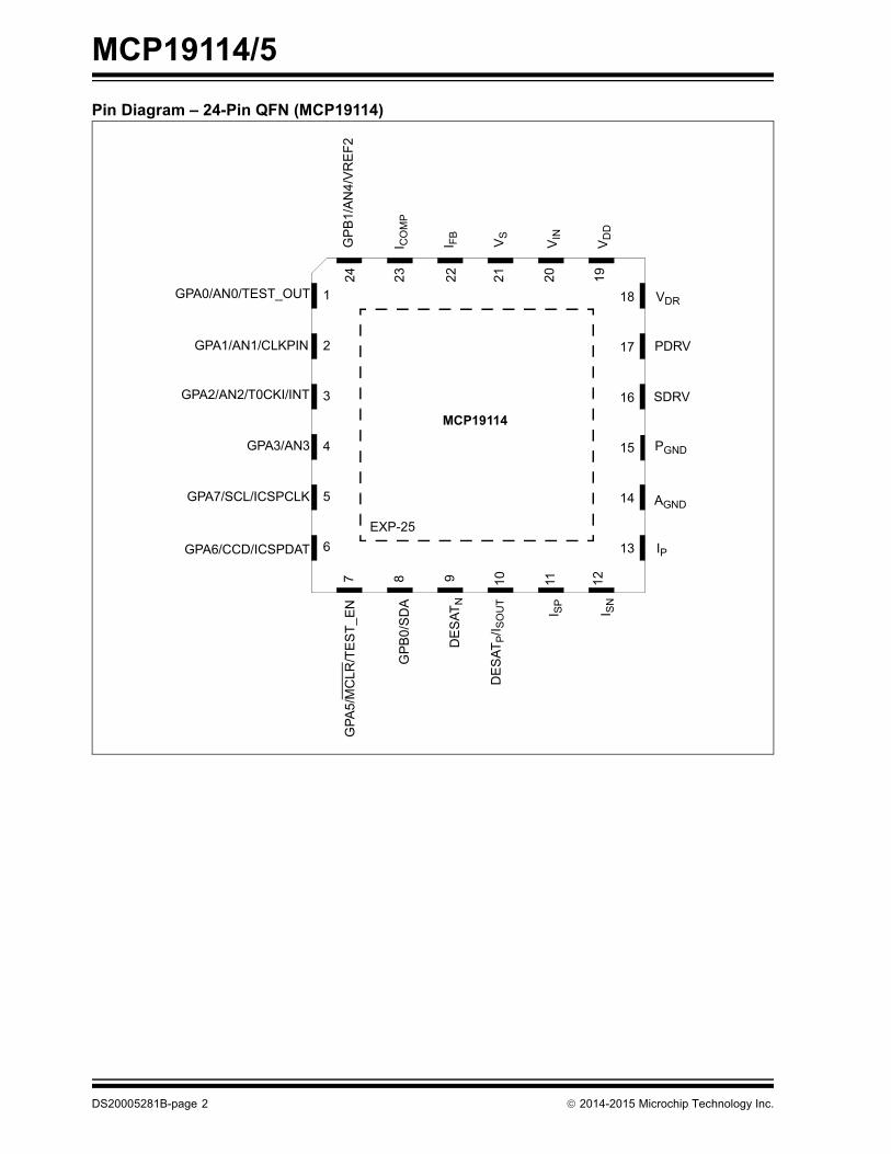
Pin Diagram – 24-Pin QFN (MCP19114)MCP19114
1
2
3
4
5
6 13
7 8 9 10 11 12
14
15
16
17
18
23 22 21 20 1924
EXP-25
GPA0/AN0/TEST_OUT
GPA1/AN1/CLKPIN
GPA2/AN2/T0CKI/INT
GPA3/AN3
GPA7/SCL/ICSPCLK
GPA6/CCD/ICSPDAT
GPA
5/M
CLR
/TE
ST_
EN
GPB
0/S
DA
DE
SAT
N
DE
SAT
P/I S
OU
T
I SP
I SN
IP
AGND
PGND
SDRV
PDRV
VDR
GP
B1/
AN
4/V
RE
F2
I CO
MP
I FB
VS
VIN
VD
D
DS20005281B-page 2
2014-2015 Microchip Technology Inc.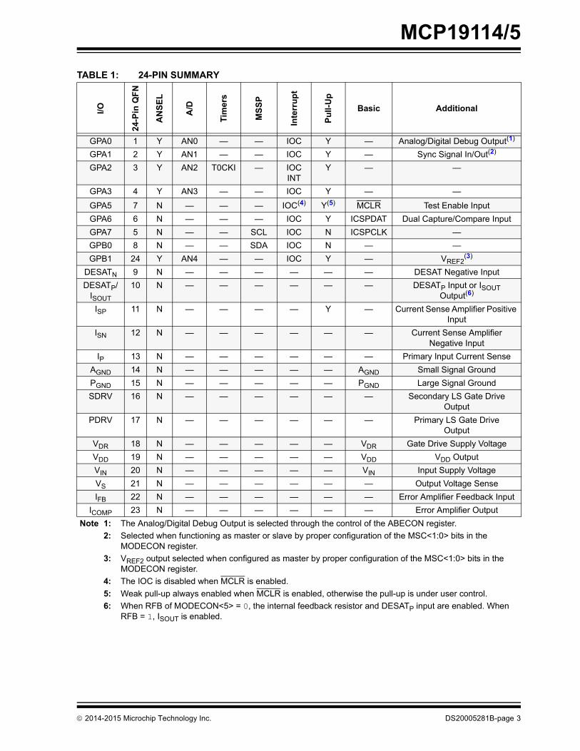
MCP19114/5
TABLE 1: 24-PIN SUMMARY
I/O
24-P
in Q
FN
AN
SEL
A/D
Tim
ers
MSS
P
Inte
rrup
t
Pull-
Up
Basic Additional
GPA0 1 Y AN0 — — IOC Y — Analog/Digital Debug Output(1)
GPA1 2 Y AN1 — — IOC Y — Sync Signal In/Out(2)
GPA2 3 Y AN2 T0CKI — IOCINT
Y — —
GPA3 4 Y AN3 — — IOC Y — —
GPA5 7 N — — — IOC(4) Y(5) MCLR Test Enable InputGPA6 6 N — — — IOC Y ICSPDAT Dual Capture/Compare InputGPA7 5 N — — SCL IOC N ICSPCLK —GPB0 8 N — — SDA IOC N — —GPB1 24 Y AN4 — — IOC Y — VREF2
(3)
DESATN 9 N — — — — — — DESAT Negative InputDESATP/
ISOUT
10 N — — — — — — DESATP Input or ISOUTOutput(6)
ISP 11 N — — — — Y — Current Sense Amplifier Positive Input
ISN 12 N — — — — — — Current Sense AmplifierNegative Input
IP 13 N — — — — — — Primary Input Current SenseAGND 14 N — — — — — AGND Small Signal GroundPGND 15 N — — — — — PGND Large Signal GroundSDRV 16 N — — — — — — Secondary LS Gate Drive
OutputPDRV 17 N — — — — — — Primary LS Gate Drive
OutputVDR 18 N — — — — — VDR Gate Drive Supply VoltageVDD 19 N — — — — — VDD VDD OutputVIN 20 N — — — — — VIN Input Supply VoltageVS 21 N — — — — — — Output Voltage SenseIFB 22 N — — — — — — Error Amplifier Feedback Input
ICOMP 23 N — — — — — — Error Amplifier OutputNote 1: The Analog/Digital Debug Output is selected through the control of the ABECON register.
2: Selected when functioning as master or slave by proper configuration of the MSC<1:0> bits in the MODECON register.
3: VREF2 output selected when configured as master by proper configuration of the MSC<1:0> bits in the MODECON register.
4: The IOC is disabled when MCLR is enabled.5: Weak pull-up always enabled when MCLR is enabled, otherwise the pull-up is under user control.6: When RFB of MODECON<5> = 0, the internal feedback resistor and DESATP input are enabled. When
RFB = 1, ISOUT is enabled.
2014-2015 Microchip Technology Inc. DS20005281B-page 3

MCP19114/5
Pin Diagram – 28-Pin QFN (MCP19115)MCP19115
1
2
3
4
5
6
7 15
8 9 10 11 12 13 14
16
17
18
19
20
21
26 25 24 23 2228 27
EXP-29
GPA1/AN1/CLKPIN
GPA2/AN2/T0CKI/INT
GPB4/AN5/ICSPDAT
GPA3/AN3
GPA7/SCL
GPA6/CCD
GPA0/AN0/TEST_OUT
GP
B6/
AN
7
GP
B5/
AN
6/IC
SPC
LK
GP
B1/
AN
4/V
RE
F2
I CO
MP
I FB VS
VIN
VDD
VDR
PDRV
SDRV
PGND
AGND
IP
GPA
5/M
CLR
/TE
ST_
EN
GPB
7/C
CD
GP
B0/
SD
A
DE
SAT
N
DE
SAT
P/I S
OU
T
I SP
I SN
DS20005281B-page 4
2014-2015 Microchip Technology Inc.
MCP19114/5
TABLE 2: 28-PIN SUMMARY
I/O
28-P
in Q
FN
AN
SEL
A/D
Tim
ers
MSS
P
Inte
rrup
t
Pull-
Up
Basic Additional
GPA0 1 Y AN0 — — IOC Y — Analog/Digital Debug Output(1)
GPA1 2 Y AN1 — — IOC Y — Sync Signal In/Out(2)
GPA2 3 Y AN2 T0CKI — IOCINT
Y — —
GPA3 5 Y AN3 — — IOC Y — —
GPA5 8 N — — — IOC(4) Y(5) MCLR Test Enable InputGPA6 7 N — — — IOC Y — Dual Capture/Single
Compare1 InputGPA7 6 N — — SCL IOC N — —GPB0 10 N — — SDA IOC N — —GPB1 26 Y AN4 — — IOC Y — VREF2
(3)
GPB4 4 Y AN5 — — IOC Y ICSPDAT —GPB5 27 Y AN6 — — IOC Y ICSPCLK —GPB6 28 Y AN7 — — IOC Y — —GPB7 9 Y — — — IOC Y — Single Compare2 Input
DESATP/ISOUT
12 N — — — — — — DESATP input or ISOUTOutput(6)
DESATN 11 N — — — — — — DESAT Negative InputISP 13 N — — — — Y — Current Sense Amplifier
Noninverting InputISN 14 N — — — — — — Current Sense Amplifier
Inverting InputIP 15 N — — — — — — Primary Input Current Sense
AGND 16 N — — — — — AGND Small Signal GroundPGND 17 N — — — — — PGND Large Signal GroundSDRV 18 N — — — — — — Secondary LS Gate Drive
OutputPDRV 19 N — — — — — — Primary LS Gate Drive OutputVDR 20 N — — — — — VDR Gate Drive Supply VoltageVDD 21 N — — — — — VDD VDD OutputVIN 22 N — — — — — VIN Input Supply VoltageVS 23 N — — — — — — Output Voltage SenseIFB 24 N — — — — — — Error Amplifier Feedback input
ICOMP 25 N — — — — — — Error Amplifier OutputNote 1: The Analog/Digital Debug Output is selected through the control of the ABECON register.
2: Selected when functioning as master or slave by proper configuration of the MSC<1:0> bits in the MODECON register.
3: VREF2 output selected when configured as master by proper configuration of the MSC<1:0> bits in the MODECON register.
4: The IOC is disabled when MCLR is enabled.5: Weak pull-up always enabled when MCLR is enabled, otherwise the pull-up is under user control.6: When RFB of MODECON<6> = 0, the internal feedback resistor is enabled allow with DESATP input.
When RFB = 1, ISOUT is enabled.
2014-2015 Microchip Technology Inc. DS20005281B-page 5
MCP19114/5
Table of Contents1.0 Device Overview .......................................................................................................................................................................... 92.0 Pin Description ........................................................................................................................................................................... 133.0 Functional Description................................................................................................................................................................ 194.0 Electrical Characteristics ............................................................................................................................................................ 225.0 Digital Electrical Characteristics ................................................................................................................................................. 296.0 Configuring the MCP19114/5 ..................................................................................................................................................... 377.0 Typical Performance Curves ...................................................................................................................................................... 538.0 System Bench Testing................................................................................................................................................................ 579.0 Device Calibration ...................................................................................................................................................................... 5910.0 Memory Organization ................................................................................................................................................................. 6911.0 Device Configuration .................................................................................................................................................................. 8112.0 Oscillator Modes......................................................................................................................................................................... 8313.0 Resets ........................................................................................................................................................................................ 8514.0 Interrupts .................................................................................................................................................................................... 9315.0 Power-Down Mode (Sleep) ...................................................................................................................................................... 10116.0 Watchdog Timer (WDT)............................................................................................................................................................ 10317.0 Flash Program Memory Control ............................................................................................................................................... 10518.0 I/O Ports .................................................................................................................................................................................... 11119.0 Interrupt-On-Change ................................................................................................................................................................ 12120.0 Internal Temperature Indicator Module..................................................................................................................................... 12521.0 Analog-to-Digital Converter (ADC) Module .............................................................................................................................. 12722.0 Timer0 Module.......................................................................................................................................................................... 13723.0 Timer1 Module with Gate Control ............................................................................................................................................. 13924.0 Timer2 Module.......................................................................................................................................................................... 14325.0 Enhanced PWM Module........................................................................................................................................................... 14526.0 Dual Capture/Compare (CCD) Module..................................................................................................................................... 14927.0 PWM Control Logic .................................................................................................................................................................. 15328.0 Master Synchronous Serial Port (MSSP) Module .................................................................................................................... 15529.0 Instruction Set Summary .......................................................................................................................................................... 19930.0 In-Circuit Serial Programming™ (ICSP™) ............................................................................................................................... 20931.0 Development Support................................................................................................................................................................21132.0 Packaging Information.............................................................................................................................................................. 215Appendix A: Revision History............................................................................................................................................................. 221Index .................................................................................................................................................................................................. 223The Microchip Web Site ..................................................................................................................................................................... 229Customer Change Notification Service .............................................................................................................................................. 229Customer Support .............................................................................................................................................................................. 229Product Identification System............................................................................................................................................................. 231DS20005281B-page 6 2014-2015 Microchip Technology Inc.

MCP19114/5
TO OUR VALUED CUSTOMERSIt is our intention to provide our valued customers with the best documentation possible to ensure successful use of your Microchipproducts. To this end, we will continue to improve our publications to better suit your needs. Our publications will be refined andenhanced as new volumes and updates are introduced. If you have any questions or comments regarding this publication, please contact the Marketing Communications Department viaE-mail at [email protected]. We welcome your feedback.
Most Current Data SheetTo obtain the most up-to-date version of this data sheet, please register at our Worldwide Web site at:
http://www.microchip.comYou can determine the version of a data sheet by examining its literature number found on the bottom outside corner of any page.The last character of the literature number is the version number, (e.g., DS30000000A is version A of document DS30000000).
ErrataAn errata sheet, describing minor operational differences from the data sheet and recommended workarounds, may exist for currentdevices. As device/documentation issues become known to us, we will publish an errata sheet. The errata will specify the revisionof silicon and revision of document to which it applies.To determine if an errata sheet exists for a particular device, please check with one of the following:• Microchip’s Worldwide Web site; http://www.microchip.com• Your local Microchip sales office (see last page)When contacting a sales office, please specify which device, revision of silicon and data sheet (include literature number) you areusing.
Customer Notification SystemRegister on our web site at www.microchip.com to receive the most current information on all of our products.
2014-2015 Microchip Technology Inc. DS20005281B-page 7

MCP19114/5
NOTES:DS20005281B-page 8
2014-2015 Microchip Technology Inc.
MCP19114/5
1.0 DEVICE OVERVIEWThe MCP19114/5 are highly integrated, mixed-signallow-side synchronous controllers that operate from4.5V to 42V. The family features an analog PWMcontroller with an integrated microcontroller core usedfor LED lighting systems, battery chargers and otherlow-side switch PWM applications. The devices featurean analog internal PWM controller similar to theMCP1631, and a standard PIC® microcontroller similarto the PIC12F617.
Complete customization of device operatingparameters, start-up or shutdown profiles, protectionlevels and fault handling procedures are accomplishedby setting digital registers using Microchip’s MPLAB® XIntegrated Development Environment software andone of Microchip’s many in-circuit debugger and deviceprogrammers.
The MCP19114/5 mixed-signal low-side synchronouscontrollers feature integrated programmable inputUVLO/OVLO, programmable output overvoltage (OV),two low-side gate drive outputs with independentprogrammable dead time, programmable leading edgeblanking (four steps), programmable 6-bit slopecompensation and an integrated internalprogrammable oscillator for fixed-frequencyapplications. An integrated 8-bit reference voltage(VREF) is used for setting output voltage or current. Aninternal comparator supports quasi-resonantapplications. Additional Capture and Comparemodules are integrated for additional control, includingenhanced dimming capability. The MCP19114/5devices contain two internal LDOs. A 5V LDO is usedto power the internal processor and provide 5Vexternally. This 5V external output can be used tosupply the gate drive. An analog filter between the VDDoutput and the VDR input is recommended whenimplementing a 5V gate drive supplied from VDD. Two4.7 µF capacitors are recommended with one placedas close as possible to VDD and one as close aspossible to VDR, separated by a 10 isolation resistor.DO NOT exceed 10 µF on the VDD. An external supplyis required to implement higher gate drive voltages. Byutilizing Microchip’s TC1240A voltage doubler suppliedfrom VDD to provide VDR, a 10V gate drive can beachieved. A 4V LDO is used to power the internalanalog circuitry. The two low-side drivers can be usedto operate the power converter in bidirectional mode,enabling the “shaping” of LED dimming current in LEDapplications or developing bidirectional powerconverters for battery-powered applications.
The MCP19114 is packaged in a 24-lead4 mm x 4 mm QFN and offers an alternate-bonded28-lead 5 mm x 5 mm QFN. The MCP19115 ispackaged in a 28-lead 5 mm x 5 mm QFN.
2014-2015 Microchip Technology Inc.
The ability for system designers to configureapplication-specific features allows the MCP19114/5 tobe offered in smaller packages than currently availablein integrated devices today. The General PurposeInput/Output (GPIO) of the MCP19114/5 can beconfigured to offer a status output; a device enable, tocontrol an external switch; a switching frequencysynchronization output or input or even a device statusor "heartbeat" indicator. This flexibility allows theMCP19114/5 packages and complete solutions to besmaller, thereby saving size and cost of the systemprinted circuit boards.
With integrated features like output current adjustmentand dynamic output voltage positioning, theMCP19114/5 family has the best in-class performanceand highest integration level currently available.
Power trains supported by this architecture include butare not limited to boost, flyback, quasi-resonantflyback, SEPIC, Ćuk, etc. Two low-side gate drivers arecapable of sinking and sourcing 1A at 10V VDR. With a5V gate drive, the driver is capable of 0.5A sink andsource. The user has the option to allow the VIN UVLOto shut down the drivers by setting the UVLOEN bit.When this bit is not set, the device drivers will ridethrough the UVLO condition and continue to operateuntil VDR reaches the gate drive UVLO value. Thisvalue is selectable at 2.7V or 5.4V and is alwaysenabled. An internal reset for the microcontroller coreis set to 2.0V. An internal comparator module is used tosense the desaturation of the flyback transformer tosynchronize switching for quasi-resonant applications.The operating input voltage for normal device operationranges from 4.5V to 42V with an absolute maximum of44V. The maximum transient voltage is 48V for 500 ms.An I2C serial bus is used for device communicationsfrom the PWM controller to the system.
DS20005281B-page 9
MC
P19114/5
DS
20005281B-page 10
2014-2015 M
icrochip Technology Inc.
VIN
V
V
ATN
ATP
O
O
D
VVDD VVDD
4.5V to 42V
μF
4.7 μF
10Ω
lace recommended VVDD and VDR 4.7 μFapacitors as close to respective pins as possible
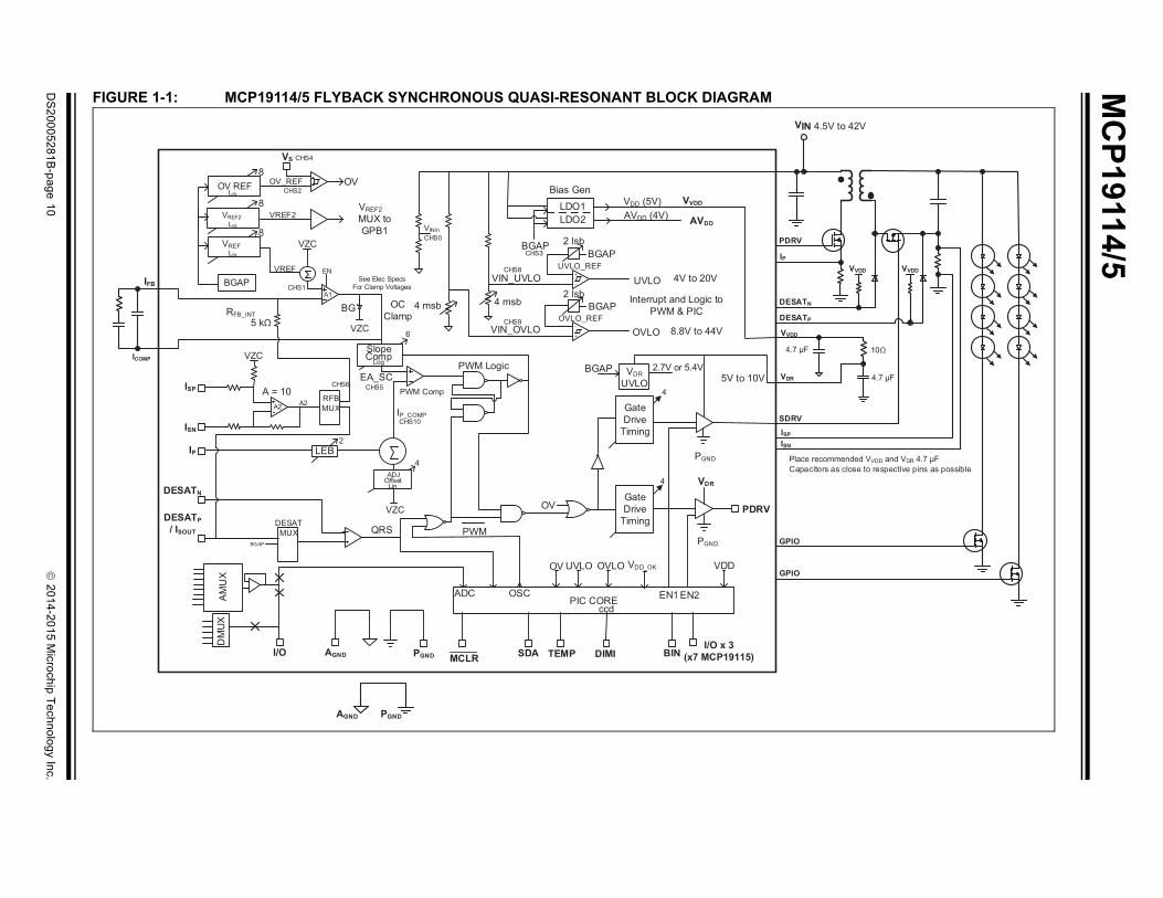
FIGURE 1-1: MCP19114/5 FLYBACK SYNCHRONOUS QUASI-RESONANT BLOCK DIAGRAM
VDD (5V)
BGAP
UVLO
VREF
OV REF
8
8OV
BGAP
PIC COREOSC
OV UVLO
PDRV
ISN
A = 10
IP LEB2
EA_SCPWM Comp
PWM Logic
DESATN
QRS
VDR
AGND MCLR DIMISDA TEMP
VS
BINI/O x 3
(x7 MCP19115)
OV
OCClamp
6
ccd
4
4
EN1 EN2
OVLO
4
IFB
PGND
PGND
PGND
VVDDVREF2MUX to GPB1
I/O
LDO1LDO2
Bias Gen
AVDD (4V) AVDD
VDD
VREF2
8
DESATMUX
4V to 20V
8.8V to 44V
EN
BGAP
DESATP/ ISOUT
ISP
VDD_OK
RFBMUX
BG5 kΩ
GateDrive
Timing
GateDrive
Timing
IP_COMPA2
A1
OV_REF
VREF2
VREF
A2
OVLO_REF
UVLO_REF
LIN
Interrupt and Logic to PWM & PIC
LIN
LIN
RFB_INT
AM
UX
5V to 10V
4 msb
VIN_UVLO
Log
Lin
SlopeComp
ADJOffset
VIN_OVLO
+
-
-
+ OVLO
DM
UX
PWM
VZC
VZC
VZC
VZC
VDR
UVLOBGAP 2.7V or 5.4V
ADC
4 msb
2 lsb
2 lsb
BGAP
BGAP
CHS1
CHS2
CHS3
CHS4
CHS5CHS6
CHS8
CHS9
CHS10
See Elec SpecsFor Clamp Voltages
PDR
IP
SDR
DES
DES
ISN
ISP
GPI
GPI
AGND PGND
VVD
VDR
ICOMP4.7
PC
CHS0VIN/n

MCP19114/5
FIGURE 1-2: MCP19114 ĆUK SYNCHRONOUS POSITIVE OUTPUT APPLICATION DIAGRAMFIGURE 1-3: MCP19114 BOOST QUASI-RESONANT APPLICATION DIAGRAM
VIN
VDR
ISP
PGND
VS
IP
VIN
PDRV
BIN
DIMI
DESATN
MCLR
CCD
MCP19114
ICOMP
I/OTEMP SNS
EN
2
SDRV
AGND
VDD
IFB4x4
24Ld
QFN
VDD
I/O I/O
I/O
2
VDD
5V
DESATP
ISN
I/O
TC1240VOLTAGEDOUBLER
10V
VIN
VDR
ISP
PGND
VS
IP
VIN
PDRV
BIN
DIMI
DESATN
MCLR
CCD
MCP19114
ISN
ICOMPI/OTEMP SNS
EN
AGND
VDD
ISOUT
IFB
4x4
24Ld
QFN
VDD
I/O
VDD
5V
2
SW1 SW2
DESATN
DESATN
DESATP DESATP
DESATP
SDRV
SW1
SW2
I/O
I/O
2
2014-2015 Microchip Technology Inc. DS20005281B-page 11

MCP19114/5
FIGURE 1-4: MICROCONTROLLER CORE BLOCK DIAGRAMFlash
ProgramMemory
13 Data Bus 8
14ProgramBus
Instruction reg.
Program Counter
RAM
FileRegisters
Direct Addr 7
RAM Addr 9
Addr MUX
IndirectAddr
FSR reg.
STATUS reg.
MUX
ALU
W reg
InstructionDecode &
Control
TimingGenerationTESTCLKIN
PORTGPA
8
8
8
3
8 Level Stack 256
4K x 14
bytes(13-bit)
Power-UpTimer
Power-OnReset
WatchdogTimer
MCLR VIN VSS
Timer0 Timer1T0CKI
Configuration
8 MHz InternalOscillator
Timer2
I2C™
GPA0GPA1GPA2GPA3
GPA5
Analog Interface
SDASCL
PMDATL
EEADDR
Self read/ write flashmemory
Registers
PORTGPB
GPB0GPB1
GPB6 (MCP19115)
GPB4 (MCP19115)
PWM
GPB5 (MCP19115)
GPA6GPA7
GPB7 (MCP19115)
EnhancedCCD
GPA6 GPB7 (MCP19115)
DS20005281B-page 12
2014-2015 Microchip Technology Inc.
MCP19114/5
2.0 PIN DESCRIPTIONThe 24-lead MCP19114 and 28-lead MCP19115devices feature pins that have multiple functionsassociated with each pin. Table 2-1 provides adescription of the different functions. Refer toSection 2.1 “Detailed Pin Functional Description”for more detailed information.
2014-2015 Microchip Technology Inc.
TABLE 2-1: MCP19114/5 PINOUT DESCRIPTION
Name Function Input Type
Output Type Description
GPA0/AN0/TEST_OUT GPA0 TTL CMOS General-purpose I/OAN0 AN — A/D Channel 0 input
TEST_OUT — — Internal analog/digital signal multiplexer output(1)
GPA1/AN1/CLKPIN GPA1 TTL CMOS General-purpose I/OAN1 AN — A/D Channel 1 input
CLKPIN ST CMOS Switching frequency clock input or output(2)
GPA2/AN2/T0CKI/INT GPA2 ST CMOS General-purpose I/OAN2 AN — A/D Channel 2 input
T0CKI ST — Timer0 clock inputINT ST — External interrupt
GPA3/AN3 GPA3 TTL CMOS General-purpose I/OAN3 AN — A/D Channel 3 input
GPA5/MCLR GPA5 TTL — General-purpose input only
MCLR ST — Master Clear with internal pull-upGPA6/CCD/ICSPDAT GPA6 ST CMOS General-purpose I/O
ICSPDAT ST CMOS Serial Programming Data I/OCCD ST CMOS Single Compare output. Dual Capture input
GPA7/SCL/ICSPCLK GPA7 ST OD General-purpose open drain I/OSCL I2C™ OD I2C clock
ICSPCLK ST — Serial Programming ClockGPB0/SDA GPB0 TTL OD General-purpose I/O
SDA I2C™ OD I2C data input/outputGPB1/AN4/VREF2 GPB1 TTL CMOS General-purpose I/O
AN4 AN — A/D Channel 4 inputVREF2 — AN VREF2 DAC Output(3)
GPB4/AN5/ICSPDAT(MCP19115 Only)
GPB4 TTL CMOS General-purpose I/OAN5 AN — A/D Channel 5 input
ICSPDAT ST CMOS Primary Serial Programming Data I/OGPB5/AN6/ICSPCLK(MCP19115 Only)
GPB5 TTL CMOS General-purpose I/OAN6 AN — A/D Channel 6 input
ISCPCLK ST — Primary Serial Programming ClockLegend: AN = Analog input or output CMOS = CMOS compatible input or output OD = Open-Drain
TTL = TTL compatible input ST = Schmitt Trigger input with CMOS levels I2C = Schmitt Trigger input with I2CNote 1: The Analog/Digital Debug Output is selected through the control of the ABECON register.
2: Selected when functioning as master or slave by proper configuration of the MSC<1:0> bits in the MODECON register.3: VREF2 output selected when configured as master by proper configuration of the MSC<1:0> bits in the MODECON
register.
DS20005281B-page 13
MCP19114/5
GPB6/AN7(MCP19115 Only)
GPB6 TTL CMOS General-purpose I/OAN7 AN — A/D Channel 7 input
GPB7/CCD(MCP19115 Only)
GPB7 TTL CMOS General-purpose I/OCCD ST CMOS Single Compare output. Dual Capture input.
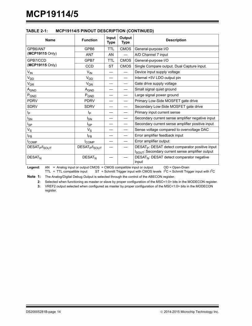
VIN VIN — — Device input supply voltageVDD VDD — — Internal +5V LDO output pinVDR VDR — — Gate drive supply voltageAGND AGND — — Small signal quiet groundPGND PGND — — Large signal power groundPDRV PDRV — — Primary Low-Side MOSFET gate driveSDRV SDRV — — Secondary Low-Side MOSFET gate driveIP IP — — Primary input current senseISN ISN — — Secondary current sense amplifier negative inputISP ISP — — Secondary current sense amplifier positive inputVS VS — — Sense voltage compared to overvoltage DACIFB IFB — — Error amplifier feedback inputICOMP ICOMP — — Error amplifier outputDESATP/ISOUT DESATP/ISOUT — — DESATP: DESAT detect comparator positive input
ISOUT: Secondary current sense amplifier outputDESATN DESATN — — DESATN: DESAT detect comparator negative
input
TABLE 2-1: MCP19114/5 PINOUT DESCRIPTION (CONTINUED)
Name Function Input Type
Output Type Description
Legend: AN = Analog input or output CMOS = CMOS compatible input or output OD = Open-DrainTTL = TTL compatible input ST = Schmitt Trigger input with CMOS levels I2C = Schmitt Trigger input with I2C
Note 1: The Analog/Digital Debug Output is selected through the control of the ABECON register.2: Selected when functioning as master or slave by proper configuration of the MSC<1:0> bits in the MODECON register.3: VREF2 output selected when configured as master by proper configuration of the MSC<1:0> bits in the MODECON
register.
DS20005281B-page 14 2014-2015 Microchip Technology Inc.

MCP19114/5
2.1 Detailed Pin FunctionalDescription
2.1.1 GPA0 PINGPA0 is a general-purpose TTL input or CMOS outputpin whose data direction is controlled in TRISGPA. Aninternal weak pull-up and interrupt-on-change are alsoavailable.
AN0 is an input to the A/D. To configure this pin to beread by the A/D on channel 0, bits TRISA0 and ANSA0must be set.
The ABECON register can be configured to set this pinto the TEST_OUT function. It is a buffered output of theinternal analog or digital signal multiplexers. Analogsignals present on this pin are controlled by theADCON0 register. Digital signals present on this pinare controlled by the ABECON register.
2.1.2 GPA1 PINGPA1 is a general-purpose TTL input or CMOS outputpin whose data direction is controlled in TRISGPA. Aninternal weak pull-up and interrupt-on-change are alsoavailable.
AN1 is an input to the A/D. To configure this pin to beread by the A/D on channel 1, bits TRISA1 and ANSA1must be set.
When the MCP19114/5 are configured as a master orslave, this pin is configured to be the switchingfrequency synchronization input or output (CLKPIN).
2.1.3 GPA2 PINGPA2 is a general-purpose ST input or CMOS outputpin whose data direction is controlled in TRISGPA. Aninternal weak pull-up and interrupt-on-change are alsoavailable.
AN2 is an input to the A/D. To configure this pin to beread by the A/D on channel 2, bits TRISA2 and ANSA2must be set.
When bit T0CS is set in the OPTION_REG register, theT0CKI function is enabled. Refer to Section 22.0“Timer0 Module” for more information.
GPA2 can also be configured as an external interruptby setting the INTE bit. Refer to Section 14.2“GPA2/INT Interrupt” for more information.
2.1.4 GPA3 PINGPA3 is a general-purpose TTL input or CMOS outputpin whose data direction is controlled in TRISGPA. Aninternal weak pull-up and interrupt-on-change are alsoavailable.
AN3 is an input to the A/D. To configure this pin to beread by the A/D on channel 3, bits TRISA3 and ANSA3must be set.
2014-2015 Microchip Technology Inc.
2.1.5 GPA5 PINGPA5 is a general-purpose TTL input only pin. Aninternal weak pull-up and interrupt-on-change are alsoavailable.
For programming purposes, this pin is to be connectedto the MCLR pin of the serial programmer. Refer toSection 30.0 “In-Circuit Serial Programming™(ICSP™)” for more information.
This pin is MCLR when the MCLRE bit is set in theCONFIG register.
2.1.6 GPA6 PINGPA6 is a general-purpose CMOS output ST input pinwhose data direction is controlled in TRISGPA.
ICSPDAT is a serial programming data I/O function.This can be used in conjunction with ICSPCLK to serialprogram the device.
GPA6 is part of the CCD Module. For more information,refer to Section 26.0 “Dual Capture/Compare (CCD)Module”.
2.1.7 GPA7 PINGPA7 is a true open drain general-purpose pin whosedata direction is controlled in TRISGPA. There is nointernal connection between this pin and device VDD.This pin does not have a weak pull-up, but inter-rupt-on-change is available.
This pin is the primary ICSPCLK input. This can beused in conjunction with ICSPDAT to serial programthe device.
When the MCP19114/5 is configured for I2Ccommunication, Section 28.2 “I2C Mode Overview”,GPA7 functions as the I2C clock (SCL). This pin mustbe configured as an input to allow proper operation.
DS20005281B-page 15

MCP19114/5
2.1.8 GPB0 PINGPB0 is a true open-drain general-purpose pin whosedata direction is controlled in TRISGPB. There is nointernal connection between this pin and device VDD.This pin does not have a weak pull-up, butinterrupt-on-change is available. When theMCP19114/5 are configured for I2C communication,Section 28.2 “I2C Mode Overview”, GPB0 functionsas the I2C clock (SDA). This pin must be configured asan input to allow proper operation.2.1.9 GPB1 PINGPB1 is a general-purpose TTL input or CMOS outputpin whose data direction is controlled in TRISGPB. Aninternal weak pull-up and interrupt-on-change are alsoavailable.
AN4 is an input to the A/D. To configure this pin to beread by the A/D on channel 4, bits TRISB1 and ANSB1must be set.
When the MCP19114/5 are configured as a master, thispin is configured to be the VREF2 DAC output.
2.1.10 GPB4 PIN (MCP19115 ONLY)GPB4 is a general-purpose TTL input or CMOS outputpin whose data direction is controlled in TRISGPB. Aninternal weak pull-up and interrupt-on-change are alsoavailable.
AN5 is an input to the A/D. To configure this pin to beread by the A/D on channel 5, bits TRISB4 and ANSB4must be set.
ICSPDAT is the primary serial programming data I/Ofunction. This is used in conjunction with ICSPCLK toserial program the device.
2.1.11 GPB5 PIN (MCP19115 ONLY)GPB5 is a general-purpose TTL input or CMOS outputpin whose data direction is controlled in TRISGPB. Aninternal weak pull-up and interrupt-on-change are alsoavailable.
AN6 is an input to the A/D. To configure this pin to beread by the A/D on channel 6, bits TRISB5 and ANSB5must be set.
ICSPCLK is the primary serial programming clockfunction. This is used in conjunction with ICSPDAT toserial program the device.
2.1.12 GPB6 PIN (MCP19115 ONLY)GPB6 is a general-purpose TTL input or CMOS outputpin whose data direction is controlled in TRISGPB. Aninternal weak pull-up and interrupt-on-change are alsoavailable.
AN7 is an input to the A/D. To configure this pin to beread by the A/D on channel 7, bits TRISB6 and ANSB6must be set.
DS20005281B-page 16
2.1.13 GPB7 PIN (MCP19115 ONLY)GPB7 is a general-purpose TTL input or CMOS outputpin whose data direction is controlled in TRISGPB. Aninternal weak pull-up and interrupt-on-change are alsoavailable.
GPB7 is part of the CCD Module. For more information,refer to Section 26.0 “Dual Capture/Compare (CCD)Module”.
2.1.14 DESATN PINInternal comparator inverting input. Used duringquasi-resonant operation for desaturation detection.
2.1.15 DESATP/ISOUT PINWhen using the internal comparator for desaturationdetection during quasi-resonant operation, this pinconnects to the comparator’s noninverting input. Theoutput of the remote sense current sense amplifier getsconfigured to utilize the 5 k internal feedback resistor.When not utilizing the internal comparator and notconfigured to use the 5 k internal feedback resistor,the current sense amplifier gets connected to this pinand is ISOUT.
2.1.16 ISP PINThe noninverting input to internal current senseamplifier, typically used to differentially remote sensesecondary current. This pin can be internally pulled-upto VDD by setting the <ISPUEN> bit in the PE1 register.
2.1.17 ISN PINThe inverting input to internal current sense amplifier,typically used to differentially remote sense secondarycurrent.
2.1.18 IP PINPrimary input current sense for current mode controland peak current limit. For voltage mode control, thispin can be connected to an artificial ramp.
2.1.19 AGND PINAGND is the small signal ground connection pin. Thispin should be connected to the exposed pad on thebottom of the package.
2.1.20 PGND PINConnect all large signal level ground returns to PGND.These large-signal level ground traces should have asmall loop area and minimal length to prevent couplingof switching noise to sensitive traces.
2014-2015 Microchip Technology Inc.
MCP19114/5
2.1.21 SDRV PINThe gate of the low-side secondary MOSFET isconnected to SDRV. The PCB trace connecting SDRVto the gate must be of minimal length and appropriatewidth to handle the high-peak drive current and fastvoltage transitions.2.1.22 PDRV PINThe gate of the low-side primary MOSFET isconnected to PDRV. The PCB tracing connectingPDRV to the gate must be of minimal length andappropriate width to handle the high-peak drivecurrents and fast voltage transitions.
2.1.23 VDR PINThe supply for the low-side drivers is connected to thispin and has an absolute maximum rating of +13.5V.This pin can be connected by an RC filter to the VDDpin.
2.1.24 VDD PINThe output of the internal +5.0V regulator is connectedto this pin. It is recommended that a 1.0 µF minimum/10 µF maximum bypass capacitor be connectedbetween this pin and the GND pin of the device. Thebypass capacitor should be physically placed close tothe device.
2.1.25 VIN PINInput power connection pin of the device. It isrecommended that capacitance be placed between thispin and the GND pin of the device.
2.1.26 VS PINAnalog input connected to the noninverting input of theovervoltage comparator. Typically used as outputvoltage overvoltage protection. The inverting input ofthe overvoltage comparator is controlled by the OVREF DAC.
2.1.27 IFB PINError amplifier inverting feedback connection.
2.1.28 ICOMP PINError amplifier output signal.
2.1.29 EXPOSED PAD (EP)It is recommended to connect the exposed pad toAGND.
2014-2015 Microchip Technology Inc.
Note: Upon initial power-up, the device may applya weak pull-up effect on GPIO pads thatcan be configured as analog inputs. Oncethe external capacitance on the 5V (VDD) ischarged and the external 5V regulatorexceeds the internal 4V regulator (AVDD)the pull-up effect is shut off. To prevent thisparasitic power-up effect, a pull-down resis-tor of 10 kΩ maximum is recommended forGPIO with analog input capability. Thisapplies to GPA0, GPA1, GPA2, GPA3,GPB1, GPB4 (MCP19115 only), GPBD(MCP19115 only), GPB6 (MCP19115 only).
DS20005281B-page 17

MCP19114/5
NOTES:DS20005281B-page 18
2014-2015 Microchip Technology Inc.
MCP19114/5
3.0 FUNCTIONAL DESCRIPTION
3.1 Linear RegulatorsThe operating input voltage for the MCP19114/5ranges from 4.5V to 42V. There are two internal LowDropout (LDO) voltage regulators. A 5V LDO is used topower the internal processor and provide a 5V outputfor external usage. A second LDO (AVDD) is a 4Vregulator and is used to power the remaining analoginternal circuitry. Using an LDO to power theMCP19114/5, the input voltage is monitored using aresistor divider. The MCP19114/5 also incorporatebrown-out protection. Refer to Section 13.3“Brown-Out Reset (BOR)” for details. The PIC corewill reset at 2.0V VDD.
3.2 Output Drive CircuitryThe MCP19114/5 integrate two low-side drivers usedto drive the external low-side N-Channel powerMOSFETs for synchronous applications, such assynchronous flyback and synchronous Ćuk converters.Both converter types can be configured fornonsynchronous control by replacing the synchronousFET with a diode. The flyback is also capable ofquasi-resonant operation. The MCP19114/5 can alsobe configured as a Boost or SEPIC switch-mode powersupply (SMPS). In Boost mode, nonsynchronousfixed-frequency or nonsynchronous quasi-resonantcontrol can be utilized. This device can also be used asa SEPIC SMPS in fixed-frequency nonsynchronousmode. The low-side drive is capable of switching theMOSFET at high frequency in typical SMPSapplications. The gate drive (VDR) can be supplied from5V to 10V. The drive strength is capable of up to 1Asink/source with 10V gate drive and down to 0.5Asink/source with 5V gate drive. A programmable delayis used to set the gate turn-on dead time. This preventsoverlap and shoot-through currents that can decreasethe converter efficiency. Each driver shall have its ownEN input controlled by the microcontroller core.
3.3 Current SenseThe output current is differentially sensed by theMCP19114/5. In low-current applications, this helpsmaintain high system efficiency by minimizing powerdissipation in current sense resistors. Differentialcurrent sensing also minimizes external ground shifterrors. The internal differential amplifier has a typicalgain of 10 V/V.
2014-2015 Microchip Technology Inc.
3.4 Peak Current Mode The MCP19114/5 is a peak current mode controlleddevice with the current sensing element in series withthe primary side MOSFET. Programmable leadingedge blanking can be implemented to blank currentspikes resulting from turn on. The blank time iscontrolled from the ICLEBCON register.
Primary input current offset adjust is also available viauser programmability, thus limiting peak primary inputcurrent. This offset adjustment is controlled by theICOACON register.
3.5 Magnetic Desaturation DetectionAn internal comparator module is used to detect powertrain magnetic desaturation for quasi-resonantapplications. The comparator output is used as a signalto synchronize the start of the next switching cycle.This operation differs from the traditionalfixed-frequency application. The DESAT comparatoroutput can be enabled and routed into the PWMcircuitry or disabled for fixed-frequency applications.During Quasi-Resonant (QR) operation, the DESATcomparator output is enabled and combined with a pairof one-shot timers and a flip-flop to sustain PWMoperation. Timer2 (TMR2) must be initialized and set torun at a frequency lower than the minimum QRoperating frequency. When the CDSWDE bit is set inthe DESATCON register, TMR2 serves as a watchdog. An example of the order of events for a Flyback SMPSin synchronous QR operation is as follows:The primary gate drive (PDRV) goes high. The outputof the DESAT comparator is high. The primary currentincreases until IP reaches the level of the Error Ampand causes PWM comparator output to go low. ThePDRV goes low and the secondary gate drive (SDRV)goes high (after programmed dead time). This triggersthe first one-shot to send a 200 ns pulse that resets theflip-flop and TMR2 (WDM_RESET). The 200 nsone-shot pulse design is implemented to mask out anyspurious transitions at the DESAT comparator outputcaused by switching noise. The SDRV stays high untilthe secondary winding completely runs out of energy,at which time the output capacitance begins to sourcecurrent back through the winding and secondaryMOSFET. The DESAT comparator detects this and itsoutput goes low. This sets the flip-flop and triggers thesecond one-shot to send a 33 ns pulse to the controllogic, causing the SDRV to go low and the PDRV to gohigh (after programmed dead time). The cycle thenrepeats. If, for any reason, the reset one-shot does notfire, the WDM_RESET signal stays low and TMR2 isallowed to run until the PWM signal kicks off a newcycle.The desaturation comparator module is controlled bythe DESATCON register.
DS20005281B-page 19

MCP19114/5
3.6 Start-UpTo control the output current during start-up, theMCP19114/5 have the capability to monotonicallyincrease system current, at the user’s discretion. Thisis accomplished through the control of the referencevoltage DAC (VREF). The entire start-up profile is underuser control via software.3.7 Driver Control CircuitryThe internal driver control circuitry of the MCP19114/5is comprised of an error amplifier (EA), a high-speedcomparator and a latch similar to the MCP1631.
The error amplifier generates the control voltage usedby the high-speed PWM comparator. There is aninternally generated reference voltage, VREF. Thedifference or error between this internal referencevoltage and the actual feedback voltage is the controlvoltage. Some applications will implement parkedtimes where the gate drives are not active. Forexample, when changing between LED strings andafter voltage repositioning, the user can disable thegate drives and park the error amplifier output low.During the time when the EA is parked, its output will beclamped low (1 * BG) such that it is in a known statewhen reactivated. Before the output switches arere-enabled, it may be necessary to re-enable the EAsome time prior to enabling the output drivers. Thisprior-EA enable time will allow the EA to slew towardsthe intended target and prevent the secondary switchfrom turning on for an extensive period of time,unintentionally discharging the output capacitance andpulling the output voltage down. Externalcompensation is used to stabilize the control system.
Since the MCP19114/5 are peak current modecontrolled, the comparator compares the primary peakcurrent waveform (IP) that is based upon the currentflowing in the primary side with the error amplifiercontrol output voltage. This error amplifier controloutput voltage also has user-programmable slopecompensation subtracted from it. In fixed-frequencyapplications, the slope compensation signal isgenerated to be greater than 1/2 the down slope of theinductor current waveform and is controlled by theSLPCRCON register. Offset adjust ability is alsoavailable to set the peak current limit of the primaryswitch for overcurrent protection. The range of theslope compensation ramp is specified. When thecurrent sense signal reaches the level of the controlvoltage minus slope compensation, the on cycle isterminated and the external switch is latched off untilthe beginning of the next cycle which begins at the nextclock cycle.
To improve current regulation at low levels, a pedestalvoltage (VZC) set to the BG (1.23V) is implemented.This virtual ground serves as the reference for the erroramplifier (A1), slope compensation, current senseamplifier (A2) and the IP offset adjustment.
DS20005281B-page 20
An S-R latch (Set-Rest-Flip-Flop) is used to prevent thePWM circuitry from turning the external switch on untilthe beginning of the next clock cycle.
3.8 Fixed PWM FrequencyThe switching frequency of the MCP19114/5 while notcontrolled by the DESAT comparator output isgenerated by using a single edge of the 8 MHz internalclock. The user sets the MCP19114/5 switchingfrequency by configuring the PR2 register. Themaximum allowable PDRV duty cycle is adjustable andis controlled by the PWMRL register. Theprogrammable range of the switching frequency will be31.25 kHz to 2 MHz. The available switching frequencybelow 2 MHz is defined as FSW = 8 MHz/N, where N isa whole number between 4 N 256. Refer toSection 25.0 “Enhanced PWM Module” for details.
3.9 VREFThis reference is used to generate the voltageconnected to the noninverting input of the erroramplifier. The entire analog control loop is raised to avirtual ground pedestal equal to the Band Gap voltage(1.23V).
3.10 OV REFThis reference is used to set the output overvoltage setpoint. It is compared to the VS input pin, which istypically proportional to the output voltage based on aresistor divider. OV protection, when enabled, can beset to a value for the protection of system circuitry or itcan be used to “ripple” regulate the converter outputvoltage for repositioning purposes. For details, refer toRegister 6-4.
3.11 Independent Gate Drive with Programmable Delay
Two independent low-side gate drives are integratedfor synchronous applications. Programmable delay hasbeen implemented to improve efficiency and preventshoot-through currents. Each gate drive has anindependent enable input controlled by the PE1register and programmable dead time controlled by theDEADCON register.
2014-2015 Microchip Technology Inc.
MCP19114/5
3.12 Temperature Management3.12.1 THERMAL SHUTDOWNTo protect the MCP19114/5 from overtemperatureconditions, a 150°C junction temperature thermalshutdown has been implemented. When the junctiontemperature reaches this limit, the device disables theoutput drivers. In Shutdown mode, both PDRV andSDRV outputs are disabled and the overtemperatureflag (OTIF) is set in the PIR2 register. When thejunction temperature is reduced by 20°C to 130°C, theMCP19114/5 can resume normal output driveswitching.
3.12.2 TEMPERATURE REPORTINGThe MCP19114/5 have a second on-chip temperaturemonitoring circuit that can be read by the ADC throughthe analog test MUX. Refer to Section 20.0 “InternalTemperature Indicator Module” for details on thisinternal temperature monitoring circuit.
2014-2015 Microchip Technology Inc.
DS20005281B-page 21
MCP19114/5
4.0 ELECTRICAL CHARACTERISTICS
4.1 ABSOLUTE MAXIMUM RATINGS †
VIN - VGND (operating) .................................................................................................................................................-0.3V to +44VVIN (transient < 500 ms)............................................................................................................................................+48VPDRV ..................................................................................................................................(GND - 0.3V) to (VDR + 0.3V)SDRV ....................................................................... ..........................................................(GND - 0.3V) to (VDR + 0.3V)VDD Internally Generated ......................................... ...............................................................................................+6.5VVDR Externally Generated ........................................ .............................................................................................+13.5VVoltage on MCLR with respect to GND.................... ............................................................................... -0.3V to +13.5VMaximum voltage: any other pin .................................. ...................................................+(VGND - 0.3V) to (VDD + 0.3V)Maximum output current sunk by any single I/O pin .... ..........................................................................................25 mAMaximum output current sourced by any single I/O pin ..........................................................................................25 mAMaximum current sunk by all GPIO.............................. ..........................................................................................90 mAMaximum current sourced by all GPIO ........................ ..........................................................................................35 mAStorage Temperature.................................................... ..........................................................................-65°C to +150°CMaximum Junction Temperature .................................. ........................................................................................+150°COperating Junction Temperature.................................. ..........................................................................-40°C to +125°CESD protection on all pins (HBM)................................. ......................................................................................... 2.0 kVESD protection on all pins (MM)................................... ........................................................................................... 200V† Notice: Stresses above those listed under “Maximum Ratings” may cause permanent damage to the device. This isa stress rating only and functional operation of the device at those or any other conditions above those indicated in theoperational listings of this specification is not implied. Exposure to maximum rating conditions for extended periodsmay affect device reliability.
4.2 Electrical Characteristics
DS20005281B-page 22
Electrical Specifications: Unless otherwise noted, VIN = 12V, FSW = 150 kHz, TA = +25°C. Boldface specifications apply over the TA range of -40°C to +125°C.
Parameters Sym. Min. Typ. Max. Units Conditions
InputInput Voltage VIN 4.5 — 42 VInput QuiescentCurrent
IQ — 5 6.5 mA VIN = 12V, Not switching— 5 6.75 VIN = 20V, Not switching
Shutdown Current ISHDN— 30 150 µA VIN = 12V
(Note 1)Linear Regulator VDDInternal Circuitry Bias Voltage
VDD 4.75 5.0 5.5 V VIN = 6.0V to 42V
Maximum External VDD Output Current
IDD_OUT 35 — — mA VIN = 6.0V to 42V(Note 4)
Line Regulation VDD-OUT/(VDD-OUT * VIN)
-0.1 0.002 0.1 %/V (VDD + 1.0V) VIN 20V(Note 4)
Load Regulation VDD-OUT/VDD-OUT
-0.65 0.1 +0.65 % IDD_OUT = 1 mA to 20 mA(Note 4)
Output Short-Circuit Current
IDD_SC — 50 — mA VIN = (VDD + 1.0V)(Note 4)
Note 1: Refer to Section 15.0 “Power-Down Mode (Sleep)”.2: These parameters are characterized, but not production tested.3: Ensured by design, not production tested.4: VDD is the voltage present at the VDD pin.5: Dropout voltage is defined as the input-to-output voltage differential at which the output voltage drops 2% below its
nominal value measured at a 1V differential between VIN and VDD.6: The VDD LDO will limit the total source current to a maximum of 35 mA. Individually each pin can source a
maximum of 15 mA.
2014-2015 Microchip Technology Inc.
MCP19114/5
Dropout Voltage VIN - VDD — 0.3 0.5 V IDD_OUT = 20 mA,(Notes 4 and 5)
Power Supply Rejection Ratio
PSRRLDO — 60 — dB f 1000 Hz,IDD_OUT = 25 mACIN = 0 µF, CDD = 1 µF
Linear Regulator AVDDInternal Analog Supply Voltage
AVDD — 4.0 — V
Band Gap Voltage BG — 1.23 — V Trimmed at 1.0% toleranceBand GapTolerance
BGTOL -2.5 — +2.5 %
Input UVLO VoltageUVLO Range UVLOON 4.0 — 20 V VIN FallingUVLOON Trip Tolerance
UVLOTOL -14 — 14 % VIN FallingUVLO trip set to 9VVINUVLO = 0x21h
UVLO Hysteresis UVLOHYS 1 4 8 % Hysteresis is based uponthe UVLOON settingUVLO trip set to 9VVINUVLO = 0x21h
Resolution nbits — 6 — Bits Logarithmic StepsUVLO ComparatorInput-to-Output Delay TD — 5 — µs 100 ns rise time to 1V
overdrive on VINVIN > UVLO to flag set
Input OVLO VoltageOVLO Range OVLOON 8.8 — 44 V VIN RisingOVLOON Trip Tolerance
OVLOTOL -14 — 14 % VIN RisingOVLO trip set to 18VVINOVLO = 0x1Fh
OVLO Hysteresis OVLOHYS 1 5 8 % Hysteresis is based upon theOVLOON settingOVLO trip set to 18VVINOVLO = 0x1Fh
Resolution nbits — 6 — Bits Logarithmic StepsOVLO ComparatorInput-to-Output Delay TD — 5 — µs 100 ns rise time to 1V
overdrive on VINVIN > OVLO to flag set
Output OV DAC
4.2 Electrical Characteristics (Continued)Electrical Specifications: Unless otherwise noted, VIN = 12V, FSW = 150 kHz, TA = +25°C. Boldface specifications apply over the TA range of -40°C to +125°C.
Parameters Sym. Min. Typ. Max. Units Conditions
Note 1: Refer to Section 15.0 “Power-Down Mode (Sleep)”.2: These parameters are characterized, but not production tested.3: Ensured by design, not production tested.4: VDD is the voltage present at the VDD pin.5: Dropout voltage is defined as the input-to-output voltage differential at which the output voltage drops 2% below its
nominal value measured at a 1V differential between VIN and VDD.6: The VDD LDO will limit the total source current to a maximum of 35 mA. Individually each pin can source a
maximum of 15 mA.
2014-2015 Microchip Technology Inc. DS20005281B-page 23

MCP19114/5
Resolution nbits — 8 — Bits Linear DACFull Scale Range FSR 0 — 2 * BG VTolerance OVREFTOL -10 — +10 % Full Scale, Code = 0xFFOutput OV ComparatorOV Hysteresis OVHYS — 50 — mVInput Bias Current IBIAS — ±1 — µACommon-Mode Input Voltage Range
VCMR 0 — 3.0 V Note 3
Input-to-Output Delay TD — 200 — ns Note 3100 ns rise time to 1Voverdrive on VSVS > OV to flag set
Voltage Reference DAC (VREF)Resolution nbits — 8 — V/V Linear DACFull-Scale Range FSR BG — 2 * BG V Pedestal set to BGVoltage Reference DAC (VREF2)Resolution nbits — 8 — Bits Linear DACFull-Scale Range FSR 0 — BG VSink Current ISINK -3 — — mA VREF2 = 0V,
RL = 300to BGSource Current ISOURCE 3 — — mA VREF2 = BG,
RL = 300to GNDTolerance VREF2TOL -10 — +10 % Full Scale, Code = 0xFFCurrent Sense Amplifier (A2)Amplifier PSRR PSRR — 65 — dB VCM = 2 * BGClosed-Loop Voltage Gain
A2VCL — 10 — V/V RL = 5 k to 2.048V, 100 mV < A2 <AVDD – 100 mV, VCM = BG
Low-Level Output VOL — 300 — mV RL = 5 k to 2.048VGain-Bandwidth Product
GBWP — 10 — MHz AVDD = 4V
Input Impedance RIN — 10 — kSink Current ISINK -3 — — mA ISP = ISN = GND
RL = 300 to 2 * BGSource Current ISOURCE 3 — — mA ISP = ISN = GND
RL = 300 to GND
4.2 Electrical Characteristics (Continued)Electrical Specifications: Unless otherwise noted, VIN = 12V, FSW = 150 kHz, TA = +25°C. Boldface specifications apply over the TA range of -40°C to +125°C.
Parameters Sym. Min. Typ. Max. Units Conditions
Note 1: Refer to Section 15.0 “Power-Down Mode (Sleep)”.2: These parameters are characterized, but not production tested.3: Ensured by design, not production tested.4: VDD is the voltage present at the VDD pin.5: Dropout voltage is defined as the input-to-output voltage differential at which the output voltage drops 2% below its
nominal value measured at a 1V differential between VIN and VDD.6: The VDD LDO will limit the total source current to a maximum of 35 mA. Individually each pin can source a
maximum of 15 mA.
DS20005281B-page 24 2014-2015 Microchip Technology Inc.
MCP19114/5
Common-Mode Range
VCMR GND – 0.3 — VBG + 0.3 V Note 3
Common-Mode Rejection Ratio
CMRR — 70 — dB
Internal Feedback Resistor
RFB_INT — 5 — k
Internal Feedback Resistor Tol
RFB_INT_TOL — 2 — % Trimmed
Pedestal VoltagePedestal Voltage Level
VZC — BG — V
Error Amplifier (EA)Input Offset Voltage VOS — 2 — mVCommon-Mode Rejection Ratio
CMRR — 65 — dB VCM = 0V to BG
Open-Loop Voltage Gain
AVOL — 70 — dB Note 3
Low-Level Clamp Value
VOL BG - 0.35 BG - 0.22 BG - 0.1 V RL = 5 k to 2.048V
Gain-Bandwidth Product
GBWP — 3.5 — MHz
Error Amplifier Sink Current
ISINK -3 — — mA VREF = BG, IFB = ICOMPRL = 150 to 1.5 * BG
Error Amplifier SourceCurrent
ISOURCE 3 — — mA VREF = 2 * BG, IFB = ICOMPRL = 150 to 1.5 * BG
Maximum Error Amplifier Output High-Level Clamp
VEA_MAX — 2 x BG — V EA Output clamped to2 x BG Voltage
Peak Current Sense InputMaximum Primary Current SenseSignal Voltage
VIP_MAX — BG 1.5 V Note 3
PWM ComparatorInput-to-Output Delay TD — 11 20 ns Note 3Peak Current Leading Edge BlankingResolution LEB — 2 — BitsBlanking Time Adjustable Range
LEBRANGE 0 — 256 ns 4-Step Programmable Range(0, 50,100, and 200 ns)(Note 3)
4.2 Electrical Characteristics (Continued)Electrical Specifications: Unless otherwise noted, VIN = 12V, FSW = 150 kHz, TA = +25°C. Boldface specifications apply over the TA range of -40°C to +125°C.
Parameters Sym. Min. Typ. Max. Units Conditions
Note 1: Refer to Section 15.0 “Power-Down Mode (Sleep)”.2: These parameters are characterized, but not production tested.3: Ensured by design, not production tested.4: VDD is the voltage present at the VDD pin.5: Dropout voltage is defined as the input-to-output voltage differential at which the output voltage drops 2% below its
nominal value measured at a 1V differential between VIN and VDD.6: The VDD LDO will limit the total source current to a maximum of 35 mA. Individually each pin can source a
maximum of 15 mA.
2014-2015 Microchip Technology Inc. DS20005281B-page 25
MCP19114/5
Offset Adjustment (IP Sense)Resolution OSADJ — 4 — BitsOffset Adjustment Range
OSADJ_RANGE 0 — 750 mV
Offset Adjustment Step Size
OSADJ_STEP — 50 — mV Linear Steps
Adjustable Slope CompensationResolution SCRES — 6 — Bits Log StepsSlope m 4.1 — 432.5 mV/µsSlope Step Size SCSTEP — 8 — % Log StepsRamp Set PointTolerance
mTOL — ±1 ±30 %
Desaturation Detection ComparatorInput Offset Voltage VOS — ±1 — mV Trimmed, 5 bits adjustableInput Bias Current IBIAS — ±1 — µA Internal Circuit DependentCommon-Mode Input Voltage Range
VCMR GND – 0.3V — 2.7 V Note 3
Input-to-Output Delay TD — 20 — nsVDR UVLOVDR UVLO(2.7V VDR Falling)
VDR_UVLO_2.7_F 2.45 — 2.9 V
VDR UVLO(2.7 VDR Rising)
VDR_UVLO_2.7_R 2.68 — 3.23 V
VDR UVLO(2.7V) Hysteresis
VDR_UVLO 2.7 HYS 190 — 415 mV
VDR UVLO(5.4V VDR Falling)
VDR_UVLO_5.4_F 4.7 — 5.96 V
VDR UVLO(5.4V VDR Rising)
VDR_UVLO_5.4_R 5.15 — 6.56 V
VDR UVLO(5.4V) Hysteresis
VDR_UVLO 5.4 HYS 380 — 830 mV
Output Driver (PDRV and SDRV)PDRV/SDRV Gate Drive Source Resistance
RDR-SRC — — 13.5 VDR = 4.5V(Note 3)
PDRV/SDRV Gate Drive Sink Resistance
RDR-SINK — — 12 VDR = 4.5V(Note 3)
4.2 Electrical Characteristics (Continued)Electrical Specifications: Unless otherwise noted, VIN = 12V, FSW = 150 kHz, TA = +25°C. Boldface specifications apply over the TA range of -40°C to +125°C.
Parameters Sym. Min. Typ. Max. Units Conditions
Note 1: Refer to Section 15.0 “Power-Down Mode (Sleep)”.2: These parameters are characterized, but not production tested.3: Ensured by design, not production tested.4: VDD is the voltage present at the VDD pin.5: Dropout voltage is defined as the input-to-output voltage differential at which the output voltage drops 2% below its
nominal value measured at a 1V differential between VIN and VDD.6: The VDD LDO will limit the total source current to a maximum of 35 mA. Individually each pin can source a
maximum of 15 mA.
DS20005281B-page 26 2014-2015 Microchip Technology Inc.
MCP19114/5
PDRV/SDRV Gate Drive Source Current
IDR-SRC — 0.5 — A VDR = 5VVDR = 10V(Note 3)
— 1.0 —
PDRV/SDRV Gate Drive Sink Current
IDR-SINK — 0.5 — A VDR = 5VVDR = 10V(Note 3)
— 1.0 —
Dead-Time AdjustmentResolution DTRES — 4 — BitsDead-Time Adjustable Range
DTRANGE 16 — 256 ns
Dead-Time Step Size DTSTEP — 16 — ns Linear StepsDead-Time Tolerance DTTOL — ±8 — nsOscillator/PWMInternal Oscillator Frequency
FOSC 7.60 8.00 8.40 MHz
Switching Frequency FSW — FOSC/N — MHzSwitching Frequency Range Select
N 4 — 255 — FMAX = 2 MHz
A/D Converter (ADC) CharacteristicsResolution NR — — 10 BitsIntegral Error EIL — — ±1 LSb VREF_ADC = AVDD
Differential Error EDL — — ±1 LSb No missing code in 10 bits, VREF_ADC = AVDD (Note 2)
Offset Error EOFF — +3.0 +7 LSb VREF_ADC = AVDD
Gain Error EGN — ±2 ±6 LSb VREF_ADC = AVDD
Reference Voltage VREF_ADC — AVDD — V
Full-Scale Range FSRA/D GND — AVDD —GPIO PinsMaximum GPIO Sink Current
ISINK_GPIO — — 90 mA Note 6
Maximum GPIO Source Current
ISOURCE_GPIO — — 35 mA Note 6
GPIO Weak Pull-Up Current
IPULL-UP_GPIO 50 250 400 µA
GPIO Input Low Voltage
VGPIO_IL GND — 0.8 V I/O Port with TTL buffer,VDD = 5V
GND — 0.2VDD V I/O Port with SchmittTrigger buffer, VDD = 5V
GND — 0.2VDD V MCLR
4.2 Electrical Characteristics (Continued)Electrical Specifications: Unless otherwise noted, VIN = 12V, FSW = 150 kHz, TA = +25°C. Boldface specifications apply over the TA range of -40°C to +125°C.
Parameters Sym. Min. Typ. Max. Units Conditions
Note 1: Refer to Section 15.0 “Power-Down Mode (Sleep)”.2: These parameters are characterized, but not production tested.3: Ensured by design, not production tested.4: VDD is the voltage present at the VDD pin.5: Dropout voltage is defined as the input-to-output voltage differential at which the output voltage drops 2% below its
nominal value measured at a 1V differential between VIN and VDD.6: The VDD LDO will limit the total source current to a maximum of 35 mA. Individually each pin can source a
maximum of 15 mA.
2014-2015 Microchip Technology Inc. DS20005281B-page 27
MCP19114/5
GPIO Input High Voltage
VGPIO_IH 2.0 — VDD V I/O Port with TTL buffer,VDD=5V
0.8VDD — VDD V I/O Port with SchmittTrigger buffer, VDD = 5V
0.8VDD — VDD V MCLRGPIO Output Low Voltage
VGPIO_OL — — 0.12VDD V IOL = 7 mA, VDD = 5V
GPIO Output High Voltage
VGPIO_OH VDD-0.7 — — V IOH = 2.5 mA, VDD = 5V
GPIO Input Leakage Current
GPIO_IIL — ±0.1 ±1 µA Negative current is defined as current sourced by the pin.
PORPower-On Reset Voltage
VPOR — 1.75 — V
Power-On Reset Voltage Hysteresis
VPOR_HYS — 100 — mV
Thermal ShutdownThermal Shutdown TSHD — 150 — °CThermal ShutdownHysteresis
TSHD_HYS — 20 — °C
4.3 Thermal SpecificationsParameters Sym. Min. Typ. Max. Units
Temperature RangesSpecified Temperature Range TA -40 — +125 °COperating Junction Temperature Range TJ -40 — +125 °CMaximum Junction Temperature TJ — — +150 °CStorage Temperature Range TA -65 — +150 °CThermal Package ResistancesThermal Resistance, 24L-QFN 4x4 JA — 42 — °C/WThermal Resistance, 28L-QFN 5x5 JA — 35.3 — °C/W
4.2 Electrical Characteristics (Continued)Electrical Specifications: Unless otherwise noted, VIN = 12V, FSW = 150 kHz, TA = +25°C. Boldface specifications apply over the TA range of -40°C to +125°C.
Parameters Sym. Min. Typ. Max. Units Conditions
Note 1: Refer to Section 15.0 “Power-Down Mode (Sleep)”.2: These parameters are characterized, but not production tested.3: Ensured by design, not production tested.4: VDD is the voltage present at the VDD pin.5: Dropout voltage is defined as the input-to-output voltage differential at which the output voltage drops 2% below its
nominal value measured at a 1V differential between VIN and VDD.6: The VDD LDO will limit the total source current to a maximum of 35 mA. Individually each pin can source a
maximum of 15 mA.
DS20005281B-page 28 2014-2015 Microchip Technology Inc.

MCP19114/5
5.0 DIGITAL ELECTRICAL CHARACTERISTICS
5.1 Timing Parameter SymbologyThe timing parameter symbols have been created withone of the following formats:
2014-2015 Microchip Technology Inc.
1. TppS2ppS 3. TCC:ST (I2C™ specifications only)2. TppS 4. Ts (I2C specifications only)T
F Frequency T TimeLowercase letters (pp) and their meanings:
ppcc CCP1 osc OSC1ck CLKOUT rd RDcs CS rw RD or WRdi SDI sc SCKdo SDO ss SSdt Data in t0 T0CKIio I/O port wr WRmc MCLRUppercase letters and their meanings:
SF Fall P PeriodH High R RiseI Invalid (high-impedance) V ValidL Low Z High-Impedance
I2C™ onlyAA output access High HighBUF Bus free Low Low
TCC:ST (I2C specifications only)CC
HD Hold SU SetupST
DAT DATA input hold STO STOP conditionSTA START condition
DS20005281B-page 29
MCP19114/5
FIGURE 5-1: LOAD CONDITIONS5.2 AC Characteristics: MCP19114 (Industrial, Extended)
FIGURE 5-2: EXTERNAL CLOCK TIMING
TABLE 5-1: EXTERNAL CLOCK TIMING REQUIREMENTSParam.
No. Sym. Characteristic Min. Typ.† Max. Units Conditions
FOSC Oscillator Frequency(1) — 8 — MHz1 TOSC Oscillator Period(1) — 250 — ns2 TCY Instruction Cycle Time(1) — TCY ns TCY = 4 * TOSC
* These parameters are characterized but not tested.† Data in “Typ.” column is at VIN = 12V (VDD = 5V), 25°C unless otherwise stated. These parameters are for
design guidance only and are not tested.Note 1: Instruction cycle period (TCY) equals four times the input oscillator time base period. All specified values
are based on characterization data for that particular oscillator type under standard operating conditions with the device executing code.
VDD/2
CL
RL
Pin Pin
VSS VSS
CL
RL = 464
CL = 50 pF for all GPIO pins
Load Condition 1 Load Condition 2
OSC
Q4 Q1 Q2 Q3 Q4 Q1
1
2
DS20005281B-page 30
2014-2015 Microchip Technology Inc.
MCP19114/5
FIGURE 5-3: I/O TIMINGTABLE 5-2: I/O TIMING REQUIREMENTSParam.
No. Sym. Characteristic Min. Typ.† Max. Units Conditions
17 TosH2ioV OSC1 (Q1 cycle) to Port out valid
— 50 70* ns
18 TosH2ioI OSC1(Q2 cycle) to Port input invalid(I/O in hold time)
50 — — ns
19 TioV2osH Port input valid to OSC1(I/O in setup time)
20 — — ns
20 TioR Port output rise time — 32 40 ns21 TioF Port output fall time — 15 30 ns22* Tinp INT pin high or low time 25 — — ns23* TRABP GPIO
interrupt-on-changenew input level time
TCY — — ns
* These parameters are characterized but not tested.† Data in “Typ” column is at VIN = 12V (VDD = 5V), 25C unless otherwise stated.
OSC
I/O Pin(input)
I/O Pin(output)
Q4 Q1 Q2 Q3
17
20, 21
2223
19 18
old value new value
2014-2015 Microchip Technology Inc. DS20005281B-page 31
MCP19114/5
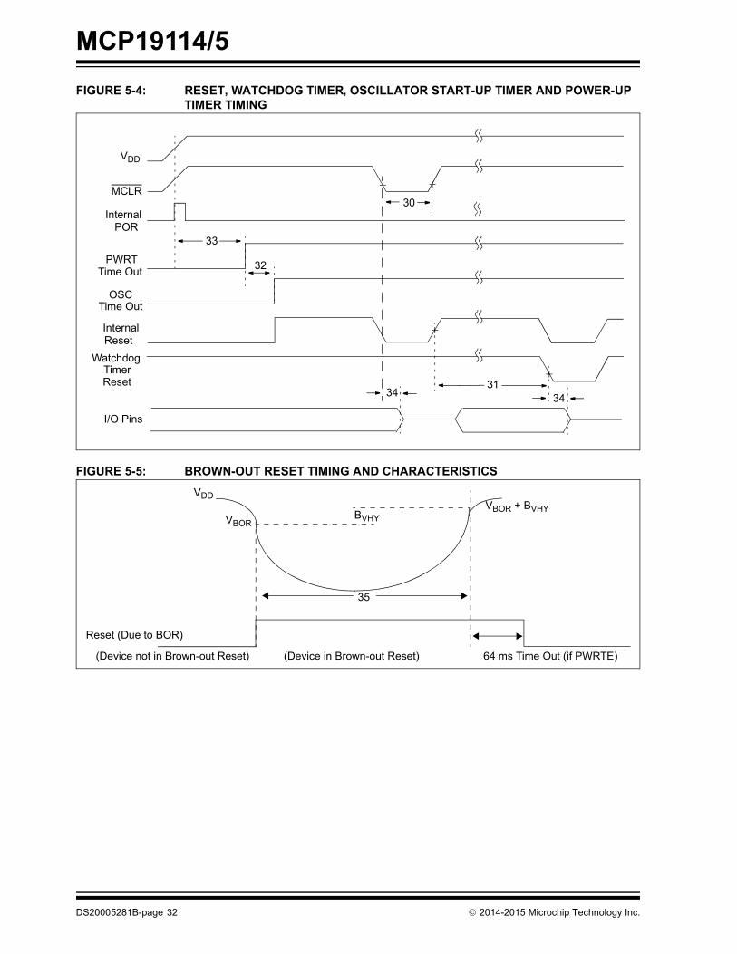
FIGURE 5-4: RESET, WATCHDOG TIMER, OSCILLATOR START-UP TIMER AND POWER-UPTIMER TIMING
FIGURE 5-5: BROWN-OUT RESET TIMING AND CHARACTERISTICS
VDD
MCLR
InternalPOR
PWRTTime Out
OSCTime Out
InternalReset
WatchdogTimerReset
33
32
30
3134
I/O Pins
34
VDD
VBORBVHY
VBOR + BVHY
Reset (Due to BOR)
(Device not in Brown-out Reset) (Device in Brown-out Reset) 64 ms Time Out (if PWRTE)
35
DS20005281B-page 32 2014-2015 Microchip Technology Inc.

MCP19114/5
FIGURE 5-6: TIMER0 AND TIMER1 EXTERNAL CLOCK TIMING
TABLE 5-3: RESET, WATCHDOG TIMER, OSCILLATOR START-UP TIMER AND POWER-UP TIMER REQUIREMENTS
Param. No. Sym. Characteristic Min. Typ.† Max. Units Conditions
30 TMCL MCLR Pulse Width (low) 2 — — s VDD = 5 V, -40°C to +85°C
31 TWDT Watchdog Timer Time-Out Period (No Prescaler)
7 18 33 ms VDD = 5 V, -40°C to +85°C
32 TOST Oscillation Start-Up Timer Period
— 1024TOSC — — TOSC = OSC1 period
33* TPWRT Power-up Timer Period (4 x TWDT)
28 72 132 ms VDD = 5 V, -40°C to +85°C
34 TIOZ I/O high impedance from MCLR Low or Watchdog Timer Reset
— — 2.0 µs
VBOR Brown-out Reset voltage 2.0 2.13 2.3 V
BVHY Brown-out Hysteresis — 100 — mV
35 TBCR Brown-out Reset pulse width 100* — — µs VDD VBOR (D005)
48 TCKEZ-TMR Delay from clock edge to timer increment
2TOSC — 7TOSC
* These parameters are characterized but not tested.† Data in “Typ.” column is at VIN = 12V (VDD = AVDD = 5V), 25°C unless otherwise stated. These parameters
are for design guidance only and are not tested.
41
42
40
T0CKI
TMR048
2014-2015 Microchip Technology Inc.
DS20005281B-page 33
MCP19114/5
FIGURE 5-7: PWM TIMINGS
TABLE 5-4: TIMER0 EXTERNAL CLOCK REQUIREMENTSParam.
No. Sym. Characteristic Min. Typ.† Max. Units Conditions
40* Tt0H T0CKI High Pulse Width No Prescaler 0.5TCY + 20 — — nsWith
Prescaler10 — — ns
41* Tt0L T0CKI Low Pulse Width No Prescaler 0.5TCY + 20 — — nsWith
Prescaler10 — — ns
42* Tt0P T0CKI Period Greater of:20 or
— — ns N = prescale value
(2, 4, ..., 256)
* These parameters are characterized but not tested.† Data in “Typ.” column is at VIN = 12V, 25°C unless otherwise stated. These parameters are for design guidance only
and are not tested.
TABLE 5-5: PWM REQUIREMENTSParam.
No. Sym. Characteristic Min. Typ.† Max. Units Conditions
53* TccR PWM (CLKPIN) output rise time — 10 25 ns
54* TccF PWM (CLKPIN) output fall time — 10 25 ns
* These parameters are characterized but not tested.† Data in “Typ” column is at VIN = 12V (AVDD = 4V), 25°C unless otherwise stated. Parameters are for
design guidance only and are not tested.
TCY 40+N-----------------------
Note: Refer to Figure 5-1 for load conditions.
53 54
PWM (CLKPIN)
DS20005281B-page
34 2014-2015 Microchip Technology Inc.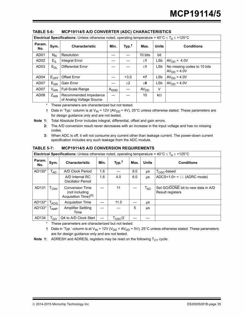
MCP19114/5
TABLE 5-6: MCP19114/5 A/D CONVERTER (ADC) CHARACTERISTICSElectrical Specifications: Unless otherwise noted, operating temperature = 40°C TA +125°C
Param. No. Sym. Characteristic Min. Typ.† Max. Units Conditions
AD01 NR Resolution — — 10 bits bitAD02 EIL Integral Error — — 1 LSb AVDD = 4.0V
AD03 EDL Differential Error — — 1 LSb No missing codes to 10 bitsAVDD = 4.0V
AD04 EOFF Offset Error — +3.0 +7 LSb AVDD = 4.0V
AD07 EGN Gain Error — 2 6 LSb AVDD = 4.0V
AD07 VAIN Full-Scale Range AGND — AVDD V
AD08 ZAIN Recommended Impedance of Analog Voltage Source
— — 10 k
* These parameters are characterized but not tested.† Data in ‘Typ.’ column is at VIN = 12V (AVDD = 4V), 25°C unless otherwise stated. These parameters are
for design guidance only and are not tested.Note 1: Total Absolute Error includes integral, differential, offset and gain errors.
2: The A/D conversion result never decreases with an increase in the input voltage and has no missing codes.
3: When ADC is off, it will not consume any current other than leakage current. The power-down current specification includes any such leakage from the ADC module.
TABLE 5-7: MCP19114/5 A/D CONVERSION REQUIREMENTSElectrical Specifications: Unless otherwise noted, operating temperature = 40°C TA +125°C
Param.No. Sym. Characteristic Min. Typ.† Max. Units Conditions
AD130* TAD A/D Clock Period 1.6 — 9.0 µs TOSC-basedA/D Internal RC Oscillator Period
1.6 4.0 6.0 µs ADCS<1:0> = 11 (ADRC mode)
AD131 TCNV Conversion Time(not including
Acquisition Time)(1)
— 11 — TAD Set GO/DONE bit to new data in A/D Result registers
AD132* TACQ Acquisition Time — 11.5 — µsAD133* TAMP Amplifier Settling
Time— — 5 µs
AD134 TGO Q4 to A/D Clock Start — TOSC/2 — —* These parameters are characterized but not tested.† Data in ‘Typ.’ column is at VIN = 12V (VDD = AVDD = 5V), 25°C unless otherwise stated. These parameters
are for design guidance only and are not tested.Note 1: ADRESH and ADRESL registers may be read on the following TCY cycle.
2014-2015 Microchip Technology Inc. DS20005281B-page 35

MCP19114/5
FIGURE 5-8: A/D CONVERSION TIMING131
130
132
BSF ADCON0, GO
Q4
A/D CLK
A/D DATA
ADRES
ADIF
GO
SAMPLE
OLD_DATA
SAMPLING STOPPED
NEW_DATA
9 8 7 3 2 1 0
1/2 TCY
6
134
DONE
Note 1: If the A/D clock source is selected as RC, a time of TCY is added before the A/D clock starts. Thisallows the SLEEP instruction to be executed.
DS20005281B-page 36 2014-2015 M
icrochip Technology Inc.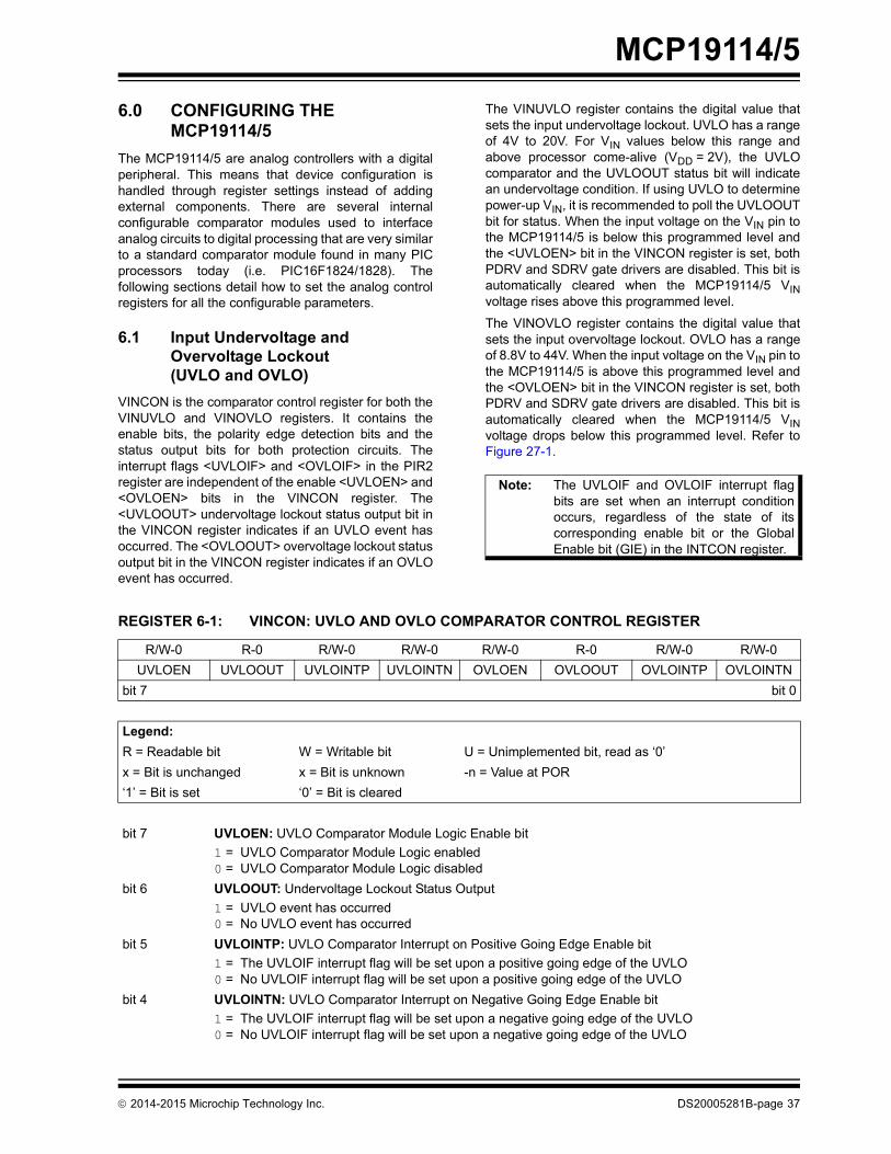
MCP19114/5
6.0 CONFIGURING THE MCP19114/5
The MCP19114/5 are analog controllers with a digitalperipheral. This means that device configuration ishandled through register settings instead of addingexternal components. There are several internalconfigurable comparator modules used to interfaceanalog circuits to digital processing that are very similarto a standard comparator module found in many PICprocessors today (i.e. PIC16F1824/1828). Thefollowing sections detail how to set the analog controlregisters for all the configurable parameters.
6.1 Input Undervoltage and Overvoltage Lockout(UVLO and OVLO)
VINCON is the comparator control register for both theVINUVLO and VINOVLO registers. It contains theenable bits, the polarity edge detection bits and thestatus output bits for both protection circuits. Theinterrupt flags <UVLOIF> and <OVLOIF> in the PIR2register are independent of the enable <UVLOEN> and<OVLOEN> bits in the VINCON register. The<UVLOOUT> undervoltage lockout status output bit inthe VINCON register indicates if an UVLO event hasoccurred. The <OVLOOUT> overvoltage lockout statusoutput bit in the VINCON register indicates if an OVLOevent has occurred.
2014-2015 Microchip Technology Inc.
The VINUVLO register contains the digital value thatsets the input undervoltage lockout. UVLO has a rangeof 4V to 20V. For VIN values below this range andabove processor come-alive (VDD = 2V), the UVLOcomparator and the UVLOOUT status bit will indicatean undervoltage condition. If using UVLO to determinepower-up VIN, it is recommended to poll the UVLOOUTbit for status. When the input voltage on the VIN pin tothe MCP19114/5 is below this programmed level andthe <UVLOEN> bit in the VINCON register is set, bothPDRV and SDRV gate drivers are disabled. This bit isautomatically cleared when the MCP19114/5 VINvoltage rises above this programmed level.
The VINOVLO register contains the digital value thatsets the input overvoltage lockout. OVLO has a rangeof 8.8V to 44V. When the input voltage on the VIN pin tothe MCP19114/5 is above this programmed level andthe <OVLOEN> bit in the VINCON register is set, bothPDRV and SDRV gate drivers are disabled. This bit isautomatically cleared when the MCP19114/5 VINvoltage drops below this programmed level. Refer toFigure 27-1.
Note: The UVLOIF and OVLOIF interrupt flagbits are set when an interrupt conditionoccurs, regardless of the state of itscorresponding enable bit or the GlobalEnable bit (GIE) in the INTCON register.
REGISTER 6-1: VINCON: UVLO AND OVLO COMPARATOR CONTROL REGISTER
R/W-0 R-0 R/W-0 R/W-0 R/W-0 R-0 R/W-0 R/W-0UVLOEN UVLOOUT UVLOINTP UVLOINTN OVLOEN OVLOOUT OVLOINTP OVLOINTN
bit 7 bit 0
Legend:R = Readable bit W = Writable bit U = Unimplemented bit, read as ‘0’x = Bit is unchanged x = Bit is unknown -n = Value at POR‘1’ = Bit is set ‘0’ = Bit is cleared
bit 7 UVLOEN: UVLO Comparator Module Logic Enable bit1 = UVLO Comparator Module Logic enabled0 = UVLO Comparator Module Logic disabled
bit 6 UVLOOUT: Undervoltage Lockout Status Output1 = UVLO event has occurred0 = No UVLO event has occurred
bit 5 UVLOINTP: UVLO Comparator Interrupt on Positive Going Edge Enable bit1 = The UVLOIF interrupt flag will be set upon a positive going edge of the UVLO0 = No UVLOIF interrupt flag will be set upon a positive going edge of the UVLO
bit 4 UVLOINTN: UVLO Comparator Interrupt on Negative Going Edge Enable bit1 = The UVLOIF interrupt flag will be set upon a negative going edge of the UVLO0 = No UVLOIF interrupt flag will be set upon a negative going edge of the UVLO
DS20005281B-page 37

MCP19114/5
bit 3 OVLOEN: OVLO Comparator Module Logic enable bit1 = OVLO Comparator Module Logic enabled0 = OVLO Comparator Module Logic disabled
bit 2 OVLOOUT: Overvoltage Lockout Status Output bit1 = OVLO event has occurred0 = No OVLO event has occurred
bit 1 OVLOINTP: OVLO Comparator Interrupt on Positive Going Edge Enable bit1 = The OVLOIF interrupt flag will be set upon a positive going edge of the OVLO0 = No OVLOIF interrupt flag will be set upon a positive going edge of the OVLO
bit 0 OVLOINTN: OVLO Comparator Interrupt on Negative Going Edge Enable bit1 = The OVLOIF interrupt flag will be set upon a negative going edge of the OVLO0 = No OVLOIF interrupt flag will be set upon a negative going edge of the OVLO
REGISTER 6-2: VINUVLO: INPUT UNDERVOLTAGE LOCKOUT REGISTER
U-0 U-0 R/W-x R/W-x R/W-x R/W-x R/W-x R/W-x— — UVLO5 UVLO4 UVLO3 UVLO2 UVLO1 UVLO0
bit 7 bit 0
Legend:R = Readable bit W = Writable bit U = Unimplemented bit, read as ‘0’u = Bit is unchanged x = Bit is unknown -n = Value at POR‘1’ = Bit is set ‘0’ = Bit is cleared
bit 7-6 Unimplemented: Read as ‘0’bit 5-0 UVLO<5:0>: Undervoltage Lockout Configuration bits
UVLO(V) = 3.5472 * (1.0285N) where N = the decimal value written to the VINUVLO Register from 0to 63
REGISTER 6-3: VINOVLO: INPUT OVERVOLTAGE LOCKOUT REGISTER
U-0 U-0 R/W-x R/W-x R/W-x R/W-x R/W-x R/W-x— — OVLO5 OVLO4 OVLO3 OVLO2 OVLO1 OVLO0
bit 7 bit 0
Legend:R = Readable bit W = Writable bit U = Unimplemented bit, read as ‘0’u = Bit is unchanged x = Bit is unknown -n = Value at POR‘1’ = Bit is set ‘0’ = Bit is cleared
bit 7-6 Unimplemented: Read as ‘0’bit 5-0 OVLO<5:0>: Overvoltage Lockout Configuration bits
OVLO(V) = 7.4847 * (1.0286N) where N = the decimal value written to the VINOVLO Register from 0to 63
REGISTER 6-1: VINCON: UVLO AND OVLO COMPARATOR CONTROL REGISTER (CONTINUED)
DS20005281B-page 38 2014-2015 Microchip Technology Inc.
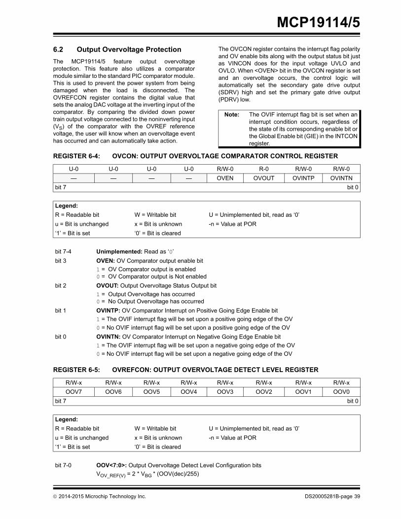
MCP19114/5
6.2 Output Overvoltage ProtectionThe MCP19114/5 feature output overvoltageprotection. This feature also utilizes a comparatormodule similar to the standard PIC comparator module.This is used to prevent the power system from beingdamaged when the load is disconnected. TheOVREFCON register contains the digital value thatsets the analog DAC voltage at the inverting input of thecomparator. By comparing the divided down powertrain output voltage connected to the noninverting input(VS) of the comparator with the OVREF referencevoltage, the user will know when an overvoltage eventhas occurred and can automatically take action.2014-2015 Microchip Technology Inc.
The OVCON register contains the interrupt flag polarityand OV enable bits along with the output status bit justas VINCON does for the input voltage UVLO andOVLO. When <OVEN> bit in the OVCON register is setand an overvoltage occurs, the control logic willautomatically set the secondary gate drive output(SDRV) high and set the primary gate drive output(PDRV) low.
Note: The OVIF interrupt flag bit is set when aninterrupt condition occurs, regardless ofthe state of its corresponding enable bit orthe Global Enable bit (GIE) in the INTCONregister.
REGISTER 6-4: OVCON: OUTPUT OVERVOLTAGE COMPARATOR CONTROL REGISTER
U-0 U-0 U-0 U-0 R/W-0 R-0 R/W-0 R/W-0— — — — OVEN OVOUT OVINTP OVINTN
bit 7 bit 0
Legend:R = Readable bit W = Writable bit U = Unimplemented bit, read as ‘0’u = Bit is unchanged x = Bit is unknown -n = Value at POR‘1’ = Bit is set ‘0’ = Bit is cleared
bit 7-4 Unimplemented: Read as ‘0’bit 3 OVEN: OV Comparator output enable bit
1 = OV Comparator output is enabled0 = OV Comparator output is Not enabled
bit 2 OVOUT: Output Overvoltage Status Output bit1 = Output Overvoltage has occurred0 = No Output Overvoltage has occurred
bit 1 OVINTP: OV Comparator Interrupt on Positive Going Edge Enable bit1 = The OVIF interrupt flag will be set upon a positive going edge of the OV0 = No OVIF interrupt flag will be set upon a positive going edge of the OV
bit 0 OVINTN: OV Comparator Interrupt on Negative Going Edge Enable bit1 = The OVIF interrupt flag will be set upon a negative going edge of the OV0 = No OVIF interrupt flag will be set upon a negative going edge of the OV
REGISTER 6-5: OVREFCON: OUTPUT OVERVOLTAGE DETECT LEVEL REGISTER
R/W-x R/W-x R/W-x R/W-x R/W-x R/W-x R/W-x R/W-xOOV7 OOV6 OOV5 OOV4 OOV3 OOV2 OOV1 OOV0
bit 7 bit 0
Legend:R = Readable bit W = Writable bit U = Unimplemented bit, read as ‘0’u = Bit is unchanged x = Bit is unknown -n = Value at POR‘1’ = Bit is set ‘0’ = Bit is cleared
bit 7-0 OOV<7:0>: Output Overvoltage Detect Level Configuration bitsVOV_REF(V) = 2 * VBG * (OOV(dec)/255)
DS20005281B-page 39

MCP19114/5
The A/D converter Calibration Word 8 can be used toimprove OVREF accuracy. An ADC measurementtarget (target in Example 6-1) is obtained by adding theanalog MUX buffer offset (BUOFFSET) to the desiredOVREF voltage (OVREFTARGET) and multiplying theresult by the ADC gain (GADC). OVREF is adjusteduntil the ADC reading equals or exceeds the target.An example of OVREF-calibration firmware is asfollows:
DS20005281B-page 40
\
EXAMPLE 6-1: EXAMPLE OVREF CORRECTION ROUTINE //Assumes that calibration words ADCCAL and BUFF are read from
//program memory into variables ADCC and BUOFFSET, respectively.
extern volatile unsigned int ADRES @ 0x01C;
#define OVREFTARGET (unsigned int) 0x0800 // OVREF Target = 2.0 V
unsigned long tmp = (unsigned long)ADCC*(OVREFTARGET+BUOFFSET); // ADC Reference + Buffer Offset
unsigned int target = (unsigned int)(tmp >> 15) - 3; // Subtract ADC typical offset error 3
unsigned int adc;
OVREFCON = 0x00; // Clear OVREFCON
ADCON0 = 0x09; // Enable and set channel to OVREF
do // Adjust OVREFCON
OVREFCON++;
NOP(); NOP();
adc = 0;
for (unsigned char i = 4; i > 0; i--)
ADCON0bits.GO_nDONE = 1;
while(ADCON0bits.GO_nDONE);
adc += ADRES;
adc >>= 2;
while ((adc < target) && (OVREFCON != 0xFF));
Note 1: In this example, the LSb weight of OVREFTARGET is set to 1/(210) volt. Users can choose their ownresolution depending on their accuracy requirement. The digital value of 2.0V is determined as follows:TRUNC(2.0 x 210) = 2048 (0x0800 hex).
2014-2015 Microchip Technology Inc.

MCP19114/5
6.3 Desaturation Detection forQuasi-Resonant OperationThe MCP19114/5 have been designed with a built-indesaturation detection comparator module custommade for quasi-resonant topologies. This is especiallyuseful for LED-type applications. Through the use ofthe MCP19114/5, both synchronous and asynchronousquasi-resonant topologies can be implemented. TheDESAT comparator module has the same features asthe UVLO/OVLO and OV comparator modules, exceptthat it includes some additional programmableparameters.
2014-2015 Microchip Technology Inc.
The DESATCON register holds the setup control bitsfor this module. Common control bits are the polarityedge trigger for the interrupt flag<CDSINTP><CDSINTN>, comparator output polaritycontrol <CDSPOL>, output enable <CDSOE> andoutput status <CDSOUT> bit. As with the othercomparator modules, the CDSIF is independent of theCDSOE enable bit. On the front end connected to theDESAT comparator noninverting input, there is atwo-channel MUX that connects either to the DESATPpin or to the fixed internally generated band gapvoltage. Additionally, the input offset voltage of theDESAT comparator is factory-trimmed to within ±1 mVtypically. These factory-trimmed values are stored inthe CALWD2 register at address 2081h. Firmwaremust read these values into the DSTCAL register(196h). If more offset is desired, the user can adjust thevalues written to the DSTCAL per their implementation.
REGISTER 6-6: DESATCON: DESATURATION COMPARATOR CONTROL REGISTER
R/W-0 R/W-0 R/W-0 R/W-0 R/W-0 R/W-0 R/W-0 R/W-0CDSMUX CDSWDE Reserved CDSPOL CDSOE CDSOUT CDSINTP CDSINTN
bit 7 bit 0
Legend:R = Readable bit W = Writable bit U = Unimplemented bit, read as ‘0’u = Bit is unchanged x = Bit is unknown -n = Value at POR‘1’ = Bit is set ‘0’ = Bit is cleared
bit 7 CDSMUX: DESAT Comparator Module Multiplexer channel selection bit1 = BG Selected0 = DESATP Selected (Default)
bit 6 CDSWDE: DESAT Comparator Watch Dog Enable bit1 = Watch Dog signal enables PWM Reset0 = Watch Dog signal does Not allow PWM reset
bit 5 Reservedbit 4 CDSPOL: DESAT Comparator Polarity Select bit
1 = DESAT Comparator output is inverted0 = DESAT Comparator output is Not inverted
bit 3 CDSOE: DESAT Comparator output enable bit1 = DESAT Comparator output PWM is enabled0 = DESAT Comparator output PWM is Not enabled
bit 2 CDSOUT: DESAT Comparator Output Status bitIf CDSPOL = 1 (inverted polarity)1 = CDSVP < CDSVN (DESAT Detected)0 = CDSVP > CDSVN (DESAT Not Detected)If CDSPOL = 0 (noninverted polarity)1 = CDSVP > CDSVN (DESAT Not Detected)0 = CDSVP < CDSVN (DESAT Detected)
bit 1 CDSINTP: CDSIF Comparator Interrupt on Positive Going Edge Enable bit1 = The CDSIF interrupt flag will be set upon a positive going edge0 = No CDSIF interrupt flag will be set upon a positive going edge
bit 0 CDSINTN: CDSIF Comparator Interrupt on Negative Going Edge Enable bit1 = The CDSIF interrupt flag will be set upon a negative going edge0 = No CDSIF interrupt flag will be set upon a negative going edge
DS20005281B-page 41

MCP19114/5
6.4 Primary Input Current OffsetAdjustPrimary input current offset adjust provides the abilityto add offset to the primary input current signal, thussetting a peak primary current limit. This offset adjust iscontrolled using the four bits in the ICOACON register.
DS20005281B-page 42
REGISTER 6-7: ICOACON: INPUT CURRENT OFFSET ADJUST CONTROL REGISTER
U-0 U-0 U-0 U-0 R/W-x R/W-x R/W-x R/W-x— — — — ICOAC3 ICOAC2 ICOAC1 ICOAC0
bit 7 bit 0
Legend:R = Readable bit W = Writable bit U = Unimplemented bit, read as ‘0’u = Bit is unchanged x = Bit is unknown -n = Value at POR‘1’ = Bit is set ‘0’ = Bit is cleared
bit 7-4 Unimplemented: Read as ‘0’bit 3-0 ICOAC<3:0>: Input current offset adjustment Configuration bits
0000 = 0 mV0001 = 50 mV0010 = 100 mV0011 = 150 mV0100 = 200 mV0101 = 250 mV0110 = 300 mV0111 = 350 mV1000 = 400 mV1001 = 450 mV1010 = 500 mV1011 = 550 mV1100 = 600 mV1101 = 650 mV1110 = 700 mV1111 = 750 mV
2014-2015 Microchip Technology Inc.

MCP19114/5
6.5 Leading Edge BlankingThe adjustable Leading Edge Blanking (LEB) is used toblank primary current spikes resulting from primaryswitch turn-on. Implementing adjustable LEB allowsthe system to ignore turn-on noise to best suit theapplication without primary current sense distortionfrom RC filtering. There are four settings available forLEB, including zero. These settings are controlled viatwo bits in the ICLEBCON register.2014-2015 Microchip Technology Inc.
REGISTER 6-8: ICLEBCON: INPUT CURRENT LEADING EDGE BLANKING CONTROL REGISTER
U-0 U-0 U-0 U-0 U-0 U-0 R/W-x R/W-x— — — — — — ICLEBC1 ICLEBC0
bit 7 bit 0
Legend:R = Readable bit W = Writable bit U = Unimplemented bit, read as ‘0’u = Bit is unchanged x = Bit is unknown -n = Value at POR‘1’ = Bit is set ‘0’ = Bit is cleared
bit 7-2 Unimplemented: Read as ‘0’bit 1-0 ICLEBC<1:0>: Input current Leading Edge Blanking Configuration bits
00 = 0 ns01 = 50 ns10 = 100 ns11 = 200 ns
DS20005281B-page 43

MCP19114/5
6.6 Slope CompensationA negative voltage slope is added to the output of theerror amplifier. This is done to prevent subharmonicinstability when:1. the operating duty cycle is greater than 50%2. wide changes in the duty cycle occur
The amount of negative slope added to the erroramplifier output is controlled by slope compensationslew rate control bits.
The slope compensation is enabled by clearing theSLPBY bit in the SLPCRCON register.
DS20005281B-page 44
REGISTER 6-9: SLPCRCON: SLOPE COMPENSATION RAMP CONTROL REGISTER
U-0 R/W-0 R/W-x R/W-x R/W-x R/W-x R/W-x R/W-x— SLPBY SLPS5 SLPS4 SLPS3 SLPS2 SLPS1 SLPS0
bit 7 bit 0
Legend:R = Readable bit W = Writable bit U = Unimplemented bit, read as ‘0’u = Bit is unchanged x = Bit is unknown -n = Value at POR‘1’ = Bit is set ‘0’ = Bit is cleared
bit 7 Unimplemented: Read as ‘0’bit 6 SLPBY: Slope Compensation Bypass Control bit
1 = Slope compensation is Bypassed0 = Slope compensation is not Bypassed
bit 5-0 SLPS<5:0>: Slope Compensation Slew Rate Control bitsSLPS (mV/µs) = 4.1505 mV/µs * e0.0739*(dec)
2014-2015 Microchip Technology Inc.
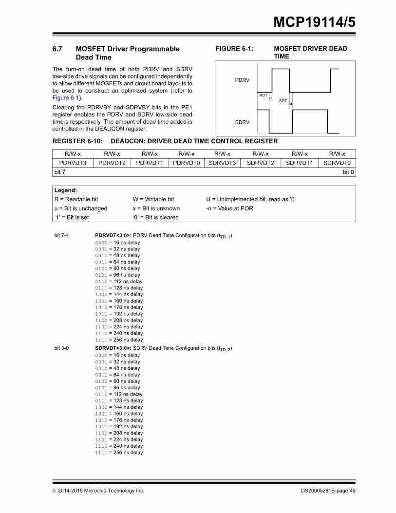
MCP19114/5
6.7 MOSFET Driver ProgrammableDead TimeThe turn-on dead time of both PDRV and SDRVlow-side drive signals can be configured independentlyto allow different MOSFETs and circuit board layouts tobe used to construct an optimized system (refer toFigure 6-1).
Clearing the PDRVBY and SDRVBY bits in the PE1register enables the PDRV and SDRV low-side deadtimers respectively. The amount of dead time added iscontrolled in the DEADCON register.
2014-2015 Microchip Technology Inc.
FIGURE 6-1: MOSFET DRIVER DEAD TIME
PDTSDT
PDRV
SDRV
REGISTER 6-10: DEADCON: DRIVER DEAD TIME CONTROL REGISTER
R/W-x R/W-x R/W-x R/W-x R/W-x R/W-x R/W-x R/W-xPDRVDT3 PDRVDT2 PDRVDT1 PDRVDT0 SDRVDT3 SDRVDT2 SDRVDT1 SDRVDT0
bit 7 bit 0
Legend:R = Readable bit W = Writable bit U = Unimplemented bit, read as ‘0’u = Bit is unchanged x = Bit is unknown -n = Value at POR‘1’ = Bit is set ‘0’ = Bit is cleared
bit 7-4 PDRVDT<3:0>: PDRV Dead Time Configuration bits (tTD_1)0000 = 16 ns delay0001 = 32 ns delay0010 = 48 ns delay0011 = 64 ns delay0100 = 80 ns delay0101 = 96 ns delay0110 = 112 ns delay0111 = 128 ns delay1000 = 144 ns delay1001 = 160 ns delay1010 = 176 ns delay1011 = 192 ns delay1100 = 208 ns delay1101 = 224 ns delay1110 = 240 ns delay1111 = 256 ns delay
bit 3-0 SDRVDT<3:0>: SDRV Dead Time Configuration bits (tTD_2)0000 = 16 ns delay0001 = 32 ns delay0010 = 48 ns delay0011 = 64 ns delay0100 = 80 ns delay0101 = 96 ns delay0110 = 112 ns delay0111 = 128 ns delay1000 = 144 ns delay1001 = 160 ns delay1010 = 176 ns delay1011 = 192 ns delay1100 = 208 ns delay1101 = 224 ns delay1110 = 240 ns delay1111 = 256 ns delay
DS20005281B-page 45

MCP19114/5
6.8 Output Regulation ReferenceVoltage ConfigurationThe VREFCON register controls the error amplifierreference voltage. This reference is used to set thecurrent or voltage regulation set point. VREFCONholds the digital value used by an 8-bit linear DACsetting the analog equivalent that gets summed withthe pedestal voltage (VZC) at the noninverting node ofthe error amplifier. VZC is equal to the band gapvoltage (1.23V). The output of the current senseamplifier A2 is also raised on the pedestal voltage,effectively canceling its effect on the input. Thepedestal is implemented throughout the analog controlloop to improve accuracy at low levels. The VREF DACcan be adjusted in 255 steps of 4.8 mV/step.
DS20005281B-page 46
REGISTER 6-11: VREFCON: CURRENT/VOLTAGE REGULATION SET POINT CONTROL REGISTER
R/W-0 R/W-0 R/W-0 R/W-0 R/W-0 R/W-0 R/W-0 R/W-0VREF7 VREF6 VREF5 VREF4 VREF3 VREF2 VREF1 VREF0
bit 7 bit 0
Legend:R = Readable bit W = Writable bit U = Unimplemented bit, read as ‘0’u = Bit is unchanged x = Bit is unknown -n = Value at POR‘1’ = Bit is set ‘0’ = Bit is cleared
bit 7-0 VREF<7:0>: Voltage-Controlling Current Regulation Set Point bitsVREF(V) = VBG * (VREF(dec)/255)
To ensure the best regulation accuracy whileimplementing the Current Sense Amplifier (A2), theinitial gain error must be considered. An 8-bitfactory-stored calibration value A2CAL<7:0> has beenstored in CALWD10 at 208Bh. This value can be usedto compensate for A2 gain error by adjusting the VREFcommand.
To get the final commanded value, the CALWD10 valuegets multiplied by the original VREF decimal commandusing the VREF expression, resulting in a 16-bit word.Rotating the 16 bit result right produces the finalcompensated command in the least significant byte.The most significant byte is unused.
An example of the firmware is as follows:
EXAMPLE 6-2: EXAMPLE A2 GAIN CORRECTION //Assumes that calibration word A2CAL has been read into variable A2COMP
unsigned int VREF1_TEMP = VREFCON*A2COMP; // A2 Gain compensate for VREFCON
VREF1_TEMP >>= 7;
VREF1_TEMP &= 0x00FF;
VREFCON = VREF1_TEMP;
2014-2015 Microchip Technology Inc.
MCP19114/5
6.9 VREF2 Voltage ReferenceThe VREF2CON register controls a second referenceDAC that can be used externally. For example, it can besent off chip and used to set the current regulation setpoint for a MCP1631 Pulse-Width Modulator. TheMCP19114/5 must be configured in Master Mode withbits MSC<0:1> = 01 in the MODECON register to2014-2015 Microchip Technology Inc.
connect VREF2 to GPB1. In Stand-Alone mode, VREF2is not accessible. VREFCON2 holds the digital valueused to set the VREF2 DAC. Since this reference isintended to go off chip, there is no pedestal offsetassociated with it and it is referenced to GND. It is an8-bit linear DAC and has a range from 0V to 1.23V (BG)equating to 255 steps at 4.8 mV/step.
REGISTER 6-12: VREF2CON: VREF2 VOLTAGE SET POINT REGISTER
R/W-0 R/W-0 R/W-0 R/W-0 R/W-0 R/W-0 R/W-0 R/W-0VREF27 VREF26 VREF25 VREF24 VREF23 VREF22 VREF21 VREF20
bit 7 bit 0
Legend:R = Readable bit W = Writable bit U = Unimplemented bit, read as ‘0’u = Bit is unchanged x = Bit is unknown -n = Value at POR‘1’ = Bit is set ‘0’ = Bit is cleared
bit 7-0 VREF2<7:0>: Voltage Controlling Current Regulation Set point bitsVREF2(V) = VBG * (VREF2(dec)/255)
The A/D converter Calibration Word 8 can be used toimprove VREF2 accuracy. An ADC measurement target(target in Example 6-3) is obtained by multiplying thedesired VREF2 voltage (VREF2TARGET) by the ADCgain (ADCC). VREF2 is adjusted until the ADC readingequals or exceeds the target.
An example of VREF2- correction firmware is as follows:
EXAMPLE 6-3: VREF2 CORRECTION ROUTINE// Assumes that the calibration word ADCCAL has been read into variable ADCC
extern volatile unsigned int ADRES @ 0x01C;
#define VREF2TARGET (unsigned int) 0x02CC // VREF2 Target = 0.7 V
unsigned long tmp = (unsigned long)ADCC*VREF2TARGET; // ADC Reference
unsigned int target = (unsigned int)(tmp >> 15) - 3; // Subtract ADC typical offset error 3
unsigned int adc;
VREF2CON = 0x00; // Clear VREF2CON
ADCON = 0x71; // Enable ADC and set channel to GPB1/VREF2
do // Adjust VREF2CON
VREF2CON++;
NOP(); NOP();
adc = 0;
for (unsigned char i = 4; i > 0; i--)
ADCON0bits.GO_nDONE = 1;
while(ADCON0bits.GO_nDONE);
adc += ADRES;
adc >>= 2;
while ((adc < target) && (VREF2CON != 0xFF));
Note 1: In this example, the LSb weight of VREF2TARGET is set to 1/(210) Volt. Users can choose their own resolution depending ontheir accuracy requirement. The digital value of 0.7V is determined as follows: TRUNC(0.7 x 210) = 716 (0x02CC hex).
(1)
DS20005281B-page 47
MCP19114/5
6.10 Analog Peripheral ControlThe MCP19114/5 have various analog peripherals.These peripherals can be configured to allowcustomizable operation. Refer to Register 6-13 formore information.6.10.1 MOSFET GATE DRIVER ENABLESThe MCP19114/5 can enable and/or disable theMOSFET gate driver outputs for the primary drive(PDRV) and the secondary drive (SDRV)independently. Setting the <PDRVEN> bit in the PE1register enables the primary drive. Setting the<SDRVEN> bit in the PE1 register enables thesecondary drive. Refer to Register 6-13 for details.
6.10.2 MOSFET DRIVER DEAD TIMEAs described in Section 6.7 “MOSFET DriverProgrammable Dead Time”, the MOSFET drive deadtime can be adjusted. The dead time can be setindependently for each driver from 16 ns to 256 ns inincrements of 16 ns using the DEADCON register.Dead time can also be disabled for each driverindependently by setting the bypass bits <PDRVBY>and <SDRVBY> in the PE1 register.
DS20005281B-page 48
6.10.3 SECONDARY CURRENT POSITIVE SENSE PULL-UP
A high-impedance pull-up on the ISP pin can beconfigured by setting the <ISPUEN> bit in the PE1register. When set, the ISP pin is internally pulled-up toVDD. Refer to Register 6-13 for details.
6.10.4 PWM STEERINGThe MCP19114/5 have additional control circuitry toallow open-loop repositioning of the output. ThePWMSTR_PEN bit enables a primary-only PWM signalof fixed frequency and duty cycle to reposition theoutput voltage up. The PWMSTR_SEN bit enables asecondary-only PWM signal of fixed frequency andduty cycle to reposition the output voltage down. Whenrepositioning output voltage down, the outputovervoltage protection must be active along withPWMSTR_SEN for the PWM to pulse the SDRV.Frequency and duty cycle are controlled through TMR2registers PR2 and TMR1L. PWMSTPR_PEN andPWMSTR_SEN should never be active at the sametime, therefore the PWMSTPR_PEN is the dominantbit. For quasi-resonant operation during open-looprepositioning, the DESAT comparator output should bedisabled with the <CDSOE> bit in the DEADCONregister.
REGISTER 6-13: PE1: ANALOG PERIPHERAL ENABLE1 CONTROL REGISTER
R/W-0 R/W-0 R/W-0 R/W-0 U-0 R/W-0 R/W-0 R/W-0PDRVEN SDRVEN PDRVBY SDRVBY — ISPUEN PWMSTR_PEN PWMSTR_SEN
bit 7 bit 0
Legend:R = Readable bit W = Writable bit U = Unimplemented bit, read as ‘0’u = Bit is unchanged x = Bit is unknown -n = Value at POR‘1’ = Bit is set ‘0’ = Bit is cleared
bit 7 PDRVEN: PDRV Gate Drive Enable bit1 = ENABLED0 = DISABLED
bit 6 SDRVEN: SDRV Gate Drive Enable bit1 = ENABLED0 = DISABLED
bit 5 PDRVBY: PDRV Dead Time Bypass bit1 = PDRV dead time is bypassed0 = PDRV dead time is not bypassed
bit 4 SDRVBY: SDRV Dead Time Bypass bit1 = SDRV dead time is bypassed0 = SDRV dead time is not bypassed.
bit 3 Unimplemented: Read as ‘0’bit 2 ISPUEN: ISP Weak Pull-Up Enable bit
1 = ISP weak pull-up is enabled0 = ISP weak pull-up is disabled
2014-2015 Microchip Technology Inc.

MCP19114/5
bit 1 PWMSTR_PEN: PDRV PWM Steering bit1 = Enables open-loop PWM control to the PDRV0 = Disables open-loop PWM control to the PDRV
bit 0 PWMSTR_SEN: SDRV PWM Steering bit1 = Enables open-loop PWM control to the SDRV0 = Disables open-loop PWM control to the SDRV
REGISTER 6-13: PE1: ANALOG PERIPHERAL ENABLE1 CONTROL REGISTER (CONTINUED)
6.11 Analog Blocks Enable ControlVarious analog circuit blocks can be enabled ordisabled, as shown in the ABECON register. TheABECON register also contains bits controlling analogand digital test signals. These signals can beconfigured to GPA0. Setting the <DIGOEN> bit enablesthe digital test signals to be connected to GPA0.<DSEL2:0> selects the digital channels. Setting<ANAOEN> enables the analog test signals to beconnected to GPA0. If <ANAOEN> and <DIGOEN>both get set, the DIGOEN bit takes priority. WhenANAOEN is not set, the analog test signals areconnected to the internal ADC. The analog test channelselections are controlled through the ADCON0 register.
6.11.1 MOSFET DRIVER UNDERVOLTAGE LOCKOUT SELECTION
The MOSFET gate drivers have internal undervoltageprotection that is controlled by the <DRUVSEL> bit inthe ABECON register. Since the gate drive supply isprovided externally through the VDR pin, the drivers arecapable of driving logic level FETs or higher 10V (13.5Vmaximum) FETs. <DRUVSEL> defaults to clear,therefore selecting a gate drive UVLO of 2.7V. Setting<DRUVSEL> selects the higher 5.4V gate drive UVLO.Refer to Section 4.2 “Electrical Characteristics” foradditional electrical specifications.
2014-2015 Microchip Technology Inc.
6.11.2 ERROR AMPLIFIER DISABLEThe error amplifier can be disabled such that its outputis parked to a known state. The <EADIS> bit defaults tozero and the error amp is enabled during normaloperation. In case the user wants to disable the erroramplifier, setting the EADIS bit parks the error amplifieroutput to just below the low clamp voltage. Undernormal operation, the error amplifier output runsbetween 2 * BG (upper clamp value) and 1 * BG –150 mV (lower clamp value). The analog feedback
circuitry utilizes an offset pedestal (1 * BG) to improveaccuracy at low levels.
REGISTER 6-14: ABECON: ANALOG BLOCK ENABLE CONTROL REGISTER
R/W-0 R/W-0 R/W-0 R/W-0 R/W-0 U-0 R/W-0 R/W-0DIGOEN DSEL2 DSEL1 DSEL0 DRUVSEL — EADIS ANAOEN
bit 7 bit 0
Legend:R = Readable bit W = Writable bit U = Unimplemented bit, read as ‘0’u = Bit is unchanged x = Bit is unknown -n = Value at POR‘1’ = Bit is set ‘0’ = Bit is cleared
bit 7 DIGOEN: DIG Test MUX to GPA0 connection control1 = DIG Test MUX output is connected to external pin GPA00 = DIG Test MUX output is not connected to external pin GPA0
DS20005281B-page 49
MCP19114/5
bit 6-4 DSEL<2:0> 000 = QRS (Output of DESAT comparator)001 = PWM_L (PWM output after monostable)010 = PWM (Oscillator output from the micro-controller)011 = TMR2EQ (When TMR2 equals PR2)100 = OV (Overvoltage comparator output)101 = SWFRQ (Switching Frequency Output)110 = SDRV_ON_ONESHOT (200 nS one-shot signal to reset WDM logic)111 = Unimplemented
bit 3 DRUVSEL: Selects gate drive undervoltage lockout level1 = Gate Drive UVLO set to 5.4V0 = Gate Drive UVLO set to 2.7V
bit 2 Unimplemented: Read as ‘0’bit 1 EADIS: Error Amplifier Disable bit
1 = Disables the error amplifier (Output parked low, clamped to 1 * BG)0 = Enables the error amplifier (Normal operation)
bit 0 ANAOEN: Analog MUX Output Control bit1 = Analog MUX output is connected to external pin GPA00 = Analog MUX output is not connected to external pin GPA0
REGISTER 6-14: ABECON: ANALOG BLOCK ENABLE CONTROL REGISTER (CONTINUED)
DS20005281B-page 50 2014-2015 Microchip Technology Inc.
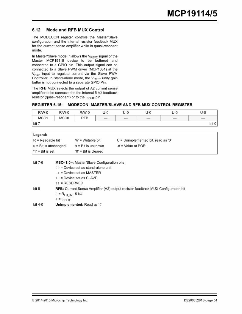
MCP19114/5
6.12 Mode and RFB MUX ControlThe MODECON register controls the Master/Slaveconfiguration and the internal resistor feedback MUXfor the current sense amplifier while in quasi-resonantmode.In Master/Slave mode, it allows the VREF2 signal of theMaster MCP19115 device to be buffered andconnected to a GPIO pin. This output signal can beconnected to a Slave PWM driver (MCP1631) at theVREF input to regulate current via the Slave PWMController. In Stand-Alone mode, the VREF2 unity gainbuffer is not connected to a separate GPIO Pin.
The RFB MUX selects the output of A2 current senseamplifier to be connected to the internal 5 k feedbackresistor (quasi-resonant) or to the ISOUT pin.
2014-2015 Microchip Technology Inc.
REGISTER 6-15: MODECON: MASTER/SLAVE AND RFB MUX CONTROL REGISTER
R/W-0 R/W-0 R/W-0 U-0 U-0 U-0 U-0 U-0MSC1 MSC0 RFB — — — — —
bit 7 bit 0
Legend:R = Readable bit W = Writable bit U = Unimplemented bit, read as ‘0’u = Bit is unchanged x = Bit is unknown -n = Value at POR‘1’ = Bit is set ‘0’ = Bit is cleared
bit 7-6 MSC<1:0>: Master/Slave Configuration bits00 = Device set as stand-alone unit01 = Device set as MASTER10 = Device set as SLAVE11 = RESERVED
bit 5 RFB: Current Sense Amplifier (A2) output resistor feedback MUX Configuration bit0 = RFB_INT 5 k1 = ISOUT
bit 4-0 Unimplemented: Read as ‘0’
DS20005281B-page 51

MCP19114/5
NOTES:DS20005281B-page 52
2014-2015 Microchip Technology Inc.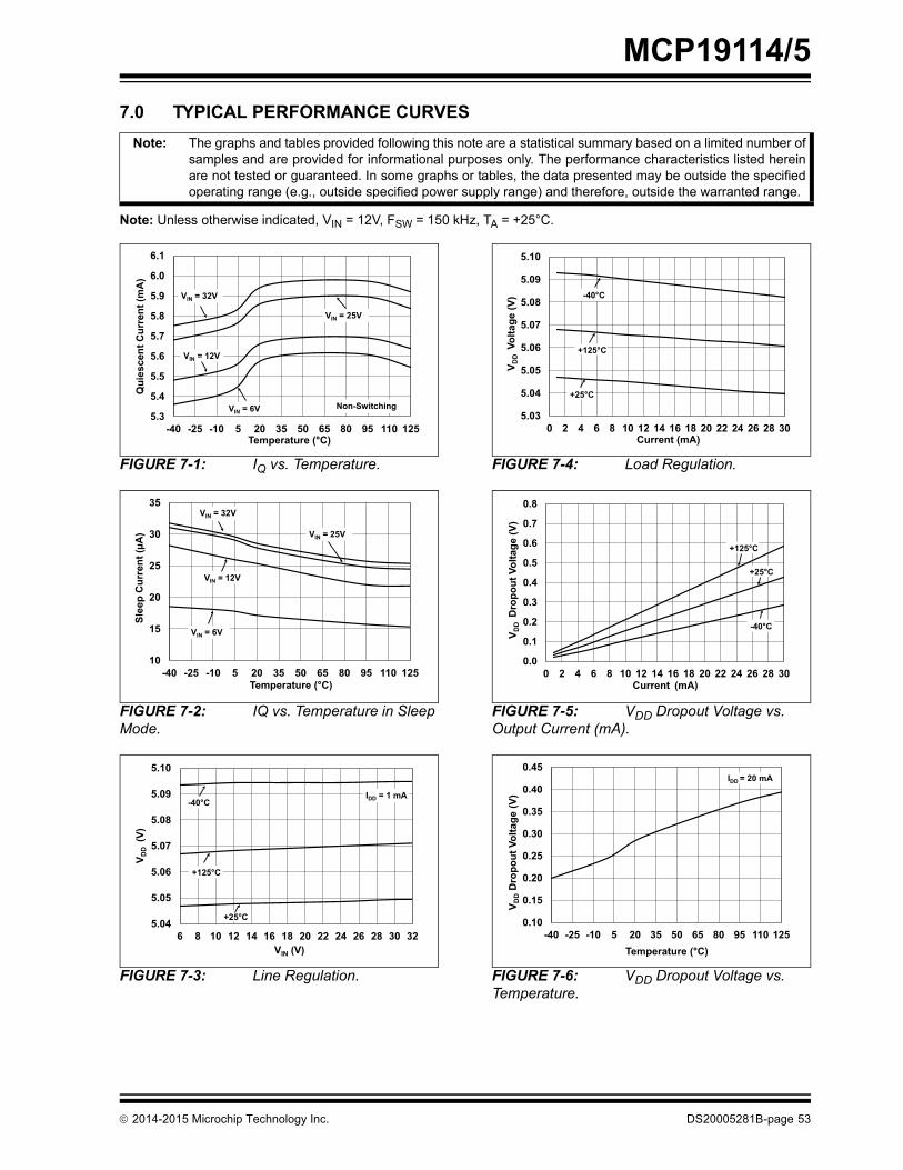
MCP19114/5
7.0 TYPICAL PERFORMANCE CURVES
Note: Unless otherwise indicated, VIN = 12V, FSW = 150 kHz, TA = +25°C.
Note: The graphs and tables provided following this note are a statistical summary based on a limited number ofsamples and are provided for informational purposes only. The performance characteristics listed hereinare not tested or guaranteed. In some graphs or tables, the data presented may be outside the specifiedoperating range (e.g., outside specified power supply range) and therefore, outside the warranted range.
FIGURE 7-1: IQ vs. Temperature.
FIGURE 7-2: IQ vs. Temperature in Sleep Mode.
FIGURE 7-3: Line Regulation.
5.3
5.4
5.5
5.6
5.7
5.8
5.9
6.0
6.1
-40 -25 -10 5 20 35 50 65 80 95 110 125
Qui
esce
nt C
urre
nt (m
A)
Temperature (°C)
VIN = 32V
VIN = 25V
VIN = 12V
VIN = 6V Non-Switching
10
15
20
25
30
35
-40 -25 -10 5 20 35 50 65 80 95 110 125
Slee
p C
urre
nt (μ
A)
Temperature (°C)
VIN = 32V
VIN = 25V
VIN = 12V
VIN = 6V
5.04
5.05
5.06
5.07
5.08
5.09
5.10
6 8 10 12 14 16 18 20 22 24 26 28 30 32
V DD
(V)
VIN (V)
-40°C
+125°C
+25°C
IDD = 1 mA
2014-2015 Microchip Technology Inc.
FIGURE 7-4: Load Regulation.
FIGURE 7-5: VDD Dropout Voltage vs. Output Current (mA).
FIGURE 7-6: VDD Dropout Voltage vs. Temperature.
5.03
5.04
5.05
5.06
5.07
5.08
5.09
5.10
0 2 4 6 8 10 12 14 16 18 20 22 24 26 28 30
V DD
Volta
ge (V
)
Current (mA)
-40°C
+25°C
+125°C
0.0
0.1
0.2
0.3
0.4
0.5
0.6
0.7
0.8
0 2 4 6 8 10 12 14 16 18 20 22 24 26 28 30
V DD
Dro
pout
Vol
tage
(V)
Current (mA)
-40°C
+25°C
+125°C
0.10
0.15
0.20
0.25
0.30
0.35
0.40
0.45
-40 -25 -10 5 20 35 50 65 80 95 110 125
V DD
Dro
pout
Vol
tage
(V)
Temperature (°C)
IDD = 20 mA
DS20005281B-page 53

MCP19114/5
Note: Unless otherwise indicated, VIN = 12V, FSW = 150 kHz, TA = +25°C.FIGURE 7-7: Output Driver Dead Time vs. Code and Temperature.
FIGURE 7-8: Sourcing Output Driver RDSon vs. Temperature.
FIGURE 7-9: Sinking Output Driver RDSon vs. Temperature.
0
50
100
150
200
250
300
0 2 4 6 8 10 12 14 16
PDR
V/SD
RV
Dea
d Ti
me
(ns)
Code (d)
-40°C
+25°C
+125°C
3.0
3.5
4.0
4.5
5.0
5.5
6.0
6.5
7.0
-40 -25 -10 5 20 35 50 65 80 95 110 125
RD
Son
()
Temperature (°C)
RPDRV-SOURCE
RSDRV-SOURCE
VDR = 10V
3.0
3.5
4.0
4.5
5.0
5.5
6.0
-40 -25 -10 5 20 35 50 65 80 95 110 125
RD
Son
()
Temperature (°C)
RPDRV-SINK
RSDRV-SINK
VDR = 10V
DS20005281B-page 54
FIGURE 7-10: Sourcing Output Driver RDSon vs. Temperature.
FIGURE 7-11: Sinking Output Driver RDSon vs. Temperature.
FIGURE 7-12: Oscillator Frequency vs. Temperature.
4.55.05.56.06.57.07.58.08.59.09.5
-40 -25 -10 5 20 35 50 65 80 95 110 125
RD
Son
()
Temperature (°C)
RPDRV-SOURCE
RSDRV-SOURCE
VDR = 5V
4.0
4.5
5.0
5.5
6.0
6.5
7.0
7.5
8.0
-40 -25 -10 5 20 35 50 65 80 95 110 125
RD
Son
()
Temperature (°C)
RPDRV-SINK
RSDRV-SINK
VDR = 5V
7.92
7.94
7.96
7.98
8.00
8.02
8.04
8.06
8.08
-40 -25 -10 5 20 35 50 65 80 95 110 125
Osc
illat
or F
requ
ency
(MH
z)
Temperature (°C)
2014-2015 Microchip Technology Inc.
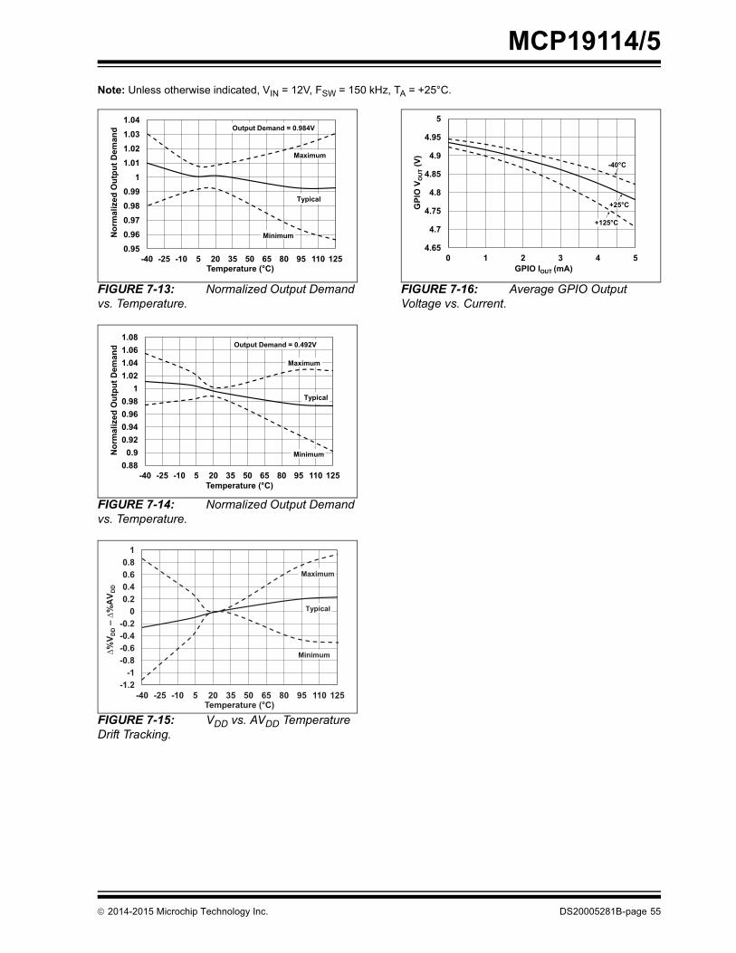
MCP19114/5
Note: Unless otherwise indicated, VIN = 12V, FSW = 150 kHz, TA = +25°C.FIGURE 7-13: Normalized Output Demand vs. Temperature.
FIGURE 7-14: Normalized Output Demand vs. Temperature.
FIGURE 7-15: VDD vs. AVDD Temperature Drift Tracking.
0.950.960.970.980.99
11.011.021.031.04
-40 -25 -10 5 20 35 50 65 80 95 110 125
Nor
mal
ized
Out
put D
eman
d
Temperature (°C)
Output Demand = 0.984V
Minimum
Maximum
Typical
0.880.9
0.920.940.960.98
11.021.041.061.08
-40 -25 -10 5 20 35 50 65 80 95 110 125
Nor
mal
ized
Out
put D
eman
d
Temperature (°C)
Output Demand = 0.492V
Minimum
Maximum
Typical
-1.2-1
-0.8-0.6-0.4-0.2
00.20.40.60.8
1
-40 -25 -10 5 20 35 50 65 80 95 110 125
%V D
D–
%A
V DD
Temperature (°C)
Minimum
Maximum
Typical
2014-2015 Microchip Technology Inc.
FIGURE 7-16: Average GPIO Output Voltage vs. Current.
4.65
4.7
4.75
4.8
4.85
4.9
4.95
5
0 1 2 3 4 5
GPI
O V
OU
T(V
)
GPIO IOUT (mA)
+125°C
-40°C
+25°C
DS20005281B-page 55

MCP19114/5
NOTES:DS20005281B-page 56
2014-2015 Microchip Technology Inc.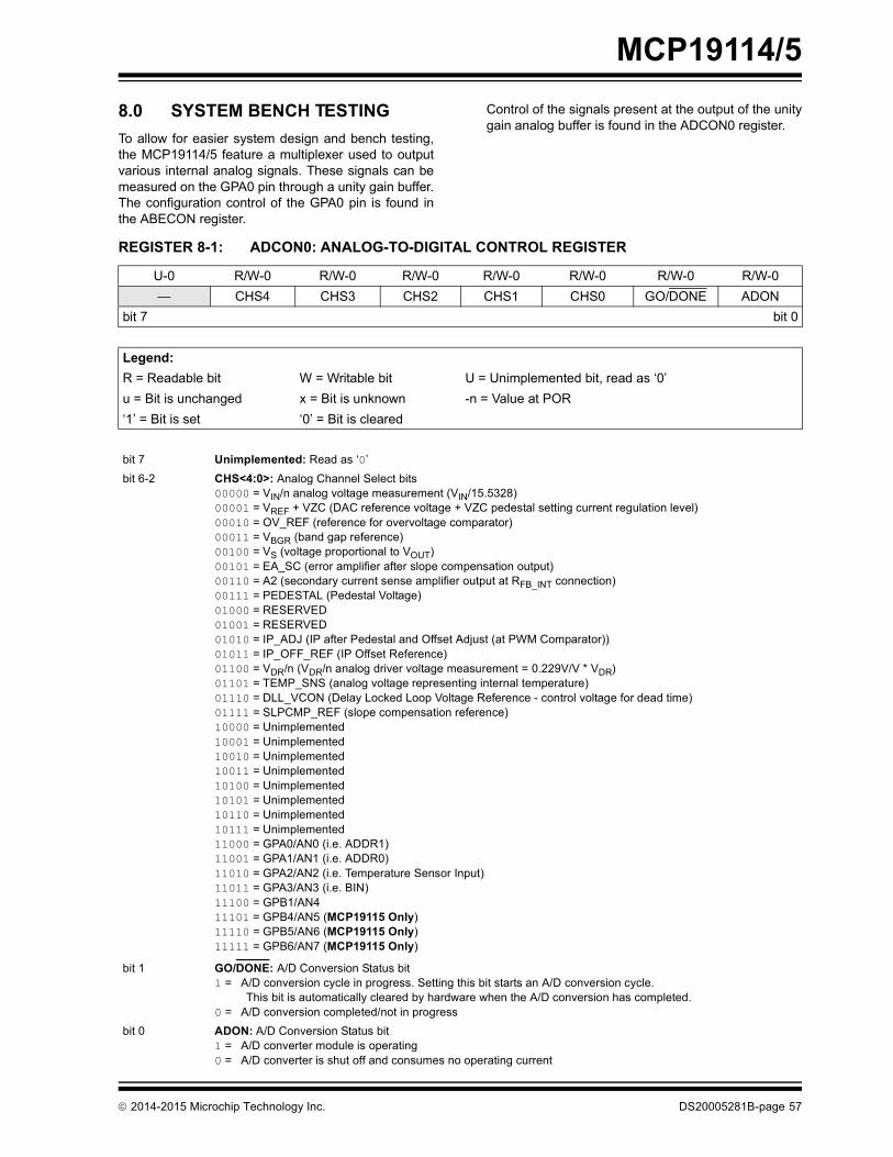
MCP19114/5
8.0 SYSTEM BENCH TESTINGTo allow for easier system design and bench testing,the MCP19114/5 feature a multiplexer used to outputvarious internal analog signals. These signals can bemeasured on the GPA0 pin through a unity gain buffer.The configuration control of the GPA0 pin is found inthe ABECON register..
2014-2015 Microchip Technology Inc.
Control of the signals present at the output of the unitygain analog buffer is found in the ADCON0 register.
REGISTER 8-1: ADCON0: ANALOG-TO-DIGITAL CONTROL REGISTER
U-0 R/W-0 R/W-0 R/W-0 R/W-0 R/W-0 R/W-0 R/W-0— CHS4 CHS3 CHS2 CHS1 CHS0 GO/DONE ADON
bit 7 bit 0
Legend:R = Readable bit W = Writable bit U = Unimplemented bit, read as ‘0’u = Bit is unchanged x = Bit is unknown -n = Value at POR ‘1’ = Bit is set ‘0’ = Bit is cleared
bit 7 Unimplemented: Read as ‘0’bit 6-2 CHS<4:0>: Analog Channel Select bits
00000 = VIN/n analog voltage measurement (VIN/15.5328)00001 = VREF + VZC (DAC reference voltage + VZC pedestal setting current regulation level)00010 = OV_REF (reference for overvoltage comparator)00011 = VBGR (band gap reference)00100 = VS (voltage proportional to VOUT)00101 = EA_SC (error amplifier after slope compensation output)00110 = A2 (secondary current sense amplifier output at RFB_INT connection)00111 = PEDESTAL (Pedestal Voltage)01000 = RESERVED01001 = RESERVED01010 = IP_ADJ (IP after Pedestal and Offset Adjust (at PWM Comparator))01011 = IP_OFF_REF (IP Offset Reference)01100 = VDR/n (VDR/n analog driver voltage measurement = 0.229V/V * VDR)01101 = TEMP_SNS (analog voltage representing internal temperature)01110 = DLL_VCON (Delay Locked Loop Voltage Reference - control voltage for dead time)01111 = SLPCMP_REF (slope compensation reference)10000 = Unimplemented10001 = Unimplemented10010 = Unimplemented10011 = Unimplemented10100 = Unimplemented10101 = Unimplemented10110 = Unimplemented10111 = Unimplemented11000 = GPA0/AN0 (i.e. ADDR1)11001 = GPA1/AN1 (i.e. ADDR0)11010 = GPA2/AN2 (i.e. Temperature Sensor Input)11011 = GPA3/AN3 (i.e. BIN)11100 = GPB1/AN411101 = GPB4/AN5 (MCP19115 Only)11110 = GPB5/AN6 (MCP19115 Only)11111 = GPB6/AN7 (MCP19115 Only)
bit 1 GO/DONE: A/D Conversion Status bit1 = A/D conversion cycle in progress. Setting this bit starts an A/D conversion cycle.
This bit is automatically cleared by hardware when the A/D conversion has completed.0 = A/D conversion completed/not in progress
bit 0 ADON: A/D Conversion Status bit1 = A/D converter module is operating0 = A/D converter is shut off and consumes no operating current
DS20005281B-page 57

MCP19114/5
NOTES:DS20005281B-page 58
2014-2015 Microchip Technology Inc.
MCP19114/5
9.0 DEVICE CALIBRATIONRead-only memory locations 2080h through 208Fhcontain factory calibration data. Refer to Section 17.0“Flash Program Memory Control” for information onhow to read from these memory locations.
9.1 Calibration Word 1Calibration Word 1 is at memory location 2080h. TheDCSRFB<6:0> bits set the offset calibration for thecurrent sense differential amplifier (A2) whenconfigured using the internal feedback resistor. Acalibration range of ±30 mV is provided with 20h and00h being midscale (no offset). The MSB is polarity only.Firmware must read these values and write them intothe DCSCAL register to implement offset calibration.
2014-2015 Microchip Technology Inc.
REGISTER 9-1: CALWD1: CALIBRATION WORD 1 REGISTER
U-0 U-0 U-0 U-0 U-0 U-0— — — — — —
bit 13 bit 8
U-0 R/P-1 R/P-1 R/P-1 R/P-1 R/P-1 R/P-1 R/P-1— DCSRFB6 DCSRFB5 DCSRFB4 DCSRFB3 DCSRFB2 DCSRFB1 DCSRFB0
bit 7 bit 0
Legend:R = Readable bit P = Programmable bit U = Unused bit, read as ‘0’-n = Value at POR ‘1’ = Bit is set ‘0’ = Bit is cleared x = Bit is unknown
bit 13-7 Unimplemented: Read as ‘0’bit 6-0 DCSRFB<6:0>: Input Differential Current Sense Calibration bits when configured using internal
feedback resistor
DS20005281B-page 59

MCP19114/5
9.2 Calibration Word 2Calibration Word 2 is at memory location 2081h. Itcontains the calibration bits for the desaturationcomparator current measurement input offset.Firmware must read these values and write them intothe DSTCAL register to implement the factory offsetcalibration. The factory offset calibration will minimizeoffset voltage. The desaturation comparator is one ofthe few examples where the user may want toimplement their own offset voltage values. Writing userdefined values to the DSTCAL register provides thisflexibility. This register also contains the trim bitsneeded to trim the internal 5k feedback resistor towithin 2% using the <RFBT5:0> bits. Firmware mustread these values and write them into the RFBTCALregister to implement the factory-trimmed feedbackresistor value.DS20005281B-page 60
REGISTER 9-2: CALWD2: CALIBRATION WORD 2 REGISTER
U-0 R/P-1 R/P-1 R/P-1 R/P-1 R/P-1— DST4 DST3 DST2 DST1 DST0
bit 13 bit 8
U-0 U-0 R/P-1 R/P-1 R/P-1 R/P-1 R/P-1 R/P-1— — RFBT5 RFBT4 RFBT3 RFBT2 RFBT1 RFBT0
bit 7 bit 0
Legend:R = Readable bit P = Programmable bit U = Unused bit, read as ‘0’-n = Value at POR ‘1’ = Bit is set ‘0’ = Bit is cleared x = Bit is unknown
bit 13 Unimplemented: Read as ‘0’bit 12-8 DST<4:0>: Desaturation Comparator Current Measure Offset calibration bits
11111 = Maximum negative offset calibration (-30 mV)••• 10000 = Mid scale (0 mV) 00000 = Mid scale (0 mV) •••01111 = Maximum positive offset calibration (+30 mV)
bit 7-6 Unimplemented: Read as ‘0’bit 5-0 RFBT<5:0>: Internal Feedback Resistor Trim bits
2014-2015 Microchip Technology Inc.

MCP19114/5
9.3 Calibration Word 3The VRO<5:0> bits at memory location 2082h calibratethe offset of the buffer amplifier of the output voltageregulation reference set point (VREF). Firmware mustread these values and write them to the VROCALregister for proper calibration.The BGR<3:0> bits at memory location 2082h calibratethe band gap reference. Firmware must read thesevalues and write them to the BGRCAL register forproper calibration.
2014-2015 Microchip Technology Inc.
REGISTER 9-3: CALWD3: CALIBRATION WORD 3 REGISTER
R/P-1 R/P-1 R/P-1 R/P-1 R/P-1 R/P-1VRO5 VRO4 VRO3 VRO2 VRO1 VRO0
bit 13 bit 8
U-0 U-0 U-0 U-0 R/P-1 R/P-1 R/P-1 R/P-1— — — — BGR3 BGR2 BGR1 BGR0
bit 7 bit 0
Legend:R = Readable bit P = Programmable bit U = Unused bit, read as ‘0’-n = Value at POR ‘1’ = Bit is set ‘0’ = Bit is cleared x = Bit is unknown
bit 13-8 VRO<5:0>: Reference voltage (VREF) offset calibration bitsbit 7-4 Unused: Read as ‘0’bit 3-0 BGR<3:0>: Band gap reference calibration bits
9.4 Calibration Word 4The TTA<3:0> bits at memory location 2083h containthe calibration bits for the factory-set overtemperaturethreshold. Firmware must read these values and writethem into the TTACAL register for proper calibration.
REGISTER 9-4: CALWD4: CALIBRATION WORD 4 REGISTER
U-0 U-0 U-0 U-0 U-0 U-0— — — — — —
bit 13 bit 8
U-0 U-0 U-0 U-0 R/P-1 R/P-1 R/P-1 R/P-1— — — — TTA3 TTA2 TTA1 TTA0
bit 7 bit 0
Legend:R = Readable bit P = Programmable bit U = Unused bit, read as ‘0’-n = Value at POR ‘1’ = Bit is set ‘0’ = Bit is cleared x = Bit is unknown
bit 13-4 Unimplemented: Read as ‘0’bit 3-0 TTA<3:0>: Overtemperature threshold calibration bits
DS20005281B-page 61
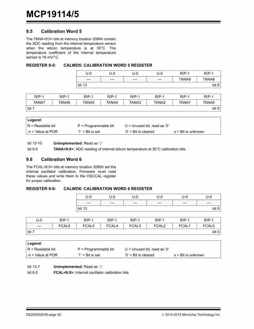
MCP19114/5
9.5 Calibration Word 5The TANA<9:0> bits at memory location 2084h containthe ADC reading from the internal temperature sensorwhen the silicon temperature is at 30°C. Thetemperature coefficient of the internal temperaturesensor is 16 mV/°C.DS20005281B-page 62
REGISTER 9-5: CALWD5: CALIBRATION WORD 5 REGISTER
U-0 U-0 U-0 U-0 R/P-1 R/P-1— — — — TANA9 TANA8
bit 13 bit 8
R/P-1 R/P-1 R/P-1 R/P-1 R/P-1 R/P-1 R/P-1 R/P-1TANA7 TANA6 TANA5 TANA4 TANA3 TANA2 TANA1 TANA0
bit 7 bit 0
Legend:R = Readable bit P = Programmable bit U = Unused bit, read as ‘0’-n = Value at POR ‘1’ = Bit is set ‘0’ = Bit is cleared x = Bit is unknown
bit 13-10 Unimplemented: Read as ‘0’bit 9-0 TANA<9:0>: ADC reading of internal silicon temperature at 30°C calibration bits
9.6 Calibration Word 6The FCAL<6:0> bits at memory location 2085h set theinternal oscillator calibration. Firmware must readthese values and write them to the OSCCAL registerfor proper calibration.
REGISTER 9-6: CALWD6: CALIBRATION WORD 6 REGISTER
U-0 U-0 U-0 U-0 U-0 U-0— — — — — —
bit 13 bit 8
U-0 R/P-1 R/P-1 R/P-1 R/P-1 R/P-1 R/P-1 R/P-1— FCAL6 FCAL5 FCAL4 FCAL3 FCAL2 FCAL1 FCAL0
bit 7 bit 0
Legend:R = Readable bit P = Programmable bit U = Unused bit, read as ‘0’-n = Value at POR ‘1’ = Bit is set ‘0’ = Bit is cleared x = Bit is unknown
bit 13-7 Unimplemented: Read as ‘0’bit 6-0 FCAL<6:0>: Internal oscillator calibration bits
2014-2015 Microchip Technology Inc.
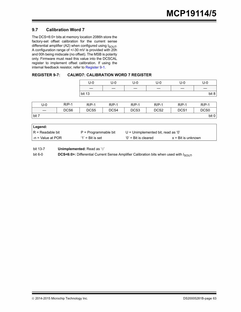
MCP19114/5
9.7 Calibration Word 7The DCS<6:0> bits at memory location 2086h store thefactory-set offset calibration for the current sensedifferential amplifier (A2) when configured using ISOUT.A configuration range of +/-30 mV is provided with 20hand 00h being midscale (no offset). The MSB is polarityonly. Firmware must read this value into the DCSCALregister to implement offset calibration. If using theinternal feedback resistor, refer to Register 9-1.2014-2015 Microchip Technology Inc.
REGISTER 9-7: CALWD7: CALIBRATION WORD 7 REGISTER
U-0 U-0 U-0 U-0 U-0 U-0— — — — — —
bit 13 bit 8
U-0 R/P-1 R/P-1 R/P-1 R/P-1 R/P-1 R/P-1 R/P-1— DCS6 DCS5 DCS4 DCS3 DCS2 DCS1 DCS0
bit 7 bit 0
Legend:R = Readable bit P = Programmable bit U = Unimplemented bit, read as ‘0’-n = Value at POR ‘1’ = Bit is set ‘0’ = Bit is cleared x = Bit is unknown
bit 13-7 Unimplemented: Read as ‘0’bit 6-0 DCS<6:0>: Differential Current Sense Amplifier Calibration bits when used with ISOUT.
DS20005281B-page 63
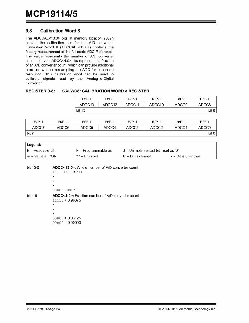
MCP19114/5
9.8 Calibration Word 8The ADCCAL<13:0> bits at memory location 2089hcontain the calibration bits for the A/D converter.Calibration Word 8 (ADCCAL <13:0>) contains thefactory measurement of the full scale ADC Reference.The value represents the number of A/D convertercounts per volt. ADCC<4:0> bits represent the fractionof an A/D converter count, which can provide additionalprecision when oversampling the ADC for enhancedresolution. This calibration word can be used tocalibrate signals read by the Analog-to-DigitalConverter.DS20005281B-page 64
REGISTER 9-8: CALWD8: CALIBRATION WORD 8 REGISTER
R/P-1 R/P-1 R/P-1 R/P-1 R/P-1 R/P-1ADCC13 ADCC12 ADCC11 ADCC10 ADCC9 ADCC8
bit 13 bit 8
R/P-1 R/P-1 R/P-1 R/P-1 R/P-1 R/P-1 R/P-1 R/P-1ADCC7 ADCC6 ADCC5 ADCC4 ADCC3 ADCC2 ADCC1 ADCC0
bit 7 bit 0
Legend:R = Readable bit P = Programmable bit U = Unimplemented bit, read as ‘0’-n = Value at POR ‘1’ = Bit is set ‘0’ = Bit is cleared x = Bit is unknown
bit 13-5 ADCC<13:5>: Whole number of A/D converter count111111111 = 511•••000000000 = 0
bit 4-0 ADCC<4:0>: Fraction number of A/D converter count11111 = 0.96875•••00001 = 0.0312500000 = 0.00000
2014-2015 Microchip Technology Inc.

MCP19114/5
9.9 Calibration Word 9Calibration Word 9 is at memory location 208Ah. Thevalue stored at this memory location represents theoffset voltage (in units of mV) of the analog test buffer.This is an 8-bit, two's complement word that can beused to compensate any signal sent through the Analogtest multiplexer. See section 8.0 for test signal details.2014-2015 Microchip Technology Inc.
REGISTER 9-9: CALWD9: CALIBRATION WORD 9 REGISTER
U-0 U-0 U-0 U-0 U-0 U-0— — — — — —
bit 13 bit 8
R/P-1 R/P-1 R/P-1 R/P-1 R/P-1 R/P-1 R/P-1 R/P-1BUFF7 BUFF6 BUFF5 BUFF4 BUFF3 BUFF2 BUFF1 BUFF0
bit 7 bit 0
Legend:R = Readable bit P = Programmable bit U = Unimplemented bit, read as ‘0’-n = Value at POR ‘1’ = Bit is set ‘0’ = Bit is cleared x = Bit is unknown
bit 13-8 Unimplemented: Read as ‘0’bit 7-0 BUFF<7:0>: Analog Buffer Offset calibration bits
11111111 = Mid-scale (-1 mV)•••10000000 = Largest negative offset (-128 mV)01111111 = Largest positive offset (127 mV)•••00000000 = Mid-scale (0 mV)
DS20005281B-page 65

MCP19114/5
9.10 Calibration Word 10The A2CAL<7:0> bits at memory location 208Bhcontain the calibration bits for Current Sense Amplifier(A2) Gain Error. For best regulation accuracy using thisamplifier, firmware can read this value and use it toadjust the VREF command. Section 6.8 “OutputRegulation Reference Voltage Configuration” fordetails.DS20005281B-page 66
REGISTER 9-10: CALWD10: CALIBRATION WORD 10 REGISTER
U-0 U-0 U-0 U-0 U-0 U-0— — — — — —
bit 13 bit 8
R/P-1 R/P-1 R/P-1 R/P-1 R/P-1 R/P-1 R/P-1 R/P-1A2CAL7 A2CAL6 A2CAL5 A2CAL4 A2CAL3 A2CAL2 A2CAL1 A2CAL0
bit 7 bit 0
Legend:R = Readable bit P = Programmable bit U = Unimplemented bit, read as ‘0’-n = Value at POR ‘1’ = Bit is set ‘0’ = Bit is cleared x = Bit is unknown
bit 13-8 Unimplemented: Read as ‘0’bit 7-0 A2CAL<7:0>: Current Sense Amplifier (A2) Gain Error Calibration bits
2014-2015 Microchip Technology Inc.
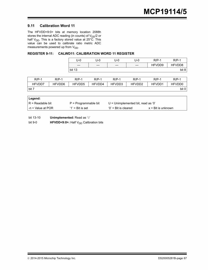
MCP19114/5
9.11 Calibration Word 11The HFVDD<9:0> bits at memory location 2088hstores the internal ADC reading (in counts) of VDD/2 orhalf VDD. This is a factory stored value at 25°C. Thisvalue can be used to calibrate ratio metric ADCmeasurements powered up from VDD.2014-2015 Microchip Technology Inc.
REGISTER 9-11: CALWD11: CALIBRATION WORD 11 REGISTER
U-0 U-0 U-0 U-0 R/P-1 R/P-1— — — — HFVDD9 HFVDD8
bit 13 bit 8
R/P-1 R/P-1 R/P-1 R/P-1 R/P-1 R/P-1 R/P-1 R/P-1HFVDD7 HFVDD6 HFVDD5 HFVDD4 HFVDD3 HFVDD2 HFVDD1 HFVDD0
bit 7 bit 0
Legend:R = Readable bit P = Programmable bit U = Unimplemented bit, read as ‘0’-n = Value at POR ‘1’ = Bit is set ‘0’ = Bit is cleared x = Bit is unknown
bit 13-10 Unimplemented: Read as ‘0’bit 9-0 HFVDD<9:0>: Half VDD Calibration bits
DS20005281B-page 67

MCP19114/5
NOTES:DS20005281B-page 68
2014-2015 Microchip Technology Inc.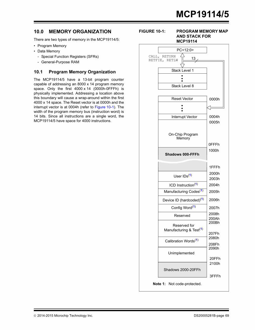
MCP19114/5
10.0 MEMORY ORGANIZATIONThere are two types of memory in the MCP19114/5:
• Program Memory• Data Memory
- Special Function Registers (SFRs)- General-Purpose RAM
10.1 Program Memory OrganizationThe MCP19114/5 have a 13-bit program countercapable of addressing an 8000 x 14 program memoryspace. Only the first 4000 x 14 (0000h-0FFFh) isphysically implemented. Addressing a location abovethis boundary will cause a wrap-around within the first4000 x 14 space. The Reset vector is at 0000h and theinterrupt vector is at 0004h (refer to Figure 10-1). Thewidth of the program memory bus (instruction word) is14 bits. Since all instructions are a single word, theMCP19114/5 have space for 4000 instructions.
2014-2015 Microchip Technology Inc.
FIGURE 10-1: PROGRAM MEMORY MAP AND STACK FOR MCP19114
PC<12:0>
13
0000h
0004h0005h
0FFFh
1FFFh
Stack Level 1
Stack Level 8
Reset Vector
Interrupt Vector
On-Chip ProgramMemory
CALL, RETURNRETFIE, RETLW
1000h
2000h
2005h
2006h
2007h
200Ah
207Fh
20FFh
2003h2004h
Note 1: Not code-protected.
Shadows 000-FFFh
2008h
2080h
200Bh
208Fh2090h
2100h
3FFFh
User IDs(1)
ICD Instruction(1)
Manufacturing Codes(1)
Device ID (hardcoded)(1)
Config Word(1)
Reserved
Reserved forManufacturing & Test(1)
Calibration Words(1)
Unimplemented
Shadows 2000-20FFh
DS20005281B-page 69
MCP19114/5
10.1.1 READING PROGRAM MEMORYAS DATAThere are two methods of accessing constants inprogram memory. The first method is to use tables ofRETLW instructions. The second method is to set aFiles Select Register (FSR) to point to the programmemory.
10.1.1.1 RETLW InstructionThe RETLW instruction can be used to provide accessto the tables of constants. The recommended way tocreate such tables is shown in Example 10-1.
EXAMPLE 10-1: RETLW INSTRUCTION
The BRW instruction makes this type of table verysimple to implement. If your code must remain portablewith previous generations of microcontrollers, then theBRW instruction is not available, so the older table-readmethod must be used.
constants
BRW ;Add Index in W to
;program counter to
;select data
RETLW DATA0 ;Index0 data
RETLW DATA1 ;Index1 data
RETLW DATA2
RETLW DATA3
my_function
;… LOTS OF CODE…
MOVLW DATA_INDEX
call constants
;… THE CONSTANT IS IN W
DS20005281B-page 70
10.2 Data Memory OrganizationThe data memory (refer to Figure 10-1) is partitionedinto four banks, which contain the General PurposeRegisters (GPR) and the Special Function Registers(SFR). The Special Function Registers are located inthe first 32 locations of each bank. Register locations20h-7Fh in Bank 0, A0h-EFh in Bank 1 and 120h-16Fhin Bank 2 are General Purpose Registers,implemented as static RAM. All other RAM isunimplemented and returns ‘0’ when read. TheRP<1:0> bits in the STATUS register are the bankselect bits.
EXAMPLE 10-2: BANK SELECT
To move values from one register to another register,the value must pass through the W register. Thismeans that for all register-to-register moves, twoinstruction cycles are required.
The entire data memory can be accessed eitherdirectly or indirectly. Direct addressing may require theuse of the RP<1:0> bits. Indirect addressing requiresthe use of the FSR. Indirect addressing uses theIndirect Register Pointer (IRP) bit in the STATUSregister for access to the Bank0/Bank1 or theBank2/Bank3 areas of data memory.
10.2.1 GENERAL PURPOSE REGISTER FILE
The register file is organized as 64 x 8 in theMCP19114/5. Each register is accessed, either directlyor indirectly, through the FSR (refer to Section 10.5“Indirect Addressing, INDF and FSR Registers”).
RP1 RP00 0 -> Bank 0 is selected0 1 -> Bank 1 is selected1 0 -> Bank 2 is selected1 1 -> Bank 3 is selected
2014-2015 Microchip Technology Inc.
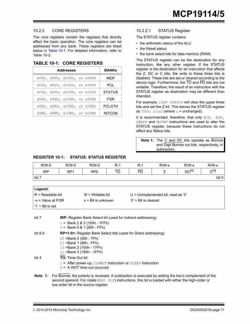
MCP19114/5
10.2.2 CORE REGISTERSThe core registers contain the registers that directlyaffect the basic operation. The core registers can beaddressed from any bank. These registers are listedbelow in Table 10-1. For detailed information, refer toTable 10-2.TABLE 10-1: CORE REGISTERSAddresses BANKx
x00h, x80h, x100h, or x180h INDF
x02h, x82h, x102h, or x182h PCL
x03h, x83h, x103h, or x183h STATUS
x04h, x84h, x104h, or x184h FSR
x0Ah, x8Ah, x10Ah, or x18Ah PCLATH
x0Bh, x8Bh, x10Bh, or x18Bh INTCON
2014-2015 Microchip Technology Inc.
10.2.2.1 STATUS RegisterThe STATUS register contains:
• the arithmetic status of the ALU• the Reset status• the bank select bits for data memory (RAM)
The STATUS register can be the destination for anyinstruction, like any other register. If the STATUSregister is the destination for an instruction that affectsthe Z, DC or C bits, the write to these three bits isdisabled. These bits are set or cleared according to thedevice logic. Furthermore, the TO and PD bits are notwritable. Therefore, the result of an instruction with theSTATUS register as destination may be different thanintended.
For example, CLRF STATUS will clear the upper threebits and set the Z bit. This leaves the STATUS registeras ‘000u u1uu’ (where u = unchanged).
It is recommended, therefore, that only BCF, BSF,SWAPF and MOVWF instructions are used to alter theSTATUS register, because these instructions do notaffect any Status bits.
Note 1: The C and DC bits operate as Borrowand Digit Borrow out bits, respectively, insubtraction.
REGISTER 10-1: STATUS: STATUS REGISTER
R/W-0 R/W-0 R/W-0 R-1 R-1 R/W-x R/W-x R/W-x
IRP RP1 RP0 TO PD Z DC(1) C(1)
bit 7 bit 0
Legend:R = Readable bit W = Writable bit U = Unimplemented bit, read as ‘0’-n = Value at POR x = Bit is unknown ‘0’ = Bit is cleared‘1’ = Bit is set
bit 7 IRP: Register Bank Select bit (used for Indirect addressing)1 = Bank 2 & 3 (100h - 1FFh)0 = Bank 0 & 1 (00h - FFh)
bit 6-5 RP<1:0>: Register Bank Select bits (used for Direct addressing)00 =Bank 0 (00h - 7Fh)01 =Bank 1 (80h - FFh)10 =Bank 2 (100h - 17Fh)11 =Bank 3 (180h - 1FFh)
bit 4 TO: Time-Out bit1 = After power-up, CLRWDT instruction or SLEEP instruction0 = A WDT time out occurred
Note 1: For Borrow, the polarity is reversed. A subtraction is executed by adding the two’s complement of the second operand. For rotate (RRF, RLF) instructions, this bit is loaded with either the high-order or low-order bit in the source register.
DS20005281B-page 71

MCP19114/5
bit 3 PD: Power-Down bit1 = After power-up or by the CLRWDT instruction0 = By execution of the SLEEP instruction
bit 2 Z: Zero bit1 = The result of an arithmetic or logic operation is zero0 = The result of an arithmetic or logic operation is not zero
bit 1 DC: Digit Carry/Digit Borrow bit(1) (ADDWF, ADDLW, SUBLW, SUBWF instructions)1 = A carry-out from the 4th low-order bit of the result occurred0 = No carry-out from the 4th low-order bit of the result
bit 0 C: Carry/Borrow bit(1) (ADDWF, ADDLW, SUBLW, SUBWF instructions)(1)
1 = A carry-out from the Most Significant bit of the result occurred0 = No carry-out from the Most Significant bit of the result occurred
REGISTER 10-1: STATUS: STATUS REGISTER (CONTINUED)
Note 1: For Borrow, the polarity is reversed. A subtraction is executed by adding the two’s complement of the second operand. For rotate (RRF, RLF) instructions, this bit is loaded with either the high-order or low-order bit in the source register.
10.2.3 SPECIAL FUNCTION REGISTERSThe Special Function Registers are registers used bythe CPU and peripheral functions for controlling thedesired operation of the device (refer to Figure 10-2).These registers are static RAM.
The special registers can be classified into two sets:core and peripheral. The Special Function Registersassociated with the microcontroller core are describedin this section. Those related to the operation of theperipheral features are described in the associatedsection for that peripheral feature.
DS20005281B-page 72
2014-2015 Microchip Technology Inc.
MCP19114/5
10.3 DATA MEMORY2014-2015 Microchip Technology Inc.
FIGURE 10-2: MCP19114/5 DATA MEMORY MAP
Indirect addr.(1) 00h Indirect addr. (1) 80h Indirect addr.(1) 100h Indirect addr. (1) 180hTMR0 01h OPTION_REG 81h TMR0 101h OPTION_REG 181hPCL 02h PCL 82h PCL 102h PCL 182h
STATUS 03h STATUS 83h STATUS 103h STATUS 183hFSR 04h FSR 84h FSR 104h FSR 184h
PORTGPA 05h TRISGPA 85h WPUGPA 105h IOCA 185hPORTGPB 06h TRISGPB 86h WPUGPB 106h IOCB 186h
PIR1 07h PIE1 87h PE1 107h ANSELA 187hPIR2 08h PIE2 88h MODECON 108h ANSELB 188h
PCON 09h 89h ABECON 109h 189hPCLATH 0Ah PCLATH 8Ah PCLATH 10Ah PCLATH 18AhINTCON 0Bh INTCON 8Bh INTCON 10Bh INTCON 18BhTMR1L 0Ch 8Ch 10Ch PORTICD(2) 18ChTMR1H 0Dh 8Dh 10Dh TRISICD(2) 18DhT1CON 0Eh 8Eh 10Eh ICKBUG(2) 18EhTMR2 0Fh 8Fh 10Fh BIGBUG(2) 18Fh
T2CON 10h VINUVLO 90h SSPADD 110h PMCON1 190hPR2 11h VINOVLO 91h SSPBUF 111h PMCON2 191h
12h VINCON 92h SSPCON1 112h PMADRL 192hPWMPHL 13h CC1RL 93h SSPCON2 113h PMADRH 193hPWMPHH 14h CC1RH 94h SSPCON3 114h PMDATL 194hPWMRL 15h CC2RL 95h SSPMSK1 115h PMDATH 195hPWMRH 16h CC2RH 96h SSPSTAT 116h DSTCAL 196h
17h CCDCON 97h SSPADD2 117h RFBTCAL 197h18h DESATCON 98h SSPMSK2 118h OSCCAL 198h
VREFCON 19h OVCON 99h 119h DCSCAL 199hVREF2CON 1Ah OVREFCON 9Ah 11Ah TTACAL 19AhOSCTUNE 1Bh DEADCON 9Bh 11Bh BGRCAL 19BhADRESL 1Ch SLPCRCON 9Ch 11Ch VROCAL 19ChADRESH 1Dh ICOACON 9Dh 11Dh 19DhADCON0 1Eh ICLEBCON 9Eh 11Eh 19EhADCON1 1Fh 9Fh 11Fh Reserved 19Fh
General Purpose Register
96 Bytes
20h GeneralPurposeRegister80 Bytes
A0h GeneralPurposeRegister
80 bytes
120h 1A0h
EFh 16F 1EF
7Fh
AccessesBank 0
F0h
FFh
AccessesBank 0
170h
17Fh
AccessesBank 0
1F0h
1FFh
Bank 0 Bank 1 Bank2 Bank3
Unimplemented data memory locations, read as '0'.Note 1: Not a physical register.
2: Only accessible when DBGEN = 0 and ICKBUG<INBUG> = 1.
FileAddress
FileAddress
FileAddress
FileAddress
DS20005281B-page 73

MC
P19114/5
DS
20005281B-page 74
2014-2015 M
icrochip Technology Inc.
alue on POR Reset Value on all other resets(1)
xxxx xxxx xxxx xxxx
xxxx xxxx uuuu uuuu
0000 0000 0000 0000
0001 1xxx 000q quuu
xxxx xxxx uuuu uuuu
xxx- xxxx uuu- uuuu
xxxx --xx uuuu --uu
-000 0000 -000 0000
0--0 0000 0--0 0000
---- --qq ---- --uu
---0 0000 ---0 0000
0000 000x 0000 000u
xxxx xxxx uuuu uuuu
xxxx xxxx uuuu uuuu
--00 --00 --uu --uu
0000 0000 uuuu uuuu
---- -000 ---- -000
1111 1111 1111 1111
— —
xxxx xxxx uuuu uuuu
xxxx xxxx uuuu uuuu
xxxx xxxx uuuu uuuu
xxxx xxxx uuuu uuuu
— —
— —
0000 0000 0000 0000
0000 0000 0000 0000
---0 0000 ---0 0000
xxxx xxxx uuuu uuuu
0000 00xx 0000 00uu
-000 0000 -000 0000
-000 ---- -000 ----
ed = unimplemented
t will be set again if the mismatch exists.
TABLE 10-2: MCP19114/5 SPECIAL REGISTERS SUMMARY BANK 0Adr Name Bit 7 Bit 6 Bit 5 Bit 4 Bit 3 Bit 2 Bit 1 Bit 0 V
Bank 0
00h INDF Addressing this location uses contents of FSR to address data memory (not a physical register)
01h TMR0 Timer0 Module’s Register
02h PCL Program Counter's (PC) Least Significant byte
03h STATUS IRP RP1 RP0 TO PD Z DC C
04h FSR Indirect data memory address pointer
05h PORTGPA GPA7 GPA6 GPA5 — GPA3 GPA2 GPA1 GPA0
06h PORTGPB GPB7 GPB6 GPB5 GPB4 — — GPB1 GPB0
07h PIR1 — ADIF BCLIF SSPIF CC2IF CC1IF TMR2IF TMR1IF
08h PIR2 CDSIF — — OTIF OVIF DRUVIF OVLOIF UVLOIF
09h PCON — — — — — — POR BOR
0Ah PCLATH — — — Write buffer for upper 5 bits of program counter
0Bh INTCON GIE PEIE T0IE INTE IOCE T0IF INTF IOCF(2)
0Ch TMR1L Holding register for the Least Significant byte of the 16-bit TMR1
0Dh TMR1H Holding register for the Most Significant byte of the 16-bit TMR1
0Eh T1CON — — T1CKPS1 T1CKPS0 — — TMR1CS TMR1ON
0Fh TMR2 Timer2 Module Register
10h T2CON — — — — — TMR2ON T2CKPS1 T2CKPS0
11h PR2 Timer2 Module Period Register
12h — Unimplemented
13h PWMPHL SLAVE Phase Shift Register
14h PWMPHH SLAVE Phase Shift Register
15h PWMRL PWM Register Low Byte
16h PWMRH PWM Register High Byte
17h — Unimplemented
18h — Unimplemented
19h VREFCON VREF7 VREF6 VREF5 VREF4 VREF3 VREF2 VREF1 VREF0
1Ah VREF2CON VREF27 VREF26 VREF25 VREF24 VREF23 VREF22 VREF21 VREF20
1Bh OSCTUNE — — — TUN4 TUN3 TUN2 TUN1 TUN0
1Ch ADRESL Least significant 8 bits of the A/D result
1Dh ADRESH Most significant 2 bits of the A/D result
1Eh ADCON0 — CHS4 CHS3 CHS2 CHS1 CHS0 GO/DONE ADON
1Fh ADCON1 — ADCS2 ADCS1 ADCS0 — — — —
Legend: — = Unimplemented locations read as ‘0’, u = unchanged, x = unknown, q = value depends on condition, shadNote 1: Other (non power-up) resets include MCLR Reset and Watchdog Timer Reset during normal operation.
2: MCLR and WDT reset does not affect the previous value data latch. The IOCF bit will be cleared upon reset bu
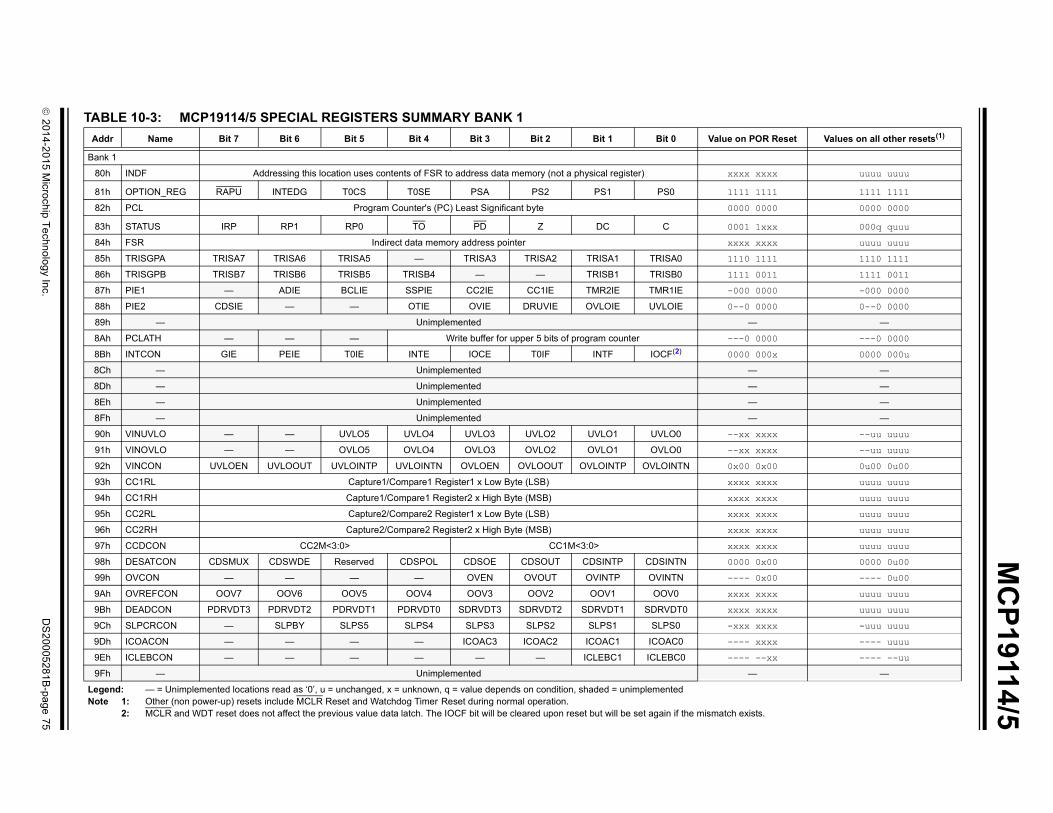
2014-2015 M
icrochip Technology Inc.D
S20005281B
-page 75
MC
P19114/5
TAA POR Reset Values on all other resets(1)
Ba
8 x xxxx uuuu uuuu
8 1 1111 1111 1111
8 0 0000 0000 0000
8 1 1xxx 000q quuu
8 x xxxx uuuu uuuu
8 0 1111 1110 1111
8 1 0011 1111 0011
8 0 0000 -000 0000
8 0 0000 0--0 0000
8 — —
8 0 0000 ---0 0000
8 0 000x 0000 000u
8 — —
8 — —
8 — —
8 — —
9 x xxxx --uu uuuu
9 x xxxx --uu uuuu
9 0 0x00 0u00 0u00
9 x xxxx uuuu uuuu
9 x xxxx uuuu uuuu
9 x xxxx uuuu uuuu
9 x xxxx uuuu uuuu
9 x xxxx uuuu uuuu
9 0 0x00 0000 0u00
9 - 0x00 ---- 0u00
9 x xxxx uuuu uuuu
9 x xxxx uuuu uuuu
9 x xxxx -uuu uuuu
9 - xxxx ---- uuuu
9 - --xx ---- --uu
9 — —
LeNo
xists.
BLE 10-3: MCP19114/5 SPECIAL REGISTERS SUMMARY BANK 1ddr Name Bit 7 Bit 6 Bit 5 Bit 4 Bit 3 Bit 2 Bit 1 Bit 0 Value on
nk 1
0h INDF Addressing this location uses contents of FSR to address data memory (not a physical register) xxx
1h OPTION_REG RAPU INTEDG T0CS T0SE PSA PS2 PS1 PS0 111
2h PCL Program Counter's (PC) Least Significant byte 000
3h STATUS IRP RP1 RP0 TO PD Z DC C 000
4h FSR Indirect data memory address pointer xxx
5h TRISGPA TRISA7 TRISA6 TRISA5 — TRISA3 TRISA2 TRISA1 TRISA0 111
6h TRISGPB TRISB7 TRISB6 TRISB5 TRISB4 — — TRISB1 TRISB0 111
7h PIE1 — ADIE BCLIE SSPIE CC2IE CC1IE TMR2IE TMR1IE -00
8h PIE2 CDSIE — — OTIE OVIE DRUVIE OVLOIE UVLOIE 0--
9h — Unimplemented
Ah PCLATH — — — Write buffer for upper 5 bits of program counter ---
Bh INTCON GIE PEIE T0IE INTE IOCE T0IF INTF IOCF(2) 000
Ch — Unimplemented
Dh — Unimplemented
Eh — Unimplemented
Fh — Unimplemented
0h VINUVLO — — UVLO5 UVLO4 UVLO3 UVLO2 UVLO1 UVLO0 --x
1h VINOVLO — — OVLO5 OVLO4 OVLO3 OVLO2 OVLO1 OVLO0 --x
2h VINCON UVLOEN UVLOOUT UVLOINTP UVLOINTN OVLOEN OVLOOUT OVLOINTP OVLOINTN 0x0
3h CC1RL Capture1/Compare1 Register1 x Low Byte (LSB) xxx
4h CC1RH Capture1/Compare1 Register2 x High Byte (MSB) xxx
5h CC2RL Capture2/Compare2 Register1 x Low Byte (LSB) xxx
6h CC2RH Capture2/Compare2 Register2 x High Byte (MSB) xxx
7h CCDCON CC2M<3:0> CC1M<3:0> xxx
8h DESATCON CDSMUX CDSWDE Reserved CDSPOL CDSOE CDSOUT CDSINTP CDSINTN 000
9h OVCON — — — — OVEN OVOUT OVINTP OVINTN ---
Ah OVREFCON OOV7 OOV6 OOV5 OOV4 OOV3 OOV2 OOV1 OOV0 xxx
Bh DEADCON PDRVDT3 PDRVDT2 PDRVDT1 PDRVDT0 SDRVDT3 SDRVDT2 SDRVDT1 SDRVDT0 xxx
Ch SLPCRCON — SLPBY SLPS5 SLPS4 SLPS3 SLPS2 SLPS1 SLPS0 -xx
Dh ICOACON — — — — ICOAC3 ICOAC2 ICOAC1 ICOAC0 ---
Eh ICLEBCON — — — — — — ICLEBC1 ICLEBC0 ---
Fh — Unimplemented
gend: — = Unimplemented locations read as ‘0’, u = unchanged, x = unknown, q = value depends on condition, shaded = unimplementedte 1: Other (non power-up) resets include MCLR Reset and Watchdog Timer Reset during normal operation.
2: MCLR and WDT reset does not affect the previous value data latch. The IOCF bit will be cleared upon reset but will be set again if the mismatch e
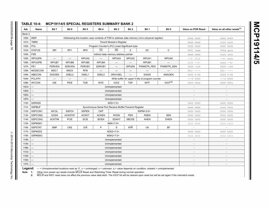
MC
P19114/5
DS
20005281B-page 76
2014-2015 M
icrochip Technology Inc.
alue on POR Reset Value on all other resets(1)
xxxx xxxx xxxx xxxx
xxxx xxxx uuuu uuuu
0000 0000 0000 0000
0001 1xxx 000q quuu
xxxx xxxx uuuu uuuu
--1- 1111 --u- uuuu
1111 --1- uuuu --u-
0000 -100 0000 -100
001- ---- 001- ----
0000 0-00 0000 0-00
---0 0000 ---0 0000
0000 000x 0000 000u
— —
— —
— —
— —
0000 0000 0000 0000
xxxx xxxx uuuu uuuu
0000 0000 0000 0000
0000 0000 0000 0000
0000 0000 0000 0000
1111 1111 1111 1111
— —
0000 0000 0000 0000
1111 1111 1111 1111
— —
— —
— —
— —
— —
— —
— —
atch exists.
TABLE 10-4: MCP19114/5 SPECIAL REGISTERS SUMMARY BANK 2Adr Name Bit 7 Bit 6 Bit 5 Bit 4 Bit 3 Bit 2 Bit 1 Bit 0 V
Bank 2
100h INDF Addressing this location uses contents of FSR to address data memory (not a physical register)
101h TMR0 Timer0 Module’s Register
102h PCL Program Counter's (PC) Least Significant byte
103h STATUS IRP RP1 RP0 TO PD Z DC C
104h FSR Indirect data memory address pointer
105h WPUGPA — — WPUA5 — WPUA3 WPUA2 WPUA1 WPUA0
106h WPUGPB WPUB7 WPUB6 WPUB5 WPUB4 — — WPUB1 —
107h PE1 PDRVEN SDRVEN PDRVBY SDRVBY — ISPUEN PWMSTR_PEN PWMSTR_SEN
108h MODECON MSC1 MSC0 RFB — — — — —
109h ABECON DIGOEN DSEL2 DSEL1 DSEL0 DRUVSEL — EADIS ANAOEN
10Ah PCLATH — — — Write buffer for upper 5 bits of program counter
10Bh INTCON GIE PEIE T0IE INTE IOCE T0IF INTF IOCF(2)
10Ch — Unimplemented
10Dh — Unimplemented
10Eh — Unimplemented
10Fh — Unimplemented
110h SSPADD ADD<7:0>
111h SSPBUF Synchronous Serial Port Receive Buffer/Transmit Register
112h SSPCON1 WCOL SSPOV SSPEN CKP SSPM<3:0>
113h SSPCON2 GCEN ACKSTAT ACKDT ACKEN RCEN PEN RSEN SEN
114h SSPCON3 ACKTIM PCIE SCIE BOEN SDAHT SBCDE AHEN DHEN
115h SSPMSK1 MSK<7:0>
116h SSPSTAT SMP CKE D/A P S R/W UA BF
117h SSPADD2 ADD2<7:0>
118h SSPMSK2 MSK2<7:0>
119h — Unimplemented
11Ah — Unimplemented
11Bh — Unimplemented
11Ch — Unimplemented
11Dh — Unimplemented
11Eh — Unimplemented
11Fh — Unimplemented
Legend: — = Unimplemented locations read as ‘0’, u = unchanged, x = unknown, q = value depends on condition, shaded = unimplementedNote 1: Other (non power-up) resets include MCLR Reset and Watchdog Timer Reset during normal operation.
2: MCLR and WDT reset does not affect the previous value data latch. The IOCF bit will be cleared upon reset but will be set again if the mism

2014-2015 M
icrochip Technology Inc.D
S20005281B
-page 77
MC
P19114/5
TAA OR Reset Values on all other resets(1)
Ba
1 xxxx uuuu uuuu
1 1111 1111 1111
1 0000 0000 0000
1 1xxx 000q quuu
1 xxxx uuuu uuuu
1 0000 0000 0000
1 -000 0000 -000
1 1111 ---- 1111
1 --1- -111 --1-
1 —
1 0000 ---0 0000
1 000x 0000 000u
1 --xx uuuu --uu
1 0011 1111 0011
1 0000 000u uuuu
1 0000 uuuu uuuu
1 -000 -0-- -000
1 ---- ---- ----
1 0000 0000 0000
1 -000 ---- -000
1 0000 0000 0000
1 0000 --00 0000
1 xxxx ---u uuuu
1 xxxx --uu uuuu
1 xxxx -uuu uuuu
1 xxxx -uuu uuuu
1 xxxx ---- uuuu
1 xxxx ---- uuuu
1 xxxx ---u uuuu
1 —
1 —
1 —
LeNo
ists.
BLE 10-5: MCP19114/5 SPECIAL REGISTERS SUMMARY BANK 3ddr Name Bit 7 Bit 6 Bit 5 Bit 4 Bit 3 Bit 2 Bit 1 Bit 0 Value on P
nk 3
80h INDF Addressing this location uses contents of FSR to address data memory (not a physical register) xxxx
81h OPTION_REG RAPU INTEDG T0CS T0SE PSA PS2 PS1 PS0 1111
82h PCL Program Counter's (PC) Least Significant byte 0000
83h STATUS IRP RP1 RP0 TO PD Z DC C 0001
84h FSR Indirect data memory address pointer xxxx
85h IOCA IOCA7 IOCA6 IOCA5 — IOCA3 IOCA2 IOCA1 IOCA0 000-
86h IOCB IOCB7 IOCB6 IOCB5 IOCB4 — — IOCB1 IOCB0 0000
87h ANSELA — — — — ANSA3 ANSA2 ANSA1 ANSA0 ----
88h ANSELB — ANSB6 ANSB5 ANSB4 — — ANSB1 — -111
89h — Unimplemented —
8Ah PCLATH — — — Write buffer for upper 5 bits of program counter ---0
8Bh INTCON GIE PEIE T0IE INTE IOCE T0IF INTF IOCF(2) 0000
8Ch PORTICD(3) In-Circuit Debug Port Register xxx
8Dh TRISICD(3) In-Circuit Debug TRIS Register 1111
8Eh ICKBUG(3) In-Circuit Debug Register 0000
8Fh BIGBUG(3) In-Circuit Debug Breakpoint Register 0000
90h PMCON1 — CALSEL — — — WREN WR RD -0--
91h PMCON2 Program Memory Control Register 2 (not a physical register) ----
92h PMADRL PMADRL7 PMADRL6 PMADRL5 PMADRL4 PMADRL3 PMADRL2 PMADRL1 PMADRL0 0000
93h PMADRH — — — — PMADRH3 PMADRH2 PMADRH1 PMADRH0 ----
94h PMDATL PMDATL7 PMDATL6 PMDATL5 PMDATL4 PMDATL3 PMDATL2 PMDATL1 PMDATL0 0000
95h PMDATH — — PMDATH5 PMDATH4 PMDATH3 PMDATH2 PMDATH1 PMDATH0 --00
96h DSTCAL — — — DSTCAL4 DSTCAL3 DSTCAL2 DSTCAL1 DSTCAL0 ---x
97h RFBTCAL — — RFBCAL5 RFBCAL4 RFBCAL3 RFBCAL2 RFBCAL1 RFBCAL0 --xx
98h OSCCAL — FCALT6 FCALT5 FCALT4 FCALT3 FCALT2 FCALT1 FCALT1 -xxx
99h DCSCAL — DCSCAL6 DCSCAL5 DCSCAL4 DCSCAL3 DCSCAL2 DCSCAL1 DCSCAL0 -xxx
9Ah TTACAL — — — — TTA3 TTA2 TTA1 TTA0 ----
9Bh BGRCAL — — — — BGRT3 BGRT2 BGRT1 BGRT0 ----
9Ch VROCAL — — — VROT4 VROT3 VROT2 VROT1 VROT0 ---x
9Dh — Unimplemented —
9Eh — Unimplemented —
9Fh — Reserved —
gend: — = Unimplemented locations read as ‘0’, u = unchanged, x = unknown, q = value depends on condition, shaded = unimplementedte 1: Other (non power-up) resets include MCLR Reset and Watchdog Timer Reset during normal operation.
2: MCLR and WDT reset does not affect the previous value data latch. The IOCF bit will be cleared upon reset but will be set again if the mismatch ex3: Only accessible when DBGEN = 0 and ICKBUG<INBUG> = 1.
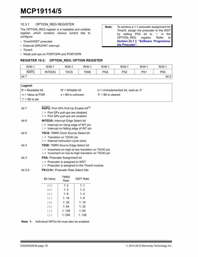
MCP19114/5
10.3.1 OPTION_REG REGISTERThe OPTION_REG register is a readable and writableregister, which contains various control bits toconfigure:• Timer0/WDT prescaler• External GPA2/INT interrupt• Timer0• Weak pull-ups on PORTGPA and PORTGPB
DS20005281B-page 78
Note: To achieve a 1:1 prescaler assignment forTimer0, assign the prescaler to the WDTby setting PSA bit to ‘1’ in theOPTION_REG register. Refer toSection 22.1.3 “Software Programma-ble Prescaler”.
REGISTER 10-2: OPTION_REG: OPTION REGISTER
R/W-1 R/W-1 R/W-1 R/W-1 R/W-1 R/W-1 R/W-1 R/W-1
RAPU INTEDG T0CS T0SE PSA PS2 PS1 PS0bit 7 bit 0
Legend:R = Readable bit W = Writable bit U = Unimplemented bit, read as ‘0’-n = Value at POR x = Bit is unknown ‘0’ = Bit is cleared‘1’ = Bit is set
bit 7 RAPU: Port GPx Pull-Up Enable bit(1)
1 = Port GPx pull-ups are disabled0 = Port GPx pull-ups are enabled
bit 6 INTEDG: Interrupt Edge Select bit0 = Interrupt on rising edge of INT pin1 = Interrupt on falling edge of INT pin
bit 5 T0CS: TMR0 Clock Source Select bit1 = Transition on T0CKI pin0 = Internal instruction cycle clock
bit 4 T0SE: TMR0 Source Edge Select bit1 = Increment on high-to-low transition on T0CKI pin0 = Increment on low-to-high transition on T0CKI pin
bit 3 PSA: Prescaler Assignment bit1 = Prescaler is assigned to WDT0 = Prescaler is assigned to the Timer0 module
bit 2-0 PS<2:0>: Prescaler Rate Select bits
Note 1: Individual WPUx bit must also be enabled.
Bit Value TMR0 Rate WDT Rate
000 1: 2 1: 1001 1: 4 1: 2010 1: 8 1: 4011 1: 16 1: 8100 1: 32 1: 16101 1: 64 1: 32110 1: 128 1: 64111 1: 256 1: 128
2014-2015 Microchip Technology Inc.
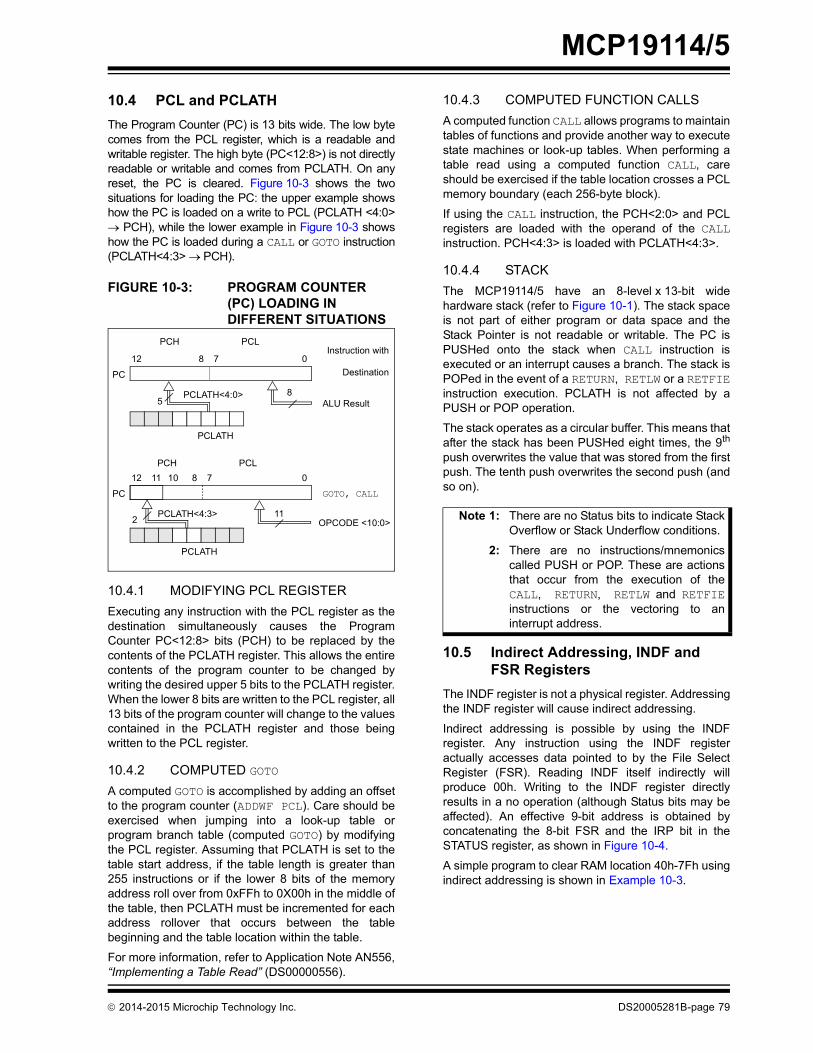
MCP19114/5
10.4 PCL and PCLATHThe Program Counter (PC) is 13 bits wide. The low bytecomes from the PCL register, which is a readable andwritable register. The high byte (PC<12:8>) is not directlyreadable or writable and comes from PCLATH. On anyreset, the PC is cleared. Figure 10-3 shows the twosituations for loading the PC: the upper example showshow the PC is loaded on a write to PCL (PCLATH <4:0> PCH), while the lower example in Figure 10-3 showshow the PC is loaded during a CALL or GOTO instruction(PCLATH<4:3> PCH).FIGURE 10-3: PROGRAM COUNTER (PC) LOADING IN DIFFERENT SITUATIONS
10.4.1 MODIFYING PCL REGISTERExecuting any instruction with the PCL register as thedestination simultaneously causes the ProgramCounter PC<12:8> bits (PCH) to be replaced by thecontents of the PCLATH register. This allows the entirecontents of the program counter to be changed bywriting the desired upper 5 bits to the PCLATH register.When the lower 8 bits are written to the PCL register, all13 bits of the program counter will change to the valuescontained in the PCLATH register and those beingwritten to the PCL register.
10.4.2 COMPUTED GOTOA computed GOTO is accomplished by adding an offsetto the program counter (ADDWF PCL). Care should beexercised when jumping into a look-up table orprogram branch table (computed GOTO) by modifyingthe PCL register. Assuming that PCLATH is set to thetable start address, if the table length is greater than255 instructions or if the lower 8 bits of the memoryaddress roll over from 0xFFh to 0X00h in the middle ofthe table, then PCLATH must be incremented for eachaddress rollover that occurs between the tablebeginning and the table location within the table.
For more information, refer to Application Note AN556,“Implementing a Table Read” (DS00000556).
PC
12 8 7 0
5PCLATH<4:0>
PCLATH
Instruction with
ALU Result
GOTO, CALL
OPCODE <10:0>
8
PC
12 11 10 0
11PCLATH<4:3>
PCH PCL
8 7
2
PCLATH
PCH PCL
Destination
2014-2015 Microchip Technology Inc.
10.4.3 COMPUTED FUNCTION CALLSA computed function CALL allows programs to maintaintables of functions and provide another way to executestate machines or look-up tables. When performing atable read using a computed function CALL, careshould be exercised if the table location crosses a PCLmemory boundary (each 256-byte block).
If using the CALL instruction, the PCH<2:0> and PCLregisters are loaded with the operand of the CALLinstruction. PCH<4:3> is loaded with PCLATH<4:3>.
10.4.4 STACKThe MCP19114/5 have an 8-level x 13-bit widehardware stack (refer to Figure 10-1). The stack spaceis not part of either program or data space and theStack Pointer is not readable or writable. The PC isPUSHed onto the stack when CALL instruction isexecuted or an interrupt causes a branch. The stack isPOPed in the event of a RETURN, RETLW or a RETFIEinstruction execution. PCLATH is not affected by aPUSH or POP operation.
The stack operates as a circular buffer. This means thatafter the stack has been PUSHed eight times, the 9th
push overwrites the value that was stored from the firstpush. The tenth push overwrites the second push (andso on).
10.5 Indirect Addressing, INDF and FSR Registers
The INDF register is not a physical register. Addressingthe INDF register will cause indirect addressing.
Indirect addressing is possible by using the INDFregister. Any instruction using the INDF registeractually accesses data pointed to by the File SelectRegister (FSR). Reading INDF itself indirectly willproduce 00h. Writing to the INDF register directlyresults in a no operation (although Status bits may beaffected). An effective 9-bit address is obtained byconcatenating the 8-bit FSR and the IRP bit in theSTATUS register, as shown in Figure 10-4.
A simple program to clear RAM location 40h-7Fh usingindirect addressing is shown in Example 10-3.
Note 1: There are no Status bits to indicate StackOverflow or Stack Underflow conditions.
2: There are no instructions/mnemonicscalled PUSH or POP. These are actionsthat occur from the execution of theCALL, RETURN, RETLW and RETFIEinstructions or the vectoring to aninterrupt address.
DS20005281B-page 79
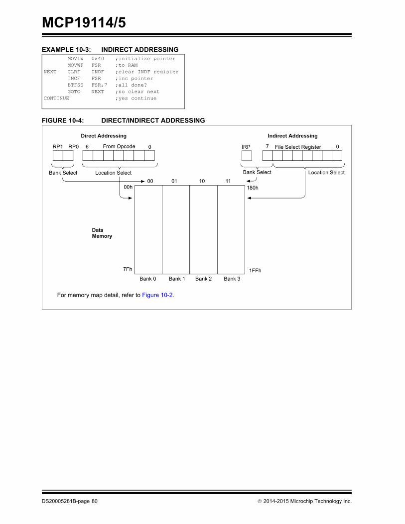
MCP19114/5
EXAMPLE 10-3: INDIRECT ADDRESSINGMOVLW 0x40 ;initialize pointer
MOVWF FSR ;to RAM
NEXT CLRF INDF ;clear INDF register
INCF FSR ;inc pointer
BTFSS FSR,7 ;all done?
GOTO NEXT ;no clear next
CONTINUE ;yes continue
DS20005281B-page 80
FIGURE 10-4: DIRECT/INDIRECT ADDRESSING
DataMemory
Indirect AddressingDirect Addressing
Bank Select Location Select
RP1 RP0 6 0From Opcode IRP File Select Register7 0
Bank Select Location Select00 01 10 11
180h
1FFh
00h
7Fh
Bank 0 Bank 1 Bank 2 Bank 3
For memory map detail, refer to Figure 10-2.
2014-2015 Microchip Technology Inc.

MCP19114/5
11.0 DEVICE CONFIGURATIONDevice Configuration consists of Configuration Word,Code Protection and Device ID.
11.1 Configuration WordThere are several Configuration Word bits that allowdifferent timers to be enabled and memory protectionoptions. These are implemented as ConfigurationWord at 2007h.
2014-2015 Microchip Technology Inc.
Note: The DBGEN bit in Configuration Word ismanaged automatically by devicedevelopment tools, including debuggersand programmers. For normal deviceoperation, this bit should be maintained asa '1'. Debug is available only on theMCP19115.
REGISTER 11-1: CONFIG: CONFIGURATION WORD
R/P-1 U-1 R/P-1 R/P-1 U-1 R/P-1
DBGEN — WRT1 WRT0 — BORENbit 13 bit 8
U-1 R/P-1 R/P-1 R/P-1 R/P-1 U-1 U-1 U-1
— CP MCLRE PWRTE WDTE — — —bit 7 bit 0
Legend:R = Readable bit W = Writable bit U = Unimplemented bit, read as ‘0’-n = Value at POR ‘1’ = Bit is set ‘0’ = Bit is cleared x = Bit is unknown
bit 13 DBGEN: ICD Debug bit1 = ICD debug mode disabled0 = ICD debug mode enabled
bit 12 Unimplemented: Read as ‘0’bit 11-10 WRT<1:0>: Flash Program Memory Self Write Enable bit
11 = Write protection off10 = 000h to 3FFh write protected, 400h to FFFh may be modified by PMCON1 control01 = 000h to 7FFh write protected, 800h to FFFh may be modified by PMCON1 control00 = 000h to FFFh write protected, entire program memory is write protected.
bit 9 Unimplemented: Read as ‘0’bit 8 BOREN: Brown-Out Reset Enable bit
1 = BOR disabled during Sleep and Enabled during operation0 = BOR disabled
bit 7 Unimplemented: Read as ‘0’
bit 6 CP: Code Protection1 = Program memory is not code protected0 = Program memory is external read and write protected
bit 5 MCLRE: MCLR Pin Function Select1 = MCLR pin is MCLR function and weak internal pull-up is enabled0 = MCLR pin is alternate function, MCLR function is internally disabled
bit 4 PWRTE: Power-Up Timer Enable bit(1)
1 = PWRT disabled0 = PWRT enabled
bit 3 WDTE: Watchdog Timer Enable bit1 = WDT enabled0 = WDT disabled
bit 2-0 Unimplemented: Read as ‘0’
Note 1: Bit is reserved and not controlled by user.
DS20005281B-page 81
MCP19114/5
11.2 Code ProtectionCode protection allows the device to be protected fromunauthorized access. Internal access to the programmemory is unaffected by any code protection setting.11.2.1 PROGRAM MEMORY PROTECTIONThe entire program memory space is protected fromexternal reads and writes by the CP bit in theConfiguration Word. When CP = 0, external reads andwrites of program memory are inhibited and a read willreturn all ‘0’s. The CPU can continue to read programmemory, regardless of the protection bit settings.Writing the program memory is dependent upon thewrite protection setting. Refer to Section 11.3 “WriteProtection” for more information.
11.3 Write ProtectionWrite protection allows the device to be protected fromunintended self-writes. Applications, such as bootloader software, can be protected while allowing otherregions of the program memory to be modified.
The WRT<1:0> bits in the Configuration Word definethe size of the program memory block that is protected.
11.4 ID LocationsFour memory locations (2000h-2003h) are designatedas ID locations where the user can store checksum orother code identification numbers. These locations arenot accessible during normal execution but arereadable and writable during Program/Verify mode.Only the Least Significant 7 bits of the ID locations arereported when using MPLAB Integrated DevelopmentEnvironment (IDE).
DS20005281B-page 82
2014-2015 Microchip Technology Inc.
MCP19114/5
12.0 OSCILLATOR MODESThe MCP19114/5 have one oscillator configurationwhich is an 8 MHz internal oscillator.
12.1 Internal Oscillator (INTOSC)The Internal Oscillator module provides a systemclock source of 8 MHz. The frequency of the internaloscillator can be trimmed with a calibration value in theOSCTUNE register.
2014-2015 Microchip Technology Inc.
12.2 Oscillator CalibrationThe 8 MHz internal oscillator is factory-calibrated. Thefactory calibration values reside in the read-onlyCALWD6 register. These values must be read from theCALWD6 register and stored in the OSCCAL register.Refer to Section 17.0 “Flash Program MemoryControl” for the procedure on reading the programmemory.
12.3 Frequency Tuning in User ModeIn addition to the factory calibration, the basefrequency can be tuned in the user's application. Thisfrequency tuning capability allows the user to deviatefrom the factory-calibrated frequency. The user cantune the frequency by writing to the OSCTUNEregister (refer to Register 12-1).
Note: The FCAL<6:0> bits in the CALWD6register must be written into the OSCCALregister to calibrate the internal oscillator.
REGISTER 12-1: OSCTUNE: OSCILLATOR TUNING REGISTER
U-0 U-0 U-0 R/W-0 R/W-0 R/W-0 R/W-0 R/W-0 — — — TUN4 TUN3 TUN2 TUN1 TUN0
bit 7 bit 0
Legend:R = Readable bit W = Writable bit U = Unimplemented bit, read as ‘0’-n = Value at POR ‘1’ = Bit is set ‘0’ = Bit is cleared x = Bit is unknown
bit 7-5 Unimplemented: Read as ‘0’bit 4-0 TUN<4:0>: Frequency Tuning bits
01111 = Maximum frequency01110 = •••00001 = 00000 = Center frequency. Oscillator Module is running at the calibrated frequency.11111 = •••10000 = Minimum frequency
DS20005281B-page 83

MCP19114/5
12.3.1 OSCILLATOR DELAY UPONPOWER-UP, WAKE-UP AND BASE FREQUENCY CHANGE
In applications where the OSCTUNE register is used toshift the frequency of the internal oscillator, theapplication should not expect the frequency of theinternal oscillator to stabilize immediately. In this case,the frequency may shift gradually toward the newvalue. The time for this frequency shift is less than eightcycles of the base frequency.
On power-up, the device is held in reset by thepower-up time if the power-up timer is enabled.
Following a wake-up from Sleep mode or POR, aninternal delay of ~10 µs is invoked to allow the memorybias to stabilize before program execution can begin.
DS20005281B-page 84
TABLE 12-1: SUMMARY OF REGISTERS ASSOCIATED WITH CLOCK SOURCES
Name Bit 7 Bit 6 Bit 5 Bit 4 Bit 3 Bit 2 Bit 1 Bit 0 Register on Page
OSCTUNE — — — TUN4 TUN3 TUN2 TUN1 TUN0 83Legend: — = unimplemented locations, read as ‘0’. Shaded cells are not used by clock sources.
TABLE 12-2: SUMMARY OF CONFIGURATION WORD ASSOCIATED WITH CLOCK SOURCES
Name Bits Bit -/7 Bit -/6 Bit 13/5 Bit 12/4 Bit 11/3 Bit 10/2 Bit 9/1 Bit 8/0 Register on Page
CONFIG613:8 — — — — — — — —
627:0 — FCAL6 FCAL5 FCAL4 FCAL3 FCAL2 FCAL1 FCAL0
Legend: — = unimplemented locations, read as ‘0’. Shaded cells are not used by clock sources.
2014-2015 Microchip Technology Inc.
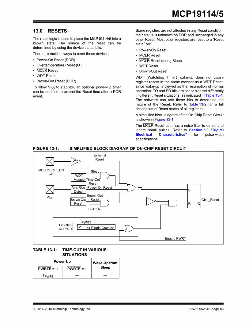
MCP19114/5
13.0 RESETSThe reset logic is used to place the MCP19114/5 into aknown state. The source of the reset can bedetermined by using the device status bits.
There are multiple ways to reset these devices:
• Power-On Reset (POR)• Overtemperature Reset (OT)• MCLR Reset• WDT Reset• Brown-Out Reset (BOR)
To allow VDD to stabilize, an optional power-up timercan be enabled to extend the Reset time after a PORevent.
2014-2015 Microchip Technology Inc.
Some registers are not affected in any Reset condition;their status is unknown on POR and unchanged in anyother Reset. Most other registers are reset to a “Resetstate” on:
• Power-On Reset• MCLR Reset• MCLR Reset during Sleep• WDT Reset• Brown-Out Reset
WDT (Watchdog Timer) wake-up does not causeregister resets in the same manner as a WDT Reset,since wake-up is viewed as the resumption of normaloperation. TO and PD bits are set or cleared differentlyin different Reset situations, as indicated in Table 13-1.The software can use these bits to determine thenature of the Reset. Refer to Table 13-2 for a fulldescription of Reset states of all registers.
A simplified block diagram of the On-Chip Reset Circuitis shown in Figure 13-1.
The MCLR Reset path has a noise filter to detect andignore small pulses. Refer to Section 5.0 “DigitalElectrical Characteristics” for pulse-widthspecifications.
FIGURE 13-1: SIMPLIFIED BLOCK DIAGRAM OF ON-CHIP RESET CIRCUIT
WDTModule
VDD RiseDetect
Brown-OutReset
Sleep
BOREN
MCLR/TEST_EN pin
VDD
External Reset
S
R Q
On-ChipRC OSC 11-bit Ripple Counter
PWRT
Enable PWRT
Chip_Reset
Power-On Reset
Time-Out Reset
Brown-OutReset
TABLE 13-1: TIME-OUT IN VARIOUS SITUATIONS
Power-Up Wake-Up from SleepPWRTE = 0 PWRTE = 1
TPWRT — —
DS20005281B-page 85
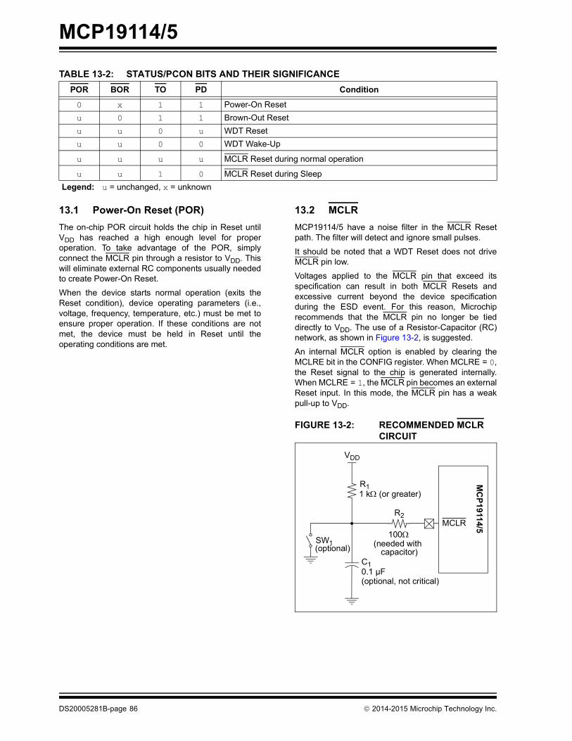
MCP19114/5
TABLE 13-2: STATUS/PCON BITS AND THEIR SIGNIFICANCEPOR BOR TO PD Condition
0 x 1 1 Power-On Resetu 0 1 1 Brown-Out Resetu u 0 u WDT Resetu u 0 0 WDT Wake-Up
u u u u MCLR Reset during normal operation
u u 1 0 MCLR Reset during SleepLegend: u = unchanged, x = unknown
13.1 Power-On Reset (POR)The on-chip POR circuit holds the chip in Reset untilVDD has reached a high enough level for properoperation. To take advantage of the POR, simplyconnect the MCLR pin through a resistor to VDD. Thiswill eliminate external RC components usually neededto create Power-On Reset.
When the device starts normal operation (exits theReset condition), device operating parameters (i.e.,voltage, frequency, temperature, etc.) must be met toensure proper operation. If these conditions are notmet, the device must be held in Reset until theoperating conditions are met.
DS20005281B-page 86
13.2 MCLRMCP19114/5 have a noise filter in the MCLR Resetpath. The filter will detect and ignore small pulses.
It should be noted that a WDT Reset does not driveMCLR pin low.
Voltages applied to the MCLR pin that exceed itsspecification can result in both MCLR Resets andexcessive current beyond the device specificationduring the ESD event. For this reason, Microchiprecommends that the MCLR pin no longer be tieddirectly to VDD. The use of a Resistor-Capacitor (RC)network, as shown in Figure 13-2, is suggested.
An internal MCLR option is enabled by clearing theMCLRE bit in the CONFIG register. When MCLRE = 0,the Reset signal to the chip is generated internally.When MCLRE = 1, the MCLR pin becomes an externalReset input. In this mode, the MCLR pin has a weakpull-up to VDD.
FIGURE 13-2: RECOMMENDED MCLR CIRCUIT
VDD
MCLR
R11 k (or greater)
C10.1 µF(optional, not critical)
R2
100(needed with SW1
(optional)
MC
P19114/5
capacitor)
2014-2015 Microchip Techn
ology Inc.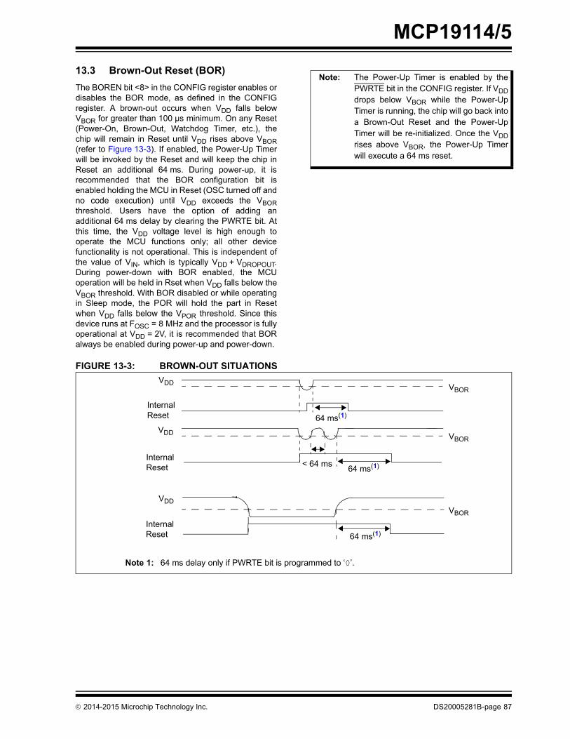
MCP19114/5
13.3 Brown-Out Reset (BOR)The BOREN bit <8> in the CONFIG register enables ordisables the BOR mode, as defined in the CONFIGregister. A brown-out occurs when VDD falls belowVBOR for greater than 100 µs minimum. On any Reset(Power-On, Brown-Out, Watchdog Timer, etc.), thechip will remain in Reset until VDD rises above VBOR(refer to Figure 13-3). If enabled, the Power-Up Timerwill be invoked by the Reset and will keep the chip inReset an additional 64 ms. During power-up, it isrecommended that the BOR configuration bit isenabled holding the MCU in Reset (OSC turned off andno code execution) until VDD exceeds the VBORthreshold. Users have the option of adding anadditional 64 ms delay by clearing the PWRTE bit. Atthis time, the VDD voltage level is high enough tooperate the MCU functions only; all other devicefunctionality is not operational. This is independent ofthe value of VIN, which is typically VDD + VDROPOUT.During power-down with BOR enabled, the MCUoperation will be held in Rset when VDD falls below theVBOR threshold. With BOR disabled or while operatingin Sleep mode, the POR will hold the part in Resetwhen VDD falls below the VPOR threshold. Since thisdevice runs at FOSC = 8 MHz and the processor is fullyoperational at VDD = 2V, it is recommended that BORalways be enabled during power-up and power-down.2014-2015 Microchip Technology Inc.
Note: The Power-Up Timer is enabled by thePWRTE bit in the CONFIG register. If VDDdrops below VBOR while the Power-UpTimer is running, the chip will go back intoa Brown-Out Reset and the Power-UpTimer will be re-initialized. Once the VDDrises above VBOR, the Power-Up Timerwill execute a 64 ms reset.
FIGURE 13-3: BROWN-OUT SITUATIONS
VDD
InternalReset
VDD
VDD
InternalReset
InternalReset
VBOR
VBOR
VBOR
64 ms(1)
64 ms(1)
64 ms(1)
< 64 ms
Note 1: 64 ms delay only if PWRTE bit is programmed to ‘0’.
DS
20005281B-page 87
MCP19114/5
13.4 Power-Up Timer (PWRT)The Power-Up Timer provides a fixed 64 ms (nominal)time-out on power-up only, from POR Reset. ThePower-Up Timer operates from an internal RCoscillator. The chip is kept in Reset as long as PWRT isactive. The PWRT delay allows the VDD to rise to anacceptable level. A bit (PWRTE) in the CONFIGregister can disable (if set) or enable (if cleared orprogrammed) the Power-Up Timer.The Power-Up Timer delay will vary from chip to chipdue to:
• VDD variation• Temperature variation• Process variation
The Power-Up Timer optionally delays device executionafter a POR event. This timer is typically used to allowVDD to stabilize before allowing the device to startrunning.
The Power-Up Timer is controlled by the PWRTE bit inthe CONFIG register.
Note: Voltage spikes below VSS at the MCLRpin, inducing currents greater than 80 mA,may cause latch-up. Thus, a seriesresistor of 50-100 should be used whenapplying a “low” level to the MCLR pin,rather than pulling this pin directly to VSS.
DS20005281B-page 88
13.5 Watchdog Timer (WDT) ResetThe Watchdog Timer generates a Reset if the firmwaredoes not issue a CLRWDT instruction within the time-outperiod. The TO and PD bits in the STATUS register arechanged to indicate the WDT Reset. Refer toSection 16.0 “Watchdog Timer (WDT)” for moreinformation.
13.6 Start-Up SequenceUpon the release of a POR, the following must occurbefore the device begins executing:
• Power-Up Timer runs to completion (if enabled)• Oscillator start-up timer runs to completion• MCLR must be released (if enabled)
The total time out will vary based on PWRTE bit status.For example, with PWRTE bit erased (PWRT disabled),there will be no time out at all. Figures 13-4, 13-5and 13-6 depict time-out sequences.
Since the time outs occur from the POR pulse, if MCLRis kept low long enough, the time-outs will expire. Then,bringing MCLR high will begin execution immediately(refer to Figure 13-5). This is useful for testing purposesor to synchronize more than one MCP19114/5 deviceoperating in parallel.
13.6.1 POWER CONTROL (PCON) REGISTER
The Power Control (PCON) register (address 8Eh) hastwo Status bits to indicate what type of Reset occurredlast.
FIGURE 13-4: TIME-OUT SEQUENCE ON POWER-UP (DELAYED MCLR): CASE 1
TPWRT
TIOSCST
VDD
MCLR
Internal POR
PWRT Time-Out
OST Time-Out
Internal Reset
2014-2015 Microchip Technology Inc.
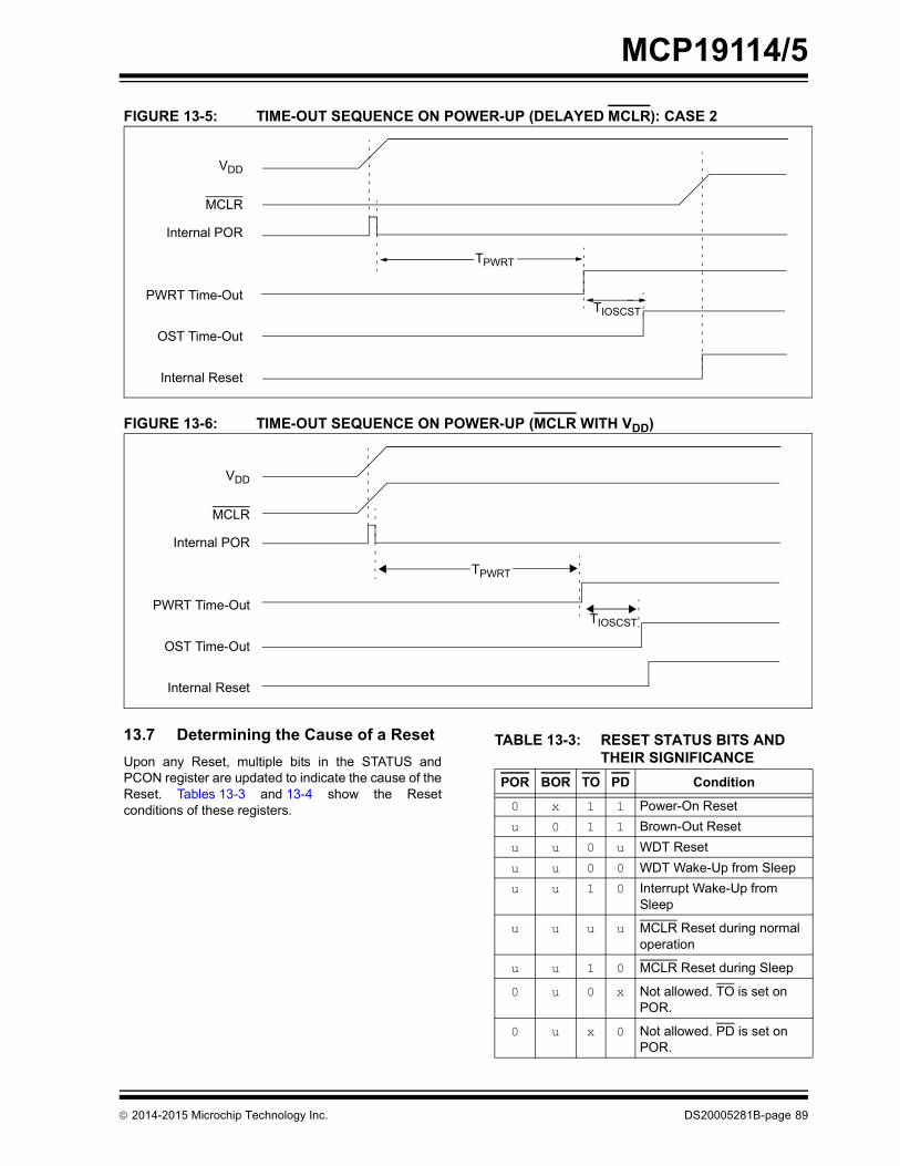
MCP19114/5
FIGURE 13-5: TIME-OUT SEQUENCE ON POWER-UP (DELAYED MCLR): CASE 2
FIGURE 13-6: TIME-OUT SEQUENCE ON POWER-UP (MCLR WITH VDD)
VDD
MCLR
Internal POR
PWRT Time-Out
OST Time-Out
Internal Reset
TPWRT
TIOSCST
VDD
MCLR
Internal POR
PWRT Time-Out
OST Time-Out
Internal Reset
TPWRT
TIOSCST
13.7 Determining the Cause of a ResetUpon any Reset, multiple bits in the STATUS andPCON register are updated to indicate the cause of theReset. Tables 13-3 and 13-4 show the Resetconditions of these registers.
2014-2015 Microchip Technology Inc.
TABLE 13-3: RESET STATUS BITS AND THEIR SIGNIFICANCE
POR BOR TO PD Condition
0 x 1 1 Power-On Resetu 0 1 1 Brown-Out Resetu u 0 u WDT Reset u u 0 0 WDT Wake-Up from Sleepu u 1 0 Interrupt Wake-Up from
Sleep
u u u u MCLR Reset during normal operation
u u 1 0 MCLR Reset during Sleep
0 u 0 x Not allowed. TO is set on POR.
0 u x 0 Not allowed. PD is set on POR.
DS20005281B-page 89
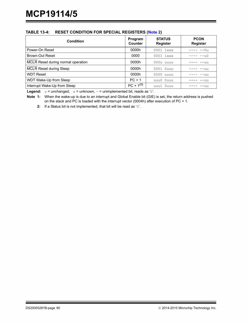
MCP19114/5
TABLE 13-4: RESET CONDITION FOR SPECIAL REGISTERS (Note 2)
Condition ProgramCounter
STATUSRegister
PCONRegister
Power-On Reset 0000h 0001 1xxx ---- --0u
Brown-Out Reset 0000 0001 1xxx ---- --u0
MCLR Reset during normal operation 0000h 000u uuuu ---- --uu
MCLR Reset during Sleep 0000h 0001 0uuu ---- --uu
WDT Reset 0000h 0000 uuuu ---- --uu
WDT Wake-Up from Sleep PC + 1 uuu0 0uuu ---- --uu
Interrupt Wake-Up from Sleep PC + 1(1) uuu1 0uuu ---- --uu
Legend: u = unchanged, x = unknown, - = unimplemented bit, reads as ‘0’.Note 1: When the wake-up is due to an interrupt and Global Enable bit (GIE) is set, the return address is pushed
on the stack and PC is loaded with the interrupt vector (0004h) after execution of PC + 1.2: If a Status bit is not implemented, that bit will be read as ‘0’.
DS20005281B-page 90 2014-2015 Microchip Technology Inc.
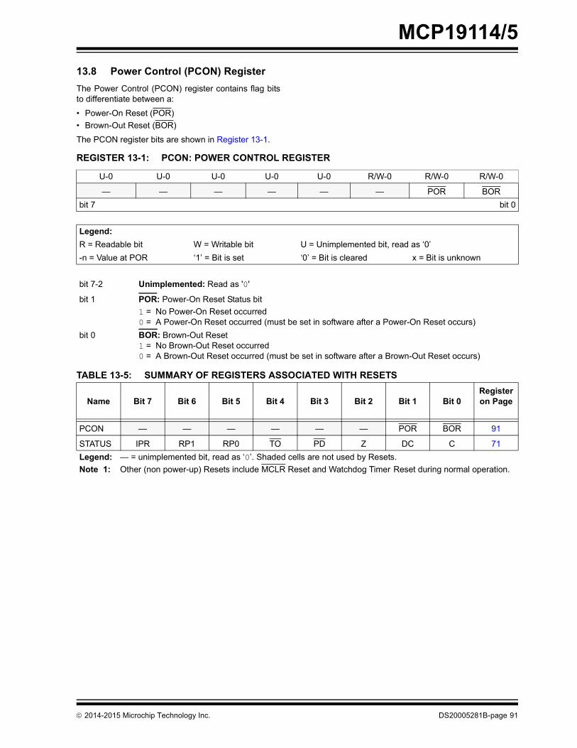
MCP19114/5
13.8 Power Control (PCON) Register The Power Control (PCON) register contains flag bitsto differentiate between a:• Power-On Reset (POR)• Brown-Out Reset (BOR)
The PCON register bits are shown in Register 13-1.
2014-2015 Microchip Technology Inc.
REGISTER 13-1: PCON: POWER CONTROL REGISTER
U-0 U-0 U-0 U-0 U-0 R/W-0 R/W-0 R/W-0
— — — — — — POR BORbit 7 bit 0
Legend:R = Readable bit W = Writable bit U = Unimplemented bit, read as ‘0’-n = Value at POR ‘1’ = Bit is set ‘0’ = Bit is cleared x = Bit is unknown
bit 7-2 Unimplemented: Read as '0'
bit 1 POR: Power-On Reset Status bit1 = No Power-On Reset occurred0 = A Power-On Reset occurred (must be set in software after a Power-On Reset occurs)
bit 0 BOR: Brown-Out Reset 1 = No Brown-Out Reset occurred 0 = A Brown-Out Reset occurred (must be set in software after a Brown-Out Reset occurs)
TABLE 13-5: SUMMARY OF REGISTERS ASSOCIATED WITH RESETS
Name Bit 7 Bit 6 Bit 5 Bit 4 Bit 3 Bit 2 Bit 1 Bit 0Register on Page
PCON — — — — — — POR BOR 91
STATUS IPR RP1 RP0 TO PD Z DC C 71Legend: — = unimplemented bit, read as ‘0’. Shaded cells are not used by Resets.Note 1: Other (non power-up) Resets include MCLR Reset and Watchdog Timer Reset during normal operation.
DS20005281B-page 91

MCP19114/5
NOTES:DS20005281B-page 92
2014-2015 Microchip Technology Inc.
MCP19114/5
14.0 INTERRUPTSThe MCP19114/5 have multiple sources of interrupt:
• External Interrupt (INT pin)• Interrupt-On-Change (IOC) Interrupts• Timer0 Overflow Interrupt• Timer1 Overflow Interrupt• Timer2 Match Interrupt• ADC Interrupt• System Input Undervoltage Error• System Input Overvoltage Error• SSP• BCL• Desaturation Detection• Gate Drive UVLO• Capture/Compare 1• Capture/Compare 2• Overtemperature
The Interrupt Control (INTCON) register and thePeripheral Interrupt Request (PIRx) registers recordindividual interrupt requests in flag bits. The INTCONregister also has individual and global interrupt enablebits.
The Global Interrupt Enable bit, GIE, in the INTCONregister enables (if set) all unmasked interrupts ordisables (if cleared) all interrupts. Individual interruptscan be disabled through their corresponding enablebits in the INTCON register and PIEx registers. GIE iscleared on Reset.
When an interrupt is serviced, the following actionsoccur automatically:
• The GIE is cleared to disable any further interrupt• The return address is pushed onto the stack• The PC is loaded with 0004h
The firmware within the Interrupt Service Routine (ISR)should determine the source of the interrupt by pollingthe interrupt flag bits. The interrupt flag bits must becleared before exiting the ISR to avoid repeatedinterrupts. Because the GIE bit is cleared, any interruptthat occurs while executing the ISR will be recordedthrough its interrupt flag but will not cause theprocessor to redirect to the interrupt vector.
Note 1: Individual interrupt flag bits are set,regardless of the status of theircorresponding mask bit or the GIE bit.
2: When an instruction that clears the GIEbit is executed, any interrupts that werepending for execution in the next cycleare ignored. The interrupts which wereignored are still pending to be servicedwhen the GIE bit is set again.
2014-2015 Microchip Technology Inc.
The RETFIE instruction exits the ISR by popping theprevious address from the stack, restoring the savedcontext from the shadow registers and setting the GIE bit.
For additional information on a specific interrupt’soperation, refer to its peripheral chapter.
14.1 Interrupt LatencyFor external interrupt events, such as the INT pin orPORTGPx change interrupt, the interrupt latency willbe three or four instruction cycles. The exact latencydepends upon when the interrupt event occurs (refer toFigure 14-2). The latency is the same for one- ortwo-cycle instructions.
14.2 GPA2/INT InterruptThe external interrupt on the GPA2/INT pin isedge-triggered, either on the rising edge if the INTEDGbit in the OPTION_REG register is set, or the fallingedge if the INTEDG bit is clear. When a valid edgeappears on the GPA2/INT pin, the INTF bit in theINTCON register is set. This interrupt can be disabledby clearing the INTE control bit in the INTCON register.The INTF bit must be cleared by software in theInterrupt Service Routine before re-enabling thisinterrupt. The GPA2/INT interrupt can wake up theprocessor from Sleep, if the INTE bit was set prior togoing into Sleep. Refer to Section 15.0 “Power-DownMode (Sleep)” for details on Sleep and Section 15.1“Wake-Up from Sleep” for timing of wake-up fromSleep through GPA2/INT interrupt.
Note: The ANSEL register must be initialized toconfigure an analog channel as a digitalinput. Pins configured as analog inputswill read ‘0’ and cannot generate aninterrupt.
DS20005281B-page 93
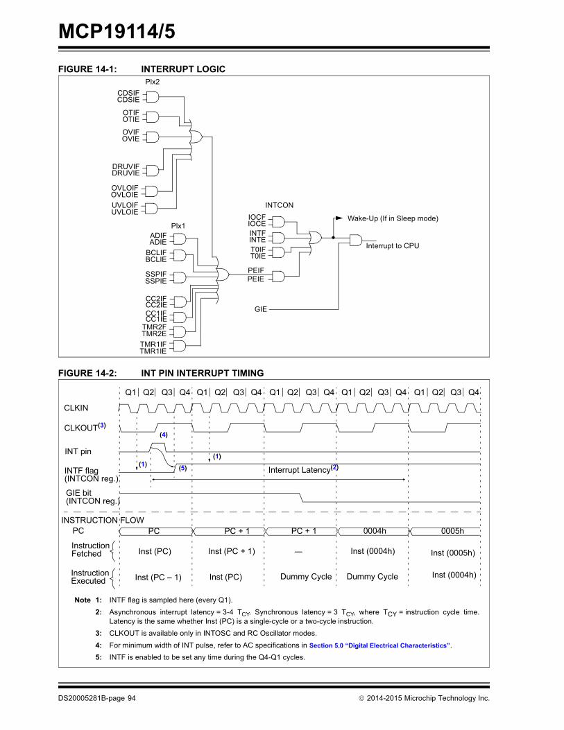
MCP19114/5
FIGURE 14-1: INTERRUPT LOGICFIGURE 14-2: INT PIN INTERRUPT TIMING
TMR1IFTMR1IE
SSPIFSSPIE
IOCFIOCEINTFINTE
GIE
PEIE
Wake-Up (If in Sleep mode)
Interrupt to CPU
PEIF
ADIFADIE
CDSIFCDSIE
OTIFOTIE
OVIFOVIE
DRUVIFDRUVIE
BCLIFBCLIE
TMR2FTMR2E
T0IFT0IE
Plx2
UVLOIFUVLOIE
OVLOIFOVLOIE
Plx1
CC2IFCC2IECC1IFCC1IE
INTCON
Q2Q1 Q3 Q4 Q2Q1 Q3 Q4 Q2Q1 Q3 Q4 Q2Q1 Q3 Q4 Q2Q1 Q3 Q4
CLKIN
INT pin
INTF flag(INTCON reg.)
GIE bit(INTCON reg.)
INSTRUCTION FLOWPC
InstructionFetched
InstructionExecuted
PC PC + 1 PC + 1 0004h 0005h
Inst (0004h) Inst (0005h)
Dummy Cycle
Inst (PC) Inst (PC + 1)
Inst (PC – 1) Inst (0004h)Dummy CycleInst (PC)
—
Note 1: INTF flag is sampled here (every Q1).2: Asynchronous interrupt latency = 3-4 TCY. Synchronous latency = 3 TCY, where TCY = instruction cycle time.
Latency is the same whether Inst (PC) is a single-cycle or a two-cycle instruction.3: CLKOUT is available only in INTOSC and RC Oscillator modes.4: For minimum width of INT pulse, refer to AC specifications in Section 5.0 “Digital Electrical Characteristics”.5: INTF is enabled to be set any time during the Q4-Q1 cycles.
CLKOUT(3)(4)
(1) (5)
(1)
Interrupt Latency(2)
D
S20005281B-page 94 2014-2015 Microchip Technology Inc.
MCP19114/5
14.3 Interrupt Control Registers14.3.1 INTCON REGISTERThe INTCON register is a readable and writableregister that contains the various enable and flag bitsfor the TMR0 register overflow, interrupt-on-changeand external INT pin interrupts.
2014-2015 Microchip Technology Inc.
Note: Interrupt flag bits are set when an interruptcondition occurs, regardless of the state ofits corresponding enable bit or the GlobalEnable bit, GIE, in the INTCON register.The user’s software should ensure theappropriate interrupt flag bits are clearprior to enabling an interrupt.
REGISTER 14-1: INTCON: INTERRUPT CONTROL REGISTER
R/W-0 R/W-0 R/W-0 R/W-0 R/W-0 R/W-0 R/W-0 R/W-xGIE PEIE T0IE INTE IOCE T0IF INTF IOCF
bit 7 bit 0
Legend:R = Readable bit W = Writable bit U = Unimplemented bit, read as ‘0’-n = Value at POR ‘1’ = Bit is set ‘0’ = Bit is cleared x = Bit is unknown
bit 7 GIE: Global Interrupt Enable bit1 = Enables all unmasked interrupts0 = Disables all interrupts
bit 6 PEIE: Peripheral Interrupt Enable bit1 = Enables all unmasked peripheral interrupts0 = Disables all peripheral interrupts
bit 5 T0IE: TMR0 Overflow Interrupt Enable bit1 = Enables the TMR0 interrupt0 = Disables the TMR0 interrupt
bit 4 INTE: INT External Interrupt Enable bit1 = Enables the INT external interrupt0 = Disables the INT external interrupt
bit 3 IOCE: Interrupt-on-Change Enable bit(1)
1 = Enables the interrupt-on-change0 = Disables the interrupt-on-change
bit 2 T0IF: TMR0 Overflow Interrupt Flag bit(2)
1 = TMR0 register has overflowed (must be cleared in software)0 = TMR0 register did not overflow
bit 1 INTF: External Interrupt Flag bit1 = The external interrupt occurred (must be cleared in software)0 = The external interrupt did not occur
bit 0 IOCF: Interrupt-on-Change Interrupt Flag bit1 = When at least one of the interrupt-on-change pins changed state0 = None of the interrupt-on-change pins have changed state
Note 1: IOCx registers must also be enabled.2: T0IF bit is set when TMR0 rolls over. TMR0 is unchanged on Reset and should be initialized before
clearing T0IF bit.
DS20005281B-page 95

MCP19114/5
14.3.1.1 PIE1 RegisterThe PIE1 register contains the Peripheral InterruptEnable bits, as shown in Register 14-2.DS20005281B-page 96
Note 1: Bit PEIE in the INTCON register must beset to enable any peripheral interrupt.
REGISTER 14-2: PIE1: PERIPHERAL INTERRUPT ENABLE REGISTER 1
U-0 R/W-0 R/W-0 R/W-0 R/W-0 R/W-0 R/W-0 R/W-0— ADIE BCLIE SSPIE CC2IE CC1IE TMR2IE TMR1IE
bit 7 bit 0
Legend:R = Readable bit W = Writable bit U = Unimplemented bit, read as ‘0’-n = Value at POR ‘1’ = Bit is set ‘0’ = Bit is cleared x = Bit is unknown
bit 7 Unimplemented: Read as ‘0’bit 6 ADIE: ADC Interrupt Enable bit
1 = Enables the ADC interrupt0 = Disables the ADC interrupt
bit 5 BCLIE: MSSP Bus Collision Interrupt Enable bit1 = Enables the MSSP Bus Collision Interrupt0 = Disables the MSSP Bus Collision Interrupt
bit 4 SSPIE: Synchronous Serial Port (MSSP) Interrupt Enable bit1 = Enables the MSSP interrupt0 = Disables the MSSP interrupt
bit 3 CC2IE: Capture2/Compare2 Interrupt Enable bit 1 = Enables the Capture2/Compare2 interrupt0 = Disables the Capture2/Compare2 interrupt
bit 2 CC1IE: Capture1/Compare1 Interrupt Enable bit 1 = Enables the Capture1/Compare1 interrupt0 = Disables the Capture1/Compare1 interrupt
bit 1 TMR2IE: Timer2 Interrupt Enable1 = Enables the Timer2 interrupt0 = Disables the Timer2 interrupt
bit 0 TMR1IE: Timer1 Interrupt Enable1 = Enables the Timer1 interrupt0 = Disables the Timer1 interrupt
2014-2015 Microchip Technology Inc.

MCP19114/5
14.3.1.2 PIE2 RegisterThe PIE2 register contains the Peripheral InterruptEnable bits, as shown in Register 14-3.2014-2015 Microchip Technology Inc.
Note 1: Bit PEIE in the INTCON register must beset to enable any peripheral interrupt.
REGISTER 14-3: PIE2: PERIPHERAL INTERRUPT ENABLE REGISTER 2
R/W-0 U-0 U-0 R/W-0 R/W-0 R/W-0 R/W-0 R/W-0CDSIE — — OTIE OVIE DRUVIE OVLOIE UVLOIE
bit 7 bit 0
Legend:R = Readable bit W = Writable bit U = Unimplemented bit, read as ‘0’-n = Value at POR ‘1’ = Bit is set ‘0’ = Bit is cleared x = Bit is unknown
bit 7 CDSIE: Desaturation Detection Interrupt Enable bit 1 = Enables the DESAT Detect interrupt0 = Disables the DESAT Detect interrupt
bit 6-5 Unimplemented: Read as ‘0’bit 4 OTIE: Overtemperature Interrupt Enable bit
1 = Enables overtemperature interrupt0 = Disables overtemperature interrupt
bit 3 OVIE: VOUT Overvoltage Interrupt Enable bit 1 = Enables the OV interrupt0 = Disables the OV interrupt
bit 2 DRUVIE: Gate Drive Undervoltage Lockout Interrupt Enable bit1 = Enables Gate Drive UVLO interrupt0 = Disables Gate Drive UVLO interrupt
bit 1 OVLOIE: VIN Overvoltage Lockout Interrupt Enable bit1 = Enables OVLO interrupt0 = Disables OVLO interrupt
bit 0 UVLOIE: VIN Undervoltage Lockout Interrupt Enable bit1 = Enables UVLO interrupt0 = Disables UVLO interrupt
DS20005281B-page 97
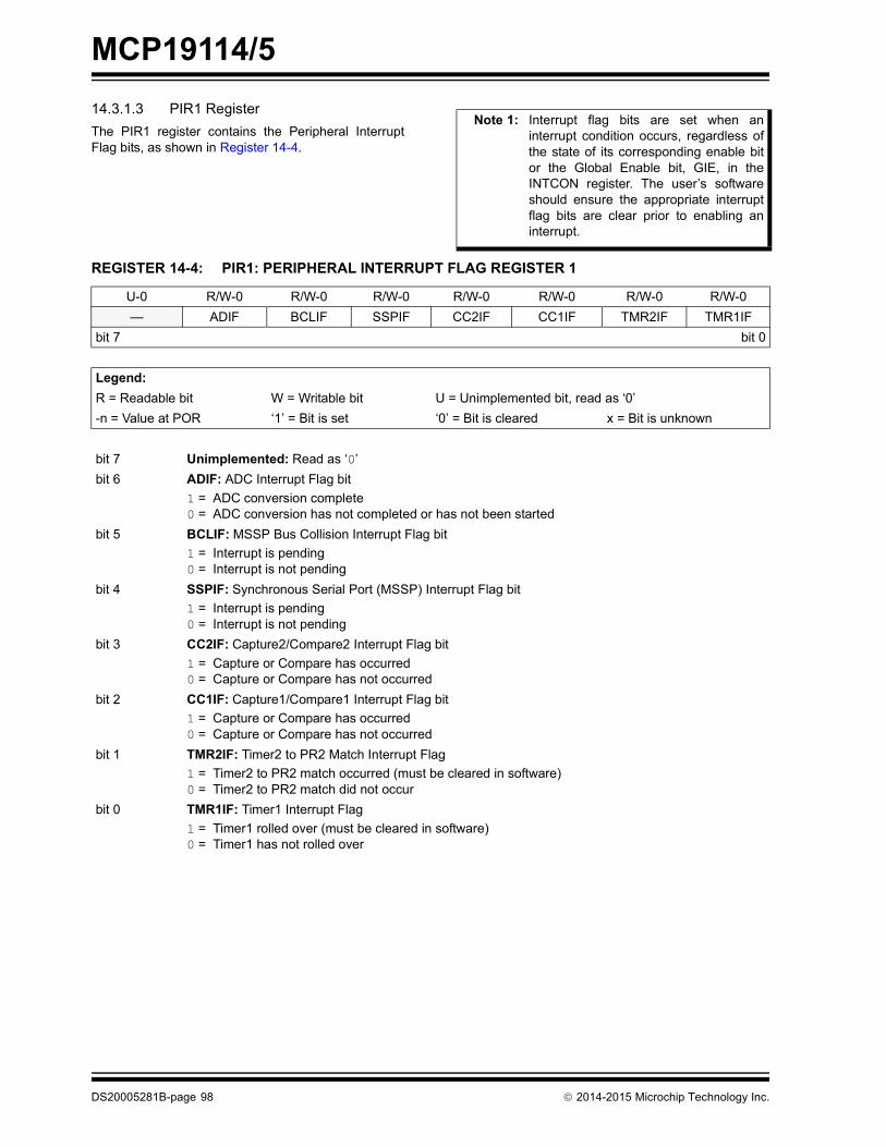
MCP19114/5
14.3.1.3 PIR1 RegisterThe PIR1 register contains the Peripheral InterruptFlag bits, as shown in Register 14-4.DS20005281B-page 98
Note 1: Interrupt flag bits are set when aninterrupt condition occurs, regardless ofthe state of its corresponding enable bitor the Global Enable bit, GIE, in theINTCON register. The user’s softwareshould ensure the appropriate interruptflag bits are clear prior to enabling aninterrupt.
REGISTER 14-4: PIR1: PERIPHERAL INTERRUPT FLAG REGISTER 1
U-0 R/W-0 R/W-0 R/W-0 R/W-0 R/W-0 R/W-0 R/W-0— ADIF BCLIF SSPIF CC2IF CC1IF TMR2IF TMR1IF
bit 7 bit 0
Legend:R = Readable bit W = Writable bit U = Unimplemented bit, read as ‘0’-n = Value at POR ‘1’ = Bit is set ‘0’ = Bit is cleared x = Bit is unknown
bit 7 Unimplemented: Read as ‘0’bit 6 ADIF: ADC Interrupt Flag bit
1 = ADC conversion complete0 = ADC conversion has not completed or has not been started
bit 5 BCLIF: MSSP Bus Collision Interrupt Flag bit1 = Interrupt is pending0 = Interrupt is not pending
bit 4 SSPIF: Synchronous Serial Port (MSSP) Interrupt Flag bit 1 = Interrupt is pending0 = Interrupt is not pending
bit 3 CC2IF: Capture2/Compare2 Interrupt Flag bit1 = Capture or Compare has occurred0 = Capture or Compare has not occurred
bit 2 CC1IF: Capture1/Compare1 Interrupt Flag bit1 = Capture or Compare has occurred0 = Capture or Compare has not occurred
bit 1 TMR2IF: Timer2 to PR2 Match Interrupt Flag1 = Timer2 to PR2 match occurred (must be cleared in software)0 = Timer2 to PR2 match did not occur
bit 0 TMR1IF: Timer1 Interrupt Flag1 = Timer1 rolled over (must be cleared in software)0 = Timer1 has not rolled over
2014-2015 Microchip Technology Inc.
MCP19114/5
14.3.1.4 PIR2 RegisterThe PIR2 register contains the Peripheral InterruptFlag bits, as shown in Register 14-3.2014-2015 Microchip Technology Inc.
Note 1: Interrupt flag bits are set when aninterrupt condition occurs, regardless ofthe state of its corresponding enable bitor the Global Enable bit, GIE, in theINTCON register. The user’s softwareshould ensure the appropriate interruptflag bits are clear prior to enabling aninterrupt.
REGISTER 14-5: PIR2: PERIPHERAL INTERRUPT FLAG REGISTER 2
R/W-0 U-0 U-0 R/W-0 R/W-0 R/W-0 R/W-0 R/W-0CDSIF — — OTIF OVIF DRUVIF OVLOIF UVLOIF
bit 7 bit 0
Legend:R = Readable bit W = Writable bit U = Unimplemented bit, read as ‘0’-n = Value at POR ‘1’ = Bit is set ‘0’ = Bit is cleared x = Bit is unknown
bit 7 CDSIF: DESAT Detect comparator module interrupt flag bit1 = An interrupt is pending0 = An interrupt is not pending
bit 6-5 Unimplemented: Read as ‘0’bit 4 OTIF: Overtemperature Interrupt Flag bit
1 = Overtemperature event has occurred0 = Overtemperature event has not occurred
bit 3 OVIF: Overvoltage Interrupt Flag bitWith OVINTP bit set:1 = A VOUT Not Overvoltage to Overvoltage edge has been detected 0 = A VOUT Not Overvoltage to Overvoltage edge has not been detected With OVINTN bit set: 1 = A VOUT Overvoltage to Not Overvoltage edge has been detected 0 = A VOUT Overvoltage to Not Overvoltage edge has not been detected
bit 2 DRUVIF: Gate Drive Undervoltage Lockout Interrupt Flag bit1 = Gate Drive Undervoltage Lockout has occurred0 = Gate Drive Undervoltage Lockout has not occurred
bit 1 OVLOIF: VIN Overvoltage Lockout Interrupt Flag bitWith OVLOINTP bit set: 1 = A VIN Not Overvoltage to VIN Overvoltage edge has been detected 0 = A VIN Not Overvoltage to VIN Overvoltage edge has not been detected With OVLOINTN bit set: 1 = A VIN Overvoltage to VIN Not Overvoltage edge has been detected 0 = A VIN Overvoltage to VIN Not Overvoltage edge has not been detected
bit 0 UVLOIF: VIN Undervoltage Lockout Interrupt Flag bitWith UVLOINTP bit set: 1 = A VIN Not Undervoltage to VIN Undervoltage edge has been detected 0 = A VIN Not Undervoltage to VIN Undervoltage edge has not been detected With UVLOINTN bit set: 1 = A VIN Undervoltage to VIN Not Undervoltage edge has been detected 0 = A VIN Undervoltage to VIN Not Undervoltage edge has not been detected
DS20005281B-page 99
MCP19114/5
TABLE 14-1: SUMMARY OF REGISTERS ASSOCIATED WITH INTERRUPTS
Name Bit 7 Bit 6 Bit 5 Bit 4 Bit 3 Bit 2 Bit 1 Bit 0 Register on Page
INTCON GIE PEIE T0IE INTE IOCE T0IF INTF IOCF 95
OPTION_REG RAPU INTEDG T0CS T0SE PSA PS2 PS1 PS0 78PIE1 — ADIE BCLIE SSPIE CC2IE CC1IE TMR2IE TMR1IE 96PIE2 CDSIE — — OTIE OVIE DRUVIE OVLOIE UVLOIE 97PIR1 — ADIF BCLIF SSPIF — — TMR2IF TMR1IF 98PIR2 CDSIF — — OTIF OVIF DRUVIF OVLOIF UVLOIF 99Legend: — = unimplemented locations, read as ‘0’. Shaded cells are not used by Interrupts.
14.4 Context Saving During InterruptsDuring an interrupt, only the return PC value is savedon the stack. Typically, users may wish to save keyregisters during an interrupt (e.g., W and STATUSregisters). This must be implemented in software.
Temporary holding registers W_TEMP andSTATUS_TEMP should be placed in the last 16 bytesof GPR (refer to Figure 10-3). These 16 locations arecommon to all banks and do not require banking. Thismakes context save and restore operations simpler.The code shown in Example 14-1 can be used to:
• Store the W register• Store the STATUS register• Execute the ISR code• Restore the Status (and Bank Select Bit) register• Restore the W register
Note: The MCP19114/5 do not require savingthe PCLATH. However, if computedGOTOs are used in both the ISR and themain code, the PCLATH must be savedand restored in the ISR.
DS20005281B-page 100
EXAMPLE 14-1: SAVING STATUS AND W REGISTERS IN RAMMOVWF W_TEMP ;Copy W to TEMP register
SWAPF STATUS,W ;Swap status to be saved into W
;Swaps are used because they do not affect the status bits
MOVWF STATUS_TEMP ;Save status to bank zero STATUS_TEMP register
:
:(ISR) ;Insert user code here
:
SWAPF STATUS_TEMP,W ;Swap STATUS_TEMP register into W
;(sets bank to original state)
MOVWF STATUS ;Move W into STATUS register
SWAPF W_TEMP,F ;Swap W_TEMP
SWAPF W_TEMP,W ;Swap W_TEMP into W
2014-2015 Microchip Technology Inc.

MCP19114/5
15.0 POWER-DOWN MODE (SLEEP)The Power-Down mode is entered by executing aSLEEP instruction.
Upon entering Sleep mode, the following conditionsexist:
1. WDT will be cleared but keeps running, ifenabled for operation during Sleep.
2. PD bit in the STATUS register is cleared.3. TO bit in the STATUS register is set.4. CPU clock is disabled.5. The ADC is inoperable due to the absence of the
4V LDO power (AVDD).6. I/O ports maintain the status they had before
SLEEP was executed (driving high, low orhigh-impedance).
7. Resets other than WDT are not affected bySleep mode.
8. Analog Circuit power (AVDD) is removed duringSleep mode.
9. POR level changes to 1.2V typical.
Refer to individual chapters for more details onperipheral operation during Sleep.
To minimize current consumption, the followingconditions should be considered:
• I/O pins should not be floating.• External circuitry sinking current from I/O pins.• Internal circuitry sourcing current from I/O pins.• Current draw from pins with internal weak
pull-ups.• Modules using Timer1 oscillator.
I/O pins that are high-impedance inputs should bepulled to VDD or GND externally to avoid switchingcurrents caused by floating inputs.
The SLEEP instruction removes power from the analogcircuitry. AVDD is shut down to minimize current draw inSleep mode and to maintain a shutdown current of30 µA typical. The 5V LDO (VDD) voltage drops to2.5V-3V in Sleep mode. External current draw from the5V LDO (VDD) should be limited to less than 200 µA.Loads drawing more than 200 µA externally duringSleep mode risk loading down the VDD voltage andtripping POR. A POR event during Sleep mode willwake the device from Sleep. The enable state of theanalog circuitry does not change with the execution ofthe SLEEP instruction.
2014-2015 Microchip Technology Inc.
15.1 Wake-Up from SleepThe device can wake up from Sleep through one of thefollowing events:
1. External Reset input on MCLR pin, if enabled2. POR Reset3. Watchdog Timer, if enabled4. Any external interrupt5. Interrupts by peripherals capable of running
during Sleep (see individual peripheral for moreinformation)
The first two events will cause a device reset. The lastthree events are considered a continuation of programexecution. To determine whether a device reset orwake-up event occurred, refer to Section 13.7“Determining the Cause of a Reset”.
The following peripheral interrupts can wake the devicefrom Sleep:
1. Interrupt-on-change2. External Interrupt from INT pin
When the SLEEP instruction is being executed, the nextinstruction (PC + 1) is prefetched. For the device towake up through an interrupt event, the correspondinginterrupt enable bit must be enabled. Wake-up willoccur regardless of the state of the GIE bit. If the GIEbit is disabled, the device continues execution at theinstruction after the SLEEP instruction. If the GIE bit isenabled, the device executes the instruction after theSLEEP instruction and will then call the InterruptService Routine. In cases where the execution of theinstruction following SLEEP is not desirable, the usershould have an NOP after the SLEEP instruction.
The WDT is cleared when the device wakes up fromSleep, regardless of the source of wake-up.
DS20005281B-page 101
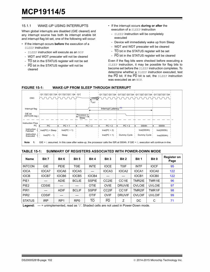
MCP19114/5
15.1.1 WAKE-UP USING INTERRUPTSWhen global interrupts are disabled (GIE cleared) andany interrupt source has both its interrupt enable bitand interrupt flag bit set, one of the following will occur:• If the interrupt occurs before the execution of a SLEEP instruction- SLEEP instruction will execute as an NOP- WDT and WDT prescaler will not be cleared- TO bit in the STATUS register will not be set- PD bit in the STATUS register will not be
cleared
DS20005281B-page 102
• If the interrupt occurs during or after the execution of a SLEEP instruction- SLEEP instruction will be completely
executed- Device will immediately wake up from Sleep- WDT and WDT prescaler will be cleared- TO bit in the STATUS register will be set- PD bit in the STATUS register will be cleared
Even if the flag bits were checked before executing aSLEEP instruction, it may be possible for flag bits tobecome set before the SLEEP instruction completes. Todetermine whether a SLEEP instruction executed, testthe PD bit. If the PD bit is set, the SLEEP instructionwas executed as an NOP.
FIGURE 15-1: WAKE-UP FROM SLEEP THROUGH INTERRUPT
TABLE 15-1: SUMMARY OF REGISTERS ASSOCIATED WITH POWER-DOWN MODE
Name Bit 7 Bit 6 Bit 5 Bit 4 Bit 3 Bit 2 Bit 1 Bit 0 Register on Page
INTCON GIE PEIE T0IE INTE IOCE T0IF INTF IOCF 95IOCA IOCA7 IOCA6 IOCA5 — IOCA3 IOCA2 IOCA1 IOCA0 122IOCB IOCB7 IOCB6 IOCB5 IOCB4 — — IOCB1 IOCB0 122PIE1 — ADIE BCLIE SSPIE CC2IE CC1IE TMR2IE TMR1IE 96PIE2 CDSIE — — OTIE OVIE DRUVIE OVLOIE UVLOIE 97PIR1 — ADIF BCLIF SSPIF CC2IF CC1IF TMR2IF TMR1IF 98PIR2 CDSIF — — OTIF OVIF DRUVIF OVLOIF UVLOIF 99
STATUS IRP RP1 RP0 TO PD Z DC C 71Legend: — = unimplemented, read as ‘0’. Shaded cells are not used in Power-Down mode.
Q1 Q2 Q3 Q4 Q1 Q2 Q3 Q4 Q1 Q1 Q2 Q3 Q4 Q1 Q2 Q3 Q4 Q1 Q2 Q3 Q4 Q1 Q2 Q3 Q4OSC
Interrupt flag
GIE bit(INTCON reg.)
Instruction FlowPC
InstructionFetchedInstructionExecuted
PC PC + 1 PC + 2
Inst(PC) = Sleep
Inst(PC - 1)
Inst(PC + 1)
Sleep
Processor inSleep
Inst(PC + 2)
Inst(PC + 1)
Inst(0004h) Inst(0005h)
Inst(0004h)Dummy Cycle
PC + 2 0004h 0005h
Dummy Cycle
TOST
PC + 2
Note 1: GIE = 1 assumed. In this case after wake-up, the processor calls the ISR at 0004h. If GIE = 0, execution will continue in-line.
Interrupt Latency (1)
2014-2015 Microchip Technology Inc.
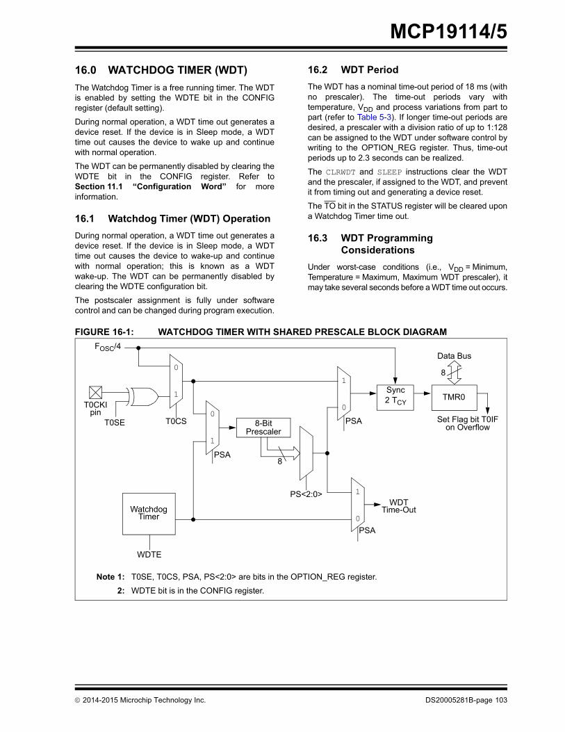
MCP19114/5
16.0 WATCHDOG TIMER (WDT)The Watchdog Timer is a free running timer. The WDTis enabled by setting the WDTE bit in the CONFIGregister (default setting).
During normal operation, a WDT time out generates adevice reset. If the device is in Sleep mode, a WDTtime out causes the device to wake up and continuewith normal operation.
The WDT can be permanently disabled by clearing theWDTE bit in the CONFIG register. Refer toSection 11.1 “Configuration Word” for moreinformation.
16.1 Watchdog Timer (WDT) OperationDuring normal operation, a WDT time out generates adevice reset. If the device is in Sleep mode, a WDTtime out causes the device to wake-up and continuewith normal operation; this is known as a WDTwake-up. The WDT can be permanently disabled byclearing the WDTE configuration bit.
The postscaler assignment is fully under softwarecontrol and can be changed during program execution.
2014-2015 Microchip Technology Inc.
16.2 WDT PeriodThe WDT has a nominal time-out period of 18 ms (withno prescaler). The time-out periods vary withtemperature, VDD and process variations from part topart (refer to Table 5-3). If longer time-out periods aredesired, a prescaler with a division ratio of up to 1:128can be assigned to the WDT under software control bywriting to the OPTION_REG register. Thus, time-outperiods up to 2.3 seconds can be realized.
The CLRWDT and SLEEP instructions clear the WDTand the prescaler, if assigned to the WDT, and preventit from timing out and generating a device reset.
The TO bit in the STATUS register will be cleared upona Watchdog Timer time out.
16.3 WDT Programming Considerations
Under worst-case conditions (i.e., VDD = Minimum,Temperature = Maximum, Maximum WDT prescaler), itmay take several seconds before a WDT time out occurs.
FIGURE 16-1: WATCHDOG TIMER WITH SHARED PRESCALE BLOCK DIAGRAM
T0CKI
T0SEpin
TMR0
WatchdogTimer
WDTTime-Out
PS<2:0>
Data Bus
Set Flag bit T0IFon Overflow
T0CS
Note 1: T0SE, T0CS, PSA, PS<2:0> are bits in the OPTION_REG register.
2: WDTE bit is in the CONFIG register.
0
1
0
1
0
1
8
8
8-BitPrescaler
0
1
FOSC/4
PSA
PSA
PSA
WDTE
Sync2 TCY
DS20005281B-page 103
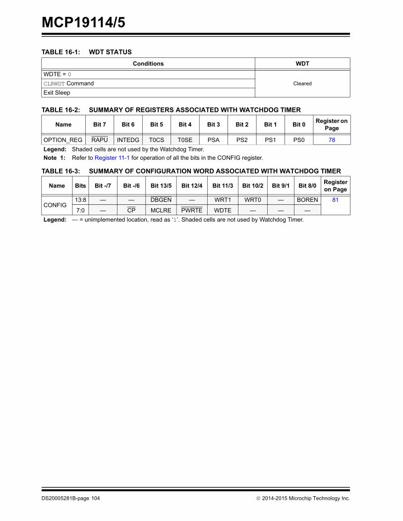
MCP19114/5
TABLE 16-1: WDT STATUSConditions WDT
WDTE = 0
ClearedCLRWDT CommandExit Sleep
TABLE 16-2: SUMMARY OF REGISTERS ASSOCIATED WITH WATCHDOG TIMER
Name Bit 7 Bit 6 Bit 5 Bit 4 Bit 3 Bit 2 Bit 1 Bit 0 Register on Page
OPTION_REG RAPU INTEDG T0CS T0SE PSA PS2 PS1 PS0 78Legend: Shaded cells are not used by the Watchdog Timer.Note 1: Refer to Register 11-1 for operation of all the bits in the CONFIG register.
TABLE 16-3: SUMMARY OF CONFIGURATION WORD ASSOCIATED WITH WATCHDOG TIMER
Name Bits Bit -/7 Bit -/6 Bit 13/5 Bit 12/4 Bit 11/3 Bit 10/2 Bit 9/1 Bit 8/0 Register on Page
CONFIG13:8 — — DBGEN — WRT1 WRT0 — BOREN 81
7:0 — CP MCLRE PWRTE WDTE — — —Legend: — = unimplemented location, read as ‘1’. Shaded cells are not used by Watchdog Timer.
DS20005281B-page 104 2014-2015 Microchip Technology Inc.

MCP19114/5
17.0 FLASH PROGRAM MEMORY CONTROL
The Flash program memory is readable and writableduring normal operation (full VIN range). This memory isnot directly mapped in the register file space. Instead, itis indirectly addressed through the Special FunctionRegisters (refer to Registers 17-1 to 17-5). There aresix SFRs used to read and write this memory:
• PMCON1• PMCON2• PMDATL• PMDATH• PMADRL• PMADRH
When interfacing the program memory block, thePMDATL and PMDATH registers form a two-byte wordwhich holds the 14-bit data for read/write, and thePMADRL and PMADRH registers form a two-byteword which holds the 13-bit address of the FLASHlocation being accessed. These devices have 4kwords of program Flash with an address range from0000h to 0FFFh.
The program memory allows single-word read and afour-word write. A four-word write automatically erasesthe row of the location and writes the new data (erasebefore write).
The write time is controlled by an on-chip timer. Thewrite/erase voltages are generated by an on-chipcharge pump rated to operate over the voltage rangeof the device for byte or word operations.
When the device is code-protected, the CPU maycontinue to read and write the Flash program memory.
Depending on the settings of the Flash ProgramMemory Enable (WRT<1:0>) bits, the device may ormay not be able to write certain blocks of the programmemory; however, reads of the program memory areallowed.
When the Flash Program Memory Code Protection(CP) bit is enabled, the program memory iscode-protected and the device programmer (ICSP)cannot access data or program memory.
2014-2015 Microchip Technology Inc.
17.1 PMADRH and PMADRL RegistersThe PMADRH and PMADRL registers can address upto a maximum of 4k words of program memory.
When selecting a program address value, the MostSignificant Byte (MSB) of the address is written to thePMADRH register and the Least Significant Byte(LSB) is written to the PMADRL register.
17.2 PMCON1 and PMCON2 RegistersThe PMCON1 register is the control register for thedata program memory accesses.
Control bits RD and WR initiate read and write,respectively. In software, these bits can only be set,not cleared. They are cleared in hardware atcompletion of the read or write operation. The inabilityto clear the WR bit in software prevents the accidentalpremature termination of a write operation.
The WREN bit, when set, will allow a write operation.On power-up, the WREN bit is clear.
The CALSEL bit allows the user to read locations intest memory in case there are calibration bits stored inthe calibration word locations that need to betransferred to SFR trim registers. The CALSEL bit isonly for reads. If a write operation is attempted withCALSEL = 1, no write will occur.
PMCON2 is not a physical register. Reading PMCON2will read all '0's. The PMCON2 register is usedexclusively in the flash memory write sequence.
DS20005281B-page 105
MCP19114/5
17.3 Flash Program Memory Control RegistersREGISTER 17-1: PMDATL: PROGRAM MEMORY DATA LOW BYTE REGISTERR/W-0 R/W-0 R/W-0 R/W-0 R/W-0 R/W-0 R/W-0 R/W-0PMDATL<7:0>
bit 7 bit 0
Legend:R = Readable bit W = Writable bit U = Unimplemented bit, read as ‘0’-n = Value at POR ‘1’ = Bit is set ‘0’ = Bit is cleared x = Bit is unknown
bit 7-0 PMDATL<7:0>: 8 Least Significant Data bits to Write or Read from Program Memory
REGISTER 17-2: PMADRL: PROGRAM MEMORY ADDRESS LOW BYTE REGISTER
R/W-0 R/W-0 R/W-0 R/W-0 R/W-0 R/W-0 R/W-0 R/W-0PMADRL<7:0>
bit 7 bit 0
Legend:R = Readable bit W = Writable bit U = Unimplemented bit, read as ‘0’-n = Value at POR ‘1’ = Bit is set ‘0’ = Bit is cleared x = Bit is unknown
bit 7-0 PMADRL<7:0>: 8 Least Significant Address bits for Program Memory Read/Write Operation
REGISTER 17-3: PMDATH: PROGRAM MEMORY DATA HIGH BYTE REGISTER
U-0 U-0 R/W-0 R/W-0 R/W-0 R/W-0 R/W-0 R/W-0— — PMDATH<5:0>
bit 7 bit 0
Legend:R = Readable bit W = Writable bit U = Unimplemented bit, read as ‘0’-n = Value at POR ‘1’ = Bit is set ‘0’ = Bit is cleared x = Bit is unknown
bit 7-6 Unimplemented: Read as ‘0’bit 5-0 PMDATH<5:0>: 6 Most Significant Data bits from Program Memory
DS20005281B-page 106 2014-2015 Microchip Technology Inc.
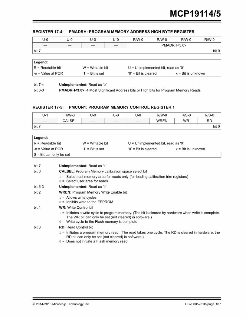
MCP19114/5
REGISTER 17-4: PMADRH: PROGRAM MEMORY ADDRESS HIGH BYTE REGISTER
U-0 U-0 U-0 U-0 R/W-0 R/W-0 R/W-0 R/W-0— — — — PMADRH<3:0>
bit 7 bit 0
Legend:R = Readable bit W = Writable bit U = Unimplemented bit, read as ‘0’-n = Value at POR ‘1’ = Bit is set ‘0’ = Bit is cleared x = Bit is unknown
bit 7-4 Unimplemented: Read as ‘0’bit 3-0 PMADRH<3:0>: 4 Most Significant Address bits or High bits for Program Memory Reads
REGISTER 17-5: PMCON1: PROGRAM MEMORY CONTROL REGISTER 1
U-1 R/W-0 U-0 U-0 U-0 R/W-0 R/S-0 R/S-0— CALSEL — — — WREN WR RD
bit 7 bit 0
Legend:R = Readable bit W = Writable bit U = Unimplemented bit, read as ‘0’-n = Value at POR ‘1’ = Bit is set ‘0’ = Bit is cleared x = Bit is unknownS = Bit can only be set
bit 7 Unimplemented: Read as '1'bit 6 CALSEL: Program Memory calibration space select bit
1 = Select test memory area for reads only (for loading calibration trim registers)0 = Select user area for reads
bit 5-3 Unimplemented: Read as '0'bit 2 WREN: Program Memory Write Enable bit
1 = Allows write cycles0 = Inhibits write to the EEPROM
bit 1 WR: Write Control bit1 = Initiates a write cycle to program memory. (The bit is cleared by hardware when write is complete.
The WR bit can only be set (not cleared) in software.)0 = Write cycle to the Flash memory is complete
bit 0 RD: Read Control bit1 = Initiates a program memory read. (The read takes one cycle. The RD is cleared in hardware; the
RD bit can only be set (not cleared) in software.)0 = Does not initiate a Flash memory read
2014-2015 Microchip Technology Inc. DS20005281B-page 107

MCP19114/5
17.3.1 READING THE FLASH PROGRAMMEMORYTo read a program memory location, the user mustwrite two bytes of the address to the PMADRL andPMADRH registers, and then set control bit RD (bit 0in the PMCON1register). Once the read control bit isset, the Program Memory Flash controller will use thesecond instruction cycle to read the data. This causesthe second instruction immediately following the BSFPMCON1,RD instruction to be ignored. The data isavailable, in the very next cycle, in the PMDATL andPMDATH registers; it can be read as two bytes in thefollowing instructions. PMDATL and PMDATHregisters will hold this value until another read or until itis written to by the user (during a write operation).
DS20005281B-page 108
EXAMPLE 17-1: FLASH PROGRAM READ
FIGURE 17-1: FLASH PROGRAM MEMORY READ CYCLE EXECUTION – NORMAL MODE
BANKSELPM_ADR; Change STATUS bits RP1:0 to select bank with PMADR
MOVLWMS_PROG_PM_ADDR;
MOVWFPMADRH; MS Byte of Program Address to read
MOVLWLS_PROG_PM_ADDR;
MOVWFPMADRL; LS Byte of Program Address to read
BANKSELPMCON1; Bank to containing PMCON1
BSF PMCON1, RD; EE Read
NOP ; First instruction after BSF PMCON1,RD executes normally
NOP ; Any instructions here are ignored as program
; memory is read in second cycle after BSF PMCON1,RD
;
BANKSELPMDATL; Bank to containing PMADRL
MOVFPMDATL, W; W = LS Byte of Program PMDATL
MOVFPMDATH, W; W = MS Byte of Program PMDATL
Q1 Q2 Q3 Q4 Q1 Q2 Q3 Q4 Q1 Q2 Q3 Q4 Q1 Q2 Q3 Q4 Q1 Q2 Q3 Q4 Q1 Q2 Q3 Q4
BSF PMCON1,RDExecuted here
INSTR (PC + 1)Executed here
NOPExecuted here
PC PC + 1 PMADRH,PMADRL PC+3 PC + 5Flash ADDR
RD bit
INSTR (PC) PMDATH,PMDATL INSTR (PC + 3)
PC + 3 PC + 4
INSTR (PC + 4)INSTR (PC + 1)
INSTR (PC - 1)Executed here
INSTR (PC + 3)Executed here
INSTR (PC + 4)Executed here
Flash DATA
PMDATHPMDATLRegister
EERHLT
2014-2015 Microchip Technology Inc.
MCP19114/5
17.3.2 WRITING TO THE FLASHPROGRAM MEMORYA word of the Flash program memory may only bewritten to if the word is in an unprotected segment ofmemory, as defined in Section 11.1 “ConfigurationWord” (bits <WRT1:0>).
Flash program memory must be written in four-wordblocks. Refer to Figures 17-2 and 17-3 for more details.A block consists of four words with sequentialaddresses, with a lower boundary defined by anaddress, where PMADRL<1:0> = 00. All block writes toprogram memory are done as 16-word erase byfour-word write operations. The write operation isedge-aligned and cannot occur across boundaries.
To write program data, the WREN bit must first beloaded into the buffer registers (refer to Figure 17-2).This is accomplished by first writing the destinationaddress to PMADRL and PMADRH and then writingthe data to PMDATL and PMDATH. After the addressand data have been set, the following sequence ofevents must be executed:
1. Write 55h, then AAh, to PMCON2 (Flashprogramming sequence).
2. Set the WR control bit in the PMCON1 register.
All four buffer register locations should be written towith correct data. If less than four words are beingwritten to in the block of four words, a read from theprogram memory location(s) not being written to mustbe performed. This takes the data from the programlocation(s) not being written and loads it into thePMDATL and PMDATH registers. Then the sequenceof events to transfer data to the buffer registers must beexecuted.
To transfer data from the buffer registers to the programmemory, the PMADRL and PMADRH must point to thelast location in the four-word block(PMADRL<1:0> = 11). Then the following sequence ofevents must be executed:
1. Write 55h, then AAh, to PMCON2 (Flashprogramming sequence).
2. Set control bit WR in the PMCON1 register tobegin the write operation.
Note: The write protect bits are used to protect theuser’s program from modification by theuser’s code. They have no effect whenprogramming is performed by ICSP. Thecode-protect bits, when programmed forcode protection, will prevent the programmemory from being written via the ICSPinterface.
2014-2015 Microchip Technology Inc.
The user must follow the same specific sequence toinitiate the write for each word in the program block,writing each program word in sequence (000, 001,010, 011). When the write is performed on the lastword (PMADRL<1:0> = 11), a block of sixteen words isautomatically erased and the content of the four-wordbuffer registers are written into the program memory.
After the BSF PMCON1,WR instruction, the processorrequires two cycles to set up the erase/write operation.The user must place two NOP instructions after the WRbit is set. Since data is being written to buffer registers,the writing of the first three words of the block appearsto occur immediately. The processor will halt internaloperations for the typical 4 ms only during the cycle inwhich the erase takes place (i.e., the last word of thesixteen-word block erase). This is not Sleep mode, asthe clocks and peripherals will continue to run. Afterthe four-word write cycle, the processor will resumeoperation with the third instruction after the PMCON1write instruction. The above sequence must berepeated for the higher 12 words.
Refer to Figure 17-2 for a block diagram of the bufferregisters and the control signals for test mode.
17.3.3 PROTECTION AGAINST SPURIOUS WRITE
There are conditions when the device should not writeto the program memory. To protect against spuriouswrites, various mechanisms have been built in. Onpower-up, WREN is cleared. Also, the Power-UpTimer (72 ms duration) prevents program memorywrites.
The write initiate sequence and the WREN bit helpprevent an accidental write during a power glitch orsoftware malfunction.
17.3.4 OPERATION DURING CODE PROTECT
When the device is code-protected, the CPU is able toread and write unscrambled data to the programmemory. The test mode access is disabled.
17.3.5 OPERATION DURING WRITE PROTECT
When the program memory is write-protected, theCPU can read and execute from the program memory.The portions of program memory that arewrite-protected cannot be modified by the CPU usingthe PMCON registers. The write protection has noeffect in ICSP mode.
Note: An erase is only initiated for the write of four words just after a row boundary; or PMCON1<WR> set with PMADRL<3:0> = xxxx0011.
DS20005281B-page 109

MCP19114/5
FIGURE 17-2: BLOCK WRITES TO 4K FLASH PROGRAM MEMORYFIGURE 17-3: FLASH PROGRAM MEMORY LONG WRITE CYCLE EXECUTION
14 14 14 14
Program Memory
Buffer Register
PMADRL<1:0> = 00
Buffer Register
PMADRL<1:0> = 01
Buffer Register
PMADRL<1:0> = 10
Buffer Register
PMADRL<1:0> = 11
PMDATLPMDATH
7 5 0 7 0
6 8
First word of blockto be written
If at new rowsixteen words ofFlash are erased,then four buffers aretransferred to Flashautomatically afterthis word is written
Q1 Q2 Q3 Q4 Q1 Q2 Q3 Q4 Q1 Q2 Q3 Q4 Q1 Q4 Q1 Q2 Q3 Q4 Q1 Q2 Q3 Q4 Q1 Q2 Q3 Q4
BSF PMCON1,WRExecuted here
INSTR (PC + 1)Executed here
PC + 1Flash
INSTR PMDATH, PMDATL INSTR (PC+3)INSTR
NOPExecuted here
Flash
Flash
PMWHLT
WR bit
Processor halted EE Write Time
PMADRH, PMADRL PC + 3 PC + 4
INSTR (PC + 3)Executed here
ADDR
DATA
MemoryLocation
ignoredread
PC + 2
INSTR (PC+2)
(INSTR (PC + 2)NOP
Executed here
(PC) (PC + 1)
DS200052
81B-page 110 2014-201 5 Microchip Technology Inc.
MCP19114/5
18.0 I/O PORTSIn general, when a peripheral is enabled, that pin maynot be used as a general-purpose I/O pin.
Each port has the registers for its operation. Theseregisters are:
• TRISGPx registers (data direction register)• PORTGPx registers (read the levels on the pins of
the device)
Some ports may have one or more of the followingadditional registers. These registers are:
• ANSELx (analog select)• WPUGPx (weak pull-up)
Ports with analog functions also have an ANSELxregister, which can disable the digital input and savepower. A simplified model of a generic I/O port, withoutthe interfaces to other peripherals, is shown inFigure 18-1.
FIGURE 18-1: GENERIC I/O PORTGPX OPERATION
EXAMPLE 18-1: INITIALIZING PORTGPA
QD
CK
Write LATx
Data Register
Read PORTGPx
Write PORTGPx
TRISGPxRead LATx
Data Bus
To peripherals
ANSELx
VDD
VSS
I/O pin
; This code example illustrates
; initializing the PORTGPA register. The
; other ports are initialized in the same
; manner.
BANKSEL PORTGPA;
CLRF PORTGPA;Init PORTA
BANKSEL ANSELA;
CLRF ANSELA;digital I/O
BANKSEL TRISGPA;
MOVLW B'00011111';Set GPA<3:0> as
;inputs
MOVWF TRISGPA;and set GPA<7:5> as
;outputs
2014-2015 Microchip Technology Inc.
18.1 PORTGPA and TRISGPA RegistersPORTGPA is an 8-bit wide, bidirectional port consistingof five CMOS I/Os, one open-drain I/O and oneopen-drain input-only pin (GPA4 is not available). Thecorresponding data direction register is TRISGPA.Setting a TRISGPA bit to 1 will make the correspondingPORTGPA pin an input (i.e., disable the output driver).Clearing a TRISGPA bit set to 0 will make thecorresponding PORTGPA pin an output (i.e., enablesoutput driver). The exception is GPA5, which is inputonly and its TRISGPA bit will always read as ‘1’.Example 18-1 shows how to initialize an I/O port.
Reading the PORTGPA register reads the status of thepins, whereas writing to it will write to the PORT latch.All write operations are read-modify-write operations.
The TRISGPA register controls the PORTGPA pinoutput drivers, even when they are being used asanalog inputs. The user must ensure the bits in theTRISGPA register are maintained set when using themas analog inputs. I/O pins configured as analog inputalways read ‘0’. If the pin is configured for a digitaloutput (either port or alternate function), the TRISGPAbit must be cleared in order for the pin to drive thesignal, and a read will reflect the state of the pin.
18.1.1 INTERRUPT-ON-CHANGEEach PORTGPA pin is individually configurable as aninterrupt-on-change pin. Control bits IOCB<7:4> andIOCB<2:0> enable or disable the interrupt function foreach pin. The interrupt-on-change feature is disabledon a Power-On Reset. Reference Section 19.0“Interrupt-On-Change” for more information.
18.1.2 WEAK PULL-UPSPORTGPA <3:0> and PORTGPA5 have an internal weakpull-up. PORTGPA<7:6> do not have internal weakpull-ups. Individual control bits can enable or disable theinternal weak pull-ups (refer to Register 18-3). The weakpull-up is automatically turned off when the port pin isconfigured as an output, an alternative function or on aPower-On Reset setting the RAPU bit in theOPTION_REG register. The weak pull-up on GPA5 isenabled when configured as MCLR pin by setting bit 5 inthe CONFIG register, and disabled when GPA5 is an I/O.There is no software control of the MCLR pull-up.
DS20005281B-page 111

MCP19114/5
18.1.3 ANSELA REGISTERThe ANSELA register is used to configure the inputmode of an I/O pin to analog. Setting the appropriateANSELA bit high will cause all digital reads on the pinto be read as ‘0’ and allow analog functions on the pinto operate correctly.The state of the ANSELA bits has no effect on digitaloutput functions. A pin with TRISGPA cleared andANSELx set will still operate as a digital output, but theinput mode will be analog. This can cause unexpectedbehavior when executing read-modify-writeinstructions on the affected port.
18.1.4 PORTGPA FUNCTIONS AND OUTPUT PRIORITIES
Each PORTGPA pin is multiplexed with other functions.The pins, their combined functions and their outputpriorities are shown in Table 18-1. For additionalinformation, refer to the appropriate section in this datasheet.
Pin GPA7 in the PORTGPA register is a true open-drainpin with no connection back to VDD.
When multiple outputs are enabled, the actual pincontrol goes to the peripheral with the highest priority.
Analog input functions, such as ADC, are not shown inthe priority lists. These inputs are active when the I/Opin is set for Analog mode using the ANSELA register.Digital output functions may control the pin when it is inAnalog mode with the priority shown in Table 18-1.
Note: The ANSELA bits default to the Analogmode after Reset. To use any pins asdigital general-purpose or peripheralinputs, the corresponding ANSEL bitsmust be initialized to ‘0’ by the user’ssoftware.
DS20005281B-page 112
TABLE 18-1: PORTGPA OUTPUT PRIORITY
Pin Name Function Priority(1)
GPA0 GPA0TEST_OUT
GPA1 GPA1CLKPIN
GPA2 GPA2T0CKIINT
GPA3 GPA3GPA5 GPA5 (open-drain, input only)
MCLRTEST_EN
GPA6 GPA6CCDICSPDAT
GPA7 GPA7 (open-drain output, ST input)SCL
Note 1: Output function priority listed from lowest to highest.
2014-2015 Microchip Technology Inc.
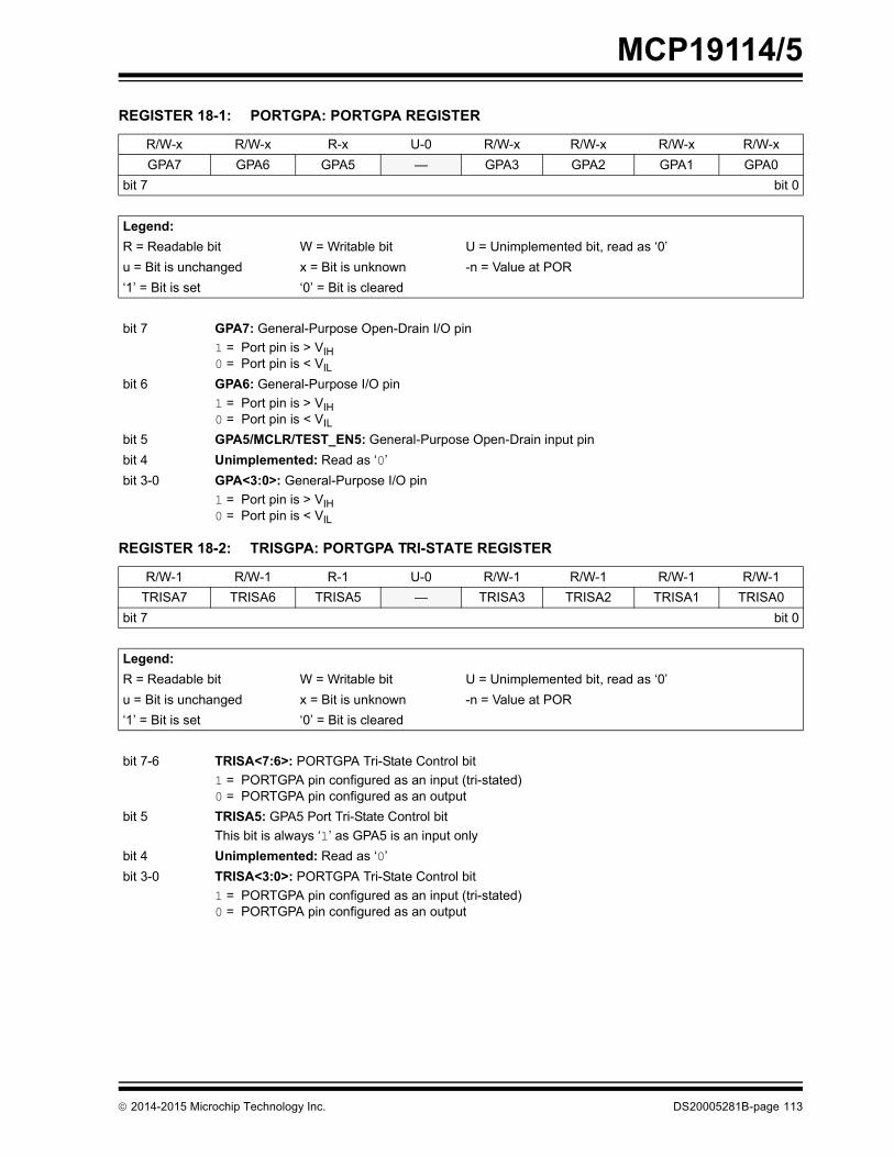
MCP19114/5
REGISTER 18-1: PORTGPA: PORTGPA REGISTER
R/W-x R/W-x R-x U-0 R/W-x R/W-x R/W-x R/W-xGPA7 GPA6 GPA5 — GPA3 GPA2 GPA1 GPA0
bit 7 bit 0
Legend:R = Readable bit W = Writable bit U = Unimplemented bit, read as ‘0’u = Bit is unchanged x = Bit is unknown -n = Value at POR‘1’ = Bit is set ‘0’ = Bit is cleared
bit 7 GPA7: General-Purpose Open-Drain I/O pin1 = Port pin is > VIH0 = Port pin is < VIL
bit 6 GPA6: General-Purpose I/O pin1 = Port pin is > VIH0 = Port pin is < VIL
bit 5 GPA5/MCLR/TEST_EN5: General-Purpose Open-Drain input pinbit 4 Unimplemented: Read as ‘0’bit 3-0 GPA<3:0>: General-Purpose I/O pin
1 = Port pin is > VIH0 = Port pin is < VIL
REGISTER 18-2: TRISGPA: PORTGPA TRI-STA
2014-2015 Microchip Technology Inc.
REGISTER
TER/W-1 R/W-1 R-1 U-0 R/W-1 R/W-1 R/W-1 R/W-1TRISA7 TRISA6 TRISA5 — TRISA3 TRISA2 TRISA1 TRISA0
bit 7 bit 0
Legend:R = Readable bit W = Writable bit U = Unimplemented bit, read as ‘0’u = Bit is unchanged x = Bit is unknown -n = Value at POR‘1’ = Bit is set ‘0’ = Bit is cleared
bit 7-6 TRISA<7:6>: PORTGPA Tri-State Control bit1 = PORTGPA pin configured as an input (tri-stated)0 = PORTGPA pin configured as an output
bit 5 TRISA5: GPA5 Port Tri-State Control bitThis bit is always ‘1’ as GPA5 is an input only
bit 4 Unimplemented: Read as ‘0’bit 3-0 TRISA<3:0>: PORTGPA Tri-State Control bit
1 = PORTGPA pin configured as an input (tri-stated)0 = PORTGPA pin configured as an output
DS20005281B-page 113

MCP19114/5
REGISTER 18-3: WPUGPA: WEAK PULL-UP PORTGPA REGISTER
U-0 U-0 R/W-1 U-0 R/W-1 R/W-1 R/W-1 R/W-1— — WPUA5 — WPUA3 WPUA2 WPUA1 WPUA0
bit 7 bit 0
Legend:R = Readable bit W = Writable bit U = Unimplemented bit, read as ‘0’u = Bit is unchanged x = Bit is unknown -n = Value at POR‘1’ = Bit is set ‘0’ = Bit is cleared
bit 7-6 Unimplemented: Read as ‘0’bit 5 WPUA5: Weak Pull-Up Register bit
1 = Pull-up enabled0 = Pull-up disabled
bit 4 Unimplemented: Read as ‘0’bit 3-0 WPUA<3:0>: Weak Pull-Up Register bit
1 = Pull-up enabled0 = Pull-up disabled
Note 1: The weak pull-up device is enabled only when the global RAPU bit is enabled, the pin is in input mode (TRISGPA = 1) and the individual WPUA bit is enabled (WPUA = 1), and the pin is not configured as an analog input.
2: GPA5 weak pull-up is also enabled when the pin is configured as MCLR in the CONFIG register.
REGISTER 18-4: ANSELA: ANALOG SELECT GPA REGISTER
U-0 U-0 U-0 U-0 R/W-1 R/W-1 R/W-1 R/W-1— — — — ANSA3 ANSA2 ANSA1 ANSA0
bit 7 bit 0
Legend:R = Readable bit W = Writable bit U = Unimplemented bit, read as ‘0’u = Bit is unchanged x = Bit is unknown -n = Value at POR‘1’ = Bit is set ‘0’ = Bit is cleared
bit 7-4 Unimplemented: Read as ‘0’bit 3-0 ANSA<3:0>: Analog Select GPA Register bit
1 = Analog input. Pin is assigned as analog input.(1)
0 = Digital I/O. Pin is assigned to port or special function.
Note 1: Setting a pin to an analog input automatically disables the digital input circuitry, weak pull-ups and interrupt-on-change if available. The corresponding TRISA bit must be set to Input mode in order to allow external control of the voltage on the pin.
DS20005281B-page 114 2014-2015 Microchip Technology Inc.

MCP19114/5
TABLE 18-2: SUMMARY OF REGISTERS ASSOCIATED WITH PORTGPA
Name Bit 7 Bit 6 Bit 5 Bit 4 Bit 3 Bit 2 Bit 1 Bit 0 Register on Page
ANSELA — — — — ANSA3 ANSA2 ANSA1 ANSA0 114
OPTION_REG RAPU INTEDG T0CS T0SE PSA PS2 PS1 PS0 78
PORTGPA GPA7 GPA6 GPA5 — GPA3 GPA2 GPA1 GPA0 113TRISGPA TRISA7 TRISA6 TRISA5 — TRISA3 TRISA2 TRISA1 TRISA0 113WPUGPA — — WPUA5 — WPUA3 WPUA2 WPUA1 WPUA0 114Legend: — = unimplemented locations read as ‘0’. Shaded cells are not used by PORTGPA.
2014-2015 Microchip Technology Inc. DS20005281B-page 115
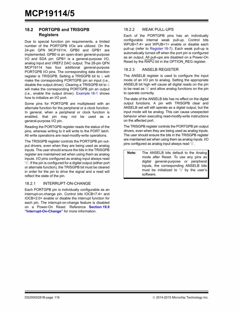
MCP19114/5
18.2 PORTGPB and TRISGPBRegistersDue to special function pin requirements, a limitednumber of the PORTGPB I/Os are utilized. On the24-pin QFN MCP19114, GPB0 and GPB1 areimplemented. GPB0 is an open-drain general-purposeI/O and SDA pin. GPB1 is a general-purpose I/O,analog input and VREF2 DAC output. The 28-pin QFNMCP19114 has four additional general-purposePORTGPB I/O pins. The corresponding data directionregister is TRISGPB. Setting a TRISGPB bit to 1 willmake the corresponding PORTGPB pin an input (i.e.,disable the output driver). Clearing a TRISGPB bit to 0will make the corresponding PORTGPB pin an output(i.e., enable the output driver). Example 18-1 showshow to initialize an I/O port.
Some pins for PORTGPB are multiplexed with analternate function for the peripheral or a clock function.In general, when a peripheral or clock function isenabled, that pin may not be used as ageneral-purpose I/O pin.
Reading the PORTGPB register reads the status of thepins, whereas writing to it will write to the PORT latch.All write operations are read-modify-write operations.
The TRISGPB register controls the PORTGPB pin out-put drivers, even when they are being used as analoginputs. The user should ensure the bits in the TRISGPBregister are maintained set when using them as analoginputs. I/O pins configured as analog input always read‘0’. If the pin is configured for a digital output (either portor alternate function), the TRISGPB bit must be clearedin order for the pin to drive the signal and a read willreflect the state of the pin.
18.2.1 INTERRUPT-ON-CHANGEEach PORTGPB pin is individually configurable as aninterrupt-on-change pin. Control bits IOCB<7:4> andIOCB<2:0> enable or disable the interrupt function foreach pin. The interrupt-on-change feature is disabledon a Power-On Reset. Reference Section 19.0“Interrupt-On-Change” for more information.
DS20005281B-page 116
18.2.2 WEAK PULL-UPSEach of the PORTGPB pins has an individuallyconfigurable internal weak pull-up. Control bitsWPUB<7:4> and WPUB<1> enable or disable eachpull-up (refer to Register 18-7). Each weak pull-up isautomatically turned off when the port pin is configuredas an output. All pull-ups are disabled on a Power-OnReset by the RAPU bit in the OPTION_REG register.
18.2.3 ANSELB REGISTERThe ANSELB register is used to configure the inputmode of an I/O pin to analog. Setting the appropriateANSELB bit high will cause all digital reads on the pinto be read as ‘0’ and allow analog functions on the pinto operate correctly.
The state of the ANSELB bits has no effect on the digitaloutput functions. A pin with TRISGPB clear andANSELB set will still operate as a digital output, but theinput mode will be analog. This can cause unexpectedbehavior when executing read-modify-write instructionson the affected port.
The TRISGPB register controls the PORTGPB pin outputdrivers, even when they are being used as analog inputs.The user should ensure the bits in the TRISGPB registerare maintained set when using them as analog inputs. I/Opins configured as analog input always read ‘0’.
Note: The ANSELB bits default to the Analogmode after Reset. To use any pins asdigital general-purpose or peripheralinputs, the corresponding ANSELB bitsmust be initialized to ‘0’ by the user’ssoftware.
2014-2015 Microchip Technology Inc.
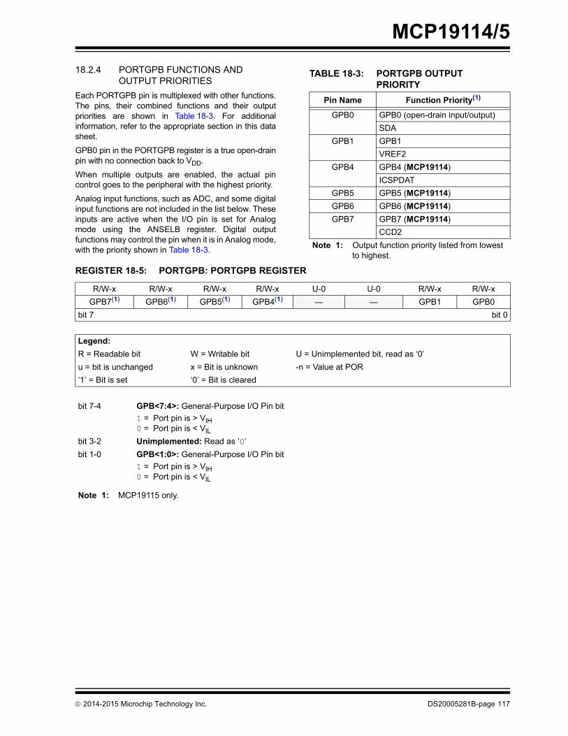
MCP19114/5
18.2.4 PORTGPB FUNCTIONS ANDOUTPUT PRIORITIESEach PORTGPB pin is multiplexed with other functions.The pins, their combined functions and their outputpriorities are shown in Table 18-3. For additionalinformation, refer to the appropriate section in this datasheet.
GPB0 pin in the PORTGPB register is a true open-drainpin with no connection back to VDD.
When multiple outputs are enabled, the actual pincontrol goes to the peripheral with the highest priority.
Analog input functions, such as ADC, and some digitalinput functions are not included in the list below. Theseinputs are active when the I/O pin is set for Analogmode using the ANSELB register. Digital outputfunctions may control the pin when it is in Analog mode,with the priority shown in Table 18-3.
2014-2015 Microchip Technology Inc.
TABLE 18-3: PORTGPB OUTPUT PRIORITY
Pin Name Function Priority(1)
GPB0 GPB0 (open-drain input/output)SDA
GPB1 GPB1VREF2
GPB4 GPB4 (MCP19114)ICSPDAT
GPB5 GPB5 (MCP19114)GPB6 GPB6 (MCP19114)GPB7 GPB7 (MCP19114)
CCD2Note 1: Output function priority listed from lowest
to highest.
REGISTER 18-5: PORTGPB: PORTGPB REGISTER
R/W-x R/W-x R/W-x R/W-x U-0 U-0 R/W-x R/W-xGPB7(1) GPB6(1) GPB5(1) GPB4(1) — — GPB1 GPB0
bit 7 bit 0
Legend:R = Readable bit W = Writable bit U = Unimplemented bit, read as ‘0’u = bit is unchanged x = Bit is unknown -n = Value at POR‘1’ = Bit is set ‘0’ = Bit is cleared
bit 7-4 GPB<7:4>: General-Purpose I/O Pin bit1 = Port pin is > VIH0 = Port pin is < VIL
bit 3-2 Unimplemented: Read as ‘0’bit 1-0 GPB<1:0>: General-Purpose I/O Pin bit
1 = Port pin is > VIH0 = Port pin is < VIL
Note 1: MCP19115 only.
DS20005281B-page 117
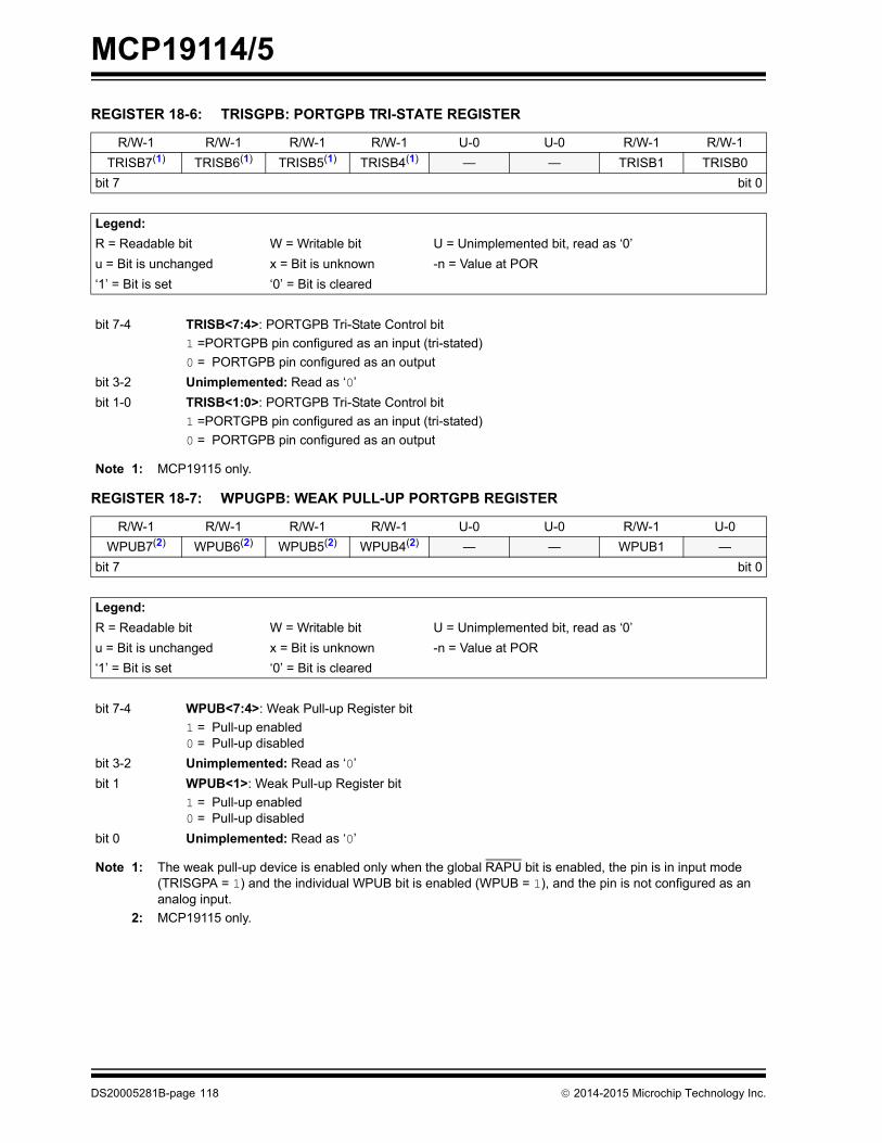
MCP19114/5
REGISTER 18-6: TRISGPB: PORTGPB TRI-STATE REGISTER
R/W-1 R/W-1 R/W-1 R/W-1 U-0 U-0 R/W-1 R/W-1TRISB7(1) TRISB6(1) TRISB5(1) TRISB4(1) — — TRISB1 TRISB0
bit 7 bit 0
Legend:R = Readable bit W = Writable bit U = Unimplemented bit, read as ‘0’u = Bit is unchanged x = Bit is unknown -n = Value at POR‘1’ = Bit is set ‘0’ = Bit is cleared
bit 7-4 TRISB<7:4>: PORTGPB Tri-State Control bit1 =PORTGPB pin configured as an input (tri-stated)0 = PORTGPB pin configured as an output
bit 3-2 Unimplemented: Read as ‘0’bit 1-0 TRISB<1:0>: PORTGPB Tri-State Control bit
1 =PORTGPB pin configured as an input (tri-stated)0 = PORTGPB pin configured as an output
Note 1: MCP19115 only.
REGISTER 18-7: WPUGPB: WEAK PULL-UP PORTGPB REGISTER
R/W-1 R/W-1 R/W-1 R/W-1 U-0 U-0 R/W-1 U-0WPUB7(2) WPUB6(2) WPUB5(2) WPUB4(2) — — WPUB1 —
bit 7 bit 0
Legend:R = Readable bit W = Writable bit U = Unimplemented bit, read as ‘0’u = Bit is unchanged x = Bit is unknown -n = Value at POR‘1’ = Bit is set ‘0’ = Bit is cleared
bit 7-4 WPUB<7:4>: Weak Pull-up Register bit1 = Pull-up enabled0 = Pull-up disabled
bit 3-2 Unimplemented: Read as ‘0’bit 1 WPUB<1>: Weak Pull-up Register bit
1 = Pull-up enabled0 = Pull-up disabled
bit 0 Unimplemented: Read as ‘0’
Note 1: The weak pull-up device is enabled only when the global RAPU bit is enabled, the pin is in input mode (TRISGPA = 1) and the individual WPUB bit is enabled (WPUB = 1), and the pin is not configured as an analog input.
2: MCP19115 only.
DS20005281B-page 118 2014-2015 Microchip Technology Inc.

MCP19114/5
REGISTER 18-8: ANSELB: ANALOG SELECT GPB REGISTER
U-0 R/W-1 R/W-1 R/W-1 U-0 U-0 R/W-1 U-0— ANSB6(1) ANSB5(1) ANSB4(1) — — ANSB1 —
bit 7 bit 0
Legend:R = Readable bit W = Writable bit U = Unimplemented bit, read as ‘0’u = Bit is unchanged x = Bit is unknown -n = Value at POR‘1’ = Bit is set ‘0’ = Bit is cleared
bit 7 Unimplemented: Read as ‘0’bit 6-4 ANSB<6:4>: Analog Select GPB Register bit
1 = Analog input. Pin is assigned as analog input(1).0 = Digital I/O. Pin is assigned to port or special function.
bit 3-2 Unimplemented: Read as ‘0’bit 1 ANSB1: Analog Select GPB Register bit
1 = Analog input. Pin is assigned as analog input(1).0 = Digital I/O. Pin is assigned to port or special function.
bit 0 Unimplemented: Read as ‘0’
Note 1: MCP19115 only.2: Setting a pin to an analog input automatically disables the digital input circuitry, weak pull-ups and
interrupt-on-change if available. The corresponding TRIS bit must be set to Input mode in order to allow external control of the voltage on the pin.
TABLE 18-4: SUMMARY OF REGISTERS ASSOCIATED WITH PORTGPB
Name Bit 7 Bit 6 Bit 5 Bit 4 Bit 3 Bit 2 Bit 1 Bit 0 Register on Page
ANSELB — ANSB6(1) ANSB5(1) ANSB4(1) — — ANSB1 — 119
OPTION_REG RAPU INTEDG T0CS T0SE PSA PS2 PS1 PS0 78PORTGPB GPB7(1) GPB6(1) GPB5(1) GPB4(1) — — GPB1 GPB0 117TRISGPB TRISB7(1) TRISB6(1) TRISB5(1) TRISB4(1) — — TRISB1 TRISB0 118WPUGPB WPUB7(1) WPUB6(1) WPUB5(1) WPUB4(1) — — WPUB1 — 118Legend: — = unimplemented locations, read as ‘0’. Shaded cells are not used by the PORTGPB register.Note 1: MCP19115 only.
2014-2015 Microchip Technology Inc. DS20005281B-page 119

MCP19114/5
NOTES:DS20005281B-page 120
2014-2015 Microchip Technology Inc.
MCP19114/5
19.0 INTERRUPT-ON-CHANGEEach PORTGPA and PORTGPB pin is individuallyconfigurable as an interrupt-on-change pin. Control bitsIOCA and IOCB enable or disable the interrupt functionfor each pin. Refer to Registers 19-1 and 19-2. Theinterrupt-on-change is disabled on a Power-On Reset.
The interrupt-on-change on GPA5 is disabled whenconfigured as MCLR pin in the CONFIG register.
For enabled interrupt-on-change pins, the values arecompared with the old value latched on the last read ofPORTGPA or PORTGPB. The mismatched outputs ofthe last read of all the PORTGPA and PORTGPB pinsare OR’ed together to set the Interrupt-on-ChangeInterrupt Flag (IOCF) bit in the INTCON register.
19.1 Enabling the ModuleTo allow individual port pins to generate an interrupt, theIOCE bit in the INTCON register must be set. If the IOCEbit is disabled, the edge detection on the pin will stilloccur, but an interrupt will not be generated.
19.2 Individual Pin ConfigurationTo enable a pin to detect an interrupt-on-change, theassociated IOCAx or IOCBx bit in the IOCA or IOCBregisters is set.
19.3 Clearing Interrupt FlagsThe user, in the Interrupt Service Routine, clears theinterrupt by:
a) Any read of PORTGPA or PORTGPB ANDClear flag bit IOCF. This will end the mismatchcondition.
OR
b) Any write of PORTGPA or PORTGPB ANDClear flag bit IOCF will end the mismatchcondition.
A mismatch condition will continue to set flag bit IOCF.Reading PORTGPA or PORTGPB will end themismatch condition and allow flag bit IOCF to becleared. The latch holding the last read value is notaffected by a MCLR Reset. After this Reset, the IOCFflag will continue to be set if a mismatch is present.
19.4 Operation in SleepThe interrupt-on-change interrupt sequence will wakethe device from Sleep mode, if the IOCE bit is set.
Note: If a change on the I/O pin should occurwhen any PORTGPA or PORTGPBoperation is being executed, the IOCFinterrupt flag may not get set.
2014-2015 Microchip Technology Inc.
DS20005281B-page 121
MCP19114/5
19.5 Interrupt-On-Change RegistersREGISTER 19-1: IOCA: INTERRUPT-ON-CHANGE PORTGPA REGISTER
R/W-0 R/W-0 R/W-0 U-0 R/W-0 R/W-0 R/W-0 R/W-0IOCA7 IOCA6 IOCA5 — IOCA3 IOCA2 IOCA1 IOCA0
bit 7 bit 0
Legend:R = Readable bit W = Writable bit U = Unimplemented bit, read as ‘0’u = Bit is unchanged x = Bit is unknown -n = Value at POR‘1’ = Bit is set ‘0’ = Bit is cleared
bit 7-6 IOCA<7:6>: Interrupt-on-Change PORTGPA register bits1 = Interrupt-on-change enabled on the pin.0 = Interrupt-on-change disabled on the pin.
bit 5 IOCA<5>: Interrupt-on-Change PORTGPA register bits(1)
1 = Interrupt-on-change enabled on the pin.0 = Interrupt-on-change disabled on the pin.
bit 4 Unimplemented: Read as ‘0’bit 3-0 IOCA<3:0>: Interrupt-on-Change PORTGPA register bits
1 = Interrupt-on-change enabled on the pin.0 = Interrupt-on-change disabled on the pin.
Note 1: The Interrupt-on-Change on GPA5 is disabled if GPA5 is configured as MCLR.
REGISTER 19-2: IOCB: INTERRUPT-ON-CHANGE PORTGPB REGISTER
R/W-0 R/W-0 R/W-0 R/W-0 U-0 U-0 R/W-0 R/W-0IOCB7(1) IOCB6(1) IOCB5(1) IOCB4(1) — — IOCB1 IOCB0
bit 7 bit 0
Legend:R = Readable bit W = Writable bit U = Unimplemented bit, read as ‘0’u = Bit is unchanged x = Bit is unknown -n = Value at POR‘1’ = Bit is set ‘0’ = Bit is cleared
bit 7-4 IOCB<7:4>: Interrupt-on-Change PORTGPB register bits1 = Interrupt-on-change enabled on the pin.0 = Interrupt-on-change disabled on the pin.
bit 3-2 Unimplemented: Read as ‘0’bit 1-0 IOCB<1:0>: Interrupt-on-Change PORTGPB register bits
1 = Interrupt-on-change enabled on the pin.0 = Interrupt-on-change disabled on the pin.
Note 1: MCP19115 only.
DS20005281B-page 122 2014-2015 Microchip Technology Inc.

MCP19114/5
TABLE 19-1: SUMMARY OF REGISTERS ASSOCIATED WITH INTERRUPT-ON-CHANGE
Name Bit 7 Bit 6 Bit 5 Bit 4 Bit 3 Bit 2 Bit 1 Bit 0 Register on Page
ANSELA — — — — ANSA3 ANSA2 ANSA1 ANSA0 114ANSELB — ANSB6(1) ANSB5(1) ANSB4(1) — — ANSB1 — 119INTCON GIE PEIE T0IE INTE IOCE T0IF INTF IOCF 95IOCA IOCA7 IOCA6 IOCA5 — IOCA3 IOCA2 IOCA1 IOCA0 122IOCB IOCB7(1) IOCB6(1) IOCB5(1) IOCB4(1) — — IOCB1 IOCB0 122TRISGPA TRISA7 TRISA6 TRISA5 — TRISA3 TRISA2 TRISA1 TRISA0 113TRISGPB TRISB7(1) TRISB6(1) TRISB5(1) TRISB4(1) — — TRISB1 TRISB0 118Legend: — = unimplemented locations, read as ‘0’. Shaded cells are not used by interrupt-on-change.Note 1: MCP19115 only.
2014-2015 Microchip Technology Inc. DS20005281B-page 123

MCP19114/5
NOTES:DS20005281B-page 124
2014-2015 Microchip Technology Inc.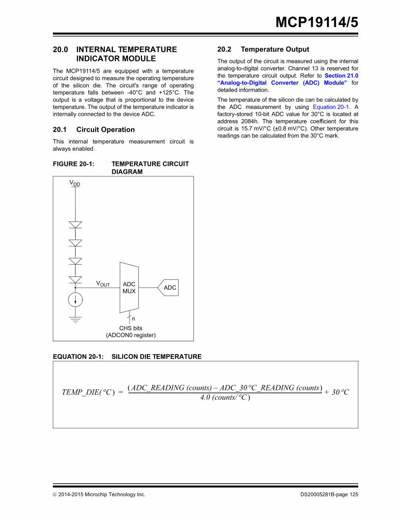
MCP19114/5
20.0 INTERNAL TEMPERATURE INDICATOR MODULE
The MCP19114/5 are equipped with a temperaturecircuit designed to measure the operating temperatureof the silicon die. The circuit's range of operatingtemperature falls between -40°C and +125°C. Theoutput is a voltage that is proportional to the devicetemperature. The output of the temperature indicator isinternally connected to the device ADC.
20.1 Circuit OperationThis internal temperature measurement circuit isalways enabled.
FIGURE 20-1: TEMPERATURE CIRCUIT DIAGRAM
ADCMUX
VDD
ADC
CHS bits(ADCON0 register)
n
VOUT
2014-2015 Microchip Technology Inc.
20.2 Temperature OutputThe output of the circuit is measured using the internalanalog-to-digital converter. Channel 13 is reserved forthe temperature circuit output. Refer to Section 21.0“Analog-to-Digital Converter (ADC) Module” fordetailed information.
The temperature of the silicon die can be calculated bythe ADC measurement by using Equation 20-1. Afactory-stored 10-bit ADC value for 30°C is located ataddress 2084h. The temperature coefficient for thiscircuit is 15.7 mV/°C (±0.8 mV/°C). Other temperaturereadings can be calculated from the 30°C mark.
EQUATION 20-1: SILICON DIE TEMPERATURE
TEMP_DIE(C ADC_READING (counts) ADC_30C_READING (counts– 4.0 (counts/C
----------------------------------------------------------------------------------------------------------------------------------------------------- 30C+=
DS20005281B-page 125

MCP19114/5
NOTES:DS20005281B-page 126
2014-2015 Microchip Technology Inc.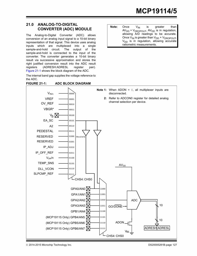
MCP19114/5
21.0 ANALOG-TO-DIGITAL CONVERTER (ADC) MODULE
The Analog-to-Digital Converter (ADC) allowsconversion of an analog input signal to a 10-bit binaryrepresentation of that signal. This device uses analoginputs which are multiplexed into a singlesample-and-hold circuit. The output of thesample-and-hold is connected to the input of theconverter. The converter generates a 10-bit binaryresult via successive approximation and stores theright justified conversion result into the ADC resultregisters (ADRESH:ADRESL register pair).Figure 21-1 shows the block diagram of the ADC.
The internal band gap supplies the voltage reference tothe ADC.
2014-2015 Microchip Technology Inc.
Note: Once VIN is greater thanAVDD + VDROPOUT, AVDD is in regulation,allowing A/D readings to be accurate.Once VIN is greater than VDD + VDROPOUT,VDD is in regulation, allowing accurateratiometric measurements.
FIGURE 21-1: ADC BLOCK DIAGRAM
GPA0/AN0
VREF
IP_ADJ
VBGR*
EA_SC
OV_REF
VS
CHS4: CHS0
ADC
ADON
GO/DONE
ADRESH ADRESL
10
10
VSS
A2
RESERVED
IP_OFF_REF
VIN/n
GPA1/AN1
GPA2/AN2
GPA3/AN3
GPB1/AN4
(MCP19115 Only) GPB4/AN5
(MCP19115 Only) GPB5/AN6
(MCP19115 Only) GPB6/AN7
CHS4: CHS0
VDR/n
TEMP_SNS
PEDESTAL
DLL_VCONSLPCMP_REF
AVDD
00000
00001
00010
00011
00100
00101
00110
00111
01000
01001
01010
01011
01100
01101
01110
01111
11000
11001
11010
11011
11100
11101
11110
11111
TRI-STATE
RESERVED
Note 1: When ADON = 0, all multiplexer inputs aredisconnected.
2: Refer to ADCON0 register for detailed analogchannel selection per device.
DS20005281B-page 127

MCP19114/5
21.1 ADC Configuration When configuring and using the ADC, the followingfunctions must be considered:• Port configuration• Channel selection• ADC conversion clock source• Interrupt control• Result formatting
21.1.1 PORT CONFIGURATIONThe ADC is used to convert analog signals into acorresponding digital representation. When convertinganalog signals, the I/O pin should be configured foranalog by setting the associated TRIS and ANSEL bits.Refer to Section 18.0 “I/O Ports” for moreinformation.
21.1.2 CHANNEL SELECTIONThere are up to 21 channel selections available for theMCP19114 and 24 channels for the MCP19115:
• AN<4:0> pins• AN<7:5> pins (MCP19115 Only)• VIN: 1/15.53 of the input voltage (VIN)• VREF: voltage reference for regulation set point• OV_REF: reference for OV comparator• VBGR: band gap reference• VS: voltage proportional to VOUT• EA_SC: error amplifier output after slope
compensation• A2: secondary current sense amplifier output• PEDESTAL• RESERVED• RESERVED• IP_ADJ: IP after pedestal and offset adjust• IP_OFF_REF: IP offset reference• VDR: VDR * 0.229V/V• TEMP_SNS: analog voltage representing internal
temperature (refer to Equation 20-1)• DLL_VCON: delay locked loop voltage reference• SLPCMP_REF: slope compensation reference
The CHS<4:0> bits in the ADCON0 register determinewhich channel is connected to the sample and holdcircuit.
When changing channels, a delay is required beforestarting the next conversion. Refer to Section 21.2“ADC Operation” for more information.
Note: Analog voltages on any pin that is definedas a digital input may cause the inputbuffer to conduct excess current.
DS20005281B-page 128
21.1.3 ADC CONVERSION CLOCKThe source of the conversion clock is softwareselectable via the ADCS bits in the ADCON1 register.There are five possible clock options:
• FOSC/8• FOSC/16• FOSC/32• FOSC/64• FRC (clock derived from internal oscillator with a
divisor of 16)
The time to complete one-bit conversion is defined asTAD. One full 10-bit conversion requires 11 TAD periods,as shown in Figure 21-2.
For a correct conversion, the appropriate TADspecification must be met. Refer to the A/D conversionrequirements in Section 4.0 “ElectricalCharacteristics” for more information. Table 21-1gives examples of appropriate ADC clock selections.
Note: Unless using the FRC, any changes in thesystem clock frequency will change theADC clock frequency, which mayadversely affect the ADC result.
TABLE 21-1: ADC CLOCK PERIOD (TAD) VS. DEVICE OPERATING FREQUENCIES
ADC Clock Period (TAD)Device
Frequency (FOSC)
ADCClock Source ADCS<2:0> 8 MHz
FOSC/8 001 1.0 µs(2)
FOSC/16 101 2.0 µsFOSC/32 010 4.0 µsFOSC/64 110 8.0 µs(3)
FRC x11 2.0-6.0 µs(1, 4)
Legend: Shaded cells are outside of recommended range.
Note 1: The FRC source has a typical TAD time of 4 µs for VDD > 3.0V.
2: These values violate the minimum required TAD time.
3: For faster conversion times, the selection of another clock source is recommended.
4: The FRC clock source is only recommended if the conversion will be performed during Sleep.
2014-2015 Microchip Technology Inc.

MCP19114/5
FIGURE 21-2: ANALOG-TO-DIGITAL CONVERSION TAD CYCLESTAD1 TAD2 TAD3 TAD4 TAD5 TAD6 TAD7 TAD8 TAD11
Set GO/DONE bit
Holding capacitor is disconnected from analog input (typically 100 ns)
TAD9 TAD10TCY - TAD
ADRESH:ADRESL is loaded, GO bit is cleared, ADIF bit is set, holding capacitor is connected to analog input.
Conversion starts
b0b9 b6 b5 b4 b3 b2 b1b8 b7
On the following cycle:
21.1.4 INTERRUPTSThe ADC module allows for the ability to generate aninterrupt upon completion of an analog-to-digitalconversion. The ADC Interrupt Flag is the ADIF bit inthe PIR1 register. The ADC Interrupt Enable is theADIE bit in the PIE1 register. The ADIF bit must becleared in software.
Note 1: The ADIF bit is set at the completion ofevery conversion, regardless of whetheror not the ADC interrupt is enabled.
2: The ADC operates during Sleep onlywhen the FRC oscillator is selected.
2014-2015 Microchip Technology Inc.
This interrupt can be generated while the device isoperating or while in Sleep. If the device is in Sleep, theinterrupt will wake up the device. Upon waking fromSleep, the next instruction following the SLEEPinstruction is always executed. If the user is attemptingto wake up from Sleep and resume in-line codeexecution, the GIE and PEIE bits in the INTCONregister must be disabled. If the GIE and PEIE bits inthe INTCON register are enabled, execution will switchto the Interrupt Service Routine.
21.1.5 RESULT FORMATTINGThe 10-bit A/D conversion result is supplied in rightjustified format only.
FIGURE 21-3: 10-BIT A/D RESULT FORMAT
(ADFM = 1) MSB LSB
bit 7 bit 0 bit 7 bit 0
Read as ‘0 10-bit A/D Result
DS20005281B-page 129
MCP19114/5
21.2 ADC Operation21.2.1 STARTING A CONVERSIONTo enable the ADC module, the ADON bit in theADCON0 register must be set to a ‘1’. Setting theGO/DONE bit in the ADCON0 register to a ‘1’ will startthe analog-to-digital conversion.
21.2.2 COMPLETION OF A CONVERSIONWhen the conversion is complete, the ADC module will:
• Clear the GO/DONE bit • Set the ADIF Interrupt Flag bit• Update the ADRESH:ADRESL registers with new
conversion result
21.2.3 TERMINATING A CONVERSIONIf a conversion must be terminated before completion,the GO/DONE bit can be cleared in software. TheADRESH:ADRESL registers will not be updated withthe partially complete analog-to-digital conversionsample. Instead, the ADRESH:ADRESL register pairwill retain the value of the previous conversion.Additionally, two ADC clock cycles are required beforeanother acquisition can be initiated. Following thedelay, an input acquisition is automatically started onthe selected channel.
21.2.4 ADC OPERATION DURING SLEEPThe ADC is not operational during Sleep mode. TheAVDD 4V reference has been removed to minimizeSleep current.
Note: The GO/DONE bit should not be set in thesame instruction that turns on the ADC.Refer to Section 21.2.5 “A/DConversion Procedure”.
Note: A device reset forces all registers to theirReset state. Thus, the ADC module isturned off and any pending conversion isterminated.
DS20005281B-page 130
21.2.5 A/D CONVERSION PROCEDUREThis is an example procedure for using the ADC toperform an analog-to-digital conversion:
1. Configure Port:• Disable pin output driver (refer to the
TRISGPx registers)• Configure pin as analog (refer to the ANSELx
registers)2. Configure the ADC module:
• Select ADC conversion clock• Select ADC input channel• Turn on ADC module
3. Configure ADC interrupt (optional):• Clear ADC interrupt flag• Enable ADC interrupt• Enable peripheral interrupt• Enable global interrupt(1)
4. Wait the required acquisition time(2).5. Start conversion by setting the GO/DONE bit.6. Wait for ADC conversion to complete by one of
the following:• Polling the GO/DONE bit• Waiting for the ADC interrupt (interrupts
enabled)7. Read ADC Result.8. Clear the ADC interrupt flag (required if interrupt
is enabled).
EXAMPLE 21-1: A/D CONVERSION
Note 1: The global interrupt can be disabled if theuser is attempting to wake up from Sleepand resume in-line code execution.
2: Refer to Section 21.4 “A/D AcquisitionRequirements”.
;This code block configures the ADC;for polling, Frc clock and AN0 input.;;Conversion start & polling for completion ; are included.;BANKSELADCON1;MOVLWB’01110000’;Frc clockMOVWFADCON1;BANKSELTRISGPA;BSF TRISGPA,0;Set GPA0 to inputBANKSELANSELA;BSF ANSELA,0;Set GPA0 to analogBANKSELADCON0;MOVLWB’01100001’;Select channel AN0MOVWFADCON0;Turn ADC OnCALLSampleTime;Acquisiton delayBSF ADCON0,1;Start conversionBTFSCADCON0,1;Is conversion done?GOTO$-1 ;No, test againBANKSELADRESH;MOVFADRESH,W;Read upper 2 bitsMOVWFRESULTHI;store in GPR spaceBANKSELADRESL;MOVFADRESL,W;Read lower 8 bitsMOVWFRESULTLO;Store in GPR space
2014-2015 Microchip Technology Inc.

MCP19114/5
21.3 ADC Register DefinitionsThe following registers are used to control theoperation of the ADC:2014-2015 Microchip Technology Inc.
REGISTER 21-1: ADCON0: A/D CONTROL REGISTER 0
U-0 R/W-0 R/W-0 R/W-0 R/W-0 R/W-0 R/W-0 R/W-0— CHS4 CHS3 CHS2 CHS1 CHS0 GO/DONE ADON
bit 7 bit 0
Legend:R = Readable bit W = Writable bit U = Unimplemented bit, read as ‘0’u = Bit is unchanged x = Bit is unknown -n = Value at POR‘1’ = Bit is set ‘0’ = Bit is cleared
bit 7 Unimplemented: Read as ‘0’bit 6-2 CHS<4:0>: Analog Channel Select bits
00000 = VIN/n analog voltage measurement (VIN/n = VIN/15.5328)00001 = VREF (DAC reference voltage setting current regulation level)00010 = OV_REF (reference for overvoltage comparator)00011 = VBGR (band gap reference)00100 = VS (Voltage proportional to VOUT)00101 = EA_SC (Error amp after Slope Compensation output)00110 = A2 (Secondary Current Sense Amplifier output)00111 = PEDESTAL (Pedestal Voltage)01000 = RESERVED01001 = RESERVED01010 = IP_ADJ (IP after Pedestal and Offset Adjust (at PWM Comparator))01011 = IP_OFF_REF (IP Offset Reference)01100 = VDR/n (VDR/n analog driver voltage measurement = 0.229V/V * VDR)01101 = TEMP_SNS (analog voltage representing internal temperature)01110 = DLL_VCON (Delay Locked-Loop Voltage Reference – Control voltage for dead time)01111 = SLPCMP_REF (Slope compensation reference)10000 = Unimplemented10001 = Unimplemented10010 = Unimplemented10011 = Unimplemented10100 = Unimplemented10101 = Unimplemented10110 = Unimplemented10111 = Unimplemented11000 = GPA0/AN0 (i.e. ADDR1)11001 = GPA1/AN1 (i.e. ADDR0)11010 = GPA2/AN2 (i.e. Temperature Sensor Input)11011 = GPA3/AN3 (i.e. BIN)11100 = GPB1/AN411101 = GPB4/AN5 (MCP19115 only)11110 = GPB5/AN6 (MCP19115 only)11111 = GPB6/AN7 (MCP19115 only)
bit 1 GO/DONE: A/D Conversion Status bit1 = A/D conversion cycle in progress. Setting this bit starts an A/D conversion cycle. This bit is automatically cleared by hardware when the A/D conversion has completed.0 = A/D conversion completed/not in progress
bit 0 ADON: ADC Enable bit1 = ADC is enabled0 = ADC is disabled and consumes no operating current
DS20005281B-page 131
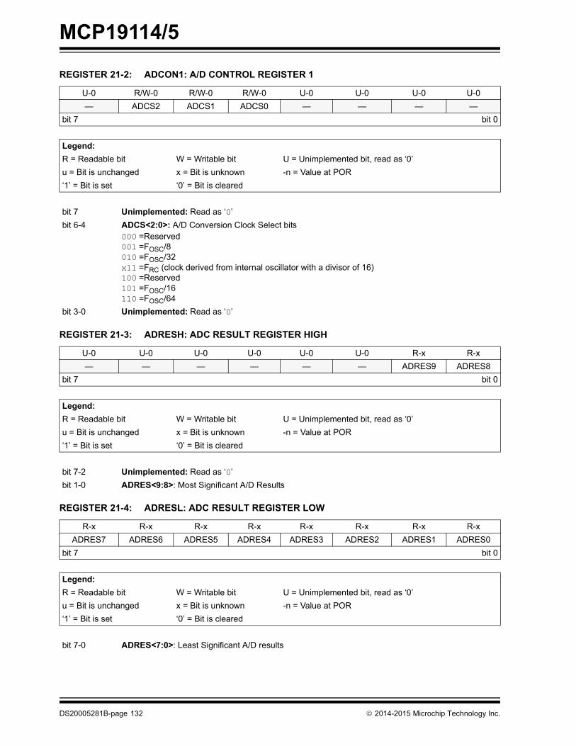
MCP19114/5
REGISTER 21-2: ADCON1: A/D CONTROL REGISTER 1
U-0 R/W-0 R/W-0 R/W-0 U-0 U-0 U-0 U-0— ADCS2 ADCS1 ADCS0 — — — —
bit 7 bit 0
Legend:R = Readable bit W = Writable bit U = Unimplemented bit, read as ‘0’u = Bit is unchanged x = Bit is unknown -n = Value at POR‘1’ = Bit is set ‘0’ = Bit is cleared
bit 7 Unimplemented: Read as ‘0’bit 6-4 ADCS<2:0>: A/D Conversion Clock Select bits
000 =Reserved001 =FOSC/8010 =FOSC/32x11 =FRC (clock derived from internal oscillator with a divisor of 16)100 =Reserved101 =FOSC/16110 =FOSC/64
bit 3-0 Unimplemented: Read as ‘0’
REGISTER 21-3: ADRESH: ADC RESULT REGISTER HIGH
U-0 U-0 U-0 U-0 U-0 U-0 R-x R-x— — — — — — ADRES9 ADRES8
bit 7 bit 0
Legend:R = Readable bit W = Writable bit U = Unimplemented bit, read as ‘0’u = Bit is unchanged x = Bit is unknown -n = Value at POR‘1’ = Bit is set ‘0’ = Bit is cleared
bit 7-2 Unimplemented: Read as ‘0’bit 1-0 ADRES<9:8>: Most Significant A/D Results
REGISTER 21-4: ADRESL: ADC RESULT REGISTER LOW
R-x R-x R-x R-x R-x R-x R-x R-xADRES7 ADRES6 ADRES5 ADRES4 ADRES3 ADRES2 ADRES1 ADRES0
bit 7 bit 0
Legend:R = Readable bit W = Writable bit U = Unimplemented bit, read as ‘0’u = Bit is unchanged x = Bit is unknown -n = Value at POR‘1’ = Bit is set ‘0’ = Bit is cleared
bit 7-0 ADRES<7:0>: Least Significant A/D results
DS20005281B-page 132 2014-2015 Microchip Technology Inc.
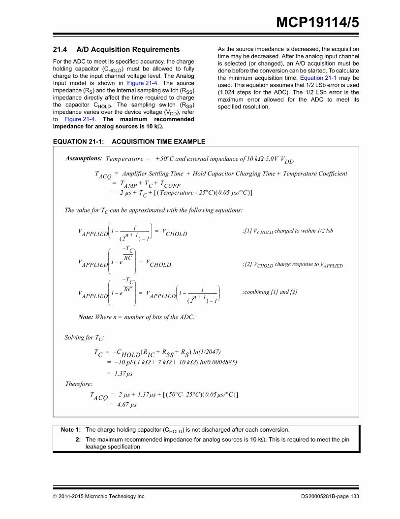
MCP19114/5
21.4 A/D Acquisition RequirementsFor the ADC to meet its specified accuracy, the chargeholding capacitor (CHOLD) must be allowed to fullycharge to the input channel voltage level. The AnalogInput model is shown in Figure 21-4. The sourceimpedance (RS) and the internal sampling switch (RSS)impedance directly affect the time required to chargethe capacitor CHOLD. The sampling switch (RSS)impedance varies over the device voltage (VDD), referto Figure 21-4. The maximum recommendedimpedance for analog sources is 10 k.2014-2015 Microchip Technology Inc.
As the source impedance is decreased, the acquisitiontime may be decreased. After the analog input channelis selected (or changed), an A/D acquisition must bedone before the conversion can be started. To calculatethe minimum acquisition time, Equation 21-1 may beused. This equation assumes that 1/2 LSb error is used(1,024 steps for the ADC). The 1/2 LSb error is themaximum error allowed for the ADC to meet itsspecified resolution.
EQUATION 21-1: ACQUISITION TIME EXAMPLE
Note 1: The charge holding capacitor (CHOLD) is not discharged after each conversion.
2: The maximum recommended impedance for analog sources is 10 k. This is required to meet the pin leakage specification.
TACQ Amplifier Settling Time Hold Capacitor Charging Time Temperature Coefficient+ += TAMP TC TCOFF+ += 2 µs TC Temperature - 25°C 0.05 µs/°C + +=
TC CHOLD RIC RSS RS+ + ln(1/2047)–= 10 pF 1 k 7 k 10 k+ + – ln(0.0004885)=
1.37= µs
VAPPLIED 1 e
TC–
RC----------
–
VAPPLIED 1 1
2n 1+ 1–------------------------------–
=
VAPPLIED 1 1
2n 1+ 1–------------------------------–
VCHOLD=
VAPPLIED 1 e
TC–
RC----------
–
VCHOLD=
;[1] VCHOLD charged to within 1/2 lsb
;[2] VCHOLD charge response to VAPPLIED
;combining [1] and [2]
The value for TC can be approximated with the following equations:
Solving for TC:
Therefore:
Temperature +50°C and external impedance of 10 k 5.0V VDD=Assumptions:
Note: Where n = number of bits of the ADC.
TACQ 2 µs 1.37µs 50°C- 25°C 0.05µs/°C + += 4.67 µs=
DS20005281B-page 133

MCP19114/5
FIGURE 21-4: ANALOG INPUT MODELFIGURE 21-5: ADC TRANSFER FUNCTION
CPINVA
RS
Analog
5 pF
VDD
VT 0.6V
VT 0.6V
RIC 1k SS RSS
CHOLD = 10 pF
VSS/VREF-
6V
Sampling Switch
5V4V3V2V
5 6 7 8 91011
(kW)
VDD
RSS
Note 1: Refer to Section 4.0 “Electrical Characteristics”.
Inputpin
SamplingSwitch
ILEAKAGE(1)
Legend:CHOLD = Sample/Hold Capacitance
CPIN = Input CapacitanceILEAKAGE = Leakage current at the pin due to various junctions
RIC = Interconnect ResistanceRSS = Resistance of Sampling SwitchSS = Sampling SwitchVT = Threshold Voltage
3FFh3FEh
AD
C O
utpu
t Cod
e
3FDh3FCh
03h02h01h00h
Full-Scale
3FBh
0.5 LSB
VREF- Zero-ScaleTransition VREF
+Transition
1.5 LSB
Full-Scale Range
Analog Input Voltage
DS200
05281B-page 134 2014-2015 Microchip Technology Inc.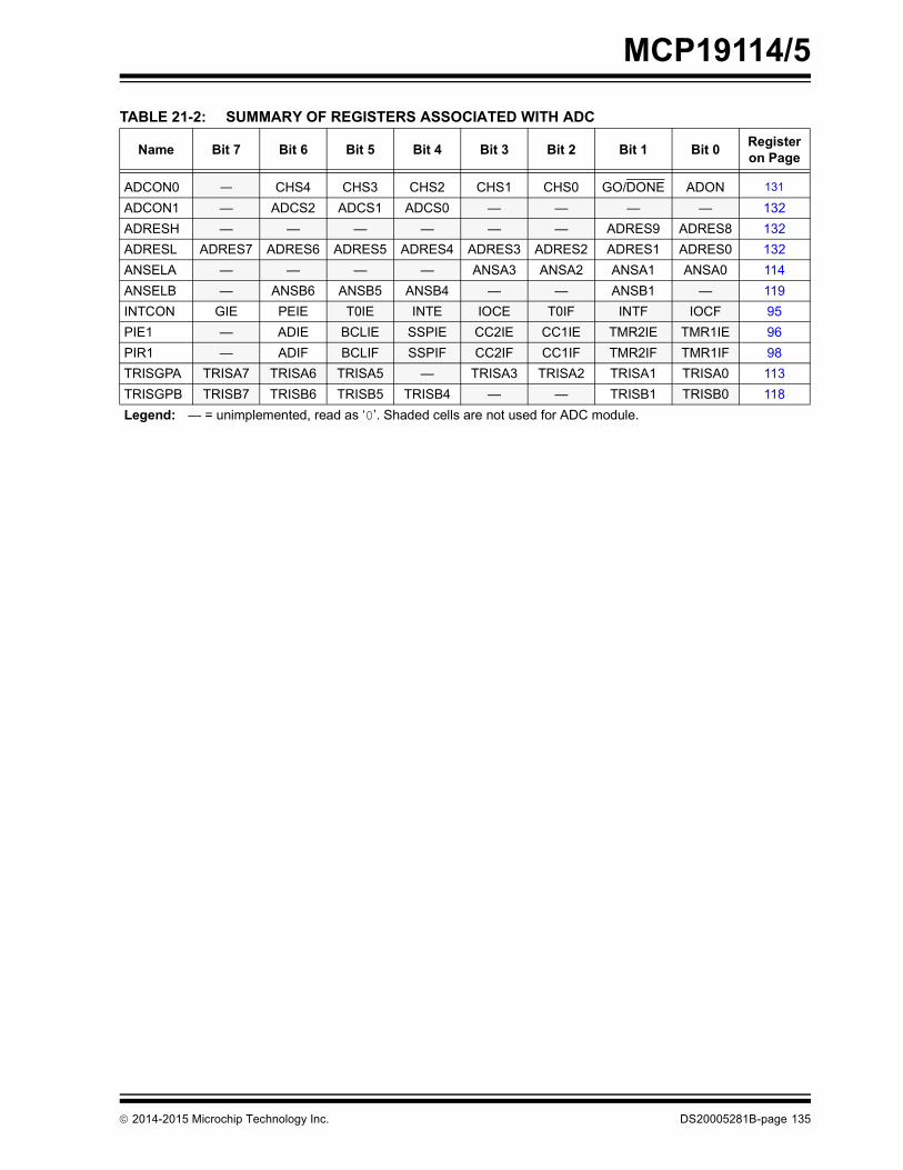
MCP19114/5
TABLE 21-2: SUMMARY OF REGISTERS ASSOCIATED WITH ADC
Name Bit 7 Bit 6 Bit 5 Bit 4 Bit 3 Bit 2 Bit 1 Bit 0 Register on Page
ADCON0 — CHS4 CHS3 CHS2 CHS1 CHS0 GO/DONE ADON 131
ADCON1 — ADCS2 ADCS1 ADCS0 — — — — 132ADRESH — — — — — — ADRES9 ADRES8 132ADRESL ADRES7 ADRES6 ADRES5 ADRES4 ADRES3 ADRES2 ADRES1 ADRES0 132ANSELA — — — — ANSA3 ANSA2 ANSA1 ANSA0 114ANSELB — ANSB6 ANSB5 ANSB4 — — ANSB1 — 119INTCON GIE PEIE T0IE INTE IOCE T0IF INTF IOCF 95PIE1 — ADIE BCLIE SSPIE CC2IE CC1IE TMR2IE TMR1IE 96PIR1 — ADIF BCLIF SSPIF CC2IF CC1IF TMR2IF TMR1IF 98TRISGPA TRISA7 TRISA6 TRISA5 — TRISA3 TRISA2 TRISA1 TRISA0 113TRISGPB TRISB7 TRISB6 TRISB5 TRISB4 — — TRISB1 TRISB0 118Legend: — = unimplemented, read as ‘0’. Shaded cells are not used for ADC module.
2014-2015 Microchip Technology Inc. DS20005281B-page 135

MCP19114/5
NOTES:DS20005281B-page 136
2014-2015 Microchip Technology Inc.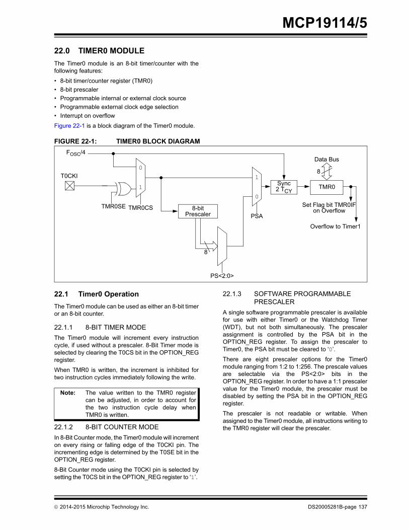
MCP19114/5
22.0 TIMER0 MODULEThe Timer0 module is an 8-bit timer/counter with thefollowing features:
• 8-bit timer/counter register (TMR0)• 8-bit prescaler• Programmable internal or external clock source• Programmable external clock edge selection• Interrupt on overflow
Figure 22-1 is a block diagram of the Timer0 module.
2014-2015 Microchip Technology Inc.
FIGURE 22-1: TIMER0 BLOCK DIAGRAM
T0CKI
TMR0SE
TMR0
PS<2:0>
Data Bus
Set Flag bit TMR0IFon OverflowTMR0CS
0
1
0
18
8
8-bitPrescaler
FOSC/4
PSA
Sync2 TCY
Overflow to Timer1
22.1 Timer0 OperationThe Timer0 module can be used as either an 8-bit timeror an 8-bit counter.
22.1.1 8-BIT TIMER MODEThe Timer0 module will increment every instructioncycle, if used without a prescaler. 8-Bit Timer mode isselected by clearing the T0CS bit in the OPTION_REGregister.
When TMR0 is written, the increment is inhibited fortwo instruction cycles immediately following the write.
22.1.2 8-BIT COUNTER MODEIn 8-Bit Counter mode, the Timer0 module will incrementon every rising or falling edge of the T0CKI pin. Theincrementing edge is determined by the T0SE bit in theOPTION_REG register.
8-Bit Counter mode using the T0CKI pin is selected bysetting the T0CS bit in the OPTION_REG register to ‘1’.
Note: The value written to the TMR0 registercan be adjusted, in order to account forthe two instruction cycle delay whenTMR0 is written.
22.1.3 SOFTWARE PROGRAMMABLE PRESCALER
A single software programmable prescaler is availablefor use with either Timer0 or the Watchdog Timer(WDT), but not both simultaneously. The prescalerassignment is controlled by the PSA bit in theOPTION_REG register. To assign the prescaler toTimer0, the PSA bit must be cleared to ‘0’.
There are eight prescaler options for the Timer0module ranging from 1:2 to 1:256. The prescale valuesare selectable via the PS<2:0> bits in theOPTION_REG register. In order to have a 1:1 prescalervalue for the Timer0 module, the prescaler must bedisabled by setting the PSA bit in the OPTION_REGregister.
The prescaler is not readable or writable. Whenassigned to the Timer0 module, all instructions writing tothe TMR0 register will clear the prescaler.
DS20005281B-page 137
MCP19114/5
22.1.4 SWITCHING PRESCALERBETWEEN TIMER0 AND WDT MODULES
As a result of having the prescaler assigned to eitherTimer0 or the WDT, it is possible to generate anunintended device reset when switching prescalervalues. When changing the prescaler assignment fromTimer0 to the WDT module, the instruction sequenceshown in Example 22-1 must be executed.
EXAMPLE 22-1: CHANGING PRESCALER (TIMER0 WDT)
When changing the prescaler assignment from theWDT to the Timer0 module, the following instructionsequence must be executed (refer to Example 22-2).
EXAMPLE 22-2: CHANGING PRESCALER (WDT TIMER0)
BANKSELTMR0;
CLRWDT ;Clear WDT
CLRFTMR0;Clear TMR0 and
;prescaler
BANKSELOPTION_REG;
BSF OPTION_REG,PSA;Select WDT
CLRWDT ;
;
MOVLWb’11111000’;Mask prescaler
ANDWFOPTION_REG,W;bits
IORLWb’00000101’;Set WDT prescaler
MOVWFOPTION_REG;to 1:32
CLRWDT ;Clear WDT and
;prescaler
BANKSELOPTION_REG;
MOVLWb’11110000’;Mask TMR0 select and
ANDWFOPTION_REG,W;prescaler bits
IORLWb’00000011’;Set prescale to 1:16
MOVWFOPTION_REG;
DS20005281B-page 138
22.1.5 TIMER0 INTERRUPTTimer0 will generate an interrupt when the TMR0register overflows from FFh to 00h. The T0IF interruptflag bit in the INTCON register is set every time theTMR0 register overflows, regardless of whether or notthe Timer0 interrupt is enabled. The T0IF bit can onlybe cleared in software. The Timer0 interrupt enable isthe T0IE bit in the INTCON register.
22.1.6 USING TIMER0 WITH AN EXTERNAL CLOCK
When Timer0 is in Counter mode, the synchronizationof the T0CKI input and the Timer0 register isaccomplished by sampling the prescaler output on theQ2 and Q4 cycles of the internal phase clocks.Therefore, the high and low periods of the externalclock source must meet the timing requirements asshown in Section 4.0 “Electrical Characteristics”.
22.1.7 OPERATION DURING SLEEPTimer0 cannot operate while the processor is in Sleepmode. The contents of the TMR0 register will remainunchanged while the processor is in Sleep mode.
Note: The Timer0 interrupt cannot wake theprocessor from Sleep since the timer isfrozen during Sleep.
TABLE 22-1: SUMMARY OF REGISTERS ASSOCIATED WITH TIMER0
Name Bit 7 Bit 6 Bit 5 Bit 4 Bit 3 Bit 2 Bit 1 Bit 0 Register on Page
INTCON GIE PEIE T0IE INTE IOCIE T0IF INTF IOCIF 95
OPTION_REG RAPU INTEDG T0CS T0SE PSA PS2 PS1 PS0 78TMR0 Timer0 Module Register 137*TRISGPA TRISA7 TRISA6 TRISA5 TRISA4 TRISA3 TRISA2 TRISA1 TRISA0 113Legend: — = Unimplemented locations, read as ‘0’. Shaded cells are not used by the Timer0 module.
* Page provides register information.
2014-2015 Microchip Technology Inc.
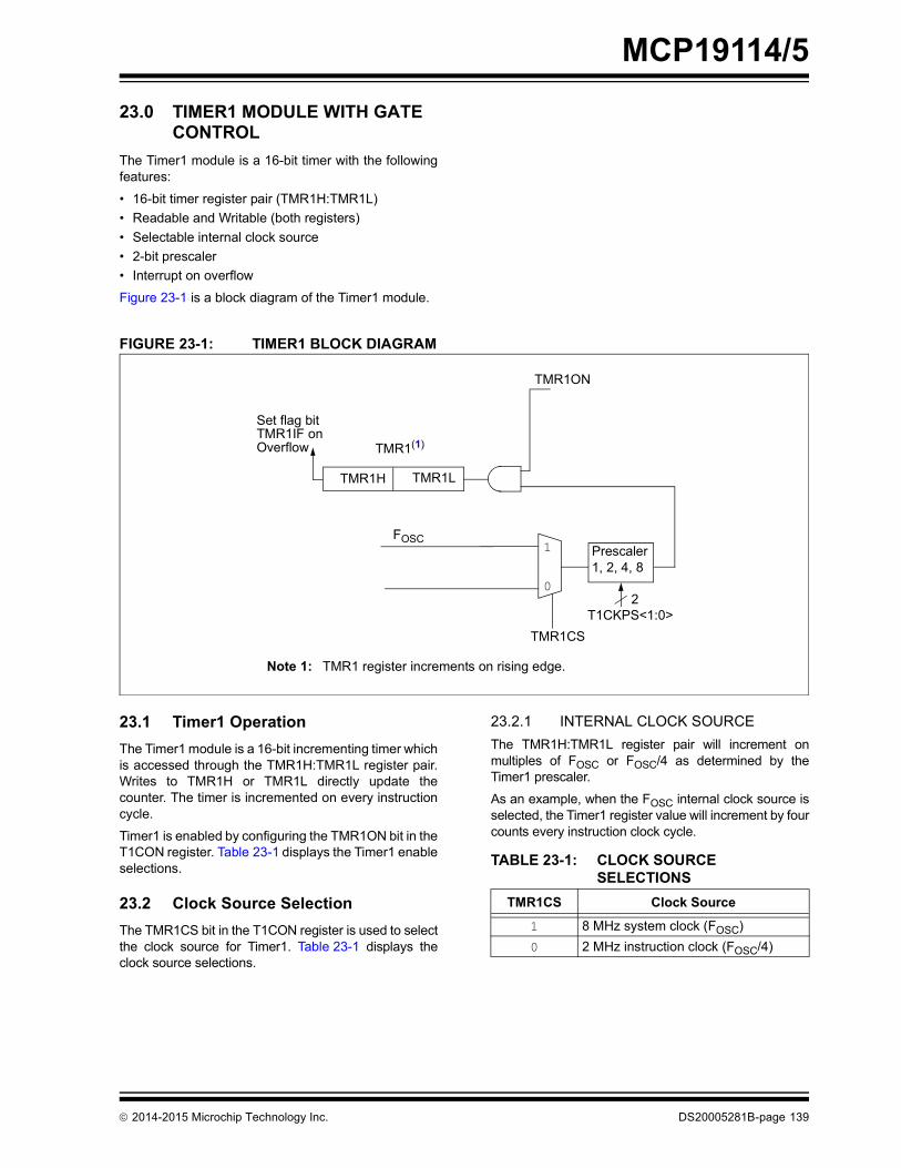
MCP19114/5
23.0 TIMER1 MODULE WITH GATE CONTROL
The Timer1 module is a 16-bit timer with the followingfeatures:
• 16-bit timer register pair (TMR1H:TMR1L)• Readable and Writable (both registers)• Selectable internal clock source• 2-bit prescaler• Interrupt on overflow
Figure 23-1 is a block diagram of the Timer1 module.
2014-2015 Microchip Technology Inc.
FIGURE 23-1: TIMER1 BLOCK DIAGRAM
TMR1H TMR1L
TMR1CST1CKPS<1:0>
1
02
Set flag bitTMR1IF onOverflow
TMR1ON
Note 1: TMR1 register increments on rising edge.
FOSC
TMR1(1)
Prescaler1, 2, 4, 8
23.1 Timer1 OperationThe Timer1 module is a 16-bit incrementing timer whichis accessed through the TMR1H:TMR1L register pair.Writes to TMR1H or TMR1L directly update thecounter. The timer is incremented on every instructioncycle.
Timer1 is enabled by configuring the TMR1ON bit in theT1CON register. Table 23-1 displays the Timer1 enableselections.
23.2 Clock Source SelectionThe TMR1CS bit in the T1CON register is used to selectthe clock source for Timer1. Table 23-1 displays theclock source selections.
23.2.1 INTERNAL CLOCK SOURCEThe TMR1H:TMR1L register pair will increment onmultiples of FOSC or FOSC/4 as determined by theTimer1 prescaler.
As an example, when the FOSC internal clock source isselected, the Timer1 register value will increment by fourcounts every instruction clock cycle.
TABLE 23-1: CLOCK SOURCE SELECTIONS
TMR1CS Clock Source
1 8 MHz system clock (FOSC)0 2 MHz instruction clock (FOSC/4)
DS20005281B-page 139

MCP19114/5
23.3 Timer1 PrescalerTimer1 has four prescaler options, allowing 1, 2, 4 or 8divisions of the clock input. The T1CKPS bits in theT1CON register control the prescale counter. Theprescale counter is not directly readable or writable;however, the prescaler counter is cleared upon a write toTMR1H or TMR1L.23.4 Timer1 InterruptThe Timer1 register pair (TMR1H:TMR1L) incrementsto FFFFh and rolls over to 0000h. When Timer1 rollsover, the Timer1 interrupt flag bit in the PIR1 register isset. To enable the interrupt on rollover, you must setthese bits:
• TMR1ON bit in the T1CON register• TMR1IE bit in the PIE1 register• PEIE bit in the INTCON register• GIE bit in the INTCON register
The interrupt is cleared by clearing the TMR1IF bit inthe Interrupt Service Routine.
Note: The TMR1H:TMR1L register pair and theTMR1IF bit should be cleared beforeenabling interrupts.
DS20005281B-page 140
23.5 Timer1 in SleepUnlike other standard mid-range Timer1 modules, theMCP19114/5 Timer1 module only clocks from an internalsystem clock, and thus cannot run during Sleep mode,nor can it be used to wake the device from this mode.
23.6 Timer1 Control RegisterThe Timer1 Control (T1CON) register, shown inRegister 23-1, is used to control Timer1 and select thevarious features of the Timer1 module.
REGISTER 23-1: T1CON: TIMER1 CONTROL REGISTER
U-0 U-0 R/W-0 R/W-0 U-0 U-0 R/W-0/ R/W-0
— — T1CKPS1 T1CKPS0 — — TMR1CS TMR1ONbit 7 bit 0
Legend:R = Readable bit W = Writable bit U = Unimplemented bit, read as ‘0’u = Bit is unchanged x = Bit is unknown -n = Value at POR‘1’ = Bit is set ‘0’ = Bit is cleared
bit 7-6 Unimplemented: Read as ‘0’bit 5-4 T1CKPS<1:0>: Timer1 Input Clock Prescale Select bits
11 =1:8 Prescale value10 =1:4 Prescale value01 =1:2 Prescale value00 =1:1 Prescale value
bit 3-2 Unimplemented: Read as ‘0’bit 1 TMR1CS: Timer1 Clock Source Control bit
1 = 8 MHz system clock (FOSC)0 = 2 MHz instruction clock (FOSC/4)
bit 0 TMR1ON: Timer1 On bit1 = Enables Timer10 = Stops Timer1, Clears Timer1 gate flip-flop
2014-2015 Microchip Technology Inc.
MCP19114/5
TABLE 23-2: SUMMARY OF REGISTERS ASSOCIATED WITH TIMER1
Name Bit 7 Bit 6 Bit 5 Bit 4 Bit 3 Bit 2 Bit 1 Bit 0 Register on Page
INTCON GIE PEIE T0IE INTE IOCE T0IF INTF IOCF 95PIE1 — ADIE BCLIE SSPIE CC2IE CC1IE TMR2IE TMR1IE 96PIR1 — ADIF BCLIF SSPIF CC2IF CC1IF TMR2IF TMR1IF 98TMR1H Holding Register for the Most Significant Byte of the 16-bit TMR1 Register 139*TMR1L Holding Register for the Least Significant Byte of the 16-bit TMR1 Register 139*T1CON — — T1CKPS1 T1CKPS0 — — TMR1CS TMR1ON 140Legend: — = unimplemented, read as ‘0’. Shaded cells are not used by the Timer1 module.
* Page provides register information.
2014-2015 Microchip Technology Inc. DS20005281B-page 141

MCP19114/5
NOTES:DS20005281B-page 142
2014-2015 Microchip Technology Inc.
MCP19114/5
24.0 TIMER2 MODULEThe Timer2 module is an 8-bit timer with the followingfeatures:
• 8-bit timer register (TMR2)• 8-bit period register (PR2)• Interrupt on TMR2 match with PR2• Software programmable prescaler (1:1, 1:4, 1:16)
Refer to Figure 24-1 for a block diagram of Timer2.
24.1 Timer2 OperationThe clock input to the Timer2 module is the systemclock (FOSC). The clock is fed into the Timer2 prescaler,which has prescale options of 1:1, 1:4 or 1:16. Theoutput of the prescaler is then used to increment theTMR2 register.
The values of TMR2 and PR2 are constantly comparedto determine when they match. TMR2 will incrementfrom 00h until it matches the value in PR2. When amatch occurs, TMR2 is reset to 00h on the nextincrement cycle.
2014-2015 Microchip Technology Inc.
The match output of the Timer2/PR2 comparator isused to set the TMR2IF interrupt flag bit in the PIR1register.
The TMR2 and PR2 registers are both fully readableand writable. On any Reset, the TMR2 register is set to00h and the PR2 register is set to FFh.
Timer2 is turned on by setting the TMR2ON bit in theT2CON register to a ‘1’. Timer2 is turned off by clearingthe TMR2ON bit to a ‘0’.
The Timer2 prescaler is controlled by the T2CKPS bitsin the T2CON register. The prescaler counter arecleared when:
• A write to TMR2 occurs.• A write to T2CON occurs.• Any device reset occurs (Power-On Reset, MCLR
Reset, Watchdog Timer Reset or Brown-Out Reset).
Note: TMR2 is not cleared when T2CON iswritten.
FIGURE 24-1: TIMER2 BLOCK DIAGRAM
Comparator
TMR2 Sets Flag
TMR2
Output
ResetPrescaler
PR2
2
FOSC 1:1, 1:4, 1:8, 1:16
EQ
bit TMR2IF
T2CKPS<1:0>
DS20005281B-page 143
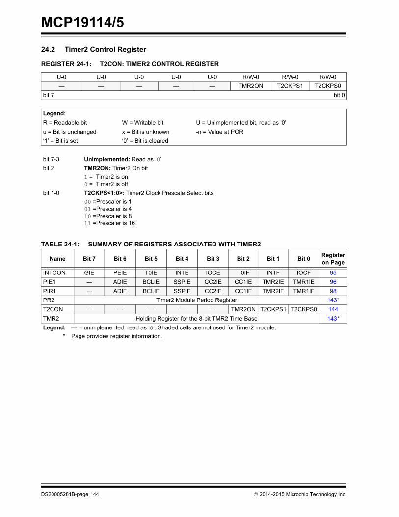
MCP19114/5
24.2 Timer2 Control RegisterREGISTER 24-1: T2CON: TIMER2 CONTROL REGISTER
U-0 U-0 U-0 U-0 U-0 R/W-0 R/W-0 R/W-0— — — — — TMR2ON T2CKPS1 T2CKPS0
bit 7 bit 0
Legend:R = Readable bit W = Writable bit U = Unimplemented bit, read as ‘0’u = Bit is unchanged x = Bit is unknown -n = Value at POR‘1’ = Bit is set ‘0’ = Bit is cleared
bit 7-3 Unimplemented: Read as ‘0’bit 2 TMR2ON: Timer2 On bit
1 = Timer2 is on0 = Timer2 is off
bit 1-0 T2CKPS<1:0>: Timer2 Clock Prescale Select bits00 =Prescaler is 101 =Prescaler is 410 =Prescaler is 811 =Prescaler is 16
TABLE 24-1: SUMMARY OF REGISTERS ASSOCIATED WITH TIMER2
Name Bit 7 Bit 6 Bit 5 Bit 4 Bit 3 Bit 2 Bit 1 Bit 0 Register on Page
INTCON GIE PEIE T0IE INTE IOCE T0IF INTF IOCF 95PIE1 — ADIE BCLIE SSPIE CC2IE CC1IE TMR2IE TMR1IE 96PIR1 — ADIF BCLIF SSPIF CC2IF CC1IF TMR2IF TMR1IF 98PR2 Timer2 Module Period Register 143*T2CON — — — — — TMR2ON T2CKPS1 T2CKPS0 144TMR2 Holding Register for the 8-bit TMR2 Time Base 143*Legend: — = unimplemented, read as ‘0’. Shaded cells are not used for Timer2 module.
* Page provides register information.
DS20005281B-page 144 2014-2015 Microchip Technology Inc.
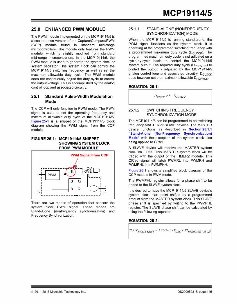
MCP19114/5
25.0 ENHANCED PWM MODULEThe PWM module implemented on the MCP19114/5 isa scaled-down version of the Capture/Compare/PWM(CCP) module found in standard mid-rangemicrocontrollers. The module only features the PWMmodule, which is slightly modified from standardmid-range microcontrollers. In the MCP19114/5, thePWM module is used to generate the system clock orsystem oscillator. This system clock can control theMCP19114/5 switching frequency, as well as set themaximum allowable duty cycle. The PWM moduledoes not continuously adjust the duty cycle to controlthe output voltage. This is accomplished by the analogcontrol loop and associated circuitry.
25.1 Standard Pulse-Width Modulation Mode
The CCP will only function in PWM mode. The PWMsignal is used to set the operating frequency andmaximum allowable duty cycle of the MCP19114/5.Figure 25-1 is a snippet of the MCP19114/5 blockdiagram showing the PWM signal from the CCPmodule.
FIGURE 25-1: MCP19114/5 SNIPPET SHOWING SYSTEM CLOCK FROM PWM MODULE
There are two modes of operation that concern thesystem clock PWM signal. These modes areStand-Alone (nonfrequency synchronization) andFrequency Synchronization.
PWM
S
R
Q
OVOVE
Q
116
PWM Signal From CCP
2014-2015 Microchip Technology Inc.
25.1.1 STAND-ALONE (NONFREQUENCY SYNCHRONIZATION) MODE
When the MCP19114/5 is running stand-alone, thePWM signal functions as the system clock. It isoperating at the programmed switching frequency witha programmed maximum duty cycle (DCLOCK). Theprogrammed maximum duty cycle is not adjusted on acycle-by-cycle basis to control the MCP19114/5system output. The required duty cycle (DPDRVON) tocontrol the output is adjusted by the MCP19114/5analog control loop and associated circuitry. DCLOCKdoes however set the maximum allowable DPDRVON.
EQUATION 25-1:
25.1.2 SWITCHING FREQUENCY SYNCHRONIZATION MODE
The MCP19114/5 can be programmed to be switchingfrequency MASTER or SLAVE devices. The MASTERdevice functions as described in Section 25.1.1“Stand-Alone (NonFrequency Synchronization)Mode” with the exception of the system clock alsobeing applied to GPA1.
A SLAVE device will receive the MASTER systemclock on GPA1. This MASTER system clock will beOR’ed with the output of the TIMER2 module. ThisOR’ed signal will latch PWMRL into PWMRH andPWMPHL into PWMPHH.
Figure 25-1 shows a simplified block diagram of theCCP module in PWM mode.
The PWMPHL register allows for a phase shift to beadded to the SLAVE system clock.
It is desired to have the MCP19114/5 SLAVE device’ssystem clock start point shifted by a programmedamount from the MASTER system clock. This SLAVEphase shift is specified by writing to the PWMPHLregister. The SLAVE phase shift can be calculated byusing the following equation.
EQUATION 25-2:
DBUCK 1 DCLOCK–
SLAVEPHASE SHIFT PWMPHL TOSC T2PRESCALE VALUE =
DS20005281B-page 145
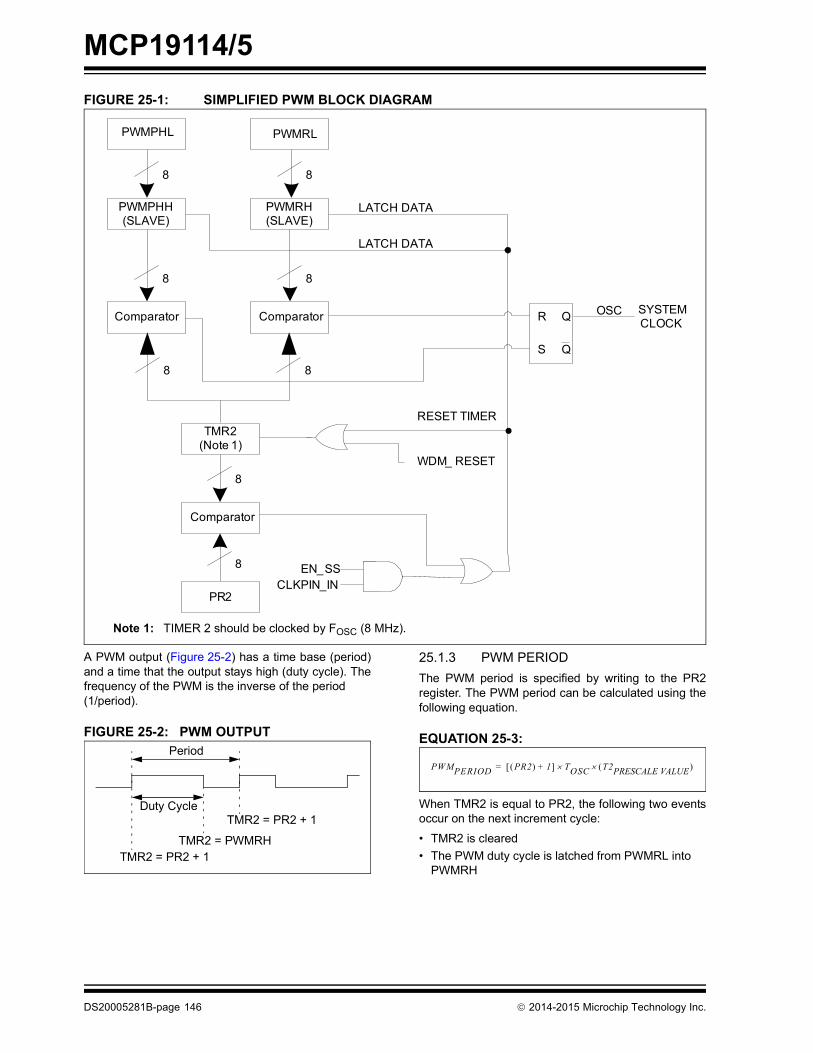
MCP19114/5
FIGURE 25-1: SIMPLIFIED PWM BLOCK DIAGRAMEN_SS
R
S Q
Q OSC SYSTEM CLOCK
LATCH DATA
LATCH DATA
RESET TIMER
8 8
8 8
Comparator Comparator
Comparator
88
8
8
PWMPHL PWMRL
WDM_ RESET
PWMPHH(SLAVE)
PWMRH(SLAVE)
TMR2(Note 1)
PR2CLKPIN_IN
Note 1: TIMER 2 should be clocked by FOSC (8 MHz).
A PWM output (Figure 25-2) has a time base (period)and a time that the output stays high (duty cycle). Thefrequency of the PWM is the inverse of the period(1/period).
FIGURE 25-2: PWM OUTPUTPeriod
Duty Cycle
TMR2 = PR2 + 1TMR2 = PWMRH
TMR2 = PR2 + 1
DS20005281B-page 146
25.1.3 PWM PERIODThe PWM period is specified by writing to the PR2register. The PWM period can be calculated using thefollowing equation.
EQUATION 25-3:
When TMR2 is equal to PR2, the following two eventsoccur on the next increment cycle:
• TMR2 is cleared• The PWM duty cycle is latched from PWMRL into
PWMRH
PWMPERIOD PR2 1+ TOSC T2PRESCALE VALUE =
2014-2015 Microchip Technology Inc.

MCP19114/5
25.1.4 PWM DUTY CYCLE (DCLOCK)The PWM duty cycle (DCLOCK) is specified by writingto the PWMRL register. Up to 8-bit resolution isavailable. The following equation is used to calculatethe PWM duty cycle (DCLOCK).EQUATION 25-4:
PWMDUTY CYCLE PWMRL TOSC T2PRESCALE VALUE =
2014-2015 Microchip Technology Inc.
The PWMRL bits can be written to at any time, but theduty cycle value is not latched into PWMRH until aftera match between PR2 and TMR2 occurs.
25.2 Operation During SleepWhen the device is placed in Sleep, the allocatedtimer will not increment and the state of the module willnot change. If the CLKPIN pin is driving a value, it willcontinue to drive that value. When the device wakesup, it will continue from this state.
TABLE 25-1: SUMMARY OF REGISTERS ASSOCIATED WITH PWM MODULE
Name Bit 7 Bit 6 Bit 5 Bit 4 Bit 3 Bit 2 Bit 1 Bit 0 Register on Page
MODECON MSC1 MSC0 RFB — — — — — 51T2CON — — — — — TMR2ON T2CKPS1 T2CKPS0 144PR2 Timer2 Module Period Register 143PWMRL PWM Register Low Byte 145*PWMPHL Phase Shift Low Byte 145*Legend: — = Unimplemented locations, read as ‘0’. Shaded cells are not used by PWM mode.
* Page provides register information.
DS20005281B-page 147

MCP19114/5
NOTES:DS20005281B-page 148
2014-2015 Microchip Technology Inc.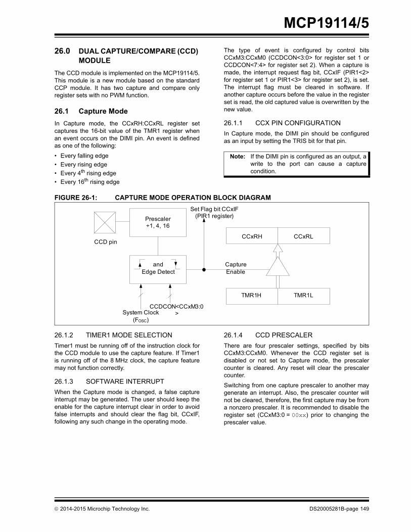
MCP19114/5
26.0 DUAL CAPTURE/COMPARE (CCD) MODULE
The CCD module is implemented on the MCP19114/5.This module is a new module based on the standardCCP module. It has two capture and compare onlyregister sets with no PWM function.
26.1 Capture ModeIn Capture mode, the CCxRH:CCxRL register setcaptures the 16-bit value of the TMR1 register whenan event occurs on the DIMI pin. An event is definedas one of the following:
• Every falling edge• Every rising edge• Every 4th rising edge• Every 16th rising edge
2014-2015 Microchip Technology Inc.
The type of event is configured by control bitsCCxM3:CCxM0 (CCDCON<3:0> for register set 1 orCCDCON<7:4> for register set 2). When a capture ismade, the interrupt request flag bit, CCxIF (PIR1<2>for register set 1 or PIR1<3> for register set 2), is set.The interrupt flag must be cleared in software. Ifanother capture occurs before the value in the registerset is read, the old captured value is overwritten by thenew value.
26.1.1 CCX PIN CONFIGURATIONIn Capture mode, the DIMI pin should be configuredas an input by setting the TRIS bit for that pin.
Note: If the DIMI pin is configured as an output, awrite to the port can cause a capturecondition.
FIGURE 26-1: CAPTURE MODE OPERATION BLOCK DIAGRAM
System Clock (FOSC)
CCDCON<CCxM3:0>
CCxRH CCxRL
TMR1H TMR1L
CaptureEnable
CCD pin
Prescaler÷1, 4, 16
Set Flag bit CCxIF(PIR1 register)
andEdge Detect
26.1.2 TIMER1 MODE SELECTIONTimer1 must be running off of the instruction clock forthe CCD module to use the capture feature. If Timer1is running off of the 8 MHz clock, the capture featuremay not function correctly.
26.1.3 SOFTWARE INTERRUPTWhen the Capture mode is changed, a false captureinterrupt may be generated. The user should keep theenable for the capture interrupt clear in order to avoidfalse interrupts and should clear the flag bit, CCxIF,following any such change in the operating mode.
26.1.4 CCD PRESCALERThere are four prescaler settings, specified by bitsCCxM3:CCxM0. Whenever the CCD register set isdisabled or not set to Capture mode, the prescalercounter is cleared. Any reset will clear the prescalercounter.
Switching from one capture prescaler to another maygenerate an interrupt. Also, the prescaler counter willnot be cleared, therefore, the first capture may be froma nonzero prescaler. It is recommended to disable theregister set (CCxM3:0 = 00xx) prior to changing theprescaler value.
DS20005281B-page 149
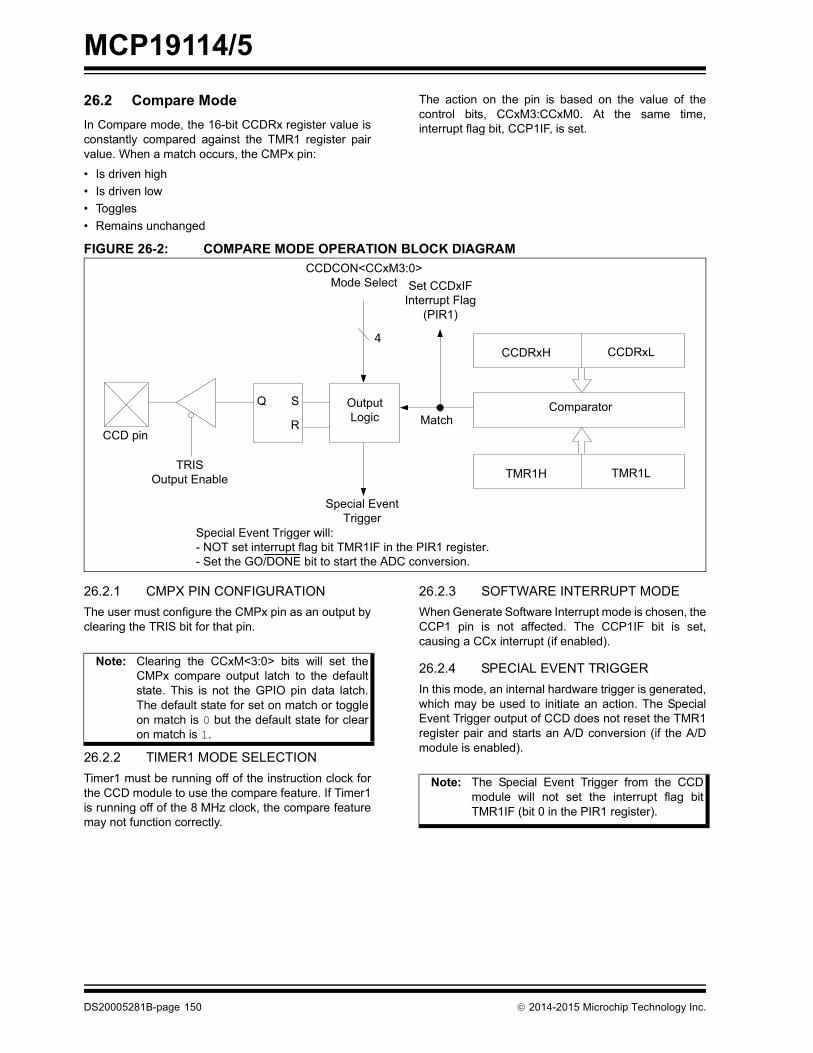
MCP19114/5
26.2 Compare ModeIn Compare mode, the 16-bit CCDRx register value isconstantly compared against the TMR1 register pairvalue. When a match occurs, the CMPx pin:• Is driven high• Is driven low• Toggles• Remains unchanged
DS20005281B-page 150
The action on the pin is based on the value of thecontrol bits, CCxM3:CCxM0. At the same time,interrupt flag bit, CCP1IF, is set.
FIGURE 26-2: COMPARE MODE OPERATION BLOCK DIAGRAM
Special EventTrigger
Match
TRISOutput Enable
CCDCON<CCxM3:0>Mode Select
CCDRxH CCDRxL
CCD pin
Set CCDxIFInterrupt Flag
(PIR1)
Q S
R
OutputLogic
4
TMR1H TMR1L
Comparator
Special Event Trigger will:- NOT set interrupt flag bit TMR1IF in the PIR1 register.- Set the GO/DONE bit to start the ADC conversion.
26.2.1 CMPX PIN CONFIGURATIONThe user must configure the CMPx pin as an output byclearing the TRIS bit for that pin.
26.2.2 TIMER1 MODE SELECTIONTimer1 must be running off of the instruction clock forthe CCD module to use the compare feature. If Timer1is running off of the 8 MHz clock, the compare featuremay not function correctly.
Note: Clearing the CCxM<3:0> bits will set theCMPx compare output latch to the defaultstate. This is not the GPIO pin data latch.The default state for set on match or toggleon match is 0 but the default state for clearon match is 1.
26.2.3 SOFTWARE INTERRUPT MODEWhen Generate Software Interrupt mode is chosen, theCCP1 pin is not affected. The CCP1IF bit is set,causing a CCx interrupt (if enabled).
26.2.4 SPECIAL EVENT TRIGGERIn this mode, an internal hardware trigger is generated,which may be used to initiate an action. The SpecialEvent Trigger output of CCD does not reset the TMR1register pair and starts an A/D conversion (if the A/Dmodule is enabled).
Note: The Special Event Trigger from the CCDmodule will not set the interrupt flag bitTMR1IF (bit 0 in the PIR1 register).
2014-2015 Microchip Technology Inc.
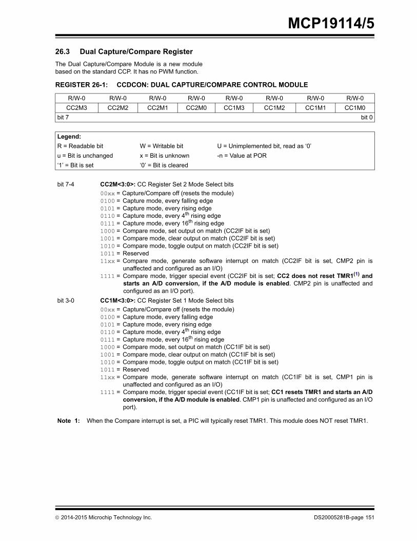
MCP19114/5
26.3 Dual Capture/Compare RegisterThe Dual Capture/Compare Module is a new modulebased on the standard CCP. It has no PWM function.2014-2015 Microchip Technology Inc.
REGISTER 26-1: CCDCON: DUAL CAPTURE/COMPARE CONTROL MODULE
R/W-0 R/W-0 R/W-0 R/W-0 R/W-0 R/W-0 R/W-0 R/W-0CC2M3 CC2M2 CC2M1 CC2M0 CC1M3 CC1M2 CC1M1 CC1M0
bit 7 bit 0
Legend:R = Readable bit W = Writable bit U = Unimplemented bit, read as ‘0’u = Bit is unchanged x = Bit is unknown -n = Value at POR‘1’ = Bit is set ‘0’ = Bit is cleared
bit 7-4 CC2M<3:0>: CC Register Set 2 Mode Select bits00xx = Capture/Compare off (resets the module)0100 = Capture mode, every falling edge0101 = Capture mode, every rising edge0110 = Capture mode, every 4th rising edge0111 = Capture mode, every 16th rising edge1000 = Compare mode, set output on match (CC2IF bit is set)1001 = Compare mode, clear output on match (CC2IF bit is set)1010 = Compare mode, toggle output on match (CC2IF bit is set)1011 = Reserved11xx = Compare mode, generate software interrupt on match (CC2IF bit is set, CMP2 pin is
unaffected and configured as an I/O)1111 = Compare mode, trigger special event (CC2IF bit is set; CC2 does not reset TMR1(1) and
starts an A/D conversion, if the A/D module is enabled. CMP2 pin is unaffected andconfigured as an I/O port).
bit 3-0 CC1M<3:0>: CC Register Set 1 Mode Select bits00xx = Capture/Compare off (resets the module)0100 = Capture mode, every falling edge0101 = Capture mode, every rising edge0110 = Capture mode, every 4th rising edge0111 = Capture mode, every 16th rising edge1000 = Compare mode, set output on match (CC1IF bit is set)1001 = Compare mode, clear output on match (CC1IF bit is set)1010 = Compare mode, toggle output on match (CC1IF bit is set)1011 = Reserved11xx = Compare mode, generate software interrupt on match (CC1IF bit is set, CMP1 pin is
unaffected and configured as an I/O)1111 = Compare mode, trigger special event (CC1IF bit is set; CC1 resets TMR1 and starts an A/D
conversion, if the A/D module is enabled. CMP1 pin is unaffected and configured as an I/Oport).
Note 1: When the Compare interrupt is set, a PIC will typically reset TMR1. This module does NOT reset TMR1.
DS20005281B-page 151

MCP19114/5
NOTES:DS20005281B-page 152
2014-2015 Microchip Technology Inc.
MCP19114/5
27.0 PWM CONTROL LOGICThe PWM Control Logic implements standardcomparator modules to identify events such as inputundervoltage, input overvoltage and desaturationdetection. The control logic takes action in hardware toappropriately enable/disable the output drive(PDRV/SDRV), as well as to set correspondinginterrupt flags to be read by software. This control logicalso defines normal PWM operation. For definition ofindividual bits within the control logic, refer to theSpecial Function Register (SFR) sections.
2014-2015 Microchip Technology Inc.
FIGURE 27-1: PWM CONTROL LOGIC
SDRVEN PDRVEN
OVLOINTP
OVLOINTN OVLOIF
UVLOINTP
UVLOINTN UVLOIF
UVLOEN
OVLOOVLOEN
DELAY
DELAY
SDRV
PDRV
OVINTP
OVINTN OVIF
+-
D
EN
Q OVOUT
OV
Q1
OVEN
PWMSTR_SEN
PWMSTR_PEN
+-
DESATPDESATN
MUX
DEFAULT TODESATP
BG
CDSPOL
CDSINTP
CDSINTNCDSIF
D
EN
Q CDSOUT
Q1
CDSOE
CDSWDEWDM_RESET
S
VSOV_REF
D
EN
Q
D
EN
Q
Q1
UVLOOUT
Q1
OVLOOUT
CDSMUX
UVLO
S
+-
E/AOUTIp
DRUVIF
OTIF
TMPTBY
+-VDRUVLO
+-OT
VDRUVBY
S
R
Q
ONESHOT
SDRV_ON
ONESHOT
200 ns
33 ns
SDRV_ON
PWM
PWM
PWM
DS20005281B-page 153

MCP19114/5
NOTES:DS20005281B-page 154
2014-2015 Microchip Technology Inc.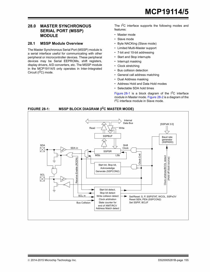
MCP19114/5
28.0 MASTER SYNCHRONOUS SERIAL PORT (MSSP) MODULE
28.1 MSSP Module OverviewThe Master Synchronous Serial Port (MSSP) module isa serial interface useful for communicating with otherperipheral or microcontroller devices. These peripheraldevices may be Serial EEPROMs, shift registers,display drivers, A/D converters, etc. The MSSP modulein the MCP19114/5 only operates in Inter-IntegratedCircuit (I2C) mode.
2014-2015 Microchip Technology Inc.
The I2C interface supports the following modes andfeatures:
• Master mode• Slave mode• Byte NACKing (Slave mode)• Limited Multi-Master support• 7-bit and 10-bit addressing• Start and Stop interrupts• Interrupt masking• Clock stretching• Bus collision detection• General call address matching• Dual Address masking• Address Hold and Data Hold modes• Selectable SDA hold times
Figure 28-1 is a block diagram of the I2C interfacemodule in Master mode. Figure 28-2 is a diagram of theI2C interface module in Slave mode.
FIGURE 28-1: MSSP BLOCK DIAGRAM (I2C MASTER MODE)
Read Write
SSPSR
Start bit, Stop bit,
Start bit detect,
SSPBUF
InternalData Bus
Set/Reset: S, P, SSPSTAT, WCOL, SSPxOV
ShiftClock
MSb LSb
SDA
AcknowledgeGenerate (SSPCON2)
Stop bit detectWrite collision detect
Clock arbitrationState counter forend of XMIT/RCV
SCL
SCL in
Bus Collision
SDA in
Rec
eive
Ena
ble
(RC
EN
)
Clo
ck C
ntl
Clo
ck a
rbitr
ate/
BC
OL
dete
ct(H
old
off c
lock
sou
rce)
[SSPxM 3:0]
Baud rate
Reset SEN, PEN (SSPCON2)
generator(SSPADD)
Address Match detect
Set SSPIF, BCLIF
DS20005281B-page 155

MCP19114/5
FIGURE 28-2: MSSP BLOCK DIAGRAM(I2C SLAVE MODE)
28.2 I2C MODE OVERVIEW
The Inter-Integrated Circuit Bus (I2C) is a multi-masterserial data communication bus. Devices communicatein a master/slave environment, where the masterdevices initiate the communication. A Slave device iscontrolled through addressing.
The I2C bus specifies two signal connections:
• Serial Clock (SCL)• Serial Data (SDA)
Both the SCL and SDA connections are bidirectionalopen-drain lines, each requiring pull-up resistors for thesupply voltage. Pulling the line to ground is considereda logical zero; letting the line float is considered alogical one.
Figure 28-3 shows a typical connection between twodevices configured as master and slave.
The I2C bus can operate with one or more masterdevices and one or more slave devices.
There are four potential modes of operation for a givendevice:
• Master Transmit mode(master is transmitting data to a slave)
• Master Receive mode(master is receiving data from a slave)
• Slave Transmit mode(slave is transmitting data to a master)
• Slave Receive mode(slave is receiving data from a master)
Read Write
SSPSR Reg
Match Detect
SSPADD Reg
Start andStop bit Detect
SSPBUF Reg
InternalData Bus
Addr Match
Set, ResetS, P bits
(SSPSTAT Reg)
SCL
SDA
ShiftClock
MSb LSb
SSPMSK1 Reg
DS20005281B-page 156
To begin communication, a master device starts out inMaster Transmit mode. The master device sends out aStart bit followed by the address byte of the slave itintends to communicate with. This is followed by asingle Read/Write bit, which determines whether themaster intends to transmit to or receive data from theslave device.
If the requested slave exists on the bus, it will respondwith an Acknowledge bit, otherwise known as an ACK.The master then continues in either Transmit mode orReceive mode and the slave continues in thecomplement, either in Receive mode or Transmitmode, respectively.
A Start bit is indicated by a high-to-low transition of theSDA line while the SCL line is held high. Address anddata bytes are sent out Most Significant bit (MSb) first.The Read/Write bit is sent out as a logical one when themaster intends to read data from the slave, and is sentout as a logical zero when it intends to write data to theslave.
FIGURE 28-3: I2C MASTER/SLAVE CONNECTION
The Acknowledge bit (ACK) is an active-low signalwhich holds the SDA line low to indicate to thetransmitter that the slave device has received thetransmitted data and is ready to receive more.
The transition of a data bit is always performed whilethe SCL line is held low. Transitions that occur while theSCL line is held high are used to indicate Start and Stopbits.
If the master intends to write to the slave, it repeatedlysends out a byte of data, with the slave respondingafter each byte with an ACK bit. In this example, themaster device is in Master Transmit mode and theslave is in Slave Receive mode.
If the master intends to read from the slave, itrepeatedly receives a byte of data from the slave andresponds after each byte with an ACK bit. In thisexample, the master device is in Master Receive modeand the slave is Slave Transmit mode.
Master
SCL
SDA
SCL
SDA
SlaveVDD
VDD
2014-2015 Microchip Technology Inc.
MCP19114/5
On the last byte of data communicated, the masterdevice may end the transmission by sending a Stop bit.If the master device is in Receive mode, it sends theStop bit in place of the last ACK bit. A Stop bit isindicated by a low-to-high transition of the SDA linewhile the SCL line is held high.In some cases, the master may want to maintaincontrol of the bus and re-initiate another transmission.If so, the master device may send another Start bit inplace of the Stop bit or last ACK bit when it is in Receivemode.
The I2C bus specifies three message protocols:
• Single message where a master writes data to a slave
• Single message where a master reads data from a slave
• Combined message where a master initiates a minimum of two writes, or two reads, or a combination of writes and reads, to one or more slaves
When one device is transmitting a logical one, or lettingthe line float, and a second device is transmitting alogical zero, or holding the line low, the first device candetect that the line is not a logical one. This detection,when used on the SCL line, is called clock stretching.Clock stretching gives slave devices a mechanism tocontrol the flow of data. When this detection is used onthe SDA line, it is called arbitration. Arbitration ensuresthat there is only one master device communicating atany single time.
28.2.1 CLOCK STRETCHINGWhen a slave device has not completed processingdata, it can delay the transfer of more data through theprocess of Clock Stretching. An addressed slavedevice may hold the SCL clock line low after receivingor sending a bit, indicating that it is not yet ready tocontinue. The master that is communicating with theslave will attempt to raise the SCL line in order totransfer the next bit, but will detect that the clock linehas not yet been released. Because the SCLconnection is open-drain, the slave has the ability tohold that line low until it is ready to continuecommunicating.
Clock stretching allows receivers that cannot keep upwith a transmitter to control the flow of incoming data.
2014-2015 Microchip Technology Inc.
28.2.2 ARBITRATIONEach master device must monitor the bus for Start andStop bits. If the device detects that the bus is busy, itcannot begin a new message until the bus returns to anidle state.
However, two master devices may try to initiate atransmission at or about the same time. When thisoccurs, the process of arbitration begins. Eachtransmitter checks the level of the SDA data line andcompares it to the level that it expects to find. The firsttransmitter to observe that the two levels don't match,loses arbitration and must stop transmitting on the SDAline.
For example, if one transmitter holds the SDA line to alogical one (lets it float) and a second transmitter holdsit to a logical zero (pulls it low), the result is that theSDA line will be low. The first transmitter then observesthat the level of the line is different than expected andconcludes that another transmitter is communicating.
The first transmitter to notice this difference is the onethat loses arbitration and must stop driving the SDAline. If this transmitter is also a master device, it mustalso stop driving the SCL line. It then can monitor thelines for a Stop condition before trying to reissue itstransmission. In the meantime, the other device thathas not noticed any difference between the expectedand actual levels on the SDA line continues with itsoriginal transmission. It can do so without anycomplications, because so far the transmissionappears exactly as expected, with no other transmitterdisturbing the message.
Slave Transmit mode can also be arbitrated, when amaster addresses multiple slaves, but this is lesscommon.
If two master devices are sending a message to twodifferent slave devices at the address stage, the mastersending the lower slave address always winsarbitration. When two master devices send messagesto the same slave address, and addresses cansometimes refer to multiple slaves, the arbitrationprocess must continue into the data stage.
Arbitration usually occurs very rarely, but it is anecessary process for proper multi-master support.
DS20005281B-page 157
MCP19114/5
28.3 I2C MODE OPERATIONAll MSSP I2C communication is byte-oriented andshifted out MSb first. Six SFR registers and twointerrupt flags interface the module with the PICmicrocontroller and with the user’s software. Two pins,SDA and SCL, are exercised by the module tocommunicate with other external I2C devices.
28.3.1 BYTE FORMATAll communication in I2C is done in 9-bit segments. Abyte is sent from a Master to a Slave or vice versa,followed by an Acknowledge bit sent back. After the 8th
falling edge of the SCL line, the device outputting dataon the SDA changes that pin to an input and reads inan acknowledge value on the next clock pulse.
The clock signal, SCL, is provided by the master. Data isvalid to change while the SCL signal is low, and sampledon the rising edge of the clock. Changes on the SDA linewhile the SCL line is high define special conditions onthe bus, explained in the following sections.
DS20005281B-page 158
28.3.2 DEFINITION OF I2C TERMINOLOGYThere is language and terminology in the descriptionof I2C communication that have definitions specific toI2C. Such word usage is defined in Table 28-1 andmay be used in the rest of this document withoutexplanation. The information in this table was adaptedfrom the Philips I2C specification.
28.3.3 SDA AND SCL PINSSelecting any I2C mode with the SSPEN bit set forcesthe SCL and SDA pins to be open-drain. These pinsshould be set by the user to inputs by setting theappropriate TRIS bits.
28.3.4 SDA HOLD TIMEThe hold time of the SDA pin is selected by the SDAHTbit in the SSPCON3 register. Hold time is the time SDAis held valid after the falling edge of SCL. Setting theSDAHT bit selects a longer 300 ns minimum hold timeand may help on buses with large capacitance.
Note: Data is tied to output zero when an I2Cmode is enabled.
TABLE 28-1: I2C BUS TERMSTerm Description
Transmitter The device that shifts data out onto the busReceiver The device that shifts data in from the busMaster The device that initiates a transfer, generates clock signals and terminates a transferSlave The device addressed by the masterMulti-Master A bus with more than one device that can initiate data transfersArbitration Procedure to ensure that only one master at a time controls the bus. Winning arbitration
ensures that the message is not corrupted.Synchronization Procedure to synchronize the clocks of two or more devices on the busIdle No master is controlling the bus and both SDA and SCL lines are highActive Any time one or more master devices are controlling the busAddressed Slave Slave device that has received a matching address and is actively being clocked by a masterMatching Address Address byte that is clocked into a slave that matches the value stored in SSPADDx
Write Request Slave receives a matching address with R/W bit clear and is ready to clock in data
Read Request Master sends an address byte with the R/W bit set, indicating that it wishes to clock data out of the Slave. This data is the next and all following bytes until a Restart or Stop.
Clock Stretching When a device on the bus holds SCL low to stall communicationBus Collision Any time the SDA line is sampled low by the module while it is outputting and expected high
state
2014-2015 Microchip Technology Inc.
MCP19114/5
28.3.5 START CONDITIONThe I2C specification defines a Start condition as atransition of SDA from a high state to a low state, whileSCL line is high. A Start condition is always generatedby the master and signifies the transition of the busfrom an Idle to an Active state. Figure 28-4 shows thewave forms for Start and Stop conditions.A bus collision can occur on a Start condition if themodule samples the SDA line low before asserting itlow. This does not conform to the I2C Specification thatstates no bus collision can occur on a Start.
28.3.6 STOP CONDITIONA Stop condition is a transition of the SDA line fromlow-to-high state while the SCL line is high.
Note: At least one SCL low time must appearbefore a Stop is valid. Therefore, if the SDAline goes low then high again while the SCLline stays high, only the Start condition isdetected.
2014-2015 Microchip Technology Inc.
28.3.7 RESTART CONDITIONA Restart is valid any time that a Stop is valid. A mastercan issue a Restart if it wishes to hold the bus afterterminating the current transfer. A Restart has the sameeffect on the slave that a Start would, resetting all slavelogic and preparing it to clock in an address. The mastermay want to address the same or another slave.
In 10-bit Addressing Slave mode, a Restart is requiredfor the master to clock data out of the addressedslave. Once a slave has been fully addressed,matching both high and low address bytes, the mastercan issue a Restart and the high address byte with theR/W bit set. The slave logic will then hold the clockand prepare to clock out data.
After a full match with R/W clear in 10-bit mode, a priormatch flag is set and maintained. Until a Stopcondition, a high address with R/W clear or a highaddress match fails.
28.3.8 START/STOP CONDITION INTERRUPT MASKING
The SCIE and PCIE bits in the SSPCON3 register canenable the generation of an interrupt in Slave modesthat do not typically support this function. These bitswill have no effect on slave modes where interrupt onStart and Stop detect are already enabled.
FIGURE 28-4: I2C START AND STOP CONDITIONS
FIGURE 28-5: I2C RESTART CONDITION
SDA
SCLP
StopCondition
S
StartCondition
Change ofData Allowed
Change ofData Allowed
RestartCondition
Sr
Change ofData Allowed
Change ofData Allowed
DS20005281B-page 159
MCP19114/5
28.3.9 ACKNOWLEDGE SEQUENCEThe 9th SCL pulse for any transferred byte in I2C isdedicated as an Acknowledge. It allows receivingdevices to respond back to the transmitter by pullingthe SDA line low. The transmitter must release controlof the line during this time to shift in the response. TheAcknowledge (ACK) is an active-low signal, pulling theSDA line low, indicating to the transmitter that thedevice has received the transmitted data and is readyto receive more.The result of an ACK is placed in the ACKSTAT bit inthe SSPCON2 register.
Slave software, when the AHEN and DHEN bits areset, allows the user to set the ACK value sent back tothe transmitter. The ACKDT bit in the SSPCON2register is set/cleared to determine the response.
Slave hardware will generate an ACK response if theAHEN and DHEN bits in the SSPCON3 register areclear.
There are certain conditions where an ACK will not besent by the slave. If the BF bit in the SSPSTAT registeror the SSPOV bit in the SSPCON1 register are setwhen a byte is received, the ACK will not be sent.
When the module is addressed, after the 8th fallingedge of SCL on the bus, the ACKTIM bit in theSSPCON3 register is set. The ACKTIM bit indicatesthe acknowledge time of the active bus. The ACKTIMstatus bit is only active when the AHEN or DHEN bitsare enabled.
28.4 I2C SLAVE MODE OPERATION
The MSSP Slave mode operates in one of the fourmodes selected in the SSPM bits in SSPCON1register. The modes can be divided into 7-bit and10-bit Addressing mode. 10-bit Addressing modeoperates the same as 7-bit, with some additionaloverhead for handling the larger addresses.
Modes with Start and Stop bit interrupts operate thesame as the other modes, with SSPIF additionally gettingset upon detection of a Start, Restart or Stop condition.
28.4.1 SLAVE MODE ADDRESSESThe SSPADD register contains the Slave modeaddress. The first byte received after a Start or Restartcondition is compared against the value stored in thisregister. If the byte matches, the value is loaded intothe SSPBUF register and an interrupt is generated. Ifthe value does not match, the module goes idle and noindication is given to the software that anythinghappened.
The SSPMSK1 register affects the address matchingprocess. Refer to Section 28.4.10 “SSPMSK1Register” for more information.
DS20005281B-page 160
28.4.2 SECOND SLAVE MODE ADDRESSThe SSPADD2 register contains a second 7-bit Slavemode address. The first byte received after a Start orRestart condition is compared against the value storedin this register. If the byte matches, the value is loadedinto the SSPBUF register and an interrupt isgenerated. If the value does not match, the modulegoes idle and no indication is given to the software thatanything happened.
The SSPMSK2 register affects the address matchingprocess. Refer to Section 28.4.10 “SSPMSK1Register” for more information.
28.4.2.1 I2C Slave 7-Bit Addressing ModeIn 7-bit Addressing mode, the LSb of the received databyte is ignored when determining if there is an addressmatch.
28.4.2.2 I2C Slave 10-Bit Addressing ModeIn 10-bit Addressing mode, the first received byte iscompared to the binary value of ‘1 1 1 1 0 A9 A80’. A9 and A8 are the two MSb of the 10-bit addressand are stored in bits 2 and 1 in the SSPADD register.
After the high byte has been acknowledged, the UA bitis set and SCL is held low until the user updatesSSPADD with the low address. The low address byte isclocked in, and all 8 bits are compared to the lowaddress value in SSPADD. Even if there is no addressmatch, SSPIF and UA are set and SCL is held low untilSSPADD is updated to receive a high byte again. WhenSSPADD is updated, the UA bit is cleared. Thisensures the module is ready to receive the highaddress byte on the next communication.
A high and low address match as a write request isrequired at the start of all 10-bit addressingcommunication. A transmission can be initiated byissuing a Restart once the slave is addressed, andclocking in the high address with the R/W bit set. Theslave hardware will then acknowledge the readrequest and prepare to clock out data. This is onlyvalid for a slave after it has received a complete highand low address-byte match.
28.4.3 SLAVE RECEPTIONWhen the R/W bit of a matching received address byteis clear, the R/W bit in the SSPSTAT register is cleared.The received address is loaded into the SSPBUFregister and acknowledged.
When an overflow condition exists for a receivedaddress, then Not Acknowledge is given. An overflowcondition is defined as either bit BF in the SSPSTATregister is set, or bit SSPOV in the SSPCON1 register isset. The BOEN bit in the SSPCON3 register modifies thisoperation. For more information, refer to Register 28-4.
2014-2015 Microchip Technology Inc.
MCP19114/5
An MSSP interrupt is generated for each transferreddata byte. Flag bit SSPIF must be cleared by software.When the SEN bit in the SSPCON2 register is set, SCLwill be held low (clock stretch) following each receivedbyte. The clock must be released by setting the CKPbit in the SSPCON1 register, except sometimes in10-bit mode.
28.4.3.1 7-Bit Addressing ReceptionThis section describes a standard sequence of eventsfor the MSSP module configured as an I2C Slave in7-bit Addressing mode, including all decisions madeby hardware or software and their effect on reception.Figures 28-5 and 28-6 are used as a visual referencefor this description.
This is a step-by-step process of what typically mustbe done to accomplish I2C communication.
1. Start bit detected.2. S bit in the SSPSTAT register is set; SSPIF is set
if interrupt on Start detect is enabled.3. Matching address with R/W bit clear is received.4. The slave pulls SDA low, sending an ACK to the
master, and sets SSPIF bit.5. Software clears the SSPIF bit.6. Software reads received address from SSPBUF
clearing the BF flag.7. If SEN = 1, Slave software sets CKP bit to
release the SCL line.8. The master clocks out a data byte.9. Slave drives SDA low sending an ACK to the
master, and sets SSPIF bit.10. Software clears SSPIF.11. Software reads the received byte from SSPBUF
clearing BF.12. Steps 8–12 are repeated for all received bytes
from the Master.13. Master sends Stop condition, setting P bit in the
SSPSTAT register, and the bus goes idle.
2014-2015 Microchip Technology Inc.
28.4.3.2 7-Bit Reception with AHEN and DHEN
Slave device reception with AHEN and DHEN setoperates the same as without these options with extrainterrupts and clock stretching added after the 8th fallingedge of SCL. These additional interrupts allow the slavesoftware to decide whether it wants the ACK to receiveaddress or data byte, rather than the hardware.
This list describes the steps that need to be taken byslave software to use these options for I2Ccommunication. Figure 28-7 displays a module usingboth address and data holding. Figure 28-8 includesthe operation with the SEN bit in the SSPCON2register set.
1. S bit in the SSPSTAT register is set; SSPIF is setif interrupt on Start detect is enabled.
2. Matching address with R/W bit clear is clockedin. SSPIF is set and CKP cleared after the 8th
falling edge of SCL.3. Slave clears the SSPIF.4. Slave can look at the ACKTIM bit in the
SSPCON3 register to determine if the SSPIFwas after or before the ACK.
5. Slave reads the address value from SSPBUF,clearing the BF flag.
6. Slave sets ACK value clocked out to the masterby setting ACKDT.
7. Slave releases the clock by setting CKP.8. SSPxIF is set after an ACK, not after a NACK.9. If SEN = 1 the slave hardware will stretch the
clock after the ACK.10. Slave clears SSPIF.
11. SSPIF set and CKP cleared after 8th falling edgeof SCL for a received data byte.
12. Slave looks at ACKTIM bit in the SSPCON3register to determine the source of the interrupt.
13. Slave reads the received data from SSPBUFclearing BF.
14. Steps 7-14 are the same for each received databyte.
15. Communication is ended by either the slavesending an ACK = 1 or the master sending aStop condition. If a Stop is sent and Interrupt onStop Detect is disabled, the slave will only knowby polling the P bit in the SSPSTAT register.
Note: SSPIF is still set after the 9th falling edge ofSCL even if there is no clock stretching andBF has been cleared. Only if NACK is sentto Master is SSPIF not set.
DS20005281B-page 161
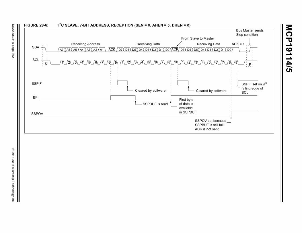
MC
P19114/5
DS
20005281B-page 162
2014-2015 M
icrochip Technology Inc.
ing Data ACK = 1
D3 D2 D1 D0
5 6 7 8
d by software
P
aster
SSPIF set on 9th
falling edge ofSCL
Bus Master sendsStop condition
set becauseF is still full.not sent.
9
FIGURE 28-6: I2C SLAVE, 7-BIT ADDRESS, RECEPTION (SEN = 0, AHEN = 0, DHEN = 0)
Receiving AddressACK
Receiving DataACK
ReceivA7 A6 A5 A4 A3 A2 A1 D7 D6 D5 D4 D3 D2 D1 D0 D7 D6 D5 D4
SDA
SCL
SSPIF
BF
SSPOV
1 2 3 4 5 6 7 8 1 2 3 4 5 6 7 8 1 2 3 4
Cleare
SSPBUF is read
Cleared by software
S
From Slave to M
First byteof data isavailablein SSPBUF
SSPOVSSPBUACK is
9 9

2014-2015 M
icrochip Technology Inc.D
S20005281B
-page 163
MC
P19114/5
FIG
4 D3 D2 D1 D0S
S 5 6 7 8 9 P
S
S
software
ACKeive Data
Bus Master sendsStop condition
SSPIF set on 9th falling edge of SCL
set becauseF is still full.not sent.
n to ‘1’ in software,L
SCL is not heldlow becauseACK = 1
URE 28-7: I2C SLAVE, 7-BIT ADDRESS, RECEPTION (SEN = 1, AHEN = 0, DHEN = 0)
SEN SEN
A7 A6 A5 A4 A3 A2 A1 D7 D6 D5 D4 D3 D2 D1 D0 D7 D6 D5 DDA
CL 1 2 3 4 5 6 7 8 9 1 2 3 4 5 6 7 8 9 1 2 3 4
ACK
CKP
SPOV
BF
SPIF
Cleared by Cleared by software
SSPBUF is read
S
ACKReceive Address Receive Data Rec
R/W=0
Clock is held low until CKP isset to ‘1’
First byteof data isavailablein SSPBUF
SSPOVSSPBUACK is
CKP is written to ‘1’ in software,releasing SCL
CKP is writtereleasing SC

MC
P19114/5
DS
20005281B-page 164
2014-2015 M
icrochip Technology Inc.
d Data
P
D2 D1 D0
6 7 8
BUF
software
9
ACK = 1
No interruptafter not ACKfrom Slave
Slave softwaresets ACKDT tonot ACK
re,
waref SCL
Master sendsStop condition
FIGURE 28-8: I2C SLAVE, 7-BIT ADDRESS, RECEPTION (SEN = 0, AHEN = 1, DHEN = 1)
Receiving Address Receiving Data ReceiveA7 A6 A5 A4 A3 A2 A1 D7 D6 D5 D4 D3
SDA
SCL
BF
CKP
S
P
1 2 3 4 5 6 7 8 9 1 2 3 4 5 6 7 8 9 1 2 3 4 5S
Data is read from SSP
Cleared by
ACK
ACKDT
ACKTIM
SSPIF
ACK
If AHEN = 1,SSPIF is set
SSPIF is set on9th falling edge ofSCL, after ACK
Address is readfrom SSBUF
Slave softwareclears ACKDT toACK the received byte
When AHEN = 1:CKP is cleared by hardwareand SCL is stretched
ACKTIM set by hardwareon 8th falling edge of SCL
When DHEN = 1:CKP is cleared byhardware on 8th fallingedge of SCL
CKP set by softwaSCL is released
ACKTIM cleared byhardware on 9th
rising edge of SCL
ACKTIM set by hardon 8th falling edge o
Master Releases SDAxto slave for ACK sequence
D7 D6 D5 D4 D3 D2 D1 D0
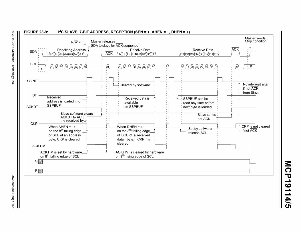
2014-2015 M
icrochip Technology Inc.D
S20005281B
-page 165
MC
P19114/5
FIG
D0
S
A
8 9 P
Master sendsStop condition
ACK
e
No interrupt afterif not ACKfrom Slave
ds
CKP is not clearedif not ACK
URE 28-9: I2C SLAVE, 7-BIT ADDRESS, RECEPTION (SEN = 1, AHEN = 1, DHEN = 1)
Receiving Address Receive Data Receive DataA7 A6 A5 A4 A3 A2 A1 D7 D6 D5 D4 D3 D2 D1 D0 D7 D6 D5 D4 D3 D2 D1
SDA
SCL
SPIF
BF
CKDT
CKP
S
P
S 1 2 3 4 5 6 7 8 9 1 2 3 4 5 6 7 8 9 1 2 3 4 5 6 7
Cleared by software
Slave software clearsACKDT to ACKthe received byte
ACKTIM
R/W = 0
ACK
Master releasesSDA to slave for ACK sequence
Receivedaddress is loaded intoSSPBUF
Received data isavailableon SSPBUF
SSPBUF can beread any time befornext byte is loaded
Slave sennot ACK
When AHEN = 1:on the 8th falling edgeof SCL of an addressbyte, CKP is cleared
When DHEN = 1:on the 8th falling edgeof SCL of a receiveddata byte, CKP iscleared
Set by software,release SCL
ACKTIM is set by hardwareon 8th falling edge of SCL
ACKTIM is cleared by hardwareon 9th rising edge of SCL

MCP19114/5
28.4.4 SLAVE TRANSMISSIONWhen the R/W bit of the incoming address byte is setand an address match occurs, the R/W bit in theSSPSTAT register is set. The received address isloaded into the SSPBUF register and an ACK pulse issent by the slave on the 9th bit.Following the ACK, slave hardware clears the CKP bitand the SCL pin is held low. Refer to Section 28.4.7“Clock Stretching” for more details. By stretching theclock, the master will be unable to assert another clockpulse until the slave is done preparing the transmitdata.
The transmit data must be loaded into the SSPBUFregister, which also loads the SSPSR register. Then theSCL pin should be released by setting the CKP bit inthe SSPCON1 register. The eight data bits are shiftedout on the falling edge of the SCL input. This ensuresthat the SDA signal is valid during the SCL high time.
The ACK pulse from the master-receiver is latched onthe rising edge of the 9th SCL input pulse. This ACKvalue is copied to the ACKSTAT bit in the SSPCON2register. If ACKSTAT is set (not ACK), the data transferis complete. In this case, when the not ACK is latchedby the slave, the slave goes idle and waits for anotheroccurrence of the Start bit. If the SDA line was low(ACK), the next transmit data must be loaded into theSSPBUF register. Again, the SCL pin must be releasedby setting bit CKP.
An MSSP interrupt is generated for each data transferbyte. The SSPIF bit must be cleared by software, andthe SSPSTAT register is used to determine the statusof the byte. The SSPIF bit is set on the falling edge ofthe 9th clock pulse.
28.4.4.1 Slave Mode Bus CollisionA slave receives a Read request and begins shiftingdata out on the SDA line. If a bus collision is detectedand the SBCDE bit in the SSPCON3 register is set, theBCLIF bit in the PIR register is set. Once a bus collisionis detected, the slave goes idle and waits to beaddressed again. The user’s software can use theBCLIF bit to handle a slave bus collision.
DS20005281B-page 166
28.4.4.2 7-Bit TransmissionA master device can transmit a read request to aslave, and then it clocks data out of the slave. The listbelow outlines what software for a slave will need todo to accomplish a standard transmission.Figure 28-10 can be used as a reference to this list.
1. Master sends a Start condition on SDA andSCL.
2. S bit in the SSPSTAT register is set; SSPIF is setif interrupt on Start detect is enabled.
3. Matching address with R/W bit set is received bythe Slave setting SSPIF bit.
4. Slave hardware generates an ACK and setsSSPIF.
5. SSPIF bit is cleared by user.6. Software reads the received address from
SSPBUF, clearing BF.7. R/W is set so CKP was automatically cleared
after the ACK.8. The slave software loads the transmit data into
SSPBUF.9. CKP bit is set releasing SCL, allowing the
master to clock the data out of the slave.10. SSPIF is set after the ACK response from the
master is loaded into the ACKSTAT register.11. SSPIF bit is cleared.12. The slave software checks the ACKSTAT bit to
see if the master wants to clock out more data.
13. Steps 9–13 are repeated for each transmittedbyte.
14. If the master sends a not ACK, the clock is notheld but SSPIF is still set.
15. The master sends a Restart condition or a Stop.16. The slave is no longer addressed.
Note 1: If the master ACKs, the clock will bestretched.
2: ACKSTAT is the only bit updated on therising edge of SCL (9th) rather than on thefalling edge.
2014-2015 Microchip Technology Inc.

2014-2015 M
icrochip Technology Inc.D
S20005281B
-page 167
MC
P19114/5
FIG
smitting Data4 D3 D2 D1 D0
5 6 7 8 9P
ACK
Master sendsStop condition
tically 8th
f SCL
CKP is notheld for notACK
ster’s not ACKopied toKSTAT
URE 28-10: I2C SLAVE, 7-BIT ADDRESS, TRANSMISSION (AHEN = 0)
Receiving Address Automatic Transmitting Data Automatic TranA7 A6 A5 A4 A3 A2 A1 D7 D6 D5 D4 D3 D2 D1 D0 D7 D6 D5 D
1 2 3 4 5 6 7 8 9 1 2 3 4 5 6 7 8 9 1 2 3 4
SDA
SCL
SSPIF
BF
CKP
ACKSTAT
R/W
D/A
S
P
Set by software
Cleared by software
S
R/W = 1
ACK ACK
Received addressis read from SSPBUF
When R/W is set,SCL is alwaysheld low after 9th SCLfalling edge
Data to transmit isloaded into SSPBUF
BF is automacleared afterfalling edge o
Mais cAC
R/W is copied from thematching address byte
Indicates an addresshas been received

MCP19114/5
28.4.4.3 7-Bit Transmission with AddressHold EnabledSetting the AHEN bit in the SSPCON3 registerenables additional clock stretching and interruptgeneration after the 8th falling edge of a receivedmatching address. Once a matching address hasbeen clocked in, CKP is cleared and the SSPIFinterrupt is set.
Figure 28-11 displays a standard waveform of a 7-bitAddress Slave Transmission with AHEN enabled.
1. Bus starts idle.2. Master sends Start condition; the S bit in the
SSPSTAT register is set; SSPIF is set if interrupton Start detect is enabled.
3. Master sends matching address with R/W bitset. After the 8th falling edge of the SCL line, theCKP bit is cleared and SSPIF interrupt isgenerated.
4. Slave software clears SSPIF.5. Slave software reads ACKTIM bit in the
SSPCON3 register and R/W and D/A bits in theSSPSTAT register to determine the source ofthe interrupt.
6. Slave reads the address value from theSSPBUF register, clearing the BF bit.
7. Slave software decides from this information if itwishes to ACK or not ACK, and sets ACKDT bitin the SSPCON2 register accordingly.
8. Slave sets the CKP bit releasing SCL.9. Master clocks in the ACK value from the slave.10. Slave hardware automatically clears the CKP bit
and sets SSPIF after the ACK if the R/W bit isset.
11. Slave software clears SSPIF.12. Slave loads value to transmit to the master into
SSPBUF setting the BF bit.
13. Slave sets CKP bit releasing the clock.14. Master clocks out the data from the slave and
sends an ACK value on the 9th SCL pulse.15. Slave hardware copies the ACK value into the
ACKSTAT bit in the SSPCON2 register.16. Steps 10–15 are repeated for each byte
transmitted to the master from the slave.17. If the master sends a not ACK, the slave
releases the bus, allowing the master to send aStop and end the communication.
Note: SSPBUF cannot be loaded until after theACK.
Note: Master must send a not ACK on the lastbyte to ensure that the slave releases theSCL line to receive a Stop.
DS20005281B-page 168
2014-2015 Microchip Technology Inc.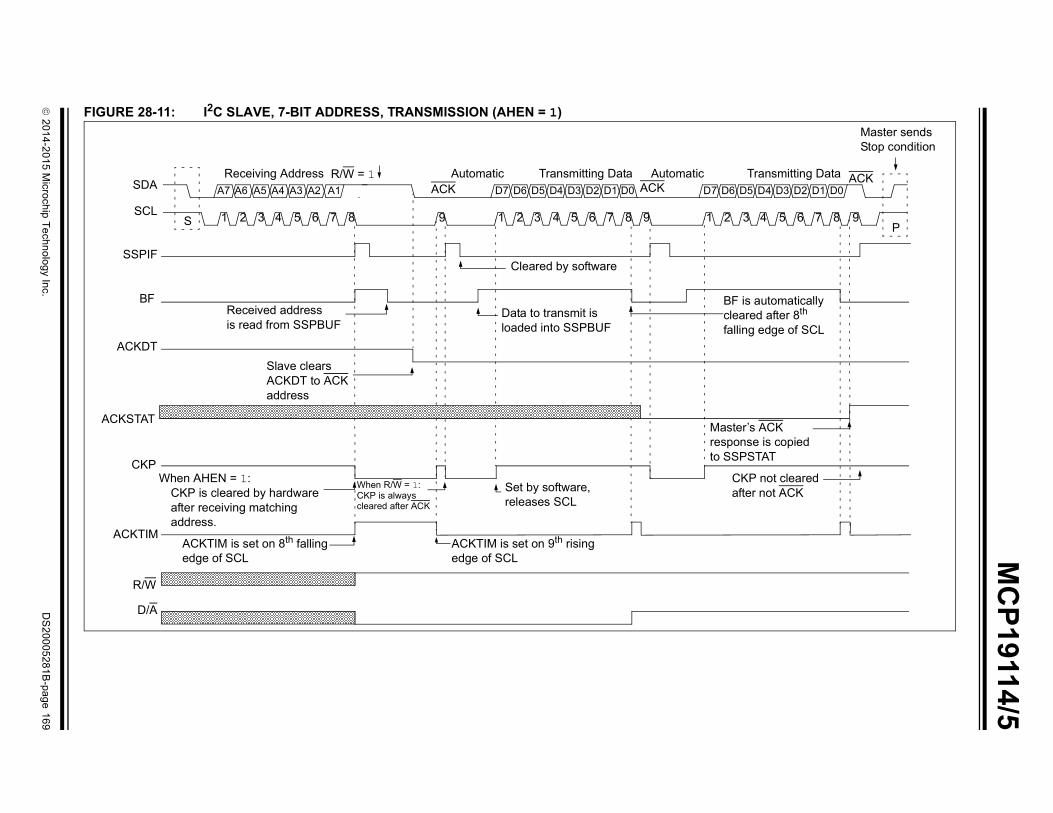
2014-2015 M
icrochip Technology Inc.D
S20005281B
-page 169
MC
P19114/5
FIG
Transmitting Data5 D4 D3 D2 D1 D0
3 4 5 6 7 8 9P
ACK
s automaticallyred after 8th
g edge of SCL
r’s ACKse is copiedSTAT
P not cleareder not ACK
Master sendsStop condition
URE 28-11: I2C SLAVE, 7-BIT ADDRESS, TRANSMISSION (AHEN = 1)
Receiving Address Automatic Transmitting Data AutomaticA7 A6 A5 A4 A3 A2 A1 D7 D6 D5 D4 D3 D2 D1 D0 D7 D6 D
1 2 3 4 5 6 7 8 9 1 2 3 4 5 6 7 8 9 1 2
SDA
SCL
SSPIF
BF
ACKDT
ACKSTAT
CKP
R/W
D/A
Cleared by software
S
ACK ACK
ACKTIM
R/W = 1
Received addressis read from SSPBUF
Slave clearsACKDT to ACKaddress
Data to transmit isloaded into SSPBUF
BF icleafallin
Masteresponto SSP
CKaft
When AHEN = 1:CKP is cleared by hardwareafter receiving matchingaddress.
When R/W = 1:CKP is alwayscleared after ACK
Set by software,releases SCL
ACKTIM is set on 8th fallingedge of SCL
ACKTIM is set on 9th risingedge of SCL

MCP19114/5
28.4.5 SLAVE MODE 10-BIT ADDRESSRECEPTIONThis section describes a standard sequence of eventsfor the MSSP module configured as an I2C Slave in10-bit Addressing mode.
Figure 28-12 is used as a visual reference for thisdescription.
This is a step-by-step process of what must be doneby slave software to accomplish I2C communication:
1. Bus starts idle.2. Master sends Start condition; S bit in the SSP-
STAT register is set; SSPIF is set if interrupt onStart detect is enabled.
3. Master sends matching high address with R/Wbit clear; UA bit in the SSPSTAT register is set.
4. Slave sends ACK and SSPIF is set.5. Software clears the SSPIF bit.6. Software reads received address from SSPBUF,
clearing the BF flag.7. Slave loads low address into SSPADD,
releasing SCL.8. Master sends matching low-address byte to the
Slave; UA bit is set.
9. Slave sends ACK and SSPIF is set.
10. Slave clears SSPIF.11. Slave reads the received matching address
from SSPBUF, clearing BF.12. Slave loads high address into SSPADD.13. Master clocks a data byte to the slave and
clocks out the slave’s ACK on the 9th SCL pulse;SSPIF is set.
14. If SEN bit in the SSPCON2 register is set, CKPis cleared by hardware and the clock isstretched.
15. Slave clears SSPIF.16. Slave reads the received byte from SSPBUF,
clearing BF.17. If SEN is set, the slave sets CKP to release the
SCL.18. Steps 13–17 are repeated for each received
byte.19. Master sends Stop to end the transmission.
Note: Updates to the SSPADD register are notallowed until after the ACK sequence.
Note: If the low address does not match, SSPIFand UA are still set so that the slavesoftware can set SSPADD back to the highaddress. BF is not set because there is nomatch. CKP is unaffected.
DS20005281B-page 170
28.4.6 10-BIT ADDRESSING WITH ADDRESS OR DATA HOLD
Reception using 10-bit addressing with AHEN orDHEN set is the same as with 7-bit modes. The onlydifference is the need to update the SSPADD registerusing the UA bit. All functionality, specifically when theCKP bit is cleared and the SCL line is held low, is thesame. Figure 28-13 can be used as a reference of aslave in 10-bit addressing with AHEN set.
Figure 28-14 shows a standard waveform for a slavetransmitter in 10-bit Addressing mode.
2014-2015 Microchip Technology Inc.

2014-2015 M
icrochip Technology Inc.D
S20005281B
-page 171
MC
P19114/5
FIG
Receive Data
ACKD5 D4 D3 D2 D1 D0
3 4 5 6 7 8 9 P
Master sendsStop condition
is held low CKP = 0
Data is readfrom SSPBUF
et by software,leasing SCL
URE 28-12: I2C SLAVE, 10-BIT ADDRESS, RECEPTION (SEN = 1, AHEN = 0, DHEN = 0)
SSPIF
Receive First Address ByteACK
Receive Second Address Byte
ACK
Receive Data
ACK1 1 1 1 0 A9 A8 A7 A6 A5 A4 A3 A2 A1 A0 D7 D6 D5 D4 D3 D2 D1 D0 D7 D6SDA
SCL
UA
CKP
1 2 3 4 5 6 7 8 9 1 2 3 4 5 6 7 8 9 1 2 3 4 5 6 7 8 9 1 2
Cleared by software
S
BF
Set by hardwareon 9th falling edge
If address matchesSSPADD, it is loaded intoSSPBUF
When UA = 1:SCL is held low
Software updates SSPADDand releases SCL
Receive address isread from SSPBUF
SCLwhile
When SEN = 1:CKP is cleared after9th falling edge of received byte
Sre
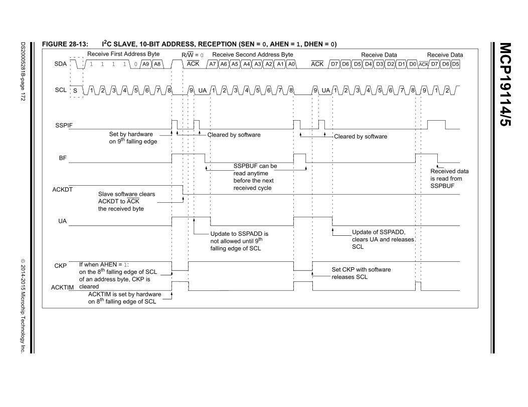
MC
P19114/5
DS
20005281B-page 172
2014-2015 M
icrochip Technology Inc.
Receive DataACK
Receive DataD4 D3 D2 D1 D0 D7 D6 D5
4 5 6 7 8 9 1 2
software
Received datais read fromSSPBUF
ate of SSPADD,rs UA and releases
L
ith softwareL
FIGURE 28-13: I2C SLAVE, 10-BIT ADDRESS, RECEPTION (SEN = 0, AHEN = 1, DHEN = 0) Receive First Address Byte
UA
Receive Second Address Byte
UA
1 1 1 1 0 A9 A8 A7 A6 A5 A4 A3 A2 A1 A0 D7 D6 D5SDA
SCL
SSPIF
BF
ACKDT
UA
CKP
ACKTIM
1 2 3 4 5 6 7 8 9
ACKACK
1 2 3 4 5 6 7 8 9 1 2 3
Cleared by software Cleared by
R/W = 0
S
Set by hardwareon 9th falling edge
Slave software clearsACKDT to ACKthe received byte
SSPBUF can beread anytimebefore the nextreceived cycle
UpdcleaSC
If when AHEN = 1:on the 8th falling edge of SCLof an address byte, CKP iscleared
ACKTIM is set by hardwareon 8th falling edge of SCL
Update to SSPADD isnot allowed until 9th
falling edge of SCL
Set CKP wreleases SC
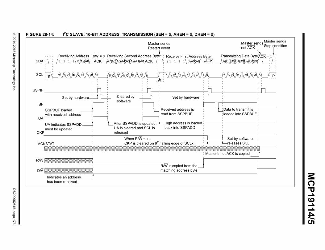
2014-2015 M
icrochip Technology Inc.D
S20005281B
-page 173
MC
P19114/5
FIG
mitting Data ByteD5D4D3D2 D1D0
3 4 5 6 7 8 9
ACK = 1
P
Master sendsnot ACK
Master sendsStop condition
a to transmit ised into SSPBUF
et by softwareleases SCL
K is copied
URE 28-14: I2C SLAVE, 10-BIT ADDRESS, TRANSMISSION (SEN = 0, AHEN = 0, DHEN = 0)
Receiving AddressACK
Receiving Second Address Byte
Sr
Receive First Address ByteACK
Trans1 1 1 1 0 A9 A8 A7 A6 A5 A4 A3 A2 A1 A0 1 1 1 1 0 A9 A8 D7 D6SDA
SCL
SSPIF
BF
UA
CKP
R/W
D/A
1 2 3 4 5 6 7 8 9 1 2 3 4 5 6 7 8 9 1 2 3 4 5 6 7 8 9 1 2
ACKR/W = 0
S
Set by hardware
ACKSTAT
Set by hardware
Master sendsRestart event
Cleared bysoftware
SSPBUF loadedwith received address
UA indicates SSPADDmust be updated
After SSPADD is updated.UA is cleared and SCL isreleased
Received address isread from SSPBUF
High address is loadedback into SSPADD
R/W is copied from thematching address byte
Datload
Sre
Master’s not AC
Indicates an addresshas been received
When R/W = 1:CKP is cleared on 9th falling edge of SCLx
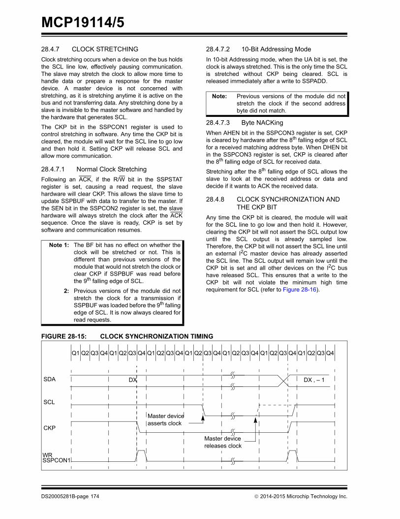
MCP19114/5
28.4.7 CLOCK STRETCHINGClock stretching occurs when a device on the bus holdsthe SCL line low, effectively pausing communication.The slave may stretch the clock to allow more time tohandle data or prepare a response for the masterdevice. A master device is not concerned withstretching, as it is stretching anytime it is active on thebus and not transferring data. Any stretching done by aslave is invisible to the master software and handled bythe hardware that generates SCL.The CKP bit in the SSPCON1 register is used tocontrol stretching in software. Any time the CKP bit iscleared, the module will wait for the SCL line to go lowand then hold it. Setting CKP will release SCL andallow more communication.
28.4.7.1 Normal Clock StretchingFollowing an ACK, if the R/W bit in the SSPSTATregister is set, causing a read request, the slavehardware will clear CKP. This allows the slave time toupdate SSPBUF with data to transfer to the master. Ifthe SEN bit in the SSPCON2 register is set, the slavehardware will always stretch the clock after the ACKsequence. Once the slave is ready, CKP is set bysoftware and communication resumes.
Note 1: The BF bit has no effect on whether theclock will be stretched or not. This isdifferent than previous versions of themodule that would not stretch the clock orclear CKP if SSPBUF was read beforethe 9th falling edge of SCL.
2: Previous versions of the module did notstretch the clock for a transmission ifSSPBUF was loaded before the 9th fallingedge of SCL. It is now always cleared forread requests.
DS20005281B-page 174
28.4.7.2 10-Bit Addressing ModeIn 10-bit Addressing mode, when the UA bit is set, theclock is always stretched. This is the only time the SCLis stretched without CKP being cleared. SCL isreleased immediately after a write to SSPADD.
28.4.7.3 Byte NACKingWhen AHEN bit in the SSPCON3 register is set, CKPis cleared by hardware after the 8th falling edge of SCLfor a received matching address byte. When DHEN bitin the SSPCON3 register is set, CKP is cleared afterthe 8th falling edge of SCL for received data.
Stretching after the 8th falling edge of SCL allows theslave to look at the received address or data anddecide if it wants to ACK the received data.
28.4.8 CLOCK SYNCHRONIZATION AND THE CKP BIT
Any time the CKP bit is cleared, the module will waitfor the SCL line to go low and then hold it. However,clearing the CKP bit will not assert the SCL output lowuntil the SCL output is already sampled low.Therefore, the CKP bit will not assert the SCL line untilan external I2C master device has already assertedthe SCL line. The SCL output will remain low until theCKP bit is set and all other devices on the I2C bushave released SCL. This ensures that a write to theCKP bit will not violate the minimum high timerequirement for SCL (refer to Figure 28-16).
Note: Previous versions of the module did notstretch the clock if the second addressbyte did not match.
FIGURE 28-15: CLOCK SYNCHRONIZATION TIMING
SDA
SCL
DX ‚ – 1DX
WR
Q1 Q2 Q3 Q4 Q1 Q2 Q3 Q4 Q1 Q2 Q3 Q4 Q1 Q2 Q3 Q4 Q1 Q2 Q3 Q4 Q1 Q2 Q3 Q4 Q1 Q2 Q3 Q4
SSPCON1
CKP
Master deviceasserts clock
Master devicereleases clock
2014-2015 Microchip Technology Inc.
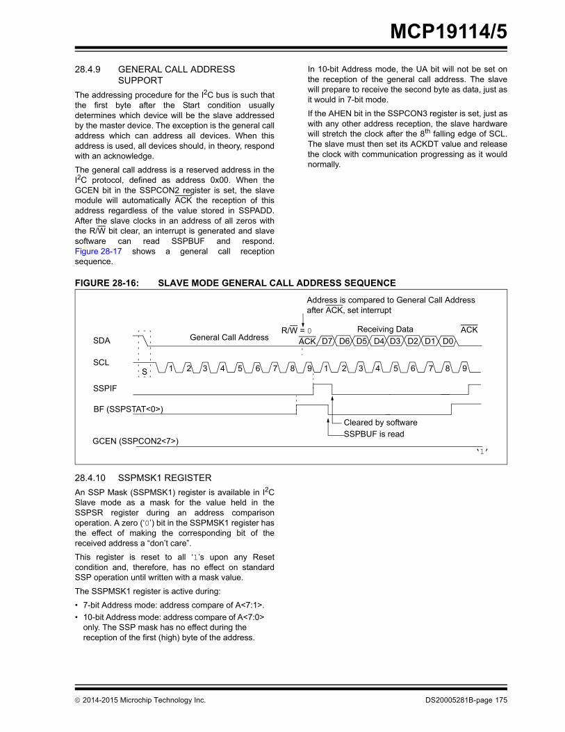
MCP19114/5
28.4.9 GENERAL CALL ADDRESSSUPPORTThe addressing procedure for the I2C bus is such thatthe first byte after the Start condition usuallydetermines which device will be the slave addressedby the master device. The exception is the general calladdress which can address all devices. When thisaddress is used, all devices should, in theory, respondwith an acknowledge.
The general call address is a reserved address in theI2C protocol, defined as address 0x00. When theGCEN bit in the SSPCON2 register is set, the slavemodule will automatically ACK the reception of thisaddress regardless of the value stored in SSPADD.After the slave clocks in an address of all zeros withthe R/W bit clear, an interrupt is generated and slavesoftware can read SSPBUF and respond.Figure 28-17 shows a general call receptionsequence.
2014-2015 Microchip Technology Inc.
In 10-bit Address mode, the UA bit will not be set onthe reception of the general call address. The slavewill prepare to receive the second byte as data, just asit would in 7-bit mode.
If the AHEN bit in the SSPCON3 register is set, just aswith any other address reception, the slave hardwarewill stretch the clock after the 8th falling edge of SCL.The slave must then set its ACKDT value and releasethe clock with communication progressing as it wouldnormally.
FIGURE 28-16: SLAVE MODE GENERAL CALL ADDRESS SEQUENCE
SDA
SCLS
SSPIF
BF (SSPSTAT<0>)Cleared by softwareSSPBUF is read
R/W = 0
ACKGeneral Call AddressReceiving Data ACK
1 2 3 4 5 6 7 8 9 1 2 3 4 5 6 7 8 9
D7 D6 D5 D4 D3 D2 D1 D0
GCEN (SSPCON2<7>)‘1’
Address is compared to General Call Addressafter ACK, set interrupt
28.4.10 SSPMSK1 REGISTERAn SSP Mask (SSPMSK1) register is available in I2CSlave mode as a mask for the value held in theSSPSR register during an address comparisonoperation. A zero (‘0’) bit in the SSPMSK1 register hasthe effect of making the corresponding bit of thereceived address a “don’t care”.
This register is reset to all ‘1’s upon any Resetcondition and, therefore, has no effect on standardSSP operation until written with a mask value.
The SSPMSK1 register is active during:
• 7-bit Address mode: address compare of A<7:1>.• 10-bit Address mode: address compare of A<7:0>
only. The SSP mask has no effect during the reception of the first (high) byte of the address.
DS20005281B-page 175
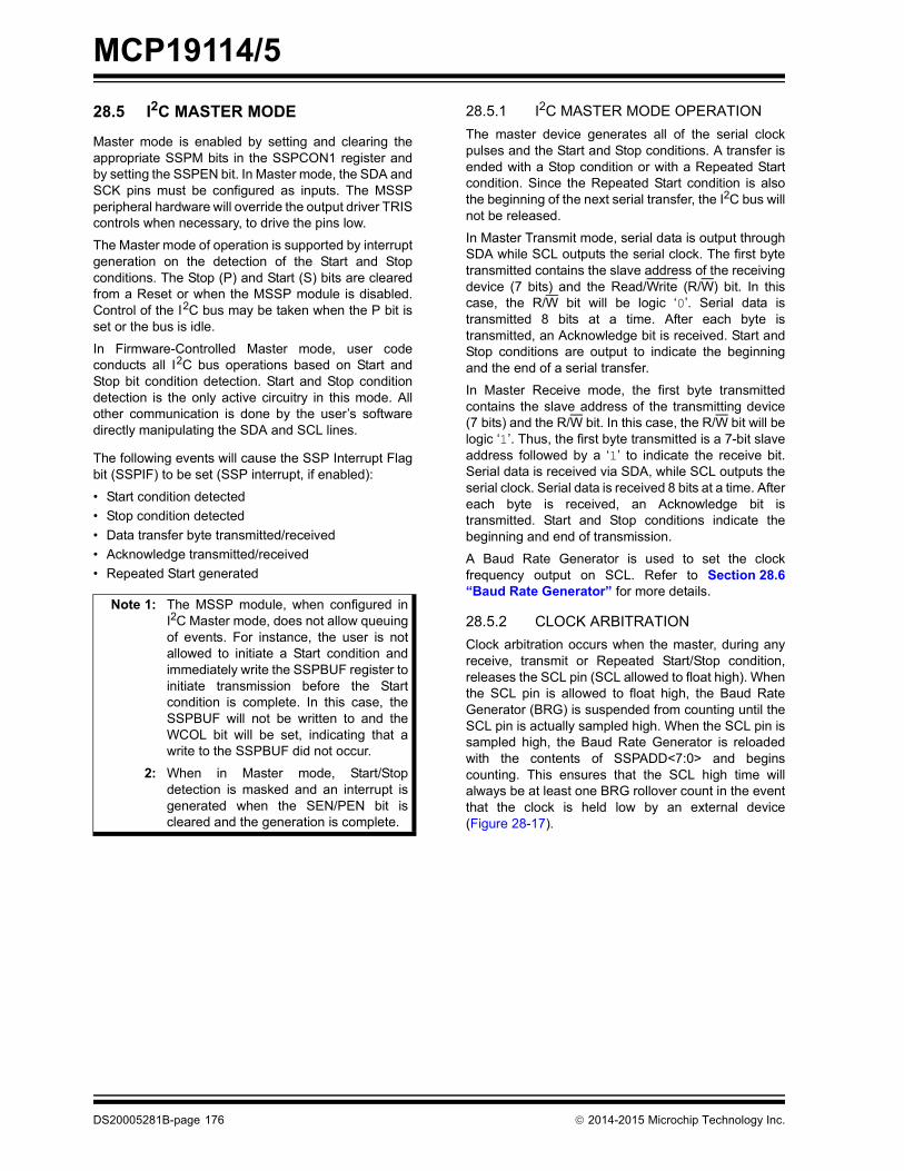
MCP19114/5
28.5 I2C MASTER MODEMaster mode is enabled by setting and clearing theappropriate SSPM bits in the SSPCON1 register andby setting the SSPEN bit. In Master mode, the SDA andSCK pins must be configured as inputs. The MSSPperipheral hardware will override the output driver TRIScontrols when necessary, to drive the pins low.
The Master mode of operation is supported by interruptgeneration on the detection of the Start and Stopconditions. The Stop (P) and Start (S) bits are clearedfrom a Reset or when the MSSP module is disabled.Control of the I2C bus may be taken when the P bit isset or the bus is idle.
In Firmware-Controlled Master mode, user codeconducts all I2C bus operations based on Start andStop bit condition detection. Start and Stop conditiondetection is the only active circuitry in this mode. Allother communication is done by the user’s softwaredirectly manipulating the SDA and SCL lines.
The following events will cause the SSP Interrupt Flagbit (SSPIF) to be set (SSP interrupt, if enabled):
• Start condition detected• Stop condition detected• Data transfer byte transmitted/received• Acknowledge transmitted/received• Repeated Start generated
Note 1: The MSSP module, when configured inI2C Master mode, does not allow queuingof events. For instance, the user is notallowed to initiate a Start condition andimmediately write the SSPBUF register toinitiate transmission before the Startcondition is complete. In this case, theSSPBUF will not be written to and theWCOL bit will be set, indicating that awrite to the SSPBUF did not occur.
2: When in Master mode, Start/Stopdetection is masked and an interrupt isgenerated when the SEN/PEN bit iscleared and the generation is complete.
DS20005281B-page 176
28.5.1 I2C MASTER MODE OPERATIONThe master device generates all of the serial clockpulses and the Start and Stop conditions. A transfer isended with a Stop condition or with a Repeated Startcondition. Since the Repeated Start condition is alsothe beginning of the next serial transfer, the I2C bus willnot be released.
In Master Transmit mode, serial data is output throughSDA while SCL outputs the serial clock. The first bytetransmitted contains the slave address of the receivingdevice (7 bits) and the Read/Write (R/W) bit. In thiscase, the R/W bit will be logic ‘0’. Serial data istransmitted 8 bits at a time. After each byte istransmitted, an Acknowledge bit is received. Start andStop conditions are output to indicate the beginningand the end of a serial transfer.
In Master Receive mode, the first byte transmittedcontains the slave address of the transmitting device(7 bits) and the R/W bit. In this case, the R/W bit will belogic ‘1’. Thus, the first byte transmitted is a 7-bit slaveaddress followed by a ‘1’ to indicate the receive bit.Serial data is received via SDA, while SCL outputs theserial clock. Serial data is received 8 bits at a time. Aftereach byte is received, an Acknowledge bit istransmitted. Start and Stop conditions indicate thebeginning and end of transmission.
A Baud Rate Generator is used to set the clockfrequency output on SCL. Refer to Section 28.6“Baud Rate Generator” for more details.
28.5.2 CLOCK ARBITRATIONClock arbitration occurs when the master, during anyreceive, transmit or Repeated Start/Stop condition,releases the SCL pin (SCL allowed to float high). Whenthe SCL pin is allowed to float high, the Baud RateGenerator (BRG) is suspended from counting until theSCL pin is actually sampled high. When the SCL pin issampled high, the Baud Rate Generator is reloadedwith the contents of SSPADD<7:0> and beginscounting. This ensures that the SCL high time willalways be at least one BRG rollover count in the eventthat the clock is held low by an external device(Figure 28-17).
2014-2015 Microchip Technology Inc.

MCP19114/5
FIGURE 28-17: BAUD RATE GENERATOR TIMING WITH CLOCK ARBITRATIONSDA
SCL
DX ‚ – 1DX
03h 02h 01h 00h (hold off) 03h 02h
SCL allowed to transition highSCL deasserted but slave holdsSCL low (clock arbitration)
BGR decrements onQ2 and Q4 cycles
BRGValue
BRGReload
SCL is sampled high, reload takesplace and BRG starts its count
28.5.3 WCOL STATUS FLAGIf the user writes the SSPBUF when a Start, Restart,Stop, Receive or Transmit sequence is in progress, theWCOL is set and the contents of the buffer areunchanged (the write does not occur). Any time theWCOL bit is set, it indicates that an action on SSPBUFwas attempted while the module was not idle.
28.5.4 I2C MASTER MODE START CONDITION TIMING
To initiate a Start condition, the user sets the StartEnable bit, SEN, in the SSPCON2 register. If the SDAand SCL pins are sampled high, the Baud RateGenerator is reloaded with the contents ofSSPADD<7:0> and starts its count. If SCL and SDAare both sampled high when the Baud Rate Generatortimes out (TBRG), the SDA pin is driven low. The action
Note: Because queuing of events is not allowed,writing to the lower 5 bits in the SSPCON2register is disabled until the Start conditionis complete.
2014-2015 Microchip Technology Inc.
of the SDA being driven low while SCL is high is theStart condition and causes the S bit in the SSPSTAT1register to be set. Following this, the Baud RateGenerator is reloaded with the contents ofSSPADD<7:0> and resumes its count. When the BaudRate Generator times out (TBRG), the SEN bit in theSSPCON2 register will be automatically cleared byhardware; the Baud Rate Generator is suspended,leaving the SDA line held low and the Start condition iscomplete.
Note 1: If, at the beginning of the Start condition,the SDA and SCL pins are alreadysampled low, or if, during the Startcondition, the SCL line is sampled lowbefore the SDA line is driven low, a buscollision occurs, the Bus CollisionInterrupt Flag, BCLIF, is set, the Startcondition is aborted and the I2C module isreset into its idle state.
2: The Philips I2C Specification states that abus collision cannot occur on a Start.
FIGURE 28-18: FIRST START BIT TIMING
SDA
SCLS
TBRG
1st bit 2nd bit
TBRG
SDA = 1, SCL = 1
Write to SSPBUF occurs hereTBRG
TBRG
Write to SEN bit occurs here Set S bit (SSPSTAT<3>)At completion of Start bit,hardware clears SEN bitand sets SSPIF bit
DS20005281B-page 177
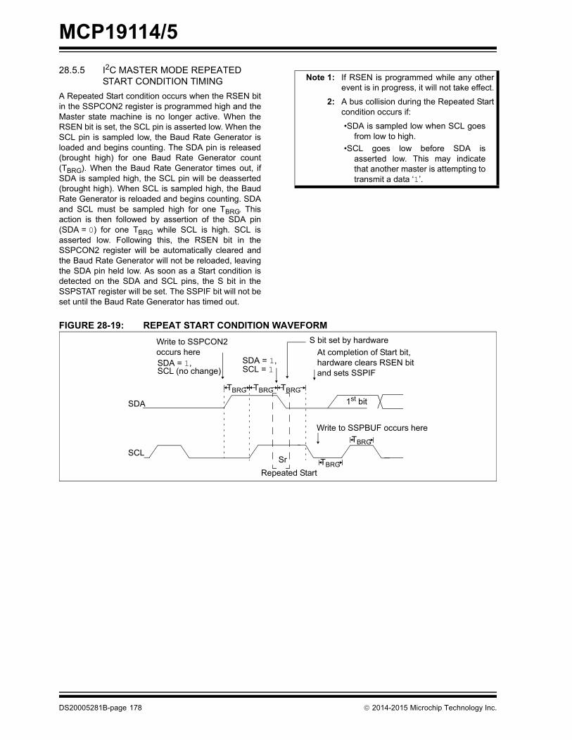
MCP19114/5
28.5.5 I2C MASTER MODE REPEATEDSTART CONDITION TIMINGA Repeated Start condition occurs when the RSEN bitin the SSPCON2 register is programmed high and theMaster state machine is no longer active. When theRSEN bit is set, the SCL pin is asserted low. When theSCL pin is sampled low, the Baud Rate Generator isloaded and begins counting. The SDA pin is released(brought high) for one Baud Rate Generator count(TBRG). When the Baud Rate Generator times out, ifSDA is sampled high, the SCL pin will be deasserted(brought high). When SCL is sampled high, the BaudRate Generator is reloaded and begins counting. SDAand SCL must be sampled high for one TBRG. Thisaction is then followed by assertion of the SDA pin(SDA = 0) for one TBRG while SCL is high. SCL isasserted low. Following this, the RSEN bit in theSSPCON2 register will be automatically cleared andthe Baud Rate Generator will not be reloaded, leavingthe SDA pin held low. As soon as a Start condition isdetected on the SDA and SCL pins, the S bit in theSSPSTAT register will be set. The SSPIF bit will not beset until the Baud Rate Generator has timed out.
DS20005281B-page 178
Note 1: If RSEN is programmed while any otherevent is in progress, it will not take effect.
2: A bus collision during the Repeated Startcondition occurs if:
•SDA is sampled low when SCL goesfrom low to high.
•SCL goes low before SDA isasserted low. This may indicatethat another master is attempting totransmit a data ‘1’.
FIGURE 28-19: REPEAT START CONDITION WAVEFORM
SDA
SCL
Repeated Start
Write to SSPBUF occurs here
1st bit
S bit set by hardware
TBRG
TBRG
SDA = 1, SDA = 1, SCL (no change) SCL = 1
TBRG TBRG TBRG
Sr
Write to SSPCON2occurs here At completion of Start bit,
hardware clears RSEN bitand sets SSPIF
2014-2015 Microchip Technology Inc.
MCP19114/5
28.5.6 I2C MASTER MODETRANSMISSIONTransmission of a data byte, a 7-bit address or theother half of a 10-bit address is accomplished by simplywriting a value to the SSPBUF register. This action willset the Buffer Full (BF) flag bit and allow the Baud RateGenerator to begin counting and start the nexttransmission. Each bit of address/data will be shiftedout onto the SDA pin after the falling edge of SCL isasserted. SCL is held low for one Baud Rate Generatorrollover count (TBRG). Data should be valid before SCLis released high. When the SCL pin is released high, itis held that way for TBRG. The data on the SDA pin mustremain stable for that duration and some hold time afterthe next falling edge of SCL. After the 8th bit is shiftedout (the falling edge of the 8th clock), the BF flag iscleared and the master releases the SDA. This allowsthe slave device being addressed to respond with anACK bit during the 9th bit time if an address matchoccurred or if data was received properly. The status ofACK is written into the ACKSTAT bit on the rising edgeof the 9th clock. If the master receives an Acknowledge,the Acknowledge Status bit (ACKSTAT) is cleared. Ifnot, the bit is set. After the 9th clock, the SSPIF bit is setand the master clock (Baud Rate Generator) issuspended until the next data byte is loaded into theSSPBUF, leaving SCL low and SDA unchanged(Figure 28-20).
After the write to the SSPBUF, each bit of the addresswill be shifted out on the falling edge of SCL until allseven address bits and the R/W bit are completed. Onthe falling edge of the 8th clock, the master will releasethe SDA pin, allowing the slave to respond with anAcknowledge. On the falling edge of the 9th clock, themaster will sample the SDA pin to see if the addresswas recognized by a slave. The status of the ACK bit isloaded into the ACKSTAT status bit in the SSPCON2register. Following the falling edge of the 9th clocktransmission of the address, the SSPIF is set, the BFflag is cleared and the Baud Rate Generator is turnedoff until another write to the SSPBUF takes place,holding SCL low and allowing SDA to float.
28.5.6.1 BF Status FlagIn Transmit mode, the BF bit in the SSPSTAT registeris set when the CPU writes to SSPBUF and is clearedwhen all 8 bits are shifted out.
2014-2015 Microchip Technology Inc.
28.5.6.2 WCOL Status FlagIf the user writes the SSPBUF when a transmit isalready in progress (i.e., SSPSR is still shifting out adata byte), the WCOL is set and the contents of thebuffer are unchanged (the write does not occur).
WCOL must be cleared by software before the nexttransmission.
28.5.6.3 ACKSTAT Status FlagIn Transmit mode, the ACKSTAT bit in the SSPCON2register is cleared when the slave has sent anAcknowledge (ACK = 0) and is set when the slavedoes not Acknowledge (ACK = 1). A slave sends anAcknowledge when it has recognized its address(including a general call) or when the slave hasproperly received its data.
28.5.6.4 Typical Transmit Sequence:1. The user generates a Start condition by setting
the SEN bit in the SSPCON2 register.2. SSPIF is set by hardware on completion of the
Start.3. SSPIF is cleared by software.4. The MSSP module will wait the required start
time before any other operation takes place.5. The user loads the SSPBUF with the slave
address to transmit.6. Address is shifted out the SDA pin until all 8 bits
are transmitted. Transmission begins as soonas SSPBUF is written to.
7. The MSSP module shifts in the ACK bit from theslave device and writes its value into theACKSTAT bit in the SSPCON2 register.
8. The MSSP module generates an interrupt at theend of the 9th clock cycle by setting the SSPIFbit.
9. The user loads the SSPBUF with 8 bits of data.10. Data is shifted out the SDA pin until all 8 bits are
transmitted.11. The MSSP module shifts in the ACK bit from the
slave device and writes its value into theACKSTAT bit in the SSPCON2 register.
12. Steps 8-11 are repeated for all transmitted databytes.
13. The user generates a Stop or Restart conditionby setting the PEN or RSEN bits in theSSPCON2 register. Interrupt is generated oncethe Stop/Restart condition is complete.
DS20005281B-page 179

MC
P19114/5
DS
20005281B-page 180
2014-2015 M
icrochip Technology Inc.
D2 D1 D0
ACK
6 7 8 9 P
y software
Cleared by software
it
r Second Half
ACKSTAT inSSPCON2 = 1
ervice routine
FIGURE 28-20: I2C MASTER MODE WAVEFORM (TRANSMISSION, 7 OR 10-BIT ADDRESS)
SDA
SCL
SSPIF
BF (SSPSTAT<0>)
SEN
A7 A6 A5 A4 A3 A2 A1 ACK = 0 D7 D6 D5 D4 D3
R/W = 0Transmit Address to Slave
1 2 3 4 5 6 7 8 9 1 2 3 4 5
SSPBUF is written b
After Start condition, SEN cleared by hardware
S
SEN = 0
Write SSPCON2<0> SEN = 1
Start condition begins
Cleared by software
SSPBUF written
PEN
R/W
From slave, clear ACKSTAT bSSPCON2<6>
Transmitting Data oof 10-bit Address
SSPBUF written with 7-bit address and R/Wstart transmit
SCL held lowwhile CPUresponds to SSPIF
Cleared by software sfrom SSP interrupt

MCP19114/5
28.5.7 I2C MASTER MODE RECEPTIONMaster mode reception is enabled by programming theReceive Enable (RCEN) bit in the SSPCON2 register.The Baud Rate Generator begins counting and, uponeach rollover, the state of the SCL pin changes(high-to-low/low-to-high) and data is shifted into theSSPSR. After the falling edge of the 8th clock, thereceive enable flag is automatically cleared, thecontents of the SSPSR are loaded into the SSPBUF,the BF flag bit is set, the SSPIF flag bit is set and theBaud Rate Generator is suspended from counting,holding SCL low. The MSSP is now in idle stateawaiting the next command. When the buffer is read bythe CPU, the BF flag bit is automatically cleared. Theuser can then send an Acknowledge bit at the end ofreception by setting the Acknowledge SequenceEnable (ACKEN) bit in the SSPCON2 register.
28.5.7.1 BF Status FlagIn receive operation, the BF bit is set when an addressor data byte is loaded into SSPBUF from SSPSR. It iscleared when the SSPBUF register is read.
28.5.7.2 SSPOV Status FlagIn receive operation, the SSPOV bit is set when 8 bitsare received into the SSPSR and the BF flag bit isalready set from a previous reception.
28.5.7.3 WCOL Status FlagIf the user writes the SSPBUF when a receive isalready in progress (i.e., SSPSR is still shifting in a databyte), the WCOL bit is set and the contents of the bufferare unchanged (the write does not occur).
Note: The MSSP module must be in an idlestate before the RCEN bit is set or theRCEN bit will be disregarded.
2014-2015 Microchip Technology Inc.
28.5.7.4 Typical Receive Sequence:1. The user generates a Start condition by setting
the SEN bit in the SSPCON2 register.2. SSPIF is set by hardware on completion of the
Start. 3. SSPIF is cleared by software.4. User writes SSPBUF with the slave address to
transmit and the R/W bit set.5. Address is shifted out the SDA pin until all 8 bits
are transmitted. Transmission begins as soonas SSPBUF is written to.
6. The MSSP module shifts in the ACK bit from theslave device and writes its value into theACKSTAT bit in the SSPCON2 register.
7. The MSSP module generates an interrupt at theend of the 9th clock cycle by setting the SSPIFbit.
8. User sets the RCEN bit in the SSPCON2 registerand the Master clocks in a byte from the slave.
9. After the 8th falling edge of SCL, SSPIF and BFare set.
10. Master clears SSPIF and reads the receivedbyte from SSPUF, then clears BF.
11. Master sets ACK value sent to slave in ACKDTbit in the SSPCON2 register and initiates theACK by setting the ACKEN bit.
12. Masters ACK is clocked out to the Slave andSSPIF is set.
13. The user clears SSPIF.14. Steps 8-13 are repeated for each received byte
from the slave.15. Master sends a not ACK or Stop to end
communication.
DS20005281B-page 181
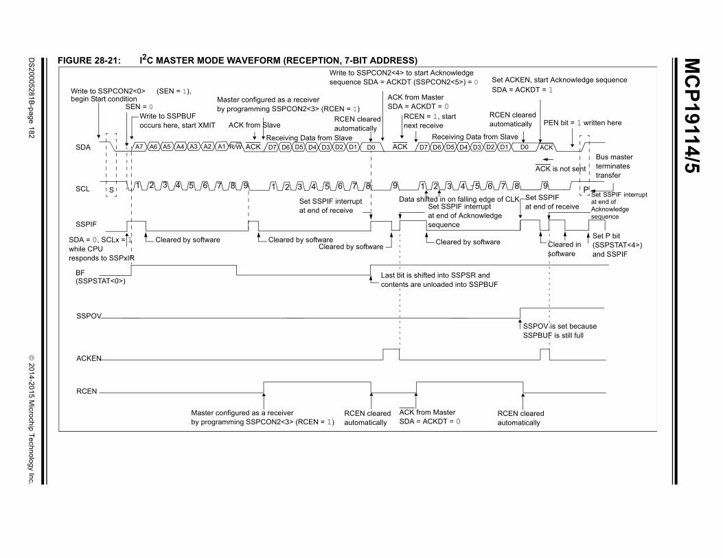
MC
P19114/5
DS
20005281B-page 182
2014-2015 M
icrochip Technology Inc.
P987
D0D1 Slave
ACK is not sent
of CLK
ACK
re
et ACKEN, start Acknowledge sequenceDA = ACKDT = 1
CEN clearedutomatically PEN bit = 1 written here
Bus masterterminatestransfer
ge
Set SSPIFat end of receive
Cleared insoftware
Set SSPIF interruptat end ofAcknowledgesequence
Set P bit(SSPSTAT<4>)and SSPIF
F
SSPOV is set becauseSSPBUF is still full
RCEN clearedautomatically
FIGURE 28-21: I2C MASTER MODE WAVEFORM (RECEPTION, 7-BIT ADDRESS)
65
D2D3D4D5D6D7
S
A7 A6 A5 A4 A3 A2 A1SDA
SCL 1 2 3 4 5 6 7 8 9 1 2 3 4 5 6 7 8 9 1 2 3 4
ACKReceiving Data fromReceiving Data from Slave
D0D1D2D3D4D5D6D7ACKR/W
SSPIF
BF
Write to SSPCON2<0> (SEN = 1),
ACK from Slave
Data shifted in on falling edge
Cleared by software
SEN = 0
SSPOV
(SSPSTAT<0>)
Cleared by softwaCleared by software
ACKEN
begin Start condition
Cleared by software
RCEN
Write to SSPBUFoccurs here, start XMIT
Master configured as a receiverby programming SSPCON2<3> (RCEN = 1)
RCEN clearedautomatically
Write to SSPCON2<4> to start Acknowledgesequence SDA = ACKDT (SSPCON2<5>) = 0
ACK from MasterSDA = ACKDT = 0
RCEN = 1, startnext receive
SS
Ra
SDA = 0, SCLx = 1while CPUresponds to SSPxIR
Set SSPIF interruptat end of receive Set SSPIF interrupt
at end of Acknowledsequence
Last bit is shifted into SSPSR andcontents are unloaded into SSPBU
Master configured as a receiverby programming SSPCON2<3> (RCEN = 1)
RCEN clearedautomatically
ACK from MasterSDA = ACKDT = 0

MCP19114/5
28.5.8 ACKNOWLEDGE SEQUENCETIMINGAn Acknowledge sequence is enabled by setting theAcknowledge Sequence Enable (ACKEN) bit in theSSPCON2 register. When this bit is set, the SCL pin ispulled low and the contents of the Acknowledge data bitare presented on the SDA pin. If the user wishes togenerate an Acknowledge, then the ACKDT bit shouldbe cleared. If not, the user should set the ACKDT bitbefore starting an Acknowledge sequence. The BaudRate Generator then counts for one rollover period(TBRG) and the SCL pin is deasserted (pulled high).When the SCL pin is sampled high (clock arbitration),the Baud Rate Generator counts for TBRG. The SCL pinis then pulled low. Following this, the ACKEN bit isautomatically cleared, the Baud Rate Generator isturned off and the MSSP module then goes into Idlemode (Figure 28-22).
28.5.8.1 WCOL Status FlagIf the user writes the SSPBUF when an Acknowledgesequence is in progress, WCOL is set and the contentsof the buffer are unchanged (the write does not occur).
2014-2015 Microchip Technology Inc.
28.5.9 STOP CONDITION TIMINGA Stop bit is asserted on the SDA pin at the end of areceive/transmit by setting the Stop Sequence Enablebit, PEN, in the SSPCON2 register. At the end of areceive/transmit, the SCL line is held low after thefalling edge of the 9th clock. When the PEN bit is set,the master will assert the SDA line low. When the SDAline is sampled low, the Baud Rate Generator isreloaded and counts down to ‘0’. When the Baud RateGenerator times out, the SCL pin will be brought highand then, one TBRG (Baud Rate Generator rollovercount) later, the SDA pin will be deasserted. When theSDA pin is sampled high while SCL is high, the P bit inthe SSPSTAT register, is set. A TBRG later, the PEN bitis cleared and the SSPIF bit is set (Figure 28-23).
28.5.9.1 WCOL Status FlagIf the user writes the SSPBUF when a Stop sequenceis in progress, the WCOL bit is set and the contents ofthe buffer are unchanged (the write does not occur).
FIGURE 28-22: ACKNOWLEDGE SEQUENCE WAVEFORM
FIGURE 28-23: STOP CONDITION RECEIVE OR TRANSMIT MODE
SDA
SCL
ACKEN automatically cleared
TBRG TBRG
8
D0
9
SSPIF
ACK
Acknowledge sequence starts here,write to SSPCON2
ACKEN = 1, ACKDT = 0
SSPIF set at the endof receive Cleared in
software
Cleared insoftware
SSPIF set at the endof Acknowledge sequenceNote: TBRG = one Baud Rate Generator period.
SCL
SDA
SCL brought high after TBRG
TBRG TBRG
TBRG
ACKP
TBRG
Write to SSPCON2,set PEN
Falling edge of 9th clock
SCL = 1 for TBRG, followed by SDA = 1 for TBRGafter SDA sampled high. P bit (SSPSTAT<4>) is set.
PEN bit (SSPCON2<2>) is cleared byhardware and the SSPIF bit is set
Note: TBRG = one Baud Rate Generator period.
DS20005281B-page 183
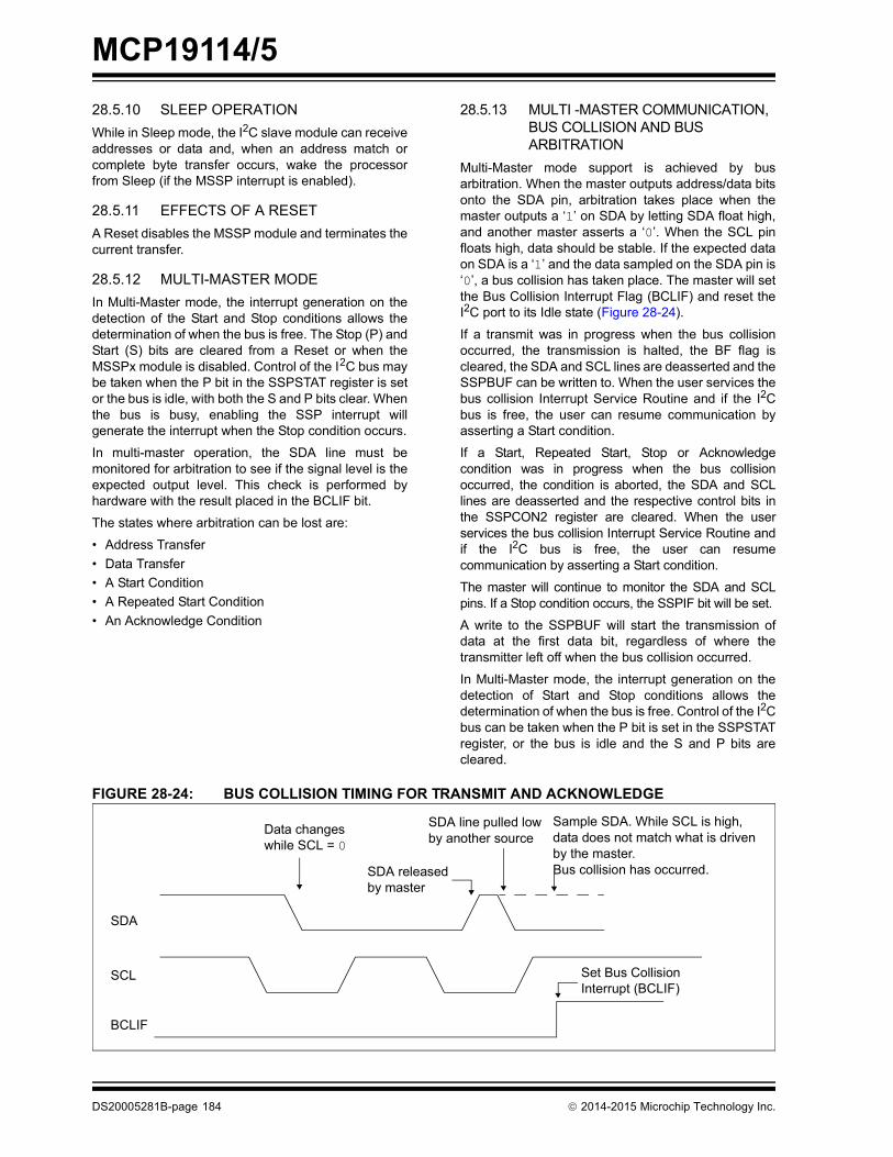
MCP19114/5
28.5.10 SLEEP OPERATIONWhile in Sleep mode, the I2C slave module can receiveaddresses or data and, when an address match orcomplete byte transfer occurs, wake the processorfrom Sleep (if the MSSP interrupt is enabled).28.5.11 EFFECTS OF A RESETA Reset disables the MSSP module and terminates thecurrent transfer.
28.5.12 MULTI-MASTER MODEIn Multi-Master mode, the interrupt generation on thedetection of the Start and Stop conditions allows thedetermination of when the bus is free. The Stop (P) andStart (S) bits are cleared from a Reset or when theMSSPx module is disabled. Control of the I2C bus maybe taken when the P bit in the SSPSTAT register is setor the bus is idle, with both the S and P bits clear. Whenthe bus is busy, enabling the SSP interrupt willgenerate the interrupt when the Stop condition occurs.
In multi-master operation, the SDA line must bemonitored for arbitration to see if the signal level is theexpected output level. This check is performed byhardware with the result placed in the BCLIF bit.
The states where arbitration can be lost are:
• Address Transfer • Data Transfer• A Start Condition• A Repeated Start Condition• An Acknowledge Condition
DS20005281B-page 184
28.5.13 MULTI -MASTER COMMUNICATION, BUS COLLISION AND BUS ARBITRATION
Multi-Master mode support is achieved by busarbitration. When the master outputs address/data bitsonto the SDA pin, arbitration takes place when themaster outputs a ‘1’ on SDA by letting SDA float high,and another master asserts a ‘0’. When the SCL pinfloats high, data should be stable. If the expected dataon SDA is a ‘1’ and the data sampled on the SDA pin is‘0’, a bus collision has taken place. The master will setthe Bus Collision Interrupt Flag (BCLIF) and reset theI2C port to its Idle state (Figure 28-24).
If a transmit was in progress when the bus collisionoccurred, the transmission is halted, the BF flag iscleared, the SDA and SCL lines are deasserted and theSSPBUF can be written to. When the user services thebus collision Interrupt Service Routine and if the I2Cbus is free, the user can resume communication byasserting a Start condition.
If a Start, Repeated Start, Stop or Acknowledgecondition was in progress when the bus collisionoccurred, the condition is aborted, the SDA and SCLlines are deasserted and the respective control bits inthe SSPCON2 register are cleared. When the userservices the bus collision Interrupt Service Routine andif the I2C bus is free, the user can resumecommunication by asserting a Start condition.
The master will continue to monitor the SDA and SCLpins. If a Stop condition occurs, the SSPIF bit will be set.
A write to the SSPBUF will start the transmission ofdata at the first data bit, regardless of where thetransmitter left off when the bus collision occurred.
In Multi-Master mode, the interrupt generation on thedetection of Start and Stop conditions allows thedetermination of when the bus is free. Control of the I2Cbus can be taken when the P bit is set in the SSPSTATregister, or the bus is idle and the S and P bits arecleared.
FIGURE 28-24: BUS COLLISION TIMING FOR TRANSMIT AND ACKNOWLEDGE
SDA
SCL
BCLIF
Data changeswhile SCL = 0
SDA line pulled lowby another source
SDA releasedby master
Sample SDA. While SCL is high,data does not match what is drivenby the master.Bus collision has occurred.
Set Bus CollisionInterrupt (BCLIF)
2014-2015 Microchip Technology Inc.
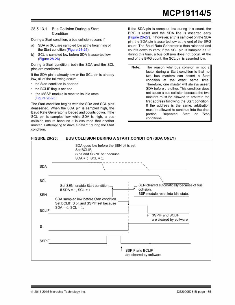
MCP19114/5
28.5.13.1 Bus Collision During a StartConditionDuring a Start condition, a bus collision occurs if:
a) SDA or SCL are sampled low at the beginning ofthe Start condition (Figure 28-25)
b) SCL is sampled low before SDA is asserted low(Figure 28-26)
During a Start condition, both the SDA and the SCLpins are monitored.
If the SDA pin is already low or the SCL pin is alreadylow, all of the following occur:• the Start condition is aborted• the BCLIF flag is set and• the MSSP module is reset to its Idle state
(Figure 28-25)
The Start condition begins with the SDA and SCL pinsdeasserted. When the SDA pin is sampled high, theBaud Rate Generator is loaded and counts down. If theSCL pin is sampled low while SDA is high, a buscollision occurs because it is assumed that anothermaster is attempting to drive a data ‘1’ during the Startcondition.
2014-2015 Microchip Technology Inc.
If the SDA pin is sampled low during this count, theBRG is reset and the SDA line is asserted early(Figure 28-27). If, however, a ‘1’ is sampled on the SDApin, the SDA pin is asserted low at the end of the BRGcount. The Baud Rate Generator is then reloaded andcounts down to zero; if the SCL pin is sampled as ‘0’during this time, a bus collision does not occur. At theend of the BRG count, the SCL pin is asserted low.
Note: The reason why bus collision is not afactor during a Start condition is that notwo bus masters can assert a Startcondition at the exact same time.Therefore, one master will always assertSDA before the other. This condition doesnot cause a bus collision because the twomasters must be allowed to arbitrate thefirst address following the Start condition.If the address is the same, arbitrationmust be allowed to continue into the dataportion, Repeated Start or Stopconditions.
FIGURE 28-25: BUS COLLISION DURING A START CONDITION (SDA ONLY)
SDA
SCL
SEN
BCLIF
S
SSPIF
SDA goes low before the SEN bit is set.Set BCLIF,S bit and SSPIF set becauseSDA = 0, SCL = 1.
Set SEN, enable Start conditionif SDA = 1, SCL = 1
SEN cleared automatically because of buscollision.SSP module reset into Idle state.
SDA sampled low before Start condition.Set BCLIF. S bit and SSPIF set because SDA = 0, SCL = 1.
SSPIF and BCLIFare cleared by software
SSPIF and BCLIFare cleared by software
DS20005281B-page 185

MCP19114/5
FIGURE 28-26: BUS COLLISION DURING A START CONDITION (SCL = 0)FIGURE 28-27: BRG RESET DUE TO SDA ARBITRATION DURING START CONDITION
SDA
SCL
SEN
TBRG TBRG
SDA = 0, SCL = 1
BCLIF
S
SSPIF
‘0’
Set SEN, enable Startsequence if SDA = 1, SCL = 1
SCL = 0 before SDA = 0,
bus collision occurs. Set BCLIF.SCL = 0 before BRG time out,bus collision occurs. Set BCLIF.
Interrupt clearedby software
‘0’
‘0’
‘0’
SDA
SCL
SEN
Set SLess than Tbrg TBRG
SDA = 0, SCL = 1
BCLIF
S
SSPIF
s
Set SSPIF
‘0’
SDA pulled low by other master.Reset BRG and assert SDAx.
SCLx pulled low after BRGtime out
Set SEN, enable Startsequence if SDA = 1, SCL = 1
SDAx = 0, SCL = 1,set SSPIF
Interrupts clearedby software
DS20005281B-page 1
86 2014-2015 Microchip Technology Inc.
MCP19114/5
28.5.13.2 Bus Collision During a RepeatedStart ConditionDuring a Repeated Start condition, a bus collisionoccurs if:
a) A low level is sampled on SDA when SCL goesfrom low level to high level
b) SCL goes low before SDA is asserted low,indicating that another master is attempting totransmit a data ‘1’
When the user releases SDA and the pin is allowed tofloat high, the BRG is loaded with SSPADD and countsdown to zero. The SCL pin is then deasserted and,when sampled high, the SDA pin is sampled.
2014-2015 Microchip Technology Inc.
If SDA is low, a bus collision has occurred (i.e., anothermaster is attempting to transmit a data ‘0’, Figure 28-28).If SDA is sampled high, the BRG is reloaded and beginscounting. If SDA goes from high to low before the BRGtimes out, no bus collision occurs because no twomasters can assert SDA at exactly the same time.
If SCL goes from high to low before the BRG times outand SDA has not already been asserted, a bus collisionoccurs. In this case, another master is attempting totransmit a data ‘1’ during the Repeated Start condition(refer to Figure 28-29).
If, at the end of the BRG time out, both SCL and SDA arestill high, the SDA pin is driven low and the BRG isreloaded and begins counting. At the end of the count,regardless of the status of the SCL pin, the SCL pin isdriven low and the Repeated Start condition is complete.
FIGURE 28-28: BUS COLLISION DURING A REPEATED START CONDITION (CASE 1)
FIGURE 28-29: BUS COLLISION DURING A REPEATED START CONDITION (CASE 2)
SDA
SCL
RSEN
BCLIF
S
SSPIF
Cleared by software
‘0’
‘0’
Sample SDA when SCL goes high.If SDA = 0, set BCLIF and release SDA and SCL.
SDA
SCL
BCLIF
RSEN
S
SSPIF
TBRG TBRG
‘0’
SCL goes low before SDA,set BCLIF. Release SDA and SCL.
Interrupt clearedby software
‘0’
DS20005281B-page 187
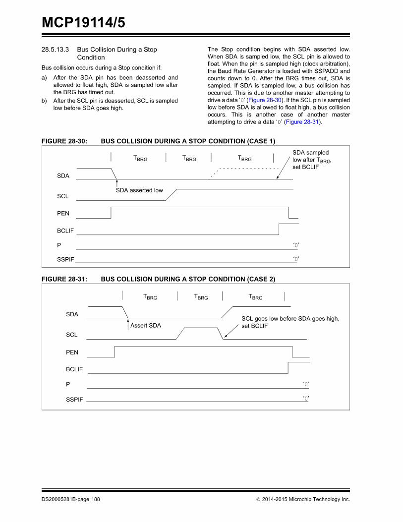
MCP19114/5
28.5.13.3 Bus Collision During a StopConditionBus collision occurs during a Stop condition if:
a) After the SDA pin has been deasserted andallowed to float high, SDA is sampled low afterthe BRG has timed out.
b) After the SCL pin is deasserted, SCL is sampledlow before SDA goes high.
DS20005281B-page 188
The Stop condition begins with SDA asserted low.When SDA is sampled low, the SCL pin is allowed tofloat. When the pin is sampled high (clock arbitration),the Baud Rate Generator is loaded with SSPADD andcounts down to 0. After the BRG times out, SDA issampled. If SDA is sampled low, a bus collision hasoccurred. This is due to another master attempting todrive a data ‘0’ (Figure 28-30). If the SCL pin is sampledlow before SDA is allowed to float high, a bus collisionoccurs. This is another case of another masterattempting to drive a data ‘0’ (Figure 28-31).
FIGURE 28-30: BUS COLLISION DURING A STOP CONDITION (CASE 1)
FIGURE 28-31: BUS COLLISION DURING A STOP CONDITION (CASE 2)
SDA
SCL
BCLIF
PEN
P
SSPIF
TBRG TBRG TBRG
SDA asserted low
‘0’
‘0’
SDA sampledlow after TBRG,set BCLIF
SDA
SCL
BCLIF
PEN
P
SSPIF
TBRG TBRG TBRG
Assert SDA
‘0’
‘0’
SCL goes low before SDA goes high,set BCLIF
2014-2015
Microchip Technology Inc.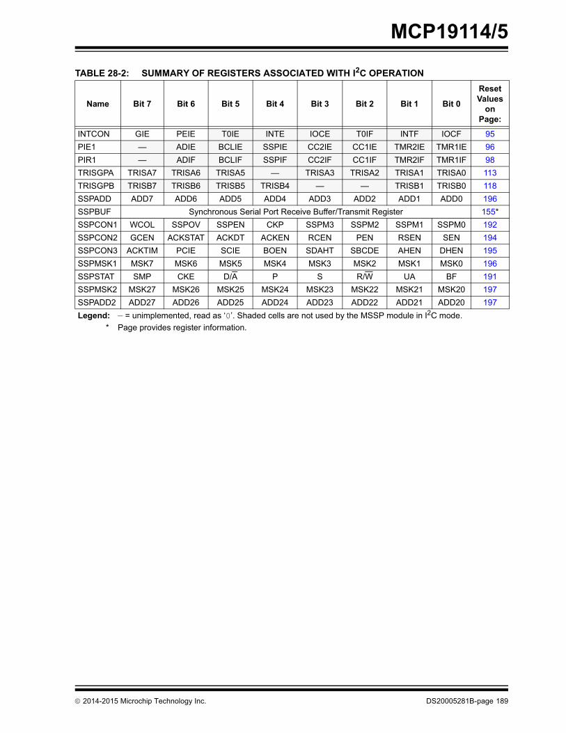
MCP19114/5
TABLE 28-2: SUMMARY OF REGISTERS ASSOCIATED WITH I2C OPERATION
Name Bit 7 Bit 6 Bit 5 Bit 4 Bit 3 Bit 2 Bit 1 Bit 0
Reset Values
on Page:
INTCON GIE PEIE T0IE INTE IOCE T0IF INTF IOCF 95PIE1 — ADIE BCLIE SSPIE CC2IE CC1IE TMR2IE TMR1IE 96PIR1 — ADIF BCLIF SSPIF CC2IF CC1IF TMR2IF TMR1IF 98TRISGPA TRISA7 TRISA6 TRISA5 — TRISA3 TRISA2 TRISA1 TRISA0 113TRISGPB TRISB7 TRISB6 TRISB5 TRISB4 — — TRISB1 TRISB0 118SSPADD ADD7 ADD6 ADD5 ADD4 ADD3 ADD2 ADD1 ADD0 196SSPBUF Synchronous Serial Port Receive Buffer/Transmit Register 155*SSPCON1 WCOL SSPOV SSPEN CKP SSPM3 SSPM2 SSPM1 SSPM0 192SSPCON2 GCEN ACKSTAT ACKDT ACKEN RCEN PEN RSEN SEN 194SSPCON3 ACKTIM PCIE SCIE BOEN SDAHT SBCDE AHEN DHEN 195SSPMSK1 MSK7 MSK6 MSK5 MSK4 MSK3 MSK2 MSK1 MSK0 196SSPSTAT SMP CKE D/A P S R/W UA BF 191SSPMSK2 MSK27 MSK26 MSK25 MSK24 MSK23 MSK22 MSK21 MSK20 197SSPADD2 ADD27 ADD26 ADD25 ADD24 ADD23 ADD22 ADD21 ADD20 197Legend: — = unimplemented, read as ‘0’. Shaded cells are not used by the MSSP module in I2C mode.
* Page provides register information.
2014-2015 Microchip Technology Inc. DS20005281B-page 189
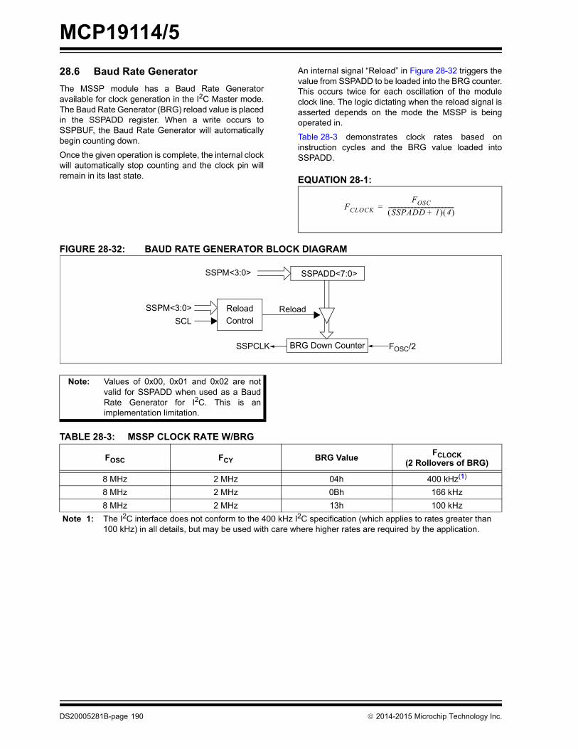
MCP19114/5
28.6 Baud Rate GeneratorThe MSSP module has a Baud Rate Generatoravailable for clock generation in the I2C Master mode.The Baud Rate Generator (BRG) reload value is placedin the SSPADD register. When a write occurs toSSPBUF, the Baud Rate Generator will automaticallybegin counting down.Once the given operation is complete, the internal clockwill automatically stop counting and the clock pin willremain in its last state.
DS20005281B-page 190
An internal signal “Reload” in Figure 28-32 triggers thevalue from SSPADD to be loaded into the BRG counter.This occurs twice for each oscillation of the moduleclock line. The logic dictating when the reload signal isasserted depends on the mode the MSSP is beingoperated in.
Table 28-3 demonstrates clock rates based oninstruction cycles and the BRG value loaded intoSSPADD.
EQUATION 28-1:
FCLOCKFOSC
SSPADD 1+ 4 ----------------------------------------------=
FIGURE 28-32: BAUD RATE GENERATOR BLOCK DIAGRAM
Note: Values of 0x00, 0x01 and 0x02 are notvalid for SSPADD when used as a BaudRate Generator for I2C. This is animplementation limitation.
TABLE 28-3: MSSP CLOCK RATE W/BRG
FOSC FCY BRG Value FCLOCK (2 Rollovers of BRG)
8 MHz 2 MHz 04h 400 kHz(1)
8 MHz 2 MHz 0Bh 166 kHz8 MHz 2 MHz 13h 100 kHz
Note 1: The I2C interface does not conform to the 400 kHz I2C specification (which applies to rates greater than 100 kHz) in all details, but may be used with care where higher rates are required by the application.
SSPM<3:0>
BRG Down CounterSSPCLK FOSC/2
SSPADD<7:0>
SSPM<3:0>SCL
ReloadControl
Reload
2014-2015 Microchip Technology Inc.
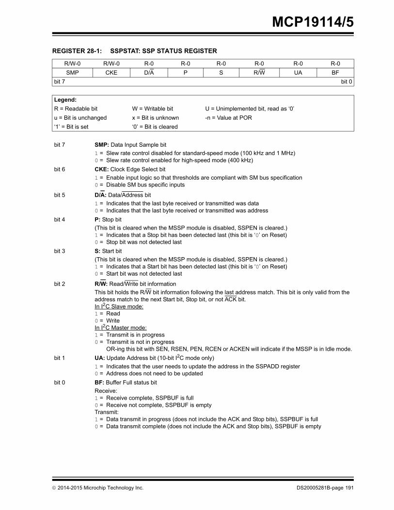
MCP19114/5
REGISTER 28-1: SSPSTAT: SSP STATUS REGISTER
R/W-0 R/W-0 R-0 R-0 R-0 R-0 R-0 R-0SMP CKE D/A P S R/W UA BF
bit 7 bit 0
Legend:R = Readable bit W = Writable bit U = Unimplemented bit, read as ‘0’u = Bit is unchanged x = Bit is unknown -n = Value at POR‘1’ = Bit is set ‘0’ = Bit is cleared
bit 7 SMP: Data Input Sample bit1 = Slew rate control disabled for standard-speed mode (100 kHz and 1 MHz)0 = Slew rate control enabled for high-speed mode (400 kHz)
bit 6 CKE: Clock Edge Select bit1 = Enable input logic so that thresholds are compliant with SM bus specification0 = Disable SM bus specific inputs
bit 5 D/A: Data/Address bit1 = Indicates that the last byte received or transmitted was data0 = Indicates that the last byte received or transmitted was address
bit 4 P: Stop bit(This bit is cleared when the MSSP module is disabled, SSPEN is cleared.)1 = Indicates that a Stop bit has been detected last (this bit is ‘0’ on Reset)0 = Stop bit was not detected last
bit 3 S: Start bit(This bit is cleared when the MSSP module is disabled, SSPEN is cleared.)1 = Indicates that a Start bit has been detected last (this bit is ‘0’ on Reset)0 = Start bit was not detected last
bit 2 R/W: Read/Write bit informationThis bit holds the R/W bit information following the last address match. This bit is only valid from theaddress match to the next Start bit, Stop bit, or not ACK bit.In I2 C Slave mode:1 = Read0 = WriteIn I2 C Master mode:1 = Transmit is in progress0 = Transmit is not in progress
OR-ing this bit with SEN, RSEN, PEN, RCEN or ACKEN will indicate if the MSSP is in Idle mode.bit 1 UA: Update Address bit (10-bit I2C mode only)
1 = Indicates that the user needs to update the address in the SSPADD register0 = Address does not need to be updated
bit 0 BF: Buffer Full status bitReceive:1 = Receive complete, SSPBUF is full0 = Receive not complete, SSPBUF is emptyTransmit:1 = Data transmit in progress (does not include the ACK and Stop bits), SSPBUF is full0 = Data transmit complete (does not include the ACK and Stop bits), SSPBUF is empty
2014-2015 Microchip Technology Inc. DS20005281B-page 191

MCP19114/5
REGISTER 28-2: SSPCON1: SSP CONTROL REGISTER 1R/C/HS-0 R/C/HS-0 R/W-0 R/W-0 R/W-0 R/W-0 R/W-0 R/W-0WCOL SSPOV SSPEN CKP SSPM<3:0>
bit 7 bit 0
Legend:R = Readable bit W = Writable bit U = Unimplemented bit, read as ‘0’u = Bit is unchanged x = Bit is unknown -n = Value at POR‘1’ = Bit is set ‘0’ = Bit is cleared HS = Bit is set by hardware C = User cleared
bit 7 WCOL: Write Collision Detect bitMaster mode:1 = A write to the SSPBUF register was attempted while the I2C conditions were not valid for a
transmission to be started0 = No collisionSlave mode:1 = The SSPBUF register is written while it is still transmitting the previous word (must be cleared in
software)0 = No collision
bit 6 SSPOV: Receive Overflow Indicator bit(1)
1 = A byte is received while the SSPBUF register is still holding the previous byte. SSPOV is a “don’tcare” in Transmit mode (must be cleared in software).
0 = No overflowbit 5 SSPEN: Synchronous Serial Port Enable bit
In both modes, when enabled, these pins must be properly configured as input or output1 = Enables the serial port and configures the SDA and SCL pins as the source of the serial port
pins(2)
0 = Disables serial port and configures these pins as I/O port pinsbit 4 CKP: Clock Polarity Select bit
In I2 C Slave mode:SCL release control1 = Enable clock0 = Holds clock low (clock stretch). (Used to ensure data setup time.)In I2 C Master mode:Unused in this mode
Note 1: In Master mode, the overflow bit is not set since each new reception (and transmission) is initiated by writing to the SSPBUF register.
2: When enabled, the SDA and SCL pins must be configured as inputs.3: SSPADD values of 0, 1 or 2 are not supported for I2C mode.
DS20005281B-page 192 2014-2015 Microchip Technology Inc.
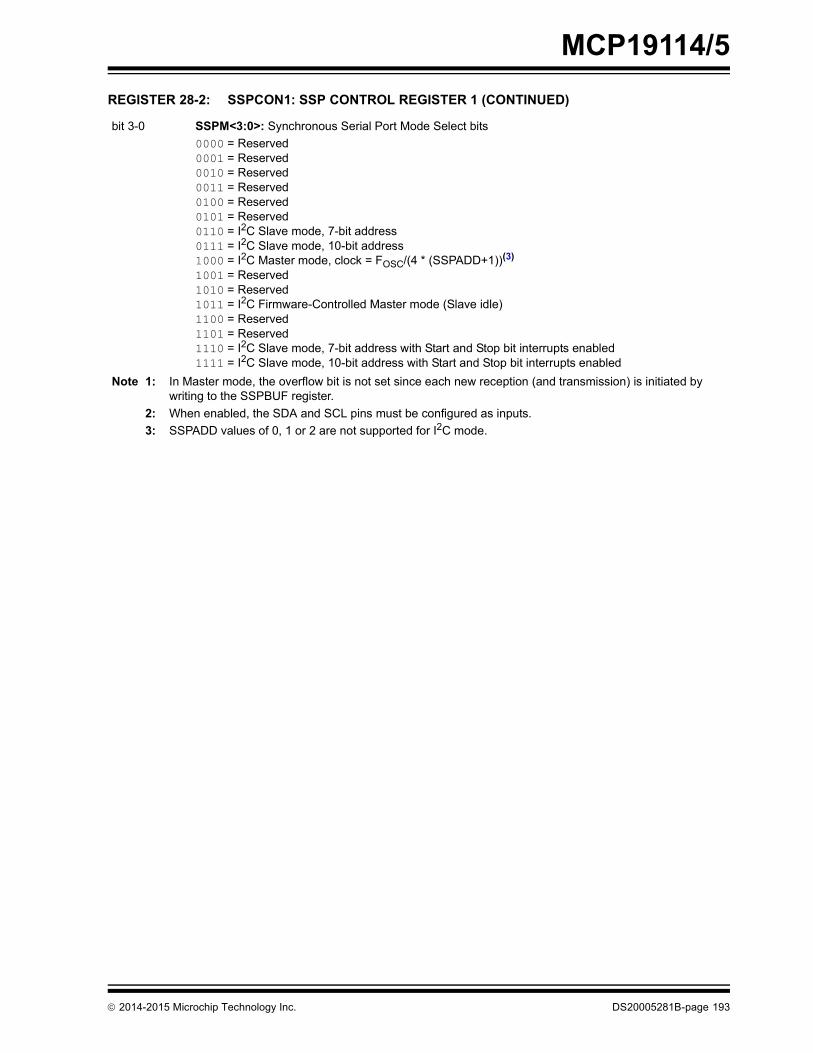
MCP19114/5
bit 3-0 SSPM<3:0>: Synchronous Serial Port Mode Select bits0000 = Reserved0001 = Reserved0010 = Reserved 0011 = Reserved 0100 = Reserved0101 = Reserved0110 = I2C Slave mode, 7-bit address 0111 = I2C Slave mode, 10-bit address 1000 = I2C Master mode, clock = FOSC/(4 * (SSPADD+1))(3)
1001 = Reserved1010 = Reserved1011 = I2C Firmware-Controlled Master mode (Slave idle) 1100 = Reserved 1101 = Reserved 1110 = I2C Slave mode, 7-bit address with Start and Stop bit interrupts enabled 1111 = I2C Slave mode, 10-bit address with Start and Stop bit interrupts enabled
REGISTER 28-2: SSPCON1: SSP CONTROL REGISTER 1 (CONTINUED)
Note 1: In Master mode, the overflow bit is not set since each new reception (and transmission) is initiated by writing to the SSPBUF register.
2: When enabled, the SDA and SCL pins must be configured as inputs.3: SSPADD values of 0, 1 or 2 are not supported for I2C mode.
2014-2015 Microchip Technology Inc. DS20005281B-page 193

MCP19114/5
REGISTER 28-3: SSPCON2: SSP CONTROL REGISTER 2
R/W-0/0 R-0/0 R/W-0/0 R/S/HS-0/0 R/S/HS-0/0 R/S/HS-0/0 R/S/HS-0/0 R/W/HS-0/0GCEN ACKSTAT ACKDT ACKEN RCEN PEN RSEN SEN
bit 7 bit 0
Legend:R = Readable bit W = Writable bit U = Unimplemented bit, read as ‘0’u = Bit is unchanged x = Bit is unknown -n/n = Value at POR and BOR/Value at all other Resets‘1’ = Bit is set ‘0’ = Bit is cleared H = Bit is set by hardware S = User set
bit 7 GCEN: General Call Enable bit (in I2C Slave mode only)1 = Enable interrupt when a general call address (0x00 or 00h) is received in the SSPSR register0 = General call address disabled
bit 6 ACKSTAT: Acknowledge Status bit (in I2C mode only)1 = Acknowledge was not received0 = Acknowledge was received
bit 5 ACKDT: Acknowledge Data bit (in I2C mode only)In Receive mode:Value transmitted when the user initiates an Acknowledge sequence at the end of a receive1 = Not Acknowledge0 = Acknowledge
bit 4 ACKEN: Acknowledge Sequence Enable bit (in I2C Master mode only)In Master Receive mode:1 = Initiate Acknowledge sequence on SDA and SCL pins and transmit ACKDT data bit. Automatically
cleared by hardware.0 = Acknowledge sequence idle
bit 3 RCEN: Receive Enable bit (in I2C Master mode only)1 = Enables Receive mode for I2C0 = Receive idle
bit 2 PEN: Stop Condition Enable bit (in I2C Master mode only)SCK Release Control:1 = Initiate Stop condition on SDA and SCL pins. Automatically cleared by hardware.0 = Stop condition idle
bit 1 RSEN: Repeated Start Condition Enabled bit (in I2C Master mode only)1 = Initiate Repeated Start condition on SDA and SCL pins. Automatically cleared by hardware.0 = Repeated Start condition idle
bit 0 SEN: Start Condition Enabled bit (in I2C Master mode only)In Master mode:1 = Initiate Start condition on SDA and SCL pins. Automatically cleared by hardware.0 = Start condition idleIn Slave mode:1 = Clock stretching is enabled for both Slave Transmit and Slave Receive (stretch enabled)0 = Clock stretching is disabled
Note 1: For bits ACKEN, RCEN, PEN, RSEN, SEN: If the I2C module is not in the Idle mode, this bit may not be set (no spooling) and the SSPBUF may not be written (or writes to the SSPBUF are disabled).
DS20005281B-page 194 2014-2015 Microchip Technology Inc.
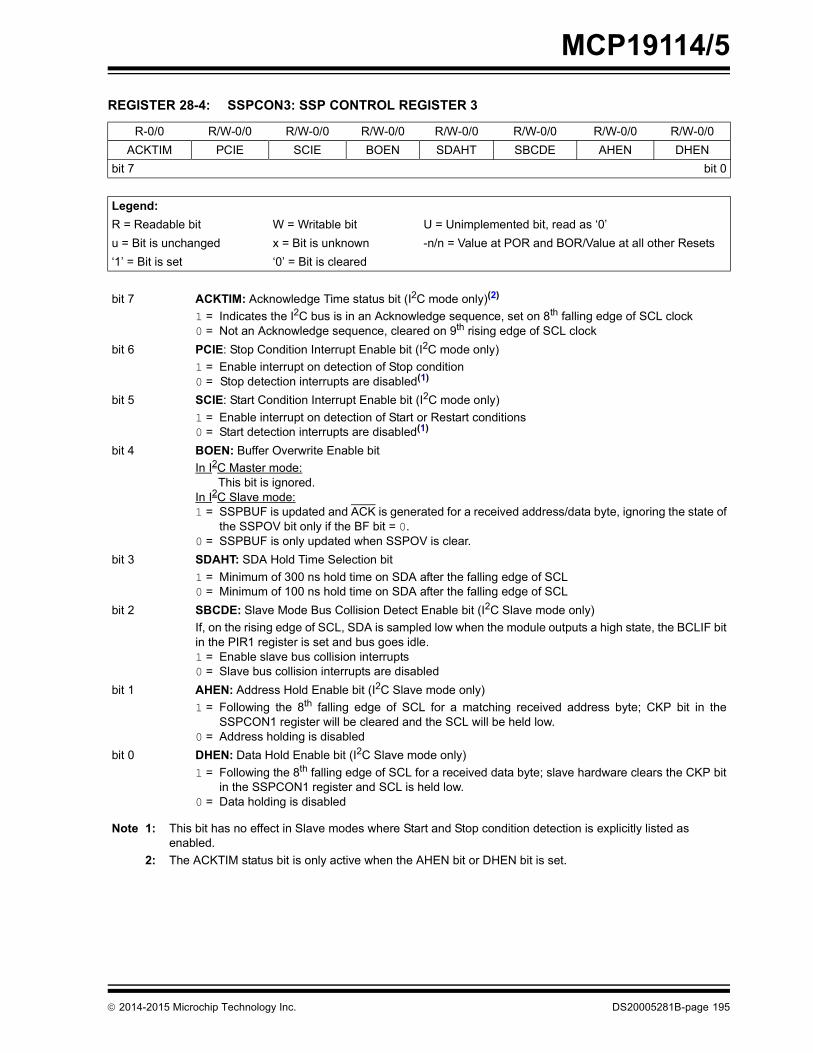
MCP19114/5
REGISTER 28-4: SSPCON3: SSP CONTROL REGISTER 3
R-0/0 R/W-0/0 R/W-0/0 R/W-0/0 R/W-0/0 R/W-0/0 R/W-0/0 R/W-0/0ACKTIM PCIE SCIE BOEN SDAHT SBCDE AHEN DHEN
bit 7 bit 0
Legend:R = Readable bit W = Writable bit U = Unimplemented bit, read as ‘0’u = Bit is unchanged x = Bit is unknown -n/n = Value at POR and BOR/Value at all other Resets‘1’ = Bit is set ‘0’ = Bit is cleared
bit 7 ACKTIM: Acknowledge Time status bit (I2C mode only)(2)
1 = Indicates the I2C bus is in an Acknowledge sequence, set on 8th falling edge of SCL clock0 = Not an Acknowledge sequence, cleared on 9th rising edge of SCL clock
bit 6 PCIE: Stop Condition Interrupt Enable bit (I2C mode only)1 = Enable interrupt on detection of Stop condition0 = Stop detection interrupts are disabled(1)
bit 5 SCIE: Start Condition Interrupt Enable bit (I2C mode only)1 = Enable interrupt on detection of Start or Restart conditions0 = Start detection interrupts are disabled(1)
bit 4 BOEN: Buffer Overwrite Enable bitIn I2C Master mode:
This bit is ignored.In I2C Slave mode:1 = SSPBUF is updated and ACK is generated for a received address/data byte, ignoring the state of
the SSPOV bit only if the BF bit = 0.0 = SSPBUF is only updated when SSPOV is clear.
bit 3 SDAHT: SDA Hold Time Selection bit1 = Minimum of 300 ns hold time on SDA after the falling edge of SCL0 = Minimum of 100 ns hold time on SDA after the falling edge of SCL
bit 2 SBCDE: Slave Mode Bus Collision Detect Enable bit (I2C Slave mode only)If, on the rising edge of SCL, SDA is sampled low when the module outputs a high state, the BCLIF bitin the PIR1 register is set and bus goes idle.1 = Enable slave bus collision interrupts0 = Slave bus collision interrupts are disabled
bit 1 AHEN: Address Hold Enable bit (I2C Slave mode only)1 = Following the 8th falling edge of SCL for a matching received address byte; CKP bit in the
SSPCON1 register will be cleared and the SCL will be held low.0 = Address holding is disabled
bit 0 DHEN: Data Hold Enable bit (I2C Slave mode only)1 = Following the 8th falling edge of SCL for a received data byte; slave hardware clears the CKP bit
in the SSPCON1 register and SCL is held low.0 = Data holding is disabled
Note 1: This bit has no effect in Slave modes where Start and Stop condition detection is explicitly listed as enabled.
2: The ACKTIM status bit is only active when the AHEN bit or DHEN bit is set.
2014-2015 Microchip Technology Inc. DS20005281B-page 195
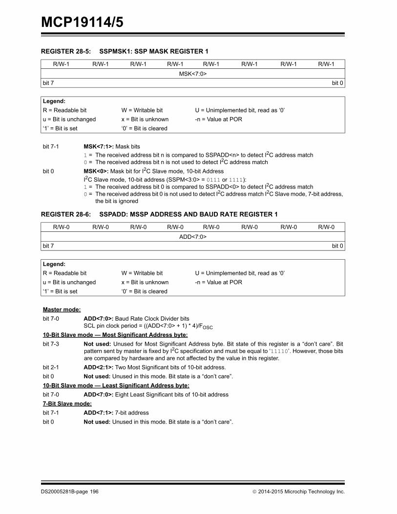
MCP19114/5
REGISTER 28-5: SSPMSK1: SSP MASK REGISTER 1
R/W-1 R/W-1 R/W-1 R/W-1 R/W-1 R/W-1 R/W-1 R/W-1
MSK<7:0>bit 7 bit 0
Legend:R = Readable bit W = Writable bit U = Unimplemented bit, read as ‘0’u = Bit is unchanged x = Bit is unknown -n = Value at POR‘1’ = Bit is set ‘0’ = Bit is cleared
bit 7-1 MSK<7:1>: Mask bits1 = The received address bit n is compared to SSPADD<n> to detect I2C address match0 = The received address bit n is not used to detect I2C address match
bit 0 MSK<0>: Mask bit for I2C Slave mode, 10-bit AddressI2C Slave mode, 10-bit address (SSPM<3:0> = 0111 or 1111):1 = The received address bit 0 is compared to SSPADD<0> to detect I2C address match0 = The received address bit 0 is not used to detect I2C address match I2C Slave mode, 7-bit address,
the bit is ignored
REGISTER 28-6: SSPADD: MSSP ADDRESS AND BAUD RATE REGISTER 1
R/W-0 R/W-0 R/W-0 R/W-0 R/W-0 R/W-0 R/W-0 R/W-0
ADD<7:0>bit 7 bit 0
Legend:R = Readable bit W = Writable bit U = Unimplemented bit, read as ‘0’u = Bit is unchanged x = Bit is unknown -n = Value at POR‘1’ = Bit is set ‘0’ = Bit is cleared
Master mode:bit 7-0 ADD<7:0>: Baud Rate Clock Divider bits
SCL pin clock period = ((ADD<7:0> + 1) * 4)/FOSC10-Bit Slave mode — Most Significant Address byte:bit 7-3 Not used: Unused for Most Significant Address byte. Bit state of this register is a “don’t care”. Bit
pattern sent by master is fixed by I2C specification and must be equal to ‘11110’. However, those bitsare compared by hardware and are not affected by the value in this register.
bit 2-1 ADD<2:1>: Two Most Significant bits of 10-bit address.bit 0 Not used: Unused in this mode. Bit state is a “don’t care”.10-Bit Slave mode — Least Significant Address byte:bit 7-0 ADD<7:0>: Eight Least Significant bits of 10-bit address7-Bit Slave mode:bit 7-1 ADD<7:1>: 7-bit addressbit 0 Not used: Unused in this mode. Bit state is a “don’t care”.
DS20005281B-page 196 2014-2015 Microchip Technology Inc.

MCP19114/5
REGISTER 28-7: SSPMSK2: SSP MASK REGISTER 2
R/W-1 R/W-1 R/W-1 R/W-1 R/W-1 R/W-1 R/W-1 R/W-1
MSK2<7:0>bit 7 bit 0
Legend:R = Readable bit W = Writable bit U = Unimplemented bit, read as ‘0’u = Bit is unchanged x = Bit is unknown -n = Value at POR‘1’ = Bit is set ‘0’ = Bit is cleared
bit 7-1 MSK2<7:1>: Mask bits1 = The received address bit n is compared to SSPADD2<n> to detect I2C address match0 = The received address bit n is not used to detect I2C address match
bit 0 MSK2<0>: Mask bit for I2C Slave mode, 10-bit AddressI2C Slave mode, 10-bit address (SSPM<3:0> = 0111 or 1111):1 = The received address bit 0 is compared to SSPADD2<0> to detect I2C address match0 = The received address bit 0 is not used to detect I2C address match I2C Slave mode, 7-bit address,
the bit is ignored
REGISTER 28-8: SSPADD2: MSSP ADDRESS 2
R/W-0 R/W-0 R/W-0 R/W-0 R/W-0 R/W-0 R/W-0 R/W-0
ADD2<7:0>bit 7 bit 0
Legend:R = Readable bit W = Writable bit U = Unimplemented bit, read as ‘0’u = Bit is unchanged x = Bit is unknown -n = Value at POR‘1’ = Bit is set ‘0’ = Bit is cleared
Master mode:
bit 7-0 ADD2<7:0>: Baud Rate Clock Divider bitsSCL pin clock period = ((ADD<7:0> + 1) * 4)/FOSC
10-Bit Slave mode — Most Significant Address byte:
bit 7-3 Not used: Unused for Most Significant Address byte. Bit state of this register is a “don’t care”. Bitpattern sent by master is fixed by I2C specification and must be equal to ‘11110’. However, those bitsare compared by hardware and are not affected by the value in this register.
bit 2-1 ADD2<2:1>: Two Most Significant bits of 10-bit addressbit 0 Not used: Unused in this mode. Bit state is a “don’t care”.
10-Bit Slave mode — Least Significant Address byte:
bit 7-0 ADD2<7:0>: Eight Least Significant bits of 10-bit address
7-Bit Slave mode:
bit 7-1 ADD2<7:1>: 7-bit addressbit 0 Not used: Unused in this mode. Bit state is a “don’t care”.
2014-2015 Microchip Technology Inc. DS20005281B-page 197

MCP19114/5
NOTES:DS20005281B-page 198
2014-2015 Microchip Technology Inc.
MCP19114/5
29.0 INSTRUCTION SET SUMMARYThe MCP19114/5 instruction set is highly orthogonaland is comprised of three basic categories:
• Byte-oriented operations• Bit-oriented operations• Literal and control operations
Each instruction is a 14-bit word divided into anopcode, which specifies the instruction type, and oneor more operands, which further specify the operationof the instruction. The formats for each of thecategories is presented in Figure 29-1, while thevarious opcode fields are summarized in Table 29-1.
Table 29-2 lists the instructions recognized by theMPASMTM assembler.
For byte-oriented instructions, ‘f’ represents a fileregister designator and ‘d’ represents a destinationdesignator. The file register designator specifies whichfile register is to be used by the instruction.
The destination designator specifies where the result ofthe operation is to be placed. If ‘d’ is zero, the result isplaced in the W register. If ‘d’ is one, the result is placedin the file register specified in the instruction.
For bit-oriented instructions, ‘b’ represents a bit fielddesignator, which selects the bit affected by theoperation, while ‘f’ represents the address of the file inwhich the bit is located.
For literal and control operations, ‘k’ represents an8-bit or 11-bit constant, or literal value.
One instruction cycle consists of four oscillator periods;for an oscillator frequency of 4 MHz, this gives a normalinstruction execution time of 1 µs. All instructions areexecuted within a single instruction cycle, unless aconditional test is true, or the program counter ischanged as a result of an instruction. When this occurs,the execution takes two instruction cycles, with thesecond cycle executed as an NOP.
All instruction examples use the format ‘0xhh’ torepresent a hexadecimal number, where ‘h’ signifies ahexadecimal digit.
29.1 Read-Modify-Write OperationsAny instruction that specifies a file register as part ofthe instruction performs a Read-Modify-Write (RMW)operation. The register is read, the data is modified,and the result is stored according to either theinstruction or the destination designator ‘d’. A readoperation is performed on a register even if theinstruction writes to that register.
For example, a CLRF PORTA instruction will readPORTGPA, clear all the data bits, then write the resultback to PORTGPA. This example would have theunintended consequence of clearing the condition thatsets the IOCIF flag.
2014-2015 Microchip Technology Inc.
FIGURE 29-1: GENERAL FORMAT FOR INSTRUCTIONS
TABLE 29-1: OPCODE FIELD DESCRIPTIONS
Field Description
f Register file address (0x00 to 0x7F)W Working register (accumulator)b Bit address within an 8-bit file registerk Literal field, constant data or labelx Don’t care location (= 0 or 1).
The assembler will generate code with x = 0. It is the recommended form of use for compatibility with all Microchip software tools.
d Destination select; d = 0: store result in W,d = 1: store result in file register f. Default is d = 1.
PC Program Counter
TO Time-Out bitC Carry bit
DC Digit carry bitZ Zero bit
PD Power-down bit
Byte-oriented file register operations13 8 7 6 0
d = 0 for destination W
OPCODE d f (FILE #)
d = 1 for destination ff = 7-bit file register address
Bit-oriented file register operations13 10 9 7 6 0
OPCODE b (BIT #) f (FILE #)
b = 3-bit bit addressf = 7-bit file register address
Literal and control operations
13 8 7 0OPCODE k (literal)
k = 8-bit immediate value
13 11 10 0OPCODE k (literal)
k = 11-bit immediate value
General
CALL and GOTO instructions only
DS20005281B-page 199
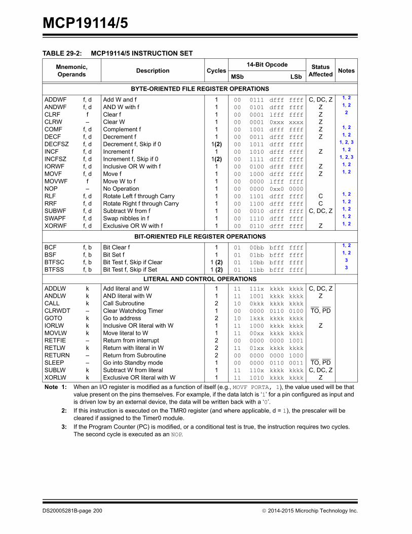
MCP19114/5
TABLE 29-2: MCP19114/5 INSTRUCTION SET
Mnemonic,Operands Description Cycles
14-Bit Opcode StatusAffected Notes
MSb LSb
BYTE-ORIENTED FILE REGISTER OPERATIONS
ADDWFANDWFCLRFCLRWCOMFDECFDECFSZINCFINCFSZIORWFMOVFMOVWFNOPRLFRRFSUBWFSWAPFXORWF
f, df, d
f–
f, df, df, df, df, df, df, d
f–
f, df, df, df, df, d
Add W and fAND W with fClear fClear WComplement fDecrement fDecrement f, Skip if 0Increment fIncrement f, Skip if 0Inclusive OR W with fMove fMove W to fNo OperationRotate Left f through CarryRotate Right f through CarrySubtract W from fSwap nibbles in fExclusive OR W with f
111111
1(2)1
1(2)111111111
000000000000000000000000000000000000
011101010001000110010011101110101111010010000000000011011100001011100110
dfffdffflfff0xxxdfffdfffdfffdfffdfffdfffdffflfff0xx0dfffdfffdfffdfffdfff
ffffffffffffxxxxffffffffffffffffffffffffffffffff0000ffffffffffffffffffff
C, DC, ZZZZZZ
Z
ZZ
CC
C, DC, Z
Z
1, 21, 2
2
1, 21, 2
1, 2, 31, 2
1, 2, 31, 21, 2
1, 21, 21, 21, 21, 2
BIT-ORIENTED FILE REGISTER OPERATIONS
BCFBSFBTFSCBTFSS
f, bf, bf, bf, b
Bit Clear fBit Set fBit Test f, Skip if ClearBit Test f, Skip if Set
11
1 (2)1 (2)
01010101
00bb01bb10bb11bb
bfffbfffbfffbfff
ffffffffffffffff
1, 21, 2
33
LITERAL AND CONTROL OPERATIONSADDLWANDLWCALLCLRWDTGOTOIORLWMOVLWRETFIERETLWRETURNSLEEPSUBLWXORLW
kkk–kkk–k––kk
Add literal and WAND literal with WCall SubroutineClear Watchdog TimerGo to addressInclusive OR literal with WMove literal to WReturn from interruptReturn with literal in WReturn from SubroutineGo into Standby modeSubtract W from literalExclusive OR literal with W
1121211222111
11111000101111001100001111
111x10010kkk00001kkk100000xx000001xx00000000110x1010
kkkkkkkkkkkk0110kkkkkkkkkkkk0000kkkk00000110kkkkkkkk
kkkkkkkkkkkk0100kkkkkkkkkkkk1001kkkk10000011kkkkkkkk
C, DC, ZZ
TO, PD
Z
TO, PDC, DC, Z
ZNote 1: When an I/O register is modified as a function of itself (e.g., MOVF PORTA, 1), the value used will be that
value present on the pins themselves. For example, if the data latch is ‘1’ for a pin configured as input and is driven low by an external device, the data will be written back with a ‘0’.
2: If this instruction is executed on the TMR0 register (and where applicable, d = 1), the prescaler will be cleared if assigned to the Timer0 module.
3: If the Program Counter (PC) is modified, or a conditional test is true, the instruction requires two cycles. The second cycle is executed as an NOP.
DS20005281B-page 200 2014-2015 Microchip Technology Inc.

MCP19114/5
29.2 Instruction DescriptionsADDLW Add literal and W
Syntax: [ label ] ADDLW k
Operands: 0 k 255
Operation: (W) + k (W)
Status Affected: C, DC, Z
Description: The contents of the W register are added to the 8-bit literal ‘k’ and the result is placed in the W register.
ADDWF Add W and f
Syntax: [ label ] ADDWF f,d
Operands: 0 f 127d 0,1
Operation: (W) + (f) (destination)
Status Affected: C, DC, Z
Description: Add the contents of the W register with register ‘f’. If ‘d’ is ‘0’, the result is stored in the W register. If ‘d’ is ‘1’, the result is stored back in register ‘f’.
ANDLW AND literal with W
Syntax: [ label ] ANDLW k
Operands: 0 k 255
Operation: (W) .AND. (k) (W)
Status Affected: Z
Description: The contents of W register are AND’ed with the 8-bit literal ‘k’. The result is placed in the W register.
ANDWF AND W with f
Syntax: [ label ] ANDWF f,d
Operands: 0 f 127d 0,1
Operation: (W) .AND. (f) (destination)
Status Affected: Z
Description: AND the W register with register ‘f’. If ‘d’ is ‘0’, the result is stored in the W register. If ‘d’ is ‘1’, the result is stored back in register ‘f’.
2014-2015 Microchip Technology Inc.
BCF Bit Clear f
Syntax: [ label ] BCF f,b
Operands: 0 f 1270 b 7
Operation: 0 (f<b>)
Status Affected: None
Description: Bit ‘b’ in register ‘f’ is cleared.
BSF Bit Set f
Syntax: [ label ] BSF f,b
Operands: 0 f 1270 b 7
Operation: 1 (f<b>)
Status Affected: None
Description: Bit ‘b’ in register ‘f’ is set.
BTFSC Bit Test f, Skip if Clear
Syntax: [ label ] BTFSC f,b
Operands: 0 f 1270 b 7
Operation: skip if (f<b>) = 0
Status Affected: None
Description: If bit ‘b’ in register ‘f’ is ‘1’, the next instruction is executed.If bit ‘b’ in register ‘f’ is ‘0’, the next instruction is discarded, and an NOP is executed instead, making this a two-cycle instruction.
DS20005281B-page 201
MCP19114/5
BTFSS Bit Test f, Skip if Set
Syntax: [ label ] BTFSS f,b
Operands: 0 f 1270 b < 7
Operation: skip if (f<b>) = 1
Status Affected: None
Description: If bit ‘b’ in register ‘f’ is ‘0’, the next instruction is executed.If bit ‘b’ is ‘1’, the next instruction is discarded and an NOP is executed instead, making this a two-cycle instruction.
CALL Call Subroutine
Syntax: [ label ] CALL k
Operands: 0 k 2047
Operation: (PC)+ 1 TOS,k PC<10:0>,(PCLATH<4:3>) PC<12:11>
Status Affected: None
Description: Call Subroutine. First, return address (PC + 1) is pushed onto the stack. The 11-bit immediate address is loaded into PC bits <10:0>. The upper bits of the PC are loaded from PCLATH. CALL is a two-cycle instruction.
CLRF Clear f
Syntax: [ label ] CLRF f
Operands: 0 f 127
Operation: 00h (f)1 Z
Status Affected: Z
Description: The contents of register ‘f’ are cleared and the Z bit is set.
CLRW Clear W
Syntax: [ label ] CLRW
Operands: None
Operation: 00h (W)1 Z
Status Affected: Z
Description: W register is cleared. Zero (Z) bit is set.
DS20005281B-page 202
CLRWDT Clear Watchdog Timer
Syntax: [ label ] CLRWDT
Operands: None
Operation: 00h WDT0 WDT prescaler,1 TO1 PD
Status Affected: TO, PD
Description: CLRWDT instruction resets the Watchdog Timer. It also resets the prescaler of the WDT. Bits TO and PD in the STATUS register are set.
COMF Complement f
Syntax: [ label ] COMF f,d
Operands: 0 f 127d [0,1]
Operation: (f) (destination)
Status Affected: Z
Description: The contents of register ‘f’ are complemented. If ‘d’ is ‘0’, the result is stored in W. If ‘d’ is ‘1’, the result is stored back in register ‘f’.
DECF Decrement f
Syntax: [ label ] DECF f,d
Operands: 0 f 127d [0,1]
Operation: (f) - 1 (destination)
Status Affected: Z
Description: Decrement register ‘f’. If ‘d’ is ‘0’, the result is stored in the W register. If ‘d’ is ‘1’, the result is stored back in register ‘f’.
2014-2015 Microchip Technology Inc.

MCP19114/5
DECFSZ Decrement f, Skip if 0
Syntax: [ label ] DECFSZ f,d
Operands: 0 f 127d [0,1]
Operation: (f) - 1 (destination); skip if result = 0
Status Affected: None
Description: The contents of register ‘f’ are decremented. If ‘d’ is ‘0’, the result is placed in the W register. If ‘d’ is ‘1’, the result is placed back in register ‘f’. If the result is ‘1’, the next instruction is executed. If the result is ‘0’, an NOP is executed instead, making it a two-cycle instruction.
GOTO Unconditional Branch
Syntax: [ label ] GOTO k
Operands: 0 k 2047
Operation: k PC<10:0>PCLATH<4:3> PC<12:11>
Status Affected: None
Description: GOTO is an unconditional branch. The 11-bit immediate value is loaded into PC bits <10:0>. The upper bits of PC are loaded from PCLATH<4:3>. GOTO is a two-cycle instruction.
INCF Increment f
Syntax: [ label ] INCF f,d
Operands: 0 f 127d [0,1]
Operation: (f) + 1 (destination)
Status Affected: Z
Description: The contents of register ‘f’ are incremented. If ‘d’ is ‘0’, the result is placed in the W register. If ‘d’ is ‘1’, the result is placed back in register ‘f’.
2014-2015 Microchip Technology Inc.
INCFSZ Increment f, Skip if 0
Syntax: [ label ] INCFSZ f,d
Operands: 0 f 127d [0,1]
Operation: (f) + 1 (destination), skip if result = 0
Status Affected: None
Description: The contents of register ‘f’ are incremented. If ‘d’ is ‘0’, the result is placed in the W register. If ‘d’ is ‘1’, the result is placed back in register ‘f’.If the result is ‘1’, the next instruction is executed. If the result is ‘0’, an NOP is executed instead, making it a two-cycle instruction.
IORLW Inclusive OR literal with W
Syntax: [ label ] IORLW k
Operands: 0 k 255
Operation: (W) .OR. k (W)
Status Affected: Z
Description: The contents of the W register are OR’ed with the 8-bit literal ‘k’. The result is placed in the W register.
IORWF Inclusive OR W with f
Syntax: [ label ] IORWF f,d
Operands: 0 f 127d [0,1]
Operation: (W) .OR. (f) (destination)
Status Affected: Z
Description: Inclusive OR the W register with register ‘f’. If ‘d’ is ‘0’, the result is placed in the W register. If ‘d’ is ‘1’, the result is placed back in register ‘f’.
DS20005281B-page 203

MCP19114/5
MOVF Move fSyntax: [ label ] MOVF f,d
Operands: 0 f 127d [0,1]
Operation: (f) (dest)
Status Affected: Z
Description: The contents of register ‘f’ are moved to a destination dependent upon the status of ‘d’. If d = 0, the destination is W register. If d = 1, the destination is file register ‘f’ itself. d = 1 is useful to test a file register since STATUS flag Z is affected.
Words: 1
Cycles: 1
Example: MOVF FSR, 0
After InstructionW = value in FSR registerZ = 1
MOVLW Move literal to WSyntax: [ label ] MOVLW k
Operands: 0 k 255
Operation: k (W)
Status Affected:
None
Description: The 8-bit literal ‘k’ is loaded into W register. The “don’t cares” will assemble as ‘0’s.
Words: 1
Cycles: 1
Example: MOVLW 0x5A
After InstructionW = 0x5A
DS20005281B-page 204
MOVWF Move W to fSyntax: [ label ] MOVWF f
Operands: 0 f 127
Operation: (W) (f)
Status Affected: None
Description: Move data from W register toregister ‘f’.
Words: 1
Cycles: 1
Example: MOVWF
OPTION
Before InstructionOPTION = 0xFFW = 0x4F
After InstructionOPTION = 0x4FW = 0x4F
NOP No OperationSyntax: [ label ] NOP
Operands: None
Operation: No operation
Status Affected: None
Description: No operation.
Words: 1
Cycles: 1
Example: NOP
2014-2015 Microchip Technology Inc.

MCP19114/5
RETFIE Return from InterruptSyntax: [ label ] RETFIE
Operands: None
Operation: TOS PC,1 GIE
Status Affected: None
Description: Return from Interrupt. Stack is POPed and Top-of-Stack (TOS) is loaded in the PC. Interrupts are enabled by setting Global Interrupt Enable bit, GIE (INTCON<7>). This is a two-cycle instruction.
Words: 1
Cycles: 2
Example: RETFIE
After InterruptPC = TOSGIE = 1
RETLW Return with literal in WSyntax: [ label ] RETLW k
Operands: 0 k 255
Operation: k (W); TOS PC
Status Affected: None
Description: The W register is loaded with the 8-bit literal ‘k’. The program counter is loaded from the Top-of-Stack (the return address). This is a two-cycle instruction.
Words: 1
Cycles: 2
Example:
TABLE
DONE
CALL TABLE;W contains ;table offset ;value
GOTO DONE••ADDWF PC ;W = offsetRETLW k1 ;Begin tableRETLW k2 ;•••RETLW kn ;End of table
Before InstructionW = 0x07
After InstructionW = value of k8
2014-2015 Microchip Technology Inc.
RETURN Return from Subroutine
Syntax: [ label ] RETURN
Operands: None
Operation: TOS PC
Status Affected: None
Description: Return from subroutine. The stack is POPed and the Top-of-Stack (TOS) is loaded into the program counter. This is a two-cycle instruction.
RLF Rotate Left f through CarrySyntax: [ label
]RLF f,d
Operands: 0 f 127d [0,1]
Operation: See description below
Status Affected: C
Description: The contents of register ‘f’ are rotated one bit to the left through the Carry flag. If ‘d’ is ‘0’, the result is placed in the W register. If ‘d’ is ‘1’, the result is stored back in register ‘f’.
Words: 1
Cycles: 1
Example: RLF REG1,0
Before InstructionREG1 = 1110 0110
C = 0
After InstructionREG1 = 1110 0110
W = 1100 1100
C = 1
Register fC
DS20005281B-page 205

MCP19114/5
RRF Rotate Right f through Carry
Syntax: [ label ] RRF f,d
Operands: 0 f 127d [0,1]
Operation: See description below
Status Affected: C
Description: The contents of register ‘f’ are rotated one bit to the right through the Carry flag. If ‘d’ is ‘0’, the result is placed in the W register. If ‘d’ is ‘1’, the result is placed back in register ‘f’.
SLEEP Enter Sleep modeSyntax: [ label ] SLEEP
Operands: None
Operation: 00h WDT,0 WDT prescaler,1 TO,0 PD
Status Affected: TO, PD
Description: The power-down STATUS bit, PD, is cleared. Time-Out STATUS bit, TO, is set. Watchdog Timer and its prescaler are cleared.The processor is put into Sleep mode with the oscillator stopped.
SUBLW Subtract W from literal
Syntax: [ label ] SUBLW k
Operands: 0 k 255
Operation: k - (W) W)
Status Affected: C, DC, Z
Description: The W register is subtracted (two’s complement method) from the 8-bit literal ‘k’. The result is placed in the W register.
Register fC
Result Condition
C = 0 W kC = 1 W kDC = 0 W<3:0> k<3:0>DC = 1 W<3:0> k<3:0>
DS20005281B-page 206
SUBWF Subtract W from f
Syntax: [ label ] SUBWF f,d
Operands: 0 f 127d [0,1]
Operation: (f) - (W) destination)
Status Affected: C, DC, Z
Description: Subtract (two’s complement method) W register from register ‘f’. If ‘d’ is ‘0’, the result is stored in the W register. If ‘d’ is ‘1’, the result is stored back in register ‘f’.
SWAPF Swap Nibbles in f
Syntax: [ label ] SWAPF f,d
Operands: 0 f 127d [0,1]
Operation: (f<3:0>) (destination<7:4>),(f<7:4>) (destination<3:0>)
Status Affected: None
Description: The upper and lower nibbles of register ‘f’ are exchanged. If ‘d’ is ‘0’, the result is placed in the W register. If ‘d’ is ‘1’, the result is placed in register ‘f’.
XORLW Exclusive OR literal with W
Syntax: [ label ] XORLW k
Operands: 0 k 255
Operation: (W) .XOR. k W)
Status Affected: Z
Description: The contents of the W register are XOR’ed with the 8-bit literal ‘k’. The result is placed in the W register.
C = 0 W fC = 1 W fDC = 0 W<3:0> f<3:0>DC = 1 W<3:0> f<3:0>
2014-2015 Microchip Technology Inc.

MCP19114/5
XORWF Exclusive OR W with f
Syntax: [ label ] XORWF f,d
Operands: 0 f 127d [0,1]
Operation: (W) .XOR. (f) destination)
Status Affected: Z
Description: Exclusive OR the contents of the W register with register ‘f’. If ‘d’ is ‘0’, the result is stored in the W register. If ‘d’ is ‘1’, the result is stored back in register ‘f’.
2014-2015 Microchip Technology Inc.
DS20005281B-page 207
MCP19114/5
NOTES:DS20005281B-page 208
2014-2015 Microchip Technology Inc.
MCP19114/5
30.0 IN-CIRCUIT SERIAL PROGRAMMING™ (ICSP™)
ICSP allows customers to manufacture circuit boardswith unprogrammed devices. Programming can be doneafter the assembly process, allowing the device to beprogrammed with the most recent firmware or a customfirmware. Five pins are needed for ICSP programming:• ICSPCLK• ICSPDAT• MCLR• VDD• VSS (AGND)
In Program/Verify mode, the Program Memory, User IDsand the Configuration Words are programmed throughserial communications. The ICSPDAT pin is abidirectional I/O used for transferring the serial data andthe ICSPCLK pin is the clock input. The device is placedinto a Program/Verify mode by holding the ICSPDAT andICSPCLK pins low, while raising the MCLR pin from VIL toVIHH.
2014-2015 Microchip Technology Inc.
30.1 Common Programming InterfacesConnection to a target device is typically done throughan ICSP header. A commonly found connector ondevelopment tools is the RJ-11 in the 6P6C (6-pin, 6-connector) configuration. Refer to Figure 30-1.
FIGURE 30-1: ICD RJ-11 STYLE CONNECTOR INTERFACE
Another connector often found in use with the PICkit™programmers is a standard 6-pin header with 0.1 inchspacing. Refer to Figure 30-2.
1
2
3
4
5
6
MCLR VSS
ICSPCLKVDD
ICSPDATNC
Pin Description*
1 = MCLR2 = VDD Target3 = VSS (Ground)4 = ICSPDAT5 = ICSPCLK6 = No Connect
TargetPC BoardBottom Side
FIGURE 30-2: PICkit™ STYLE CONNECTOR INTERFACE
123456
* The 6-pin header (0.100" spacing) accepts 0.025" square pins.
Pin Description*
1 = MCLR2 = VDD Target3 = VSS (AGND)4 = ICSPDAT5 = ICSPCLK6 = No Connect
Pin 1 Indicator
DS20005281B-page 209

MCP19114/5
For additional interface recommendations, refer to yourspecific device programmer manual prior to PCBdesign.It is recommended that isolation devices be used toseparate the programming pins from other circuitry.The type of isolation is highly dependent on the specificapplication and may include devices such as resistors,diodes or even jumpers. Refer to Figure 30-3 for moreinformation.
DS20005281B-page 210
FIGURE 30-3: TYPICAL CONNECTION FOR ICSP™ PROGRAMMING
VDD
VPP
VSS
ExternalDevice to be
Data
Clock
VDD
MCLRVSS
ICSPDAT
ICSPCLK
* **
To Normal Connections* Isolation devices (as required).
Programming Signals programmed
VDD
Note: If powering via back feeding VDD, VDD must be tied to VIN.
2014-2015 Microchip Technology Inc.

MCP19114/5
31.0 DEVELOPMENT SUPPORTThe PIC® microcontrollers (MCU) and dsPIC® digitalsignal controllers (DSC) are supported with a full rangeof software and hardware development tools:
• Integrated Development Environment- MPLAB® X IDE Software
• Compilers/Assemblers/Linkers- MPLAB XC Compiler - MPASMTM Assembler- MPLINKTM Object Linker/
MPLIBTM Object Librarian- MPLAB Assembler/Linker/Librarian for
Various Device Families• Simulators
- MPLAB X SIM Software Simulator• Emulators
- MPLAB REAL ICE™ In-Circuit Emulator• In-Circuit Debuggers/Programmers
- MPLAB ICD 3- PICkit™ 3
• Device Programmers- MPLAB PM3 Device Programmer
• Low-Cost Demonstration/Development Boards, Evaluation Kits and Starter Kits
• Third-party development tools
2014-2015 Microchip Technology Inc.
31.1 MPLAB X Integrated Development Environment Software
The MPLAB X IDE is a single, unified graphical userinterface for Microchip and third-party software, andhardware development tool that runs on Windows®,Linux and Mac OS® X. Based on the NetBeans IDE,MPLAB X IDE is an entirely new IDE with a host of freesoftware components and plug-ins forhigh-performance application development anddebugging. Moving between tools and upgrading fromsoftware simulators to hardware debugging andprogramming tools is simple with the seamless userinterface.
With complete project management, visual call graphs,a configurable watch window and a feature-rich editorthat includes code completion and context menus,MPLAB X IDE is flexible and friendly enough for newusers. With the ability to support multiple tools onmultiple projects with simultaneous debugging, MPLABX IDE is also suitable for the needs of experiencedusers.
Feature-Rich Editor:
• Color syntax highlighting• Smart code completion makes suggestions and
provides hints as you type• Automatic code formatting based on user-defined
rules• Live parsing
User-Friendly, Customizable Interface:
• Fully customizable interface: toolbars, toolbar buttons, windows, window placement, etc.
• Call graph window
Project-Based Workspaces:
• Multiple projects• Multiple tools• Multiple configurations• Simultaneous debugging sessions
File History and Bug Tracking:
• Local file history feature• Built-in support for Bugzilla issue tracker
DS20005281B-page 211

MCP19114/5
31.2 MPLAB XC CompilersThe MPLAB XC Compilers are complete ANSI Ccompilers for all of Microchip’s 8, 16, and 32-bit MCUand DSC devices. These compilers provide powerfulintegration capabilities, superior code optimization andease of use. MPLAB XC Compilers run on Windows,Linux or MAC OS X.For easy source level debugging, the compilers providedebug information that is optimized to the MPLAB XIDE.
The free MPLAB XC Compiler editions support alldevices and commands, with no time or memoryrestrictions, and offer sufficient code optimization formost applications.
MPLAB XC Compilers include an assembler, linker andutilities. The assembler generates relocatable objectfiles that can then be archived or linked with otherrelocatable object files and archives to create anexecutable file. MPLAB XC Compiler uses theassembler to produce its object file. Notable features ofthe assembler include:
• Support for the entire device instruction set• Support for fixed-point and floating-point data• Command-line interface• Rich directive set• Flexible macro language• MPLAB X IDE compatibility
31.3 MPASM AssemblerThe MPASM Assembler is a full-featured, universalmacro assembler for PIC10/12/16/18 MCUs.
The MPASM Assembler generates relocatable objectfiles for the MPLINK Object Linker, Intel® standard HEXfiles, MAP files to detail memory usage and symbolreference, absolute LST files that contain source linesand generated machine code, and COFF files fordebugging.
The MPASM Assembler features include:
• Integration into MPLAB X IDE projects• User-defined macros to streamline
assembly code• Conditional assembly for multipurpose
source files• Directives that allow complete control over the
assembly process
DS20005281B-page 212
31.4 MPLINK Object Linker/MPLIB Object Librarian
The MPLINK Object Linker combines relocatableobjects created by the MPASM Assembler. It can linkrelocatable objects from precompiled libraries, usingdirectives from a linker script.
The MPLIB Object Librarian manages the creation andmodification of library files of precompiled code. Whena routine from a library is called from a source file, onlythe modules that contain that routine will be linked inwith the application. This allows large libraries to beused efficiently in many different applications.
The object linker/library features include:
• Efficient linking of single libraries instead of many smaller files
• Enhanced code maintainability by grouping related modules together
• Flexible creation of libraries with easy module listing, replacement, deletion and extraction
31.5 MPLAB Assembler, Linker and Librarian for Various Device Families
MPLAB Assembler produces relocatable machinecode from symbolic assembly language for PIC24,PIC32 and dsPIC DSC devices. MPLAB XC Compileruses the assembler to produce its object file. Theassembler generates relocatable object files that canthen be archived or linked with other relocatable objectfiles and archives to create an executable file. Notablefeatures of the assembler include:
• Support for the entire device instruction set• Support for fixed-point and floating-point data• Command-line interface• Rich directive set• Flexible macro language• MPLAB X IDE compatibility
2014-2015 Microchip Technology Inc.

MCP19114/5
31.6 MPLAB X SIM Software SimulatorThe MPLAB X SIM Software Simulator allows codedevelopment in a PC-hosted environment by simulat-ing the PIC MCUs and dsPIC DSCs on an instructionlevel. On any given instruction, the data areas can beexamined or modified and stimuli can be applied froma comprehensive stimulus controller. Registers can belogged to files for further run-time analysis. The tracebuffer and logic analyzer display extend the power ofthe simulator to record and track program execution,actions on I/O, most peripherals and internal registers.The MPLAB X SIM Software Simulator fully supportssymbolic debugging using the MPLAB XC Compilers,and the MPASM and MPLAB Assemblers. The soft-ware simulator offers the flexibility to develop anddebug code outside of the hardware laboratory envi-ronment, making it an excellent, economical softwaredevelopment tool.
31.7 MPLAB REAL ICE In-Circuit Emulator System
The MPLAB REAL ICE In-Circuit Emulator System isMicrochip’s next generation high-speed emulator forMicrochip Flash DSC and MCU devices. It debugs andprograms all 8, 16 and 32-bit MCU, and DSC deviceswith the easy-to-use, powerful graphical user interface ofthe MPLAB X IDE.
The emulator is connected to the design engineer’sPC using a high-speed USB 2.0 interface and isconnected to the target with either a connectorcompatible with in-circuit debugger systems (RJ-11)or with the new high-speed, noise tolerant,Low-Voltage Differential Signal (LVDS)interconnection (CAT5).
The emulator is field upgradeable through future firm-ware downloads in MPLAB X IDE. MPLAB REAL ICEoffers significant advantages over competitive emulatorsincluding full-speed emulation, run-time variablewatches, trace analysis, complex breakpoints, logicprobes, a ruggedized probe interface and long (up tothree meters) interconnection cables.
2014-2015 Microchip Technology Inc.
31.8 MPLAB ICD 3 In-Circuit Debugger System
The MPLAB ICD 3 In-Circuit Debugger System isMicrochip’s most cost-effective, high-speed hardwaredebugger/programmer for Microchip Flash DSC andMCU devices. It debugs and programs PIC Flashmicrocontrollers and dsPIC DSCs with the powerful,yet easy-to-use graphical user interface of the MPLABIDE.
The MPLAB ICD 3 In-Circuit Debugger probe isconnected to the design engineer’s PC using ahigh-speed USB 2.0 interface and is connected to thetarget with a connector compatible with the MPLABICD 2 or MPLAB REAL ICE systems (RJ-11). MPLABICD 3 supports all MPLAB ICD 2 headers.
31.9 PICkit 3 In-Circuit Debugger/Programmer
The MPLAB PICkit 3 allows debugging andprogramming of PIC and dsPIC Flash microcontrollersat a most affordable price point using the powerfulgraphical user interface of the MPLAB IDE. TheMPLAB PICkit 3 is connected to the design engineer’sPC using a full-speed USB interface and can beconnected to the target via a Microchip debug (RJ-11)connector (compatible with MPLAB ICD 3 and MPLABREAL ICE). The connector uses two device I/O pinsand the Reset line to implement in-circuit debuggingand In-Circuit Serial Programming™ (ICSP™).
31.10 MPLAB PM3 Device ProgrammerThe MPLAB PM3 Device Programmer is a universal,CE compliant device programmer with programmablevoltage verification at VDDMIN and VDDMAX formaximum reliability. It features a large LCD display(128 x 64) for menus and error messages, and amodular, detachable socket assembly to supportvarious package types. The ICSP cable assembly isincluded as a standard item. In Stand-Alone mode, theMPLAB PM3 Device Programmer can read, verify andprogram PIC devices without a PC connection. It canalso set code protection in this mode. The MPLAB PM3connects to the host PC via an RS-232 or USB cable.The MPLAB PM3 has high-speed communications andoptimized algorithms for quick programming of largememory devices, and incorporates an MMC card for filestorage and data applications.
DS20005281B-page 213

MCP19114/5
31.11 Demonstration/DevelopmentBoards, Evaluation Kitsand Starter Kits
A wide variety of demonstration, development andevaluation boards for various PIC MCUs and dsPICDSCs allows quick application development on fullyfunctional systems. Most boards include prototypingareas for adding custom circuitry and provideapplication firmware and source code for examinationand modification.
The boards support a variety of features, including LEDs,temperature sensors, switches, speakers, RS-232interfaces, LCD displays, potentiometers and additionalEEPROM memory.
The demonstration and development boards can beused in teaching environments, for prototyping customcircuits and for learning about various microcontrollerapplications.
In addition to the PICDEM™ and dsPICDEM™demonstration/development board series of circuits,Microchip has a line of evaluation kits anddemonstration software for analog filter design,KEELOQ® security ICs, CAN, IrDA®, PowerSmartbattery management, SEEVAL® evaluation system,Sigma-Delta ADC, flow rate sensing, plus many more.
Also available are starter kits that contain everythingneeded to experience the specified device. This usuallyincludes a single application and debug capability, allon one board.
Check the Microchip web page (www.microchip.com)for the complete list of demonstration, developmentand evaluation kits.
DS20005281B-page 214
31.12 Third-Party Development ToolsMicrochip also offers a great collection of tools fromthird-party vendors. These tools are carefully selectedto offer good value and unique functionality.
• Device Programmers and Gang Programmers from companies, such as SoftLog and CCS
• Software Tools from companies, such as Gimpel and Trace Systems
• Protocol Analyzers from companies, such as Saleae and Total Phase
• Demonstration Boards from companies, such as MikroElektronika, Digilent® and Olimex
• Embedded Ethernet Solutions from companies, such as EZ Web Lynx, WIZnet and IPLogika®
2014-2015 Microchip Technology Inc.

MCP19114/5
32.0 PACKAGING INFORMATION
32.1 Package Marking Information
PIN 1 PIN 1
Example24-Lead QFN (4x4x0.9 mm) (MCP19114 only)
19114E/MJ^^1450256
3e
Legend: XX...X Customer-specific informationY Year code (last digit of calendar year)YY Year code (last 2 digits of calendar year)WW Week code (week of January 1 is week ‘01’)NNN Alphanumeric traceability code Pb-free JEDEC® designator for Matte Tin (Sn)* This package is Pb-free. The Pb-free JEDEC designator ( )
can be found on the outer packaging for this package.
Note: In the event the full Microchip part number cannot be marked on one line, it willbe carried over to the next line, thus limiting the number of availablecharacters for customer-specific information.
3e
3e
PIN 1 PIN 1
Example28-Lead QFN (5x5x0.9 mm)
19115E/MQ^^1450256
3e
2
014-2015 Microchip Technology Inc. DS20005281B-page 215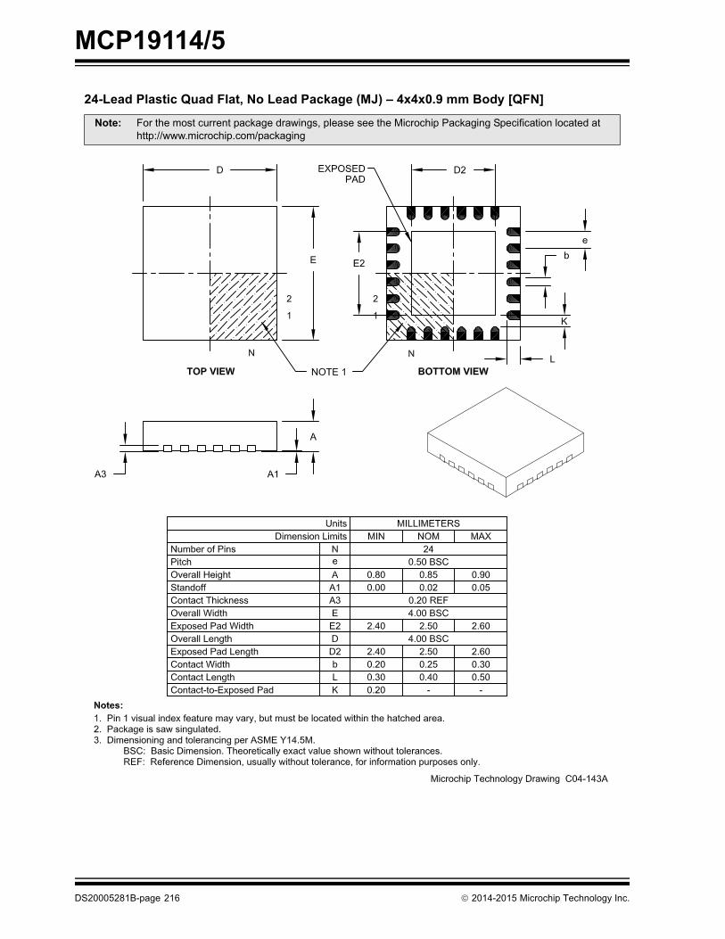
MCP19114/5
24-Lead Plastic Quad Flat, No Lead Package (MJ) – 4x4x0.9 mm Body [QFN]
Note: For the most current package drawings, please see the Microchip Packaging Specification located at http://www.microchip.com/packaging
DS20005281B-page 216 2014-2015 Microchip Technology Inc.

MCP19114/5
Note: For the most current package drawings, please see the Microchip Packaging Specification located at http://www.microchip.com/packaging
2014-2015 Microchip Technology Inc. DS20005281B-page 217
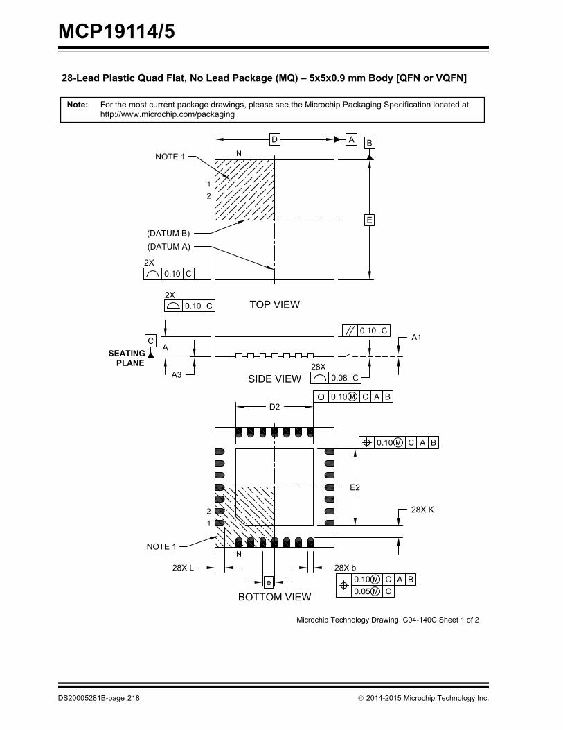
MCP19114/5
BA
0.10 C
0.10 C
0.10 C A B0.05 C
(DATUM B)(DATUM A)
NOTE 1
2XTOP VIEW
SIDE VIEW
BOTTOM VIEW
For the most current package drawings, please see the Microchip Packaging Specification located athttp://www.microchip.com/packaging
Note:
NOTE 1
12
N
0.10 C A B
0.10 C A B
0.10 C
0.08 C
Microchip Technology Drawing C04-140C Sheet 1 of 2
28-Lead Plastic Quad Flat, No Lead Package (MQ) – 5x5x0.9 mm Body [QFN or VQFN]
2X
28X
D
E
12
N
e
28X L
28X K
E2
D2
28X b
A3
AC
SEATINGPLANE
A1
DS20005281B-page 218 2014-2015 Microchip Technology Inc.
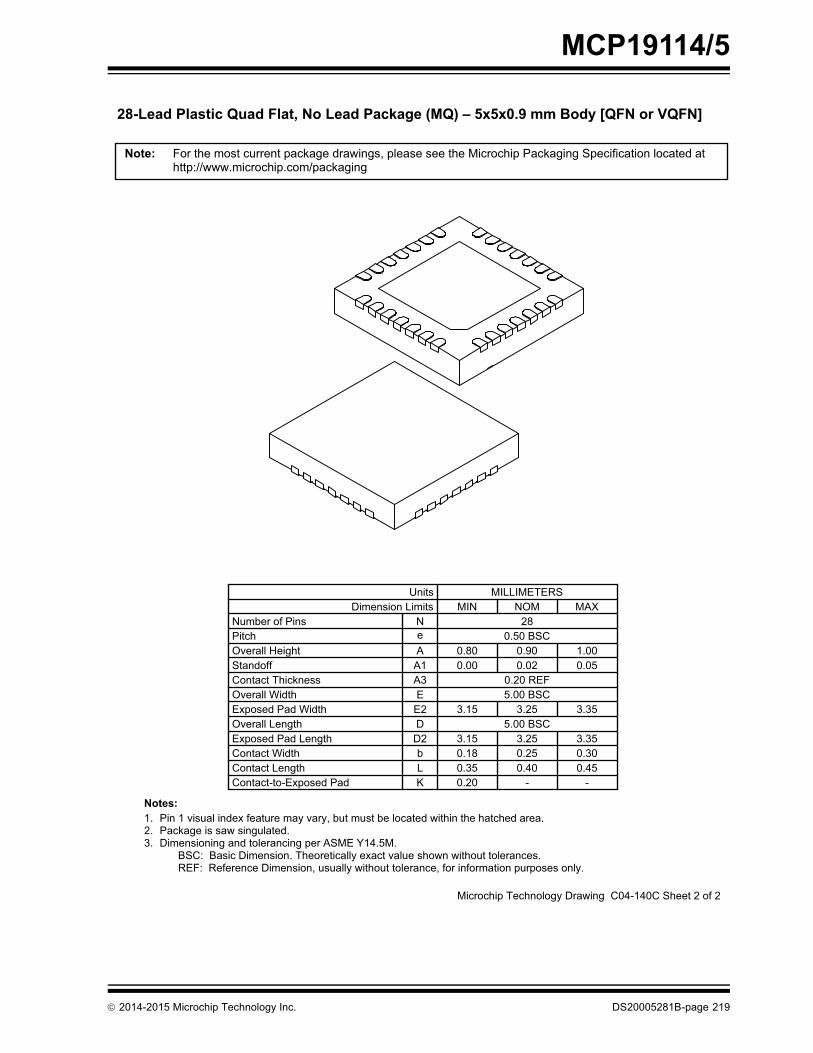
MCP19114/5
Microchip Technology Drawing C04-140C Sheet 2 of 2
For the most current package drawings, please see the Microchip Packaging Specification located athttp://www.microchip.com/packaging
Note:
28-Lead Plastic Quad Flat, No Lead Package (MQ) – 5x5x0.9 mm Body [QFN or VQFN]
Dimension LimitsUnits
D
Overall Width
Overall LengthExposed Pad Length
Exposed Pad Width
Contact Thickness
D2
E2E
3.35
MILLIMETERS
0.20 REF
MIN
A3
MAX
5.00 BSC3.25
Contact LengthContact Width
Lb
0.450.30
Notes:1.
KContact-to-Exposed Pad 0.20
NOM
BSC: Basic Dimension. Theoretically exact value shown without tolerances.3.2.
REF: Reference Dimension, usually without tolerance, for information purposes only.
Standoff A1 0.02Overall Height A 0.90Pitch e 0.50 BSCNumber of Pins N 28
0.350.183.15
3.15
0.000.80
0.250.40
-
3.255.00 BSC
3.35
0.051.00
-
Pin 1 visual index feature may vary, but must be located within the hatched area.
Dimensioning and tolerancing per ASME Y14.5M.Package is saw singulated.
2014-2015 Microchip Technology Inc. DS20005281B-page 219

MCP19114/5
28-Lead Plastic Quad Flat, No Lead Package (MQ) – 5x5 mm Body [QFN] Land PatternWith 0.55 mm Contact Length
Note: For the most current package drawings, please see the Microchip Packaging Specification located at http://www.microchip.com/packaging
Microchip Technology Drawing C04-2140A
DS20005281B-page 220 2014-2015 Microchip Technology Inc.
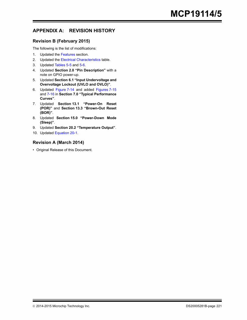
MCP19114/5
APPENDIX A: REVISION HISTORY
Revision B (February 2015)The following is the list of modifications:
1. Updated the Features section.2. Updated the Electrical Characteristics table.3. Updated Tables 5-5 and 5-6.4. Updated Section 2.0 “Pin Description” with a
note on GPIO power-up.5. Updated Section 6.1 “Input Undervoltage and
Overvoltage Lockout (UVLO and OVLO)”.6. Updated Figure 7-14 and added Figures 7-15
and 7-16 in Section 7.0 “Typical PerformanceCurves”.
7. Updated Section 13.1 “Power-On Reset(POR)” and Section 13.3 “Brown-Out Reset(BOR)”.
8. Updated Section 15.0 “Power-Down Mode(Sleep)”.
9. Updated Section 20.2 “Temperature Output”.10. Updated Equation 20-1.
Revision A (March 2014)• Original Release of this Document.
2014-2015 Microchip Technology Inc.
DS20005281B-page 221
MCP19114/5
NOTES:DS20005281B-page 222
2014-2015 Microchip Technology Inc.
MCP19114/5
INDEX
AA/DSpecifications...................................................... 3, 5, 35A/D Conversion. See ADCABECON Register .............................................................. 49Absolute Maximum Ratings ................................................ 22AC Characteristics .............................................................. 30ACKSTAT
Status Flag................................................................ 179ADC .................................................................................. 127
10-Bit Result Format ................................................. 129Acquisition Requirements ......................................... 133Associated Registers ................................................ 135Block Diagram........................................................... 127Calculating Acquisition Time..................................... 133Channel Selection..................................................... 128Configuration............................................................. 128Configuring Interrupt ................................................. 130Conversion Clock...................................................... 128Conversion Procedure .............................................. 130Internal Sampling Switch (RSS) Impedance.............. 133Interrupts................................................................... 129Operation .................................................................. 130Operation During Sleep ............................................ 130Port Configuration ..................................................... 128Register Definitions................................................... 131Requirements.............................................................. 35Source Impedance (RS)............................................ 133Timing Diagram........................................................... 36
ADCON0 Register....................................................... 57, 131ADCON1 Register............................................................. 132ADRESH Register............................................................. 132ADRESL Register ............................................................. 132Analog Blocks Enable Control ............................................ 49
Error Amplifier Disable ................................................ 49Analog Peripheral Control ................................................... 48
PWM Steering............................................................. 48Secondary Current Positive Sense Pull-Up ................ 48
Analog-to-Digital Converter. See ADCANSELA Register ............................................................. 114ANSELB Register ............................................................. 119Application Diagrams
MCP19114 Boost Quasi-Resonant............................. 11MCP19114 Cuk’ Synchronous Positive Output .......... 11
AssemblerMPASM Assembler................................................... 212
BBench Testing
System ........................................................................ 57BF ..................................................................................... 181
Status Flag................................................................ 179BF Status Flag .................................................................. 181Block Diagrams
ADC .......................................................................... 127ADC Transfer Function ............................................. 134Analog Input Model ................................................... 134Baud Rate Generator................................................ 190Capture Mode Operation .......................................... 149Compare Mode Operation ........................................ 150Interrupt Logic ............................................................. 94MCP19114/5 Flyback Synchronous Quasi-Resonant. 10Microcontroller Core.................................................... 12
2014-2015 Microchip Technology Inc.
MSSP (I2C Master Mode)......................................... 155MSSP (I2C Slave Mode)........................................... 156On-Chip Reset Circuit................................................. 85Pulse-Width Modulation (PWM) ............................... 146Recommended MCLR Circuit..................................... 86Timer0 ...................................................................... 137Timer1 ...................................................................... 139Timer2 ...................................................................... 143Watchdog Timer with Shared Prescale .................... 103
Brown-Out Reset (BOR) ..................................................... 87
CC Compilers
MPLAB XC ............................................................... 212Calibration Word Registers
CALWD1 (Calibration Word 1) ................................... 59CALWD10 (Calibration Word 10) ............................... 66CALWD11 (Calibration Word 11) ............................... 67CALWD2 (Calibration Word 2) ................................... 60CALWD3 (Calibration Word 3) ................................... 61CALWD4 (Calibration Word 4) ................................... 61CALWD5 (Calibration Word 5) ................................... 62CALWD6 (Calibration Word 6) ................................... 62CALWD7 (Calibration Word 7) ................................... 63CALWD8 (Calibration Word 8) ................................... 64CALWD9 (Calibration Word 9) ................................... 65
Capture ModeBlock Diagram .......................................................... 149
Capture/Compare (CCD) ModuleCapture Mode........................................................... 149
CCP1IF............................................................. 149CCX Pin Configuration ..................................... 149Prescaler .......................................................... 149Software Interrupt ............................................. 149Timer1 Mode Selection..................................... 149
Compare ModeCCP1IF............................................................. 150CMPX Pin Configuration................................... 150Software Interrupt ............................................. 150Special Event Trigger ....................................... 150Timer1 Mode Selection..................................... 150
Register .................................................................... 151CCDCON Register............................................................ 151Clock Switching .................................................................. 84Code Example
Indirect Addressing..................................................... 80Code Examples
A/D Conversion ........................................................ 130Assigning Prescaler to Timer0.................................. 138Assigning Prescaler to WDT..................................... 138Initializing PORTGPA ............................................... 111Saving Status and W Registers in RAM ................... 100
Compare ModeBlock Diagram .......................................................... 150
Computed Function Calls ................................................... 79Computed GOTO................................................................ 79Configuration Word............................................................. 81
Registers Associated with Clock Sources .................. 84with Watchdog Timer................................................ 104
Current Sense .................................................................... 19Customer Change Notification Service............................. 229Customer Support............................................................. 229
DS20005281B-page 223

MCP19114/5
DData MemoryCore Registers ............................................................ 71STATUS Register ............................................... 71
General Purpose Registers......................................... 70Map ............................................................................. 73Organization................................................................ 70Special Function Registers ................................... 70, 72
DC and AC Characteristics ................................................. 53Graphs and Tables ..................................................... 53
DEADCON Register............................................................ 45DESATCON Register.......................................................... 41Desaturation Detection for Quasi-Resonant Operation....... 41Development Support ....................................................... 211Device Calibration ............................................................... 59
CALWD1 (Calibration Word 1) .................................... 59CALWD10 (Calibration Word 10) ................................ 66CALWD11 (Calibration Word 11) ................................ 67CALWD2 (Calibration Word 2) .................................... 60CALWD3 (Calibration Word 3) .................................... 61CALWD4 (Calibration Word 4) .................................... 61CALWD5 (Calibration Word 5) .................................... 62CALWD6 (Calibration Word 6) .................................... 62CALWD7 (Calibration Word 7) .................................... 63CALWD8 (Calibration Word 8) .................................... 64CALWD9 (Calibration Word 9) .................................... 65
Device Configuration..................................................... 37, 81Code Protection .......................................................... 82Configuration Word ..................................................... 81ID Locations ................................................................ 82Write Protection .......................................................... 82
Device Overview ................................................................... 9Digital Electrical Characteristics.......................................... 29Direct Addressing................................................................ 80Driver Control Circuitry........................................................ 20
EElectrical Characteristics..................................................... 22Errata .................................................................................... 7External Clock
Timing ......................................................................... 30Timing Requirements.................................................. 30
FFeatures ................................................................................ 1
Microcontroller .............................................................. 1Timer0 Module .......................................................... 137Timer1 Module .......................................................... 139
File Select Register. See FSRFirmware Instructions........................................................ 199Flash Program Memory
Control ...................................................................... 105Operation During Code Protect......................... 109Operation During Write Protect......................... 109Protection Against Spurious Write .................... 109Registers........................................................... 106
Reading..................................................................... 108Writing to ................................................................... 109
FSRRegister....................................................................... 79
GGeneral Purpose Register. See GPRGPR
Register....................................................................... 70
DS20005281B-page 224
II/O
Ports ......................................................................... 111I2C Mode (MSSP)
Acknowledge Sequence ........................................... 160Acknowledge Sequence Timing ............................... 183Associated Registers ................................................ 189Bus Collision
During a Repeated Start Condition................... 187During a Start Condition ................................... 185During a Stop Condition ................................... 188
Effects of a Reset ..................................................... 184I2C Clock Rate w/BRG.............................................. 190Master Mode............................................................. 176
Clock Arbitration ............................................... 176Operation.......................................................... 176Reception ......................................................... 181Repeated Start Condition Timing ..................... 178Start Condition Timing ...................................... 177Transmission .................................................... 179
Multi-Master Communication, Bus Collision and Arbitra-tion.................................................................... 184
Multi-Master Mode .................................................... 184Operation .................................................................. 158Overview................................................................... 156Read/Write Bit Information (R/W Bit) ........................ 160Slave Mode
10-bit Address Reception ................................. 170Bus Collision..................................................... 166Clock Stretching ............................................... 174Clock Synchronization ...................................... 174General Call Address Support .......................... 175Operation.......................................................... 160SSPMSK1 Register .......................................... 175Transmission .................................................... 166
Sleep Operation........................................................ 184Stop Condition Timing .............................................. 183
ICLEBCON Register ........................................................... 43ICOACON Register............................................................. 42In-Circuit Serial Programming (ICSP)............................... 209
Common Programming Interfaces............................ 209INDF
Register ...................................................................... 79Indirect Addressing ....................................................... 79, 80Input.................................................................................... 22
Overvoltage Lockout................................................... 37Type............................................................................ 13Undervoltage Lockout................................................. 37
Instruction Format............................................................. 199Instruction Set................................................................... 199
ADDLW..................................................................... 201ADDWF..................................................................... 201ANDLW..................................................................... 201ANDWF..................................................................... 201BCF .......................................................................... 201BSF........................................................................... 201BTFSC...................................................................... 201BTFSS ...................................................................... 202CALL......................................................................... 202CLRF ........................................................................ 202CLRW ....................................................................... 202CLRWDT .................................................................. 202COMF ....................................................................... 202DECF........................................................................ 202DECFSZ ................................................................... 203
2014-2015 Microchip Technology Inc.

MCP19114/5
GOTO ....................................................................... 203INCF.......................................................................... 203INCFSZ..................................................................... 203IORLW ...................................................................... 203IORWF ...................................................................... 203MOVF........................................................................ 204MOVLW .................................................................... 204MOVWF .................................................................... 204NOP .......................................................................... 204RETFIE ..................................................................... 205RETLW ..................................................................... 205RETURN ................................................................... 205RLF ........................................................................... 205RRF........................................................................... 206SLEEP ...................................................................... 206SUBLW ..................................................................... 206SUBWF..................................................................... 206Summary Table......................................................... 200SWAPF ..................................................................... 206XORLW..................................................................... 206XORWF..................................................................... 207INTCON Register ................................................................ 95Internal Sampling Switch (RSS) Impedance...................... 133Internet Address................................................................ 229Interrupt-on-Change.......................................................... 121
Associated Registers ................................................ 123Clearing Interrupt Flags ............................................ 121Enabling the Module ................................................. 121Individual Pin Configuration ...................................... 121Operation in Sleep .................................................... 121Registers................................................................... 122
InterruptsADC .......................................................................... 130Associated Registers ................................................ 100Configuration Word w/ Clock Sources ........................ 84Context Saving.......................................................... 100Control Registers ........................................................ 95GPA2/INT.................................................................... 93Timer0....................................................................... 138Timer1....................................................................... 140
IOCA Register ................................................................... 122IOCB Register ................................................................... 122
LLeading Edge Blanking ....................................................... 43Linear Regulators................................................................ 19
MMagnetic Desaturation Detection ........................................ 19Master Synchronous Serial Port. See MSSPMCLR.................................................................................. 86
Internal ........................................................................ 86Memory Organization.......................................................... 69
Data ............................................................................ 70Program ...................................................................... 69
Microchip Internet Web Site .............................................. 229Mode and RFB MUX Control .............................................. 51MODECON Register ........................................................... 51MOSFET ............................................................................. 17
DriverDead Time .......................................................... 48Programmable Dead Time.................................. 45Undervoltage Lockout Selection ......................... 49
Gate Driver Enables.................................................... 48MPLAB Assembler, Linker, Librarian ................................ 212MPLAB ICD 3 In-Circuit Debugger System ...................... 213
2014-2015 Microchip Technology Inc.
MPLAB Integrated Development Environment Software.. 211MPLAB PM3 Device Programmer .................................... 213MPLAB REAL ICE In-Circuit Emulator System ................ 213MPLAB X SIM Software Simulator ................................... 213MPLINK Object Linker/MPLIB Object Librarian ................ 212MSSP ............................................................................... 155
Arbitration ................................................................. 157Baud Rate Generator ............................................... 190Block Diagram (I2C Master Mode)............................ 155Block Diagram (I2C Slave Mode).............................. 156Clock Stretching ....................................................... 157I2C Bus Terms .......................................................... 158I2C Master Mode ...................................................... 176I2C Mode .................................................................. 156I2C Mode Operation.................................................. 158I2C Slave Mode Operation........................................ 160Overview................................................................... 155
OOPCODE Field Descriptions............................................. 199OPTION_REG Register...................................................... 78Oscillator............................................................................. 83
Associated Registers.................................................. 84Calibration .................................................................. 83Delay Upon Base Frequency Change ........................ 84Delay Upon Power-Up................................................ 84Delay Upon Wake-Up................................................. 84Frequency Tuning....................................................... 83Internal........................................................................ 83
OSCTUNE Register............................................................ 83Output
Drive Circuitry ............................................................. 19Overvoltage ................................................................ 39
OVCON Register ................................................ 39OVREFCON Register......................................... 39Protection ........................................................... 39
Type............................................................................ 13Output Regulation Reference Voltage Configuration.......... 46OVCON Register ................................................................ 39Overvoltage Lockout
Input............................................................................ 37OVREFCON Register ......................................................... 39
PPackaging......................................................................... 215
Marking..................................................................... 215Specifications ........................................................... 216
PCL..................................................................................... 79Modifying .................................................................... 79
PCLATH ............................................................................. 79PCON Register ............................................................. 88, 91PE1 Register ...................................................................... 48Peak Current Mode............................................................. 19PICkit 3 In-Circuit Debugger/PICkit 3 In-Circuit Programmer .
213PIE1 Register ..................................................................... 96PIE2 Register ..................................................................... 97Pin Diagram
24-Pin QFN (MCP19114) ............................................. 228-Pin QFN (MCP19115) ............................................. 4
Pinout DescriptionSummary .................................................................. 3, 5Table........................................................................... 13
PIR1 Register ..................................................................... 98PIR2 Register ..................................................................... 99PMADRH Register.................................................... 105, 107
DS20005281B-page 225

MCP19114/5
PMADRL Register..................................................... 105, 106PMCON1 Register .................................................... 105, 107PMCON2 Register ............................................................ 105PMDATH Register............................................................. 106PMDATL Register ............................................................. 106PORTGPA................................................................. 111, 121ANSELA Register ..................................................... 112Associated Registers ................................................ 115Functions and Output Priorities................................. 112Interrupt-on-Change.................................................. 111Output Priority ........................................................... 112Register............................................................. 111, 113Weak Pull-Ups .......................................................... 111
PORTGPB................................................................. 116, 121ANSELB Register ..................................................... 116Associated Registers ................................................ 119Functions and Output Priorities................................. 117Interrupt-on-Change.................................................. 116Output Priority ........................................................... 117Register............................................................. 116, 117Weak Pull-Ups .......................................................... 116
Power-Down Mode (Sleep) ............................................... 101Associated Registers ................................................ 102
Power-On Reset (POR) ...................................................... 86Power-Up Timer (PWRT) .................................................... 88Primary Input Current Offset Adjust .................................... 42Program Memory
Map and Stack (MCP19114)....................................... 69Organization................................................................ 69Protection.................................................................... 82
Programming, Device Instructions .................................... 199Pulse-Width Modulation
Control Logic............................................................. 153Pulse-Width Modulation. See PWMPWM ................................................................................... 34
Associated Registers ................................................ 147Control Logic............................................................. 153Duty Cycle................................................................. 147Enhanced Module ..................................................... 145Fixed Frequency ......................................................... 20Operation During Sleep ............................................ 147Output ....................................................................... 146Period........................................................................ 146Requirements.............................................................. 34Simplified Diagram.................................................... 146Stand-alone Mode..................................................... 145Standard Mode ......................................................... 145Steering....................................................................... 48Switching Frequency Synchronization Mode ............ 145Timing Diagram........................................................... 34
RRead-Modify-Write Operations.......................................... 199Registers
ABECON (Analog Block Enable Control).................... 49ADCON0 (A/D Control 0) .......................................... 131ADCON0 (Analog-to-Digital Control) .......................... 57ADCON1 (A/D Control 1) .......................................... 132ADRESH (ADC Result High) .................................... 132ADRESL (ADC Result Low)...................................... 132ANSELA (Analog Select GPA).................................. 114ANSELB (Analog Select GPB).................................. 119CALWD1 (Calibration Word 1) .................................... 59CALWD10 (Calibration Word 10) ................................ 66CALWD11 (Calibration Word 11) ................................ 67CALWD2 (Calibration Word 2) .................................... 60
DS20005281B-page 226
CALWD3 (Calibration Word 3).................................... 61CALWD4 (Calibration Word 4).................................... 61CALWD5 (Calibration Word 5).................................... 62CALWD6 (Calibration Word 6).................................... 62CALWD7 (Calibration Word 7).................................... 63CALWD8 (Calibration Word 8).................................... 64CALWD9 (Calibration Word 9).................................... 65CCDCON (Dual Capture/Compare Control Module) 151CONFIG (Configuration Word) ................................... 81DEADCON (Driver Dead Time Control)...................... 45DESATCON (Desaturation Comparator Control) ....... 41FSR (File Select Register) .......................................... 79General Purpose Register .......................................... 70ICLEBCON (Input Current Leading Edge Blanking Con-
trol) ..................................................................... 43ICOACON (Input Current Offset Adjust Control) ........ 42INDF ........................................................................... 79INTCON (Interrupt Control)......................................... 95IOCA (Interrupt-on-Change PORTGPA)................... 122IOCB (Interrupt-on-Change PORTGPB)................... 122MODECON (Master/Slave and RFB MUX Control).... 51OPTION_REG (Option) .............................................. 78OSCTUNE (Oscillator Tuning).................................... 83OVCON (Output Overvoltage Comparator Control) ... 39OVREFCON (Output Overvoltage Detect Level)........ 39PCON (Power Control) ......................................... 88, 91PE1 (Analog Peripheral Enable1 Control) .................. 48PIE1 (Peripheral Interrupt Enable 1)........................... 96PIE2 (Peripheral Interrupt Enable 2)........................... 97PIR1 (Peripheral Interrupt Flag 1)............................... 98PIR2 (Peripheral Interrupt Flag 2)............................... 99PMADRH (Program Memory Address High) .... 105, 107PMADRL (Program Memory Address Low)...... 105, 106PMCON1 (Program Memory Control 1)............ 105, 107PMCON2 (Program Memory Control 2).................... 105PMDATH (Program Memory Data High) .................. 106PMDATL (Program Memory Data Low).................... 106PORTGPA ........................................................ 111, 113PORTGPB ........................................................ 116, 117SLPCRCON (Slope Compensation Ramp Control).... 44Special Function ......................................................... 70Special Registers Summary
Bank 0 ................................................................ 74Bank 1 ................................................................ 75Bank 2 ................................................................ 76Bank 3 ................................................................ 77
SSPADD (MSSP Address and Baud Rate 1) ........... 196SSPADD2 (MSSP Address 2) .................................. 197SSPCON1 (SSP Control 1) ...................................... 192SSPCON2 (SSP Control 2) ...................................... 194SSPCON3 (SSP Control 3) ...................................... 195SSPMSK (SSP Mask 1)............................................ 196SSPMSK1 (SSP Mask)............................................. 175SSPMSK2 (SSP Mask 2).......................................... 197SSPSTAT (SSP Status)............................................ 191STATUS ..................................................................... 71T1CON (Timer1 Control) .......................................... 140T2CON (Timer2 Control) .......................................... 144TRISGPA (PORTGPA Tri-State) ...................... 111, 113TRISGPB (PORTGPB Tri-State) ...................... 116, 118VINCON (UVLO and OVLO Comparator Control) ...... 37VINOVLO (Input Overvoltage Lockout) ...................... 38VINUVLO (Input Undervoltage Lockout)..................... 38VREF2CON (VREF2 Voltage Set Point) ...................... 47VREFCON (Current/Voltage Regulation Set Point Con-
2014-2015 Microchip Technology Inc.
MCP19114/5
trol)...................................................................... 46WPUGPA (Weak Pull-Up PORTGPA) ...................... 114WPUGPB (Weak Pull-Up PORTGPB) ...................... 118
RequirementsA/D Acquisition.......................................................... 133A/D Conversion........................................................... 35External Clock, Timing ................................................ 30I/O, Timing .................................................................. 31PWM ........................................................................... 34Reset, Watchdog Timer, Oscillator Start-Up Timer and
Power-Up Timer.................................................. 33Timer0 External Clock................................................. 34
Resets................................................................................. 85Associated Registers .................................................. 91Brown-Out................................................................... 87Determining Causes ................................................... 89Power-On.................................................................... 86Watchdog Timer.......................................................... 88
SSleep
Wake-Up from........................................................... 101Wake-Up Using Interrupts......................................... 102
Slope Compensation........................................................... 44SLPCRCON Register.......................................................... 44Software Simulator (MPLAB X SIM) ................................. 213Special Event Trigger
Capture/Compare Module......................................... 150Special Function Registers (SFR)....................................... 70SSPADD Register ............................................................. 196SSPADD2 Register ........................................................... 197SSPCON1 Register .......................................................... 192SSPCON2 Register .......................................................... 194SSPCON3 Register .......................................................... 195SSPMSK Register............................................................. 196SSPMSK1 Register........................................................... 175SSPMSK2 Register........................................................... 197SSPOV.............................................................................. 181SSPOV Status Flag .......................................................... 181SSPSTAT Register ........................................................... 191
R/W Bit...................................................................... 160Stack ................................................................................... 79Start-Up............................................................................... 20Start-Up Sequence ............................................................. 88STATUS Register ............................................................... 71System Bench Testing ........................................................ 57
TT1CON Register ............................................................... 140T2CON Register ............................................................... 144Temperature Indicator Module.......................................... 125
Circuit Operation ....................................................... 125Temperature Output.................................................. 125
Thermal Specifications........................................................ 28Timer0............................................................................... 137
8-bit Counter Mode ................................................... 1378-bit Timer Mode....................................................... 137Associated Registers ................................................ 138Block Diagram........................................................... 137External Clock........................................................... 138
Requirements ..................................................... 34Timing ................................................................. 33
Interrupt..................................................................... 138Module ...................................................................... 137
Features............................................................ 137Operation .................................................................. 137
2014-2015 Microchip Technology Inc.
During Sleep..................................................... 138Software Programmable Prescaler........................... 137Switching Prescaler .................................................. 138T0CKI ....................................................................... 138TMR0 Register ......................................................... 137
Timer1 .............................................................................. 139Associated Registers................................................ 141Block Diagram .......................................................... 139Clock Source Selection ............................................ 139Control Register........................................................ 140External Clock Timing................................................. 33Interrupt .................................................................... 140Module...................................................................... 139
Features ........................................................... 139Operation.................................................................. 139
During Sleep..................................................... 140Prescaler .................................................................. 140TMR1H Register....................................................... 139TMR1L Register ....................................................... 139
Timer2Associated Registers................................................ 144Block Diagram .......................................................... 143Control Register........................................................ 144Module...................................................................... 143
Features ........................................................... 143Operation.................................................................. 143
TimersTimer1 (T1CON)....................................................... 139Timer2 (T2CON)....................................................... 143
Timing DiagramsA/D Conversion .......................................................... 36Acknowledge Sequence ........................................... 183Baud Rate Generator with Clock Arbitration............. 177BRG Reset Due to SDA Arbitration During Start Condi-
tion.................................................................... 186Bus Collision During a Repeated Start Condition (Case
1) ...................................................................... 187Bus Collision During a Repeated Start Condition (Case
2) ...................................................................... 187Bus Collision During a Start Condition (SCL = 0) ..... 186Bus Collision During a Start Condition (SDA Only) .. 185Bus Collision During a Stop Condition (Case 1)....... 188Bus Collision During a Stop Condition (Case 2)....... 188Bus Collision for Transmit and Acknowledge ........... 184Clock Synchronization .............................................. 174First Start Bit ............................................................. 177I/O............................................................................... 31I2C Master Mode (7 or 10-Bit Transmission) ............ 180I2C Master Mode (7-Bit Reception) .......................... 182INT Pin Interrupt ......................................................... 94Power-Up Timer ......................................................... 32Pulse-Width Modulation.............................................. 34Repeat Start Condition ............................................. 178Reset .......................................................................... 32Start-Up Timer ............................................................ 32Stop Condition Receive or Transmit Mode............... 183Time-Out Sequence
Case 1 ................................................................ 88Case 2 ................................................................ 89Case 3 ................................................................ 89
Timer0, External Clock ............................................... 33Timer1, External Clock ............................................... 33Wake-up from Interrupt............................................. 102Watchdog Timer ......................................................... 32
Timing Parameter Symbology ............................................ 29
DS20005281B-page 227
MCP19114/5
TRISGPA .......................................................................... 111Register............................................................. 111, 113TRISGPB .......................................................................... 116
Register............................................................. 116, 118Typical Performance Curves............................................... 53
UUndervoltage Lockout
Input ............................................................................ 37Selection for MOSFET Driver ..................................... 49
VVINCON Register................................................................ 37VINOVLO Register.............................................................. 38VINUVLO Register .............................................................. 38VREF2 Voltage Reference.................................................... 47VREF2CON Register .......................................................... 47VREFCON Register ............................................................ 46
WWatchdog Timer. See WDTWCOL ............................................................................... 183
Status Flag........................................ 177, 179, 181, 183WCOL Status Flag ............................................................ 183WDT.................................................................................. 103
Associated Registers ................................................ 104Block Diagram........................................................... 103Configuration Word w/ Watchdog Timer ................... 104Operation .................................................................. 103Period........................................................................ 103Programming Considerations ................................... 103Reset........................................................................... 88Switching Prescaler .................................................. 138
WPUGPA Register............................................................ 114WPUGPB Register............................................................ 118WWW Address.................................................................. 229WWW, On-Line Support........................................................ 7
DS20005281B-page 228
2014-2015 Microchip Technology Inc.
MCP19114/5
THE MICROCHIP WEB SITEMicrochip provides online support via our web site atwww.microchip.com. This web site is used as a meansto make files and information easily available tocustomers. Accessible by using your favorite Internetbrowser, the web site contains the followinginformation:
• Product Support – Data sheets and errata, application notes and sample programs, design resources, user’s guides and hardware support documents, latest software releases and archived software
• General Technical Support – Frequently Asked Questions (FAQ), technical support requests, online discussion groups, Microchip consultant program member listing
• Business of Microchip – Product selector and ordering guides, latest Microchip press releases, listing of seminars and events, listings of Microchip sales offices, distributors and factory representatives
CUSTOMER CHANGE NOTIFICATION SERVICEMicrochip’s customer notification service helps keepcustomers current on Microchip products. Subscriberswill receive e-mail notification whenever there arechanges, updates, revisions or errata related to aspecified product family or development tool of interest.
To register, access the Microchip web site atwww.microchip.com. Under “Support”, click on“Customer Change Notification” and follow theregistration instructions.
2014-2015 Microchip Technology Inc.
CUSTOMER SUPPORTUsers of Microchip products can receive assistancethrough several channels:
• Distributor or Representative• Local Sales Office• Field Application Engineer (FAE)• Technical Support
Customers should contact their distributor,representative or Field Application Engineer (FAE) forsupport. Local sales offices are also available to helpcustomers. A listing of sales offices and locations isincluded in the back of this document.
Technical support is available through the web siteat: http://www.microchip.com/support
DS20005281B-page 229

MCP19114/5
NOTES:DS20005281B-page 230
2014-2015 Microchip Technology Inc.
MCP19114/5
PRODUCT IDENTIFICATION SYSTEMTo order or obtain information, e.g., on pricing or delivery, refer to the factory or the listed sales office.
PART NO. X /XX XXX
PatternPackageTemperatureRange
Device
Device: MCP19114: Digitally Enhanced PWM Power AnalogHigh-Speed Controller
MCP19115: Digitally Enhanced PWM Power AnalogHigh-Speed Controller
Tape and Reel Option:
Blank = Standard packaging (tube)T = Tape and Reel
Temperature Range:
E = -40C to +125C (Extended)
Package: MJ = 24-Lead Plastic Quad Flat, No Lead Package - 4x4x0.9 mm Body (QFN)
MQ = 28-Lead Plastic Quad Flat, No Lead Package - 5x5x0.9 mm Body (QFN)
Examples:
a) MCP19114-E/MJ: Extended Temperature,24 LD QFN 4x4 package
b) MCP19114T-E/MJ: Tape and Reel,Extended Temperature,24 LD QFN 4x4 package
a) MCP19115-E/MQ: Extended Temperature,28 LD QFN 5x5 package
b) MCP19115T-E/MQ: Tape and Reel,Extended Temperature,28 LD QFN 5x5 package
Note 1: Tape and Reel identifier only appears inthe catalog part number description. Thisidentifier is used for ordering purposesand is not printed on the device package.Check with your Microchip Sales Officefor package availability with the Tape andReel option.
[X](1)
Tape and ReelOption
-
2014-2015 Microchip Technology Inc.
DS20005281B-page 231
MCP19114/5
NOTES:DS20005281B-page 232
2014-2015 Microchip Technology Inc.
Information contained in this publication regarding deviceapplications and the like is provided only for your convenienceand may be superseded by updates. It is your responsibility toensure that your application meets with your specifications.MICROCHIP MAKES NO REPRESENTATIONS ORWARRANTIES OF ANY KIND WHETHER EXPRESS ORIMPLIED, WRITTEN OR ORAL, STATUTORY OROTHERWISE, RELATED TO THE INFORMATION,INCLUDING BUT NOT LIMITED TO ITS CONDITION,QUALITY, PERFORMANCE, MERCHANTABILITY ORFITNESS FOR PURPOSE. Microchip disclaims all liabilityarising from this information and its use. Use of Microchipdevices in life support and/or safety applications is entirely atthe buyer’s risk, and the buyer agrees to defend, indemnify andhold harmless Microchip from any and all damages, claims,suits, or expenses resulting from such use. No licenses areconveyed, implicitly or otherwise, under any Microchipintellectual property rights.
2014-2015 Microchip Technology Inc.
QUALITY MANAGEMENT SYSTEM CERTIFIED BY DNV
== ISO/TS 16949 ==
Trademarks
The Microchip name and logo, the Microchip logo, dsPIC, FlashFlex, flexPWR, JukeBlox, KEELOQ, KEELOQ logo, Kleer, LANCheck, MediaLB, MOST, MOST logo, MPLAB, OptoLyzer, PIC, PICSTART, PIC32 logo, RightTouch, SpyNIC, SST, SST Logo, SuperFlash and UNI/O are registered trademarks of Microchip Technology Incorporated in the U.S.A. and other countries.
The Embedded Control Solutions Company and mTouch are registered trademarks of Microchip Technology Incorporated in the U.S.A.
Analog-for-the-Digital Age, BodyCom, chipKIT, chipKIT logo, CodeGuard, dsPICDEM, dsPICDEM.net, ECAN, In-Circuit Serial Programming, ICSP, Inter-Chip Connectivity, KleerNet, KleerNet logo, MiWi, MPASM, MPF, MPLAB Certified logo, MPLIB, MPLINK, MultiTRAK, NetDetach, Omniscient Code Generation, PICDEM, PICDEM.net, PICkit, PICtail, RightTouch logo, REAL ICE, SQI, Serial Quad I/O, Total Endurance, TSHARC, USBCheck, VariSense, ViewSpan, WiperLock, Wireless DNA, and ZENA are trademarks of Microchip Technology Incorporated in the U.S.A. and other countries.
SQTP is a service mark of Microchip Technology Incorporated in the U.S.A.
Silicon Storage Technology is a registered trademark of Microchip Technology Inc. in other countries.
GestIC is a registered trademarks of Microchip Technology Germany II GmbH & Co. KG, a subsidiary of Microchip Technology Inc., in other countries.
All other trademarks mentioned herein are property of their respective companies.
© 2014-2015, Microchip Technology Incorporated, Printed in the U.S.A., All Rights Reserved.
ISBN: 978-1-63277-090-5
Microchip received ISO/TS-16949:2009 certification for its worldwide
Note the following details of the code protection feature on Microchip devices:• Microchip products meet the specification contained in their particular Microchip Data Sheet.
• Microchip believes that its family of products is one of the most secure families of its kind on the market today, when used in the intended manner and under normal conditions.
• There are dishonest and possibly illegal methods used to breach the code protection feature. All of these methods, to our knowledge, require using the Microchip products in a manner outside the operating specifications contained in Microchip’s Data Sheets. Most likely, the person doing so is engaged in theft of intellectual property.
• Microchip is willing to work with the customer who is concerned about the integrity of their code.
• Neither Microchip nor any other semiconductor manufacturer can guarantee the security of their code. Code protection does not mean that we are guaranteeing the product as “unbreakable.”
Code protection is constantly evolving. We at Microchip are committed to continuously improving the code protection features of ourproducts. Attempts to break Microchip’s code protection feature may be a violation of the Digital Millennium Copyright Act. If such actsallow unauthorized access to your software or other copyrighted work, you may have a right to sue for relief under that Act.
headquarters, design and wafer fabrication facilities in Chandler and Tempe, Arizona; Gresham, Oregon and design centers in California and India. The Company’s quality system processes and procedures are for its PIC® MCUs and dsPIC® DSCs, KEELOQ® code hopping devices, Serial EEPROMs, microperipherals, nonvolatile memory and analog products. In addition, Microchip’s quality system for the design and manufacture of development systems is ISO 9001:2000 certified.
DS20005281B-page 233

Worldwide Sales and Service
DS20005281B-page 234 2014-2015 Microchip Te
AMERICASCorporate Office2355 West Chandler Blvd.Chandler, AZ 85224-6199Tel: 480-792-7200 Fax: 480-792-7277Technical Support: http://www.microchip.com/supportWeb Address: www.microchip.comAtlantaDuluth, GA Tel: 678-957-9614 Fax: 678-957-1455Austin, TXTel: 512-257-3370 BostonWestborough, MA Tel: 774-760-0087 Fax: 774-760-0088ChicagoItasca, IL Tel: 630-285-0071 Fax: 630-285-0075ClevelandIndependence, OH Tel: 216-447-0464 Fax: 216-447-0643DallasAddison, TX Tel: 972-818-7423 Fax: 972-818-2924DetroitNovi, MI Tel: 248-848-4000Houston, TX Tel: 281-894-5983IndianapolisNoblesville, IN Tel: 317-773-8323Fax: 317-773-5453Los AngelesMission Viejo, CA Tel: 949-462-9523 Fax: 949-462-9608New York, NY Tel: 631-435-6000San Jose, CA Tel: 408-735-9110Canada - TorontoTel: 905-673-0699 Fax: 905-673-6509
ASIA/PACIFICAsia Pacific OfficeSuites 3707-14, 37th FloorTower 6, The GatewayHarbour City, KowloonHong KongTel: 852-2943-5100Fax: 852-2401-3431Australia - SydneyTel: 61-2-9868-6733Fax: 61-2-9868-6755China - BeijingTel: 86-10-8569-7000 Fax: 86-10-8528-2104China - ChengduTel: 86-28-8665-5511Fax: 86-28-8665-7889China - ChongqingTel: 86-23-8980-9588Fax: 86-23-8980-9500China - DongguanTel: 86-769-8702-9880 China - HangzhouTel: 86-571-8792-8115 Fax: 86-571-8792-8116China - Hong Kong SARTel: 852-2943-5100 Fax: 852-2401-3431China - NanjingTel: 86-25-8473-2460Fax: 86-25-8473-2470China - QingdaoTel: 86-532-8502-7355Fax: 86-532-8502-7205China - ShanghaiTel: 86-21-5407-5533 Fax: 86-21-5407-5066China - ShenyangTel: 86-24-2334-2829Fax: 86-24-2334-2393China - ShenzhenTel: 86-755-8864-2200 Fax: 86-755-8203-1760China - WuhanTel: 86-27-5980-5300Fax: 86-27-5980-5118China - XianTel: 86-29-8833-7252Fax: 86-29-8833-7256
ASIA/PACIFICChina - XiamenTel: 86-592-2388138 Fax: 86-592-2388130China - ZhuhaiTel: 86-756-3210040 Fax: 86-756-3210049India - BangaloreTel: 91-80-3090-4444 Fax: 91-80-3090-4123India - New DelhiTel: 91-11-4160-8631Fax: 91-11-4160-8632India - PuneTel: 91-20-3019-1500Japan - OsakaTel: 81-6-6152-7160 Fax: 81-6-6152-9310Japan - TokyoTel: 81-3-6880- 3770 Fax: 81-3-6880-3771Korea - DaeguTel: 82-53-744-4301Fax: 82-53-744-4302Korea - SeoulTel: 82-2-554-7200Fax: 82-2-558-5932 or 82-2-558-5934Malaysia - Kuala LumpurTel: 60-3-6201-9857Fax: 60-3-6201-9859Malaysia - PenangTel: 60-4-227-8870Fax: 60-4-227-4068Philippines - ManilaTel: 63-2-634-9065Fax: 63-2-634-9069SingaporeTel: 65-6334-8870Fax: 65-6334-8850Taiwan - Hsin ChuTel: 886-3-5778-366Fax: 886-3-5770-955Taiwan - KaohsiungTel: 886-7-213-7828Taiwan - TaipeiTel: 886-2-2508-8600 Fax: 886-2-2508-0102Thailand - BangkokTel: 66-2-694-1351Fax: 66-2-694-1350
EUROPEAustria - WelsTel: 43-7242-2244-39Fax: 43-7242-2244-393Denmark - CopenhagenTel: 45-4450-2828 Fax: 45-4485-2829France - ParisTel: 33-1-69-53-63-20 Fax: 33-1-69-30-90-79Germany - DusseldorfTel: 49-2129-3766400Germany - MunichTel: 49-89-627-144-0 Fax: 49-89-627-144-44Germany - PforzheimTel: 49-7231-424750Italy - Milan Tel: 39-0331-742611 Fax: 39-0331-466781Italy - VeniceTel: 39-049-7625286 Netherlands - DrunenTel: 31-416-690399 Fax: 31-416-690340Poland - WarsawTel: 48-22-3325737 Spain - MadridTel: 34-91-708-08-90Fax: 34-91-708-08-91Sweden - StockholmTel: 46-8-5090-4654UK - WokinghamTel: 44-118-921-5800Fax: 44-118-921-5820
01/27/15
chnology Inc.