using verilog in the xilinx ise - university of idaho verilog in the...logic design: verilog using...
TRANSCRIPT
Logic Design: Verilog using Xilinx, 7-Segment Display.1 S. Yoder ND, 2012
CSE 20221: Logic Design
Using Verilog in the Xilinx ISE

Logic Design: Verilog using Xilinx, 7-Segment Display.2 S. Yoder ND, 2012
Steps in using Xilinx with Verilog
1. Create a new project
2. Determine inputs and outputs
3. Add a new Verilog source and fill in Inputs/outputs
4. Enter the description of the circuit
5. Perform a syntax check
6. Switch the design view to simulation
7. Select the design file and add new Verilog test
fixture source
Logic Design: Verilog using Xilinx, 7-Segment Display.3 S. Yoder ND, 2012
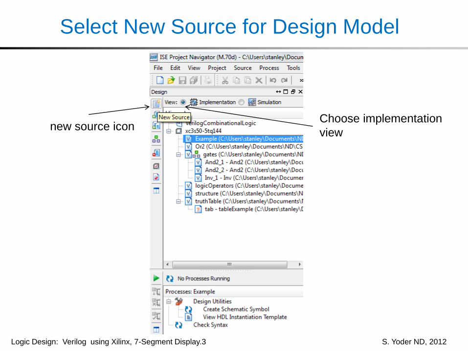
Select New Source for Design Model
new source icon Choose implementation
view
Logic Design: Verilog using Xilinx, 7-Segment Display.4 S. Yoder ND, 2012
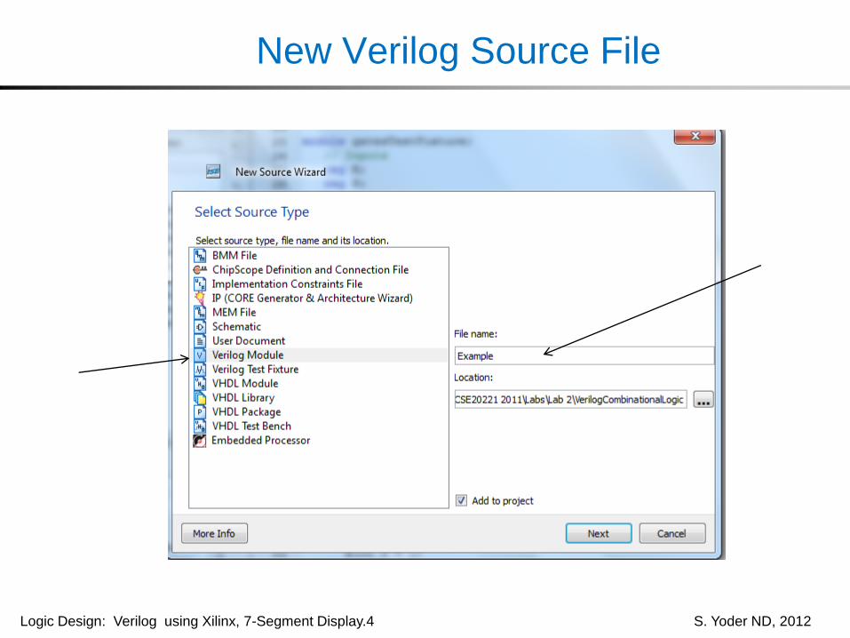
New Verilog Source File
Logic Design: Verilog using Xilinx, 7-Segment Display.5 S. Yoder ND, 2012
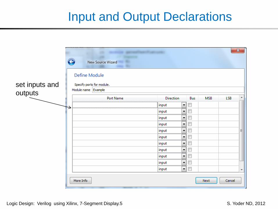
Input and Output Declarations
set inputs and
outputs

Logic Design: Verilog using Xilinx, 7-Segment Display.6 S. Yoder ND, 2012
Enter Design Model (structure example)
Logic Design: Verilog using Xilinx, 7-Segment Display.7 S. Yoder ND, 2012
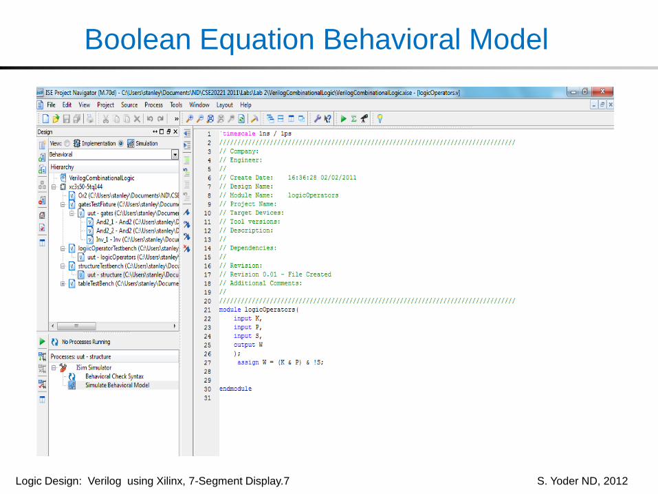
Boolean Equation Behavioral Model

Logic Design: Verilog using Xilinx, 7-Segment Display.8 S. Yoder ND, 2012
Select New Source for Test Fixture
File associated with
test fixture
new source icon
Choose simulation view
Logic Design: Verilog using Xilinx, 7-Segment Display.9 S. Yoder ND, 2012
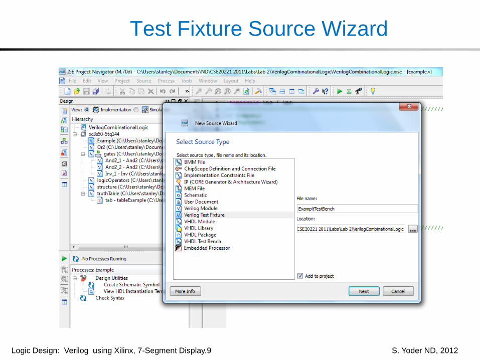
Test Fixture Source Wizard
Logic Design: Verilog using Xilinx, 7-Segment Display.10 S. Yoder ND, 2012
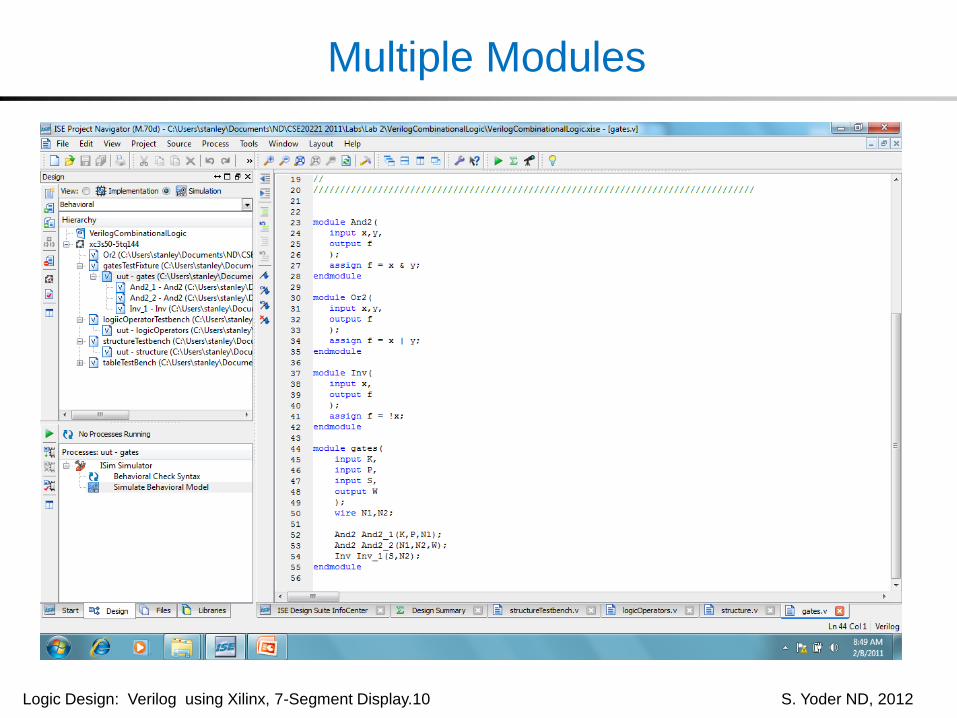
Multiple Modules

Logic Design: Verilog using Xilinx, 7-Segment Display.11 S. Yoder ND, 2012
Verilog Test Fixture
Note hierarchy
Logic Design: Verilog using Xilinx, 7-Segment Display.12 S. Yoder ND, 2012
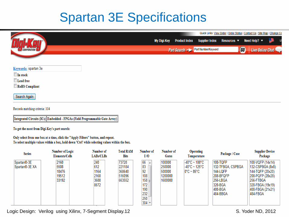
Spartan 3E Specifications
Logic Design: Verilog using Xilinx, 7-Segment Display.13 S. Yoder ND, 2012
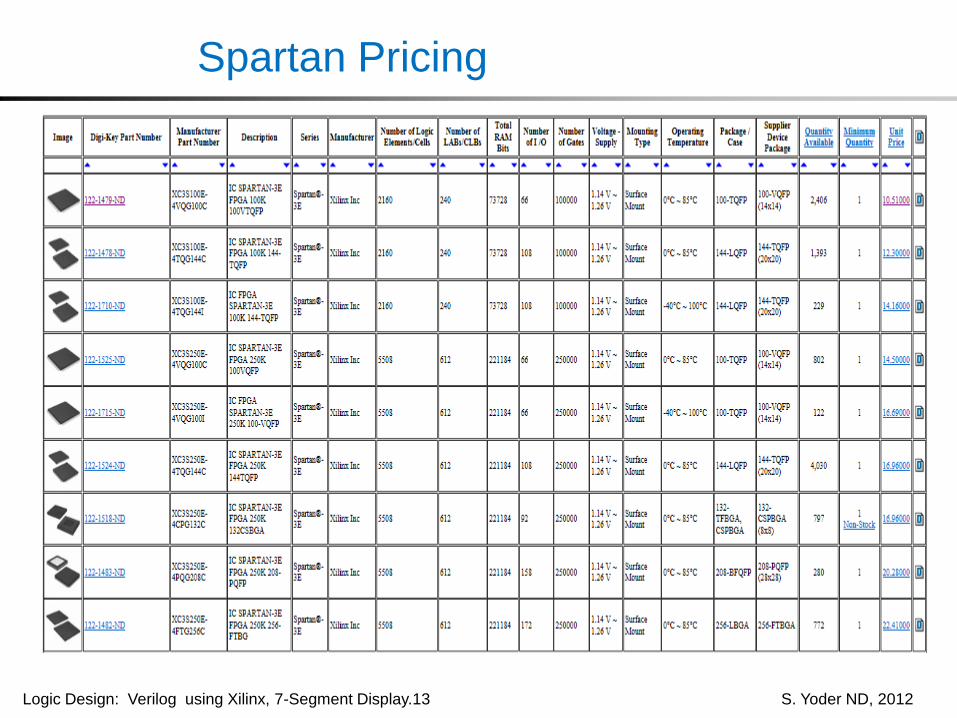
Spartan Pricing

Logic Design: Verilog using Xilinx, 7-Segment Display.14 S. Yoder ND, 2012
CSE 20221: Logic Design
Using the 4-Digit 7-Segment Display on
the Digilent Basys Board
https://www.digilentinc.com/Data/Products/BASYS2/Basys2_rm.pdf
listed under links in course web site

Logic Design: Verilog using Xilinx, 7-Segment Display.15 S. Yoder ND, 2012
LEDs
anode (+) cathode (-)
Digilent Basys board
Spartan 3E pin out
current limiting resistor
current flow
Logic Design: Verilog using Xilinx, 7-Segment Display.16 S. Yoder ND, 2012
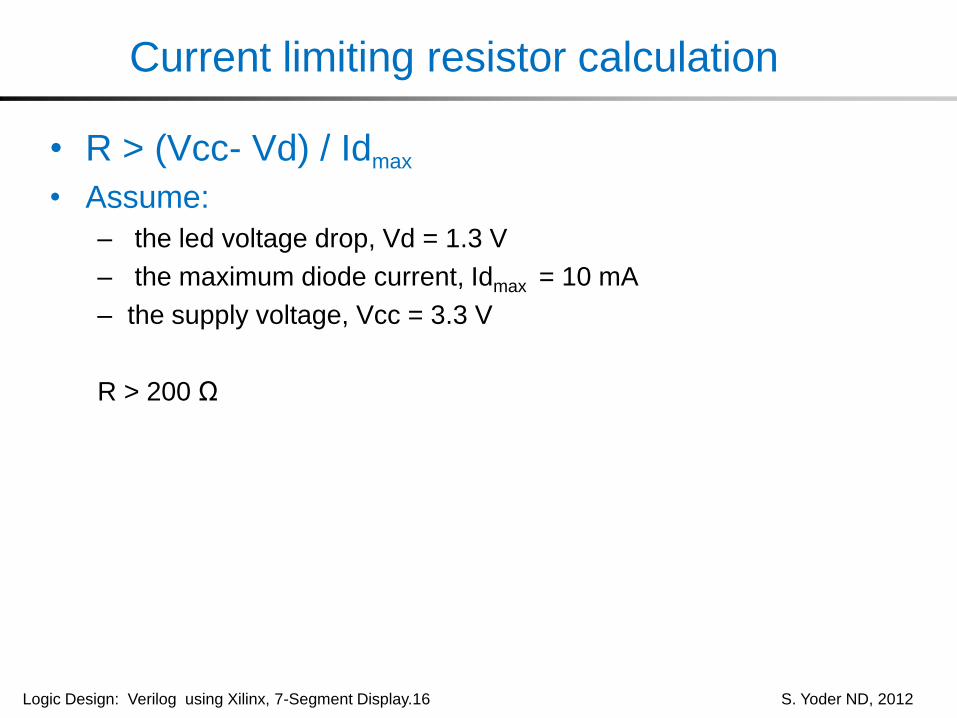
Current limiting resistor calculation
• R > (Vcc- Vd) / Idmax
• Assume:
– the led voltage drop, Vd = 1.3 V
– the maximum diode current, Idmax = 10 mA
– the supply voltage, Vcc = 3.3 V
R > 200 Ω
Logic Design: Verilog using Xilinx, 7-Segment Display.17 S. Yoder ND, 2012
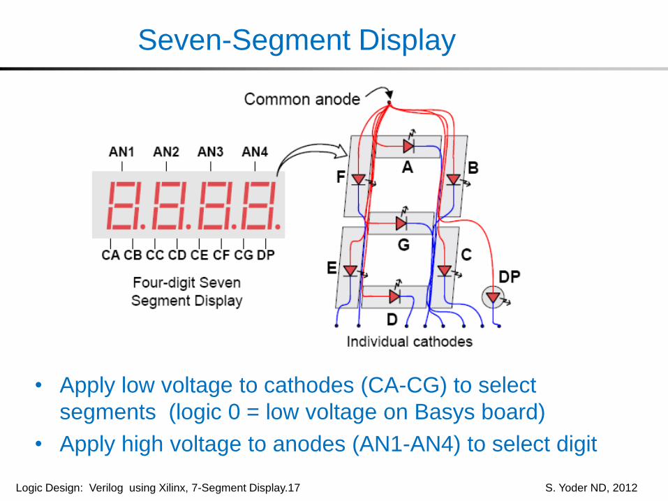
Seven-Segment Display
• Apply low voltage to cathodes (CA-CG) to select
segments (logic 0 = low voltage on Basys board)
• Apply high voltage to anodes (AN1-AN4) to select digit
Logic Design: Verilog using Xilinx, 7-Segment Display.18 S. Yoder ND, 2012
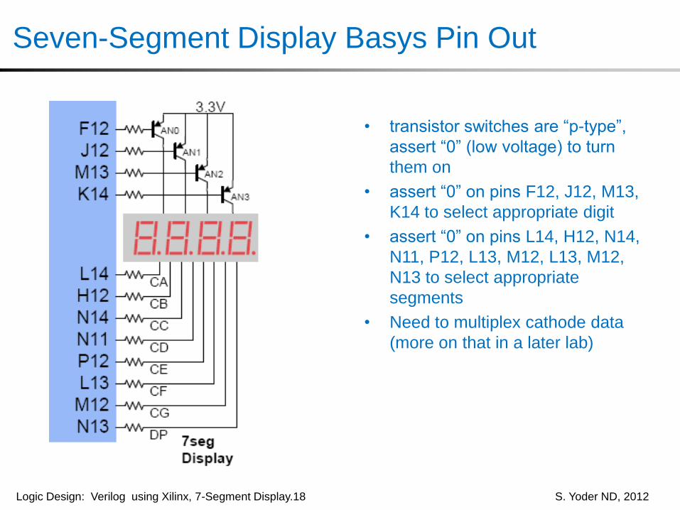
Seven-Segment Display Basys Pin Out
• transistor switches are “p-type”,
assert “0” (low voltage) to turn
them on
• assert “0” on pins F12, J12, M13,
K14 to select appropriate digit
• assert “0” on pins L14, H12, N14,
N11, P12, L13, M12, L13, M12,
N13 to select appropriate
segments
• Need to multiplex cathode data
(more on that in a later lab)
Logic Design: Verilog using Xilinx, 7-Segment Display.19 S. Yoder ND, 2012
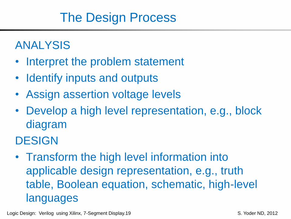
The Design Process
ANALYSIS
• Interpret the problem statement
• Identify inputs and outputs
• Assign assertion voltage levels
• Develop a high level representation, e.g., block
diagram
DESIGN
• Transform the high level information into
applicable design representation, e.g., truth
table, Boolean equation, schematic, high-level
languages
Logic Design: Verilog using Xilinx, 7-Segment Display.20 S. Yoder ND, 2012
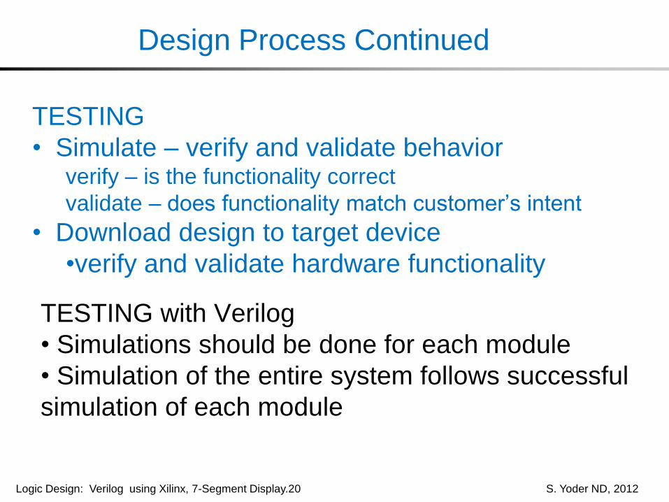
Design Process Continued
TESTING
• Simulate – verify and validate behavior verify – is the functionality correct
validate – does functionality match customer’s intent
• Download design to target device
•verify and validate hardware functionality
TESTING with Verilog
• Simulations should be done for each module
• Simulation of the entire system follows successful
simulation of each module
Logic Design: Verilog using Xilinx, 7-Segment Display.21 S. Yoder ND, 2012
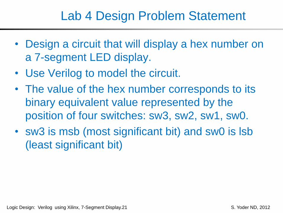
Lab 4 Design Problem Statement
• Design a circuit that will display a hex number on
a 7-segment LED display.
• Use Verilog to model the circuit.
• The value of the hex number corresponds to its
binary equivalent value represented by the
position of four switches: sw3, sw2, sw1, sw0.
• sw3 is msb (most significant bit) and sw0 is lsb
(least significant bit)
Logic Design: Verilog using Xilinx, 7-Segment Display.22 S. Yoder ND, 2012
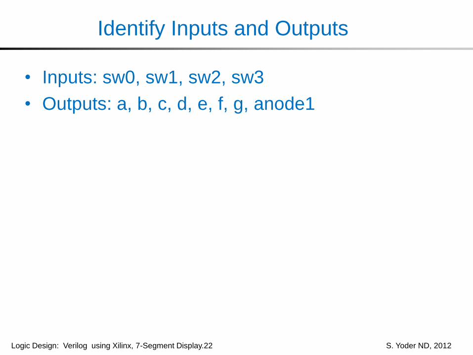
Identify Inputs and Outputs
• Inputs: sw0, sw1, sw2, sw3
• Outputs: a, b, c, d, e, f, g, anode1
Logic Design: Verilog using Xilinx, 7-Segment Display.23 S. Yoder ND, 2012
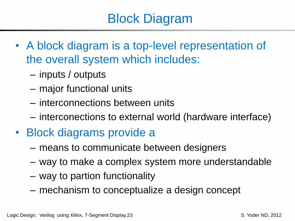
Block Diagram
• A block diagram is a top-level representation of
the overall system which includes:
– inputs / outputs
– major functional units
– interconnections between units
– interconections to external world (hardware interface)
• Block diagrams provide a
– means to communicate between designers
– way to make a complex system more understandable
– way to partion functionality
– mechanism to conceptualize a design concept

Logic Design: Verilog using Xilinx, 7-Segment Display.24 S. Yoder ND, 2012
Block Diagram
BCD to 7-segment
decoder
SW3 SW2 SW1 SW0
0v
5v
a b c d e f g
pull-up resistor
A pull-up resistor forces the voltage at the input to equal 5 v when the
switch is open. The input shouldn’t be left to “float”, which can cause
erratic values.
interface
interface can be subdivided
into additional blocks
Logic Design: Verilog using Xilinx, 7-Segment Display.25 S. Yoder ND, 2012
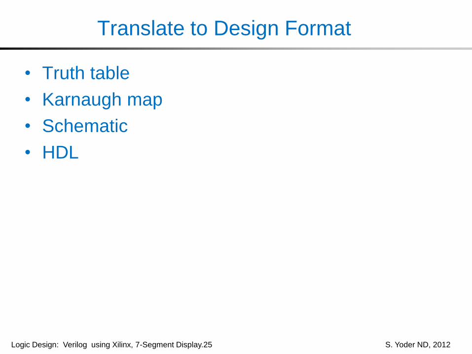
Translate to Design Format
• Truth table
• Karnaugh map
• Schematic
• HDL
Logic Design: Verilog using Xilinx, 7-Segment Display.26 S. Yoder ND, 2012
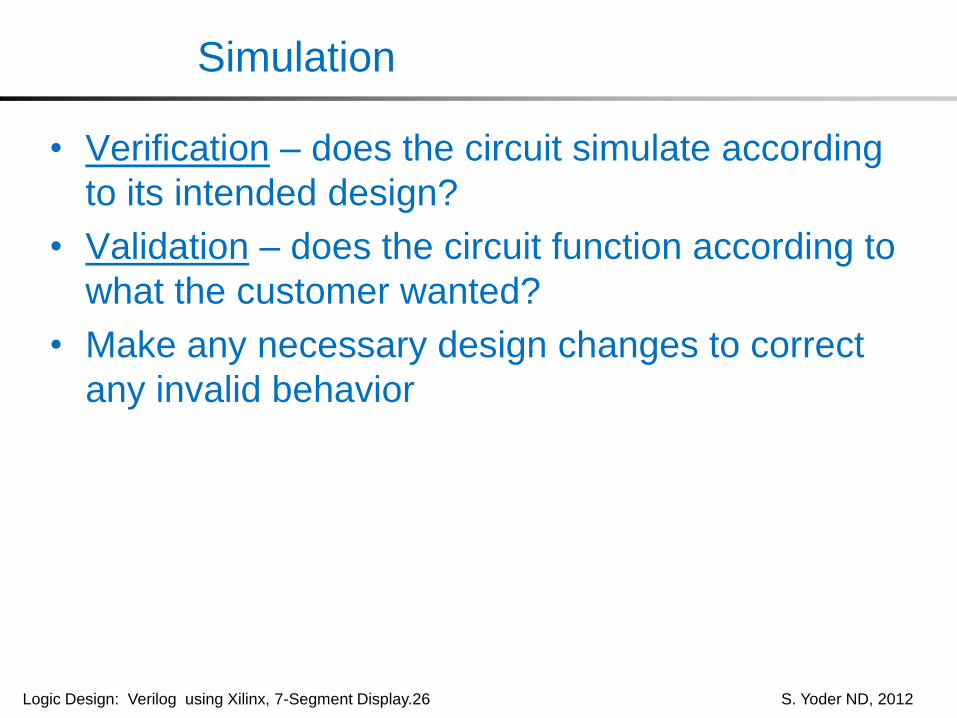
Simulation
• Verification – does the circuit simulate according
to its intended design?
• Validation – does the circuit function according to
what the customer wanted?
• Make any necessary design changes to correct
any invalid behavior

Logic Design: Verilog using Xilinx, 7-Segment Display.27 S. Yoder ND, 2012
Prototype
• Download design to prototype board
• Verify correct functionality
• Repeat necessary design steps to correct any
problems
Logic Design: Verilog using Xilinx, 7-Segment Display.28 S. Yoder ND, 2012
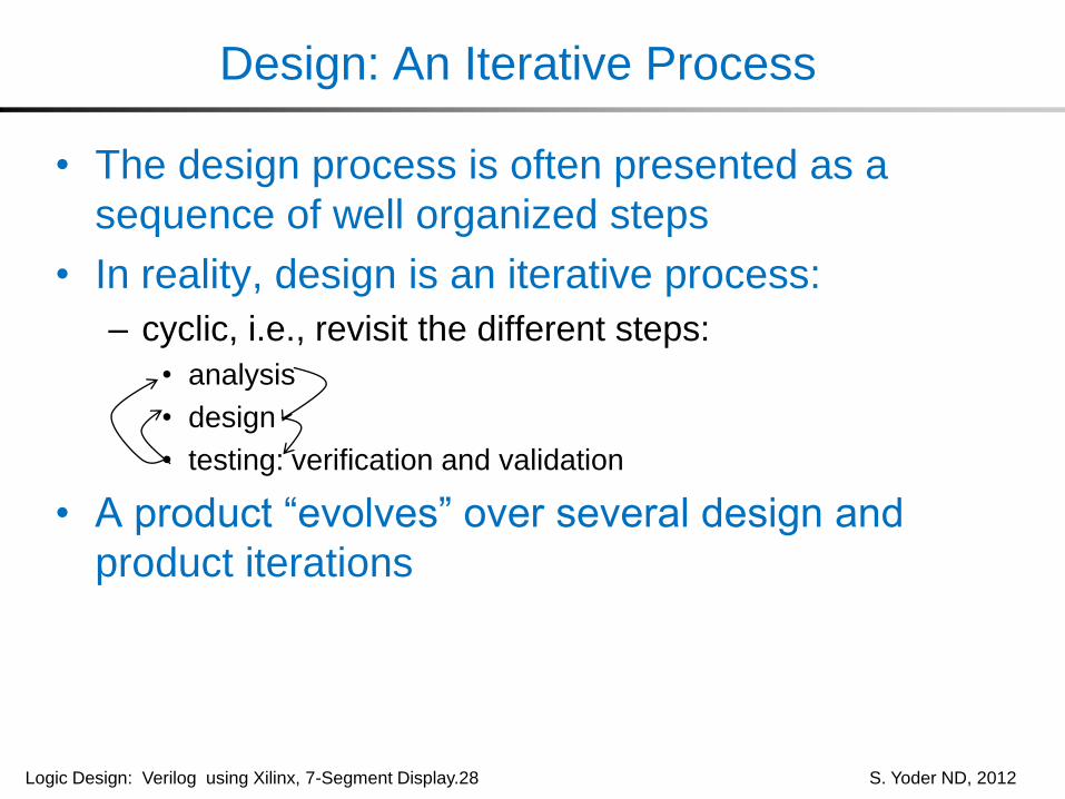
Design: An Iterative Process
• The design process is often presented as a
sequence of well organized steps
• In reality, design is an iterative process:
– cyclic, i.e., revisit the different steps:
• analysis
• design
• testing: verification and validation
• A product “evolves” over several design and
product iterations

Logic Design: Verilog using Xilinx, 7-Segment Display.29 S. Yoder ND, 2012
Homework
Using the Xilinx ISE, create a Verilog model for the g
segment of a seven-segment display, where the value for
the segment must be set to 0 for the LED to light (active
low). Your circuit must display a hex number, i.e., 0, 1 …
8, 9, A, b, c, E, and F. Submit a text file printout of your
Verilog .v file and a printout of your simulation results.