using the ucc28810evm-00, 25-w pfc flyback led converter
TRANSCRIPT

Using the UCC28810EVM-001
User's Guide
Literature Number: SLUU344AFebruary 2009–Revised February 2009

1 Introduction
2 Description
2.1 Typical Applications
2.2 Features
User's GuideSLUU344A–February 2009–Revised February 2009
UCC28810EVM-001 25-W PFC Flyback LED Converter
The UCC28810EVM-001 evaluation module is a 25-W off-line power factor correction (PFC) flybackconverter providing 36 V at 750-mA maximum load current to power a string of lighting class LEDs. ThisEVM allows the customer to evaluate the UCC28810 in an application where LEDs can be used forgeneral illumination applications that require dimming.
This evaluation module uses the UCC28810 LED Lighting Power Controller (TI Literature NumberSLUS865) in a 25-W single stage triac dimmable PFC flyback converter that meets the harmonic currentor power factor requirements set out by various standards. The input accepts a voltage range of 85 VACto 305 VAC. The output provides a constant current of 750 mA, maximum, at up to 36 VDC to drive astring of LEDs. The EVM is designed to be used with a triac dimmer switch, available at any hardware orlighting store, in series with the input voltage to control the lumen output of the LEDs. The converteroperates in critical conduction mode.
This user’s guide provides the schematic, component list, assembly drawing, and test set up necessary toevaluate the UCC28810 for an ac input LED lighting application.
To use an input voltage greater than 265 VAC, it is recommended the user change the fuse, F1, to onerated for at least 300 V at 1 A.
The UCC28810 is suited for use in general lighting applications for low to medium power lumensapplications requiring power factor correction:• Industrial, Commercial, Residential Lighting Fixtures• AC Input General Lighting Applications Using High Brightness (HB) LEDs• Outdoor Lighting: Street, Roadway, Parking, Construction, and Ornamental LED Lighting Fixtures
The UCC28810EVM-001 features include:• 85 VAC to 305 VAC Input Voltage Range• 25 W Output at 750 mA• Single Stage PFC LED Driver• Interfaces With Traditional Wall Dimmers• Critical Conduction Mode• Transformer Zero Energy Detection• Peak Current Limit
UCC28810EVM-001 25-W PFC Flyback LED Converter2 SLUU344A–February 2009–Revised February 2009Submit Documentation Feedback

3 Electrical Performance Specificationswww.ti.com Electrical Performance Specifications
Table 1. UCC28810EVM-001 Electrical Performance SpecificationsSYMBOL PARAMETER TEST CONDITIONS MIN NOM MAX UNITS
Input CharacteristicsVIN Voltage range 85 265 VACfLINE Input frequency 47 63 kHzIIN(max) Input current VIN = 85 VAC, fLINE = 60 Hz, IOUT = full load (1) 0.4 AIIN(no_load) No load input current VIN = 85 VAC, fLINE = 60 Hz, IOUT = 0 A 12 mAOutput CharacteristicsVOUT Output voltage IOUT = full load (1) 29 33 36 VIOUT Output load current 0.7 A
Output current VIN = 85 VAC to 265 VAC, IOUT = full load (1)10 15 %regulation
Output voltage ripple IOUT = full load (1) 2 VppVOUT(OVP) Output over voltage 45 VprotectionSystem CharacteristicsPF Power factor IOUT = full load (1) 0.9η Full load efficiency VIN = 115 VAC 89.5 %THD Total harmonic VIN = 115 VAC, IOUT = full load (1)
24distortionOperating temperature 50 °C
(1) Full load is ten Cree XLamp® 7090 XR-E, white, 700-mA LEDs in series.
SLUU344A–February 2009–Revised February 2009 UCC28810EVM-001 25-W PFC Flyback LED Converter 3Submit Documentation Feedback

4 Schematic
+
+
VD
D
CT
SN
S
RS
T
MR
GN
D
OU
T
IN
FB
/NC
NC
GN
D
+
VS
NS
EA
OU
T
VIN
S
ISN
ST
ZE
GN
D
GD
RV
VD
D
5
2
3 41
Schematic www.ti.com
Figure 1. UCC28810EVM-001 Schematic
UCC28810EVM-001 25-W PFC Flyback LED Converter4 SLUU344A–February 2009–Revised February 2009Submit Documentation Feedback

5 Test Setup
5.1 Test Equipment
5.1.1 AC Voltage Source
5.1.2 Multimeters
5.1.3 Output Load
5.1.4 Oscilloscope
www.ti.com Test Setup
CAUTIONHigh voltage levels are present on the evaluation module whenever it isenergized. Proper precautions must be taken when working with the EVM. Thelarge bulk capacitor across the output terminals must be completely dischargedbefore the EVM can be handled. Serious injury can occur if proper safetyprecautions are not followed.
Refer to Figure 2 for recommended test set up.
The input voltage shall be a transformer isolated variable ac source capable of supplying between 85 VACand 265 VAC, at 60 Hz, at no less than 5 A peak (i.e. Hewlett Packard 6813B 300 VRMS, 1750 VA ACPower Source/Analyzer or VARIAC).
For highest accuracy, the output voltage of the UCC28810EVM-001 shall be monitored by connecting adigital voltmeter, V2, directly across TP21 and TP2 with the positive terminal at TP21 and the negativeterminal at TP2, as shown in Figure 2. A dc current meter, A2, should be placed in series with the load foraccurate current measurements. If using an ac source that does not have an analyzer function, connect avoltmeter, V1, across the input terminals, J1 (Line) and J2 (Neutral) and a current meter, A1, in series withthe line input.
It is recommended that HB LEDs are used for the load. The HB LEDs should be specified for a totalforward voltage of 35 V, typical, at 700 mA of current. Ten Cree XLamp® 7090 XR-E, white, 700-mA LEDsconnected in series was used for the data documented in this user’s guide. Alternatively, a 50-Ω, 50-Wresistor can be used.
A digital or analog oscilloscope with 500-MHz scope probes and a current probe is recommended.
SLUU344A–February 2009–Revised February 2009 UCC28810EVM-001 25-W PFC Flyback LED Converter 5Submit Documentation Feedback

5.1.5 Dimmer
5.1.6 Fan
5.1.7 Recommended Wire Gauge
5.2 Recommended Test Setup
Oscilloscope
A2
-+
A1
-+
V1
+ -
AC
SOURCE
N L
V2
+ -
Optional
DIMMER
Test Setup www.ti.com
A triac dimmer switch, available at hardware or lighting stores, can be inserted in series with the input line.If a dimmer switch is not available, with minor circuit changes, a function generator can be used togenerate a PWM dimming control signal to replicate the triac dimmer.
Forced air cooling is not required.
A minimum of 14 AWG, not longer than two feet total for Line (J1), and Neutral (J2), is recommended. Aminimum of 18 AWG, not longer than one foot total, for the load connection to LED+ (J3) and LED- (J4) isrecommended. Both input and output terminals are designed to accept banana jack connectors.
Figure 2. UCC28810EVM-001 Recommended Test Set Up
UCC28810EVM-001 25-W PFC Flyback LED Converter6 SLUU344A–February 2009–Revised February 2009Submit Documentation Feedback

5.3 List of Test Pointswww.ti.com Test Setup
Table 2. The Functions of Each Test PointsTEST POINTS NAME DESCRIPTION
Via in converter output voltage pad, used for tip and barrel measurement ofTP1 LED+ output voltage rippleTP2 LED- Return of LED string, used for tip and barrel measurement of output rippleTP3 VBIAS Primary side bias to UCC28810 (U1), reference to TP11TP4 Secondary side bias windings, reference to TP20TP5 U2_IN Pin 4 (IN) of TPS71550 (U2), reference to TP20TP6 U1_VINS Pin 3 (VINS) of U1, reference to TP11TP7 U1_VDD Pin 8 (VDD) of U1, reference to TP11TP8 REF5 Pin 5 (OUT) of U2, reference to TP20TP9 Rectified Secondary side bias windings, reference to TP20TP10 EAOUT Pin 2 (EAOUT) of U1, reference to TP11TP11 P_GND Primary side ground
Pin 4 (IN-) of TLV3701 (U5), scaled copy of input voltage waveform, reference toTP12 U5_IN- TP20TP13 Pin 1 (Anode) of CNY17-3S (U3), reference to TP20TP14 U4_2OUT Pin 2 (Cathode) of U3, also pin 7 (2OUT) of TLV272 (U4), reference to TP20TP15 U5_IN+ Pin 3 (IN+) of U5, reference to TP20TP16 U5_OUT Pin 1 (OUT) of U5, reference to TP20TP17 U4_2IN+ Pin 5 (2IN+) of U4, reference to TP20TP18 Loop injection pointTP19 Loop injection point, LED-TP20 S_GND Secondary side groundTP21 LED+ Input to LED stringTP23 U1_GDRV Pin 7 (GDRV) of U1, reference to TP11TP24 U1_ISNS Pin 4 (ISNS) of U1, reference to TP11TP25 U1_TZE Pin 5 (TZE) of U1, reference to TP11
J1 LINE Line input from AC source, standard banana jackJ2 NEUTRAL Neutral input from AC source, standard banana jackJ3 LED+ Output terminal to the LED load string, standard banana jackJ4 LED- Return connection for the LED string, standard banana jack
SLUU344A–February 2009–Revised February 2009 UCC28810EVM-001 25-W PFC Flyback LED Converter 7Submit Documentation Feedback

6 Test Procedure
6.1 Applying Power to the EVM
6.2 Line Regulation
Test Procedure www.ti.com
All tests should use the set up as described in Section 5 of this user’s guide.
WARNINGWARNING HIGH VOLTAGES are present on this evaluation modulewhenever it is energized. Proper precautions must be observedwhenever working with this module. There is an energy storagecapacitor (C6) on this module which must be discharged before theboard can be handled. Serious injury can occur if proper safetyprocedures are not followed.
The following test procedure is recommended primarily for power up and shutting down the EVM. Neverleave a powered EVM unattended for any length of time. The unit should never be handled while power isapplied to it. Always make sure the bulk capacitor has been completely discharged prior to handling theEVM.• Working at an ESD workstation, turn on the ionizer before the EVM is removed from the protective
packaging and power is applied. Electrostatic smock and safety glasses should also be worn. Becausevoltages in excess of 400V may be present on the EVM, do not connect the ground strap from thesmock to the bench.
• Set up the EVM as described in Section 5 of this user’s guide.• Connect the LED string across the output terminals.• Prior to turning on the ac source, set the voltage to 115 VAC. For operation with an input voltage
greater than 265 VAC, but not greater than 305 VAC, change the fuse, F1, to one rated for at least 300V at 1 A
• Monitor the output voltage, V2.• Monitor the output current, A2.
• Apply power to the EVM per Section 6.1• Vary the input voltage from 85 VAC to 265 VAC.• Observe the output current on A2 stays within approximately 10% of the output current measured at
115 VAC.
UCC28810EVM-001 25-W PFC Flyback LED Converter8 SLUU344A–February 2009–Revised February 2009Submit Documentation Feedback
6.3 Output Voltage Ripple
6.4 Dimming
6.5 Equipment Shutdown
www.ti.com Test Procedure
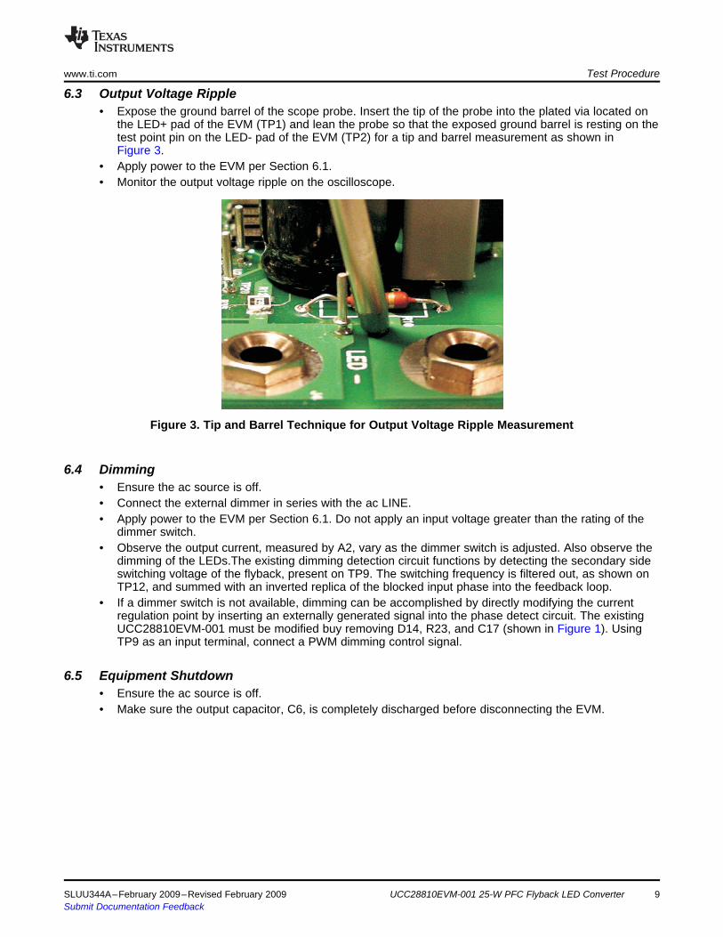
• Expose the ground barrel of the scope probe. Insert the tip of the probe into the plated via located onthe LED+ pad of the EVM (TP1) and lean the probe so that the exposed ground barrel is resting on thetest point pin on the LED- pad of the EVM (TP2) for a tip and barrel measurement as shown inFigure 3.
• Apply power to the EVM per Section 6.1.• Monitor the output voltage ripple on the oscilloscope.
Figure 3. Tip and Barrel Technique for Output Voltage Ripple Measurement
• Ensure the ac source is off.• Connect the external dimmer in series with the ac LINE.• Apply power to the EVM per Section 6.1. Do not apply an input voltage greater than the rating of the
dimmer switch.• Observe the output current, measured by A2, vary as the dimmer switch is adjusted. Also observe the
dimming of the LEDs.The existing dimming detection circuit functions by detecting the secondary sideswitching voltage of the flyback, present on TP9. The switching frequency is filtered out, as shown onTP12, and summed with an inverted replica of the blocked input phase into the feedback loop.
• If a dimmer switch is not available, dimming can be accomplished by directly modifying the currentregulation point by inserting an externally generated signal into the phase detect circuit. The existingUCC28810EVM-001 must be modified buy removing D14, R23, and C17 (shown in Figure 1). UsingTP9 as an input terminal, connect a PWM dimming control signal.
• Ensure the ac source is off.• Make sure the output capacitor, C6, is completely discharged before disconnecting the EVM.
SLUU344A–February 2009–Revised February 2009 UCC28810EVM-001 25-W PFC Flyback LED Converter 9Submit Documentation Feedback
7 Performance Data and Typical Characteristic Curves
7.1 Efficiency
0.80
0.84
0.90
0.94
0.98
0.82
0.86
0.92
0.96
1.00
Effic
ien
cy
-%
EFFICIENCY
vs
LINE VOLTAGE
75 125 225 275
VRMS
- Line Voltage - V
175
0.88
7.2 Power Factor
75 125 225 275
VRMS
- Line Voltage - V
0.90
0.93
0.95
0.96
0.98
175
0.91
0.92
0.94
0.97
Po
we
rF
ac
to
r
POWER FACTOR
vs
LINE VOLTAGE
Performance Data and Typical Characteristic Curves www.ti.com
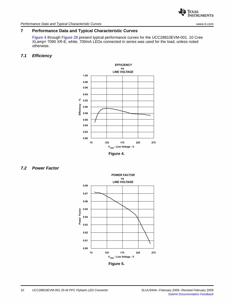
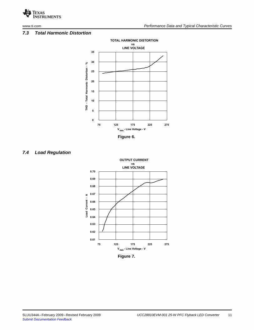
Figure 4 through Figure 28 present typical performance curves for the UCC28810EVM-001. 10 CreeXLamp® 7090 XR-E, white, 700mA LEDs connected in series was used for the load, unless notedotherwise.
Figure 4.
Figure 5.
UCC28810EVM-001 25-W PFC Flyback LED Converter10 SLUU344A–February 2009–Revised February 2009Submit Documentation Feedback
7.3 Total Harmonic Distortion
0
5
20
35
10
15
25
30
TH
D-
To
ta
lH
arm
on
icD
isto
rtio
n-
%
TOTAL HARMONIC DISTORTION
vs
LINE VOLTAGE
75 125 225 275
VRMS
- Line Voltage - V
175
7.4 Load Regulation
0.61
0.63
0.64
0.66
0.68
0.70
0.62
0.65
0.67
0.69
Lo
ad
Cu
rre
nt
-A
OUTPUT CURRENT
vs
LINE VOLTAGE
75 125 225 275
VRMS
- Line Voltage - V
175
www.ti.com Performance Data and Typical Characteristic Curves
Figure 6.
Figure 7.
SLUU344A–February 2009–Revised February 2009 UCC28810EVM-001 25-W PFC Flyback LED Converter 11Submit Documentation Feedback

7.5 Current Harmonics
Current Harmonics at 115VAC
0.00001
0.03778
0.07555
0.11332
0.15108
0.18885
0.22662
1 3 5 7 9 11 13 15 17 19 21 23 25 27 29 31 33 35 37 39
Harmonic Number
Am
pli
tud
e(A
)
Current Harmonics at 115VAC
0
0.005
0.01
0.015
0.02
0.025
0.03
0.035
0.04
0.045
0.05
3 5 7 9 11 13 15 17 19 21 23 25 27 29 31 33 35 37 39
Harmonic Number
Am
pli
tud
e(A
)
Current Harmonics at 230VAC
0
0.005
0.01
0.015
0.02
0.025
0.03
0.035
3 5 7 9 11 13 15 17 19 21 23 25 27 29 31 33 35 37 39
Harmonic Number
Am
plitu
de
(A)
Current Harmonics at 230VAC
0.00000
0.01978
0.03956
0.05934
0.07912
0.09890
0.11868
1 3 5 7 9 11 13 15 17 19 21 23 25 27 29 31 33 35 37 39
Harmonic Number
Am
plitu
de
(A)
Performance Data and Typical Characteristic Curves www.ti.com
Figure 9. VIN = 115 VAC, fLINE = 60 Hz,Figure 8. VIN = 115 VAC, fLINE = 60 Hz,Re-Scaled Without the Fundamental
Figure 11. VIN = 230 VAC, fLINE = 60 Hz,Figure 10. VIN = 230 VAC, fLINE = 60 HzRe-Scaled Without the Fundamental
UCC28810EVM-001 25-W PFC Flyback LED Converter12 SLUU344A–February 2009–Revised February 2009Submit Documentation Feedback

7.6 Input Voltage and Currentwww.ti.com Performance Data and Typical Characteristic Curves
10 Cree XLamp® 7090 XR-E, white, 700-mA LEDs connected in series was used for the load unlessotherwise noted.
Figure 12. VIN = 85 VAC, fLINE = 60 Hz Figure 13. VIN = 115 VAC, fLINE = 60 Hz
Figure 14. VIN = 230 VAC, fLINE = 60 Hz Figure 15. VIN = 265 VAC, fLINE = 60 Hz
SLUU344A–February 2009–Revised February 2009 UCC28810EVM-001 25-W PFC Flyback LED Converter 13Submit Documentation Feedback

Ch. 1 = VIN
, 100V/div.
Ch. 2 = IIN
, 200mA/div.
Ch. 1 = VIN
, 100V/div.
Ch. 2 = IIN
, 200mA/div.
Ch. 1 = VIN
,
100V/div.
Ch. 2 = IIN
,
200mA/div.
Performance Data and Typical Characteristic Curves www.ti.com
Figure 16. Dimmer Set at Full on Position, VIN Figure 17. Dimmer Set at Mid-Range= 115 VAC from Source, fLINE = 60 Hz, Output Dimming Position, VIN = 115 VAC from
Current to LEDs (IOUT) is 552 mA, VOUT = Source, fLINE = 60 Hz, Output Current to LEDs31.36 V (IOUT) is 255 mA, VOUT = 29.57 V
Figure 18. Maximum Dimming Position, VIN =115 VAC from Source, fLINE = 60 Hz, Output
Current to LEDs (IOUT) is 52 mA, VOUT =27.42 V
UCC28810EVM-001 25-W PFC Flyback LED Converter14 SLUU344A–February 2009–Revised February 2009Submit Documentation Feedback

7.7 Output Ripple
Ch. 4 = current ripple, 200mA/div.
Ch. 3 = voltage ripple, 500mV/div.Ch. 3 = voltage ripple, 500mV/div.
Ch. 4 = current ripple, 500mA/div.
Ch. 4 = current ripple, 20mA/div.
Ch. 3 = voltage ripple, 200mV/div.
www.ti.com Performance Data and Typical Characteristic Curves
Figure 19. Output Voltage and Current Figure 20. Output Voltage and CurrentRipple, VIN = 115 VAC, fLINE = 60 Hz, No Ripple, VIN = 115 VAC, fLINE = 60 Hz, Dimmer
Set at Mid-Range Dimming Position, VOUT =Dimmer, VOUT = 31.68 V, IOUT = 0.655 A29.41 V, IOUT = 0.228 A
Figure 21. Output Voltage and CurrentRipple, VIN = 115 VAC, fLINE = 60 Hz, DimmerSet at Maximum Dimming Position, VOUT =
27.55 V, IOUT = 0.058 A
SLUU344A–February 2009–Revised February 2009 UCC28810EVM-001 25-W PFC Flyback LED Converter 15Submit Documentation Feedback

7.8 Turn-On WaveformPerformance Data and Typical Characteristic Curves www.ti.com
Output voltage turn-on waveform. Unless otherwise noted, 10 Cree XLamp® 7090 XR-E, white, 700mALEDs connected in series was used for the load.
Figure 22. VIN = 115 VAC, fLINE = 60 Hz, No Figure 23. VIN = 115 VAC, fLINE = 60 Hz, NoDimmer, No Load. Ch. 1 = VOUT, 10V/div. VOUTDimmer, Ch. 1 = VOUT, 10V/div. VOUT = 32.2 V
= 44.8 V
Figure 24. VIN = 115 VAC, fLINE = 60 Hz,Dimmer Set at Maximum Dimming Position,
Ch. 1 = VOUT, 10V/div. VOUT = 27.42 V
UCC28810EVM-001 25-W PFC Flyback LED Converter16 SLUU344A–February 2009–Revised February 2009Submit Documentation Feedback

7.9 Dimming Detection:
Ch. 3 = TP17, 2.16V at 2V/div.
Ch. 4 = IOUT
, 1A/div.
Ch. 2 = TP16, 5V/div.
Ch.1 = TP12, 1V/div.
Ch. 3 = TP17, 2.12V at 2V/div.
Ch. 4 = IOUT
, 1A/div.
Ch. 2 = TP16, 5V/div.
Ch.1 = TP12, 1V/div.
Ch. 3 = TP17, 2.16V at 2V/div.
Ch. 4 = IOUT
, 1A/div.
Ch. 2 = TP16, 5V/div.
Ch.1 = TP12, 1V/div.
Ch. 3 = TP17, 2.44V at 2V/div.
Ch. 4 = IOUT
, 1A/div.
Ch. 2 = TP16, 5V/div.
Ch.1 = TP12, 1V/div.
www.ti.com Performance Data and Typical Characteristic Curves
Figure 25. Triac Dimming Detection Signals, Figure 26. Triac Dimming Detection Signals,VIN = 115 VAC, fLINE = 60 Hz, VOUT = 31.66 V, VIN = 115 VAC, fLINE = 60 Hz, VOUT = 31.19 V,
IOUT = 0.653 A, (no dimmer on the input) IOUT = 0.552 A, (dimmer set at full on position)
Figure 27. Triac Dimming Detection Signals, Figure 28. Triac Dimming Detection Signals,VIN = 115 VAC, fLINE = 60 Hz, VOUT = 29.54 V, VIN = 115 VAC, fLINE = 60 Hz, VOUT = 27.44 V,
IOUT = 0.266 A, (dimmer set at mid-range IOUT = 0.058 A, (dimmer set at maximumdimming position) dimming position)
SLUU344A–February 2009–Revised February 2009 UCC28810EVM-001 25-W PFC Flyback LED Converter 17Submit Documentation Feedback
8 EVM Assembly Drawing and PCB layoutEVM Assembly Drawing and PCB layout www.ti.com
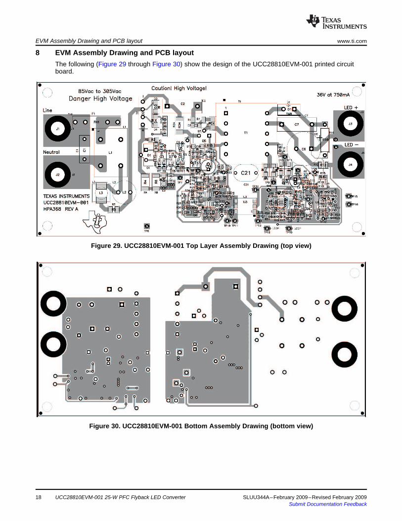
The following (Figure 29 through Figure 30) show the design of the UCC28810EVM-001 printed circuitboard.
Figure 29. UCC28810EVM-001 Top Layer Assembly Drawing (top view)
Figure 30. UCC28810EVM-001 Bottom Assembly Drawing (bottom view)
UCC28810EVM-001 25-W PFC Flyback LED Converter18 SLUU344A–February 2009–Revised February 2009Submit Documentation Feedback

9 List of Materialswww.ti.com List of Materials
Table 3. The EVM Components List According to the Schematic Shown in Figure 1REF DES COUNT DESCRIPTION MFR PART NUMBER
C1 Capacitor, polypropylene, 47 nF, X2, 305 VAC, ±20%, Epcos B32921A2473M or1 0.236 x 0.512 inch B32921C3473MC2 Capacitor, polypropylene, 0.10 µF, X2, 305 VAC, ±20%, Epcos B32922C3104M1 0.200 x 0.709 inchC3 1 Capacitor, ceramic, 1000 pF, 200 V, X7R, ±10%, 1206 Std StdC4, C26 2 Capacitor, ceramic, 0.047 µF, 50 V, X7R, ±10%, 0805 Std StdC5, C11, C15, Capacitor, ceramic, 1 nF, 50 V, X7R, ±10%, 0805 Std Std6C22, C29, C32C6 Capacitor, alum.electrolytic, 1000 µF, 50 V, ±20%, 16 x Panasonic EEU-FM1H1021 25 mmC7 Capacitor, metal Poly, 2.2 µF, 100 VDC, ±10%, 0.709 x Vishay 2222 373 212251 0.236 inchC8, C10, C16, Capacitor, ceramic, 1 µF, 50 V, X7R, ±10%, 0805 Std Std5C30, C31C9 Capacitor, aluminum, 33 µF, 35 V, ±20%, 0.200 x 0.435 United ChemiCon EKY-1 inch 350ELL330ME11DC12, C23, C24, Capacitor, ceramic, 0.1 µF, 50 V, X7R, ±10%, 0805 Std Std5C25, C28C13 1 Capacitor, ceramic, 22 µF, 25 V, X5R, ±20%, 1210 Std StdC14 1 Capacitor, aluminum, 100 µF, 25 V, ±20%, 0.200 inch Nichicon UHE1E101MEDC17, C27 2 Capacitor, ceramic, 10 nF, 50 V, X7R, ±10%, 0805 Std StdC18, C19 Capacitor, ceramic, 47 pF, 100 V, C0G, NP0 , ±10%, Std Std2 0805C20 1 Capacitor, ceramic, 10 µF, 10 V, X7R, ±10%, 1206 Std StdC21 Capacitor, ceramic disc, 1000 pF, 250 V, Y1, ±20%, Panasonic ECK-ANA102MB1 0.394 x 0.315 inchC33 Capacitor, ceramic, not populated, 50 V, X7R, ±10%, Std Std0 0805D1 1 Diode, power rectifier, 8 A, 400 V, TO-220AC ON Semiconductor MUR840GD2 1 Diode, bridge rectifier, 1.5 A, 600 V, 0.580 x 0.145 inch Diodes Inc. KBP06GD3, D4 2 Diode, switching, 1 A, 600 V, SMA Diodes Inc. RS1J-13-FD5 Diode, switching, Dual, 200 mA, 70 V, SOT-23 Fairchild BAV701 SemiconductorD6 1 Diode, rectifier, 1 A, 1000 V, SMA Diodes Inc. US1M-13-FD7 1 Diode, Zener, 18 V, 350 mW, SOT-23 Diodes Inc. BZX84C18T-7D8 1 Diode, Zener, 12 V, 350 mW, SOT-23 Diodes Inc. BZX84C12-7-FD9 0 not populated, SMAD10, D11, D12, Diode, ultra fast rectifier, 1 A, 200 V, SMA ON Semiconductor MURA120T35D13, D14D15 1 Diode, Zener, 350 mA, 15 V, SOT-23 Diodes Inc. MMBZ5245B-7-FD16 1 Diode, Schottky, 1.5 A, 25 V, SMA Vishay BYS10-25-E3/TRD17 1 Diode, Schottky, 200 mA, 30 V, SOT-23 Vishay-Liteon BAT54D18 Diode, switching, 200 mA, 85 V, 350 mW, SOT-23 Fairchild BAS161 SemiconductorD19 0 not populated, SOT-23
SLUU344A–February 2009–Revised February 2009 UCC28810EVM-001 25-W PFC Flyback LED Converter 19Submit Documentation Feedback

List of Materials www.ti.com
Table 3. The EVM Components List According to the Schematic Shown in Figure 1 (continued)REF DES COUNT DESCRIPTION MFR PART NUMBER
F1 1 Fuse, slow, 1 A, 250 V, 5 x 20 mm Std StdL1 Inductor, common mode, 2.2 mH, 1.5 A, 0.590 x 0.893 Panasonic ELF-18D228F1 inchL2 Inductor, power, 1 mH, 0.6 A, 1.45 W, 0.430 x 0.450 Coilcraft RFB1010-102L1 inchL3 1 Inductor, SMT, 33 µH, 1.31 A, 0.166 W, 0.300 sq inch Coiltronics DR73-330-RQ1 1 MOSFET, N-channel, 600 V, 2 A, 4.5 W, TO-220V Toshiba 2SK3767Q2, Q3, Q7, Bipolar, NPN, 40 V, 200 mA, 330 mW, SOT-23 Infineon MMBT3904LT14Q9 TechnologiesQ4 Bipolar, NPN, 80 V, 500 mA, 350 mW, SOT-23 Fairchild MMBTA061 SemiconductorQ5 MOSFET, N-channel, 800 V, 0.9 W, TO-220V Infineon SPA06N80C31 TechnologiesQ6 1 Transistor, PNP, -60 V, -600 mA, 225 mW, SOT-23 ON Semiconductor MMBT2907ALT1Q8 Bipolar, PNP, 40 V, 200 mA, 250 mW, SOT-23 Infineon MMBT3906LT11 TechnologiesR1 1 Resistor, chip, 15 kΩ, 1/2 W, ±5%, 2010 Std StdR2, R3 2 Resistor, chip, 499 kΩ 1/4 W, ±1%, 1206 Std StdR4, R8 0 Resistor, chip, not populated, 1 W, ±1%, 2512 Std StdR5 (1) 1 Resistor, chip, 33 Ω, 1/2 W, ±5%, anti-surge, 1210 Panasonic ERJ-P14J330UR6, R7, R9, Resistor, chip, 1.00 kΩ 1/8 W, ±1%, 0805 Std Std6R11, R36, R43R10 Resistor, metal film, 51 kΩ, 1 W, ±5%, 0.130 x 0.600 BC Components PR01000105102JR51 inch 00R12 1 Resistor, chip, 0.39 Ω, 1/2 W, ±1%, 1210 Std StdR13, R17 2 Resistor, chip, 1 MΩ, 1/4 W, ±5%, 1206 Std StdR14, R19 0 Resistor, chip, not populated, 1/8 W, ±1%, 0805 Std StdR15, R24 2 Resistor, chip, 10.0 Ω, 1/4 W, ±1%, 1206 Std StdR16 1 Resistor, chip, 20.0 Ω, 1/4 W, ±1%, 1206 Std StdR18 1 Resistor, chip, 3.01 kΩ, 1/8 W, ±1%, 0805 Std StdR20 1 Resistor, chip, 180 kΩ, 1/8 W, ±1%, 0805 Std StdR21 1 Resistor, chip, 11.3 kΩ, 1/8 W, ±1%, 0805 Std StdR22, R26, R30, Resistor, chip, 100 kΩ, 1/8 W, ±1%, 0805 Std Std6R35, R38, R39R23 1 Resistor, chip, 1.00 MΩ, 1/10 W, ±1%, 0603 Std StdR25, R31, R52 3 Resistor, chip, 10.0 kΩ, 1/8 W, ±1%, 0805 Std StdR27 1 Resistor, chip, 22.0 kΩ, 1/10 W, ±1%, 0603 Std StdR28 1 Resistor, chip, 100 Ω, 1/8 W, ±1%, 0805 Std StdR29, R50 2 Resistor, chip, 20.0 kΩ, 1/8 W, ±1%, 0805 Std StdR32 1 Resistor, chip, 4.99 kΩ, 1/8 W, ±1%, 0805 Std StdR33 1 Resistor, axial, 330 Ω, 1/2 W, ±5%, 0.300 x 0.100 inch Panasonic ERD-S2TJ331VR34 1 Resistor, chip, 0.62 Ω, 1 W, ±1%, 2512 Panasonic ERJ-1TRQFR62U
(1) All other components can be substituted with equivalent MFG's components.
20 UCC28810EVM-001 25-W PFC Flyback LED Converter SLUU344A–February 2009–Revised February 2009Submit Documentation Feedback

www.ti.com List of Materials
Table 3. The EVM Components List According to the Schematic Shown in Figure 1 (continued)REF DES COUNT DESCRIPTION MFR PART NUMBER
R37, R48 2 Resistor, chip, 249 kΩ, 1/8 W, ±1%, 0805 Std StdR40 0 Resistor, chip, not populated, 1/10 W, ±1%, 0603 Std StdR41 1 Resistor, chip, 0 Ω, 1/10 W, ±5%, 0603 Std StdR42 1 Resistor, chip, 13.3 kΩ, 1/10 W, ±1%, 0603 Std StdR44 1 Resistor, chip, 5.76 kΩ, 1/10 W, ±1%, 0603 Std StdR45 1 Resistor, chip, 24.9 kΩ, 1/10 W, ±1%, 0603 Std StdR46 1 Resistor, chip, 200 kΩ, 1/10 W, ±1%, 0603 Std StdR47 1 Resistor, chip, 365 kΩ, 1/10 W, ±1%, 0603 Std StdR49 1 Resistor, chip, 330 Ω, 1/10 W, ±1%, 0603 Std StdR51 1 Resistor, chip, 49.9 Ω, 1/10 W, ±1%, 0603 Std StdT1 Xfmr., EF25, 240 µH, N87, 1.122 x 1.161 inch Vitec or GCi 58P6930 (Vitec) or1 G084146LF (GCi)U1 (1) 1 LED lighting power controller, SO-8 Texas Instruments UCC28810DU2 (1) 50 mA, 24 Vin, 5 Vout LDO linear regulator, SOP-5 Texas Instruments TPS71550DCKR1 (DCK)U3 1 Optocoupler, 70 V, 100% CTR, SO-6 Lite-On Inc. CNY17-3SU4 (1) 1 Precision dual operational amplifiers, SO-8 Texas Instruments TLV272CDU5 (1) Nanopower push-pull output comparators, SOT-23-5 Texas Instruments TLV3701CDBV1 (DBV)U6 (1) 1 Progammable-delay supervisory circuit, SOT-23-6 Texas Instruments TPS3808G50DBVRVR1 (1) 1 Shunt voltage reference, 2.048 V, ±1%, SOT-23 Texas Instruments LM4040D20IDBZR-- 1 PCB, 6.4 In x 3 In x 0.062 In Any HPA368
SLUU344A–February 2009–Revised February 2009 UCC28810EVM-001 25-W PFC Flyback LED Converter 21Submit Documentation Feedback

List of Materials www.ti.com
EVALUATION BOARD/KIT IMPORTANT NOTICETexas Instruments (TI) provides the enclosed product(s) under the following conditions:This evaluation board/kit is intended for use for ENGINEERING DEVELOPMENT, DEMONSTRATION, OR EVALUATIONPURPOSES ONLY and is not considered by TI to be a finished end-product fit for general consumer use. Persons handling theproduct(s) must have electronics training and observe good engineering practice standards. As such, the goods being provided arenot intended to be complete in terms of required design-, marketing-, and/or manufacturing-related protective considerations,including product safety and environmental measures typically found in end products that incorporate such semiconductorcomponents or circuit boards. This evaluation board/kit does not fall within the scope of the European Union directives regardingelectromagnetic compatibility, restricted substances (RoHS), recycling (WEEE), FCC, CE or UL, and therefore may not meet thetechnical requirements of these directives or other related directives.Should this evaluation board/kit not meet the specifications indicated in the User’s Guide, the board/kit may be returned within 30days from the date of delivery for a full refund. THE FOREGOING WARRANTY IS THE EXCLUSIVE WARRANTY MADE BYSELLER TO BUYER AND IS IN LIEU OF ALL OTHER WARRANTIES, EXPRESSED, IMPLIED, OR STATUTORY, INCLUDINGANY WARRANTY OF MERCHANTABILITY OR FITNESS FOR ANY PARTICULAR PURPOSE.The user assumes all responsibility and liability for proper and safe handling of the goods. Further, the user indemnifies TI from allclaims arising from the handling or use of the goods. Due to the open construction of the product, it is the user’s responsibility totake any and all appropriate precautions with regard to electrostatic discharge.EXCEPT TO THE EXTENT OF THE INDEMNITY SET FORTH ABOVE, NEITHER PARTY SHALL BE LIABLE TO THE OTHERFOR ANY INDIRECT, SPECIAL, INCIDENTAL, OR CONSEQUENTIAL DAMAGES.TI currently deals with a variety of customers for products, and therefore our arrangement with the user is not exclusive.TI assumes no liability for applications assistance, customer product design, software performance, or infringement ofpatents or services described herein.Please read the User’s Guide and, specifically, the Warnings and Restrictions notice in the User’s Guide prior to handling theproduct. This notice contains important safety information about temperatures and voltages. For additional information on TI’senvironmental and/or safety programs, please contact the TI application engineer or visit www.ti.com/esh.No license is granted under any patent right or other intellectual property right of TI covering or relating to any machine, process, orcombination in which such TI products or services might be or are used.
FCC WarningThis evaluation board/kit is intended for use for ENGINEERING DEVELOPMENT, DEMONSTRATION, OR EVALUATIONPURPOSES ONLY and is not considered by TI to be a finished end-product fit for general consumer use. It generates, uses, andcan radiate radio frequency energy and has not been tested for compliance with the limits of computing devices pursuant to part 15of FCC rules, which are designed to provide reasonable protection against radio frequency interference. Operation of thisequipment in other environments may cause interference with radio communications, in which case the user at his own expensewill be required to take whatever measures may be required to correct this interference.
EVM WARNINGS AND RESTRICTIONSIt is important to operate this EVM within the input voltage range of 85 VAC to 265 VAC and the maximum output current of750 mA.Exceeding the specified input range may cause unexpected operation and/or irreversible damage to the EVM. If there arequestions concerning the input range, please contact a TI field representative prior to connecting the input power.Applying loads outside of the specified output range may result in unintended operation and/or possible permanent damage to theEVM. Please consult the EVM User's Guide prior to connecting any load to the EVM output. If there is uncertainty as to the loadspecification, please contact a TI field representative.During normal operation, some circuit components may have case temperatures greater than 50°C. The EVM is designed tooperate properly with certain components above as long as the input and output ranges are maintained. These components includebut are not limited to linear regulators, switching transistors, pass transistors, and current sense resistors. These types of devicescan be identified using the EVM schematic located in the EVM User's Guide. When placing measurement probes near thesedevices during operation, please be aware that these devices may be very warm to the touch.
Mailing Address: Texas Instruments, Post Office Box 655303, Dallas, Texas 75265Copyright © 2009, Texas Instruments Incorporated
22 UCC28810EVM-001 25-W PFC Flyback LED Converter SLUU344A–February 2009–Revised February 2009Submit Documentation Feedback

IMPORTANT NOTICETexas Instruments Incorporated and its subsidiaries (TI) reserve the right to make corrections, modifications, enhancements, improvements,and other changes to its products and services at any time and to discontinue any product or service without notice. Customers shouldobtain the latest relevant information before placing orders and should verify that such information is current and complete. All products aresold subject to TI’s terms and conditions of sale supplied at the time of order acknowledgment.TI warrants performance of its hardware products to the specifications applicable at the time of sale in accordance with TI’s standardwarranty. Testing and other quality control techniques are used to the extent TI deems necessary to support this warranty. Except wheremandated by government requirements, testing of all parameters of each product is not necessarily performed.TI assumes no liability for applications assistance or customer product design. Customers are responsible for their products andapplications using TI components. To minimize the risks associated with customer products and applications, customers should provideadequate design and operating safeguards.TI does not warrant or represent that any license, either express or implied, is granted under any TI patent right, copyright, mask work right,or other TI intellectual property right relating to any combination, machine, or process in which TI products or services are used. Informationpublished by TI regarding third-party products or services does not constitute a license from TI to use such products or services or awarranty or endorsement thereof. Use of such information may require a license from a third party under the patents or other intellectualproperty of the third party, or a license from TI under the patents or other intellectual property of TI.Reproduction of TI information in TI data books or data sheets is permissible only if reproduction is without alteration and is accompaniedby all associated warranties, conditions, limitations, and notices. Reproduction of this information with alteration is an unfair and deceptivebusiness practice. TI is not responsible or liable for such altered documentation. Information of third parties may be subject to additionalrestrictions.Resale of TI products or services with statements different from or beyond the parameters stated by TI for that product or service voids allexpress and any implied warranties for the associated TI product or service and is an unfair and deceptive business practice. TI is notresponsible or liable for any such statements.TI products are not authorized for use in safety-critical applications (such as life support) where a failure of the TI product would reasonablybe expected to cause severe personal injury or death, unless officers of the parties have executed an agreement specifically governingsuch use. Buyers represent that they have all necessary expertise in the safety and regulatory ramifications of their applications, andacknowledge and agree that they are solely responsible for all legal, regulatory and safety-related requirements concerning their productsand any use of TI products in such safety-critical applications, notwithstanding any applications-related information or support that may beprovided by TI. Further, Buyers must fully indemnify TI and its representatives against any damages arising out of the use of TI products insuch safety-critical applications.TI products are neither designed nor intended for use in military/aerospace applications or environments unless the TI products arespecifically designated by TI as military-grade or "enhanced plastic." Only products designated by TI as military-grade meet militaryspecifications. Buyers acknowledge and agree that any such use of TI products which TI has not designated as military-grade is solely atthe Buyer's risk, and that they are solely responsible for compliance with all legal and regulatory requirements in connection with such use.TI products are neither designed nor intended for use in automotive applications or environments unless the specific TI products aredesignated by TI as compliant with ISO/TS 16949 requirements. Buyers acknowledge and agree that, if they use any non-designatedproducts in automotive applications, TI will not be responsible for any failure to meet such requirements.Following are URLs where you can obtain information on other Texas Instruments products and application solutions:Products ApplicationsAmplifiers amplifier.ti.com Audio www.ti.com/audioData Converters dataconverter.ti.com Automotive www.ti.com/automotiveDLP® Products www.dlp.com Broadband www.ti.com/broadbandDSP dsp.ti.com Digital Control www.ti.com/digitalcontrolClocks and Timers www.ti.com/clocks Medical www.ti.com/medicalInterface interface.ti.com Military www.ti.com/militaryLogic logic.ti.com Optical Networking www.ti.com/opticalnetworkPower Mgmt power.ti.com Security www.ti.com/securityMicrocontrollers microcontroller.ti.com Telephony www.ti.com/telephonyRFID www.ti-rfid.com Video & Imaging www.ti.com/videoRF/IF and ZigBee® Solutions www.ti.com/lprf Wireless www.ti.com/wireless
Mailing Address: Texas Instruments, Post Office Box 655303, Dallas, Texas 75265Copyright © 2009, Texas Instruments Incorporated