90w single pfc flyback adapter
TRANSCRIPT
7/27/2019 90W Single PFC Flyback Adapter
http://slidepdf.com/reader/full/90w-single-pfc-flyback-adapter 1/38
POWER ELECTRONICSR & D LABORATORY
90-W ADAPTER WITH VARIABLE-
FREQUENCY SINGLE-STAGE PFC
FLYBACK CONVERTER
April, 2002
7/27/2019 90W Single PFC Flyback Adapter
http://slidepdf.com/reader/full/90w-single-pfc-flyback-adapter 2/38
POWER ELECTRONICSR & D LABORATORY
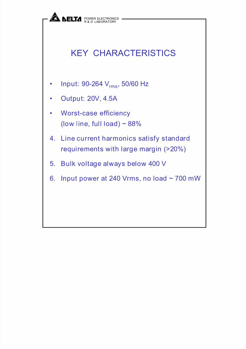
KEY CHARACTERISTICS
• Input: 90-264 Vrms, 50/60 Hz
• Output: 20V, 4.5A
• Worst-case efficiency
(low l ine, full load) ~ 88%
4. Line current harmonics satisfy standardrequirements with large margin (>20%)
5. Bulk voltage always below 400 V
6. Input power at 240 Vrms, no load ~ 700 mW

7/27/2019 90W Single PFC Flyback Adapter
http://slidepdf.com/reader/full/90w-single-pfc-flyback-adapter 3/38
POWER ELECTRONICSR & D LABORATORY
PRESENTATION OUTLINE
• Circuit diagram
• Circuit operation
• Experimental circuit
• Measurements
• Experimental waveforms
• Summary
7/27/2019 90W Single PFC Flyback Adapter
http://slidepdf.com/reader/full/90w-single-pfc-flyback-adapter 4/38
POWER ELECTRONICSR & D LABORATORY
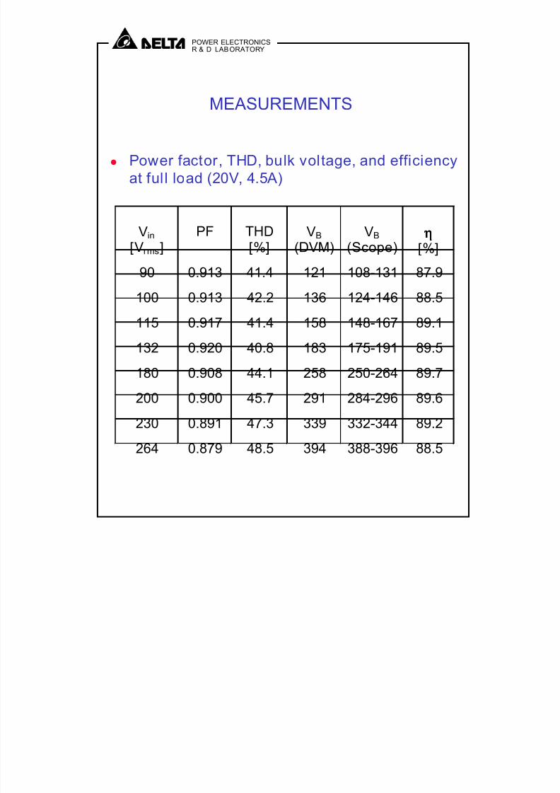
MEASUREMENTS
Vin
[Vrms]PF THD
[%]VB
(DVM)VB
(Scope)ηηηη
[%]
90 0.913 41.4 121 108-131 87.9
100 0.913 42.2 136 124-146 88.5
115 0.917 41.4 158 148-167 89.1
132 0.920 40.8 183 175-191 89.5
180 0.908 44.1 258 250-264 89.7
200 0.900 45.7 291 284-296 89.6
230 0.891 47.3 339 332-344 89.2264 0.879 48.5 394 388-396 88.5
! Power factor, THD, bulk voltage, and efficiency
at ful l load (20V, 4.5A)
7/27/2019 90W Single PFC Flyback Adapter
http://slidepdf.com/reader/full/90w-single-pfc-flyback-adapter 5/38
POWER ELECTRONICSR & D LABORATORY
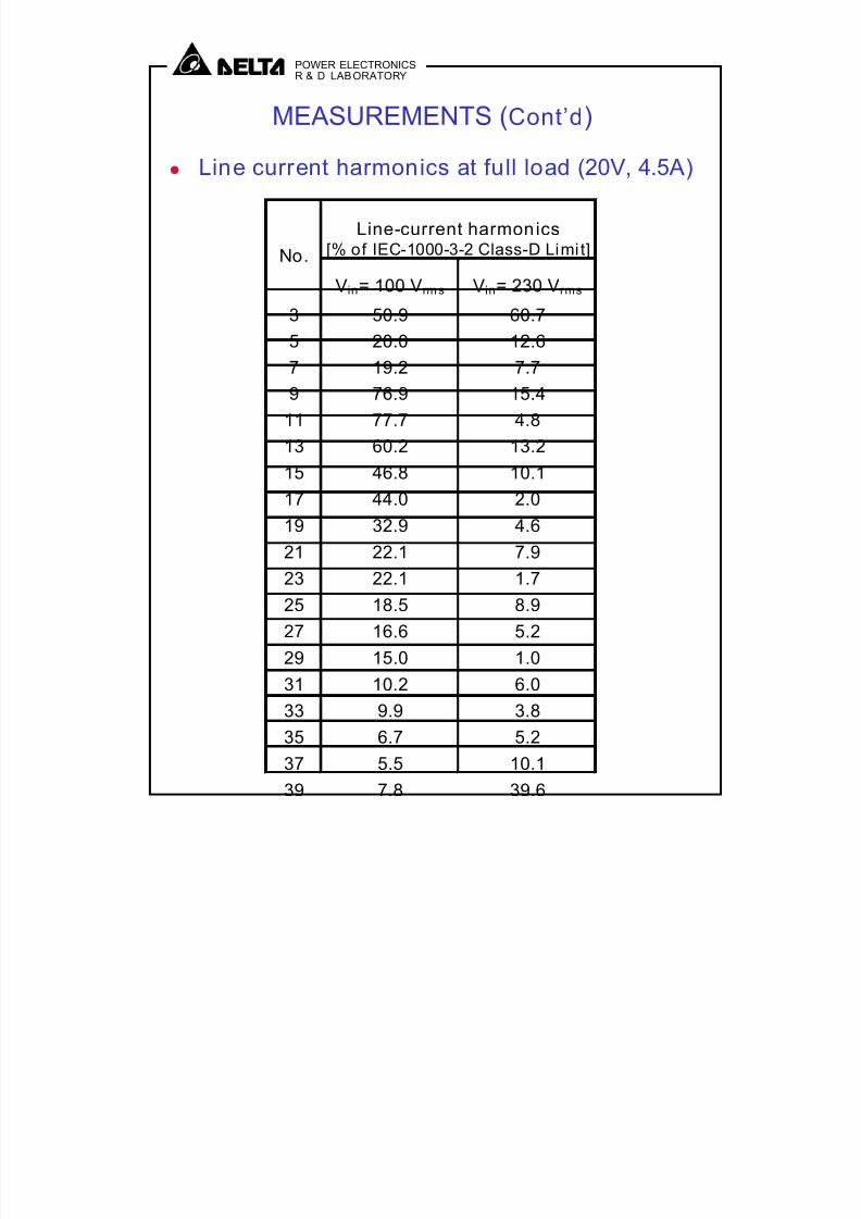
No.
Line-current harmonics[% of IEC-1000-3-2 Class-D Limi t]
Vin= 100 Vrm s Vin= 230 Vrms
3 50.9 60.7
5 20.0 12.6
7 19.2 7.7
9 76.9 15.4
11 77.7 4.8
13 60.2 13.2
15 46.8 10.1
17 44.0 2.0
19 32.9 4.6
21 22.1 7.9
23 22.1 1.7
25 18.5 8.9
27 16.6 5.2
29 15.0 1.031 10.2 6.0
33 9.9 3.8
35 6.7 5.2
37 5.5 10.1
39 7.8 39.6
MEASUREMENTS (Cont’d)
! Line current harmonics at full load (20V, 4.5A)
7/27/2019 90W Single PFC Flyback Adapter
http://slidepdf.com/reader/full/90w-single-pfc-flyback-adapter 6/38
POWER ELECTRONICSR & D LABORATORY
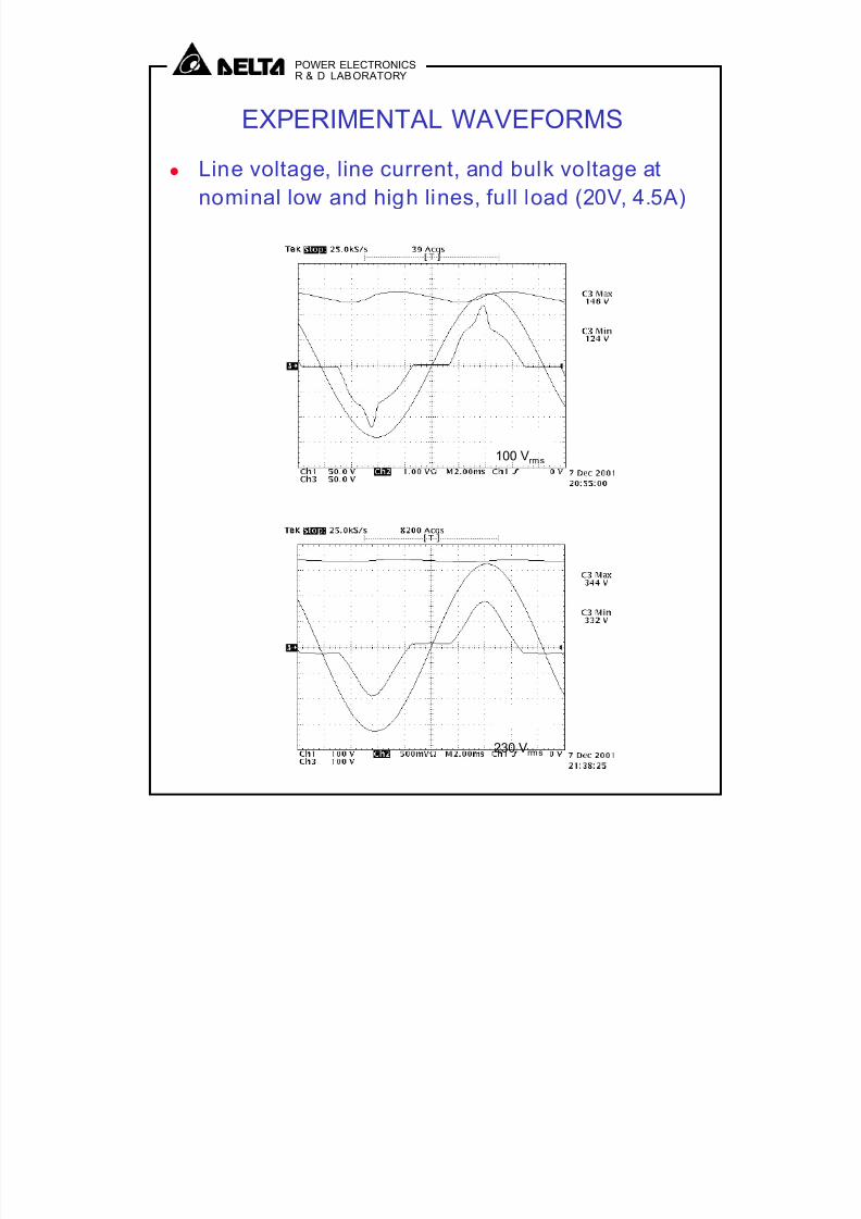
EXPERIMENTAL WAVEFORMS
! Line voltage, line current, and bulk voltage atnominal low and high lines, full load (20V, 4.5A)
230 Vrms
100 Vrms
7/27/2019 90W Single PFC Flyback Adapter
http://slidepdf.com/reader/full/90w-single-pfc-flyback-adapter 7/38
POWER ELECTRONICSR & D LABORATORY
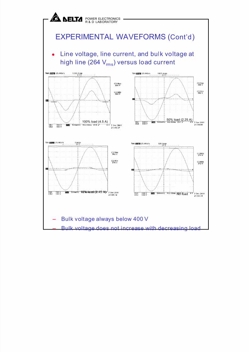
EXPERIMENTAL WAVEFORMS (Cont’d)
! Line voltage, line current, and bulk voltage at
high line (264 Vrms) versus load current
100% load (4.5 A)
10% load (0.45 A)
50% load (2.25 A)
No load
– Bulk voltage always below 400 V
– Bulk voltage does not increase with decreasing load
7/27/2019 90W Single PFC Flyback Adapter
http://slidepdf.com/reader/full/90w-single-pfc-flyback-adapter 8/38
POWER ELECTRONICSR & D LABORATORY
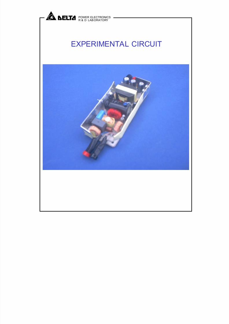
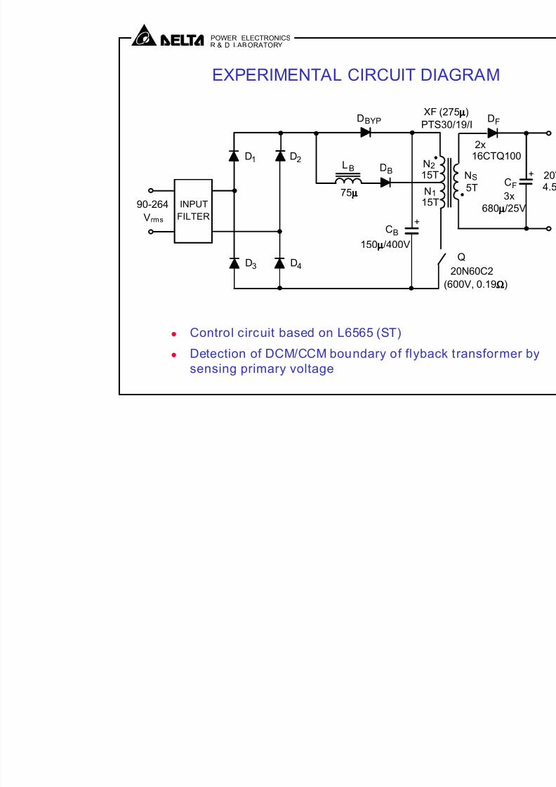
EXPERIMENTAL CIRCUIT

7/27/2019 90W Single PFC Flyback Adapter
http://slidepdf.com/reader/full/90w-single-pfc-flyback-adapter 9/38
POWER ELECTRONICSR & D LABORATORY
SUMMARY
• Comparison with corresponding
2-stage PFC flyback adapter
– Similar performance
– Smaller size
– Lower cost
• S2PFC flyback technology can be used for
adapters from 70 W to ~ 120 W
7/27/2019 90W Single PFC Flyback Adapter
http://slidepdf.com/reader/full/90w-single-pfc-flyback-adapter 10/38
POWER ELECTRONICSR & D LABORATORY
CIRCUIT DIAGRAM
! S2PFC flybac
center-tappe
(US Patent N
RiP
v in
NS
LB DF
i SW
vin(rec)CF
+
i P
SW
i LB
RL
+
Vo
i S
Cin
iSWRiP.
_
+
d
SwitchDriver
Comparator C
R
S Q
Latch
D
_
+
_
+
N1 N2+ = NP
VB CB
+
N2
N1
RiS
B
Delay
DT
A
Zero-Crossing Detector
iSRiS.
DD
VREF
Z1
Z2
_
+
EA
vEA
+
R1
R2
O u t p u t - V o l t a g e
D i v
i d e r
Comparator B
Comparator A
T1
! Flyback tran
DCM/CCM bo
Variable s
(No clock)
Detection
by sensin
Switch tur
crosses z
Bulk volta
voltage, n
! PFC inducto
7/27/2019 90W Single PFC Flyback Adapter
http://slidepdf.com/reader/full/90w-single-pfc-flyback-adapter 11/38
POWER ELECTRONICSR & D LABORATORY
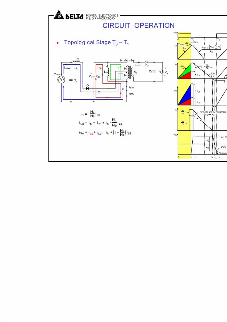
CIRCUIT OPERATION
! Topological Stage T0 – T1LB
N1NP
Vv
N2
NSi LB
T
iLB
iSW
iS
vSW
iMVB
LM
vGS
0
NP
NSi M
T0
in(rec)
NS
LB
i SW
vin(rec)
CF
+i P1
SW
i LB
RL
+
Vo
Cin
D
N1 N2+ = NP
CBVB
+
N2
N1
i Mi in(rec)
DFi CB
LM
i S = 0
i P1 = -N1
NPi LB
i CBiSW = i LB+ i M + i LBN1
NP1=
Ni MiCB = i P1+
NP
i M= - 1 i LB
7/27/2019 90W Single PFC Flyback Adapter
http://slidepdf.com/reader/full/90w-single-pfc-flyback-adapter 12/38
POWER ELECTRONICSR & D LABORATORY
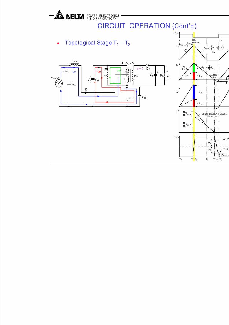
CIRCUIT OPERATION (Cont’d
! Topological Stage T1 – T2
NS
LB
CF
+i P1i LB
RL
+
Vo
Cin
D
N1 N2+ = NP
CBVB
+
N2
N1
i S = 0i M DFi CB
LM
Coss
vin(rec)
i in(rec)
LB
N1NP
Vv
N2
NSi LB
T
iLB
iSW
iS
vSW
iMVB
LM
vGS
0
NP
NSi M
T0
in(rec)
7/27/2019 90W Single PFC Flyback Adapter
http://slidepdf.com/reader/full/90w-single-pfc-flyback-adapter 13/38
POWER ELECTRONICSR & D LABORATORY
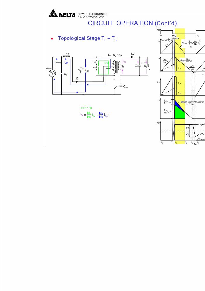
CIRCUIT OPERATION (Cont’
! Topological Stage T2 – T3
NS
LB DF
CF
+i LB
RL
Cin
CBVB
+
N2
N1
iSi M
LM
Coss
io
D
iP1
N1 N2+ = NP
vin(rec)
i in(rec)
NP
NS
i Mi S =
i P1 = i M-
+N2
NS
i LB
LB
N1NP
Vv
N2
NSi LB
iLB
iSW
iS
vSW
iMVB
LM
vGS
0
NP
NSi M
T0
in(rec)
7/27/2019 90W Single PFC Flyback Adapter
http://slidepdf.com/reader/full/90w-single-pfc-flyback-adapter 14/38
POWER ELECTRONICSR & D LABORATORY
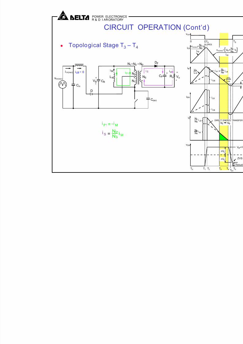
CIRCUIT OPERATION (Cont’d
! Topological Stage T3 – T4
NS
DF
CF
+
RL
+
Vo
Cin
CBVB
+
N2
N1
iSiM
LM
Coss
i o
D
iLB = 0 i P1
N1 N2+ = NP
vin(rec)
i in(rec)
NP
NSi M
i S =
i P1= i M-
LB
N1NPVv
N2
NSi LB
iLB
iSW
iS
vSW
iMVB
LM
vGS
0
NP
NSi M
T0
in(rec)
7/27/2019 90W Single PFC Flyback Adapter
http://slidepdf.com/reader/full/90w-single-pfc-flyback-adapter 15/38
POWER ELECTRONICSR & D LABORATORY
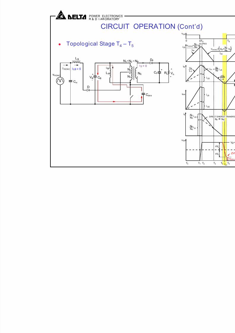
CIRCUIT OPERATION (Cont’
! Topological Stage T4 – T5
NS
LB
CF
+
RL
+
Vo
Cin
CBVB
+
N2
N1
i M
LM
D
Coss
DF
iLB = 0iS = 0
N1 N2+ = NP
vin(rec)
i in(rec)
LB
N1NP
v
N2
NSi LB
iLB
iSW
iS
vSW
iMVB
LM
vGS
0
NP
NSi M
T0
in(rec)
7/27/2019 90W Single PFC Flyback Adapter
http://slidepdf.com/reader/full/90w-single-pfc-flyback-adapter 16/38
POWER ELECTRONICSR & D LABORATORY
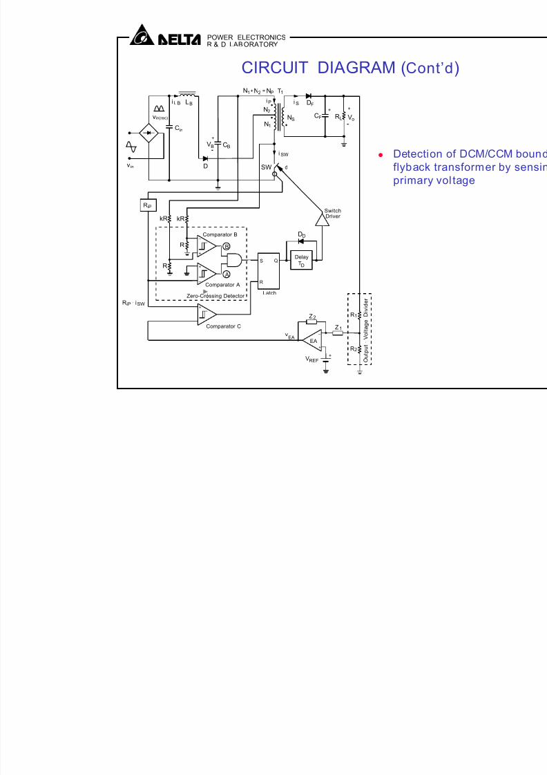
CIRCUIT DIAGRAM (Cont’d)
! Detection of
flyback trans
primary vol ta
RiP
v in
VB
NS
LB
CB
DF
vin(rec) CF
+
iP
SW
i L B
RL
+
Vo
i SW
i S
Cin
iSWRiP.
Z1
Z2
_
+
EA
vEA
d
_
+
D
+
+
N2
N1
kRkR
_
+
_
+
B
A
R
R
R1
R2
O u t p u t - V o l t a g e
D i v i d e r
N1 N2+ = NP
SwitchDriver
R
S Q
Latch
Delay
DT
DD
VREF
T1
Comparator C
Zero-Crossing Detector
Comparator B
Comparator A
7/27/2019 90W Single PFC Flyback Adapter
http://slidepdf.com/reader/full/90w-single-pfc-flyback-adapter 17/38
POWER ELECTRONICSR & D LABORATORY
EXPERIMENTAL CIRCUIT DIAGR
+
3D
1D
4D
2DBL
BD
BC
BYPD
Q
INPUT
FILTER
20N
150µµµµ/400V
75µµµµ
(600V
2N
1N
XF (275µµµµ
PTS30/19
15T
15T90-264
rms V
! Control circuit based on L6565 (ST)
! Detection of DCM/CCM boundary of flyback tra
sensing primary voltage

7/27/2019 90W Single PFC Flyback Adapter
http://slidepdf.com/reader/full/90w-single-pfc-flyback-adapter 18/38
EXECUTIVE SUMMARY
Key characteristics of the 90-W adapter with S2PFC flyback can be summarized as
follows:
1. Worst-case efficiency (low line, full load) ~ 88% - see Table I;
2. Line current harmonics satisfy the standard requirements with a large margin
(>20%) –see Table II;
3. Bulk voltage is always below 400 V:
a) Maximum bulk voltage (at high line and full load) is 396 V – see Fig. 19(a),
b) Bulk voltage at high line and no load is 374 V – see Fig. 19(d);
4. Input power at 240-Vrms line voltage and no load is ~ 700 mW (670-700 mW);
5. Input power at 115-Vrms line voltage and no load is ~ 625 mW (610-640 mW);
6. Switching frequency variations:
a) Switching frequency range at full load is 65-177 kHz,
b) Maximum switching frequency is 228 kHz (at high line and 2.7-A load);
7. Maximum drain-source voltage is 654 V (first turn-off spike at high line) – see Fig.
20.

7/27/2019 90W Single PFC Flyback Adapter
http://slidepdf.com/reader/full/90w-single-pfc-flyback-adapter 19/38
2

7/27/2019 90W Single PFC Flyback Adapter
http://slidepdf.com/reader/full/90w-single-pfc-flyback-adapter 20/38
3
I. CIRCUIT DIAGRAM
A. Power Stage
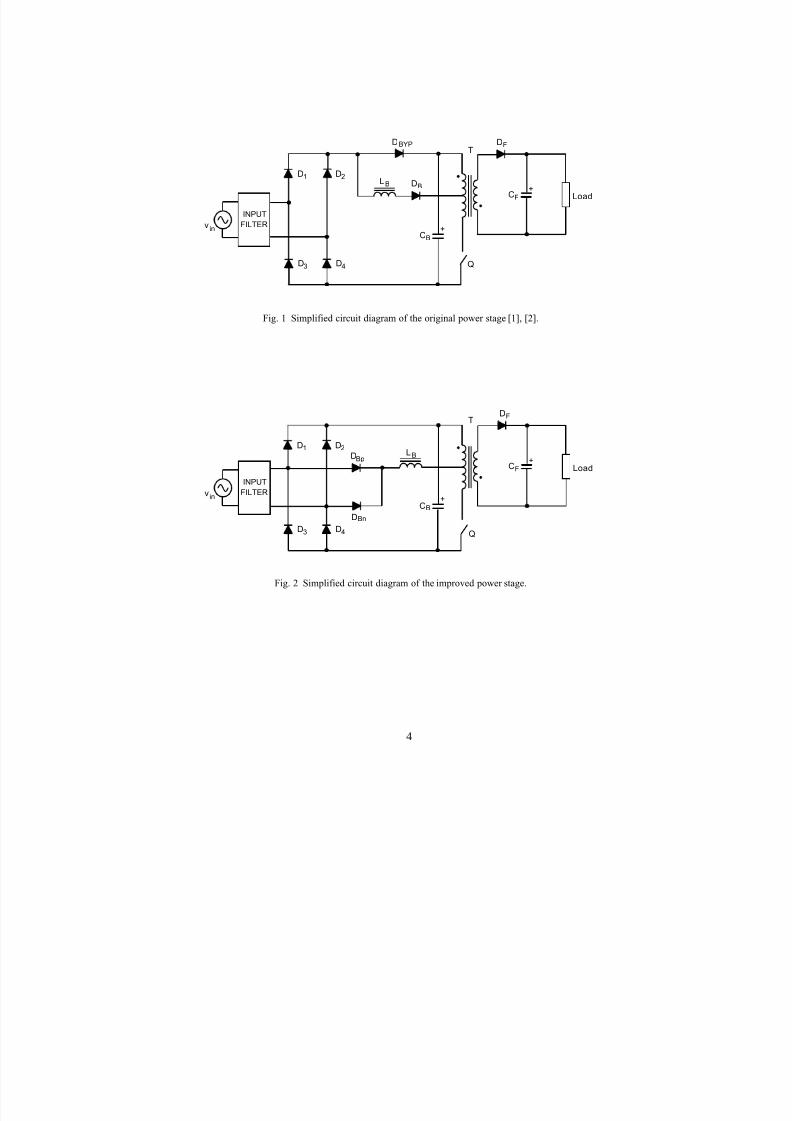
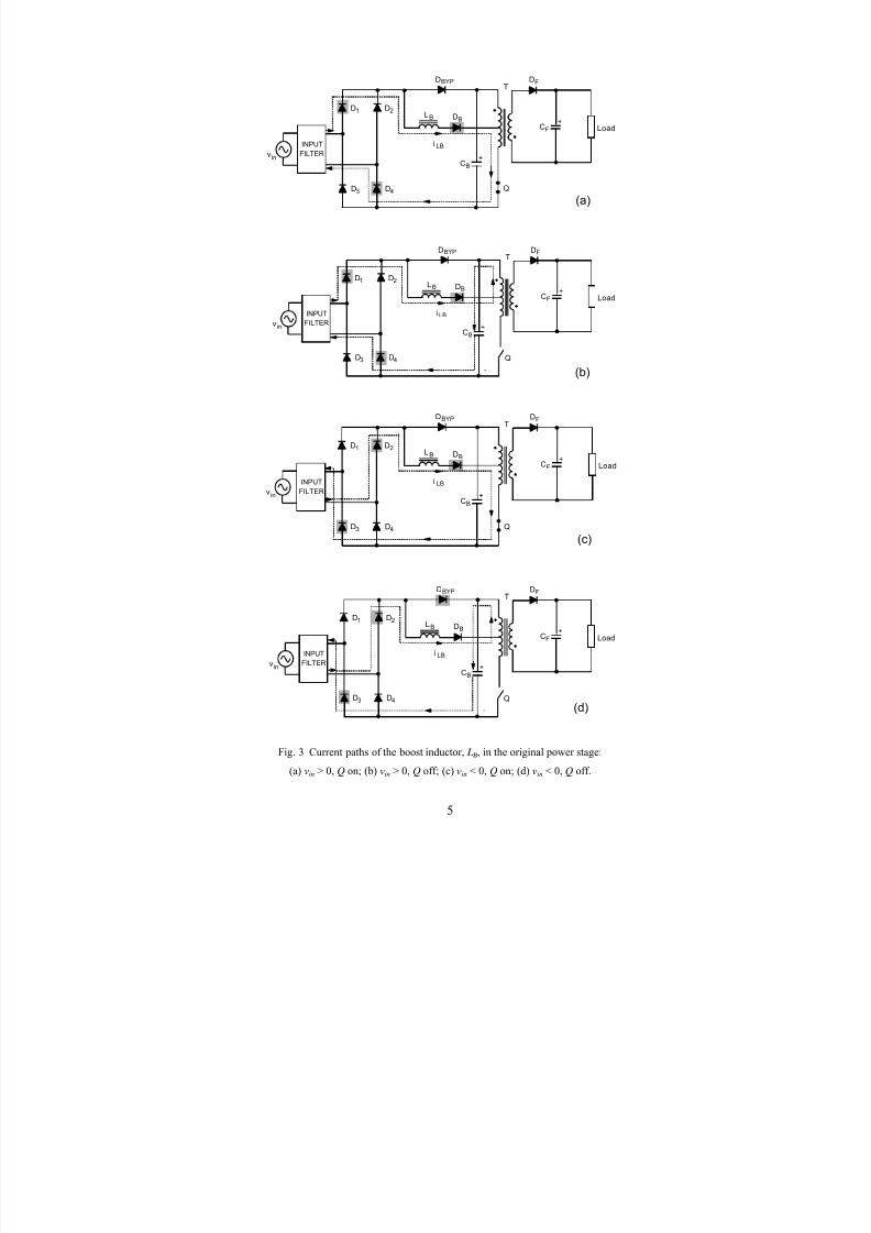
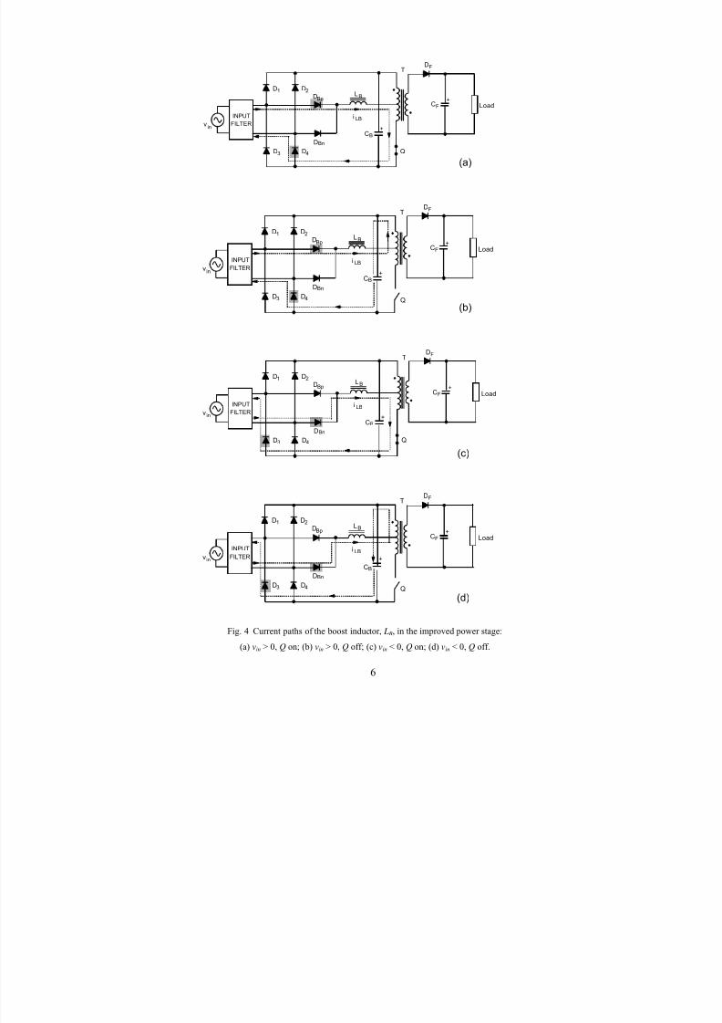
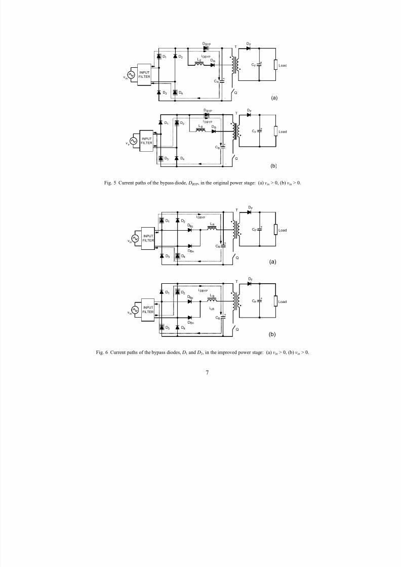
The simplified circuit diagram of the original power stage [1], [2] is shown in Fig. 1. Recently, the
topology of the original power stage was slightly modified, which resulted in an improved efficiency.
The simplified circuit diagram of the improved power stage is shown in Fig. 2. It should be noticed that
the only difference between the power stages in Figs. 1 and 2 is the position of the two diodes outside of
the diode bridge ( D1- D4). However, in the improved power stage in Fig. 2, one diode-forward-voltage
drop is eliminated. Current paths of the boost (PFC) inductor, L B, in the original and improved power
stages are shown in Figs. 3 and 4, respectively. As can be seen in Fig. 3, the current paths of the boost
inductor in Fig. 3 include three diodes, whereas, the current paths of the boost inductor in Fig. 4 include
only two diodes. Similarly, the current paths of the bypass diode, D BYP in Fig. 1, which conducts only
during a short interval around the peaking of the rectified line voltage, also include three diodes, as
shown in Fig. 5. In the improved power stage in Fig. 2, diode D1 serves as the bypass diode during a
positive half cycle of the line voltage, and diode D2 serves as the bypass diode during a negative half cycle of the line voltage. Therefore, the bypass current paths in the power stage in Fig. 2 include only
two diodes, as shown in Fig. 6.
To conclude, the modification of the original power stage in Fig. 1 is achieved as follows:
• Bridge diodes D1 and D2 were eliminated;
• Boost diode D B was replaced with two diodes, D Bp and D Bn (one diode for each half cycle of the
line voltage; therefore, the current stress of diodes D Bp and D Bn is only half of that of diode D B);
and
• Bypass diode D BYP was replaced with two diodes, D1 and D2 (one diode for each half cycle of the
line voltage; therefore, the current stress of diodes D1 and D2 is only half of that of diode D BYP).
7/27/2019 90W Single PFC Flyback Adapter
http://slidepdf.com/reader/full/90w-single-pfc-flyback-adapter 21/38
4
Fig. 1 Simplified circuit diagram of the original power stage [1], [2].
Fig. 2 Simplified circuit diagram of the improved power stage.
+
+
3D
1D
4D
2DBL
BD
BC
BYPD FD
FC
Q
T
inv
INPUT
FILTER
Load
+
+
3D
1D
4D
2D
BpD
BC
FD
FC
Q
T
BnD
inv
INPUT
FILTER
BLLoad
7/27/2019 90W Single PFC Flyback Adapter
http://slidepdf.com/reader/full/90w-single-pfc-flyback-adapter 22/38
5
Fig. 3 Current paths of the boost inductor, L B, in the original power stage:
(a) vin > 0, Q on; (b) vin > 0, Q off; (c) vin < 0, Q on; (d) vin < 0, Q off.
(d)
+
+
3D
1D
4D
2DBL
BD
BC
BYPD FD
FC
Q
T
inv
INPUT
FILTER
Load
LBi
(b)
+
+
3D
1D
4D
2DBL
BD
BC
BYPD FD
FC
Q
T
inv
INPUT
FILTER
Load
LBi
(a)
+
+
3D
1D
4D
2DBL
BD
BC
BYPD FD
FC
Q
T
inv
INPUT
FILTER
Load
LBi
(c)
+
+
3D
1D
4D
2DBL
BD
BC
BYPD FD
FC
Q
T
inv
INPUT
FILTER
Load
LBi
7/27/2019 90W Single PFC Flyback Adapter
http://slidepdf.com/reader/full/90w-single-pfc-flyback-adapter 23/38
6
Fig. 4 Current paths of the boost inductor, L B, in the improved power stage:
(a) vin > 0, Q on; (b) vin > 0, Q off; (c) vin < 0, Q on; (d) vin < 0, Q off.
+
+
3D
1D
4D
2D
BpD
BC
FD
FC
Q
T
BnD
inv
INPUT
FILTER
BL
Load
LBi
(b)
+
+
3D
1D
4D
2D
BpD
BC
FD
FC
Q
T
BnD
inv
INPUT
FILTER
BL
Load
LBi
(d)
(a)
+
+
3D
1D
4D
2D
BpD
BC
FD
FC
T
BnD
inv
INPUT
FILTER
BL
Load
LBi
Q
(c)
+
+
3D
1D
4D
2D
BpD
BC
FD
FC
T
BnD
inv
INPUT
FILTER
BL
Load
LBi
Q
7/27/2019 90W Single PFC Flyback Adapter
http://slidepdf.com/reader/full/90w-single-pfc-flyback-adapter 24/38
7
Fig. 5 Current paths of the bypass diode, D BYP, in the original power stage: (a) vin > 0, (b) vin > 0.
Fig. 6 Current paths of the bypass diodes, D1 and D2, in the improved power stage: (a) vin > 0, (b) vin > 0.
(b)
+
+
3D
1D
4D
2DBL
BD
BC
BYPD FD
FC
Q
T
inv
INPUT
FILTER
Load
DBYPi
(a)
+
+
3D
1D
4D
2DBL
BD
BC
BYPD FD
FC
Q
T
inv
INPUT
FILTER
Load
DBYPi
(a)
+
+
3D
1D
4D
2D
BpD
BC
FD
FC
Q
T
BnD
inv
INPUT
FILTER
BL
Load
DBYPi
(b)
Load
+
+
3D
1D
4D
2D
BpD
BC
FD
FC
Q
T
BnD
inv
INPUT
FILTER
BL
LBi
DBYPi
7/27/2019 90W Single PFC Flyback Adapter
http://slidepdf.com/reader/full/90w-single-pfc-flyback-adapter 25/38
8
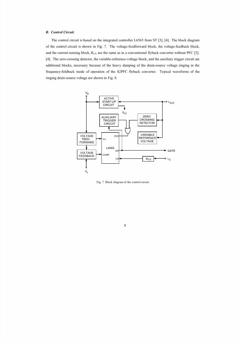
B. Control Circuit
The control circuit is based on the integrated controller L6565 from ST [3], [4]. The block diagram
of the control circuit is shown in Fig. 7. The voltage-feedforward block, the voltage-feedback block,
and the current-sensing block, RCS , are the same as in a conventional flyback converter without PFC [3],
[4]. The zero-crossing detector, the variable-reference-voltage block, and the auxiliary trigger circuit are
additional blocks, necessary because of the heavy damping of the drain-source voltage ringing in the
frequency-foldback mode of operation of the S2PFC flyback converter. Typical waveforms of the
ringing drain-source voltage are shown in Fig. 8.
Fig. 7 Block diagram of the control circuit.
ACTIVESTART-UPCIRCUIT
AUXILIARYTRIGGERCIRCUIT
VOLTAGE
FEED-FORWARD
VOLTAGEFEEDBACK
ZEROCROSSINGDETECTOR
CCV
VARIABLE
REFERENCEVOLTAGE
AUXv
CSR
FF
COMP
V
ZCD
GD
CS
GATE
QI
Vo
L6565
BV
7/27/2019 90W Single PFC Flyback Adapter
http://slidepdf.com/reader/full/90w-single-pfc-flyback-adapter 26/38
9
(a) (b)
(c) (d)
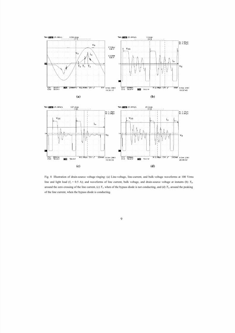
Fig. 8 Illustration of drain-source voltage ringing: (a) Line-voltage, line-current, and bulk voltage waveforms at 100 Vrms
line and light load ( I o = 0.5 A); and waveforms of line current, bulk voltage, and drain-source voltage at instants (b) T 0,
around the zero crossing of the line current, (c) T 1, when of the bypass diode is not conducting, and (d) T 2, around the peaking
of the line current, when the bypass diode is conducting.
vB
v in i in
vDS
i in
T1 T2T0 vB
vDS
i in
vDS i in
vB vB
7/27/2019 90W Single PFC Flyback Adapter
http://slidepdf.com/reader/full/90w-single-pfc-flyback-adapter 27/38
10
The additional zero-crossing detector is necessary because the internal zero-crossing detector of the
L6565 controller chip has a hysteresis equal to 0.5 V, which is too large to detect the zero crossings
when the amplitude of the ringing drain-source voltage becomes too small (because of the heavy
damping). The external zero-crossing detector is implemented with the integrated comparator LM393,
which has a very small hysteresis (±5mV). The circuit diagram of the external zero-crossing detector is
shown in Fig. 9. It should be noticed in Fig. 9, that the reference voltage of the comparator (at pin 2 of
LM393) is constant, slightly larger than zero.
Fig. 9 Circuit diagram of the zero-current detector.
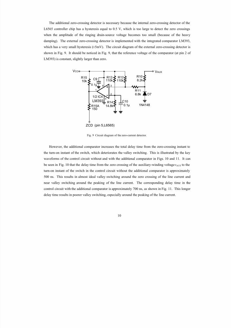
However, the additional comparator increases the total delay time from the zero-crossing instant to
the turn-on instant of the switch, which deteriorates the valley switching. This is illustrated by the key
waveforms of the control circuit without and with the additional comparator in Figs. 10 and 11. It can
be seen in Fig. 10 that the delay time from the zero crossing of the auxiliary-winding voltage v AUX to the
turn-on instant of the switch in the control circuit without the additional comparator is approximately
500 ns. This results in almost ideal valley switching around the zero crossing of the line current and near valley switching around the peaking of the line current. The corresponding delay time in the
control circuit with the additional comparator is approximately 700 ns, as shown in Fig. 11. This longer
delay time results in poorer valley switching, especially around the peaking of the line current.
R108.2k
R116.8k
1N4148
D7
C100.1µ
0.1µ
R13110k
R12110k
R1414.8k
C9
1/2 IC4
LM393
8
2
3
4
1
R1510k
VCC V AUX
R15A150
ZCD (pin 5,L6565)
7/27/2019 90W Single PFC Flyback Adapter
http://slidepdf.com/reader/full/90w-single-pfc-flyback-adapter 28/38
11
(a) (b)
Fig. 10 Key waveforms of the control circuit without additional zero-crossing comparator: auxiliary-winding voltage v AUX ,
ZCD-pin voltage v ZCD, and gate-drive voltage vGD (a) around the zero crossing of the line current and (b) around the peaking
of the line current, at 100-Vrms line voltage and full load (20 V/4.5 A).
(a) (b)
Fig. 11 Key waveforms of the control circuit with additional zero-crossing comparator: auxiliary-winding voltage v AUX ,
ZCD-pin voltage v ZCD, and gate-drive voltage vGD (a) around the zero crossing of the line current and (b) around the peaking
of the line current, at 100-Vrms line voltage and full load (20 V/4.5 A).
vAUX
vZCD
vGD
iin=0
vAUX
vZCD vGD
iin
vAUX
vZCD
vGD
iin=0
vAUX
vZCD vGD
iin
7/27/2019 90W Single PFC Flyback Adapter
http://slidepdf.com/reader/full/90w-single-pfc-flyback-adapter 29/38
12
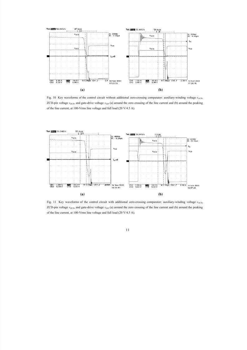
The delay time of the additional comparator is compensated by moving the instant of the “zero-
crossing” detection before the actual zero crossing instant of the auxiliary-winding voltage v AUX . This is
achieved by a variable reference voltage for the comparator. The implementation of the variable
reference voltage is shown in Fig. 12. Key waveforms of the control circuit are shown in Fig. 13. As
can be seen in Fig. 13, during the off time of the switch, the reference voltage is exponentially increased
to approximately 75% of the auxiliary-winding voltage level. Therefore, the “zero-crossing” detection
is achieved right after the drain-source voltage starts to decrease, i.e. before the actual zero-crossing
instant. The delay time from the instant auxiliary-winding voltage v AUX crosses reference voltage v REF to
the turn-on instant of the switch is again approximately 700 ns as in Fig. 11. However, as the same
delay time starts earlier, the variable reference voltage results in a significantly better valley switching
compared to that in Fig. 11.
Fig. 12 Circuit diagram of the zero-current detector with variable reference voltage.
R108.2k
R116.8k
1N4148
D7
0.1µ
R13110k
R12110k
R1414k
C9
1/2 IC4
LM393
8
2
3
4
1
Q6Q5
R14A220k
R2515k
R26
1.5k
D9
1N4148
2N2222
2N2222
R2710k
VCC V AUX
R15A
150
ZCD
(pin 5,L6565)
7/27/2019 90W Single PFC Flyback Adapter
http://slidepdf.com/reader/full/90w-single-pfc-flyback-adapter 30/38
13
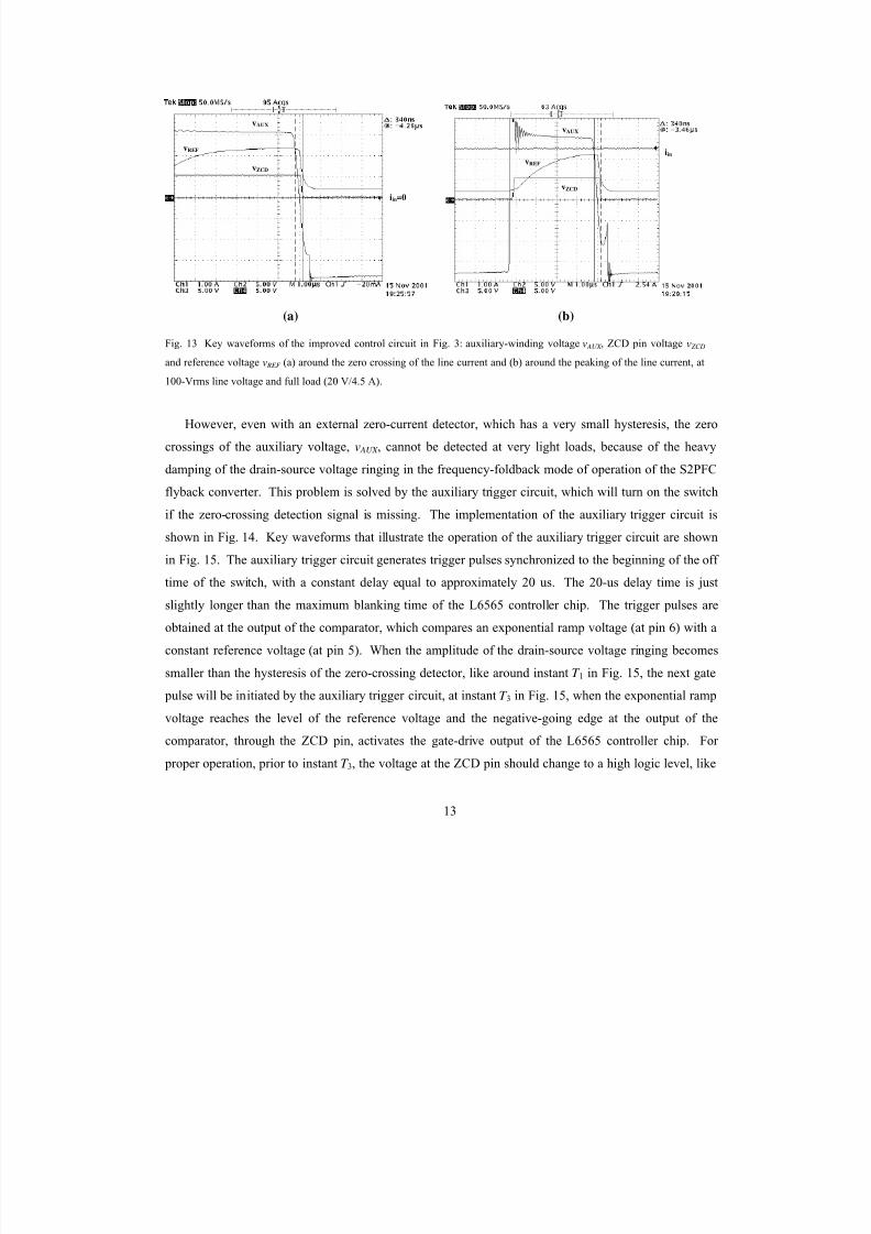
(a) (b)
Fig. 13 Key waveforms of the improved control circuit in Fig. 3: auxiliary-winding voltage v AUX , ZCD pin voltage v ZCD
and reference voltage v REF (a) around the zero crossing of the line current and (b) around the peaking of the line current, at
100-Vrms line voltage and full load (20 V/4.5 A).
However, even with an external zero-current detector, which has a very small hysteresis, the zero
crossings of the auxiliary voltage, v AUX , cannot be detected at very light loads, because of the heavy
damping of the drain-source voltage ringing in the frequency-foldback mode of operation of the S2PFC
flyback converter. This problem is solved by the auxiliary trigger circuit, which will turn on the switch
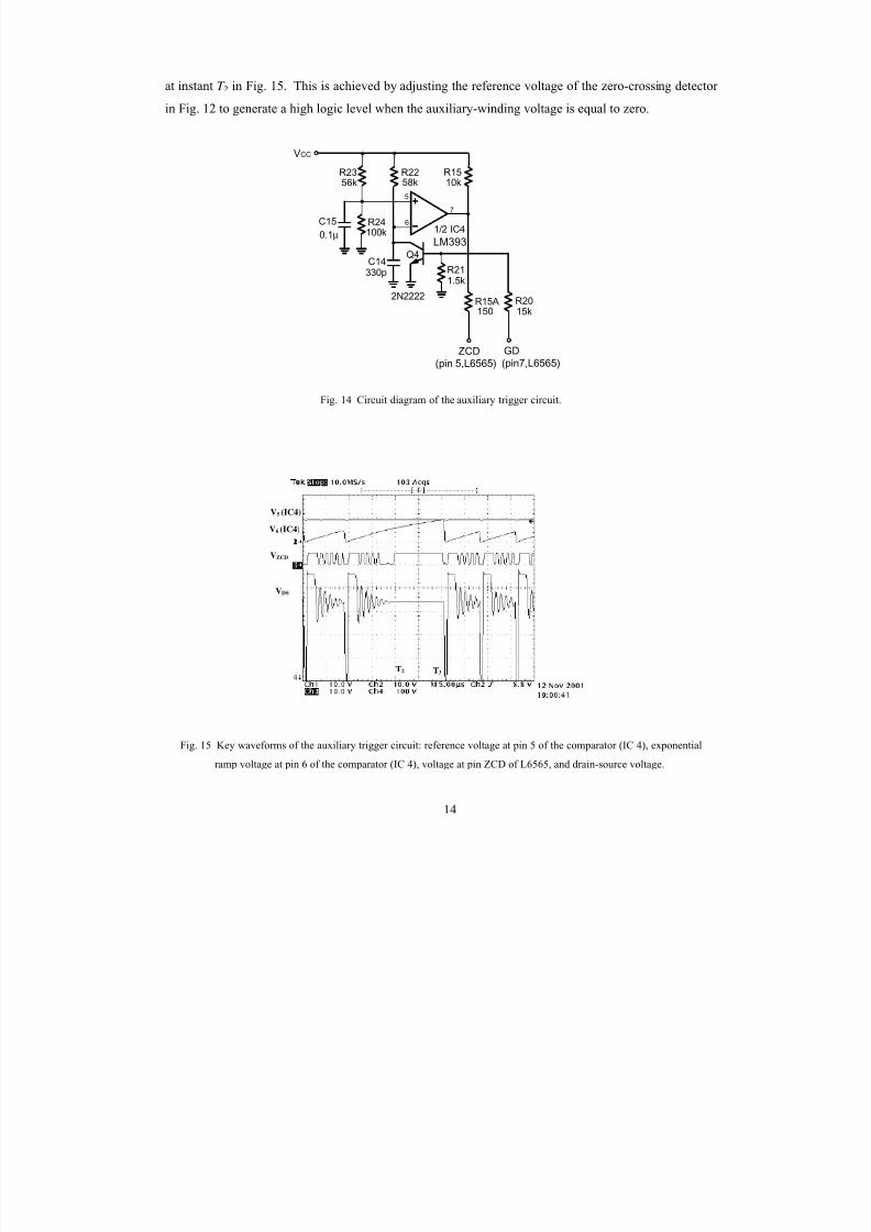
if the zero-crossing detection signal is missing. The implementation of the auxiliary trigger circuit is
shown in Fig. 14. Key waveforms that illustrate the operation of the auxiliary trigger circuit are shown
in Fig. 15. The auxiliary trigger circuit generates trigger pulses synchronized to the beginning of the off
time of the switch, with a constant delay equal to approximately 20 us. The 20-us delay time is just
slightly longer than the maximum blanking time of the L6565 controller chip. The trigger pulses are
obtained at the output of the comparator, which compares an exponential ramp voltage (at pin 6) with a
constant reference voltage (at pin 5). When the amplitude of the drain-source voltage ringing becomes
smaller than the hysteresis of the zero-crossing detector, like around instant T 1 in Fig. 15, the next gate
pulse will be initiated by the auxiliary trigger circuit, at instant T 3 in Fig. 15, when the exponential ramp
voltage reaches the level of the reference voltage and the negative-going edge at the output of the
comparator, through the ZCD pin, activates the gate-drive output of the L6565 controller chip. For
proper operation, prior to instant T 3, the voltage at the ZCD pin should change to a high logic level, like
vAUX
vZCD
vREF
iin=0
vAUX
vZCD
vREF
iin
7/27/2019 90W Single PFC Flyback Adapter
http://slidepdf.com/reader/full/90w-single-pfc-flyback-adapter 31/38
14
at instant T 2 in Fig. 15. This is achieved by adjusting the reference voltage of the zero-crossing detector
in Fig. 12 to generate a high logic level when the auxiliary-winding voltage is equal to zero.
Fig. 14 Circuit diagram of the auxiliary trigger circuit.
Fig. 15 Key waveforms of the auxiliary trigger circuit: reference voltage at pin 5 of the comparator (IC 4), exponential
ramp voltage at pin 6 of the comparator (IC 4), voltage at pin ZCD of L6565, and drain-source voltage.
R1510k
7
6
R2258k
330p
C15 R24100k
5
0.1µ
C14R21
R2356k
1.5k
Q4
1/2 IC4
LM393
2N2222
VCC
R15A R2015k150
ZCD GD
(pin 5,L6565) (pin7,L6565)
T3T2
VZCD
VDS
V5 (IC4)
V6 (IC4)
7/27/2019 90W Single PFC Flyback Adapter
http://slidepdf.com/reader/full/90w-single-pfc-flyback-adapter 32/38
15
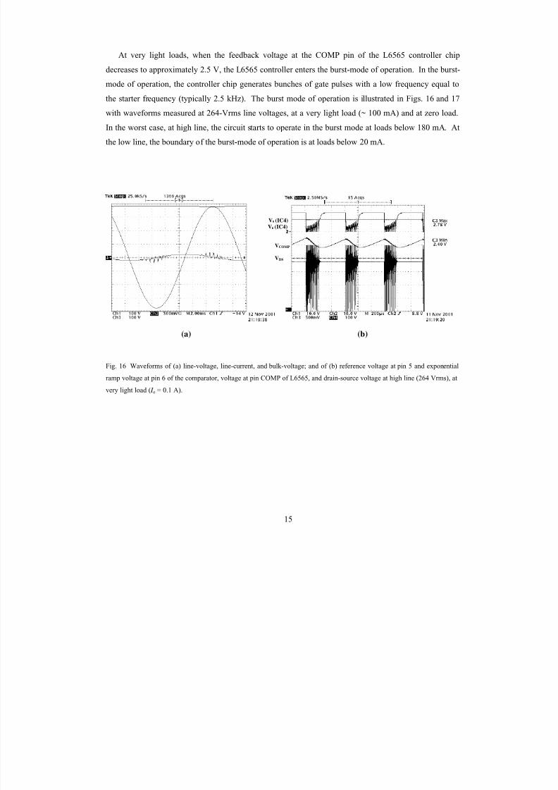
At very light loads, when the feedback voltage at the COMP pin of the L6565 controller chip
decreases to approximately 2.5 V, the L6565 controller enters the burst-mode of operation. In the burst-
mode of operation, the controller chip generates bunches of gate pulses with a low frequency equal to
the starter frequency (typically 2.5 kHz). The burst mode of operation is illustrated in Figs. 16 and 17
with waveforms measured at 264-Vrms line voltages, at a very light load (~ 100 mA) and at zero load.
In the worst case, at high line, the circuit starts to operate in the burst mode at loads below 180 mA. At
the low line, the boundary of the burst-mode of operation is at loads below 20 mA.
(a) (b)
Fig. 16 Waveforms of (a) line-voltage, line-current, and bulk-voltage; and of (b) reference voltage at pin 5 and exponential
ramp voltage at pin 6 of the comparator, voltage at pin COMP of L6565, and drain-source voltage at high line (264 Vrms), at
very light load ( I o = 0.1 A).
VCOMP
VDS
V5 (IC4)V6 (IC4)

7/27/2019 90W Single PFC Flyback Adapter
http://slidepdf.com/reader/full/90w-single-pfc-flyback-adapter 33/38
16
(a) (b)
Fig. 17 Waveforms of (a) line-voltage, line-current, and bulk-voltage; and of (b) reference voltage at pin 5 and exponential
ramp voltage at pin 6 of the comparator, voltage at pin COMP of L6565, and drain-source voltage at high line (264 Vrms), at
zero load.
C. Complete Circuit Diagram
The complete circuit diagram is shown on a separate page.
VDS
V5 (IC4)
V6 (IC4)
VCOMP
7/27/2019 90W Single PFC Flyback Adapter
http://slidepdf.com/reader/full/90w-single-pfc-flyback-adapter 34/38
17
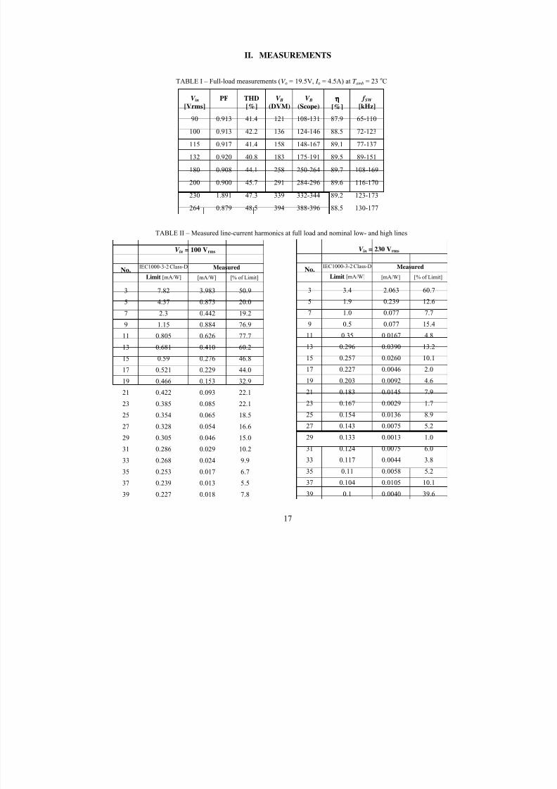
II. MEASUREMENTS
TABLE I – Full-load measurements (V o = 19.5V, I o = 4.5A) at T amb = 23 oC
V in
[Vrms]
PF THD
[%]
V B
(DVM)
V B
(Scope)
ηηηη
[%]
f SW
[kHz]
90 0.913 41.4 121 108-131 87.9 65-110
100 0.913 42.2 136 124-146 88.5 72-123
115 0.917 41.4 158 148-167 89.1 77-137
132 0.920 40.8 183 175-191 89.5 89-151
180 0.908 44.1 258 250-264 89.7 108-169
200 0.900 45.7 291 284-296 89.6 116-170
230 1.891 47.3 339 332-344 89.2 123-173
264 0.879 48.5 394 388-396 88.5 130-177
TABLE II – Measured line-current harmonics at full load and nominal low- and high lines
V in = 100 Vrms
No.IEC1000-3-2 Class-D
Limit [mA/W]
Measured
[mA/W] [% of Limit]
3 7.82 3.983 50.9
5 4.37 0.873 20.0
7 2.3 0.442 19.2
9 1.15 0.884 76.9
11 0.805 0.626 77.7
13 0.681 0.410 60.2
15 0.59 0.276 46.8
17 0.521 0.229 44.0
19 0.466 0.153 32.9
21 0.422 0.093 22.1
23 0.385 0.085 22.1
25 0.354 0.065 18.5
27 0.328 0.054 16.6
29 0.305 0.046 15.0
31 0.286 0.029 10.2
33 0.268 0.024 9.9
35 0.253 0.017 6.7
37 0.239 0.013 5.5
39 0.227 0.018 7.8
V in = 230 Vrms
No.IEC1000-3-2 Class-D
Limit [mA/W]
Measured
[mA/W] [% of Limit]
3 3.4 2.063 60.7
5 1.9 0.239 12.6
7 1.0 0.077 7.7
9 0.5 0.077 15.4
11 0.35 0.0167 4.8
13 0.296 0.0390 13.2
15 0.257 0.0260 10.1
17 0.227 0.0046 2.0
19 0.203 0.0092 4.6
21 0.183 0.0145 7.9
23 0.167 0.0029 1.7
25 0.154 0.0136 8.9
27 0.143 0.0075 5.229 0.133 0.0013 1.0
31 0.124 0.0075 6.0
33 0.117 0.0044 3.8
35 0.11 0.0058 5.2
37 0.104 0.0105 10.1
39 0.1 0.0040 39.6
7/27/2019 90W Single PFC Flyback Adapter
http://slidepdf.com/reader/full/90w-single-pfc-flyback-adapter 35/38
18
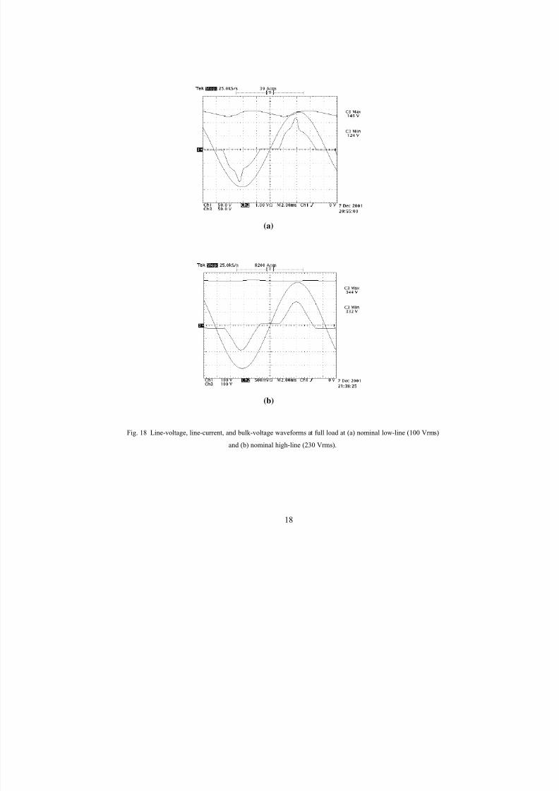
(a)
(b)
Fig. 18 Line-voltage, line-current, and bulk-voltage waveforms at full load at (a) nominal low-line (100 Vrms)
and (b) nominal high-line (230 Vrms).
7/27/2019 90W Single PFC Flyback Adapter
http://slidepdf.com/reader/full/90w-single-pfc-flyback-adapter 36/38
19
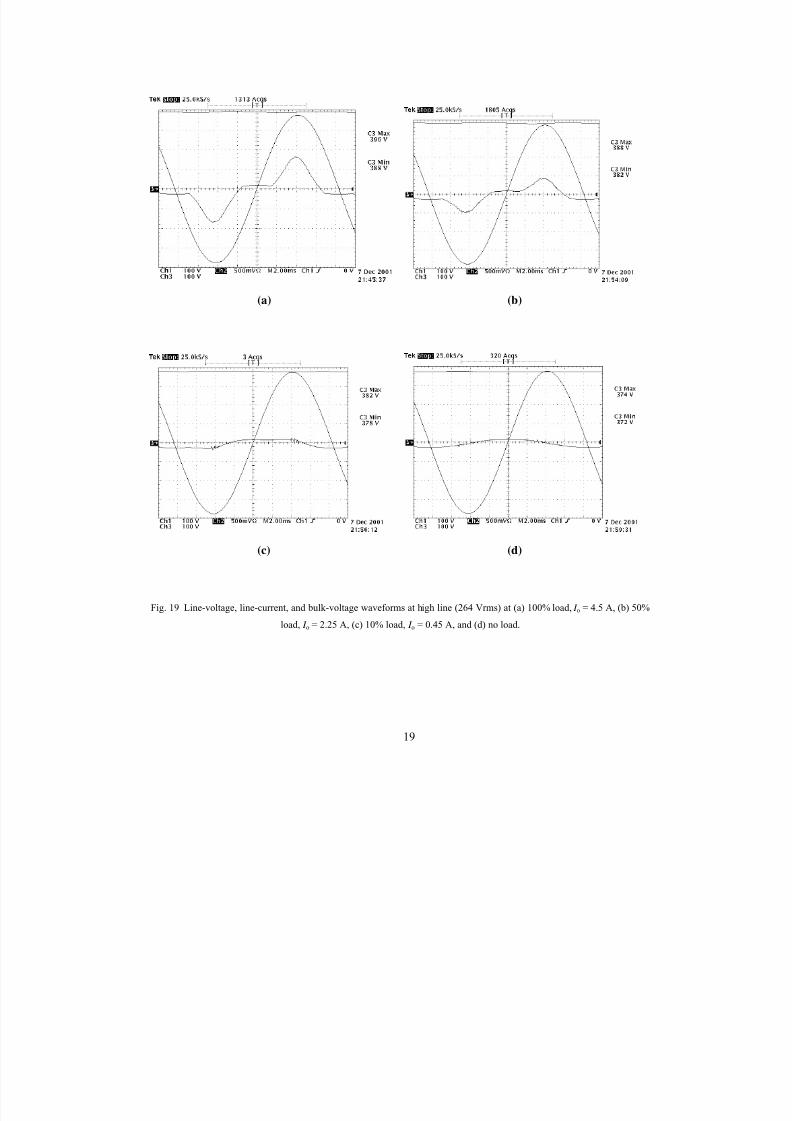
(a) (b)
(c) (d)
Fig. 19 Line-voltage, line-current, and bulk-voltage waveforms at high line (264 Vrms) at (a) 100% load, I o = 4.5 A, (b) 50%
load, I o = 2.25 A, (c) 10% load, I o = 0.45 A, and (d) no load.
7/27/2019 90W Single PFC Flyback Adapter
http://slidepdf.com/reader/full/90w-single-pfc-flyback-adapter 37/38
20
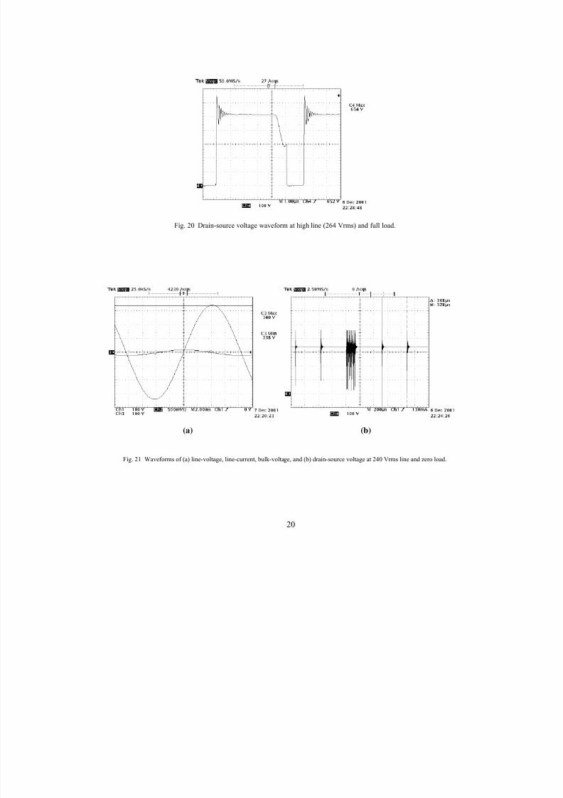
Fig. 20 Drain-source voltage waveform at high line (264 Vrms) and full load.
(a) (b)
Fig. 21 Waveforms of (a) line-voltage, line-current, bulk-voltage, and (b) drain-source voltage at 240 Vrms line and zero load.

7/27/2019 90W Single PFC Flyback Adapter
http://slidepdf.com/reader/full/90w-single-pfc-flyback-adapter 38/38
III. SUMMARY
Key characteristics of the 90-W adapter with S2PFC flyback can be summarized as follows:
8. Worst-case efficiency (low line, full load) ~ 88% - see Table I;
9. Line current harmonics satisfy the standard requirements with a large margin (>20%) –see Table II;
10. Bulk voltage is always below 400 V:
a) Maximum bulk voltage (at high line and full load) is 396 V – see Fig. 19(a),
b) Bulk voltage at high line and no load is 374 V – see Fig. 19(d);
11. Input power at 240-Vrms line voltage and no load is ~ 700 mW (670-700 mW);
12. Input power at 115-Vrms line voltage and no load is ~ 625 mW (610-640 mW);
13. Switching frequency variations:
a) Switching frequency range at full load is 65-177 kHz,
b) Maximum switching frequency is 228 kHz (at high line and 2.7-A load);
14. Maximum drain-source voltage is 654 V (first turn-off spike at high line) – see Fig. 20.
IV. REFERENCES
[1] M.M. Jovanovi and L. Huber, “Ac/dc flyback converter with improved power factor and reduced
switching loss,” U.S. Patent No. 5991172, Nov. 1999.
[2] L. Huber and M.M. Jovanovi , “Single-stage, single-switch input-current-shaping technique with
reduced switching loss,” IEEE Applied Power Electronics Conference (APEC) Proc., pp. 98-104,
Mar. 1999.
[3] - , “L6565 quasi-resonant controller,” ST Microelectronics, Jan. 2001.
[4] C. Adragna, “Design of offline quasi-resonant flyback converters with L6565,” AN1326, ST
Microelectronics, Jan. 2001.