using modules in allegro pcb editor -...
TRANSCRIPT
Using Modules in Allegro PCB Editor Design Reuse for Performance 1
Using Modules in Allegro PCB Editor
Design Reuse for Performance
Presented at CDNLive! Silicon Valley
Session 5.8 – September 13, 2006
George Patrick Tektronix, Inc.
P.O. Box 500, M/S 39-512 Beaverton, OR 97077-0001
George Patrick CDNLive! Silicon Valley 2006 September 13, 2006

Using Modules in Allegro PCB Editor Design Reuse for Performance 2
INTRODUCTION Tektronix is a world-class Test and Measurement equipment OEM, designing and manufacturing high bandwidth oscilloscopes, logic analyzers, spectrum analyzers, real-time and stored video quality analysis equipment, and network monitoring and test equipment. Many of these products are designed to measure multiple channels simultaneously; and as edge rates and analog bandwidths have expanded, so has the difficulty in making sure that those channels are identical so the user knows that a timing problem is in their design, not in their ‘scope. One of the ways we solve this problem is with design reuse modules.
This paper covers only the physical layout elements of design reuse, for more information on the Allegro Design Editor HDL side of things refer to the paper written by my colleague, Harry Bartley, presented at Session 6.9 of the conference.
WHAT IS A MODULE? Here is Cadence’s explanation of modules from their user documentation:
“In Allegro PCB Editor, modules are collections of physical entities that can include other modules. Modules may or may not have logic (represented by nets, components, and so on.) or a block (a collection of schematic information a schematic tool uses) associated with them. They can be permanently stored as module definition databases (modulename.mdd) in library files using the module path (modulepath) environment variable.”
This doesn’t really explain what modules are used for or why someone might want to use them, so a revised and expanded explanation is in order:
“A design reuse module is a collection of elements grouped together and saved externally so they can be used as an individual unit one or more times inside one or more Allegro PCB Editor designs. These elements can include other modules, symbol packages, lines, shapes, text, and logic that enable their easy reuse in the same or different designs without additional manipulation by the circuit or layout designers.”
The process that was previously used to perform this function was more involved and error prone than the procedure outlined here. At Tektronix, sectional numbering is commonly used on large boards so that the functional area a part is used in can be seen more easily. A clock generator circuit might be numbered in between 100 and 199; a data acquisition section might be between 200 and 299, and so forth. Once a section that the circuit designer wanted replicated was completely finished a sub-drawing of the objects to be replicated was extracted. The resultant file was manually edited to transition the reference designators into the required range (or run through a script to do the same thing), and then imported back into Allegro placed in the new location. Sometimes it even worked that easily. Usually there would be a slight discrepancy in the way the circuit was packaged by the circuit designer and the whole thing would fall apart, requiring the layout designer to swap parts and manually reroute, or manually editing the sub-drawing file until it was correct. This process was repeated until all the sections were placed. When other circuits were placed and routed the individual sections would often end up with differences between each other that could cause differences in the circuit
George Patrick CDNLive! Silicon Valley 2006 September 13, 2006

Using Modules in Allegro PCB Editor Design Reuse for Performance 3
performance. The procedure outlined below is much easier, more accurate, and ultimately less error-prone than these methods, and will ensure that all sections are identical if followed.
TRADEOFFS Design reuse and modules have benefits and drawbacks, just like any design process. Some advantages are:
Figure 1
DESIGN TIME Internal Design Reuse increases the speed of releasing boards, since 80% or more of the layout work in the typical multi-channel test instrument is placement and routing of the individual channels. There are trade-offs involved in this process that will be discussed later that makes the speed increases less than might be assumed by some at first. But if the time to lay out a board without modules is compared to the time it takes to lay out a board with modules there will be a considerable savings.
STANDARDIZATION The availability of general-use modules can act as a standardizing influence within a company, as long as they are documented and advertised to a wide enough audience. When standard modules such as power converters, clock generators, or display circuits are used in multiple designs across multiple products, even more time savings can be realized.
George Patrick CDNLive! Silicon Valley 2006 September 13, 2006

Using Modules in Allegro PCB Editor Design Reuse for Performance 4
PERFORMANCE Design reuse allows replication of not only circuit design into multiple channels, but replication of the exact layout elements as well. Since customers can be assured that a signal processed by one channel will be traveling through exactly the same layout elements as another channel (within manufacturing and part value tolerances, of course), they can be more certain that a signal processed by one channel will more closely resemble one processed by another channel than might have been the case in the past. This increases the performance of the end product significantly.
Disadvantages include:
CHANGES Changes to a modular design, especially one using hierarchical modules, can be painful and appear slow to those not accustomed to the process. The change process can become so time consuming that the layout effectively grinds to a halt waiting for multiple changes to filter up through the modules if changes are not strictly controlled.
EXPECTATIONS Many design engineers think that the layout should be able to be completed in much less time than is actually the case. They see that 80% of the board is being divided into 4 identical modules, see that a similar board took 400 hours to complete without modules, and estimate their design should be complete in 160 hours (40% of the time it took to complete the other board.) When the board is done in 280 hours (because of the changes), they are upset that the board is late even though they still saved 30% of the time it would have taken with a conventional layout. The time savings are NOT a direct function, and the design engineers and project managers need to be told this before they begin calculating availability dates or they are going to be disappointed.
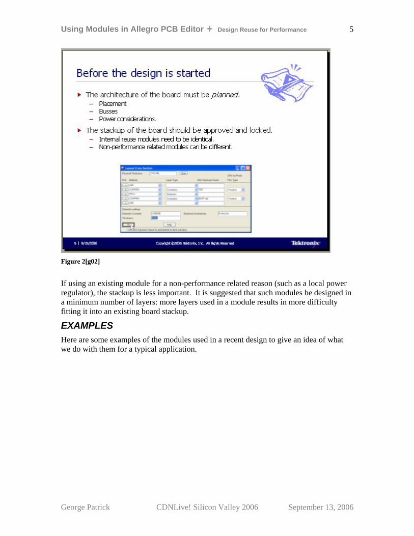
PRELIMINARIES When starting a design that is intended to use internal design reuse, some advance planning must me done. This is the same thing that should be done for any board, but it is critical to the success of a board that uses hierarchical modules for performance reasons. The general parts layout should be considered in advance and the implications when the parts are placed inside the modules planned. Busses should be planned in a similar fashion, the routing in a module should not be moved once it is placed, and some time spent in extra advance planning at this point may save many hours of pain later. General power considerations such as decoupling and plane layout should be planned at this point as well.
Locking down the stackup early is a requirement for a performance driven design reuse board. Although Allegro now allows importing modules that have a different stackup than the root board, it is really not a good idea in this application. Much of the signal and power simulation can be done in smaller “chunks” when using modules, and to do this properly the same stackup must be used in each module. The impedance and power requirements of the bare board should also be considered now, since some of the techniques outlined later require exchange of technology files.
George Patrick CDNLive! Silicon Valley 2006 September 13, 2006
Using Modules in Allegro PCB Editor Design Reuse for Performance 5
Figure 2[g02]
If using an existing module for a non-performance related reason (such as a local power regulator), the stackup is less important. It is suggested that such modules be designed in a minimum number of layers: more layers used in a module results in more difficulty fitting it into an existing board stackup.
EXAMPLES Here are some examples of the modules used in a recent design to give an idea of what we do with them for a typical application.
George Patrick CDNLive! Silicon Valley 2006 September 13, 2006

Using Modules in Allegro PCB Editor Design Reuse for Performance 6
Figure 3
Figure 3 shows the demux_acqmem module. It consists of a custom ASIC, two memory modules, and associated decoupling and termination parts. It is the most common module on the board, used a total of 32 times. It was the first module completed, and was placed in simulation and fine-tuned (including use of the Power Integrity tool), before any other modules were finalized.
This is also an example how planning is always a victim of vendors. During the ASIC design and packaging phases we worked closely with the IC and packaging designers to make sure the memories would be able to flow cleanly into the BGA so that a minimal amount of matching would be done. After our ASIC tape-out, the vendor decided that there wasn’t going to be enough of a market and changed their minds about manufacturing the memories. A new memory part was selected but, naturally, the new ones weren’t a “pin-for-pin” replacement for the old. And we were now using the ASIC with another product which was almost ready to go to production using a different memory part. So this PCB design had to change, thus all the ugly serpentine matching.
Figure 4
Figure 4 shows the digitizer_pipe module. It is the first “hierarchical module,” and is created by placing two demux_acqmem modules inside the “digitizer” design (.brd) file, creating a module file from the whole thing. By the way, once the digitizer_pipe module file is created, the two digitizer_pipe modules lose their identity as modules and are treated like any other parts inside the new module.
George Patrick CDNLive! Silicon Valley 2006 September 13, 2006
Using Modules in Allegro PCB Editor Design Reuse for Performance 7
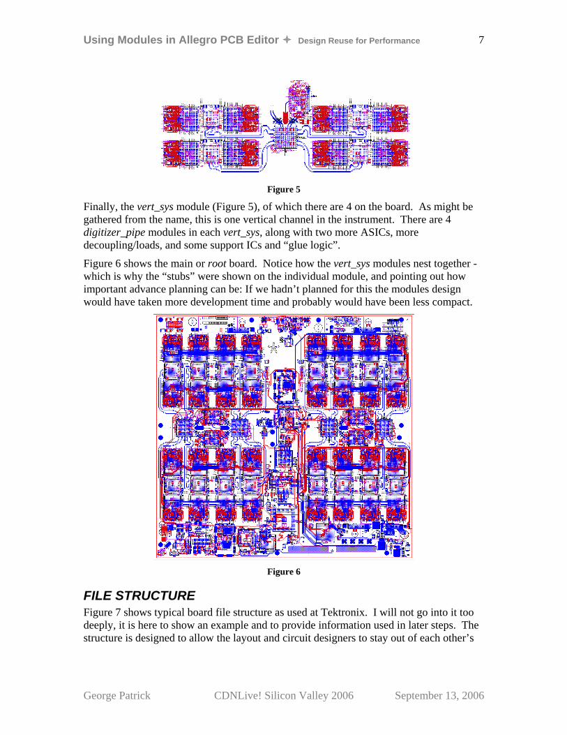
Figure 5
Finally, the vert_sys module (Figure 5), of which there are 4 on the board. As might be gathered from the name, this is one vertical channel in the instrument. There are 4 digitizer_pipe modules in each vert_sys, along with two more ASICs, more decoupling/loads, and some support ICs and “glue logic”.
Figure 6 shows the main or root board. Notice how the vert_sys modules nest together - which is why the “stubs” were shown on the individual module, and pointing out how important advance planning can be: If we hadn’t planned for this the modules design would have taken more development time and probably would have been less compact.
Figure 6
FILE STRUCTURE Figure 7 shows typical board file structure as used at Tektronix. I will not go into it too deeply, it is here to show an example and to provide information used in later steps. The structure is designed to allow the layout and circuit designers to stay out of each other’s
George Patrick CDNLive! Silicon Valley 2006 September 13, 2006

Using Modules in Allegro PCB Editor Design Reuse for Performance 8
way and allow easier archiving of the layout. It is not compatible with the “stock” Cadence directory structure.
The “board” directory contains all the files associated with the physical layout of the board. Inside the board directory is a single directory for all the module (.mdd) files (named modules in this paper), and a separate directory for each module’s database (.brd) file (named identically to the schematic name for the module). This is done to allow the automation to find files that need special handling by the archive system.
The design engineer decides what the modules are going to be named and Concept sets-up directories based on the design. The “worklib” directories for modules have the complete schematic and packager files for the modules, as well as a file added by the design engineer describing the function of the module (used when archiving). The “packaged” directories for the modules contain the packager files Allegro needs to create the modules. The “rootsheet” directory contains the root board packager files.
Our Allegro MODULEPATH variable is set-up to use any directory named “modules” in the current board directory, in the project directory that contains all the boards the designer is working on for a particular project (labeled Legacy in the figure), or on the root drive (C:) of the user’s computer. This is done to allow easier design reuse among a group of boards. We have not set-up a central module library directory at this time, although this is in the plans and will be implemented in the future.
Figure 7
George Patrick CDNLive! Silicon Valley 2006 September 13, 2006
Using Modules in Allegro PCB Editor Design Reuse for Performance 9
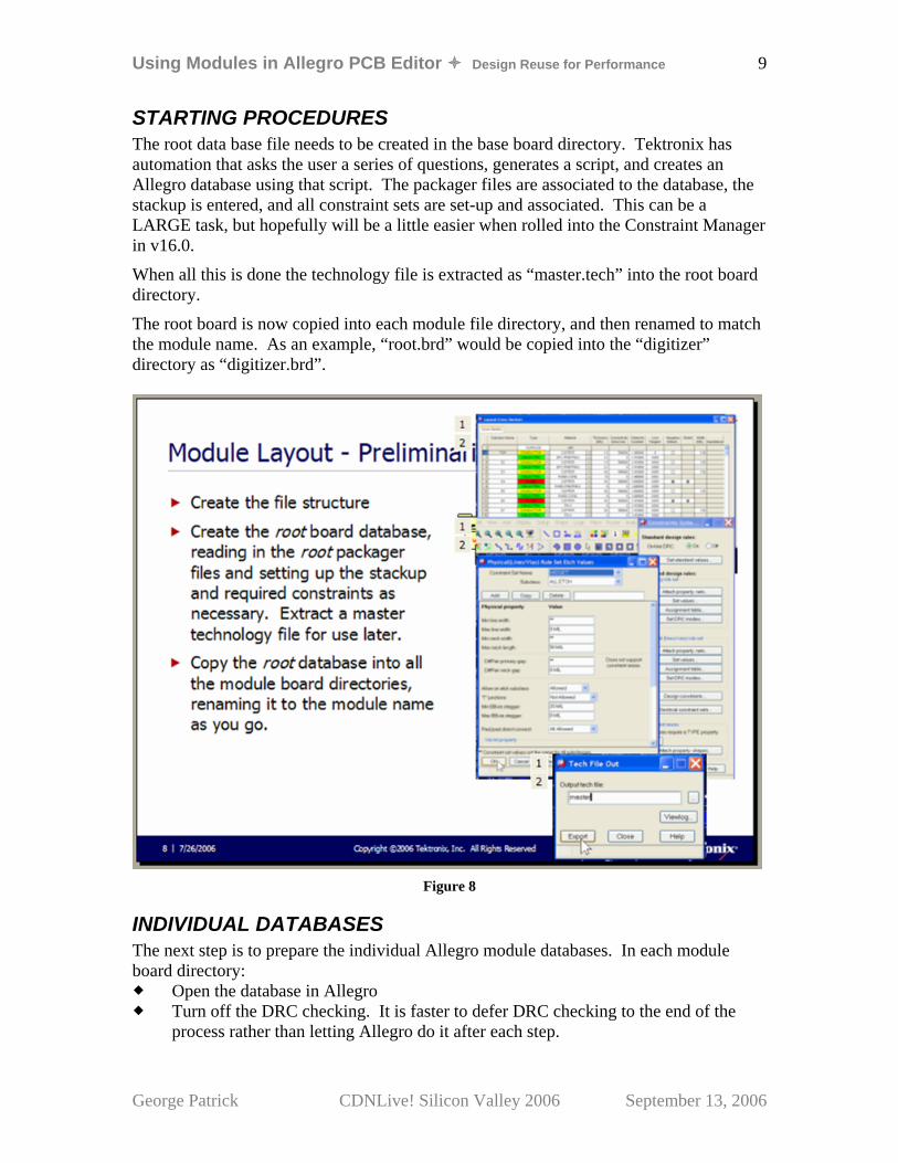
STARTING PROCEDURES The root data base file needs to be created in the base board directory. Tektronix has automation that asks the user a series of questions, generates a script, and creates an Allegro database using that script. The packager files are associated to the database, the stackup is entered, and all constraint sets are set-up and associated. This can be a LARGE task, but hopefully will be a little easier when rolled into the Constraint Manager in v16.0.
When all this is done the technology file is extracted as “master.tech” into the root board directory.
The root board is now copied into each module file directory, and then renamed to match the module name. As an example, “root.brd” would be copied into the “digitizer” directory as “digitizer.brd”.
Figure 8
INDIVIDUAL DATABASES The next step is to prepare the individual Allegro module databases. In each module board directory:
Open the database in Allegro Turn off the DRC checking. It is faster to defer DRC checking to the end of the
process rather than letting Allegro do it after each step.
George Patrick CDNLive! Silicon Valley 2006 September 13, 2006

Using Modules in Allegro PCB Editor Design Reuse for Performance 10
Import the appropriate packager files. Note the path, and that “Ignore FIXED property” and “Overwrite current constraints” are both checked. Ignoring the FIXED property is necessary in all modules that contain other modules as it is usual to fix any module that is inserted into another database file. It is done here to keep the process identical whether done at the beginning (when there is nothing to BE fixed), or later as the inevitable changes are done. Overwriting the existing constraints is done because we need the module constraints acting on the database constraints instead the root board constraints. This can be adjusted as the designer prefers on later imports.
Figure 9
We now run DBDoctor, making sure that “Update all DRC (including batch)” and “Check shape outlines” is checked. This will also reset the “No DRC” checkbox and re-enable on-line DRC when it has completed. This can be quite time consuming on larger modules.
Finally, the database is saved and the whole process is repeated for the next module database.
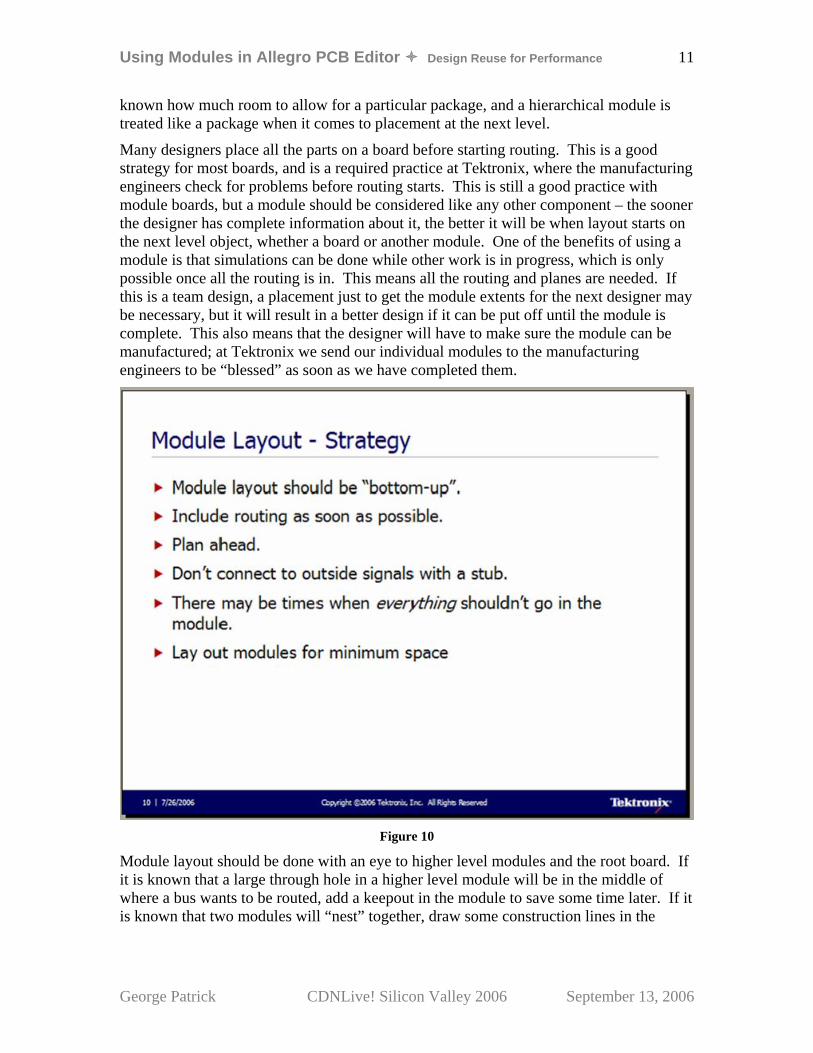
STRATEGY Module layout should be “bottom-up.” In other words, the lowest level module layout in a hierarchy should be completed before the next module starts. If there are two modules at the same level, they should both be completed. It is easier to lay out a circuit if it is
George Patrick CDNLive! Silicon Valley 2006 September 13, 2006
Using Modules in Allegro PCB Editor Design Reuse for Performance 11
known how much room to allow for a particular package, and a hierarchical module is treated like a package when it comes to placement at the next level.
Many designers place all the parts on a board before starting routing. This is a good strategy for most boards, and is a required practice at Tektronix, where the manufacturing engineers check for problems before routing starts. This is still a good practice with module boards, but a module should be considered like any other component – the sooner the designer has complete information about it, the better it will be when layout starts on the next level object, whether a board or another module. One of the benefits of using a module is that simulations can be done while other work is in progress, which is only possible once all the routing is in. This means all the routing and planes are needed. If this is a team design, a placement just to get the module extents for the next designer may be necessary, but it will result in a better design if it can be put off until the module is complete. This also means that the designer will have to make sure the module can be manufactured; at Tektronix we send our individual modules to the manufacturing engineers to be “blessed” as soon as we have completed them.
Figure 10
Module layout should be done with an eye to higher level modules and the root board. If it is known that a large through hole in a higher level module will be in the middle of where a bus wants to be routed, add a keepout in the module to save some time later. If it is known that two modules will “nest” together, draw some construction lines in the
George Patrick CDNLive! Silicon Valley 2006 September 13, 2006

Using Modules in Allegro PCB Editor Design Reuse for Performance 12
module database where parts need to fit. It probably isn’t possible to pre-plan where all obstructions are, catching some of them early is still better than catching them later.
Modules will usually have to connect to signals outside of themselves. Early on we connected these signals by running a line to the edge of the module and connecting to this line at the higher levels. This was a mistake: When changes were made to the module the whole line disappeared when the module was refreshed (both the line inside the module and the line connecting to it). Although this is now fixed in Allegro, we have found it is still a much better practice to connect outside signals to vias or thru-pins, as it allows more options and flexibility when connecting to the module.
There are cases where it makes more sense to do some of the routing outside the module, especially with busses. When a bus goes to all the modules in a hierarchy, routing inside the module may cause the bus to have the wrong topology. Again, advance planning may show that the bus should be routed on the board.
Modules need to use minimum space layout techniques even though there may be a lot of room on the board. The module may be used by others for their board designs, and they may not have the room you do. Be kind and do the work in your module instead of making them do extra work to fit your module in.
PLACE & ROUTE
Figure 11
George Patrick CDNLive! Silicon Valley 2006 September 13, 2006

Using Modules in Allegro PCB Editor Design Reuse for Performance 13
♦ Read in the master technology file. Of course if this is the first time this database has been worked on the current technology file will be fine, but it is a good idea to get in the habit of loading a new file just after the board is opened. Manipulate on-line DRC as before to speed things as much as possible.
♦ Place the modules and parts that need to be placed inside the module. There may be cases where some of the parts in the module should not be placed inside the module. An example of these parts would be heatsinks, mounting holes, or other hardware which may need to be manipulated in mechanical CAD programs and imported via IDF into the root board. That’s OK; any part not placed in the module will be available to be placed at higher levels. When placement is complete, FIX any modules so that connect lines will not be slid or “bubbled” while routing. There is also a new LOCK property in version 15.5.1, but I haven’t tried it yet in production and so don’t want to comment on it. Make any changes needed to the constraints (adding constraint areas, etc.) as they need to be made, but remember to export the technology file each time changes are made so it can be imported into the other modules and into the root board.
♦ Route as usual, adjusting and exporting the tech file as necessary.
♦ If planning to simulate the individual module, it will be necessary to have power and ground planes in place. If the plane splits are complex inside the module, it is probably a good idea to route the anti-etch lines now and connect them together at higher levels. Any planes generated here to aid simulation will not be used when creating the module, just the anti-etch.
♦ It is important to get as many changes as possible done to the layout now, rather than later. The module needs to be as close to the finished product as possible, as changes once later modules have been completed are much more painful than they will be now.
♦ Adjust reference designators text locations, remembering that they will be longer in the final board than in the module. Any adjustments make here will save time on the root board, but we have found they update reliably only in version 15.5.1 (we never used 15.5, and can’t comment on it).
♦ Run DBDoctor with all options checked.
George Patrick CDNLive! Silicon Valley 2006 September 13, 2006
Using Modules in Allegro PCB Editor Design Reuse for Performance 14
CREATING MODULES
Figure 12
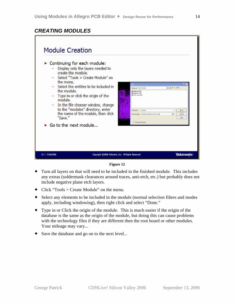
Turn all layers on that will need to be included in the finished module. This includes any extras (soldermask clearances around traces, anti-etch, etc.) but probably does not include negative plane etch layers.
Click “Tools > Create Module” on the menu.
Select any elements to be included in the module (normal selection filters and modes apply, including windowing), then right click and select “Done.”
Type in or Click the origin of the module. This is much easier if the origin of the database is the same as the origin of the module, but doing this can cause problems with the technology files if they are different then the root board or other modules. Your mileage may vary...
Save the database and go on to the next level...
George Patrick CDNLive! Silicon Valley 2006 September 13, 2006

Using Modules in Allegro PCB Editor Design Reuse for Performance 15
CHANGES
Figure 13
If it is found that a connect line, shape, or package inside a placed module must be moved, the correction must be done to the module’s database and then updated to any database in which the module is used. The easiest method is to try the changes in the current database (UNFIXING the affected module first), and then opening the affected module’s database and making the changes there once they are proven, perhaps exporting a sub-design from the original database and importing them into the module. Save the new database and module, and then update the placed modules in the original database. Be sure to update the technology file when opening the module database, and update the tech file if changes were made to the constraints. Any other databases where the module is used as a standalone entity need to be updated at this point, too.
This is a VERY time consuming process, especially if a change needs to make in the lowest level module of a hierarchical module design. This “extra” time needs be accounted for when estimating project time, and is the reason that doing the layout for 80% of the board in 25% of the time doesn’t happen in reality. It is important to communicate to engineers and project managers that the time needed to complete the project may not follow their expectations, and that every change made to a module may require unexpectedly (to them) long times implement. This is also why each module needs to be as close to a finished state as possible before continuing to the next level module or to the root board.
George Patrick CDNLive! Silicon Valley 2006 September 13, 2006

Using Modules in Allegro PCB Editor Design Reuse for Performance 16
Let me add that Cadence’s licensing makes this process rather expensive, too. It seems a little silly to have to use two licenses just because the software requires you to have two windows open as part of the editing process, one for the board and one for the module.
Figure 14
Changing the stackup is like changing parts in every module, except worse. Not only is it necessary to perform the change, read in the tech file, resave, and update every database and module file in the board; possible DRC errors due to changes in line widths, clearances, and other issues must be cleared as well. This is more time consuming than any other change.
Let me reiterate: locking down the stackup early and planning ahead is going to save time, headaches, and finger-pointing when the board is done.
ARCHIVING Archiving is in preliminary state at Tektronix, but a word about plans in place is in order.
George Patrick CDNLive! Silicon Valley 2006 September 13, 2006

Using Modules in Allegro PCB Editor Design Reuse for Performance 17
Figure 15
Designs are submitted to a MatrixOne application that places the appropriate files in the required locations and notifies people when required steps in the manufacturing and purchasing process need to be done. Part of this process is extraction of the module files and databases and creation of a page where they can be viewed and searched. The engineers are responsible for including a short text file (or manually entering the information) that contains a brief “keyword” description of the module for search purposes; the layout designer includes a similar file for the physical module. The search engine targets specific words and web addresses containing the full descriptive text and PDF versions of the schematic and manufacturing files are linked using commercial search engine technology.
Advertising this capability is probably necessary for design reuse to be fully embraced company wide. In any global operation this is the hardest part, as word of mouth doesn’t work when the engineers are literally on opposite sides of the earth.
George Patrick CDNLive! Silicon Valley 2006 September 13, 2006