using circuit simulators - eas.uccs.edueas.uccs.edu/~mwickert/ece5250/notes/cktsim.pdfadvanced...
TRANSCRIPT

Advanced Design System 2009 - Using Circuit Simulators
1
ADS 2009February 2009
Using Circuit Simulators

Advanced Design System 2009 - Using Circuit Simulators
2
© Agilent Technologies, Inc. 2000-20095301 Stevens Creek Blvd., Santa Clara, CA 95052 USANo part of this documentation may be reproduced in any form or by any means (includingelectronic storage and retrieval or translation into a foreign language) without prioragreement and written consent from Agilent Technologies, Inc. as governed by UnitedStates and international copyright laws.
AcknowledgmentsMentor Graphics is a trademark of Mentor Graphics Corporation in the U.S. and othercountries. Microsoft®, Windows®, MS Windows®, Windows NT®, and MS-DOS® are U.S.registered trademarks of Microsoft Corporation. Pentium® is a U.S. registered trademarkof Intel Corporation. PostScript® and Acrobat® are trademarks of Adobe SystemsIncorporated. UNIX® is a registered trademark of the Open Group. Java™ is a U.S.trademark of Sun Microsystems, Inc. SystemC® is a registered trademark of OpenSystemC Initiative, Inc. in the United States and other countries and is used withpermission. MATLAB® is a U.S. registered trademark of The Math Works, Inc.. HiSIM2source code, and all copyrights, trade secrets or other intellectual property rights in and tothe source code in its entirety, is owned by Hiroshima University and STARC.
The following third-party libraries are used by the NlogN Momentum solver:
"This program includes Metis 4.0, Copyright © 1998, Regents of the University ofMinnesota", http://www.cs.umn.edu/~metis , METIS was written by George Karypis([email protected]).
Intel@ Math Kernel Library, http://www.intel.com/software/products/mkl
SuperLU_MT version 2.0 - Copyright © 2003, The Regents of the University of California,through Lawrence Berkeley National Laboratory (subject to receipt of any requiredapprovals from U.S. Dept. of Energy). All rights reserved. SuperLU Disclaimer: THISSOFTWARE IS PROVIDED BY THE COPYRIGHT HOLDERS AND CONTRIBUTORS "AS IS"AND ANY EXPRESS OR IMPLIED WARRANTIES, INCLUDING, BUT NOT LIMITED TO, THEIMPLIED WARRANTIES OF MERCHANTABILITY AND FITNESS FOR A PARTICULAR PURPOSEARE DISCLAIMED. IN NO EVENT SHALL THE COPYRIGHT OWNER OR CONTRIBUTORS BELIABLE FOR ANY DIRECT, INDIRECT, INCIDENTAL, SPECIAL, EXEMPLARY, ORCONSEQUENTIAL DAMAGES (INCLUDING, BUT NOT LIMITED TO, PROCUREMENT OFSUBSTITUTE GOODS OR SERVICES; LOSS OF USE, DATA, OR PROFITS; OR BUSINESSINTERRUPTION) HOWEVER CAUSED AND ON ANY THEORY OF LIABILITY, WHETHER INCONTRACT, STRICT LIABILITY, OR TORT (INCLUDING NEGLIGENCE OR OTHERWISE)ARISING IN ANY WAY OUT OF THE USE OF THIS SOFTWARE, EVEN IF ADVISED OF THEPOSSIBILITY OF SUCH DAMAGE.
AMD Version 2.2 - AMD Notice: The AMD code was modified. Used by permission. AMDcopyright: AMD Version 2.2, Copyright © 2007 by Timothy A. Davis, Patrick R. Amestoy,and Iain S. Duff. All Rights Reserved. AMD License: Your use or distribution of AMD or anymodified version of AMD implies that you agree to this License. This library is freesoftware; you can redistribute it and/or modify it under the terms of the GNU LesserGeneral Public License as published by the Free Software Foundation; either version 2.1 ofthe License, or (at your option) any later version. This library is distributed in the hopethat it will be useful, but WITHOUT ANY WARRANTY; without even the implied warranty of

Advanced Design System 2009 - Using Circuit Simulators
3
MERCHANTABILITY or FITNESS FOR A PARTICULAR PURPOSE. See the GNU LesserGeneral Public License for more details. You should have received a copy of the GNULesser General Public License along with this library; if not, write to the Free SoftwareFoundation, Inc., 51 Franklin St, Fifth Floor, Boston, MA 02110-1301 USA Permission ishereby granted to use or copy this program under the terms of the GNU LGPL, providedthat the Copyright, this License, and the Availability of the original version is retained onall copies.User documentation of any code that uses this code or any modified version ofthis code must cite the Copyright, this License, the Availability note, and "Used bypermission." Permission to modify the code and to distribute modified code is granted,provided the Copyright, this License, and the Availability note are retained, and a noticethat the code was modified is included. AMD Availability:http://www.cise.ufl.edu/research/sparse/amd
UMFPACK 5.0.2 - UMFPACK Notice: The UMFPACK code was modified. Used by permission.UMFPACK Copyright: UMFPACK Copyright © 1995-2006 by Timothy A. Davis. All RightsReserved. UMFPACK License: Your use or distribution of UMFPACK or any modified versionof UMFPACK implies that you agree to this License. This library is free software; you canredistribute it and/or modify it under the terms of the GNU Lesser General Public Licenseas published by the Free Software Foundation; either version 2.1 of the License, or (atyour option) any later version. This library is distributed in the hope that it will be useful,but WITHOUT ANY WARRANTY; without even the implied warranty of MERCHANTABILITYor FITNESS FOR A PARTICULAR PURPOSE. See the GNU Lesser General Public License formore details. You should have received a copy of the GNU Lesser General Public Licensealong with this library; if not, write to the Free Software Foundation, Inc., 51 Franklin St,Fifth Floor, Boston, MA 02110-1301 USA Permission is hereby granted to use or copy thisprogram under the terms of the GNU LGPL, provided that the Copyright, this License, andthe Availability of the original version is retained on all copies. User documentation of anycode that uses this code or any modified version of this code must cite the Copyright, thisLicense, the Availability note, and "Used by permission." Permission to modify the codeand to distribute modified code is granted, provided the Copyright, this License, and theAvailability note are retained, and a notice that the code was modified is included.UMFPACK Availability: http://www.cise.ufl.edu/research/sparse/umfpack UMFPACK(including versions 2.2.1 and earlier, in FORTRAN) is available athttp://www.cise.ufl.edu/research/sparse . MA38 is available in the Harwell SubroutineLibrary. This version of UMFPACK includes a modified form of COLAMD Version 2.0,originally released on Jan. 31, 2000, also available athttp://www.cise.ufl.edu/research/sparse . COLAMD V2.0 is also incorporated as a built-infunction in MATLAB version 6.1, by The MathWorks, Inc. http://www.mathworks.com .COLAMD V1.0 appears as a column-preordering in SuperLU (SuperLU is available athttp://www.netlib.org ). UMFPACK v4.0 is a built-in routine in MATLAB 6.5. UMFPACK v4.3is a built-in routine in MATLAB 7.1.
Errata The ADS product may contain references to "HP" or "HPEESOF" such as in filenames and directory names. The business entity formerly known as "HP EEsof" is now partof Agilent Technologies and is known as "Agilent EEsof". To avoid broken functionality andto maintain backward compatibility for our customers, we did not change all the namesand labels that contain "HP" or "HPEESOF" references.
Warranty The material contained in this document is provided "as is", and is subject tobeing changed, without notice, in future editions. Further, to the maximum extentpermitted by applicable law, Agilent disclaims all warranties, either express or implied,

Advanced Design System 2009 - Using Circuit Simulators
4
with regard to this documentation and any information contained herein, including but notlimited to the implied warranties of merchantability and fitness for a particular purpose.Agilent shall not be liable for errors or for incidental or consequential damages inconnection with the furnishing, use, or performance of this document or of anyinformation contained herein. Should Agilent and the user have a separate writtenagreement with warranty terms covering the material in this document that conflict withthese terms, the warranty terms in the separate agreement shall control.
Technology Licenses The hardware and/or software described in this document arefurnished under a license and may be used or copied only in accordance with the terms ofsuch license. Portions of this product include the SystemC software licensed under OpenSource terms, which are available for download at http://systemc.org/ . This software isredistributed by Agilent. The Contributors of the SystemC software provide this software"as is" and offer no warranty of any kind, express or implied, including without limitationwarranties or conditions or title and non-infringement, and implied warranties orconditions merchantability and fitness for a particular purpose. Contributors shall not beliable for any damages of any kind including without limitation direct, indirect, special,incidental and consequential damages, such as lost profits. Any provisions that differ fromthis disclaimer are offered by Agilent only.
Restricted Rights Legend U.S. Government Restricted Rights. Software and technicaldata rights granted to the federal government include only those rights customarilyprovided to end user customers. Agilent provides this customary commercial license inSoftware and technical data pursuant to FAR 12.211 (Technical Data) and 12.212(Computer Software) and, for the Department of Defense, DFARS 252.227-7015(Technical Data - Commercial Items) and DFARS 227.7202-3 (Rights in CommercialComputer Software or Computer Software Documentation).

Advanced Design System 2009 - Using Circuit Simulators
5
Simulation Basics . . . . . . . . . . . . . . . . . . . . . . . . . . . . . . . . . . . . . . . . . . . . . . . . . . . . . . . . 7 Simulation Types . . . . . . . . . . . . . . . . . . . . . . . . . . . . . . . . . . . . . . . . . . . . . . . . . . . . . . . 7 Common Simulation Usage . . . . . . . . . . . . . . . . . . . . . . . . . . . . . . . . . . . . . . . . . . . . . . . . 9 Working with the Examples Directory . . . . . . . . . . . . . . . . . . . . . . . . . . . . . . . . . . . . . . . . 10 The Simulation Process . . . . . . . . . . . . . . . . . . . . . . . . . . . . . . . . . . . . . . . . . . . . . . . . . . 11 Using the Schematic Wizard . . . . . . . . . . . . . . . . . . . . . . . . . . . . . . . . . . . . . . . . . . . . . . . 12 Using the Smart Simulation Wizard . . . . . . . . . . . . . . . . . . . . . . . . . . . . . . . . . . . . . . . . . . 30 Selecting Simulation Controllers . . . . . . . . . . . . . . . . . . . . . . . . . . . . . . . . . . . . . . . . . . . . 33 Using the Simulator Options Component . . . . . . . . . . . . . . . . . . . . . . . . . . . . . . . . . . . . . . 34 Using the Simulation Setup Dialog . . . . . . . . . . . . . . . . . . . . . . . . . . . . . . . . . . . . . . . . . . . 44 Sweeping Parameters . . . . . . . . . . . . . . . . . . . . . . . . . . . . . . . . . . . . . . . . . . . . . . . . . . . 50 Optimizing a Design . . . . . . . . . . . . . . . . . . . . . . . . . . . . . . . . . . . . . . . . . . . . . . . . . . . . . 51 Working with Expressions . . . . . . . . . . . . . . . . . . . . . . . . . . . . . . . . . . . . . . . . . . . . . . . . . 51 Running a Simulation and Controlling Simulation Data . . . . . . . . . . . . . . . . . . . . . . . . . . . . . 52 Displaying Simulation Parameters on the Schematic . . . . . . . . . . . . . . . . . . . . . . . . . . . . . . 60 Controlling a Simulation . . . . . . . . . . . . . . . . . . . . . . . . . . . . . . . . . . . . . . . . . . . . . . . . . . 61 Simulating from a Layout . . . . . . . . . . . . . . . . . . . . . . . . . . . . . . . . . . . . . . . . . . . . . . . . . 61 Viewing DC Solutions . . . . . . . . . . . . . . . . . . . . . . . . . . . . . . . . . . . . . . . . . . . . . . . . . . . . 62 Displaying Simulation Results . . . . . . . . . . . . . . . . . . . . . . . . . . . . . . . . . . . . . . . . . . . . . . 63 Reusing Simulation Solutions . . . . . . . . . . . . . . . . . . . . . . . . . . . . . . . . . . . . . . . . . . . . . . 64 Analog/RF Simulation Computations and Convergence Criteria . . . . . . . . . . . . . . . . . . . . . . . 65
Using Circuit Simulators for RF System Analysis . . . . . . . . . . . . . . . . . . . . . . . . . . . . . . . . . . . 70 Applicable Simulation Components . . . . . . . . . . . . . . . . . . . . . . . . . . . . . . . . . . . . . . . . . . 70 Applicable Measurements . . . . . . . . . . . . . . . . . . . . . . . . . . . . . . . . . . . . . . . . . . . . . . . . . 71 Fundamentals of Using Circuit Simulators for System Analysis . . . . . . . . . . . . . . . . . . . . . . . 72 Budget Analysis . . . . . . . . . . . . . . . . . . . . . . . . . . . . . . . . . . . . . . . . . . . . . . . . . . . . . . . 74 Using IMT-Based Mixer Models in Spurious Signal Analysis . . . . . . . . . . . . . . . . . . . . . . . . . . 93 System Noise Analysis . . . . . . . . . . . . . . . . . . . . . . . . . . . . . . . . . . . . . . . . . . . . . . . . . . . 97
Parameter Sweeps and Sweep Plans . . . . . . . . . . . . . . . . . . . . . . . . . . . . . . . . . . . . . . . . . . . 99 Conducting Sweeps . . . . . . . . . . . . . . . . . . . . . . . . . . . . . . . . . . . . . . . . . . . . . . . . . . . . . 99 Basic Procedures . . . . . . . . . . . . . . . . . . . . . . . . . . . . . . . . . . . . . . . . . . . . . . . . . . . . . . . 101 Recommendations and Tips . . . . . . . . . . . . . . . . . . . . . . . . . . . . . . . . . . . . . . . . . . . . . . . 107 SweepPlan Controller . . . . . . . . . . . . . . . . . . . . . . . . . . . . . . . . . . . . . . . . . . . . . . . . . . . 109 Parameter Sweep Controller . . . . . . . . . . . . . . . . . . . . . . . . . . . . . . . . . . . . . . . . . . . . . . 110
Working with Data Files . . . . . . . . . . . . . . . . . . . . . . . . . . . . . . . . . . . . . . . . . . . . . . . . . . . . 113 Supported Data Formats . . . . . . . . . . . . . . . . . . . . . . . . . . . . . . . . . . . . . . . . . . . . . . . . . 114 Making a Data File . . . . . . . . . . . . . . . . . . . . . . . . . . . . . . . . . . . . . . . . . . . . . . . . . . . . . . 115 Saving a Data File . . . . . . . . . . . . . . . . . . . . . . . . . . . . . . . . . . . . . . . . . . . . . . . . . . . . . . 116 Using Data Files, Datasets, and Data Access Components . . . . . . . . . . . . . . . . . . . . . . . . . . 116 Reading and Writing Data Files . . . . . . . . . . . . . . . . . . . . . . . . . . . . . . . . . . . . . . . . . . . . . 117 Examples . . . . . . . . . . . . . . . . . . . . . . . . . . . . . . . . . . . . . . . . . . . . . . . . . . . . . . . . . . . . 121 Touchstone SnP Format . . . . . . . . . . . . . . . . . . . . . . . . . . . . . . . . . . . . . . . . . . . . . . . . . . 121 ADS Impulse File Format . . . . . . . . . . . . . . . . . . . . . . . . . . . . . . . . . . . . . . . . . . . . . . . . . 134 Discrete Format . . . . . . . . . . . . . . . . . . . . . . . . . . . . . . . . . . . . . . . . . . . . . . . . . . . . . . . 139 Model MDIF Files . . . . . . . . . . . . . . . . . . . . . . . . . . . . . . . . . . . . . . . . . . . . . . . . . . . . . . . 141 PDF Format . . . . . . . . . . . . . . . . . . . . . . . . . . . . . . . . . . . . . . . . . . . . . . . . . . . . . . . . . . 143 S2PMDIF Format . . . . . . . . . . . . . . . . . . . . . . . . . . . . . . . . . . . . . . . . . . . . . . . . . . . . . . . 145 P2D Format . . . . . . . . . . . . . . . . . . . . . . . . . . . . . . . . . . . . . . . . . . . . . . . . . . . . . . . . . . 154 S2D Format . . . . . . . . . . . . . . . . . . . . . . . . . . . . . . . . . . . . . . . . . . . . . . . . . . . . . . . . . . 163 IMT Format . . . . . . . . . . . . . . . . . . . . . . . . . . . . . . . . . . . . . . . . . . . . . . . . . . . . . . . . . . . 175 SPW Format . . . . . . . . . . . . . . . . . . . . . . . . . . . . . . . . . . . . . . . . . . . . . . . . . . . . . . . . . . 179
Advanced Design System 2009 - Using Circuit Simulators
6
TIM Format . . . . . . . . . . . . . . . . . . . . . . . . . . . . . . . . . . . . . . . . . . . . . . . . . . . . . . . . . . . 180 Generic MDIF . . . . . . . . . . . . . . . . . . . . . . . . . . . . . . . . . . . . . . . . . . . . . . . . . . . . . . . . . 183 CITIfile Data Format . . . . . . . . . . . . . . . . . . . . . . . . . . . . . . . . . . . . . . . . . . . . . . . . . . . . 185
ADS Simulator Input Syntax . . . . . . . . . . . . . . . . . . . . . . . . . . . . . . . . . . . . . . . . . . . . . . . . 199 Setting Environment Variables . . . . . . . . . . . . . . . . . . . . . . . . . . . . . . . . . . . . . . . . . . . . . 199 Codewording and Security . . . . . . . . . . . . . . . . . . . . . . . . . . . . . . . . . . . . . . . . . . . . . . . . 201 Running a Simulation from the Command Line . . . . . . . . . . . . . . . . . . . . . . . . . . . . . . . . . . 201 General Syntax . . . . . . . . . . . . . . . . . . . . . . . . . . . . . . . . . . . . . . . . . . . . . . . . . . . . . . . . 203 The ADS Simulator Syntax . . . . . . . . . . . . . . . . . . . . . . . . . . . . . . . . . . . . . . . . . . . . . . . . 203 Instance Statements . . . . . . . . . . . . . . . . . . . . . . . . . . . . . . . . . . . . . . . . . . . . . . . . . . . . 209 Model Statements . . . . . . . . . . . . . . . . . . . . . . . . . . . . . . . . . . . . . . . . . . . . . . . . . . . . . . 210 Subnetwork Definitions . . . . . . . . . . . . . . . . . . . . . . . . . . . . . . . . . . . . . . . . . . . . . . . . . . 211 Expression Capability . . . . . . . . . . . . . . . . . . . . . . . . . . . . . . . . . . . . . . . . . . . . . . . . . . . . 212 C-Preprocessor . . . . . . . . . . . . . . . . . . . . . . . . . . . . . . . . . . . . . . . . . . . . . . . . . . . . . . . . 213 Data Access Component . . . . . . . . . . . . . . . . . . . . . . . . . . . . . . . . . . . . . . . . . . . . . . . . . . 215 Reserved Names and Name Spaces . . . . . . . . . . . . . . . . . . . . . . . . . . . . . . . . . . . . . . . . . . 216
Preparing a Circuit for Simulation in ADS . . . . . . . . . . . . . . . . . . . . . . . . . . . . . . . . . . . . . . . . 227 Using Current Probes . . . . . . . . . . . . . . . . . . . . . . . . . . . . . . . . . . . . . . . . . . . . . . . . . . . . 227 Naming Nodes . . . . . . . . . . . . . . . . . . . . . . . . . . . . . . . . . . . . . . . . . . . . . . . . . . . . . . . . 228 Using NodeSet and NodeSetByName Components . . . . . . . . . . . . . . . . . . . . . . . . . . . . . . . . 228 Highlighting Nodes . . . . . . . . . . . . . . . . . . . . . . . . . . . . . . . . . . . . . . . . . . . . . . . . . . . . 230 Using Constants, Variables, and Functions . . . . . . . . . . . . . . . . . . . . . . . . . . . . . . . . . . . . . 231 Applying Measurements . . . . . . . . . . . . . . . . . . . . . . . . . . . . . . . . . . . . . . . . . . . . . . . . . . 234 Using Simulation Templates . . . . . . . . . . . . . . . . . . . . . . . . . . . . . . . . . . . . . . . . . . . . . . . 236 Using Simulation Instrument Components . . . . . . . . . . . . . . . . . . . . . . . . . . . . . . . . . . . . . 239
S-Parameter Test Labs and Sequencer . . . . . . . . . . . . . . . . . . . . . . . . . . . . . . . . . . . . . . . . 240 Creating a Test Bench . . . . . . . . . . . . . . . . . . . . . . . . . . . . . . . . . . . . . . . . . . . . . . . . . . . 240 S-Parameter Test Labs . . . . . . . . . . . . . . . . . . . . . . . . . . . . . . . . . . . . . . . . . . . . . . . . . . . 244 Sequencer . . . . . . . . . . . . . . . . . . . . . . . . . . . . . . . . . . . . . . . . . . . . . . . . . . . . . . . . . . . 248 Using Measurement Equations with a Test Lab or Sequencer . . . . . . . . . . . . . . . . . . . . . . . . 251 Improving Test Lab Simulation Efficiency . . . . . . . . . . . . . . . . . . . . . . . . . . . . . . . . . . . . . . 252
RefNets . . . . . . . . . . . . . . . . . . . . . . . . . . . . . . . . . . . . . . . . . . . . . . . . . . . . . . . . . . . . . . . 253 RefNetTB Using an S-Parameter Test Lab . . . . . . . . . . . . . . . . . . . . . . . . . . . . . . . . . . . . . . 254 RefNetDesign - File Based Termination . . . . . . . . . . . . . . . . . . . . . . . . . . . . . . . . . . . . . . . 262
An ADS Simulation Example . . . . . . . . . . . . . . . . . . . . . . . . . . . . . . . . . . . . . . . . . . . . . . . . 264 Placing Circuit Sources . . . . . . . . . . . . . . . . . . . . . . . . . . . . . . . . . . . . . . . . . . . . . . . . . . . 264 Specifying Points for Collecting Data . . . . . . . . . . . . . . . . . . . . . . . . . . . . . . . . . . . . . . . . . 265 Selecting a Simulation Type . . . . . . . . . . . . . . . . . . . . . . . . . . . . . . . . . . . . . . . . . . . . . . . 266 Selecting a Sweep Type and Plan . . . . . . . . . . . . . . . . . . . . . . . . . . . . . . . . . . . . . . . . . . . 268 Setting Simulation Options . . . . . . . . . . . . . . . . . . . . . . . . . . . . . . . . . . . . . . . . . . . . . . . . 269 Modifying the Simulation Setup . . . . . . . . . . . . . . . . . . . . . . . . . . . . . . . . . . . . . . . . . . . . . 269 Starting the Simulation . . . . . . . . . . . . . . . . . . . . . . . . . . . . . . . . . . . . . . . . . . . . . . . . . . 270 Displaying Simulation Data . . . . . . . . . . . . . . . . . . . . . . . . . . . . . . . . . . . . . . . . . . . . . . . . 270

Advanced Design System 2009 - Using Circuit Simulators
7
Simulation BasicsThis documentation provides information that applies to the Analog/RF simulation in ADS.It also contains general information about the various simulation controllers that areavailable in ADS. Before using this documentation, you should see Advanced DesignSystem Quick Start (adstour) and Schematic Capture and Layout (usrguide) to review thewhole product.
For details about running an Analog/RF simulation, you should also see Preparing a Circuitfor Simulation in ADS (cktsim) and An ADS Simulation Example (cktsim), then continuewith other areas of the Simulation documentation that provide details about the simulationcontrollers.
Simulation Types ADS provides simulators that enable you to simulate circuits and RF systems designed forspecific objectives. The following table provides brief descriptions of the availablesimulation controllers. See the documentation for the Analog/RF simulation controllers forcomplete information about each one.

Advanced Design System 2009 - Using Circuit Simulators
8
Simulator Description
DC Fundamental to all simulations, it performs a topology check and an analysis of theDC operating point of a circuit. See DC Simulation (cktsimdc).
AC Obtains small-signal transfer parameters, such as voltage gain, current gain, andlinear noise voltage and currents. This simulator is useful in designing passive circuitsand small-signal active circuits such as low-noise amplifiers (LNAs). See ACSimulation (cktsimac).
S-parameter Provides linear S-parameters, linear noise parameters, transimpedance (Zij), and
transadmittance (Yij), by linearizing the circuit about the DC operating point and
performing a linear small-signal analysis that treats the circuit as a multiport. Eachport is turned on sequentially. S-parameters can be converted to Y- and Z-parameters. This simulator can be used to achieve many of the same design goals asthe AC simulator. See S-Parameter Simulation (cktsimsp).
Harmonic Balance Uses nonlinear harmonic-balance techniques to find the steady-state solution in thefrequency domain. This simulator is useful in designing RF amplifiers, mixers, andoscillators. A Krylov subspace technique is available to reduce memory requirementsand increase the speed of solution. This option is useful in designing large RFintegrated circuits or RF/IF subsystems, where a large number of devices or largenumbers of harmonics and intermodulation products are involved. See HarmonicBalance Simulation (cktsimhb).
Large-signal S-parameter (LSSP)
A type of harmonic balance simulation, it performs large-signal S-parameter analysesto represent the nonlinear behavior of items such as power amplifiers. Theaccompanying P2D simulator available in ADS can be used to speed up subsequentanalyses. See Large-Signal S-Parameter Simulation (cktsimlssp).
P2D Generates a .p2d file that can be used to describe the behavior of a file-basedcomponent (such as the AmplifierP2D component, available in the System-Amps &Mixers library). See P2D Simulation (cktsimp2d).
Gain Compression(XdB)
Seeks a user-defined gain-compression point at which an actual power curve deviatesfrom an idealized linear power curve. This is useful in power amplifier design. SeeGain Compression Simulation (cktsimgain).
Circuit Envelope Uses a combination of frequency- and time-domain analysis techniques to yield a fastand complete analysis of complex signals such as digitally modulated RF signals. Itrepresents input waveforms as RF carriers with modulation envelopes that aredescribed in the time domain. This is useful in designing circuits and systemsinvolving modulators/demodulators or complex modulated signals. See CircuitEnvelope Simulation (cktsimenv).
Transient/Convolution Solves a nonlinear circuit in the time domain, and linear components can besimulated by means of convolution or a simplified equivalent-circuit model. SeeTransient and Convolution Simulation (cktsimtrans).
RF System BudgetAnalysis
Determines the linear and nonlinear characteristics of an RF system comprising acascade of two-port linear or nonlinear components. The RF system may also includeautomatic gain control (AGC) loops to control gain and set power levels at specificpoints in the RF system. See RF System Budget Analysis (rfsysbudget).
About Licensing
These simulators require licenses to run a simulation. Confirm that the simulator ofinterest is included with your purchase. ADS allows you to create a circuit, but if you donot have the correct license you will not be able to simulate it.

Advanced Design System 2009 - Using Circuit Simulators
9
Common Simulation UsageThe following table describes some common design objectives and the simulators thatwould be appropriate to each. The simulators are listed in the order they would generallybe applied.
Simulator used for Various Design Types

Advanced Design System 2009 - Using Circuit Simulators
10
Design Simulator Comments
Filter DC
AC
S-parameter
Mixer DC
AC Test for AC frequency conversion (also known as frequency-convertingAC, or FCAC).Applies to system mixer models only.
HarmonicBalance
Select nonlinear noise option to obtain noise figure.
Transient
Envelope
XDB
Power amplifier DC
AC
S-parameter
HarmonicBalance
Test for load-pull characteristics.
LSSP Also use the P2D simulator to generate a .p2d file.
XDB Find gain-compression point.
Transient
Envelope Find ACPR (adjacent-channel power ratio).
Transceiver DC
AC Test for AC frequency conversion (FCAC).
HarmonicBalance
Envelope
Budget RF system must be a cascade of two-port components.
Oscillator DC
S-parameter
HarmonicBalance
Check for power spectra and phase noise.
Envelope Check for startup switching.
Phase-lockedloop
Envelope Check for transient responses.
Working with the Examples Directory ADS includes example projects containing designs that you can open and run.
Most of the designs discussed in this documentation are available in the location whereyou installed ADS, typically $HPEESOF_DIR/examples directory. For detailed informationabout locating and opening ADS example projects, see Schematic Capture and Layout

Advanced Design System 2009 - Using Circuit Simulators
11
(usrguide). For documentation on ADS examples organized by application, see theExamples Documentation.
Briefly, here is how to get started using examples. ADS examples include projects andtemplates. On UNIX, these projects are read-only directories. To work with an exampleproject, you must first make a copy in a directory for which you have write permission.Windows users should also copy these examples to preserve the integrity of the examples.For convenience in keeping track of designs, you may want to create directory names thatmirror those in the examples directory.
Do not copy projects by using your operating system alone. Use these methods:
Use the Copy Project command in the Main window to copy entire projects to yourlocal directory.Copy projects as part of the software installation procedure.
This ensures that all files that are part of the project are copied.
The Simulation Process The following list shows the basic simulation process, and the sections to see for moreinformation:
Create your schematic, then add current probes and wire/pin labels to identify thenodes from which you want to collect data.Select a simulation method, specifying parameters as necessary. The parameters youspecify are based on the type of simulation you choose, the simulation options yourequire, and whether you're sweeping parameters, using expressions, and optimizingyour design.Selecting Simulation ControllersUsing the Simulator Options ComponentSweeping ParametersWorking with ExpressionsSelect a name for the dataset. This is where the simulation data will be saved.Running a Simulation and Controlling Simulation Data.Run the simulation.Controlling a SimulationView DC data by annotating the schematic with DC solutions and by viewing brief ordetailed device operating point data.Viewing DC SolutionsDisplay additional results using the Data Display.Displaying Simulation ResultsOptimize and tune a design.Displaying Simulation ResultsFor complete information, see Tuning, Optimization, and Statistical Design (optstat).
These are the basic steps. It is possible to develop very detailed, complex simulations, butthe process, for the most part, remains the same. The remainder of this section gives anoverview of these steps. If you are new to using ADS, or you use it infrequently, two

Advanced Design System 2009 - Using Circuit Simulators
12
wizards are available to help you with several steps in the process:
Using the Schematic Wizard follows the standard ADS use-model to help you withdesign creation and setting up a simulation.Using the Smart Simulation Wizard requires an existing design, and helps yousequence several simulations on the same device.
These wizards provide different features which may determine which one you prefer touse. The Schematic Wizard helps you develop a design and prepares it for a simulation asif you are working directly in the design environment. The Smart Simulation Wizardrequires that you already have a design available and adds a Smart Simulation module forsequencing simulations to the design. The following table presents additional differences:
Comparison of Schematic Wizard to Smart Simulation Wizard
Schematic Wizard Smart Simulation Wizard
Sets up the initial schematic, but does not includesimulation sequencing, allowing support for moreapplication types.
Has two major features:
Set up initial schematic.Simulation sequencing on a common device undertest.
Uses the standard ADS use-model for schematicdevelopment.
Simulation sequencing is a non-standard use-model inADS.
Allows selection of application categories andapplies to more application types.
Simulation sequencing is limited to certain types ofdevices under test, and is not generally extendable to allapplication categories.
Provides selection by application, and includesschematics by simulation-type.
Does not include selection of simulation-type.
Assists with some schematic corrections whensimulation errors appear.
Does not include error correction.
Using the Schematic Wizard The Schematic Wizard is provided to assist new ADS users or those who use itinfrequently in performing the basic steps associated with schematic creation. Two optionsfor schematic creation are available:
Creating a design in the schematic that can be used as a component or subnetworkin another ADS design.Setting up a simulation based on a desired application or simulation type. Theschematic can include an existing or sample test circuit, or simply provide asimulation schematic into which a test circuit can be placed.
The Schematic Wizard guides you through a sequence of steps gathering information fromyou about the type of schematic you want to create. Based on your inputs, the wizardautomatically creates the specified schematic components. The wizard then provides youwith instructions for completing the schematic manually, and for invoking the simulatorwhen applicable. The simulations are set up to automatically display the results after

Advanced Design System 2009 - Using Circuit Simulators
13
successful simulations.
Accessing the Schematic Wizard
Access to the Schematic Wizard is controlled by the Schematic Wizard and Create InitialSchematic Window preference options. You can set these options in the Main Preferencedialog (in the ADS Main window: Tools > Preferences ). The Schematic Wizardautomatically appears when you perform certain actions related to the Schematic window.
NoteThe Schematic Wizard is not available for designs manipulated through any Layout window.
Starting a New Project
When you start a new project within ADS, the Schematic Wizard will appear if you haveselected both preferences Schematic Wizard and Create Initial Schematic Window.
Opening a New Schematic Window from Main
When you open a new Schematic window from the ADS Main window (using the toolbarbutton or Window > New Schematic ), the Schematic Wizard will appear if you haveselected the Schematic Wizard preference. The wizard will not appear if the newSchematic window is requested from an existing Schematic or Layout window.
New Design
Requesting a new design from any ADS window opens the New Design dialog. This dialogalso contains a Schematic Wizard option. (This option is not accessible when a new designis opened from any Layout window.) If the wizard option is selected, the SchematicWizard will open after you click OK in the New Design dialog. The default setting for theSchematic Wizard option is controlled by its preference setting in the Main Preferencedialog. If it is selected in the Main Preference dialog, it will be checked by default in theNew Design dialog.
When setting the design content options, the Schematic Wizard and Schematic DesignTemplates cannot be used at the same time since they both place components on theSchematic. Therefore, selecting the Schematic Wizard option automatically clears anyrequest for a Schematic Design Template. Similarly, requesting a Schematic DesignTemplate automatically clears the Schematic Wizard option.

Advanced Design System 2009 - Using Circuit Simulators
14
Simulation Error
If you run a simulation using a simulation schematic that is not properly configured, thesimulator will terminate with errors. If the Schematic Wizard option is selected, the wizardwill appear automatically after the simulation attempt has completed if the error occursdue to either of these reasons:
A schematic with an S-parameter simulation controller does not contain any validTerm components.The simulation schematic does not contain a valid simulation controller.
You can use the Schematic Wizard to help you correct the schematic. See Correcting an S-Parameter Simulation Schematic and Correcting a Simulation Schematic with NoSimulation Controller.
Schematic Wizard Start Page
When the Schematic Wizard appears, the Start page presents you with the followingchoices for proceeding with the schematic creation:
Circuit Helps you create a subnetwork that can be used as a component in anotherADS design. See Creating a Circuit.
Simulation Helps you set up a simulation and place a circuit to be simulated. See

Advanced Design System 2009 - Using Circuit Simulators
15
Creating a Simulation Schematic.
No help needed Dismisses the wizard.
When the Schematic Wizard is accessed by starting a new project or opening a newSchematic window, this page also offers the option Do not show this dialog again.Selecting this option will turn off the Schematic Wizard preference. You can select theSchematic Wizard preference option again in the Main Preferences dialog.
Schematic Wizard Navigation
The Schematic Wizard provides a navigation bar in the upper left corner of the window.This navigation bar indicates your progress through the steps required to complete theschematic setup, with a green box next to the current step. The steps on the navigationbar change depending on the options you select in the wizard.
Use the Back and Next buttons to move back and forth through the steps. The Backbutton is active for all steps except for Start. The Next button remains inactive for eachstep until you make a valid selection. When you have completed all required steps, usethe Finish button to initiate schematic creation. The final step also provides an option tohave instructions appear that assist you in the remainder of the schematic creationprocess. This option is persistent, so the setting for this option is the default the next timethe wizard is used.

Advanced Design System 2009 - Using Circuit Simulators
16
Creating a Circuit
Choosing the Circuit option from the Start page enables you to create a subnetwork thatcan be placed in another ADS design. Creating a subnetwork involves placing and namingports, and selecting a symbol that will represent the circuit. The steps associated with thischoice are:
Circuit SetupName PortsFinish
Circuit Setup Step
Network ports represent the connections of a circuit to the outside world. In this step ofthe design, you must specify how many ports you anticipate for your circuit. For example,if designing an amplifier from a transistor and passive components, the circuit might havean input, output, and bias connection. In this case, you should request three networkports.
A symbol is used to represent a subnetwork when it is placed within another ADS design.Each connection point on the symbol will correspond to one of the subnetwork ports. ADScan automatically generate a symbol for you based on the number of ports specified,which is achieved using the Use default symbol option. However, if you want your symbolto be representative of the underlying subnetwork, use the Allow symbol selection option.You will be provided with a large set of possible symbols from which to choose.

Advanced Design System 2009 - Using Circuit Simulators
17
Correctly specifying the number of ports at this stage of the process will ease the work increating the subnetwork. However, if you later determine that you must add or remove aport from the circuit, this can be done manually. It is important, however, that the changeis made to both the circuit design and the symbol in order for the subnetwork to functionproperly.
Naming Ports Step
Ports created in ADS assume default names of P1, P2, etc. However, to make the portdesignations more physically meaningful, it is possible to specify alternate names forthese ports. In this phase of the process, you may either use the default names providedor type in the desired names for each port.
If you chose the Use default symbol option in the Circuit Setup step, you are given theopportunity to determine whether or not you would like instructions to appear after thewizard has completed the setup. However, if you chose the Allow symbol selection option,this option regarding supplemental instructions is not available. In this case, theinstructions will be shown to help you create the custom symbol and return to theschematic view following symbol selection.
Finish Circuit Creation Step
Successful completion of the wizard leads to a starting design in which ports are placed. Ifyou chose to allow ADS to create a default symbol for you, you will see the requested

Advanced Design System 2009 - Using Circuit Simulators
18
number of ports placed on the schematic. You can view the symbol that has been createdfor you using the View > Create/Edit Schematic Symbol menu selection. If you go to thesymbol view, you can return to the schematic using the View > Create/Edit Schematicmenu selection. If you chose to have supplemental instructions provided, a dialog will alsoappear, similar to the following figure, containing these instructions. You can move thisdialog out of the way to interact with the schematic.
If you chose to create a custom symbol in the Circuit Setup step, the Symbol Generationdialog box appears with a selection of different symbols. You can scroll through theseselections and choose a suitable symbol. Be sure, however, that the number of pins on thesymbol matches the number of ports specified on the wizard. Once you have selected asymbol, you can return to the schematic view either using the Schematic button on theSchematic Wizard's instruction dialog or the View > Create/Edit Schematic menuselection. If you chose a symbol with a number of pins that does not match the specifiednumber of ports, you will be warned of this problem when you return to the schematicview provided that the dialog containing the instructions is currently visible.
In either case, once you are in the schematic view, you can create the appropriate designand connect it to the ports at the proper nodes in the circuit. Once the design has beensaved and provided a suitable name, it will be ready for placement in other designs.
Creating a Simulation Schematic
Choosing the Simulation option from the Schematic Wizard Start page enables you tocreate a schematic that will simulate the behavior of a sample or user-created circuit.Creating this schematic involves choosing the desired application, specifying the testcircuit, indicating the desired simulation type, and when appropriate, specifying how acircuit should be placed in the simulation schematic. The steps associated with creating asimulation schematic are:
ApplicationCircuit

Advanced Design System 2009 - Using Circuit Simulators
19
Simulation SetupFinish
Application Selection Step

Advanced Design System 2009 - Using Circuit Simulators
20
The first step in creating a simulation schematic is choosing the application type. A varietyof different choices representing common applications are provided. If you find yourintended application on the list, you can select it. If you do not see your application, theSchematic Wizard may still be able to provide assistance in creating your schematic.Simply choose the Other Application (not listed) option at the bottom of the tree.
HintThe wizard will not allow you to proceed until you have made a valid selection from the list. Top-levelitems in the tree structure that have sub-items beneath them are not valid selections.
Circuit Selection Step

Advanced Design System 2009 - Using Circuit Simulators
21
Once you have determined the application type, you are ready to specify the circuit thatwill be simulated within the schematic. Three options are provided relative to the testcircuit:
Use sample design A sample circuit appropriate for the application is provided. Thiscircuit will be copied into your project directory and connected into the simulationschematic.Use existing design Enables you to specify an existing ADS subnetwork (created,for example, using the Circuit option of the Schematic Wizard ) for placement withinthe simulation schematic. All designs in the current project will be shown. However, ifyou select a design that has not been properly created for use as a subnetwork, awarning will be issued and the design will be deselected. If you have a design withinanother project that you would like to use, you can copy it into the current projectusing the Copy Design from Another Project button.I will design my own circuit No test circuit will be placed in the simulationschematic. It is assumed that you will design your own circuit and manually connectit into the schematic created by the wizard.
The availability of each option is dependent on the selection made at prior steps.
HintThe wizard will not allow you to proceed until you have made a valid selection.
Simulation Setup Step

Advanced Design System 2009 - Using Circuit Simulators
22
You are now prepared to specify the type of simulation that you would like to complete.Based on prior selections, a list of possible simulations is offered. If you could not findyour desired application earlier ( Other Application ), then at this stage you are presentedwith a tree structure of common simulations as well as system and user-definedsimulation templates. The Description area below the list of simulations helps you tochoose from the different simulation options.
HintThe wizard will not allow you to proceed until you have made a valid selection.
Port Specification Step

Advanced Design System 2009 - Using Circuit Simulators
23
If you chose Use existing design in the Circuit Selection step, and you have selected avalid design to use as a test circuit within your simulation schematic, the Port Specificationstep is added. You must use this step to indicate what each of the pins on the componentrefers to within the subnetwork. Based upon application/simulation selections, you will begiven a list of possible designations for each port. Using the pull-down list, specify theappropriate port type. If you do not see the port type listed, you can choose either toground the port or leave it unconnected (open circuit termination). The circuit will beplaced on the schematic at this point so that you can visually inspect it to assist in theport designation.
HintUsing the Back button at this step will remove the placed circuit from the schematic.
Schematic Completion Step
Successful completion of the wizard leads to a schematic that is nearly ready forsimulation. If you requested that instructions be provided in the Simulation Setup step, adialog will appear with information to assist you in performing the specific tasks associatedwith completing your design, simulating the circuit, and viewing the simulation results.
ImportantBe sure to save the design if you want to preserve it.

Advanced Design System 2009 - Using Circuit Simulators
24
If you chose to use a simulation template (obtained using the Other Application path), youmust manually connect the test circuit (if specified) into the simulation schematic. Sometemplates may already have a test circuit included, in which case you can either use theexisting test circuit or delete it and put the specified test circuit placed by the wizard in itsplace. Furthermore, if you chose to create your own circuit, you must do so beforemeaningful results can be generated by the simulation.
Each simulation schematic is associated with a display template. Once you havecompleted the schematic and successfully simulated a design, a display window willappear showing the results of the simulation for your circuit.
Correcting an S-Parameter Simulation Schematic
If a simulation schematic contains an S-Param simulation controller but does not includeTerm components, the Schematic Wizard will appear (if the preference is set). In thiscase, the Start page will indicate the error and give you the option of using the wizard toassist in correcting the schematic. The tasks associated with correcting an S-parametersimulation schematic are:
Term PropertiesFinish

Advanced Design System 2009 - Using Circuit Simulators
25
This page also offers the option Do not show this dialog again. Selecting this option willturn off the Schematic Wizard preference option. You can select the wizard option again inthe ADS Main window: Tools > Preferences.
Term Properties Specification Step

Advanced Design System 2009 - Using Circuit Simulators
26
The first step in correcting an S-parameter simulation schematic is specifying thereference impedance for the ports in the network. You can later change this value byediting the parameters of the Term components placed on the schematic.
HintThe wizard will not allow you to specify an invalid reference impedance.
Term Placement Step
You are now prepared to place your S-parameter network ports ( Term components) onthe schematic. Simply click the mouse at the locations in the circuit where you would liketo place a Term. The Schematic Wizard will automatically place the component for youwith a ground, and the ports will be numbered in the order in which they are placed.Placing the Term components directly on a node of a circuit will result in their automaticconnection to the circuit. Placing them elsewhere will require that you manually wire theTerm components to the desired nodes after you have finished placing them. If theplacement is not exactly what you had intended, you can manually move and rewire theTerm components after completion of the placement step.

Advanced Design System 2009 - Using Circuit Simulators
27
Once you have finished placing all desired terms, click Finished.
Schematic Completion Step
If you requested that instructions be provided in the Term Properties step, a dialog willappear with information to assist you in performing the specific tasks associated withcompleting your design and simulating the circuit. If you did not place the Termcomponents directly on a circuit node, you will need to manually wire them to theintended nodes in the circuit.
ImportantBe sure to save the design if you want to preserve the changes.
Correcting a Simulation Schematic with No Simulation Controller
If a simulation schematic does not contain a simulation controller, the Schematic Wizardwill appear (if the preference is set). In this case, the Start page will indicate the error andgive you the option of using the wizard to assist in correcting the schematic. The tasksassociated with correcting the simulation schematic are:
Template SetupFinish

Advanced Design System 2009 - Using Circuit Simulators
28
This page also offers the option Do not show this dialog again. Selecting this option willturn off the Schematic Wizard preference. You can select the wizard option again in theADS Main window: Tools > Preferences.
Template Setup Step

Advanced Design System 2009 - Using Circuit Simulators
29
You can now specify the type of simulation that you would like to complete. You arepresented with a tree structure of common simulations as well as system and user-definedsimulation templates for the design type (Analog/RF or DSP). The Description area belowthe list of simulations helps you to choose from the different simulation options. If you donot wish to place an entire simulation template, you can choose to place only a simulationcontroller by selecting the Place simulation controller only option.
HintThe wizard will not allow you to proceed until you have made a valid selection from the list. Top-levelitems in the tree structure that have sub-items beneath them are not valid selections.
Schematic Completion Step
If you requested that instructions be provided in the Template Setup step, a dialog willappear with information to assist you in performing the specific tasks associated withcompleting your design and simulating the circuit. For most templates, this will includeplacing the requested simulation template in the desired location on your schematic. If,however, you requested a full S-parameter simulation template, the main elements of thetemplate will be placed at the top of your schematic and you will be given the opportunityto place the Term components on the schematic. The instructions will not appear until youhave clicked Finished on the dialog that appears.
ImportantBe sure to save the design if you want to preserve the changes.

Advanced Design System 2009 - Using Circuit Simulators
30
Using the Smart Simulation WizardThe Smart Simulation Wizard is provided to assist new ADS users, as well as those whouse it infrequently, in setting up simulations for typical microwave/RF circuits. The wizardwill guide you through the process of:
Selecting an application-specific design (or your own design)Selecting predefined simulation setupsSpecifying simulation settings (frequency, bias, etc.)
The wizard then configures the sources and simulation controls and begins thesimulation(s). When multiple simulations-requiring different configurations-are requested,the wizard automatically reconfigures the subnetwork for the appropriate sources,terminations, and simulation controls. When the simulation is finished, simply click todisplay the results. Note that although basic simulation setups are provided with thevarious simulator licenses, additional simulation setups require specific DesignGuidelicenses. These differences are identified in the wizard.
To invoke the Smart Simulation Wizard :
From the Schematic window in the project of interest, choose Simulate >
Smart Simulation Wizard.
Step 1 prompts you to select one of several different application types.

Advanced Design System 2009 - Using Circuit Simulators
31
Device Characterization BJT CharacterizationFET CharacterizationMOSFETCharacterization
Amplifier Amplifier
Mixer Single-Ended MixerDifferential Mixer
Linear Circuit Linear 2-portLinear 4-port
Step 2 prompts you to select one of the following design types:
A sample design provided by the Smart Simulation WizardAn existing ADS subnetwork designA new subnetwork design
Step 3 varies based on the choice made in Step 2. You are prompted to select an existingdesign, enter a name for a new design, or select one of the following application-specificdesigns.
Device Characterization
BJT Characterization
NPN BJT NPN BJT model, biased with IBB = 60 uA, VCE = 2.7V.
PNP BJT PNP BJT model, biased with IBB = -60 uA, VCE = -2.7V.
FET Characterization
GaAs MESFET StatzModel
Statz FET model for device FLC301XP.
EEFET Model EEFET3 FET model for device FLC081XP.
GaAs MESFET Model Basic MESFET model.
HEMT Model Basic HEMT model.
JFET Model Basic JFET model.
MOSFET Characterization
NMOSFET Model Basic BSIM3 model for NMOSFET.Width = 1e-5, Length = 2.5e-7.
PMOSFET Model Basic BSIM3 model for PMOSFET.Width = 1e-5, Length = 2.5e-7.
Amplifier
Amplifier
MOSFET PowerAmplifier
Power Amplifier with a single MOSFET, 14 dB gain between 750 - 800 MHz.
BJT Power Amplifier Power amplifier with 8 BJTs, 12 dB gain at 2 GHz.
Behavioral ModelAmplifier
Ideal amplifier with Behavioral model. Gain, S-parameters and noise figure can bespecified directly.
Mixer
Single-Ended Mixer
MESFET Gilbert CellMixer
MESFET Gilbert Cell Mixer internally matched to 50 ohm at 900 MHz.
FET Mixer Single-ended MOSFET Mixer.

Advanced Design System 2009 - Using Circuit Simulators
32
BJT Gilbert CellMixer
Single-ended BJT Gilbert Cell Mixer.
Behavioral ModelMixer
Ideal Mixer Behavioral model.
Differential Mixer
MOSFET Gilbert CellMixer
Differential MOSFET Gilbert Cell Mixer with Bias1 = 3.3V, Bias2 = 0V.
FET Mixer Differential FET Mixer with Bias1 = 0V, Bias2 = 0.5V.
Linear Circuit
Linear 2-port
Simple LowpassFilter
Simple LC lowpass filter with cut-off frequency at 10 MHz.
Microstrip BandpassFilter
Simple bandpass filter composed of two concatenated microstrip subnetworks.Centerfrequency: 12 GHz. 10% bandwidth.
S-Parameter DataFile
Two-port subcircuit defined by an S-parameter file nec71000.dat .
Linear FET Linear FET model for small-signal modeling.
Linear 4-port
Linear FET Modeling Matching a linear FET model to measured S-parameters.Measured data filenec71000.s2p .
Step 4/Step 5 varies based on your previous choices. For an existing ADS design, you areprompted to identify the port type for each port in your design (input, output, base,collector, etc.). For all design types, the wizard then describes how to view the networkassociated with the schematic symbol and how to access the simulation setup portion ofthe wizard.
When you click Finish, the top-level design appears, and you will see that it consists oftwo main parts: a schematic symbol representing the subnetwork to be simulated and asimulation setup symbol.
NoteIf working with a sample design, the top-level and subnetwork designs, as well as the related datadisplays, are copied to the current project. If you select an existing design from a different project (via anIncluded project), that design is copied to the current project.
Schematic symbol -A schematic symbol representing the subnetwork to be simulated,is visually connected to the simulation setup symbol. Push into the symbol to view,edit, or create the subnetwork.When you push into most of the schematic symbols, you will notice that thesubnetwork designs contain cautions against deleting or renumbering of ports.Simulation setup symbol -The simulation setup symbol is similar to the one shownnext. Double-click (or right-click and select the first choice from the pop-up menu) tospecify the simulation setup details.

Advanced Design System 2009 - Using Circuit Simulators
33
Each simulation is marked with one of two icons, as shown next.
You can highlight any selected simulation (from the list box on the right) and click ShowSchematic to view the design containing the simulation setup.
From the Simulation Settings tab you can specify the desired settings for the simulationparameters such as frequency, power, bias, etc. When you have selected all the desiredsimulations and specified the desired settings, click Simulate to proceed. The progresswindow appears and is dynamically updated to indicate which simulations have completedand which remain. When all simulations are complete click Display Results to view thedata displays. Note that the results for each simulation are displayed on separate pages,which can be accessed individually from the Page menu.
HintAfter simulating a given design once, you can display the results from the previous simulation via the pop-up menu. Position the pointer over the simulation setup symbol, click right, and select Display Data fromLast Simulation.
Selecting Simulation Controllers Simulation controllers are grouped in a number of simulation palettes accessed from theComponent Palette List.

Advanced Design System 2009 - Using Circuit Simulators
34
Each palette contains the specific simulation controller, plus:
The Options componentComponents for defining sweep plans and parameter sweepsNode set componentsMeasurementsFrequently-used components, such as ports and sources
To use a controller, select it from the palette, position the pointer in the drawing areas ofthe Schematic window and click to place it.
Using the Simulator Options Component This section discusses the details about the Options component in ADS. The Optionscomponent includes general simulation options such as convergence tolerances, warnings,and global noise temperature. An Options component can be used with any ADSsimulation, and it is available from every simulation palette. The options cover thefollowing areas:
Tab Name Description For details, see...
Misc Miscellaneous options for simulation and model temperatures,topology checking, and linear and nonlinear devices.
Setting MiscellaneousSimulation Options
Convergence Options related to voltage and current convergence tolerances. Setting Convergence Options
Output Sets warnings, and the saving of branch currents and nodevoltages.
Setting Output Options
DC Solutions Saves DC solution to a file to re-use as an initial guess in furthersimulations.
Setting DC Solution Options
Threading Controls the number of physical threads used by the simulator,and enables use of the graphics processing unit (GPU)acceleration.
Setting Threading Options
Display Controls the visibility of simulation parameters on the Schematic. Displaying SimulationParameters on the Schematic
Advanced Design System 2009 - Using Circuit Simulators
35
Setting Miscellaneous Simulation Options
Use the Misc options described in the following table to control simulation and modeltemperatures, topology checking, and set options for linear and nonlinear devices. In thetable, names used in netlists and ADS schematics appear under Parameter Name.
Note Simulator options are commonly used in nonlinear noise analyses. The IEEE standard temperature (T0)for noise figure measurement is 290 K (16.85 degrees Celsius). This can be set by editing Simulationtemperature to that value (on Misc tab).
Miscellaneous Simulator Options

Advanced Design System 2009 - Using Circuit Simulators
36
Setup DialogName
Parameter Name Description
Temperature
Simulationtemperature
Temp Sets the ambient temperature at which a simulation will be run.The default is 25 degrees Celsius. The predefined variable temp isset to this value.
Modeltemperature
Tnom Sets the default value for the nominal temperature of models. Thedefault is 25 degrees Celsius. The predefined variable tnom is setto this value.
TopologyChecker
Sets topology checker mode and warning message formatting.
Performtopology checkand correction
TopologyCheck Performs a topology check and corrects common topologicalproblems before a simulation is run. Enabled by default. Asummary of topological problems is reported in theSimulation/Synthesis Messages window. It is recommended thatyou perform topology checks for better simulation performance. †
Formattopology checkwarningmessages
TopologyCheckMessages Sets the mode for listing topology check messages to Summary orVerbose. By default a summary of the topological problems foundis printed to the Simulation/Synthesis Messages window ifTopologyCheck=yes. To see a list of all the nodes that havetopological problems, set TopologyCheckMessages to Verbose. †
Linear Devices
Use S-parameterswhen possible
ForceS_Params Causes the simulator to attempt an S-parameter simulation onlinear devices.
Nonlinear Devices
P-N parallelconductance
Gmin Specifies the minimum conductance added in parallel to the p-njunctions in the nonlinear devices. The default is 1e-12 siemens.Some of the models have the Gmin parameter. If it is specified inthe nonlinear model, it takes precedence over the one in theoptions.
Explosioncurrent
Imax Specifies the p-n junction explosion current used in the nonlineardevices. When p-n junction current exceeding this value, thejunction is linearized. The Imax value specified in the devicemodel parameter takes precedence over the one in the options. IfImax is not specified in the model parameter, the Imax given inthe options will be used. If Imax is not specified in the options,the default Imax value from each nonlinear model will be used.
Explosioncurrent
Imelt Specifies the p-n junction excessive explosion current used in thenonlinear devices.
Mosfet BSIM3,4 diode limitingcurrent
Ijth Similar to Imax, except that it is called Ijth in BSIM3 andIjthdfwd, Ijthdrev Ijthsfwd, Ijthsrev in BSIM4.
† For more information about topology checking see DC Simulation (cktsimdc).
Setting Convergence Options
The simulators work using an iterative method to solve the nonlinear equations. Given aninitial guess x_0, it computes a new guess x_1. From that, it computes x_2. Thiscontinues until convergence is reached. When x_j is close to x_j-1, it is considered

Advanced Design System 2009 - Using Circuit Simulators
37
converged, and the solution stops changing. Convergence is defined as follows:
if (x_j− x_j−1 < reltol*x_j + abstol) thenconvergedelsekeeps iterating
If the difference between the two iterations is less than the relative tolerance times thesolution plus an absolute tolerance, the convergence is effective.
NoteAdvanced simulation parameters are accessible with this group. However, as a result of the improvementsmade to the DC simulation algorithm, it is extremely unlikely that the default values need to be modified.You are strongly encouraged to leave the advanced parameters set to their default values. If youencounter a circuit for which a DC analysis does not converge using the default values, or you find itnecessary to change the value of any of these parameters, please contact Agilent EEsof Technical Support.See Setting Advanced DC Convergence Options for details about these parameters.
CautionSimulator parameters saved in design files in previous releases are supported in later releases. Theadvanced simulation parameters saved prior to and opened in ADS 2005A are recognized and populated inthe simulation setup dialog box. However, due to the improvement in robustness and speed of the defaultDC simulation algorithm the user-defined values are disabled, and factory-defined default values are used.Changing these default values is not recommended. However, if you find it necessary to restore theoriginal user-defined values, you must manually enable Advanced Settings to restore them.
Use the Convergence options described in the following table to select voltage and currentconvergence criteria (tolerances) which apply to all analysis types. In the table, namesused in netlists and ADS schematics appear under Parameter Name.
Simulator Convergence Options

Advanced Design System 2009 - Using Circuit Simulators
38
Setup Dialog Name ParameterName
Description
Convergence Check - There are three tolerance presets to provide options for beginning users. Forcomparison of tolerance preset values, see the following table.
Relaxed Yields fast but less accurate simulations. It is intended for use in theinitial stages of the circuit design process or for quick simulationestimates.
Intermediate Offers a middle ground between Relaxed and Strict.
Strict Yields the most accurate results, but is the slowest. This is the default.
Custom Use custom settings.
Analysis Defaults Simulator runs in automated mode using the most appropriate values.
Tolerances-these apply to all simulation types.For details about these parameters, see Current Relative Tolerance, Current Absolute Tolerance andVoltageRelative Tolerance, Voltage Absolute Tolerance.
Voltage relativetolerance
V_RelTol A relative voltage convergence criterion. The default is 10-6.
Current relativetolerance
I_RelTol A relative current convergence criterion. The default is 10-6.
Voltage absolutetolerance
V_AbsTol An absolute voltage convergence criterion. The default is 10-6 V.
Current absolutetolerance
I_AbsTol An absolute current convergence criterion. The default is 10-12A.
Frequency relativetolerance
FreqRelTol Relative frequency convergence criterion (used only in oscillatoranalysis). The default is 10-6.
Frequency absolutetolerance
FreqAbsTol Absolute frequency convergence criterion (used only in oscillatoranalysis). The default is 10-6 Hz.
Advanced... Click Advanced to access advanced DC convergence settings describedin Setting Advanced DC Convergence Options.
Default Preset Tolerance Values
Relaxed Intermediate Strict (default)
V_RelTol 10-3 3x10⁻⁵ 10-6
I_RelTol 10-3 3x10⁻⁵ 10-6
V_AbsTol 10-4 10-5 10-6
I_AbsTol 10-8 10-10 10-12
NoteIf simulator options are not set, transient analysis uses a default value of 10-3 for V_RelTol, and I_RelTol,while all other analysis types use the default value of 10-6. If simulator options are set, they apply to allanalysis types.
Current Relative Tolerance, Current Absolute Tolerance
These tolerances are used to satisfy Kirchhoff's Current Law (KCL) in solving for the

Advanced Design System 2009 - Using Circuit Simulators
39
currents at each node in the circuit. The simulator attempts to find a solution that satisfiesKCL, so that the sum of the currents entering (or leaving) all circuit nodes is zero. At eachiteration, it uses Current relative tolerance and Current absolute tolerance as a tolerancefor the node currents. For convergence to be achieved, the currents must satisfy thefollowing at each circuit node:
where
= Current in each branch connected to the node
= Current relative tolerance
= Current absolute tolerance
The default value for Current relative tolerance is 10-6 (0.0001 percent), and the defaultvalue for Current absolute tolerance is 10-12 (1 pA). For many problems, these tolerancesare much tighter than they need to be. (The default value of Current relative tolerance inBerkeley SPICE 3e1 is 10-3.) Relaxing these tolerances not only allows problem circuits tobe solved, but it also allows them to be solved in less time.
Voltage Relative Tolerance, Voltage Absolute Tolerance
Once Kirchhoff's law is satisfied for all nodes, the simulator checks for unique solutions bycalculating all node voltages. Sometimes, large changes in node voltages cause very littlechange in node currents. For instance, if two S-parameter blocks (that is, any 2-port, suchas an amplifier or filter, for which there are measured S-parameters) are cascaded, andthe reference node between the two components is not grounded, then the differentialvoltage between the two S-parameter blocks can have any value at all without changingthe currents. The circuit then has multiple possible solutions. To find the correct solutionfor all node voltages, the simulator will use the Voltage relative tolerance and Voltageabsolute tolerance parameters in a manner similar to the way it uses Current absolutetolerance and Current relative tolerance. For convergence, the following relationship mustbe satisfied for every node voltage in the circuit:
where
= Change in the node voltage solution from the previous iteration
= Node voltage found in this iteration of the solution

Advanced Design System 2009 - Using Circuit Simulators
40
= Voltage relative tolerance
= Voltage absolute tolerance
The default value for both Voltage relative tolerance and Voltage absolute tolerance is 10-6
. Like Current absolute tolerance and Current relative tolerance, these tolerances can beloosened to help with simulation convergence and speed.
Setting Advanced DC Convergence Options
The stand-alone DC simulator's sole role is to do a DC analysis. All other simulators suchas AC, S-parameter, transient, harmonic balance, and circuit envelope do an initial DCanalysis as their first step. The Advanced DC Convergence options are used to control theinitial DC analysis done by these simulators. For information about setting up stand-aloneDC simulations, see DC Simulation (cktsimdc).
The robustness and speed of the default DC analysis algorithm has been significantlyimproved in ADS 2005A. All DC analyses with factory-default settings are expected toconverge to the correct solution with near-optimal speed. This means that it is extremelyunlikely that either of the following advanced simulation parameters must be altered:
DC_ConvModeMaxDeltaV
Use the options in the following table to select Advanced DC convergence options. In thetable, names used in netlists and ADS schematics appear under Parameter Name.
Advanced DC Convergence Options

Advanced Design System 2009 - Using Circuit Simulators
41
Setup DialogName
ParameterName
Description
Advanced DCConvergenceSettings
Enable this parameter to access these DC convergence settings.
Max. Deltavoltage
MaxDeltaV Maximum change in node voltage per iteration. If no value is specified, thedefault value is four times the thermal voltage, or approximately 0.1 V.Applies to all analyses (except DC simulation) that require a DC solution. †
Mode DC_ConvMode Controls the DC convergence mode for all analyses (except DC simulation)that require a DC solution. †Select a mode from the following convergence algorithms:
Autosequence
0 Default convergence mode. Cycles through various algorithms and parametervalues and has been optimized for both robustness and speed. Shouldconverge for all circuits, and is therefore strongly recommended over all otherconvergence modes.
Newton-Raphson
3 Iterative process that terminates when the sum of the currents into eachnode equals zero at each node, and the node voltages converge. Used byother convergence modes.
Forwardsource-levelsweep
4 Sets all DC sources to zero and then gradually sweeps them to their fullvalues. The source steps are determined via homotopy/continuation methods.
Rshuntsweep
5 Inserts a small resistor from each node to ground and then sweeps this valueto infinity.
Reversesource-levelsweep
6 Rarely used, but available for those few cases where it is necessary. Similarto Forward source-level sweep, except in the reverse direction. Use Reversesource-level sweep when Forward source-level sweep returns an "out ofbounds" error. This error indicates that there is a negative resistance in thecircuit when all the DC sources are zero. This is a rare situation but can occurwith ideal models of oscillators, such as those described by the van der Polequation.
Hybridsolver
7 Combination of various algorithms. Starts with Forward source-level sweepwith the source steps determined via heuristics. If this fails, Forward source-level sweep with the source steps determined via homotopy/ continuationmethods is attempted. If this fails, Reverse source-level sweep with thesource steps determined via homotopy/continuation methods is attempted. Ifthis fails, Rshunt sweep is attempted. If this fails, Gmin relaxation, where a 1Mohm resistor is inserted from each node to ground and then swept toinfinity, is attempted.
Pseudotransient
8 Variant of the source stepping algorithm. Performs a transient simulation on apseudo circuit derived from the original circuit. The transition from the zerosolution to the final solution is of no interest in this analysis, so the truncationerror is ignored and the timestep is taken as large as possible. After thispseudo transient analysis, a Newton-Raphson analysis is performed with thepseudo transient solution as the initial guess. If this fails, a Newton-Raphsonanalysis with Gmins of 1e-12 siemens inserted from each node to ground isattempted. If this succeeds, the Gmins are removed and a Newton-Raphsonanalysis with the Gmin solution as the initial guess is attempted.
† For more information about setting MaxDeltaV and DC_ConvMode for DC simulations,see DC Simulation (cktsimdc).
Setting Output Options

Advanced Design System 2009 - Using Circuit Simulators
42
Use the Output options described in the following table to select warnings options, as wellas to determine whether branch currents and node voltages will be saved. In the table,names used in netlists and ADS schematics appear under Parameter Name.
NoteThese Output options available in the Options component are not the same as the Output parameters usedin other simulation setup dialog boxes, such as HB, AC, etc., which are described in the section SelectivelySaving and Controlling Simulation Data.
Simulator Output Options
Setup Dialog Name Parameter Name Description
Warnings - If threshold limits are specified, the simulator will display the warning(s), in theSimulation/Synthesis Messages window, the first time they are exceeded during a dc, harmonic balance ortransient simulation. For appropriate components, you may open the component dialog box to edit thecomponent, then specify threshold values. Most of the parameter names will begin with "w" for warning, andsome (but not all) will also include "max" in the name.
Issue warnings GiveAllWarnings Causes warning messages to be reported.
Maximum number ofwarnings
MaxWarnings Sets the number of warnings desired.
Ignore shorts IgnoreShorts Allows the simulation to proceed in the presenceof shorts.
Output filters
Save branch currents SaveBranchCurrents Creates a record of branch currents found by asimulation.
Save internal nodevoltages
OutputInternalNodes Creates a record of internal node voltages foundby a simulation.
Note A resistor has threshold parameters for wPmax and wImax, for maximum power and current dissipation,respectively (all such settings begin with "w," which signifies a warning will be issued in theSimulation/Synthesis Messages window). Some components also check voltages. A BJT has eightthreshold settings. All diodes, transistors, FETs, resistors, capacitors, current probes, and shorts containthreshold parameters.
Setting DC Solution Options
You can save the complete DC solution to a file and then re-use it as an initial guess infurther simulations. For large circuits or those with time-consuming DC simulations, thiscan save a significant amount of CPU time by avoiding the needless repetition of the sameor similar simulations each time. This applies to any simulation that either performs orrelies on a DC solution, which includes all simulations with nonlinear elements.
For example, once a DC solution is obtained by running an AC simulation, future ACsimulations at different frequencies or linear noise simulations do not have to re-simulateto get the same DC solution again. If the circuit is changed, either via a parameter changeor even a topology change that will change the DC solution, this saved DC solution canstill be used as an initial guess for the new DC solution. If the circuit change was not too

Advanced Design System 2009 - Using Circuit Simulators
43
extensive, then having a reasonable initial guess usually will still reduce the total re-simulation time. If the circuit change is so extensive that the simulation cannot convergeusing the supplied initial guess, then the simulator will proceed with its normal DCsimulation algorithm. In this case, it would save CPU time to disable the Use Initial Guess.
If the circuit topology has changed between the time the solution file was created andwhen it is used as an initial guess, the simulator will still attempt to use as much of thedata as possible. It will also output various messages, if desired, noting what has changedbetween the two versions. While this feature does not check for parameter changes, it canbe a useful tool for comparing the topology of two circuits, or to identify what has changedsince the solution was last saved. Items checked include the total number of equations(nodes and branches), the total number of instances and their names, and mostconnectivity changes.
For information on initial guess and final solution options available in the HarmonicBalance simulation controller, see Setting Up the Initial Guess (cktsimhb).
Use the DC Solutions options in the following table to select options for saving DCsolutions. In the table, names used in netlists and ADS schematics appear underParameter Name.
Simulator DC Solutions Options
SetupDialogName
Parameter Name Description
Initial Guess
Use initialguess
DC_ReadInitialGuess Instructs the simulator to read the input file and use it as an initial guessfor any DC solve. If a file name is not supplied (DC_InitialGuessFile), afile name is internally generated using the design name, followed by a.dcs suffix. If a file name is supplied, the suffix is neither appended norrequired.
File DC_InitialGuessFile File name for initial guess file.
Annotate InitialGuessAnnotation Enables you to select a detailed record (2), a summary (1), or none (0).
Final Solution
Writefinalsolution
DC_WriteFinalSolution Instructs the simulator to write the final DC solution to the output file. If afile name is not supplied (DC_FinalSolutionFile), a file name is internallygenerated using the design name, followed by a .dcs suffix. If a file nameis supplied, the suffix is neither appended nor required. If this box ischecked, then the last DC solution is output to the specified file. If this isthe same file as that used for the initial guess, this file is updated with thelatest solution. If a swept analysis is being performed that changes theDC solution, you will either want to not write a final solution or use twodifferent file names for the initial guess file and the final solution file.
File DC_FinalSolutionFile File name for final solution file.
Setting Threading Options
Use the Threading options to control the number of physical threads (processors or cores)used by the simulator, and to enable use of the graphics processor unit (GPU)

Advanced Design System 2009 - Using Circuit Simulators
44
acceleration. By default, the simulator runs in the multi-threaded mode using themaximum number of physical threads available, and the GPU is not used. You can disablethreading or limit the number of physical threads, and enable GPU acceleration by settingthe threading options.
Use the Threading options listed in the following table to set the number of threads, andenable the GPU acceleration. In the table, names used in netlists and ADS schematicsappear under Parameter Name.
Simulator Threading Options
Setup DialogName
ParameterName
Description
Threading
Auto NumThreads=0 Simulator uses all available physical threads (default).
Disable NumThreads=1 Simulator runs in the single-thread mode.
Custom NumThreads=N User sets the number of physical threads that the simulator will use. Whensetting a custom value for NumThreads directly on the schematic, N≥1. If Nis larger than the number of available CPUs, then the simulator uses themaximum number of available CPUs.
GPUAcceleration
GPUAcceleration
GPU When disabled (GPU=0) the simulator does not use a GPU for acceleration(default).When enabled (GPU=1) the simulator uses a GPU for acceleration. Only theGT200 class or newer NVIDIA GPUs are supported; older GPUs and GPUsfrom other manufacturers are not supported. Supported GPUs include theGTX280, Tesla C1060, and Tesla S1070. You must install the latest CUDA 2.0driver and toolkit (the SDK is not required). These can be obtained directlyfrom NVIDIA at http://www.nvidia.com/object/cuda_get.html .
Known Limitations
ThreadingDC, Transient, Convolution, and Harmonic Balance simulations are multi-threaded and achieve speed-up on multi-core (or multiple processor) computers.Nonlinear Noise simulation is partially threaded.DC and Transient Multi-threading will be disabled automatically for Ptolemycosimulation. Harmonic Balance and Convolution will not be affected.If a circuit contains a combination of Transient and Harmonic Balance simulationcontrollers, the Transient threading will be disabled automatically. HarmonicBalance will be multi-threaded by default.Harmonic Balance multi-threading is beneficial for larger circuits.
GPU AccelerationGPU acceleration only works in transient analysis for circuits containing BSIM4transistors.GPU acceleration is supported only on 64-bit Linux platforms.
Using the Simulation Setup Dialog

Advanced Design System 2009 - Using Circuit Simulators
45
This section discusses how to use the Simulation Setup dialog box to modify the followingsettings before running a simulation:
Dataset nameData Display name and opening the Data Display when the simulation completesSimulation control mode: local, remote, or distributed
By default, the design name is used for the dataset and data display names, and thesimulation is performed locally. If you want to change any of these settings, modify themin the Simulation Setup dialog.
To open the Simulation Setup dialog:
In the Schematic window, select Simulate > Simulation Setup.1.When the Simulation Setup dialog appears, set the Dataset and Data Display options2.on the Setup tab, and choose the Simulation mode: Local, Remote, or Distributed.If you set Simulation mode to Remote or Distributed:3.
Set the corresponding options on the Remote or Distributed tabs.Options set on the Setup tab are ignored for LSF or Sun Grid Engine remotesimulations. For details, see Setting the Dataset and Data Display Options.
At any time while you make changes, click Apply, or if the simulation is ready to run,4.click Simulate.
For details about modifying the setup, see Setting the Dataset and Data Display Optionsand Setting Up the Simulation Mode.
Setting the Dataset and Data Display Options
When you run a simulation, the results are stored in a dataset. This dataset is then usedby the Data Display for viewing results. You can select the name and location of thedataset you want to use for a simulation.
Notes
If you set Simulation mode to Remote and set Job management on the Remote tab to LSF or SunGrid Engine, the options set on the Setup tab are ignored:
The dataset file name is not read from the Setup tab; instead, LSF or Sun Grid Engine jobname will be used. For details, see Setting Up Single Remote SimulationsIf Open Data Display when simulation completes is selected, the Data Display will not openautomatically and the Data Display name is not read. You will need to open the Data Displaymanually after a simulation. See Data Display Basics (data).
For Local simulations or ADS remote simulations, if you accept the default dataset name andperform multiple simulations, the dataset will be overwritten each time. To collect separate datasetsfor each simulation, specify a unique name (for the dataset you are about to create) prior to eachsimulation.
To specify the names for a dataset and data display prior to simulating:
In the Schematic window, choose Simulate > Simulation Setup.1.In the Dataset field, enter the name of the dataset where you want simulation data2.to be saved. Click Browse to view existing dataset names in the current project.Supply a name in the Data Display field, or accept the default name.3.
Advanced Design System 2009 - Using Circuit Simulators
46
Setup DialogName
Description
Dataset This is the name for the dataset where simulation results are saved. The default value is thedesign name. Datasets are stored in a project's /data subdirectory. Click Browse to selectfrom existing dataset file names. When using an existing name, new results overwriteexisting contents. This means that you should provide unique names for the datasets thatwill be generated from different designs in the same project directory.
Data Display This is the file name for the data display. The default value is the current design name. ClickBrowse to select from existing data display files. The name you specify here will be the titleof the Data Display window that is opened. It will also be the default file name if you chooseSave As from the Data Display window.
Open DataDisplay whensimulationcompletes
When this option is selected, the data display window opens when the simulation finishes.For details see Automatically Displaying Simulation Data
Setting Up the Simulation Mode
The simulation mode sets whether a simulation is controlled locally or remotely.
To set the simulation mode:
Open the Simulation Setup dialog. In a Schematic window, select Simulate >1.Simulation Setup.When the Simulation Setup dialog appears, select the Simulation mode depending on2.the simulation requirements: Local, Remote, or Distributed.
To simulate on the local machine, set Simulation mode to Local.To simulate on a remote machine, set Simulation mode to Remote, and set theJob management option on the Remote tab. Job management can be ADS, LSF(Load Sharing Facility), or Sun Grid Engine. For details, see Setting Up SingleRemote Simulations.To break up your sweep and simulate individual parts simultaneously on remotemachines, set Simulation mode to Distributed. Distributed simulation requiresthe LSF utility. On the Distributed tab, set the Sweep Variable values. Fordetails, see Setting Up Distributed Remote Simulations.To break up a signal processing BER simulation over multiple hosts, setSimulation mode to Distributed. On the Distributed tab, select Parallel BERand enter a value for Number of Partitions to set the number of hosts to beused. For details, see Setting Up Distributed Remote Simulations.
Advanced Design System 2009 - Using Circuit Simulators
47
NotesBeginning with ADS 2008 Update 2, when using LSF and Sun Grid Engine on a clusterenvironment, you have the option to run simulations in batch mode or queue additionalsimulations. This enables you to perform other ADS tasks after sending a simulation jobto your job management system. You no longer need to wait for the job to finish beforeyou begin working on another design or add more jobs to the queue.The LSF utility is required for remote and distributed simulations using LSF. The SunGrid Engine utility is required for remote simulations using the Sun Grid Engine. Pleasecontact your system administrator for your system configuration.For more information about controlling remote simulation using ADS, see Using RemoteSimulation on a UNIX or Linux Client (install) or Using Remote Simulation on a WindowsClient (instalpc).Taking advantage of the LSF utility requires the installation of the software andconfiguration of the necessary files/machines. For details on setting up your remote andlocal machines to use LSF, see Using Remote Simulation on a UNIX or Linux Client(install) or Using Remote Simulation on a Windows Client (instalpc).
Additional Configuration for Sun Grid Engine
Complete the following configuration to use Sun Grid Engine with ADS:
Add the following line to $HOME/hpeesof/config/hpeesofsess.cfg:1.
AUTOMOUNT_MAPPINGS_PATH =
.:$HOME/hpeesof/sess:$HPEESOF_DIR/sess:$HPEESOF_DIR/custom/sess
Create the file $HOME/hpeesof/sess/automount_mappings.cfg, and put automount2.mapping information in the file. For example,if /a/new/... is an automatically-created path for /gfs/...,add the following information: /a/new|/gfs
Setting Up Single Remote Simulations
Options on the Remote tab are enabled only when the simulation mode is set to Remote.The following tables describe the options:
Job management

Advanced Design System 2009 - Using Circuit Simulators
48
SetupDialogName
Description
ADS When selected, the remote simulation is managed by ADS. Also enter a name for Hostname. ForADS remote simulation requirements, see Using Remote Simulation on a UNIX or Linux Client(install) or Using Remote Simulation on a Windows Client (instalpc).The simulation status is displayed in the simulation status window.The simulation job is killed when you exit ADS.
LSF When selected, the LSF (Load Sharing Facility) manages the job. If LSF - N/A appears in the list,LSF service is not available.This feature is supported only on Linux and UNIX.The Remote Job Setup dialog appears when you run the simulation (by clicking Simulate). Beforethe simulation runs you must provide additional LSF job setup information. See the table below:Remote Job Setup Dialog for LSF Job Management.The remote simulation runs in batch mode and the job is scheduled by LSF.No simulation status is available in the Simulation status window. To interact with the simulation,use these LSF commands on the command prompt from where you are started ADS:
bhist or bjobs - query the simulation statusbkill - kill a scheduled job
Sun GridEngine
When selected, the Sun Grid Engine manages the job. If Sun Grid Engine - N/A appears in themenu, Sun Grid Engine service is not available.This feature is supported only on Linux and UNIX.The Remote Job Setup dialog appears when you run the simulation (by clicking Simulate). Beforethe simulation runs you must provide additional Sun Grid Engine job setup information. See thetable below: Remote Job Setup Dialog for Sun Grid Engine Job Management.The remote simulation runs in batch mode and the job is scheduled by Sun Grid Engine.No simulation status is available in the Simulation status window. To interact with the simulation,use these Sun Grid Engine commands on the command prompt from where you are started ADS:
qstat - query the simulation statusqdel - kill a scheduled job
Hostname
Setup DialogName
Description
Hostname This is the hostname of the computer on which the remote simulation runs. It is enabledonly when you select ADS for job management.
Specifying the Remote Job Setup
When LSF or Sun Grid Engine is selected for Job management, the Remote Job Setupdialog appears when you run the simulation (by clicking Simulate). Before the simulationstarts, you must provide additional job setup information for LSF or Sun Grid Engine,depending on your selection. See the following tables.
Useful InformationFor LSF or Sun Grid Engine remote simulations, the simulation result is written to<CUR_PRJ>/data/jobName.ds and the simulation log is saved as<CUR_PRJ>/remoteJobs/jobName/simulation.log.
Remote Job Setup Dialog for LSF Job Management

Advanced Design System 2009 - Using Circuit Simulators
49
SetupDialogName
Description
Job name This is the remote job name. The name is used as the dataset name which is saved under thedirectory <CUR_PRJ>/data. The name is also used to create a directory under<CUR_PRJ>/remoteJobs and the new directory will contain the simulation netlist and log files.If the job name conflicts with an existing job name, a warning message appears askingwhether you want to overwrite simulation results from a previous simulation. To check thestatus of the job, use the LSF command bjos from the command line.
LSF queue The pulldown menu lists all of the LSF queues available to you. If it is unspecified, the defaultqueue is used. Please contact your system administrator if you are not sure which queue touse.
Details This includes information about the selected queue from the LSF queue pulldown menu.
Refresh Querying the LSF system can be slow. ADS saves LSF queue information which might be out ofdate. Use Refresh to have ADS update the LSF queue information.
LSF emailaddress
If you would like e-mail notification when the simulation starts and when simulation is finished,enable this option and provide LSF with an email address. If the LSF cluster you are using doesnot allow an e-mail process as your local computer, you should give a fully qualified address. Itis recommended to enable email notification.
LSFrequirement
You can set requirements that constrain a set of hosts that can be used for an LSF simulation.The requirement string must be formatted according to LSF rules.
Retry if hostfails
LSF will attempt to rerun the simulation automatically if the host on which it is running fails.
Remote Job Setup Dialog for Sun Grid Engine Job Management
Setup DialogName
Description
Job name This is the remote job name. The name is used as the dataset name which is saved under thedirectory <CUR_PRJ>/data. The name is also used to create a directory under<CUR_PRJ>/remoteJobs and the new directory will contain the simulation netlist and log files.If the job name conflicts with an existing job name, a warning message appears askingwhether you want to overwrite simulation results from a previous simulation. To check thestatus of the job, use the Sun Grid Engine command qstat from the command line.
Sun GridEngine queue
The pulldown menu lists all of the Sun Grid Engine queues available to you. If it is unspecified,the default queue is used. Please contact your system administrator if you are not sure whichqueue to use.
Details This includes information about the selected queue from Sun Grid Engine queue pulldownmenu.
Refresh Querying the Sun Grid Engine system can be slow. ADS saves Sun Grid Engine queueinformation which might be out of date. Use Refresh to have ADS update the Sun Grid Enginequeue information.
Sun GridEngine emailaddress
If you would like e-mail notification when the simulation starts and when the simulation isfinished, enable this option and provide Sun Grid Engine with an email address. If the SunGrid Engine cluster you are using does not allow e-mail process as your local computer, youshould give a fully qualified address. It is recommended to enable email notification.
Sun GridEnginerequirement
You can set requirements that constrain a set of hosts that can be used for a Sun Grid Enginesimulation. The requirement string must be formatted according to Sun Grid Engine rules.
Retry if hostfails
Sun Grid Engine will attempt to rerun the simulation automatically if the host on which it isrunning fails.
Setting Up Distributed Remote Simulations

Advanced Design System 2009 - Using Circuit Simulators
50
Distributed remote simulation is designed for:
A simulation with a parameter sweep where the simulation for each sweep pointtakes a long time to run.To break up a signal processing BER simulation over multiple hosts.
NoteLSF is required to run a distributed remote simulation.
ADS uses LSF to locate available machines from an LSF cluster. For a distributedsweep, LSF distributes the sweep points to those machines. Simulations are run inparallel on the individual sweep points on each machine. ADS merges all simulationresults into the final, single dataset on the local machine. From a user's perspective,this is similar to running a single remote simulation.
The Distributed tab is enabled only when the Simulation mode is set to Distributed andLSF service is available. When enabled, set up the sweep plan or the parallel BERsimulation. See Using Remote Simulation on a UNIX or Linux Client (install) for the systemrequirements to run distributed remote simulations.
Sweep Variable and Setup
Setup DialogName
Description
Sweep Variable Select the variable name to be swept. After selecting the Sweep Variable, enter values forStart, Stop, and Step.
Start The start value of the sweep variable.
Stop The stop value of the sweep variable.
Step The step value of the sweep variable.
Parallel BER
SetupDialogName
Description
Parallel BER Select this option to enable parallel BER simulation when you need to break up a signalprocessing BER simulation over multiple hosts. This feature is available only when a BERsimulation is using any of these Sink components: berMC (sinks), berMC4 (sinks), or BER_FER(sinks).
Number ofPartitions
This is the number of hosts used to run simulations in parallel.
Sweeping Parameters Most simulations are performed over a range of values instead of just a single point. Youcan sweep over time or frequency (depending upon the type of simulation) or you canelect to sweep over another parameter. For ADS, you can sweep one or more parametersusing the following methods:
You can set the sweep range of time, frequency, or a single other parameter (under

Advanced Design System 2009 - Using Circuit Simulators
51
the Sweep tab for a given simulator controller).You can use the ParamSweep and SweepPlan components for sweeping more thanone parameter, or sweeping over more than one range of values. These componentsappear on all simulation palettes. For details about using on using these components,see Parameter Sweeps and Sweep Plans (cktsim).
If using the Load Sharing Facility (LSF) utility, you can break up a sweep and run thesimulation on multiple machines, in parallel, by selecting Parallel Hosts as the SimulationMode ( Simulate > Simulation Setup ). Individual sweep points are run on each machineand the results are combined into a single dataset on the local machine. For details onsetting up remote and local machines for remote processing, see "Using RemoteSimulation" in the installation documentation for your platform:
Windows Installation (instalpc)UNIX and Linux Installation (install)
Optimizing a DesignYou can set up nominal optimizations or statistical yields as part of a simulation. Thesefeatures require a separate license. For complete information, see the Tuning,Optimization, and Statistical Design (optstat) documentation.
Working with Expressions You can add variables, functions, and conditional statements to a schematic, making yourdesigns more flexible and versatile.
You can use these items:
In component parameter definitions. From the component parameter editing dialogbox, select the parameter and, if available, click Equation Editor. You can write anexpression that defines this parameter.In variables. Variables can be added to a schematic using the VAR (VarEqn)component, which can be found in the Data Items palette. Once a variable is defined,it can be used in expressions within the design.
You can also add measurements to a schematic. Measurements are predefined functionsthat process data so that it can be presented in the Data Display. There are numerouspredefined measurements under the simulation palettes, but you can also create your ownusing the MeasEqn component.
For more information on how to use measurements, see Measurement Expressions(expmeas).

Advanced Design System 2009 - Using Circuit Simulators
52
Expressions Examples
Many of the projects in the Examples directory use variables and measurements. Oneexample that includes many variable definitions plus conditional statements isNADC_PA_Test.dsn in RF_Board/NADC_PA_prj.
Running a Simulation and Controlling SimulationDataTo run a simulation, choose one of the following in the Schematic window:
From the menu bar, choose Simulate > Simulate.From the tool bar, click the Simulate icon.After using the Simulation Setup dialog to set up a simulation, click Simulate. (Fordetails about the simulation setup options, see Using the Simulation Setup Dialog.)
Automatically Displaying Simulation Data
When setting up your simulation ( Simulate > Simulation Setup, in the Schematicwindow), you can enable an automatic display of your results.
Select the Open Data Display when simulation completes option to force a DataDisplay window to open automatically when the simulation is complete. The data displaythat appears in that window depends on the simulation setup and the status of displaytemplates:
If you specify the name of an existing display to open, that display is opened.If you specify a new name, then a blank Data Display window opens.If one or more data display templates are associated with the current design, thenthe Data Display window opens and inserts each template on its own page. A datadisplay template can be associated with a design in one of two ways:
By default, if your design includes a supplied schematic template, and a datadisplay template is associated with that schematic template.Explicitly, if you create your own data display template ( File > Save AsTemplate in the Data Display window) and associate that template with yourdesign via the DisplayTemplate component. (See the next section, Using aDisplayTemplate Component)
If none of the above criteria are met, but you select the option, then a blank DataDisplay window opens.
Using a DisplayTemplate Component
The DisplayTemplate component (available from most simulation libraries) enables you toassociate one or more data display templates with a given design. (If you include one of
Advanced Design System 2009 - Using Circuit Simulators
53
the supplied schematic templates in your design, it most likely has a data display templateassociated with it.)The starting point of this procedure assumes you have already created a data display filefor use as a template, by setting up the Data Display window as desired and choosing File> Save As Template.To associate a data display template with the current design:
Place a DisplayTemplate component in the Schematic window.1.Select String and Reference as the Parameter Entry Mode.2.Enter the name of the template (the file name you supplied in the Data Display3.window) and click Add.
HintYou can specify multiple templates for the same data display and subsequently access them fromthe Page menu).
When you are through specifying display templates for the current design, click OK.4.
Manually Displaying Simulation Data
If you do not want the Data Display window to open automatically, disable the optionOpen Data Display when simulation completes in the Simulation Setup dialog box.To open a new window for displaying and manipulating data:
Choose Window > New Data Display from the Main, Schematic, or Layoutwindows.
To save a graph for later viewing/manipulating:
Choose File > Save.
To save a graph for use as a template:
Choose File > Save As Template.
To open a previously saved data display:
Choose Window > Open Data Display from the Main, Schematic, or Layout1.windows. In the dialog box that appears, the path is automatically set to the currentproject directory and the filter displays all saved graphs (*.dds).Double-click the graph you want to open or select it and click OK.2.
For details on working with simulation data, see Data Display (data).
Selectively Saving and Controlling Simulation Data
The Output tab in all A/RF analysis components can be used to create an Output Plan,which controls the data that will be saved to the dataset. You can control output

Advanced Design System 2009 - Using Circuit Simulators
54
generated from named nodes, buses, measurement and VAR equations, and branch andpin currents. By default, all named nodes up to two levels below the top level are saved.The data from all measurement equations and components with the parameterSaveCurrent set to yes are also saved. You can also control the saving of data using thehierarchy level for nodes, measurement equations, and branch/pin currents, by selectingspecific names for which to save data, or a combination. Such control enables you tocontrol the size of the dataset. Saving by hierarchy usually saves lots of data generating alarge dataset. Saving by name enables you to limit the dataset size.
NoteThe Output tab described in the section is used in the simulation dialog boxes, such as DC, HB, AC, etc. Itis not the same as the Output tab used in the Options component, which is described in the sectionSetting Output Options.
To modify the default behavior of sending data to the dataset:
Edit the analysis controller item, and select the Output tab.1.

Advanced Design System 2009 - Using Circuit Simulators
55
To output named nodes, measurement equations, branch currents, and pincurrents in the top-level design only, select the Node Voltages, MeasurementEquations, Branch Currents, and/or Pin Currents options and use 0 as theMaximum Depth.To output named nodes, measurement equations, branch currents, and pincurrents in the top-level design and one or more levels in the hierarchy, selectthe Node Voltages, Measurement Equations, Branch Currents, and/or PinCurrents options and set the desired Maximum Depth.To output named nodes, measurement equations, and pin currents selectively,irrespective of the hierarchy, disable the Node Voltages, Measurement Equations, and/or Pin Currents options in the Save by hierarchy section and use the Saveby name section to select only those nodes/equations you want to output. (ClickAdd/Remove to open the Edit Output Plan dialog box.)
NoteBranch currents cannot be saved by name.
If using the Save by hierarchy method, select the desired level of hierarchy and click2.OK.If using the Save by name method (which can be used alone or in conjunction with a3.specified level of hierarchy), click Add/Remove.The Edit Output Plan dialog box appears with a list of available nodes, equations, andpins in the Available Outputs list box as shown in the following figure.
NoteBuses appear in the list box as nodes. They do not contain any indices (as they do in the designenvironment). Individual components of a bus cannot be output.

Advanced Design System 2009 - Using Circuit Simulators
56
Select each individual node, equation, or pin from the Available Outputs list, then4.click Add to move each to the Current Selection list box. The following figure showsnames that have been added.
TipTo select and add multiple names, press Ctrl while selecting names.
Each selected node is sent to the dataset and saved for each iteration (time,frequency) for the next simulation. Selected nodes will be stored in theparameter NodeName[i] on the schematic.Each selected equation is sent to the dataset and saved at the end of the nextsimulation. Selected equations will be stored in the parameterSavedEquationName[i] on the schematic.Each selected pin is sent to the dataset and saved at the end of the nextsimulation. Selected pin currents will be stored in the parameterDeviceCurrentName[i] on the schematic.
Individual equations appearing in the Current Selection list box can be saved for each5.iteration (time, frequency) of the next simulation. Select an equation in the CurrentSelection list box and check the option Evaluate equation at each analysis point.The following figure shows this option enabled for VDC.The option must be checked separately for each equation appearing in the list. Thechecked equation will be stored in the parameters SavedEquationName[i] andAttachedEquationName[i] on the schematic.

Advanced Design System 2009 - Using Circuit Simulators
57
NotesA non-selected equation may still be output depending on the Maximum Depth setting, but alldata will be processed at the end of all simulation iterations, requiring more memory.If an equation is selected for any one simulation, it will not be output for any other simulationfor which it is not explicitly selected.
Click OK to accept all changes. The selected nodes, equations, and pins are then6.displayed in the Save by name section on the Output tab.Make any other desired changes for this analysis and click OK.7.
Output Parameters for Simulation Controllers
This section describes additional details about the options available on the Output tabincluding interactions.
Use the options available on each simulator controller's Output tab described in thefollowing table to selectively save and control simulation data. In the table, names used innetlists and schematics appear under Parameter Name.
Simulation Controller Output Parameters

Advanced Design System 2009 - Using Circuit Simulators
58
Setup Dialog Name Parameter Name Description
Save by hierarchy Enables you to save the data in the activehierarchical designs. To output namednodes, measurement equations, branchcurrents, and pin currents in the top-leveldesign only, select the Node Voltages,Measurement Equations, Branch Currents,and/or Pin Currents options and use 0 as theMaximum Depth.
To output all named nodes/measurementequations in the top-level design and one ormore levels in the hierarchy, select theoption(s) and set the desired MaximumDepth.
When you select options under Save byhierarchy, all data from the specified levelsare output. Except for Pin Currents, youcannot restrict it. However, you can add toit, selectively, from lower levels in thehierarchy using Save by name.
NodeVoltages
UseNodeNestLevelNodeNestLevel
Select this option to save data for namednodes. Enter value for Maximum Depth.
MeasurementEquations
UseEquationNestLevelUseSavedEquationNestLevelEquationNestLevelSavedEquationNestLevel
Select this option to save data formeasurement and VAR equations. Entervalue for Maximum Depth.
BranchCurrents
UseCurrentNestLevelCurrentNestLevel
Select this option to save data for branchcurrents. Enter value for Maximum Depth.Branch currents can only be saved byhierarchy; they cannot be saved by name.
The setting for Branch Currents saved byhierarchy interacts with theSaveBranchCurrents parameter on theOptions component's Output options tocontrol data output for all branch currents ina simulation. The same Branch Currentssetting also interacts with the SaveCurrentparameter for specific individual devices(probes, shorts, spProbes, vsource).
Data output for all branch currents ina simulation is controlled bySaveBranchCurrents on the Optionscomponent and the Branch Currentssetting on a simulation controller'sOutput tab. This does not includespecific devices.
If SaveBranchCurrents isdisabled, data for branchcurrents is not output regardlessof the setting for the BranchCurrents hierarchy control on asimulation controller.If SaveBranchCurrents isenabled, data output for allbranch currents is determined

Advanced Design System 2009 - Using Circuit Simulators
59
by the Branch Currentshierarchy control on asimulation controller:
If Branch Currents isdisabled, data is notoutput.If Branch Currents isenabled, data is outputfrom the top hierarchylevel up to the MaximumDepth subcircuit level. Forexample, if the MaximumDepth is set to 2 in the DCcontroller, the branchcurrents are output forthe hierarchy up to 2.If the Maximum Depth isset to -1, no branchcurrents are output.
Data output for branch currentscontrolled by specific devices dependon the settings for each device'sSaveCurrent parameter and for theBranch Currents hierarchy controlsettings in a simulation controller.
If SaveCurrent = no for adevice, branch current data isnot output regardless how theBranch Currents hierarchycontrol is set in a simulationcontroller.If SaveCurrent = yes for adevice, data output for allbranch currents is determinedby the Branch Currents settingin a simulation controller:
If Branch Currents isdisabled, data is notoutput.If Branch Currents isenabled, its current isoutput if it is within thehierarchy control of thesimulation controllers. IfMaximum Depth is set to -1 in the simulationcontroller, then none ofthe currents from thespecific devices areoutput.
Pin Currents UseDeviceCurrentNestLevelDeviceCurrentNestLevelDeviceCurrentDeviceType
Select this option to save data for pincurrents. Enter value for Maximum Depth.This option enables you save data forselected device types All, Linear, Nonlinear.If this option is disabled (the defaultsetting), or if it is enabled and the MaximumDepth value is less than zero, no pincurrents are output except those selected inSave by name.
Save by name Identifies the names of individual nodes,

Advanced Design System 2009 - Using Circuit Simulators
60
equations, and pins that you want to save toa dataset. To output named nodes,measurement equations, and pin currentsselectively, irrespective of the hierarchy,disable the selected options in Save byhierarchy and select individual names. Youcan use either, or both, Save by hierarchyand Save by name to control output to thedataset. To revise the list of names, clickAdd/Remove to open the Edit Output Plandialog. Branch currents cannot be saved byname.
Add/Remove Nodes
NodeName[i]
Equations
SavedEquationName[i]AttachedEquationName[i]
Pin Currents
DeviceCurrentName[i]
Click Add/Remove to open the Edit OutputPlan dialog box. The Available Outputs listcorresponds to the node voltages,measurement equations, and pin currentsincluded in the active design. You canshorten the list of names by deselectingNodes, Equations, or Pin Currents.
Select names from Available Outputs andclick Add to copy names into the CurrentSelection list. To remove selected namesfrom the list, select the name(s) and clickRemove. On the schematic, node names aresaved in NodeName[i], equation names aresaved in SavedEquationName[i], and pinnames are saved in DeviceCurrentName[i].
If you would like a selected equation to beevaluated at each analysis point, choose theequation name, then select Evaluateequation at each analysis point. This nameis saved in AttachedEquationName[i].Otherwise, equations are evaluated after theanalysis is finished.
When the Current Selection list is done, clickOK and the selections will be reflected backon the Output tab in the Save by name list.
Displaying Simulation Parameters on the SchematicYou can reduce screen clutter by displaying on the schematic only the parameters you areinterested in. Whether a parameter is displayed or not does not affect its functionality.However, some parameters must be displayed to be used.
DC Simulation Display Options

Advanced Design System 2009 - Using Circuit Simulators
61
Display
Display parameter on schematic-Enables you to set the visibility of simulation parameters on the schematic.
Set All-Use this option to quickly select all parameters, and then deselect those you do not want todisplay.Clear All-Use this option to quickly deselect all parameters, and then select only those you want todisplay.
Controlling a Simulation You can select how to start and end a simulation:
To start a simulation, choose Simulate from the Simulate menu. You can also startone by clicking the Simulate button on the tool bar or by pressing F7.To end a simulation before it is finished, choose Stop and Release Simulator from theSimulate menu. This will release your simulation license. To end the simulation butkeep the license, choose Simulation/Synthesis > Stop Simulation from the SimulationMessage window.
You can add more than one simulation component to a schematic, and specify whichsimulation to run (only one simulator can be active at a time):
To disable simulations that are not desired, choose Edit > Component >Deactivate/Activate and click the appropriate simulation component.
For more information about deactivating simulation controllers, as welldeactivating/activating other components in your design, seeActivating, Deactivating, and Shorting Components (usrguide).
If using the Load Sharing Facility (LSF) utility, you can break up a sweep and run thesimulation on multiple machines, in parallel, by selecting Parallel Hosts as the SimulationMode ( Simulate > Simulation Setup ). Individual sweep points are run on each machineand the results are combined into a single dataset on the local machine. You can also usethis utility to select the fastest available machine.
For details on setting up remote and local machines for remote processing, see "UsingRemote Simulation" in the installation documentation for your platform:
Windows Installation (instalpc)UNIX and Linux Installation (install)
Simulating from a Layout Simulating a layout cannot be done directly from the Layout window; it involves a fewsteps in the Schematic window. Essentially, you must treat the design as though it were asubnetwork and place it in a higher-level design. To do this, you must create a symbol forit (in the Schematic window).

Advanced Design System 2009 - Using Circuit Simulators
62
To simulate a layout:
From the Layout window containing the design you want to simulate (in this example,1.DesignB ), choose Window > Schematic.In the Schematic window for DesignB, create a symbol ( View > Create/Edit2.Schematic Symbol ). The number of pins must equal the number of ports on thedesign.Switch back to the Schematic view ( View > Create/Edit Schematic ) and choose File3.> Design Parameters and select the option labeled Simulate from Layout(SimLay).Save the design.4.From the Schematic window, create a new design (in this example, DesignA).5.In the Schematic window for DesignA, open the Component Library and select and6.place an instance of DesignB.Place the desired simulation control items, as well as any substrate or equation7.definitions, in DesignA and run the simulation from DesignA.
Viewing DC Solutions After a simulation is finished, you can display DC node voltages and branch/pin currentson the schematic. Because a DC simulation is part of most other types of simulations aswell, this feature is available for most simulations.
To view DC solutions, from the Schematic window, choose Simulate > Annotate DCSolution. All node voltages and branch/pin currents of the last DC solution - whichwas obtained from either the last explicit or implicit DC analysis - are displayed onthe schematic.To erase the solutions from the schematic, choose Simulate > Clear DCAnnotation.

Advanced Design System 2009 - Using Circuit Simulators
63
Viewing Device Operating Point Data
Any simulation that includes a DC analysis produces DC operating point information formost active and some passive devices in the circuit. This data includes currents, power,voltages, and linearized device parameters of the selected device. An explanation of thedisplayed parameters, if available, is under the model documentation in the CircuitComponent documentation.
To view device operating point data:
From the Schematic window, choose Simulate > Detailed Device Operating Point. Crosshairs appear. Click the component of interest. The details appear in a separatewindow.To view a condensed list of details, choose Simulate > Brief Device OperatingPoint instead.You can save device operating point data to a dataset for viewing in the Data Display.Under the Parameters tab of most simulators, set the Device operating point level asdesired.
Displaying Simulation ResultsMost of the simulation results are viewed in the Data Display. You can set the DataDisplay so that it automatically opens when a simulation is finished:
Choose Simulate > Simulation Setup.1.Select the option Open Data Display when simulation completes.2.Specify a data display file (.dds) and it will be opened in the Data Display window3.when the simulation is finished.The simulation templates include DisplayTemplate components. If your designincludes a simulation template and the automatic display option is enabled, then theData Display window will open with the corresponding display template.If neither a data display file (. dds) is specified nor a template used, a blank DataDisplay window is opened.
Subsequent simulations of the same schematic will not open a new window, but ratherbring the existing one to the foreground.
For information on how to work with the items in a Data Display window, see Data Display(data).
There are also ways to view DC data directly from the schematic. You can view:
DC node solutionsDC operating point data

Advanced Design System 2009 - Using Circuit Simulators
64
Tuning
ADS tuning capability enables you to change one or more design parameter values andquickly see the effect on the output without resimulating the entire design. Multiple tracesgenerated from various tuning trials can be overlaid in the Data Display window. This canhelp you find the best results and the most sensitive components or parameters moreeasily.
Basic tuning consists of the following steps:
Build the design you want to tune.1.Set up your simulation.2.Simulate your design and verify that your simulation operates as expected.3.Set up, display, and analyze your results in the Data Display window.4.Choose Simulate > Tuning or click the Tune Parameters icon (tuning fork) on the5.
toolbar. When the initial analysis is complete, the Tune Parameters dialog box appears.Select each parameter you want to tune by clicking it on the schematic. The Tune6.Parameters dialog box is updated with a new slider for each parameter selected.Change the tunable parameter(s) by moving the slider(s), or clicking the up/down7.arrows.Update your schematic with the changes.8.
For complete details about tuning your design, see Tuning, Optimization, and StatisticalDesign (optstat).
Reusing Simulation Solutions For some types of simulations, you can save a simulation solution, reusing it as an initialguess in a later simulation. This can save time by avoiding repeating the same, or a verysimilar simulation, on a design. Using a simulation solution as an initial guess can help thesubsequent simulation to reach a final answer faster. If you have made minor changes tothe design or simulation setup, reusing solutions can reduce CPU time.
You can save and reuse these types of simulation data:
DC solutions-You can save the complete DC solution and reuse it for any type ofsimulation that either performs or relies on a DC solution. For example, once a DCsolution is obtained by running an AC simulation, then future AC simulations atdifferent frequencies or linear noise simulations do not have to resimulate to get thesame DC solution again. This feature is available from the DC Solutions tab of theOptions component. For details, see Using the Simulator Options Component. Harmonic Balance solutions-You can save a harmonic balance solution and use it asan initial guess for another harmonic balance simulation, large-signal S-parameter,gain compression, or Circuit Envelope simulation. With the saved harmonic balancesolution, you can later perform a nonlinear noise simulation and use the savedsolution as the initial guess, removing the time required to recompute the nonlinear

Advanced Design System 2009 - Using Circuit Simulators
65
harmonic balance simulation. Another use would be to use the initial harmonicbalance solution, then sweep a parameter to see the changes. For details, seeReusing Simulation Solutions (cktsimhb). Harmonic Balance guess from a Transient simulation-Transient simulations can beset to generate a harmonic balance solution that can then be used as an initial guessfor a harmonic balance simulation. For example, in circuits such as dividers, harmonicbalance usually cannot directly converge on a solution since multiple mathematical,but useless, solutions exist. By first running a transient simulation and generating aharmonic balance solution file that can then be used as an initial guess, the harmonicbalance simulation can converge to the desired solution. This feature is availablewhen setting up the Harmonic Balance or Transient controller. For details, see thefollowing documentation:
In Harmonic Balance Simulation (cktsimhb), see Transient Assisted HarmonicBalance (cktsimhb).In Transient and Convolution Simulation (cktsimtrans), see Using the SteadyState Detector and Transient Assisted Harmonic Balance (cktsimtrans).
Analog/RF Simulation Computations andConvergence CriteriaAnalog/RF simulation computes the response of a circuit to a particular stimulus byformulating a system of circuit equations and then solving them numerically. Eachsimulation technology accomplishes this analysis as follows.
DC analysis
Solves a system of nonlinear ordinary differential equations (ODEs).Solves for an equilibrium point.All time-derivatives are constant (zero).System of nonlinear algebraic equations.
Transient analysis
Solves a system of nonlinear ordinary differential equations (ODEs).Time-derivatives replaced with a finite-difference approximation (integrationmethod).Sequence of systems of nonlinear algebraic equations (one system at eachtimepoint).
Harmonic Balance (HB)
Solves a system of nonlinear ordinary differential equations (ODEs).

Advanced Design System 2009 - Using Circuit Simulators
66
Steady-state method.Solution approximated by truncated Fourier series.System of nonlinear ODEs becomes a system of nonlinear algebraic equations in thefrequency domain.
Solving Nonlinear Algebraic Equations
Nonlinear algebraic equations are solved using the Newton-Raphson algorithm (Newton'smethod) as follows.
Convert the problem to a sequence of systems of linear equations.1.Quadratic convergence near the solution (error squared at each iteration).2.
Common Circuit Simulation Methods
Backward Euler
First order method that assumes the solution waveform is linear over one time stepOne-step method (needs one previous time point solution only)Adapts faster to abrupt signal changesStable on all stable differential equations and some unstable ones.Exhibits heavy numerical damping, increases lossRequire smaller time step to maintain accuracy
Trapezoidal Rule
Second-order method, assumes the solution waveform is quadratic over one time

Advanced Design System 2009 - Using Circuit Simulators
67
stepOne-step methodMay exhibit point-to-point ringing on circuits that have very small time constantcomparing to time step (stiff circuit)Stable only on stable differential equationsExhibits no artificial numerical damping
Backward Difference Formulas (Gear's methods)
Multiple order polynomial over one time stepOnly the first six orders are available in ADSFirst order method is identical to backward EulerHigher-order polynomials allow a larger time step without sacrificing accuracy, areefficient for smooth waveformsHigher order methods (order > 2) may exhibit stability problems on lightly dampedcircuitsSecond-order backward difference formula (Gear 2)Two-step methodStable on all stable differential equations and some unstable ones.Exhibit some numerical damping
Truncation Error
The error made by replacing the time derivatives with a discrete-timeapproximation. This error is difficult to estimate and depends on the type ofcircuits and the time steps.
Local Truncation Error (LTE)
The truncation error made on a single step
Global Truncation Error (GTE)
Maximum accumulated truncation errorThe circuit with long time constant is sensitive to these errorsLogic and bias circuits are not sensitive to these errors
Convergence Criteria
Newton's iteration is converged if the approximate solution first satisfies the Residuecriteria at the end of each Newton iteration and the Update criteria once the residuecriteria are satisfied.

Advanced Design System 2009 - Using Circuit Simulators
68
Residue criterion
KCL satisfied to a given tolerance. This is enforced at each node and isimportant when impedance at a node is small.
Update criteria
Difference between the last two iterations must be small. This is important whenimpedance at a node is large.
Using Continuation Methods
Use continuation methods to provide a sequence of initial guesses that are sufficientlyclose to the solution to assure Newton's method convergence.
Choose a natural or contrived continuation parameter which controls a modification ofthe circuitStep the continuation parameter from 0 to 1 (the original circuit configuration), usingthe solution from the previous step as the starting point.
As long as the solution changes continuously as a function of the continuation parameterand the steps are small enough, Newton's method will converge. Keep in mind though thatthe first two methods, Source and gmin stepping, will fail if the continuation path containsa limit point.
Source Stepping
Uses a fraction of the source voltages and currents applied to the circuit as thecontinuation parameter.
Turn off all sources when the continuation parameter equals 0.Raise source levels to their final levels slowly, generating a sequence of circuitconfigurations.Use the solution from the previous configuration as an initial guess for the currentconfiguration.
Gmin Stepping
Uses the continuation parameter to control the value of the gmin resistors
Start with a large gmin for an easy to compute solution because nonlinear devicebehavior is muted by the presence of the small resistors.End with very small gmins for resistors that are so large that they no longer affectthe circuit.Remove the gmins to compute the final solution.

Advanced Design System 2009 - Using Circuit Simulators
69
Arc-Length Continuation
Works best for complicated continuation paths and limit points using a continuationparameter that is a function of the arc-length parameter
Travel same distance at each step, as specified by the arc-length.Increase or decrease the continuation parameter along the path in each step.
Preventing Convergence Problems
Convergence problems usually arise as a result of errors in circuit connectivity orunreasonable (out of range) model or component values. Some of the steps you can takeare as follows.
Turn on the topology checker (default is on). In ADS, set the topology checker modeon the Options component's Misc tab.Turn on warnings.(default is no ). In ADS, set warnings on the Option component'sOutput tab.Act upon the messages in the Status window.Eliminate small floating resistors (or increase I_AbsTol). Any error in computedvoltages for nodes with small resistors results in large error currents.Avoid very large and very small resistances connected to a node. Large resistancesare lost during Jacobian construction due to numerical round-offs.
Clearing Highlights from Items Causing Simulation Errors
When an error occurs during simulation, a box is drawn around each item causing anerror. To clear all highlights, choose the Clear Highlighting command from the Viewmenu in the appropriate window.
HintThe color of this identifying box is the Highlight color defined through Options > Preferences > Display.

Advanced Design System 2009 - Using Circuit Simulators
70
Using Circuit Simulators for RF SystemAnalysis The steady-state simulation of RF/IF subsystems in the frequency domain is achieved inAdvanced Design System through the use of various circuit and system simulationcomponents, as well as through a variety of measurement functions that can be applied tosimulation data. Budget, spur (spurious signal), noise, and group delay data are typicalobjectives obtainable with these components, and a sweep analysis is a common way toobtain system response at a variety of frequencies, power levels, and other operatingconditions.
For details refer to the following related topics, including a variety of examples:
Applicable Simulation Components lists the simulators that are best suited for RFsystem analysis.Applicable Measurements lists the types of measurements that work well with RFsystem analysis.Fundamentals of Using Circuit Simulators for System Analysis illustrates a typical RFsystem setup that can be used with circuit simulation.Budget Analysis gives an overview of budget analysis, describes several examples,and discusses limitations in Budget Analysis Capabilities.Using IMT-Based Mixer Models in Spurious Signal Analysis describes how to use theIM tables and behavioral mixer models for generating spurious signals and theapproach to simulating spurious signals.System Noise Analysis is an overview of contributors to system noise and how theyare treated in a simulation.
NoteThe appropriate simulator licenses are required to run simulations examples, i.e. a Harmonic Balancesimulation requires the Harmonic Balance simulator license (included in all Circuit Design suites except theRF Designer suite.) You may build the examples without the appropriate license, but will simply be unableto run the simulations.
Applicable Simulation ComponentsThe circuit simulation components that can be used for system analysis are the AC, S-Parameter, Harmonic Balance, LSSP (including the use of the P2D Simulation componentto generate power-dependent S-parameters), and XDB components. This topics assumesthat you are familiar with how to use those simulators to analyze circuits and display data.This section presents just a few of the RF system objectives that can be obtained.
By selecting the Harmonic Balance Simulation ( HB ) component in the Simulation-HBpalette, you can achieve the following:
Perform a budget analysis to determine the signal and noise performance forelements in an RF system network. This includes measuring system performance atan element's input or output, and therefore finding the degree to which an elementcontributes to the degradation of system performance.

Advanced Design System 2009 - Using Circuit Simulators
71
Perform a sweep analysis to determine the network's port-to-port performance withrespect to a swept parameter such as frequency or power.Perform a spurious-signal analysis to determine the network's spurious spectraltones, where all intermodulation products are due not only to mixer signal input andlocal oscillator mixing, but also to the nonlinearities of amplifiers.Use the Perform Budget simulation option to obtain currents and voltages at namednodes throughout the system. Use budget measurements to postprocess theresulting data.
By selecting the AC Simulation component ( AC ) in the Simulation-AC palette, you canachieve the following:
Use the Enable AC Frequency Conversion option to do a small-signal analysis insystems containing freq.Perform a small-signal noise analysis at the IF at a variety of nodes.Use the Perform Budget simulation option to obtain currents and voltages at all pinsof each element in the system. Use budget measurements to postprocess theresulting data.
By selecting the S_Param ( SP ) component, in the Simulation-S_Param palette, youcan achieve the following:
Determine linear scattering parameters (S-parameters).Use the Group delay option to analyze the group delay from the input to the outputof the system.
By selecting the LSSP simulation component ( LSSP ), in the Simulation-LSSP palette,you can achieve the following:
Perform a large-signal sweep of, for example, gain versus frequency and power,to determine the effect of gain compression on S-parameters.
By selecting P2D Simulation component ( P2D ), in the Simulation-LSSP palette, youcan achieve the following:
Create a system-level amplifier model by generating a power-dependent S-parameter file for a circuit-level amplifier design.
Applicable MeasurementsFrom among the many measurements that are available, a variety of those specific tosystem analysis are found in their respective simulation palettes. The following table listssome of the system-applicable measurements that are available on the schematic page,and shows the palettes in which they can be found:
Measurements for System Analysis

Advanced Design System 2009 - Using Circuit Simulators
72
Palette Measurement Description
Simulation-HB BudLinearization Linear budget simulation
Pspec Power frequency spectrum
Vspec Voltage frequency spectrum
Ip3in Input third-order intercept point
Ip3out Output third-order intercept point
CarrToIM Ratio of carrier signal power to IMD power
SFDR Spurious-free dynamic range
SNR Signal-to-noise ratio
Simulation-LSSP BudLinearization Linear budget simulation
GainComp Gain compression
PhaseComp Phase compression
Simulation-S-Param PwrGain Power gain
MaxGain Maximum available gain
NsPwrRefBW Noise power in a reference bandwidth
These measurements and others are placed in the Schematic window and used inconjunction with a simulation.
Fundamentals of Using Circuit Simulators for SystemAnalysis The following figure shows a block diagram of a typical RF system. Such a system oftenconsists of many interconnected linear and nonlinear "black-box" elements representingamplifiers, filters, mixers, modulators, demodulators, transmission lines, and radio links,as well as source and load matching elements. Each black box can in turn be composed ofmany circuit elements.
At the system simulation level, the signal transformation property of each black box isknown, but the internal circuit characteristics of the elements need not be of concern.

Advanced Design System 2009 - Using Circuit Simulators
73
Block diagram of a typical RF system
The following figure shows an example RF system as represented on the schematic page.A variety of applicable simulation components and measurements are made available onthe example schematic; turn them on and off as needed.
NoteThis design, RF_SYS1.dsn, can be found in the examples directory under Tutorial/SimModels/networks.The results of the simulation can be found in RF_SYS1_spectra.dds.
Example
The system depicted in the RF_SYS1.dsn uses a single upconversion stage and twodownconversion stages. The RF frequency is 300 MHz, as defined in the P_1Tone sourcePORT1. The RF input power level is -10 dBm. This tone sums with 17.7 GHz from the firstLO source, SRC1, to produce (among other tones) an IF of 18 GHz when mixed by thefirst upconversion mixer, MIX1. MIX1 and the other mixers in this example use theMixerIMT component, which relies on intermodulation tables to produce spurs. Theparameter IMT_File references the table used for this component. For a discussion of IMTfiles as they are used here, refer to Using IMT-Based Mixer Models in Spurious SignalAnalysis.
Example RF system
The Chebyshev filter BPF1 (note the passband BWpass and quality factor Qu) then selectsand passes the 18-GHz signal to amplifier AMP1, where the signal receives 20 dB of gainat a phase of 0 degrees. LINK1 applies both a transmitter and a receiver gain of 30 dBand adds the loss that would be incurred over a path length of 1 km. BPF2, another

Advanced Design System 2009 - Using Circuit Simulators
74
Chebyshev filter, receives the signal and passes it through to AMP2, which applies 30 dBof gain at 0 degrees phase.
MIX2 combines the 18-GHz signal with 16.5 GHz from the LO, SRC2, to produce (amongother tones) a 1.5-GHz tone at the mixer's output. This time the signal is passed througha much narrower (note the high Q) Butterworth filter to a low-gain amplifier, AMP3. Fromthere the signal proceeds to a final downconversion stage, MIX3.
The signal input to MIX3 combines with 1.2 GHz from the LO at SRC3 to produce (amongother tones) 300 MHz, the frequency originally inserted into the system. This is filtered byBPF4 (note the very high Q) and amplified by AMP4. Finally, a 50 ohm load at the outputterminates the signal path.
Later we will revisit this design and the results of simulations on it.
Budget AnalysisBudget analysis determines the signal and noise performance for elements in the top-level design. Therefore, it is a key element of system analysis.
Budget measurements are performed upon data generated during a special mode ofcircuit simulation. AC and HB simulations are used in budget mode depending upon iflinear or nonlinear analysis is needed for a system design. These measurements show theperformance at the input and output pins of each element of the system at the top-leveldesign. This enables the designer, for example, to adjust the gains or to reduce thenonlinearities of various components. These measurements can also indicate the degree towhich a given component can degrade overall system performance.
Budget measurements include power gain, incident and reflected powers, noise figure,VSWR, and a variety of nonlinear measurements, such as SNR and gain compression.
There are various ways to obtain budget data:
Use the Perform Budget simulation option (available in the HB and AC simulationdialog boxes). This option is required if budget measurements are to be usedfollowing a simulation (see below). Alternatively, the flag OutputBudgetIV can be setto Yes.Use the budget measurement components, available in the AC and HB simulationpalettes. By placing one or more of the budget measurement components on theschematic and by selecting the required options, budget data can be generated.Add a budget path to your schematic using Simulate > Generate Budget Path. Budgetdata will be generated for the specified portion of the circuit. This is used inconjunction with other measurement components.Use Measurement Functions, available in Data Display windows as functions that canbe input directly into an equation. First, the appropriate data must be referenced inthe default dataset.Use the BudLinearization Component, available in the Harmonic Balance, LSSP, andXDB simulation palettes. This component, which must be used in conjunction withone of the harmonic balance simulators, provides information regarding the nonlinear

Advanced Design System 2009 - Using Circuit Simulators
75
effect of circuit elements.
Using the Perform Budget Simulation Option
Two simulators provide a budget simulation option:
In the Harmonic Balance Simulation component ( HB ), select the Params tab, thenselect Perform Budget simulation.In the AC Simulation component, select the Parameters tab, then select PerformBudget simulation.
Using Budget Measurement Components
The budget measurement components are available in the AC and HB Simulation palettes,and must be used by selecting the required options. A budget data can be generated byplacing one or more of these budget components in schematic.
The budget results at the terminal(s) of each element are sorted in ascending order of thecomponent names. These component names are attached to the budget data as additionaldependent variables.
Adding a Budget Path
You can generate budget results over a specified path in your circuit using Simulate >Generate Budget Path. You use this in conjunction with other budget measurementcomponents, by replacing the pin with the name of the budget path. First specify the path,then modify your budget measurements.
To specify a path:
From the menu bar, choose Simulate > Generate Budget Path.1.The names of the components in the circuit appear in two lists. Set the start of the2.path by selecting the name of a component in the left list.Set the end of the path by selecting the name of a component in the right list.3.Click Generate. To verify that the path is correct, click Highlight to highlight the4.path on the schematic. Click Clear to erase the highlighting.If you are satisfied with the path, click Close.5.Search the schematic for a measurement called BudPath, which was created when6.you invoked the command Generate Budget Path. You can change the name of theequation if desired. The default name is budget_path.
To modify your budget measurements:
Advanced Design System 2009 - Using Circuit Simulators
76
Select a budget measurement and double-click to edit it.1.Where the pinNumber is specified in the budget expression, replace it with the name2.of the budget path measurement.
NotesIn budget expressions supporting the alternative syntax using SourceName as the first parameter,don't use the SourceName parameter to specify the budget path. You should still replace thepinNumber variable with the budget path measurement name.
For the bud_gain expression, you can include the budget path measurement name only by using thealternative syntax as shown here:
x=bud_gain("SourceName",SrcIndx,Zs,Plan,budgetPath)
Using Budget Measurement Functions
The budget functions can also be entered by means of the Eqn component in the DataDisplay window. The Perform Budget simulation option must be selected prior to asimulation before measurement functions can be used following the simulation.
The budget function can refer only to the default dataset, that is, the dataset selected inthe Data Display window.
You can use a variety of budget-related measurement functions in the Equation entry fieldin the Data Display window. These include the following:
bud_freq bud_gain bud_gain_comp bud_gamma
bud_ip3_deg bud_nf bud_nf_deg bud_noise_pwr
bud_pwr_inc bud_pwr_refl bud_snr bud_tn
bud_vswr
NoteFor details on the above and other measurement functions, open a MeasEqn component dialog box andclick Help.
Using the BudLinearization Component
This component is available in the Simulation-HB, Simulation-LSSP, and Simulation-XDBpalettes. It may be used in conjunction with the Harmonic Balance, LSSP, or XDB analysiscontrollers. The P2D controller currently does not support budget analysis. To use theBudLinearization component, place the component in the schematic and edit it toreference the simulation component to be used, as well as the circuit components that areto be linearized. If no component is specified, all the components in the top-level designare linearized one at a time.
The BudLinearization component first performs a regular harmonic balance simulation, andthen looks at the DC operating point for each nonlinear system component in turn,linearizing the response of that component while the responses of the remaining nonlinearsystem components remain nonlinear. If a system component is in a subnetwork, the

Advanced Design System 2009 - Using Circuit Simulators
77
entire subnetwork will be linearized.
The results of BudLinearization analysis are sorted in ascending order of the names of thelinearized components. LinearizedElementIndex, an integer independent variable, isattached to the data as an additional sweep variable. The first point corresponds to theresults of the regular harmonic balance simulation when none of the components islinearized. Another variable, LinearizedElement, that contains the names of the linearizedcomponents is also generated.
NoteThe inclusion of the BudLinearization component in conjunction with a Harmonic Balance simulation causesN+1 harmonic balance simulations to be run, where N is the number of nonlinear components to belinearized. Consequently, such a simulation will take N+1 times as long.
Budget Examples
This section includes these budget examples:
Calculating Gain and Noise Figure shows how to determine the power gain and noisefigure budgets for a typical RF System. It uses the AC simulator and measurementfunctions.Calculating Spurious Signals and TOI shows how to use the Harmonic Balancesimulator to analyze a PCS receiver.Obtaining Budget Incident Power and Gain illustrates how to use budgetmeasurement functions and how to display results.Obtaining Group Delay Data uses the S-parameter simulator and linear sweep tocalculate group delay data.
Calculating Gain and Noise Figure
The following figure illustrates one way to obtain budget gain and noise figure data.
NoteThe design Linear_Budget.dsn is in the Examples directory under Com_Sys/Linear_Budget_prj. The resultsare in SchematicMeasurements.dd s.

Advanced Design System 2009 - Using Circuit Simulators
78
Using the AC simulator to obtain budget gain and noise figure
With its single mixer stage, this example provides a less complex view of the issues raisedin RF_SYS1.dsn.
HintTo make it easy to observe the gains and losses contributed by individual components along the signalpath, label them so that a List plot sorts them alphanumerically. In this case they have been labeledb1_BPF1, b2_AMP1, and so on.
This example uses the AC Simulation component, with parameters set as follows:
Under the Noise tab, Calculate noise has been enabled. The noise nodes (the input ofthe first filter and output of the final filter) has been labeled "Vin" and "Vout" andhave been added to the list of Nodes for noise parameter calculation. The Noisecontributors mode is set to Sort by name.Under the Parameters tab, both Enable AC Frequency Conversion and PerformBudget simulation have been selected.Under the Frequency tab, the frequency is set to 1.960 GHz.
NoteIn nonlinear noise analyses, it is recommended that the Options component be used to establish a globalsimulation temperature of 16.85 degrees Celsius . This can be done by editing Temp=16.85 in theSchematic window, or by selecting the Misc tab and editing Simulation temperature to that value.
Add budget measurements to the schematic:
From the Simulation-AC palette, add BdGain (budget gain), BudNF (budget noisefigure), BudNFd (budget noise figure degradation), and BudPwrI (budget incidentpower).

Advanced Design System 2009 - Using Circuit Simulators
79
Double-click the budget noise figure degradation component to edit it. Edit theequation by replacing " term2 " with " b6 " and changing " vout " to " Vout". Notethat b6 is the name of the output termination component.
To display all of the Budget measurements at once, open the Data DisplaySchematicMeasurements.dds. This will include gain, incident power, noise figure and noisefigure degradation by component, both in tabular and graphic form. Ensure that thedefault dataset name is set to the name of the design you have simulated. The results ofthe simulation appear as follows:
The first listing shows the losses and gains, in dB, contributed by the various components.For example, the first amplifier has a nominal insertion loss (IL) of 5 dB at 1.960 GHz, buthere the figure is -5.239 dB – the result of reflection and thermal loss. Try lowering thereflection parameters S11 and S22 to approximate ideal values (simply add zeros) to
observe the bud_gain figure approach 5 dB. The second listing shows the incident powerat the input of each component. The third and fourth listings show the noise figure and thenoise figure degradation at pin 1 of each component, respectively. For more discussion ofnoise analysis, refer to System Noise Analysis.

Advanced Design System 2009 - Using Circuit Simulators
80
Budget measurements may also be performed entirely within Data Display window byadding equations that operate on the current and voltage data provided by the ACsimulation. The Data Display DataDisplayMeasurements show an alternative way of usingthe budget functions, instead of adding measurements to a schematic, after a simulationyou can get the same calculations by adding equations to the Data Display page.
Calculating Spurious Signals and TOI
The following figure illustrates traces of the spectral tones (spurious signals) for variousnodes of the design RF_SYS1.dsn. For a detailed discussion of mixing products, refer toUsing IMT-Based Mixer Models in Spurious Signal Analysis.
Spectral data for RF_SYS1.dsn
The following figure illustrates a setup for obtaining third-order intercept.
NoteThe design PCS_Rx_TOI_test.dsn is in the Examples directory under Com_Sys/RF_System_prj. The resultsare in PCS_Rx_TOI_test.dds.

Advanced Design System 2009 - Using Circuit Simulators
81
System TOI example
Two sources at the input define two closely adjacent tones, as can be found under typicalconditions of communications interference. (A P_nTone component could also be used.)The source at the top of the schematic, identified as PORT1, can be used to test thedegree to which the outgoing signal leaks back into the IF stage.
NoteCarrToIM and IP3out measurement components have been used to define those measurements for thelower and upper intermodulation products (selected by means of the mixing indices vector) that will bepassed by the filters. IP3out must reference 50 ohms. Also, although there are six apparent source tonesin the design (at 1880, 1880.3, 1960, 1960.3, 2048, and 84 MHz), only five tones are independent.
A plot of the IF output, VOUT_IF, appears as follows:

Advanced Design System 2009 - Using Circuit Simulators
82
The mixing products of interest center around 6 MHz, as determined by the final filters.Note that only one of the third-order intermodulation products (at 6.06 MHz) is safelybelow about -75 dB. The spur at 5.97 MHz indicates that the filter's bandwidth needs to beadjusted.
The listing below is a plot of the Mix data output, which produces mixing indices vectors.Highlighted are the coefficients of those frequency components whose product resulted in6.030 MHz(0 * 1880 + 1 * 94 - 1 * 88 + 1 * 0.03 + 0 * 1960 = 6.03 MHz).
The listing below, of the four equations on the schematic, shows the relationships, in dB,of the various products. Note that the difference between the carrier and the lowerintermodulation product (the second and first columns, respectively) is approximately 26dB.
The fundamental of the product in the first column is defined by
0 * 94 + 1 * 94 - 1 * 88 + 0 * 0.03 + 0 * 1960 = 6 MHz
and its intermodulation product by
0 * 1880 + 1 * 94 - 1 * 88 - 1 * 0.03 + 0 * 1960 = 5.97 MHz.
The fundamental of the product in the second column is defined by
0 * 1880 + 1 * 94 - 1 * 88 + 1 * 0.03 + 0 * 1960 = 6.03 MHz
and its intermodulation product by
0 * 1880 + 1 * 94 - 1 * 88 + 2 * 0.03 + 0 * 1960 = 6.06.
Obtaining Budget Incident Power and Gain
The following figure illustrates the use of the bud_gain, bud_snr and bud_pwr_inc

Advanced Design System 2009 - Using Circuit Simulators
83
measurement functions.
NoteThe design IQ_mod_bud.dsn is in the Examples directory under Com_Sys/MultiChan_NL_Budget_prj. Theresults are in IQ_BudgetSchematic.dds and IQ_Budget.dds.
It is similar to the preceding example, with the exceptions that only a single tone isinserted at the input, and the transmitter tone has been replaced by a terminatingresistor.
Using bud_gain, bud_snr and bud_pwr_inc
To display all of the Budget measurements at once, open the Data DisplayIQ_BudgetSchematic. This will include frequency plan, gain, signal-to-noise ratio andincident power in tabular and graphic form. Ensure that the default dataset name is set tothe name of the design you have simulated. The results of the simulation appear as shownhere:

Advanced Design System 2009 - Using Circuit Simulators
84
The first listing shows the fundamental frequencies for plan 1 and the power gain from theinput port to pin 1 of each component. The second listing (top-left corner) shows thesignal-to-noise ratio at pin 1 of each component. The last listing (bottom) shows theincident power at the input of each component at the fundamental frequencies in plan 1through the system. In this example, note the imbalance at the power combiner input dueto the nonlinearity of b3_AMP2.
NoteCertain measurements (such as bud_gain ), although they derive data for a single tone, will output resultsfor all harmonics.
The Data Display IO_Budget shows an alternative way of using the budget functions. Thebudget measurements are performed within the Data Display window by adding equationsthat operate on the current and voltage data provided by the HB simulation.

Advanced Design System 2009 - Using Circuit Simulators
85
Obtaining Group Delay Data
The following figure illustrates the use of the S-parameter simulator in obtaining groupdelay data. For more information about group delay, refer to the topics Calculating GroupDelay (cktsimsp) and Group Delay (cktsimsp).
NoteThe design Linear_Sweep.dsn is in the Examples directory under Com_Sys/RF_Sys_prj. The results are inLinear_Sweep.dds.
In the S-parameter Simulation component a linear sweep centers closely around thecenter frequency of the first filter. Under the Parameters tab, the Group delay option hasbeen selected. In addition, Enable AC Frequency Conversion has been selected, and S-parameter freq. conv. port has been set to 1, the input port.
NoteThe frequency conversion port must be the number of the input port.
Using the S-parameter simulator to obtain group delay data
The following is a plot, in dB, of S(2,1), showing the response of BPF2.

Advanced Design System 2009 - Using Circuit Simulators
86
Below, a plot of the function phase(S(2,1)) shows wrapped phase versus frequency. Thisis essentially a compressed view of the response, as the display is normalized toaccommodate the ±180-degree variations without unnecessary repetition.
Finally, a plot of the function delay(2,1) (the delay at the output port with respect to thesignal at the input port) shows the shift in phase in the filter's passband (below).

Advanced Design System 2009 - Using Circuit Simulators
87
Budget Analysis Capabilities
The topics in this section provide details about specific areas of the budget analysisfeature, including additional instructions about setting up budget measurements.
The existing budget analysis is a collection of 14 predefined measurement functionsintended to provide insight into the propagation of circuit characteristics along a set ofselected locations throughout a circuit. These measurements are implemented as AELfunctions. The following table lists the currently available budget functions with asummary of their parameters and usage.
These AEL functions are available for use from two locations. In the Schematic windowyou can insert templates for them from a simulation palette. In the Data Display windowyou must manually enter and edit the functions. Using the Functions Help button in theEquations dialog box helps with pasting a template from the documentation.
Budget Measurement Functions

Advanced Design System 2009 - Using Circuit Simulators
88
Function # ofForms
Used in # ofVars
Source and Zs in 3Vars††
FreqPlan #
Pin # Zref SimInst
AC HB† BudgetPath
Utility
bud_freq 2 X X 3 X X X
Power Gain
bud_gain 2 X X 6 X X X X
bud_gain_comp
2 XS 7 X X X X
Intercept
bud_ip3_deg 1 XL 5 X
Noise
bud_nf 2 X 7 X X X
bud_tn 2 X 7 X X X
bud_nf_deg 2 X 8 X
bud_noise_pwr
1 X X 4 X X X X
bud_snr 1 X X 3 X X X
Basic
bud_gamma 1 X X 4 X X X X
bud_pwr††† 1 X X 3 X X X
bud_pwr_inc 1 X X 4 X X X X
bud_pwr_refl 1 X X 4 X X X X
bud_vswr 1 X X 4 X X X X
† "S" denotes the use of a sweep. "L" denotes the use of BudLinearization.†† Functions include three variables: either vIn, iIn, Zs, or SourceName, SrcIndx, Zs.††† Available only in the Data Display window.
Budget Analysis calculations are based on both voltages and currents
The internal evaluation of budget functions such as bud_gain is based on both voltagesand currents, and thus is correct. This may not be obvious when setting up the budgetanalysis tasks.
Budget Analysis setup requires close attention
Setting up budget analysis measurements requires close attention to the following areas:
The AEL function templates are not always complete and you may need to focus ontheir arguments to achieve proper use of those functions.Contextual meaning of the multi-purpose syntax and the effect on functionarguments.There is more than one place where the same parameter or flag must be set

Advanced Design System 2009 - Using Circuit Simulators
89
simultaneously so the budget calculations can be invoked, or properly carried out.
Budget measurements work with only AC or HB simulations
The AC and HB simulations are typical for many traditional budget measurements. Thebudget analysis methodology is not extended to other types of analyses, and should beused only with AC and HB simulations.
Budget measurements may not work with both AC and HB simulations
The table above shows the currently available budget measurements. Of the 14 functions,all but one ( bud_pwr ) are available in the Schematic window from the AC or HB palette,or from both. All 14 functions are available in the Data Display window. It is important toverify which simulator a particular function can work with. A common misconception is, forexample, that the bud_nf function works with Harmonic Balance. Though that function isnot available on the HB simulation palette, it can be added to the Data Display window.
Different AC and HB usage of functions that can work with both simulations
Functions that are designed to work with both AC and HB simulations, such as bud_gain,require different handling of their input arguments for those different simulations. Whenediting AEL function arguments, it is important that you verify the syntax for the desiredsimulation; for details see Measurement Expressions (expmeas).
HB Budget Analysis needs a frequency plan
When different frequencies are present at a specific circuit location, such as at the outputof a mixer with both upper and lower side bands, the budget measurements are organizedaccording to frequency plans. A frequency plan specifies the measurement frequency foreach location. The plan number is a required input in harmonic balance budget analysis.
Frequency plans are internally generated
Frequency plans determine what frequencies are to be monitored at various locations.ADS tries to determine frequency plans for the user; however, for some circuits, ADScannot generate a frequency plan. In these situations, ADS displays an error message thata plan cannot be generated which interrupts/disables any budget calculations.
For example, a feedback loop over a mixer in circuits such as AGC leads to conflictingfrequency values for the mixer output. As a result the frequency plan is not generated,and, consequently, no budget measurements are available.

Advanced Design System 2009 - Using Circuit Simulators
90
In cases when the frequency plans are generated, you may still face a problem since it isnot known up-front what frequencies are present in a specific plan. That informationbecomes available after the simulation is completed. Therefore, if an incorrect plan hadbeen selected in the schematic, the circuit may have to be re-simulated. For moreinformation about frequency plans, see Budget Measurement Analysis (expmeas).
Common issues about Budget Noise Figure
The Budget Noise Figure function ( bud_nf ) is one of the most popular budgetmeasurements. Though the bud_nf function is formally available only for AC simulations,it may still, however, appear as functional for HB simulations. You must carefully interpretany results. For example, there is no argument provided for the frequency plan. As aresult the calculations are based on default values. In general, the results reported bybud_nf may not be meaningful, and you should not use bud_nf for HB simulations.
The second expectation is that the function would calculate partial noise figures. The termpartial would mean that, for a specific circuit location, the function would return thestandard NF of the two-port defined between the source and the location, or the two-portdefined between the location and the output. In order to carry out such calculations, ADSwould have to break the connections and create the corresponding two-port. Such aninterpretation might be possible for cascaded circuits; ADS, however, is a general circuittopology tool and no such assumption can be made.
Budget Noise Figure is really a reformulated signal-to-noise ratio
The bud_nf function calculates quantities that could be termed as internal noise figures.What is presented as a noise figure at a location is actually the signal-to-noise ratiodecrement from the location to the output that is normalized with respect to (subtractedfrom) the overall (from the input to the output) noise figure.
ExampleConsider a circuit with four components selected for budget path, with the last one being the load. If thefunction bud_snr reported 60, 54, 50, and 45 signal-to-noise ratios and if the overall NF = 17, then thefunction bud_nf would report 2, 8, 12, and 17 (all in dB).
As such, the function bud_nf does not provide any additional useful information withrespect to the function bud_snr.
The calculated signal-to-noise ratio for an internal location is an in-circuit measurement. Itcombines the noise contributions coming from noise sources in the entire circuit, forexample in a cascade from both to the left and to the right. Therefore, such internal noisefigures do not represent the standard notion of NF, that of noise added by a stage.
Using the pinNumber argument in budget functions

Advanced Design System 2009 - Using Circuit Simulators
91
The pinNumber argument can assume one of the following values:
1 selects pin 1 of the component (all components)
2 selects all the pins of the component (all components)
budget_path_name typically selects pin 2 (pin 1 for the source or the Term components) and only pathcomponents are reported
The default value of 1 leads to a budget measurement reporting scheme that is notobvious, and requires closer examination. A measurement, such as gain, reported for acomponent refers to signals before the component. As such, it may not include the fullcontribution of that component. For example, if that component is an amplifier whoseinput impedance is infinite, the corresponding current (and power) at pin 1 is zero. If theresults were reported for pin 2 then the amplifier gain would be included in the budgetpower gain reported for that amplifier, but for pin 1 it is not. This is correct operation.
Using the SrcIndx argument in budget functions
The SrcIndx is described as "the frequency index that corresponds to the source frequencyto determine which frequency to use from a multi-tone source as the reference signal".You may find it difficult to figure out how to determine a proper value for that argument.
The actual meaning of this argument is the index of the desired input (reference)frequency as determined internally by ADS: all spectral components (harmonics andintermodulation products) are ordered starting from DC to the highest frequency. The DCcomponent as the first one corresponds to zero index.
The following example explains the situation. Let one of the fundamental sourcefrequencies be named Upper_Freq in a VAR block and assume a value of 1.98805 GHz. Wewant the budget gain to be calculated with respect to that input frequency. If, aftersimulation, we display the array freq in the Data Display window and we find thefrequency in question as the 18th entry, then the index, counted from 0, is 17. Thus, wecan define the bud_gain function with SrcIndex = 17, as
BG = bud_gain("PORT1",17,....)
If we wanted to define the function up-front in the Schematic window, we would not knowthat value. A solution to such a problem is to use the find_index function as
BG = bud_gain("PORT1", find_index (freq, 1.98805e9),....)
BG = bud_gain("PORT1", find_index (freq, Upper_Freq),....)
The second approach could be more useful if a change to the actual value is possible.However, an even more flexible way is to indicate which fundamental is of interest as inthe following scheme
BG = bud_gain("PORT1", find_index (freq, indep(mix(freq, {0, 1,
0}))),....)

Advanced Design System 2009 - Using Circuit Simulators
92
But, even this approach is not general enough. For instance, it may become invalid orincorrect if the fundamental frequencies in the HB controller are rearranged.
Budget Path - how to use it effectively
Budget path is generated automatically by choosing Simulate > Generate Budget Path,then selecting the input and the output ports (components). The name of the functionthus generated can then be specified in place of the pinNumber variable ( , , ,budget_path_name, , , ) - if one exists.
For a few of the budget functions there exists an undocumented feature of passing thebudget path name via the SourceName argument, which is, for example, the firstargument in the bud_gain function. This is not a recommended way of using budget path.
Finally, you can deal with any insufficiencies of the automatically generated budget pathby directly editing the budget path measurement equation. The terminal numbers can bechanged, components can be dropped or added, as desired, as long as legitimatecomponent instance names at the highest level of the hierarchy are used. Also, more thanone budget path, each with a different budget_path_name, can be defined using the Copyfeature in the Schematic window.
Mixer2 and MixerIMT2 components issues
Do not use these components in conjunction with HB budget analysis.
These two components are SDD-based. Thus, the frequency plan generation process inbudget HB has no knowledge that a frequency conversion takes place in either of the twocomponents. This leads to a conflict, and budget calculations are not carried out. The twoexplicit mixer components Mixer and MixerIMT will not cause the frequency plangeneration to fail. Please note that MixerIMT is not available from the palette, but can stillbe inserted into the circuit by typing its name in the Component History field.
Clipped values in bud_nf and bud_tn
Under some circumstances, the software clips the values returned by bud_nf to 0, and bybud_tn to 290 K. This is usually set for the input port, regardless of the value of thereverse signal to noise ratio. See Budget Noise Figure is really a reformulated signal-to-noise ratio. This may be misleading since it creates an impression of noiseless stages insituations when the designer knows they are not.
Contextual meaning of input parameters: Beware of short syntax form
Advanced Design System 2009 - Using Circuit Simulators
93
Some functions are documented with a long and a short syntax form to choose between.You must be very careful when using either form.
The differences between the forms are not only in the meaning of individual parameters,but also in the type of the values entered: strings, real or integer constants, and whetherthey are enclosed in the quotation marks or not. In general, instance names are stringssurrounded by quotes, while variable names are strings entered without quotes.
Most of the functions can be formulated with a truncated set of arguments. Thearguments that are not listed will assume default values. For example, for bud_gain, theset of six arguments can be truncated as much as necessary that still leaves any requiredarguments, which is just the first one in AC, or the first four in HB. Furthermore, if aninput parameter such as the frequency plan is required, as it is in bud_gain in HB, theshort syntax form does not mean a change in the location of that parameter. If necessary,empty (default) parameters must be entered by means of commas, as in the followingexample
BG = bud_gain("PORT1",17,,1)
Additionally, the interpretation of some arguments may be contextual. This is, forexample, the case in bud_gain where the user can enter either
vIn the name of the dataset variable for source voltage
iIn the name of the dataset variable for source current
or
SourceName the instance name of the source, in quotes
SrcIndex the index of the source frequency (see above)
Take special note of the fact that for bud_gain in AC the SrcIndex is irrelevant, so that theshort syntax form can actually consist of just one parameter SourceName. However, if vInand iIn are used, both are needed.
Nevertheless, if SourceName is used, and you want to use the budget path, then thecorrect argument count must be preserved, as in the following example
BG = bud_gain("PORT1",,,,budget_path_name)
Finally, for the bud_nf_deg function the short syntax form is indeed different from theregular form: the output port instance name (in quotes) takes the place of the secondargument, and the output node name (also in quotes) takes place of the third argument.
Using IMT-Based Mixer Models in Spurious SignalAnalysisSignal generation or frequency translation achieved within non-linear elements such as

Advanced Design System 2009 - Using Circuit Simulators
94
mixers, non-linear amplifiers, and spectrally impure oscillators results in the creation ofspurious signals that can be polynomially related to the fundamental tones involved in theprimary frequency conversion process. Spectral response of components that generatesuch spurious tones are represented as Spur Charts in the RFIC industry. Within ADS,there are three types of intermodulation table (IMT) formats which contain equivalentdescriptions for use with behavioral mixer models such as MixIMT_Data and MixerIMT2.The use of IM tables along with the conversion gain parameter on mixer models isillustriated in this section.
As the name suggests, IM tables are two-dimensional matrices containing informationabout strengths of spurious tones or intermodulation products for specified referencevalues of signal and oscillator powers. By convention, each nth column contains mixingproducts generated by the ( n-1)th harmonic of the local oscillator (LO) and the m th rowcontains mixing products generated by the ( m-1)th harmonic of the signal (RF). Simplesingle-side banded IM tables for single-RF and single-LO mixing start with the DC term(where m and n are both zero) and the value of active RF harmonic implied by theposition of the row. More complicated double-side banded tables for multi-RF single-LOmixing require both positive and negative specification of the values of various RFharmonics in the first few columns to distinguish between sum and difference tones.
Interpreting IMT Charts
The simplest of IM tables, corresponding to Spur Chart specification of mixer hardware isthe O-type IMT file. As shown in the following code example, it contains specification ofreference signal power PRF = -10 dBm and oscillator power PLO = +7 dBm. In thisspecific table, all entries are non-negative and the IF fundamental power value is zero. Inorder for it to be representative of a physical system, this table should be interpreted as arelative spur chart where a value of x at location ( m, n ) indicates that the spurs at ( m-1)*FRF + ( n-1)*FLO and at |( m-1)*FRF - ( n-1)*FLO| are both x dB below the value ofthe IF fundamental (at m=n=1). For O-type IM tables only, missing elements areassumed to be x=99, that is 99 dB lower in power than the IF fundamental. The firstelement of the first column indicates that the DC spur is 79 dB below the IF fundamental.Likewise the element at (3,2) indicates that 2*FRF + FLO and | 2*FRF - FLO | are both 84dB below the IF fundamental.
BEGIN IMTDATA
# IMT ( -10 7 )
% 0 1 2 3 4 5
79 56 67 74 72 83
24 0 68 69 92
72 84 56 63 90
END IMTDATA
O-type IMT data for second degree RF nonlinearity mixed with fifth degree LO nonlinearity at PRF = -10 dBm and PLO= +7 dBm
Additional information can be appended to the structure shown above by includingcomplex spur information where both strength and phase are specified for each table

Advanced Design System 2009 - Using Circuit Simulators
95
entry. Also, sum and difference tone behaviors may be distinguished by including an RF-side multiplier term as shown for the dual-RF and single-LO IM table below. All elementsmust be specified in (dBm,degree) pairs in a double-side banded table in A- and B-typeIMT files. The B-type table shown in the following code example also contains exact RFand LO frequencies used on some mixer subcircuit to generate the following multi-RF spurchart. Notice in the table that each RF tone has positive and negative mixing indicesenabling the registration of separate entries for sum and difference tones.
BEGIN IMTDATA
! Frequency units of GHz, absolute spur values in \(dBm, degree
! Reference resistance = port impedance = 50 Ohms
# IMT ( GHZ S DBM R 50.0 )
! The RF fundamentals are at 2.0 GHz and 1.4 GHz.
% FRF1 FRF2
2.0 1.4
! The LO fundamental is at 1.7 GHz.
% FLO
1.7
! The reference powers of the two RF tones are -10 and -15 dBm
! respectively.
% PRF1 PRF2
-10 -15
! The reference powers of the LO tones is \+7 dBm.
% PLO
7
! The first two columns indicate mixing multipliers on RF side.
! The last 3 columns indicate mixing multipliers on LO side.
% M1 M2 0 1 2 3
-1 -1 -49 39 -29 -49 -52 -76 -32 -76
-1 0 -64 -73 -59 23 -84 -15 -44 21
-1 1 -43 22 -76 23 -55 63 -48 22
0 -1 -33 39 -52 -76 -74 29 -49 12
0 0 -79 0 -39 -33 -83 72 -98 6
0 1 -33 -39 -53 -55 -63 -48 -42 -10
1 -1 -43 -22 -43 -42 -76 -23 -55 -63
1 0 -64 73 -55 -39 -33 -83 72 -98
1 1 -49 -39 -49 39 -29 -49 -52 -76
END IMTDATA
B-type IM table showing complex spur information for dual RF and single LO mixing
Note that when double-side banded IM tables are presented along with explicit frequencyinformation, spurs involving differences of one or more tones should always be interpretedbased on the positive value of IF spectral frequency. In the example immediately above, -1*FRF1 + 0*FRF2 + 1*FLO is numerically -300 MHz. In the table, the ( -1 0, 1 ) entry is -59 dBm, 23 degrees. The measurable physical manifestation of this spur is at +300 MHzwith the same strength of -59 dBm but phase inverted to -23 degrees. Also, note howsuch a multi-RF IM table allows separate classification of colliding tones at the same IFfrequency. The two RF fundamentals captured to the above table are mutual imagefrequencies with respect to the LO frequency. The two difference fundamentals of the IFspectrum both occur at 300 MHz. However, the one due to | - FRF1 + FLO | is captured atthe location ( -1 0, 1 ) whereas the one due to - FRF2 + FLO is captured at ( 0 -1, 1 ). Theformer should be conjugated to derive physical value. Such accuracy of capturing colliding

Advanced Design System 2009 - Using Circuit Simulators
96
tones can be achieved in the ADS Simulation environment. See the designBehavioralModels > MixIMT_prj > CKT_IMTB_extraction.dsn in the Examples directory fordetails.
For details of various IMT formats, see IMT Format (cktsim).
Interpolation of IMT Data
Since each data point contained within IM tables is not only relevant for the referencepower and frequencies, they are also related to each other across the mixing grid, makinginterpolation and extrapolation of IM tables across signal powers and frequencies a non-trivial proposition. This situation is further complicated by the movement of high-side LOto low-side LO as one increases RF frequency or lowers LO frequency or performs acombination of both. Add to that the issue of intermodulation products that collide at thesame spectral point for certain combinations of input frequencies.
For O-type IM tables, where no explicit frequency information is available, no frequencydomain interpolation is performed by data models such as MixIMT_Data. Power domaininterpolation is done by scaling IM table element up in proportion to its mixing multipliersas demonstrated below:
Q1. Given an IF spur value of x at location (m,n) of an O-type table forreference powers of PRF dBm and PLO dBm, what is the projected value of the(m,n) spur at PRF' and PLO'?
A1. Assuming that the mixer is operating in saturation where roll-off of thestrength of the IF fundamental is 1 dB for 1 dB increase in signal or LO power,the (m,n) position of the O-type table corresponding to the IF tones (m-1)*FRF+ (n-1)*FLO and |(m-1)*FRF - (n-1)*FLO| will undergo a change of y dB wherey = (|m|-1)*(PRF'-PRF) + (|n|-1)*(PLO'-PLO). The interpolated value of thespur at (m, n), will then be x + y. This behavior is exhibited by MixIMT_Data forall variation of RF and LO powers. For earlier models, e.g. MixerIMT2, it is theresponsibility of the user to maintain PRF < PRF' < PRF + 3 dBm and PLO -10 <PLO' < PLO + 3 dBm to obtain comparable results.
For A- and B-type IM tables, where explicit frequency domain data is available andmultiplicity of IM tables is allowed within the same data file, some amount of linearinterpolation across corresponding mixing products may be allowed for very smalldevations along FRFn and FLO axes, where relative spacing of RF and LO tones remainunchanged and no LO-crossover occurs. For values of FRFn and FLO beyond those on file,it is safe to enforce the nearest neighboring IM spur chart. Note that frequency domaininterpolation of IF strengths across (m,n)th location of one IM table and the exact samelocation of another may not be an accurate representation of circuit level behavior but thevalues obtained are rarely non-physical. See example design BehavioralModels >MixIMT_prj > BEH_IMT_2R_4L.dsn for an interpretation of frequency domain interpolationusing the MixIMT_Data component. Note that MixerIMT and MixerIMT2 componentscannot operate on A- and B-type IMT data.
Power domain interpolation of A- and B-type IM data is done in a manner similar to that of

Advanced Design System 2009 - Using Circuit Simulators
97
O-type files explained above.
Modeling IMT with Conversion Gain
Mixer models that rely on IM tables often posses an additional parameter called ConvGainor conversion gain. This parameter specifies voltage gain from RF port to IF port andaffects the entire IF spectrum without having any direct impact on RF or LO spectra.Internally, the voltage value sensed at RF port is amplified by the complex conversion gainand the amplified RF value used to scale the IF spectrum as specified for IM power domaininterpolation. Thus, given ConvGain=dbpolar(a,b), the MixIMT_Data model generates ( m-1)* a more power at all IM tones of the mth row of the IM table. It simultaneously adds aphase lead of ( m -1)* b to that IF vector. See example design BehavioralModels >MixIMT_prj > BEH_IMT_2R_4L.dsn for an interpretation of frequency domain interpolationusing the MixIMT_Data component.
System Noise Analysis There are three major contributors to system noise: passive-element thermal noise,active-element noise, and oscillator phase noise. (For a discussion of oscillator phasenoise, see Harmonic Balance for Oscillator Simulation (cktsimhb).) The system noiseresponse is simulated by the program under small-signal conditions. A linear analysis ofsystem noise gives a reasonable representation even when the signal is well intocompression, provided the signal-to-noise ratio is not too low.
System thermal and active noise simulation uses a noise-wave model that accounts forthe effects of element mismatches.
System phase noise is described as the phase-noise level versus the oscillator offsetfrequency. System phase noise is simulated by sequentially combining the phase-noisecharacteristics of consecutive oscillators from the system input port to the system outputport.
The combined active noise, thermal noise, and phase noise at the system outputs can beobserved in terms of noise power in dBm versus frequency. This total noise power can becombined with the output signal so that the system output signals can be observed withthe system noise added.

Advanced Design System 2009 - Using Circuit Simulators
98
NoteIn a noise analysis the following assumptions are made with respect to the terminating resistances thatare implicitly connected to the system network's input and output ports:
The signal source (assumed to be connected to the system network input, or Port 1) is assumed tohave a resistance of 50 ohms at a standard physical temperature, T0, of 290 K. This source
resistance provides noise power at a noise density of -174 dBm/Hz into the system. This sourcemust be a power source.
The system network outputs (any port other than Port 1) are assumed to be terminated with 50ohms at absolute zero physical temperature, 0 K. This termination resistance does not contributeany noise to the noise measured from the system. This termination must be a Term component.
When a noise analysis is requested, it is recommended that you use an Options component and set theglobal temperature to 16.85°C.

Advanced Design System 2009 - Using Circuit Simulators
99
Parameter Sweeps and Sweep Plans Generally, sweeps of individual parameters can be performed most efficiently from withinmany of the simulator dialog boxes themselves. The ability to step through a series ofvalues automatically is incorporated into all the standard simulation controllers. Sweepscan be performed at both the circuit and the system level.
The following parameters are typical candidates for sweeping:
Signal frequency, amplitude, or powerBias voltage or currentResistanceSignal path attenuationImpedanceAmbient temperatureMost component parameters
However, it is possible to combine sweeps of several parameters into a hierarchical sweepplan. By using parameter sweeps, you can do the following:
Find the bias voltage that yields the best mixer conversion gain.Find the load impedance that yields the lowest harmonic distortion.Simulate a load-pull measurement.Simulate the effects of process variations and temperature on circuit performance.
By selecting the ParamSweep and SweepPlan controllers from any of the simulatorpalettes, you can sweep a variety of parameters and construct a series of sweep plans forspecial purposes. See the sections SweepPlan Controller and Parameter Sweep Controller.
Conducting Sweeps Sweeps of frequencies can be conducted from within many of the simulation controllersthemselves, using options available under the Sweep tab where applicable. To sweep aparameter such as power, for example, select a ParamSweep controller from a simulatorpalette and edit it. It is necessary to ensure that frequency and power variables to beswept are defined appropriately in a source component, such as a P_1Tone component(available in the Sources-Freq Domain library).
If using the Load Sharing Facility (LSF) utility, you can break up a sweep and run thesimulation on multiple machines, in parallel, by selecting Parallel Hosts as the SimulationMode ( Simulate > Simulation Setup ). Individual sweep points are run on each machineand results combined into a single dataset on the local machine. For details on setting upremote and local machines for remote processing, see "Using Remote Simulation" in theinstallation documentation for your platform:
Windows Installation (instalpc)UNIX and Linux Installation (install)

Advanced Design System 2009 - Using Circuit Simulators
100
Using Options under the Simulator Sweep Tab
A variety of simulation options enable you to conduct a simulation for only a singleparameter at a single value, or to sweep a parameter over a defined range, either linearor logarithmic. They also enable you to select a named sweep plan that you can define.
Select the Sweep tab in various simulation controllers to do the following:
Define a parameter to sweep (can be a variable or component parameter)Select a sweep typeSelect start, stop, and step sizesSelect a sweep plan
A parameter entered into the Parameter to sweep field will appear on the schematic inquotes. To display a parameter to sweep so you can edit it directly on the schematic, dothe following:
Select the Display tab.1.Select SweepVar.2.Select Display parameter on schematic, then click OK.3.
You can then define that parameter directly on the schematic, taking care to place thedefinition in double quotes.
Using Sweep Controllers
In addition to the sweeps that are provided within various simulators, ParamSweep andSweepPlan controllers are available in each simulation palette. To use these controllers,place and edit them in a schematic as you would other controllers. You must also definethe swept parameter in a VAR item. While both of these sweep controllers expand thesweep capability beyond what a simulator provides, they do have differences.
The ParamSweep can be used by itself to sweep a parameter that has been defined. Thiscontroller can sweep only in equal increments using single point, linear, or log sweeps.The ParamSweep must also identify the simulator to be used. If a design happens to useadditional simulators, you can enter their names in the ParamSweep in the order theyshould be invoked.
The SweepPlan controller provides more flexibility. It supports more ranges, and a sweepplan can include a single point along with sweeps across a range of values. To use aSweepPlan controller that you have defined, it must be referenced by a ParamSweep orsimulation controller. To reference a SweepPlan controller, select Use sweep plan on theParamSweep or simulation controller, then enter the SweepPlan controller's name. Somesimulation controllers do not include access to a SweepPlan. When a SweepPlan is used,its settings override any sweep setup information in a simulator or ParamSweep. MultipleSweepPlans can be chained together by selecting Next Sweep Plan on the SweepPlancontroller.

Advanced Design System 2009 - Using Circuit Simulators
101
NoteThe placement of sweep controllers within a circuit or system design does not affect the order in whichparameters are swept. Similarly, the order in which the sweeps are automatically numbered does notdetermine the order in which they are executed. The order of execution is determined by the order inwhich one sweep calls another, as determined by the value of the parameter SweepPlan. The simulation orParamSweep controller calls the first sweep plan to be conducted, whatever it is named.
Basic Procedures This section presents the following example sweep scenarios:
Using ParamSweep to Sweep Two ParametersUsing SweepPlans to Perform Fine and Coarse Sweeps
NoteThe appropriate simulators are required to run the following simulations, i.e. a Harmonic Balancesimulation requires the Harmonic Balance simulator (included with all Circuit Design suites except the RFDesigner suite.). You may build the examples with the appropriate license, you will simply be unable torun the simulations.
Using ParamSweep to Sweep Two Parameters
The next figure below illustrates an example setup that uses a ParamSweep controller(available in all the simulation palettes) to sweep two parameters. In this case, the resultis a curve-tracer display of collector current versus Vce for different values of Ibb.
NoteThis design, Curve_Tracer.dsn, is in the Examples directory under MW_Ckts/LNA_prj. The results re inCurve_Tracer.dds.
Although it is not necessary for the current design, such a simulation can be used tocharacterize a device whose I-V relationships are unknown. SRC1 establishes collector-to-emitter voltage Vce. SRC2 establishes base current Ibb. The current probe, Probe1,
measures collector current Icc. Note that Probe1 has been named Icc and that Icc.i, the
current at this point, will be plotted later.
The procedure for using the ParamSweep controller, in conjunction with a simulator sweepand an equation, is outlined as follows.
NoteThe following steps describe the design under discussion. Modify the details to suit your particular needs.

Advanced Design System 2009 - Using Circuit Simulators
102
Example setup for a hierarchical sweep
To use the ParamSweep controller to sweep two parameters:
Use a VarEqn component (available from Component Palette List > Data Items >1.Var eqn ) to define two variables-an "inner" and an "outer" variable. The innervariable is swept over its full range each time the outer variable is stepped.Use a DC Simulation controller to define the parameter to sweep, the inner variable.2.Use a ParamSweep controller to establish a sweep plan for the outer variable.3.
The following illustrates this procedure in detail.
Define Inner and Outer Variables
Edit the VarEqn component on the schematic.1.In the Select Parameter field, ensure that the following variables are defined by an2.equation:
VCE = 0 VIBB = 0 A
NoteThe simulator requires that all variables be initialized. The above voltage values would beused if no sweep were in effect.
These equations are written in the field on the right of the box, with Variable orEquation Entry Mode set to Name=Value.
Click OK.3.

Advanced Design System 2009 - Using Circuit Simulators
103
Define the Inner Variable in the Simulation Controller
Edit the DC Simulation controller.1.In the Parameter to sweep field, ensure that VCE is entered. VCE is the inner2.variable, which has been established in the Var/Eqn component.
NoteVariables entered into this field will appear in quotes on the schematic. If you enter a variabledirectly on the schematic (in this case, as the right-hand side of the SweepVar statement in the DCcontroller), you must surround the variable with double quotes.
Ensure that the following parameters are set:3.Sweep Type = LinearStart/Stop is selected.
Click Apply, then OK.4.
Establish a Sweep Plan for the Outer Variable
Edit the ParamSweep controller.1.Ensure that the following parameters are set, and make them visible on the2.schematic:
Parameter to sweep = IBB. This establishes Idc at SRC2.Sweep Type = LinearStart/Stop is selectedStart = 20 µAStop = 100 µAStep-size = 10 µA
Select the Simulations tab, and ensure that DC1 is entered in the Simulation 1 field.3.
Launch the Simulation and Display Data
Launch the simulation. The following is a plot of Icc.i:1.
Information such as that depicted above is useful in deciding whether a device is suitablefor a given application where the limiting factors are available voltage and current.

Advanced Design System 2009 - Using Circuit Simulators
104
Nesting Parameter Sweeps with Multiple Items
To nest parameter sweeps with multiple parameter sweep items, assign the instancename of the Parameter sweep item associated wih the inner sweep to the SimInstancename [1] parameter of the Parameter sweep item associated with the outer sweep.
Using SweepPlans to Perform Fine and Coarse Sweeps
The next figure below illustrates an example setup for using two SweepPlan controllers(available in all the simulation palettes) to perform a fine sweep of noise figure versus RFfrequency, followed by a coarse sweep.
NoteThis design, SweptRF_NF.dsn, is in the Examples directory under RFIC/Mixers_prj. The results re inSweptRF_NF.dds.
This simulation uses a Harmonic Balance Simulation controller ( HB ) to call a sweep plan,and that sweep plan, in turn, calls a second sweep plan. A simulation controller cannot callmore than one sweep plan.
NoteThe following steps describe the design under discussion. Alter the details to suit your particular needs.
To use two SweepPlan controllers to perform a fine and a coarse sweep:
Use a VarEqn component (available from Component Palette List > Data Items >1.Var eqn ) to define all frequencies.Using two SweepPlan controllers (available in all the simulation palettes), establish2.two sweep plans-one for a fine sweep and one for a coarse sweep.Use a Harmonic Balance Simulation controller ( HB ) to define the parameter to3.sweep and reference a sweep plan.
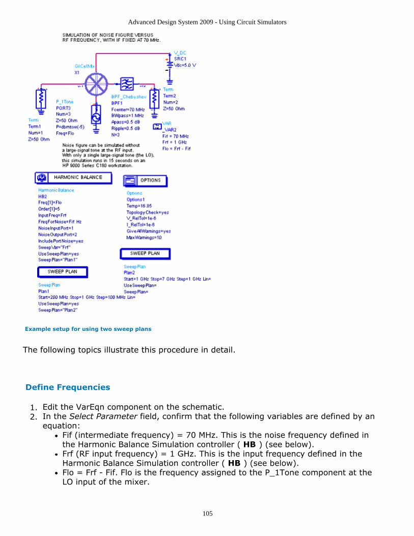
Advanced Design System 2009 - Using Circuit Simulators
105
Example setup for using two sweep plans
The following topics illustrate this procedure in detail.
Define Frequencies
Edit the VarEqn component on the schematic.1.In the Select Parameter field, confirm that the following variables are defined by an2.equation:
Fif (intermediate frequency) = 70 MHz. This is the noise frequency defined inthe Harmonic Balance Simulation controller ( HB ) (see below).Frf (RF input frequency) = 1 GHz. This is the input frequency defined in theHarmonic Balance Simulation controller ( HB ) (see below).Flo = Frf - Fif. Flo is the frequency assigned to the P_1Tone component at theLO input of the mixer.

Advanced Design System 2009 - Using Circuit Simulators
106
NoteThe simulator requires that all variables be initialized. Although a value of 0 MHz or 0 GHz issufficient to establish units for a local variable, leaving realistic units on the schematic allows ameaningful simulation to be conducted even when those variables are not swept.
These equations are written in the field on the right of the box, with Variable orEquation Entry Mode set to Name=Value.
Click Apply, then OK.3.
Establish Two Sweep Plans
From any simulation palette, select the SweepPlan controller and place two of these1.in the Schematic window.Edit the first SweepPlan (Plan1) as follows:2.
Sweep Type = LinearStart = 300 MHzStop = 1 GHzStep = 350 MHzSelect Next Sweep Plan, and enter Plan2 (to be established in the next step)in the field below the option.
Edit the second SweepPlan (Plan2) as follows:3.Sweep Type = LinearStart = 1 GHzStop = 7 GHzStep = 3 GHzBecause this is the last SweepPlan in this series, do not select Next SweepPlan or enter a plan name.
Define Sweep Frequencies and Sweep Plan in the Simulation Controller
Under the Sweep tab of the Harmonic Balance Simulation controller ( HB ), establish1.the following:
Parameter to sweep = Frf
NoteVariables entered into this field will appear in quotes on the schematic. If you enter a variabledirectly on the schematic (in this case, as the right-hand side of the SweepVar statement inthe DC controller), you must surround the variable with double quotes.
Sweep Type = LinearUse sweep plan is selected, and the entry in the field is Plan1. You can use thepulldown menu at the right of the field to select the name of a SweepPlancontroller.Other sweep parameter entries will be overridden by values in the SweepPlancontroller.Finally, because this is a noise analysis, also select Nonlinear noise to enablethe analysis.
Click Apply, then OK.2.

Advanced Design System 2009 - Using Circuit Simulators
107
Launch the Simulation and Display Data
Launch the simulation. The following are Rectangular and List plots of noise figure:1.
Additional Examples
An additional example of a swept-parameter simulation is found in the examples directory,in RFIC/Mixers_prj/networks. IMDLOSwp.dsn uses a ParamSweep controller to sweep LOpower in conjunction with harmonic balance simulation.
Recommendations and TipsThis section presents suggestions for using sweeps and improving the accuracy of results.
Ensuring that Sweep Results are Displayed Correctly
Parameter sweeps in the time domain are remarkable only in the way that they affect theadaptive time-step algorithm, which may have possible negative effects when results are displayed in the Data Display window. If the Transient simulator is allowed to use itsadaptive time-step algorithm and Max time step is not specified by the simulationcontroller, the simulator will probably produce results that have irregular data intervals.This does not matter when you are simulating only versus time and not sweeping – thatis, when you are attempting to produce only a single trace for each nodal waveform, not afamily of traces.
The potential difficulty arises when the Data Display server attempts to display a family oftraces, each having different numbers of trace points and irregular spacings. Simplystated, the data cannot be displayed. The Data Display server must have a rectangulararray of data. This means that all subtraces must have the same number of points, andthat the spacing between the points must be the same as that between the corresponding

Advanced Design System 2009 - Using Circuit Simulators
108
points in other subtraces. The spacing can be irregular, as long as the distribution ofspacing along the x-axis is the same for all traces. The only way to be sure that the DataDisplay server receives a neatly formatted, rectangular array of data is to specify a valuefor Max time step. This is especially true of Monte Carlo simulations, which are essentiallystatistical parameter sweeps.
Controlling the Amount of Data Sent to the Dataset
Time-domain simulations generally take more time and produce more nodal data than docomparable frequency-domain simulations. Hundreds (or even thousands) of time pointsmay be required to simulate the behavior of the circuit accurately. This makes it especiallyimportant to minimize the number of time points and swept parameter values. You cancontrol the amount and kind of data sent to the dataset using the Output tab of eachanalysis controller.
Using Sweeps in Monte Carlo Analysis
It is possible to use sweeps in Monte Carlo statistical analyses with the transientsimulator, to the extent that histograms can be generated. Yield percentage analyses arenot possible except through the following indirect method.
NoteMonte Carlo analyses are enabled through the use of the Yield and YieldOptim components in theOptim/Stat/Yield palette (under their Parameters tab, enable Random variables to dataset, and establishseed values as appropriate).
Yield percentages can be estimated if the pass/fail yield criterion can be expressed interms of node voltages and currents at individual time points.
Instead of plotting a histogram, plot the cumulative distribution function (CDF) using thecdf() operator and equations. The CDF increases monotonically from 0 to 1. Insert twomarkers onto the CDF trace at the limits of the pass/fail criterion. Then use the deltamarker mode to find the difference between them. The yield percentage is the differencebetween the two markers, multiplied by 100. For example, suppose the response of acircuit to a 1.0-V step with a 100-psec risetime is being plotted. The maximum risetimedesired from the circuit is 300 psec.
Ask for 100 Monte Carlo trials. Select the time point where the output voltage must be atleast 90% (perhaps t = 350 psec). Then plot the CDF multiplied by 100. Insert a markeron the 90% value and another on the maximum value, then examine the difference. Thisdifference is approximately the yield.
Monte Carlo statistical analyses can be regarded as a special type of parameter sweep inwhich the parameter values are assigned randomly, rather than as a succession ofascending values.

Advanced Design System 2009 - Using Circuit Simulators
109
SweepPlan Controller The options listed in the following table describe the SweepPlan controller's parameters.This controller sweeps a parameter which may be called by a ParamSweep controller or asimulator. It is unitless, as the parameter it sweeps can be any parameter. In the table,names used in netlists and schematics appear under Parameter Name.
Sweep Plan Options

Advanced Design System 2009 - Using Circuit Simulators
110
Setup DialogName
Parameter Name Description
SweepPlanInstance Name
Enter the name of the SweepPlan controller. The default isSwpPlan1.
Parameter Use this area in conjunction with the Add button to addStart, Stop, and Step parameters to the schematic. Use theCut button to remove a parameter set, and Paste to copyone that has been selected.
Sweep Type
Single point Pt Enables simulation at a single frequency point. Specify thedesired value in the Parameter field.
Linear Enables sweeping a range of values based on a linearincrement. Click the Start/Stop option to select start andstop values for the sweep, or Center/Span to set the centervalue and a span of the sweep.
Log Enables sweeping a range of values based on a logarithmicincrement. Click Start/Stop to set start and stop values forthe sweep, or Center/Span to select a center value and aspan of the sweep.
Start/StopStart, Stop,Step-size,Pts./decade,Num. of pts.
StartStopStepDecLin
Select the Start/Stop option to sweep based on start, stop,step-size or pts./decade, and number of points. Linearsweep uses Step-size; Log sweep uses Pts./decade.- Start-the start point of a sweep- Stop-the stop point of a sweep- Step-size-the increments at which the sweep is conducted- Pts./decade-number of points per decade- Num. of pts.-the number of points over which sweep isconducted
Center/SpanCenter, Span,Step-size,Pts./decade,Num. of pts.
CenterSpanStepDecLin
Select the Center/Span option to sweep based on centerand span, step-size or pts./decade, and number of points.Linear sweep uses Step-size; Log sweep uses Pts./decade.- Center-the center point of a sweep- Span-the span of a sweep- Step-size-the increments at which the sweep is conducted- Pts./decade-number of points per decade- Num. of pts.-the number of points over which sweep isconducted
Note: Changes to any of the Start, Stop, etc. fields causes the remaining fields to be recalculatedautomatically.
IncreasingOrder
Reverse=no Start and progress through sweep from lower to highervalues.
DecreasingOrder
Reverse=yes Start and progress through sweep from higher to lowervalues.
Next SweepPlan
UseSweepPlan=yesSweepPlan= Use this field to enter the name of the sweep plan(SweepPlan) to be performed after the current plan.
Parameter Sweep Controller This section describes the fields of the Parameter Sweep controller tabs. In the followingtables, names used in netlists and schematics appear under Parameter Name.

Advanced Design System 2009 - Using Circuit Simulators
111
Parameter Sweep Options
Setup DialogName
ParameterName
Description
ParamSweepInstance Name
Enter the name of the sweep controller. The default is Sweep1.
Parameter tosweep
SweepVar Use this area to select from a variety of sweep types and other parameters.In any parameter sweep, selecting a sweep start point as close as possible tothe convergence point and varying the parameter gradually shortenssimulation time. This yields better estimates for the next simulation, andachieves convergence more rapidly than if the parameter were changedabruptly.
Parameter sweep
Sweep Type
Single point Pt Enables simulation at a single frequency point. Specify the desired value inthe Parameter field.
Linear Enables sweeping a range of values based on a linear increment. Click theStart/Stop option to select start and stop values for the sweep, orCenter/Span to set the center value and a span of the sweep.
Log Enables sweeping a range of values based on a logarithmic increment. ClickStart/Stop to set start and stop values for the sweep, or Center/Span toselect a center value and a span of the sweep.
Start/StopStart, Stop,Step-size,Pts./decade,Num. of pts.
StartStopStepDecLin
Select the Start/Stop option to sweep based on start, stop, step-size orpts./decade, and number of points. Linear sweep uses Step-size; Log sweepuses Pts./decade.- Start-the start point of a sweep- Stop-the stop point of a sweep- Step-size-the increments at which the sweep is conducted- Pts./decade-number of points per decade- Num. of pts.-the number of points over which sweep is conducted
Center/SpanCenter, Span,Step-size,Pts./decade,Num. of pts.
CenterSpanStepDecLin
Select the Center/Span option to sweep based on center and span, step-sizeor pts./decade, and number of points. Linear sweep uses Step-size; Logsweep uses Pts./decade.- Center-the center point of a sweep- Span-the span of a sweep- Step-size-the increments at which the sweep is conducted- Pts./decade-number of points per decade- Num. of pts.-the number of points over which sweep is conducted
Note: Changes to any of the Start, Stop, etc. fields causes the remaining fields to be recalculatedautomatically.
Use sweep plan SweepPlan To use a sweep plan that you have defined and named, select this option andenter the name of the plan in the field.
Simulations Tab

Advanced Design System 2009 - Using Circuit Simulators
112
Setup DialogName
Parameter Name Description
ParamSweepInstance Name
Enter the name of the sweep controller. The default is Sweep1
Simulations toperform
SimInstanceName[n] Use this area to enter the name(s) of the simulation(s) you wish toperform. As an example, entering DC1, AC1, and HB3 in the setupdialog box causes the following to appear in the schematic: Simulation1="DC1", Simulation 2="AC1", and Simulation 3="HB3".The simulation controller instance name(s) entered should includedouble quotation marks ("name") on the schematic. The quotationmarks are inserted automatically when you enter a name using thedialog box. You must include the quotation marks if you enter namesdirectly on the schematic. If the quotation marks are missing, thesimulation will not work.Simulations will be performed in the sequence listed.
Display Tab
For information on the Display tab, which enables you to control the visibility of simulationparameters on the Schematic, see the topic Displaying Simulation Parameters on theSchematic (cktsim).

Advanced Design System 2009 - Using Circuit Simulators
113
Working with Data FilesData files are ASCII text representations of circuit responses based on various settings ofindependent variables. For instance the S-parameter response of an amplifier can becaptured against frequency and power variations in a .p2d data file. Some ADScomponents, such as the AmplifierP2D_Setup and AmplifierS2D_Setup help create datafiles. Other sources for data files are measurement instruments or other simulation toolswhich output circuit responses in text form. Thus data files enable you to take data fromsources outside of Advanced Design System or RF Design Environment and apply it toprojects within these design environments.
The common purpose of all the various applications which require the use of data files, isto generate the behavior of a specific component or a circuit based on simulated ormeasured data points. Thus, data files allow the transfer of realistic parameter values tosimple components and also enable the modeling of components with complex behaviorsuch as black box and gray box models. Some examples of the use of data files are:
Using S-parameters to define the behavior of a linear black-box componentrepresenting an attenuator, a filter, or a small-signal transistor. The S-parameters,which are saved in a file, are used in conjunction with a component like the S2P. Thispermits the creation of a realistic and customized 2-port network during an ADSsimulation.Storing sets of transistor model parameters in separate files, and accessing themautomatically through the course of a simulation to define the behavior of thetransistor.Defining the behavior of a complex nonlinear amplifier by using the gray-boxAmplifierS2D component and data saved in an S2D file. The small and large signal S-parameters as well as noise parameters contained within the file can be used todefine the behavior of the amplifier during a simulation.
Besides data-file driven components, there are other user-defined models such as usingSDDs, FDDs, equation-based components, or the Model Builder which are discussedelsewhere. This section focuses on how to use the various types of data files to define thebehavior of components and circuits in addition to providing a comprehensiveunderstanding of the classification and formats associated with the various types of datafiles used by various components.
A data file is simply data in an ASCII text file, but there are several formats to choosefrom depending on the application. When determining the type of data file to chooseplease note:
The format you choose may depend on the type of data you have and where youwant to use the data. The table below lists supported file formats and examples ofwhere they are used.The DataAccessComponent may be used to access the data from any data fileregardless of format and to use it with any component that accepts file-basedparameters. In this case, you need to make sure there is a logical relationshipbetween the data and how you intend to use it. For more information, see Using DataFiles, Datasets, and Data Access Components.

Advanced Design System 2009 - Using Circuit Simulators
114
Supported Data FormatsThe following table lists the supported data formats with a brief description and areference to detailed information:
Available File Format Types
Format Description Usage Details
Touchstone Format
SnP †,††
(.snp)Small signal S, H, Y, Z, or G-parameters. May also include optionalnoise data (2 port data only). Wheren is the number of ports from 1 to99.
n-port S-parameter file (S n P)components in the Data ItemsLibrary.
Touchstone SnPFormat
Impulse(.imp)
ADS Impulse (.imp) files store multi-port impulse responses of linear N-ports. These files are the time-domain analog of the frequency-domain Touchstone format.
Data output from theImpulseWriter (Impulse ResponseFile Writer controller).
ADS Impulse FileFormat
MDIF Formats
Discrete(.dscr)
Discrete (indexed) tabular andpossibly statistical density data.
Components that accept file-basedparameters, link via the DAC.
Discrete Format
Model MDIF Nonlinear model parameters. EE_BJT2_Model, JFET_Model, etc. Model MDIF Files
PDF ‡‡‡
(.pdf)User defined, piece-wise linearprobability density function data forarbitrary distributions that are notcorrelated.
With expressions in the Statisticstab.
PDF Format
S2PMDIF(.s2p)
Multi-dimensional 2-port, S, Y, Z, H,G signal and optional 2-port noiseparameter (Fmin, Gopt, Rn) data.
With S2PMDIF, DAC, andcomponents represented by blackbox statistical characterization.
S2PMDIF Format
P2D †,††
(.p2d)Large-signal, power-dependent, 2-port S, H, Y, Z, or G -parameters.
AmplifierP2D in the System - Amps& Mixers library.
P2D Format
S2D †,††
(.s2d)2-port S, H, Y, Z, or G-parameterswith forward gain compression andoptional noise and intermodulationdata.
Amplifier2 and AmpSingleCarrier inthe System-Amps & Mixers library,AmplifierS2D in the System-DataModels library.
S2D Format
IMT ††
(.imt)Intermodulation product table ofmixer intermodulation productsbetween the LO and signal thatrelates the mixer IM output level tosignal input level.
MixerIMT in the System - Amps &Mixers library. MixerIMT Data inthe System-Data Models library.
IMT Format
SPW ††
(.ascsig text) (.sigbinary )
Time-domain voltage data file inCadence Alta Group SPW text andbinary formats.
TimeFile item in Timed Sourcesand OutFile item in the Sinkslibrary.
SPW Format
TIM ††
(.tim)Time-domain data. TimeFile item in Timed Sources
and OutFile item in Sinks library.TIM Format

Advanced Design System 2009 - Using Circuit Simulators
115
SDF ††,†††
(.sdf)Time-domain voltage data file in89600 file format.
TimeFile item in Timed Sourcesand OutFile item in Sinks library.
See softwaredocumentation forthe Agilent 89600.
GCOMP †† Gain compression data Amplifier and Mixer items in theSystem - Amps & Mixers library.
UnderstandingGCOMP Data
GenericMDIF (.mdif)
Generalized multi-dimensional tablesunifying other MDIF formats. Use inplace of any specific MDIF.
AmplifierS2D, AmplifierP2D, or anyother MDIF example listed above.Link via the DAC.
Generic MDIF
CITIfile Format
CITIfile ††† A general data format supported bynetwork analyzers. Capable of storingmultiple packages of multi-dimensional data.
n-port S-parameter file (S n P)components in the Data ItemsLibrary.
CITIfile Data Format
Agilent IC-CAP Formats
DUT, MDL,SET ‡,‡‡
Device under test (DUT), model(MDL), and setup (SET) files from theAgilent IC-CAP program. These filescan contain Measured, Simulated,and/or Transformed data.
Once the data is read into adataset, it can be used with anycomponent (for example, aVtDataset source) that can readdata from a dataset.
See Agilent IC-CAPdocumentation.
† When writing data from a dataset to a file, the variable names are limited to S,H,Y,Z or G, for example,S[1,1], S[1,2], G[1,1], G[1,2]. The variable name is used to determine the type of data.†† The first set of data in the dataset that matches the data type (name) will be output. It is not possible toarbitrarily select which data will be output.††† There are some specific problems with the current version in writing and/or reading this data format. Onthe Agilent EEsof web site, refer to the Release Notes in Product Documentation and to Technical Support formore information and workarounds (www.agilent.com/find/eesof).‡ The Data File Tool can only read IC-CAP data.‡‡ Only simple, scaled expressions with numbers or variables and one operator (either +, -, *, or /) aresupported for start, stop, step, and number of points parameters, for example, start= 1 GHZ orstop=icmax/10.‡‡‡ This format is not yet fully supported.The COD, FIR, LAS, and SPE formats were obsolete when ADS 1.0 was introduced and are not used by theapplication. The LIST2 and T2D formats are also obsolete.
For information about a particular component, refer to the documentation for Analog/RF orSignal Processing components, or click Help when editing component parameters.
Making a Data FileYou can create a data file using these methods:
Manually type the data into a text file using any text editor, being sure to follow theformatting guidelines for the type of data file that you want.Use the Data File Tool. The Data File Tool enables you to transfer data betweendatasets and files that are in the following file formats: Touchstone, Measurementdata interchange format (MDIF), CITIfile, and IC-CAP. For learn about the Data FileTool, see Reading and Writing Data Files.Perform a P2D controller-based simulation using AmplifierP2D_Setup orAmplifierS2D_Setup. The results of these simulations are saved to files in P2D andS2D formats respectively, which can then be used with the AmplifierP2D orAmplifierS2D. For more information on the P2D controller itself, see P2D Simulation

Advanced Design System 2009 - Using Circuit Simulators
116
(cktsimp2d).
Saving a Data FileWhen saving a data file, save it as an ASCII text file.
A data file does not require a particular extension, but you may want to use theextension recommended for each format for identification purposes. These extensionsare given in the details describing each format. If you choose a different extension,you must provide this information to the component you intend to use through theFile parameter of the component.
You can save the data file:
In the project where it is used under the <prj>/data directory. This is the defaultlocation if no path is provided to the component using the file.Any location, if you provide the full file path to the component. You provide thisinformation using the File parameter of the component.
For more information about the File parameter, place the component of interest on aschematic, double-click to edit it, and click the Help button at the bottom of the dialogbox.
Using Data Files, Datasets, and Data AccessComponentsBoth data files and datasets can contain data that you want to use with a component. Youcan use either one, depending on your situation:
You may want the S-parameters from a simulated design. In this case, use thedataset and a DAC to link the data to the component you want to use.You may have S-parameter specifications from a component sheet. In this case, typethem into a data file.
You also want to consider the method of linking your data with the component of interest:
You have a data file, such as an .s2d, and you want to use it with a component thatcan read such a file, such as the AmplifierS2D. No DAC is needed.You have a dataset or data file, but the component you want to use doesn't read thedata directly. Use a DataAccessComponent to link the data file and component. Thecomponent you choose must have the file-based option under the Parameter EntryMode or the parameter AllParams. For example, the BJTM1 model has the parameterAllParams; the R component has the Parameter Entry Mode. For instructions on howto use a DAC, see DataAccessComponent (Data Access Component) (ccsim) orSchematic Capture and Layout (usrguide).

Advanced Design System 2009 - Using Circuit Simulators
117
Reading and Writing Data Files Use the Data File Tool to import and export data between datasets and text files that arein the following file formats:
TouchstoneMeasurement data interchange format (MDIF)CITIfileIC-CAP
You can transfer data from a file into a dataset, or vice versa. One application is totransfer data from a dataset to an MDIF file, for use with a specific type of component. Forexample, a file in P2D format (P2D is one of several MDIF formats) containing S-parameters can then be used by the P2D amplifier. Using the Data File Tool, you can writeS-parameters from a dataset to a file in P2D format. Another application is reading AgilentIC-CAP data into a dataset to be used in conjunction with a component, such as a source,that can read data from a dataset.
See the table above in Supported Data Formats for a list of the available file types, adescription of the file contents, and the component that uses the data. Be sure to reviewthe notes at the end of the table. The details about each file format are described later inthis topic.
Starting and Exiting the Data File Tool
You can start the Data File Tool from a Schematic window or a Data Display Window.
From a Schematic window, choose Tools > Data File Tool. Or, click the Data FileTool icon.
From a Data Display window, choose Tools > Data File Tool. Or, click the Data FileTool icon.
To exit the Data File Tool, choose File > Exit from the menu bar.
Parts of the Data File Tool
The following illustration shows the default appearance of the Data File Tool user interfacefor a UNIX-based system when the Data File Tool is started.
The layout of the interface and names of the various elements vary with the task being

Advanced Design System 2009 - Using Circuit Simulators
118
performed (read or write) and can also vary with the file format selected. Examples of thisvariation in the appearance of the Data File Tool user interface is shown in the twofollowing figures.

Advanced Design System 2009 - Using Circuit Simulators
119
Data File Tool in read mode
Data File Tool in write mode
Advanced Design System 2009 - Using Circuit Simulators
120
These are the more frequently used elements of the interface:
The Menu bar displays the menus that are available in the Data File Tool window.The Dataset field lists the datasets in the current project. The selected dataset or thename of a new dataset is displayed in the Dataset name field.
Reading a File
To read the contents of a file into a dataset:
From an open Data File Tool window, click Read data file into dataset.1.Under File format to read, select one of the following file formats:2.
TouchstoneMDIFCitifileICCAP
For the MDIF format, choose the appropriate sub-format from MDIF sub type.3.Under Input file name, type in the file name if the file is in the project. If it is not,4.click Browse to locate and select the file.The data from the selected file will be written to a dataset. Enter a name in the5.Dataset name field or select from the existing datasets in the Datasets list. If youchoose a dataset from the list, any data that is already stored in the dataset will notbe saved and will be overwritten with new data.Click Read File to send the file contents to the dataset.6.
NoteThe source file must not use any ADS reserved variables or non-ASCII characters. Use of such a filecan produce misleading results.
Writing to a File
To write data to a file:
From an open Data File Tool window, click Write data file from dataset.1.Under File format to write, select one of the following file formats:2.
TouchstoneMDIFCitifile
For the Touchstone and MDIF formats, choose the appropriate sub-format from3.Touchstone data type, or MDIF sub type.Under Output file name, type in the file name you want to write to. It will be saved4.in the project directory. If you want to save the file in a different location, clickBrowse to select a location.Under Complex data format, select the complex data format to be used in the file.5.For Touchstone and MDIF files, under Frequency units, select the frequency units to6.

Advanced Design System 2009 - Using Circuit Simulators
121
be used in the file.Under Data notation format, select the data notation format to be used in the file.7.Under Max resolution, select the maximum resolution to be used in the file.8.The source of the data can be any project dataset. It should contain data matching9.the file format selected. Select an existing dataset from the Datasets list. Click ViewDataset to view the contents of the selected dataset.Click Write to File to send the data to the file.10.
NoteIf a dataset has just been created by reading a file, it might be necessary to click Update DatasetList to see it appear in the list.
ExamplesYou can find designs that use different data files in the Examples directory underData_comp_prj and DataAccess_prj.
Instructions for using a particular type of file with a component that is designed to readthe file (like an . snp file and SnP component) can be found in the remaining referencesections.
Touchstone SnP Format These files contain small-signal G-, H-, S-, Y-, or Z-network parameters described byfrequency-dependent linear network parameters for 1- to 99-port components. The 2-portcomponent files can also contain frequency-dependent noise parameters. This data fileformat is also known as Touchstone format.
An .snp file can be used with an SnP component to model the behavior of a linear modelusing S-parameters. The file contains the S-parameters, the component is placed withinthe schematic.
This section describes:
Choosing an .snp file for use with an SnP componentAn overview of the SnP fileThe basic SnP formatAdding noise to a 2-port Snp fileThe basic SnP format applied to G-, H-, S-, Y-, and Z-parameters, plus examples ofeach
Linking an .snp File to an SnP Component
To link a file to the component:
Add an SnP component to your schematic. It can be found in the Data Items library.1.

Advanced Design System 2009 - Using Circuit Simulators
122
Select the File parameter. Ensure that the Parameter Entry Mode is set to Network2.Parameter File Name .In the File Name field, enter the name of the file you want to use:3.
You can type the name directly in the field.Click Data files list to locate a file in the current project (or any files locatedbased on the setting of the DATAFILES variable in de_sim.cfg).Click Browse to locate a file outside the current project.Click Copy template to select an example file that you can customize.
After you select a file, click Edit if you want to view the file or change its contents.4.
For instructions on how to set the remaining parameters, click Help in the opencomponent dialog box.
Overview
SnP data files are ASCII text files in which data appears line by line, one line per datapoint, in increasing order of frequency. Each line of data consists of a frequency value andone or more pairs of values for the magnitude and phase of each S-parameter at thatfrequency. Values are separated by one or more spaces, tabs or commands. Commentsare preceded by an exclamation mark (!). Comments can appear on separate lines, orafter the data on any line or lines. Extra spaces are ignored. Recommendations forfilenames are:
1-port: filename.s1p
2-port: filename.s2p
Up to 99 ports can be defined.
You can specify the following parameters in an .snp file:
S = Scattering parameters
Y = Admittance parameters
Z = Impedance parameters
H = Hybrid-h parameters
G = Hybrid-g parameters
NoteThe mismatched port impedance is not supported by the ADS simulator. If a Touchstone file has theinput/output mismatch information in the header, it is ignored by the DAC and the SnP components, and adefault matching 50 ohm port impedance is used.
The following sections discuss the content and format of network parameter files as inputfor circuit analysis.
Basic SnP File Format

Advanced Design System 2009 - Using Circuit Simulators
123
The following example shows the general format for component data files. It consists of:
An option lineData linesComments
The Option Line
The option line, specifying the frequency units and the normalizing impedance, precedesthe data lines.# (freq_units parameter format R n)<data line>...<data line>where:
# = The delimiter that tells the program you are specifying these parameters
freq_units = Sets the units. Options are GHz, MHz, KHz, or Hz.
parameter = Sets the desired parameter. Options are S, Y, Z, G, or H.
format = The format desired. Options are MA, DB, or RI.
R n = The reference resistance in ohms, where n is a positive number of ohms; which is the realimpedance to which the parameters are normalized.
In summary, the option line should read:
For .s1p files: # [HZ/KHZ/MHZ/GHZ] [S/Y/Z] [MA/DB/RI] [Rn]
For .s2p files: # [HZ/KHZ/MHZ/GHZ] [S/Y/Z/G/H] [MA/DB/RI] [Rn]
For .s3p/.s4pfiles:
# [HZ/KHZ/MHZ/GHZ] [S] [MA/DB/RI] [Rn]
where square brackets [...] indicate optional information; .../.../.../ indicates that youselect one of the choices; and, n is replaced by a positive number.
Default Option Line
The default option line for component data files is:# GHZ S MA R 50
Option Line Examples
Frequency in GHz, S-parameters in real-imaginary format, normalized 100 ohms:

Advanced Design System 2009 - Using Circuit Simulators
124
# GHz S RI R 100
Frequency in KHz, Y-parameters in real-imaginary format, normalized 100 ohms:# KHz Y RI R 100
Frequency in Hz, Z-parameters in magnitude-degree format, normalized to 1 ohm:# Hz Z MA R 1
Frequency in KHz, H-parameters in real-imaginary format normalized to 1 ohm:# KHz H RI R 1
Frequency in Hz, G-parameters in magnitude-degree, format normalized to 1 ohm:# Hz G MA R 1
Data Lines
Data lines contain the data of interest. A special format is used for 2-port data files whereall of the network parameter data for a single frequency is listed on one line. The order ofthe network parameters is:
N11, N21, N12, N22
For 3-port or higher data files, the network parameters appear in the file in a matrix form,each row starting on a separate line. A maximum of four network parameters (with 2 realnumbers for each) appear on any line. The remaining network parameters are continuedon as many additional lines as are needed.
The following sections describe the data-line format for single and multi-port components.
Data-line Formats
When you type the data below the option line, the columns need not line up precisely likethose shown. The syntax for entering data is as follows:
1-port ComponentMagnitude-Angle format:
(Columns: f Mag Ang)
f |S11|
2-port ComponentMagnitude-Angle format:
f |S11| <S11 |S21| <S21 |S12| <S12 |S22|
Real-Imaginary format:

Advanced Design System 2009 - Using Circuit Simulators
125
f Re{S11} Im{S11} Re{S21} Im{S21} Re{S12} Im{S12} Re{S22} Im{S22}
dB-Angle format:f 20log10|x11| <x11 20log10|x21| <x21 20log10|x12| <x12 20log10|x22|
where
x = S/Y/Z/H/G
f = Frequency
3-port ComponentMagnitude-Angle format:
( Columns : f Mag Ang Mag Ang Mag Ang)
f |S11| <S11 |S12| <S12 |S13| <S13
|S21| <S21 |S22| <S22 |S23| <S23
|S31| <S31 |S32| <S32 |S33| <S33
4-port ComponentMagnitude-Angle format:
( Columns : f Mag Ang Mag Ang Mag Ang Mag Ang)
f |S11| <S11 |S12| <S12 |S13| <S13 |S14| <S14
|S21| <S21 |S22| <S22 |S23| <S23 |S24| <S24
|S31| <S31 |S32| <S32 |S33| <S33 |S34| <S34
|S41| <S41 |S42| <S42 |S43| <S43 |S44| <S44
where:
f = Frequency
Mag = Magnitude of S-parameter Sij
Ang = Angle of S-parameter Sij
Adding Comments to Data Files
You can document your data files by preceding a comment with the exclamation mark (!)on any line. A comment can be the only entry on a line or can follow the data on any line.
Adding Noise Parameters to an SnP File
Noise parameters can be included in SnP 2-port data files. Noise data can follow G-, H-,S-, Y-, or Z-parameters described for each frequency. The x values are data.

Advanced Design System 2009 - Using Circuit Simulators
126
Each line of a noise parameter has the following five entries:
x1 x2 x3 x4 x5
where:
x1 = Frequency in units. The first point of noise data must have a frequency less than the frequency of thelast S-parameter frequency
x2 = Minimum noise figure in dB
x3 = Source reflection coefficient to realize minimum noise figure (MA)
x4 = Phase in degrees of the reflection coefficient (MA)
x5 = Normalized effective noise resistance. The system simulator requires this parameter to meet physicalrequirements. If the user-supplied x5 value is less than allowed for this requirement, then the systemsimulator will force this x5 value to the lowest physical limit.
Sopt noise data in an SnP file must be expressed in a Magnitude/Angle (MA) format. Thesimulator assumes that the Sopt noise data in an SnP file is specified in a MA format. Thisis the only supported format for Sopt data in an SnP file. The complex format typespecified in the format line does not apply to the Sopt data specified in the Noise block.
The data file reader cannot determine if the numbers representing the Sopt data in theSnP data file are expressed in MA format and not in dB or Real/Imag formats. It reads inwhatever numbers appear on the data line and processes them as if they are MA, withoutissuing an error or warning message. If the Sopt data in the SnP data file is expressed in aformat other than MA, this can produce simulation data that look incorrect.
NoteThe frequencies for noise parameters and network parameters need not match. The only requirement isthat the lowest noise-parameter frequency be less than or equal to the highest network-parameterfrequency. This allows the file processor to determine where network parameters end and noiseparameters begin.
The source reflection coefficient and effective noise resistance are normalized to the sameresistance as specified for the network parameters.
Example File Containing Noise Data
This is an example of a data file with noise data:
! NEC710
# GHZ S MA R 50
2 .95 -26 3.57 157 .04 76 .66 -14
22 .60 -144 1.30 40 .14 40 .56 -85
! NOISE PARAMETERS
4 .7 .64 69 .38
18 2.7 .46 -33 .40

Advanced Design System 2009 - Using Circuit Simulators
127
Applying the SnP Format, and Examples
In this section are formatting references and examples for:
G-parameter filesH-parameter filesS-parameter filesY- and Z-parameter files
Guidelines
The optimum source reflection coefficient and the normalized effective noiseresistance are assumed to be with respect to the normalizing resistance value(appearing after the R keyword) on the header line.The frequencies for noise parameters and G-, H-, S-, Y-, or Z-parameters (networkparameters) do not have to match. The only requirement is that the lowest noiseparameter frequency be less than or equal to the highest network parameterfrequency. This allows the file processor to determine where G-, H-, S-, Y-, or Z-parameters end and noise parameters begin.
G-Parameter Files
G-parameter files (Hybrid-g parameters) use MA or RI format. They are strictly 2-portfiles. G-parameter measurements are:
G11 input admittance (port 2 open)
G22 output impedance (port 1 shorted)
G21 forward voltage gain (port 2 open)
G12 reverse current gain (port 1 shorted)
G-Parameter MA and RI File Formats
# frequency_unit G MA R impedance
freq magG11 angG11 magG21 angG21 magG12 angG12 magG22 angG22
# frequency_unit G RI R impedance
freq reG11 imG11 reG21 imG21 reG12 mG12 reG22 imG22
G-Parameter File Example
! symbol freq-unit parameter-type data-format keyword impedance-ohms
# KHZ G MA R 1

Advanced Design System 2009 - Using Circuit Simulators
128
! freq magG11 angG11 magG21 angG21 magG12 angG12 magG22 angG22
2 .95 -26 3.57 157 .04 76 .66 -14
3 .93 -40 3.53 147 .05 69 .65 -20
4 .89 -52 3.23 136 .06 62 .63 -26
H-Parameter Files
H-parameter files (Hybrid-h parameters) use MA or RI format. They are strictly 2-portfiles. H-parameter measurements are:
H11 input impedance (port 2 shorted)
H22 output admittance (port 1 open)
H21 forward current gain (port 2shorted)
H12 reverse voltage gain (port 1 open)
H-Parameter File Example
! symbol freq-unit parameter-type data-format keyword impedance-ohms
# KHZ H MA R 1
! freq magH11 angH11 magH21 angH21 magH12 angH12 magH22 angH22
2 .95 -26 3.57 157 .04 76 .66 -14
3 .93 -40 3.53 147 .05 69 .65 -20
4 .89 -52 3.23 136 .06 62 .63 -26
S-Parameter Files
S-parameter files (scattering parameters) can have MA, RI, or DB format for files with 1 to99 ports.
S-Parameter 1-Port MA, RI, and DB File Formats
# frequency_unit S MA R impedance
freq magS11 angS11
# frequency_unit S RI R impedance
freq reS11 imS11
# frequency_unit S DB R impedance
freq dbS11 angS11
S-Parameter 2-Port MA, RI, and DB File Formats

Advanced Design System 2009 - Using Circuit Simulators
129
# frequency_unit S MA R impedance
freq magS11 angS11 magS21 angS21 magS12 angS12 magS22 angS22
# frequency_unit S RI R impedance
freq reS11 imS11 reS21 imS21 reS12 imS12 reS22 imS22
# frequency_unit S DB R impedance
freq dbS11 angS11 dbS21 angS21 dbS12 angS12 dbS22 angS22
S-Parameter 3-Port MA, RI, and DB File Formats
# frequency_unit S MA R impedance
freq magS11 angS11 magS12 angS12 magS13 angS13 ! 1st row
magS21 angS21 magS22 angS22 magS23 angS23 ! 2nd row
magS31 angS31 magS32 angS32 magS33 angS33 ! 3rd row
# frequency_unit S RI R impedance
freq reS11 imS11 reS12 imS12 reS13 imS13 ! 1st row
reS21 imS21 reS22 imS22 reS23 imS23 ! 2nd row
reS31 imS31 reS32 imS32 reS33 imS33 ! 3rd row
# frequency_unit S DB R impedance
freq dbS11 angS11 dbS12 angS12 dbS13 angS13 ! 1st row
dbS21 angS21 dbS22 angS22 dbS23 angS23 ! 2nd row
dbS31 angS31 dbS32 angS32 dbS33 angS33 ! 3rd row
S-Parameter 4-Port MA, RI, and DB File Formats
# frequency_unit S MA R impedance
! 1st row
freq magS11 angS11 magS12 angS12 magS13 angS13 magS14 angS14
magS21 angS21 magS22 angS22 magS23 angS23 magS24 angS24 ! 2nd row
magS31 angS31 magS32 angS32 magS33 angS33 magS34 angS34 ! 3rd row
magS41 angS41 magS42 angS42 magS43 angS43 magS44 angS44 ! 4th row
# frequency_unit S RI R impedance
freq reS11 imS11 reS12 imS12 reS13 imS13 reS14 imS14 ! 1st row
reS21 imS21 reS22 imS22 reS23 imS23 reS24 imS24 ! 2nd row
reS31 imS31 reS32 imS32 reS33 imS33 reS34 imS34 ! 3rd row
reS41 imS41 reS42 imS42 reS43 imS43 reS44 imS44 ! 4th row
# frequency_unit S DB R impedance
freq dbS11 angS11 dbS12 angS12 dbS13 angS13 dbS14 angS14 ! 1st row
dbS21 angS21 dbS22 angS22 dbS23 angS23 dbS24 angS24 ! 2nd row
dbS31 angS31 dbS32 angS32 dbS33 angS33 dbS34 angS34 ! 3rd row
dbS41 angS41 dbS42 angS42 dbS43 angS43 dbS44 angS44 ! 4th row
S-Parameter 1-Port File Example
! symbol freq-unit parameter-type data-format keyword impedance-ohms
# MHZ S MA R 50
! freq magS11 angS11 (commented header line)
2.000 0.894 -12.136
3.000 0.893 -18.179

Advanced Design System 2009 - Using Circuit Simulators
130
4.000 0.891 -24.193
S-Parameter 5- to 99-Port File Formats
These file formats appear in a matrix form similar to the 3- and 4-port files, except thatonly four S-parameters (with 2 real numbers for each) can appear on a given line.Therefore, the remaining S-parameters in that row of the S-matrix continue on the nextline of the file.
Each row of the S-matrix must begin on a new line of the file. The first line of the first rowof the S-matrix begins with the frequency value.
S-Parameter 10-Port File Example (at One Frequency)
# frequency_unit S MA R impedance
freq magS11 angS11 magS12 angS12 magS13 angS13 magS14 angS14 ! 1st row
magS15 angS15 magS16 angS16 magS17 angS17 magS18 angS18
magS19 angS19 magS1,10 angS1,10
magS21 angS21 magS22 angS22 magS23 angS23 magS24 angS24 ! 2nd row
magS25 angS25 magS26 angS26 magS27 angS27 magS28 angS28
magS29 angS29 magS2,10 angS2,10
magS31 angS31 magS32 angS32 magS33 angS33 magS34 angS34 ! 3rd row
magS35 angS35 magS36 angS36 magS37 angS37 magS38 angS38
magS39 angS39 magS3,10 angS3,10
magS41 angS41 magS42 angS42 magS43 angS43 magS44 angS44 ! 4th row
magS45 angS45 magS46 angS46 magS47 angS47 magS48 angS48
magS49 angS49 magS4,10 angS4,10
magS51 angS51 magS52 angS52 magS53 angS53 magS54 angS54 ! 5th row
magS55 angS55 magS56 angS56 magS57 angS57 magS58 angS58
magS59 angS59 magS5,10 angS5,10
magS61 angS61 magS62 angS62 magS63 angS63 magS64 angS64 ! 6th row
magS65 angS65 magS66 angS66 magS67 angS67 magS68 angS68
magS69 angS69 magS6,10 angS6,10
magS71 angS71 magS72 angS72 magS73 angS73 magS74 angS74 ! 7th row
magS75 angS75 magS76 angS76 magS77 angS77 magS78 angS78
magS79 angS79 magS7,10 angS7,10
magS81 angS81 magS82 angS82 magS83 angS83 magS84 angS84 ! 8th row
magS85 angS85 magS86 angS86 magS87 angS87 magS88 angS88
magS89 angS89 magS8,10 angS8,10
magS91 angS91 magS92 angS92 magS93 angS93 magS94 angS94 ! 9th row
magS95 angS95 magS96 angS96 magS97 angS97 magS98 angS98
magS99 angS99 magS9,10 angS9,10
!10th row
magS10,1 angS10,1 magS10,2 angS10,2 magS10,3 angS10,3 magS10,4 angS10,4
magS10,5 angS10,5 magS10,6 angS10,6 magS10,7 angS10,7 magS10,8 angS10,8
magS10,9 angS10,9 magS10,10 angS10,10
Linear 1-Port (.s1p) File Example

Advanced Design System 2009 - Using Circuit Simulators
131
# GHZ S RI R 50.0
1.00000000 0.9488 -0.2017
1.50000000 0.9077 -0.3125
2.00000000 0.8539 -0.4165
2.50000000 0.7884 -0.5120
3.00000000 0.7124 -0.5978
3.50000000 0.6321 -0.6546
4.00000000 0.5479 -0.7013
4.50000000 0.4701 -0.7380
5.00000000 0.3904 -0.7663
5.50000000 0.3302 -0.7778
6.00000000 0.2702 -0.7848
6.50000000 0.2041 -0.7890
7.00000000 0.1389 -0.7878
7.50000000 0.0894 -0.7849
8.00000000 0.0408 -0.7789
8.50000000 0.0134 -0.7649
9.50000000 0.0654 -0.7471
9.00000000 0.1094 -0.7319
10.0000000 0.1518 -0.7140
Linear 2-Port (.s2p) File Example
# GHZ S RI R 50.0
1.0000 0.3926 -0.1211 -0.0003 -0.0021 -0.0003 -0.0021 0.3926 -0.1211
2.0000 0.3517 -0.3054 -0.0096 -0.0298 -0.0096 -0.0298 0.3517 -0.3054
10.000 0.3419 0.3336 -0.0134 0.0379 -0.0134 0.0379 0.3419 0.3336
!Noise params
1.0000 2.0000 -0.1211 -0.0003 .4
2.0000 2.5000 -0.3054 -0.0096 .45
3.0000 3.0000 -0.6916 -0.6933 .5
4.0000 3.5000 -0.3756 0.4617 .55
5.0000 4.0000 0.3880 0.6848 .6
6.0000 4.5000 0.0343 0.0383 .65
7.0000 5.0000 0.6916 0.6933 .7
8.0000 5.5000 0.5659 0.1000 .75
9.0000 6.0000 0.4145 0.0307 .8
10.0000 6.5000 0.3336 0.0134 .85
Linear 3-Port (.s3p) File Example
# GHZ S MA R 50.0
! POWER DIVIDER, 3-PORT
5.00000 0.24254 136.711 0.68599 -43.3139 0.68599 -43.3139
0.68599 -43.3139 0.08081 66.1846 0.28009 -59.1165
0.68599 -43.3139 0.28009 -59.1165 0.08081 66.1846
6.00000 0.20347 127.652 0.69232 -52.3816 0.69232 -52.3816
0.69232 -52.3816 0.05057 52.0604 0.22159 -65.1817
0.69232 -52.3816 0.22159 -65.1817 0.05057 52.0604
7.00000 0.15848 118.436 0.69817 -61.6117 0.69817 -61.6117
0.69817 -61.6117 0.02804 38.6500 0.16581 -71.2358
0.69817 -61.6117 0.16581 -71.2358 0.02804 38.6500

Advanced Design System 2009 - Using Circuit Simulators
132
Linear 4-Port (.s4p) File Example
# GHZ S MA R 50
5.00000 0.60262 161.240 0.40611 -42.2029 0.42918 -66.5876 0.53640 -79.3473
0.40611 -42.2029 0.60262 161.240 0.53640 -79.3473 0.42918 -66.5876
0.42918 -66.5876 0.53640 -79.3473 0.60262 161.240 0.40611 -42.2029
0.53640 -79.3473 0.42918 -66.5876 0.40611 -42.2029 0.60262 161.240
6.00000 0.57701 150.379 0.40942 -44.3428 0.41011 -81.2449 0.57554 -95.7731
0.40942 -44.3428 0.57701 150.379 0.57554 -95.7731 0.41011 -81.2449
0.41011 -81.2449 0.57554 -95.7731 0.57701 150.379 0.40942 -44.3428
0.57554 -95.7731 0.41011 -81.2449 0.40942 -44.3428 0.57701 150.379
7.00000 0.50641 136.693 0.45378 -46.4151 0.37845 -99.0918 0.62802 -114.196
0.45378 -46.4151 0.50641 136.693 0.62802 -114.196 0.37845 -99.0918
0.37845 -99.0918 0.62802 -114.196 0.50641 136.693 0.45378 -46.4151
0.62802 -114.196 0.37845 -99.0918 0.45378 -46.4151 0.50641 136.693
Y- and Z-Parameter Files
Immittance parameters are specified in MA or RI format, where the # line has Y foradmittance and Z for impedance. Both are normalized to the reference resistance.
Y- (Z-) Parameter 1-Port MA and RI File Formats
# frequency_unit Y MA R impedance
freq magY11 angY11
# frequency_unit Y RI R impedance
freq reY11 imY11
Y- (Z-) Parameter 2-Port MA and RI File Formats
# frequency_unit Y MA R impedance
freq magY11 angY11 magY21 angY21 magY12 angY12 magY22 angY22
# frequency_unit Y RI R impedance
freq reY11 imY11 reY21 imY21 reY12 imY12 reY22 imY22
Y- (Z-) Parameter 3-Port MA and RI File Formats
freq magY11 angY11 magY12 angY12 magY13 angY13 ! 1st row
magY21 angY21 magY22 angY22 magY23 angY23 ! 2nd row
magY31 angY31 magY32 angY32 magY33 angY33 ! 3rd row
# frequency_unit Y RI R impedance
freq reY11 imY11 reY12 imY12 reY13 imY13 ! 1st row

Advanced Design System 2009 - Using Circuit Simulators
133
reY21 imY21 reY22 imY22 reY23 imY23 ! 2nd row
reY31 imY31 reY32 imY32 reY33 imY33 ! 3rd row
Y- (Z-) Parameter 4-Port MA and RI File Formats
# frequency_unit Y MA R impedance
freq magY11 angY11 magY12 angY12 magY13 angY13 magY14 angY14 ! 1st row
magY21 angY21 magY22 angY22 magY23 angY23 magY24 angY24 ! 2nd row
magY31 angY31 magY32 angY32 magY33 angY33 magY34 angY34 ! 3rd row
magY41 angY41 magY42 angY42 magY43 angY43 magY44 angY44 ! 4th row
# frequency_unit Y RI R impedance
freq reY11 imY11 reY12 imY12 reY13 imY13 reY14 imY14 ! 1st row
reY21 imY21 reY22 imY22 reY23 imY23 reY24 imY24 ! 2nd row
reY31 imY31 reY32 imY32 reY33 imY33 reY34 imY34 ! 3rd row
reY41 imY41 reY42 imY42 reY43 imY43 reY44 imY44 ! 4th row
Y- (Z-) Parameter 3-Port File Example
! symbol freq-unit parameter-type data-format keyword impedance-ohms
# GHz Y MA R 1
!freq magY11 angY11 magY12 angY12 magY13 angY13 ! 1st line
! magY21 angY21 magY22 angY22 magY23 angY23 ! 2nd line
! magY31 angY31 magY32 angY32 magY33 angY33 ! 3rd line
4 0.008 83.122 8.5e-04 -86.740 0.007 -98.037
0.046 -12.740 0.005 36.580 0.049 171.554
0.046 177.588 0.004 -152.638 0.050 0.134
8 0.016 79.068 0.002 -84.015 0.014 -102.924
0.049 -23.015 0.006 52.828 0.051 164.123
0.048 175.827 0.005 -139.640 0.052 -0.004
12 0.025 73.501 0.003 -81.736 0.023 -109.374
0.058 -36.736 0.009 58.596 0.058 152.007
0.055 169.129 0.007 -136.047 0.059 -5.349
18 0.036 65.138 0.004 -71.761 0.033 -119.900
0.059 -54.761 0.013 72.274 0.052 137.118
0.052 162.979 0.010 -121.976 0.055 -6.677
Y- (Z-) Parameter 5- to 99-Port File Formats
These file formats appear in a matrix form similar to 3- and 4-port files. Only four Y-, orZ-parameters (with 2 real numbers for each) can appear on a given line; therefore, theremaining parameters in that row of the matrix continue on the next line of the file. Eachrow of the Y-matrix must begin on a new line of the file. The first line of the first row ofthe Y-matrix begins with the frequency value. The actual Y- (Z-) parameter value isobtained by dividing (multiplying) the file entry with the reference resistance.
Y- (Z-) Parameter 10-Port File Example (at One Frequency)

Advanced Design System 2009 - Using Circuit Simulators
134
# frequency_unit Y MA R impedance
freq magY11 angY11 magY12 angY12 magY13 angY13 magY14 angY14 ! 1st row
magY15 angY15 magY16 angY16 magY17 angY17 magY18 angY18
magY19 angY19 magY1,10 ngY1,10
magY21 angY21 magY22 angY22 magY23 angY23 magY24 angY24 ! 2nd row
magY25 angY25 magY26 angY26 magY27 angY27 magY28 angY28
magY29 angY29 magY2,10 angY2,10
magY31 angY31 magY32 angY32 magY33 angY33 magY34 angY34 ! 3rd row
magY35 angY35 magY36 angY36 magY37 angY37 magY38 angY38
magY39 angY39 magY3,10 angY3,10
magY41 angY41 magY42 angY42 magY43 angY43 magY44 angY44 ! 4th row
magY45 angY45 magY46 angY46 magY47 angY47 magY48 angY48
magY49 angY49 magY4,10 angY4,10
magY51 angY51 magY52 angY52 magY53 angY53 magY54 angY54 ! 5th row
magY55 angY55 magY56 angY56 magY57 angY57 magY58 angY58
magY59 angY59 magY5,10 angY5,10
magY61 angY61 magY62 angY62 magY63 angY63 magY64 angY64 ! 6th row
magY65 angY65 magY66 angY66 magY67 angY67 magY68 angY68
magY69 angY69 magY6,10 angY6,10
magY71 angY71 magY72 angY72 magY73 angY73 magY74 angY74 ! 7th row
magY75 angY75 magY76 angY76 magY77 angY77 magY78 angY78
magY79 angY79 magY7,10 angY7,10
magY81 angY81 magY82 angY82 magY83 angY83 magY84 angY84 ! 8th row
magY85 angY85 magY86 angY86 magY87 angY87 magY88 angY88
magY89 angY89 magY8,10 angY8,10
magY91 angY91 magY92 angY92 magY93 angY93 magY94 angY94 ! 9th row
magY95 angY95 magY96 angY96 magY97 angY97 magY98 angY98
magY99 angY99 magY9,10 angY9,10
!10th row
magY10,1 angY10,1 magY10,2 angY10,2 magY10,3 angY10,3 magY10,4 angY10,4
magY10,5 angY10,5 magY10,6 angY10,6 magY10,7 angY10,7 magY10,8 angY10,8
magY10,9 angY10,9 magY10,10 angY10,10
ADS Impulse File FormatADS Impulse ( .imp ) files store multi-port impulse responses of linear N-ports. For afrequency domain N-port description:
,
.imp files provide a method of storing the time domain equivalent of,
,
where hij(t) is the impulse response of matrix element Hij(ω).
ADS impulse files store discrete, uniformly sampled representations Impij(n) of impulse

Advanced Design System 2009 - Using Circuit Simulators
135
responses hij(t) normalized by the sampling step, and optionally allow for explicit storage
of the impulse response delay, as illustrated in the following figure:
More specifically,
Impij(n)=hij(Td+nΔT)ΔT ,
where Td is the base delay and ΔT is the sample spacing.
.imp files are the time-domain analog of the frequency-domain Touchstone format. Theyconsist of comments, header lines and data lines, similar to Touchstone. Header linesdescribe global settings while data lines describe impulse response matrices, as detailedbelow.
Comments
Comments are preceded by an exclamation mark (!). Comments may be placed at thebeginning or at the end of a line.
Line Continuation
Carriage return is used as the line continuation character.
Header Lines
Header lines consist of the Option line and the following keywords:
[Version][Number of Ports][Reference][Original Frequency Range][Time Step][Base Delay]
With the exception of the Option line, all keywords are enclosed in the square brackets.Header lines, including keywords and the Option line, may appear in any order. Header

Advanced Design System 2009 - Using Circuit Simulators
136
lines precede data lines and may not appear after the data section.
The Option Line
The Option line specifies the network parameter type and the normalizing impedance. TheOption line format is:
# parameter R n
where:
parameter = Network parameter type. Permitted values are: S, Y or Z
n = Optional S-parameter reference impedance, defaulting to 50Ω.
Option Line Examples
S-parameters impulse response, normalized to 100Ω:
# S R 100.0
Y-parameter impulse response:
# Y
Z-parameter impulse response:
# Z
[Version]
The [Version] keyword defines the version of the .imp file. The [Version] line is of theform:
[Version] version
The initial version is 1.0. [Version] is optional and defaults to 1.0.
[Version] Line Example
[Version] 1.0
[Number of Ports]
The [Number of Ports] keyword defines the number of network ports. The [Number ofPorts] line is of the form
[Number of Ports] n

Advanced Design System 2009 - Using Circuit Simulators
137
[Number of Ports] is mandatory.
[Number of Ports] Line Example
[Number of Ports] 2
[Reference]
The [Reference] keyword defines the port reference impedances for impulse data in S-parameter form. The [Reference] line is of the form:
[Reference] ref1 ref2 ... refN
where ref1, ref2 ... refN define the reference impedance for each port.
This keyword is optional. If [Reference] is not present, the reference impedances aredefined by the Option line. If [Reference] is present, it must contain an entry for everyport (for example, a four-port data file using [Reference] must contain four [Reference]impedance entries). If reference impedances are specified both using [Reference] and inthe Option line, the [Reference] line takes precedence.
[Reference] Line Example
A two-port network with port 1 terminated into 75Ω and port 2 terminated into 75Ω:
[Reference] 75.0 75.0
[Original Frequency Range]
This keyword defines the frequency range of the frequency domain network parametersfrom which the .imp file was extracted. [Original Frequency Range] is optional. The line isof the form:
[Original Frequency Range] minFreq maxFreq units
where
minFreq = Lowest frequency
maxFreq = Highest frequency
units = Permitted units are: Hz, kHz, MHz, GHz, THz. Default units are GHz.
[Original Frequency Range] Line Example
[Original Frequency Range] 0.05 20.0 GHz
[Time Step]
The [Time Step] keyword defines the uniform sampling step for the impulse response.

Advanced Design System 2009 - Using Circuit Simulators
138
This line is of the form:
[Time Step] timeStep units
where
timeStep = Sampling step.
units = Permitted units are: fsec, psec, nsec, μsec, msec and sec. Default units are sec.
The [Time Step] line is mandatory.
[Time Step] Line Example
[Time Step] 1.0 nsec
[Base Delay]
The [Base Delay] keyword defines the base delay of each impulse response. [Base Delay]is of the form:
[Base Delay] baseDelay1 baseDelay2 ... baseDelayM units
where
baseDelay1, baseDelay2 ...baseDelayM
= Base delays of each of the M impulse responses. For an N=port network,M=N2. Base delays are ordered row-wise.
Units = Permitted units are: fsec, psec, nsec, μsec, msec and sec. Default units aresec.
[Base Delay] Line Example
If the impulse response matrix has the following hypothetical base delays:
Base delay (1,1) = 1.0 nsecBase delay (1,2) = 2.0 nsecBase delay (2,1) = 3.0 nsecBase delay (2,2) = 4.0 nsec,
it would be expressed by the [Base Delay] line as follows:
[Base Delay] 1.0 2.0 3.0 4.0 nsec
Data Lines
Data lines define the impulse response matrix. Data lines follow Header lines. Data linesare of the form:
[Number of Points] P11

Advanced Design System 2009 - Using Circuit Simulators
139
sample1 sample2 ... sampleP11
[Number of Points] P12sample1 sample2 ... sampleP12
...
[Number of Points] PNNsample1 sample2 ... samplePNN
where
Pij = Number of sample points in the impulse response of parameter (i,j)
sample1 sample2 ... samplePij = Impulse response samples of parameter (i,j)
There are N2 data lines for an N-port network. Impulse responses are ordered row-wise.
Data Lines Example
[Number of time points] 4
3.409677e-01 2.650540e-01 1.488737e-01 0.0
[Number of time points] 6
3.288703e-02 -8.949016e-03 -7.373915e-04 3.288703e-02 -8.949016e-03 0.0
[Number of time points] 6
3.288703e-02 -8.949016e-03 -7.373915e-04 3.288703e-02 -8.949016e-03 0.0
[Number of time points] 4
3.409677e-01 2.650540e-01 1.488737e-01 0.0
Example .imp File
!2-port S-parameter file
[Version] 1.0
# S R 5.000000e+01
[Number of Ports] 2
[Reference] 75.0 75.0
[Original Frequency Range] 0.000000e+00 1.000000e+10 Hz
[Time Step] 2.500000e-11 sec
[Base Delay] 0.000000e+00 1.731859e-09
1.731859e-09 0.000000e+00
[Number of time points] 4 !S11
3.409677e-01 2.650540e-01 1.488737e-01 0.0
[Number of time points] 6 !S12
3.288703e-02 -8.949016e-03 -7.373915e-04 3.288703e-02 -8.949016e-03 0.0
[Number of time points] 6 !S21
3.288703e-02 -8.949016e-03 -7.373915e-04 3.288703e-02 -8.949016e-03 0.0
[Number of time points] 4 !S22
3.409677e-01 2.650540e-01 1.488737e-01 0.0
Discrete Format The discrete data file consists of an array of data arranged in rows and columns. Thevalues available for each parameter are arranged in columns. Following the BEGIN

Advanced Design System 2009 - Using Circuit Simulators
140
DSCRDATA line is the % format line which specifies the names of dependent variables.The first column is always treated as a string; other columns are real, integer or string,depending on the first row of data.
The first column, under the heading Index in the example below, contains entries used toidentify each row in the file. These entries can be either an integer or an alphanumericidentifier, and can be thought of as a list of specification numbers (or part numbers). Forexample, the data file data/stdvalues15.dscr is arranged as follows:
REM stdvalues15.dscr
BEGIN DSCRDATA
% INDEX A12 A13
1 1000 1000
2 1000 1200
3 1000 2200
4 1200 1000
5 1200 1200
6 1200 2200
END DSCRDATA
Selecting a Row
A row of data can be selected by specifying its row index (starting from 0). In thisexample, the file lists two columns of values labeled A12 and A13. By specifying 2 as therow number, the values 1000 and 2200 are selected for A12 and A13, respectively.
Using the File with a DAC
To use the data within the file, you must link the file to the component of interest. Youreference a discrete data file in this way by using a DAC:
Place a DataAccessComponent data item in your design. The DAC is located in the1.Data Items palette. Double-click the DAC to edit it.On the File tab, in the File Name field, specify the name of the discrete data file, and2.accept the default setting for File Type , which is Discrete .On the Interpolation tab, accept the defaults for Interpolation Method ( Index Lookup3.) and for Interpolation Domain ( Rectangular ).On the Independent Variable tab, set the names and values for the independent4.variables. This is necessary since data in a discrete data file can be accessed only byusing an index lookup value. This means looking up data by row number.To set up an independent variable, enter the name in the Variable Name field. For adiscrete data file, the innermost independent variable is the dimension number whichshould be used as the name. Next, enter the row number in the Value field, whichcan be a variable assigned a value on the schematic. Then click Add to insert thename and value in the table at the left. Repeat this process for each independentvariable in the data file.Values entered for Variable Name are treated as strings, and quotation marks areinserted with these values automatically when added to the table's Name column.
Advanced Design System 2009 - Using Circuit Simulators
141
However, the innermost independent variable of a discrete data file must be specifiedas a cardinal integer instead of a string name. Assuming you are working with a one-dimensional data file, enter @1 to enter the integer (@ suppresses the quotationmarks). For example, here is a portion of a one-dimensional discrete data file:
Begin dscrdata
% index mydata
0 12
1 34
2 56
.....
end
If you define a variable called MyIndex in a schematic whose value represents theindex of the row of data to be accessed, the table of independent variables should beconstructed this way to read the one-dimensional file:
Name Value
1 MyIndex
The value assigned to MyIndex in the schematic determines which row of data isread. So if MyIndex = 0 , the first row is read.Place the component whose parameter values should come from the data file.5.Double-click the component.Under Pa rameter Entry Mode, select File Based.6.Under Data Access Component Instance , enter the ID of the desired DAC data item.7.Under Dependent Parameter Name , enter the name of a dependent variable in the8.discrete data file (In the sample above, the dependent variable names are A12 andA13.).
Example
For an example of using a discrete data file, refer to amp1.dsn in the Examples directory,under Tutorials/DataAccess_prj .
Model MDIF Files Nonlinear devices obtain their model parameters either from a model item or a file. Forthose devices that use a file, such as the EE_BJT2_Model , this section discusses theappropriate format for a model file, and how to read the file.
Model files are text files that contain model parameter names and values. A sample modelfile for the EE_BJT2_Model is shown below. Comments can be placed in the file by startingthe line with REM . The model parameters are placed between BEGIN BDTA and ENDBDTA . One or more parameter names are placed on a line beginning with the percentsymbol (%); corresponding values are placed in the same order on the next line.

Advanced Design System 2009 - Using Circuit Simulators
142
Parameter names can be in any order and are not case sensitive. Any parameters that arenot present in the file take on their documented default values. Parameter names for eachdevice are listed in the documentation for that device.
REM any line that starts with REM is ignored
BEGIN BDTA
% Rb Rc Re Tamb Ibir Nbr
0.637326 5.17646 0.695 25 3.72528e-15 1.0537
% Isc Nc Ibif Nbf Ise Ne
0 2 5.70565e-17 1.10843 4.63077e-14 1.83578
% Var Nr Isr Ikr Vaf Nf
1.1858 1.02201 1.12936e-14 100 54.9731 0.977768
% Isf Ikf Cjc Vjc Mjc Cje
5.37696e-16 0.857731 5.87976e-13 0.313492 0.0650757 9.81026e-13
% Vje Mje Tf Tr Fc
1.05535 0.475724 2.09636e-12 0 0.9
% Xtf Vtf Itf
10 4.32912 1e-09
END BDTA
The following figure shows how to obtain parameter values from a model MDIF file using aDataAccessComponent. The DAC refers to the model file by name. In this example, the filename is bfqtm1.txt . Additionally, Type is set to MDIFmodel and ExtrapMode set toInterpolationMode . On the device model component, the AllParams parameter is set tothe name of the DAC, which is DAC_BJT .

Advanced Design System 2009 - Using Circuit Simulators
143
Reading a Model MDIF file using a DataAccessComponent
PDF Format This format is for user-specified Probability Density Functions (PDF). PDF is used forarbitrary distributions that are not correlated. The two methods available accommodate:
Situations where the spread of statistical data is proportional to the nominal value(as in a percent tolerance).Situations where the spread is independent of the nominal value (an absolutetolerance).
Probability density functions are represented as vertices of piecewise linear segments.These value/ordinate pairs are stored in a textual data file in a prescribed format. Thenominal value is also stored.

Advanced Design System 2009 - Using Circuit Simulators
144
User-specified probability density files have an extension .pdf and use an MDIF file format.Only a single distribution definition is allowed in each .pdf file.
Guidelines for .pdf
In addition to the nominal value, there must be a minimum of three value/ordinatedata pairs.For tolerance representation, all value data and the nominal value must have thesame algebraic sign.The ordinate data associated with the most negative and most positive value datamust be zero.All ordinate data must be non-negative.At least one non-end ordinate data must be non-zero.
Example PDF File
The following example shows how to create a user-defined PDF file. The techniqueinvolves the use of a discrete file which contains the nominal value and the statistical data(in piece-wise linear form.) In this example, the first block contains the allowable nominalvalues, and the second block contains the statistical information. The VALUE/ORDINATEpairs describe the user-defined PDF.
BEGIN DSCRDATA
% INDEX my_index
1 50
2 60
3 70
4 100
END DSCRDATA
REM
REM VAR INDEX value below must correlate with the row in the above data
REM block, as selected by the iVal1 parameter of the DAC.
REM For example, if iVal1=3, the 4th row of data from above is chosen
REM (INDEX=4), and VAR INDEX = 4 must be specified below
REM
REM By experiment, the NOMINAL value does not have to correlate with the
REM row number in the DSCRDATA block.
REM
VAR INDEX = 4
VAR PARNAME = my_index
BEGIN TOLERANCE
%NOMINAL
100
%VALUE ORDINATE
90 0.0
95 1.0
98 0.0
100 0.0
102 0.0
105 1.0
Advanced Design System 2009 - Using Circuit Simulators
145
110 0.0
END TOLERANCE
NoteThe total area under your PDF does not have to equal one as in the strict definition of a PDF-the simulatorwill automatically scale your PDF to meet this condition.
Interpretation of PDF data
Interpretation of user-supplied PDF data is piece-wise linear with respect tovalue/ordinate pairs. The data preparation previously described enables the program tosupply a properly qualified variate.
To realize a statistical variable which obeys the user-supplied PDF, a uniform variate onthe interval 0 to 1 is used as an input to a function which is the inverse of the cumulativedistribution function (CDF). The CDF is formed by integrating the PDF from its mostnegative value to its most positive value, with the following conditions:
Fx (-∞), the CDF at minus infinity = 0Fx (∞), the CDF at infinity = 1
Applying this uniform [0,1] variate to the inverse of the CDF results in a statistical variablehaving the user-specified probability density function.
PDFs may be used with:
Yield analysis, with or without post-production tuningYield optimization (design centering)
S2PMDIF Format The S2PMDIF data format file (. s2p ) can contain multiple two-port small-signalmeasurement data and associated noise measurement data in a single file. S2P indicatesthat the data used is typically S-parameters, though other small-signal parameters (Y, Z,H, G) are supported. These files are a natural extension of two-port S-parameterTouchstone files. For information about Touchstone files, see Touchstone SnP Format.MDIF refers to the fact that these files use the format and syntax rules associated with theMeasurement Data Interchange Format (MDIF).
The most typical application of the S2PMDIF format is the creation of a file-basedstatistical representation for one or more devices in the fabrication process. Due toprocess variations, S-parameters for the same device will vary naturally. Using theS2PMDIF format, which captures all S-parameter data, in conjunction with statistical andyield analysis tools, which can randomly select a part, statistical characterization of adevice (known as a truthmodel ) for yield analysis is achieved.

Advanced Design System 2009 - Using Circuit Simulators
146
General File Structure
The file structure can repeat for as many small-signal data/noise data pairs as needed.Noise data is optional and the file structure shown here may only have ACDATA blocks ifdesired.
! Comment LineVAR <_Your_variable_name#1_> = <Your_Value>_VAR <_Your_variable_name#2_> = <Your_Value>_VAR <_Your_variable_name#n_> = <Your_Value>_BEGIN ACDATA! Option line% F n11x n11y n21x n21y n12x n12y ! signal format line! < Your small data consistent with above format line >ENDBEGIN NDATA! Option line% F nfmin n11x n11y rn ! noise format line! < Your noise data >END! Repeat entire ACDATA and NDATA blocks above if necessary! preceded by different VAR values to distinguish measurements.
Guidelines
The details presented in this section are demonstrated in Example S2PMDIF File. You areencouraged to review the example, then refer back to these guidelines for the detailedinformation.
VAR items VAR items are used to declare variables that distinguish different smallsignal/noise parameter pairs. The format is,
VAR <name> = <value>
Examples:
VAR Part_XYZ_sample = 1
VAR SAMPLE = 0
NoteVAR is a reserved keyword for the MDIF file. SAMPLE is a reserved variable for statistical analysisapplications.
General information S2PMDIF supports
multiple small-signal and/or noise data pairsorone small-signal and/or noise data pair.
Advanced Design System 2009 - Using Circuit Simulators
147
If the latter is used, no VAR declaration is required.
Comments Comments in the S2PMDIF are supported using ! or the REM statement. The !may appear at the beginning of a line, or as a trailing comment at the end of a line. REM,however, may only serve as a leading comment on the beginning of a line. Examples:
REM VAR Lot = 1
! VAR Lot = 1
VAR Lot = 1 ! This is the wafer lot number
S2PMDIF data blocks S2PMDIF contains two main data blocks framed by BEGIN andEND statements:
ACDATA Lists small-signal parameters vs. frequency.Framed by BEGIN ACDATA ... END.The ACDATA block is required in the S2PMDIF file.
NDATA Lists noise parameters vs. frequency.Framed by BEGIN NDATA ... END.The NDATA block is optional in the S2PMDIF file.
Supported small-signal parameters The ACDATA (small-signal parameter) blocksupports the small-signal parameter types S, Y, Z, H, or G.
Supported noise data The NDATA (noise data) block supports parameters NFMIN(minimum noise figure), Gamma Opt (optimal source reflection coefficient), and RN (noiseresistance). This is supported for use with all small-signal parameter types.
Option line The option line declares data contained in the SFC m2PMDIF file. These are
The frequency unitsThe type of small-signal parameterThe format used to express the small signal parameters (ACDATA block) or optimumsource reflection (NDATA) (Magnitude & Angle, Real & Imaginary, dB & Angle).
There are two option line formats:
#AC (freq_unit SS_ParmType SS_Parm_Format R Scaling/system impedance)# freq_unit SS_ParmType SS_Parm_Format R Scaling/system
where:

Advanced Design System 2009 - Using Circuit Simulators
148
freq_unit = Sets frequency units.Options are Hz, KHz, MHz, or GHz.
SS_ParmType = Sets small-signal parameter type.Options are: S, Y, Z, H, or G (default is S).
SS_Parm_format = Small signal parameter format.Options are RI, MA, or DB (default is RI), where:RI declares Real Imaginary FormatMA declares Magnitude AngleDB is 20*Log(Parameter_Magnitude) Angle format
R Scaling/system = Declares scaling/system impedance(default is 50 ohms)
Important Option Line Information
While both option line formats are supported, #AC(... ) is recommended.Option lines are required in the file. If any are omitted, unpredictable results willoccur.Option lines may have different frequency units, small-signal parameter formats(e.g., MA, RI, and DB), and system/scaling impedance values in the same S2PMDIFfile. However, the small-signal parameter type (e.g., S, Y, Z, H, G) must be the samefor all option lines in the S2PMDIF file. Agilent recommends that the same option linebe used throughout the same S2PMDIF file except where scaling differences requirechanges (e.g., noise data is not scaled, whereas S-parameter data has a normalizingsystem impedance).If default SS_ParamType, SS_Param_format, and R Scaling/System are used, at aminimum, the freq_unit must appear in the option line. For example:#AC ( GHz ) - preferred format# GHz - alternative format (Touchstone based)Option line syntax is case insensitive.When entering parameters other than S-parameter data, typically R 1 is used, sincesome users who are accustomed to using S-parameters make the common mistakeof entering R 50 Z-parameters. In that event, the Z-parameters would be scaled toan undesirable level.If an option line is not specified within a data block in the file, the following defaultoption line is used for that data: # hz R ri R 50 .
Signal Format Line The syntax for the signal format line is% F n11x n11y n21x n21y n12x n12y n22x n22y
The signal format line comprises nine columns of data in the ACDATA block. The firstcolumn is frequency, the remaining columns pertain to small-signal parameters. InS2PMDIF, each two-port small-signal parameter is represented in two parts. The formatbeing either Magnitude(x) and Angle(y), or Real(x) and Imaginary(y), or dB(x) andAngle(y). (See guideline for Option line above.) Given this, the small signal parametersare entered as eight columns of data. The format line has the following meaning where nis S, Y, Z, H, or G:

Advanced Design System 2009 - Using Circuit Simulators
149
F = Frequency in Hz, kHz, MHz, or GHz.
n11x = Magnitude, real part, or dB value (depending which option is used) for small signal parameter n11.
n11y = Angle, or imaginary part (depending which option is used) for small signal parameter n11.
n21x = Magnitude, real part, or dB value (depending which option is used) for small signal parameter n21.
n21y = Angle, or imaginary part (depending which option is used) for small signal parameter n21.
n12x = Magnitude, real part, or dB value (depending which option is used) for small signal parameter n12.
n12y = Angle, or imaginary part (depending which option is used) for small signal parameter n12.
n22x = Magnitude, real part, or dB value (depending which option is used) for small signal parameter n22.
n22y = Angle, or imaginary part (depending which option is used) for small signal parameter n22.
When the small-signal parameter format is declared (Magnitude Angle, Real Imaginary, ordB Angle), all small-signal parameters assume that format. For example, if MagnitudeAngle is declared, all small signal parameters assume magnitude and angle format. If RealImaginary is declared, all parameters assume real and imaginary format. If MA, RI, or DBare not specified at all, the default format is RI.
Noise Format Line The syntax for the noise format line is
% F nfmin n11x n11y rn
The noise format line comprises five columns of data in the NDATA block.
F = Frequency in Hz, kHz, MHz, or GHz.
nfmin = Minimum noise figure.
n11xn11y
= The third and forth columns are optimum source reflection coefficient described as either Magnitude(n11x) and Angle (n11y), Real (n11x) and Imaginary (n11y), or DB (n11x) and Angle (n11y). (Seeguideline for Option line above.)
rn = Equivalent normalized noise resistance.
In the option line, when MA, RI, or DB is declared, it only pertains to the optimum sourcereflection coefficient data. If MA, RI, or DB are not specified at all, the default format is RI.
Example S2PMDIF File
The following example is annotated using single small signal, noise parameter data pair.
! File using #AC ( ... ) Optionline
! Created Mon Jan 26 15:02:05 2004
VAR Wafer_Lot = 0
BEGIN ACDATA
#AC( hz S ma R 50 )
! Choice of units: Hz, KHz, MHz, or GHz
! Optional Selection: S,Z,Y,H,or G {default S}
! Optional Selection: MA, DB, RI {default RI}
! DB = 20*log(mag(value))
! Optional Selection: R XY; where XY=reference res {default R 50}
% F n11x n11y n21x n21y n12x n12y n22x n22y
!F Mag_S11 Ang_S11 Mag_S21 Ang_S21 Mag_S12 Ang_S12 Mag_S22 Ang_S22
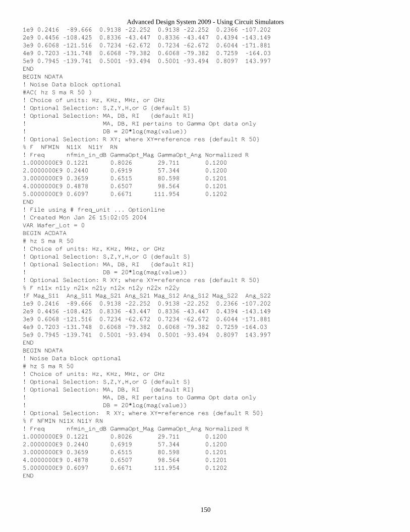
Advanced Design System 2009 - Using Circuit Simulators
150
1e9 0.2416 -89.666 0.9138 -22.252 0.9138 -22.252 0.2366 -107.202
2e9 0.4456 -108.425 0.8336 -43.447 0.8336 -43.447 0.4394 -143.149
3e9 0.6068 -121.516 0.7234 -62.672 0.7234 -62.672 0.6044 -171.881
4e9 0.7203 -131.748 0.6068 -79.382 0.6068 -79.382 0.7259 -164.03
5e9 0.7945 -139.741 0.5001 -93.494 0.5001 -93.494 0.8097 143.997
END
BEGIN NDATA
! Noise Data block optional
#AC( hz S ma R 50 )
! Choice of units: Hz, KHz, MHz, or GHz
! Optional Selection: S,Z,Y,H,or G {default S}
! Optional Selection: MA, DB, RI {default RI}
! MA, DB, RI pertains to Gamma Opt data only
! DB = 20*log(mag(value))
! Optional Selection: R XY; where XY=reference res {default R 50}
% F NFMIN N11X N11Y RN
! Freq nfmin_in_dB GammaOpt_Mag GammaOpt_Ang Normalized R
1.0000000E9 0.1221 0.8026 29.711 0.1200
2.0000000E9 0.2440 0.6919 57.344 0.1200
3.0000000E9 0.3659 0.6515 80.598 0.1201
4.0000000E9 0.4878 0.6507 98.564 0.1201
5.0000000E9 0.6097 0.6671 111.954 0.1202
END
! File using # freq_unit ... Optionline
! Created Mon Jan 26 15:02:05 2004
VAR Wafer_Lot = 0
BEGIN ACDATA
# hz S ma R 50
! Choice of units: Hz, KHz, MHz, or GHz
! Optional Selection: S,Z,Y,H,or G {default S}
! Optional Selection: MA, DB, RI {default RI}
! DB = 20*log(mag(value))
! Optional Selection: R XY; where XY=reference res {default R 50}
% F n11x n11y n21x n21y n12x n12y n22x n22y
!F Mag_S11 Ang_S11 Mag_S21 Ang_S21 Mag_S12 Ang_S12 Mag_S22 Ang_S22
1e9 0.2416 -89.666 0.9138 -22.252 0.9138 -22.252 0.2366 -107.202
2e9 0.4456 -108.425 0.8336 -43.447 0.8336 -43.447 0.4394 -143.149
3e9 0.6068 -121.516 0.7234 -62.672 0.7234 -62.672 0.6044 -171.881
4e9 0.7203 -131.748 0.6068 -79.382 0.6068 -79.382 0.7259 -164.03
5e9 0.7945 -139.741 0.5001 -93.494 0.5001 -93.494 0.8097 143.997
END
BEGIN NDATA
! Noise Data block optional
# hz S ma R 50
! Choice of units: Hz, KHz, MHz, or GHz
! Optional Selection: S,Z,Y,H,or G {default S}
! Optional Selection: MA, DB, RI {default RI}
! MA, DB, RI pertains to Gamma Opt data only
! DB = 20*log(mag(value))
! Optional Selection: R XY; where XY=reference res {default R 50}
% F NFMIN N11X N11Y RN
! Freq nfmin_in_dB GammaOpt_Mag GammaOpt_Ang Normalized R
1.0000000E9 0.1221 0.8026 29.711 0.1200
2.0000000E9 0.2440 0.6919 57.344 0.1200
3.0000000E9 0.3659 0.6515 80.598 0.1201
4.0000000E9 0.4878 0.6507 98.564 0.1201
5.0000000E9 0.6097 0.6671 111.954 0.1202
END
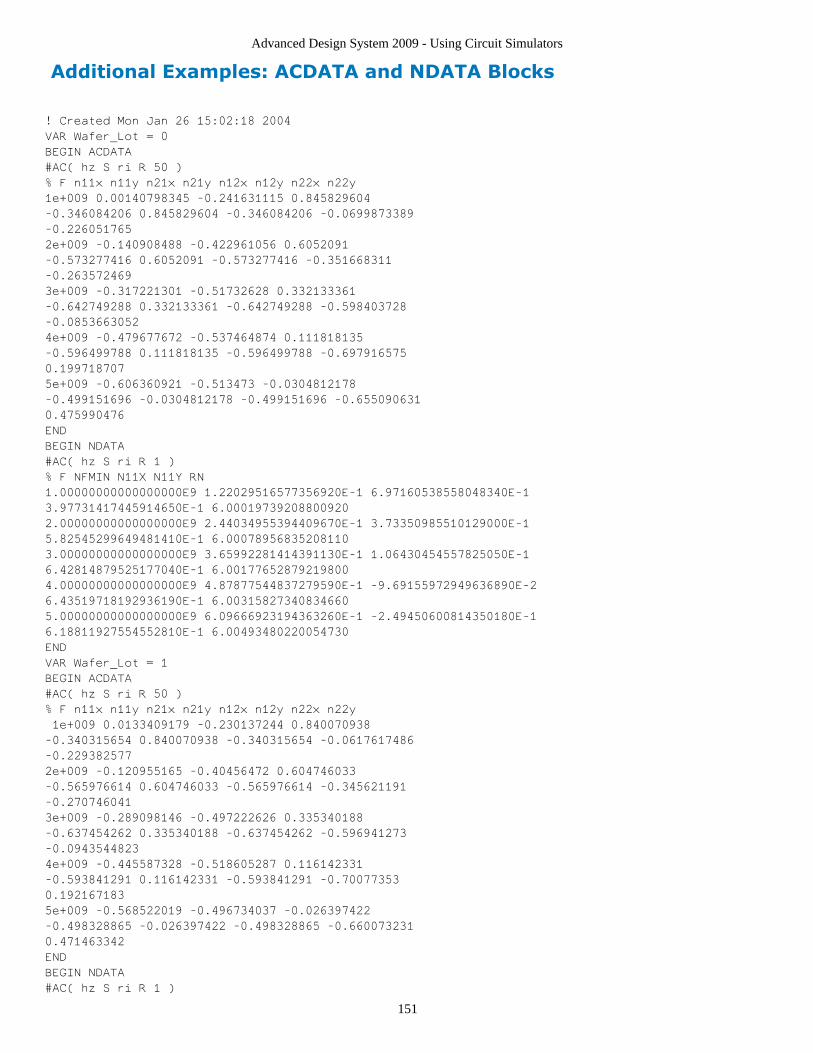
Advanced Design System 2009 - Using Circuit Simulators
151
Additional Examples: ACDATA and NDATA Blocks
! Created Mon Jan 26 15:02:18 2004
VAR Wafer_Lot = 0
BEGIN ACDATA
#AC( hz S ri R 50 )
% F n11x n11y n21x n21y n12x n12y n22x n22y
1e+009 0.00140798345 -0.241631115 0.845829604
-0.346084206 0.845829604 -0.346084206 -0.0699873389
-0.226051765
2e+009 -0.140908488 -0.422961056 0.6052091
-0.573277416 0.6052091 -0.573277416 -0.351668311
-0.263572469
3e+009 -0.317221301 -0.51732628 0.332133361
-0.642749288 0.332133361 -0.642749288 -0.598403728
-0.0853663052
4e+009 -0.479677672 -0.537464874 0.111818135
-0.596499788 0.111818135 -0.596499788 -0.697916575
0.199718707
5e+009 -0.606360921 -0.513473 -0.0304812178
-0.499151696 -0.0304812178 -0.499151696 -0.655090631
0.475990476
END
BEGIN NDATA
#AC( hz S ri R 1 )
% F NFMIN N11X N11Y RN
1.00000000000000000E9 1.22029516577356920E-1 6.97160538558048340E-1
3.97731417445914650E-1 6.00019739208800920
2.00000000000000000E9 2.44034955394409670E-1 3.73350985510129000E-1
5.82545299649481410E-1 6.00078956835208110
3.00000000000000000E9 3.65992281414391130E-1 1.06430454557825050E-1
6.42814879525177040E-1 6.00177652879219800
4.00000000000000000E9 4.87877544837279590E-1 -9.69155972949636890E-2
6.43519718192936190E-1 6.00315827340834660
5.00000000000000000E9 6.09666923194363260E-1 -2.49450600814350180E-1
6.18811927554552810E-1 6.00493480220054730
END
VAR Wafer_Lot = 1
BEGIN ACDATA
#AC( hz S ri R 50 )
% F n11x n11y n21x n21y n12x n12y n22x n22y
1e+009 0.0133409179 -0.230137244 0.840070938
-0.340315654 0.840070938 -0.340315654 -0.0617617486
-0.229382577
2e+009 -0.120955165 -0.40456472 0.604746033
-0.565976614 0.604746033 -0.565976614 -0.345621191
-0.270746041
3e+009 -0.289098146 -0.497222626 0.335340188
-0.637454262 0.335340188 -0.637454262 -0.596941273
-0.0943544823
4e+009 -0.445587328 -0.518605287 0.116142331
-0.593841291 0.116142331 -0.593841291 -0.70077353
0.192167183
5e+009 -0.568522019 -0.496734037 -0.026397422
-0.498328865 -0.026397422 -0.498328865 -0.660073231
0.471463342
END
BEGIN NDATA
#AC( hz S ri R 1 )
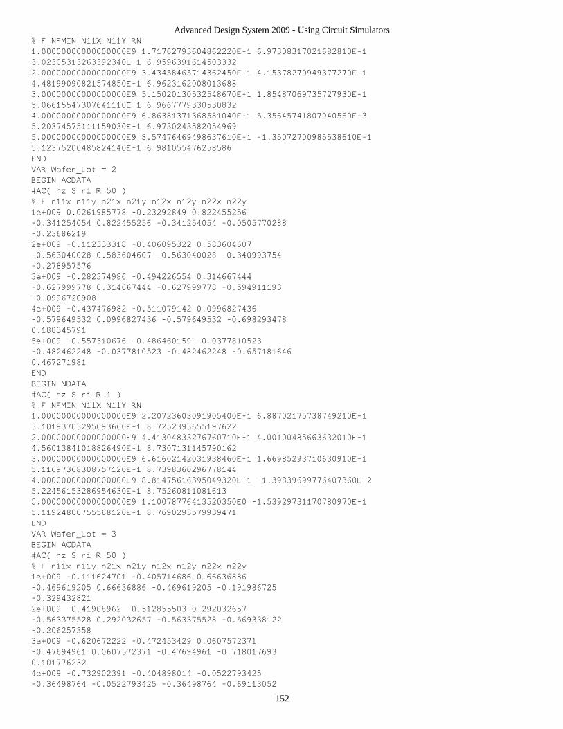
Advanced Design System 2009 - Using Circuit Simulators
152
% F NFMIN N11X N11Y RN
1.00000000000000000E9 1.71762793604862220E-1 6.97308317021682810E-1
3.02305313263392340E-1 6.9596391614503332
2.00000000000000000E9 3.43458465714362450E-1 4.15378270949377270E-1
4.48199090821574850E-1 6.9623162008013688
3.00000000000000000E9 5.15020130532548670E-1 1.85487069735727930E-1
5.06615547307641110E-1 6.9667779330530832
4.00000000000000000E9 6.86381371368581040E-1 5.35645741807940560E-3
5.20374575111159030E-1 6.9730243582054969
5.00000000000000000E9 8.57476469498637610E-1 -1.35072700985538610E-1
5.12375200485824140E-1 6.981055476258586
END
VAR Wafer_Lot = 2
BEGIN ACDATA
#AC( hz S ri R 50 )
% F n11x n11y n21x n21y n12x n12y n22x n22y
1e+009 0.0261985778 -0.23292849 0.822455256
-0.341254054 0.822455256 -0.341254054 -0.0505770288
-0.23686219
2e+009 -0.112333318 -0.406095322 0.583604607
-0.563040028 0.583604607 -0.563040028 -0.340993754
-0.278957576
3e+009 -0.282374986 -0.494226554 0.314667444
-0.627999778 0.314667444 -0.627999778 -0.594911193
-0.0996720908
4e+009 -0.437476982 -0.511079142 0.0996827436
-0.579649532 0.0996827436 -0.579649532 -0.698293478
0.188345791
5e+009 -0.557310676 -0.486460159 -0.0377810523
-0.482462248 -0.0377810523 -0.482462248 -0.657181646
0.467271981
END
BEGIN NDATA
#AC( hz S ri R 1 )
% F NFMIN N11X N11Y RN
1.00000000000000000E9 2.20723603091905400E-1 6.88702175738749210E-1
3.10193703295093660E-1 8.7252393655197622
2.00000000000000000E9 4.41304833276760710E-1 4.00100485663632010E-1
4.56013841018826490E-1 8.7307131145790162
3.00000000000000000E9 6.61602142031938460E-1 1.66985293710630910E-1
5.11697368308757120E-1 8.7398360296778144
4.00000000000000000E9 8.81475616395049320E-1 -1.39839699776407360E-2
5.22456153286954630E-1 8.75260811081613
5.00000000000000000E9 1.10078776413520350E0 -1.53929731170780970E-1
5.11924800755568120E-1 8.7690293579939471
END
VAR Wafer_Lot = 3
BEGIN ACDATA
#AC( hz S ri R 50 )
% F n11x n11y n21x n21y n12x n12y n22x n22y
1e+009 -0.111624701 -0.405714686 0.66636886
-0.469619205 0.66636886 -0.469619205 -0.191986725
-0.329432821
2e+009 -0.41908962 -0.512855503 0.292032657
-0.563375528 0.292032657 -0.563375528 -0.569338122
-0.206257358
3e+009 -0.620672222 -0.472453429 0.0607572371
-0.47694961 0.0607572371 -0.47694961 -0.718017693
0.101776232
4e+009 -0.732902391 -0.404898014 -0.0522793425
-0.36498764 -0.0522793425 -0.36498764 -0.69113052

Advanced Design System 2009 - Using Circuit Simulators
153
0.390569198
5e+009 -0.795560017 -0.34381194 -0.101065286
-0.269885315 -0.101065286 -0.269885315 -0.576309143
0.608680065
END
BEGIN NDATA
#AC( hz S ri R 1 )
% F NFMIN N11X N11Y RN
1.00000000000000000E9 5.18703037517405720E-1 2.56297603514494640E-1
5.77469208317883620E-1 9.5231179096495424
2.00000000000000000E9 1.03556771684315740E0 -2.06911574434137120E-1
5.86373914380050380E-1 9.5447677385981624
3.00000000000000000E9 1.54881350043704070E0 -4.46640278565243860E-1
5.11094686752464700E-1 9.5808507868458594
4.00000000000000000E9 2.05677054388418230E0 -5.81970283235218930E-1
4.38893368283120290E-1 9.6313670543926495
5.00000000000000000E9 2.55792347993451760E0 -6.65702281631675600E-1
3.80285542816346120E-1 9.6963165412384953
END
VAR Wafer_Lot = 4
BEGIN ACDATA
#AC( hz S ri R 50 )
% F n11x n11y n21x n21y n12x n12y n22x n22y
1e+009 -0.0997555774 -0.381004445 0.705619581
-0.459619141 0.705619581 -0.459619141 -0.188617047
-0.322113995
2e+009 -0.387429707 -0.50652345 0.338299265
-0.580037701 0.338299265 -0.580037701 -0.568533379
-0.21853959
3e+009 -0.59300033 -0.48258943 0.0913926446
-0.508488094 0.0913926446 -0.508488094 -0.734058749
0.0900874159
4e+009 -0.71385299 -0.421239785 -0.0364444847
-0.397584211 -0.0364444847 -0.397584211 -0.713634507
0.390775305
5e+009 -0.783429944 -0.361124669 -0.0944553209
-0.298630566 -0.0944553209 -0.298630566 -0.595965263
0.61920336
END
BEGIN NDATA
#AC( hz S ri R 1 )
% F NFMIN N11X N11Y RN
1.00000000000000000E9 4.07278952069115260E-1 3.20981863953611680E-1
5.26706311842366580E-1 7.6643738931871832
2.00000000000000000E9 8.13665870677917270E-1 -1.24308690147576310E-1
5.64368849214357040E-1 7.6773474702487121
3.00000000000000000E9 1.21828615365247780E0 -3.71333282289684650E-1
5.08578990984615050E-1 7.6989700986845886
4.00000000000000000E9 1.62029912735584050E0 -5.17462235668050940E-1
4.46062394082844540E-1 7.7292417784948277
5.00000000000000000E9 2.01891277231332160E0 -6.10837572225724480E-1
3.92061347849876940E-1 7.7681625096794225
END
VAR Wafer_Lot = 5
BEGIN ACDATA
#AC( hz S ri R 50 )
% F n11x n11y n21x n21y n12x n12y n22x n22y
1e+009 -0.148708863 -0.411149613 0.661371247
-0.487106054 0.661371247 -0.487106054 -0.245385025
-0.343281312
2e+009 -0.459669272 -0.498617399 0.27661003

Advanced Design System 2009 - Using Circuit Simulators
154
-0.561103773 0.27661003 -0.561103773 -0.633354256
-0.183147263
3e+009 -0.65008453 -0.447693986 0.054820678
-0.464075002 0.054820678 -0.464075002 -0.761781857
0.147962113
4e+009 -0.751951738 -0.378576048 -0.0489188832
-0.35214127 -0.0489188832 -0.35214127 -0.712725662
0.441632279
5e+009 -0.807697362 -0.319231466 -0.0924561924
-0.260818351 -0.0924561924 -0.260818351 -0.581417298
0.655785284
END
BEGIN NDATA
#AC( hz S ri R 1 )
% F NFMIN N11X N11Y RN
1.00000000000000000E9 4.82467789743262190E-1 2.28415357401098710E-1
5.09316970466515430E-1 7.1489835897047316
2.00000000000000000E9 9.63454968428843020E-1 -2.06744364689974120E-1
5.11947374976623950E-1 7.1696884038188884
3.00000000000000000E9 1.44152132366022330E0 -4.32828356211392770E-1
4.47558248165678220E-1 7.2041964273425005
4.00000000000000000E9 1.91530443304156290E0 -5.63042210953368820E-1
3.86155387977519470E-1 7.2525076602755627
5.00000000000000000E9 2.38355146947575140E0 -6.45263220258679840E-1
3.36048596462367750E-1 7.3146221026180545
END
P2D Format The large-signal or power-dependent S-parameter (.p2d) file is a system input file youcreate from an S-parameter file, inserting the MDIF format. You use the . p2d file tocharacterize the component by a complete set of 2-port large-signal S-parameters,accounting for power dependence of S21, S11, S22, and S12, plus optional noise data,and optional intermodulation data.
A .p2d file can also be created via simulation by placing a P2D simulation component fromthe LSSP Simulation Library in the design.
It possible to have multi-dimensional P2D files with VAR statements separating individualbasic P2D sections. Such files may be automatically generated using theAmplifierP2D_Setup component from the System-Data Models library.
The format for a basic P2D section is shown here. Required keywords appear inUPPERCASE ITALIC characters.
!!! Begin basic P2D syntaxBEGIN ACDATA !!! required 2-port S-parameter data block..... ( Required small signal section identical to ACDATA section of S2Dformat )..... ( Optional large signal section - shown in the next section )END ACDATABEGIN NDATA !!! optional 2-port noise data block....

Advanced Design System 2009 - Using Circuit Simulators
155
END NDATABEGIN IMTDATA !!! optional intermodulation table....END IMTDATA!!! End basic P2D syntax
This format can be expanded to form a multi-dimensional P2D file using VAR statements.For instance a single P2D file containing two temperature points over three bias pointscontains a total of six basic sections as shown. Note that each sequence of VARstatements should preserve the order of the sweep, in this case temperature over biasand each sweep variable, for example, bias has its values arranged in monotonicallyincreasing order. In this example B1 < B2 < B3 and T1 < T2 . Required keywords appearin UPPERCASE ITALIC characters.
VAR temp=T1VAR bias=B1...... ( 1st Basic P2D section )VAR temp=T1VAR bias=B2...... ( 2nd Basic P2D section )VAR temp=T1VAR bias=B3...... ( 3rd Basic P2D section )VAR temp=T2VAR bias=B1...... ( 4th Basic P2D section )VAR temp=T2VAR bias=B2...... ( 5th Basic P2D section )VAR temp=T2VAR bias=B3...... ( 6th Basic P2D section )
Guidelines for .p2d
Basic MDIF syntax contains four reserved words. VAR begins an independent variabledefinition line, in the form VAR <name> = <value>. BEGIN <blockname> signals thebeginning of a data block, and END signals the conclusion of a data block. A linebeginning with REM or the comment symbol (!) will be assumed as comments.VAR statements are used to specify multidimensional data, that is, two or moreindependent variables. The value of a VAR statement can be a number.Multiple sets of data (ACDATA, NDATA, IMTDATA) can be used with VAR statementsused before or after any dataset.The file dataset is made up of data blocks, each separated by BEGIN and ENDstatements. Three different types of data blocks are allowed:

Advanced Design System 2009 - Using Circuit Simulators
156
ACDATA = Lists small and large-signal parameters vs. frequency and power (required)
NDATA = Lists noise parameters vs. frequency (optional)
IMTDATA = Used for a 2-port frequency converter to give the single-tone intermodulation table(optional)
The ACDATA Block
The ACDATA block allows you to specify the small- and large-signal characteristics of the2-port.
General format:BEGIN ACDATA# AC ( ....... ) ! this is the option line% .... ! this is a format line __..... small-signal data goes here% F ! this is a format line... first large-signal data frequency% P1 P2 ..... ! this is a format line... large-signal data at first frequency% F ! next large-signal frequency... second large-signal data frequency% P1 P2 ....... large-signal data at second frequency...... additional sets of large- signal frequency and data...ENDOption line:# AC( unit parm_type parm_format R xx FC m b )where:unit = Sets the frequency unit.
Options are HZ, KHZ, MHZ, or GHZ.
parm_type = Only S-parameters are allowed; use S only.
parm_format = MA, DB, RI, VDB sets the format for the four network parameters, where:MA declares magnitude and angle (degrees)DB is for 20 • log10( MA) and angle (degrees)RI declares real and imaginaryVDB declares n11 and n22 as VSWR and angle (degrees) and n21 and n12 as DB andangle (degrees)
R xx = Declares resistance, where xx = normalization resistance.
FC m b = Declares input to output frequency conversion whereFout = m • Fin + b ; where:m is for frequency multiplicationb is for frequency translation
Small-signal format line:% F n11x n11y n21x n21y n12x n12y n22x n22yThis line gives the order for the data in the lines to follow. All of the keywords shownmust be given in the format line. The order of these keywords is arbitrary. The ordershown is preferred.

Advanced Design System 2009 - Using Circuit Simulators
157
F = For frequency data
n11x, n11y = The 11 data pair for the 2 port data matrix
n21x, n21y = The 21 data pair
n12x, n12y = The 12 data pair
n22x, n22y = The 22 data pair
If the parameter type = S, and the parameter format = DB, thenn11x = |S11| in dB, and n11y = angle of S11 in degrees.Large-signal format line:% FThis line precedes the frequency for the following large-signal data.% P1 P2 n11x n11y n21x n21y n12x n12y n22x n22yThis line precedes the large-signal data. The large-signal data may have up to 101sets of power data per frequency.All of the keywords shown must be given in the format line. While the order ofkeywords is arbitrary, the order shown is preferred.P1 = The power (dBm) incident at port 1 with port 2 terminated in R ohms, for the measurement of
S11 and S21
P2 = The power (dBm) incident at port 2 with port 1 terminated in R ohms, for the measurement ofS22 and S12
In the following data, a value of 1000 (1.e3) for the P2 data indicates that the S22and S12 data are for small-signal measurement.
n11x, n11y = The 11 data pair for the 2 port data matrix
n21x, n21y = The 21 data pair
n12x, n12y = The 12 data pair
n22x, n22y = The 22 data pair
If the parameter type = S, and the parameter format = DB, then n11x = |S11| indB, and n11y = angle of S11 in degrees.
ACDATA Block Examples
2-port with 50-ohm S-parameters:
BEGIN ACDATA
# AC( GHZ S DB R 50 FC 1.0 0.0 )
% F n11x n11y n21x n21y n12x n12y n22x n22y
! RF-freq S11-db S11-deg S21-dB S21-deg S12-dB S12-deg S22-db S22-deg

Advanced Design System 2009 - Using Circuit Simulators
158
1.0000 -15 45 8 25 -20 -15 -12 10
2.0000 -16 25 9 30 -20 -15 -12 20
3.0000 -17 -10 10 35 -20 -15 -11 30
% F
1.00
% P1 P2 n11x n11y n21x n21y n12x n12y n22x n22y
-15.000 -5.000 ...
-5.000 5.000 ... large-signal S-parameter data here ...
5.020 15.000 ...
% F
2.00
% P1 P2 n11x n11y n21x n21y n12x n12y n22x n22y
-15.000 -5.000 ...
-5.000 5.000 ... large-signal S-parameter data here ...
5.020 15.000 ...
END
2-port frequency converter with variable RF freq, variable LO freq, fixed IF freq, fixed LOpower, and RF-to-IF 2-port 50-ohm S-parameters:
BEGIN ACDATA
# AC( GHZ VDB R 50 FC 0 0.2 ) ! this gives a constant IF of 0.2 GHz
% F n11x n11y n21x n21y n12x n12y n22x n22y
! RF-freq S11-vswr S11-deg S21-dB S21-deg S12-dB S12-deg S22-vswr S22-deg
1.0000 1.2 0 -8 0 -20 0 1.3 0
2.0000 1.3 0 -9 0 -20 0 1.2 0
3.0000 1.4 0 -10 0 -20 0 1.3 0
% F
1.00
% P1 P2 n11x n11y n21x n21y n12x n12y n22x n22y
-15.000 -5.00 ...
-5.000 5.00 ... large-signal S-parameter data here ...
5.020 15.00 ...
% F
2.00
% P1 P2 n11x n11y n21x n21y n12x n12y n22x n22y
-15.000 -5.00 ...
-5.000 5.00 ... large-signal S-parameter data here ...
5.020 15.00 ...
END
2-port frequency converter with variable RF freq, fixed LO freq, variable IF freq, fixed LOpower, and RF-to-IF 2 port 50-ohm S-parameters:
BEGIN ACDATA
# AC( GHZ DB R 50 FC -1 4 ) ! this gives an IF = 4 - RF
% F n11x n11y n21x n21y n12x n12y n22x n22y
! RF-freq S11-dB S11-deg S21-dB S21-dB S12-dB S12-deg S22-dB S22-deg
1.0000 -12 0 -8 0 -20 0 -13 0
2.0000 -13 0 -9 0 -20 0 -12 0
3.0000 -14 0 -10 0 -20 0 -13 0
% F
1000.00
% P1 P2 n11x n11y n21x n21y n12x n12y n22x n22y
-15.000 -5.00 ...
-5.000 5.00 ... large-signal S-parameter data here ...
5.020 15.00 ...
% F

Advanced Design System 2009 - Using Circuit Simulators
159
2000.00
% P1 P2 n11x n11y n21x n21y n12x n12y n22x n22y
-15.000 -5.00 ...
-5.000 5.00 ... large-signal S-parameter data here ...
5.020 15.00 ...
END
The NDATA Block
The NDATA block allows the user to specify the small-signal noise characteristics of the 2-port.
General format:BEGIN NDATA# AC ( ....... ) ! this is the option line% .... ! this is the format line..... data goes hereENDOption line:# AC( freq_unit parm_type parm_format R xx )where:freq_unit = Sets the frequency unit.
Options are HZ, KHZ, MHZ, or GHZ.
parm_type = S sets the source noise match type to optimum source reflection coefficient.
parm_format = MA, DB, RI sets the format for the optimum source match, where:MA declares magnitude and angle (degrees)DB declares 20 • log10( MA) and angle (degrees)RI declares real and imaginary
R xx = Declares resistance, where xx = normalization resistance for the source match and rn.
Format line:% F nfmin n11x n11y rnThis line gives the order for the data in the lines to follow. All of the keywords shownmust be given in the format line. While the order of keywords is arbitrary, the ordershown is preferredF = For frequency data
nfmin = For minimum noise figure data
n11x,n11y
= For the optimum source impedance for minimum noise figure
rn = For the equivalent input normalized noise resistance. The system simulator requires thisparameter to meet physical requirements. If the user-supplied rn value is less than allowedfor this requirement, then the system simulator will force this rn value to the lowest physicallimit.
The IMTDATA Block
The IMTDATA data block allows you to specify for a 2-port frequency converter the singletone output intermodulation levels with respect to the fundamental output tone.
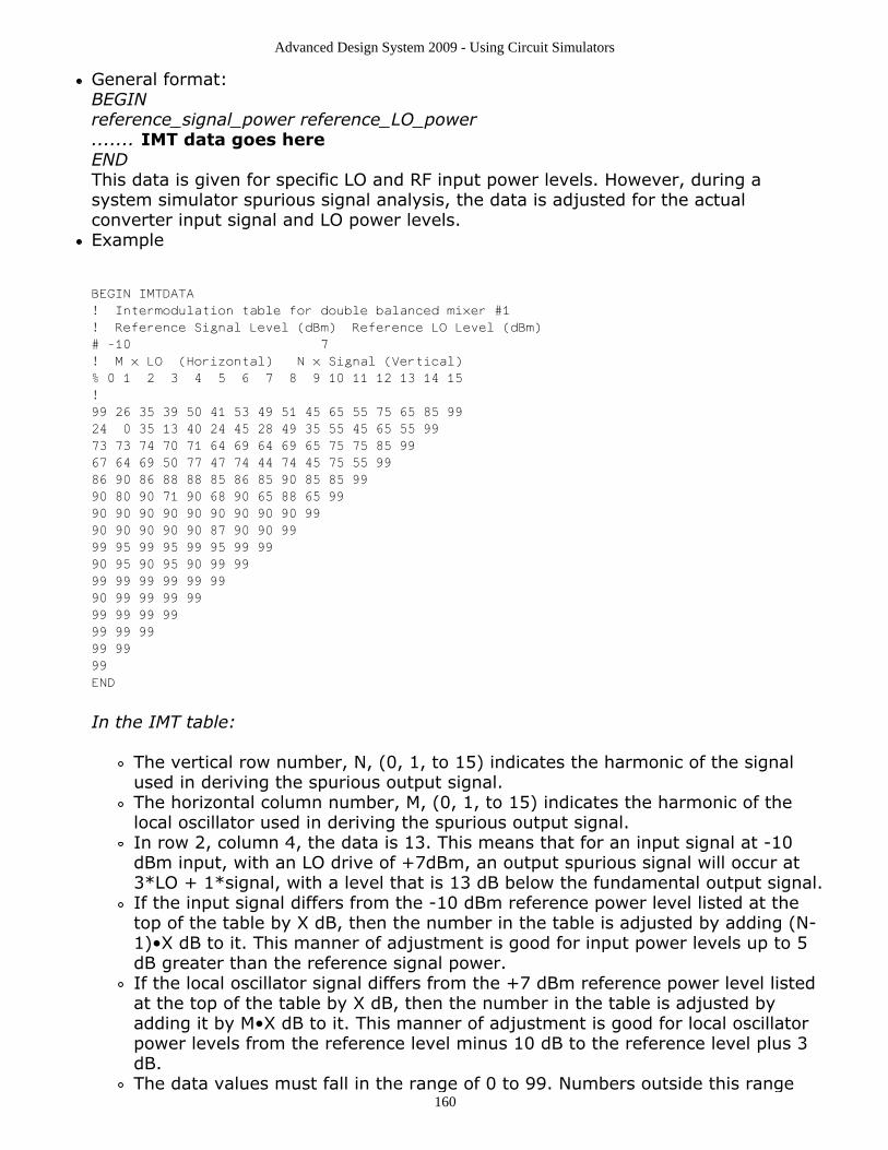
Advanced Design System 2009 - Using Circuit Simulators
160
General format:BEGINreference_signal_power reference_LO_power....... IMT data goes hereENDThis data is given for specific LO and RF input power levels. However, during asystem simulator spurious signal analysis, the data is adjusted for the actualconverter input signal and LO power levels.Example
BEGIN IMTDATA
! Intermodulation table for double balanced mixer #1
! Reference Signal Level (dBm) Reference LO Level (dBm)
# -10 7
! M x LO (Horizontal) N x Signal (Vertical)
% 0 1 2 3 4 5 6 7 8 9 10 11 12 13 14 15
!
99 26 35 39 50 41 53 49 51 45 65 55 75 65 85 99
24 0 35 13 40 24 45 28 49 35 55 45 65 55 99
73 73 74 70 71 64 69 64 69 65 75 75 85 99
67 64 69 50 77 47 74 44 74 45 75 55 99
86 90 86 88 88 85 86 85 90 85 85 99
90 80 90 71 90 68 90 65 88 65 99
90 90 90 90 90 90 90 90 90 99
90 90 90 90 90 87 90 90 99
99 95 99 95 99 95 99 99
90 95 90 95 90 99 99
99 99 99 99 99 99
90 99 99 99 99
99 99 99 99
99 99 99
99 99
99
END
In the IMT table:
The vertical row number, N, (0, 1, to 15) indicates the harmonic of the signalused in deriving the spurious output signal.The horizontal column number, M, (0, 1, to 15) indicates the harmonic of thelocal oscillator used in deriving the spurious output signal.In row 2, column 4, the data is 13. This means that for an input signal at -10dBm input, with an LO drive of +7dBm, an output spurious signal will occur at3*LO + 1*signal, with a level that is 13 dB below the fundamental output signal.If the input signal differs from the -10 dBm reference power level listed at thetop of the table by X dB, then the number in the table is adjusted by adding (N-1)•X dB to it. This manner of adjustment is good for input power levels up to 5dB greater than the reference signal power.If the local oscillator signal differs from the +7 dBm reference power level listedat the top of the table by X dB, then the number in the table is adjusted byadding it by M•X dB to it. This manner of adjustment is good for local oscillatorpower levels from the reference level minus 10 dB to the reference level plus 3dB.The data values must fall in the range of 0 to 99. Numbers outside this range
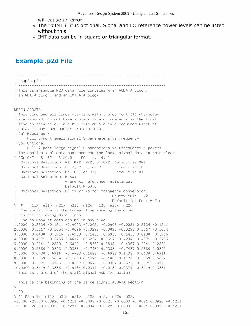
Advanced Design System 2009 - Using Circuit Simulators
161
will cause an error.The "#IMT ( )" is optional. Signal and LO reference power levels can be listedwithout this.IMT data can be in square or triangular format.
Example .p2d File
! ------------------------------------------------------------------
! ampp2d.p2d
! ------------------------------------------------------------------
! This is a sample P2D data file containing an ACDATA block,
! an NDATA block, and an IMTDATA block.
! ------------------------------------------------------------------
!
BEGIN ACDATA
! This line and all lines starting with the comment (!) character
! are ignored. Do not have a blank line or comments as the first
! line in this file. In a P2D file ACDATA is a required block of
! data. It may have one or two sections.
! (a) Required -
! Full 2-port small signal S-parameters vs frequency
! (b) Optional -
! Full 2-port large signal S-parameters vs (frequency X power)
! The small signal data must precede the large signal data in this block.
# AC( GHZ S RI R 50.0 FC 1. 0. )
! Optional Selection: HZ, KHZ, MKZ, or GHZ; Default is GHZ
! Optional Selection: S, Z, Y, H, or G; Default is S
! Optional Selection: MA, DB, or RI; Default is RI
! Optional Selection: R xx;
! where xx=reference resistance;
! Default R 50.0
! Optional Selection: FC x1 x2 is for frequency conversion:
! Fout=x1*Fin + x2
! Default is Fout = Fin
% F n11x n11y n21x n21y n12x n12y n22x n22y
! The above line is the format line showing the order
! in the following data lines
! The columns of data can be in any order
1.0000 0.3926 -0.1211 -0.0003 -0.0021 -0.0003 -0.0021 0.3926 -0.1211
2.0000 0.3517 -0.3054 -0.0096 -0.0298 -0.0096 -0.0298 0.3517 -0.3054
3.0000 0.0430 -0.5916 -2.6933 -0.1433 -0.5933 -0.1433 0.0430 -0.5916
4.0000 0.4071 -0.2756 2.4617 0.6234 0.3617 0.4234 0.4071 -0.2756
5.0000 0.2041 0.2880 2.6848 -0.5367 0.3848 -0.4367 0.2041 0.2880
6.0000 0.5666 0.0343 2.0383 -0.7437 0.0383 -0.7437 0.5666 0.0343
7.0000 0.0430 0.6916 -2.6933 0.1433 -0.6933 0.1433 0.0430 0.6916
8.0000 0.3059 0.5659 -0.1000 0.1424 -0.1000 0.1424 0.3059 0.5659
9.0000 0.3071 0.4145 -0.0307 0.0673 -0.0307 0.0673 0.3071 0.4145
10.0000 0.3419 0.3336 -0.0134 0.0379 -0.0134 0.0379 0.3419 0.3336
! This is the end of the small signal ACDATA section
!
! This is the beginning of the large signal ACDATA section
% F
1.00
% P1 P2 n11x n11y n21x n21y n12x n12y n22x n22y
-15.00 -25.00 0.3926 -0.1211 -0.0003 -0.0021 -0.0003 -0.0021 0.3926 -0.1211
-10.00 -20.00 0.3826 -0.1221 -0.0004 -0.0022 -0.0003 -0.0021 0.3926 -0.1211

Advanced Design System 2009 - Using Circuit Simulators
162
-5.00 -15.00 0.3726 -0.1231 -0.0007 -0.0029 -0.0003 -0.0021 0.3926 -0.1211
0.00 -10.00 0.3856 -0.1245 -0.0010 -0.0129 -0.0003 -0.0021 0.3926 -0.1211
% F
2.00
% P1 P2 n11x n11y n21x n21y n12x n12y n22x n22y
-15.00 -25.00 0.3517 -0.3054 -0.0096 -0.0298 -0.0096 -0.0298 0.3517 -0.3054
-10.00 -20.00 0.3517 -0.3154 -0.0098 -0.0298 -0.0096 -0.0298 0.3517 -0.3054
-5.00 -15.00 0.3517 -0.3254 -0.0104 -0.0298 -0.0096 -0.0298 0.3517 -0.3054
0.00 -10.00 0.3517 -0.3354 -0.0106 -0.0298 -0.0096 -0.0298 0.3517 -0.3054
! ... (more frequencies and power sweeps under each frequency may be added)
! This is the end of the small signal ACDATA section
END
BEGIN NDATA
! This is an optional block of data
# AC( GHZ RI S R 50.0 )
! Optional Selection: HZ, KHZ, MKZ, or GHZ; Default is GHZ
! Optional Selection: S, Z, Y, H, or G; Default is S
! Optional Selection: MA, DB, or RI; Default is RI
! Optional Selection: R xx; where xx = reference resistance;
! Default R 50.0
% F nfmin n11x n11y rn
! The above line is the format line showing the order
! in the following data lines
! The columns of data can be in any order
1.0000 2.0000 0.3926 -0.1211 .4
2.0000 2.5000 0.3517 -0.3054 .45
3.0000 3.0000 0.0430 -0.5916 .5
4.0000 3.5000 0.4071 -0.2756 .55
5.0000 4.0000 0.2041 0.2880 .6
6.0000 4.5000 0.5666 0.0343 .65
7.0000 5.0000 0.0430 0.6916 .7
8.0000 5.5000 0.3059 0.5659 .75
9.0000 6.0000 0.3071 0.4145 .8
10.0000 6.5000 0.3419 0.3336 .85
END
BEGIN IMTDATA
! This is an optional block and may be used
! some mixer component if the file
! format is supported.
! Intermodulation table for double balanced mixer #1
! Signal Level (dBm) LO Level (dBm)
# -10 7
! M x LO ( Horizontal ) N x Signal (Vertical )
! 0 1 2 3 4 5 6 7 8 9 10 11 12 13 14 15
!
99 26 35 39 50 41 53 49 51 42 62 51 60 47 77 50
24 0 35 13 40 24 45 28 49 33 53 42 60 47 63
73 73 74 70 71 64 69 64 69 62 74 62 72 60
67 64 69 50 77 47 74 44 74 47 75 44 70
86 90 86 88 88 85 86 85 90 85 85 85
90 80 90 71 90 68 90 65 88 65 85
90 90 90 90 90 90 90 90 90 90
90 90 90 90 90 87 90 90 90
99 95 99 95 99 95 99 95
90 95 90 90 90 99 90
99 99 99 99 99 99
90 99 90 95 90
99 99 99 99
90 99 90
99 99
99

Advanced Design System 2009 - Using Circuit Simulators
163
END
!
! ------------------------------------------------------------------
S2D Format The S-parameter Data (.s2d ) file is a system input file you create from an S-parameterfile, inserting the MDIF format. In the .s2d file, you describe small-signal data, optionalnoise data, optional nonlinear data, and optional intermodulation data. You can describenonlinearity as a function of drive power or nonlinear parameter consisting of somecombination of third-order intercept point, 1dB gain compression, saturated output power,and gain compression at saturation. In ADS, it possible to have multidimensional S2D fileswith VAR statements separating individual basic S2D sections. Such files may beautomatically generated using the AmplifierS2D_Setup component from the System-DataModels library.
The format for a basic S2D section is shown here. Required keywords appear inUPPERCASE ITALIC characters.
!!! Begin basic S2D syntaxBEGIN ACDATA !!! optional small-signal data block....END ACDATABEGIN GCOMPx !!! required compression information x=(1,...,7)!!! only one type of GCOMPx supported in one S2D file....END GCOMPxBEGIN NDATA !!! optional 2-port noise data block....END NDATABEGIN IMTDATA !!! optional intermodulation table....END IMTDATA!!! End basic S2D syntax
This format can be expanded to form a multi-dimensional S2D file using VAR statementsin ADS. For instance a single S2D file containing two temperature points over three biaspoints contains a total of six basic sections as shown. Note that each sequence of VARstatements should preserve the order of the sweep, in this case, temperature over biasand each sweep variable. For example, bias has its values arranged in monotonicallyincreasing order. In this example B1 < B2 < B3 and T1 < T2. Required keywords appearin UPPERCASE ITALIC characters:
VAR temp=T1VAR bias=B1...... ( 1st basic S2D section )VAR temp=T1VAR bias=B2...... ( 2nd basic S2D section )

Advanced Design System 2009 - Using Circuit Simulators
164
VAR temp=T1VAR bias=B3...... ( 3rd basic S2D section )VAR temp=T2VAR bias=B1...... ( 4th basic S2D section )VAR temp=T2VAR bias=B2...... ( 5th basic S2D section )VAR temp=T2VAR bias=B3...... ( 6th basic S2D section )
Guidelines for .s2d
Basic MDIF syntax contains four reserved words:VAR begins an independent variable definition line, in the form VAR <name> =<value>.BEGIN <blockname> signals the beginning of a data block.END signals the conclusion of a data block.REM or the comment symbol (!) at the beginning of a line signifies a comment.
VAR statements are used to specify multidimensional data, that is, two or moreindependent variables. The value of a VAR statement can be a number.Comments can be inserted on any line within the file and must be preceded by acomment symbol (!).Multiple sets of data (ACDATA, NDATA, GCOMP, IMTDATA) can be used with VARstatements before or after any dataset. Note that only one type of GCOMP block canbe used in a single S2D file, for instance do not create an S2D file containing oneGCOMP3 and one GCOMP5 block.Each block of ACDATA, NDATA, GCOMPx can be headed by an option line such as#ACDATA ( MHz S RI R 50 ) to allow scaling and type definition for the network andits parameters.The file dataset is made up of data blocks, each separated by BEGIN and ENDstatements. The following ten different types of data blocks are allowed:ACDATA Lists small-signal network parameters vs. frequency (required)
NDATA Lists noise parameters vs. frequency (optional)
GCOMP1 Lists output 3rd order intercept (IP3) (optional)
GCOMP2 Lists output 1dB gain compression power (IDBC) (optional)
GCOMP3 Lists output IP3 and 1DBC (optional)
GCOMP4 Lists output IP3 and output saturation power (PS) and gain compression at saturation (GCS)(optional)
GCOMP5 Lists output 1DBC, PS, and GCS (optional)
GCOMP6 Lists output IP3, 1DBC, PS, and GCS (optional)
GCOMP7 Lists S21 as a function of input power at a single frequency (optional)
IMTDATA Used for a 2-port frequency converter to give the single-tone intermodulation table (optional)
One or more spaces or tabs separate entries on a line. Names can be mixed case-thefile reader will store them as lowercase.

Advanced Design System 2009 - Using Circuit Simulators
165
Multi-dimensional IMT tables are not supported. Only one IMT table may be presentin a single S2D if necessary.
The ACDATA Block
The ACDATA block allows you to specify the small-signal characteristics of the 2-port.
General format:BEGIN ACDATA# AC ( ....... ) ! this is the option line% .... ! this is the format line..... data goes hereENDOption line syntax:# AC( freq-unit parm-type parm-format R xx FC m b )where:freq-unit = Sets the frequency units.
Options are: HZ, KHZ, MHZ, GHZ.
parm-type = Sets the 2-port network parameter optionusing S, Z, Y, H, or G.
parm-format
= Sets the format for the four network parameters usingMA, DB, RI, VDB, where:MA declares magnitude and angle (degrees)DB is 20• log10(MA) and angle (degrees)RI declares real and imaginaryVDB declares n11 and n22 as VSWR and angle (degrees) and n12 and n21 as DB andangle (degrees)
R xx = Declares resistance, where xx = normalization resistance
FC m b = Declares input to output frequency conversion such thatFout = m•Fin + b where:m is for frequency multiplicationb is for frequency translation
Example:#AC (MHZ S MA R 50 FC 0 30)
would set the frequency units to MHZ, 2-port parameters to S, 2-port parameterformat to magnitude and angle, reference resistance to 50 ohms, frequencyconversion to 30 MHZ of constant output frequency.FC 1 0 Sets the output frequency equal to the input frequency
( Fout = 1 • Fin + 0 )
FC -1 30 Sets the output frequency to 30 minus the input frequency( Fout = -1 • Fin + 30 )
Format line:% F n11x n11y n21x n21y n12x n12y n22x n22yThis line gives the order for the data in the lines to follow. All of the keywords shownmust be given in the format line. While the order of keywords is arbitrary, the ordershown is preferred.

Advanced Design System 2009 - Using Circuit Simulators
166
F = Frequency data column
n11x, n11y = The 11 data pair for the 2 port data matrix
n21x, n21y = The 21 data pair
n12x, n12y = The 12 data pair
n22x, n22y = The 22 data pair
where these data pairs belong to the 2-port characterization matrix:
ExamplesThe following examples illustrate the ACDATA block with various data options:2-port with 50-ohm S-parameters:
BEGIN ACDATA
# AC ( GHZ S DB R 50 FC 1 0 )
% F n11x n11y n21x n21y n12x n12y n22x n22y
! RF-freq S11-db S11-deg S21-dB S21-deg S12-dB S12-deg S22-db S22-deg
1.0000 -15 45 -8 25 -20 -15 -12 10
2.0000 -16 25 -9 30 -20 -15 -12 20
3.0000 -17 -10 -10 35 -20 -15 -11 30
END
2-port frequency converter with variable RF freq, fixed LO freq, variable IF freq, fixedLO power, and RF-to-IF 2-port 50-ohm S-parameters:
BEGIN ACDATA
# AC( GHZ S DB R 50 FC -1 4 ) ! this gives an
! IF = 4 - RF
% F n11x n11y n21x n21y n12x n12y n22x n22y
! RF-freq S11-dB S11-deg S21-dB S21-dB S12-dB S12-deg S22-dB S22-deg
1.0000 -12 0 -8 0 -20 0 -13 0
2.0000 -13 0 -9 0 -20 0 -12 0
3.0000 -14 0 -10 0 -20 0 -13 0
END
The NDATA Block
The NDATA block allows you to specify the small-signal noise characteristics of the 2-port.
General format:BEGIN NDATA# AC ( ....... ) ! this is the option line% .... ! this is the format line..... data goes hereENDOption line syntax:# AC( freq-unit parm-type parm-format R xx )where:

Advanced Design System 2009 - Using Circuit Simulators
167
freq-unit = HZ, KHZ, MHZ, or GHZ sets the frequency units.
parm-type = S only, source reflection coefficient.
parm-format
= MA, DB, RI sets the format for optimum source match, where:MA declares magnitude and angle (degrees)DB declares 20 • log10( MA) and angle (degrees)RI declares real and imaginary
R xx = Declares resistance where xx = normalization resistance for the source match and noiseresistance.
Format line syntax:% F nfmin n11x n11y rnThis line gives the order for the data in the lines to follow. All of the keywords shownmust be given in the format line. While the order of keywords is arbitrary, the ordershown is preferred.F = Frequency data column.
nfmin = For minimum noise figure data.
n11x,n11y
= For the optimum source reflection coefficient for minimum noise figure.
rn = For the equivalent normalized input noise resistance of the 2-port. The system simulatorrequires this parameter to meet physical requirements. If the user-supplied rn value is lessthan allowed for this requirement, then the system simulator will force this rn value to thelowest physical limit.
For more information on noise figure, see S-Parameter Simulation Noise Analysis(cktsimsp).The following is an example of the NDATA block:
BEGIN NDATA
# ACDATA ( GHz S RI R 50 )
% F nfmin n11x n11y rn
1.0000 2.0000 -0.1211 -0.0003 .4
2.0000 2.5000 -0.3054 -0.0096 .45
3.0000 3.0000 -0.6916 -0.6933 .5
END
Understanding GCOMP Data
There are seven mutually exclusive formats for expressing large signal response in an S2Dfile, each corresponding to one type of GCOMP block. GCOMP stands for gain compression,indicating that only forward transmission behavior of the device under large signalconditions is captured here. Each GCOMP section may optionally contain multiple profiles,each at a different gain compression frequency. Various nonlinear device models refer tothese frequencies as GCFreq or GainCompFreq.
GCOMP1 through GCOMP6 use parametric specifications whereas GCOMP7 uses a data-based profile. As such, the first six types of GCOMP blocks are restricted in the modelingcapability of nonlinear behavior whereas GCOMP7 can represent any arbitrary responseincluding gain expansion regions.
GCOMP1 through GCOMP6 use various combinations of the following four standard

Advanced Design System 2009 - Using Circuit Simulators
168
measures of nonlinear behavior, all referenced to the abscissa of an output (dBm) versusinput power (dBm) plot in:
IP3 - Third order intercept point in dBm, usually referenced to output power axis.This is a theoretical point where the power of the fundamental at the output of thenonlinear device would have equalled that of the third harmonic if there were noexpansion or compression effects at high input drives.1DBC - 1 dB compression point in dBm, usually referenced to output power axis. Thisparameter marks the onset of nonlinear behavior and refers to the point where actualoutput power at the fundamental tone is 1 dB below the predicted linear outputpower.PS - Power at saturation in dBm refers to the maximum possible output power atfundamental frequency under normal operating conditions, that is, prior tobreakdown due to high input drive.GCS - Gain compression at saturation in dB, refers to the amount of compressionwith respect to linear behavior at the onset of saturation of the output fundamentalfrequency.
System level components that can interpret S2D profiles use an odd-order polynomialfitting to emulate narrow-band nonlinear behavior based on GCOMP information. Theamount of compression information available for polynomial fitting depends on the GCOMPconvention as follows:
GCOMP1 and GCOMP2 each enable the modeling of 3rd order nonlinear behavior.GCOMP3 is modelled using a 5th order polynomial.GCOMP5 and GCOMP5 require a 7th order polynomial.GCOMP6 includes all four parameters and requires 9th order polynomial fitting.GCOMP7 fits to 3rd through 7th (odd) orders if 3-7 data points are specified. If morethan seven data points are specified, it performs a 9th order polynomial fitting of thenonlinearity.
The following seven sections show the format for each GCOMP type. Note that each typeof block can have an multiple sections each delineated by an optional compressionfrequency line as shown in the following generic example. Required keywords appear inUPPERCASE ITALIC characters:
BEGIN GCOMPx% Fcomp_freq_A% ( option line for block-type x ).... ( data for block-type x at fundamental output frequency A )% Fcomp_freq_B% ( option line for block-type x ).... ( data for block-type x at fundamental output frequency B )......% Fcomp_freq_F% ( option line for block-type x ).... ( data for block-type x at fundamental output frequency F )END GCOMPx

Advanced Design System 2009 - Using Circuit Simulators
169
The GCOMP1 Block
The GCOMP1 data block for the .s2d data file allows you to specify the 2-port 3rd orderoutput intercept (IP3). No option line is used.
General format:BEGIN GCOMP1% IP3 ! this is the format line, required..... data goes hereENDFormat line (required):% IP3Example:
BEGIN GCOMP1
% IP3
25 ! this sets the output IP3 to 25 dBm
END
The GCOMP2 Block
The GCOMP2 data block for the .s2d data file allows you to specify the 2-port outputpower at 1 dB gain compression. No option line is used.
General format:BEGIN GCOMP2% 1DBC ! this is the format line, required ...... data goes hereENDFormat line (required):% 1DBCExample:
BEGIN GCOMP2
% 1DBC
15 ! this sets the output power for 1 dB gain
! compression at 15 dBm
END
The GCOMP3 Block
The GCOMP3 data block for the .s2d data file allows you to specify the 2-port output IP3and 1DBC simultaneously. No option line is used.

Advanced Design System 2009 - Using Circuit Simulators
170
General format:BEGIN GCOMP3% 1DBC IP3 ! this is the format line..... data goes hereENDFormat line:% 1DBC IP3This line gives the order for the data in lines to follow. All keywords shown must begiven in the format line; keyword order is arbitrary.Example:
BEGIN GCOMP3 ! includes IP3 and 1DBC
% IP3 1DBC
25 15
END
The GCOMP4 Block
The GCOMP4 data block for the .s2d data file allows you to specify the 2-port output IP3,output power at saturation (PS), and the gain compression at saturation (GCS). No optionline is used.
General format:BEGIN GCOMP4% IP3 PS GCS ! this is the format line..... data goes hereENDFormat line syntax:% IP3 PS GCSThis line gives the order for the data in the lines to follow. All keywords shown mustbe given in the format line; keyword order is arbitrary.Example:
BEGIN GCOMP4 ! output 3rd order intercept occurs at 25 dBm
% IP3 PS GCS ! output saturation occurs at 20 dBm
25 20 5 ! with 5 dB of gain compression
END
The GCOMP5 Block
The GCOMP5 data block for the .s2d data file allows you to specify the 2-port output1DBC, output power at saturation (PS), and the gain compression at saturation (GCS). Nooption line is used.
General format:BEGIN GCOMP5% 1DBC PS GCS ! this is the format line

Advanced Design System 2009 - Using Circuit Simulators
171
..... data goes hereENDFormat line syntax:% 1DBC PS GCSThis line gives the order for the data in the lines to follow. All of the keywords shownmust be given in the format line; keyword order is arbitrary.Example:
BEGIN GCOMP5 ! output 1 dB gain compression occurs at 15 dBm
% 1DBC PS GCS ! output saturation occurs at 20
15 20 5 ! dBm with 5 dB of gain compression
END
The GCOMP6 Block
The GCOMP6 data block for the .s2d data file allows you to specify the 2-port output IP3,1DBC, output power at saturation (PS), and the gain compression at saturation (GCS). Nooption line is used.
General format:BEGIN GCOMP6% IP3 1DBC PS GCS ! this is the format line..... data goes hereENDFormat line:% IP3 1DBC PS GCSThis line gives the order for the data in the lines to follow. All of the keywords shownmust be given in the format line; keyword order is arbitrary.Example:
BEGIN GCOMP6 ! output 3rd order intercept
! occurs at 25 dBm
% IP3 1DBC PS GCS ! output 1 dB gain compression
! occurs at 15 dBm
25 15 20 5 ! output saturation occurs
! at 20 dBm with 5 dB of gain compression.
END
The GCOMP7 Block
The GCOMP7 data block for the . s2d data file enables you to specify the input-to-outputgain compression characteristic by listing the differential dB gain and differential phase asa function of input power in tabular form.
The S2D file format allows gain compression data at multiple frequencies to be specified inthe GCOMP7 block. Note, however, that the AmplifierS2D component – with which manyS2D files are later associated – cannot interpolate between gain compression data at

Advanced Design System 2009 - Using Circuit Simulators
172
different frequencies but uses a fixed frequency specified by the parameter GCfreq . If thecompression behavior is to hold true at multiple frequencies, separate GCOMP7 blocksmust be defined for each indexing frequency within the same .s2d data file.
It is important to note that the values of S21x and S21y contained in the GCOMP7 sectionare not the absolute S-parameter responses of the system at the relevant input power.They are differences with respect to the small signal values recorded in the ACDATAsection at the same frequency. For instance, if the small signal S21 response at frequencyF is polar(ss21mag, ss21deg), and the actual large signal S21 at power PinX at the samefrequency F is polar(ls21mag, ls21deg), then the GCOMP7 entry for PinX will register thevalue of polar(ds21mag, ds21deg) where:
ds21mag = 10**(20*log10(ls21mag/ss21mag)/20) = ls21mag/ss21mag
ds21deg = ls21deg - ss21deg
Please note that regardless of the final format in which the small signal S-parameters[ssijmag, ssijdeg] or the [ds21mag, ds21deg] pairs are expressed in the data file, the dBdomain differential definition of the GCOMP7 sections S21 values always holds asmentioned above. Caution must be employed when manually generating or interpretingthe contents of the GCOMP7 section and all variables converted to dB domain beforenumerically adding / subtracting to compute the actual S21values at PinX power.
General format:BEGIN GCOMP7# AC ( ....... ) ! this is the option line% ....! this is format line 1..... frequency goes here% ....! this is format line 2..... data goes hereENDOption line syntax:# AC( freq-dim parm-type power-nit parm_format R xx )where:freq-dim = Sets the frequency units.
Options are HZ, KHZ, MHZ, or GHZ.
parm-type = S only.
power_dim = DBM only.
parm_format = Sets the format for S21 using MA, DB, RI, where:MA declares magnitude and angle (degrees)DB declares 20 • log10( MA) and angle (degrees)RI declares real and imaginary
R xx = Declares resistance, where xx = reference resistance for S-parameters.
Format line:There are two format lines:% F format line 1% PIN n21x, n21y format line 2where:

Advanced Design System 2009 - Using Circuit Simulators
173
F = Indicates that the following data point is the frequency (only one frequency can bespecified).
PIN = The input power.
n21x,n21y
= The S21 dB-differential data pair which may be expressed in DB, MA, or RI formats(default is RI).
These lines give the order for the data in the lines to follow. All of the keywordsshown must be given in the format line. The order of these keywords is arbitrary.Example:
BEGIN GCOMP7
# AC( GHZ S DBM DB R 50.0 )
! Optional Selection: HZ, KHZ, MKZ, or GHZ; Default is GHZ
! Optional Selection: S only; Default is S
! Optional Selection: DBM only; Default is DBM
! Optional Selection: MA, DB, or RI; Default is RI
! Optional Selection: R xx;
! where xx = reference resistance;
! Default R 50.0
! The S2D file format allows gain compression data at
! multiple frequencies to be specified in the GCOMP7 block.
! Note, however, that the AmplifierS2D component - with which
! many S2D files are later associated - cannot interpolate
! between gain compression data at different frequencies but
! uses a fixed frequency specified by the parameter GCfreq.
% F
5.
% PIN N21x N21y
0.0 0.000 0.000
2.0 -0.012 0.173
4.0 -0.027 0.399
6.0 -0.046 0.697
8.0 -0.074 1.162
10.0 -0.116 1.988
12.0 -0.186 2.996
14.0 -0.397 3.754
16.0 -0.904 3.729
18.0 -1.718 3.585
20.0 -2.856 4.337
END
Complete .s2d File Example
! -------------------------------------------------------------------
! amps2d.s2d
! -------------------------------------------------------------------
! This is a sample S2D data file containing an activated ACDATA block,
! an activated NDATA block and examples of all seven types of GCOMPx
! blocks, of which, only the GCOMP1 block is activated. A functional
! S2D file should contain only one type of GCOMPx block. An S2D file
! may also contain an IMTDATA block. For details see documentation
! on IMT data files.
! -------------------------------------------------------------------
!

Advanced Design System 2009 - Using Circuit Simulators
174
BEGIN ACDATA
! This line and all lines starting with a comment (!) character are
! ignored. Do not have a blank line, or comments as the first line in
! this file. ACDATA is an optional block of data for an S2D file.
! However, some components such as AmplifierS2D require the existence
! of this block.
! The following is the OPTION line
# AC( GHZ S RI R 50.0 FC 1. 0. )
! Optional Selection: HZ, KHZ, MKZ, or GHZ; Default is GHZ
! Optional Selection: S, Z, Y, H, or G; Default is S
! Optional Selection: MA, DB, or RI; Default is RI
! Optional Selection: R xx;
! where xx = reference resistance;
! Default R 50.0
! Optional Selection: FC x1 x2 is for frequency conversion:
! Fout=x1*Fin + x2
! Default is Fout = Fin
% F n11x n11y n21x n21y n12x n12y n22x n22y
! The above line is the format line showing the order in the
! following data lines
! The columns of data can be in any order
1.0000 0.3926 -0.1211 -0.0003 -0.0021 -0.0003 -0.0021 0.3926 -0.1211
2.0000 0.3517 -0.3054 -0.0096 -0.0298 -0.0096 -0.0298 0.3517 -0.3054
3.0000 0.0430 -0.5916 -2.6933 -0.1433 -0.5933 -0.1433 0.0430 -0.5916
4.0000 0.4071 -0.2756 2.4617 0.6234 0.3617 0.4234 0.4071 -0.2756
5.0000 0.2041 0.2880 2.6848 -0.5367 0.3848 -0.4367 0.2041 0.2880
6.0000 0.5666 0.0343 2.0383 -0.7437 0.0383 -0.7437 0.5666 0.0343
7.0000 0.0430 0.6916 -2.6933 0.1433 -0.6933 0.1433 0.0430 0.6916
8.0000 0.3059 0.5659 -0.1000 0.1424 -0.1000 0.1424 0.3059 0.5659
9.0000 0.3071 0.4145 -0.0307 0.0673 -0.0307 0.0673 0.3071 0.4145
10.0000 0.3419 0.3336 -0.0134 0.0379 -0.0134 0.0379 0.3419 0.3336
END
BEGIN NDATA
! This is an optional block of data
# AC( GHZ RI S R 50.0 )
! Optional Selection: HZ, KHZ, MKZ, or GHZ; Default is GHZ
! Optional Selection: S, Z, Y, H, or G; Default is S
! Optional Selection: MA, DB, or RI; Default is RI
! Optional Selection: R xx;
! where xx = reference resistance;
! Default R 50.0
% F nfmin n11x n11y rn
! The above line is the format line showing the order in the
! following data lines.
! The columns of data can be in any order
1.0000 2.0000 0.3926 -0.1211 .4
2.0000 2.5000 0.3517 -0.3054 .45
3.0000 3.0000 0.0430 -0.5916 .5
4.0000 3.5000 0.4071 -0.2756 .55
5.0000 4.0000 0.2041 0.2880 .6
6.0000 4.5000 0.5666 0.0343 .65
7.0000 5.0000 0.0430 0.6916 .7
8.0000 5.5000 0.3059 0.5659 .75
9.0000 6.0000 0.3071 0.4145 .8
10.0000 6.5000 0.3419 0.3336 .85
END
! In place of a GCOMP1 block of data there can be either of the
! following blocks:
! GCOMP2, GCOMP3, GCOMP4, GCOMP5, GCOMP6, GCOMP7
! An example of each of these are given below and only GCOMP1
! is activated for this sample file.

Advanced Design System 2009 - Using Circuit Simulators
175
BEGIN GCOMP1
% IP3
25
END
! BEGIN GCOMP2
! % 1DBC
! 15
! END
! BEGIN GCOMP3
! % IP3 1DBC
! 25 15
! END
! BEGIN GCOMP4
! % IP3 PS GCS
! 25 25 5
! END
! BEGIN GCOMP5
! % 1DBC PS GCS
! 15 25 5
! END
! BEGIN GCOMP6
! % IP3 1DBC PS GCS
! 30 20 25 8
! END
! BEGIN GCOMP7
! # AC( GHZ S DBM DB R 50.0 )
! ! Optional Selection: HZ, KHZ, MKZ, or GHZ; Default is GHZ
! ! Optional Selection: S only; Default is S
! ! Optional Selection: DBM only; Default is DBM
! ! Optional Selection: MA, DB, or RI; Default is RI
! ! Optional Selection: R xx; where xx = reference resistance;
! ! Default R 50.0
! ! The S2D file format allows gain compression data at multiple
! ! frequencies to be specified in the GCOMP7 block. Note, however,
! ! that the Amplifier2 and AmplifierS2D components cannot interpolate
! ! between gain compression data at different frequencies but uses
! ! a fixed frequency specified by the parameter GCfreq.
! % F
! 5.
! % PIN N21x N21y
! 0.0 0.000 0.000
! 2.0 -0.012 0.173
! 4.0 -0.027 0.399
! 6.0 -0.046 0.697
! 8.0 -0.074 1.162
! 10.0 -0.116 1.988
! 12.0 -0.186 2.996
! 14.0 -0.397 3.754
! 16.0 -0.904 3.729
! 18.0 -1.718 3.585
! 20.0 -2.856 4.337
! END
!
! -------------------------------------------------------------------
IMT Format

Advanced Design System 2009 - Using Circuit Simulators
176
Intermodulation table (IMT) data is used to represent the behavior of mixers andfrequency translators. Three distinct types of IMT formats are supported in ADS. See thefollowing sections for descriptions and examples:
O-Type IMT FormatA-Type IMT FormatB-Type IMT Format
O-Type IMT Format
Standard spur tables for mixers are defined in this format which allows only single sidebanded (SSB), single-RF, single-LO mixing specification of IF voltage strengths in dB(relative to IF fundamental) or dBm (absolute value). Such files contain only a single IMTmatrix preceded by an option line containing reference values of RF and LO signalstrengths. O-type IMT files do not contain any information regarding actual RF or LOfrequencies, and therefore, may be used to characterize a generic mixing process. Eachcolumn of the table represents mixing due to one of the N harmonics of the LO tone andeach row represents mixing one of the M harmonics of the RF tone.
Example O-Type IM Table
In the following O-type IM table, five LO harmonics are mixed with three RF harmonics. Allvalues are non-negative and the IF fundamental strength is 0 dB. This indicates that allthe spurs are suppressed with respect to the IF fundamental by the specified value. Thus,the IM products for 3*RFfreq + 2*LOfreq and 3*RFfreq - 2*LOfreq are both suppressed by69 dB below the strength of the IF fundamental when reference RF and LO powers atmixer inputs are -10 dBm and +7 dBm respectively. There is no specific distinctionbetween sum and difference products, and the table contains no information about IFphase.
! O-type IMT file
BEGIN IMTDATA
! Option line for reference power at:
! RF = -10 dBm, LO = +7 dBm
# IMT ( -10 7 )
! Format line for LO-side harmonics
% 0 1 2 3 4 5
99 26 35 39 50 41
24 0 35 13 40 24
73 73 74 70 71 64
67 64 69 50 77 47
END IMTDATA
A-Type IMT Format
IM tables extracted from mixers in simulation environment are defined in this format

Advanced Design System 2009 - Using Circuit Simulators
177
which allows double side banded (DSB), single-RF, single-LO mixing specification of IFvoltage strengths in dBm (absolute value). Such files may contain multiple IMT matriceseach captured at specific levels of RF and LO powers and input frequencies. A-type IMTfiles therefore contain frequency specific information, and may be used for interpolationacross modest spans of RF or LO frequency and power variation. Each column of the tablerepresents mixing due to one of the N harmonics of the LO tone, and each row representsmixing one of the M harmonics of the RF tone. Both positive (sum) and negative(difference) rows are represented in the table as shown by the value of the first column.
Example A-Type IM Table
In the following A-type IM table two LO harmonics are mixed with two RF harmonics. TheIM product for 2*RFfreq + 2*LOfreq is -40 dBm at 23 degrees phase; whereas, theproduct for 2*RFfreq - 2*LOfreq is -50 dBm at -41 degrees phase when reference RF andLO powers at mixer inputs are -10 dBm and +7 dBm respectively, and referencefrequencies are RFfreq=2 GHz and LOfreq=1.7 GHz. Although, for the difference tone thetable shows -2*FRF + 2*FLO, given that FLO < FRF in this case, we get the phase as -41degrees by taking the complex conjugate of the value on file which is +41 degrees. Torepresent a physically feasible system, the values in the first complex column whichcontain harmonics of the RF tone, should be complex conjugates when mirrored across theDC spur. Thus the spur at N=0, M=m should be the complex conjugate of the spur atN=0, M=-m.
! A-type IMT file
BEGIN IMTDATA
! Option line for reference power at:
! RF = -10 dBm, LO = +7 dBm
# IMT ( GHz S DBM R 50.0 )
! Format line for RF frequency
% FRF
2.0
! Format line for LO frequency
% FLO
1.7
! Format line for reference RF power
% PRF
-10
! Format line for reference LO power
% PLO
-7
! Format line for LO-side harmonics
% M 0 1 2
-2 -24 -77 -35 39 -50 41
-1 -67 -64 -35 13 -40 24
0 -99 73 -74 70 -71 64
1 -67 64 -69 50 -77 47
2 -24 77 -35 -33 -40 -23
END IMTDATA
B-Type IMT Format

Advanced Design System 2009 - Using Circuit Simulators
178
IM tables extracted from mixers in the simulation environment are defined in this formatwhich allows double side banded (DSB), multi-RF, single-LO mixing specification of IFvoltage strengths in dBm (absolute value). Such files may contain multiple IMT matriceseach captured at specific levels of LO powers and frequencies. RF frequencies and powersshould remain constant throughout the file. B-type IMT files therefore contain frequencyspecific information, and may be used for interpolation across modest spans of LOfrequency and power variation at nominal RF powers and frequencies. Each column of thetable represents mixing due to one of the N harmonics of the LO tone and each rowrepresents mixing the various harmonics of the RF tones. Both positive (sum) andnegative (difference) rows are represented in the table as shown by the value of the first rcolumns where r RF tones are active at the mixer's signal input.
To represent a physically feasible system, the values in the first complex column whichcontain pure RF on RF mixing, should be complex conjugates when mirrored across the DCspur. Thus the spur at N=0, M1=m1 M2=m2 should be the complex conjugate of the spurat N=0, M1=-m1, M2=-m2.
Example B-Type IM Table
In the following B-type IM table two LO harmonics are mixed with two RF harmonics of thefirst RF tone and one harmonic of the second RF tone. The IM product for 2*RFfreq1 -RFfreq2 + 2*LOfreq is -71 dBm at 64 degrees phase; whereas, the product at -RFfreq1 +RFfreq2 is -45 dBm +66 degrees.
! B-type IMT file
BEGIN IMTDATA
! Option line
# IMT ( GHz S DBM R 50.0 )
! Format line for RF frequency
% FRF1 FRF2
2.0 2.1
! Format line for LO frequency
% FLO
1.7
! Format line for reference RF power
% PRF1 PRF2
-10 -15
! Format line for reference LO power
% PLO
-7
! Format line for LO-side harmonics
% M1 M2 0 1 2
-2 -1 -24 -77 -35 39 -50 41
-2 0 -67 -64 -35 13 -40 24
-2 1 -77 23 -74 70 -71 64
-1 -1 -45 -32 -69 50 -77 47
-1 0 -43 -97 -35 -33 -40 -23
-1 1 -24 -77 -35 39 -50 41
0 -1 -67 64 -35 13 -40 24
0 0 -99 73 -74 70 -71 64
0 1 -67 -64 -69 50 -77 47
1 -1 -24 77 -35 -33 -40 -23

Advanced Design System 2009 - Using Circuit Simulators
179
1 0 -43 97 -37 -29 -55 -23
1 1 -45 32 -71 82 -50 41
2 -1 -77 -23 -74 70 -71 64
2 0 -67 64 -69 50 -77 47
2 1 -24 77 -35 -33 -40 -23
END IMTDATA
SPW Format These files contain time-domain waveform data and are signal data files in SPW format.Advanced Design System can interface with the Cadence Alta Group SPW format throughthe use of data files in SPW format. Both ASCII (.ascsig ) and binary (.sig ) file formatsare supported.
The SPW version 3.0 data file format is fully supported for real double data and partiallysupported for complex double data.
Guidelines for .ascsig
The SPW version 3.0 data file format must be used.Comments can only be included on the one line following the $USER_COMMENTstatement.A blank line must be included above the statements $COMMON_INFO and SamplingFrequency.
Example .ascsig Files
There are two examples, one uses real values and the second uses complex numbers.
File 1: Real double-data format
$SIGNAL_FILE 9
$USER_COMMENT
$COMMON_INFO
SPW Version = 3.0
Sampling Frequency = 1
Starting Time = 0
$DATA_INFO
Number of points = 6
Signal Type = Double
$DATA
1.000000000000000000000
1.000000000000000000000
- 1.000000000000000000000
- 1.000000000000000000000
1.000000000000000000000
1.000000000000000000000

Advanced Design System 2009 - Using Circuit Simulators
180
File 2: Complex double-data format
$SIGNAL_FILE 9
$USER_COMMENT
$COMMON_INFO
SPW Version = 3.0
Sampling Frequency = 1
Starting Time = 0
$DATA_INFO
Number of points = 10
Signal Type = Double
Complex Format = Real_Imag
$DATA
1.000000000000000000000+j1.000000000000000000000
1.000000000000000000000+j1.000000000000000000000
- 1.000000000000000000000+j1.000000000000000000000
- 1.000000000000000000000+j1.000000000000000000000
1.000000000000000000000+j1.000000000000000000000
1.000000000000000000000+j1.000000000000000000000
- 1.000000000000000000000+j1.000000000000000000000
- 1.000000000000000000000+j1.000000000000000000000
- 1.000000000000000000000+j1.000000000000000000000
-1.000000000000000000000+j1.000000000000000000000
TIM Format The .tim file is a signal data file in MDIF format. It contains time-domain waveform datafor defining the signals associated with certain sources.
The general .tim file format is:
BEGIN TIMEDATA# T ( SEC V R xx )% time voltage<data line>...<data line>END
The BINTIM Format
The BINTIM format (.bintim) is for binary time-domain waveform data files. In .bintimfiles, the format is the same as .tim files, except the BEGIN line is preceded by a lineindicating the number of data points, n:
NUMBER OF DATA n
The <data line> in a .bintim file is just a binary dump of all the waveform (time, voltage)

Advanced Design System 2009 - Using Circuit Simulators
181
data. Also, there is no END line.
NoteThe .bintim format is not supported in the Data File Tool. However, certain signal processing componentscan read .bintim files.
Guidelines for .tim Files
An exclamation point (!) at the beginning of a line makes it a comment line.Characters following the ! are ignored by the program. The TIMEDATA data block is required.When the file reader reads a file, it renames the independent and dependent variablenames regardless of the names specified in the file. The file reader reads theindependent variable name as time , and the dependent variable name as voltage .
TIMEDATA Block
The BEGIN statement: BEGIN TIMEDATA ! Begin time-domain waveform dataOption line:# T ( time_unit data_unit R xx )where:# = Delimiter tells the program you are specifying these parameters.
T = Time
time_unit = Sets time units. Options are SEC, MSEC, USEC, NSEC, PSEC.
data_unit = Set the units for the voltage values. Options are:V = voltsMV = millivolts
R xx = Sets resistance, where xx = reference resistance. (default is 50.0)
Format line% time voltagewhere:% = Delimiter tells the program you are specifying these
parameters
time = time
voltage = voltage
By design of the program, the syntax time and voltage in the Format line arearbitrary. These values can be whatever you prefer. For example, an option line suchas:% t mVcan be used. However, these values are converted to time and voltage by the filereader when the .tim file is imported, and these will be the variables appearing in adataset (.ds ) file.The TIMEDATA data requirements are as follows:
Though a value for time=0 is not required, this can lead to erroneous results

Advanced Design System 2009 - Using Circuit Simulators
182
when using the DataAccessComponent with its Extrapolation Mode set to Linear.To avoid errors, set a value for time=0, set the DAC's Extrapolation Mode toConstant, or do both.The signal is assumed to be time periodic with the time period equal tomaximum time minus minimum time.
Example .tim Files
BEGIN TIMEDATA
# T ( USEC V R 50 )
% time voltage
0.0 -1.0
2.0 1.0
4.0 2.0
8.0 3.0
10.0 3.0
14.0 0.0
18.0 -1.0
24.0 -2.0
28.0 0.0
32.0 -1.0
END
This example file results in a time periodic voltage versus time with time period 32 µsec,interpreted as a piece-wise linear voltage description.
Time periodic voltage vs. Time with time period 32 µsec.
The following example shows how to handle the independent and dependent variablenames when using a DataAccessComponent. This is useful since the file reader reads theindependent variable name as time , and the dependent variable name as voltage ,regardless of the names specified in the file. The following example data files shows thevariable names specified as t and v:
BEGIN TIMEDATA
% t v
0 0
1e-011 0.00995017
2e-011 0.0198013

Advanced Design System 2009 - Using Circuit Simulators
183
5e-011 0.0487706
1.4e-010 0.130642
4.1e-010 0.33635
1e-009 0.632121
END
Though the variable names are t and v , the file reader changes the names to time andvoltage , requiring the following syntax for the DataAccessComponent:
DataAccessComponent
Type=Time Domain Waveform (TIM MDIF)
iVar1="time"
iVal1=time
VAR
X=file{DAC1,"voltage"}
Generic MDIF The generic MDIF provides a generalized MDIF format for unifying the various specificMDIF formats, and overcoming some limitations of other formats. The generic formatenables diverse applications to use a common data I/O interface, so long as the intent isto access/save multidimensional (multiple independent vs dependent variables) data.
The general format is as follows:
VAR var1Name(var1Type) = var1
ValueVAR var2Name(var2Type) = var2Value
..
VAR varNName(varNType) = varNValue
BEGIN blockName
% bVar1Name(bVar1Type) bVar2Name(bVar2Type) ....
% bVarLName(bVarLType) ...
% ...
% bVarQName(bVarQType) ... bVarPName(bVarPType)
bVar1Value bVar2Value ...
bVarLValue ..
..
bVarQValue ... bVarPValue
bVar1Value bVar2Value ...
bVarLValue ..
..
bVarQValue ... bVarPValue
...
END
where var*Type can be the token:
0 or int1 or real2 or string
Type bVar*Type can be one of the above as well as:

Advanced Design System 2009 - Using Circuit Simulators
184
3 or complex4 or boolean5 or binary6 or octal7 or hexadecimal8 or byte16
The variable names above constitute a name-space uniquely identified by the stringblockName which is either:
alphanumeric: all bVar*Name block variables are dependent, except bVar1Name,which is usually the most rapidly changing (innermost) independent variable.orDSCR(blockName): all bVar*Name block variables are dependent, and there is anindexing implicit independent variable.
Guidelines
A string type variable's value must be surrounded by "".
If there are multiple blocks, the outermost independent variables (e.g., VARvar1Name(var1Type) = var1 ) apply only to the block immediately following thevariable definitions, and not to any other blocks.
The block data (bVar*Value) lines must follow the pattern (order, number of valuesper line, and number of lines) of the format (%) lines. If the number of values in anydata line does not match the number of dependent variables specified in thecorresponding format (%) line, incorrect results will occur. A variable's value cannotbe split across lines. Although there is no line length limit specified, MDIF file readersmay choose to truncate at some finite length. This may result in a file read error, or,if the file was carefully crafted, truncated names and/or string-type values.
Scale factors, which can be applied only to real numbers, may be case-insensitivesuffixes as follows:
f = 1e-15, p = 1e-12, n = 1e-9, u = 1e-6, mil = 2.54e-5, m = 1e-3,
k = 1e3, g = 1e9, t = 1e12
E.g.: 15mA = 15e-3, 30KHz = 30e3
There should be no space between the number and the suffix, and extra charactersare ignored. Unrecognized suffixes result in 1.0. The above is not totally consistentwith the rest of ADS.
The format of complex data is real/imag, with a column for real and a column forimaginary.
Multidimensional data is organized by outer to inner independent variables. VARstatements go from outermost to innermost.

Advanced Design System 2009 - Using Circuit Simulators
185
Vary innermost independent variables first, proceeding toward outermost variableschanging last.
Independent variables should change monotonically.
Example
!============================================================
! Example 1
REM This has 3 indepVars: v1, v2, v3(innermost) and
REM 4 depVars: dv1(integer), dv2(real), dv3(string) and
REM dv4(hexadecimal), but is read in as a string.
REM The outermost indepVars: v1, v2 apply only to the block
REM immediately following them, and not to any other block.
! There are 2 data nodes
VAR v1(0) = 1
VAR v2(1) = 2.2
BEGIN blk1
% v3(1) dv1(1) dv2(1) dv3(2) dv4(hexadecimal)
7.7 8 9.9999 "line 1" 0xabc
8.8 9 1.11 "line 2 " 0x123
END
VAR v1(0) = 2
VAR v2(1) = 3.2
BEGIN blk1
% v3(1) dv1(1) dv2(1) dv3(2) dv4(hexadecimal)
8.7 9uF 10.9999mA "line 1" 0xff
9.8 10uF 11.11mA "line 2 " 0xdef
END
!=============================================================
! Example 2
! Created Tue Mar 9 13:39:19 1999
! Data Acquired Tue Mar 9 13:38:34 1999
BEGIN NDATA_noise
% freq(real) Sopt(complex) NFmin(real) Rn(real) PortZ[1](real)
1e+09 0.098481 0.017365 1 5 50
2e+09 0.18794 0.068404 2 10 50
3e+09 0.25981 0.15 3 15 50
4e+09 0.30642 0.25712 4 20 50
5e+09 0.32139 0.38302 5 25 50
6e+09 0.3 0.51962 6 30 50
7e+09 0.23941 0.65778 7 35 50
8e+09 0.13892 0.78785 8 40 50
9.543e+09 -0.014122 0.911 9.5445 46.166 50
END
CITIfile Data Format This section describes the CITIfile format definitions of key terms, and file examples. Italso includes:
Keyword referenceFile guidelines

Advanced Design System 2009 - Using Circuit Simulators
186
Instructions for converting between disk formatsDevice-specific definitionsFile name requirements
Overview
CITIfile is a standardized data format that is used for exchanging data between differentcomputers and instruments. CITIfile stands for Common Instrumentation Transfer andInterchange file format.
This standard is a group effort between instrument and computer-aided design programdesigners. As much as possible, CITIfile meets current needs for data transfer, and it isdesigned to be expandable so it can meet future needs.
CITIfile defines how the data inside an ASCII package is formatted. Since it is not tied toany particular disk or transfer format, it can be used with any operating system, such asDOS or UNIX, with any disk format, such as DOS or HFS, or with any transfer mechanism,such as by disk, LAN, or GPIB.
By careful implementation of the standard, instruments and software packages usingCITIfile are able to load and work with data created on another instrument or computer. Itis possible, for example, for a network analyzer to directly load and display data measuredon a scalar analyzer, or for a software package running on a computer to read datameasured on the network analyzer.
Data Formats
There are two main types of data formats: binary and ASCII. CITIfile uses the ASCII textformat. Although this format requires more space than binary format, ASCII data is atransportable, standard type of format which is supported by all operating systems. Inaddition, the ASCII format is accepted by most text editors. This allows files to be created,examined, and edited easily, making CITIfile easier to test and debug.
File and Operating System Formats
CITIfile is a data storage convention designed to be independent of the operating system,and therefore may be implemented by any file system. However, transfer between filesystems may sometimes be necessary. You can use any software that has the ability totransfer ASCII files between systems to transfer CITIfile data. Refer to ConvertingBetween Disk Formats for more information.
The descriptions and examples shown here demonstrate how CITIfile may be used tostore and transfer both measurement information and data. The use of a single, commonformat allows data to be easily moved between instruments and computers.

Advanced Design System 2009 - Using Circuit Simulators
187
CITIfile Definitions
This section defines: package , header , data array , and keyword .
Package
A typical CITIfile package is divided into two parts:
The header is made up of keywords and setup information.The data usually consists of one or more arrays of data.
The following example shows the basic structure of a CITIfile package:
When stored in a file there may be more than one CITIfile package. With the Agilent 8510network analyzer, for example, storing a memory all will save all eight of the memoriesheld in the instrument. This results in a single file that contains eight CITIfile packages .
Header
The header section contains information about the data that will follow. It may alsoinclude information about the setup of the instrument that measured the data. TheCITIfile header shown in the first example has the minimum of information necessary; noinstrument setup information was included.
Data Array
An array is numeric data that is arranged with one data element per line. A CITIfilepackage may contain more than one array of data. Arrays of data start after the BEGINkeyword, and the END keyword follows the last data element in an array.
A CITIfile package does not necessarily need to include data arrays. For instance, CITIfilecould be used to store the current state of an instrument. In that case the keywords VAR ,BEGIN , and END would not be required.

Advanced Design System 2009 - Using Circuit Simulators
188
When accessing arrays via the DAC (DataAccessComponent), the simulator requires arrayelements to be listed completely and in order.
Example: S[1,1], S[1,2], S[2,1], S[2,2]
Keywords
Keywords are always the first word on a new line. They are always one continuous wordwithout embedded spaces. A listing of all the keywords used in version A.01.00 of CITIfileis shown in CITIfile Keyword Reference.
CITIfile Examples
The following are examples of CITIfile packages.
Display Memory File
This example shows an Agilent 8510 display memory file. The file contains no frequencyinformation. Some instruments do not keep frequency information for display memorydata, so this information is not included in the CITIfile package.
Note that instrument-specific information (#NA = network analyzer information) is alsostored in this file.
CITIFILE A.01.00
#NA VERSION HP8510B.05.00
NAME MEMORY
#NA REGISTER 1
VAR FREQ MAG 5
DATA S RI
BEGIN
-1.31189E-3,-1.47980E-3
-3.67867E-3,-0.67782E-3
-3.43990E-3,0.58746E-3
-2.70664E-4,-9.76175E-4
0.65892E-4,-9.61571E-4
END
Agilent 8510 Data File
This example shows an 8510 data file, a package created from the data register of anAgilent 8510 network analyzer. In this case, 10 points of real and imaginary data wasstored, and frequency information was recorded in a segment list table.
CITIFILE A.01.00

Advanced Design System 2009 - Using Circuit Simulators
189
#NA VERSION 8510B.05.00
NAME DATA
#NA REGISTER 1
VAR FREQ MAG 10
DATA S[1,1] RI
SEG_LIST_BEGIN
SEG 1000000000 4000000000 10
SEG_LIST_END
BEGIN
0.86303E-1,-8.98651E-1
8.97491E-1,3.06915E-1
-4.96887E-1,7.87323E-1
-5.65338E-1,-7.05291E-1
8.94287E-1,-4.25537E-1
1.77551E-1,8.96606E-1
-9.35028E-1,-1.10504E-1
3.69079E-1,-9.13787E-1
7.80120E-1,5.37841E-1
-7.78350E-1,5.72082E-1
END
Agilent 8510 3-Term Frequency List Cal Set File
This example shows an 8510 3-term frequency list cal set file. It shows how CITIfile maybe used to store instrument setup information. In the case of an 8510 cal set, a limitedinstrument state is needed to return the instrument to the same state that it was in whenthe calibration was done.
Three arrays of error correction data are defined by using three DATA statements. Someinstruments require these arrays be in the proper order, from E[1] to E[3] . In general,CITIfile implementations should strive to handle data arrays that are arranged in anyorder.
CITIFILE A.01.00
#NA VERSION 8510B.05.00
NAME CAL_SET
#NA REGISTER 1
VAR FREQ MAG 4
DATA E[1] RI
DATA E[2] RI
DATA E[3] RI
#NA SWEEP_TIME 9.999987E-2
#NA POWER1 1.0E1
#NA POWER2 1.0E1
#NA PARAMS 2
#NA CAL_TYPE 3
#NA POWER_SLOPE 0.0E0
#NA SLOPE_MODE 0
#NA TRIM_SWEEP 0
#NA SWEEP_MODE 4
#NA LOWPASS_FLAG -1
#NA FREQ_INFO 1
#NA SPAN 1000000000 3000000000 4
#NA DUPLICATES 0
#NA ARB_SEG 1000000000 1000000000 1

Advanced Design System 2009 - Using Circuit Simulators
190
#NA ARB_SEG 2000000000 3000000000 3
VAR_LIST_BEGIN
1000000000
2000000000
2500000000
3000000000
VAR_LIST_END
BEGIN
1.12134E-3,1.73103E-3
4.23145E-3,-5.36775E-3
-0.56815E-3,5.32650E-3
-1.85942E-3,-4.07981E-3
END
BEGIN
2.03895E-2,-0.82674E-2
-4.21371E-2,-0.24871E-2
0.21038E-2,-3.06778E-2
1.20315E-2,5.99861E-2
END
BEGIN
4.45404E-1,4.31518E-1
8.34777E-1,-1.33056E-1
-7.09137E-1,5.58410E-1
4.84252E-1,-8.07098E-1
END
When an instrument's frequency list mode is used, as it was in this example, a list offrequencies is stored in the file after the VAR_LIST_BEGIN statement. The unsortedfrequency list segments used by this instrument to create the VAR_LIST_BEGIN data aredefined in the #NA ARB_SEG statements.
2-Port S-Parameter Data File
This example shows how a CITIfile can store 2-port S-parameter data. The independentvariable name FREQ has two values located in the VAR_LIST_BEGIN section. The fourDATA name definitions indicate there are four data arrays in the CITIfile package locatedin the BEGIN...END sections. The data must be in the correct order to ensure values areassigned to the intended ports. The order in this example results in data assigned to theports as shown in the table that follows:
CITIFILE A.01.00
NAME BAF1
VAR FREQ MAG 2
DATA S[1,1] MAGANGLE
DATA S[1,2] MAGANGLE
DATA S[2,1] MAGANGLE
DATA S[2,2] MAGANGLE
VAR_LIST_BEGIN
1E9
2E9
VAR_LIST_END
BEGIN
0.1, 2
0.2, 3

Advanced Design System 2009 - Using Circuit Simulators
191
END
BEGIN
0.3, 4
0.4, 5
END
BEGIN
0.5, 6
0.6, 7
END
BEGIN
0.7, 8
0.8, 9
END
DATA FREQ = 1E9 FREQ = 2E9
s[1,1] s[0.1,2] s[0.2,3]
s[1,2] s[0.3,4] s[0.4,5]
s[2,1] s[0.5,6] s[0.6,7]
s[2,2] s[0.7,8] s[0.8,9]
CITIfile Keyword Reference
The following table lists keywords, definitions, and examples.
CITIfile Keywords and Definitions

Advanced Design System 2009 - Using Circuit Simulators
192
Keyword Example and Explanation
CITIFILE Example: CITIFILE A.01.00Identifies the file as a CITIfile and indicates the revision level of the file. The CITIFILEkeyword and revision code must precede any other keywords.The CITIFILE keyword at the beginning of the package assures the device reading the filethat the data that follows is in the CITIfile format.The revision number allows for futureextensions of the CITIfile standard.The revision code shown here following the CITIFILE keyword indicates that the machinewriting this file is using the A.01.00 version of CITIfile as defined here. Any future extensionsof CITIfile will increment the revision code.
NAME Example: NAME CAL_SETSets the current CITIfile package name. The package name should be a single word with noembedded spaces. Some standard package names:RAW_DATA : Uncorrected data.DATA: Data that has been error corrected. When only a single data array exists, it should benamed DATA .CAL_SET: Coefficients used for error correction.CAL_KIT: Description of the standards used.DELAY_TABLE: Delay coefficients for calibration.
VAR Example: VAR FREQ MAG 201Defines the name of the independent variable ( FREQ ); the format of values in aVAR_LIST_BEGIN table ( MAG ) if used; and the number of data points ( 201 ).
CONSTANT Example: CONSTANT name valueLets you record values that do not change when the independent variable changes.
# Example: #NA POWER1 1.0E1Lets you define variables specific to a particular type of device. The pound sign ( # ) tells thedevice reading the file that the following variable is for a particular device.The device identifier shown here ( NA ) indicates that the information is for a networkanalyzer. This convention lets you define new devices without fear of conflict with keywordsfor previously defined devices. The device identifier can be any number of characters.
SEG_LIST_BEGIN Indicates that a list of segments for the independent variable follows.Segment Format: segment type start stop number of pointsThe current implementation supports only a signal segment. If you use more than onesegment, use the VAR_LIST_BEGIN construct. CITIfile revision A.01.00 supports only the SEG(linear segment) segment type.
SEG_LIST_END Sets the end of a list of independent variable segments.
VAR_LIST_BEGIN Indicates that a list of the values for the independent variable (declared in the VARstatement) follows. Only the MAG format is supported in revision A.01.00.
VAR_LIST_END Sets the end of a list of values for the independent variable.
DATA Example: DATA S[1,1] RIDefines the name of an array of data that will be read later in the current CITIfile package ,and the format that the data will be in. Multiple arrays of data are supported by usingstandard array indexing as shown above. CITIfile revision A.01.00 supports only the RI (realand imaginary) format, and a maximum of two array indexes.Commonly used array names include:S – S parameterE – Error TermVoltage – VoltageVOLTAGE_RATIO – a ratio of two voltages (A/R)

Advanced Design System 2009 - Using Circuit Simulators
193
CITIfile Guidelines
The following general guidelines aid in making CITIfiles universally transportable:
Line Length. The length of a line within a CITIfile package should not exceed 80characters. This allows instruments which may have limited RAM to define a reasonableinput buffer length.
Keywords. Keywords are always at the beginning of a new line. The end of a line is asdefined by the file system or transfer mechanism being used.
Unrecognized Keywords. When reading a CITIfile, unrecognized keywords should beignored. There are two reasons for this:
Ignoring unknown keywords allows new keywords to be added, without affecting anolder program or instrument that might not use the new keywords. The olderinstrument or program can still use the rest of the data in the CITIfile as it didbefore. Ignoring unknown keywords allows "backwards compatibility" to bemaintained.Keywords intended for other instruments or devices can be added to the same filewithout affecting the reading of the data.
Adding New Devices. Individual users are allowed to create their own device keywordsthrough the # (user-defined device) mechanism. (Refer to the table immediately abovefor more information.) Individual users should not add keywords to CITIfiles without usingthe # notation, as this could make their files incompatible with current or future CITIfileimplementations.
File Names. Some instruments or programs identify a particular type of file by charactersthat are added before or after the file name. Creating a file with a particular prefix orending is not a problem. However in general an instrument or program should not requireany such characters when reading a file. This allows any file, no matter what the filename,to be read into the instrument or computer. Requiring special filename prefixes andendings makes the exchange of data between different instruments and computers muchmore difficult.
Converting Between Disk Formats
Most current Agilent Technologies instruments use disks formatted in the LogicalInterchange Format (LIF). Some instruments also use DOS-formatted disks. CITIfilescreated on one file system (LIF, DOS, HFS, etc.) may be transferred to other file systems.This is useful for designers using test equipment in addition to ADS to read/write CITIfiles.
HFS
Several LIF and DOS utilities are available for HP-UX workstations. The HP-UX utilities lifcp

Advanced Design System 2009 - Using Circuit Simulators
194
and doscp can transfer CITIfiles to and from LIF and DOS disks. Using lifcp and doscp aresimilar; using lifcp is described below. Several other LIF and DOS utilities are alsoavailable. Consult the documentation for these utilities for more detailed information.Listing the contents of a LIF disk when using HP-UX would be similar to the followingexample:
lifls /dev/rdsk/1s0.0
The device name used will depend on how your system was configured. Copying a CITIfilenamed DD_FILED1 from a LIF disk to HFS would be similar to the following example:
lifcp /dev/rdsk/1s0.0: DD_FILED1 DD_FILED1
To copy a standard HFS ASCII file to a LIF disk:
lifcp DD_FILED1 /dev/rdsk/1s0.0: DD_FILED1
When used on an HFS disk, The HP-UX program RMB/UX (Rocky Mountain BASIC for HP-UX) has the ability to write a CITIfile in either as a standard HFS ASCII file, or as a LIFvolume file. The LIF volume file is the default. This type of file is not directly readablewhen using the HP-UX operating system, and the copy commands listed above will notwork correctly.
BASIC program writers are encouraged to detect when writing to an HFS disk, and to usethe standard HFS format. The program examples CITIWRITE and CITIDOALL show howthis can be done. However CITIfiles stored in the LIF volume format can still betransferred to LIF disks, or converted to standard HFS files. To copy a LIF volume filenamed DD_FILED stored on an HFS disk and move it to a LIF disk:
lifcp DD_FILED1:WS_FILE /dev/rdsk/1s0.0: DD_FILED1
To copy the LIF volume file DD_FILED1 to a standard HFS file named NEWFILE :
lifcp DD_FILED1:WS_FILE NEWFILE
DOS
Utilities are available for DOS machines that enable them to transfer files to and from aLIF formatted disk. Many of these programs are menu-driven, and are available from thefollowing companies: Agilent, Oswego, Meadow Soft Works, and Innovative SoftwareSystems.
CITIfile Device-Specific Definitions
CITIfile is a generic definition of a data storage format for any type of computer orinstrument. However each type of device may need to define certain conventions for itself.This section describes the device-specific keywords and conventions for currentimplementations.

Advanced Design System 2009 - Using Circuit Simulators
195
Network Analyzer (#NA) Definitions
Data Grouping. Data arrays of the same type, obtained during a single measurementoperation, are stored in a single CITIfile package. For example, all error correction arraysare stored in the same CITIfile package, and all parameters acquired during an s-parameter measurement operation are stored in the same CITIfile package.
A CITIfile package is as described in the main CITIfile documentation: the CITIFILEkeyword, followed by a header section, usually followed by one or more arrays of data.
NoteThere are some specific problems with the current version in reading and/or writing this data format. Onthe Agilent EEsof web site, refer to the Release Notes in Product Documentation, and to Technical Supportfor more information and workarounds (http://www.agilent.com/find/eesof ).
Network Analyzer Keywords. The definition of CITIfile allows for statements that arespecific to a certain type of device. the following table lists the currently definedcommands for the #NA (network analyzer) keyword.
Network Analyzer Keyword Commands
Statement Explanation
#NA ARB_SEG x yp
A list segment, as entered by the user.xx = start valuey = stop valuep = number of points.
#NA REGISTER nn Register in instrument that the current data package was stored in.nn = number of register.
#NA SWEEP_TIME
ttThe sweep time of the analyzer.tt = time in seconds.
#NA POWER1 pp Power level of signal source #1.pp = power in dBm.
#NA POWER2 pp Power level of signal source #2.pp = power in dBm.
#NA PARAMS aa Bitmap of valid parameters for a calibration. Bit positions 1-8 represent the following:Bit #1 = S11
Bit #2 = S21
Bit #3 = S12
Bit #4 = S22
Bit #5 = user1Bit #6 = user2Bit #7 = user3Bit #8 = user4A bit equal to one means that the calibration is valid for that parameter; a zero means thatthe calibration is not valid for that parameter. Bit #0 is the least significant bit.
NA# CAL_TYPE cc The type of calibration used:1 = response calibration.2 = response and isolation calibration.3 = one-port calibration on port 1.4 = one-port calibration on port 2.

Advanced Design System 2009 - Using Circuit Simulators
196
5 = two-port calibration (includes one-path full & TRL)
NA# POWER_SLOPE
ssChange in power versus frequency.ss = dBm/GHz
NA# SLOPE_MODE
mmOn/off flag for power slope.mm = 0 = offmm = 1 = on
NA# TRIM_SWEEP
ttLinearity adjustment value for swept sources.
NA# SWEEP_MODE
ssType of sweep done to make measurement.0 = swept1 = stepped2 = single-point3 = fast CW4 = list
NA#
LOWPASS_FLAG ffLow-pass time domain flag.ff = 0 = low-pass time domain enabled .ff = 1 = low-pass time domain disabled .
NA# FREQ_INFO ii The frequency information flag.ii = 0 = frequency information displayed on instrument screen.ii = 1 = frequency information not displayed on instrument screen.
NA# DUPLICATES
ddDelete duplicates flag. Determines if points listed more than once should be measuredmore than once.dd = 0 = points listed more than once are measured as many times as they are listed.dd = 1 = points are measured only once.
NA# SPAN xx yypp
The sweep parameters:xx = start valueyy = stop valuepp = number of points
NA# IF_BW gg The IF bandwidth setting of the receiver.gg = IF bandwidth in Hertz.
Error Array Numbering
Current network analyzer implementations use between one and twelve error coefficientarrays to perform error correction. The CAL_TYPE keyword description in Network Analyzer(#NA) Definitions lists the currently defined calibration types. The following table definesthe meanings of each coefficient array with respect to the error model used.
Network Analyzer Error Coefficient Arrays

Advanced Design System 2009 - Using Circuit Simulators
197
Error Array Name Frequency Response Response & Isolation All 1-Port All 2-Port
E1 Er or Et Ed or Ex Ed Edf
E2 - Er or Et Es Esf
E3 - - Er Erf
E4 - - - Exf
E5 - - - Elf
E6 - - - Etf
E7 - - - Edr
E8 - - - Esr
E9 - - - Err
E10 - - - Exr
E11 - - - Elr
E12 - - - Etr
Disk Filename Requirements
Some instruments or programs identify a particular type of file by characters that areadded before or after the file name. In general an instrument or program should notrequire any such characters when reading a file.
There exist CITIfile implementations which do have file naming restrictions. This sectionexplains how to work around these restrictions.
Agilent 8510 Series CITIfile
The 8510 checks the first 3 letters of the filename to determine what is stored in the file.The file prefixes for an 8510 CITIfile are listed in the following table.
Agilent 8510 CITIfile Prefixes
File Prefix File Contents Notes
RD_ Raw Data Raw (uncorrected data array(s).
DD_ Data Data Error corrected data array(s)
FD_ Formatted Data Corrected & formatted dataarray.
DM_ Display Memory File holds one memory.
MA_ Display Memory All Holds all memories in 8510.
CS_ Cal Set One set of calibration data.
CA Cal Set All All sets of calibration data.
DT_ Delay Table One delay table.
DD_MYDATA is an example of a file name for a file that contains one array of corrected data.

Advanced Design System 2009 - Using Circuit Simulators
198
The current 8510 CITIfile implementation is unable to read files unless they have theprefixes above. It is expected that a future 8510 revision will remove this restriction.
Agilent 8700 Series CITIfile
Storing a data file from an 8700-series analyzer in CITIfile format requires that youchoose the SAVE USING ASCII option.
The 8700 series of instruments check the last two characters of the filename to determinewhat is stored in the file. The file endings for an 8700 CITIfile are listed in the followingtable.
Agilent 8700 CITIfile Filenames
Last TwoChars
File Contents Notes
Rx Raw Data x = 1 = channel 1.x = 5 for channel 2.
Dx Data Data x = channel number.
Fx FormattedData
x = channel number.
Mx DisplayMemory
x = channel number.
xy Cal Set x = channel number.y = number of error coefficient arrays in the file. y is displayed inhexadecimal.
FILE1D1 is an example of a file name for a file that contains corrected data for channel#1. FILE1R5 is a filename for raw data arrays from channel #2. MYFILE2C is an exampleof a name for a file that contains a cal set used by channel #2, with 12 arrays of data(hexadecimal C).
To load data from disk into an 8700-series instrument, there must be a matchinginstrument state file to go with the data that is being loaded. Consult the 8700-seriesdocumentation for more information.

Advanced Design System 2009 - Using Circuit Simulators
199
ADS Simulator Input Syntax This topic provides information related to Advanced Design System's simulator (ADSsim).While this is not an all inclusive document with regards to ADSsim, the informationprovided here should help you accomplish tasks related to using the ADSsim in yourdevelopment environment. The ADSsim is supported on the platforms specified in theinstallation documentation for your system, in the section "Check the SystemRequirements".
The simulator can be run from within the design environment, as well as from a commandline. Before running the simulator, ensure that your system is ready to run the simulatorby reviewing these topics:
Setting Environment VariablesCodewording and SecurityRunning a Simulation from the Command Line
Setting Environment VariablesBefore running the ADSsim, the following environment variables must be set:
Environment Variables Required for the ADS Simulator (ADSsim)
Variable PC Setting UNIX/Linux Setting
HPEESOF_DIR <ADS_install_dir> <ADS_install_dir>
COMPL_DIR %HPEESOF_DIR% $HPEESOF_DIR
PATH %PATH%;%HPEESOF_DIR%\bin $PATH:$HPEESOF_DIR/bin
These environment variables tell your system the location of the ADS sharedlibraries/DLLs and device libraries. COMPL_DIR defines the location of componentlibraries. The COMPL_DIR variable typically uses the same value as HPEESOF_DIR unlessthe component libraries are located elsewhere. However, the majority of users should beable to set COMPL_DIR to the same value as HPEESOF_DIR.
To set the PC environment variables, use the following commands:
set HPEESOF_DIR =
set COMPL_DIR = %HPEESOF_DIR%
set SIMARCH = win32 (for 64 bit PCs use win32_64)
set PATH =
%HPEESOF_DIR%\bin;%HPEESOF_DIR%\bin\%SIMARCH%;%HPEESOF_DIR%\lib\%SIMARCH%;%HPEESOF_DIR%\adsptolemy
\lib.%SIMARCH%;%PATH%
To set the UNIX environment variables using the Korn or Bourne Shells, add the followingto your ~/.profile :
export HPEESOF_DIR =
Advanced Design System 2009 - Using Circuit Simulators
200
export COMPL_DIR = $HPEESOF_DIR
export SIMARCH = linux_x86 (for 64 bit machines use linux_x86_64)
export PATH = $HPEESOF_DIR/bin/$SIMARCH:$HPEESOF_DIR/bin:$PATH
To set the UNIX environment variables using the C Shell, add the following to your~/.cshrc :
setenv HPEESOF_DIR
setenv COMPL_DIR $HPEESOF_DIR
setenv SIMARCH linux_x86 (for 64 bit machines use linux_x86_64)
setenv PATH $PATH:$HPEESOF_DIR/bin/$SIMARCH:$HPEESOF_DIR/bin
Platform-Specific Variables
A platform-specific variable must also be set before running the ADS simulator. Be sure toset the variable to support the simulation mode you are using: 32-bit or 64-bit.
NoteThe following commands for UNIX and Linux systems are for those using the Korn or Borne Shells. Use theappropriate equivalent command if using the C Shell.
Red Hat Linux32-bit:
export LD_LIBRARY_PATH="$HPEESOF_DIR/adsptolemy/lib.$SIMARCH:$LD_LIBRARY_PATH"
export LD_LIBRARY_PATH="$HPEESOF_DIR/lib/$SIMARCH:$LD_LIBRARY_PATH"
Where SIMARCH has been set equal to linux_x86 (see "To set the UNIX environment variables" above)
64-bit:
export LD_LIBRARY_PATH="$HPEESOF_DIR/adsptolemy/lib.$SIMARCH:$LD_LIBRARY_PATH"
export LD_LIBRARY_PATH="$HPEESOF_DIR/lib/$SIMARCH:$LD_LIBRARY_PATH"
Where SIMARCH has been set equal to linux_x86_64 (see "To set the UNIX environment variables"
above)
Solaris 1032-bit:
export LD_LIBRARY_PATH="$HPEESOF_DIR/adsptolemy/lib.$SIMARCH:$LD_LIBRARY_PATH"
export LD_LIBRARY_PATH="$HPEESOF_DIR/lib/$SIMARCH:$LD_LIBRARY_PATH"
Where SIMARCH has been set equal to sun58 (see "To set the UNIX environment variables" above)
64-bit:
export LD_LIBRARY_PATH="$HPEESOF_DIR/adsptolemy/lib.$SIMARCH:$LD_LIBRARY_PATH"
export LD_LIBRARY_PATH="$HPEESOF_DIR/lib/$SIMARCH:$LD_LIBRARY_PATH"
Where SIMARCH has been set equal to sun58_64 (see "To set the UNIX environment variables" above)

Advanced Design System 2009 - Using Circuit Simulators
201
MS WindowsHPEESOF_DIR and PATH can be set using Control Panel > System > Advanced >Environment Variables, or by using a DOS batch file.32-bit:
set
PATH=%HPEESOF_DIR%\bin;%HPEESOF_DIR%\bin\%SIMARCH%;%HPEESOF_DIR%\lib\%SIMARCH%;%HPEESOF_DIR%\adspt
olemy\lib.%SIMARCH%;%PATH%
Where SIMARCH has been set to win32 (see "To set the PC environment variables" above)
64-bit:
set
PATH=%HPEESOF_DIR%\bin;%HPEESOF_DIR%\bin\%SIMARCH%;%HPEESOF_DIR%\lib\%SIMARCH%;%HPEESOF_DIR%\adspt
olemy\lib.%SIMARCH%;%PATH%
Where SIMARCH has been set to win32_64 (see "To set the PC environment variables" above)
Codewording and Security The ADSsim is a secured program that requires, at a minimum, a license for the E8881Linear Simulator to run. Depending on the type of simulation, additional licenses may berequired. Also, the license file location may require defining the variableAGILEESOFD_LICENSE_FILE. For more information on codewording and security, see thetopic on setting up licenses in the installation documentation for your platform.
Running a Simulation from the Command Line Besides using the design environment's user interface to run a simulation, you can alsorun a simulation from a command line using the hpeesofsim command. Before using thiscommand, ensure your system is ready to run the simulator by reviewing these topics:
Setting Environment VariablesCodewording and Security
The ADSsim can be invoked using the following syntax:
hpeesofsim [-r output_rawfile_name] [netlist_inputfile_name]
A list of available options can be generated using the following command:
hpeesofsim -o
The netlist that ADSsim generates can be reviewed and modified.ADS generates a netlist, every time you run a simulation. That netlist is named$HOME\<Project_name>\netlist.log.So you can enter your design using the Schematic window, and create a netlist by running

Advanced Design System 2009 - Using Circuit Simulators
202
the simulation once (if you stop it before completion, the netlist will still be created) or byusing the command line (ADS main window\Tools\Command Line). Enter the command:
de_netlist("your _design_name");
Note that the AEL command de_netlist needs that the name of the schematic be listedbetween quotes, inside parenthesis and with a semi-colon at the end of the line.
Another way to create a netlist is to open the schematic, select the menu "Dynamic Link"and choose "Top-Level Design Netlist". This will open a text editor window with the netlistentries listed. You can save the text and/or edit it. The Netlist doesn't need to be callednetlist.log, you can use any other name, one matching the schematic it represents isrecommended.
The following example is a netlist generated for a resistive PI pad:
Options ResourceUsage=yes UseNutmegFormat=no
TopDesignName="C:\apps\ads2005a\arf_0705_prj\networks\PI_pad"
R:R3 _net28 _net27 R=16 Ohm Noise=yes
R:R2 _net28 0 R=80 Ohm Noise=yes
R:R1 _net27 0 R=80 Ohm Noise=yes
S_Param:SP1 CalcS=yes CalcY=no CalcZ=no GroupDelayAperture=1e-4 FreqConversion=no
FreqConversionPort=1 StatusLevel=2 CalcNoise=no SortNoise=0 BandwidthForNoise=1.0 Hz
DevOpPtLevel=0 \
SweepVar="freq" SweepPlan="SP1_stim" OutputPlan="SP1_Output"
SweepPlan: SP1_stim Start=1.0 GHz Stop=10.0 GHz Step=0.1 GHz
OutputPlan:SP1_Output \
Type="Output" \
UseEquationNestLevel=yes \
EquationNestLevel=2 \
UseSavedEquationNestLevel=yes \
SavedEquationNestLevel=2
Port:Term1 _net27 0 Num=1 Z=50 Ohm Noise=yes
Port:Term2 _net28 0 Num=2 Z=50 Ohm Noise=yes
If the option -r output_rawfile_name is not given in the command, simulation resultswill be written to the spectra.raw file. Simulation results can be written to both a readableraw file and a binary dataset file. To create a readable raw file, you may need to modifythe options listed at the beginning of the netlist. For example, if a netlist contains theoptions shown in this example:
Options ResourceUsage=yes UseNutmegFormat=no
TopDesignName="C:\my_projects\DataAccess_prj\networks\test.ds"
change the options line to:
Options ResourceUsage=yes UseNutmegFormat=no ASCII_Rawfile=yes
TopDesignName="C:\my_projects\DataAccess_prj\networks\test.ds"
TopDesignName is the name of the dataset file to be written, which is a binary file. Youcan use the dsdump command (located in $HPEESOF_DIR/bin) to view the dataset file asshown in this example:

Advanced Design System 2009 - Using Circuit Simulators
203
dsdump test.ds
General SyntaxThis topic uses the following typographical conventions:
Typographic Conventions
Type Style Used For
[. . .] Data or character fields enclosed in brackets are optional.
italics Names and values in italics must be supplied
bold Words in bold are ADS simulator keywords and are alsorequired.
The ADS Simulator SyntaxThe following sections outline the basic language rules. For details about restrictionsconcerning reserved names, see Reserved Names and Name Spaces.
Field Separators
A delimiter is one or more blanks or tabs.
Continuation Characters
A statement may be continued on the next line by ending the current line with a backslashand continuing on the next line.
Name Fields
A name may have any number of letters or digits in it but must not contain any delimitersor non alphanumeric characters. The name must begin with a letter or an underscore ( _).
Parameter Fields
A parameter field takes the form name = value, where name is a parameter keyword andvalue is either a numeric expression, the name of a device instance, the name of a model

Advanced Design System 2009 - Using Circuit Simulators
204
or a character string surrounded by double quotes. Some parameters can be indexed, inwhich case the name is followed by [i] , [i,j] , or [i,j,k] . i , j , and k must be integerconstants or variables.
Node Names
A node name may have any number of letters or digits in it but must not contain anydelimiters or non alphanumeric characters. If a node name begins with a digit, then itmust consist only of digits.
Lower/Upper Case
The ADS Simulator is case sensitive.
Units and Scale Factors
The fundamental units for the ADS Simulator are shown in the following table. Aparameter with a given dimension assumes its value has the corresponding units. Forexample, for a resistance, R=10 its assumed to be 10 ohms.
Fundamental Units in ADS
Dimension Fundamental Unit
Frequency Hertz
Resistance Ohms
Conductance Siemens
Capacitance Farads
Inductance Henries
Length meters
Time seconds
Voltage Volts
Current Amperes
Power Watts
Distance meters
Temperature Celsius
Recognizing Scale Factors
Variations on the fundamental units in ADS are referred to as scale factors . A scale factoris a single word that begins with a letter or an underscore character (_). The remaining

Advanced Design System 2009 - Using Circuit Simulators
205
characters, if any, consist of letters, digits, and underscores. The value of a scale factor isresolved using the following rules in the order shown:
If the scale factor exactly matches one of the predefined scale-factor words (see the1.following table), then use the numerical equivalent; otherwise, go to rule 2.
Predefined Scale Factor Words
Scale Factor Word Numerical Equivalent Meaning
mil 2.54*10-5 mils
mils 2.54*10-5 mils
in 2.54*10-2 inches
ft 12*2.54*10-2 feet
mi 5280*12*2.54*10-2 miles
cm 1.0*10-2 centimeters
PHz 1.0*1015
dB 1.0 decibels
nmi 1852 nauticalmiles
If the scale factor exactly matches one of the scale-factor units (see following table)1.except for m , then use the numerical equivalent; otherwise, go to rule 3.
Scale Factor Units
Scale Factor Unit Numerical Equivalent Meaning
A 1.0 Amperes
F 1.0 Farads
H 1.0 Henries
Hz 1.0 Hertz
metermetersmetremetres
1.0 meters
OhmOhms
1.0 Ohms
S 1.0 Siemens
sec 1.0 seconds
V 1.0 Volts
W 1.0 Watts
If the first character of the scale factor is one of the legal scale-factor prefixes (see1.the following table), then use the numerical equivalent; otherwise, go to rule 4.
Scale Factor Prefixes

Advanced Design System 2009 - Using Circuit Simulators
206
Prefix Numerical Equivalent Meaning
T 1012 Tera
G 109 Giga
M 106 Mega
K 103 kilo
k 103 kilo
_ (underscore) 1 (no scale)
m 10-3 milli
u 10-6 micro
n 10-9 nano
p 10-12 pico
f 10-15 femto
a 10-18 atto
The scale factor is not recognized.1.Important considerations include:
Scale factors are case sensitive.A single m means milli , not meters .A lower case f by itself means femto . An upper case F by itself means Farad .A lower case a by itself means atto . An upper case A by itself means Ampere .The imperial units ( mils , in , ft , mi , nmi ) do not accept prefixes.The ADS simulator will report a warning if an unrecognized scale factor isencountered, and use a scale-factor value of 1.0.It is not required that the characters following a scale-factor prefix match one ofthe scale-factor units.There are no scale factors for dBm , dBW , or temperature. ADS functions areprovided to convert these values to the corresponding fundamental units (Wattsand Celsius).
Booleans
Many devices, models, and analyses have parameters that are boolean valued. Zero isused to represent false or no, whereas any number besides zero represents true or yes.The keywords yes and no can also be used.
Global Nodes
Global nodes are user-defined nodes which exist throughout the hierarchy. The globalnodes must be defined on the first lines in the netlist. They must be defined before theyare used.
General Form:

Advanced Design System 2009 - Using Circuit Simulators
207
globalnode nodename1 [nodename2 ] [... nodenameN ]
Example:
globalnode sumnode my_internal_node
Device Pin Names
To support the schematic device pin names in a dataset, the device pin names are passedto the simulator through the netlist. For each unique device type in the design, the pin-mapping information is passed in the following format:
mapping {
pinMapping {
device-name pinMap pinMap
device-name pinMap pinMap
device-name pinMap pinMap
}
}
where pinMap is:
< integer >:"< pinName >"
Example:
mapping {
pinMapping {
R 1:"PLUS" 2:"MINUS"
V_Source 1:"PLUS" 2:"MINUS"
BJTM1 1:"c" 2:"b" 3:"e"
C 1:"PLUS" 2:"MINUS"
}
}
Additional information about mapping device pin names and the simulator syntaxincludes:
The keywords mapping , pinCurrent , and pinMapping are reserved. They cannot beused as names for instances, nodes, variables, etc.The mapping block appears at the top level of the netlist. A mapping block cannotexist at the sub-circuit level. The mapping block can exist anywhere within the toplevel, preferably at the bottom or top of the netlist.Currently only one mapping and one pinMapping block can exist in a circuit.

Advanced Design System 2009 - Using Circuit Simulators
208
Comments
Comments are introduced into an ADS Simulator file with a semicolon; they terminate atthe end of the line. Any text on a line that follows a semicolon is ignored. Also, all blanklines are ignored.
Statement Order
Models can appear anywhere in the netlist. They do not have to be defined before a modelinstance is defined.
Some parameters expect a device instance name as the parameter value. In these cases,the device instance must already have been defined before it is referenced. If not, thedevice instance name can be entered as a quoted string using double quotes (").
Naming Conventions
The full name for an instance parameter is of the form:
[pathName].instanceName.parameterName[index]
where pathName is a hierarchical name of the form
[pathName].subnetworkInstanceName
The same naming convention is used to reference nodes, variables, expressions,functions, device terminals, and device ports.
For device terminals, the terminal name can be either the terminal name given in thedevice description, or tn where n is the terminal number (the first terminal in thedescription is terminal 1, etc.). Device ports are referenced by using the name pm , wherem is the port number (the first pair of terminals in the device description is port 1, etc.).
Note that t1 and p1 both correspond to the current flowing into the first terminal of adevice, and that t2 corresponds to the current flowing into the second terminal. Ifterminals one and two define a port, then the current specified by t2 is equal and oppositeto the current specified by t1 and p1 .
Currents
The only currents that can be accessed for simulation, optimization, or output purposesare the state currents.
Advanced Design System 2009 - Using Circuit Simulators
209
State currents
Most devices are voltage controlled, that is, their terminal currents can be calculated giventheir terminal voltages. Circuits that contain only voltage-controlled devices can be solvedusing node analysis. Some devices, however, such as voltage sources, are not voltagecontrolled. Since the only unknowns in node analysis are the node voltages, circuits thatcontain non-voltage-controlled devices cannot be solved using node analysis. Instead,modified node analysis is used. In modified node analysis, the unknown vector isenlarged. It contains not only the node voltages but the branch currents of the non-voltage-controlled devices as well. The branch currents that appear in the vector ofunknowns are called state currents. Since the ADS Simulator uses modified node analysis,the values of the state currents are available for output.
If the value of a particular current is desired but the current is not a state current, insert ashort in series with the desired terminal. The short does not affect the behavior of thecircuit but does create a state current corresponding to the desired current.
To reference a state current, use the device instance name followed by either a terminalor port name. If the terminal or port name is not specified, the state current defaults tothe first state current of the specified device. Note that this does not correspond to thecurrent through the first port of the device whenever the current through the first port isnot a state current. For some applications, the positive state current must be referenced,so a terminal name of t1 or t3 is acceptable but not t2 . Using port names avoids thisproblem. The convention for current polarity is that positive current flows into the positiveterminal.
Integer Formats for Simulator Input
There are notation rules for simulator input of hex, octal and binary integer constants.
Integers starting with "0x"/"0X" are read in hexadecimal format.Integers starting with "0b"/"0B" are read in binary format.Integers starting with "0" and not followed by any of [X,x,B,b] are read in octalformat.Integers starting with [1-9] are read in decimal format.
Real numbers are always read in decimal format.
Instance StatementsGeneral Form:
type [ :name ] node1 ... nodeN [ [ param=value ] ... ]type [ :name ] [ [ param=value] ... ]

Advanced Design System 2009 - Using Circuit Simulators
210
Examples:
ua741:OpAmp in out out
C:C1 2 3 C=10pf
HB: Distortion1 Freq=10GHz
The instance statement is used to define to the ADS Simulator the information unique to aparticular instance of a device or an analysis. The instance statement consists of theinstance type descriptor and an optional name preceded by a colon. If it is a deviceinstance with terminals, the nodes to which the terminals of the instance are connectedcome next. Then the parameter fields for the instance are defined. The parameters can bein any order. The nodes, though, must appear in the same order as in the device orsubnetwork definition.
The type field may contain either the ADS Simulator instance type name, or a user-supplied model or subnetwork name. The name can be any valid name, which means itmust begin with a letter, can contain any number of letters and digits, must not containany delimiters or non alphanumeric characters, and must not conflict with other namesincluding node names.
Model StatementsGeneral Form:
model name type [ [param = value ] ... ]
Examples:
model NPNbjt bjt NPN=yes Bf=100 Js=0.1fa
Often characteristics of a particular type of element are common to a large number ofinstances. For example, the saturation current of a diode is a function of the process usedto construct the diode and also of the area of the diode. Rather than describing theprocess on each diode instantiation, that description is done once in a model statementand many diode instances refer to it. The area, which may be different for each device, isincluded on each instance statement. Though it is possible to have several modelstatements for a particular type of device, each instance may only reference at most onemodel. Not all device types support model statements.
The name in the model statement becomes the type in the instance statement. The typefield is the ADS Simulator-defined model name. Any parameter value not supplied will beset to the model's default value.
Most models, such as the diode or bjt models, can be instantiated with an instancestatement. There are exceptions. For instance, the Substrate model cannot beinstantiated. Its name, though, can be used as a parameter value for the Subst parameterof certain transmission line devices.

Advanced Design System 2009 - Using Circuit Simulators
211
Subnetwork DefinitionsGeneral Form:
define subnetworkName ( node1 ... nodeN )
[parameters name1 = [value1] ... name n = [value n ] ]
.
.
.
elementStatements
.
.
.
end [subnetworkName ]
Examples:
define DoubleTuner (top bottom left right)
parameters vel=0.95 r=1.0 l1=.25 l2=.25
tline:tuner1 top bottom left left len=l1 vel=vel r=r
tline:tuner2 top bottom right right len=l2 vel=2*vel r=r
end DoubleTuner
DoubleTuner:InputTuner t1 b2 3 4 l1=0.5
A subnetwork is a named collection of instances connected in a particular way that can beinstantiated as a group any number of times by subnetwork calls. The subnetwork call isin effect and form, an instance statement. Subnetwork definitions are simply circuitmacros that can be expanded anywhere in the circuit any number of times. When aninstance in the input file refers to a subnetwork definition, the instances specified withinthe subnetwork are inserted into the circuit. Subnetworks may be nested. Thus asubnetwork definition may contain other subnetworks. However, a subnetwork definitioncannot contain another subnetwork definition. All the definitions must occur at the toplevel.
An instance statement that instantiates a subnetwork definition is referred to as asubnetwork call. The node names (or numbers) specified in the subnetwork call aresubstituted, in order, for the node names given in the subnetwork definition. All instancesthat refer to a subnetwork definition must have the same number of nodes as arespecified in the subnetwork definition and in the same order. Node names inside thesubnetwork definition are strictly local unless they are global nodes defined with aglobalnode statement. A subnetwork definition with no nodes must still include theparentheses ( ) .
Parameter specification in subnetwork definitions is optional. Any parameters that are

Advanced Design System 2009 - Using Circuit Simulators
212
specified are referred to by name followed by an equals sign and then an optional defaultvalue. If, when making a subnetwork call in your input file, you do not specify a particularparameter, then this default value is used in that instance. Subnetwork parameters can beused in expressions within the subnetwork just as any other variable.
Subnetworks are a flexible and powerful way of developing and maintaining hierarchicalcircuits. Parameters can be used to modify one instance of a subnetwork from another.Names within a subnetwork can be assigned without worrying about conflicting with thesame name in another subnetwork definition. The full name for a node or instance includeits path name in addition to its instance name. For example, if the above subnetwork isincluded in subckt2 which is itself included in subckt1 , then the full path name of thelength of the first transmission line is subckt1.subckt2.tuner1.len .
Only enough of the path name has to be specified to unambiguously identify theparameter. For example, an analysis inside subckt1 can reference the length bysubckt2.tuner1.len since the name search starts from the current level in the hierarchy.If a reference to a name cannot be resolved in the local level of hierarchy, then the parentis searched for the name, and so on until the top level is searched. In this way, a siblingcan either inherit its parent's attributes or define its own.
Expression CapabilityThe ADS Simulator has a powerful and flexible symbolic expression capability whichenables you to define variables, functions, and expressions in the netlist. These can thenbe used to define other functions and expressions to specify device parameters andoptimization goals, etc.
Variables are your basic building blocks. For example, declaring "var1 = 2.5" assigns thevalue "2.5" to the variable "var1." Functions are simply parameterized variables such asF(x) =x+x**2. You can combine variables, constants, functions, and operators to formexpressions. An expression can be a simple or complex series of variables, operators, andfunctions that evaluates to a single value. For example, y = abs(0.3-j*0.3) returns a valueof 3.015.
The names for variables, expressions, and functions follow the same hierarchy rules thatinstance and node names do. Thus, local variables in a subnetwork definition can assumevalues that differ from one instance of the subnetwork to the next.
Functions and expressions can be defined either globally or locally anywhere in thehierarchy. All variables are local by default. Local variables are known in the subnetworkin which they are defined, and all lower subnetworks; they are not known at higher levels.Variables defined at the root (the top level) are known everywhere within the circuit. Tospecify a global variable, the global keyword must precede the variable name. Theglobal keyword causes the variable to be defined at the root of the hierarchy treeregardless of the lexical location.
Examples:
global var1 = 2.718

Advanced Design System 2009 - Using Circuit Simulators
213
The expression capability includes the standard math operations of + - / * ^ in addition toparenthesis grouping. Scale factors are also allowed in general expressions and havehigher precedence than any of the math operators. For more information about units andscale factors, see Units and Scale Factors.
For complete information about variables, constants, available functions, and using themto define simulator expressions, see the Simulator Expressions (expsim) documentation.
C-PreprocessorBefore being interpreted by the ADS Simulator, all input files are run through a built-inpreprocessor based upon a C preprocessor. This brings several useful features to the ADSSimulator, such as the ability to define macro constants and functions, to include thecontents of another file, and to conditionally remove statements from the input. All Cpreprocessor statements begin with # as the first character.
Unfortunately, for reasons of backward compatibility, there is no way to specify includedirectories. The standard C preprocessor `` -I '' option is not supported; instead, `` -I ''is used to specify a file for inclusion into the netlist.
File Inclusion
Any source line of the form
#include "filename"
is replaced by the contents of the file filename . The file must be specified with anabsolute path or must reside in either the current working directory or in/$HPEESOF_DIR/circuit/components/.
Library Inclusion
The C preprocessor automatically includes a library file if the -N command line option isnot specified and if such a file exists. The first file found in the following list is included asthe library:
$HPEESOF_DIR/circuit/components/gemlib
$EESOF_DIR/circuit/components/gemlib
$GEMLIB
.gemlib
~/.gemlib
~/gemini/gemlib

Advanced Design System 2009 - Using Circuit Simulators
214
A library file is specified by the user using the -I filename command line option. Morethan one library may be specified. Specifying a library file prevents the ADS Simulatorfrom including any of the above library files.
Macro Definitions
A macro definition has the form;
#define name replacement-text
It defines a macro substitution of the simplest kind--subsequent occurrences of the tokenname are replaced by replacement-text . The name consists of alphanumeric charactersand underscores, but must not begin with a numeric character; the replacement text isarbitrary. Normally the replacement text is the rest of the line, but a long definition maybe continued by placing a "\" at the end of each line to be continued. Substitutions do notoccur within quoted strings. Names may be undefined with
#undef name
It is also possible to define macros with parameters. For example,
#define to_celcius(t) (((t)-32)/1.8)
is a macro with the formal parameter t that is replaced with the corresponding actualparameters when invoked. Thus the line
options temp=to_celcius(77)
is replaced by the line
options temp=(((77)-32)/1.8)
Macro functions may have more than one parameter, but the number of formal and actualparameters must match.
Macros may also be defined using the -D command line option.
Conditional Inclusion
It is possible to conditionally discard portions of the source file. The #if line evaluates aconstant integer expression, and if the expression is non-zero, subsequent lines areretained until an #else or #endif line is found. If an #else line is found, any lines betweenit and the corresponding #endif are discarded. If the expression evaluates to zero, linesbetween the #if and #else are discarded, while those between the #else and #endif areretained. The conditional inclusion statements nest to an arbitrary level of hierarchy. Thefollowing operators and functions can be used in the constant expression;
Advanced Design System 2009 - Using Circuit Simulators
215
! Logical negation.
|| Logical or.
&& Logical and.
== Equal to.
!= Not equal to.
> Greater than.
< Less than.
>= Greater than or equal to.
<= Less than or equal to.
+ Addition.
defined(x) 1 if x defined, 0 otherwise.
The #ifdef and #ifndef lines are specialized forms of #if that test whether a name isdefined.
CautionExecution of preprocessor instructions depend on the order in which they appear on the netlist. Whenusing preprocessor statements make sure that they are in the proper order. For example, if an #ifdefstatement is used to conditionally include part of a netlist, the corresponding #define statement iscontained in a separate file and #include is used to include the content of the file into the netlist, the#include statement will have to appear before the #ifdef statement for the expression to evaluatecorrectly.
Data Access ComponentThe Data Access Component provides a clean, unified way to access tabular data fromwithin a simulation. The data may reside in either a text file of a supported, documentedformat (e.g. discrete MDIF, model MDIF, Touchstone, CITIfile), or a dataset. It provides avariety of access methods, including lookup by index/value, as well as linear, cubic splineand cubic interpolation modes, with support for derivatives.
The Data Access Component provides a "handle" with which one may access data fromeither a text file or dataset for use in a simulation. The DAC is implemented as a cktlibsubnetwork fragment with internally known expressions names (e.g. DAC, _TREE) that areassigned via _VarEqn calls such as read_data() and access_all_data() . The accesseddata can be used by other components (including models, devices, variables, subnetworkcalls and other DAC instances) in the netlist, either by the specific file syntax or via theVarEqn function dep_data() .
The DAC can also be used to supply parameters to device and model components fromtext files and datasets. In this case, the AllParams device/model parameter is used torefer to a DAC component. The component's parameters will then be accessed from theDAC and supplied to the instance. Care is taken to ensure that only matching (betweenparameter names in the component definition and DAC dependent column names) data isused. Also, parameter data can be assigned "inline" - as is usually done - in which casethe inline data takes precedence over the DAC data.
As the DAC component is composed of just a parameterized subnetwork, it allows

Advanced Design System 2009 - Using Circuit Simulators
216
alterations (sweep, tune, optimize, yield) of its parameters. Consequently any componentthat uses DAC data via file, dep_data() or AllParams will automatically be updated when aDAC parameter is altered. A caveat with sweeping over files using AllParams is that all thefiles must contain the same number of dependent columns of data.
Below is an example definition of a simple DAC component that accesses discrete valuesfrom a text file:
#uselib "ckt" , "DAC"
DAC: DAC1 File="C:\jeffm\ADS_testing\ADS13_test_prj/.\data\SweptData.ds"
Type="dataset" Block="S" InterpMode="linear" InterpDom="ri" iVar1="X"
iVal1=X iVar2="freq" iVal2=freq
S_Port:S2P1 _net1 0 _net6 0 S[1,1]=file{DAC1, "S[1,1]"}
S[1,2]=file{DAC1,"S[1,2]"} S[2,1]=1 S[2,2]=0 Recip=no
dindex = 1
DAC:atc1 File="vdcr.mdf" Type="dscr" \
InterpMode="index_lookup" iVar1=1 iVal1=dindex
And its use to provide the resistance value to a pair of circuit components:
R:R1 n1 0 R=file{atc1, "R"} kOhm
R:R2 n1 0 R=dep_data(atc1, "R") kOhm
Here, it provides the value to a variable:
V1 = file{atc1, "Vdc"}
V1 could be used elsewhere in the circuit, as expected.
In this example, a scaling factor applied to the result of a DAC access is shown:
File = "atc.mdf"
Type = "dscr"
Mode="index_lookup"
Cnom = "Cnom"
DAC:atc_s File=File Type=Type InterpMode=Mode iVar1=1 iVal1 = Cs_row
C:Cs n1 n2 C=file{atc_s, Cnom} Pf}}
In this example, a use of AllParams is shown to enter model parameters from a text file:
File = "c:\gemini\vdcr.mdf"
Type = "dscr"
Mode="index_lookup"
DAC:dac1 File=File Type=Type InterpMode=Mode iVar1=1 iVal1 = ix
model rm1 R_Model R=0 AllParams = dac1._DAC
rm1:rm1i1 n3 0
Reserved Names and Name SpacesWhen developing a netlist using the ADS simulator syntax, there are several differentplaces in a netlist where names must be supplied, such as instance names and variable

Advanced Design System 2009 - Using Circuit Simulators
217
names. When selecting names, be sure that you do not use a reserved name (keyword).
There are six name categories: design/subnetwork, instance, parameter, model, variable,and node. These are known to the simulator as name spaces. Additionally, there are fivereserved name groups. Each name space has one or more reserved name groupsassociated with it. This means that when choosing a name for a category such as aparameter name, you cannot use any of the names in the reserved name groupsassociated with the parameter name space.
When a user-entered name is parsed, it is checked to see that is not in the group ofreserved names associated with the name space in which it is used. If the user-enteredname matches a reserved name, the simulator will issue an error message and terminate.The simulator is case-sensitive, so the case of characters in a name must match, as wellas the characters themselves.
NotePlease be aware that names associated with AEL expressions (for example, node names, which are usedto name items in the dataset) may have other restrictions that are not noted here. These restrictions areoutside the domain of the simulator itself, and follow from the design of the AEL and/or the dataset codes.Only those name restrictions that are imposed by the ADS simulator parser are shown here.
The following tables provide details about the six name spaces, their associated reservedname groups, and lists of the individual reserved names. At the end of the section is acomplete alphabetical listing of all reserved names. In addition to these lists, any built-incomponent name should not be used as a design/subnetwork name. Refer to thecomponent catalogs for the built-in component names.
NoteYou can use the hpeesofsim command to view all keywords. Enter the following command from thecommand line:hpeesofsim -h keywords
For a list of the name spaces with descriptions, examples, and their associatedreserved name groups, see the table ADS Simulator Namespaces and AssociatedReserved Name Groups.For a list of reserved names composing each reserved name group, see these tables:
Parser Reserved Names GroupReserved Names GroupPredefined Expression Reserved Names GroupPredefined Variable Reserved Names GroupPredefined Function Reserved Names Group
For an alphabetical listing of reserved names, see the table ADS Reserved Words -Alphabetical List.
ADS Simulator Namespaces and Associated Reserved Name Groups

Advanced Design System 2009 - Using Circuit Simulators
218
Name Space Reserved Name Group Description and Examples
Design/subnetwork Parser Reserved Namessee table Parser ReservedNames GroupReserved Namessee table Reserved NamesGroup
These are the names given to the designs that containthe top-level circuit and any subnetwork definitions.Examples: a top-level design named MyLowNoiseAmpand a subnetwork design named MyBandpasssFilter .
Device/subnetworkinstance
Parser Reserved Namessee table Parser ReservedNames GroupReserved Namessee table Reserved NamesGroupPredefined Expression Names
see table PredefinedExpression Reserved NamesGroupPredefined Variable Namessee table Predefined VariableReserved Names GroupPredefined Function Namessee table Predefined FunctionReserved Names Group
These are the labels given to components that areplaced in the design.Examples: an R component labelled R1 and aMyBandpassFilter component labelled Filter1 .
Subnetwork parameter Parser Reserved Namessee table Parser ReservedNames GroupReserved Namessee table Reserved NamesGroup
These are the names given to parameters defined for asubnetwork or user-defined model.Example: a parameter named CenterFreq defined forthe subnetwork MyBandpassFilter .
Model Parser Reserved Namessee table Parser ReservedNames GroupReserved Namessee table Reserved NamesGroup
These are the instance names associated with themodel definition and model instance.Example: a BJT_Model with the InstanceName BJTM1 .
Variable/expression Parser Reserved Namessee table Parser ReservedNames GroupReserved Namessee table Reserved NamesGroupPredefined Expression Names
see table PredefinedExpression Reserved NamesGroupPredefined Variable Namessee table Predefined VariableReserved Names GroupPredefined Function Namessee table Predefined FunctionReserved Names Group
These are the names given to VarEqn items.Example: a variable named Rnominal.
Node Parser Reserved Namessee table Parser ReservedNames Group
These are wire/pin labels.Example: a wire labelled Vout.

Advanced Design System 2009 - Using Circuit Simulators
219
Parser Reserved Names Group
Parser Reserved Names (a – m) (n – _v)
aeleAllParamsAllparamsallParamsallparamsAll_ParamsAll_paramsall_Paramsall_paramsandbydefinediscretedistcompnamedoeelseelseifendendifequalsfilegaussglobalglobalnodegroundifinlinelocallognormallogScalemappingmodel
nestednonodoenooptnostatnotnotequalsnotuneoptorparameters
pinMapping
pptstatstaticthentotuneunconstuniformyes_M_VER_VEr_VeR_Ver_vER_vEr_veR_ver
Reserved Names Group
Reserved Names
delayicorjnfminnoisepiportzrnsopt
Predefined Expression Reserved Names Group

Advanced Design System 2009 - Using Circuit Simulators
220
Predefined Expression Names
gaussianomegatempkelvin
Predefined Variable Reserved Names Group
Predefined Variable Names ( b – s ) ( t – __z )
boltzmannc0CostIndexdcSourceLevelDefaultValueDeviceIndexDF_DefaultIntDF_ValueDF_ZERO_OHMSdoeindexdoeIteree0freqhugerealLinearizedElementIndexln10logNodesetScalelogRforcelogRshuntmcindexmcTrialnoisefreqNsampleoptIterplanckqelectronscaleScheduleCyclesourceLevelssfreq
temptimetimesteptinyrealtnomtranorderu0version_check_ABM_Phase_ABM_SourceLevel_ac_state_dc_state_default_fc_freq1_freq10_freq11_freq12_freq2_freq3_freq4_freq5_freq6_freq7_freq8_freq9_harm_hb_state_p2dInputPower_sigproc_state_sm_state_sp_state_tr_state__fdd__fdd_v__s__y__z
Predefined Function Reserved Names Group
Predefined Function Names ( a – k ) ( l – _x )
absaccess_all_data
lengthlfsr

Advanced Design System 2009 - Using Circuit Simulators
221
access_all_data_newaccess_dataaccess_data_newacosacoshamp_harm_coefarcsinharctanasinasinhatanatan2atanhattenuator_warnawg_diabinbitseqceilcheck_indep_limitscoef_countcomplexcompute_mp_poly_coefcompute_poly_coefconjcoscoshcos_pulsecotcothcpx_gain_polyctofctokcxformdamped_sindbdbmdbmtoadbmtovdbmtowdbpolardbwtowdeembeddegdelaydep_dataderivdphasedsexprdstoarrayd_atan2echoembedded_ptolemy_execensure_exterf_pulseeval_miso_polyeval_polyexpexp_pulsefetch_envbandfloorfmod
limit_warnlistlnloglog10log_amplog_amp_caslookupmagmakearraymaxminmiximt_coefmiximt_polymp_fetchS21mp_poly_gainmultivar_accessmultivar_treemulti_freqnamesnfnormphasephasedegphaseradphase_noise_pwlpolarpolarcpxpowPrintErrorMessagepulsepwlpwlrpwlr_trqinterpradramprawtoarrayreaddatareadlibreadrawread_dataread_libread_SSpowerrealrectremrepeatripplermsrpsmoothscalearraysenssetDTsffmsgnsinsincsinhspectrumsprintf

Advanced Design System 2009 - Using Circuit Simulators
222
freadfreq_mult_coeffreq_mult_polyftocftokgcdata_to_polygenerate_gmsk_iq_spectragenerate_gmsk_pulse_spectragenerate_piqpsk_spectragenerate_pulse_train_spectragenerate_qam16_spectragenerate_qpsk_pulse_spectraget_array_sizeget_attributeget_blockget_fund_freqget_indep_limitsget_LSfreqsget_LSpowrsget_max_pointsget_S2D_attributehpvar_to_vshypotiilsbimagimpulseimt_hbdata_to_arrayimt_hpvar_to_arrayinclude_SSpowerindexinnerprodinoiseintinternal_generate_gmsk_iq_spectrainternal_generate_gmsk_pulse_spectrainternal_generate_piqpsk_spectrainternal_generate_pulse_train_spectrainternal_generate_qam16_spectrainternal_generate_qpsk_pulse_spectrainternal_get_fund_freqinternal_windowinterpinterp1interp2interp3interp4ississue_message_set_valueitobiusbjnktocktof
sqrtstatus_printstepstrcatstypexformsym_setsystemtantanhthdtoitransformvvaluevlsbvnoisevssvswrpolarvusbWarnTimeDomainDeembedwindowwtodbm_bitwise_and_bitwise_asl_bitwise_asr_bitwise_not_bitwise_or_bitwise_xnor_bitwise_xor_discrete_density_divn_gaussian_gaussian_tol_get_fnom_freq_get_fund_freq_for_fdd_lfsr_mvgaussian_mvgaussian_cov_nfmin_n_state_phase_freq_pwl_density_pwl_distribution_randvar_rn_shift_reg_si_si_bb_si_d_si_e_sopt_sv_sv_bb_sv_d_sv_e_tn_to_tt_uniform_uniform_tol_xcross

Advanced Design System 2009 - Using Circuit Simulators
223
ADS Reserved Words - Alphabetical List
A C
All_ParamsAll_paramsAllParamsAllparams
CostIndex
D L
DF_DefaultIntDF_ValueDF_ZERO_OHMSDefaultValueDeviceIndex
LinearizedElementIndex
N P
Nsample PrintErrorMessage
S W
ScheduleCycle WarnTimeDomainDeembed
a b
absaccess_all_dataaccess_all_data_newaccess_dataaccess_data_newacosacoshaeleall_Paramsall_paramsallParamsallparams
amp_harm_coefandarcsinharctanasinasinhatanatan2atanhattenuator_warnawg_dia
binbitseqboltzmannby
c d
c0ceilcheck_indep_limitscoef_countcomplexcompute_mp_poly_coefcompute_poly_coefconj
coscos_pulsecoshcotcothcpx_gain_polyctofctokcxform
d_atan2damped_sindbdbmdbmtoadbmtovdbmtowdbpolardbwtowdcSourceLeveldeembeddefine
degdelaydep_dataderivdiscretedistcompnamedoedoeindexdoeIterdphasedsexprdstoarray
e f
ee0echoelseelseifembedded_prolemy_exec
endifensure_extequalserf_pulseeval_miso_polyeval_poly
fetch_envbandfilefloorfmodfread
freqfreq_mult_coeffreq_mult_polyftocftok

Advanced Design System 2009 - Using Circuit Simulators
224
end expexp_pulse
g h
gaussgaussiangcdata_to_polygenerate_gmsk_iq_spectragenerate_gmsk_pulse_spectragenerate_piqpsk_spectragenerate_pulse_train_spectragenerate_qam16_spectragenerate_qpsk_pulse_spectra
get_array_sizeget_attributeget_blockget_fund_freqget_indep_limitsget_LSfreqsget_LSpowrsget_max_pointsget_S2D_attributeglobalglobalnodeground
hpvar_to_vshugerealhypot
i j
iicorifilsbimagimpulseimt_hpvar_to_arrayimt_hbdata_to_arrayinclude_SSpowerinlineindexinnerprodinoiseintinternal_generate_gmsk_iq_spectrainternal_generate_gmsk_pulse_spectrainternal_generate_piqpsk_spectrainternal_generate_pulse_train_spectrainternal_generate_qam16_spectrainternal_generate_qpsk_pulse_spectrainternal_get_fund_freqinternal_windowinterpinterp1interp2interp3interp4ississue_message_set_valueitobiusb
jjn
k l
ktocktof
lengthlfsrlimit_warnlistlnln10locallog
log10logNodesetScalelognormallogRforcelogRshuntlogScalelog_amplog_amp_caslookup

Advanced Design System 2009 - Using Circuit Simulators
225
m n
magmakearraymappingmaxmcTrialmcindexmin
miximt_coefmiximt_polymodelmp_fetchS21mp_poly_gainmulti_freqmultivar_accessmultivar_tree
namesnestednfnfminnonodoenoise
noisefreqnooptnormnostatnotnotequalsnotune
o p
omegaoptoptIteror
parametersphasephase_noise_pwlphasedegphaseradpipinCurrentpinMappingplanck
polarpolarcpxportzpowpptpulsepwlpwlrpwlr_tr
q r
qelectronqinterp
radramprawtoarrayread_dataread_libread_SSpowerreaddatareadlibreadraw
realrectremrepeatripplermsrnrpsmooth
s t
scalescalearraysenssetDTsffmsgnsinsincsinhsoptsourceLevel
spectrumsprintfsqrtssfreqstatstaticstatus_printstepstrcatstypexformsym_setsystem
tantanhtemptempkelvinthdthentime
timesteptinyrealtnomtotoitranordertransformtune
u v
u0unconst
uniform vvalueversion_checkvlsb
vnoisevssvswrpolarvusb
w y
windowwtodbm
yes
_
_ABM_Phase_ABM_SourceLevel_ac_state
_gaussian_gaussian_tol_get_fnom_freq
_randvar_rn_shift_reg
_tn_to_tr_state

Advanced Design System 2009 - Using Circuit Simulators
226
_bitwise_and_bitwise_asl_bitwise_asr_bitwise_not_bitwise_or_bitwise_xnor_bitwise_xor_dc_state_default_discrete_density_divn_fc_freq1_freq2_freq3_freq4_freq5_freq6_freq7_freq8_freq9_freq10_freq11_freq12
_get_fund_freq_for_fdd_harm_hb_state_lfsr_M_mvgaussian_mvgaussian_cov_n_state_nfmin_p2dInputPower_phase_freq_pwl_density_pwl_distribution
_si_si_bb_si_d_si_e_sigproc_state_sm_state_sopt_sp_state_sv_sv_bb_sv_d_sv_e
_tt_uniform_uniform_tol_VER_VEr_VeR_Ver_vER_vEr_veR_ver_xcross
__
__fdd__fdd_v__randseed
__s__y__z

Advanced Design System 2009 - Using Circuit Simulators
227
Preparing a Circuit for Simulation inADS This topic describes a variety of items that can be added to an ADS schematic to prepareit for circuit simulation. You should be familiar with this process and with working inprojects before continuing here.
The process for creating a schematic-selecting and placing components, editingcomponent parameters, and wiring-is described in the Schematic Capture and Layout(usrguide) documentation and in the Advanced Design System Quick Start (adstour).
Refer to the following topics for details on using simulation-specific items:
Using Current Probes describes how to specify the points in a circuit where you canmeasure and save current values.Naming Nodes describes how to specify the circuit nodes where you can measure andsave voltages.Using NodeSet and NodeSetByName Components describes how to apply best guessvoltage and resistance values at points in a circuit to set starting DC values.Highlighting Nodes describes how to highlight nodes to quickly locate a point in acircuit.Using Constants, Variables, and Functions shows how to use variables and equationsto assign values to parameters.Applying Measurements shows how to use pre-defined measurements in a schematic,which are evaluated during a simulation and whose results are saved to view in theData Display.Using Simulation Templates shows how to use predefined circuit and simulationsetups to simplify creating your design.Using Simulation Instrument Components shows how to simplify the simulationprocess by connecting your design to components that represent instruments and runa simulation.
Using Current Probes Current probes are added to a schematic to collect current data at that point in thecircuit. You can place as many probes as you want in a schematic. Current probes arefound on the Probe Components palette.
Current probes have parameters that you may want to edit, but it is not necessary. Youmay want to rename the probe to something meaningful, since the name is used to namethe data collected with the probe.
NoteCurrent probes (I_Probe components) must be placed so that the arrow on the probe points in thedirection of (positive) current flow. To flip a probe horizontally, choose Edit > Rotate/Mirror > Mirror AboutY .

Advanced Design System 2009 - Using Circuit Simulators
228
Naming NodesTo collect voltage data at nodes of interest, you label the nodes on the schematic.
There are two types of nodes: global nodes and named nodes .
By placing a GlobalNode component on a sub-level or top-level schematic of a design (Insert > Global Node ), you can select and edit the name of a node that will maintain thesame identity throughout the entire hierarchy of designs. This means the nodes with thesame name as the global node name in other designs are all electrically connected. Thisfacilitates the interconnection of boards, IC chips, and connectors.
A named node can be applied to any schematic, but it is specific to that schematic only.
To specify a global node:
Choose Insert > Global Node and place the component on the schematic. Double-1.click to display the dialog box for entering a name.Type a name in the Enter global node name field. Click Add . On this design and2.lower-level designs, it will be considered the same node.To make an existing named node a global node, select it from Node Name List and3.click Add.
To name a node:
Choose Insert > Wire/Pin Label .1.In the dialog box appears, type the desired name and click the node on the2.schematic that you want to associate with that name.
NoteIn general, voltage and current data is in phasor representation, so the voltage values at namednodes are peak voltage.
You can repeat this for other nodes, or click Done to dismiss the dialog box.3.
NoteBy placing an exclamation mark (!) at the end of node name, it becomes a global node forcompatibility with Cadence formats. This should be used only if Cadence compatibility is required.
Using NodeSet and NodeSetByName Components The following sections provide details on the components NodeSet and NodeSetByName,which are available in all simulation palettes.

Advanced Design System 2009 - Using Circuit Simulators
229
Using NodeSet or NodeSetByName to Facilitate a Simulation
By placing a NodeSet or NodeSetByName component at strategic places in a circuit, youcan instruct the DC simulator to begin its analysis at a given best-guess voltage. It is alsopossible to enter values for connection resistance.
These node set components can be used in any analysis, but are especially useful for:
Circuits that are bi-stable, such as flip-flops or ring oscillators, to force it to a knownhigh or low state rather than letting the DC solver find the meta-stable state halfwaybetween high and low.Circuits that are isolated from DC by blocking capacitors.
NodeSet and NodeSetByName work in a two-stage process. In the first stage, theseelements attach the specified voltage source with a series resistor to the specified node(s)to force a value. A DC solution for the entire circuit is then calculated. In the secondstage, the forcing source and resistor are removed and the DC solution is refined, usingthe previous DC solution as an initial guess.
If you choose to use a NodeSetByName component, you can specify a name to facilitatethe retrieval of voltage data in the dataset.
Note that if you specify both a DC Initial Guess File and a nodeset component, the formertakes precedence.
NodeSet Fields
Following are details on the fields in the dialog box for the NodeSet component.
Instance Name Displays and edits the name of the component.
Select Parameter Selects a voltage or resistance for editing. V (volts) is an estimatedinitial node voltage. R is connection resistance.
Add adds a voltage or resistance to the Select Parameter field.
Cut deletes a voltage or resistance from the Select Parameter field.
Paste copies a voltage or resistance that has been cut and places it in theSelect Parameter field.
Parameter Entry Mode Select standard or file-based data.
Optimization/Statistics/DOE Setup Opens a dialog box providing for the entry ofparameters related to optimization and statistics.
Display parameter on schematic Displays or hides a selected node on the schematic.

Advanced Design System 2009 - Using Circuit Simulators
230
NodeSetByName Fields
Following are details on the fields in the dialog box for the NodeSetByName component.
Instance Name Displays and edits the name of the component.
Select Parameter Selects a node name for editing. This name is associated with an initialvoltage V and a connection resistance R.
Add adds a node name from the Edit Node Name field to the Select Parameterfield.
Cut deletes a node name from the Select Parameter field.
Paste copies a node name that has been cut and places it in the SelectParameter field.
Select a Node Name: Selects a node name for editing, or for adding to the SelectParameter field.
Node Name List: Type in a node name.
Volt The initial voltage guess associated with the node name. Use this field to edit thevoltage.
Res The connection resistance associated with the node name. Use this field to edit theresistance.
Display parameter on schematic Displays or hides a selected node name on theschematic.
Highlighting Nodes Highlighting nodes can help you identify specific points in a schematic or subnetwork. Todo this, choose Simulate > Highlight Node . This opens a window that lists all nodes (suchas named connections, wires, pins, and ports) in a circuit and in all of its subcircuits. Clicka node in the list and it will be highlighted on the schematic.
Highlighting nodes can help in troubleshooting a simulation problem. If problems areencountered at a node during simulation, the error and node name will appear in theSimulation/Synthesis Messages window. By using the highlight node feature you canquickly zoom in on the problem area.

Advanced Design System 2009 - Using Circuit Simulators
231
Clearing Highlights
There are two ways to clear all highlights:
In the Highlight Node window, click Clear . This clears all highlights that have beenset.In the Schematic window, choose View > Clear Highlighting.
HintThe highlight color can be changed through Options > Preferences > Display > Highlight .
Using Constants, Variables, and FunctionsAdvanced Design System contains built-in global constants, variables, and functions thatcan be used in a schematic. You can use them:
With the VarEqn componentWith components whose parameters can be defined using equations. (For a selectedparameter, the Equation Editor button will appear in the component editing dialogbox.)
These can simplify schematic design. For example, you can set a variable namedFrequency to a specific value, then use the variable wherever the frequency needs to bespecified in the schematic. If you want to change the frequency, you do so in one place.
For more information on how to use VarEqn, refer to the VarEqn component help.
NoteYou can use the conditional statement if/then/else/endif in variable definitions and component equations.Be sure to include the endif .
Many of the projects in the Examples directory use variables. One example that includesmany variable definitions plus conditional statements is NADC_PA.dsn_ inRF_Board/NADC_PA_prj .
Lists of constants, variables, and functions are next.
Pre-Defined Constants
The pre-defined built-in constants available for use in an equation are:

Advanced Design System 2009 - Using Circuit Simulators
232
Constant Value Description
e 2.718 282 ... e
ln10 2.302 585 ... ln(10)
c0 2.997 924 58 e+08 m/s speed of light
e0 8.854 188 ... e-12 F/m vacuum permittivity(1/(u0*c0*c0)
u0 1.256 637 ... e-06 H/m vacuum permeability (4*pi*1e-7)
boltzmann 1.380 658 e-23 J/K Boltzmann's constant
qelectron 1.602 177 33 e-19 C charge of an electron
planck 6.626 075 5 e-34 J*s Planck's constant
pi 3.141 593 ... pi
Pre-Defined Variables
The pre-defined, built-in variables for use in an equation are:
Variable DefaultValue
Description
time 0 s analysis time
timestep 1 s analysis time step
freq 1 e+006 Hz analysis frequency for linear and multi-tone simulations such as HarmonicBalance and Circuit Envelope
temp 25 C analysis temperature; set by Options Temp
tnom 25 C default nominal temperature for models; set by Options Tnom
_freq1 through_freq12
1 e+0006Hz
fundamental frequencies defined for multi-tone simulations such asHarmonic Balance and Circuit Envelope
Pre-Defined Functions
Function arguments have the following designations.
Complex Real Strings
x, y r, r0, r1, rx, ry, lower_bound,upper_bound
s, s1, s2
In general, the functions return a complex number, unless it is a string operator as noted.A function that returns a real value effectively has a zero value imaginary term.
Function Description
cos(x) cosine function, x is in radians
cot(x) cotangent function, x is in radians
conj(x) complex-conjugate function
cosh(x) hyperbolic cosine function

Advanced Design System 2009 - Using Circuit Simulators
233
coth(x) hyperbolic cotangent function
exp(x) exponential function
imag(x) imaginary-part function
log(x) log base 10 function
ln(x) natural log function
mag(x) magnitude function
phase(x) phase (in degrees) function
phasedeg(x) phase (in degrees) function
phaserad(x) phase (in radians) function
real(x) real-part function
sin(x) sine function, x is in radians
sinh(x) hyperbolic sine function
sqrt(x) square root function
tan(x) tangent function, x is in radians
tanh(x) hyperbolic tangent function
abs(rx) absolute value function
arcsinh(rx) arcsinh function
arctan(rx) arctan function, returns radians
atan2(rx, ry) arctangent function (two real arguments), returns radians
complex(rx, ry) real-to-complex conversion function
db(rx) decibel function, 20 log10(x)
dbpolar(rx, ry) (dB,angle)-to-rectangular conversion function, rx=mag in dB, ry=angle, degrees
dbmtow(rx) convert dBm to watts
deg(rx) radian-to-degree conversion function
int(rx) convert-to-integer function
jn(r0, r1) bessel function
max(rx, ry) maximum function
min(rx, ry) minimum function
polar(rx, ry) polar-to-rectangular conversion function, rx=magnitude, ry=angle, degrees
rad(rx) degree-to-radian conversion function
sgn(rx) signum function
sinc(rx) sin(x)/x function
sprintf(...) formatted print utility; returns a string
example:x = 2y = 14z = sprintf( "%i.%i", x, y)results in the string "2.14"sprintf follows standard C programming syntax
strcat(...) string concatenation utility; returns a string
example:s1 = "my cat"s2 = " is frisky"

Advanced Design System 2009 - Using Circuit Simulators
234
s3 = strcat( s1, s2)results in the string "my cat is frisky"
The Effect of Expressions on Units
Due to the way that the simulator processes expressions, the following expression isconsidered valid by the ADS simulator: F = 1.0 M M. This value is interpreted by thesimulator as: F = 1.0 * 1.0e6 * 1.0e6. This situation can occur when a variable is definedwith units and the variable is then used as a component parameter that also has a unitsfield. Although valid, such an expression usually does not specify the intended value.
The behavior of the Edit Component Parameters dialog is designed so that a parametervalue, initially specified as a number followed by a scale factor, is changed to a non-numeric value, and the scale factor setting is automatically set to None . This scale factorsetting can be changed manually, if desired.
Applying MeasurementsMeasurements are pre-defined expressions that make it easy to make commoncalculations such as VSWR or signal-to-noise ratio. Measurements are available from thesimulation palettes and have two purposes:
They can be used on the schematic, in conjunction with simulations, to process theresults of a simulation.They can be used in Data Display equations to process the results of a simulation anddisplay various relationships graphically.
To create your own measurement, use the MeasEqn component. For details aboutmeasurements, refer to Simulator Expressions (expsim) and Measurement Expressions(expmeas) documentation.
To add a measurement to a schematic:
Select a measurement from the simulation palette and place it on the schematic.You can modify the measurement to customize it or change the name. Click theHelp button in the dialog box for details about the measurement.You can select the measurement for output for a specific analysis. This has theeffect of restricting evaluation to that analysis only (if more exist), as well assaving the result after each analysis iteration (e.g. each time point, or frequencypoint), instead of after all iterations, thus using less memory for intermediarydata.
To view the results after running the simulation:
Open a Data Display window and select a plot and place it in the window.1.The name of the measurement will appear in the list of variables. Select it to add it to2.the plot and click OK.

Advanced Design System 2009 - Using Circuit Simulators
235
Measurements can also be used in Data Display equations to perform additionalprocessing after a simulation. For information on how to use measurements in DataDisplay equations, see Data Display (data).
Quantities Measurements Can Reference
Measurements can reference:
Any simulation outputs (voltages, currents, S-parameters) from the current circuitlevel and levels below using full hierarchical names (refer to Simulation OutputNames).Other measurements and variable equations. Measurement equations and variableequations follow the same nested scoping rules: measurement equations canreference other measurement and variable equations at the current or higher levels.Note that measurement and variable equations cannot share the same name (seeNaming Conventions (usrguide)).Existing data in datasets produced by previous simulations or imported via the DataFile Tool. The full circuit path of the saved simulation output is always required. Usingthe same syntax used for data displays to reference an existing dataset entry,preface the measurement name with the dataset name.
Example
MeasEqn1 = Vout accesses node Vout in the current circuit
MeasEqn2 =saved_dataset.DC1.DC.Vout
accesses node Vout , generated by analysis DC1 in the datasetsaved_dataset.ds
Simulation Output Names
To successfully use measurement equations, you must understand the full namesassociated with simulation outputs. Each simulation output has a unique name. Ameasurement may refer to such an output by using its unique name, or a condensedversion of it. The full unique name of a simulation output is described in the followingillustration.
where:

Advanced Design System 2009 - Using Circuit Simulators
236
analysis_path is a concatenated string of the full circuit names of all the simulationsdriving the analysis. For example, a single top-level DC analysis called DC1 on thedesign results in the analysis path DC1.DC . If a top-level sweep analysis calledSweep1 drives that DC analysis, then the circuit path is Sweep1.DC1.DC. The .DCsuffix is specific to the DC analysis. Major suffixes are as follows:DC .DC
AC .AC
AC noise .NC
Harmonic Balance, P2D, XDB, Envelope, LSSP .HB
Harmonic Balance noise .HB_NOISE
Transient .TRAN
circuit_path is the path of the simulation output (node voltage, current, etc.) withrespect to the circuit level of the measurement that references it. For example:MeasEqn1 = Voutmay reference a node voltage Vout at the current level (hence no path), whileMeasEqn2 = X1.Voutmay reference a node voltage Vout in the subcircuit X1 of the current level (hencethe circuit path is X1.)Unlike node voltages and currents, S-, Y-, Z-parameters and the correspondingdelays require no circuit path.name is the name of the simulation output (e.g. Vout for a node voltage,_I_Probe1.i_ for the current through current probe _I_Probe1_ , S for scatteringparameters).
The circuit path and the name are required for proper reference. The analysis path isoptional, and may be used in the case where a design contains multiple analyses todifferentiate between same-name outputs. The analysis path need not be complete. Forexample, the node voltage Vout generated through the DC analysis DC1 may bereferenced by a same-level measurement as follows:
MeasEqn1 = Vout
MeasEqn2 = DC.Vout
MeasEqn3 = DC1.DC.Vout
but not MeasEqn4 = DC1.Vout
The same resolution rules used for a data display apply here to analysis outputs.
Using Simulation TemplatesA number of templates are available to facilitate setting up common simulations. Copythese to a directory where you have write permission.
To use a simulation template:

Advanced Design System 2009 - Using Circuit Simulators
237
Choose Insert > Template .1.From the dialog box that appears, select the desired simulation type and click OK .2.Place the template in the Schematic window and modify it as required.
Simulation Template Descriptions
Template Description
BJT_curve_tracer This simulation uses a swept current source for the base current and a swept voltagesource for the collector voltage, to simulate the DC collector current versus collector-emitter voltage curves of a BJT.
ConvPulseRespT This simulation uses nonlinear, time-domain analysis to simulate the pulse responseof a network. The pulse response can be the reflection from a network ortransmission line or the transmission of the signal through the network ortransmission line. Also, coupling of the pulse signal from one line to another can besimulated. If the circuit contains distributed elements, then convolution will be usedduring the simulation. The reflected and transmitted signals may be shown.Refer to the example file: examples/RF_Board/TDRcrosstalk_prj to see this templatein use.
ConvStepRespT This simulation uses nonlinear, time-domain analysis to simulate the step responseof a network. The step response can be the reflection from a network ortransmission line or the transmission of the signal through the network ortransmission line. Also, coupling of the step signal from one line to another can besimulated. If the circuit contains distributed elements, then convolution will be usedduring the simulation. The reflected and transmitted signals may be shown.Refer to the example file: examples/RF_Board/TDRcrosstalk_prj to see this templatein use.
DC_BJT_T This generates the same I-V curves as the BJT_curve_tracer, except that the sourcesand simulation controllers are packaged up into a subcircuit.
DC_FET_T This generates the same I-V curves as the FET_curve_tracer, except that thesources and simulation controllers are packaged up into a subcircuit.
FET_curve_tracer This uses swept voltage sources for the gate and drain voltages, to simulate the DCdrain current versus drain-source voltage curves of a FET.
HB1Tone This simulation generates the output power, power gain, harmonic distortion, andthe output spectrum, when the test signal is a sinusoid at one power and frequency.
HB1ToneSwptFreq This simulation generates the frequency-dependent output power, power gain,harmonic distortion, and the output spectrum, when the test signal is a sinusoid atone power and is swept over frequency.
HB1ToneSwptPwr This simulation generates the output power, power gain, harmonic distortion, outputspectrum, and gain compression, when the test signal is a swept-power sinusoid atone frequency.
HB2Tone This simulation generates the output power, power gain, output spectrum, and third-and fifth-order intermodulation distortion points (input- and output-referred) whenthe test signals are two sinusoids of the same power.
HB2ToneSwptPwr This simulation generates the output power, power gain, output spectrum, and third-and fifth-order intermodulation distortion points (input- and output-referred), as wellas the intermodulation distortion levels when the test signals are two sinusoids andtheir power is swept.
LinearPulseRespT This simulation uses linear, swept-frequency AC analysis to simulate the time-domain pulse response of a network. The pulse response can be the reflection from anetwork or transmission line or the transmission of the signal through the network ortransmission line. Also, coupling of the pulse signal from one line to another can besimulated. The reflected and transmitted signals may be shown.Refer to the example file: examples/RF_Board/TDRcrosstalk_prj to see this templatein use.

Advanced Design System 2009 - Using Circuit Simulators
238
LinearStepRespT This simulation uses linear, swept-frequency AC analysis to simulate the time-domain step response of a network. The step response can be the reflection from anetwork or transmission line or the transmission of the signal through the network ortransmission line. Also, coupling of the step signal from one line to another can besimulated. The reflected and transmitted signals may be shown.Refer to the example file: examples/RF_Board/TDRcrosstalk_prj to see this templatein use.
MixConvGainNF This simulates the conversion gain and noise figure of a mixer.
MixTOI This simulates the output spectrum, output power, conversion gain, and third-orderintercept points of a mixer.
S_Params This simulates the S-parameters of any two-port network, and generates Smithchart plots for S11 and S22, and polar plots for S21 and S12. The Smith chartsinclude a circle of constant VSWR, whose value you may set.
S_Params_DC This simulates the S-parameters of any two-port network, and generates Smithchart plots for S11 and S22, and polar plots for S21 and S12. The Smith chartsinclude a circle of constant VSWR, whose value you may set. In addition, itgenerates zoomed plots of S11 and S21, over a reduced frequency range. A DCsimulation is also run.
SP_BJT_T This is a two-port vector network analyzer equivalent with biasing for a BJT. Itsweeps the base current and collector-emitter voltage, and simulates the S-parameters of the device at each bias point, at one analysis frequency.
SP_DiffT This simulates the S-parameters of any two-port network, but the test ports areungrounded. This allows the simulation of differential-mode S-parameters.
SP_FET_T This is a two-port vector network analyzer equivalent with biasing for a FET. Itsweeps the gate-source and drain-source voltages, and simulates the S-parametersof the device at each bias point, at one analysis frequency.
SP_NWA_4PortBiasLogT This simulates the S-parameters of any four-port network, but plots the dataassuming you want to compare two sets of two-port S-parameters. It generatesSmith chart plots for S11 and S33, and S22 and S44, and polar plots for S21 andS43, and S34 and S12. The Smith chart plots show circles of constant VSWR.It is identical to SP_NWA_4PortT, except that a log frequency sweep is used, and asingle DC bias may be set for each of the test ports.
SP_NWA_4PortBiasT This simulates the S-parameters of any four-port network, but plots the dataassuming you want to compare two sets of two-port S-parameters. It generatesSmith chart plots for S11 and S33, and S22 and S44, and polar plots for S21 andS43, and S34 and S12. The Smith chart plots show circles of constant VSWR.It is identical to SP_NWA_4PortT, except that a single DC bias may be set for each ofthe test ports.
SP_NWA_4PortLogT This simulates the S-parameters of any four-port network, but plots the dataassuming you want to compare two sets of two-port S-parameters. It generatesSmith chart plots for S11 and S33, and S22 and S44, and polar plots for S21 andS43, and S34 and S12. The Smith chart plots show circles of constant VSWR.It is identical to SP_NWA_4PortT, except that a log frequency sweep is used.
SP_NWA_4PortT This simulates the S-parameters of any four-port network, but plots the dataassuming you want to compare two sets of two-port S-parameters. It generatesSmith chart plots for S11 and S33, and S22 and S44, and polar plots for S21 andS43, and S34 and S12. The Smith chart plots show circles of constant VSWR.
SP_NWA_LogT This simulates the S-parameters of any two-port network, and generates Smithchart plots for S11 and S22, and rectangular plots for dB(S21) and dB(S12). It isidentical to the SP_NWA_T template, except that a log frequency sweep is used.
SP_NWA_T This simulates the S-parameters of any two-port network, and generates Smithchart plots for S11 and S22, and rectangular plots for dB(S21) and dB(S12). A two-port vector network analyzer equivalent instrument is used. In addition, it generateszoomed plots of S11 and S21, over a reduced frequency range. Also, plots showingavailable gain and stability circles may be created.
Sparams_wNoise This simulates the S-parameters and noise figure of any two-port network, and

Advanced Design System 2009 - Using Circuit Simulators
239
generates Smith chart plots for S11 and S22, and rectangular plots for dB(S21) anddB(S12). The Smith charts include a circle of constant VSWR, whose value you mayset. In addition, it generates zoomed plots of S11 and S21, over a reducedfrequency range. Also, plots showing available gain, noise figure, and stability circlesare created.
S_ParamsLargeSignal This simulates the S-parameters of any two-port network, as a function offrequency, and input signal power. The S-parameters are computed as the ratios ofthe incident and reflected waves at the fundamental frequency. The Rollett stabilityfactor, K and the group delay are also computed from the S-parameters. Thistemplate is particularly useful for computing the output reflection coefficient of adevice when it is being driven by a large input signal. Note that this template doesnot use a LSSP simulation controller. Instead it uses harmonic balance combinedwith small-signal mixer mode.
Using Simulation Instrument Components Simulation instrument components provide a method for symbolically connecting yourcircuit to an instrument. You connect your design to components that represent variousinstruments and run the simulation.
The instruments are set up as curve tracers, TDRs, and network analyzers. There are twoor more of each type of instrument-each one is designed for a particular simulation ormeasurement. They are located on the Component Palette, under Simulation-Instrument.For details on each component, see Simulation Instruments (cktsiminst).
To use a simulation instrument:
Create your design.1.From the Component Palette, choose Simulation-Instrument . Select the2.appropriate instrument and place it on your schematic.Connect the ports of your design to the instrument connectors.3.Set the instrument parameters.4.Run the simulation.5.

Advanced Design System 2009 - Using Circuit Simulators
240

Advanced Design System 2009 - Using Circuit Simulators
241
S-Parameter Test Labs and Sequencer S-parameter test labs and Sequencer both enable you to take multiple simulations andcombine them into one simulation run. An S-parameter test lab enables you to calculatethe S-parameters of multiple N-port networks in a single simulation run. A Sequencercontroller enables you to sequence multiple simulations into a single simulation run.
An S-parameter test lab is a schematic that contains one S-parameter test lab componentand one or more test benches. A test bench is a schematic that contains an N-portnetwork and terminations for each port of the network. In multiple stage circuit designpractices, the designer is interested in viewing the inter-stage circuit behavior of all stagessimultaneously. In particular, it is desired for each stage to be terminated not in 50 ohms,but in the applicable input/output impedances of adjacent stages. See RefNets (cktsim) formore information on using RefNets in conjunction with the S-parameter test lab feature.
There are many reasons why you may want to combine test benches into sequence, usinga Sequencer controller. These include optimizing a variable across multiple simulations,enabling complex instrument control in Ptolemy and running a series of verifications testson a design. To sequence these simulations, you will need to create a test bench thatincludes all the desired simulation controllers and the top-level design file.
NoteFor information on how to create a Test Bench refer to Creating a Test Bench.
Comparison of Test Lab and Sequencer
Sequencer Test Lab
DC, SP, AC, HB, Tran, ENV, Ptolemy SP only
Utilizes Test Bench Controllers Utilizes Test Lab Controller
Different temps per test bench possible One simulation temp for all
Opt/Stat/ParamSwp at top level
RefNets supported
Creating a Test Bench
TestBench
A test bench is simply a top-level design file that a user can run a simulation from. Since the testbench is a top-level design, it should contain no Port components. For simulations that are going tobe Sequenced, a test bench must contain a simulation controller. For S-parameter test labs, asimulation controller is optional.

Advanced Design System 2009 - Using Circuit Simulators
242
Port component
To create a test bench you should declare your schematic (to be tested) as a parametricsubnetwork. As with any parameter subnetwork, you can add parameters and set thelibrary location. To learn how to create a parameter subnetwork see Creating a ParametricSubnetwork (usrguide).
Unlike parametric subnetworks, a test bench schematic should not have any Portcomponents. Instead, it should be terminated with proper terminations, power sourceswith built-in resistors, or RefNet component.
Supported terminal components for S-parameter test lab
Although optional, you should set your symbol for the new subnetwork to beSYM_TestBench:

Advanced Design System 2009 - Using Circuit Simulators
243
To set this symbol, select File > Design Parameters... and change the symbol name toSYM_TestBench as shown in the following figure:
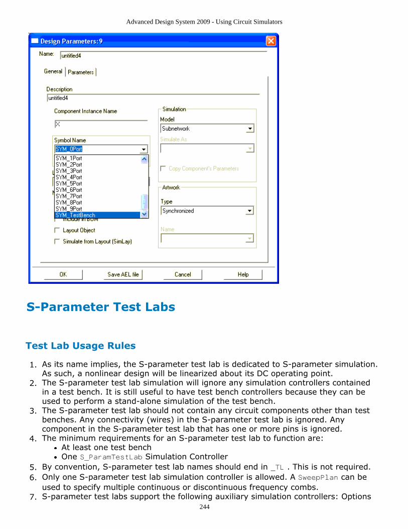
Advanced Design System 2009 - Using Circuit Simulators
244
S-Parameter Test Labs
Test Lab Usage Rules
As its name implies, the S-parameter test lab is dedicated to S-parameter simulation.1.As such, a nonlinear design will be linearized about its DC operating point.The S-parameter test lab simulation will ignore any simulation controllers contained2.in a test bench. It is still useful to have test bench controllers because they can beused to perform a stand-alone simulation of the test bench.The S-parameter test lab should not contain any circuit components other than test3.benches. Any connectivity (wires) in the S-parameter test lab is ignored. Anycomponent in the S-parameter test lab that has one or more pins is ignored.The minimum requirements for an S-parameter test lab to function are:4.
At least one test benchOne S_ParamTestLab Simulation Controller
By convention, S-parameter test lab names should end in _TL . This is not required.5.Only one S-parameter test lab simulation controller is allowed. A SweepPlan can be6.used to specify multiple continuous or discontinuous frequency combs.S-parameter test labs support the following auxiliary simulation controllers: Options7.

Advanced Design System 2009 - Using Circuit Simulators
245
Plan, Sweep Plan, Parameter Sweep, Optimization, Statistical, and DOE controllers.Variable equations (simulator expressions) and measurement expressions are8.supported. As with any top-level design, variables defined at the top are recognizedthroughout the hierarchy.Tuning is supported in the S-parameter test lab. Tuning within an S-parameter test9.lab works identically to tuning for a normal top-level design. Users can push into atest bench and select parameters or variables to tune. Users can also tune variablesand item parameters in the schematic window that displays the S-parameter test lab.Global nodes are supported, but they are not global across test benches. They are10.global within each test bench.Any global expression found in a test bench is available to all other test benches.11.The S_ParamTestLab controller has virtually the same user interface and displayed12.parameters as the standard S-Parameter controller.
Configuring an S-Parameter Test Lab
Determine the design files for which you want to calculate the S-parameters. You will1.create a test bench for each of these designs.Create the S-Parameter Test Lab.2.
Create a new schematic. This will be the test lab. It is recommended (but notrequired) that the name of the test lab schematic end in _TL . For this example,the name My_testlab_TL is used.
Schematic window with design named using _TL S-parameter test lab naming convention
In the S-parameter test lab schematic, change to the Simulation-S_Parampalette. Place an S_ParamTestLab controller (icon appears as SP Lab ). Configurethe S-parameter test lab controller the same way you would configure astandard S-parameter analysis.
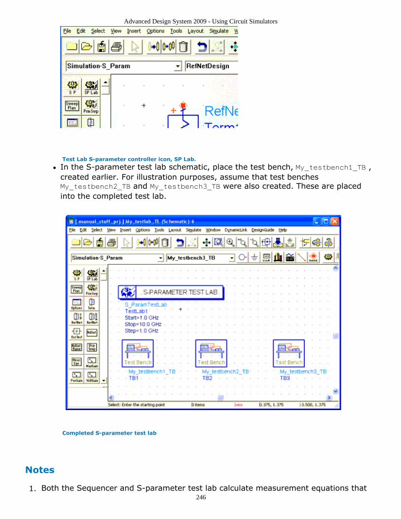
Advanced Design System 2009 - Using Circuit Simulators
246
Test Lab S-parameter controller icon, SP Lab.
In the S-parameter test lab schematic, place the test bench, My_testbench1_TB ,created earlier. For illustration purposes, assume that test benchesMy_testbench2_TB and My_testbench3_TB were also created. These are placedinto the completed test lab.
Completed S-parameter test lab
Notes
Both the Sequencer and S-parameter test lab calculate measurement equations that1.

Advanced Design System 2009 - Using Circuit Simulators
247
are contained in a test bench. The measurement equation is calculated only for thetest bench that contains it. The measurement equation should not use the test benchinstance id to refer to data (for example, S-parameters) that is generated for the testbench.If only one test bench is placed, the testbenchID prefix may be omitted. However,2.this is not recommended.
Data Display Naming Convention for Simulation Results
Standard Results Data
Standard S-parameter simulation output with Noise turned on produces the followingstandard output to the dataset:
S, S(i,j)
PortZ, PortZ(1), PortZ(2), PortZ(n), freq
Icor, Icor(i,j)
nf, nf(i), Nfmin
Rn, Sopt, te, te(n)
Where i = 1,2,... and j = 1,2,... are port indices.
An S-parameter test lab controller will also calculate these items. However, the test benchInstance ID will prefix the names. For example, an S-parameter test lab containing two,two-port test benches will produce the following results:
X1.S(1,1)
X1.S(2,1)
X1.S(1,2)
X1.S(2,2)
X2.S(1,1)
X2.S(2,1)
X2.S(1,2)
X2.S(2,2)
where X1 and X2 are the test bench instance ID names appearing in the test lab. If onlyone test bench appears in the S-parameter test lab, then the test bench prefix is notrequired.
Measurement Equation Results Data
Measurement equations appearing in the S-parameter test lab appear in the dataset as
MeasurementEquationName1
MeasurementEquationName2

Advanced Design System 2009 - Using Circuit Simulators
248
Measurement equations appearing in test benches in an S-parameter test lab will alsoappear in the dataset as
MeasurementEquationName1
MeasurementEquationName2
...
However, if the same measurement equation name appears in the S-parameter test laband a participating test bench, the following nomenclature is used
_Testlab1_TL_sp.MeasurementEquationName1
TestBench1_TB.MeasurementEquationName1
Optimization and Statistical Analysis
Configuring optimization and statistical analyses in an S-parameter test lab is similar toconfiguring them for a standard S-parameter analysis. An example project,TestLab_HOWTO_prj , is available in the ADS examples directory,$HPEESOF_DIR/examples/Tutorial .
This example illustrates optimization in an S-parameter test lab. The reader is advised toreview the example's Readme.dsn file, which contains detailed information.
Sequencer
Creating a Sequence
Create a test bench, then you are ready to specify the sequence. To do so, you'll need tocreate a new top-level design and instantiate each test bench in it. Next, you'll need toadd a Sequencer controller. This controller is available on the Simulation-Sequencingbitmap palette.

Advanced Design System 2009 - Using Circuit Simulators
249
Once you have instantiated the test benches and Sequencer controller, your top-leveldesign will look something like:
You are now ready to set the sequence, edit the Sequencer parameters and add each testbench in the desired order. When you first bring up the edit parameter box, you'll see theavailable test benches in the left pane.
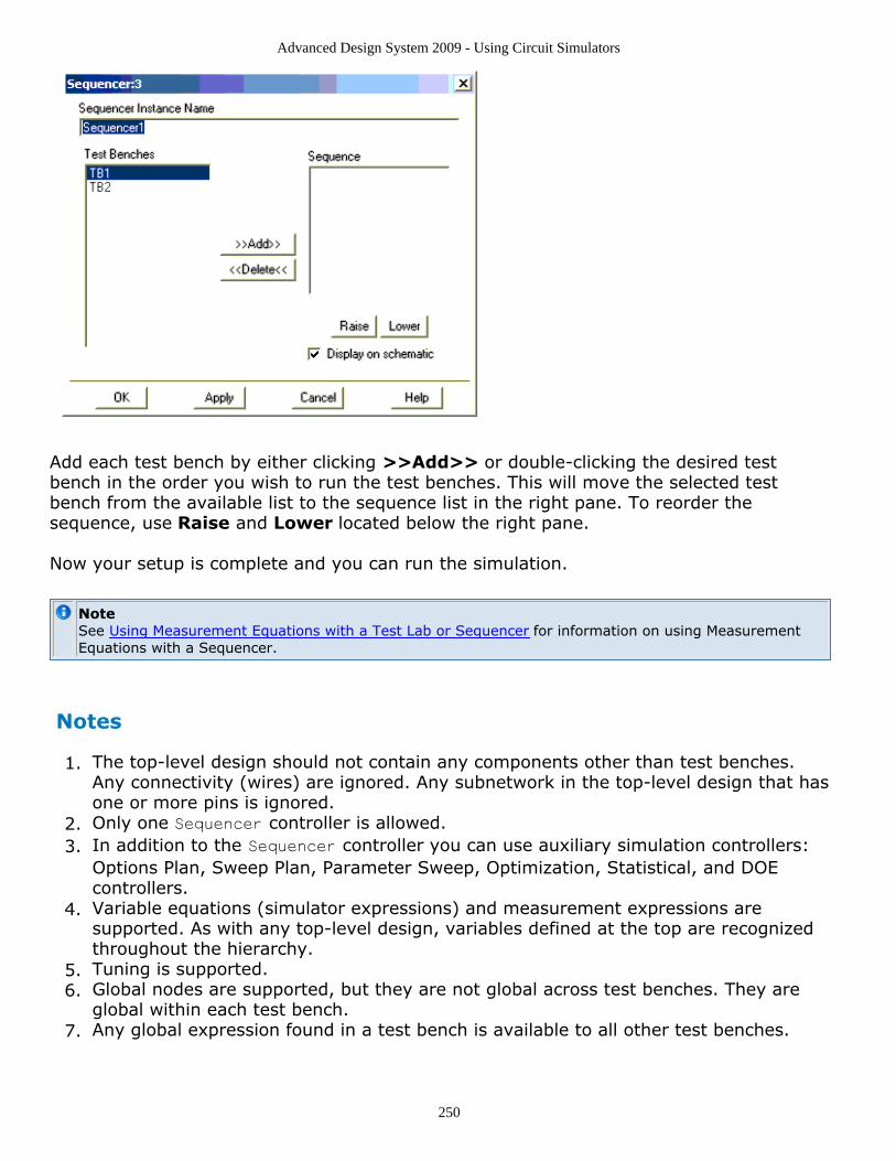
Advanced Design System 2009 - Using Circuit Simulators
250
Add each test bench by either clicking >>Add>> or double-clicking the desired testbench in the order you wish to run the test benches. This will move the selected testbench from the available list to the sequence list in the right pane. To reorder thesequence, use Raise and Lower located below the right pane.
Now your setup is complete and you can run the simulation.
NoteSee Using Measurement Equations with a Test Lab or Sequencer for information on using MeasurementEquations with a Sequencer.
Notes
The top-level design should not contain any components other than test benches.1.Any connectivity (wires) are ignored. Any subnetwork in the top-level design that hasone or more pins is ignored.Only one Sequencer controller is allowed.2.In addition to the Sequencer controller you can use auxiliary simulation controllers:3.Options Plan, Sweep Plan, Parameter Sweep, Optimization, Statistical, and DOEcontrollers.Variable equations (simulator expressions) and measurement expressions are4.supported. As with any top-level design, variables defined at the top are recognizedthroughout the hierarchy.Tuning is supported.5.Global nodes are supported, but they are not global across test benches. They are6.global within each test bench.Any global expression found in a test bench is available to all other test benches.7.

Advanced Design System 2009 - Using Circuit Simulators
251
Examples
For reference, a simple Ptolemy sequencer example is included in ADS.See /examples/Tutorial/Sequencer_prj documentation for more details.Additionally, BER connected solutions examples are also available on Microsoft Windows.See the following examples documentation located in the ADS Examples Documentation:
3GPP Uplink BER Receiver Characteristics TestWLAN 802.11a Receiver Input Level Sensitivity TestSimple Ptolemy Sequencer
Usage Rules
DSP cosimulation with A/RF is not supported.1.Test benches cannot refer to data saved in a dataset from a previous test bench. You2.can work around this limitation on the DSP schematic. See the simple example abovefor more details.A test bench cannot contain a Sequencer or S-parameter test lab controller.3.
Using Measurement Equations with a Test Lab orSequencer In either S-parameter Test Lab or Sequencer simulations, measurement equations areused in the same manner as they are in a standard analysis. However, because of thehierarchy associated with an S-parameter configuration, you need to specify the testbench instance ID when a measurement equation at the top-level refers to data generatedfor a test bench. The format is,
MeasEqnName = TestBenchInstanceID.Sij
where i=1,2,... and j=1,2,... are port indices.
The examples below illustrate this concept:
Example 1: Expressing S11 from test benches X1 and X2
S11_testbenchX1 = X1.S11
S11_testbenchX2 = X2.S11
Example 2: Utilizing S21 from test benches TB1 and TB2
S21_add = TB1.S21 + TB2.S21
S21_divide = TB1.S21/TB2.S21

Advanced Design System 2009 - Using Circuit Simulators
252
Example 3: Taking stability function for test benches TB1 and TB2
Stabfact_TB1=stab_fact(TB1.S)
Stabfact_TB2=stab_fact(TB2.S)
Improving Test Lab Simulation Efficiency Significant time performance gains in test lab simulation can be achieved by minimizingthe number of different test benches in the ADS test lab. Using the same test benchrepeatedly can result in faster test lab simulation. To take advantage of this, you musthave a situation requiring different versions of the same circuit.
To set up a test lab for improved simulation efficiency:
In the test circuit, place variables on the component parameters that define the1.different states.In the test circuit, create passed parameters using the variables created in step 1.2.Passed parameters are created by choosing File > Design Parameters and selectingthe Parameter Tab .Create a test bench containing the test circuit you created previously.3.In the test bench, create a set of passed parameters. Create one passed parameter4.in the test bench for each passed parameter created in the test circuit.Create a test lab. Make multiple placements of the test bench. With each placement,5.assign the passed parameters such that each passed parameter set defines the stateof each circuit to be tested.
Doing this, you are effectively placing the same test bench multiple times and eachplacement defines a different circuit state by the passed parameters used.

Advanced Design System 2009 - Using Circuit Simulators
253
RefNets
RefNet is short for " reference network". A RefNet is a component that is placed in adesign that enables the port impedance from another design file in the system (thereferenced network) to be referenced as a terminating impedance for the current designfile under test. There are two typical applications for RefNets:
Inter-stage circuit analysis and design: In some design applications it is desirable to1.simultaneously evaluate the performance of individual circuit stages terminated inthe input and output impedances of adjacent stages. For example, in transistormatching problem, the transistor in the S-parameter test lab can be terminated inthe output impedance of the input matching network and the input impedance ofoutput matching network. Further, it is desired that the matching networks beterminated looking into the appropriate side of the transistor. Simulation of thesenetworks simultaneously is accomplished with the S-parameter test lab, see S-Parameter Test Labs and Sequencer (cktsim) for more information. To accomplish thetermination of an individual stage referenced to a specific port of other stages in thedesign chain, the RefNet is utilized in the S-parameter test lab.The RefNet is intended to work only for its immediately preceding or succeedingstage with the additional requirement of that stage being in turn properly terminated.In designs containing several stages, proper termination must be used. In a multi-stage design where stage 1 contains the source, the 2nd stage input RefNet can pointto the stage 1 output impedance. However, the 3rd stage input RefNet cannot simplypoint to the stage 2 output impedance. Instead, another design must be createdcontaining stages 1 and 2, and the output impedance of this design must be used.Design specific termination: For some top level DC, AC, or S-Parameter design files,2.it may be desired to terminate a port whose impedance is characterized by data,from an external file (e.g. S-parameters, Z-parameters, Y-parameters) or some othernetwork.
There are two RefNet components that are available: RefNetTB and RefNetDesign . Bothof these components have the same functionality and are supported under DC, AC and S-Parameter analysis, with two differences:
RefNetTB supports nested network referencing while RefNetDesign does not. SeeRefNetTB Using an S-Parameter Test Lab for more information on using RefNetTB.RefNetTB uses a test bench as the reference design while RefNetDesign uses astandard (non-test-bench) schematic design. See RefNetDesign - File BasedTermination for more information on using RefNetDesign.
Note Nested referencing means that there is a top-level circuit under test that has one or more of its portsterminated with a RefNetTB . Further, the reference test bench (specified on the top-level RefNetTB )contains a RefNetTB , which again references other circuit designs in the system.

Advanced Design System 2009 - Using Circuit Simulators
254
RefNetTB and RefNetDesign
The parameters of RefNetTB are as follows:
Num The port number. This functions identically to the Num parameter found on the Termcomponent and power source components.
RefTestBenchName The name of the reference test bench (without the .dsn extension) that is used tocalculate the reference impedance for this termination.
RefPortNum Refers to the port number of the reference test bench. The referenced network, forexample, may contain several ports. This parameter identifies the port number (the Numparameter) of a termination in the reference test bench.
The parameters of the RefNetDesign component are as follows:
Num The port number. This functions identically to the Num parameter found on the Termcomponent and power source components.
RefDesignName The name of the reference design file (without the .dsn extension) that is used to calculatethe reference impedance for this termination.
RefPortNum Parameter that identifies a port number in the reference design. The reference impedance isthe impedance looking into this port of the reference design.
RefDesignZ Describes how all other ports, if any, in the referenced design are terminated. For the case ofa one-port referenced network, this parameter is not applicable and is ignored.
Notes:
The user cannot push into a RefNet component. If the user wants to view the1.reference design (test bench), this is accomplished by either toggling design files inthe current schematic window or opening a new schematic window and viewing thereference design file there.RefNet components do not support passed parameters.2.
RefNetTB Using an S-Parameter Test LabTo best explain this procedure, a tutorial approach will be used. The following example willbe considered:The narrow-band amplifier is partitioned out into three subnetworks: input.dsn,
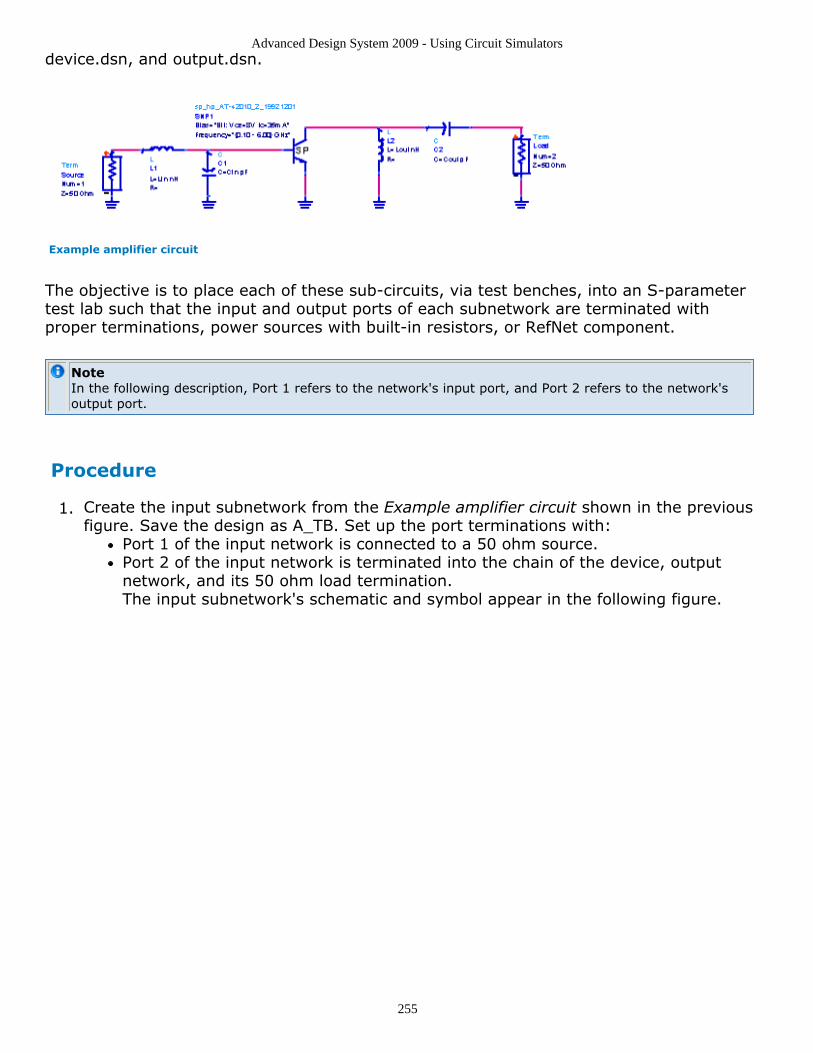
Advanced Design System 2009 - Using Circuit Simulators
255
device.dsn, and output.dsn.
Example amplifier circuit
The objective is to place each of these sub-circuits, via test benches, into an S-parametertest lab such that the input and output ports of each subnetwork are terminated withproper terminations, power sources with built-in resistors, or RefNet component.
NoteIn the following description, Port 1 refers to the network's input port, and Port 2 refers to the network'soutput port.
Procedure
Create the input subnetwork from the Example amplifier circuit shown in the previous1.figure. Save the design as A_TB. Set up the port terminations with:
Port 1 of the input network is connected to a 50 ohm source.Port 2 of the input network is terminated into the chain of the device, outputnetwork, and its 50 ohm load termination.The input subnetwork's schematic and symbol appear in the following figure.
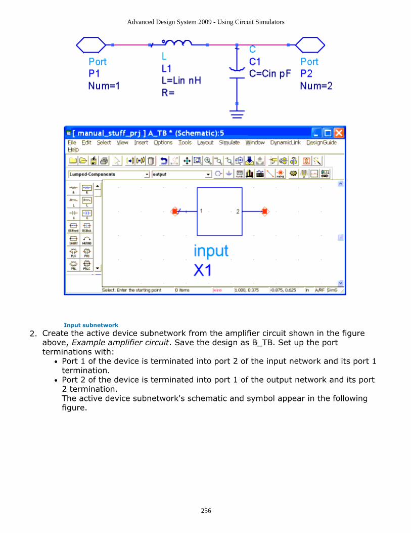
Advanced Design System 2009 - Using Circuit Simulators
256
Input subnetwork
Create the active device subnetwork from the amplifier circuit shown in the figure2.above, Example amplifier circuit. Save the design as B_TB. Set up the portterminations with:
Port 1 of the device is terminated into port 2 of the input network and its port 1termination.Port 2 of the device is terminated into port 1 of the output network and its port2 termination.The active device subnetwork's schematic and symbol appear in the followingfigure.

Advanced Design System 2009 - Using Circuit Simulators
257
Active device subnetwork
Create the output subnetwork from the amplifier circuit shown in the figure above,3.Example amplifier circuit. Save the design as C_TB. Set up the port terminationswith:Port 1 of the output network is terminated in the reverse chain from the deviceoutput, the input circuit, and its 50 ohm source termination.The output subnetwork's schematic and symbol appear in the following figure.
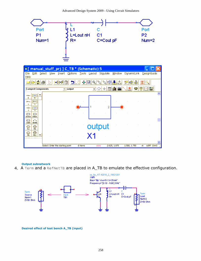
Advanced Design System 2009 - Using Circuit Simulators
258
Output subnetwork
A Term and a RefNetTB are placed in A_TB to emulate the effective configuration.4.
Desired effect of test bench A_TB (input)

Advanced Design System 2009 - Using Circuit Simulators
259
Test bench A_TB completed
Take note of the RefNetTB parameters as follows:
Num=2 Port 2 of the test bench
RefTestBenchName="B_TB" Points to the device test bench shown, which in forthcoming steps will beterminated with C_TB.
RefPortNum=1 The port number of B_TB where the impedance is taken.
Two RefNetTB components are placed in B_TB (device test bench) to emulate the5.effective configuration.
Desired effect of test bench B_TB (input) with Term and RefNetTB placed
Test bench B_TB completed
Take note of the RefNetTB s placed as follows:

Advanced Design System 2009 - Using Circuit Simulators
260
Term1 Parameters
Num=1 Port 1 of the test bench
RefTestBenchName="A_TB" Points to the input test bench.
RefPortNum=2 The port number of A_TB where the impedance is taken.
Term2 Parameters
Num=2 Port 2 of the test bench
RefTestBenchName="C_TB" Points to the output test bench.
RefPortNum=1 Port number of C_TB where the impedance is taken.
A RefNetTB and a Term are placed in C_TB (output test bench) to emulate the6.effective configuration.
Desired effect of test bench C_TB (output) with RefNetTB and Term placed
Test bench C_TB completed
Take note of the RefNetTB parameters as follows:

Advanced Design System 2009 - Using Circuit Simulators
261
Num=1 Port 1 of the test bench
RefTestBenchName="B_TB" Points to the device test bench shown in the figure above, Test bench B_TBcompleted which in is nested to A_TB via the test bench shown in the figureabove, Test bench A_TB completed.
RefPortNum=2 This is the port number of B_TB where the impedance is taken.
With test benches A_TB, B_TB, and C_TB, finished, the S-parameter test lab is7.created.
Completed S-parameter test lab incorporating RefNetTB
There is an optional step that may be desirable. The input, device, and output, can8.be placed into one test bench for viewing performance of the entire circuit chain.
Test bench for entire circuit chain

Advanced Design System 2009 - Using Circuit Simulators
262
S-parameter test lab incorporating sub-circuit and entire circuit, ABC_TB, test benches
RefNetDesign - File Based TerminationThe steps to create a file-based termination are as follows:
Create a sub-circuit that reads in data file. For this example, a one-port s-parameter1.file is used.Save the design file from step 1 as read_term_data.dsn .2.
Top-level one-port design file to read in S-parameter data file

Advanced Design System 2009 - Using Circuit Simulators
263
In a design file that contains the circuit under test, place RefNetDesign at the pin3.where the S-parameter-based termination is to be applied.
Top-level design that references a file-based one-port network to realize a file-based termination
The parameters of RefNetDesign were assigned as follows:
Num=1 Port number for the top level design.
RefDesignName="read_term_data" Name of the design file for the reference network.
RefPortNum=1 Port number where the impedance is taken for the reference network.Since the reference network is a one-port, this is set to 1.
RefDesignZ=50 For this example, this parameter is not applicable. Had port componentsbeen placed in the reference design, this parameter instructs how thoseports are to be terminated.

Advanced Design System 2009 - Using Circuit Simulators
264
An ADS Simulation ExampleThis topic is a detailed simulation example for ADS. The circuit is a simple BJT and thesimulation is set up to calculate the DC operating point. The simulation process isdescribed here in detail, and this process can be applied to more complex circuits andsimulations.
Before continuing with this topic, you should be familiar with the other topics in UsingCircuit Simulators (cktsim), in Schematic Capture and Layout (usrguide), and in theAdvanced Design System Quick Start (adstour).
The DC_OP_POINT.dsn design used here is located in the Examples directory underMW_Ckts/LNA_prj . Details on working with example projects can be found in SchematicCapture and Layout (usrguide).
Working through this example consists of these tasks:
Placing Circuit SourcesSpecifying Points for Collecting DataSelecting a Simulation TypeSelecting a Sweep Type and PlanSetting Simulation OptionsModifying the Simulation SetupStarting the SimulationDisplaying Simulation Data
Placing Circuit SourcesIn many cases your circuit will contain sources. In this example, you need to select avoltage source that is appropriate for a DC simulation:

Advanced Design System 2009 - Using Circuit Simulators
265
From the Component Palette List, choose Sources-Time Domain .1.Select V_DC ( DC Voltage Source) and place this component in the Schematic2.window.Set the DC voltage (Vdc) to 3.0 V .3.
Ensuring Sources are Connected Properly
You must ensure that the sources are connected properly to the circuit. You can do thistwo ways:
Wire the source directly to your circuit.Use node names ( Insert > Wire/Pin Label ) to define connections. By labeling theend of the source and a point in the circuit, the source then behaves as if connectedphysically to that point of the circuit. For example, named connections can be usedfor Vcc, Vb, and Ve.
If you are wiring components, the color of the pin changes when a successful connectionis established. Wires that are simply overlaid on intervening nodes will not be connectedto those nodes, and clicking on the intervening nodes after the end node is wired does notensure that the intervening nodes are connected properly.
In addition, the endpoints of dangling wires (wires that are connected at one end only)can be moved but not edited. To move an endpoint, choose Edit > Move > Move WireEndpoint . When crosshairs appear, select the open endpoint and move it; the wire willmove with it. It is also possible, using standard copy and move commands, to move andcopy dangling wires and networks of wires.
To label and share a source:
Choose Insert > Wire/Pin Label and a dialog box appears.1.Enter a name for the node (for example, Vcc).2.Click the pin of the source you want to label (for example, the positive side of V_DC).3.The label Vcc appears at that node.Next click the pin of a node to which you want Vcc to apply (for example, one end of4.a resistor). The resistor node is also labeled Vcc. (Note that you must click thecomponent pin, not a wire between components.)
Note To delete a named connection, choose Edit > Wire/Pin Label > Remove Wire/Pin Label. Whencrosshairs appear, click the pin whose connection name you want to remove.
Edit any parameters of the source as needed.5.
Specifying Points for Collecting Data You must specify the points in the circuit where voltage and current values will becollected and saved in the dataset:

Advanced Design System 2009 - Using Circuit Simulators
266
To identify points where you want voltages to be taken, use node names ( Insert >Wire/Pin Label ) or global nodes ( Insert > Global Node ). For circuit nodes that arelabeled this way, voltages will be calculated during the simulation and saved to thedataset.For collecting current values, insert current probes (I_Probe) in your circuit at pointsof interest. Current probes are found on the Probe Components palette.Some components, such as the DC voltage source (V_DC) used in this example,include a SaveCurrent parameter. If this is set to yes , the current flowing throughthis component will be saved to the data set.
To help identify the data collected by a probe or source, you might want to change thedefault Instance Name to something more meaningful. For example, you can name a DCvoltage source Vsupply. The current through that source will appear in the dataset asVsupply.i .
NoteCurrent probes (I_Probe components) must be placed so that the arrow on the probe points in thedirection of (positive) current flow. To flip a probe horizontally, choose Edit > Rotate/Mirror > Mirror AboutY .
In general, voltage and current data is in phasor representation, so the voltage values at named nodes arepeak voltage.
The process for labeling nodes is described in Ensuring Sources are Connected Properly.
To insert a current probe:
Select the Probe Components palette.1.Select the I_Probe component and place it at the desired point in your schematic.2.(You may need to move components or rewire to do this.) Edit the probe componentand change the Instance Name to something that suggests its purpose in the circuit.
For details on selectively sending data to the dataset, refer to Selectively Saving andControlling Simulation Data (cktsim).
Selecting a Simulation TypeThere are a variety of simulation methods to choose from. To use a particular simulator,you must have purchased a license for it. If you do not have a license, a message willappear when you attempt to run the simulator. This may also happen if you share licensesthat are already in use.
Each simulator has its own palette, which can be selected from the Component Palette

Advanced Design System 2009 - Using Circuit Simulators
267
List. Details for using each simulator are described in later topics.
To add a DC simulation component (for this example):
Select the Simulation-DC palette.1.Select and place the DC component on your schematic.2.
Editing Simulation Parameters
There are two ways to edit simulation parameters:
You can edit parameters directly on the schematic. Click somewhere within theparameter value to invoke the on-screen editor, and change the value as desired.Press Return to enter data and go to the next entry. Note that by default, not allparameters are displayed on the schematic; to view/edit additional parameters, usethe dialog box, as described next.You can edit parameters within the dialog box. To open the dialog box, either double-click the simulation component, or select it and choose Edit > Component > EditComponent Parameters . You can also bring up the dialog box using the Edit
Component Parameters icon on the toolbar.
NoteFor many simulation options, the default parameters should provide satisfactory results and will not needediting.

Advanced Design System 2009 - Using Circuit Simulators
268
You may find it useful to display (on the schematic) the options you have selected, toremind you of the parameters governing a simulation.
To display additional parameters on the schematic:
Select the Display tab.1.Select each parameter you want to appear and click OK.2.
To exercise certain simulation options, you must first display them on the schematic, thenset them equal to the desired value. For example, to send a defined power parameterRF_power to the dataset following a simulation, use the Output tab of the DC OperatingPoint dialog box. Refer to the section Selectively Saving and Controlling Simulation Data(cktsim).
Selecting a Sweep Type and Plan The Sweep tab enables you to identify the parameter that you want to sweep, and thenspecify the sweep type. You can sweep over:
A single pointA linear rangeA logarithmic range
After you select the sweep type, you can then specify the sweep range.
You can also select a sweep plan . A sweep plan enables you to specify a sweep once andthen use these settings in other places. For more information, refer to Parameter Sweepsand Sweep Plans (cktsim). Note that for some simulators, these settings are found on theFreq tab.
To set the sweep values for this example:
Double-click the DC component to edit it.1.Set the following parameters as shown here:2.
Parameter to sweep = VBEStart = 0.6Stop = 0.85Step size = .002Num. of pts. = 126
If using the Load Sharing Facility (LSF) utility, you can break up a sweep and run thesimulation on multiple machines, in parallel, by selecting Parallel Hosts as the SimulationMode ( Simulate > Simulation Setup ). Individual sweep points are run on each machineand results combined into a single dataset on the local machine. For details on setting upremote and local machines for remote processing, see the topic Using Remote Simulationin the installation documentation for your platform.

Advanced Design System 2009 - Using Circuit Simulators
269
Setting Simulation OptionsAn Options component can be used with any simulation. The most common use of theOptions component is to set the simulation temperature, but it also enables you to specifysettings for convergence tolerances, warnings and other advanced options. (For thisexample, an Options component is not used.)
To add an Options component:
Select any simulation palette.1.Select and place a simulation Options component and double-click to edit it. You can2.set general simulation options such as temperature, DC convergence tolerances,warnings, and other settings.
For more information about each field, click the Help button at the bottom of the OptionsComponent dialog box.
Modifying the Simulation SetupAdditional simulation setup options include:
Specifying a name for the dataset to which simulation data will be savedAutomatically displaying data when the simulation is finishedSelecting a different machine on which to run the simulation
To specify simulation setup options:
From the Schematic window, choose Simulate > Setup . A Simulation Setup dialog1.box appears:
The data calculated during a simulation is saved in a dataset. The default dataset2.name is the same as the project. Change the name as desired.By default, the Data Display will automatically launch when the simulation is3.complete. If the simulation results were displayed before, the same window will openif you specify its name in the Data Display field.If you use remote simulation hosts, you can specify a machine other than the local4.one for running the simulation. For more information on how to set up remote

Advanced Design System 2009 - Using Circuit Simulators
270
machines, see the installation documentation for your platform.
Starting the SimulationThere are several ways to launch a simulation:
Press F7 on the keyboard.Click the Simulate icon on the toolbar.Choose Simulate > Simulate from the Schematic window.Choose Simulate from the Setup dialog box while it is open.
When the simulation begins, a status and error message window appears. When thesimulation is complete, the line Simulation finished . at the bottom of the windowindicates that the simulation has run successfully. The location of the dataset where thesimulation data is saved is also noted.
Displaying Simulation Data You will typically want to view most of your results in a Data Display, however you alsohave the option to view DC results on the schematic and view lists of device operatingpoint details. While it is not very useful in this example-given that the DC results arereported only for the last point in a sweep – it illustrates an important feature.
Viewing the DC Solution
Choose Simulate > Annotate DC Solution . DC voltages and currents appear at1.the pins of all the active devices and lumped elements, as shown below.
NoteCurrent is defined as positive if flowing into a device, so +13.5 mA is flowing from the emitter toground.

Advanced Design System 2009 - Using Circuit Simulators
271
NoteTo clear the annotations, choose Simulate > Clear DC Annotation from the main menu. You willhave to resimulate to annotate again.
Viewing the Detailed Device Operating Point
In the same Schematic window, choose Simulate > Detailed Device Operating1.Point . Crosshairs appear.Place the crosshairs over a transistor and click. A detailed DC operating point listing2.appears.As you select other devices in a circuit, the DC operating point data for additional3.devices is added to the list.
For more information about the parameters that are displayed in the list, refer to thedocumentation for the specified component.

Advanced Design System 2009 - Using Circuit Simulators
272
Viewing the Brief Device Operating Point
To view a subset of the above information that covers the most common parameters,choose Simulate > Brief Device Operating Point and select a device. The details are similarto those in the detailed list, but this list contains fewer parameters.
For details about the data that appears in the list, refer to the selected component'sdocumentation.
Viewing More Results in the Data Display
The remainder of the simulations results can be viewed using the Data Display. Forcomplete details on how to use the Data Display, refer to Data Display (data) and to theAdvanced Design System Quick Start (adstour). The results of this simulation are inDC_op_point.dds. In this example, collector current versus Vbe at Probe1 is displayed.

Advanced Design System 2009 - Using Circuit Simulators
273
There are various options for plotting and scaling data. To edit general plot characteristics,select the Plot Options tab. This allows you to enter a title and axis label. It also allowsyou to deselect Auto Scale and enter a scale that zooms in on a range of interest. You canalso choose between linear and log scales here, and select grid characteristics.
To edit a trace before placing it (unless you have selected the List plot type), select theparameter under Traces, then click Trace Options . Select the Trace Type , Trace Options ,and Trace Expressions tabs to select, for example, trace patterns, trace colors, and fontsfor labels, as well as to edit mathematical expressions for display.