university of nairobieie.uonbi.ac.ke/sites/default/files/cae/engineering/eie/design a... ·...
TRANSCRIPT

UNIVERSITY OF NAIROBI
SCHOOL OF ENGINEERING
DEPARTMENT OF ELECTRICAL AND INFORMATION ENGINEERING
DESIGN A THREE PHASE CONTROLLED RECTIFIER FOR USE IN THE
LABORATORY
PROJECT INDEX: 116
SUBMITTED BY
MWONGA BRIAN MATOLO
F17/39946/2011
SUPERVISOR: MR. S. L. OGABA
EXAMINER: MR OMBURA
PROJECT REPORT SUBMITTED IN PARTIAL FULFILLMENT OF THE
REQUIREMENT FOR THE AWARD OF THE DEGREE
OF
BACHELOR OF SCIENCE IN ELECTRICAL AND ELECTRONIC ENGINEERING OF
THE
UNIVERSITY OF NAIROBI
DATE SUBMITTED: 17TH MAY 2016

ii
DECLARATION OF ORIGINALITY
NAME OF STUDENT: MWONGA BRIAN MATOLO
REGISTRATION NUMBER: F17/39946/2011
COLLEGE: Architecture and Engineering
FACULTY/SCHOOL/INSTITUTE: Engineering
DEPARTMENT: Electrical and Information Engineering
COURSE NAME: Bachelor of Science in Electrical and Electronic Engineering
TITLE OF WORK: Three Phase Controlled Rectifier For Use In The Laboratory
1) I understand what plagiarism is and I am aware of the university policy in this regard
2) I declare that this final year project report is my original work and has not been submitted
elsewhere for examination, award of a degree or publication. Where other people’s work or my
own work has been used, this has properly been acknowledged and referenced in accordance
with the University of Nairobi’s requirements.
3) I have not sought or used the services of any professional agencies to produce this work.
4) I have not allowed, and shall not allow anyone to copy my work with the intention of passing
it off as his/her own work.
5) I understand that any false claim in respect of this work shall result in disciplinary action,
in accordance with University anti-plagiarism policy.
Signature…………………………………………………………………..
Date………………………………………………………………………..

iii
CERTIFICATION
The report has been submitted to the Department of Electrical and Information Engineering,
University of Nairobi with my approval as supervisor:
Mr. S. L. Ogaba.
Date: ……………………………..

i
DEDICATION
I dedicate this project to my parents and family for always believing in me and to my friends
for their encouragement and support.

ii
ACKNOWLEDGEMENT
I wish to appreciate the Almighty God for His amazing grace throughout my life. His love and
guidance has brought me this far to complete my final year project entitled “Three phase
controlled rectifier for use in the lab”.
I would also like to take this opportunity to thank all the people who had assisted me directly
and indirectly in completing the project. My first gratitude goes to Mr. S.L Ogaba my
supervisor for the project whom had given support, advice and Guidance. I am indebted to him
for always being there to help me shape the problem and provide insights towards the solution.
The progress I have made now would have been impossible without his guidance. I also
appreciate the teaching staff and non-teaching staff at the University of Nairobi, Department
of Electrical and Information Engineering for their selfless effort that enabled me to achieve
my academic goals during the entire course of my studies.
I would also like to thank my friends for their constant encouragement and helpful discussions
throughout the course of this work.
Last but not least, I would like to thank my beloved parents who had given me a lot of moral
support while I was doing this project.
Once again to all, thank you very much.

iii
ABSTRACT
Three phase AC to DC conversion of electric power is widely employed in adjustable speed
drives (ASDs), uninterruptible power supply (UPSs), HVDC systems and utility interfaces with
non-conventional energy sources such as electroplating welding units etc, battery charging for
electric vehicles and power supplies for telecommunication systems.
The purpose of this project is to successfully convert three phase ac to dc conversion of electric
power using SCRs. AC to DC line commutated converters are used as the most usual choice
for application. This is due to simplicity of the circuits requiring a minimum number of active
and passive components. Thyristors or SCRs are the main line commutated power switches. In
this project is built on thyristors and a control or firing system using ATmega328p
microcontroller which is used to trigger the three phase full-controlled bridge rectifier.it adopts
three synchronization signals; 6-channels trigger pulses from it are very
symmetrical and the pulses can be shifted within a cycle of a sine wave from 0 degree to 162
degrees
Its structure of this circuit is simple and consists of the rectifier circuit consisting of the 6-SCRs
and the isolation circuit with the protection system, a microcontroller a LCD screen
,synchronization circuits and the control voltage circuit.; its performance is high stable and
reliable; Its anti-interference ability is strong and its operation is easy.
A zero crossing circuit attached to the AC lines produces a digital signal to the processor (based on
signal zero crossings) that is captured and used to predict the next zero crossing capture time
and fire the SCR’s based on this prediction. For accuracy and precision, a phase locked loop
algorithm is implemented in software that works to improve the accuracy of the next predicted
zero crossing and locks to produce the desired output voltage.

iv
Table of Contents
DECLARATION OF ORIGINALITY ............................................................................................... ii
CERTIFICATION ............................................................................................................................... iii
DEDICATION........................................................................................................................................ i
ABSTRACT .......................................................................................................................................... iii
LIST OF ABBREVIATIONS ............................................................................................................... vii
CHAPTER 1 .......................................................................................................................................... 1
1.1 Overview .......................................................................................................................................... 1
1.2 background .................................................................................................................................. 3
1.3 Objectives..................................................................................................................................... 4
1.4 Scope ............................................................................................................................................ 4
1.5 problem statement ...................................................................................................................... 4
1.6 Project Report outline ................................................................................................................ 5
CHAPTER 2 .......................................................................................................................................... 6
LITERATURE REVIEW .................................................................................................................... 6
2.1 Introduction ................................................................................................................................. 6
2.2 Theory of rectifiers ..................................................................................................................... 7
2.2.1 Single-Phase Rectifiers ...................................................................................................... 10
2.2.2 Three Phase Rectifiers ....................................................................................................... 13
2.3 Thyristor commutation — effect of the AC input reactance ................................................ 18
2.4 Power displacement factor and Power factor ................................................................... 21
2.5 Effects on the AC mains voltage .............................................................................................. 22
2.6 How to reduce the harmonics on the AC mains ................................................................... 23
2.6.1 Three-Phase Line Reactors ............................................................................................. 23
2.6.2 DC-Link Choke .................................................................................................................... 24
2.6.3 Passive Filters ..................................................................................................................... 24
2.7 Silicon Controlled Rectifier ...................................................................................................... 26
2.7.1 Working of SCR ................................................................................................................. 27
2.7.2 Switching Characteristics of SCR..................................................................................... 28
2.7.3 SCR Ratings ....................................................................................................................... 29
2.7.4 Gate Circuit Requirements. .................................................................................................. 29
2.7.5 SCR protection ................................................................................................................... 31
2.8 Previous researches ...................................................................... Error! Bookmark not defined.
CHAPTER 3 ........................................................................................................................................ 32
METHODOLOGY ............................................................................................................................. 33
3.1 introduction ............................................................................................................................... 33

v
3.2 Design ......................................................................................................................................... 34
3.2.1 Input .................................................................................................................................... 34
3.2.2 The rectifier circuit ............................................................................................................ 35
3.2.3 Synchronization circuit/ Zero crossing detector circuits. ............................................... 38
3.3.3 Controlling voltage ............................................................................................................. 39
3.3.4 Generating of the firing pulses .......................................................................................... 40
3.4 Software Design ......................................................................................................................... 43
3.4.1 Main Program .................................................................................................................... 43
3.4.2 ADC program for delay ..................................................................................................... 45
CHAPTER 4: ....................................................................................................................................... 46
RESULTS AND ANALYSIS ............................................................................................................. 46
4.1 Theoretical Results .................................................................................................................... 46
CHAPTER 5 ........................................................................................................................................ 47
CONCLUSION AND RECOMMENDATION ............................................................................ 47
5.1 Conclusion .................................................................................................................................. 47
5.2 Recommendations for Further Work ..................................................................................... 47
REFFERENCES ................................................................................................................................... 48

vi
TABLE OF FIGURES
Figure 1: Rectifier ................................................................................................................................... 2
Figure 2: inverter..................................................................................................................................... 2
Figure 3: Chopper ................................................................................................................................... 2
Figure 4 cycloconverter ........................................................................................................................... 3
Figure 5 :power electronics interface between the power processor and controller ............................ 4
Figure 6:uncontrolled rectifier and sub divisions ................................................................................... 8
Figure 7 : controlled rectifier and sub divisions ...................................................................................... 9
Figure 8: Single-phase half wave diode rectifier-R/L Load ................................................................... 10
Figure 9: A basic half wave controlled rectifier .................................................................................... 11
Figure10 a: The Bridge Rectifier Figure 10 b: single diode rectifier waveforms ............................. 11
Figure 11: a full wave controlled bridge rectifier .................................................................................. 12
Figure 12: single way rectifier ............................................................................................................... 13
Figure 13: waveforms for the number of pulses of single way rectifier ............................................... 14
Figure 14: Three - phase bridge rectifier (a) and (b) it’s ideal equivalent circuit ................................. 14
Figure 15(a): source and output voltage............................................................................................... 15
Figure 16 b: waveforms of voltages and current of a three phase rectifier operating in the constant
load current mode ................................................................................................................................ 15
Figure 17: (a) fully-controlled three phase bridge ciruit, (b) the output voltage waveforms with small
fring angle and (c) with large firing angle ............................................................................................. 18
Figure 18: Commutation of thyristor from one phase to another ....................................................... 19
Figure 19: Effect of the overlap angle on the voltage and currents ..................................................... 20
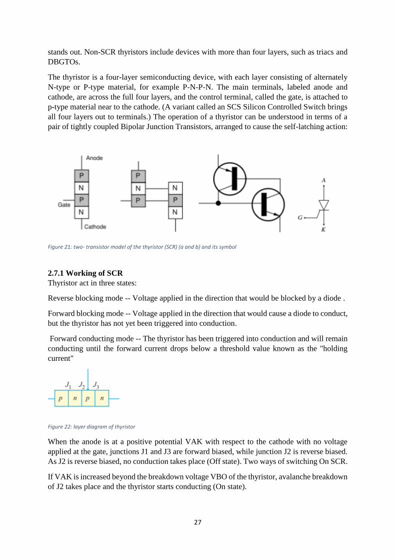
Figure 20: two- transistor model of the thyristor (SCR) (a and b) and its symbol ................................ 27
Figure 21: layer diagram of thyristor .................................................................................................... 27
Figure 22: The static V-I characteristic of an SCR.................................................................................. 28
Figure 23: (a) Firing network desirable network connection,(b) firing network load line ................... 30
Figure 24: Three phase controlled rectifier circuits .............................................................................. 33
Figure 25: Tri-phase control rectifier block diagram ............................................................................ 34
Figure 26: The input circuit to rectifier ................................................................................................. 35
Figure 27: three phase connected to the supply with the snubber circuits and isolation circuit ........ 36
Figure 28: MOC3021 isolator connection to SCR and interface with ATmega328p microcontroller ... 37
Figure 29: zero crossing circuit with input transformer ....................................................................... 38
Figure 30: square wave zero crossing signals of the two phases ......................................................... 39
Figure 31: Controlling Voltage circuit ................................................................................................... 40
Figure 32: MCU and LCD display ........................................................................................................... 43
Figure 33: waveform of the output pulse ............................................................................................. 43
Figure 34: flow chart ADC subroutine and delay control ..................................................................... 45

vii
LIST OF ABBREVIATIONS
AC - Alternate Current
DC - Direct Current
SCR - Silicon Control Rectifier
BJT – Bipolar junction transistors
GTO - Gate Turn-Off Thyristors
VCD - Variable speed drive
THDI - Total Harmonic Distortion Current
MOSFET - Metal–Oxide–Semiconductor Field-Effect Transistor
HPF - High Power Factor
ADC – Analog Digital Converter
IC - Integrated Circuit
RF - Ripple Factor
TUF- Transformer Utilization Factor
ISR -interrupt service routine
PCINT- Pin change interrupt
MCU-Microcontroller
LCD-Liquid Crystal Display

1
CHAPTER 1
INTRODUCTION
1.1 Overview
Power electronics refers to control and conversion of electrical power by power
semiconductor devices wherein these devices operate as switches Power electronics
circuits convert electric power from one form to another using electronic devices.
Power electronics circuits function by using semiconductor devices as switches, thereby
controlling or modifying a voltage or current. [3]
Power electronics started with the development of the mercury arc rectifier. Invented
by peter cooper 1902, it was used to convert alternating current (AC) into direct current
(DC).From the 1920’s on Uno Lamm developed a mercury valve with grading
electrodes making them suitable for high voltage direct current power transmission. .
By late 1940 Shockley's invention of the bipolar junction transistor (BJT) improved the
stability and performance of transistors, and reduced costs and higher power
semiconductor diodes became available and started replacing vacuum tubes.
The invention of the integrated circuit(IC) by J.Kibly from “Texas Instruments” in
1958 followed by the planar process of “Fairchild Semiconductor” in 1959 that became
the key solid state electronics. The period of power semiconductors began in 1956,
when the silicon controlled rectifier (SCR) was invented by General Electric, greatly
increasing the range of power electronics applications.
The introduction of SCRs resulted into significant improvements in
semiconductor fabrication technology and physical operation were made and many
different types of power semiconductor devices appeared. The growth in power
electronics in the last 15 years application has been remarkable because of this
introduction of very fast and high-power switching devices, like the metal-oxide
semiconductor field-effect transistors (MOSFET), bipolar NPN and PNP transistors,
junction transistors and gate turn-off (GTO) thyristors were developed. Later the
microprocessors, specified integral circuits and power integral circuits were produced.
In the last 20 years, the growth in power electronics application has been
remarkable because of this introduction of very fast and high-power switching devices,
coupled with the utilization of state-of –the –art control algorithms. An electric power
can be converted from one form to another form by using power electronics devices
.The function of power electronics circuits by using semiconductor devices as switch is
modifying or controlling a voltage. The goal of power electronics circuits are to convert
electrical energy from one form to another, from source to load with highest efficiency,
high availability and high reliability with the lowest cost, smallest size and weight and
are hence called converters. They serve as interface between source and load.
Converters are classified by the relationship between input and output.

2
Figure 1: Rectifier
AC to DC converters- Rectifiers that transform ac to DC with adjustment of voltage and current
Figure 2: inverter
DC to AC converters- inverters that produce AC of controllable magnitude and frequency,
particularly with galvanic isolation via a transformer
Figure 3: Chopper
DC to DC converters -conversion of an unregulated dc voltage to a regulated dc voltage, linear
regulators and switching choppers.

3
Figure 4 cycloconverter
AC to AC converters-conversion of an AC power source from one amplitude and frequency
to another amplitude and frequency
1.2 background
Power electronic converters can be found wherever there is a need to modify a form of electrical
energy (i.e. change its voltage, current or frequency). The power range of these converters is
from some milliwatts (as in a mobile phone) to hundreds of megawatts (e.g. in a HVDC
transmission system). With classical electronics, electrical currents and voltage are used to
carry information, whereas with power electronics, they carry power. Thus, the main metric of
power electronics becomes the efficiency. The first very high power electronic devices were
mercury arc valves. In modern systems the conversion is performed with semiconductor
switching devices such as diodes, thyristors and transistors. In contrast to electronic systems
concerned with transmission and processing of signals and data, in power electronics
substantial amounts of electrical energy are processed. An AC/DC converter (rectifier) is the
most typical power electronics device found in many consumer electronic devices, e.g.
television sets, personal computers, battery chargers, etc. The power range is typically from
tens of watts to several hundred watts. In industry the most common application is the variable
speed drive (VSD) that is used to control an induction motor. The power range of VSDs start
from a few hundred watts and end at tens of megawatts. Power electronics refers to control and
conversion of electrical power by power semiconductor devices wherein these devices operate
as switches. Advent of silicon-controlled rectifiers, abbreviated as SCRs, led to the
development of a new area of application called the power electronics. Prior to the introduction
of SCRs, mercury-arc rectifiers were used for controlling electrical power, but such rectifier
circuits were part of industrial electronics and the scope for applications of mercury arc
rectifiers was limited. Once the SCRs were available, the application area spread too many
fields such as drives, power supplies, aviation electronics, high frequency inverters and power
electronics originated.

4
Figure 5 :power electronics interface between the power processor and controller
1.3 Objectives
The first objective of this project is to design a three phase controlled rectifier circuit to
convert three phase 110V AC input voltage to DC output voltage.
The second objective is to develop a hardware of three phase controlled rectifier with line
input voltage of 110v using six SCRs to convert AC input to a DC output depending on
the firing angle of the SCRs and a control circuit for firing angle to range between 0 ̊ to
160 ̊ degrees varying the DC output voltage and can be used by students in the lab to study.
1.4 Scope
This project concentrates on design of circuit and development of hardware to get a DC output
at a three phase AC input. The three phase controlled rectifier uses six SCRs with protective
circuits and filter circuits in the rectifier circuit and AVR Atmega328p microcontroller and a
synchronizing circuit (zero crossing detector circuit) in the control circuit. Besides the scope is
to program a microcontroller to control delay angle alpha 0 ̊ to 160 ̊ to rectifier AC voltage DC
voltage.
To develop the whole project, it consists of three methods which are the concept of switching,
electrical structure, and the software programming.
After designing and building completely the rectifier circuit, the driver circuit should be able
to control the delay angle α. The delay angle will be adjusted by using microcontroller AVR
Atmega328p. It will involve the programming development to control the ON state of the SCRs
and adjust the phase angle. Here, the trigger angle of SCRs will be programmed in certain time
sequence to ensure the input voltage goes from low to full voltage on which the circuit is to be
connected to different loads or supply dc voltage.
1.5 problem statement
A rectifier is a power electronic circuit converter that converts bidirectional AC voltage
to unidirectional DC voltage by using power diodes or by controlling the firing angle of

5
thyristors or controllable switches. Rectification is of two forms uncontrolled rectification
where there is use of power diodes and controlled rectification by use of thyristors or
controllable switches.it can be either single phase or three phase and this depends on the
input. A diode is the simplest electronic switch. It is uncontrollable in that the on and off
conditions are determined by voltages and currents in the circuit. The diode is forward-
biased (on) and reverse-biased (off).
AC to DC converter is mostly used in industries and also in domestic equipment.ac
voltage from generators are variable hence provide variable dc if uncontrolled AC-DC
converter is used, this variable DC is not suitable to be used in the lab for voltage supply
purposes .
To overcome this problem the output of the voltage of the rectifier need to be controlled.
In the design of the three phase rectifier thyristors or SCRs (Silicon Control Rectifier) are
connected in full wave rectifier. Thyristors are electronic switches used in power electronic
circuits where control of switch turn-on is required and controlled by a control system for
which the output voltage can be varied by the user to desired voltage.
Power converter system was designed using modern technology and methods to implement a three
phase fully-controlled rectifier.
1.6 Project Report outline
This project report is structured into five chapters and every chapter elaborates into details
more about this chapter.
Chapter one is the introduction of this project which gives the overview of this project.
Converters of power by providing background information. The three phase controlled rectifier
ac to dc converter is discussed including the objectives, scope and problem statement as a guide
to develop the three phase controlled rectifier.
The second chapter is composed of the literature review of the three phase controlled rectifier.it
discusses the previous research done by others and the comparison with the relevance the
research. Discussion of the books and papers that are used in the reference and the shortcomings
of the previous research.
Chapter three explains and discusses on the methodologies of the three phase controlled
rectifier that has been used and applied in the design and development of the hardware.it also
consists of block diagram, flow charts and circuit diagrams which are explain the process of
implementation and how the three phase AC voltage converts to DC voltage then connected to
the different loads.it also discusses how the outputs voltage can be varied.
The fourth chapter is discussing and displaying all the results obtained, the analysis of the
results and the limitations encountered in the project.
Chapter five will discuss on the conclusion and summary of the development of the three phase
controlled rectifier project. In this chapter also discusses on the recommendation for this project
development or modification.
6
CHAPTER 2
LITERATURE REVIEW
2.1 Introduction
This chapter presents an overview of rectifier, the projects that have been made from various
sources like journals, books, articles and others. From the literature review the input that has
been collected is useful for better understanding of this project. It is because for nearly a
century, rectifier circuits have been the most common power electronics circuits used to convert
AC to DC. The AC-DC converter produces a DC output from an AC input while the average
power transferred from an AC source to a DC load.
A rectifier is an electrical device that converts alternating current (AC), which periodically
reverses direction to direct current (DC). The word rectification is used not because these
circuits produce DC but rather because the current flows in one direction. Rectifiers have many
uses including as components of power supplies and as detectors of radio signals. Rectifiers
may be made of solid state diodes, vacuum tube diodes, mercury arc valves, and other
components.
Rectifiers are used as stand-alone units feeding single and multiple dc loads and as input stages
of ac systems because of their virtually unlimited output electromechanical transients occurring
in motor drives and power suppliers.AC/DC line –commutated converters or called natural
commutation or passive rectifiers, are the most usual choice for applications, where a single
phase and three phase supply is available. This is due to circuits requiring a minimum number
of active and passive components. Thyristors are the main line-commutated power switches.
Line commutation is the transfer of current from one conduction element to the next, as a
function of the mains voltage .to turn on a thyristors an injection of a current pulse into its gate
is required.
In low power applications, vehicle, medicine and household devices where there is no ac supply
or where reactive current and harmonics caused by line commutation would be unreachable we
employ forced commutated converters having a more complex circuitry and involving higher
losses sometimes. For this purpose active rectifiers are developed.
Three-phase controlled rectifiers have a wide range of applications, from small rectifiers to
large High Voltage Direct Current (HVDC) transmission systems. They are used for electro-
chemical process, many kinds of motor drives and speed control, traction equipment, controlled
power supplies, and many other applications.
From the point of view of the commutation process rectifier circuits are divided broadly into
two types of AC-DC converters which are half-wave rectifiers and full-wave rectifiers, half-
wave describes the current in each a.c line is unidirectional .The full-wave circuits are which
are in effect two half-wave circuits in series, one feeding into the load the other returning load
current directly to the a.c lines eliminating the need of a.c neutral, the full-wave are commonly
called bridge circuits alternatively double-way circuits. Which then are further subdivided into
uncontrolled, semi-controlled and fully controlled. The input of these converters can be single
phase or multi-phase (3 phase). The systems built on diodes are the uncontrolled rectifiers since
the output cannot be changed while the controlled rectifiers are those built on thyristors and
7
power transistors their dc output can be changed. The fully-controlled are referred as
bidirectional converters as it permits power flow in either direction between supply and load.
The semi-controlled rectifiers contain a mixture of thyristors and diodes which prevent a
reversal of load voltage but do allow adjustment of the direct (mean) voltage level. The semi-
controlled and uncontrolled (diodes only) are called unidirectional converters as they permit
power flow only from a.c supply to d.c load.
They are further divided according to their inputs either single –phase or multiple (three) phase.
Pulse-number is a manner of describing the outputs characteristics of a given circuit and defines
the repetition rate in the direct voltage waveform over one cycle of the a.c supply.
2.2 Theory of rectifiers
Half-wave rectifier
o Uncontrolled rectifiers
Single phase uncontrolled rectifiers
Three phase controlled rectifiers
o Controlled rectifiers
Single phase controlled rectifiers
Three phase controlled rectifiers
Full-wave rectifier
o Uncontrolled rectifiers
Single phase uncontrolled rectifiers
Three phase controlled rectifiers
o Controlled rectifiers
Single phase controlled rectifiers
Three phase controlled rectifiers
Assumption made is all voltages at the input of the rectifiers have sinusoidal waveforms with
period Tmains = 20 ms (corresponding to fmains = 50 Hz). With the usual definition
𝜔 = 2𝜋𝑓 =2𝜋
𝑇
Uncontrolled rectifiers can be classified based on the type of input power supply as
• Single phase uncontrolled Rectifiers which operate from single phase ac input power supply
and they are further subdivided into different types
• Half wave uncontrolled rectifier which uses a single diode device
• Full wave uncontrolled rectifiers

8
Half wave uncontrolled rectifier which uses a single diode device (which provides
output one half cycle of input ac supply, and it provides low dc output).Full wave uncontrolled
rectifiers (which provide higher dc output).
Full wave controlled rectifier using a center tapped transformer (which requires two diode).
• Single phase controlled Rectifiers which operate from single phase ac input power supply and
they are further subdivided into different types
• Half wave controlled rectifier which uses a single diode device
• Full wave controlled rectifiers
Half wave controlled rectifier which uses a single thyristor device (which provides output
control only in one half cycle of input ac supply, and it provides low dc output).Full wave
controlled rectifiers which provide higher dc output.
Single phase semi-converter (half controlled bridge converter, using two SCR’s and two
diodes, to provide single quadrant operation).Single phase full converter (fully controlled
bridge converter which requires four SCR’s, to provide two quadrant operation. Full wave
controlled rectifiers which provide higher dc output.
Full wave controlled rectifier using a center tapped transformer which requires two thyristors.
Figure 6:uncontrolled rectifier and sub divisions

9
Figure 7 : controlled rectifier and sub divisions

10
2.2.1 Single-Phase Rectifiers
In applications, the DC voltage from the rectifier is connected to a DC bus for
distribution to several different circuit systems, subsystems and other converters as loads. In
other applications, the rectifiers also supply power to inductive-resistive (motors) and
capacitive-resistive (power supplies) loads.
2.2.1.1 Single-Phase uncontrolled Half-Wave Rectifiers
A single-phase uncontrolled half-wave rectifier consists of a single diode .It produces an output
waveform that is half of the incoming AC voltage waveform. The positive pulse output
waveform shown in Figure.8 occurs because of the forward-bias condition of the diode.
Over the negative portion of the input waveform, the diode is reverse biased ideally so no
current flows. Thus, the output waveform is zero or nearly zero during this portion of the input
waveform. By using diode, the DC level of the output and the power transferred to the load are
fixed when the source and load parameters are established. It produces an output waveform
that is half of the incoming AC voltage waveform as shown im
Figure 8: Single-phase half wave diode rectifier-R/L Load
(2.1)
(2.2)
11
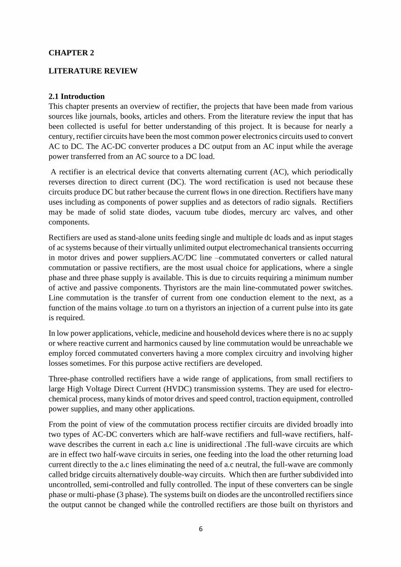
2.2.1.2 Single-Phase controlled Half-Wave Rectifiers
Unlike the diode, the silicon controlled rectifier (SCR) will not to begin to conduct as soon as
the source becomes positive . Gate trigger current is the minimum current required to switch
silicon controlled rectifiers from the off-state to the on-state at the specified off-state voltage
and temperature. Once the SCR is conducting, the gate current can be removed and the SCR
remains on until the current goes to zero . Figure 9 shows a basic controlled half-wave rectifier.
Figure 9: A basic half wave controlled rectifier
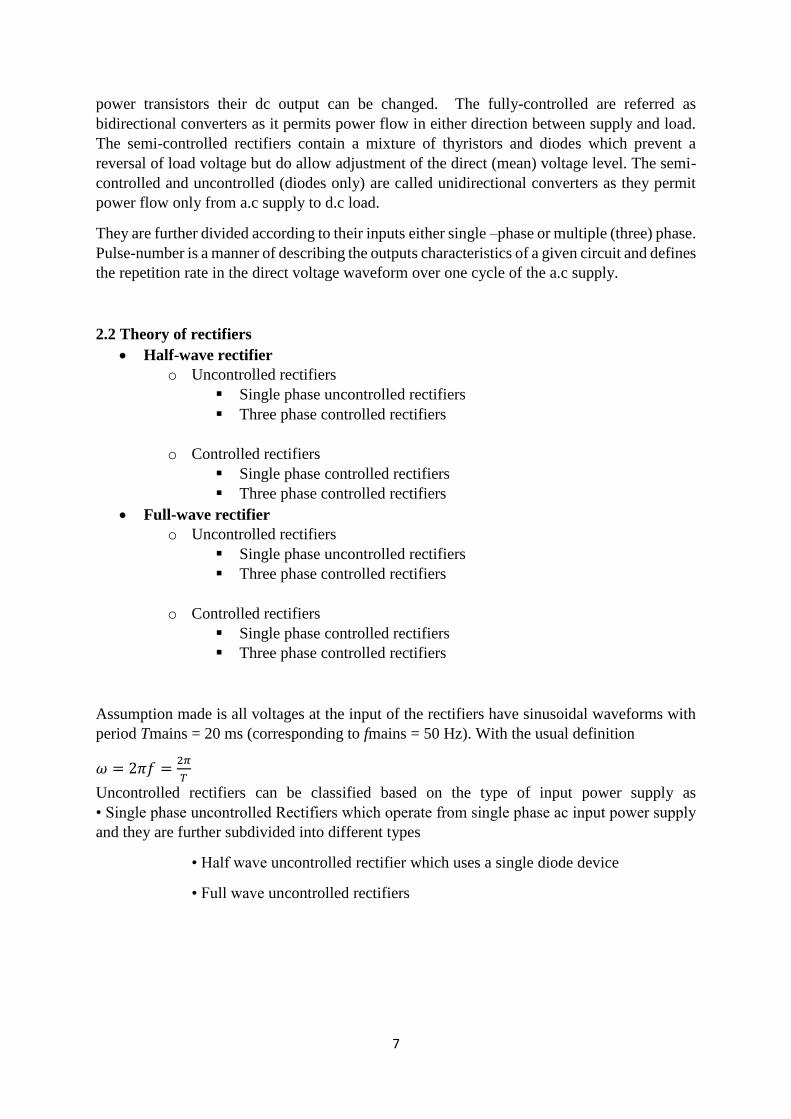
2.2.1.3: Single Phase Full-Wave Rectifiers
A single-phase full-wave rectifier consists of four diodes arranged as shown in figure 10 and
figure 11 are a bridge rectifier and the center-tapped rectifier. This rectifier circuit produces an
output waveform that is the positive half of the incoming AC voltage waveform and the
inverted negative half.
Figure10 a: The Bridge Rectifier Figure 10 b: single diode rectifier waveforms

12
Figure 10 c: The center-Tapped Transformer rectifier
The output voltage of single phase uncontrolled rectifier in eqn(2.3)
(2.3)
The lower peak diode voltage in the bridge rectifier which consists of four diodes arranged
makes it more suitable for high-voltage applications. Thus, the center-tapped transformer
rectifier in addition to including electrical isolation has only one diode voltage drop between
the source and load making it desirable for low-voltage and high current applications.
Figure 11: a full wave controlled bridge rectifier
Similar to the diode bridge rectifier topology, a versatile method of controlling the output of a
full-wave rectifier is to substitute controlled switches such as SCRs for the diode. Because of
their unique ability to be controlled, the output voltage and hence the power can be controlled
to desire levels. The triggering of the thyristor has to be synchronized with the input sinusoidal
voltage in an AC to DC rectifier circuit. The delay angle α is the angle interval between the
forward biasing of the SCR and the gate signal application Otherwise, if the delay angle is zero,
the rectifiers behave exactly like uncontrolled rectifiers with diodes. Figure 11 shows a basic
controlled full-wave rectifier.
(2.4)
13
2.2.2 Three Phase Rectifiers
Three phase rectifiers are commonly used in industry to produce a DC voltage and current for
large loads.In industrial applications, where three-phase AC voltages are available, three phase
rectifiers are favorable. At the output of this type of rectifier compared to the single-phase
rectifiers, the DC component is higher, the ripple of the output voltage is lower, and the output
power is higher. Like single phase rectifiers, three phase rectifiers also have two types that are
uncontrolled and controlled.
Three phase rectifiers are more commonly used because of the following reasons:
i. Three phase AC power is readily available.
ii. It is economical to provide DC supply to DC motors of capacity 20kW and more
from a three phase rectifier rather than single phase.
iii. The ripple frequency of the output current of the three phase rectifiers is higher than
that for single phase ones.
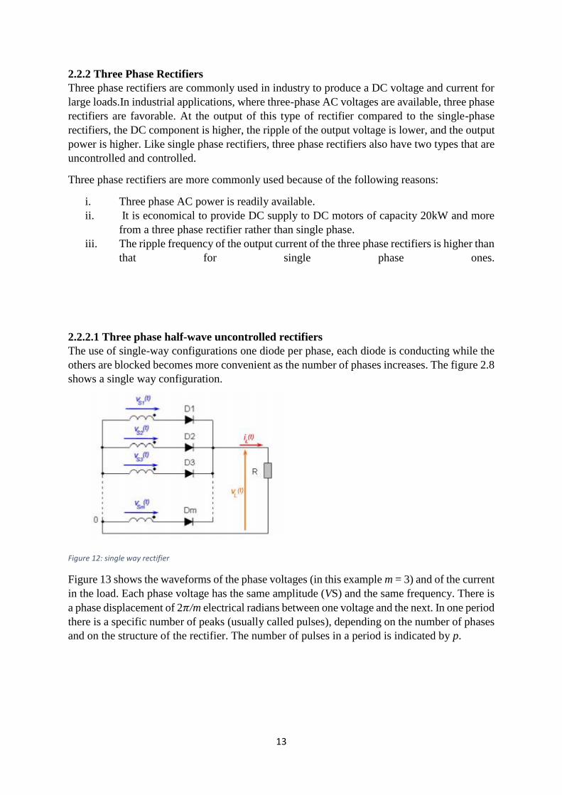
2.2.2.1 Three phase half-wave uncontrolled rectifiers
The use of single-way configurations one diode per phase, each diode is conducting while the
others are blocked becomes more convenient as the number of phases increases. The figure 2.8
shows a single way configuration.
Figure 12: single way rectifier
Figure 13 shows the waveforms of the phase voltages (in this example m = 3) and of the current
in the load. Each phase voltage has the same amplitude (VS) and the same frequency. There is
a phase displacement of 2𝜋/m electrical radians between one voltage and the next. In one period
there is a specific number of peaks (usually called pulses), depending on the number of phases
and on the structure of the rectifier. The number of pulses in a period is indicated by p.

14
Figure 13: waveforms for the number of pulses of single way rectifier
2.2.2.2 Three phase full wave uncontrolled rectifiers
Three phase full-bridge rectifier use diodes as switch. A simplified circuit by assuming an
idealized drive and by replacing a real load by a current generator. Due to neglecting the series
inductances of the driving generators, three phase rectifier divides into two groups which are
top group and bottom group. For top group, diode with its anode at the highest potential will
conduct at one time. The other two will be reversed. Thus for bottom group, diode with its
cathode at the lowest potential will conduct. The other two will be reversed. Figure 2.15 a
shows the phase voltage and the resulting combinations of line-to-line voltages from a balanced
three phase source. The output voltage is equal to the difference of the voltages at the points P
and N compared to the neutral point n,
𝑉𝑜 = 𝑉𝑝𝑛 − 𝑉𝑁𝑛 (2.5)
Since one diode of the upper group and one diode of the lower group are always conducting,
the voltages VPn and VNn are equal to one of the AC voltages Van,Vbn or Vcn . So, the output
voltage follows in turn six sinusoidal voltage during one cycle as shown in Figure 14 b these
been 𝑉𝑎 − 𝑉𝑏, 𝑉𝑎 − 𝑉𝑐, 𝑉𝑏 − 𝑉𝑐, 𝑉𝑏 − 𝑉𝑎, 𝑉𝑐 − 𝑉𝑎, 𝑉𝑐 − 𝑉𝑏 all having the maximum value
of the line voltage that is √3 times the phase voltage and for this reason, these rectifiers are
often called the six-pulse rectifiers. The output voltage during one cycle practically consists of
six sinusoidal peaks thus its ripple is small and the average value is close to the amplitude of
the line voltages. The phase currents are determined by
Figure 14: Three - phase bridge rectifier (a) and (b) it’s ideal equivalent circuit
15
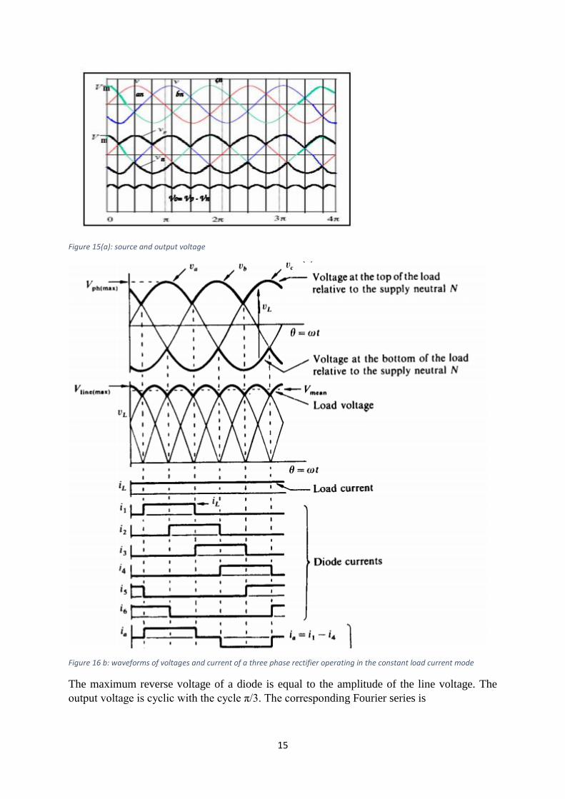
Figure 15(a): source and output voltage
Figure 16 b: waveforms of voltages and current of a three phase rectifier operating in the constant load current mode
The maximum reverse voltage of a diode is equal to the amplitude of the line voltage. The
output voltage is cyclic with the cycle π/3. The corresponding Fourier series is

16
(2.6)
Where the average value is
𝑉𝑎𝑣𝑟 = 2 ×3√3
2𝜋 Vph (max) (2.7)
Or calculated from the six-pulse load voltage waveform which is
𝑉𝑚𝑒𝑎𝑛 =3
𝜋𝑉𝑙𝑖𝑛𝑒(𝑚𝑎𝑥) (2.8)
Therefore, the average value of the output voltage is approximately equal to the amplitude of
the line voltage, 𝑉𝑙𝑖𝑛𝑒(𝑚𝑎𝑥)
The diode current waveforms shown in figure 2.11b reveal that each diode conducts the full-
load currents for one third of a cycle that is 𝜋
3𝑜𝑓 𝑡ℎ𝑒 𝑐𝑦𝑐𝑙𝑒, the order of commutation
determining the numbering of the diodes in circuit. Each diode conducts during 120°. They
conduct in pairs (6, 1), (1, 2), (2, 3), (3, 4), (4, 5), (5, 6), and (6, 1). Diodes turn on in the
sequence 1, 2, 3, 4, 5, 6, 1…
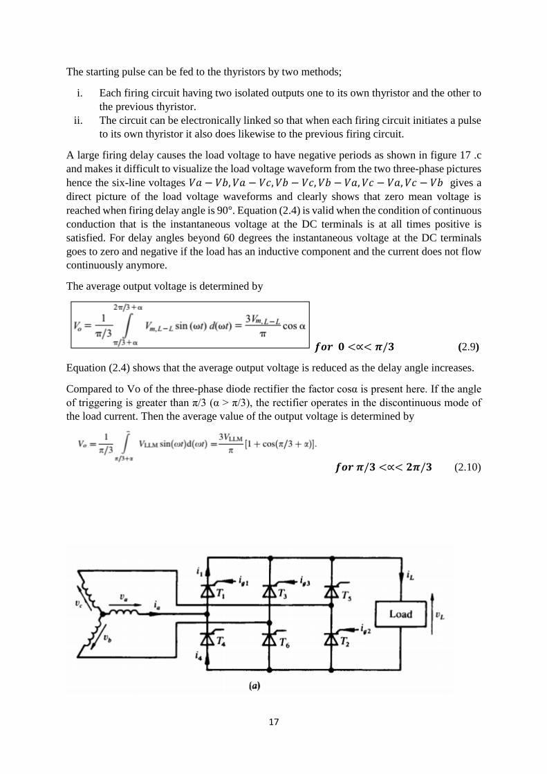
2.2.2.3 Three phase Controlled Rectifiers
Similar to single phase controlled rectifier, the output of the three phase rectifier can be
controlled by replacing the diodes with thyristors (SCRs). Figure. 17 a shows the controlled
six-pulse three phase rectifier. Thyristor is a device whose transition from the blocking to the
conducting state depends not only on the polarity of the anode–cathode voltage as for diodes,
which are naturally commutating devices but is also controlled via the application of an
adequate current pulse at the gate terminal. Thyristors have three terminals the trigger pulse is
applied to the gate while the anode–cathode voltage is positive. The difference in the principle
of operation is that the diodes are conducting when forward biased and the thyristors conducts
if a triggering pulse is present in the gate circuit together with the forward bias, this is the way
of controlling the angle of conduction and consequently the average value of the output voltage.
Thus, the transition of the output voltage to the maximum instantaneous line-to-line source
voltage can be delayed. The delay angle α is the interval between when the SCR becomes
forward-biased and when the gate signal is applied.
In this circuit there is a problem which is the one of starting .when connected to the three phase
a.c. supply firing gate pulses will be delivered to the thyristors and it must be in the correct
sequence but if only a single firing gate pulse is used no current will flow as the other thyristor
in the current path will be in the off-state. In order to start the circuit functioning two thyristors
must be fired at the same time in order to commence current flow. From the supply of three
phase when Va is at its peak value or its more positive the next firing pulse will be to
thyristor T2 however thyristor T2 will not conduct unless at the same time T1 is pulsed.
Reference to the waveforms shown in fig.17 b this shows that there are two thyristors
conducting at that instance. Hence for starting purposes the firing circuit must produce a firing
pulse 60° after its first pulse .Once the circuit is running normally the second pulse will have
no effect as the thyristor will already be in the on-state.
17
The starting pulse can be fed to the thyristors by two methods;
i. Each firing circuit having two isolated outputs one to its own thyristor and the other to
the previous thyristor.
ii. The circuit can be electronically linked so that when each firing circuit initiates a pulse
to its own thyristor it also does likewise to the previous firing circuit.
A large firing delay causes the load voltage to have negative periods as shown in figure 17 .c
and makes it difficult to visualize the load voltage waveform from the two three-phase pictures
hence the six-line voltages 𝑉𝑎 − 𝑉𝑏, 𝑉𝑎 − 𝑉𝑐, 𝑉𝑏 − 𝑉𝑐, 𝑉𝑏 − 𝑉𝑎, 𝑉𝑐 − 𝑉𝑎, 𝑉𝑐 − 𝑉𝑏 gives a
direct picture of the load voltage waveforms and clearly shows that zero mean voltage is
reached when firing delay angle is 90°. Equation (2.4) is valid when the condition of continuous
conduction that is the instantaneous voltage at the DC terminals is at all times positive is
satisfied. For delay angles beyond 60 degrees the instantaneous voltage at the DC terminals
goes to zero and negative if the load has an inductive component and the current does not flow
continuously anymore.
The average output voltage is determined by
𝒇𝒐𝒓 𝟎 <∝< 𝝅/𝟑 (2.9)
Equation (2.4) shows that the average output voltage is reduced as the delay angle increases.
Compared to Vo of the three-phase diode rectifier the factor cosα is present here. If the angle
of triggering is greater than π/3 (α > π/3), the rectifier operates in the discontinuous mode of
the load current. Then the average value of the output voltage is determined by
𝒇𝒐𝒓 𝝅/𝟑 <∝< 𝟐𝝅/𝟑 (2.10)
18
(b)
Figure 17: (a) fully-controlled three phase bridge ciruit, (b) the output voltage waveforms with small fring angle and (c) with large firing angle
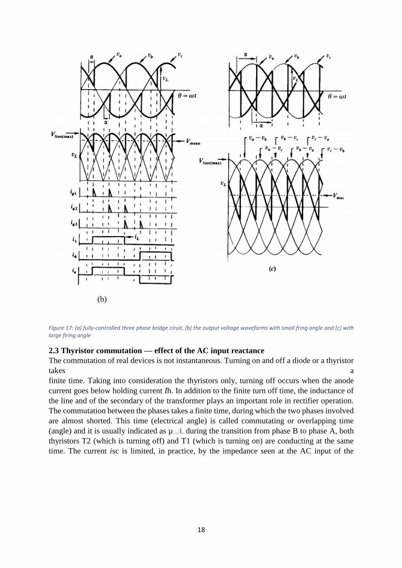
2.3 Thyristor commutation — effect of the AC input reactance
The commutation of real devices is not instantaneous. Turning on and off a diode or a thyristor
takes a
finite time. Taking into consideration the thyristors only, turning off occurs when the anode
current goes below holding current Ih. In addition to the finite turn off time, the inductance of
the line and of the secondary of the transformer plays an important role in rectifier operation.
The commutation between the phases takes a finite time, during which the two phases involved
are almost shorted. This time (electrical angle) is called commutating or overlapping time
(angle) and it is usually indicated as µ during the transition from phase B to phase A, both
thyristors T2 (which is turning off) and T1 (which is turning on) are conducting at the same
time. The current isc is limited, in practice, by the impedance seen at the AC input of the

19
rectifier, here indicated as LS.
Figure 18: Commutation of thyristor from one phase to another
Assuming the dc current ID to be smooth, and with the help of figure 18, the following relation
is deducted:
(2.20)
where isc is the current in the valve being fired during the commutation process (thyristor T2
in figure 18). This current can be evaluated, and it yields:
𝐼𝑠𝑐 =√2
2𝐿𝑠. 𝑉𝑓 − 𝑓
𝑐𝑜𝑠𝜔𝑡
𝜔+ 𝐶 (2.11)
The constant “C” is evaluated through initial conditions at the instant when T2 is ignited. In
terms of angle, when wt=α:
Where wt=α, 𝐼𝑠𝑐 = 0
Therefore
𝐶 =𝑉𝑓−𝑓
2𝐿𝑠. 𝑐𝑜𝑠 α (2.12)
During the commutation time, the load current ID remains constant, isc returns through T1,
and T1 is automatically switched-off when the current isc reaches the value of ID. This happens
because thyristors cannot conduct in reverse direction. At this moment, the overlap time lasts
µ, and the current ID is then conducted by T2. In terms of angle:
20
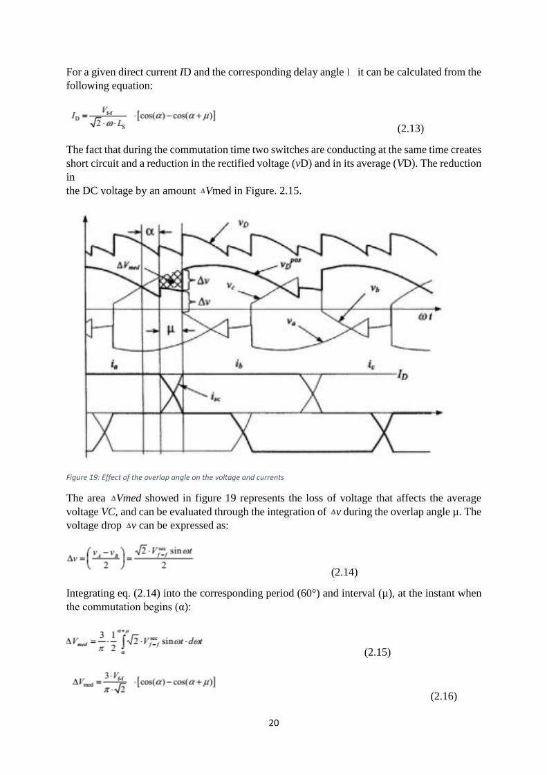
For a given direct current ID and the corresponding delay angle it can be calculated from the
following equation:
(2.13)
The fact that during the commutation time two switches are conducting at the same time creates
short circuit and a reduction in the rectified voltage (vD) and in its average (VD). The reduction
in
the DC voltage by an amount Vmed in Figure. 2.15.
Figure 19: Effect of the overlap angle on the voltage and currents
The area Vmed showed in figure 19 represents the loss of voltage that affects the average
voltage VC, and can be evaluated through the integration of v during the overlap angle µ. The
voltage drop v can be expressed as:
(2.14)
Integrating eq. (2.14) into the corresponding period (60°) and interval (µ), at the instant when
the commutation begins (α):
(2.15)
(2.16)

21
As can be seen in Figure 2.15, the waveform of the rectified voltage vD is additionally distorted
during the overlapping angle, worsening the output ripple of the rectifier.
(2.17)
(2.18)
The load current can be written as a function of the primary winding of the transformer, if any.
(2.19)
(2.20)
Where a=Vf-fsec/Vf-fprim.
2.4 Power displacement factor and Power factor
The angular displacement between the fundamental components of the.AC line current and the
associated line to neutral voltage.The Displacement Power Factor is defined as
DPF = cos1 (2.21)
cos = 𝑐𝑜𝑠𝛼
In the case of non-sinusoidal current, the active power delivered per phase by the sinusoidal
supply is
𝑃 =1
𝑇∫ 𝑣𝑎(𝑡)𝑖𝑎(𝑡)𝑑𝑡
𝑇
0 = 𝑉𝑎
𝑟𝑚𝑠𝐼𝑎𝑟𝑚𝑠cos1 (2.22)
Where Vrms is the rms value of the voltage va, and Ia 1rms the rms value of ia1 (fundamental
component of ia). Analog relations can be obtained for vb and vc.
The apparent power per phase is given by:
(2.23)
The power factor is defined by:
(2.24)

22
Where PF becomes:
(2.25)
This equation shows clearly that due to the non-sinusoidal waveform of the currents, the power
factor of the rectifier is negatively affected both by the firing angle α and by the distortion of
the input current. In effect, an increase in the distortion of the current produces an increase in
the value of Iarms in equation (2.24), which deteriorates the power factor.
Considering now the r.m.s. value of the distortion component in the line current,
(2.26)
The total harmonic distortion is given as
(2.27)
2.5 Effects on the AC mains voltage
During the commutation of the thyristors the two phases involved are almost shorted through
the line/transformer secondary reactance. This causes notches on the AC voltage. It can be
demonstrated that these notches have a maximum depth and width depending on the delay
angle α ,the line/transformer secondary reactance LS, the phase-to-phase voltage Vf-f, and the
average value of the rectified current ID.
(2.28)
The total harmonic distortion of the mains AC voltage can be calculated from the impedance
of the
AC source the line feeding the primary of the rectifier’s transformer LSline and the harmonics
of the converter’s input current. The THD can thus be given by
(2.29)

23
2.6 How to reduce the harmonics on the AC mains
Various techniques of improving the input current waveform are discussed below. The intent
of all techniques is to make the input current more continuous so as to reduce the overall current
harmonic distortion. The different techniques can be classified into four broad categories:
i. Introduction of line reactors and/or DC link chokes
ii. Passive filters (series, shunt, and low pass broadband filters)
iii. Phase multiplication (12-pulse, 18-pulse rectifier systems)
iv. Active harmonic compensation
The term three-phase line reactor or just reactor is used in the following paragraphs to denote
three-phase line inductors.
2.6.1 Three-Phase Line Reactors
Line reactors offer a significant magnitude of inductance that can alter the way the current is
drawn by a nonlinear load such as a rectifier bridge. The reactor makes the current waveform
less discontinuous, resulting in lower current harmonics. Since the reactor impedance increases
with frequency, it offers larger impedance to the flow of higher order harmonic currents.
Therefore, it is instrumental in impeding higher frequency current components while allowing
the fundamental frequency component to pass through with relative ease. On knowing the input
reactance value, one can estimate the expected current harmonic distortion. A table illustrating
the typically expected input current harmonics for various amounts of input reactance is shown
in Table 1.
Input reactance is determined by the accumulated impedance of the AC reactor, DC link choke
(if used), input transformer, and cable impedance. To maximize the input reactance while
minimizing AC
Table 1: percent Harmonics vs Total line impedances
Voltage drop, one can combine the use of both AC-input reactors and DC link chokes. One can
approximate the total effective reactance and view the expected harmonic current distortion
from Table 1. The effective impedance value in percent is based on the actual loading and is:
(2.30)
Where Iact (fnd.) is the fundamental value of the actual load current and VL−L is the line-line
voltage. The effective impedance of the transformer as seen from the nonlinear load is:

24
(2.31)
Where Zeff,x-mer is the effective impedance of the transformer as viewed from the nonlinear
load end; Zx-mer is the nameplate impedance of the transformer; and Ir is the nameplate rated
current of the transformer
2.6.2 DC-Link Choke
Based on the above discussion, it can be noted that any inductor of adequate value placed
between the AC
source and the DC bus capacitor of the ASD will help in improving the current waveform.
These observations lead to the introduction of a DC-link choke, which is electrically present
after the thyristor rectifier and before the DC bus capacitor. The DC-link choke performs very
similar to the three-phase line inductance. The ripple frequency that the DC-link choke has to
handle is six times the input AC frequency for a six-pulse ASD. However, the magnitude of
the ripple current is small. One can show that the effective impedance offered by a DC-link
choke is approximately half of that offered by a three-phase AC inductor. In other words, a 6%
DC-link choke is equivalent to a 3% AC inductor from an impedance viewpoint. This can be
mathematically derived equating AC side power flow to DC side power flow as follows:
𝑃𝑎𝑐 = 3 ×𝑉𝐿−𝑁
2
𝑅𝑎𝑐; 𝑃𝑎𝑐 = 𝑃𝑑𝑐 (2.32)
VL −N is the line-neutral voltage at the input to the three-phase rectifier.
𝑃𝑑𝑐 =𝑉𝐷𝐶
2
𝑅𝑑𝑐; (2.33)
𝑉𝑜 =3×√2×𝑉𝐿−𝐿×𝐶𝑂𝑆(𝛼)
𝜋=
3×√2×𝑉𝐿−𝑁×𝐶𝑂𝑆(𝛼)
𝜋 (2.34)
Hence 𝑅𝑑𝑐 = 2(9
𝜋2)𝑅𝑎𝑐 (2.35)
2.6.3 Passive Filters
Passive filters consist of passive components like inductors, capacitors, and resistors arranged
in a predetermined fashion either to attenuate the flow of harmonic components through them
or to shunt the harmonic component into them. Passive filters can be of many types. Some
popular ones are series passive filters, shunt passive filters, and low-pass broadband passive
filters. Series and shunt passive filters are effective only in the narrow proximity of the
frequency at which they are tuned. Low-pass broadband passive filters have a broader
bandwidth and attenuate almost all harmonics above their cutoff frequency.passive filter
components can interact with existing transformers and power factor correcting capacitors
and could create electrical instability by introducing resonance into the system. Some forms
of low-pass broadband passive filters do not contribute to resonance but they are bulky,
expensive, and occupy space. A typical low-pass broadband filter structure popularly
employed by users of ASDs .

25
2.6.4 DC side harmonic filtering
The fundamental ripple frequency is given by;
(2.36)
where p is the number of pulses.
The ripple voltage at the output of the rectifier can be represented as an independent time
varying voltage over/imposed on the average value of the rectified voltage (VDC). In order to
reduce the ripple amplitude, a passive LC filter is usually connected between the rectifier and
the load. The time-varying voltage can thus be interpreted as a composition of harmonics that
are individually weakened by the filter.
passive LC filters are used to reduce the harmonics content on the output
of the rectifiers: “a combination of L and C produces a lower ripple with normal components
values than is possible with either L or C alone” . The inductance smoothens the oscillations
in the current and the capacitance those in the voltage. The resonance frequency is given by
(2.37)
and it has to be chosen so as to satisfy the condition f0 << fr; furthermore, for a given f0, a
degree of freedom remains in the choice of L or C.
The critical inductance is calculated with the condition that the peak of the fundamental
harmonics of the current ripple through the filter inductance is equal to the minimum IDC in
the load.
(2.38)
where V ripple_1 is the amplitude of the fundamental harmonic of the ripple at frequency
fr_1. In order to avoid resonances, a damping resistor is normally added in the filter structure.
A typical scheme for a damped LC filter is given in Fig. .

26
Figure 20: passive filter
The resistance is chosen so as to limit the overshoot in the step response of the filter. From
the equation of the systems of the second order, with an overshoot equal to 1.5, the equations
for this type of filter are reported in (eqn 2.39 )
(2.39)
2.7 Silicon Controlled Rectifier
The thyristor is a solid-state semiconductor device with four layers of alternating N and P-type
material. They act as a switch, conducting when their gate receives a current pulse, and continue
to conduct for as long as they are forward biased (that is, as long as the voltage across the
device has not reversed).
Some sources define silicon controlled rectifiers and thyristors as synonymous; others define
SCRs as a subset of thyristors, along with gate turn-off thyristor (GTO), triode ac switch (triac),
static induction transistor (SIT), static induction thyristor (SITH) and MOS-controlled thyristor
(MCT). Among the latter, the International Electro technical Commission 60747-6 standard
27
stands out. Non-SCR thyristors include devices with more than four layers, such as triacs and
DBGTOs.
The thyristor is a four-layer semiconducting device, with each layer consisting of alternately
N-type or P-type material, for example P-N-P-N. The main terminals, labeled anode and
cathode, are across the full four layers, and the control terminal, called the gate, is attached to
p-type material near to the cathode. (A variant called an SCS Silicon Controlled Switch brings
all four layers out to terminals.) The operation of a thyristor can be understood in terms of a
pair of tightly coupled Bipolar Junction Transistors, arranged to cause the self-latching action:
Figure 21: two- transistor model of the thyristor (SCR) (a and b) and its symbol
2.7.1 Working of SCR
Thyristor act in three states:
Reverse blocking mode -- Voltage applied in the direction that would be blocked by a diode .
Forward blocking mode -- Voltage applied in the direction that would cause a diode to conduct,
but the thyristor has not yet been triggered into conduction.
Forward conducting mode -- The thyristor has been triggered into conduction and will remain
conducting until the forward current drops below a threshold value known as the "holding
current"
Figure 22: layer diagram of thyristor
When the anode is at a positive potential VAK with respect to the cathode with no voltage
applied at the gate, junctions J1 and J3 are forward biased, while junction J2 is reverse biased.
As J2 is reverse biased, no conduction takes place (Off state). Two ways of switching On SCR.
If VAK is increased beyond the breakdown voltage VBO of the thyristor, avalanche breakdown
of J2 takes place and the thyristor starts conducting (On state).

28
If a positive potential VG is applied at the gate terminal with respect to the cathode, the
breakdown of the junction J2 occurs at a lower value of VAK. By selecting an appropriate
value of VG, the thyristor can be switched into the on state immediately. It should be noted
that once avalanche breakdown has occurred, the thyristor continues to conduct, irrespective
of the gate voltage, until either: (a) the potential VG is removed or (b) the current through the
device (anode−cathode) is less than the holding current specified by the manufacturer. Hence
VG can be a voltage pulse, such as the voltage output from a UJT relaxation oscillator.[6]
These gate pulses are characterized in terms of gate trigger voltage (VGT) and gate trigger
current (IGT). Gate trigger current varies inversely with gate pulse width in such a way that it
is evident that there is a minimum gate charge required to trigger the thyristor.[2,6]
2.7.2 Switching Characteristics of SCR
In a conventional thyristor, once it has been switched on by the gate terminal, the device
remains latched in the on-state (i.e. does not need a continuous supply of gate current to
conduct), providing the anode current has exceeded the latching current (IL). The thyristor will
remain in the on state (the region of low resistance) as long as the anode current is higher than
the holding current, IH . The holding current is the lowest anode current maintaining the
thyristor in the state of conduction with the gate open (IG = 0) [6, 5].
Figure 23: The static V-I characteristic of an SCR
A thyristor can be switched off if the external circuit causes the anode to become negatively
biased. In some applications this is done by switching a second thyristor to discharge a

29
capacitor into the cathode of the first thyristor. This method is called forced commutation. After
a thyristor has been switched off by forced commutation, a finite time delay must have elapsed
before the anode can be positively biased in the off-state. This minimum delay is called the
circuit commutated turn off time (tQ). Attempting to positively bias the anode within this time
causes the thyristor to be self-triggered by the remaining charge carriers (holes and electrons)
that have not yet recombined [6].
For applications with frequencies higher than the domestic AC mains supply (e.g. 50 Hz or 60
Hz), thyristors with lower values of tQ are required. Such fast thyristors are made by diffusing
into the silicon heavy metals ions such as gold or platinum which act as charge combination
centers. Alternatively, fast thyristors may be made by neutron irradiation of the silicon [6, 7].
2.7.3 SCR Ratings
A data sheet for a typical thyristor follows this section and includes the following
information:
Surge Current Rating (IFM)—The surge current rating (IFM) of an SCR is the peak anode
current a SCR can handle for a short duration.
Latching Current (IL) — a minimum anode current must flow through the SCR in order for it
to stay ON initially after the gate signal is removed. This current is called the latching current
(IL).
Holding Current (IH) — After the SCR is latched on, a certain minimum value of anode
current is needed to maintain conduction. If the anode current is reduced below this minimum
value, the SCR will turn OFF.
Peak Repetitive Reverse Voltage (VRRM)—the maximum instantaneous voltage that an SCR
can withstand, without breakdown, in the reverse direction.
Peak Repetitive Forward Blocking Voltage (VDRM)—the maximum instantaneous voltage
that the SCR can block in the forward direction. If the VDRM rating is exceeded, the SCR
will conduct without a gate voltage.
Non-repetitive Peak Reverse Voltage (VRSM) — the maximum transient reverse voltage that
the SCR can withstand.
Maximum Gate Trigger Current (IGTM) — the maximum DC gate current allowed to turn
the SCR ON.
Minimum Gate Trigger Voltage (VGT) — The minimum DC gate-to-cathode voltage
required to trigger the SCR.
Minimum Gate Trigger Current (IGT) — The minimum DC gate current necessary to turn the
SCR ON .
2.7.4 Gate Circuit Requirements.
The trigger signal should have voltage amplitude greater than the minimum gate trigger
voltage of the thyristor being turned ON. It should not be greater than the maximum gate
trigger voltage, either. The gate current should likewise be in between the minimum and
maximum values specified by the thyristor manufacturer. Low gate current driver circuits can
fail to turn ON the thyristor [7].
The thyristor is a current controlled switch and so the gate circuit should be able to provide
the needed turn ON gate current into the thyristor. Sufficient gate trigger current will turn ON
the thyristor and current will flow from the anode to the cathode provided that the thyristor is
favorably biased and the load is such that the current flowing is higher than the latching current

30
of the thyristor. The gate trigger will turn ON the thyristor only if it occurs during the positive
part of the AC .Any trigger signal during the negative part of the AC cycle will not turn ON
the thyristor and the thyristor will remain in blocking state. Keeping the gate signal ON during
the negative part of the AC cycle does not typically damage a thyristor [7].
The current into and the voltage at, the gate are both subject to maximum values, but turn-on
requirements demands they also exceed certain minimum levels. The product of gate and
current gives a power level to which a maximum is set.in figure 2.19 shows the limits imposed
on the gate cathode characteristic, giving the area into which must be fitted the gate firing signal
for certain firing into the on-state to take place. Final stage of gate triggering network consist
of a pulse transformer for isolation ,a resistor (R1) to limit the gate current and R2 to limit the
gate voltage when the thyristor is in the off state.[1]
(a)
(b)
Figure 24: (a) Firing network desirable network connection,(b) firing network load line
31
2.7.5 SCR protection
2.7.5.1 Overcurrent
The current rating of a device is the current which raises the temperature of the junction to its
top limit (normally around 125°C). An overcurrent will raise the temperature of the junction
excessively and cause malfunctions or the destruction of the device.
The simplest way to protect a thyristor is using adequate fuses. They must be fast acting fuses
preventing the rise to high arc voltages (less than 1.5 times the peak voltage in circuit). The
I2t parameter normally characterizes fuses: this value must be lower than the I2t that would
damage the thyristor (the semiconductor manufacturer usually indicates the maximum I2t for
the protection fuses).
2.7.5.2 Overvoltage
Withstanding the estimated reverse voltage for the application where it is used is one of the
main parameters for the design of the converter. If the thyristor is submitted to a reverse
voltage greater than its rated value, it will break down. Choosing oversized devices (VRRM
30% or 50% higher than that one expected) is a solution in this case.
2.7.5.3 Transients/ surges
Voltage transients or voltage surges, i.e., an excessive slew rate of voltage (dv/dt) are another
source of overvoltage that may damage the thyristors. Transients may originate from sources
that are either internal or external to the device.
The general approach to protect thyristors from voltage surges is to quickly store the surge
energy in a capacitor, and then to dissipate it slowly in a resistor. Each thyristor commutation
causes some transient voltage peaks, in particular at turn off. Owing to the presence of an
inductance (line, transformer winding, etc.) in series during its conduction phase, a high peak
reverse voltage is generated when the thyristor is turned off. In order to mitigate this voltage
surge, a RC combination, called snubber circuit, is connected in parallel to each device.
Capacitor C1 suppresses the voltage surge dv/dt that appears when the thyristor Th goes into
the blocking state. Resistor R (R1) is used to damp possible oscillations in the LC circuit (L is
the inductance of the AC connection seen by the thyristor). The same resistance R (or, in the
circuit on the right, R2) has to limit the discharge current from the capacitor through the
thyristor when it starts to conduct again.
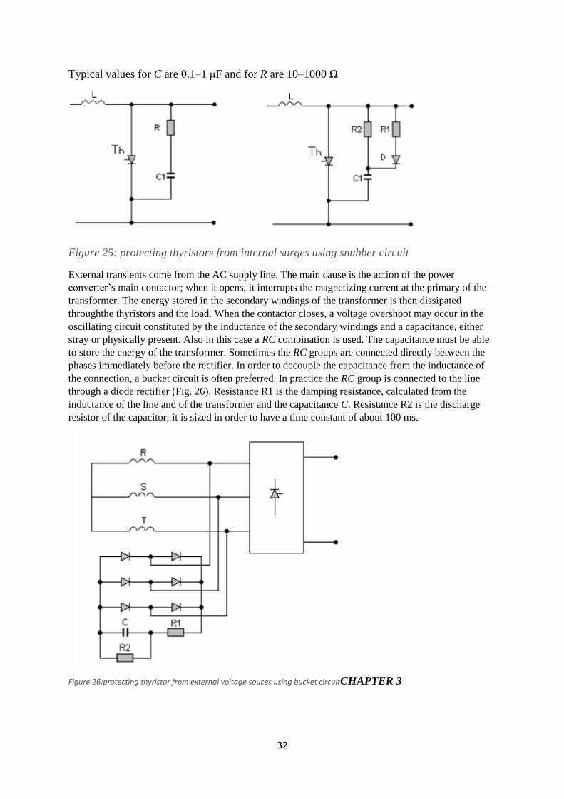
32
Typical values for C are 0.1–1 μF and for R are 10–1000 Ω
Figure 25: protecting thyristors from internal surges using snubber circuit
External transients come from the AC supply line. The main cause is the action of the power
converter’s main contactor; when it opens, it interrupts the magnetizing current at the primary of the
transformer. The energy stored in the secondary windings of the transformer is then dissipated
throughthe thyristors and the load. When the contactor closes, a voltage overshoot may occur in the
oscillating circuit constituted by the inductance of the secondary windings and a capacitance, either
stray or physically present. Also in this case a RC combination is used. The capacitance must be able
to store the energy of the transformer. Sometimes the RC groups are connected directly between the
phases immediately before the rectifier. In order to decouple the capacitance from the inductance of
the connection, a bucket circuit is often preferred. In practice the RC group is connected to the line
through a diode rectifier (Fig. 26). Resistance R1 is the damping resistance, calculated from the
inductance of the line and of the transformer and the capacitance C. Resistance R2 is the discharge
resistor of the capacitor; it is sized in order to have a time constant of about 100 ms.
Figure 26:protecting thyristor from external voltage souces using bucket circuitCHAPTER 3

33
METHODOLOGY
3.1 introduction
This project deals with the design, development and control of a 3-phase controlled rectifier
whose power circuit is shown in Fig. 3.1 it is the most widely rectifier circuit. It consists of a
three phase transformer in star / delta connection, six thyristor bridge connected, load , CLC
filter , synchronization circuits , the trigger control and isolation circuit.
This three phase rectifier circuit must be double-pulse triggered or trigger pulse width to ensure
that at every moment it has two thyristors in same turn or triggered at same time. The three
phase transformer is connected in star / delta connection so as to reduce a multiple a multiple
of 3 harmonic currents impacting on the power and have three phase inputs which have a phase
difference of 120°.
It is a common cathode connection and is made of the three-phase half-wave phase controlled
rectifier circuits and a common anode connection of the three phase half-wave phase controlled
in series circuit.
Figure 27: Three phase controlled rectifier circuits
The trigger circuit used in this paper is that of digital triggering and the trigger circuit is
controlled by a microcontroller unit belonging to the Atmel which is an Atmega328p
microcontroller. Its main feature includes generation of 6 channel trigger pulses whose time
interval is 60 degree; only needing a synchronization signal; shift phase range of 0 degrees to
160 degree; inputting shift phase angle by variation of a potentiometer which is displayed on a
LCD display.
Each thyristor requires a trigger pulse, so this trigger circuit needs to generate 6 trigger
pulses in all and a time interval of between the trigger pulses is 60 degrees.
A block diagram of the trigger circuit is shown in Figure 1. There is a microcontroller unit
(MCU) – ATMEGA 328P from ATMEL corporation- which controls the trigger circuit to
normally run and there are also other peripheral module circuits of the MCU including LCD
display, Zero crossing detector signals and trigger pulses output.
34
Figure 28: Tri-phase control rectifier block diagram
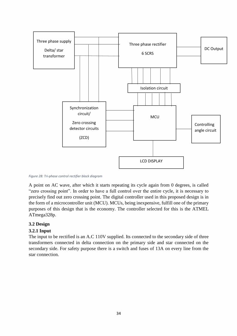
A point on AC wave, after which it starts repeating its cycle again from 0 degrees, is called
“zero crossing point”. In order to have a full control over the entire cycle, it is necessary to
precisely find out zero crossing point. The digital controller used in this proposed design is in
the form of a microcontroller unit (MCU). MCUs, being inexpensive, fulfill one of the primary
purposes of this design that is the economy. The controller selected for this is the ATMEL
ATmega328p.
3.2 Design
3.2.1 Input
The input to be rectified is an A.C 110V supplied. Its connected to the secondary side of three
transformers connected in delta connection on the primary side and star connected on the
secondary side. For safety purpose there is a switch and fuses of 13A on every line from the
star connection.
Three phase rectifier
6 SCRS
Three phase supply
Delta/ star
transformer
Synchronization
circuit/
Zero crossing
detector circuits
(ZCD)
MCU
Controlling
angle circuit
Isolation circuit
LCD DISPLAY
DC Output

35
Figure 29: The input circuit to rectifier
The transformers specifications were;
Primary inductance = 1H
Secondary inductance = 0.1H
Coupling factor=1.0
The virtual source connected to the primary side specifications;
Amplitude volts = 78v Vrms and frequency of 50Hz.
Fuse =13A rating
Vrms =Vm
√2 (3.1)
The Vm = 78v × √2 = 110.30v (3.2)
3.2.2 The rectifier circuit
The circuit below shows the connection of both rectifier connection, the snubber circuit,
isolation circuit and the filter of the dc at the output which is connected to a resistive load.

36
Figure 30: three phase connected to the supply with the snubber circuits and isolation circuit
Scr S4015L ratings
Vrmm/Vdrr = 200v (min)
Ig = 1 mA (min) and 20 mA (max) –the gate current
Vgt = 1.5 V max the dc gate trigger voltage
Ih = 30 mA the dc holding current;gate open
The SCR in this paper are gate triggered. Using the manufacturer ratings the calculations of the
gate voltage and currents and the components specified.
3.2.2.1 Snubber circuit.
The circuit is used for high dVD
dt protection of SCR the critical rate of rise of off- voltage.
Leakage current though the scr increases with the increase in 𝑑𝑣
𝑑𝑡 that is the rate of change of
applied voltage across the thyristor. This current can turn on the device even when the gate
signal is absent which is called the 𝑑𝑣
𝑑𝑡 and is avoided by using a Snubber circuit which
consists of a capacitor in series with a resistor applied parallel with the SCR.
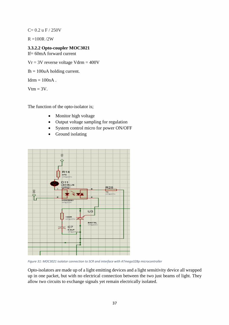
37
C= 0.2 u F / 250V
R =100R /2W
3.3.2.2 Opto-coupler MOC3021
If= 60mA forward current
Vr = 3V reverse voltage Vdrm = 400V
Ih = 100uA holding current.
Idrm = 100nA .
Vtm = 3V.
The function of the opto-isolator is;
Monitor high voltage
Output voltage sampling for regulation
System control micro for power ON/OFF
Ground isolating
Figure 31: MOC3021 isolator connection to SCR and interface with ATmega328p microcontroller
Opto-isolators are made up of a light emitting devices and a light sensitivity device all wrapped
up in one packet, but with no electrical connection between the two just beams of light. They
allow two circuits to exchange signals yet remain electrically isolated.

38
As seen in the figure 3.2 terminal IO3 is to a pin of the microcontroller interfaced with
MOC3021 ic pin 1 led in series, which glows to indicate a logic high pulse from the MCU
through a current limiting resistor so to that a current is flowing in internal led of the opto-ic.
Current flows from pin 1 to 2 and LED light falls on the DIAC causing pin 6 and 4 to close.
During each half cycles of the AC source current flows through gate , series resistor and
through opto-diac to the main SCR to trigger for the load to operate .
Ohms law;
𝑉 = 𝐼𝑅 (3.3)
𝑅 =𝑉
𝐼 (3.4)
The series resistor for current limiting is;
The LED must have 15mA and 1.2 V to light on the output voltage of the mcu is 5V.
𝑅 =5𝑉−1.2𝑉
0.015 = 250R (3.5)
R= 250R
3.2.3 Synchronization circuit/ Zero crossing detector circuits.
To have full control over the firing angle of the SCRs (from 0 to π radians), it is necessary to
precisely detect the zero crossing of the sinusoidal input. Schematic of the zero crossing circuit
that was implemented is shown in fig 3.4
Figure 32: zero crossing circuit with input transformer
Since the rectifier has three phase supply three of this circuits are used so as to detect the zero
points of the three ac supply helping to trigger the SCRs in the correct sequence.
Transformer used is at the input side is used for two purposes. Firstly it scales down the mains
alternating voltage to a lower and safer value up to the 6 to 9 volts rms. This gives peak voltage
of 8.46 = √2*6 volts up to 12.728 = √2*9 volts, respectively. Secondly it provides the galvanic
isolation between mains and zero crossing detection circuitry that is another key goal of the
proposed design.

39
This scaled down and isolated AC input is then scaled down further by using a resistor
consisting on R8 and R9 and they are of equal values.
Vout = (R8/R9) × Vsec (3.6)
R11 and R12 = 10k
The transformer steps down the voltage = 10.5V
The 50Hz sine wave synchronization shift voltage from a power grid is transformed to
square-wave signal with same frequency as the sine and then the square-wave signal is sent to
the interrupt pin of the MCU which can received external interrupt.
controller circuit is required to sense the zero crossing instant of the input voltage and from
thereof generates six equidistant trigger pulses in each cycle (one time period or 20 ms) for
switching of SCR of three phase converter.
The maximum voltage that the zero crossing is 4.88 v which is applicable for the mcu .
Figure 33: square wave zero crossing signals of the two phases
3.3.3 Controlling voltage
Analog Voltage (0-5 V) is used for controlling the converter power, ADC of Atmega-328
microcontroller is 10 bit resolution. Analog Voltage (0-5 V) is converted in to (0-1023) count.
Analog voltage is provided to one of the channel of ADC port. As per variation in the analog
voltage there is change of digital value. ADC conversion takes around 250 micro second. PWM
is achieved with the help of variable controlling voltage.

40
Figure 34: Controlling Voltage circuit
3.3.4 Generating of the firing pulses
A supply of 5v dc is used in this the specification of this paper was to trigger the SCRs the
controlling analog circuit varies the input from 0v to 5v.
ADC of ATmega328p is of 10-bit resolution hence the maximum value from the ADC WITH
+5 volts reference will be of 0-5 V are 0-1023 counts therefore a scaling down factor of 5.68
is used.
The 0-5v range controls the firing angle 0° to 180°
The presented results were drawn by operating the system in 50 Hz mode due to the national
standard of power transmission in Kenya.
𝑓 =1
𝑇 (3.7)
So the period of the supply is;
𝑇 =1
𝑓 (3.8)
𝑇 =1
50= 0.02 = 20𝑚𝑠𝑒𝑐 (3.9)
Half cycle time the period is 10ms the delay angle can thus be calculated as ;
𝛼 = 𝐴𝐷𝐶/5.68 (3.10)
Where ;
ADC = the output of the ADC converter/ the counts
𝛼 =is the firing angle

41
The ADC reading is converted into a delay after which firing pulse is to be generated. using
equation(3.11)
𝑑 = (𝑎𝑑𝑐 ∗ 5) ∗ 1.955 (3.11)
d - delay in microseconds
adc is the output of the ADC
1.955- value is a scaling up factor for the ADC reading
5 -is the reference value
In the circuit a 4.7V zener diode is used so as to clump the voltage not to exceed 4.3 V due to
the specifications of this paper was for the firing angle not to exceed 163° firing angle
Table 2: the delay angle calculated table
Voltage value (V) ADC counts Angle (𝜶) Delay (d) ms
0 0 0 0
1 204.6 36.02 1.9999
1.5 306.9 53.87 2.9999
3 613.8 108.06 5.9999
4.3 879.78 154.48 8.5998
4.5 920.7 162.09 8.9998
The output of ATmega328p is 4.8V and a current of 10miliampers each pin. The current is
enough to trigger the SCR used which is has a maximum of gate current 20mA.
The triggering of the 6 scrs are in sequencial form.each of the 6 SCRs are switched at an interval
of 60° sequentially,from T1,T2,T3,T4,T5,T6,and the sequence repeats again after a complete
cycle. 60° translate to a delay of 3331.32 microseconds .
From the theory part for the flow of the current two SCRs must be conducting at the same time
forming a pair of SCRs conducting.as shown in the table
Table 3: The algorith of triggering the SCR
SCR pair conducting Angle in degrees Extracted line
voltage
T6 , T1 ∝+30 to ∝+90 Vab
T1 , T2 ∝+90 to ∝+150 Vac
T2,T3 ∝+150 to ∝+210 Vbc
T3,T4 ∝+210 to ∝+270 Vba
T4,T5 ∝+270to ∝+330 Vca
T5 ,T6 ∝+330 to ∝+30 Vcb
T6,T1 ∝+30 to ∝+90 Vab
The firing angle = ∝, a phase shift of 60°
Using table 3.2 helped In the programming of the microcontroller.

42
ATmega328p has been programmed for triggering the power circuit. The execution of the
program in step by step process is explained using a flowchart. Which is show the flowchart
below.
From the output of the zero crossing circuit which is a square wave on which shows where the
AC wave crosses the zero is an input to the ATmega328p and INT01 and INT1 from the three
synchronization circuits using the Pin-change interrupts of the microcontroller causes an
interrupt showing that a phase has crossed the zero point from figure 3.5 show that at the rising
edge of the square wave that is when the phase is on the positive half.
The MCU executes its interrupt service routine (ISR).the function of the ISR is to determine
how to generate rising edge of the first trigger pulse which for elimination of the starting
problem of the rectifier and it initializes Timer 1 in the MCU to start counting from 0 and
counts up until it hits the ‘TOP’ value which the ‘TOP’ value is from the varied voltage which
gives the desired delay divided by a factor and it fires an interrupt which then T1 is fired at 30°
approximately 1.667sec the first pulse is generated.by setting PORT D , bit-3 high and a delay
of 1 millisecond and then timer runs the second time when the timer overflows the MCU
executes ISR of the timer.In this routine PORTD,bit-5 is cleared this pin is connected to T1
since the time interval between the first pulse and the second pulse is 60° which is
approximately 3.334 millisecond which means the time interval between the falling edge of the
first pulse and the rising edge of the second pulse is t1=3.334-1=2.334ms,the timer runs the
third time and when it hits the ‘TOP’ value it overflows and the MCU executes the timer ISR
in the routine PORT D,bit-5 high connected to T2 and a second pulse to T1 both pins are set to
high to start the second trigger pulse and the following steps reapeat the generation process of
the first pulse until the other pulses are outputted at this point the zero-crossing wave of phase
two has caused an interrupt. The length of time of the timer is determined by shift angle ∝
inputted though varying the potentiometer.
Here timer 1 is as a 16-bit timer and operates in mode 1. The MCU has an external 16 MHz
oscillator and fuses are set to use the external crystal clock. Fuses are used to control things
like which oscillator to use and what speed to run , blowout detection and the size of the boot
flash.
The trigger pulses are outputted in a way that each thyristor is triggered twice that is a main
pulse and secondary pulse at 60° shift from the main pulse. pin PD3 outputs a main pulse to
thyristor 1 and at the same time PB3 outputs a secondary pulse to thyristor 6;pin PD5 outputs
main pulse to thyristor 2 at the same time pin PD3 outputs the secondary pulse to thyristor 1;pin
PD6 outputs the main pulse to thyristor 3 and at the same time pin PD5 outputs the secondary
pulse to thyristor 2;pin PB1 outputs a main pulse to thyristor 4 and at the same time pin PD6 a
secondary pulse to thyristor3;pin PB2 outputs a main pulse to thyristor 5 and at same time pin
PB1 a secondary pulse to thyristor 4;pin PB3 outputs a main pulse to thyristor 6 and at the same
time pin PB2 outputs a secondary pulse to thyristor 5. And this process repeats its self in the
cycles.

43
Figure 35: MCU and LCD display
Figure 36: waveform of the output pulse
3.4 Software Design
the software design includes the main program,the display subroutine and the analog voltage
varied that is the ADC conversion,the external interrupt service routine and the timer interrupt
service routine.
3.4.1 Main Program
In this program it initializes the pins which input and the output pins; that is the analog pin(PC0)
from the controlling voltage circuit and the ADC handling initialization, three interrupt pins
(PCINT8,PCINT10,PCINT11) from the three zero crossing detector , the output of the trigger
pulses pins with their corresponding thyristor (PD3-T1, PD5-T2, PD6-T3, PB1-T4, PB2-T5,
PB3-T6) and the display subroutine.

44
NO
NO YES
NO
YES
Figure3.9 flow chart for six-pulse generation
Start
Initialization of pins and ADC
conversion
Read the analog voltage and do a conversion (store the
counts)
Is the external
interrupt detected?
Clear the PCINT11 and provide a delay of 30°
Enable interrupt bits and wait for external pulse
Check if bit 3 is high?
Is the bit
3 high? Provide a pulse width of 1ms
Clear port D, bit3 Check the pcint10?
Is the interrupt
detected?
Interrupt ISR executed and start the timer
Timer overflow and provide a 60° delay
Check if pin required bit is high?
Provide a delay for pulse
Is the pin required
bit high?

45
3.4.2 ADC program for delay
NO
YES
Figure 37: flow chart ADC subroutine and delay control
ADC program for delay control
Set the PC0 as input
Enable interrupt bits, make AD mode ON
Start the conversion
Check for completion of conversion
Call delay routine
Set the pin required bit high
Provide a delay
Clear the pin set high
Return
Has the conversion
ended?

46
CHAPTER 4:
RESULTS AND ANALYSIS
4.1 Theoretical Results
This are on ideal case basis from the equation (4.1);
𝑉𝑑𝑐 =3√2
𝜋𝑉𝑙 × cos 𝛼 for 0 <∝<60° (4.1)
𝑉𝑜 =1
𝜋3⁄
∫ 𝑉𝑙𝑙𝑚 sin(𝜔𝑡) 𝑑(𝜔𝑡)𝜋
𝜋3+∝⁄
= 3𝑉𝑙𝑙𝑚
𝜋{1 + cos(𝜋
3⁄ + 𝛼)}
𝑓𝑜𝑟 60° <∝< 120°
𝑉𝑙 = 𝑅𝑀𝑆 𝑉𝑎𝑙𝑢𝑒 𝑜𝑓 𝑡ℎ𝑒 𝑙𝑖𝑛𝑒 − 𝑙𝑖𝑛𝑒 𝑣𝑜𝑙𝑡𝑎𝑔𝑒 =110𝑣
√2= 77.78𝑣
Table 4: ideal results
Firing angle Dc Voltage
0° 181.93V
30° 157.56V
70° 62.23V
130° 64.99V
Table 5 Simulated results
Firing angle Dc voltage

47
CHAPTER 5
CONCLUSION AND RECOMMENDATION
5.1 Conclusion
The project the software to trigger six thyristor or SCRs used in the power circuit of three-
phase, six pulse, and controlled rectifier has been discussed. Three fully controlled rectifiers
are very popular in many industrial applications particular in situations where power
regeneration from dc side is essential.in this the rectifier implemented was for use in the lab.
The design is isolated from electronic interference at input and output side. Power control is
possible by varying ∝ 𝑡ℎ𝑒 𝑓𝑖𝑟𝑖𝑛𝑔 𝑎𝑛𝑔𝑙𝑒 with controlling voltage with the use of ATmega328p
microcontroller and by programming the analog voltage given it controls the firing angle and
controls the dc voltage output.
The configuration used lends itself to easy series and parallel connection for increasing voltage
and current rating or improvement in harmonic behavior. Since three phase fully controlled
rectifier are obtained at the cost of increased circuit complexity due to the use of six SCRs and
their associated control circuit. This complexity can be reduced by using this software for easily
triggering the six SCRs. Moreover the trigger pulses generated by this software are
controllable.
5.2 Recommendations for Further Work
Following are areas of future study which can be considered for further research work.
1. Speed Control Of Motors
2. Transmission of HVDC

48
REFFERENCES
[1] R. Simard and V. Rajagopalan, “Economical equidistant pulse Firing scheme for
Thyristorized D.C. drives,” IEEE Trans. Ind. Electron. Contr. Instrum., vol. IECI-22, No.3, pp.
425-429, 1975
[2] Gangul M.R, G.P Jain, “Design and Implementation of AT Mega 328 microcontroller based
firing control for a tri-phase thyristor control rectifier,” International Journal of Engineering
Research & Technology (IJERT), 2013.
[3] R. Visintini, “Rectifiers,” Elettra Synchrotron Light Laboratory, Trieste, Italy
[4] Juan Dixon (Ph.D.). “Three phase controlled rectifiers,” Pontifical Universidad Católica de
Chile. Vicuña Mackenna 4860
[5] Branko Dokic, Branko Blanusa, “Power Electronics Converters and Regulators.”
[6] Mohd Helmi. “Control Rectifier for Variable Speed Single Phase DC Motor,” University
Malaysia Pahang.
[7] J. David Irwin, “The power electronics hand book,” Auburn University
[8] XU Wuxiong, “Design of Thyristor Digital Trigger Circuit Based on Microcontroller Unit,”
The 1st International Conference on Information Science and Engineering (ICISE2009)
[9] Daniel W. Hart, “power electronics,” mc craw-hill
[10] Suhel Mustajab, Mohd. Kashif Adhami, “Software based approach for Triggering 3-phase,
6-pulse, AC to DC Controlled Converter,” International Journal of Advanced Research in
Computer Engineering & Technology (IJARCET) ,Volume 1, Issue 9, 2014.
[11] Shashikant V. Lahade1 and S. R. Hirekhan2, “Microcontroller based Digital Trigger
Circuit for Converter, Proc. of Int. Conf. on Advances in Power Electronics and
Instrumentation Engineering, PEIEs
[12] R. Arockiasamy and S. Doraipandy, “A novel trigger scheme for Thyristor operating under
variable frequency anode supply,” IEEE Trans. Ind. Electron. Contr .Instrum., vol. IECI-22,
No. 1, pp. 83-85, Feb.1975.
[13] Cyril W. Lander, “power electronics,”
[14] S. Murugesan and C.Kameswara, "Simple adaptive analog and Digital trigger circuits for
thyristors working under wide range of Supply frequency,” IEEE Trans. Ind. Electron. Contr.
Instrum., vol. IECI-24, No. 1, pp.46-49, 1977.
[15] L.H.Hoang ,"A digitally controlled thyristor trigger circuit," Proc. IEEE, vol. 66, No.1,
pp. 89-91, Jan. 1978.
[16] B. Ilango, R. Krishman, R. Subramanian, and S. Sadasivam, “Firing circuit for three-phase
thyristor rectifier IEEE Trans. Ind. Electron. Contr. Instrum., vol. IECI-25, no. 1, pp. 45-49,
1978.
[17] S.C.Gupta, K.Venkatesan, and K.Eape Generalized Firing Angle Controller Using Phase
Loop for Thyrist Control,” IEEE Transactions On Industrial Electronics And Control
Instrumentation, vol. IECI-28, No. 1, February 1981
[18] John William,“introduction to solid state power electronics,” POWEREX, Inc.
200 Hillis Street Youngwood, PA 15697-1800
[19] A.W. Kelley and W.F. Yadusky, Rectifier design for minimum line-current harmonics and
maximum power factor, IEEE Trans. Power Electron. 7 (1992) 332.