power failure monitoring unit - university of...
TRANSCRIPT

UNIVERSITY OF NAIROBI
DEPARTMENT OF ELECTRICAL AND ELECTRONICS ENGINEERING
PROJECT 106: POWER SYSTEM FAILURE MONITORING UNIT
NAME: NGURE STEPHEN KARIUKI
ADM NO: F17/23605/2008
SUPERVISOR: PROF. E. MWANGI
EXAMINER: MR. S.A AHMED
A PROJECT REPORT SUBMITTED TO THE DEPARTMENT OF ELECTRICAL AND INFORMATION ENGINEERING IN PARTIAL FULFILLMENT OF THE REQUIREMENTS OF BSc. ELECTRICAL AND ELECTRONIC ENG. OF THE
UNIVERSITY OF NAIROBI.
April,2014.

2
DEDICATION
To my dear parents and family for their continuous support throughout this course.

3
ACKNOWLEDGEMENTS
First and foremost, I would like to thank God for giving me the strength and ability to carry out this project.
I would also like to thank my supervisor, Prof. E. Mwangi, for being a source of guidance throughout the duration of the project.
My sincere gratitude goes out to my classmates for their suggestions, opinions, and help on the project.
Lastly, I would like to appreciate my family for their continuous support.

4
DECLARATION AND CERTIFICATION
This is my original work and has not been presented for a degree award in this or any other university.
………………………………………..
NGURE STEPHEN KARIUKI
F17/23605/2008
This report has been submitted to the Department of Electrical and Information Engineering, The University of Nairobi with my approval as supervisor:
………………………………
Prof. E. Mwangi
Date: ……………………

5
ABSTRACT .................................................................................................................................. 2
CHAPTER 1: INTRODUCTION ...................................................................................................... 4
1.2 Objectives ............................................................................................................................ 5
1.3 Justification .......................................................................................................................... 5
1.4 Scope ................................................................................................................................... 5
CHAPTER 2:LITERATURE REVIEW ................................................................................................ 6
2.1 INTRODUCTION .................................................................................................................... 6
2.2MICROCONTROLLERS ............................................................................................................ 6
2.2.2 MICROCONTROLLER STRUCTURE ...................................................................................... 9
2.2.3 APPLICATION OF MICROCONTROLLERS ........................................................................... 10
2.3 PIC MICROCONTROLLERS ................................................................................................... 11
2.3. PIC ARCHITECTURE ........................................................................................................... 12
2.4 PIC16F690 ......................................................................................................................... 12
2.4.1 ANALOGUE-TO-DIGITAL CONVERTER ............................................................................... 16
2.4.2 INTERRUPTS. ................................................................................................................... 18
2.4.3 TIMERS ........................................................................................................................... 21
2.4.4 ENHANCED UNIVERSAL SYNCHRONOUS ASYNCHRONOUS RECEIVER TRANSMITTER ........ 23
2.5 LIQUID CRYSTAL DISPLAY ................................................................................................... 25
2.6 GSM/GPRS MODULE .......................................................................................................... 28
CHAPTER 3: DESIGN ................................................................................................................. 30
3.1 INTRODUCTION .................................................................................................................. 30
3.2 HARDWARE SECTION ......................................................................................................... 33
3.3 SOFTWARE SECTION .......................................................................................................... 35
CHAPTER 4: RESULTS AND ANALYSIS ........................................................................................ 37
4.1 INTRODUCTION .................................................................................................................. 37
4.2 SIMULATION RESULTS ........................................................................................................ 37
APPENDIX ................................................................................................................................ 40
BIBLIOGRAPHY ………………………………………………………………………………………………………………………………50

6
ABSTRACT This project handles the design of a PIC microcontroller based system that monitors commercial power failures.
The main aim of the project is to design a system that shall be able to sense the presence of a voltage or a current from a power outlet, identify the loss of power and also be able to show the duration of the loss.
The report also covers the added facilities of the above PIC microcontroller based design of reporting the failures to a central control by means of GSM module. This project also includes the design of a measuring system for instantaneous power.

7
CHAPTER 1: INTRODUCTION PIC Microcontrollers are a family of specialized microcontroller chips produced by Microchip Technology in Chandler, Arizona. They are electronic circuits that can be programmed to carry out a vast range of tasks, for example, be programmed to be timers, to control a production line, and much more. The acronym PIC stands for “Peripheral Interface Controller” or “Programmable Interface Controller”, but the previous term is rarely used nowadays.
A microcontroller can also be defined as a compact microcomputer designed to govern the operation of embedded systems in motor vehicles, robots, office machines, medical devices, mobile radios, and various other devices. A typical microcontroller includes a processor, memory, and input/output peripherals.
1.1 Problem Definition Power nowadays represents the single largest key-player in the commercial sector. It defines the operational cost in any industry, and yet, rarely is energy as closely managed as it should be. Any failure of your mains electricity supply can be a nuisance. The possible damage areas affected by loss of power include:
Refrigerators-Stored food in a freezer or fridge needs constant supply of power in order to prevent it from spoiling. It can take just a matter of hours in a refrigerator for things to start spoiling. If one is not around to address the problem, it might result in loss of money.
Servers-Power plays a major role in the maintenance of computer or server systems and thus a power outage(especially if it goes undetected) can cause major havoc.
Electric Furnace-Electricity powers the fan motor in your furnace. The electrically powered fan moves hot air through a building. Once the hot air stops, temperature inside the office starts to drop. As the temperature drops, frozen pipes become a real concern.
Horticulture Industry-the importation of flowers to the diaspora e.g. Europe, needs constant refrigeration since flowers are perishable.
The introduction of the power failure monitoring unit will help in protecting machines, valuable equipment, important data and applications and so much more.
The one inherent problem with standard power failure monitoring units is their broadcast strength. Since you have to be physically close to the alarm to hear it, you might not get notified in time to actually prevent damage.

8
1.2 Objectives The overall objective of the project was to design a PIC Microcontroller based system that can be used to monitor commercial power failures. Specifically, the project should carry out the following functions ;
It should be able to sense the presence of a voltage/current from a power outlet
It should be able to identify the loss of power
It should be able to show the duration of the power loss
It should also have the facilities of reporting the failures to a central control
The design and implementation of a measuring system for instantaneous power is also included in the objectives.
1.3 Justification The power failure monitoring unit is useful because of the following reasons ;
It gives awareness of the power stability and the behavior of power supply thus one can be able to deal with the problem of constant power outage by looking for alternative means of power supply
It records the time of the duration and in the process letting someone know in advance the effect of the damage caused by the power outage
If one is far-away from the PIC-based monitoring unit, with the facilities of reporting the failures to a central control via GSM module, one can be able to respond to the situation as soon as possible.
1.4 Scope There are two areas that are of relevance to this project ;
Hardware part that includes processes on interfacing the PIC microcontroller, LED, LCD, and the GSM module.
Software part that includes the writing of PIC programs in Assembly Language Using MPLAB and C language using mikroc software with simulation being carried out with Proteus Software respectively.
The project will be limited to the sensing of voltage from a power outlet, identifying the loss of power, and recording the duration of time elapsed. It will not involve power quality monitoring .It will not involve the indication of voltage drops and it will also not involve the measurement of other power quantities e.g. average power or reactive power. It shall also be restricted to power outlets of 240v (A.C).

9
CHAPTER 2:LITERATURE REVIEW
2.1 INTRODUCTION In this chapter, we will describe the various researches that has been carried out from various sources such as the internet, textbooks, online articles. This information is essential to the development of the project. The power monitoring unit is made up of the following :
PIC16F690 Microcontroller- This is the heart of the whole monitoring unit. Interfacing the PIC microcontroller with external devices is made possible with the various I/O pins that the PIC microcontroller has.
Liquid Crystal Display(LCD)-Facilitates the viewing of the duration of time when a power outage occurs
LED-Facilitates the identifying of power loss
GSM module -Facilitates the reporting of power failures to a central control(mobile phone)
2.2MICROCONTROLLERS The microcontroller is simply a computer on a chip. It is one of the most important developments in electronics since it is commonly used to implement many applications. It is essential for the operation of devices such as mobile phones, DVD players, video cameras, and most self-contained electronic systems[1]. It is essentially important to know the difference between the microcontroller and the microprocessor.
Microcontrollers differ from a microprocessor in many ways. The first, and the most important is its functionality. In order for a microprocessor to be used , other components such as memory, or components for receiving or sending data must be added to it. This means that the microprocessor acts as the very heart of the computer. On the other hand, the microcontroller is designed to be all of that in one. No other external components are needed for its operation because all the necessary peripherals are in built. This saves up on space and time[2].
In any given circuit, the microcontroller also tends to have a single dedicated function, in contrast to the microprocessor. Microprocessors tend to be designed to carry out a wider set of general purpose functions. Examples of this is performing the necessary calculations for a very wide set of software applications, performing input/output operations for the main sub-systems etc. Microcontroller functions can include something like regulating the brakes on all four wheels of a motor vehicle, creating a digital timer, reaction timer and much more specific tasks.
The simple overall view of a microcontroller system is shown below in Fig.2.1.

10
INPUT-This would consist of devices such as switches, push buttons, keypads, etc. It may also include analog sensors such as light dependent resistors, thyristors, gas sensors, voltage sensors, current sensors, etc.
CONTROL UNIT-This is the Microcontroller. The microcontroller’s job is to monitor the inputs and consequently the program would turn outputs on and off. The microcontroller stores the written program in the memory. It also executes the instructions under the control of the clock circuit.
OUTPUT-This would be made up of devices such as LED’s, Buzzers, Motors, alpha numeric displays, radio transmitters, 7 segment displays, LCD’s. Heaters etc.[3].
Fig.2.1
Microcontrollers are divided into categories according to their memory, architecture, bits, and instruction sets.
2.2.1 CLASSIFICATION OF MICROCONTROLLERS
i. Memory Architecture
a. Harvard Memory Architecture Microcontroller
In the Harvard Architecture, the program memory is completely separate from the data memory. All PICs have Harvard Memory Architecture. The CPU fetches the next instruction and loads or stores data simultaneously and independently. This physical separation of instructions and data is the distinguishing feature of Harvard Architecture [4]. The PIC architecture has a two-stage instruction pipeline; however, since the fetch of the current instruction and the execution of the previous one can overlap in time, one complete instruction is fetched and executed at every machine cycle. This is known as instruction pipelining[4][6].
b. Princeton Memory Architecture Microcontroller
In Princeton Architecture, the program memory is such that it stores both the instructions and data in one memory pool. When the computer needs memory to hold a program, it goes to the
11
memory pool and requests that some memory is allocated for it. When it needs space to hold data it goes to the same pool and asks for memory for data. The disadvantage of this is that if a certain amount of memory is allocated for data, but the program tries to put more data than will fit, it may place the extra data in the next memory location, which could actually contain the program[4][6].
ii. Bits
The Microcontroller can be categorised into :
a. 8 bit microcontrollers-8 bit microcontrollers contain 8 bit internal bus with the ALU performing logic and arithmetic operations. Examples of 8 bit microcontrollers include the Intel 8031/8051[4].
b. 16 bit microcontrollers-This executes ALU operations with greater accuracy and performance in contrast to the 8 bit microcontrollers. Example of the 16 bit microcontroller is the Intel 8096.
c. 32 bit microcontrollers-This are employed mainly in automatically controlled appliances such as office machines, implantable medical appliances etc. It requires 32 bit instructions to carry out any logical or arithmetic operation[4].
iii. Memory
Microcontrollers can be divided into two types in accordance with memory :
a. External Memory Microcontroller- When an embedded structure is built with a microcontroller which does not comprise of all the functioning blocks existing on a chip, then it is named an external memory microcontroller. For illustration, 8031 microcontroller does not have program memory on the chip.
b. Embedded Memory Microcontroller- When an embedded structure is built with a microcontroller which comprises of all the functioning blocks existing on the chip, then it is named an Embedded Memory Microcontroller. For Example the 8051 Microcontroller has all the program and data memory, counters & timers, Interrupts, I/O ports etc.[4].
iv. Instruction set
This can be categorised into the following;
a. CISC- CISC meaning Complex Instruction Set Computer. It allows the user to apply 1 instruction as an alternative to many simple instructions. The CISC design is based on each low-level instruction performing several operations. Examples of CISC instructions include

12
decrementing a counter register, determining the state of a processor flag, and executing a jump instruction if the flag is set or cleared. The idea of CISC was to provide high level instructions in order to implement the implementation of high level languages[4][6].
b. RISC- RISC means Reduced Instructions Set Computer. RISC reduces the operation time by shortening the clock cycle per instruction. In contrast to CISC, RISC machine contains fewer instructions and each instruction performs more elementary operations. Consequences of this are a smaller silicon area, faster execution, and reduced program size with fewer accesses to main memory. The PIC designers have followed the RISC route[4][6].
2.2.2 MICROCONTROLLER STRUCTURE The basic structure of a microcontroller comprises of:
I. Memory- There are two types of memory: Volatile and Non-volatile. Volatile Memory loses its data when its switched off, but can be written by the CPU to store current data e.g. RAM(Random Access Memory). ROM(Read Only Memory)is non-volatile and retains its data when switched off. The memory in the microcontroller stores all programs and data. The ideal memory should be non-volatile, read and write, fast, large and cheap, but since it does not exist, then the Flash ROM is closest to the ideal memory since its non-volatile and rewritable [1].
II. CPU- This is the brain of the microcontroller. The CPU facilitates the fetching of data, decoding of the same and at the end completing the assigned task successfully. With the help of the CPU all the components of the microcontroller are connected into a single system. A program that is stored in the memory of the microcontroller is fetched by the CPU in sequence and executed. In actual sense the instructions that are stored in the memory locations are copied to an instruction register in the CPU via a data bus. The instructions control the selection of the required operation in the control unit of the CPU[4].
III. Serial Ports-These ports give serial interfaces amid microcontrollers and various other peripherals. The serial communication involved in the PIC microcontroller for example include the EUSART(Enhanced Universal Synchronous Asynchronous Receiver Transmitter), the SPI(Serial peripheral Interface) and the I2C (Inter-Integrated circuit).
IV. Input/output ports- Without some means of getting information or signals in and out, then the microcontroller would be of no help to the outside world. Thus the

13
importance of input/output ports. There are two main type of ports: serial and parallel. Parallel ports transfer data in and out 8 bits at a time. While in serial ports it is transmitted 1 bit at a time on a single line. Therefore the I/O ports are employed to interface or drive different external appliances e.g. LCD’s , LED’s etc.[2].
V. Timers and Counters-A microcontroller may be in-built with one or more timers and counters.[4].They control all timing and counting operations within the microcontroller. The main operations performed by timers are :
i. Pulse generations
ii. Clock functions
iii. Frequency measuring
iv. Modulation
v. Making oscillations
VI. Analog-to-Digital Converters- The peripheral signals that we connect to the microcontroller(usually analogue) are quite different from the ones that the microcontroller comprehends (i.e. one and zero).Thus they have to be converted into a pattern which can be understood by the microcontroller. This task is performed by the Analog-to -Digital Converter[2].
VII. Bus - It represents a group of 8, 16, or more wires that have the function of interconnecting the memory and the CPU. They are two types of buses.
i. Address bus
ii. Data bus
The address bus consists of as many lines as the amount of memory we wish to address. On the other hand a data bus will be as wide as the data.it can either be 8 bit or 16 bit. The address is employed to transmit address from CPU memory while the data bus will connect all the internal components of the microcontroller.
VIII. Watchdog Timer-It acts a free-run counter where our program needs to write a zero in every time it executes a program correctly. If program counter skips to a memory location where its not supposed to be, this will allow the chip to recover. This means that the zero will not be written on the watchdog timer and it will reset the microcontroller.
2.2.3 APPLICATION OF MICROCONTROLLERS Some of the well-known microcontroller applications include the following:
i. Robotics

14
ii. Aerospace
iii. Automobiles(climate control, diagnostics, engine control)
iv. Environmental control (greenhouse, factory)
v. Appliances (television, stereos, microwave oven and refrigerators)
vi. Instrumentation
The microcontroller used in the design of the power monitoring unit is the PIC16F690.The next part of the report analyses and gives a deeper insight to the PIC microcontrollers and how they operate.
2.3 PIC MICROCONTROLLERS PIC microcontrollers is a family of microcontrollers made by Microchip Technology. This device was called PIC for “Programmable Intelligent Computer” although it is now associated with “Programmable Interface Controller.” The original PIC was built to be used with General Instruments’ CP1600 processor, which had poor I/O performance. The PIC was designed to take over the I/O tasks for the CPU, thus improving performance. In 1985, the PIC was upgraded with EPROM to produce a programmable controller. Today, a huge variety of PICs are available with many different on-board peripherals and program memories ranging from a few hundred words to 32K[6].
PIC’s instruction set varies from 35 instructions for the low end type to 70 instructions for the high end devices. PIC’s can be programmed in different programming languages. Its native language is assembly language but C language and BASIC Compilers have been developed for the PIC. Open-source Pascal, JAL, and Forth compilers are also available for PIC programming[6].One of the main advantages of the PIC microcontroller is the support given in the form of MPLAB. This is a professional quality development environment .It includes an assembler, linker, debugger, and a simulator. The PIC microcontrollers have gained the support of many hobbyists, enthusiasts, and entrepreneurs who develop code and support products and publish their results on the Internet .
Programming a PIC microcontroller requires the following tools and components:
a. An assembler or high level language compiler, for example MPLAB or MikroC.
b. A computer(PC) to run the development software.
c. A hardware device called a programmer that connects to the computer through the serial, parallel, or USB line. The PIC is inserted in the programmer and “blown” by downloading the executable code generated by the development system. The hardware programmer usually includes the support software. In our case this is the PICkit 2 or PICkit 3.

15
d. A cable/connector for connecting the programmer to the computer.
e. A PIC Microcontroller.
f. Various discrete components
2.3. PIC ARCHITECTURE PIC microcontrollers are classified by Microchip into three groups :
a) Baseline-This group includes members of the PIC10, PIC12, and PIC16 families.
b) Mid-range -The mid-range PIC family includes members of the PIC12 and PIC16 groups.
c) High-performance -The high-performance PICs belong to the PIC18 group.
Within each of the groups the PICs are classified based on the first two digits of the PIC’s family type[5]
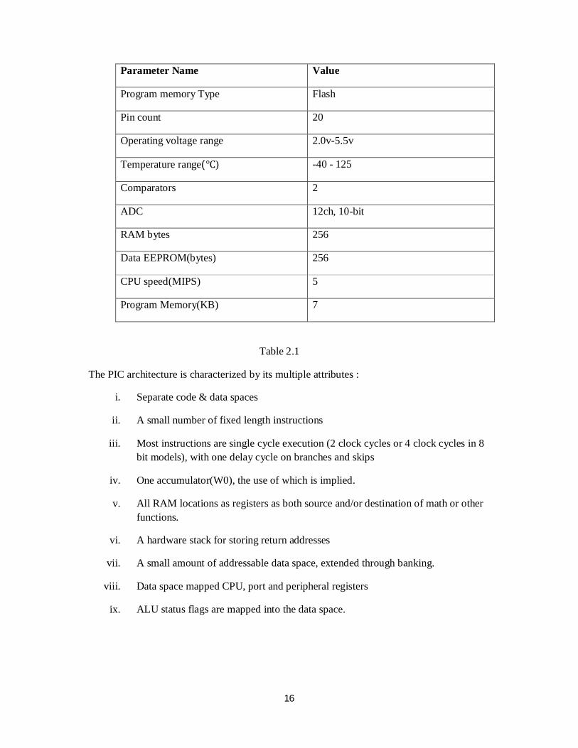
2.4 PIC16F690 The features of the PIC16F690 includes :
a) 4 channel PWM 10-bit
b) 256 bytes of EEPROM data memory
c) nanoWatt technology
d) 12-channels of 10-bit Analog-to-Digital Converter
e) Analog comparator module with two comparators
f) Programmable on-chip voltage reference
g) Auto-shutdown and restart options
h) Enhanced Low Power Timer 1
i) Timer 1 gate synch latch
16
Parameter Name Value
Program memory Type Flash
Pin count 20
Operating voltage range 2.0v-5.5v
Temperature range(℃) -40 - 125
Comparators 2
ADC 12ch, 10-bit
RAM bytes 256
Data EEPROM(bytes) 256
CPU speed(MIPS) 5
Program Memory(KB) 7
Table 2.1
The PIC architecture is characterized by its multiple attributes :
i. Separate code & data spaces
ii. A small number of fixed length instructions
iii. Most instructions are single cycle execution (2 clock cycles or 4 clock cycles in 8 bit models), with one delay cycle on branches and skips
iv. One accumulator(W0), the use of which is implied.
v. All RAM locations as registers as both source and/or destination of math or other functions.
vi. A hardware stack for storing return addresses
vii. A small amount of addressable data space, extended through banking.
viii. Data space mapped CPU, port and peripheral registers
ix. ALU status flags are mapped into the data space.

17
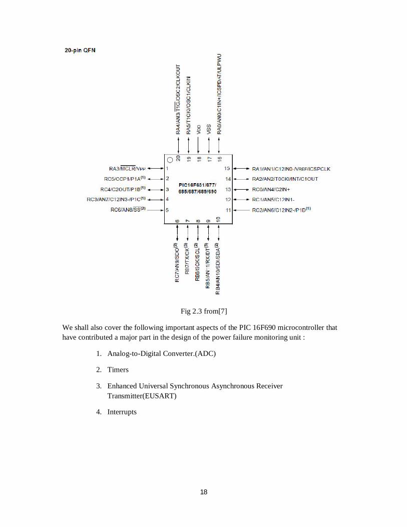
Fig 2.2 from[7]
The diagram below shows the pin structure of the PIC microcontroller.
The PIC16F690 consists of three ports namely :
a. PORTA- Pins 19,18,17,4,3,2
b. PORTB- Pins 13,12,11,10.
c. PORTC- pins 16,15,14,5,6,7,8,9.
A few key observations while looking at the pin out diagram of the above PIC 16F690 are:
i. Pins 1 and 20 act as the power supply and ground of the pic microcontroller.
ii. Pins 2 and 3 acts as the external oscillator pins.
iii. Pin 4 is the Master Clear pin
iv. Pins 10 and 12 can be configured as the transmitter and receiver pins respectively.
v. Pins 19 and 17 can be configured as the comparator1 input and output respectively
vi. Pins 16 and 6 can be configured as the comparator2 input and output respectively
vii. Pin 18 can be used as a Voltage reference when using the Analog to Digital Converter.
18
Fig 2.3 from[7]
We shall also cover the following important aspects of the PIC 16F690 microcontroller that have contributed a major part in the design of the power failure monitoring unit :
1. Analog-to-Digital Converter.(ADC)
2. Timers
3. Enhanced Universal Synchronous Asynchronous Receiver Transmitter(EUSART)
4. Interrupts

19
2.4.1 ANALOGUE-TO-DIGITAL CONVERTER Many applications require measurement of the analogue variables e.g voltage, temperature, pressure, speed etc. Since the microcontroller can only understand the digital language(1’s and 0’s), then we need an ADC for operation[1]
Selected PIC microcontrollers incorporate analogue inputs, which are connected to an ADC .The output of the ADC is a 10-bit binary representation of the input voltage[1].
Operation of the ADC in pic16f690
As mentioned above, the ADC allows conversion of an analog input signal to a 10-bit binary representation of that signal.
This device uses analog inputs, which are multiplexed into a single sample and hold circuit. Then the outputs of the sample & hold circuit is the input of the converter. The converter generates the 10-bit binary data by means of successive approximations and stores the conversion result in the ADC results register(ADRESL AND ADRESH).The ADC has a voltage reference that can either be connected to Vdd or a voltage connected to the external reference pins[7].
Fig 2.4 from[7]

20
ADC CONFIGURATION
The Analogue to Digital Converter need to be configured before being able to operate. The following are the steps that need to be understood first before anything else. These are:
i. PORT CONFIGURATION
When converting analog signals, the I/O pins should be configured for analog by setting the associated TRIS and ANSEL bits[7].
ii. CHANNEL SELECTION
This determines which channel is connected to the sample and hold circuit .
iii. ADC VOLTAGE REFERENCE
The VCFG bit of the ADCON0 register provides control of the positive voltage reference. The positive voltage reference can be either Vdd or an external voltage source[7].
iv. CONVERSION CLOCK
The source of the conversion clock can be selected via the ADCS bit of the ADCON1 register .[7]There are seven possible clock options :
Fosc/2
Fosc/4
Fosc/8
Fosc/16
Fosc/32
Fosc/64
Frc(dedicated internal oscillator).
v. INTERRUPT CONTROL
Upon completion of the analog-to-digital converter the ADC module allows for generation of an Interrupt.
This interrupt can be generated while the ADC is in operation or while in Sleep. Upon waking from Sleep, the next instruction following the SLEEP instruction is always executed[7].
vi. RESULTS FORMATTING

21
The 10-bit A/D conversion result can be supplied in two formats, left justified or right justified. The ADFM bit of the ADCON0 register controls the output format.
Fig 2.5 from [7]
The A/D Conversion procedure is as follows:
i. Configuration of the Port : This includes disabling pin output and configuring them as analog inputs.
ii. Configuration of the ADC module: -This will involve the Selection of the ADC conversion clock, configuring voltage reference, selecting the specific ADC input channel, selection of the result format(i.e left-justification or right justification ), and turning on the ADC module.
iii. Configuring the ADC interrupt(This is not a must): This will include the clearing of the ADC interrupt flag, enabling the ADC interrupts, enabling the peripheral interrupt bit, and lastly enabling global interrupt bit.
iv. Wait the required acquisition time
v. Starting the conversion by setting GO/DONE bit of the ADCON1 register.
vi. Waiting for ADC conversion to finish by : -Polling the GO/DONE bit
-Waiting for the ADC interrupts (if enabled)
viii. Reading the ADC Result
ix. Clearing the ADC Interrupt flag.
2.4.2 INTERRUPTS. Interrupts are powerful concept in embedded systems for controlling events in a time-critical environment. In a typical embedded system, the embedded processor (microcontroller) is responsible for doing more than one task (but can do only one at a time) [8]. Interrupts form the basis for separating the time-critical events from the others and execute them in a

22
prioritized manner. An interrupt tells the microcontroller to drop whatever it is doing and execute another program (the Interrupt Service Routine or ISR) stored at a predefined place in the program memory[6].
An interrupt is an asynchronous signal calling for processor attention. Interrupts can originate in hardware or in software. The interrupt mechanism is a way to avoid wasting processor time, since without interrupts code has to poll hardware devices in ineffective, closed loops. With interrupts, the processor can continue to do its work since the interrupt mechanism ensures the CPU receives a signal whenever an event occurs that requires its attention. PIC microcontrollers provide varying levels of support for interrupts[6].
The PIC microcontroller has the following sources of interrupts:
i. INT Pin Interrupt (external interrupt)
ii. TMR0 Overflow Interrupt
iii. PORTB Change Interrupt (pins RB7:RB4)
iv. Comparator Change Interrupt
v. Parallel Slave Port Interrupt
vi. USART Interrupts
vii. Receive Interrupt
viii. Transmit Interrupt
ix. A/D Conversion Complete Interrupt
x. LCD Interrupt.
xi. Data EEPROM Write Complete Interrupt
xii. Timer1 Overflow Interrupt
xiii. Timer2 Overflow Interrupt
xiv. CCP Interrupt
xv. SSP Interrupt
The register that is used in the control and status of the interrupt is the INTCON register.If the device has peripheral interrupts, there will be additional control registers to enable the peripheral interrupts and also hold the interrupt flag bits.These registers include PIE1, PIR1, PIE2, PIR2.
THE PIR1 AND PIR2 REGISTERS

23
These registers are helpful when you need to know the current state of PIC’s built-in peripherals devices e.g : -ADC
-EUSART Transmitter and receiver
-Comparators e.t.c
Reading the peripheral devices before they have finished their current processing gives a false result[10]. This is where the PIR registers come in and that is their importance. The PIR1 has 3 flags namely:
i. Bit<6> known as the ADIF which goes high when ADC conversion is completed
ii. Bit<5> known as RCIF which goes high when receiver buffer is full
iii. Bit<4> known as TXIF which goes high when the transmitter buffer is empty
PIR2 has 2 flags:
i. Bit<6> known as C2IF which goes high when the output of the comparator 2 has changed
ii. Bit<5> known as C1IF which goes high at a change in Comparator1[10].
INTCON REGISTER
This register is essential in the whole process of creating of interrupts. It controls the processing of interrupts[10]. The bits of interest are :
i. Bit<7>- GIE bit: The Global Interrupt Enable bit
a) Setting it enables all unmasked interrupts
b) Clearing it disables all the interrupts
ii. Bit<6>-PEIE bit: The Peripheral Interrupt Enable
a) Setting it enables peripheral interrupts
b) Clearing it disables peripheral interrupts
iii. Bit<5>-TOIE bit: TMR0 overflow interrupt enable bit
a) Setting it enables the TMR0 overflow interrupts
b) Clearing it disables the interrupt
iv. Bit<4>-INT bit:RB0 Interrupt Enable bit
a) Setting it enables the RA2 external interrupt

24
b) Clearing it disables the RA2 external interrupt
v. Bit<3>-RABIE bit-
a) Setting it enables interrupt-on-change in PortA&PortB
b) Clearing it disables interrupt-on-change
vi. Bit<2>-T0IF: TIMER0 Overflow Interrupt Flag bit
a) 1-TMR0 has overflowed
b) 0-TMR0 has not overflowed
vii. Bit<1>-INTF: RB0 External Interrupt Flag bit
a) 1-The RA2/INT external interrupt occurred
b) 0-The RA2/INT external interrupt did not occur
viii. Bit<0>-RABIF bit
a) 1-An interrupt-on-change in PortsA& B occurred
b) 0-An interrupt-on-change did not occur
2.4.3 TIMERS The PIC16F690 has in built timers for the function of timing and counting. A Timer module consists of three basic components for it to function. They include :
i. Source-a source signal is required. This can be either be a synchronous clock provided by an oscillator or a non-periodic event e.g. push of a button
ii. An 8-bit or 16-bit register in data memory to store the current value of the timer in binary. The value will increment depending on the selected edge of the signal transition
iii. A scaler-This can either be a pre-scaler(before the timer/counter value register) or a postscaler(after the timer/counter value register).It affects the input signal by dividing it by a specific value.

25
Fig 2.6
There are three types of timer modules associated with these microcontrollers namely :
i. Timer0 Module
ii. Timer1 Module
iii. Timer2 Module
Timer0 module
The Timer0 module is an 8-bit Timer/counter with the following features :
i. 8-bit timer/counter register
ii. 8-bit Prescaler (shared with the Watchdog Timer)
iii. Programmable internal or external clock source
iv. Programmable external clock-edge selection
v. Interrupt on overflow[7].
It can either be used as an 8-bit timer or an 8-bit counter. Both can be thought of as one and the same thing but the distinction lies from how the end result is used. To configure the Timer0 module, the OPTION_REG Special Function Register is used. The timer mode is selected by clearing the the T0CS bit of the OPTION register to ‘0’. Counter mode is selected by setting the T0CS bit of the OPTION register to ‘1’[8].
Timer1 module
The Timer1 module is a 16-bit timer/counter with the following features:
Source
Signal Pre-scaler
8-bit register in data memory to store
current value
Post-scaler

26
i. 16-bit timer/counter register pair(TMR1H:TMR1L)
ii. Programmable internal or external clock source
iii. 3-bit prescaler
iv. Optional LP oscillator
v. Wake-up on overflow(external clock, Asynchronous mode only)
vi. Interrupt on overflow
vii. Special Event Trigger (with ECCP)[8].
It’s a 16-bit incrementing counter which is accessed through the TMR1H:TMR1L register pair .Writing to these registers directly updates the module which acts mostly as a counter. When used as an internal clock source, it is used as a timer. If used a s an external clock source, It can be used as a timer or a counter[7].
Timer2 module
It has the following features :
i. 8-bit Timer register(TMR2)
ii. 8-bit period register(PR2)
iii. Interrupt on TMR2 match with PR2
iv. programmable prescaler
v. programmable postscaler
2.4.4 ENHANCED UNIVERSAL SYNCHRONOUS ASYNCHRONOUS RECEIVER TRANSMITTER Enhanced Universal Synchronous Asynchronous Receiver Transmitter or otherwise known as the (EUSART) is a serial I/O communications peripheral. It consists of clock generators, shift registers and data buffers necessary to execute an I/O serial data transfer independent of device program execution[7].There are two types of communication namely Serial and parallel communication .In serial communication transmitting and receiving of data in a stream of consecutive electric pulses that represent data or control codes are implemented. Serial communication can be divided into :
i. Synchronous serial communication
ii. Asynchronous serial communication
In Asynchronous Serial transmission, the information in a serial bit stream is contained in a time dependent waveform. Each bit code is transmitted for a fixed time period which is also known as the baud rate. The operation of a P16F690 can be described in a nutshell as follows-

27
The USART takes a byte of data and transmits it serially (one bit at a time) to the USART of the other PIC. The second USART receives the serial data bit by bit and assembles it into a byte that can be read from a register. The USART of the P16F690 is at RB7(pin10) and the input is at RB5(pin12).One USART waits for an indefinite period to receive the data signal from the other USART. The USART is controlled by the TXSTA register found in Bank 1 of the memory. An example of the settings normally used is :
TXSTA REGISTER
Bit7 Bit6 Bit5 Bit4 Bit3 Bit2 Bit1 Bit0
0 0 1 0 0 0 1 0
Bit 7-Not applicable in asynchronous mode
Bit 6-8 bit transmission
Bit 5-Enable transmission
Bit 4-asynchronous mode
Bit3-Break character bit disabled
Bit2-low speed
Bit1- 1 if the transmit shift register is empty and 0 if otherwise
Bit0-the 9th bit when used
To transmit a byte , we place it in the data register TXREG and set the bit ‘5’of the TXSTA. It is not necessary to set the Baud rate Control Register (BAUDCTL) , as we use the default asynchronous mode. After a short delay to allow data to be transmitted, the data is read from the RCREG register in the other pic microcontroller. To set up the USART of the other pic as a receiver, the RCSTA register is loaded as follows
RCSTA REGISTER
Bit 7 Bit6 Bit5 Bit4 Bit3 Bit2 Bit1 Bit0
1 0 0 1 0 0 0 0

28
Bit<7>=1 This bit enables the serial port when it is set
Bit<6>=0 8-bit reception
Bit<5> =0 not applicable
Bit<4>=1 enables receiver
Bit<3:0>=0 not applicable
2.5 LIQUID CRYSTAL DISPLAY An LCD is a small low cost display. It is easy to interface with a micro-controller because of an embedded controller(the black blob on the back of the board).The Liquid crystal display(LCD) is an electronic visual display, that uses the light modulating properties of liquid crystals which do not emit light directly. It is an electronically modulated optical device made up of any number of segments filled with liquid crystals and arrayed in front of a light source or reflector to produce images in monochrome or color.
LCD is actually a combination of two states of matter, that is the solid and the liquid. They retain their respective states with respect to another. Solids maintain their state unlike liquids which change their orientation. Liquid crystals are more heat sensitive than usual liquids in that a small amount of heat can easily turn the liquid crystal into a liquid hence the reason why they are used to make thermometers.
The power consumption of the LCD has made it very popular in the market. Unlike the LED power consumption which is in the order of milliwatts, the LCD power consumption is in the order of microwatts. It also has key advantages of having a low cost and good contrast. It is due to low power consumption that there is compatibility with the metal oxide semiconductor (MOS) integrated circuit. LCD’s are thin and flat, therefore are easily integrated into any electronic circuit with ease. Nevertheless, the LCD suffers from a number of disadvantages including short operating life, poor visibility in low ambient lighting, requirement of an alternating current (ac) drive, limited temperature range (between 0 and 100 degree Celsius), slow speed and need of light source.
BASIC CONCEPT BEHIND AN LCD
An LCD is comprised of rod shaped tiny molecules sandwiched between a flat piece of glass and a opaque substrate. These molecules in between the plates align into two separate physical positions based on the electric charge applied to them. When electric charge is applied they align to block the light entering through them, whereas when no charge is applied they become transparent. Light passing through makes the desired images appear.
LCD TYPES
There are various types and technologies of the Liquid Crystal Display. Some of the technologies include :

29
i. Blue Mode STN-this is simply a basic LCD with contrast ratio and viewing angle deficiencies.
ii. FSTN(Film STN)-It include additional linearization film so better the contrast
iii. CSTN(color STN)-It includes layers of color filters that have the capacity to create up to 65000 colors.
iv. DSTN(Double STN)-It has the added advantage of improving contrast and eliminating any other colors appearing on the screen.
It can also be divided into two:
Dynamic scattering display: When the display is energized, the molecules of energized areas of the display become turbulent and scatter light in all directions. As a result, the activated areas take on a frosted glass appearance resulting in a silver display. The unenergized areas of the display remain translucent.
Field Effect LCD: They contain front and back polarizers at right angle to each other. Without electric excitation, the light coming through the front polarizer is rotated 90° in the fluid
The types of LCD based on the displayed data include :
i. Segmented LCD Displays: These type of LCD’s display numbers, letters and fixed symbols. They were used in old style industrial panel display and situations where we needed to display a fixed number of characters.
ii. Graphical LCD Displays: These type of LCD, unlike the segmented LCD which consists of segments, contains pixels in rows and columns. By energizing a given set of pixels any character can be displayed.
iii. Color LCD Displays-These are divided into two types:
a. Passive Matrix - They apply the row and column approach and function by the application of a small bias to perpendicular lines of electrodes. The bias should be strong enough to darken bit at line section. It also uses multiplexed addressing scheme. One of its main drawbacks is that it can cause distortion
b. Active Matrix – They operate in such a way that each cell has its own thin film transistor or otherwise known TFT. The active matrix displays are addressed independently from behind the LCD. They use a direct addressing scheme. Some of its advantages are that it has a sharp display, better viewing angle, and 40:1 contrast. Some of its limitations is the complex hardware and the need for better backlight.

30
The structure of an LCD is as follows:
A liquid crystal cell consists of a thin layer (about 10 micrometers) of a liquid crystal sandwiched between two glass sheets with transparent electrodes deposited on their inside faces. The cell can either be reflective type (when one glass sheet is transparent and the other has a reflective coating) or transmittive type (when both glass sheets are transparent).An LCD does not have the capability of producing its own illumination. The fact of the matter is that it depends entirely on illumination falling on it from an external source from its visual effect.
Fig 2.7
KEY SPECIFICATIONS OF AN LCD
The factors that are important to look upon when examining or evaluating an LCD monitor are as follows:
i. Resolution- This is the horizontal and vertical size measured by the number of pixels
ii. Viewable size – This is the diagonal size of the LCD display panel
iii. Response time- The minimum time the LCD will take to change a pixel’s color or brightness
iv. Matrix Type-The matrix type can be either Active TFT or Passive
v. Brightness-This is also known as luminance. It is the amount of light emitted from the display.
vi. Contrast ratio- The ratio of the intensity of the brightest bright to the darkest dark
vii. Aspect ratio-This is the ratio of the width to the height
31
2.6 GSM/GPRS MODULE A GSM/GPRS module is a electronic piece of equipment used to establish communication between a computer and a GSM-GPRS network. Global System for Mobile communication (GSM) is an architecture used for mobile communication . Global Packet Radio Service (GPRS) is an extension of GSM that enables higher data transmission rate.
In the above project a GSM module has been used to send an sms to a remote mobile phone to notify the change in voltage fed to the ADC of the microcontroller. A Wireless MODEMs like other MODEM devices use serial communication to interface with and need Hayes compatible AT commands for communication with the computer (any microprocessor or microcontroller system).
A GSM requires a SIM (Subscriber Identity Module) card just like mobile phones to activate communication with the network. Also they have IMEI (International Mobile Equipment Identity) number similar to mobile phones for their identification. A GSM/GPRS MODEM can perform the following operations:
i. Make, Receive, or reject a voice call
ii. Read, add, search phonebook entries of the SIM
iii. Receive, send or delete SMS messages in a SIM.
The GSM communicates with the microcontroller through AT commands. This is done via serial communication. The AT commands are sent through the microcontroller. The modem then sends back a result after receiving the command. . Different AT commands supported by the MODEM can be sent by the microcontroller or any computer to interact with the GSM and GPRS cellular network.

32
Fig 2.8

33
CHAPTER 3: DESIGN
3.1 INTRODUCTION This chapter seeks to explain in depth the process used in the implementation and operation of the power failure monitoring unit which is PIC-microcontroller based. It also covers on the implementation of a measuring system for power attained from a simple power outlet of 240Volts. The power failure monitoring unit and power measuring system consists of two modules:
i. Software section
ii. Hardware section
In the Hardware section, it covers the various components used to build the power failure monitoring unit and the power measuring circuit. The circuit designs were done in Proteus software.
In the Software section, it shows the flowchart of the power failure monitoring unit and deals with the programming of the codes used to run the power failure monitoring unit and the power measuring system. Coding was done in assembly language and C language.
The power failure monitoring unit in a nutshell is as follows. We use three important peripherals in the microcontroller:
i. ADC
ii. UART
iii. TIMER/COUNTER
The voltage of the power outlet is 240 volts(AC) while the microcontroller is only able to accept 5v (dc).Therefore a circuit is needed to step down the voltage and rectify it to dc voltage so that the voltage is within the microcontroller range. Once a voltage of five volts has been attained, it is then fed to an ADC input of the microcontroller via a potentiometer where a threshold has been set. If there will be power loss, then it will automatically affect the voltage being fed to the ADC. Consequently, if the voltage being fed is not equal to five volts, then an LED will start to blink to show the loss of power. The start of an LCD timing device and the sending of an sms with the assistance of a GSM modem follow up to account for the time when there was loss of power and notification via mobile phone text message.
The power measuring system uses the Analog to Digital Converter of the microcontroller. A voltage supply of 5 volts is fed to the ADC of the pic 16F690 via a potentiometer and its equivalent reading observed from four 7-segment LEDs. The current is calculated by Ohm’s Law i.e. I=V/R .Once the current and voltage values are known, then the value of the power is given by: P=V*I.
34
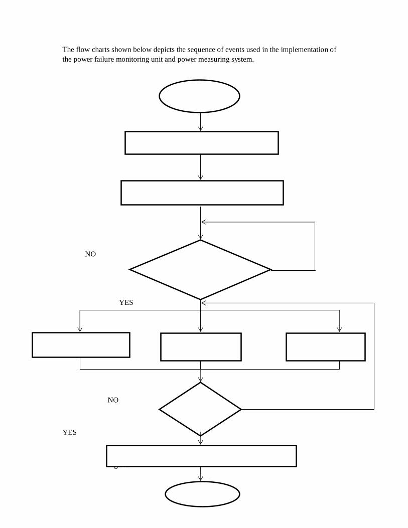
The flow charts shown below depicts the sequence of events used in the implementation of the power failure monitoring unit and power measuring system.
NO
YES
NO
YES
Fig 3.1
Initialization
Start
Check voltage levels
Is voltage < 5 volts or = zero?
LED blinking to show power loss
Start LCD Timer Send SMS to Mobile phone
Is voltage =5 volts?
TURN OFF LED, LCD TIMER AND GSM MODULE
End
35
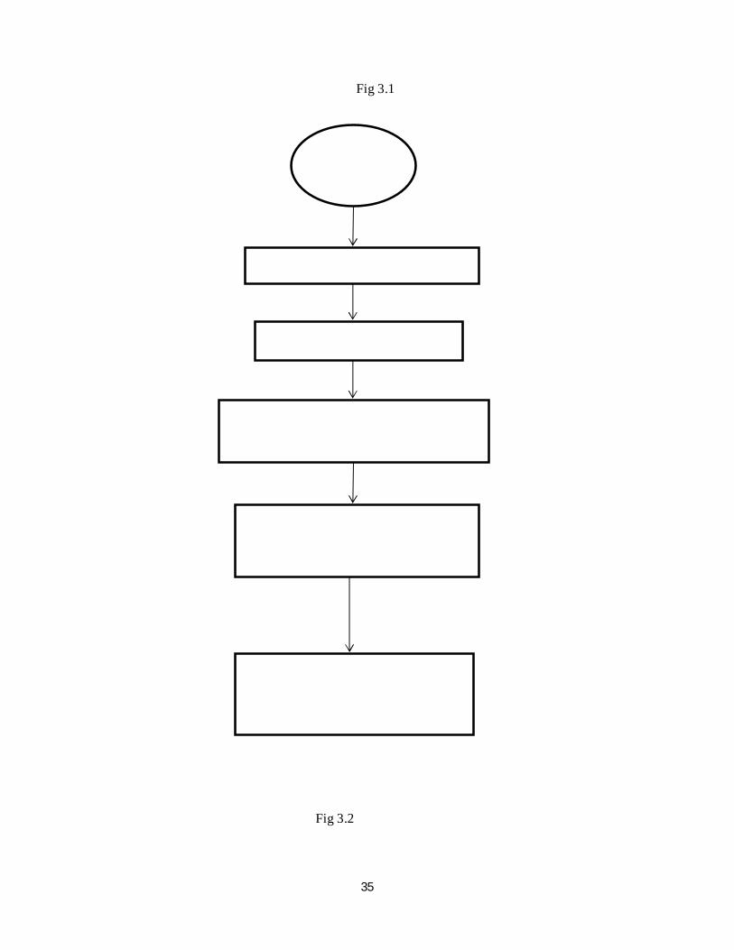
Fig 3.1
Fig 3.2
Start
Initialization
A-D Conversion
Display A-D Result on LED. This the voltage representation
Calculate current from Ohm’s law V=IR
R is the resistance of the potentiometer
Multiply the voltage value obtained by the current value measured to get power

36
3.2 HARDWARE SECTION In this section, the various components that have been used in the building of both the power failure monitoring unit and power measuring system are discussed. They are:
i. LCD module
ii. 7-Segment LED module
iii. Octal D-Type Transparent Latch
iv. GSM module
LCD module
An LCD is an electronic display module that is used to display a wide range of characters and numeric values. There are mainly two types of LCD’s. These are:
i. Alpha-numeric LCD
ii. Graphical LCD
Alphanumerical LCDs are limited to only showing simple alphabet and numeric displays while Graphical LCDs have the capacity to show alphanumeric, pictorial and graphical representation of data.An alphanumeric16x2 LCD display is one of the very basic common modules used in various electronic devices and circuits. Some of various reasons why they are preferred over the 7-Segment LED are:
i. They have no limitation in displaying special characters unlike the 7-segment LED
ii. They consume less power than the 7-Segment LEDs
iii. Economical
A 16x2 LCD means that it can display 16 characters per line. The total number of lines is 2. Each character is displayed in in 5x7 pixel matrix. The LCD pins are divided into Command pins(RS, E, RW) and data pins(D0-D7).
The Octal D-Type Transparent Latch
The Octal D-Type Transparent Latch is a Latch that uses D-Type Flip-Flops. It consists of eight latches with three state outputs that is normally used for bus organized system applications. The specific transparent latch that we used is the IC 74LS373 which is a 20-pin IC comprising of eight input data lines (D0-D7) and eight output lines (O0-O7). It also consists of an Output Enable pin (OE pin) and a Latch Enable pin (LE pin).

37
The IC 74LS373 consists of eight D-flip flops through which the input is given to each of the IC pins D0-D7.The flip flops appear transparent to the data(this means the flip flop data change asynchronously) when the Latch Enable pin(LE) is in HIGH state. The operation of the D type flip flop is that any input to the D pin at the present state will be given as the output in the next stage or next clock cycle e.g. if in the present state we have D=0 and Q=1, the next state will be D= anything and Q=0.
When the Latch Enable pin is pulled low, the data will be latched so that the data appears instantaneously providing a latching action. The work of the Output Enable is as follows: When the OE pin is LOW, the input data will appear in the output. But when the OE pin is HIGH, the output will be in a High Impedance State. Its advantages is that it has a high speed, a maximum operating voltage of 5volts, low power consumption, it is locally available since it is very popular in many types of electronic appliances.
7-Segment LED
A 7-segment display is the most basic electronic display device that can display digits from 0-9. They have numerous applications in devices that display numerical information. Examples of such devices are microwave ovens, digital clocks, digital score-boards etc.
The most common configuration has an array of eight LEDs arranged in a special pattern to display these digits. Every LED is assigned a name from ‘a’ to ‘h’ and is identified by its name. 7 LEDs ( ‘a’ –‘g’ ) are used to display numerals while the eighth LED ‘h’ is used to display the dot/decimal. It consists of a total of 10 pins. Eight pins correspond to the eight LEDs while the remaining two are internally shorted.
There are two types of 7-Segment LED configurations:
i. Common Cathode (CC)-This is where the negative terminals of all LEDs are connected to the common pins. The common is connected to the ground and a specific LED glows when its corresponding pin is given HIGH.
ii. Common Cathode (CA) –In this type of configuration, the common pin is given a HIGH logic and LED pins are given a LOW to display a number.
The advantages of LED displays is the size of the characters and the ability to be seen in dim light. They are also best suited for numbers.
GSM Module
GSM is an acronym that stands for Global System for Mobile Communications. It is a standard set developed by ETSI or the European Telecommunications Standards Institute to describe protocols for second generation(2G) digital cellular networks used by mobile phones.

38
A modem is a device which modulates and demodulates signals as required to meet the communication requirements. In the modulation stage, it modulates the carrier signal to encode digital information and in the Demodulation stage it demodulates an analog carrier signal to decode the transmitted information. Therefore a GSM modem modulates and demodulates GSM signals or 2G signals.
The SIM900 GSM modem is a quad band modem being able to operate in 850, 900, 1800, 1900 MHz bands and also offers improved GPRS functionalities useful in web enabled applications. The reason why the use of the SIM900 was preferred over other GSM modems e.g. SIM300 is because of its frequency bands since the SIM300 can only operate in 900,1800, and 1900 MHz . Furthermore some drawbacks of the SIM300 modem have been fixed in the SIM900 e.g. the appended HTTP/FTP features and range of reception. Its disadvantage is that it is more costly than the SIM300.
The figure below shows the schematic representation of the power failure monitoring unit.
Fig 3.2
RA0/AN0/C1IN+/ICSPDAT/ULPWU19
RB7/TX/CK10
RC0/AN4/C2IN+ 16
RC1/AN5/C12IN1- 15
RC2/AN6/C12IN2-/P1D 14
RC3/AN7/C12IN3-/P1C 7
RC4/C2OUT/P1B 6
RC5/CCP1/P1A 5
RC6/AN8/SS 8
RA4/AN3/T1G/OSC2/CLKOUT3
RA5/T1CKI/OSC1/CLKIN2
RB4/AN10/SDI/SDA13
RB5/AN11/RX/DT12
RB6/SCK/SCL11
RA1/AN1/C12IN0-/VREF/ICSPCLK18
RA3/MCLR/VPP4 RA2/AN2/T0CKI/INT/C1OUT17
RC7/AN9/SDO 9
U1
PIC16F690
R1330R
D1LED-RED
+5V
RXD
RTS
TXD
CTS
D7
14D
613
D5
12D
411
D3
10D
29
D1
8D
07
E6
RW5
RS
4
VSS
1
VD
D2
VEE
3
LCD1LM016L
100%
RV2
1k

39
The figure below shows the schematic representation of the power measuring system
3.3 SOFTWARE SECTION This chapter discusses the software environment that is used in the project. The software used in writing the codes are MPLAB and MikroC for assembly language and C language respectively.
MPLAB IDE is a Windows Operating System (OS) software program that runs on a PC to develop applications for Microchip microcontrollers and digital signal controllers. It is called an Integrated Development Environment, or IDE, because it provides a single integrated “environment” to develop code for embedded microcontrollers [4].The other programming software used is MikroC for PIC which is a full-featured ANSI C Compiler for PIC Devices from Microchip.
D[0
..15]
D03 Q0 2
D14 Q1 5
D27 Q2 6
D38 Q3 9
D413 Q4 12
D514 Q5 15
D617 Q6 16
D718 Q7 19
OE1
LE11
U2
74LS373
D03 Q0 2
D14 Q1 5
D27 Q2 6
D38 Q3 9
D413 Q4 12
D514 Q5 15
D617 Q6 16
D718 Q7 19
OE1
LE11
U3
74LS373
+5V
VSS
0%
RV1
1k
RA0/AN0/C1IN+/ICSPDAT/ULPWU19
RB7/TX/CK10
RC0/AN4/C2IN+ 16
RC1/AN5/C12IN1- 15
RC2/AN6/C12IN2-/P1D 14
RC3/AN7/C12IN3-/P1C 7
RC4/C2OUT/P1B 6
RC5/CCP1/P1A 5
RC6/AN8/SS 8
RA4/AN3/T1G/OSC2/CLKOUT3
RA5/T1CKI/OSC1/CLKIN2
RB4/AN10/SDI/SDA13
RB5/AN11/RX/DT12
RB6/SCK/SCL11
RA1/AN1/C12IN0-/VREF/ICSPCLK18
RA3/MCLR/VPP4 RA2/AN2/T0CKI/INT/C1OUT17
RC7/AN9/SDO 9
U1
PIC16F690PROGRAM=..\..\..\..\Users\Public\Documents\adc mwenda.HEX
D[0..15]

40
CHAPTER 4: RESULTS AND ANALYSIS
4.1 INTRODUCTION The following were the simulation results for both the power failure monitoring unit and the power measuring system. We were able to use Proteus Simulation which is a powerful software that enables compiling, debugging and simulating the project program very easily. It allows attachment of various devices to the microcontroller like switches, LCDs etc. and tests the performance of the code with the desired devices before the actual implementation of the project.
4.2 SIMULATION RESULTS The figure below shows the circuit used to implement the stepping down of 240v(AC) to 5V (DC).The circuit used in supplying the 5 volts was not used due to the cumulative expensive cost of all the components. Instead alternative and cheaper means of providing a constant supply of 5v(dc) was used. A mobile phone charger was used in this case.
.
T1
R1220Ω
R215kΩ
R31.5kΩ
C110µF
C210µF
U1LM117HVKSTL/883
Vout
ADJ
Vin
D1
1B4B42
1
2
4
3
V1
240 Vrms 50 Hz 0°
R4
800Ω
R51kΩ
XMM1

41
The Simulation results for the power failure monitoring unit were as follows:
Fig 4.1
The simulation results for the power measuring system and a table of power calculated are as follows:
Fig 4.2
RA0/AN0/C1IN+/ICSPDAT/ULPWU19
RB7/TX/CK10
RC0/AN4/C2IN+ 16
RC1/AN5/C12IN1- 15
RC2/AN6/C12IN2-/P1D 14
RC3/AN7/C12IN3-/P1C 7
RC4/C2OUT/P1B 6
RC5/CCP1/P1A 5
RC6/AN8/SS 8
RA4/AN3/T1G/OSC2/CLKOUT3
RA5/T1CKI/OSC1/CLKIN2
RB4/AN10/SDI/SDA13
RB5/AN11/RX/DT12
RB6/SCK/SCL11
RA1/AN1/C12IN0-/VREF/ICSPCLK18
RA3/MCLR/VPP4 RA2/AN2/T0CKI/INT/C1OUT17
RC7/AN9/SDO 9
U1
PIC16F690
R1330R
D1LED-RED
+5V
RXD
RTS
TXD
CTS
D7
14D
613
D5
12D
411
D3
10D
29
D1
8D
07
E6
RW5
RS4
VSS
1
VDD
2
VEE
3
LCD1LM016L
89%
RV2
1k
D[0
..15]
D03 Q0 2
D14 Q1 5
D27 Q2 6
D38 Q3 9
D413 Q4 12
D514 Q5 15
D617 Q6 16
D718 Q7 19
OE1
LE11
U2
74LS373
D03 Q0 2
D14 Q1 5
D27 Q2 6
D38 Q3 9
D413 Q4 12
D514 Q5 15
D617 Q6 16
D718 Q7 19
OE1
LE11
U3
74LS373
+5V
VSS
Volts+88.8
Volts+88.8
mA+88.8
72%
RV1
1k
RA0/AN0/C1IN+/ICSPDAT/ULPWU19
RB7/TX/CK10
RC0/AN4/C2IN+ 16
RC1/AN5/C12IN1- 15
RC2/AN6/C12IN2-/P1D 14
RC3/AN7/C12IN3-/P1C 7
RC4/C2OUT/P1B 6
RC5/CCP1/P1A 5
RC6/AN8/SS 8
RA4/AN3/T1G/OSC2/CLKOUT3
RA5/T1CKI/OSC1/CLKIN2
RB4/AN10/SDI/SDA13
RB5/AN11/RX/DT12
RB6/SCK/SCL11
RA1/AN1/C12IN0-/VREF/ICSPCLK18
RA3/MCLR/VPP4 RA2/AN2/T0CKI/INT/C1OUT17
RC7/AN9/SDO 9
U1
PIC16F690PROGRAM=..\..\..\..\Users\Public\Documents\adc mwenda.HEX
D[0..15]

42
Fig 4.3
The table below takes into account three sample voltages that were measured and compares them to their corresponding power values. It is clear that the power increases as the voltage tends to increase.Power is calculated as Voltage measured * Current calculated.
Current Calculated= Equivalent voltage measured/Resistance of Potentiometer
43
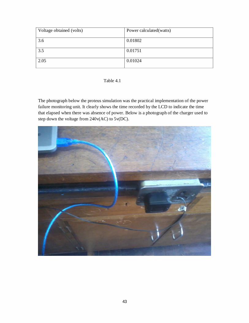
Voltage obtained (volts) Power calculated(watts)
3.6 0.01802
3.5 0.01751
2.05 0.01024
Table 4.1
The photograph below the proteus simulation was the practical implementation of the power failure monitoring unit. It clearly shows the time recorded by the LCD to indicate the time that elapsed when there was absence of power. Below is a photograph of the charger used to step down the voltage from 240v(AC) to 5v(DC).
44
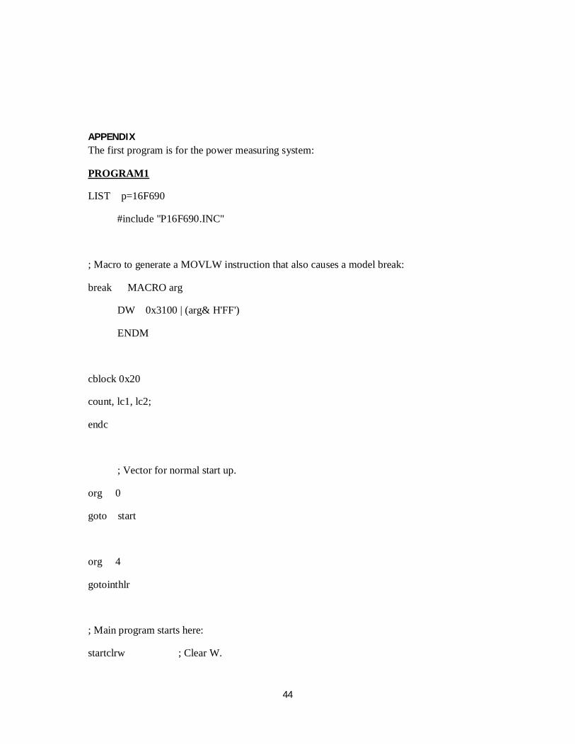
APPENDIX The first program is for the power measuring system:
PROGRAM1
LIST p=16F690
#include "P16F690.INC"
; Macro to generate a MOVLW instruction that also causes a model break:
break MACRO arg
DW 0x3100 | (arg& H'FF')
ENDM
cblock 0x20
count, lc1, lc2;
endc
; Vector for normal start up.
org 0
goto start
org 4
gotointhlr
; Main program starts here:
startclrw ; Clear W.

45
movwf PORTB ; Ensure PORTB is zero before we enable it.
movwf PORTC ; Ensure PORTD is zero before we enable it.
movwf count ; Reset count value.
movwf CCPR1H ; Clear.
movwf CCPR1L ; Clear.
; Set up ports:
bsf STATUS,RP0 ; Select Bank 1
movlw 0xFF ; Set W to mask for all inputs.
movwf TRISA ; set TRISA register as inputs.
movlw 0x00 ; Set W to mask for all inputs.
movwf TRISA ; set TRISA register as inputs.
bcf STATUS,RP0 ; Select Bank 1
bsf PORTA,0
bcf PORTA,0
bsf PORTA,0
bcf PORTA,0
bsf STATUS,RP0 ; Select Bank 0
movlw 0xFF ; Set W to mask for all inputs.
movwf TRISA ; set TRISA register as inputs.
clrf TRISB ; Set TRISB register as outputs.
clrf TRISC ; Set TRISD register as outputs.
movlw 0x81 ; ADFM=1, all inputs analogue, +VREF enabled.
movwf ADCON1 ; Save it.

46
bcf STATUS,RP0 ; Select Bank 0.
movlw 0xC1 ; Clock/Channel select and enable.
movwf ADCON0 ; Save it.
movlw 0x01 ; Number of loops of 255 clocks.
callswait ; Wait for acquire time.
do_convbsf ADCON0,GO
wait_eocbtfsc ADCON0,GO ; Is bit still set?
gotowait_eoc ; Yes, so loop and wait for end of conversion.
bcf STATUS,RP0 ; Ensure we have bank 0.
bsf PORTB,0 ; Show ISR in progress.
incfcount,F ; Increment count.
calldisp_adc ; Display captured value.
bcf PORTB,0 ; Remove progress bit.
movlw 0x40 ; Count
movwf count ; Save it.
loop1nop ; Dilly...
nop ; Dally...
nop ; Dilly...
decfsz count ; Decrement loop counter
goto loop1 ; Loop if no zero.
gotodo_conv ; Do another conversion.
disp_adcbsf STATUS,RP0 ; Bank 1.
47
movf ADRESL,W ; Get ADRESL into W.
bcf STATUS,RP0 ; Bank 0.
movwf PORTC ; Write it to port
bsf PORTB,4 ; Toggle latch enable
nop ; Wait
nop ; Wait
bcf PORTB,4 ; Toggle latch enable
movf ADRESH,W ; Get ADRESH into W.
movwf PORTC ; Write it to port
bsf PORTB,6 ; Toggle latch enable
nop ; Wait
nop ; Wait
bcf PORTB,6 ; Toggle latch enable
return
inthlrretfie
; -------------------------------------------------------------------------------
; Wait function
; -------------
swaitmovwf lc2
_sw2 movlw 0xFF
movwf lc1
_sw3 nop
decfsz lc1,f
goto _sw3
decfsz lc2,f
48
goto _sw2
return
END
PROGRAM2
The program was written in C language:
#define ADC_THRESHOLD 1000
unsignedintss,mm,hh;//time variables
unsignedintpower_failed,adc_value,sms_sent,led_on;
//this function initializes the PIC
voidmcu_init()
{
//ADC
ANSEL = 0x0F;
ANSELH = 0;
//LCD
TRISC=0;//configure portc as output
TRISB=0;
Lcd_Config(&PORTC,1,2,0, 7, 6, 5, 4);//initialize lcd with the given pins
Lcd_Cmd(LCD_CLEAR);//clear LCD

49
Lcd_Cmd(Lcd_CURSOR_OFF); // Turn cursor off
//usart
Usart_Init(9600);
}
//this function updates lcd with time value
voidupdate_lcd()
{
char s[3],m[3],h[3];
s[0] = (char)(ss/10 +'0');
s[1] = (char)(ss%10 +'0');
s[2] = '\0';
m[0] = (char)(mm/10 +'0');
m[1] = (char)(mm%10 +'0');
m[2] = '\0';
h[0] = (char)(hh/10 +'0');
h[1] = (char)(hh%10 +'0');
h[2] = '\0';
Lcd_out(1,4,h);
Lcd_chr(1,6,':');

50
Lcd_out(1,7,m);
Lcd_chr(1,9,':');
Lcd_out(1,10,s);
}
//this function sends string over USART
voidusart_str(char* csz_string)
{
// Loop until the end of string.
while (*csz_string != '\0') {
Usart_Write(*csz_string);
// Point to next character.
csz_string++;
}
}
//this function sends an sms
voidsend_sms(char *phone_no, char *msg)
{
usart_str("AT+CMGS=");
usart_str(phone_no);
delay_ms(1000);
usart_str("\r");

51
delay_ms(1000);
usart_str(msg);
delay_ms(1000);
Usart_Write(0x1A);
delay_ms(1000);
}
//the main function
void main()
{
mcu_init();//initialize LCD
PORTB.F4=0;//led off
led_on=0;
while(1)
{
adc_value = Adc_Read(2);//read ADC value
if(adc_value<ADC_THRESHOLD)//if power failure occured
{
power_failed=1;//indicates that failure occured
if(sms_sent==0)
{
//send sms

52
send_sms("1234567","POWER LOST");
sms_sent=1;//indicate that SMS has been sent
}
}
else //power available
{
//clear variables
power_failed=0;
sms_sent=0;
ss=mm=hh=0;
PORTB.F4=0;//led off
led_on=0;
}
if(power_failed)//if power failed
{
//toggle LED
if(led_on)
{
PORTB.F4=0;//led off
led_on=0;
}

53
else
{
PORTB.F4=1;//led on
led_on=1;
}
//update timer on LCD
if(++ss>59)//60 seconds
{
ss=0;
if(++mm>59) //60 minutes
{
mm=0;
if(++hh>11)
{
hh=0;
}
}
}
update_lcd();//update the time value on lcd
delay_ms(995);//some delay
}
}
}

54
BIBLIOGRAPHY
[1] M. Bates, Interfacing PIC Microcontrollers-Embedded Design by Interactive Simulation, London: Elsevier, 2006.
[2] N. Matic, PIC Microcontrollers for beginners.
[3] D. Smith, PIC in Practice, London: Elsevier, 2006.
[4] “Electronics Hub,” [Online]. Available: www.ElectronicsHub.com/Types & Applications of Microcontrollers. [Accessed 25 february 2014].
[5] M. P. Julio Sanchez, Microcontroller programming.The Microchip PIC, Florida: CRC Press, 2007.
[6] PIC16F631/677/685/687/689/690Datasheet, Microchip Technology Inc., 2007.
[7] H. W. Huang, PIC Microcontroller: An Introduction to Software and Hardware Interfacing, Delmar Learning, 2005.
[8] Timers:Timer0 Tutorial, Microchip Technology, 2007.
[9] O. Book, The Robot Builder's Cookbook, Elsevier , 2007.
[10] “allaboutcircuits,” [Online]. Available: www.allaboutcircuits/Forum?Embedded Systems & Microcontrollers. [Accessed 24 February 2014].