unit-i · baseband frequency range is called demodulation. • reasons for modulation: –...
TRANSCRIPT

UNIT-I
Amplitude Modulation System
1

Introduction to communications
• Elements of a communication system (cont)
2
Basic components Transmitter
– Convert Source (information) to signals– Send converted signals to the channel (by antenna if
applicable) Channel
– Wireless: atmosphere (free space)– Wired: coaxial cables, twisted wires, optical fibre
Receiver– Reconvert received signals to original information – Output the original information
m(t)
SignalProcessing
CarrierCircuits
Transmission Medium Carrier Circuits SignalProcessing
TRANSMITTER RECEIVERs(t) r(t)
)(ˆ tm
CHANNEL
Introduction to communications
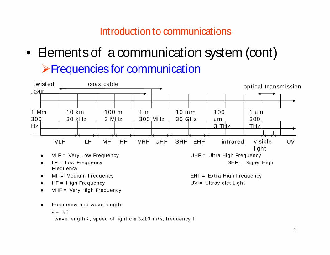
• Elements of a communication system (cont)Frequencies for communication
3
1 Mm300 Hz
10 km30 kHz
100 m3 MHz
1 m300 MHz
10 mm30 GHz
100 m3 THz
1 m300 THz
visible light
VLF LF MF HF VHF UHF SHF EHF infrared UV
optical transmissioncoax cabletwisted pair
VLF = Very Low Frequency UHF = Ultra High Frequency LF = Low Frequency SHF = Super High
Frequency MF = Medium Frequency EHF = Extra High Frequency HF = High Frequency UV = Ultraviolet Light VHF = Very High Frequency
Frequency and wave length: = c/f wave length , speed of light c 3x10⁸m/s, frequency f

Baseband vs Passband Transmission
• Baseband signals:– Voice (0-4kHz)– TV (0-6 MHz)
• A signal may be sent in its baseband format when a dedicated wiredchannel is available.
• Otherwise, it must be converted to passband.
4

Modulation: What and Why?
• The process of shifting the baseband signal to passband range is called Modulation.
• The process of shifting the passband signal to baseband frequency range is called Demodulation.
• Reasons for modulation:– Simultaneous transmission of several signals– Practical Design of Antennas– Exchange of power and bandwidth
5

Types of (Carrier) Modulation
• In modulation, one characteristic of a signal (generally a sinusoidal wave) known as the carrieris changed based on the information signal that we wish to transmit (modulating signal).
• That could be the amplitude, phase, or frequency, which result in Amplitude modulation (AM), Phase modulation (PM), or Frequency modulation (FM). The last two are combined as Angle Modulation
6

Types of Amplitude Modulation (AM)
• Double Sideband with carrier (we will call it AM): This is the most widely used type of AM modulation. In fact, all radio channels in the AM band use this type of modulation.
• Double Sideband Suppressed Carrier (DSBSC): This is the same as the AM modulation above but without the carrier.
• Single Sideband (SSB): In this modulation, only half of the signal of the DSBSC is used.
• Vestigial Sideband (VSB): This is a modification of the SSB to ease the generation and reception of the signal.
7
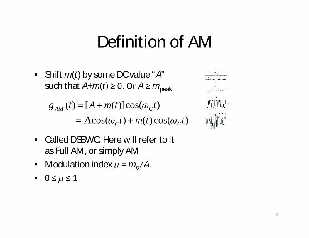
Definition of AM
• Shift m(t) by some DC value “A” such that A+m(t) ≥ 0. Or A ≥ mpeak
• Called DSBWC. Here will refer to it as Full AM, or simply AM
• Modulation index m = mp /A. • 0 ≤ m ≤ 1
)cos()()cos( )cos()]([)(
ttmtAttmAtg
CC
CAM
8
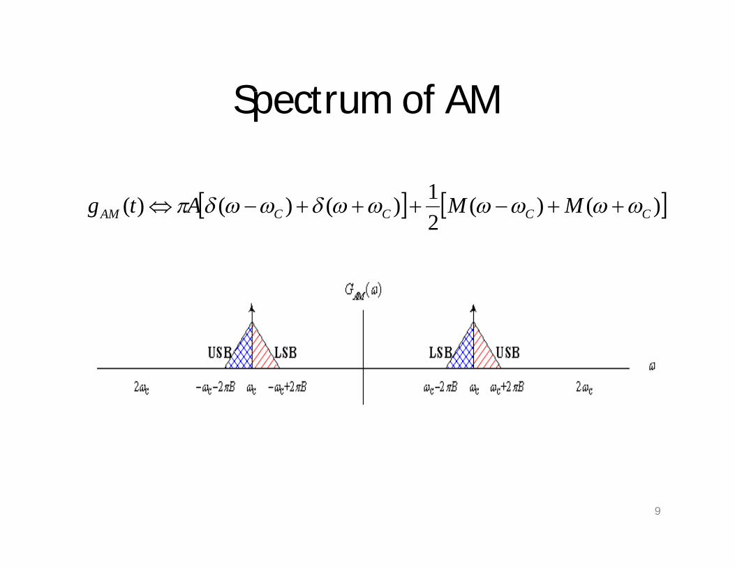
Spectrum of AM
)()(21)()()( CCCCAM MMAtg
9

Generation of AM
• AM signals can be generated by any DSBSC modulator, by using A+m(t) as input instead of m(t).
• In fact, the presence of the carrier term can make it even simpler. We can use it for switching instead of generating a local carrier.
• The switching action can be made by a single diode instead of a diode bridge.
10

AM Generator
• A >> m(t) (to ensure switchingat every period).
• vR=[cosct+m(t)][1/2 + 2/p(cosct-1/3cos3ct + …)]=(1/2)cosct+(2/p)m(t) cosct + other terms (suppressed by BPF)
• vo(t) = (1/2)cosct+(2/p)m(t) cosct
A
11
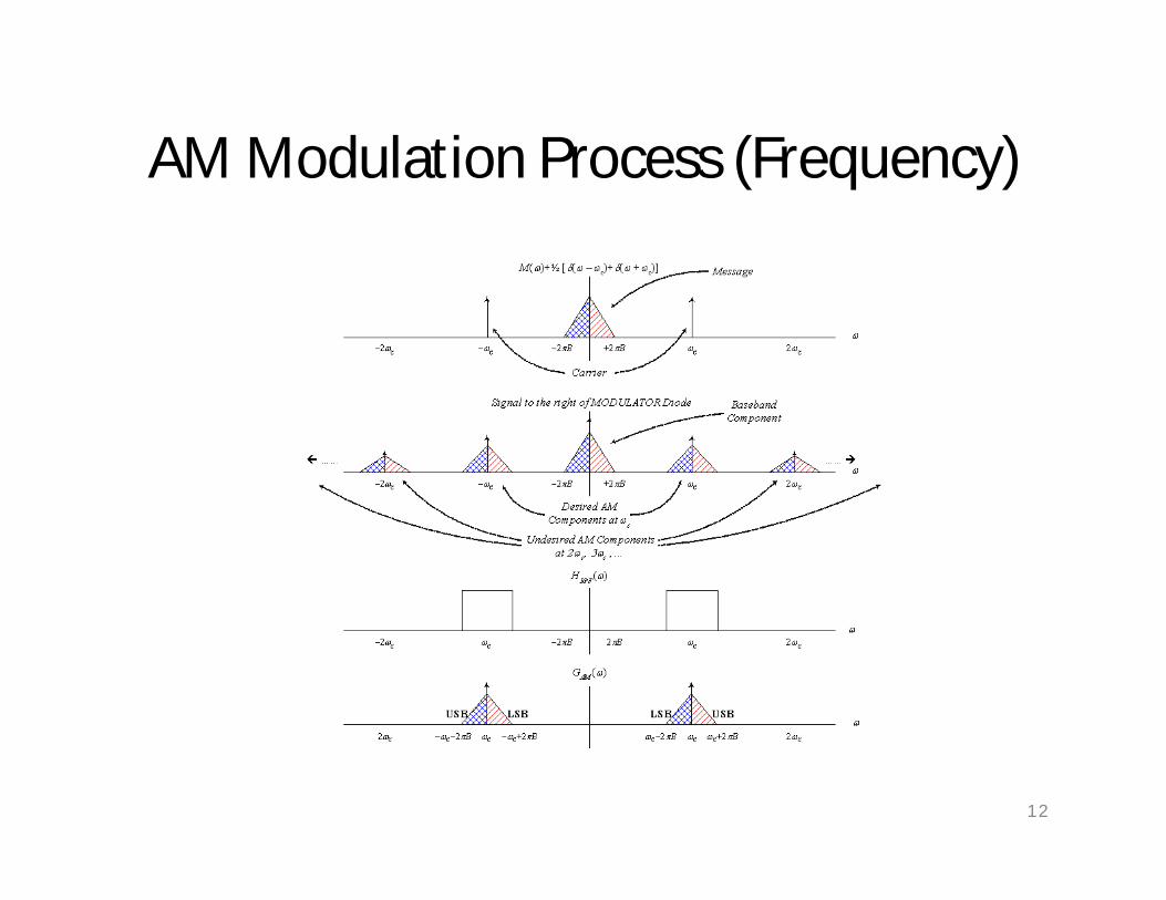
AM Modulation Process (Frequency)
12

AM Demodulation: Rectifier Detector
• Because of the presence of a carrier term in the received signal, switching can be performed in the same way we did in the modulator.
13

Rectifier Detector: Time Domain
14
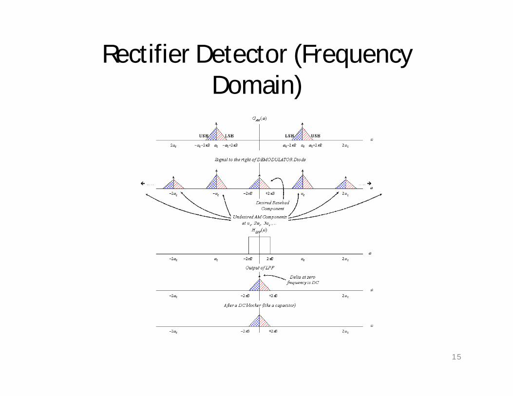
Rectifier Detector (Frequency Domain)
15

Envelope Detector
• When D is forward-biased, the capacitor charges and follows input.
• When D is reverse-biased, the capacitor discharges through R.
16

Double Sideband Suppressed Carrier (DSBSC)
DSBSC carrier is filtered or suppressed or receiver. That’s why it is called DSBSC
Problem with DSBSC1) Geometrical Carrier or Receiver2) Phase Detection Problem3) Frequency Shifting Properties
17

Time and Frequency Representation of DSBSC Modulation Process
18

DSBSC Demodulation
Double Sideband Suppressed Carrier (DSBSC)
For a broadcast system it is more economical to have one experience high power transmitter and expensive receiver, for such application a large carrier signal is transmitted along with the suppressed carrier modulated signal m(t) Cos (wct), thus no need to generate a local carrier. This is called AM in which the transmitted signal is.
Cos wct [ A + m(t) ]
19

Time and Frequency Representation of DSBSC Demodulation Process
20

Modulator Circuits
• Basically we are after multiplying a signal with a carrier.
• There are three realizations of this operation:– Multiplier Circuits– Non-Linear Circuits– Switching Circuits
21

Non-Linear Devices (NLD) • A NLD is a device whose input-output relation is non-
linear. One such example is the diode (iD=evD/vT).• The output of a NLD can be expressed as a power series
of the input, that isy(t) = ax(t) + bx2(t) + cx3(t) + …
• When x(t) << 1, the higher powers can be neglected, and the output can be approximated by the first two terms.
• When the input x(t) is the sum of two signal, m(t)+c(t), x2(t) will have the product term m(t)c(t)
22

Non-Linear Modulators
Undesired
C
UndesiredUndesired
C
Desired
C
UndesiredUndesired
CCC
CC
Undesired
C
UndesiredUndesired
C
Desired
C
UndesiredUndesired
CCC
CC
tbbtattbmtbmtam
tbttbmtbmtamtatmtbtmtaty
tbbtattbmtbmtam
tbttbmtbmtamtatmtbtmtaty
)2cos(22
)cos()cos()(2)()(
)(cos)cos()(2)()()cos(
)()cos()()cos()(
)2cos(22
)cos()cos()(2)()(
)(cos)cos()(2)()()cos(
)()cos()()cos()(
2
22
22
2
22
21
)()cos()()()()()cos()()()(
1
1
tmttmtctxtmttmtctx
C
C
Desired
C
Undesired
ttbmtamtytytz
)cos()(4)(2)()()( 21
23

Switching Modulators
• Any periodic function can be expressed as a series of cosines (Fourier Series).
• The information signal, m(t), can therefore be, equivalently, multiplied by any periodic function, and followed by BPF.
• Let this periodic function be a train of pulses.• Multiplication by a train of pulses can be
realized by simple switching.
24

Switching Modulator Illustration
25

Switching Modulator: Diode Bridge
26
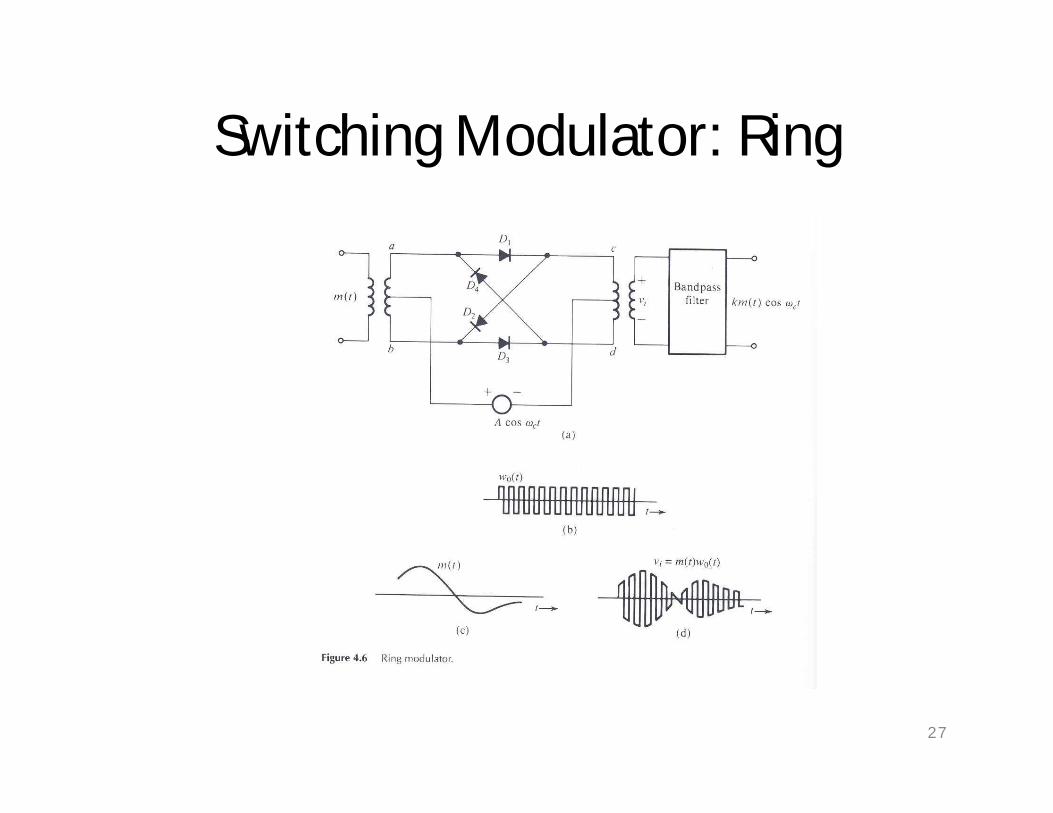
Switching Modulator: Ring
27

Demodulation of DSBSC
• The modulator circuits can be used for demodulation, but replacing the BPF by a LPF of bandwidth B Hz.
• The receiver must generate a carrier frequency in phase and frequency synchronization with the incoming carrier.
• This type of demodulation is therefore called coherentdemodulation (or detection).
X
c(t)
gDSBSC(t)e(t) HLPF( )
BW = 2 Bf(t)
DSBSC Demodulator (receiver)
28

From DSBSC to DSBWC (AM)
• Carrier recovery circuits, which are required for the operation of coherent demodulation, are sophisticated and could be quite costly.
• If we can let m(t) be the envelope of the modulated signal, then a much simpler circuit, the envelope detector, can be used for demodulation (non-coherent demodulation).
• How can we make m(t) be the envelope of the modulated signal?
29

Single-Side Band (SSB) Modulation
• DSBSC (as well as AM) occupies double the bandwidth of the baseband signal, although the two sides carry the same information.
• Why not send only one side, the upper or the lower?• Modulation: similar to DSBSC. Only change the settings
of the BPF (center frequency, bandwidth).• Demodulation: similar to DSBSC (coherent)
30

SSB Representation
How would we represent the SSB signal in the time domain?gUSB(t) = ?gLSB(t) = ?
31

Time-Domain Representation of SSB (1/2)
M() = M+() + M-()Let m+(t)↔M+() and m-(t)↔M-
() Then: m(t) = m+(t) + m-(t) [linearity]Because M+(), M-() are not even m+(t), m-(t) are complex.Since their sum is real they must beconjugates.m+(t) = ½ [m(t) + j mh(t)]m-(t) = ½ [m(t) - j mh(t)]What is mh(t) ?
32

Time-Domain Representation of SSB (2/2)
M() = M+() + M-() M+() = M()u(); M-() = M()u(-)sgn()=2u() -1 u()= ½ + ½ sgn(); u(-) = ½ -½ sgn()M+() = ½[ M() + M()sgn()]M-() = ½ [M() - M()sgn()]Comparing to:m+(t) = ½ [m(t) + j mh(t)] ↔ ½ [M() + j Mh()]m-(t) = ½ [m(t) - j mh(t)] ↔ ½ [M() - j Mh()]We findMh() = - j M()∙sgn() where mh(t)↔Mh()
33

Hilbert Transform• mh(t) is known as the Hilbert Transform (HT) of m(t).• The transfer function of this transform is given by:
H() = -j sgn()
• It is basically a /2 phase shifter
34

Hilbert Transform of cos(ct)
cos(ct) ↔ ( – c) + ( + c)]HT[cos(ct)] ↔ -j sgn() ( – c) + ( + c)]
= j sgn() ( – c) ( + c)]= j ( – c) + ( + c)]= j ( + c) - ( - c)] ↔ sin(ct)
Which is expected since:
cos(ct-/2) = sin(ct)
35

Time-Domain Operation for Hilbert Transformation
For Hilbert Transformation H() = -j sgn().What is h(t)?sgn(t) ↔ 2/(j) [From FT table]2/(jt) ↔ 2 sgn(-) [symmetry]1/( t) ↔ -j sgn()Since Mh() = - j M()∙sgn() = H() ∙ M()
Then
dtm
tmt
tmh
)(1
)(*1)(
36

)sin()()cos()(
)(21)(
21
)(21)(
21)(
)sin()()cos()(
)(21)(
21
)(21)(
21)(
ttmttm
etjmetm
etjmetmtg
ttmttm
etjmetm
etjmetmtg
ChC
tjh
tj
tjh
tjLSB
ChC
tjh
tj
tjh
tjUSB
CC
CC
CC
CC
)()()()()()(
CCLSB
CCUSB
MMGMMG
tjtjLSB
tjtjUSB
CC
CC
etmetmtg
etmetmtg
)()()(
)()()(
Finally …
37

Generation of SSB
• Selective Filtering MethodRealization based on spectrum analysis
• Phase-Shift MethodRealization based on time-domain expression of the modulated signal
38

Selective Filtering
39
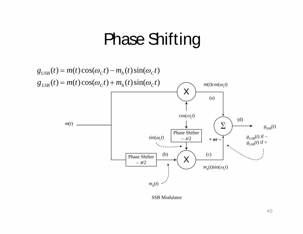
Phase Shifting
)sin()()cos()()()sin()()cos()()(
ttmttmtgttmttmtg
ChCLSB
ChCUSB
X
cos( ct)
SSB Modulator
X
sin( ct)Phase Shifter
– /2
Phase Shifter– /2
m(t)
mh(t)
mh(t)sin( ct)
m(t)cos( ct)
gSSB(t)
gUSB(t) if –gLSB(t) if ++ or –
(a)
(b) (c)
(d)
40

Phase-shifting Method:Frequency-Domain Illustration
41

SSB Demodulation (Coherent)
)(21 Output LPF
)2sin()(21)]2cos(1)[(
21)cos()(
)sin()()cos()()(
tm
ttmttmttg
ttmttmtg
ChCCSSB
ChCSSB
42

FDM in Telephony
• FDM is done in stages– Reduce number of carrier frequencies– More practical realization of filters
• Group: 12 voice channels 4 kHz = 48 kHzoccupy the band 60-108 kHz
• Supergroup: 5 groups 48 kHz = 240 kHzoccupy the band 312-552
• Mastergroup: 10 S-G 240 kHz = 2400 kHzoccupy the band 564-3084 kHz
43
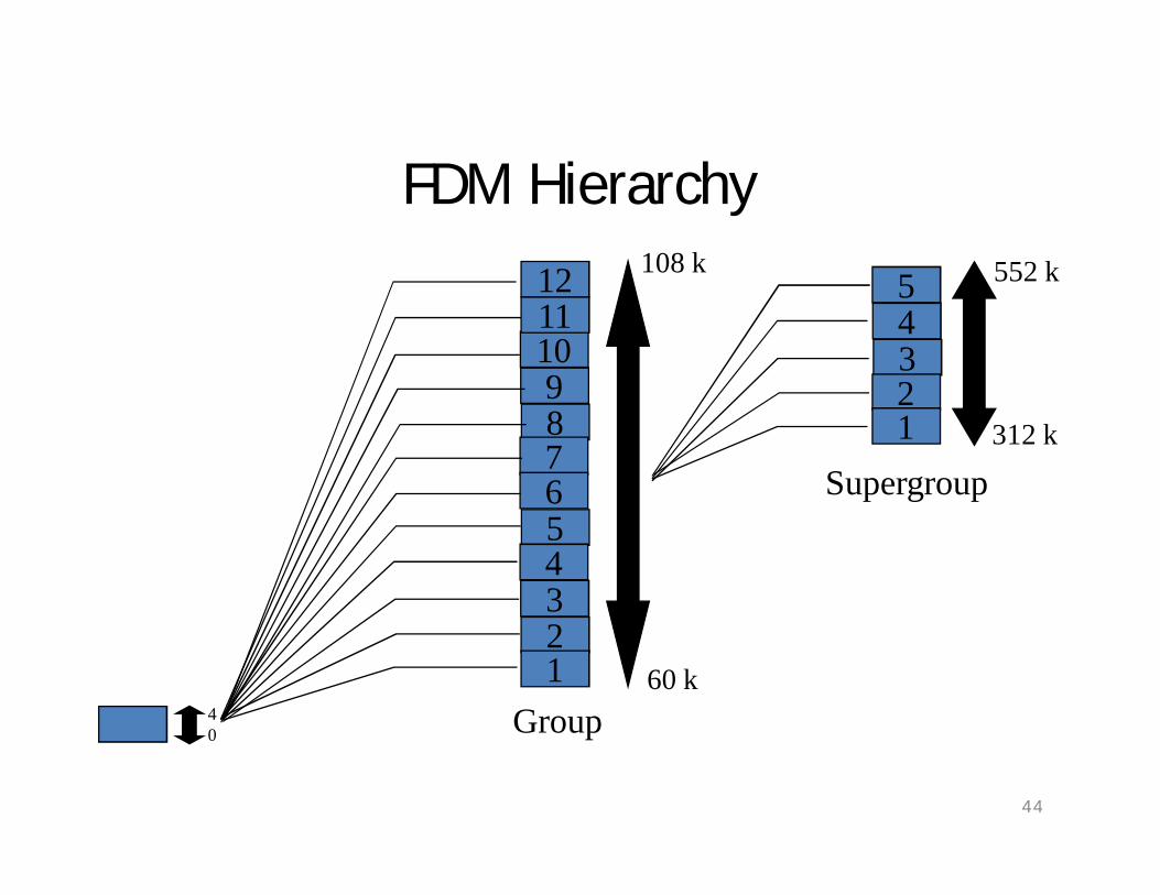
FDM Hierarchy
40
54321
109876
54321
1112
60 k
108 k
312 k
552 k
Group
Supergroup
44

Vestigial Side Band Modulation (VSB)
• What if we want to generate SSB using selective filtering but there is no guard band between the two sides?We will filter-in a vestige of the other band.
• Can we still recover our message, without distortion, after demodulation?Yes. If we use a proper LPF.
45

Filtering Condition of VSB
)cos()(2)( ttmtg CDSBSC
)()()( CCDSBSC MMG
)()()()( CCVSBVSB MMHG
C
C
at
C
baseband
CVSB
Basebandat
CCVSB
MMH
MMHX
2
2
)2()()(
)()2()()(
)()()()()( MHHHZ CVSBCVSBLPF
)()(1)(
CVSBCVSBLPF HH
H
; || ≤ 2 B
46
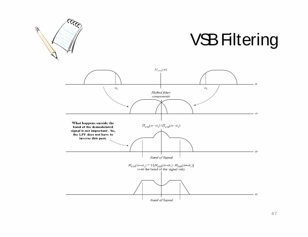
VSB Filtering
47

VSB Filter: Special Case
• Condition For distortionless demodulation:
• If we impose the condition on the filter at the modulator:
HVSB(-c) + HVSB(+c) = 1 ; || ≤ 2 B
Then HLPF = 1 for || ≤ 2 B (Ideal LPF)• HVSB() will then have odd symmetry around c over the
transition period.
)()(1)(
CVSBCVSBLPF HH
H
; || ≤ 2 B
48

49
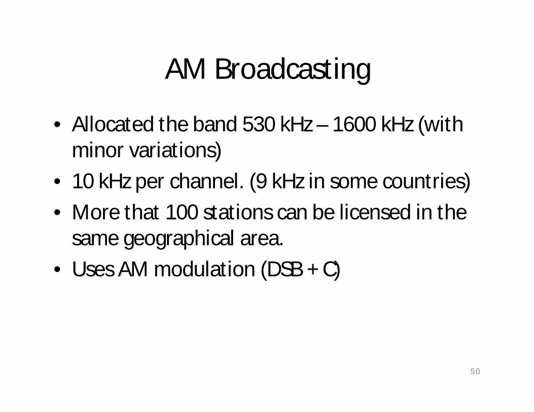
AM Broadcasting
• Allocated the band 530 kHz – 1600 kHz (with minor variations)
• 10 kHz per channel. (9 kHz in some countries)• More that 100 stations can be licensed in the
same geographical area. • Uses AM modulation (DSB + C)
50
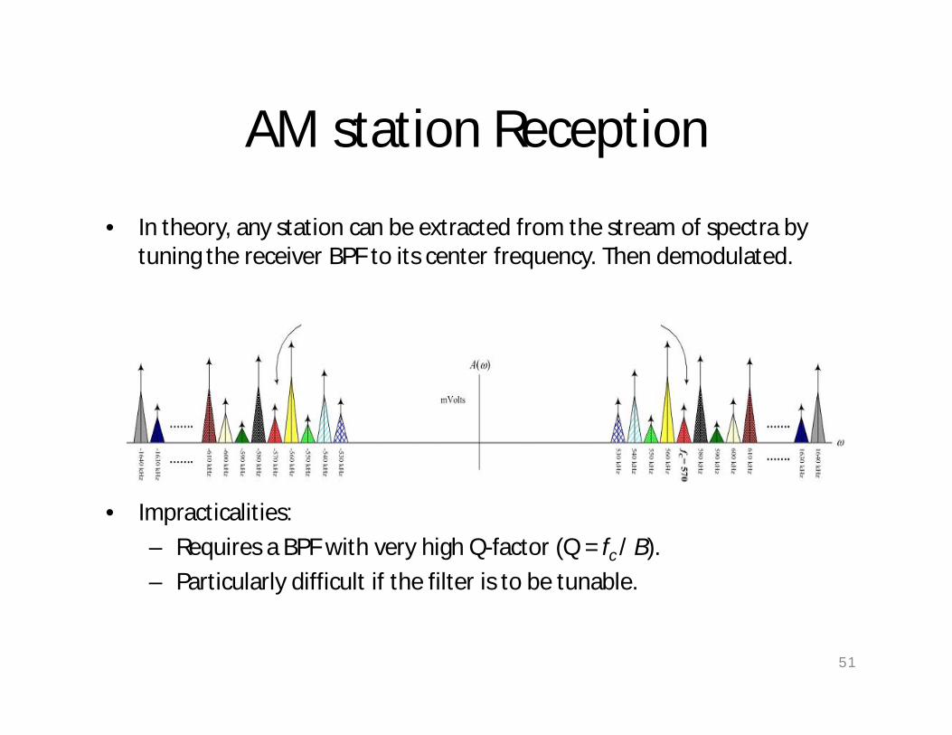
AM station Reception
• In theory, any station can be extracted from the stream of spectra by tuning the receiver BPF to its center frequency. Then demodulated.
• Impracticalities:– Requires a BPF with very high Q-factor (Q = fc / B).– Particularly difficult if the filter is to be tunable.
51

Angle Modulation – Frequency Modulation
Consider again the general carrier
represents the angle of the carrier.
There are two ways of varying the angle of the carrier.
a) By varying the frequency, c – Frequency Modulation.b) By varying the phase, c – Phase Modulation
1
) )cccc φ+tωV=tv cos
)cc φ+tω

Frequency Modulation
In FM, the message signal m(t) controls the frequency fc of the carrier. Consider the carrier
then for FM we may write:
FM signal ,where the frequency deviationwill depend on m(t).
Given that the carrier frequency will change we may write for an instantaneous carrier signal
where i is the instantaneous angle = and fi is the instantaneousfrequency. 2
) )tωV=tv ccc cos
) ) )t+fπV=tv ccs deviationfrequency 2cos
) ) )icicic φV=tπfV=tωV cos2coscos
tπf=tω ii 2

Frequency Modulation
Since then
i.e. frequency is proportional to the rate of change of angle.
If fc is the unmodulated carrier and fm is the modulating frequency, then we may deduce that
fc is the peak deviation of the carrier.
Hence, we have ,i.e.
3
tπf=φ ii 2 dtdφ
π=fπf=
dtdφ i
iii
21or 2
)dtdφ
π=tωΔf+f=f i
mcci 21cos
)tωΔf+f=dtdφ
π mcci cos
21 )tωπΔf+πf=
dtdφ
mcci cos22
Frequency Modulation
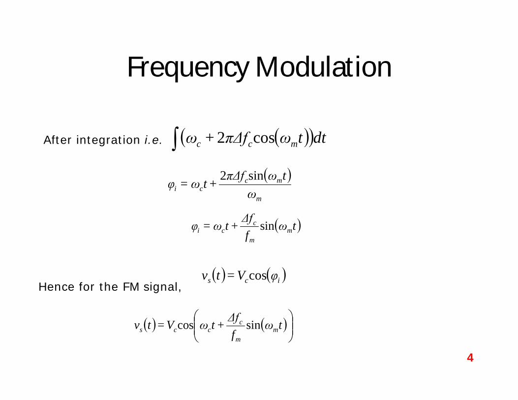
After integration i.e.
Hence for the FM signal,
4
) ) dttωπΔf+ω mcc cos2
)m
mcci ω
tωπΔf+tω=φ sin2
)tωfΔf+tω=φ m
m
cci sin
) )ics φV=tv cos
) )
tω
fΔf+tωV=tv m
m
cccs sincos
Frequency Modulation
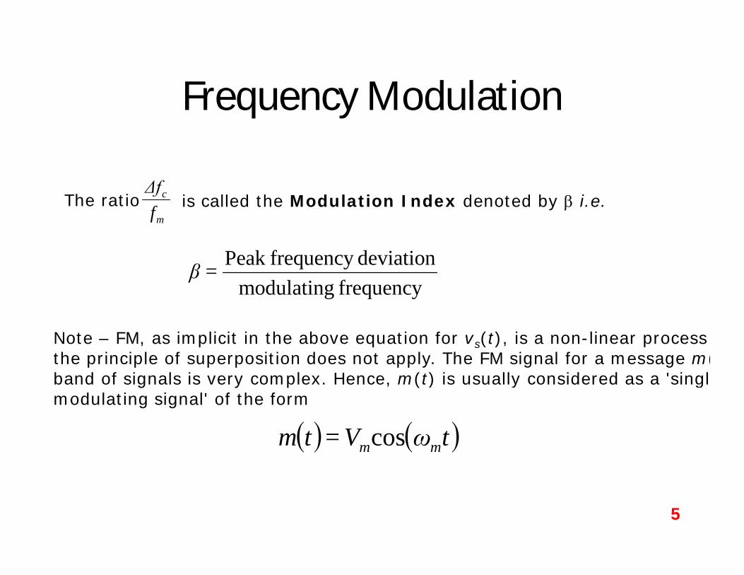
The ratio is called the Modulation Index denoted by i.e.
Note – FM, as implicit in the above equation for vs(t), is a non-linear process the principle of superposition does not apply. The FM signal for a message m(band of signals is very complex. Hence, m(t) is usually considered as a 'single tone modulating signal' of the form
5
frequency modulatingdeviationfrequency Peak =β
) )tωV=tm mmcos
m
c
fΔf

Frequency Modulation
The equation may be expressed as Bessel
series (Bessel functions)
where Jn() are Bessel functions of the first kind. Expanding the equation for a few terms we have:
tJVtJV
tJVtJVtJVtv
mcmc
mcmcc
ff
mcc
ff
mcc
ff
mcc
ff
mccf
ccs
2Amp
2
2Amp
2
Amp
1
Amp
1
Amp
0
)2(cos)()2(cos)(
)(cos)()(cos)()(cos)()(
6
) )
tω
fΔf+tωV=tv m
m
cccs sincos
) ) )
=nmcncs tnω+ωβJV=tv cos

FM Signal Spectrum.
The image cannot be displayed. Your computer may not have enough memory to open the image, or the image may have been corrupted. Restart your computer, and then open the file again. If the red x still appears, you may have to delete the image and then insert it again.
The amplitudes drawn are completely arbitrary, since we have not found any value for Jn() – this sketch is only to illustrate the spectrum.
7
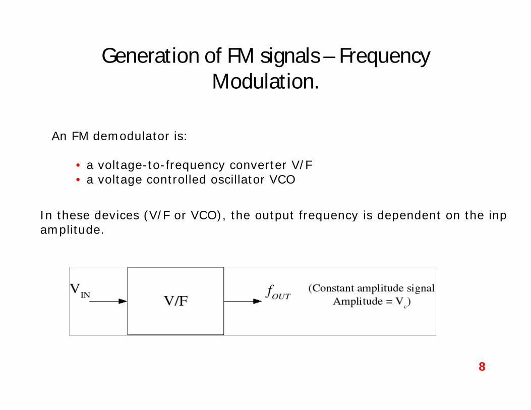
Generation of FM signals – Frequency Modulation.
An FM demodulator is:
• a voltage-to-frequency converter V/F• a voltage controlled oscillator VCO
In these devices (V/F or VCO), the output frequency is dependent on the input voltage amplitude.
The image cannot be displayed. Your computer may not have enough memory to open the image, or the image may have been corrupted. Restart your computer, and then open the file again. If the red x still appears, you may have to delete the image and then insert it again.
8

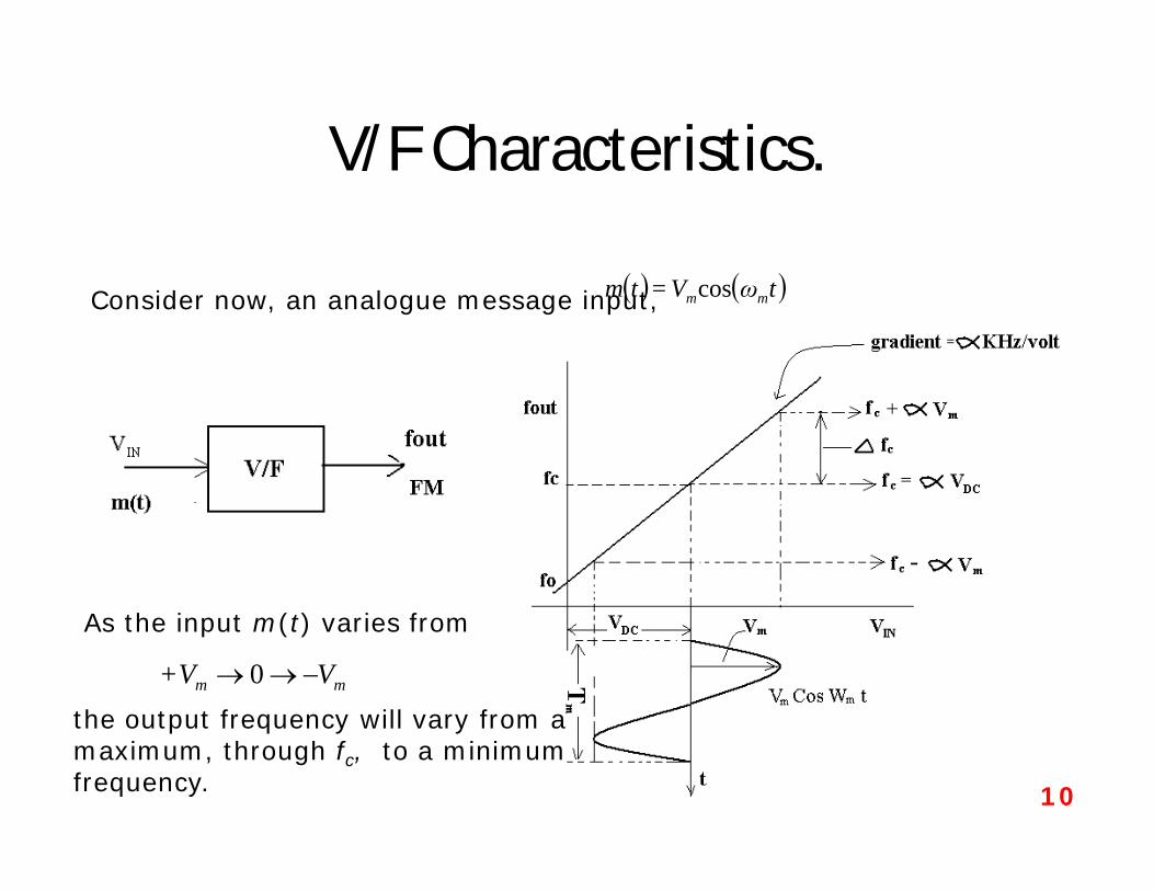
V/F Characteristics.
Apply VIN , e.g. 0 Volts, +1 Volts, +2 Volts, -1 Volts, -2 Volts, ... and measure the frequency output for each VIN . The ideal V/F characteristic is a straight line as shown below.
The image cannot be displayed. Your computer may not have enough memory to open the image, or the image may have been corrupted. Restart your computer, and then open the file again. If the red x still appears, you may have to delete the image and then insert it again.
fc, the frequency output when the input is zero is called the undeviated or nominal carrier frequency.
The gradient of the characteristic The image cannot be displayed. Your computer may not have enough memory to open the image, or the image may have been corrupted. Restart your computer, and then open the file again. If the red x still appears, you may have to delete the image and then insert it again.
ΔVΔf
is called the Frequency Conversion Factordenoted by per Volt.
9
V/F Characteristics.
Consider now, an analogue message input,
As the input m(t) varies from
the output frequency will vary from a maximum, through fc, to a minimum frequency. 10
) )tωV=tm mmcos
mm VV+ 0

V/F Characteristics.
For a straight line, y = c + mx, where c = value of y when x = 0, m = gradient, hence we may say
and when VIN = m(t) ,i.e. the deviation depends on m(t).
Considering that maximum and minimum input amplitudes are +Vm and -Vmrespectively, then
on the diagram on the previous slide.
The peak-to-peak deviation is fmax – fmin, but more importantly for FM the peak deviation fc is
Peak Deviation, Hence, Modulation Index, 11
INOUT αV+f=f c
)tαm+f=f cOUT
mc
mc
αVf=fαV+f=f
min
max
mc αV=Δfm
m
m
c
fαV=
fΔf=β

Summary of the important points of FM
• In FM, the message signal m(t) is assumed to be a single tone frequency,
• The FM signal vs(t) from which the spectrum may be obtained as
where Jn() are Bessel coefficients andModulation Index,
• Hz per Volt is the V/F modulator, gradient orFrequency Conversion Factor,
per Volt
• is a measure of the change in output frequency for a change in input amplitude.
Peak Deviation (of the carrier frequency from fc) 12
) )tωV=tm mmcos
) ) )
=nmcncs tnω+ωβJV=tv cos
m
m
m
c
fαV=
fΔf=β
mc αV=Δf
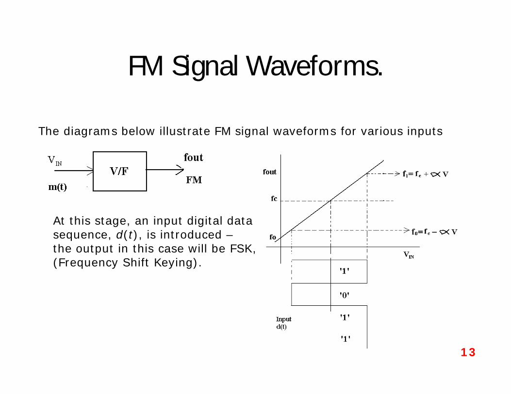
FM Signal Waveforms.
The diagrams below illustrate FM signal waveforms for various inputs
At this stage, an input digital datasequence, d(t), is introduced –the output in this case will be FSK,(Frequency Shift Keying).
13

FM Signal Waveforms.
Assuming s0'for s1'for )(
VVtd
s0'for s1'for
0
1
VfffVfff
cOUT
cOUT
the output ‘switches’
between f1 and f0.
14
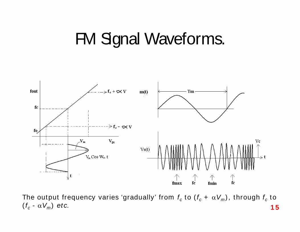
FM Signal Waveforms.
The output frequency varies ‘gradually’ from fc to (fc + Vm), through fc to (fc - Vm) etc. 15
FM Signal Waveforms.
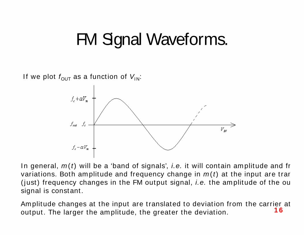
If we plot fOUT as a function of VIN:
In general, m(t) will be a ‘band of signals’, i.e. it will contain amplitude and frequency variations. Both amplitude and frequency change in m(t) at the input are translated to (just) frequency changes in the FM output signal, i.e. the amplitude of the output FM signal is constant.
Amplitude changes at the input are translated to deviation from the carrier at the output. The larger the amplitude, the greater the deviation. 16

FM Signal Waveforms.
Frequency changes at the input are translated to rate of change of frequency at the output.An attempt to illustrate this is shown below:
17
FM Spectrum – Bessel Coefficients.
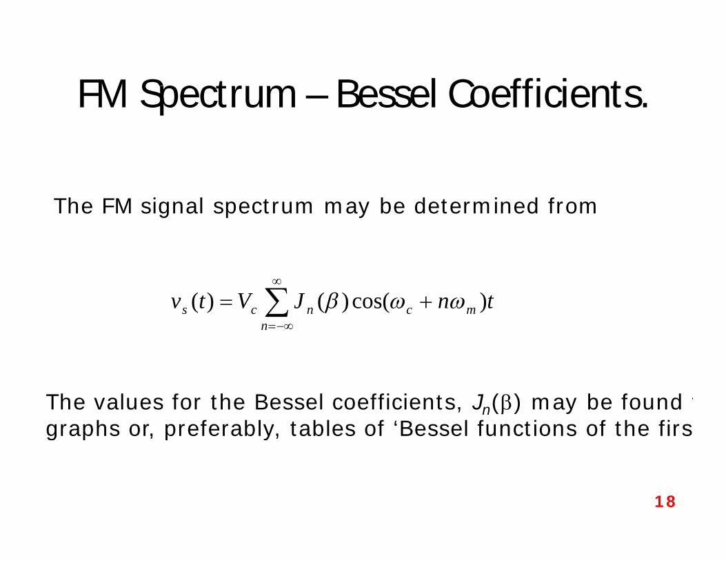
The FM signal spectrum may be determined from
n
mcncs tnJVtv )cos()()(
The values for the Bessel coefficients, Jn() may be found from graphs or, preferably, tables of ‘Bessel functions of the first kind’.
18

FM Spectrum – Bessel Coefficients.
In the series for vs(t), n = 0 is the carrier component, i.e. )cos()(0 tJV cc , hence the n = 0 curve shows how the component at the carrier frequency, fc, varies in amplitude, with modulation index .
19
Jn()
= 2.4 = 5

FM Spectrum – Bessel Coefficients.
Hence for a given value of modulation index , the values of Jn() may be read off the graph and hence the component amplitudes (VcJn()) may be determined.
A further way to interpret these curves is to imagine them in 3 dimensions
20

Examples from the graph
= 0: When = 0 the carrier is unmodulated and J0(0) = 1, all other J
= 2.4: From the graph (approximately)
J0(2.4) = 0, J1(2.4) = 0.5, J2(2.4) = 0.45 and J3(2.4) = 0.2
21

Significant Sidebands – Spectrum.
As may be seen from the table of Bessel functions, for values of n above a certain value, the values of Jn() become progressively smaller. In FM the sidebands are considered to be significant if Jn() 0.01 (1%).
Although the bandwidth of an FM signal is infinite, components with amplitudes VcJn(), for which Jn() < 0.01 are deemed to be insignificant and may be ignored.
Example: A message signal with a frequency fm Hz modulates a carrier fc to produce FM with a modulation index = 1. Sketch the spectrum.
n Jn(1) Amplitude Frequency 0 0.7652 0.7652Vc fc 1 0.4400 0.44Vc fc+fm fc - fm 2 0.1149 0.1149Vc fc+2fm fc - 2fm 3 0.0196 0.0196Vc fc+3fm fc -3 fm 4 0.0025 Insignificant 5 0.0002 Insignificant
22

Significant Sidebands – Spectrum.
As shown, the bandwidth of the spectrum containing significant components is 6fm, for = 1.
23

Significant Sidebands – Spectrum.
The table below shows the number of significant sidebands for various modulation indices () and the associated spectral bandwidth.
No of sidebands 1% of unmodulated carrier
Bandwidth
0.1 2 2fm 0.3 4 4fm 0.5 4 4fm 1.0 6 6fm 2.0 8 8fm 5.0 16 16fm
10.0 28 28fm e.g. for = 5,
16 sidebands (8 pairs).
24

Carson’s Rule for FM Bandwidth.
An approximation for the bandwidth of an FM signal is given byBW = 2(Maximum frequency deviation + highest modulated frequency)
)(2Bandwidth mc ff Carson’s Rule
25
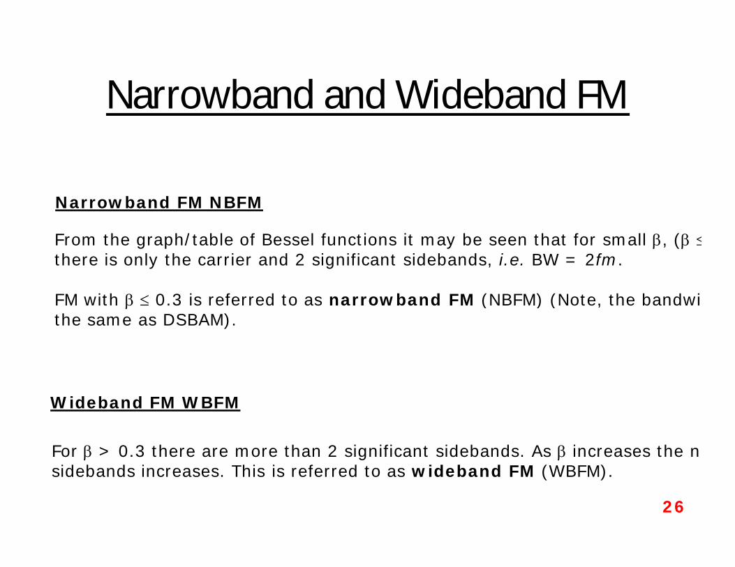
Narrowband and Wideband FM
From the graph/table of Bessel functions it may be seen that for small , ( there is only the carrier and 2 significant sidebands, i.e. BW = 2fm.
FM with 0.3 is referred to as narrowband FM (NBFM) (Note, the bandwidth is the same as DSBAM).
For > 0.3 there are more than 2 significant sidebands. As increases the number of sidebands increases. This is referred to as wideband FM (WBFM).
Narrowband FM NBFM
Wideband FM WBFM
26

VHF/FM
mc Vf
VHF/FM (Very High Frequency band = 30MHz – 300MHz) radio transmissions, in the band 88MHz to 108MHz have the following parameters:
Max frequency input (e.g. music) 15kHz fm
Deviation 75kHz
Modulation Index 5 m
c
ff
For = 5 there are 16 sidebands and the FM signal bandwidth is 16fm = 16 x 15kHz= 240kHz.Applying Carson’s Rule BW = 2(75+15) = 180kHz.
27

Comments FM
• The FM spectrum contains a carrier component and an infinite number of sidebands at frequencies fc nfm (n = 0, 1, 2, …)
FM signal,
n
mcncs tnJVtv )cos()()(
• In FM we refer to sideband pairs not upper and lower sidebands. Carrier or other components may not be suppressed in FM.
• The relative amplitudes of components in FM depend on the values Jn(), where
m
m
fV
thus the component at the carrier frequency depends on m(t), as do all the
other components and none may be suppressed.28
Comments FM
• Components are significant if Jn() 0.01. For <<1 ( 0.3 or less) only JJ1() are significant, i.e. only a carrier and 2 sidebands. Bandwidth is 2fm, similar to DSBAM in terms of bandwidth - called NBFM.
• Large modulation index m
c
ff
means that a large bandwidth is required – called
WBFM.
• The FM process is non-linear. The principle of superposition does not apply. When m(t) is a band of signals, e.g. speech or music the analysis is very difficult (impossible?). Calculations usually assume a single tone frequency equal to themaximum input frequency. E.g. m(t) band 20Hz 15kHz, fm = 15kHz is used.
29
Power in FM Signals.
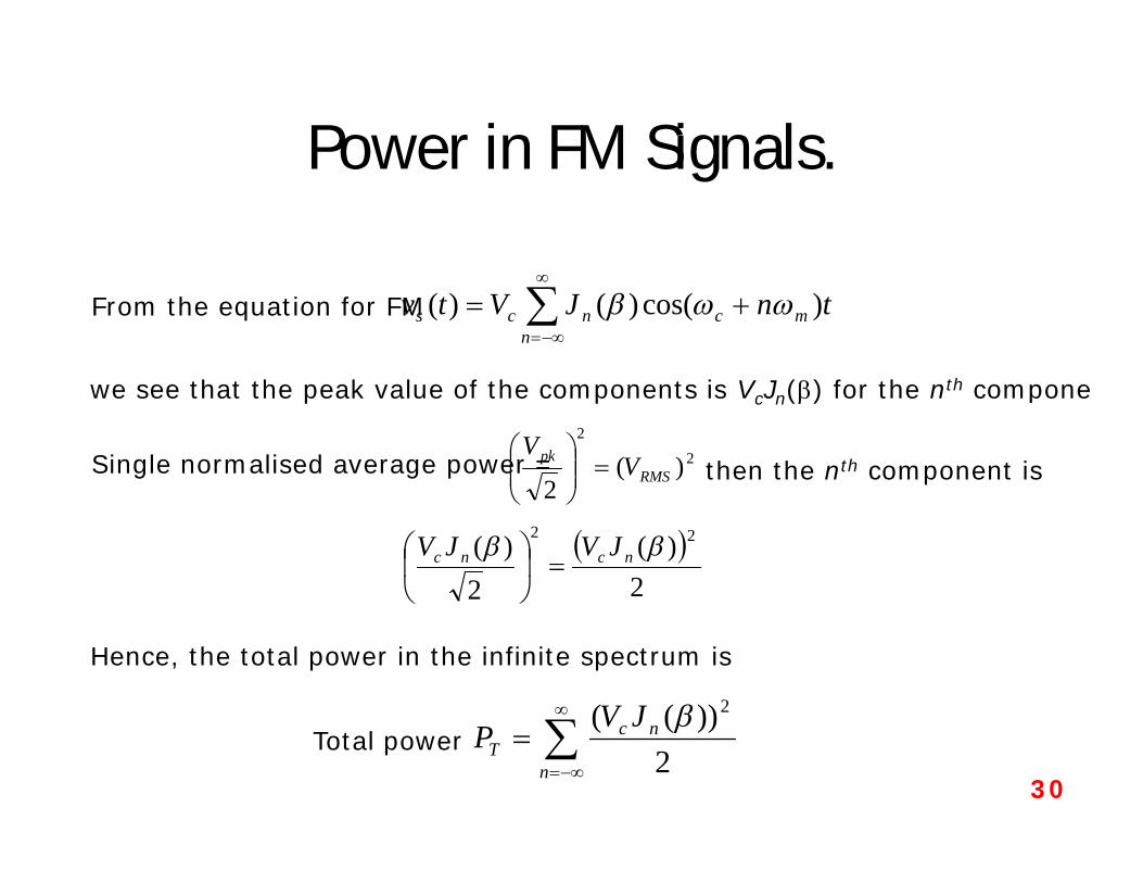
From the equation for FM
n
mcncs tnJVtv )cos()()(
we see that the peak value of the components is VcJn() for the nth component.
Single normalised average power = 22
)(2 RMSpk V
V
then the nth component is
)2
)(2
)( 22 ncnc JVJV
Hence, the total power in the infinite spectrum is
Total power
n
ncT
JVP
2))(( 2
30

Power in FM Signals.
By this method we would need to carry out an infinite number of calculations to find PT. But, considering the waveform, the peak value is Vc, which is constant.
Since we know that the RMS value of a sine wave is 22
2
cpk VV
and power = (VRMS)2 then we may deduce that )
n
ncccT
JVVVP
2)(
22
222
Hence, if we know Vc for the FM signal, we can find the total power PT for the infinite spectrum with a simple calculation. 31
Power in FM Signals.
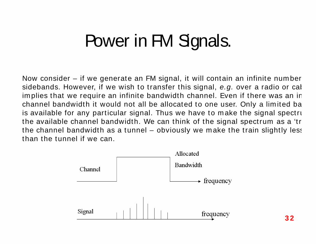
Now consider – if we generate an FM signal, it will contain an infinite number of sidebands. However, if we wish to transfer this signal, e.g. over a radio or cable, this implies that we require an infinite bandwidth channel. Even if there was an infinite channel bandwidth it would not all be allocated to one user. Only a limited bandwidthis available for any particular signal. Thus we have to make the signal spectrum fit intothe available channel bandwidth. We can think of the signal spectrum as a ‘train’ and the channel bandwidth as a tunnel – obviously we make the train slightly less wider than the tunnel if we can.
32

Power in FM Signals.
However, many signals (e.g. FM, square waves, digital signals) contain an infinite number of components. If we transfer such a signal via a limited channel bandwidth, we will lose some of the components and the output signal will be distorted. If we put an infinitely wide train through a tunnel, the train would come out distorted, the question is how much distortion can be tolerated?Generally speaking, spectral components decrease in amplitude as we move away from the spectrum ‘centre’.
33

Power in FM Signals.
In general distortion may be defined as
spectrum in totalPower spectrum dBandlimitein Power - spectrum in totalPower
D
T
BLT
PPPD
With reference to FM the minimum channel bandwidth required would be just wide enough to pass the spectrum of significant components. For a bandlimited FM spectrum, let a = the number of sideband pairs, e.g. for = 5, a = 8 pairs (16 components). Hence, power in the bandlimited spectrum PBL is
a
an
ncBL
JVP
2))(( 2
= carrier power + sideband powers.
34

Power in FM Signals.
Since 2
2c
TV
P
a
ann
c
a
ann
cc
JV
JVV
D 22
222
))((1
2
))((22
Distortion
Also, it is easily seen that the ratio
a
ann
T
BL JPPD 2))((
spectrum in totalPower spectrum dBandlimitein Power = 1 – Distortion
i.e. proportion pf power in bandlimited spectrum to total power =
a
annJ 2))((
35

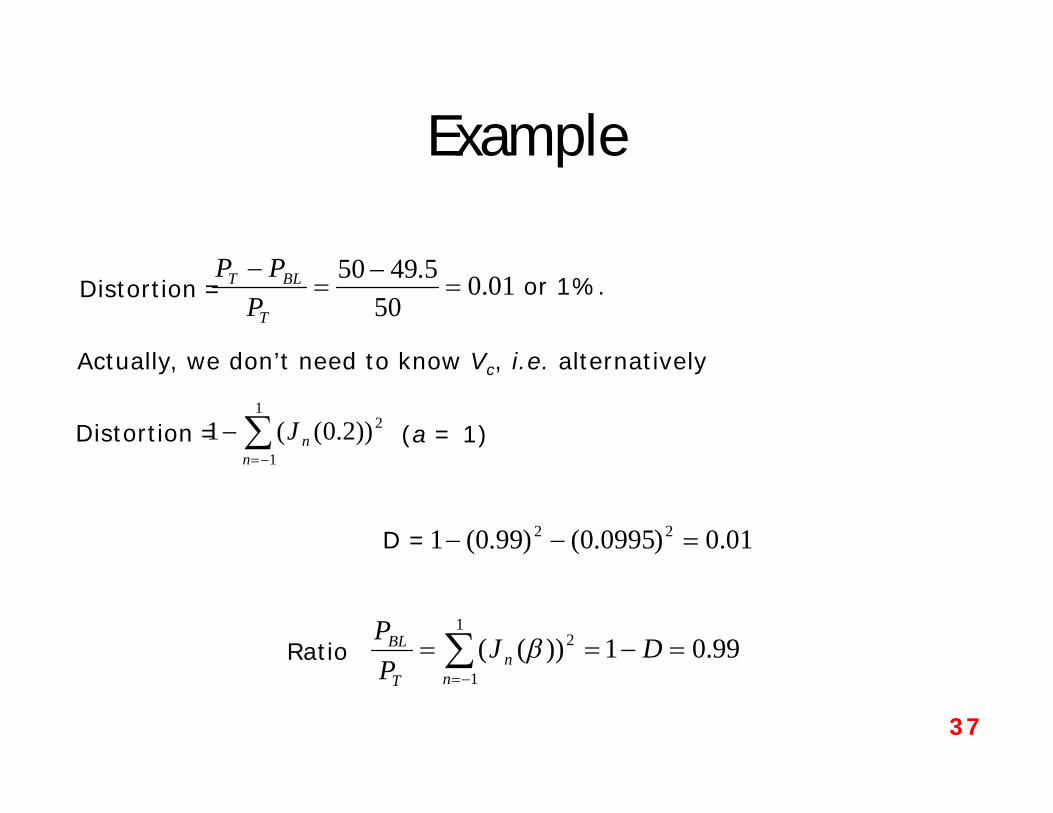
Example
Consider NBFM, with = 0.2. Let Vc = 10 volts. The total power in the infinite
2
2cV
spectrum = 50 Watts, i.e.
a
annJ 2))(( = 50 Watts.
From the table – the significant components are
n Jn(0.2) Amp = VcJn(0.2) Power =
2)( 2Amp
0 0.9900 9.90 49.005 1 0.0995 0.995 0.4950125
PBL = 49.5 Watts
i.e. the carrier + 2 sidebands contain 99.050
5.49 or 99% of the total power
36
Example
Distortion = 01.050
5.4950
T
BLT
PPP
or 1%.
Actually, we don’t need to know Vc, i.e. alternatively
Distortion =
1
1
2))2.0((1n
nJ (a = 1)
D = 01.0)0995.0()99.0(1 22
Ratio 99.01))((1
1
2
DJPP
nn
T
BL
37
FM Demodulation –General Principles.
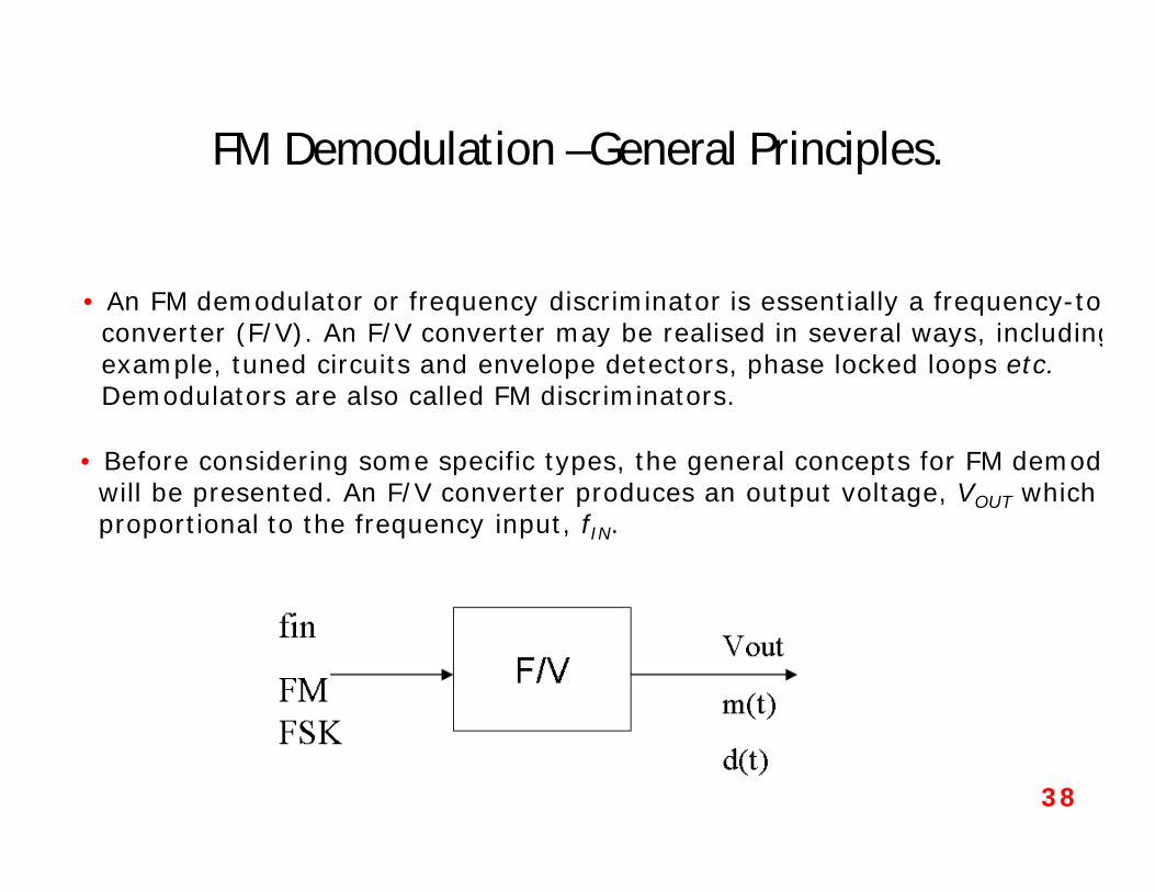
• An FM demodulator or frequency discriminator is essentially a frequency-to-converter (F/V). An F/V converter may be realised in several ways, including for example, tuned circuits and envelope detectors, phase locked loops etc.Demodulators are also called FM discriminators.
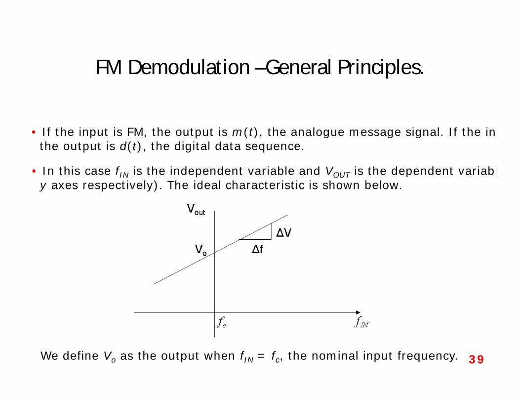
• Before considering some specific types, the general concepts for FM demodulation will be presented. An F/V converter produces an output voltage, VOUT which is proportional to the frequency input, fIN.
38
FM Demodulation –General Principles.
• If the input is FM, the output is m(t), the analogue message signal. If the input is FSK, the output is d(t), the digital data sequence.
• In this case fIN is the independent variable and VOUT is the dependent variable (y axes respectively). The ideal characteristic is shown below.
We define Vo as the output when fIN = fc, the nominal input frequency. 39

FM Demodulation –General Principles.
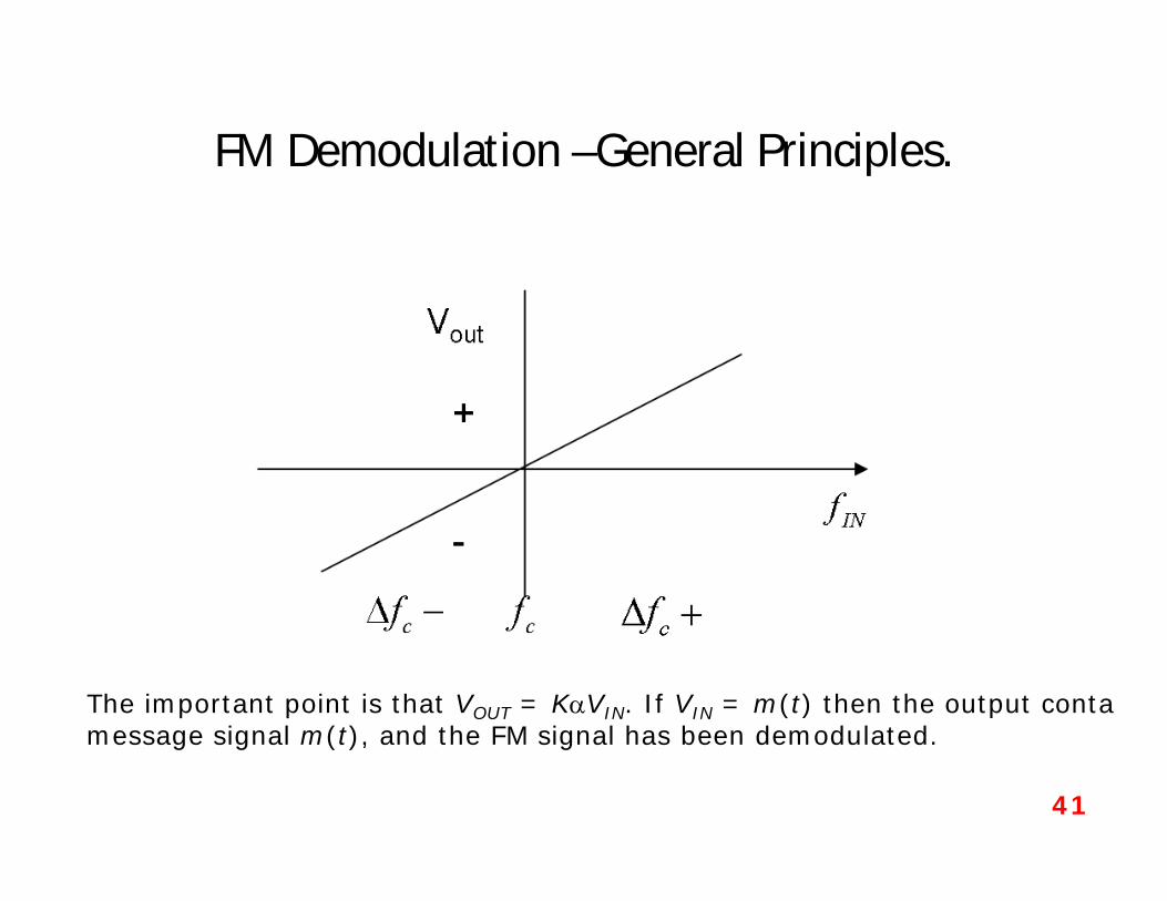
The gradient fV
is called the voltage conversion factor
i.e. Gradient = Voltage Conversion Factor, K volts per Hz.
Considering y = mx + c etc. then we may say VOUT = V0 + KfIN from the frequency modulator, and since V0 = VOUT when fIN = fc then we may write
INOUT VKVV 0
where V0 represents a DC offset in VOUT. This DC offset may be removed by level shifting or AC coupling, or the F/V may be designed with the characteristic shown next
40
FM Demodulation –General Principles.
The important point is that VOUT = KVIN. If VIN = m(t) then the output contains the message signal m(t), and the FM signal has been demodulated.
41

FM Demodulation –General Principles.
Often, but not always, a system designed so that 1
K , so that K = 1 and
VOUT = m(t). A complete system is illustrated.
42

FM Demodulation –General Principles.
43

Methods
Tuned Circuit – One method (used in the early days of FM) is to use the slope of a tuned circuit in conjunction with an envelope detector.
44
Methods
• The tuned circuit is tuned so the fc, the nominal input frequency, is on the slope, not at the centre of the tuned circuits. As the FM signal deviates about fc on the tuned circuit
slope, the amplitude of the output varies in proportion to the deviation from the FM signal is effectively converted to AM. This is then envelope detected by the diode etc to recover the message signal.
• Note: In the early days, most radio links were AM (DSBAM). When FM came along,with its advantages, the links could not be changed to FM quickly. Hence, NBFM was used (with a spectral bandwidth = 2fm, i.e. the same as DSBAM). The carrier frequency fc was chosen and the IF filters were tuned so that fc fell on the slope of thefilter response. Most FM links now are wideband with much better demodulators.
• A better method is to use 2 similar circuits, known as a Foster-Seeley Discriminator
45

Foster-Seeley Discriminator
This gives the composite characteristics shown. Diode D2 effectively inverts the tuned circuit response. This gives the characteristic ‘S’ type detector.
46

Phase Locked Loops PLL
• A PLL is a closed loop system which may be used for FM demodulation. A full analytical description is outside the scope of these notes. A brief description ispresented. A block diagram for a PLL is shown below.
• Note the similarity with a synchronous demodulator. The loop comprises a multiplier, a low pass filter and VCO (V/F converter as used in a frequency modulator).
47

Phase Locked Loops PLL
• The input fIN is applied to the multiplier and multiplied with the VCO frequency output fO, to produce = (fIN + fO) and = (fIN – fO).
• The low pass filter passes only (fIN – fO) to give VOUT which is proportional to (fIN – fO).
• If fIN fO but not equal, VOUT = VIN, fIN – fO is a low frequency (beat frequency) signal to the VCO.
• This signal, VIN, causes the VCO output frequency fO to vary and move towards fIN.
• When fIN = fO, VIN (fIN – fO) is approximately constant (DC) and fO is held constant, i.e locked to fIN.
• As fIN changes, due to deviation in FM, fO tracks or follows fIN. VOUT = VIN changes to drive fO to track fIN.
• VOUT is therefore proportional to the deviation and contains the message signal m(t).
48

UNIT-III
RADIO RECEIVERS
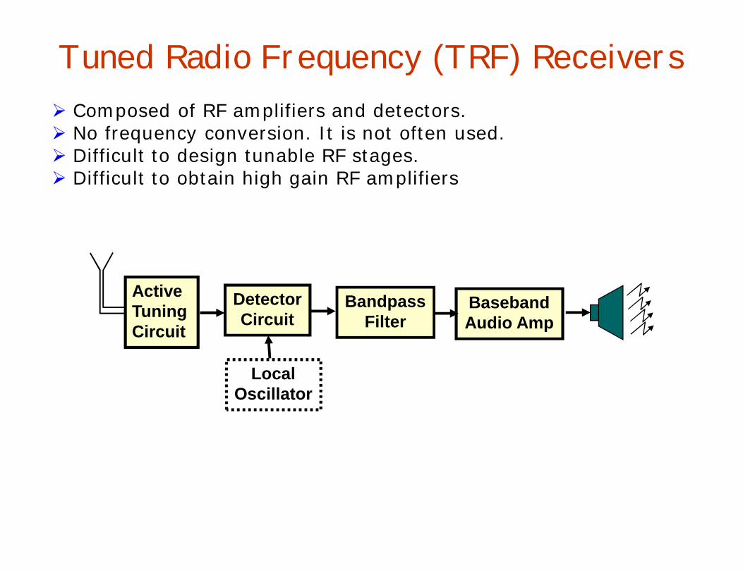
Tuned Radio Frequency (TRF) Receivers
ActiveTuningCircuit
DetectorCircuit
LocalOscillator
BandpassFilter
BasebandAudio Amp
Composed of RF amplifiers and detectors. No frequency conversion. It is not often used. Difficult to design tunable RF stages. Difficult to obtain high gain RF amplifiers

Heterodyning(Upconversion/Downconversion)
SubsequentProcessing(common)
AllIncomingFrequencies
FixedIntermediateFrequency
Heterodyning

Superheterodyne Receivers
Superheterodyne Receiver Diagram

Superheterodyne Receiver

Superheterodyne Receivers The RF and IF frequency responses H1(f) and H2(f) are important in providing the required reception characteristics.

Superheterodyne Receivers
fIF
fIF
RF Response
IF Response

Superheterodyne Receivers

Superheterodyne Receiver Frequencies
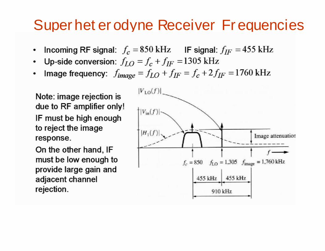
Superheterodyne Receiver Frequencies

Frequency Conversion Process

Image frequency not a problem.
Image Frequencies
Image frequency is also Image frequency is also receivedreceived

AM Radio Receiver

Superheterodyne Receiver Typical Signal Levels

Double-conversion block diagram.

Noise in Communication Noise in Communication SystemsSystems
115
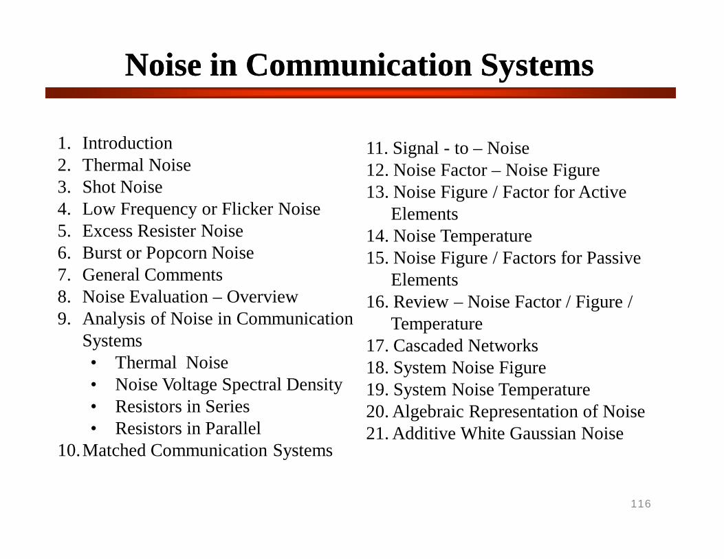
Noise in Communication SystemsNoise in Communication Systems
116
1. Introduction2. Thermal Noise3. Shot Noise4. Low Frequency or Flicker Noise5. Excess Resister Noise6. Burst or Popcorn Noise7. General Comments8. Noise Evaluation – Overview9. Analysis of Noise in Communication
Systems• Thermal Noise• Noise Voltage Spectral Density• Resistors in Series• Resistors in Parallel
10.Matched Communication Systems
11. Signal - to – Noise12. Noise Factor – Noise Figure13. Noise Figure / Factor for Active
Elements14. Noise Temperature15. Noise Figure / Factors for Passive
Elements16. Review – Noise Factor / Figure /
Temperature17. Cascaded Networks18. System Noise Figure19. System Noise Temperature20. Algebraic Representation of Noise21. Additive White Gaussian Noise

1. Introduction. Introduction
117
Noise is a general term which is used to describe an unwanted signal which affects a wanted signal. These unwanted signals arise from a variety of sources which may be considered in one of two main categories:-
•Interference, usually from a human source (man made)•Naturally occurring random noise
Interference
Interference arises for example, from other communication systems (cross talk), 50 Hz supplies (hum) and harmonics, switched mode power supplies, thyristor circuits, ignition (car spark plugs) motors … etc.

1. Introduction (Cont’d). Introduction (Cont’d)
118
Natural Noise
Naturally occurring external noise sources include atmosphere disturbance (e.g. electric storms, lighting, ionospheric effect etc), so called ‘Sky Noise’ or Cosmic noise which includes noise from galaxy, solar noise and ‘hot spot’ due to oxygen and water vapour resonance in the earth’s atmosphere.

2. Thermal Noise (Johnson Noise)2. Thermal Noise (Johnson Noise)
119
This type of noise is generated by all resistances (e.g. a resistor, semiconductor, the resistance of a resonant circuit, i.e. the real part of the impedance, cable etc).
Experimental results (by Johnson) and theoretical studies (by Nyquist) give the mean square noise voltage as
)(4 22_
voltTBRkV
Where k = Boltzmann’s constant = 1.38 x 10⁻²³ Joules per KT = absolute temperatureB = bandwidth noise measured in (Hz)R = resistance (ohms)

2. Thermal Noise (Johnson Noise) (Cont’d)2. Thermal Noise (Johnson Noise) (Cont’d)
120
The law relating noise power, N, to the temperature and bandwidth is
N = k TB wattsN = k TB watts
Thermal noise is often referred to as ‘white noise’ because it has a uniform ‘spectral density’.

3. Shot Noise3. Shot Noise
121
• Shot noise was originally used to describe noise due to random fluctuations in electron emission from cathodes in vacuum tubes (called shot noise by analogy with lead shot).• Shot noise also occurs in semiconductors due to the liberation of charge carriers.• For pn junctions the mean square shot noise current is
Whereis the direct current as the pn junction (amps)is the reverse saturation current (amps)is the electron charge = 1.6 x 10⁻¹⁹ coulombs
B is the effective noise bandwidth (Hz)
• Shot noise is found to have a uniform spectral density as for thermal noise
) 22 )(22 ampsBqIII eoDCn

4. Low Frequency or Flicker Noise4. Low Frequency or Flicker Noise
122
Active devices, integrated circuit, diodes, transistors etc also exhibits a low frequency noise, which is frequency dependent (i.e. non uniform) known as flicker noise or ‘one – over – f’ noise.
5. Excess Resistor Noise5. Excess Resistor NoiseThermal noise in resistors does not vary with frequency, as previously noted, by many resistors also generates as additional frequency dependent noise referred to as excess noise.
6. Burst Noise or Popcorn Noise6. Burst Noise or Popcorn NoiseSome semiconductors also produce burst or popcorn noise with a spectral density which is proportional to
21
f

7. General Comments7. General Comments
123
For frequencies below a few KHz (low frequency systems), flicker and popcorn noise are the most significant, but these may be ignored at higher frequencies where ‘white’ noise predominates.
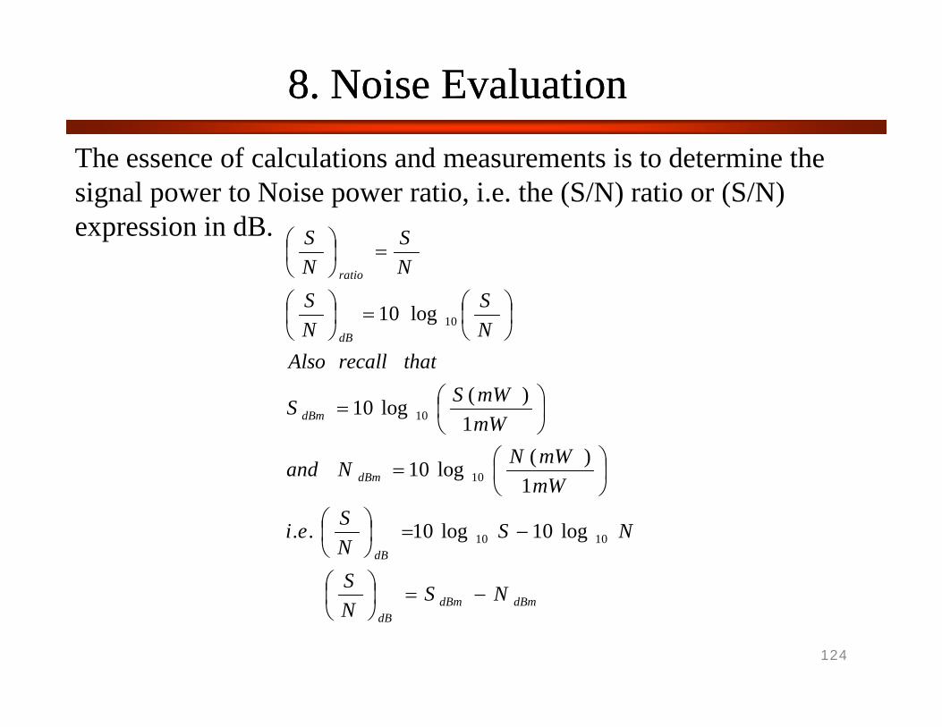
8. Noise Evaluation8. Noise Evaluation
124
The essence of calculations and measurements is to determine the signal power to Noise power ratio, i.e. the (S/N) ratio or (S/N) expression in dB.
dBmdBmdB
dB
dBm
dBm
dB
ratio
NSNS
NSNSei
mWmWNNand
mWmWSS
thatrecallAlsoNS
NS
NS
NS
1010
10
10
10
log10log10..
1)(log10
1)(log10
log10
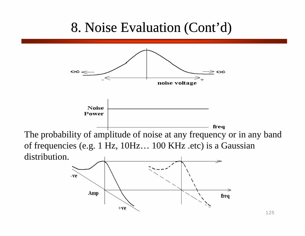
8. Noise Evaluation (Cont’d)8. Noise Evaluation (Cont’d)
125
The probability of amplitude of noise at any frequency or in any band of frequencies (e.g. 1 Hz, 10Hz… 100 KHz .etc) is a Gaussian distribution.
8. Noise Evaluation (Cont’d)8. Noise Evaluation (Cont’d)
126
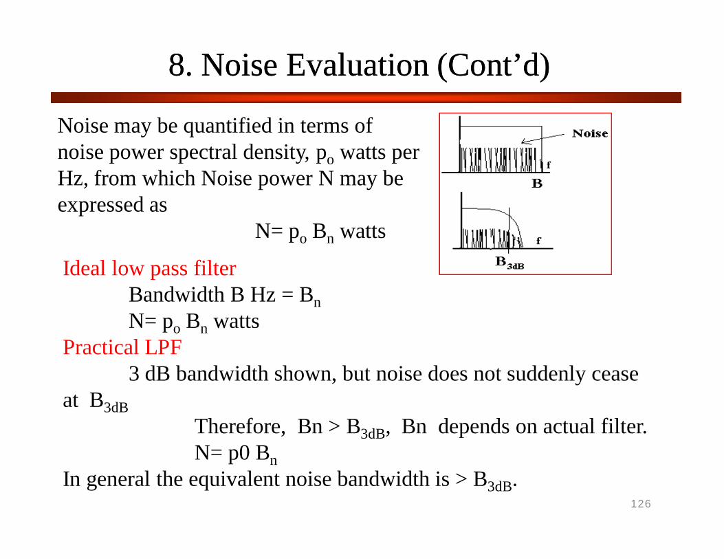
Noise may be quantified in terms of noise power spectral density, po watts per Hz, from which Noise power N may be expressed as
N= po Bn watts
Ideal low pass filterBandwidth B Hz = BnN= po Bn watts
Practical LPF3 dB bandwidth shown, but noise does not suddenly cease
at B3dBTherefore, Bn > B3dB, Bn depends on actual filter.N= p0 Bn
In general the equivalent noise bandwidth is > B3dB.

9. Analysis of Noise In Communication Systems9. Analysis of Noise In Communication Systems
127
Thermal Noise (Johnson noise)Thermal Noise (Johnson noise)This thermal noise may be represented by an equivalent circuit as shown below
)(4 2____
2 voltTBRkV
____2V nVkTBR 2
(mean square value , power)then VRMS =
i.e. Vn is the RMS noise voltage.
A) System BW = B Hz N= Constant B (watts) = KB
B) System BWN= Constant 2B (watts) = K2B
For A,KBS
NS
For B,BK
SNS
2

9. Analysis of Noise In Communication Systems (Cont’d)9. Analysis of Noise In Communication Systems (Cont’d)
128
22
___2
1
_______2
nnn VVV
11
____2
1 4 RBTkVn
22
____2
2 4 RBTkVn
)(4 2211
____2 RTRTBkVn
)(4 21
____2 RRBkTVn
Assume that R1 at temperature T1 and R2 at temperature T2, then
i.e. The resistor in series at same temperature behave as a single resistor
Resistors in SeriesResistors in Series

9. Analysis of Noise In Communication Systems (Cont’d)9. Analysis of Noise In Communication Systems (Cont’d)
129
Resistance in ParallelResistance in Parallel
21
211 RR
RVV no
21
122 RR
RVV no
22
___2
1
_______2
oon VVV
____
2nV )
21
2122
2111
222
21
4RRRRRTRRTR
RRkB
)221
221121_____
2 )(4RR
RTRTRRkBVn
21
21_____
2 4RR
RRkTBVn
10. 10. Matched Communication Systems Matched Communication Systems
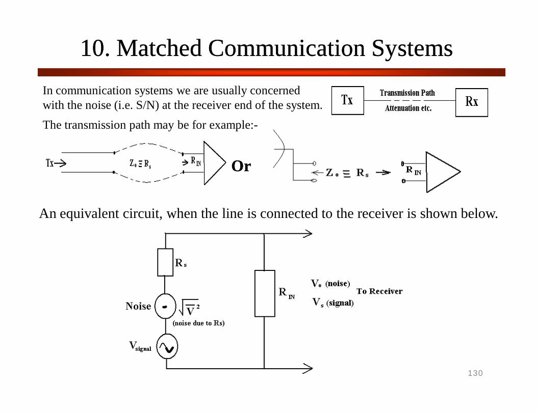
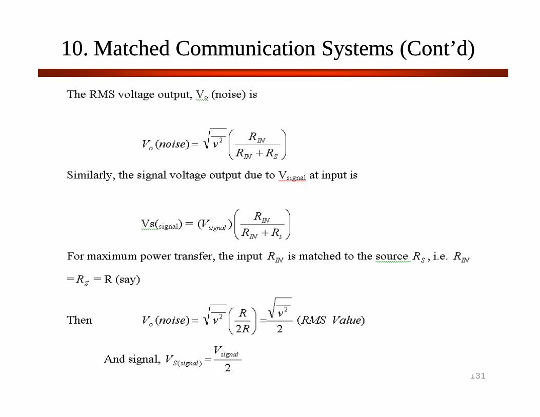
130
In communication systems we are usually concerned with the noise (i.e. S/N) at the receiver end of the system.The transmission path may be for example:-
OrOr
An equivalent circuit, when the line is connected to the receiver is shown below.
10. 10. Matched Communication Systems (Cont’d) Matched Communication Systems (Cont’d)
131
11. 11. Signal to NoiseSignal to Noise
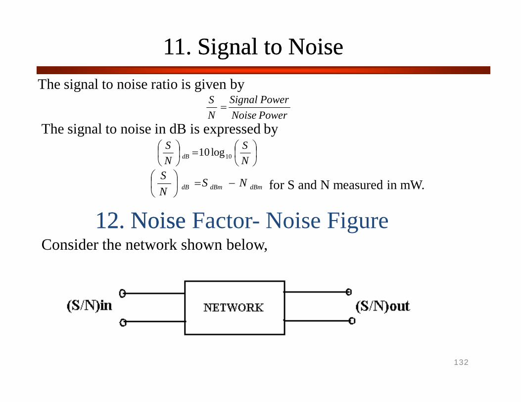
132
PowerNoisePowerSignal
NS
NS
NS
dB 10log10
The signal to noise ratio is given by
The signal to noise in dB is expressed by
dBmdBmdB NSNS
for S and N measured in mW.
12. 12. NoiseNoise Factor- Noise Figure Consider the network shown below,
133
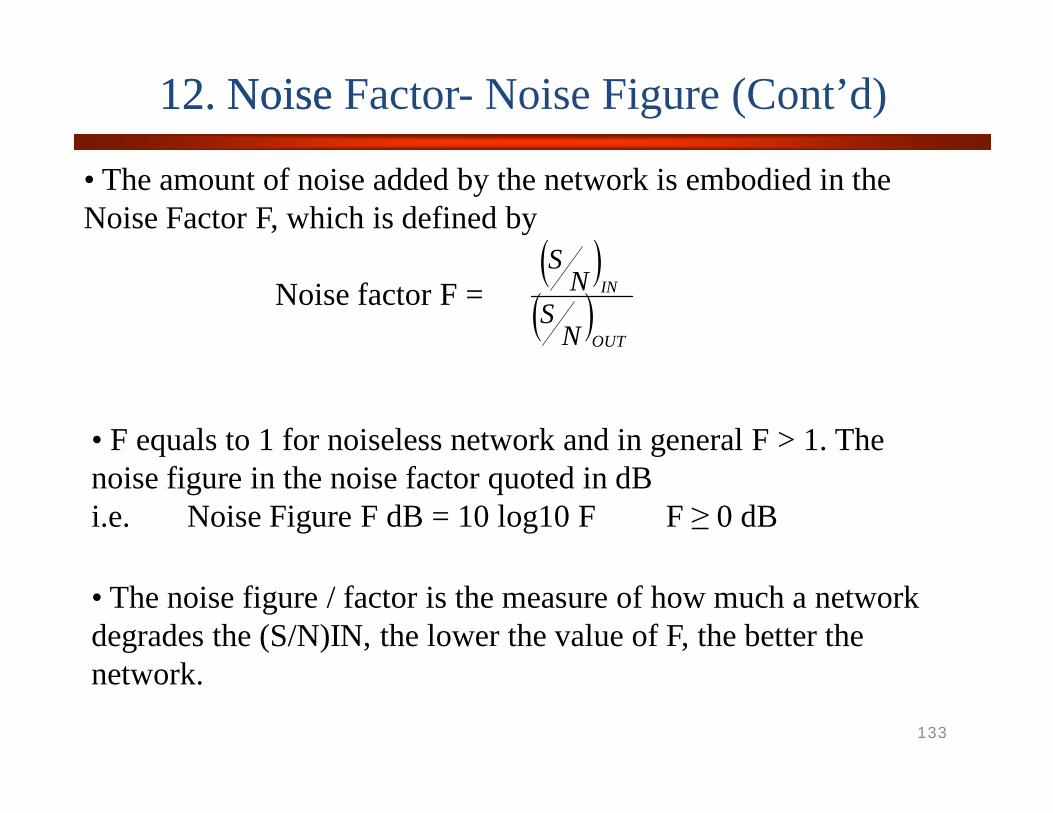
12. 12. NoiseNoise Factor- Noise Figure (Cont’d)
• The amount of noise added by the network is embodied in the Noise Factor F, which is defined by
Noise factor F = )
)OUT
IN
NS
NS
• F equals to 1 for noiseless network and in general F > 1. The noise figure in the noise factor quoted in dBi.e. Noise Figure F dB = 10 log10 F F ≥ 0 dB
• The noise figure / factor is the measure of how much a network degrades the (S/N)IN, the lower the value of F, the better the network.
13. 13. Noise Figure Noise Figure –– Noise Factor for Active ElementsNoise Factor for Active Elements
134
) )
OUT
IN
NS
NS
OUT
OUT
IN
IN
SN
NS
OUTS INSG
IN
OUT
IN
IN
SGN
NSF
IN
OUT
NGN
For active elements with power gain G>1, we have
F = = But
Therefore
Since in general F v> 1 , then OUTN is increased by noise due to the active element i.e.
Na represents ‘added’ noise measured at the output. This added noise may be referred to the input as extra noise, i.e. as equivalent diagram is
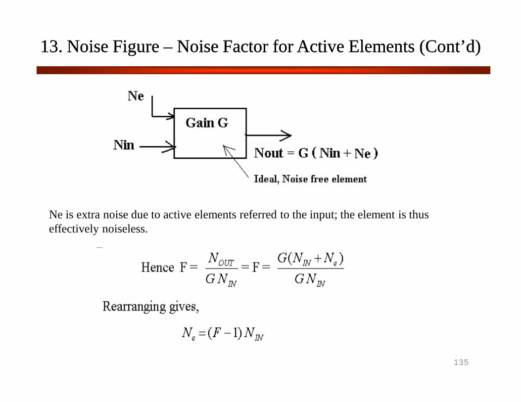
13. 13. Noise Figure Noise Figure –– Noise Factor for Active Elements (Cont’d)Noise Factor for Active Elements (Cont’d)
135
Ne is extra noise due to active elements referred to the input; the element is thus effectively noiseless.

14. 14. NoiseNoise Temperature
136

15. 15. Noise Figure Noise Figure –– Noise Factor for Passive ElementsNoise Factor for Passive Elements
137

16. Review of Noise Factor – Noise Figure –Temperature
138

17. 17. Cascaded NetworkCascaded Network
139
A receiver systems usually consists of a number of passive or active elements connected in series. A typical receiver block diagram is shown below, with example
In order to determine the (S/N) at the input, the overall receiver noise figure or noise temperature must be determined. In order to do this all the noise must be referred to the same point in the receiver, for example to A, the feeder input or B, the input to the first amplifier.
eT eNor is the noise referred to the input.
18. System 18. System NoiseNoise Figure
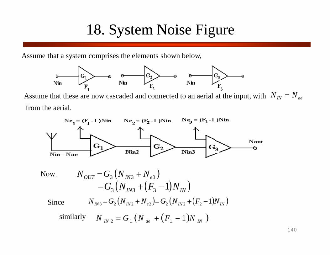
140
Assume that a system comprises the elements shown below,
Assume that these are now cascaded and connected to an aerial at the input, with aeIN NN
from the aerial.
Now , )333 eINOUT NNGN ) )ININ NFNG 1333
Since ) ) )ININeININ NFNGNNGN 12222223
similarly ) )INaeIN NFNGN 1112

18. System 18. System NoiseNoise Figure (Cont’d)
141
) ) ) INININaeOUT NFGNFGNFGNGGGN 111 332211123
The overall system Noise Factor is
ae
OUT
IN
OUTsys NGGG
NGNN
F321
) ) )ae
IN
ae
IN
ae
IN
NN
GGF
NN
GF
NN
F21
3
1
21
1111
) ) ) )121321
4
21
3
1
21 ..........
1...........111
n
nsys GGG
FGGG
FGG
FG
FFF
The equation is called FRIIS Formula.

19. System 19. System NoiseNoise Temperature
142

20. Algebraic Representation of 20. Algebraic Representation of NoiseNoise
143
Phasor Representation of Signal and NoiseThe general carrier signal VcCosWct may be represented as a phasor at any instant in time as shown below:
If we now consider a carrier with a noise voltage with “peak” value superimposed we may represents this as:
Both Vn and n are random variables, the above phasor diagram represents a snapshot
at some instant in time.
Chapter 5. Noise in CW Modulation System
144

Noise in CW ModulationSystem
•5.1 Introduction• - Receiver Noise (Channel Noise) :• additive, White, and Gaussian 으로 가정
•5.2 Receiver Model• 1. RX Model
•
2
2
Sw(f)
N 0
fRw()
N 0 ( )
•N0 = KTe where K = Boltzmann’s constant
•Te = equivalent noise Temp.
•Average noise power per unit bandwidth
- w(t): additive, white, and Gaussian, power spectraldensity N0
2
145

• - Band Pass Filter (Idealcase)
• w(t) n(t)•• - filtered noise as narrow-band
noise•
• n(t) = nI(t)cos(2pfCt) - nQ(t)sin(2pfCt)where nI(t) is inphase, nQ(t) is quadraturecomponent
• - filtered signal x(t)• x(t) = s(t) + n(t)•• - Average Noise Power = N0BT
•
BPF
receiver output
O
I
average power of the noise- (SNR)
average power of the filtered noise n(t)
average power of the demodulate d message signal
- (SNR) average power of the modulated signal s(t)
2B
N0
2B
SNI, SNQ
146

- DSB
- SSB
1 SM(f)
f
SS(f)
21
4
f f
SY(f)
1
4
4 2
C M CS M
Cm(t) P
- s(t) m(t)cos(2π fCt Θ) S (f) 1 S (f f ) S (f f )
m(t)cos(2π f t) 2 (P) P
N0
2
f f
SS(f)N0
2
2
22 00
1m(t) 1n (t)2 I
4W N0 2WN2W N0 WN
2 2C C
4 2 2 41 m(t)cos(2π f t) 1 mˆ
(t)sin(2π f t) 1 P P P
4 2 2
22
I Q
00
1 m(t) 1 n (t)cos(π Wt) 1 n (t) sin(π Wt)
2W N0 W N2W N0 W N
f
114
f
N0
2
f f
N0
2
147

• - s(t) by each system has the same average power• - noise w(t) has the same average power measured in the
message• BW =W
• 1) ChannelSNR
• 2)
•Noise in DSB-SCReceivers
•1. Model of DSB-SC Receivers
•
receiver input
C average power of the noise in the message BW at
average power of the modulated signal(SNR)
(SNR)C
(SNR)Figure of merit =
O
148

• 2. (SNR) O
- (SNR )
2(baseband)
2
2WN0
2 2
C,DSB
0
-W M
C ACP
- Average noise power 2W N0 WN
C2 A2 P- Average power of s(t) C
P ∫ W S (f) df
- s(t) CAC cos(2π fCt)m(t)whe re C : scaling factor Power spectral
density of m(t) : SM (f) W : message bandwidth
- Average signal power
2 2
211
2 2 21 1
C I
C Q CCC IIC CA m(t) n(t) CA m(t) n(t)
∴ y(t) 1 CA m(t) 1
n (t)
cos(4π f t) A n (t) sin(4π f t)
- x(t) s(t) n(t) CAC cos(2π fCt)m(t) nI(t)cos(2π fCt) nQ (t) sin(2π fCt)- v(t) x(t)cos(2π fCt)
149

(passband)4 2
4
(SNR)O
2WN0WN0 2
2 2 2 2
O
0 0
1
C ACP 4 C ACP
- Average noise power 1 (2W)N 1 WN
C2 A 2 P- Average signal power C
(SNR )C DSBSC
∴ Figureof merit
- ∴ (SNR )
Power(nI(t)) Power of bandpass filterednoisen(t) 2WN0
C,SSB
C C C
C2A2P(SNR)
4 2 4 2 4C2A2 P C2A2 P C2A2P
se in SSB Rece2ivers• Noi2
C4WN0
- Message power C C C
(half of DSB)- Average noise power WN0 ( message BW 안의 Noise) (baseband)
•m-(t)SanSdBm̂(Mt) aroedothuolgaontael,dE[mw(ta)]v e0⇒m(t)and m̂(t)are uncorrelated⇒ their power spectral densities are additive
m(t) and m̂(t)has the same power spectral density
π fCt)mˆ (t)
s(t) 1 CA cos(2π f t)m(t) 1 CA sin(2
150

2W
2Wn(t) nI(t)cos 2π(fC )t - nQ(t) sin 2π(fC )t
151

- Figure ofmerit
- (SNR)
4 2 4 2 4
16
4 2 2
- Combinedoutput
(SNR)C SSB
(SNR)O
4WN0
2 2
O,SSB
0
C
C I Q
1 same asDSB - SC
C ACP
- Average noise power 1 WN0 1 WN0 1 WN (passband)
- Average signal power 1 C2 A2P
y(t) 1 CA m(t) 1 n (t) cos(π Wt) 1 n (t) sin(π Wt)
•5.4 Noise in AM Receiver•
2WN0
N0
C a
- Filtered signal x(t) s(t) n(t)
[AC ACkam(t) nI(t)]cos(2π fCt) - nQ (t)sin(2π fCt)
A2 (1 k2P)Ca
(SNR)C,AM
- Average noise power WN0 ← (2W 2 )
- Average signal power A2 (1 k2P) 2
- AM signals(t) AC [1 kam(t)]cos(2π fCt)
152

• ex1) Single -Tone Modulation
(SNR)- Figure ofmerit
- (SNR)
a
2kaP
C AM
(SNR)O
2WN0
2 2ACkaPO,AM
122 2
C C a I Q
11k2P
Avg carrier power Avg noisepower
Assume AC [1 kam(t)] nI(t),nQ (t) y(t) AC ACkam(t) nI(t)
A k m(t) n (t)] n (t) [A y(t) envelop of x(t)
ka ≤ 1조건
(SNR)(SNR)
2A
a m2
a m21k2A2
C AM
O
2m
mm
if μ 1, F.O.M 1 (max)3
1 1 k2 A2 2 μ 2
μ 2
s(t) AC[1μ cos(2π fmt)]cos(2π fCt)
m(t) A cos(2π f t) → P
where μ ka Am
153
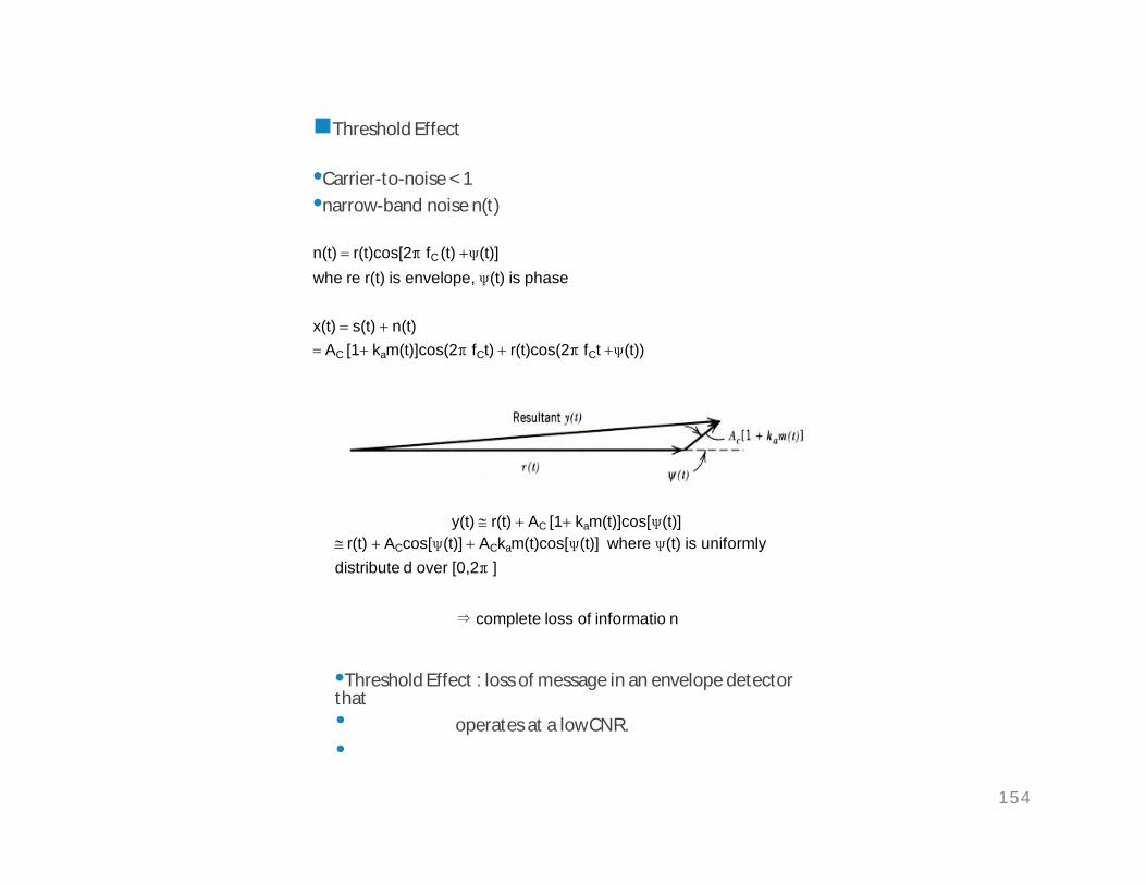
operates at a lowCNR.••
y(t) r(t) AC [1 kam(t)]cos[ψ(t)] r(t) ACcos[ψ(t)] ACkam(t)cos[ψ(t)] where ψ(t) is uniformly distribute d over [0,2π ]
⇒ complete loss of informatio n
•Threshold Effect : loss of message in an envelope detector that
Threshold Effect
•Carrier-to-noise < 1•narrow-band noise n(t)
n(t) r(t)cos[2π fC (t) ψ(t)]whe re r(t) is envelope, ψ(t) is phase
x(t) s(t) n(t) AC [1 kam(t)]cos(2π fCt) r(t)cos(2π fCt ψ(t))
154

•Noise in FM Receivers
• w(t) : zero mean white Gaussian noise with psd = No/2• s(t) : carrier =fc, BW = BT 즉 (fC BT/2)
• - BPF : [fC - BT/2 ~ fC + BT/2]• - Amplitude limiter : remove amplitude
variations• by clipping andBPF• -
Discriminator slope network or differentiator : varies linearly withfrequency
envelope detector• - Baseband LPF:
• - FM signal
• - Filtered noisen(t)
t
s(t) AC cos[2π fCt φ(t)]φ(t) 2π kf∫ 0 m(t)dt
s(t) AC cos[2π fCt 2π kf∫ t m(t)dt]0
r(t)where
nI(t) 1nQ(t)
(n (t))2 (n (t))2I Q
ψ(t) tan
n(t) nI(t)cos(2π fCt) nQ (t) sin(2π fCt) r(t)cos[2π fCt ψ(t)]
155
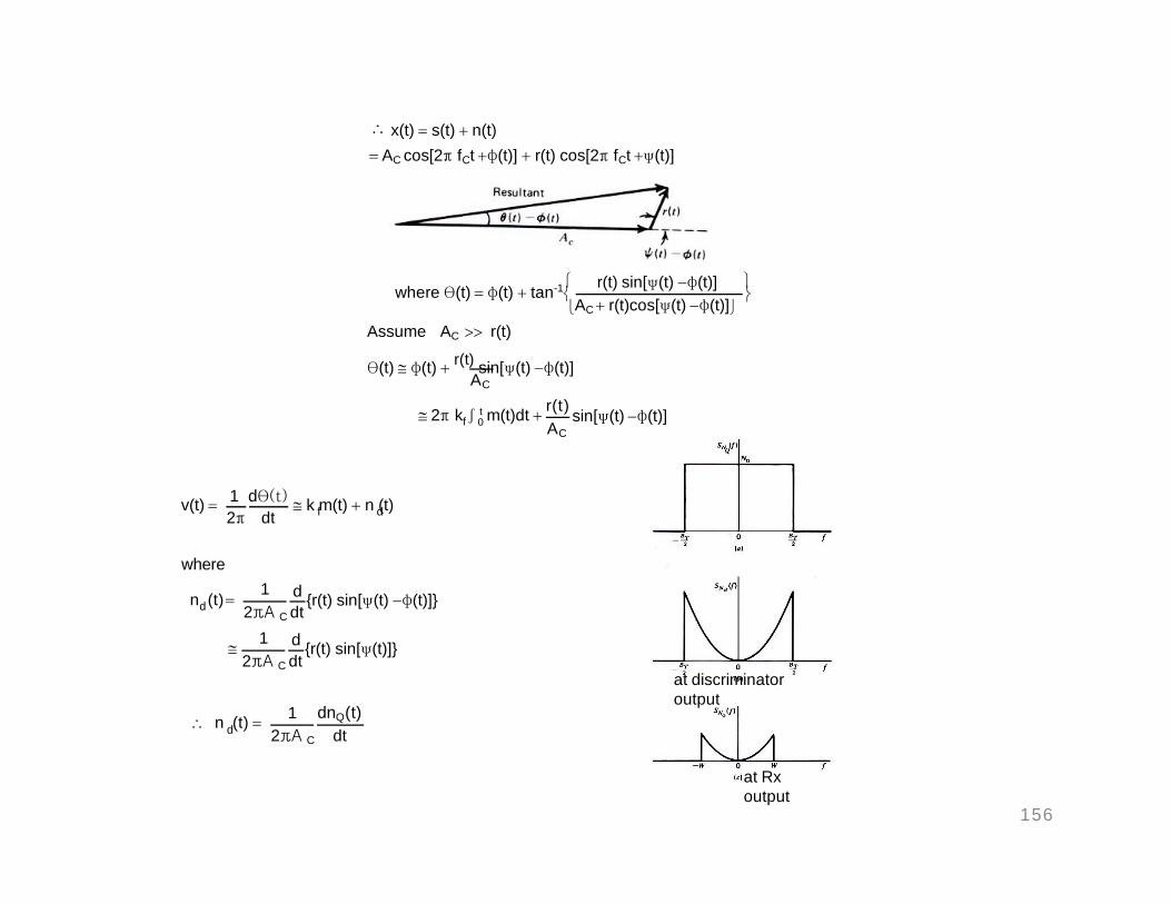
r(t)AC
tf 0
AC
sin[ψ(t) φ(t)] 2π k ∫ m(t)dt
Assume AC r(t)
θ(t) φ(t) r(t) sin[ψ(t) φ(t)]
AC r(t)cos[ψ(t) φ(t)] r(t) sin[ψ(t) φ(t)]where θ(t) φ(t) tan-1
∴ x(t) s(t) n(t) AC cos[2π fCt φ(t)] r(t) cos[2π fCt ψ(t)]
1
1where
1 dnQ(t)2πA C dtd
2πA C dt
2πA C dtd
f d
n (t)
n (t)
d {r(t) sin[ψ(t)]}
d {r(t) sin[ψ(t) φ(t)]}
v(t) 1 dθ(t) k m(t) n (t)2π dt
at discriminatoroutput
at Rxoutput
156

• Pre-emphasis and de-emphasis in FM
• P.S.D. of noise at FM Rx output
• P.S.D. of typical message signal
signal
noise
1
A2C
20
Nd
P.S.D of noise nd(t) at the discriminator output
0
N fS (f)
, - W f W
f T
2otherwise
de
B
Hpe (f )H (f )
157