understanding anadigm configurable analog modules (cams)
TRANSCRIPT

Understanding AnadigmUnderstanding Anadigm®®
Configurable Analog Modules (CAMs)Configurable Analog Modules (CAMs)

Anadigmvortex Technical Training PR021100-0024 November 2002 page 2
AgendaAgenda
What is a CAM?Configuring and Placing CAMsOther ConsiderationsCAMs Available in the Anadigm Standard Library

Anadigmvortex Technical Training PR021100-0024 November 2002 page 3
What is a Configurable Analog Module What is a Configurable Analog Module (CAM)?(CAM)?
Circuit building blocks abstracted to a functional level that can be manipulated in AnadigmDesigner®2
A complex circuit can be implemented in a “chip” simply by selecting, configuring, placing and wiring CAMs
Improved speed and ease of circuit design

Anadigmvortex Technical Training PR021100-0024 November 2002 page 4
AnadigmDesigner2AnadigmDesigner2®® CAMsCAMs
Very dynamic, powerful yet easy to use❍ Multiple circuit topologies – CAM knows how to
make what you ask for❍ Dynamic user interface – options and limits can
changeAllows user to push the limits of the CAMConstrains the user to legal configurations
Expanded CAM documentation explains the features

Anadigmvortex Technical Training PR021100-0024 November 2002 page 5
Selecting a CAMSelecting a CAM
•Library- ANx20 Standard
•Documentation
•Description- Biquadratic Filter
•Name- FilterBiquad

Configuring the CAM - Clocks
• Set the clock(s)
• CAMs with multiple clocks contain instructions about their relation
– Spinners– associate CAM clocks (CLOCKA)– with chip clocks (Clock 0) and show the frequency of that chip clock
– Chip clock frequencies are set in the “Chip Settings” dialog box
• All CAMs in a signal path should use the same chip clock for the analog clock (CAM CLOCKA)
• Some CAM parameters are clock dependent (filter corner frequency)– These CAMs should be reconfigured if the clock frequencies are
changed

Configuring the CAM - Options
• CAM Options– Option settings control circuit configuration. This is reflected in
the symbol. Options and parameters may also change– Options may be gray due to incompatible combinations or
unavailable resources

Configuring the CAM - Parameters
• Parameter Names– May include units
• Parameter Limits– Values will be restricted
• Desired Value– Entered by the user
• Realized Value– What was possible for this
combination of desired values

Anadigmvortex Technical Training PR021100-0024 November 2002 page 9
Parameters - Quantization and Error
• Realized values show the implementation of the parameter based on ratios of programmable capacitor banks which are quantized
02575.02336
=capsunitcapsunit
• Actual measured values can have error in addition to the quantization of the realized value
errorGainGain
Measured
ealizedR
%6.00259.0
02575.0
⇒=
=

Anadigmvortex Technical Training PR021100-0024 November 2002 page 10
Parameters - Interrelation
• Realized values are based on the combination of capacitor ratios. Changing one desired value can change multiple realized values.
02564.0391
=capsunitcapsunit0.6
39234
=capsunitcapsunit
• Limits are dynamic. Changing desired values can also change the limits.– If Gain 1 = 6.0Gain 2 cannot be less than 0.0235– If Gain 2 = .0257Gain 1 cannot be greater than 6.55

Configuring the CAM Configuring the CAM -- LUTLUT
• Parameter entry to set output voltages– Limits– Input voltage range that
will trigger this output– Desired value– Realized value

Configuring the CAM - Finishing
Read any notes for help with configuration
• Documentation– Online help about this CAM
• Cancel– Discard all changes
• OK– Accept all changes

Anadigmvortex Technical Training PR021100-0024 November 2002 page 13
Online CAM DocumentationOnline CAM Documentation• Anadigm approved CAMs contain
information about CAM construction and proper usage– Details about each CAM option– Details about each CAM parameter– Design Equations– Circuit Diagrams– Switch Phasing– Output Characteristics
• Some include additional design notes with information about special features of that CAM

Anadigmvortex Technical Training PR021100-0024 November 2002 page 14
Placing and Wiring CAMsPlacing and Wiring CAMs
Place the CAM within the chip bordersGreen warning marker indicates the CAM cannot be dropped on top of somethingRed warning marker indicates that available resources are not sufficient to implement the CAM
Draw wires between the CAM contactsOnly legal connections will be allowed
Chips can be connected for simulation

Anadigmvortex Technical Training PR021100-0024 November 2002 page 15
Other Considerations Other Considerations –– Clock PhasesClock Phases
Always see the CAM documentation for details on input/output characteristics
φ1 φ1 φ1φ2φ2 φ2
Each clock has two non-overlapping phasesPhase symbol on a CAM input shows an input that samples only on that phase– ∆φ indicates that the sampling
phase changes during operationPhase symbol on a CAM output shows the output should be sampled on that phaseWarning: a phased output can be safely connected only to a similarly phased input

Anadigmvortex Technical Training PR021100-0024 November 2002 page 16
Other Considerations Other Considerations –– Clock DelayClock DelayCAMs may have signal delay due to the timing of clocked switches. This is not the same as filter phase delay.Clock delay can often be neglected if the clock frequency is adequately higher than the signal frequency
Example – 10 kHz signal CAMhas half clock cycle delay– With 50 kHz clock36 degree delay (possibly significant)– With 1 MHz clock1.8 degree delay (probably negligible)
Clock delay is not shown by symbol aloneAlways see the CAM documentation for details on input/output characteristics

Anadigmvortex Technical Training PR021100-0024 November 2002 page 17
CAM FilesCAM Files
.cam File• Primary CAM file
• ASCII based
• Read directly by AnadigmDesigner2
• Strictly formatted, keyword driven with very little error checkingName, Version, User InterfaceControl, Circuit Definition, Parameter Calculation, Symbol, Simulation equations, CCODE, etc.
.chm File• CAM Documentation or
Help file
• Compiled HTML
• Referenced and displayed by AnadigmDesigner™
Anadigmvortex Technical Training PR021100-0024 November 2002 page 18
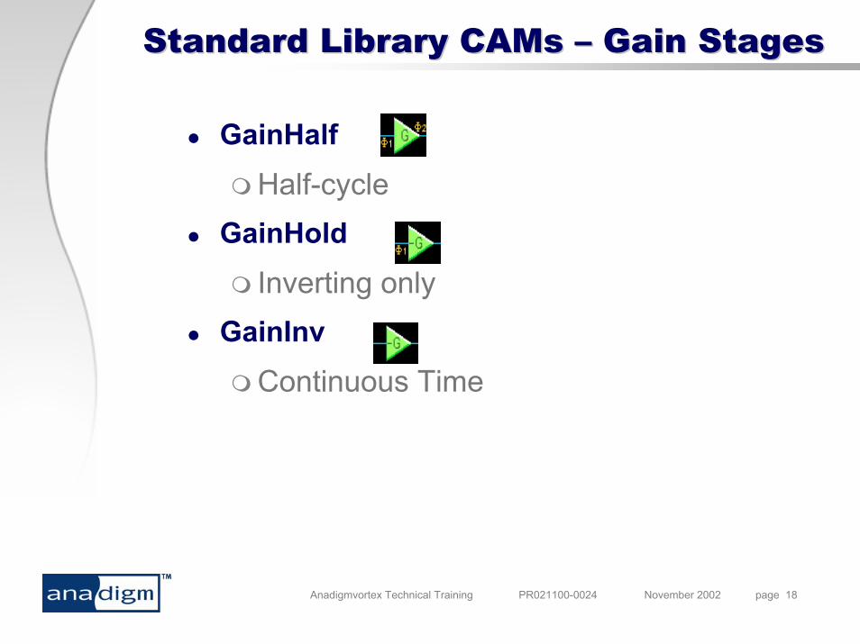
Standard Library CAMs Standard Library CAMs –– Gain StagesGain Stages
GainHalfHalf-cycle
GainHoldInverting only
GainInvContinuous Time

Anadigmvortex Technical Training PR021100-0024 November 2002 page 19
Standard Library CAMs Standard Library CAMs –– RectifiersRectifiers
RectifierFilter
Full Wave/Half Wave
Inverting/non-invertingRectifierHalf
Full Wave/Half Wave
Inverting/non-invertingRectifierHold
Half Wave Inverting only

Anadigmvortex Technical Training PR021100-0024 November 2002 page 20
Standard Library CAMs Standard Library CAMs –– SummingSumming
SumInvUp to three inputs
SumDiff (SumHalf)Up to four inputsAdd or subtract since input branches can be inverting or non-inverting

Anadigmvortex Technical Training PR021100-0024 November 2002 page 21
Standard Library CAMs Standard Library CAMs –– FiltersFilters
FilterBilinear – One poleLow Pass/High Pass/All Pass
FilterBiquad – Two polesLow Pass/High Pass/Band Pass/Band StopAutomatically chooses from multiple circuit topologies
Some other CAMs use a low pass bilinear filter as part of another function (RectifierFilter)

Anadigmvortex Technical Training PR021100-0024 November 2002 page 22
Standard Library CAMs Standard Library CAMs –– MathMath
DifferentiatorOutput voltage slews – see documentation
IntegratorOptional reset

Anadigmvortex Technical Training PR021100-0024 November 2002 page 23
Standard Library CAMs Standard Library CAMs –– MultiplierMultiplier
MultiplierUses SAR (Input Y is quantized)Subject to internal reference voltage errorOptional sample and hold on input X to equalize sampling time of two inputs (uses chip resources)

Anadigmvortex Technical Training PR021100-0024 November 2002 page 24
Standard Library CAMs Standard Library CAMs –– LUTLUT
PeriodicWaveHalf-cycle/Output HoldUses LUT to generate a user-defined periodic sequence of output voltagesDocumentation has help with loading the LUT
TransferFunctionHalf-cycle/Output HoldUses the SAR and LUT to perform A/D conversion on the input and generate the appropriate user-defined output voltage

Anadigmvortex Technical Training PR021100-0024 November 2002 page 25
Standard Library CAMs Standard Library CAMs -- OtherOther
Comparator
Single/Dual Input
Variable Reference
Hold – Sample and hold
OscillatorSine
Subject to internal reference voltage error
Voltage (+/- 3 VDC)
Subject to internal reference voltage error