ultrafast rectifier, 2 x 10 a fred pt - 4donline.ihs.com filemur.. series are the state of the art...
TRANSCRIPT

VS-MURB2020CTHM3, VS-MURB2020CT-1HM3www.vishay.com Vishay Semiconductors
Revision: 16-Jun-15 1 Document Number: 94807For technical questions within your region: [email protected], [email protected], [email protected]
THIS DOCUMENT IS SUBJECT TO CHANGE WITHOUT NOTICE. THE PRODUCTS DESCRIBED HEREIN AND THIS DOCUMENTARE SUBJECT TO SPECIFIC DISCLAIMERS, SET FORTH AT www.vishay.com/doc?91000
Ultrafast Rectifier, 2 x 10 A FRED Pt®
FEATURES• Ultrafast recovery time• Low forward voltage drop• Low leakage current• 175 °C operating junction temperature• Meets MSL level 1, per J-STD-020, LF maximum
peak of 260 °C• AEC-Q101 qualified
• Meets JESD 201 class 1 whisker test
• Material categorization: for definitions of compliance please see www.vishay.com/doc?99912
DESCRIPTION / APPLICATIONSMUR.. series are the state of the art ultrafast recovery rectifiers specifically designed with optimized performance of forward voltage drop and ultrafast recovery time.The planar structure and the platinum doped life time control, guarantee the best overall performance, ruggedness and reliability characteristics.These devices are intended for use in the output rectification stage of SMPS, UPS, DC/DC converters as well as freewheeling diode in low voltage inverters and chopper motor drives.Their extremely optimized stored charge and low recovery current minimize the switching losses and reduce over dissipation in the switching element and snubbers.
PRODUCT SUMMARYPackage TO-263AB (D2PAK), TO-262AA
IF(AV) 2 x 10 A
VR 200 V
VF at IF 0.85
trr typ. 19 ns
TJ max. 175 °C
Diode variation Common cathode
VS-MURB2020CTHM3
D2PAK
VS-MURB2020CT-1HM3
TO-262
Anode
Basecommoncathode
2Anode
1 3
2
Commoncathode
1 2Anode
Basecommoncathode
2Anode
1 3
2
Commoncathode
21
ABSOLUTE MAXIMUM RATINGSPARAMETER SYMBOL TEST CONDITIONS MAX. UNITS
Peak repetitive reverse voltage VRRM 200 V
Average rectified forward currentper leg
IF(AV)10
Atotal device Rated VR, TC = 145 °C 20
Non-repetitive peak surge current per leg IFSM 100
Peak repetitive forward current per leg IFM Rated VR, square wave, 20 kHz, TC = 145 °C 20
Operating junction and storage temperatures TJ, TStg -65 to +175 °C
ELECTRICAL SPECIFICATIONS (TJ = 25 °C unless otherwise specified)PARAMETER SYMBOL TEST CONDITIONS MIN. TYP. MAX. UNITS
Breakdown voltage,blocking voltage
VBR,VR
IR = 100 μA 200 - -
V
Forward voltage VF
IF = 8 A, TJ = 125 °C - - 0.85
IF = 16 A - - 1.15
IF = 16 A, TJ = 125 °C - - 1.05
Reverse leakage current IRVR = VR rated - - 15
μATJ = 150 °C, VR = VR rated - - 250
Junction capacitance CT VR = 200 V - 55 - pF
Series inductance LS Measured lead to lead 5 mm from package body - 8.0 - nH
VS-MURB2020CTHM3, VS-MURB2020CT-1HM3www.vishay.com Vishay Semiconductors
Revision: 16-Jun-15 2 Document Number: 94807For technical questions within your region: [email protected], [email protected], [email protected]
THIS DOCUMENT IS SUBJECT TO CHANGE WITHOUT NOTICE. THE PRODUCTS DESCRIBED HEREIN AND THIS DOCUMENTARE SUBJECT TO SPECIFIC DISCLAIMERS, SET FORTH AT www.vishay.com/doc?91000
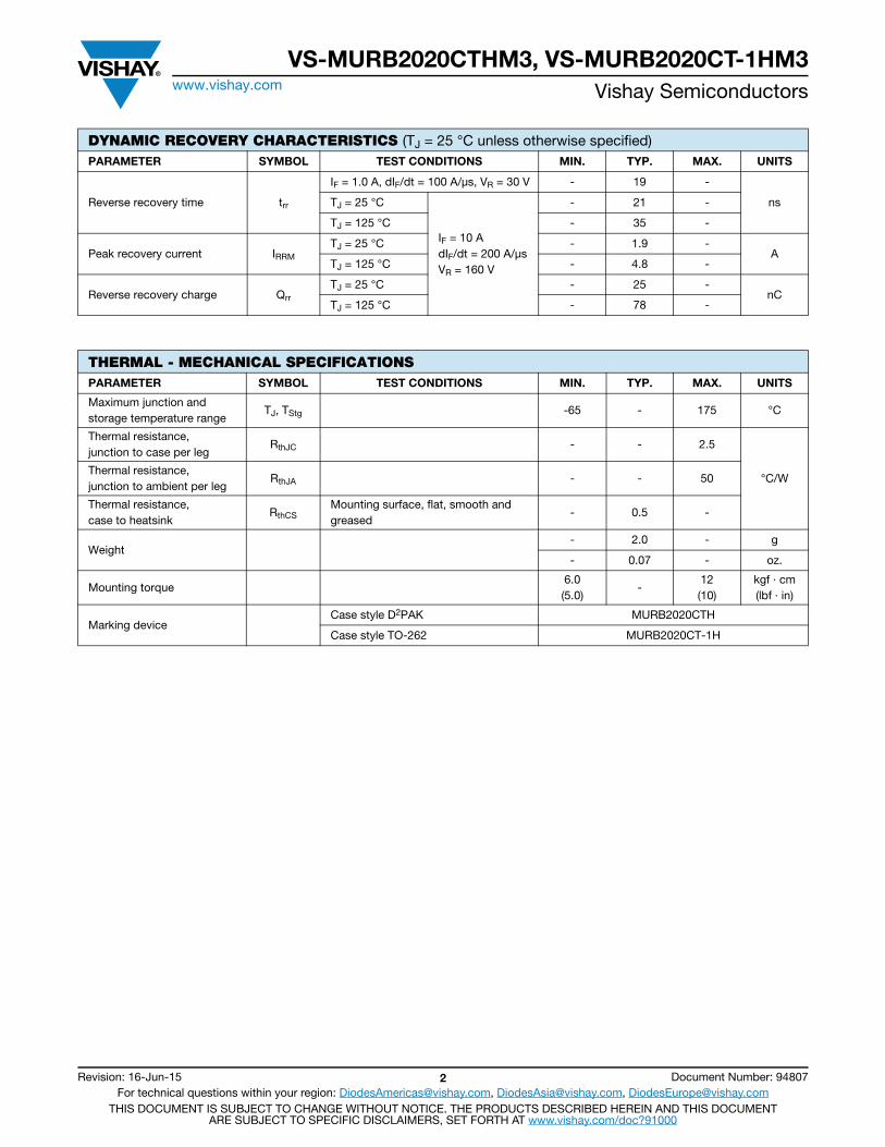
DYNAMIC RECOVERY CHARACTERISTICS (TJ = 25 °C unless otherwise specified)PARAMETER SYMBOL TEST CONDITIONS MIN. TYP. MAX. UNITS
Reverse recovery time trr
IF = 1.0 A, dIF/dt = 100 A/μs, VR = 30 V - 19 -
nsTJ = 25 °C
IF = 10 AdIF/dt = 200 A/μsVR = 160 V
- 21 -
TJ = 125 °C - 35 -
Peak recovery current IRRMTJ = 25 °C - 1.9 -
ATJ = 125 °C - 4.8 -
Reverse recovery charge QrrTJ = 25 °C - 25 -
nCTJ = 125 °C - 78 -
THERMAL - MECHANICAL SPECIFICATIONSPARAMETER SYMBOL TEST CONDITIONS MIN. TYP. MAX. UNITS
Maximum junction and storage temperature range
TJ, TStg -65 - 175 °C
Thermal resistance,junction to case per leg
RthJC - - 2.5
°C/WThermal resistance,junction to ambient per leg
RthJA - - 50
Thermal resistance,case to heatsink
RthCSMounting surface, flat, smooth and greased
- 0.5 -
Weight- 2.0 - g
- 0.07 - oz.
Mounting torque6.0(5.0)
-12(10)
kgf · cm(lbf · in)
Marking deviceCase style D2PAK MURB2020CTH
Case style TO-262 MURB2020CT-1H
VS-MURB2020CTHM3, VS-MURB2020CT-1HM3www.vishay.com Vishay Semiconductors
Revision: 16-Jun-15 3 Document Number: 94807For technical questions within your region: [email protected], [email protected], [email protected]
THIS DOCUMENT IS SUBJECT TO CHANGE WITHOUT NOTICE. THE PRODUCTS DESCRIBED HEREIN AND THIS DOCUMENTARE SUBJECT TO SPECIFIC DISCLAIMERS, SET FORTH AT www.vishay.com/doc?91000
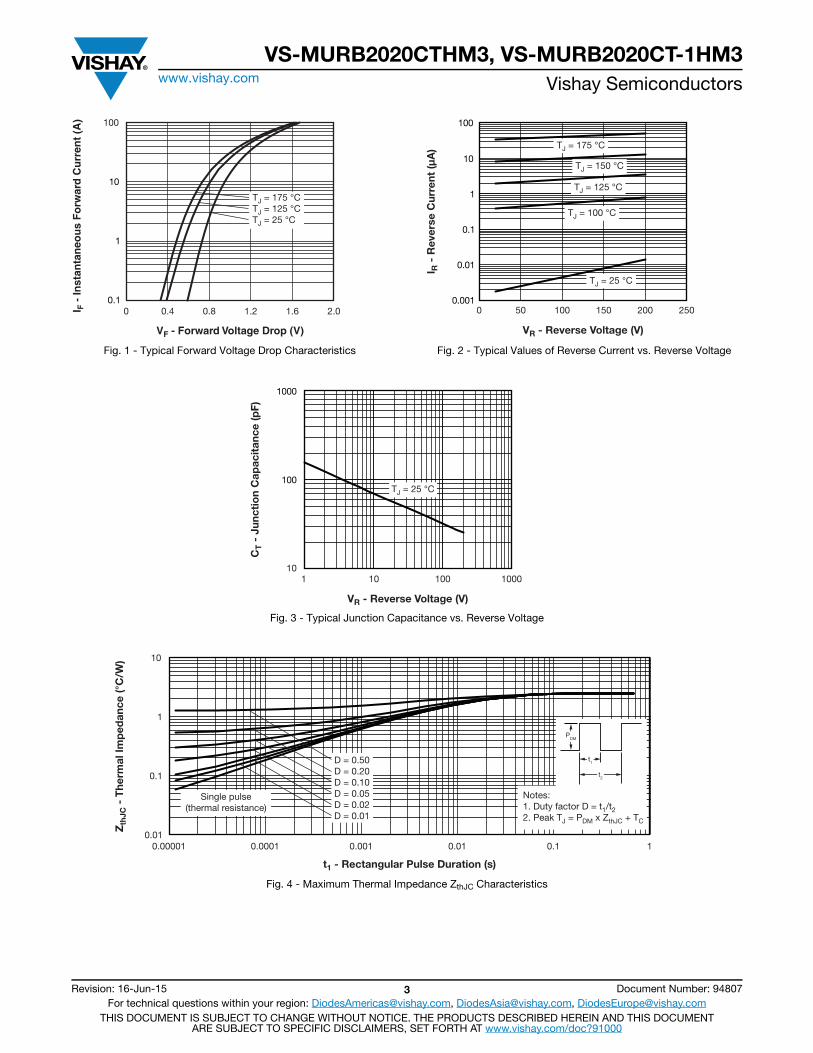
Fig. 1 - Typical Forward Voltage Drop Characteristics Fig. 2 - Typical Values of Reverse Current vs. Reverse Voltage
Fig. 3 - Typical Junction Capacitance vs. Reverse Voltage
Fig. 4 - Maximum Thermal Impedance ZthJC Characteristics
1
10
0 2.00.4 1.2
VF - Forward Voltage Drop (V)
I F -
Inst
anta
neo
us
Fo
rwar
d C
urr
ent
(A) 100
1.60.1
0.8
TJ = 175 °CTJ = 125 °CTJ = 25 °C
0.01
0.1
1
10
100
0 100 150
VR - Reverse Voltage (V)
I R -
Rev
erse
Cur
rent
(μA
)
200 250500.001
TJ = 125 °C
TJ = 175 °C
TJ = 150 °C
TJ = 100 °C
TJ = 25 °C
100
1000
1 10 100 100010
VR - Reverse Voltage (V)
CT -
Jun
ctio
n C
apac
itan
ce (p
F)
TJ = 25 °C
0.01
0.1
10
0.00001 0.0001 0.001 0.01 0.1 1
t1 - Rectangular Pulse Duration (s)
Zth
JC -
The
rmal
Imp
edan
ce (°
C/W
)
1
Single pulse(thermal resistance)
D = 0.50D = 0.20D = 0.10D = 0.05D = 0.02D = 0.01
PDM
t2
t1
Notes:1. Duty factor D = t1/t22. Peak TJ = PDM x ZthJC + TC

VS-MURB2020CTHM3, VS-MURB2020CT-1HM3www.vishay.com Vishay Semiconductors
Revision: 16-Jun-15 4 Document Number: 94807For technical questions within your region: [email protected], [email protected], [email protected]
THIS DOCUMENT IS SUBJECT TO CHANGE WITHOUT NOTICE. THE PRODUCTS DESCRIBED HEREIN AND THIS DOCUMENTARE SUBJECT TO SPECIFIC DISCLAIMERS, SET FORTH AT www.vishay.com/doc?91000
Fig. 5 - Maximum Allowable Case Temperature vs. Average Forward Current
Fig. 6 - Forward Power Loss Characteristics
Fig. 7 - Typical Reverse Recovery Time vs. dIF/dt
Fig. 8 - Typical Stored Charge vs. dIF/dt
Note(1) Formula used: TC = TJ - (Pd + PdREV) x RthJC;
Pd = Forward power loss = IF(AV) x VFM at (IF(AV)/D) (see fig. 6);PdREV = Inverse power loss = VR1 x IR (1 - D); IR at VR1 = Rated VR
0 3
Allo
wab
le C
ase
Tem
per
atu
re (
°C)
IF(AV) - Average Forward Current (A)
160
170
180
See note (1)
150
DC
140
1306 9
Square wave (D = 0.50)Rated VR applied
12 15
0 6
Ave
rag
e P
ow
er L
oss
(W)
IF(AV) - Average Forward Current (A)
0
D = 0.01D = 0.02D = 0.05D = 0.10D = 0.20D = 0.50DC
3 9
3
6
15
9
12
12 15
RMS limit
100 1000
t rr (
ns)
dIF/dt (A/μs)
20
40
VR = 160 VTJ = 125 °CTJ = 25 °C
30
50
10 IF = 20 AIF = 10 AIF = 5 A
0
100 1000
Qrr
(nC
)
dIF/dt (A/μs)
50
250
150
VR = 160 VTJ = 125 °CTJ = 25 °C
100
200
0
IF = 20 AIF = 10 AIF = 5 A
VS-MURB2020CTHM3, VS-MURB2020CT-1HM3www.vishay.com Vishay Semiconductors
Revision: 16-Jun-15 5 Document Number: 94807For technical questions within your region: [email protected], [email protected], [email protected]
THIS DOCUMENT IS SUBJECT TO CHANGE WITHOUT NOTICE. THE PRODUCTS DESCRIBED HEREIN AND THIS DOCUMENTARE SUBJECT TO SPECIFIC DISCLAIMERS, SET FORTH AT www.vishay.com/doc?91000
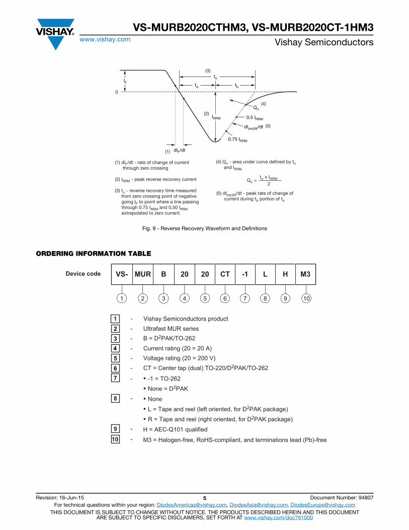
Fig. 9 - Reverse Recovery Waveform and Definitions
ORDERING INFORMATION TABLE
Qrr
0.5 IRRM
dI(rec)M/dt
0.75 IRRM
IRRM
trr
tbtaIF
dIF/dt
0
(1)
(2)
(3)
(4)
(5)
(1) dIF/dt - rate of change of current through zero crossing
(2) IRRM - peak reverse recovery current
(3) trr - reverse recovery time measured from zero crossing point of negative going IF to point where a line passing through 0.75 IRRM and 0.50 IRRM extrapolated to zero current.
(4) Qrr - area under curve defined by trr and IRRM
trr x IRRM 2
Qrr =
(5) dI(rec)M/dt - peak rate of change of current during tb portion of trr
2 - Ultrafast MUR series
3 - B = D2PAK/TO-262
4 - Current rating (20 = 20 A)5 - Voltage rating (20 = 200 V)
6 - CT = Center tap (dual) TO-220/D2PAK/TO-262
7 - -1 = TO-262
None = D2PAK8 - None
L = Tape and reel (left oriented, for D2PAK package)
9 - H = AEC-Q101 qualified
R = Tape and reel (right oriented, for D2PAK package)
Device code
51 32 4 6 7 8 9 10
VS- MUR B 20 20 CT -1 L H M3
1 - Vishay Semiconductors product
10 - M3 = Halogen-free, RoHS-compliant, and terminations lead (Pb)-free

VS-MURB2020CTHM3, VS-MURB2020CT-1HM3www.vishay.com Vishay Semiconductors
Revision: 16-Jun-15 6 Document Number: 94807For technical questions within your region: [email protected], [email protected], [email protected]
THIS DOCUMENT IS SUBJECT TO CHANGE WITHOUT NOTICE. THE PRODUCTS DESCRIBED HEREIN AND THIS DOCUMENTARE SUBJECT TO SPECIFIC DISCLAIMERS, SET FORTH AT www.vishay.com/doc?91000
ORDERING INFORMATION (Example)PREFERRED P/N QUANTITY PER TUBE MINIMUM ORDER QUANTITY PACKAGING DESCRIPTION
VS-MURB2020CTHM3 50 1000 Antistatic plastic tube
VS-MURB2020CT-1HM3 50 1000 Antistatic plastic tube
VS-MURB2020CTLHM3 800 800 13" diameter reel
VS-MURB2020CTRHM3 800 800 13" diameter reel
LINKS TO RELATED DOCUMENTS
DimensionsTO-263AB (D2PAK) www.vishay.com/doc?95046
TO-262AA www.vishay.com/doc?95419
Part marking informationTO-263AB (D2PAK) www.vishay.com/doc?95444
TO-262AA www.vishay.com/doc?95443
Packaging information TO-263AB (D2PAK) www.vishay.com/doc?95032
SPICE model www.vishay.com/doc?95622
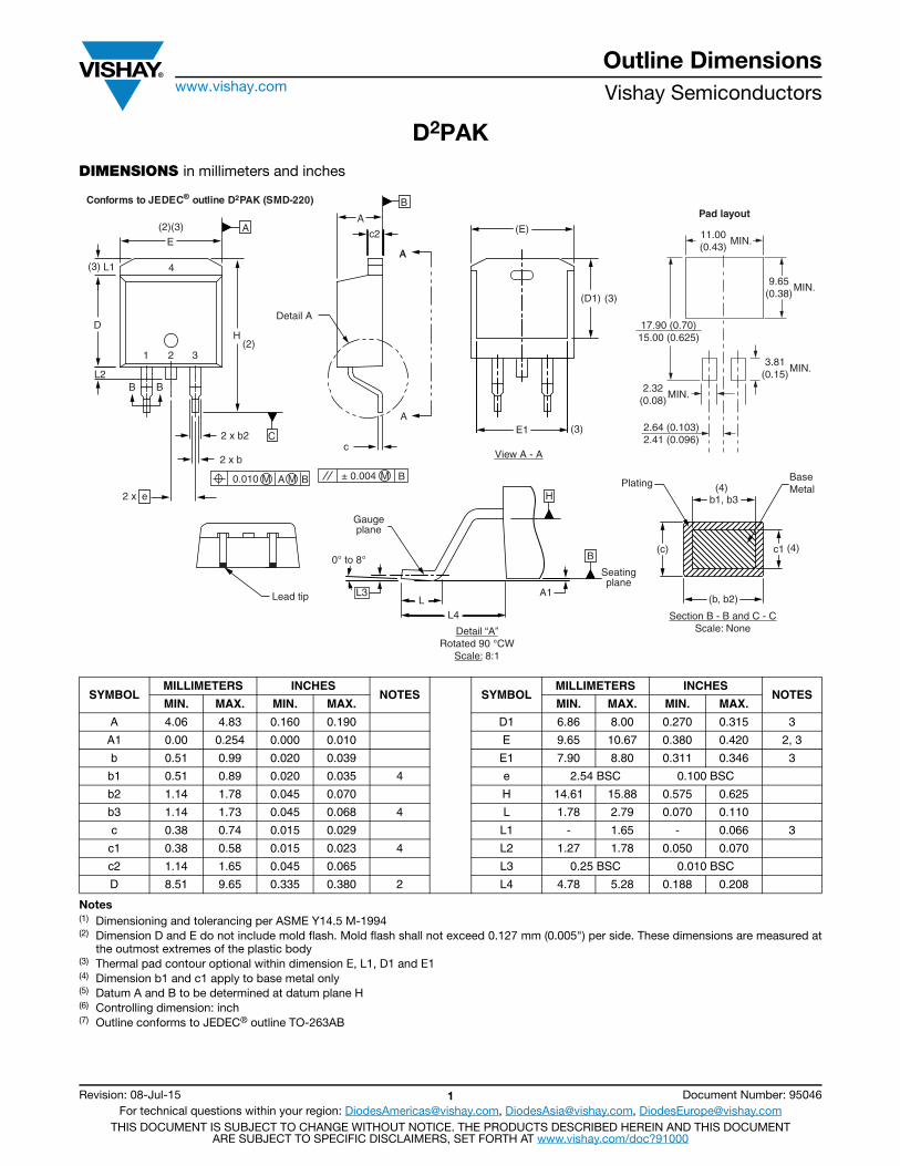
Outline Dimensionswww.vishay.com Vishay Semiconductors
Revision: 08-Jul-15 1 Document Number: 95046For technical questions within your region: [email protected], [email protected], [email protected]
THIS DOCUMENT IS SUBJECT TO CHANGE WITHOUT NOTICE. THE PRODUCTS DESCRIBED HEREIN AND THIS DOCUMENTARE SUBJECT TO SPECIFIC DISCLAIMERS, SET FORTH AT www.vishay.com/doc?91000
D2PAK
DIMENSIONS in millimeters and inches
Notes(1) Dimensioning and tolerancing per ASME Y14.5 M-1994(2) Dimension D and E do not include mold flash. Mold flash shall not exceed 0.127 mm (0.005") per side. These dimensions are measured at
the outmost extremes of the plastic body(3) Thermal pad contour optional within dimension E, L1, D1 and E1(4) Dimension b1 and c1 apply to base metal only(5) Datum A and B to be determined at datum plane H(6) Controlling dimension: inch(7) Outline conforms to JEDEC® outline TO-263AB
SYMBOLMILLIMETERS INCHES
NOTES SYMBOLMILLIMETERS INCHES
NOTESMIN. MAX. MIN. MAX. MIN. MAX. MIN. MAX.
A 4.06 4.83 0.160 0.190 D1 6.86 8.00 0.270 0.315 3
A1 0.00 0.254 0.000 0.010 E 9.65 10.67 0.380 0.420 2, 3
b 0.51 0.99 0.020 0.039 E1 7.90 8.80 0.311 0.346 3
b1 0.51 0.89 0.020 0.035 4 e 2.54 BSC 0.100 BSC
b2 1.14 1.78 0.045 0.070 H 14.61 15.88 0.575 0.625
b3 1.14 1.73 0.045 0.068 4 L 1.78 2.79 0.070 0.110
c 0.38 0.74 0.015 0.029 L1 - 1.65 - 0.066 3
c1 0.38 0.58 0.015 0.023 4 L2 1.27 1.78 0.050 0.070
c2 1.14 1.65 0.045 0.065 L3 0.25 BSC 0.010 BSC
D 8.51 9.65 0.335 0.380 2 L4 4.78 5.28 0.188 0.208
c
B
Detail A
c2
AA
A
± 0.004 BM
A
Lead tip
(3)
(3)
View A - A
(E)
(D1)
E1
B
H
A1
Detail “A”Rotated 90 °CW
Scale: 8:1
L
Gaugeplane
0° to 8°
L3
L4
Seatingplane
Section B - B and C - CScale: None
(4)
(4)
(b, b2)
b1, b3
(c) c1
BaseMetal
Plating
Conforms to JEDEC® outline D2PAK (SMD-220)
1 32
D
C
A
L2
E
(2)(3)
(2)
4
H
B B
2 x b
2 x b2
L1
0.010 A BM M
(3)
e2 x
Pad layout
MIN.11.00(0.43)
MIN.9.65
(0.38)
MIN.3.81
(0.15)
MIN.2.32
(0.08)
17.90 (0.70)15.00 (0.625)
2.64 (0.103)2.41 (0.096)

Document Number: 95419 For technical questions within your region, please contact one of the following: www.vishay.comRevision: 04-Oct-10 [email protected], [email protected], [email protected] 1
TO-262
Outline DimensionsVishay Semiconductors
DIMENSIONS in millimeters and inches
Notes(1) Dimensioning and tolerancing as per ASME Y14.5M-1994(2) Dimension D and E do not include mold flash. Mold flash shall
not exceed 0.127 mm (0.005") per side. These dimensions aremeasured at the outmost extremes of the plastic body
(3) Thermal pad contour optional within dimension E, L1, D1 and E1
(4) Dimension b1 and c1 apply to base metal only(5) Controlling dimension: inches(6) Outline conform to JEDEC TO-262 except A1 (maximum), b
(minimum) and D1 (minimum) where dimensions derived theactual package outline
SYMBOLMILLIMETERS INCHES
NOTESMIN. MAX. MIN. MAX.
A 4.06 4.83 0.160 0.190
A1 2.03 3.02 0.080 0.119
b 0.51 0.99 0.020 0.039
b1 0.51 0.89 0.020 0.035 4
b2 1.14 1.78 0.045 0.070
b3 1.14 1.73 0.045 0.068 4
c 0.38 0.74 0.015 0.029
c1 0.38 0.58 0.015 0.023 4
c2 1.14 1.65 0.045 0.065
D 8.51 9.65 0.335 0.380 2
D1 6.86 8.00 0.270 0.315 3
E 9.65 10.67 0.380 0.420 2, 3
E1 7.90 8.80 0.311 0.346 3
e 2.54 BSC 0.100 BSC
L 13.46 14.10 0.530 0.555
L1 - 1.65 - 0.065 3
L2 3.56 3.71 0.140 0.146
(4)
(4) BasemetalPlating b1, b3
(b, b2)
c1c
Section B - B and C - CScale: None
Section A - A
(3)E1
(3)D1
EBA
A
A
c2
c
A1
Seatingplane
Lead tip
(3)
(2) (3)
(2)
AE(Datum A)
L1
L2
B B
C C
321
L
D
2 x e
3 x b23 x b
0.010 A BM M
Modified JEDEC outline TO-262
Lead assignments
Diodes1. - Anode (two die)/open (one die)2., 4. - Cathode3. - Anode

Legal Disclaimer Noticewww.vishay.com Vishay
Revision: 02-Oct-12 1 Document Number: 91000
DisclaimerALL PRODUCT, PRODUCT SPECIFICATIONS AND DATA ARE SUBJECT TO CHANGE WITHOUT NOTICE TO IMPROVERELIABILITY, FUNCTION OR DESIGN OR OTHERWISE.
Vishay Intertechnology, Inc., its affiliates, agents, and employees, and all persons acting on its or their behalf (collectively,“Vishay”), disclaim any and all liability for any errors, inaccuracies or incompleteness contained in any datasheet or in any otherdisclosure relating to any product.
Vishay makes no warranty, representation or guarantee regarding the suitability of the products for any particular purpose orthe continuing production of any product. To the maximum extent permitted by applicable law, Vishay disclaims (i) any and allliability arising out of the application or use of any product, (ii) any and all liability, including without limitation special,consequential or incidental damages, and (iii) any and all implied warranties, including warranties of fitness for particularpurpose, non-infringement and merchantability.
Statements regarding the suitability of products for certain types of applications are based on Vishay’s knowledge of typicalrequirements that are often placed on Vishay products in generic applications. Such statements are not binding statementsabout the suitability of products for a particular application. It is the customer’s responsibility to validate that a particularproduct with the properties described in the product specification is suitable for use in a particular application. Parametersprovided in datasheets and/or specifications may vary in different applications and performance may vary over time. Alloperating parameters, including typical parameters, must be validated for each customer application by the customer’stechnical experts. Product specifications do not expand or otherwise modify Vishay’s terms and conditions of purchase,including but not limited to the warranty expressed therein.
Except as expressly indicated in writing, Vishay products are not designed for use in medical, life-saving, or life-sustainingapplications or for any other application in which the failure of the Vishay product could result in personal injury or death.Customers using or selling Vishay products not expressly indicated for use in such applications do so at their own risk. Pleasecontact authorized Vishay personnel to obtain written terms and conditions regarding products designed for such applications.
No license, express or implied, by estoppel or otherwise, to any intellectual property rights is granted by this document or byany conduct of Vishay. Product names and markings noted herein may be trademarks of their respective owners.
Material Category PolicyVishay Intertechnology, Inc. hereby certifies that all its products that are identified as RoHS-Compliant fulfill thedefinitions and restrictions defined under Directive 2011/65/EU of The European Parliament and of the Councilof June 8, 2011 on the restriction of the use of certain hazardous substances in electrical and electronic equipment(EEE) - recast, unless otherwise specified as non-compliant.
Please note that some Vishay documentation may still make reference to RoHS Directive 2002/95/EC. We confirm thatall the products identified as being compliant to Directive 2002/95/EC conform to Directive 2011/65/EU.
Vishay Intertechnology, Inc. hereby certifies that all its products that are identified as Halogen-Free follow Halogen-Freerequirements as per JEDEC JS709A standards. Please note that some Vishay documentation may still make referenceto the IEC 61249-2-21 definition. We confirm that all the products identified as being compliant to IEC 61249-2-21conform to JEDEC JS709A standards.