ultrafast and nanoscale plasmonic phenomena in exfoliated...
TRANSCRIPT

Ultrafast and Nanoscale Plasmonic Phenomena in ExfoliatedGraphene Revealed by Infrared Pump−Probe NanoscopyMartin Wagner,† Zhe Fei,† Alexander S. McLeod,† Aleksandr S. Rodin,†,# Wenzhong Bao,‡,§
Eric G. Iwinski,† Zeng Zhao,§ Michael Goldflam,† Mengkun Liu,† Gerardo Dominguez,∥,⊥
Mark Thiemens,⊥ Michael M. Fogler,† Antonio H. Castro Neto,¶,# Chun Ning Lau,§ Sergiu Amarie,□
Fritz Keilmann,■ and D. N. Basov*,†
†Department of Physics, University of California, San Diego, La Jolla, California 92093, United States#Department of Physics, Boston University, 590 Commonwealth Avenue, Boston, Massachusetts 02215, United States‡Materials Research Science and Engineering Center, University of Maryland, College Park, Maryland 20742, United States§Department of Physics and Astronomy, University of California, Riverside, California 92521, United States∥Department of Physics, California State University, San Marcos, San Marcos, California 92096, United States⊥Department of Chemistry and Biochemistry, University of California, San Diego, La Jolla, California 92093, United States¶Graphene Research Centre and Department of Physics, National University of Singapore, 117542, Singapore□Neaspec GmbH, Bunsenstrasse 5, 82152 Martinsried, Munchen, Germany■Ludwig-Maximilians-Universitat and Center for Nanoscience, 80539 Munchen, Germany
*S Supporting Information
ABSTRACT: Pump−probe spectroscopy is central for exploring ultrafastdynamics of fundamental excitations, collective modes, and energy transferprocesses. Typically carried out using conventional diffraction-limited optics,pump−probe experiments inherently average over local chemical, compositional,and electronic inhomogeneities. Here, we circumvent this deficiency and introducepump−probe infrared spectroscopy with ∼20 nm spatial resolution, far below thediffraction limit, which is accomplished using a scattering scanning near-fieldoptical microscope (s-SNOM). This technique allows us to investigate exfoliatedgraphene single-layers on SiO2 at technologically significant mid-infrared (MIR)frequencies where the local optical conductivity becomes experimentally accessiblethrough the excitation of surface plasmons via the s-SNOM tip. Optical pumping atnear-infrared (NIR) frequencies prompts distinct changes in the plasmonicbehavior on 200 fs time scales. The origin of the pump-induced, enhancedplasmonic response is identified as an increase in the effective electron temperature up to several thousand Kelvin, as deduceddirectly from the Drude weight associated with the plasmonic resonances.
KEYWORDS: Graphene, Dirac plasmon, pump−probe, time-resolved spectroscopy, near-field microscopy, s-SNOM
Graphene is emerging as a promising system foroptoelectronic and plasmonic applications.1−4 This is in
part because the optical, electronic, and plasmonic phenomenapresent in graphene are amenable to modifications by chemicaldoping and electrostatic gating. Specifically, these stimuliinfluence both the amplitude and the wavelength of Diracplasmons, the surface charge oscillations in graphene.5,6
Tunable surface plasmons are of high interest in the contextof confining and controlling long-wavelength electromagneticradiation at the length scales typical of X-rays.7 The key noveltyof the results presented here is that the plasmonic effects ingraphene can be modified on ultrafast time scales with anefficiency rivaling that of electrostatic gating. This is achievedusing a novel approach that enables pump−probe spectroscopyin the infrared (IR) region with nanoscale spatial resolution.
Common optical pump−probe experiments have beenextensively employed to investigate fundamental physicaleffects in condensed matter.8,9 However, the spatial resolutionof these techniques is typically limited by diffraction restrictingthe minimum sampling area to about 1 μm2 for measurementsin the visible and to 102−104 μm2 or more for IR and terahertz(THz) studies. For that reason, pump−probe experiments ongraphene have been performed on large area samples10−13 thatare prone to the formation of various defects or grainboundaries14,15 obscuring intrinsic electronic and opticalphenomena. These irregularities are absent in exfoliated
Received: November 17, 2013Revised: January 5, 2014Published: January 30, 2014
Letter
pubs.acs.org/NanoLett
© 2014 American Chemical Society 894 dx.doi.org/10.1021/nl4042577 | Nano Lett. 2014, 14, 894−900

graphene with typical dimensions smaller than the wavelengthof IR light: the type of specimens we investigated in ourexperiments.Here, we implemented a nanospectroscopic IR local probe
via s-SNOM16,17 under intense near-infrared (NIR) laserexcitation. We employed this new technique to explore theultrafast response of Dirac plasmons in graphene. Our keyobservation pertains to strong enhancement of plasmonicfeatures by NIR pumping, which we directly monitor in ourtime-resolved spectra. We can fully account for this behavior bymodeling NIR pumping as light-induced heating of the free-carrier subsystem of graphene. Specifically, we show that theintraband Drude weight D due to Dirac quasiparticles increaseswith their effective carrier temperature even though the densityof electrons in the system, that is, the number of electrons inthe conduction band minus the number of holes in the valenceband, remains unchanged under NIR illumination. We stressthat the Drude weight is directly accessible in our measure-ments through the analysis of the plasmonic features in theinfrared spectra that we collect with the 200 fs temporalresolution. Furthermore, our data attest to the ability tooptically modify Dirac plasmons on 20 nm length scales and200 fs time scales. An important virtue of our approach is thatthe conversion of light to electron−hole pairs can now beinvestigated at length scales characteristic of these light-matterinteraction processes and of prototypical photonics/plasmonicsdevices.1,2,4,7,18,19
Our setup (Figure 1a) integrates a commercial s-SNOM(Neaspec GmbH) with a mid-infrared (MIR) source (Lasnix)
emitting ultrashort (<100 fs) pulses based on a 40 MHz NIRfiber laser (Toptica Photonics, Inc.).20−22 We note that owingto field enhancement by the s-SNOM tip23 an in-plane MIRpeak field strength of the order of 102 kV/cm can be obtainedwith such a relatively low-cost, high repetition rate laser system(see Supporting Information). Ultrafast temporal resolution isachieved by operating the s-SNOM in pump−probe modewhereby the synchronized 100 fs NIR pulses of the fiber laserserve as 1.56 μm pump light with variable delay. Exfoliatedgraphene samples on 300 nm SiO2 were studied at ambientconditions. Raman spectroscopy confirmed an unintentional
hole-doping |n| = (2.6 ± 1) × 1012 cm−2, corresponding to achemical potential μ0 = −(1500 ± 300) cm−1.The near-field response of graphene on SiO2 in the MIR
region is dominated by hybrid resonances originating from thecoupling of plasmons to the surface phonon modes of thesubstrate.24 We first consider these plasmonic features in thenear-field data in the absence of the NIR excitation. In Figure2a, we plot s(ω) spectra: the second harmonic of the near field
scattering amplitude s2 normalized to that of silicon. The s(ω)spectrum of SiO2 alone (black curve in Figure 2a) is dominatedby two surface phonons denoted as α and β, giving rise to astrong peak at ωα = 1125 cm−1 and a weaker one at ωβ = 785cm−1.25 A single layer of graphene modifies the main features ofthe SiO2 substrate response (red curve). We register a 5 cm−1
blueshift of the α resonance compared to SiO2 and abroadening of its high-frequency shoulder, effects rooted in
Figure 1. (a) Sketch of the NIR pump MIR probe near-fieldspectroscopy experiment on exfoliated graphene. (b) MIR spectros-copy data were acquired with probe pulses forming these twooverlapping, broad-band spectra.
Figure 2. Graphene near-field spectra with and without NIRphotoexcitation. (a) Near-field amplitude MIR spectra s(ω) (withoutNIR excitation) normalized to Si, for 300 nm SiO2 (black curve) andfor single-layer graphene on SiO2 (red curve, probed with attenuatedMIR intensity). The SiO2 phonon modes at ωα = 1125 cm−1 and ωβ =785 cm−1 are labeled as α and β. (b) NIR pump-induced, spectralchanges in the near-field amplitude Δs(ω)/s(ω) of graphene at zerotime delay for varying NIR average powers. The effect of electrostaticgating (without NIR pumping) is shown for comparison. The inset ofpanel (b) displays Δs(ω)/s(ω) for different graphene films at 10 mWpump power. (c) Theoretical effect of increasing the intraband Drudeweight D above the initial nonequilibrium value 1.10D0 that serves asreference without NIR pump in intense MIR probe fields. While NIRpumping effects were modeled by an increase in carrier temperature,gating effects were simulated by adjusting the Fermi energy.
Nano Letters Letter
dx.doi.org/10.1021/nl4042577 | Nano Lett. 2014, 14, 894−900895

the interaction of the surface phonons of the SiO2 substratewith the Dirac plasmons in graphene.24 Note that theplasmon−phonon coupling is fundamentally a finite momen-tum effect (see dispersion plot in Figure 3a). The ability ofnear-field nanoscopy to investigate this effect stems from theAFM tip providing access to momenta of the order of qtip ∼ 1/a(vertical dashed lines in Figure 3a,b) where a is the tip radius.24
Thus, we are able to study surface plasmons in pristine,exfoliated graphene. We note that plasmonic coupling in far-field experiments requires nanostructuring of large-area CVD orepitaxial samples26 prone to defects inherent to bothgrowth14,15 and patterning26 procedures.Because our inquiry into the ultrafast plasmon dynamics
relies on monitoring the hybrid plasmon−phonon resonances,we discuss the dispersion relationships unraveling the physics ofthis coupling to set the stage for later analysis of the pump−probe data. The dispersion of the Dirac plasmon alone (redcurves in Figure 3a,b) and of the hybrid plasmon−phononmodes (color plots in Figure 3a,b) is calculated24 based on thestandard sheet conductivity of graphene comprising intra- andinterband components as
σ ω σ ω σ ω σ ωπ ω γ
= + =+
i Di
( ) ( ) ( ), ( )intra inter intra
(1)
The plasmonic response of graphene is dominated by theintraband part that is defined by two parameters: the Drudeweight D and the scattering rate γ.27 Ignoring for a moment theimpact of the substrate, the dispersion of the plasmon (redcurves in Figure 3a,b) follows the familiar square-root behaviorω ∼ (kFq)
1/2 for q values below the Fermi wavevector kF. Thehorizontal lines in Figure 3a,b denote the SiO2 surfacephonons, defined by Re κ(ω) = 0, where κ(ω) = (1 +εSiO2
(ω))/2 is the arithmetic mean of the dielectric functions ofair and SiO2. Once coupling between the plasmon and SiO2phonons is taken into account, the dispersion is dominated byavoided crossings. An immediate consequence of the couplingis the blueshift of the α resonance that is consistent with thedata in Figure 2a.Next, we examine the influence of NIR pumping on the
graphene response at zero time delay between pump and probepulses. We present pump-induced changes of the scatteringamplitude Δs(ω)/s(ω) (Figure 2b), collected from a ∼10−20
nm spot that is defined by the radius of the tip. The spectrashow an increase of the scattering amplitude, which isparticularly pronounced at frequencies just above the α and βmodes, amounting to as much as 20% around ω = 1200 cm−1.The upper frequency cutoff in Figure 2b is governed by thesignal-to-noise of our data. At ω = 900 cm−1, a weaker andbroader peak appears whereas the β mode is only marginallyamplified. Multilayer graphene shows a stronger photoinducedresponse (see inset of Figure 2b) that grows nearly linearly withthe number of layers.Diffraction-limited pump−probe experiments on graphene
have established several facts relevant to our nanoscaleobservations.12,13,28,29 Immediately after photoexcitation gra-phene reveals distinct electron and hole chemical potentialsthat last only 10−30 fs after the pump pulse arrives. Interbandscattering of electrons and holes occurs via Auger and carriermultiplication processes that are kinematically allowed andefficient in graphene. The net effect is that 30 fs after the pumppulse is incident on graphene, electrons and holes arecharacterized by a single Fermi-Dirac distribution with thesame effective temperature T and chemical potential μ(T).12,28
The 200 fs temporal resolution of our apparatus only enablesaccess to the latter regime of “hot electrons” whereas the effectsof rapid equilibration are beyond our range.Remarkably, the spectral changes associated with pump-
induced heating of electrons in single-layer graphene closelyresemble those originating from electrostatic gating. As shownin Figure 2b (dots), similar Δs(ω)/s(ω) spectra are obtained byapplying a gate voltage of Vg = −70 V and thus increasing thesample’s hole-doping. To the best of our knowledge, data inFigure 2b is the first attempt to explicitly compare spectralfeatures induced in graphene by gating and ultrafast photo-excitation. We were able to account for this peculiar similarityof the response to the two distinct stimuli within our intrabandDrude model of plasmonic response introduced in thefollowing section.We now proceed to our quantitative description of the
plasmonic response in the regime of pump-induced heating ofthe electronic system based on eq 1 and introduce atemperature dependent intraband Drude weight (Figure 3c)in the following form:30
Figure 3. Calculated plasmon−phonon mode dispersion and Drude weight. (a) Graphene plasmon SiO2 phonon mode dispersion evaluated as theimaginary part of the reflection coefficient rp (q, ω) = 1 − (κ(ω) + 2πiσq/ω)−1. The vertical dashed line marks the probe wavevector qtip ∼ 1/a (a =40 nm), the horizontal lines denote the α and β SiO2 phonons, and the red curve represents the graphene plasmon without phonon interaction. Thecalculated dispersion curves for the case of phonon interaction are given for the indicated Drude weight D and scattering rate γ corresponding toattenuated MIR intensity. (b) Full MIR probe intensity and synchronous 10 mW NIR pumping, characterized by an increase in D and γ. (c)Theoretical, nonmonotonic temperature dependence of D and μ normalized to their T = 300 K or equilibrium values. The values of D obtained bymodeling the experimental NIR pump induced spectral changes of Figure 2b are marked with the corresponding carrier temperature T, showing thatT and D increase for NIR pumping. The minimum in D (open dot) is marked together with the position where the equilibrium value D = D0 isrecovered (black square).
Nano Letters Letter
dx.doi.org/10.1021/nl4042577 | Nano Lett. 2014, 14, 894−900896

μ=ℏ
⎛⎝⎜
⎞⎠⎟
⎡⎣⎢⎢
⎛⎝⎜
⎞⎠⎟⎤⎦⎥⎥D
ek T
k T2
ln 2cosh2
2
2 BB (2)
In the zero-temperature limit eq 2 reduces to D = (e2/ℏ2) μ ∝(|n|)1/2 where n is the carrier density,27 that is, the electronconcentration in the conduction band minus the holeconcentration in the valence band. At elevated temperatures,kBT ≫ μ, eq 2 implies a linear dependence D ∝ T (asymptotein Figure 3c). Counterintuitively, for T ≠ 0 a peculiar situationcan arise: D increases with temperature although the density ofelectrons in the system n is constant,31 a scenario relevant tothe photoinduced heating of our graphene samples. The neteffect of high electron temperature is that the plasmonicresponse of graphene at IR frequencies is enhanced as we willshow below.The Drude model of plasmonic response grasps the gross
features of both the transient and the equilibrium data in Figure2. At equilibrium (Figure 2a), this model accounts for thespectral features associated with both the α and β plasmon−phonon modes assuming γ = 100 cm−1 and the Drude weightD0 = 24.3|μ0|σ0/ℏ (see Figure S2 in Supporting Information).Here σ0 = e2/(4ℏ) denotes the so-called universal conductivityof graphene. Owing to small signal-to-noise ratios the full MIRintensity with an in-plane field strength of the order of 102 kV/cm is necessary to carry out the pump−probe experiment (seeSupporting Information). This results in an increase of theDrude weight up to DMIR = 1.10D0 which can be attributed tothe elevated electron temperature T = 1500 K according to eq2.28,32 Nevertheless, in the absence of NIR pumping, thedominant effect in the spectra (see Figure S2 in the SupportingInformation) is due to the 3-fold increase of the scattering rateto γ = 300 cm−1.33 An increase in carrier temperaturedominates in our NIR pumping results. Specifically, we wereable to reproduce the pump-induced enhancement of the near-field amplitude at ω > 1050 cm−1 with the following values forD: D2mW = 1.21D0, D5mW = 1.33D0, and D10mW = 1.46D0 (blue,red, and black line in Figure 2c). The full set of modelingparameters is presented in Table 1. We found that the modelspectra capture the essential aspects of our data even if we keepthe scattering rate constant at γ = 300 cm−1 for any NIRillumination power. At frequencies below 1000 cm−1, there is aslight mismatch between the details of the experimental andtheoretical spectra. The simulation correctly replicates a peak inthe vicinity of the β mode. However, the peak width is smalleras compared to experimental data. The net result of thesesimulations is that hot electrons in graphene (with an effectivetemperature in excess of 2000 K) lead to significantenhancement of the plasmonic resonance. Electrostatic gatingis replicated in our modeling by tuning the Fermi energy atconstant temperature (T = 1500 K) and scattering rate (γ =300 cm−1), yielding the Drude weight of 1.46D0, similar to the
case of 10 mW optical excitation. The corresponding gate-induced carrier density of |Δn| = 4.2 × 1012 cm−2 is close to theexperimental value of 5 × 1012 cm−2 estimated from thecommon capacitor model for the applied gate voltage Vg = −70V.34 However, under ambient conditions the charge-neutralitypoint is known to shift in electrostatic gating.35 Consequently,the actual carrier density in our gating experiment can beexpected to differ from the value inferred from the capacitormodel, especially in the unexplored regime of additional,intense MIR illumination.It is instructive to discuss the response of hot electrons and
plasmons in graphene under NIR pumping in terms of theplasmon−phonon dispersion relations (Figure 3a,b). In Figure3a we plot the dispersion under equilibrium conditionscorresponding to the intraband Drude weight D0. Thedispersion in Figure 3b represents the pump-induced non-equilibrium situation and is different from the dispersion inFigure 3a in two ways. First, the dispersion traces arebroadened by excessive damping (γ = 300 cm−1) caused bythe hot electron temperature as in the case of pure MIRpumping at full intensity (see Supporting Information).Second, the Drude weight governing the behavior of theplasmonic branch is increased by nearly 50% compared to theequilibrium value. The elevated Drude weight increases theslope of the plasmon dispersion (red line). Enhanced overlapwith the SiO2 phonon modes leads to a blueshift of both the αand β resonances at q ∼ qtip. Thus, spectral changes induced byNIR pumping indeed are expected to be similar to thoseoriginating from electrostatic gating despite the assumption ofconstant electron density in our modeling. Note that intense in-plane dc fields have recently been predicted to increase theslope of the plasmon dispersion.36 However, this is a higher-order effect that is not expected to play a significant role in ourcase. That is because in our experiments the ac electric fieldsaverage to zero both in time and due to the radial fielddistribution directly under the tip also in space.We stress that even though μ(T) is suppressed at elevated
temperatures (Figure 3c), the Drude weight D is enhancedabove its equilibrium value D0 for T > 0.60 |μ0|/kB = 1270 K(black square). The sensitivity of the Drude weight to theelectron temperature enables ultrafast optical control ofplasmonic effects in graphene at femtosecond time scales.Since D defines both the amplitude and wavelength of surfaceplasmons in graphene, both of these fundamental characteristicswill be impacted by photoexcitation.5,6
For bi- and trilayer graphene, similar behavior showingenhanced intraband Drude weight with temperature is expectedwhen the electron temperature kBT approaches (or exceeds)the interlayer tunneling energy γ1 = 0.4 eV, a situation close toour experimental parameters. An approximately linear dis-persion in that region should mimic the temperature depend-ence of D in single-layer graphene. Data in the inset of Figure
Table 1. Summary of the Modeling Parameters for the Drude Model of Plasmonic Response
equilibrium:weak MIR excitation
nonequilibrium:strong MIR excitation
+ gating + NIR excitation with power ...
2 mW 5 mW 10 mW
Drude weight D D0a 1.10D0 1.46D0 1.21D0 1.33D0 1.46D0
T (K) 300 1500 1500 1700 1900 2100γ (cm−1) 100 300 300 300 300 300
aD0 = 24.3|μ0|σ0/ℏ with universal conductivity σ0 = e2/(4ℏ) and |μ0| = 1500 cm−1.
Nano Letters Letter
dx.doi.org/10.1021/nl4042577 | Nano Lett. 2014, 14, 894−900897
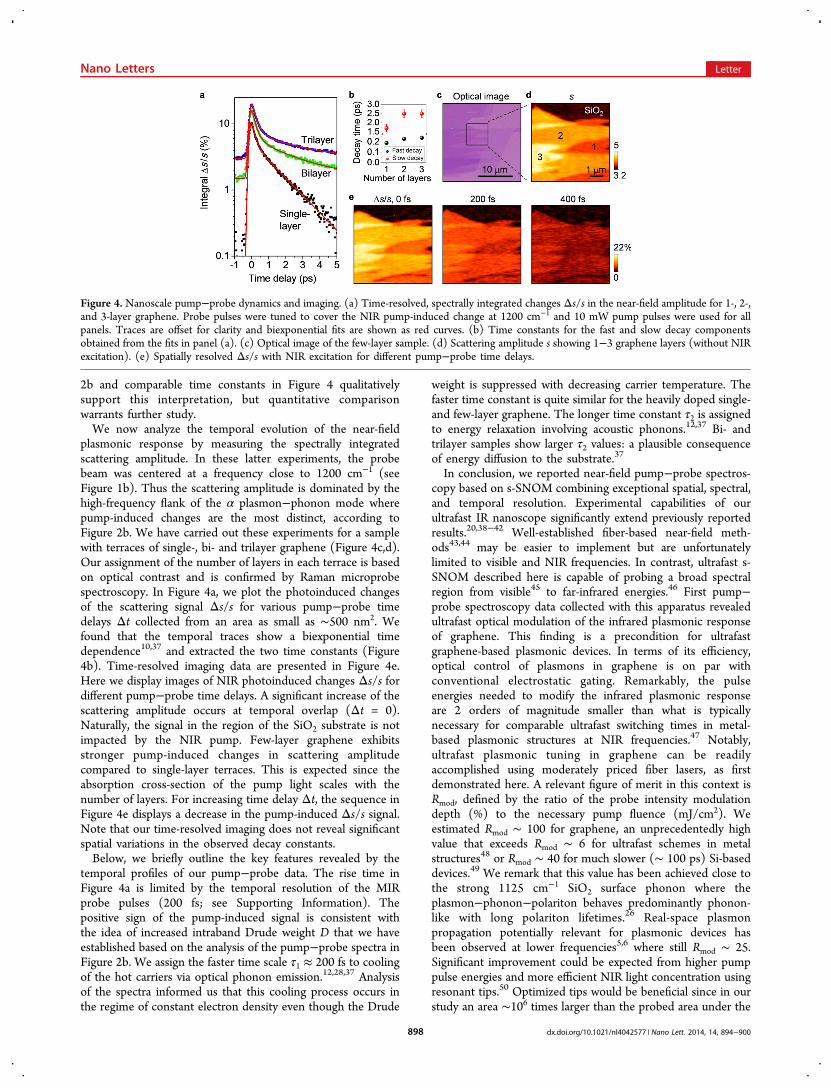
2b and comparable time constants in Figure 4 qualitativelysupport this interpretation, but quantitative comparisonwarrants further study.We now analyze the temporal evolution of the near-field
plasmonic response by measuring the spectrally integratedscattering amplitude. In these latter experiments, the probebeam was centered at a frequency close to 1200 cm−1 (seeFigure 1b). Thus the scattering amplitude is dominated by thehigh-frequency flank of the α plasmon−phonon mode wherepump-induced changes are the most distinct, according toFigure 2b. We have carried out these experiments for a samplewith terraces of single-, bi- and trilayer graphene (Figure 4c,d).Our assignment of the number of layers in each terrace is basedon optical contrast and is confirmed by Raman microprobespectroscopy. In Figure 4a, we plot the photoinduced changesof the scattering signal Δs/s for various pump−probe timedelays Δt collected from an area as small as ∼500 nm2. Wefound that the temporal traces show a biexponential timedependence10,37 and extracted the two time constants (Figure4b). Time-resolved imaging data are presented in Figure 4e.Here we display images of NIR photoinduced changes Δs/s fordifferent pump−probe time delays. A significant increase of thescattering amplitude occurs at temporal overlap (Δt = 0).Naturally, the signal in the region of the SiO2 substrate is notimpacted by the NIR pump. Few-layer graphene exhibitsstronger pump-induced changes in scattering amplitudecompared to single-layer terraces. This is expected since theabsorption cross-section of the pump light scales with thenumber of layers. For increasing time delay Δt, the sequence inFigure 4e displays a decrease in the pump-induced Δs/s signal.Note that our time-resolved imaging does not reveal significantspatial variations in the observed decay constants.Below, we briefly outline the key features revealed by the
temporal profiles of our pump−probe data. The rise time inFigure 4a is limited by the temporal resolution of the MIRprobe pulses (200 fs; see Supporting Information). Thepositive sign of the pump-induced signal is consistent withthe idea of increased intraband Drude weight D that we haveestablished based on the analysis of the pump−probe spectra inFigure 2b. We assign the faster time scale τ1 ≈ 200 fs to coolingof the hot carriers via optical phonon emission.12,28,37 Analysisof the spectra informed us that this cooling process occurs inthe regime of constant electron density even though the Drude
weight is suppressed with decreasing carrier temperature. Thefaster time constant is quite similar for the heavily doped single-and few-layer graphene. The longer time constant τ2 is assignedto energy relaxation involving acoustic phonons.12,37 Bi- andtrilayer samples show larger τ2 values: a plausible consequenceof energy diffusion to the substrate.37
In conclusion, we reported near-field pump−probe spectros-copy based on s-SNOM combining exceptional spatial, spectral,and temporal resolution. Experimental capabilities of ourultrafast IR nanoscope significantly extend previously reportedresults.20,38−42 Well-established fiber-based near-field meth-ods43,44 may be easier to implement but are unfortunatelylimited to visible and NIR frequencies. In contrast, ultrafast s-SNOM described here is capable of probing a broad spectralregion from visible45 to far-infrared energies.46 First pump−probe spectroscopy data collected with this apparatus revealedultrafast optical modulation of the infrared plasmonic responseof graphene. This finding is a precondition for ultrafastgraphene-based plasmonic devices. In terms of its efficiency,optical control of plasmons in graphene is on par withconventional electrostatic gating. Remarkably, the pulseenergies needed to modify the infrared plasmonic responseare 2 orders of magnitude smaller than what is typicallynecessary for comparable ultrafast switching times in metal-based plasmonic structures at NIR frequencies.47 Notably,ultrafast plasmonic tuning in graphene can be readilyaccomplished using moderately priced fiber lasers, as firstdemonstrated here. A relevant figure of merit in this context isRmod, defined by the ratio of the probe intensity modulationdepth (%) to the necessary pump fluence (mJ/cm2). Weestimated Rmod ∼ 100 for graphene, an unprecedentedly highvalue that exceeds Rmod ∼ 6 for ultrafast schemes in metalstructures48 or Rmod ∼ 40 for much slower (∼ 100 ps) Si-baseddevices.49 We remark that this value has been achieved close tothe strong 1125 cm−1 SiO2 surface phonon where theplasmon−phonon−polariton behaves predominantly phonon-like with long polariton lifetimes.26 Real-space plasmonpropagation potentially relevant for plasmonic devices hasbeen observed at lower frequencies5,6 where still Rmod ∼ 25.Significant improvement could be expected from higher pumppulse energies and more efficient NIR light concentration usingresonant tips.50 Optimized tips would be beneficial since in ourstudy an area ∼106 times larger than the probed area under the
Figure 4. Nanoscale pump−probe dynamics and imaging. (a) Time-resolved, spectrally integrated changes Δs/s in the near-field amplitude for 1-, 2-,and 3-layer graphene. Probe pulses were tuned to cover the NIR pump-induced change at 1200 cm−1 and 10 mW pump pulses were used for allpanels. Traces are offset for clarity and biexponential fits are shown as red curves. (b) Time constants for the fast and slow decay componentsobtained from the fits in panel (a). (c) Optical image of the few-layer sample. (d) Scattering amplitude s showing 1−3 graphene layers (without NIRexcitation). (e) Spatially resolved Δs/s with NIR excitation for different pump−probe time delays.
Nano Letters Letter
dx.doi.org/10.1021/nl4042577 | Nano Lett. 2014, 14, 894−900898

tip was illuminated and the total amount of NIR fieldenhancement is unclear (see Supporting Information). Never-theless, this first infrared pump−probe experiment beyond thediffraction limit demonstrates the capability of this techniqueand paves the way to the exploration of a wide range ofproblems in condensed matter physics, biology, and chemistry.
■ ASSOCIATED CONTENT*S Supporting InformationSupporting experimental data and theory details. This materialis available free of charge via the Internet at http://pubs.acs.org.
■ AUTHOR INFORMATIONCorresponding Author*E-mail: [email protected] authors declare the following competing financialinterest(s): F. K. is cofounder of Neaspec and Lasnix, producersof the s-SNOM and infrared source used in this study. All otherauthors declare no competing financial interests.
■ ACKNOWLEDGMENTSM.W. acknowledges financial support by the Alexander vonHumboldt foundation. Research at UCSD is supported byONR. The development of near-field instrumentation at UCSDis supported by DOE-BES. A.S.R. and A.H.C.N. acknowledgeDOE grant DE-FG02-08ER46512, ONR grant MURI N00014-09-1-1063, and the NRF-CRP award R-144-000-295-281.
■ REFERENCES(1) Bonaccorso, F.; Sun, Z.; Hasan, T.; Ferrari, A. C. Nat. Photonics2010, 4, 611−622.(2) Bao, Q.; Loh, K. P. ACS Nano 2012, 6, 3677−3694.(3) Koppens, F. H. L.; Chang, D. E.; García de Abajo, F. J. Nano Lett.2011, 11, 3370−3377.(4) Grigorenko, A. N.; Polini, M.; Novoselov, K. S. Nat. Photonics2012, 6, 749−758.(5) Fei, Z.; Rodin, A. S.; Andreev, G. O.; Bao, W.; McLeod, A. S.;Wagner, M.; Zhang, L. M.; Zhao, Z.; Thiemens, M.; Dominguez, G.;Fogler, M. M.; Castro Neto, A. H.; Lau, C. N.; Keilmann, F.; Basov, D.N. Nature 2012, 487, 82−85.(6) Chen, J.; Badioli, M.; Gonzalez, P. A.; Thongrattanasiri, S.; Huth,F.; Osmond, J.; Spasenovic, M.; Centeno, A.; Pesquera, A.; Godignon,P.; Elorza, A. Z.; Camara, N.; García de Abajo, F. J.; Hillenbrand, R.;Koppens, F. H. L. Nature 2012, 487, 77−80.(7) Schuller, J. A.; Barnard, E. S.; Cai, W.; Jun, Y. C.; White, J. S.;Brongersma, M. L. Nat. Mater. 2010, 9, 193−204.(8) Orenstein, J. Phys. Today 2012, 65, 44−50.(9) Ulbricht, R.; Hendry, E.; Shan, J.; Heinz, T. F.; Bonn, M. Rev.Mod. Phys. 2011, 83, 543−586.(10) Dawlaty, J. M.; Shivaraman, S.; Chandrashekhar, M.; Rana, F.;Spencer, M. G. Appl. Phys. Lett. 2008, 92, 042116.(11) Winnerl, S.; Orlita, M.; Plochocka, P.; Kossacki, P.; Potemski,M.; Winzer, T.; Malic, E.; Knorr, A.; Sprinkle, M.; Berger, C.; de Heer,W. A.; Schneider, H.; Helm, M. Phys. Rev. Lett. 2011, 107, 237401.(12) Brida, D.; Tomadin, A.; Manzoni, C.; Kim, Y. J.; Lombardo, A.;Milana, S.; Nair, R. R.; Novoselov, K. S.; Ferrari, A. C.; Cerullo, G.;Polini, M. Nat. Commun. 2013, 4, 1987.(13) Tielrooij, K. J.; Song, J. C. W.; Jensen, S. A.; Centeno, A.;Pesquera, A.; Elorza, A. Z.; Bonn, M.; Levitov, L. S.; Koppens, F. H. L.Nat. Phys. 2013, 9, 248−252.(14) Yu, Q.; Jauregui, L. A.; Wu, W.; Colby, R.; Tian, J.; Su, Z.; Cao,H.; Liu, Z.; Pandey, D.; Wei, D.; Chung, T. F.; Peng, P.; Guisinger, N.P.; Stach, E. A.; Bao, J.; Pei, S.-S.; Chen, Y. P. Nat. Mater. 2011, 10,443−449.
(15) Fei, Z.; Rodin, A. S.; Gannett, W.; Dai, S.; Regan, W.; Wagner,M.; Liu, M. K.; McLeod, A. S.; Dominguez, G.; Thiemens, M.; CastroNeto, A. H.; Keilmann, F.; Zettl, A.; Hillenbrand, R.; Fogler, M. M.;Basov, D. N. Nat. Nanotechnol. 2013, 8, 821−825.(16) Keilmann, F.; Huber, A. J.; Hillenbrand, R. J. Infrared, Millimeter,Terahertz Waves 2009, 30, 1255−1268.(17) Atkin, J. M.; Berweger, S.; Jones, A. C.; Raschke, M. B. Adv.Phys. 2012, 61, 745−842.(18) Atwater, A. H.; Polman, A. Nat. Mater. 2010, 9, 205−213.(19) Kamat, P. V. J. Phys. Chem. C 2008, 112, 18737−18753.(20) Amarie, S.; Ganz, T.; Keilmann, F. Opt. Express 2009, 17,21794−21801.(21) Keilmann, F.; Amarie, S. J. Infrared, Millimeter, Terahertz Waves2012, 33, 479−484.(22) Huth, F.; Govyadinov, A.; Amarie, S.; Nuansing, W.; Keilmann,F.; Hillenbrand, R. Nano Lett. 2012, 12, 3973−3978.(23) Bouhelier, A. Microsc. Res. Tech. 2006, 69, 563−579.(24) Fei, Z.; Andreev, G. O.; Bao, W.; Zhang, L. M.; McLeod, A. S.;Wang, C.; Stewart, M. K.; Zhao, Z.; Dominguez, G.; Thiemens, M.;Fogler, M. M.; Tauber, M. J.; Castro-Neto, A. H.; Lau, C. N.;Keilmann, F.; Basov, D. N. Nano Lett. 2011, 11, 4701−4705.(25) Amarie, S.; Keilmann, F. Phys. Rev. B 2011, 83, 045404.(26) Yan, H.; Low, T.; Zhu, W.; Wu, Y.; Freitag, M.; Li, X.; Guinea,F.; Avouris, P.; Xia, F. Nat. Photonics 2013, 7, 394−399.(27) Horng, J.; Chen, C.-F.; Geng, B.; Girit, C.; Zhang, Y.; Hao, Z.;Bechtel, H. A.; Martin, M.; Zettl, A.; Crommie, M. F.; Shen, Y. R.;Wang, F. Phys. Rev. B 2011, 83, 165113.(28) Gierz, I.; Petersen, J. C.; Mitrano, M.; Cacho, C.; Turcu, I. C. E.;Springate, E.; Stohr, A.; Kohler, A.; Starke, U.; Cavalleri, A. Nat. Mater.2013, 12, 1119−1124.(29) Tomadin, A.; Brida, D.; Cerullo, G.; Ferrari, A. C.; Polini, M.Phys. Rev. B 2013, 88, 035430.(30) Vafek, O. Phys. Rev. Lett. 2006, 97, 266406.(31) Muller, M.; Brauninger, M.; Trauzettel, B. Phys. Rev. Lett. 2009,103, 196801.(32) Tani, S.; Blanchard, F.; Tanaka, K. Phys. Rev. Lett. 2012, 109,166603.(33) Malard, L. M.; Mak, K. F.; Castro Neto, A. H.; Peres, N. M. R.;Heinz, T. F. New J. Phys. 2013, 15, 015009.(34) Novoselov, K. S.; Geim, A. K.; Morozov, S. V.; Jiang, D.; Zhang,Y.; Dubonos, S. V.; Grigorieva, I. V.; Firsov, A. A. Science 2004, 306,666−669.(35) Xu, H.; Chen, Y.; Zhang, J.; Zhang, H. Small 2012, 8, 2833−2840.(36) Tomadin, A.; Polini, M. Phys Rev. B 2013, 88, 205426.(37) Newson, R. W.; Dean, J.; Schmidt, B.; van Driel, H. M. Opt.Express 2009, 17, 2326−2333.(38) Xu, X. G.; Raschke, M. B. Nano Lett. 2013, 13, 1588−1595.(39) Grafstrom, S. J. Appl. Phys. 2002, 91, 1717−1753.(40) Wu, S. W.; Ogawa, N.; Ho, W. Science 2006, 312, 1362−1365.(41) Terada, Y.; Yoshida, S.; Takeuchi, O.; Shigekawa, H. Nat.Photonics 2010, 4, 869−874.(42) Cocker, T. L.; Jelic, V.; Gupta, M.; Molesky, S. J.; Burgess, J. A.J.; De Los Reyes, G.; Titova, L. V.; Tsui, Y. Y.; Freeman, M. R.;Hegmann, F. A. Nat. Photonics 2013, 7, 620−625.(43) Levy, J.; Nikitin, V.; Kikkawa, J. M.; Cohen, A.; Samarth, N.;Garcia, R.; Awschalom, D. D. Phys. Rev. Lett. 1996, 76, 1948.(44) Nechay, B. A.; Siegner, U.; Achermann, M.; Bielefeldt, H.;Keller, U. Rev. Sci. Instrum. 1999, 70, 2758−2764.(45) Taubner, T.; Hillenbrand, R.; Keilmann, F. J. Microsc. 2002, 210,311−314.(46) Huber, A. J.; Keilmann, F.; Wittborn, J.; Aizpurua, J.;Hillenbrand, R. Nano Lett. 2008, 8, 3766−3770.(47) MacDonald, K. F.; Samson, Z. L.; Stockman, M. I.; Zheludev, N.I. Nat. Photonics 2009, 3, 55−58.(48) Temnov, V. V. Nat. Photonics 2012, 6, 728−736.(49) Caspers, J. N.; Rosenberg, N.; van Driel, H. M. Opt. Express2010, 16, 19761−19769.
Nano Letters Letter
dx.doi.org/10.1021/nl4042577 | Nano Lett. 2014, 14, 894−900899

(50) Berweger, S.; Atkin, J. M.; Xu, X. G.; Olmon, R. L.; Raschke, M.B. Nano Lett. 2011, 11, 4309−4313.
Nano Letters Letter
dx.doi.org/10.1021/nl4042577 | Nano Lett. 2014, 14, 894−900900