uart controller 21
TRANSCRIPT

21UART Controller
2014.08.18
a10_54021 Subscribe Send Feedback
The hard processor system (HPS) provides two UART controllers for asynchronous serial communication.The UART controllers are based on an industry standard 16550 UART controller. The UART controllersare instances of the Synopsys® DesignWare® APB Universal Asynchronous Receiver/Transmitter(DW_apb_uart) peripheral.(1)
UART Controller FeaturesThe UART controller provides the following functionality and features:
• Programmable character properties, such as number of data bits per character, optional parity bits, andnumber of stop bits †
• Line break generation and detection †• DMA controller handshaking interface• Prioritized interrupt identification †• Programmable baud rate• False start bit detection †• Automatic flow control mode per 16750 standard †• Internal loopback mode support• 128-byte transmit and receive FIFO buffers
• FIFO buffer status registers †
• FIFO buffer access mode (for FIFO buffer testing) enables write of receive FIFO buffer by master andread of transmit FIFO buffer by master †
• Shadow registers reduce software overhead and provide programmable reset †• Transmitter holding register empty (THRE) interrupt mode †• Separate thresholds for DMA request and handshake signals to maximize throughput
(1) Portions© 2014 Synopsys, Inc. Usedwith permission. All rights reserved. Synopsys&DesignWare are registeredtrademarks of Synopsys, Inc. All documentation is provided "as is" andwithout anywarranty. Synopsys expresslydisclaims any and all warranties, express, implied, or otherwise, including the implied warranties ofmerchantability, fitness for a particular purpose, and non-infringement, and any warranties arising out of acourse of dealing or usage of trade.
†Paragraphs marked with the dagger (†) symbol are Synopsys Proprietary. Used with permission.
ISO9001:2008Registered
© 2014 Altera Corporation. All rights reserved. ALTERA, ARRIA, CYCLONE, ENPIRION, MAX, MEGACORE, NIOS, QUARTUS and STRATIX wordsand logos are trademarks of Altera Corporation and registered in the U.S. Patent and Trademark Office and in other countries. All otherwords and logos identified as trademarks or service marks are the property of their respective holders as described atwww.altera.com/common/legal.html. Altera warrants performance of its semiconductor products to current specifications in accordance withAltera's standard warranty, but reserves the right to make changes to any products and services at any time without notice. Altera assumesno responsibility or liability arising out of the application or use of any information, product, or service described herein except as expresslyagreed to in writing by Altera. Altera customers are advised to obtain the latest version of device specifications before relying on any publishedinformation and before placing orders for products or services.
www.altera.com
101 Innovation Drive, San Jose, CA 95134

UART Controller Block Diagram and System IntegrationFigure 21-1: UART Block Diagram
Serial Transmitter/Receiver
Interrupt and SystemReset Control
FIFO Buffer Baud ClockGenerator
DMAInterface
Register Block
Slave Interface
UART Controller
To I/OPins RX
TXRTSCTS
L4 Peripheral Bus
MPU
IRQ
DMAController
ClockManager
ResetManager
Table 21-1: UART Controller Block Descriptions
DescriptionBlock
Slave interface between the component and L4peripheral bus.
Slave interface
Provides main UART control, status, and interruptgeneration functions.†
Register block
Provides FIFO buffer control and storage. †FIFO buffer
Generates the transmitter and receiver baud clock.With a reference clock of 100 MHz, the UARTcontroller supports transfer rates of 95 baud to6.25 Mbaud. This supports communication with allknown 16550 devices. The baud rate is controlled byprogramming the interrupt enable or divisor latchhigh (IER_DLH) and receive buffer, transmit holding,or divisor latch low (RBR_THR_DLL) registers.
Baud clock generator
Converts parallel data written to the UART into serialdata and adds all additional bits, as specified by thecontrol register, for transmission. This makeup ofserial data, referred to as a character, exits the blockin serial UART. †
Serial transmitter
Converts the serial data character (as specified by thecontrol register) received in the UART format toparallel form. Parity error detection, framing errordetection and line break detection is carried out inthis block. †
Serial receiver
UART ControllerAltera Corporation
Send Feedback
a10_54021UART Controller Block Diagram and System Integration21-2 2014.08.18

DescriptionBlock
The UART controller includes a DMA controllerinterface to indicate when received data is availableor when the transmit FIFO buffer requires data. TheDMA requires two channels, one for transmit andone for receive. The UART controller supports singleand burst transfers. You can use DMA in FIFO bufferand non-FIFO buffer mode.
DMA interface
Related InformationDMA ControllerFormore information, refer to theDMAController chapter in theHard Processor SystemTechnical ReferenceManual.
Functional Description of the UART ControllerThe HPS UART is based on an industry-standard 16550 UART. The UART supports serial communicationwith a peripheral, modem (data carrier equipment), or data set. The master (CPU) writes data over the slavebus to the UART. The UART converts the data to serial format and transmits to the destination device. TheUART also receives serial data and stores it for the master (CPU). †
The UART’s registers control the character length, baud rate, parity generation and checking, and interruptgeneration. The UART’s single interrupt output signal is supported by several prioritized interrupt typesthat trigger assertion. You can separately enable or disable each of the interrupt types with the controlregisters. †
FIFO Buffer SupportThe UART controller includes 128-byte FIFO buffers to buffer transmit and receive data. FIFO buffer accessmode allows themaster towrite the receive FIFObuffer and to read the transmit FIFObuffer for test purposes.FIFO buffer access mode is enabled with the FIFO access register (FAR). Once enabled, the control portionsof the transmit and receive FIFO buffers are reset and the FIFO buffers are treated as empty. †
WhenFIFObuffer accessmode is enabled, you canwrite data to the transmit FIFObuffer as normal; however,no serial transmission occurs in this mode and no data leaves the FIFO buffer. You can read back the datathat is written to the transmit FIFO buffer with the transmit FIFO read (TFR) register. The TFR registerprovides the current data at the top of the transmit FIFO buffer. †
Similarly, you can also read data from the receive FIFO buffer in FIFO buffer access mode. Since the normaloperation of the UART is halted in this mode, you must write data to the receive FIFO buffer to read it back.The receive FIFO write (RFW) register writes data to the receive FIFO buffer. The upper two bits of the 10-bit register write framing errors and parity error detection information to the receive FIFO buffer. Bit 9 ofRFW indicates a framing error and bit 8 of RFW indicates a parity error. Although you cannot read these bitsback from the receive buffer register, you can check the bits by reading the line status register (LSR), and bychecking the corresponding bits when the data in question is at the top of the receive FIFO buffer. †
UART(RS232) Serial ProtocolBecause the serial communication between the UART controller and the selected device is asynchronous,additional bits (start and stop) are added to the serial data to indicate the beginning and end. Utilizing thesebits allows two devices to be synchronized. This structure of serial data accompanied by start and stop bitsis referred to as a character, as shown in below.†
Altera CorporationUART Controller
Send Feedback
21-3Functional Description of the UART Controllera10_540212014.08.18

Figure 21-2: Serial Data Format
Bit Time
StartSerial Data Data Bits 5 - 8 Parity Stop 1, 1.5, 2
One Character
Bits
An additional parity bit may be added to the serial character. This bit appears after the last data bit andbefore the stop bit(s) in the character structure to provide the UART controller with the ability to performsimple error checking on the received data.†
The Control Register is used to control the serial character characteristics. The individual bits of the dataword are sent after the start bit, startingwith the least- significant bit (LSB). These are followed by the optionalparity bit, followed by the stop bit(s), which can be 1, 1.5 or 2.†
All the bits in the transmission (with exception to the half stop bit when 1.5 stop bits are used) are transmittedfor exactly the same time duration. This is referred to as a Bit Period or Bit Time. One Bit Time equals 16baud clocks. To ensure stability on the line, the receiver samples the serial input data at approximately themidpoint of the Bit Time once the start bit has been detected. Because the exact number of baud clocks thateach bit transmission is known, calculating the midpoint for sampling is not difficult. That is, every 16 baudclocks after the midpoint sample of the start bit.†
Together with serial input debouncing, this feature also contributes to avoid the detection of false start bits.Short glitches are filtered out by debouncing, and no transition is detected on the line. If a glitch is wideenough to avoid filtering by debouncing, a falling edge is detected. However, a start bit is detected only ifthe line is sampled low again after half a bit time has elapsed. †
Figure 21-3: Receiver Serial Data Sample Points
StartSerial Data In Data Bit 0 (LSB) Data Bit 1
8 16 16
The baud rate of the UART controller is controlled by the serial clock and the Divisor Latch Register ( DLHand DLL ).†
Automatic Flow ControlTheUART includes 16750-compatible request-to-send (RTS) and clear-to-send (CTS) serial data automaticflow control mode. You enable automatic flow control with the modem control register (MCR.AFCE). †
RTC Flow Control Trigger
RTC is an RX FIFO Almost-Full Trigger, where "almost full" refer to two available slots in the FIFO
The UART controller uses two separate trigger levels for a DMA request and handshake signal (rts_n) inorder to maximize throughput on the interface.
Automatic RTS mode
Automatic RTS mode becomes active when the following conditions occur: †
• RTS (MCR.RTS bit and MCR.AFCE bit are both set)
UART ControllerAltera Corporation
Send Feedback
a10_54021Automatic Flow Control21-4 2014.08.18
• FIFO buffers are enabled (FCR.FIFOE bit is set)
With automatic RTS enabled, the rts_n output pin is forced inactive (high) when the FIFO is almost full;where "almost full" refers to two available slots in the FIFO. When rts_n is connected to the cts_n inputpin of another UART device, the other UART stops sending serial data until the receive FIFO buffer hasavailable space (until it is completely empty). †
The selectable receive FIFO buffer threshold values are 1, ¼, ½, and 2 less than full. Because one additionalcharacter may be transmitted to the UART after rts_n is inactive (due to data already having entered thetransmitter block in the other UART), setting the threshold to 2 less than full allows maximum use of theFIFO buffer with a margin of one character. †
Once the receive FIFO buffer is completely emptied by reading the receiver buffer register (RBR_THR_DLL),rts_n again becomes active (low), signaling the other UART to continue sending data.†
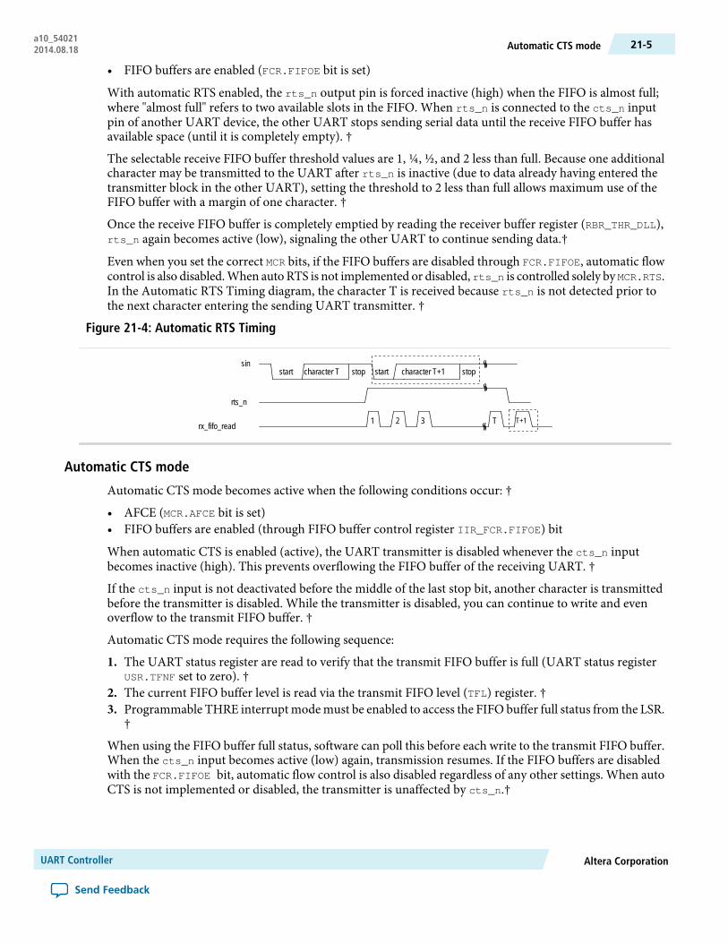
Even when you set the correct MCR bits, if the FIFO buffers are disabled through FCR.FIFOE, automatic flowcontrol is also disabled.When autoRTS is not implemented or disabled, rts_n is controlled solely by MCR.RTS.In the Automatic RTS Timing diagram, the character T is received because rts_n is not detected prior tothe next character entering the sending UART transmitter. †
Figure 21-4: Automatic RTS Timing
sin
rts_n
rx_fifo_read
start character T stop start character T+1 stop
1 2 3 T T+1
Automatic CTS mode
Automatic CTS mode becomes active when the following conditions occur: †
• AFCE (MCR.AFCE bit is set)• FIFO buffers are enabled (through FIFO buffer control register IIR_FCR.FIFOE) bit
When automatic CTS is enabled (active), the UART transmitter is disabled whenever the cts_n inputbecomes inactive (high). This prevents overflowing the FIFO buffer of the receiving UART. †
If the cts_n input is not deactivated before the middle of the last stop bit, another character is transmittedbefore the transmitter is disabled. While the transmitter is disabled, you can continue to write and evenoverflow to the transmit FIFO buffer. †
Automatic CTS mode requires the following sequence:
1. The UART status register are read to verify that the transmit FIFO buffer is full (UART status registerUSR.TFNF set to zero). †
2. The current FIFO buffer level is read via the transmit FIFO level (TFL) register. †3. Programmable THRE interrupt mode must be enabled to access the FIFO buffer full status from the LSR.
†
When using the FIFO buffer full status, software can poll this before each write to the transmit FIFO buffer.When the cts_n input becomes active (low) again, transmission resumes. If the FIFO buffers are disabledwith the FCR.FIFOE bit, automatic flow control is also disabled regardless of any other settings. When autoCTS is not implemented or disabled, the transmitter is unaffected by cts_n.†
Altera CorporationUART Controller
Send Feedback
21-5Automatic CTS modea10_540212014.08.18

Figure 21-5: Automatic CTS Timing
sout
cts_n
start data bits stopstart
Disabled
data bits stop start data bits stop
Interface Pins
Table 21-2: Interface Pins
DescriptionDirectionWidthPin
Serial InputInput1 bitRX
Serial OutputOutput1 bitTX
Clear to sendInput1 bitCTS
Request to sendOutput1 bitRTS
FPGA Routing
Table 21-3: Signals for FPGA Routing
DescriptionDirectionWidthSignal
Serial inputInput1 bituart_rxd
Serial outputOutput1 bituart_txd
Clear to sendInput1 bituart_cts
Request to sendOutput1 bituart_rts
Data set readyInput1 bituart_dsr
Data carrier detectInput1 bituart_dcd
Ring indicatorInput1 bituart_ri
Data terminal readyOutput1 bituart_dtr
User defined output 1Output1 bituart_out1_n
User defined output 2Output1 bituart_out2_n
ClocksThe UART controller is connected to the l4_sp_clk clock. The clock input is driven by the clock manager.
UART ControllerAltera Corporation
Send Feedback
a10_54021Interface Pins21-6 2014.08.18

Related InformationClock ManagerFor more information, refer to the Clock Manager chapter in the Hard Processor System Technical ReferenceManual.
ResetsThe UART controller is connected to the uart_rst_n reset signal. The reset manager drives the signal ona cold or warm reset.
Related InformationReset ManagerFor more information, refer to the Reset Manager chapter in the Hard Processor System Technical ReferenceManual.
InterruptsThe assertion of the UART interrupt output signal occurs when one of the following interrupt types areenabled and active: †
Table 21-4: Interrupt Types and Priority †
Interrupt Reset ControlSourcePriorityInterrupt Type
Reading the line statusRegister.
Overrun, parity and framing errors, breakcondition.
HighestReceiver linestatus
Reading the receiver bufferregister (FIFOs disabled)or the FIFO drops belowthe trigger level (FIFOsenabled)
Receiver data available (FIFOs disabled)or RCVR FIFO trigger level reached(FIFOs enabled).
SecondReceived dataavailable
Reading the receiver bufferRegister.
No characters in or out of the ReceiveFIFO during the last 4 character timesand there is at least 1 character in itduring this Time.
SecondCharactertimeoutindication
Reading the IIR register(if source of interrupt); or,writing into THR (FIFOs orProgrammable THREMode not enabled) orTransmit FIFO abovethreshold (FIFOs andProgrammable THREMode enabled).
Transmitter holding register empty(Programmable THRE Mode disabled)or Transmit FIFO at or below threshold(Programmable THRE Mode enabled).
ThirdTransmitholding registerempty
Reading the Modem statusRegister.
Clear to send or data set ready or ringindicator or data carrier detect. If autoflow control mode is enabled, a changein CTS (that is, DCTS set) does not causean interrupt.
FourthModem Status
Altera CorporationUART Controller
Send Feedback
21-7Resetsa10_540212014.08.18
You can enable the interrupt types with the interrupt enable register (IER_DLH).
Received Data Available" and "Character Timeout Indication" are enabled by a single bit in theIER_DLH register, because they have the same priority.
Note:
Once an interrupt is signaled, you can determine the interrupt source by reading the Interrupt IdentityRegister (IIR).
Programmable THRE Interrupt
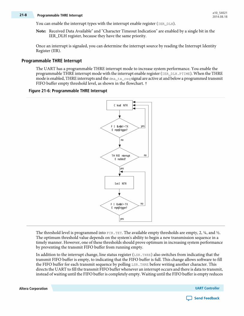
The UART has a programmable THRE interrupt mode to increase system performance. You enable theprogrammable THRE interrupt mode with the interrupt enable register (IER_DLH.PTIME). When the THREmode is enabled, THRE interrupts and the dma_tx_req signal are active at and below a programmed transmitFIFO buffer empty threshold level, as shown in the flowchart. †
Figure 21-6: Programmable THRE Interrupt
FIFO Level > TXEmpty Trigger?
THRE InterruptEnabled?
no
yes
Clear INTR
yes
no
Set INTR
yes
noFIFO Level > TXEmpty Trigger?
The threshold level is programmed into FCR.TET. The available empty thresholds are empty, 2, ¼, and ½.The optimum threshold value depends on the system's ability to begin a new transmission sequence in atimely manner. However, one of these thresholds should prove optimum in increasing system performanceby preventing the transmit FIFO buffer from running empty.
In addition to the interrupt change, line status register (LSR.THRE) also switches from indicating that thetransmit FIFO buffer is empty, to indicating that the FIFO buffer is full. This change allows software to fillthe FIFO buffer for each transmit sequence by polling LSR.THRE before writing another character. Thisdirects the UART to fill the transmit FIFO buffer whenever an interrupt occurs and there is data to transmit,instead of waiting until the FIFO buffer is completely empty. Waiting until the FIFO buffer is empty reduces
UART ControllerAltera Corporation
Send Feedback
a10_54021Programmable THRE Interrupt21-8 2014.08.18

performance whenever the system is too busy to respond immediately. You can increase system efficiencywhen this mode is enabled in combination with automatic flow control.
When not selected or disabled, THRE interrupts and LSR.THRE function normally, reflecting an empty THRor FIFO buffer.
Figure 21-7: Interrupt Generation without Programmable THRE Interrupt Mode
THREInterruptEnabled?
TX FIFOEmpty?
yes
no
Clear INTR
yes
no
Set INTR(INTR Is Asserted If
There Are No Interrupts)
TX FIFO NotEmpty?
yes
no
DMA Controller OperationThe UART controller includes a DMA controller interface to indicate when the receive FIFO buffer data isavailable or when the transmit FIFO buffer requires data. The DMA requires two channels, one for transmitand one for receive. The UART controller supports both single and burst transfers.
The FIFO buffer depth (FIFO_DEPTH) for both the RX and TX buffers in the UART controller is 128 entries.
Related InformationDMA ControllerFormore information, refer to theDMAController chapter in theHard Processor SystemTechnical ReferenceManual.
Transmit FIFO UnderflowDuringUART serial transfers, transmit FIFO requests aremade to theDMAcontroller whenever the numberof entries in the transmit FIFO is less than or equal to the decoded level of the Transmit Empty Trigger (TET)
Altera CorporationUART Controller
Send Feedback
21-9DMA Controller Operationa10_540212014.08.18

field in the FIFO Control Register (FCR), also known as the watermark level. The DMA controller respondsby writing a burst of data to the transmit FIFO buffer, of length specified as DMA burst length. †
Data should be fetched from the DMA often enough for the transmit FIFO to perform serial transferscontinuously, that is, when the FIFO begins to empty, another DMA request should be triggered. Otherwise,the FIFO will run out of data (underflow) causing a STOP to be inserted on the UART bus. To prevent thiscondition, you must set the watermark level correctly. †
Related InformationDMA ControllerFormore information, refer to theDMAController chapter in theHard Processor SystemTechnical ReferenceManual.
Transmit Watermark LevelConsider the example where the following assumption is made: †
DMA burst length = FIFO_DEPTH - decoded watermark level of IIR_FCR.TET †
Here the number of data items to be transferred in a DMA burst is equal to the empty space in the transmitFIFO. Consider the following two different watermark level settings: †
IIR_FCR.TET = 1
IIR_FCR.TET = 1 decodes to a watermark level of 16.
• Transmit FIFO watermark level = decoded watermark level of IIR_FCR.TET = 16 †• DMA burst length = FIFO_DEPTH - decoded watermark level of IIR_FCR.TET = 112 †• UART transmit FIFO_DEPTH = 128 †• Block transaction size =R** 448†
Figure 21-8: Transmit FIFO Watermark Level = 16
Data InDecoded watermarklevel of IIR_FCR.TET = 16
FIFO_DEPTH - IIR_FCR.TET = 112FIFO_DEPTH = 128
Transmit FIFOWatermark Level
Data Out
Empty
Full
TransmitFIFO Buffer
DMAController
The number of burst transactions needed equals the block size divided by the number of data items perburst:
Block transaction size/DMA burst length = 448/112 = 4
The number of burst transactions in the DMA block transfer is 4. But the watermark level, decoded level ofIIR_FCR.TET, is quite low. Therefore, the probability of transmit underflow is high where the UART serialtransmit line needs to transmit data, but there is no data left in the transmit FIFO. This occurs because theDMA has not had time to service the DMA request before the FIFO becomes empty.
UART ControllerAltera Corporation
Send Feedback
a10_54021Transmit Watermark Level21-10 2014.08.18

IIR_FCR.TET = 3
IIR_FCR.TET = 3 decodes to a watermark level of 64.
• Transmit FIFO watermark level = decoded watermark level of IIR_FCR.TET = 64 †• DMA burst length = FIFO_DEPTH - decoded watermark level of IIR_FCR.TET = 64†• UART transmit FIFO_DEPTH = 128 †• Block transaction size = 448 †
Figure 21-9: Transmit FIFO Watermark Level = 64
Decoded watermarklevel of IIR_FCR.TET = 64
FIFO_DEPTH - IIR_FCR.TET = 64FIFO_DEPTH = 128
Transmit FIFOWatermark Level
Data Out
TransmitFIFO Buffer
Empty
FullDMA
ControllerData In
Number of burst transactions in block: †
Block transaction size/DMA burst length = 448/64 = 7 †
In this block transfer, there are 15 destination burst transactions in aDMAblock transfer. But thewatermarklevel, decoded level of IIR_FCR.TET, is high. Therefore, the probability of UART transmit underflow is lowbecause the DMA controller has plenty of time to service the destination burst transaction request beforethe UART transmit FIFO becomes empty. †
Thus, the second case has a lower probability of underflow at the expense of more burst transactions perblock. This provides a potentially greater amount of bursts per block and worse bus utilization than theformer case. †
Therefore, the goal in choosing a watermark level is to minimize the number of transactions per block, whileat the same time keeping the probability of an underflow condition to an acceptable level. In practice, thisis a function of the ratio of the rate at which the UART transmits data to the rate at which the DMA canrespond to destination burst requests. †
Transmit FIFO OverflowSetting the DMA burst length to a value greater than the watermark level that triggers the DMA requestmight cause overflow when there is not enough space in the transmit FIFO to service the destination burstrequest. Therefore, the following equation must be adhered to in order to avoid overflow: †
DMA burst length <= FIFO_DEPTH - decoded watermark level of IIR_FCR.TET
In case 2: decoded watermark level of IIR_FCR.TET = 64, the amount of space in the transmit FIFO at thetime of the burst request is made is equal to the DMA burst length. Thus, the transmit FIFO may be full, butnot overflowed, at the completion of the burst transaction. †
Therefore, for optimal operation, DMA burst length must be set at the FIFO level that triggers a transmitDMA request; that is: †
DMA burst length = FIFO_DEPTH - decoded watermark level of IIR_FCR.TET
Altera CorporationUART Controller
Send Feedback
21-11IIR_FCR.TET = 3a10_540212014.08.18

Adhering to this equation reduces the number of DMA bursts needed for block transfer, and this in turnimproves bus utilization. †
The transmit FIFO will not be full at the end of a DMA burst transfer if the UART controller has successfullytransmitted one data item or more on the UART serial transmit line during the transfer. †
Receive FIFO OverflowDuring UART serial transfers, receive FIFO requests are made to the DMA whenever the number of entriesin the receive FIFO is at or above the decoded level of Receive Trigger (RT) field in the FIFO Control Register(IIR_FCR). This is known as the watermark level. The DMA responds by fetching a burst of data from thereceive FIFO. †
Data should be fetched by theDMAoften enough for the receive FIFO to accept serial transfers continuously,that is, when the FIFO begins to fill, another DMA transfer is requested. Otherwise the FIFO will fill withdata (overflow). To prevent this condition, the user must set the watermark level correctly. †
Receive Watermark LevelSimilar to choosing the transmit watermark level described earlier, the receive watermark level, decodedwatermark level of IIR_FCR.RT, should be set to minimize the probability of overflow, as shown in theReceive FIFO Buffer diagram. It is a tradeoff between the number of DMA burst transactions required perblock versus the probability of an overflow occurring. †
Receive FIFO UnderflowSetting the source transaction burst length greater than thewatermark level can cause underflowwhere thereis not enough data to service the source burst request. Therefore, the following equation must be adheredto avoid underflow: †
DMA burst length = decoded watermark level of IIR_FCR.RT + 1
If the number of data items in the receive FIFO is equal to the source burst length at the time of the burstrequest is made, the receive FIFO may be emptied, but not underflowed, at the completion of the bursttransaction. For optimal operation,DMAburst length should be set at thewatermark level, decodedwatermarklevel of IIR_FCR.RT. †
Adhering to this equation reduces the number of DMA bursts in a block transfer, which in turn can avoidunderflow and improve bus utilization. †
The receive FIFO will not be empty at the end of the source burst transaction if the UART controller hassuccessfully received one data item or more on the UART serial receive line during the burst. †
Figure 21-10: Receive FIFO Buffer
Decoded watermarklevel of IIR_FCR.RT
DMAControllerData Out
Receive FIFOWatermark Level
Data In
Empty
Full
ReceiveFIFO Buffer
UART ControllerAltera Corporation
Send Feedback
a10_54021Receive FIFO Overflow21-12 2014.08.18
Address Map and Register DefinitionsThe address map and register definitions for this module will be available in a future document revision.
Document Revision History
Table 21-5: Document Revision History
ChangesVersionDate
Initial release.2014.08.18August 2014
Altera CorporationUART Controller
Send Feedback
21-13Address Map and Register Definitionsa10_540212014.08.18