txb0104 4-bit bidirectional voltage-level translator ... · processor peripheral vcca vccb product...
TRANSCRIPT
Processor Peripheral
VCCA VCCB
Product
Folder
Order
Now
Technical
Documents
Tools &
Software
Support &Community
An IMPORTANT NOTICE at the end of this data sheet addresses availability, warranty, changes, use in safety-critical applications,intellectual property matters and other important disclaimers. PRODUCTION DATA.
TXB0104SCES650I –APRIL 2006–REVISED MARCH 2018
TXB0104 4-Bit Bidirectional Voltage-level Translator With Automatic Direction Sensingand ±15-kV ESD Protection
1
1 Features1• 1.2-V to 3.6-V on A Port and 1.65-V to 5.5-V
on B Port (VCCA ≤ VCCB)• VCC Isolation Feature: If Either VCC Input Is at
GND, All Outputs Are in the High-ImpedanceState
• Output Enable (OE) Input Circuit Referenced toVCCA
• Low Power Consumption, 5-μA Maximum ICC
• I OFF Supports Partial Power-Down ModeOperation
• Latch-Up Performance Exceeds 100 mA PerJESD 78, Class II
• ESD Protection Exceeds JESD 22– A Port:
– 2500-V Human-Body Model (A114-B)– 1500-V Charged-Device Model (C101)
– B Port:– ±15-kV Human-Body Model (A114-B)– 1500-V Charged-Device Model (C101)
2 Applications• Headsets• Smartphones• Tablets• Desktop PC
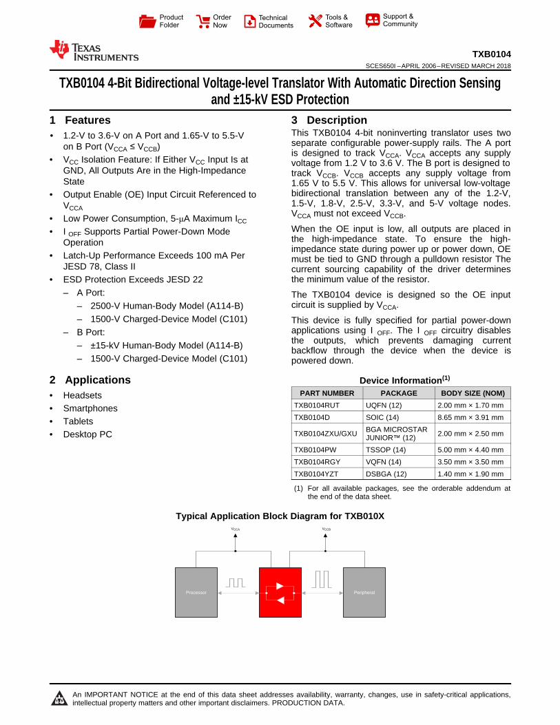
3 DescriptionThis TXB0104 4-bit noninverting translator uses twoseparate configurable power-supply rails. The A portis designed to track VCCA. VCCA accepts any supplyvoltage from 1.2 V to 3.6 V. The B port is designed totrack VCCB. VCCB accepts any supply voltage from1.65 V to 5.5 V. This allows for universal low-voltagebidirectional translation between any of the 1.2-V,1.5-V, 1.8-V, 2.5-V, 3.3-V, and 5-V voltage nodes.VCCA must not exceed VCCB.
When the OE input is low, all outputs are placed inthe high-impedance state. To ensure the high-impedance state during power up or power down, OEmust be tied to GND through a pulldown resistor Thecurrent sourcing capability of the driver determinesthe minimum value of the resistor.
The TXB0104 device is designed so the OE inputcircuit is supplied by VCCA.
This device is fully specified for partial power-downapplications using I OFF. The I OFF circuitry disablesthe outputs, which prevents damaging currentbackflow through the device when the device ispowered down.
Device Information(1)
PART NUMBER PACKAGE BODY SIZE (NOM)TXB0104RUT UQFN (12) 2.00 mm × 1.70 mmTXB0104D SOIC (14) 8.65 mm × 3.91 mm
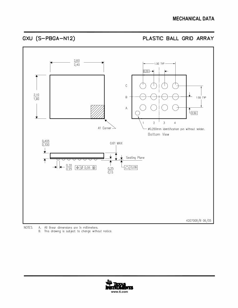
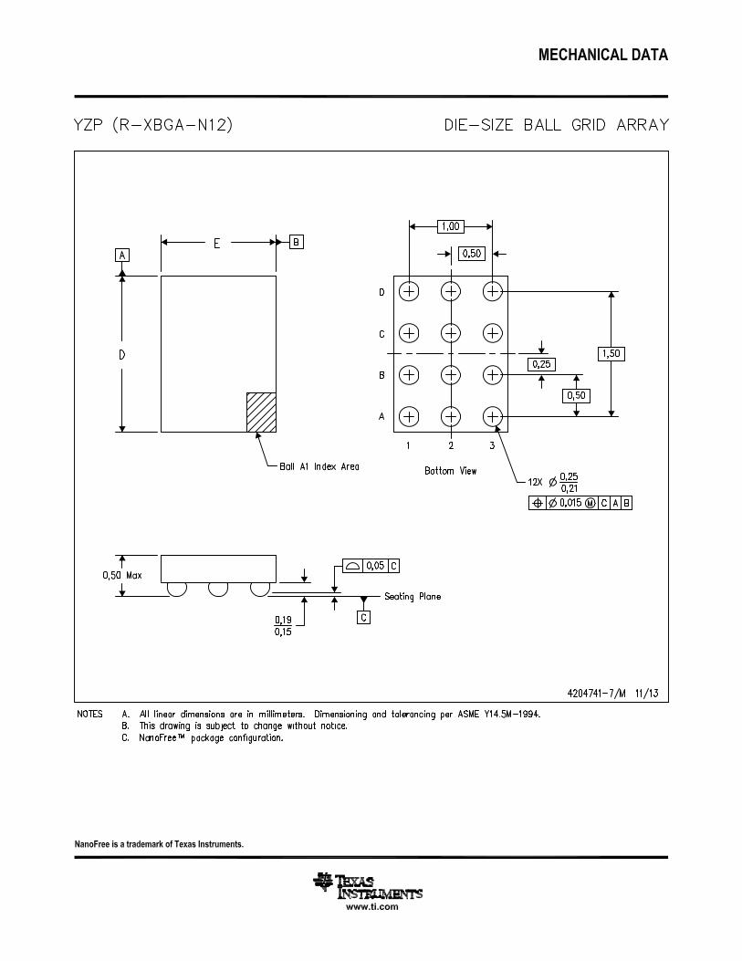
TXB0104ZXU/GXU BGA MICROSTARJUNIOR™ (12) 2.00 mm × 2.50 mm
TXB0104PW TSSOP (14) 5.00 mm × 4.40 mmTXB0104RGY VQFN (14) 3.50 mm × 3.50 mmTXB0104YZT DSBGA (12) 1.40 mm × 1.90 mm
(1) For all available packages, see the orderable addendum atthe end of the data sheet.
Typical Application Block Diagram for TXB010X
2
TXB0104SCES650I –APRIL 2006–REVISED MARCH 2018 www.ti.com
Product Folder Links: TXB0104
Submit Documentation Feedback Copyright © 2006–2018, Texas Instruments Incorporated
Table of Contents1 Features .................................................................. 12 Applications ........................................................... 13 Description ............................................................. 14 Revision History..................................................... 25 Pin Configuration and Functions ......................... 36 Specifications......................................................... 5
6.1 Absolute Maximum Ratings ..................................... 56.2 ESD Ratings ............................................................ 56.3 Recommended Operating Conditions....................... 66.4 Thermal Information .................................................. 66.5 Electrical Characteristics .......................................... 76.6 Timing Requirements: VCCA = 1.2 V ......................... 86.7 Timing Requirements: VCCA = 1.5 V ± 0.1 V ............ 86.8 Timing Requirements: VCCA = 1.8 V ± 0.15 V .......... 86.9 Timing Requirements: VCCA = 2.5 V ± 0.2 V ............ 86.10 Timing Requirements: VCCA = 3.3 V ± 0.3 V .......... 86.11 Switching Characteristics: VCCA = 1.2 V ................. 96.12 Switching Characteristics: VCCA = 1.5 V ± 0.1 V .... 96.13 Switching Characteristics: VCCA = 1.8 V ± 0.15 V 106.14 Switching Characteristics: VCCA = 2.5 V ± 0.2 V .. 106.15 Switching Characteristics: VCCA = 3.3 V ± 0.3 V .. 116.16 Operating Characteristics: VCCA = 1.2 V to 1.5 V,
VCCB = 1.5 V to 1.8 V............................................... 126.17 Operating Characteristics: VCCA = 1.8 V to 3.3 V,
VCCB = 1.8 V to 5 V.................................................. 126.18 Typical Characteristics .......................................... 13
7 Parameter Measurement Information ................ 148 Detailed Description ............................................ 16
8.1 Overview ................................................................. 168.2 Functional Block Diagram ....................................... 168.3 Feature Description................................................. 178.4 Device Functional Modes........................................ 19
9 Application and Implementation ........................ 209.1 Application Information............................................ 209.2 Typical Application ................................................. 20
10 Power Supply Recommendations ..................... 2211 Layout................................................................... 22
11.1 Layout Guidelines ................................................. 2211.2 Layout Example .................................................... 22
12 Device and Documentation Support ................. 2312.1 Receiving Notification of Documentation Updates 2312.2 Community Resources.......................................... 2312.3 Trademarks ........................................................... 2312.4 Electrostatic Discharge Caution............................ 2312.5 Glossary ................................................................ 23
13 Mechanical, Packaging, and OrderableInformation ........................................................... 24
4 Revision HistoryNOTE: Page numbers for previous revisions may differ from page numbers in the current version.
Changes from Revision H (Janurary 2018) to Revision I Page
• Updated Pin Functions table ................................................................................................................................................. 4• Added Pin Assignments table for GXU and ZXU package ................................................................................................... 4• Added Pin Assignments table for YZT package .................................................................................................................... 4• Updated Layout Example ..................................................................................................................................................... 22
Changes from Revision G (November 2014) to Revision H Page
• Added package families to package pinout drawings in Pin Configuration and Functions section ...................................... 3• Added junction temperature range in Absolute Maximum Ratingstable................................................................................. 5• Changed unit from V to kV in ESD Ratings table................................................................................................................... 5
Changes from Revision F (May 2012) to Revision G Page
• Added Pin Configuration and Functions section, Handling Rating table, Feature Description section, DeviceFunctional Modes, Application and Implementation section, Power Supply Recommendations section, Layoutsection, Device and Documentation Support section, and Mechanical, Packaging, and Orderable Informationsection ................................................................................................................................................................................... 1
14
13
12
11
10
9
8
1
2
3
4
5
6
7 OEGND
NC
A4
A3
A2
VCCA
NC
B4
B3
B2
B1
VCCB
A1
VCCB
B1
B2
B3
3
2
6
10
1
4 8
9
1112
A2
A3
VCCA
A1
OE
GN
DB45 7A4
PLACEHOLDER
D
C
B
A
3 2 1
ExposedCenter
Pad
1 14
7 8
2
3
4
5
6
13
12
11
10
9
B1
B2
B3
B4
NC
A1
A2
A3
A4
NC
OE
VC
CB
GN
DV
CC
A
4
3
2
1
A B C
3
TXB0104www.ti.com SCES650I –APRIL 2006–REVISED MARCH 2018
Product Folder Links: TXB0104
Submit Documentation FeedbackCopyright © 2006–2018, Texas Instruments Incorporated
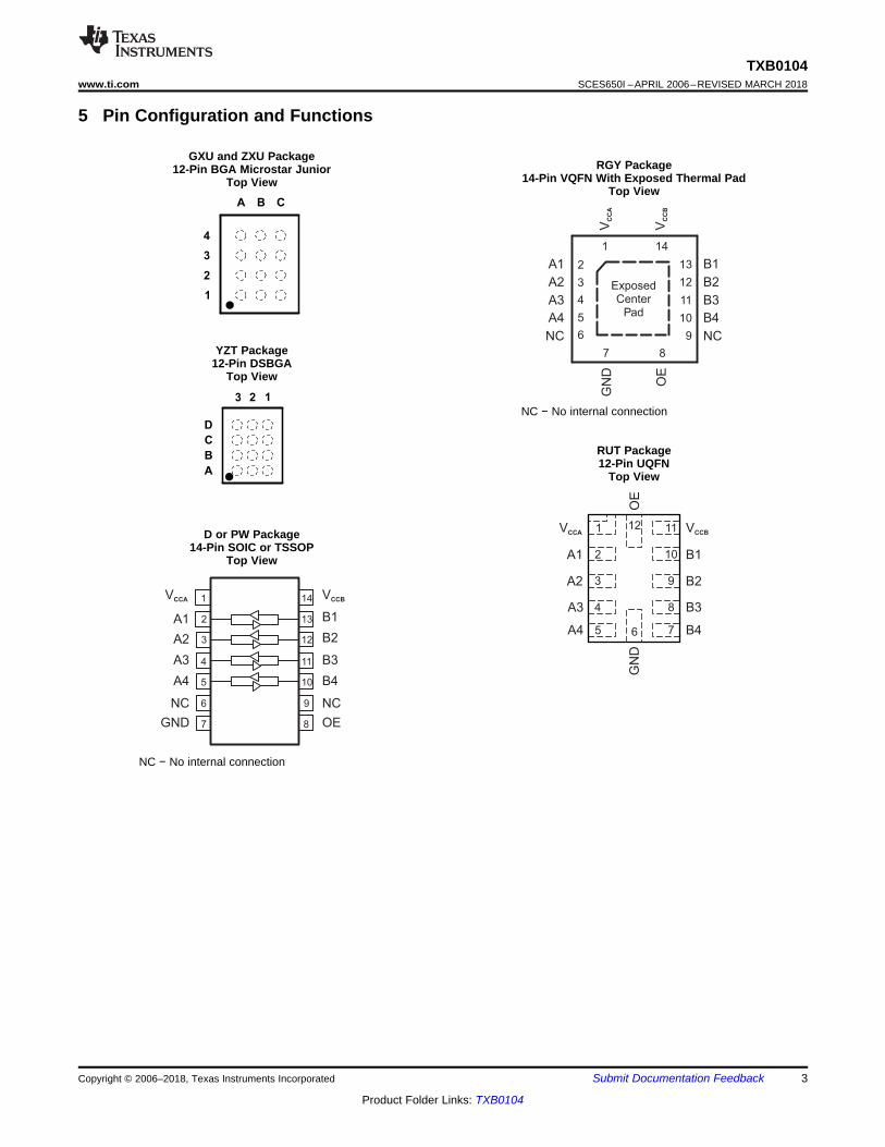
5 Pin Configuration and Functions
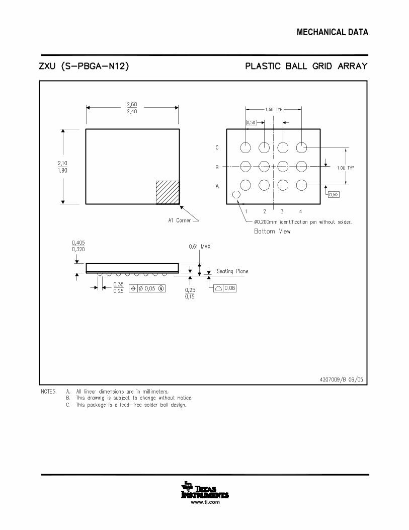
GXU and ZXU Package12-Pin BGA Microstar Junior
Top View
YZT Package12-Pin DSBGA
Top View
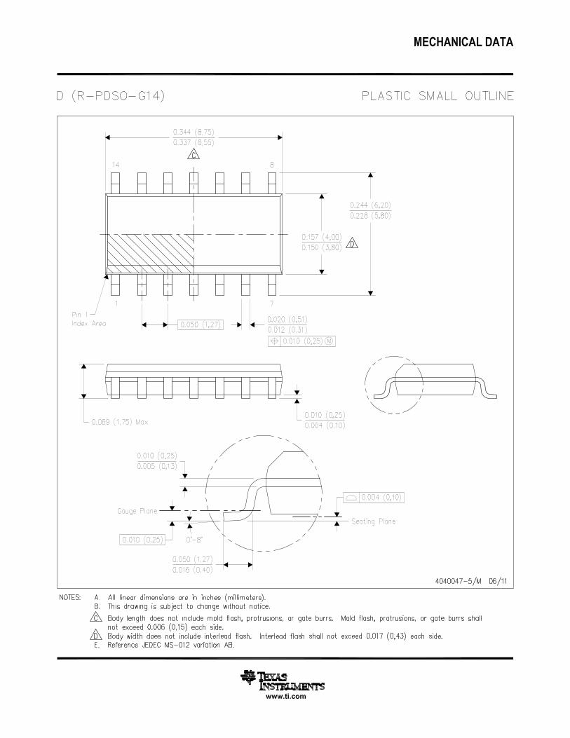
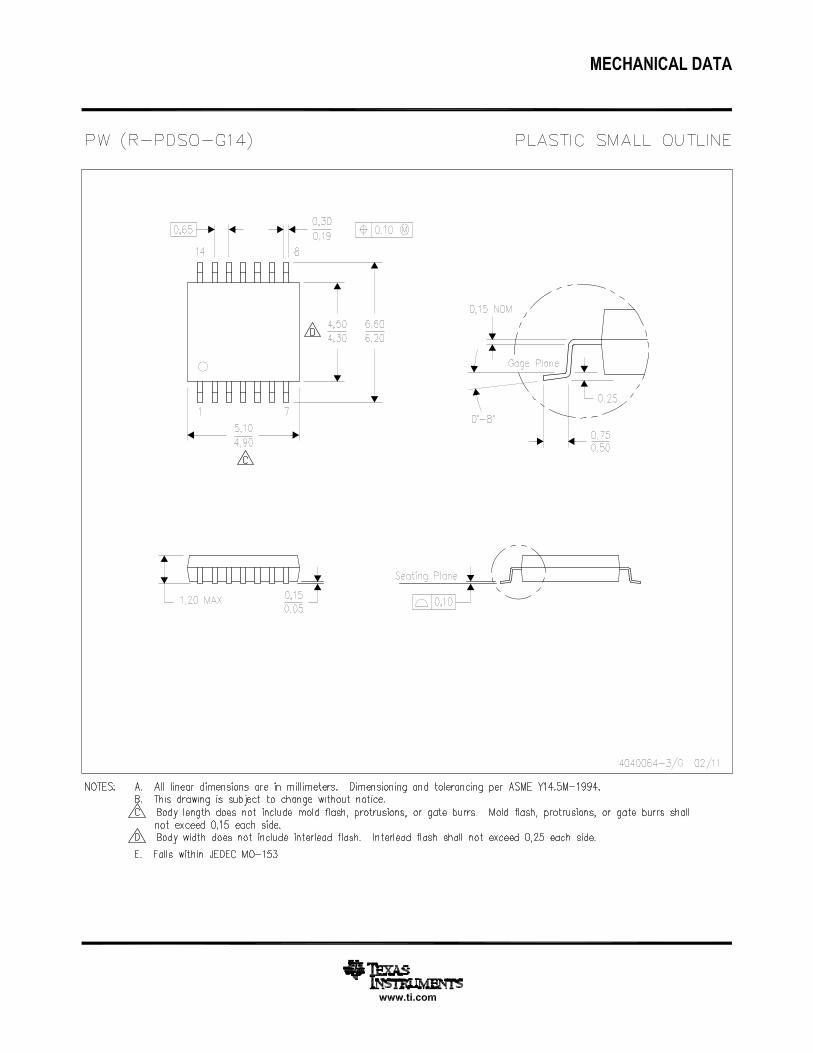
D or PW Package14-Pin SOIC or TSSOP
Top View
NC − No internal connection
RGY Package14-Pin VQFN With Exposed Thermal Pad
Top View
NC − No internal connection
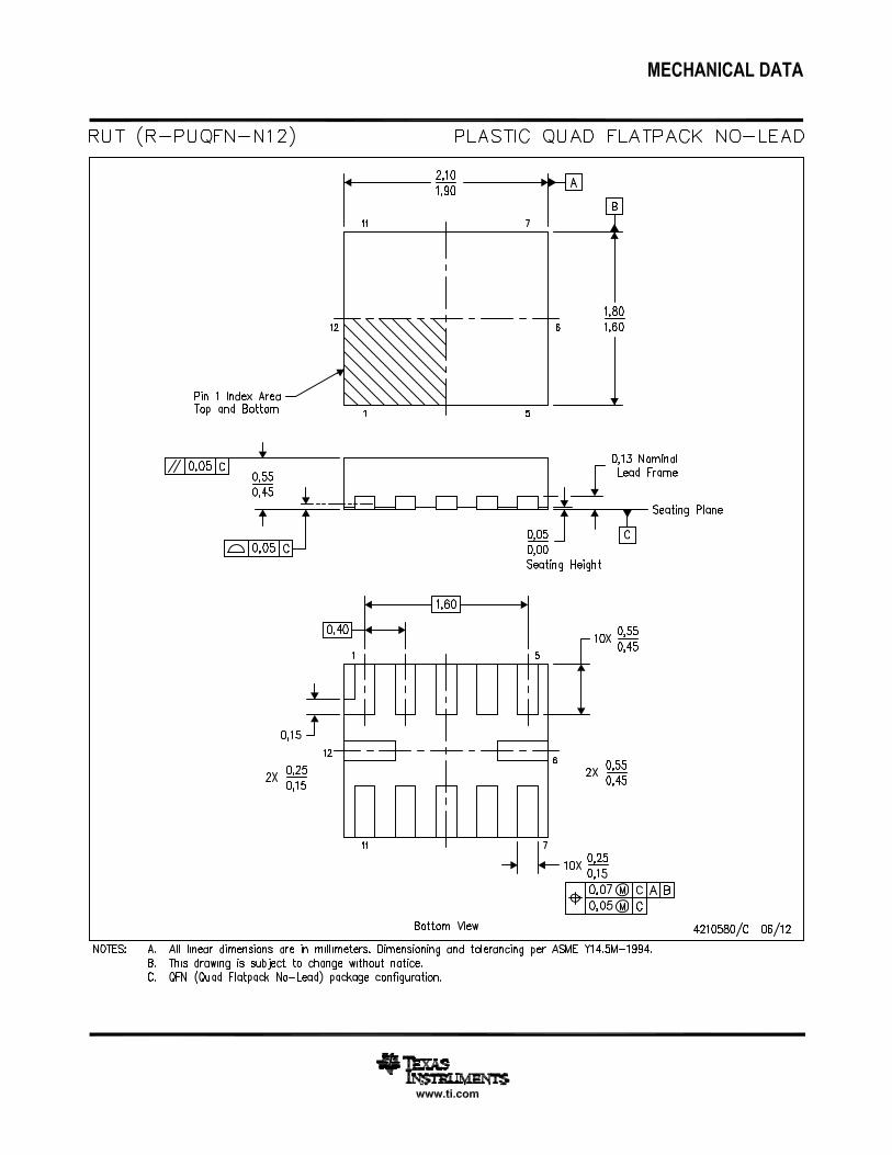
RUT Package12-Pin UQFN
Top View
4
TXB0104SCES650I –APRIL 2006–REVISED MARCH 2018 www.ti.com
Product Folder Links: TXB0104
Submit Documentation Feedback Copyright © 2006–2018, Texas Instruments Incorporated
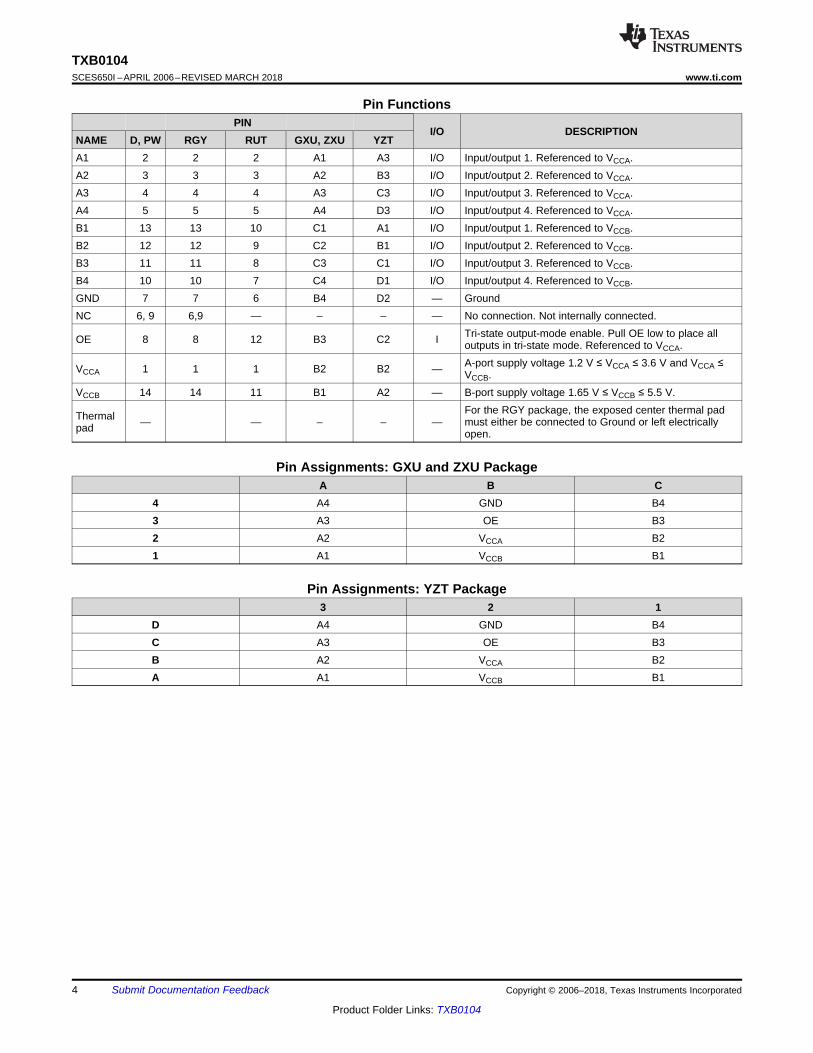
Pin FunctionsPIN
I/O DESCRIPTIONNAME D, PW RGY RUT GXU, ZXU YZTA1 2 2 2 A1 A3 I/O Input/output 1. Referenced to VCCA.A2 3 3 3 A2 B3 I/O Input/output 2. Referenced to VCCA.A3 4 4 4 A3 C3 I/O Input/output 3. Referenced to VCCA.A4 5 5 5 A4 D3 I/O Input/output 4. Referenced to VCCA.B1 13 13 10 C1 A1 I/O Input/output 1. Referenced to VCCB.B2 12 12 9 C2 B1 I/O Input/output 2. Referenced to VCCB.B3 11 11 8 C3 C1 I/O Input/output 3. Referenced to VCCB.B4 10 10 7 C4 D1 I/O Input/output 4. Referenced to VCCB.GND 7 7 6 B4 D2 — GroundNC 6, 9 6,9 — – – — No connection. Not internally connected.
OE 8 8 12 B3 C2 I Tri-state output-mode enable. Pull OE low to place alloutputs in tri-state mode. Referenced to VCCA.
VCCA 1 1 1 B2 B2 — A-port supply voltage 1.2 V ≤ VCCA ≤ 3.6 V and VCCA ≤VCCB.
VCCB 14 14 11 B1 A2 — B-port supply voltage 1.65 V ≤ VCCB ≤ 5.5 V.
Thermalpad — — – – —
For the RGY package, the exposed center thermal padmust either be connected to Ground or left electricallyopen.
Pin Assignments: GXU and ZXU PackageA B C
4 A4 GND B43 A3 OE B32 A2 VCCA B21 A1 VCCB B1
Pin Assignments: YZT Package3 2 1
D A4 GND B4C A3 OE B3B A2 VCCA B2A A1 VCCB B1
5
TXB0104www.ti.com SCES650I –APRIL 2006–REVISED MARCH 2018
Product Folder Links: TXB0104
Submit Documentation FeedbackCopyright © 2006–2018, Texas Instruments Incorporated
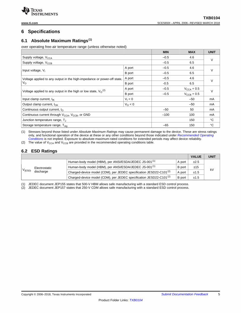
(1) Stresses beyond those listed under Absolute Maximum Ratings may cause permanent damage to the device. These are stress ratingsonly, and functional operation of the device at these or any other conditions beyond those indicated under Recommended OperatingConditions is not implied. Exposure to absolute-maximum-rated conditions for extended periods may affect device reliability.
(2) The value of VCCA and VCCB are provided in the recommended operating conditions table.
6 Specifications
6.1 Absolute Maximum Ratings (1)
over operating free-air temperature range (unless otherwise noted)MIN MAX UNIT
Supply voltage, VCCA –0.5 4.6V
Supply voltage, VCCB –0.5 6.5
Input voltage, VIA port –0.5 4.6
VB port –0.5 6.5
Voltage applied to any output in the high-impedance or power-off state,VO
A port –0.5 4.6V
B port -0.5 6.5
Voltage applied to any output in the high or low state, VO(2) A port –0.5 VCCA + 0.5
VB port –0.5 VCCB + 0.5
Input clamp current, IIK VI < 0 –50 mAOutput clamp current, IOK VO < 0 –50 mAContinuous output current, IO –50 50 mAContinuous current through VCCA, VCCB, or GND –100 100 mAJunction temperature range, TJ 150 °CStorage temperature range, Tstg –65 150 °C
(1) JEDEC document JEP155 states that 500-V HBM allows safe manufacturing with a standard ESD control process.(2) JEDEC document JEP157 states that 250-V CDM allows safe manufacturing with a standard ESD control process.
6.2 ESD RatingsVALUE UNIT
V(ESD)Electrostaticdischarge
Human-body model (HBM), per ANSI/ESDA/JEDEC JS-001 (1) A port ±2.5
kVHuman-body model (HBM), per ANSI/ESDA/JEDEC JS-001 (1) B port ±15Charged-device model (CDM), per JEDEC specification JESD22-C101 (2) A port ±1.5Charged-device model (CDM), per JEDEC specification JESD22-C101 (2) B port ±1.5
6
TXB0104SCES650I –APRIL 2006–REVISED MARCH 2018 www.ti.com
Product Folder Links: TXB0104
Submit Documentation Feedback Copyright © 2006–2018, Texas Instruments Incorporated
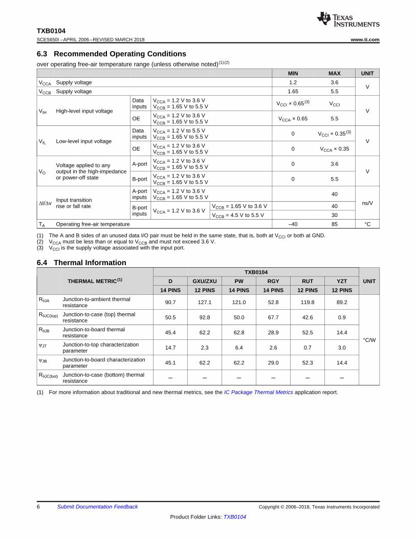
(1) The A and B sides of an unused data I/O pair must be held in the same state, that is, both at VCCI or both at GND.(2) VCCA must be less than or equal to VCCB and must not exceed 3.6 V.(3) VCCI is the supply voltage associated with the input port.
6.3 Recommended Operating Conditionsover operating free-air temperature range (unless otherwise noted) (1) (2)
MIN MAX UNITVCCA Supply voltage 1.2 3.6
VVCCB Supply voltage 1.65 5.5
VIH High-level input voltage
Datainputs
VCCA = 1.2 V to 3.6 VVCCB = 1.65 V to 5.5 V VCCI × 0.65 (3) VCCI
VOE VCCA = 1.2 V to 3.6 V
VCCB = 1.65 V to 5.5 V VCCA × 0.65 5.5
VIL Low-level input voltage
Datainputs
VCCA = 1.2 V to 5.5 VVCCB = 1.65 V to 5.5 V 0 VCCI × 0.35 (3)
VOE VCCA = 1.2 V to 3.6 V
VCCB = 1.65 V to 5.5 V 0 VCCA × 0.35
VO
Voltage applied to anyoutput in the high-impedanceor power-off state
A-port VCCA = 1.2 V to 3.6 VVCCB = 1.65 V to 5.5 V 0 3.6
VB-port VCCA = 1.2 V to 3.6 V
VCCB = 1.65 V to 5.5 V 0 5.5
Δt/Δv Input transitionrise or fall rate
A-portinputs
VCCA = 1.2 V to 3.6 VVCCB = 1.65 V to 5.5 V 40
ns/VB-portinputs VCCA = 1.2 V to 3.6 V
VCCB = 1.65 V to 3.6 V 40VCCB = 4.5 V to 5.5 V 30
TA Operating free-air temperature –40 85 °C
(1) For more information about traditional and new thermal metrics, see the IC Package Thermal Metrics application report.
6.4 Thermal Information
THERMAL METRIC (1)TXB0104
UNITD GXU/ZXU PW RGY RUT YZT14 PINS 12 PINS 14 PINS 14 PINS 12 PINS 12 PINS
RθJA Junction-to-ambient thermalresistance 90.7 127.1 121.0 52.8 119.8 89.2
°C/W
RθJC(top) Junction-to-case (top) thermalresistance 50.5 92.8 50.0 67.7 42.6 0.9
RθJB Junction-to-board thermalresistance 45.4 62.2 62.8 28.9 52.5 14.4
ψJT Junction-to-top characterizationparameter 14.7 2.3 6.4 2.6 0.7 3.0
ψJB Junction-to-board characterizationparameter 45.1 62.2 62.2 29.0 52.3 14.4
RθJC(bot) Junction-to-case (bottom) thermalresistance
7
TXB0104www.ti.com SCES650I –APRIL 2006–REVISED MARCH 2018
Product Folder Links: TXB0104
Submit Documentation FeedbackCopyright © 2006–2018, Texas Instruments Incorporated
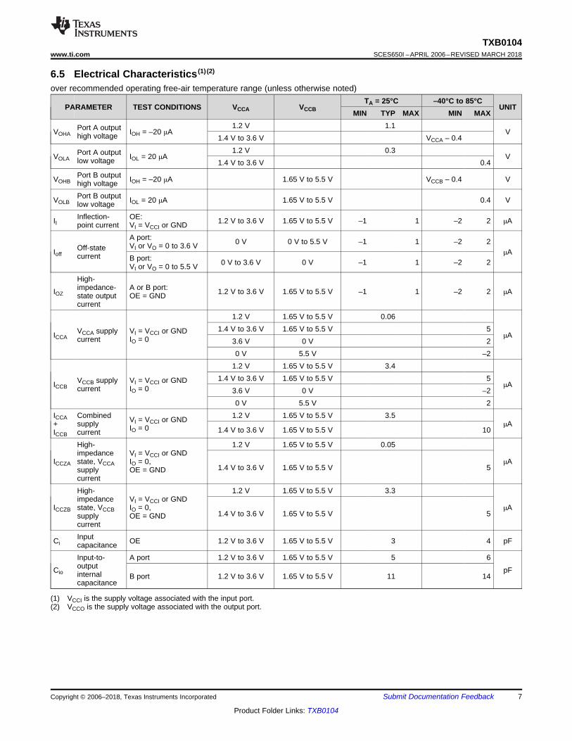
(1) VCCI is the supply voltage associated with the input port.(2) VCCO is the supply voltage associated with the output port.
6.5 Electrical Characteristics (1) (2)
over recommended operating free-air temperature range (unless otherwise noted)
PARAMETER TEST CONDITIONS VCCA VCCBTA = 25°C –40°C to 85°C
UNITMIN TYP MAX MIN MAX
VOHAPort A outputhigh voltage IOH = –20 μA
1.2 V 1.1V
1.4 V to 3.6 V VCCA – 0.4
VOLAPort A outputlow voltage IOL = 20 μA
1.2 V 0.3V
1.4 V to 3.6 V 0.4
VOHBPort B outputhigh voltage IOH = –20 μA 1.65 V to 5.5 V VCCB – 0.4 V
VOLBPort B outputlow voltage IOL = 20 μA 1.65 V to 5.5 V 0.4 V
IIInflection-point current
OE:VI = VCCI or GND 1.2 V to 3.6 V 1.65 V to 5.5 V –1 1 –2 2 μA
IoffOff-statecurrent
A port:VI or VO = 0 to 3.6 V 0 V 0 V to 5.5 V –1 1 –2 2
μAB port:VI or VO = 0 to 5.5 V 0 V to 3.6 V 0 V –1 1 –2 2
IOZ
High-impedance-state outputcurrent
A or B port:OE = GND 1.2 V to 3.6 V 1.65 V to 5.5 V –1 1 –2 2 μA
ICCAVCCA supplycurrent
VI = VCCI or GNDIO = 0
1.2 V 1.65 V to 5.5 V 0.06
μA1.4 V to 3.6 V 1.65 V to 5.5 V 5
3.6 V 0 V 20 V 5.5 V –2
ICCBVCCB supplycurrent
VI = VCCI or GNDIO = 0
1.2 V 1.65 V to 5.5 V 3.4
μA1.4 V to 3.6 V 1.65 V to 5.5 V 5
3.6 V 0 V –20 V 5.5 V 2
ICCA+ICCB
Combinedsupplycurrent
VI = VCCI or GNDIO = 0
1.2 V 1.65 V to 5.5 V 3.5μA
1.4 V to 3.6 V 1.65 V to 5.5 V 10
ICCZA
High-impedancestate, VCCAsupplycurrent
VI = VCCI or GNDIO = 0,OE = GND
1.2 V 1.65 V to 5.5 V 0.05
μA1.4 V to 3.6 V 1.65 V to 5.5 V 5
ICCZB
High-impedancestate, VCCBsupplycurrent
VI = VCCI or GNDIO = 0,OE = GND
1.2 V 1.65 V to 5.5 V 3.3
μA1.4 V to 3.6 V 1.65 V to 5.5 V 5
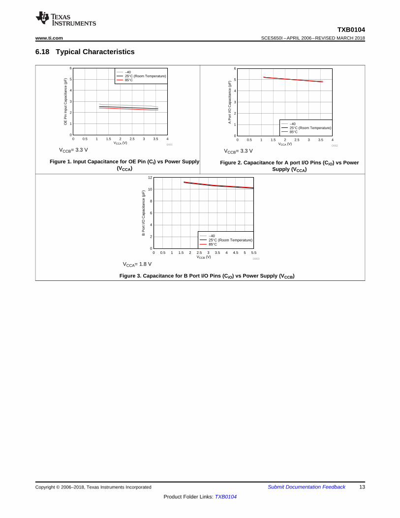
CiInputcapacitance OE 1.2 V to 3.6 V 1.65 V to 5.5 V 3 4 pF
Cio
Input-to-outputinternalcapacitance
A port 1.2 V to 3.6 V 1.65 V to 5.5 V 5 6
pFB port 1.2 V to 3.6 V 1.65 V to 5.5 V 11 14
8
TXB0104SCES650I –APRIL 2006–REVISED MARCH 2018 www.ti.com
Product Folder Links: TXB0104
Submit Documentation Feedback Copyright © 2006–2018, Texas Instruments Incorporated
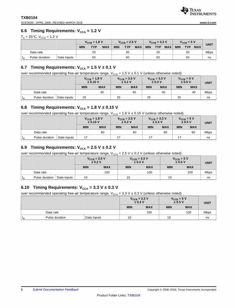
6.6 Timing Requirements: VCCA = 1.2 VTA = 25°C, VCCA = 1.2 V
VCCB = 1.8 V VCCB = 2.5 V VCCB = 3.3 V VCCB = 5 VUNIT
MIN TYP MAX MIN TYP MAX MIN TYP MAX MIN TYP MAXData rate 20 20 20 20 Mbps
tw Pulse duration Data inputs 50 50 50 50 ns
6.7 Timing Requirements: VCCA = 1.5 V ± 0.1 Vover recommended operating free-air temperature range, VCCA = 1.5 V ± 0.1 V (unless otherwise noted)
VCCB = 1.8 V± 0.15 V
VCCB = 2.5 V± 0.2 V
VCCB = 3.3 V± 0.3 V
VCCB = 5 V± 0.5 V UNIT
MIN MAX MIN MAX MIN MAX MIN MAXData rate 40 40 40 40 Mbps
tw Pulse duration Data inputs 25 25 25 25 ns
6.8 Timing Requirements: VCCA = 1.8 V ± 0.15 Vover recommended operating free-air temperature range, VCCA = 1.8 V ± 0.15 V (unless otherwise noted)
VCCB = 1.8 V± 0.15 V
VCCB = 2.5 V± 0.2 V
VCCB = 3.3 V± 0.3 V
VCCB = 5 V± 0.5 V UNIT
MIN MAX MIN MAX MIN MAX MIN MAXData rate 60 60 60 60 Mbps
tw Pulse duration Data inputs 17 17 17 17 ns
6.9 Timing Requirements: VCCA = 2.5 V ± 0.2 Vover recommended operating free-air temperature range, VCCA = 2.5 V ± 0.2 V (unless otherwise noted)
VCCB = 2.5 V± 0.2 V
VCCB = 3.3 V± 0.3 V
VCCB = 5 V± 0.5 V UNIT
MIN MAX MIN MAX MIN MAXData rate 100 100 100 Mbps
tw Pulse duration Data inputs 10 10 10 ns
6.10 Timing Requirements: VCCA = 3.3 V ± 0.3 Vover recommended operating free-air temperature range, VCCA = 3.3 V ± 0.3 V (unless otherwise noted)
VCCB = 3.3 V± 0.3 V
VCCB = 5 V± 0.5 V UNIT
MIN MAX MIN MAXData rate 100 100 Mbps
tw Pulse duration Data inputs 10 10 ns
9
TXB0104www.ti.com SCES650I –APRIL 2006–REVISED MARCH 2018
Product Folder Links: TXB0104
Submit Documentation FeedbackCopyright © 2006–2018, Texas Instruments Incorporated
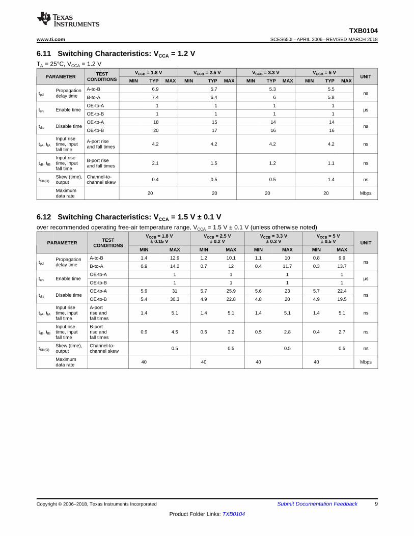
6.11 Switching Characteristics: VCCA = 1.2 VTA = 25°C, VCCA = 1.2 V
PARAMETER TESTCONDITIONS
VCCB = 1.8 V VCCB = 2.5 V VCCB = 3.3 V VCCB = 5 VUNIT
MIN TYP MAX MIN TYP MAX MIN TYP MAX MIN TYP MAX
tpdPropagationdelay time
A-to-B 6.9 5.7 5.3 5.5ns
B-to-A 7.4 6.4 6 5.8
ten Enable timeOE-to-A 1 1 1 1
µsOE-to-B 1 1 1 1
tdis Disable timeOE-to-A 18 15 14 14
nsOE-to-B 20 17 16 16
trA, tfAInput risetime, inputfall time
A-port riseand fall times 4.2 4.2 4.2 4.2 ns
trB, tfBInput risetime, inputfall time
B-port riseand fall times 2.1 1.5 1.2 1.1 ns
tSK(O)Skew (time),output
Channel-to-channel skew 0.4 0.5 0.5 1.4 ns
Maximumdata rate 20 20 20 20 Mbps
6.12 Switching Characteristics: VCCA = 1.5 V ± 0.1 Vover recommended operating free-air temperature range, VCCA = 1.5 V ± 0.1 V (unless otherwise noted)
PARAMETER TESTCONDITIONS
VCCB = 1.8 V± 0.15 V
VCCB = 2.5 V± 0.2 V
VCCB = 3.3 V± 0.3 V
VCCB = 5 V± 0.5 V UNIT
MIN MAX MIN MAX MIN MAX MIN MAX
tpdPropagationdelay time
A-to-B 1.4 12.9 1.2 10.1 1.1 10 0.8 9.9ns
B-to-A 0.9 14.2 0.7 12 0.4 11.7 0.3 13.7
ten Enable timeOE-to-A 1 1 1 1
µsOE-to-B 1 1 1 1
tdis Disable timeOE-to-A 5.9 31 5.7 25.9 5.6 23 5.7 22.4
nsOE-to-B 5.4 30.3 4.9 22.8 4.8 20 4.9 19.5
trA, tfAInput risetime, inputfall time
A-portrise andfall times
1.4 5.1 1.4 5.1 1.4 5.1 1.4 5.1 ns
trB, tfBInput risetime, inputfall time
B-portrise andfall times
0.9 4.5 0.6 3.2 0.5 2.8 0.4 2.7 ns
tSK(O)Skew (time),output
Channel-to-channel skew 0.5 0.5 0.5 0.5 ns
Maximumdata rate 40 40 40 40 Mbps
10
TXB0104SCES650I –APRIL 2006–REVISED MARCH 2018 www.ti.com
Product Folder Links: TXB0104
Submit Documentation Feedback Copyright © 2006–2018, Texas Instruments Incorporated
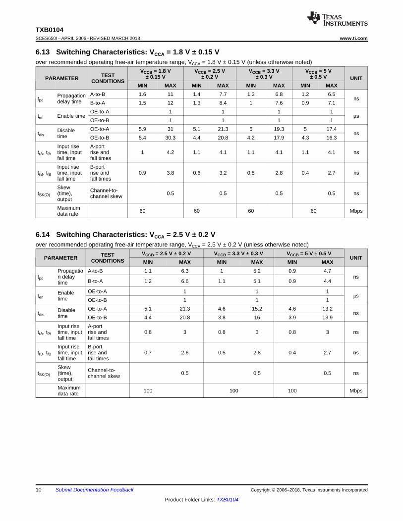
6.13 Switching Characteristics: VCCA = 1.8 V ± 0.15 Vover recommended operating free-air temperature range, VCCA = 1.8 V ± 0.15 V (unless otherwise noted)
PARAMETER TESTCONDITIONS
VCCB = 1.8 V± 0.15 V
VCCB = 2.5 V± 0.2 V
VCCB = 3.3 V± 0.3 V
VCCB = 5 V± 0.5 V UNIT
MIN MAX MIN MAX MIN MAX MIN MAX
tpdPropagationdelay time
A-to-B 1.6 11 1.4 7.7 1.3 6.8 1.2 6.5ns
B-to-A 1.5 12 1.3 8.4 1 7.6 0.9 7.1
ten Enable timeOE-to-A 1 1 1 1
µsOE-to-B 1 1 1 1
tdisDisabletime
OE-to-A 5.9 31 5.1 21.3 5 19.3 5 17.4ns
OE-to-B 5.4 30.3 4.4 20.8 4.2 17.9 4.3 16.3
trA, tfAInput risetime, inputfall time
A-portrise andfall times
1 4.2 1.1 4.1 1.1 4.1 1.1 4.1 ns
trB, tfBInput risetime, inputfall time
B-portrise andfall times
0.9 3.8 0.6 3.2 0.5 2.8 0.4 2.7 ns
tSK(O)
Skew(time),output
Channel-to-channel skew 0.5 0.5 0.5 0.5 ns
Maximumdata rate 60 60 60 60 Mbps
6.14 Switching Characteristics: VCCA = 2.5 V ± 0.2 Vover recommended operating free-air temperature range, VCCA = 2.5 V ± 0.2 V (unless otherwise noted)
PARAMETER TESTCONDITIONS
VCCB = 2.5 V ± 0.2 V VCCB = 3.3 V ± 0.3 V VCCB = 5 V ± 0.5 VUNIT
MIN MAX MIN MAX MIN MAX
tpd
Propagation delaytime
A-to-B 1.1 6.3 1 5.2 0.9 4.7ns
B-to-A 1.2 6.6 1.1 5.1 0.9 4.4
tenEnabletime
OE-to-A 1 1 1μs
OE-to-B 1 1 1
tdisDisabletime
OE-to-A 5.1 21.3 4.6 15.2 4.6 13.2ns
OE-to-B 4.4 20.8 3.8 16 3.9 13.9
trA, tfAInput risetime, inputfall time
A-portrise andfall times
0.8 3 0.8 3 0.8 3 ns
trB, tfBInput risetime, inputfall time
B-portrise andfall times
0.7 2.6 0.5 2.8 0.4 2.7 ns
tSK(O)
Skew(time),output
Channel-to-channel skew 0.5 0.5 0.5 ns
Maximumdata rate 100 100 100 Mbps
11
TXB0104www.ti.com SCES650I –APRIL 2006–REVISED MARCH 2018
Product Folder Links: TXB0104
Submit Documentation FeedbackCopyright © 2006–2018, Texas Instruments Incorporated
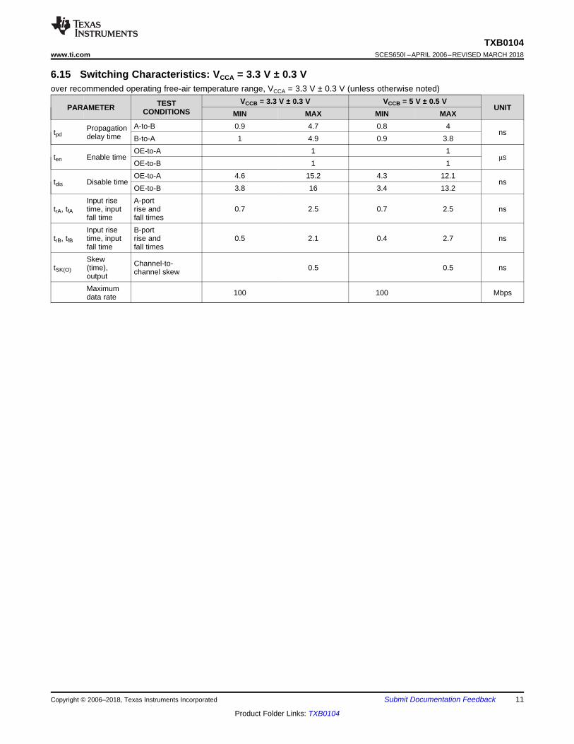
6.15 Switching Characteristics: VCCA = 3.3 V ± 0.3 Vover recommended operating free-air temperature range, VCCA = 3.3 V ± 0.3 V (unless otherwise noted)
PARAMETER TESTCONDITIONS
VCCB = 3.3 V ± 0.3 V VCCB = 5 V ± 0.5 VUNIT
MIN MAX MIN MAX
tpdPropagationdelay time
A-to-B 0.9 4.7 0.8 4ns
B-to-A 1 4.9 0.9 3.8
ten Enable timeOE-to-A 1 1
μsOE-to-B 1 1
tdis Disable timeOE-to-A 4.6 15.2 4.3 12.1
nsOE-to-B 3.8 16 3.4 13.2
trA, tfAInput risetime, inputfall time
A-portrise andfall times
0.7 2.5 0.7 2.5 ns
trB, tfBInput risetime, inputfall time
B-portrise andfall times
0.5 2.1 0.4 2.7 ns
tSK(O)
Skew(time),output
Channel-to-channel skew 0.5 0.5 ns
Maximumdata rate 100 100 Mbps
12
TXB0104SCES650I –APRIL 2006–REVISED MARCH 2018 www.ti.com
Product Folder Links: TXB0104
Submit Documentation Feedback Copyright © 2006–2018, Texas Instruments Incorporated
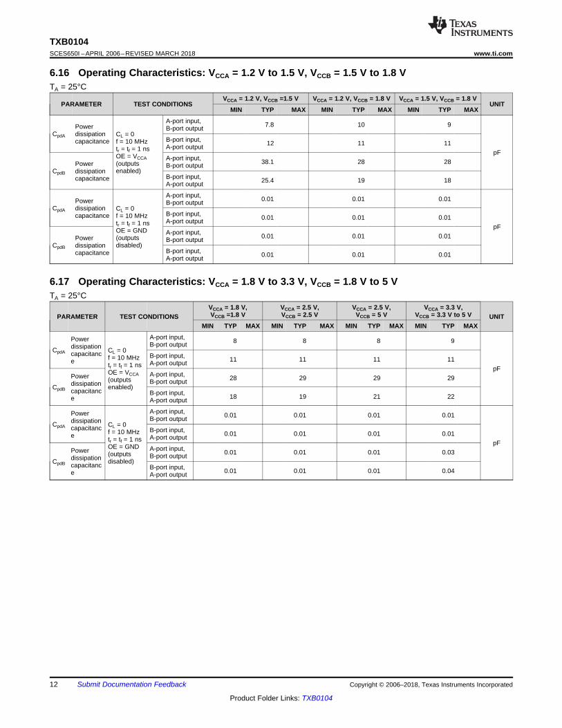
6.16 Operating Characteristics: VCCA = 1.2 V to 1.5 V, VCCB = 1.5 V to 1.8 VTA = 25°C
PARAMETER TEST CONDITIONSVCCA = 1.2 V, VCCB =1.5 V VCCA = 1.2 V, VCCB = 1.8 V VCCA = 1.5 V, VCCB = 1.8 V
UNITMIN TYP MAX MIN TYP MAX MIN TYP MAX
CpdA
Powerdissipationcapacitance
CL = 0f = 10 MHztr = tf = 1 nsOE = VCCA(outputsenabled)
A-port input,B-port output 7.8 10 9
pF
B-port input,A-port output 12 11 11
CpdB
Powerdissipationcapacitance
A-port input,B-port output 38.1 28 28
B-port input,A-port output 25.4 19 18
CpdA
Powerdissipationcapacitance
CL = 0f = 10 MHztr = tf = 1 nsOE = GND(outputsdisabled)
A-port input,B-port output 0.01 0.01 0.01
pF
B-port input,A-port output 0.01 0.01 0.01
CpdB
Powerdissipationcapacitance
A-port input,B-port output 0.01 0.01 0.01
B-port input,A-port output 0.01 0.01 0.01
6.17 Operating Characteristics: VCCA = 1.8 V to 3.3 V, VCCB = 1.8 V to 5 VTA = 25°C
PARAMETER TEST CONDITIONSVCCA = 1.8 V,VCCB =1.8 V
VCCA = 2.5 V,VCCB = 2.5 V
VCCA = 2.5 V,VCCB = 5 V
VCCA = 3.3 V,VCCB = 3.3 V to 5 V UNIT
MIN TYP MAX MIN TYP MAX MIN TYP MAX MIN TYP MAX
CpdA
Powerdissipationcapacitance
CL = 0f = 10 MHztr = tf = 1 nsOE = VCCA(outputsenabled)
A-port input,B-port output 8 8 8 9
pF
B-port input,A-port output 11 11 11 11
CpdB
Powerdissipationcapacitance
A-port input,B-port output 28 29 29 29
B-port input,A-port output 18 19 21 22
CpdA
Powerdissipationcapacitance
CL = 0f = 10 MHztr = tf = 1 nsOE = GND(outputsdisabled)
A-port input,B-port output 0.01 0.01 0.01 0.01
pF
B-port input,A-port output 0.01 0.01 0.01 0.01
CpdB
Powerdissipationcapacitance
A-port input,B-port output 0.01 0.01 0.01 0.03
B-port input,A-port output 0.01 0.01 0.01 0.04
VCCB (V)
B P
ort I
/O C
apac
itanc
e (p
F)
0 0.5 1 1.5 2 2.5 3 3.5 4 4.5 5 5.50
2
4
6
8
10
12
D003
4025qC (Room Temperature)85qC
VCCA (V)
A P
ort I
/O C
apac
itanc
e (p
F)
0 0.5 1 1.5 2 2.5 3 3.5 40
1
2
3
4
5
6
D002
4025qC (Room Temperature)85qC
VCCA (V)
OE
Pin
Inpu
t Cap
acita
nce
(pF
)
0 0.5 1 1.5 2 2.5 3 3.5 40
1
2
3
4
5
6
D001
4025qC (Room Temperature)85qC
13
TXB0104www.ti.com SCES650I –APRIL 2006–REVISED MARCH 2018
Product Folder Links: TXB0104
Submit Documentation FeedbackCopyright © 2006–2018, Texas Instruments Incorporated
6.18 Typical Characteristics
VCCB= 3.3 V
Figure 1. Input Capacitance for OE Pin (CI) vs Power Supply(VCCA)
VCCB= 3.3 V
Figure 2. Capacitance for A port I/O Pins (CiO) vs PowerSupply (VCCA)
VCCA= 1.8 V
Figure 3. Capacitance for B Port I/O Pins (CiO) vs Power Supply (VCCB)
From OutputUnder Test
15 pF 50 k
S1Open
2 x VCCO
50 k
15 pF
From OutputUnder Test
1 M
14
TXB0104SCES650I –APRIL 2006–REVISED MARCH 2018 www.ti.com
Product Folder Links: TXB0104
Submit Documentation Feedback Copyright © 2006–2018, Texas Instruments Incorporated
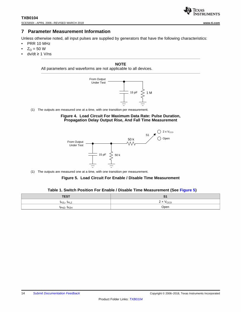
7 Parameter Measurement InformationUnless otherwise noted, all input pulses are supplied by generators that have the following characteristics:• PRR 10 MHz• ZO = 50 W• dv/dt ≥ 1 V/ns
NOTEAll parameters and waveforms are not applicable to all devices.
(1) The outputs are measured one at a time, with one transition per measurement.
Figure 4. Load Circuit For Maximum Data Rate: Pulse Duration,Propagation Delay Output Rise, And Fall Time Measurement
(1) The outputs are measured one at a time, with one transition per measurement.
Figure 5. Load Circuit For Enable / Disable Time Measurement
Table 1. Switch Position For Enable / Disable Time Measurement (See Figure 5)TEST S1
tPZL, tPLZ 2 × VCCO
tPHZ, tPZH Open
VCCI
0 V
Input
tw
VCCI / 2 VCCI / 2
tPLH tPHL
0 V
VCCO / 2
VCCI / 2 VCCI / 2
0.9 VCCOVCCO / 2
tr
0.1 VCCO
tf
VCCIInput
OutputVOH
VOL
15
TXB0104www.ti.com SCES650I –APRIL 2006–REVISED MARCH 2018
Product Folder Links: TXB0104
Submit Documentation FeedbackCopyright © 2006–2018, Texas Instruments Incorporated
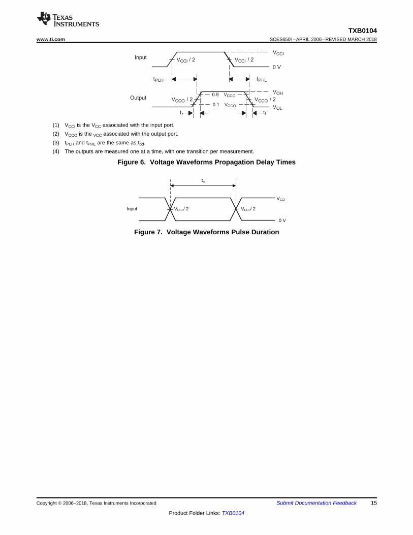
(1) VCCI is the VCC associated with the input port.(2) VCCO is the VCC associated with the output port.(3) tPLH and tPHL are the same as tpd.(4) The outputs are measured one at a time, with one transition per measurement.
Figure 6. Voltage Waveforms Propagation Delay Times
Figure 7. Voltage Waveforms Pulse Duration
VCCA VCCB
OneShot
4 k
OneShot
OneShot
OneShot
4 k
4 k
4 k
OneShot
4 k
OneShot
4 k
A2A3
A1
B2B3
B1
OE
2 channels
A4 B4
16
TXB0104SCES650I –APRIL 2006–REVISED MARCH 2018 www.ti.com
Product Folder Links: TXB0104
Submit Documentation Feedback Copyright © 2006–2018, Texas Instruments Incorporated
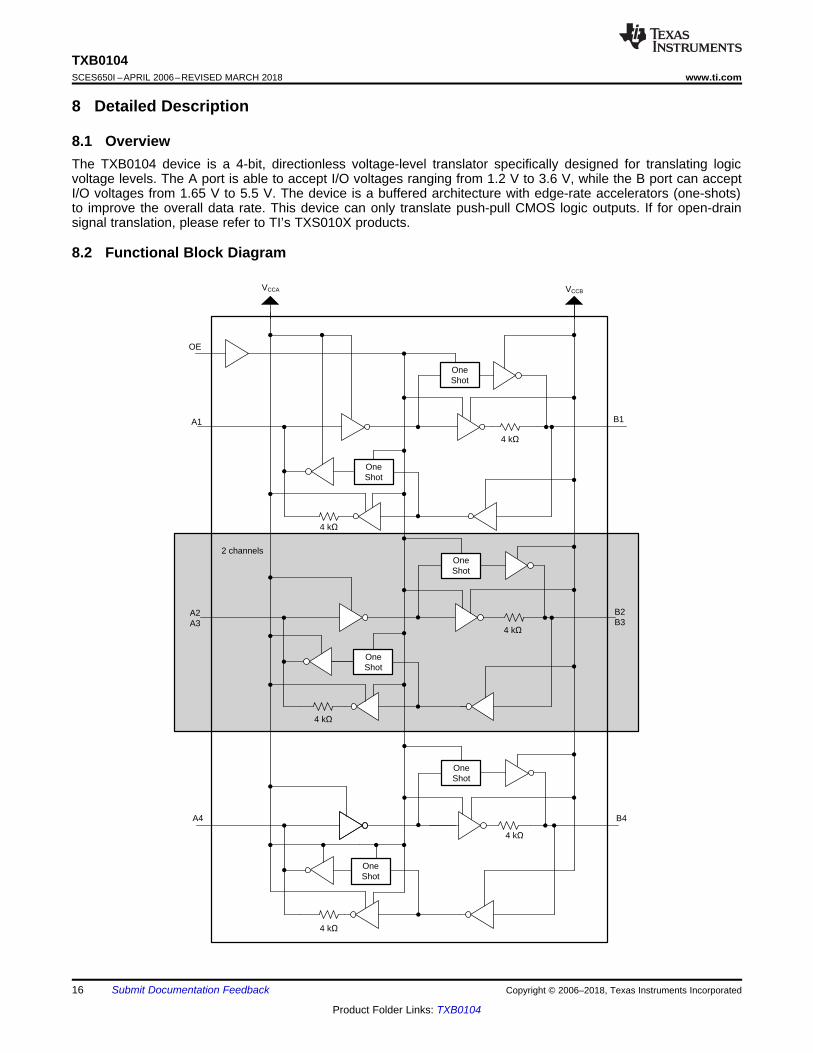
8 Detailed Description
8.1 OverviewThe TXB0104 device is a 4-bit, directionless voltage-level translator specifically designed for translating logicvoltage levels. The A port is able to accept I/O voltages ranging from 1.2 V to 3.6 V, while the B port can acceptI/O voltages from 1.65 V to 5.5 V. The device is a buffered architecture with edge-rate accelerators (one-shots)to improve the overall data rate. This device can only translate push-pull CMOS logic outputs. If for open-drainsignal translation, please refer to TI’s TXS010X products.
8.2 Functional Block Diagram
4k
4k
A B
VCCA VCCB
One
Shot
One
Shot
One
Shot
One
Shot
T1
T2
T3
T4
17
TXB0104www.ti.com SCES650I –APRIL 2006–REVISED MARCH 2018
Product Folder Links: TXB0104
Submit Documentation FeedbackCopyright © 2006–2018, Texas Instruments Incorporated
8.3 Feature Description
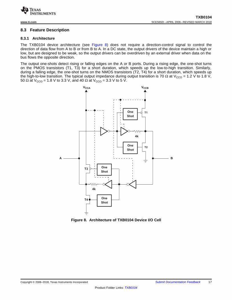
8.3.1 ArchitectureThe TXB0104 device architecture (see Figure 8) does not require a direction-control signal to control thedirection of data flow from A to B or from B to A. In a DC state, the output drivers of the device maintain a high orlow, but are designed to be weak, so the output drivers can be overdriven by an external driver when data on thebus flows the opposite direction.
The output one-shots detect rising or falling edges on the A or B ports. During a rising edge, the one-shot turnson the PMOS transistors (T1, T3) for a short duration, which speeds up the low-to-high transition. Similarly,during a falling edge, the one-shot turns on the NMOS transistors (T2, T4) for a short duration, which speeds upthe high-to-low transition. The typical output impedance during output transition is 70 Ω at VCCO = 1.2 V to 1.8 V,50 Ω at VCCO = 1.8 V to 3.3 V, and 40 Ω at VCCO = 3.3 V to 5 V.
Figure 8. Architecture of TXB0104 Device I/O Cell
IIN
VIN
VT /4 k
±(VD ± VT)/4 k
18
TXB0104SCES650I –APRIL 2006–REVISED MARCH 2018 www.ti.com
Product Folder Links: TXB0104
Submit Documentation Feedback Copyright © 2006–2018, Texas Instruments Incorporated
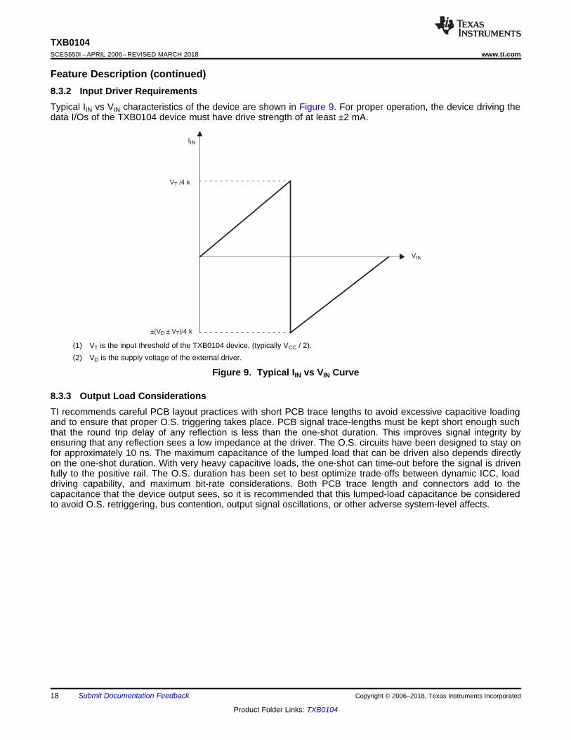
Feature Description (continued)8.3.2 Input Driver RequirementsTypical IIN vs VIN characteristics of the device are shown in Figure 9. For proper operation, the device driving thedata I/Os of the TXB0104 device must have drive strength of at least ±2 mA.
(1) VT is the input threshold of the TXB0104 device, (typically VCC / 2).(2) VD is the supply voltage of the external driver.
Figure 9. Typical IIN vs VIN Curve
8.3.3 Output Load ConsiderationsTI recommends careful PCB layout practices with short PCB trace lengths to avoid excessive capacitive loadingand to ensure that proper O.S. triggering takes place. PCB signal trace-lengths must be kept short enough suchthat the round trip delay of any reflection is less than the one-shot duration. This improves signal integrity byensuring that any reflection sees a low impedance at the driver. The O.S. circuits have been designed to stay onfor approximately 10 ns. The maximum capacitance of the lumped load that can be driven also depends directlyon the one-shot duration. With very heavy capacitive loads, the one-shot can time-out before the signal is drivenfully to the positive rail. The O.S. duration has been set to best optimize trade-offs between dynamic ICC, loaddriving capability, and maximum bit-rate considerations. Both PCB trace length and connectors add to thecapacitance that the device output sees, so it is recommended that this lumped-load capacitance be consideredto avoid O.S. retriggering, bus contention, output signal oscillations, or other adverse system-level affects.

19
TXB0104www.ti.com SCES650I –APRIL 2006–REVISED MARCH 2018
Product Folder Links: TXB0104
Submit Documentation FeedbackCopyright © 2006–2018, Texas Instruments Incorporated
Feature Description (continued)8.3.4 Enable and DisableThe TXB0104 device has an OE input that is used to disable the device by setting OE = low, which places allI/Os in the high-impedance (Hi-Z) state. The disable time (tdis) indicates the delay between when OE goes lowand when the outputs acutally get disabled (Hi-Z). The enable time (ten) indicates the amount of time the usermust allow for the one-shot circuitry to become operational after OE is taken high.
8.3.5 Pullup or Pulldown Resistors on I/O LinesThe device is designed to drive capacitive loads of up to 70 pF. The output drivers of the TXB0104 device havelow dc drive strength. If pullup or pulldown resistors are connected externally to the data I/Os, their values mustbe kept higher than 50 kΩ to ensure that they do not contend with the output drivers of the TXB0104 device.
For the same reason, the TXB0104 device must not be used in applications such as I2C or 1-Wire where anopen-drain driver is connected on the bidirectional data I/O. For these applications, use a device from the TITXS01xx series of level translators.
8.4 Device Functional ModesThe device has two functional modes, enabled and disabled. To disable the device, set the OE input to low,which places all I/Os in a high impedance state. Setting the OE input to high will enable the device.
1.8 VSystem Controller
TXB01043.3 V
System
0.1 F
3.3 V
0.1 F
1.8 V
VCCA VCCB
OE
GND
Data Data
20
TXB0104SCES650I –APRIL 2006–REVISED MARCH 2018 www.ti.com
Product Folder Links: TXB0104
Submit Documentation Feedback Copyright © 2006–2018, Texas Instruments Incorporated
9 Application and Implementation
NOTEInformation in the following applications sections is not part of the TI componentspecification, and TI does not warrant its accuracy or completeness. TI’s customers areresponsible for determining suitability of components for their purposes. Customers mustvalidate and test their design implementation to confirm system functionality.
9.1 Application InformationThe TXB0104 device can be used in level-translation applications for interfacing devices or systems operating atdifferent interface voltages with one another. It can only translate push-pull CMOS logic outputs. If for open-drainsignal translation, please refer to TI TXS010X products. Any external pulldown or pullup resistors arerecommended larger than 50 kΩ.
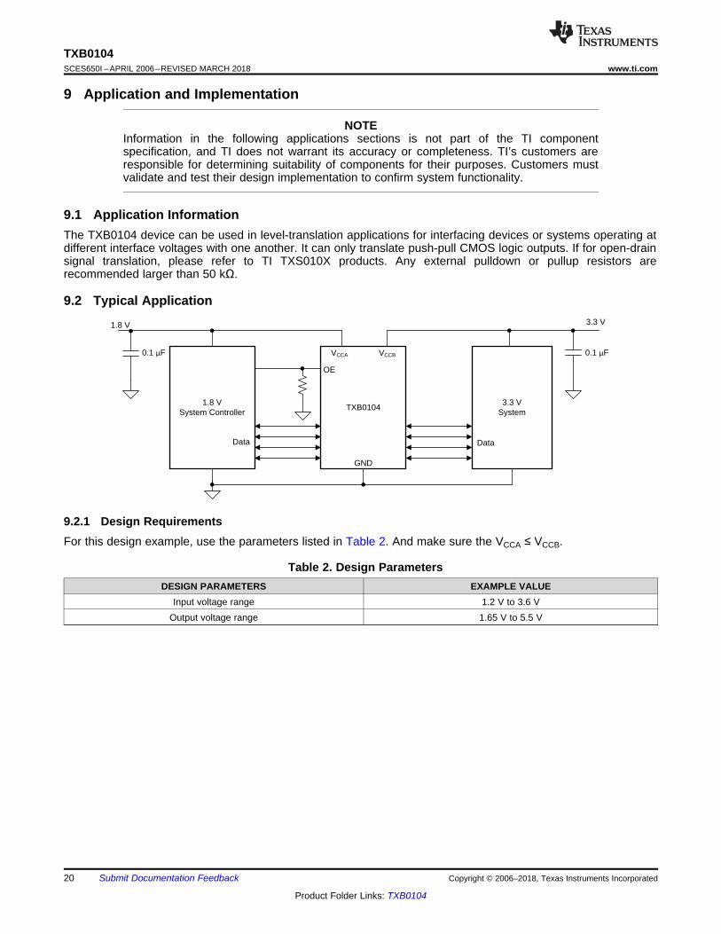
9.2 Typical Application
9.2.1 Design RequirementsFor this design example, use the parameters listed in Table 2. And make sure the VCCA ≤ VCCB.
Table 2. Design ParametersDESIGN PARAMETERS EXAMPLE VALUE
Input voltage range 1.2 V to 3.6 VOutput voltage range 1.65 V to 5.5 V
21
TXB0104www.ti.com SCES650I –APRIL 2006–REVISED MARCH 2018
Product Folder Links: TXB0104
Submit Documentation FeedbackCopyright © 2006–2018, Texas Instruments Incorporated
9.2.2 Detailed Design ProcedureTo begin the design process, determine the following:
• Input voltage range- Use the supply voltage of the device that is driving the TXB0104 device to determine the input voltagerange. For a valid logic high, the value must exceed the VIH of the input port. For a valid logic low, the valuemust be less than the VIL of the input port.
• Output voltage range- Use the supply voltage of the device that the device is driving to determine the output voltage range.- External pullup or pulldown resistors are not recommended. If mandatory, it is recommended that the valuemust be larger than 50 kΩ.
• An external pulldown or pullup resistor decreases the output VOH and VOL. Use the below equations to draftestimate the VOH and VOL as a result of an external pulldown and pullup resistor.
VOH = VCCx × RPD / (RPD + 4.5 kΩ)VOL = VCCx × 4.5 kΩ / (RPU + 4.5 kΩ)Where
• VCCx is the output port supply voltage on either VCCA or VCCB• RPD is the value of the external pull down resistor• RPU is the value of the external pull up resistor• 4.5 kΩ is the counting the variation of the serial resistor 4 kΩ in the I/O line.
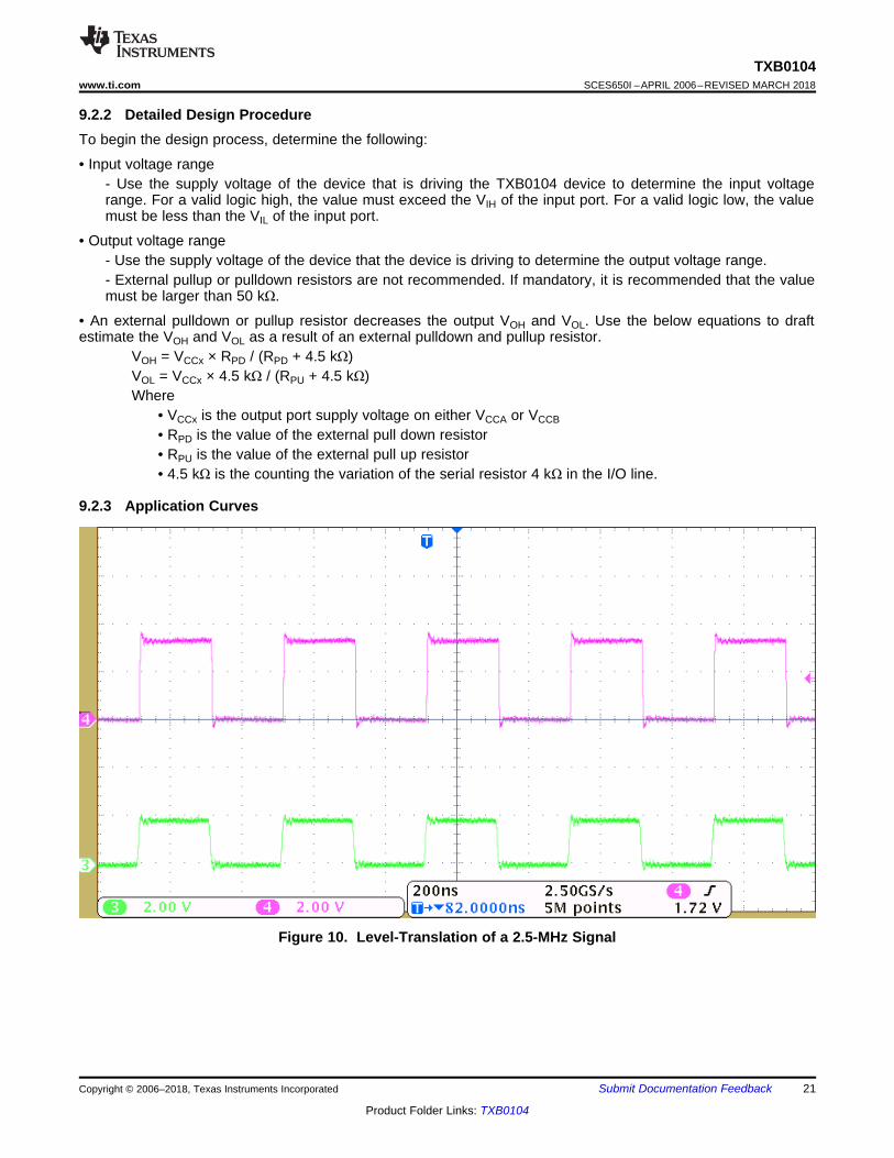
9.2.3 Application Curves
Figure 10. Level-Translation of a 2.5-MHz Signal
1
2
3
4
5
6
7
14
13
12
11
10
9
8
0.1 F 0.1 F
To Controller
To Controller
To Controller
To Controller
BypassCapacitor
BypassCapacitor
TXB0104PWR
VCCA VCCB
A1
A2
A3
A4
NC
GND
B1
B2
B3
B4
NC
OE
To System
To System
To System
To System
LEGENDPolygonal Copper Pour
VIA to Power Plane
VIA to GND Plane (Inner Layer)
Keep OE low until VCCA and VCCB are powered up
22
TXB0104SCES650I –APRIL 2006–REVISED MARCH 2018 www.ti.com
Product Folder Links: TXB0104
Submit Documentation Feedback Copyright © 2006–2018, Texas Instruments Incorporated
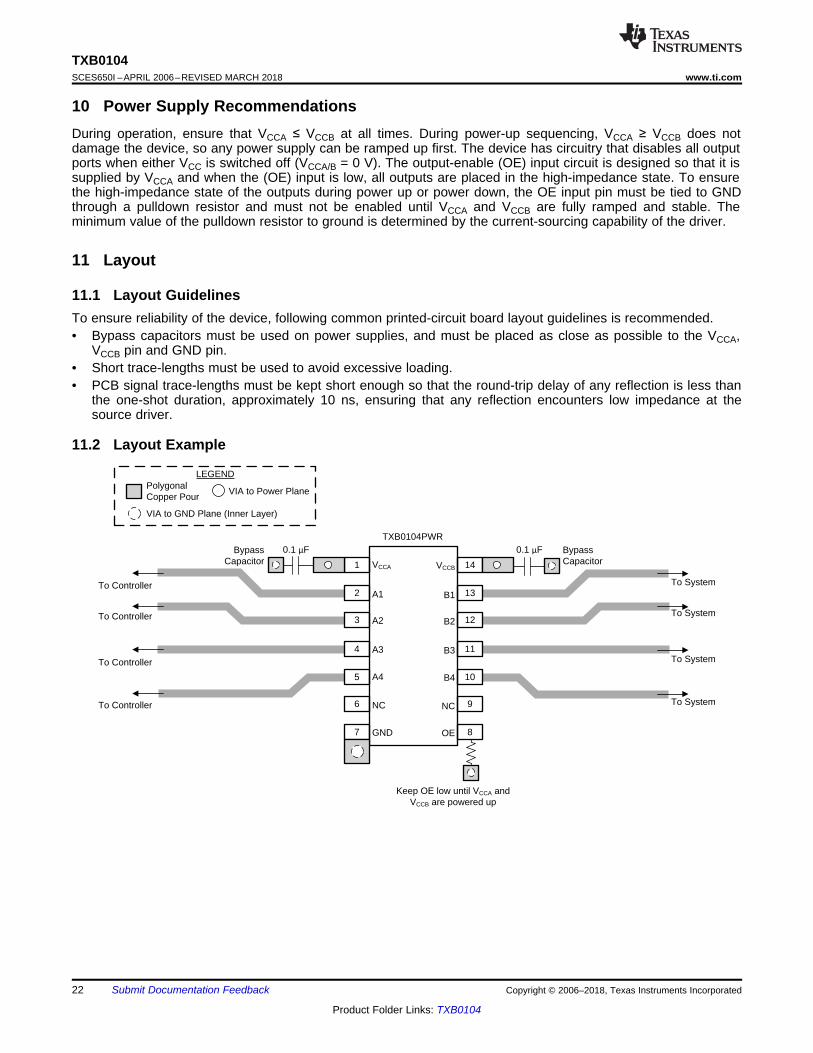
10 Power Supply RecommendationsDuring operation, ensure that VCCA ≤ VCCB at all times. During power-up sequencing, VCCA ≥ VCCB does notdamage the device, so any power supply can be ramped up first. The device has circuitry that disables all outputports when either VCC is switched off (VCCA/B = 0 V). The output-enable (OE) input circuit is designed so that it issupplied by VCCA and when the (OE) input is low, all outputs are placed in the high-impedance state. To ensurethe high-impedance state of the outputs during power up or power down, the OE input pin must be tied to GNDthrough a pulldown resistor and must not be enabled until VCCA and VCCB are fully ramped and stable. Theminimum value of the pulldown resistor to ground is determined by the current-sourcing capability of the driver.
11 Layout
11.1 Layout GuidelinesTo ensure reliability of the device, following common printed-circuit board layout guidelines is recommended.• Bypass capacitors must be used on power supplies, and must be placed as close as possible to the VCCA,
VCCB pin and GND pin.• Short trace-lengths must be used to avoid excessive loading.• PCB signal trace-lengths must be kept short enough so that the round-trip delay of any reflection is less than
the one-shot duration, approximately 10 ns, ensuring that any reflection encounters low impedance at thesource driver.
11.2 Layout Example
23
TXB0104www.ti.com SCES650I –APRIL 2006–REVISED MARCH 2018
Product Folder Links: TXB0104
Submit Documentation FeedbackCopyright © 2006–2018, Texas Instruments Incorporated
12 Device and Documentation Support
12.1 Receiving Notification of Documentation UpdatesTo receive notification of documentation updates, navigate to the device product folder on ti.com. In the upperright corner, click on Alert me to register and receive a weekly digest of any product information that haschanged. For change details, review the revision history included in any revised document.
12.2 Community ResourcesThe following links connect to TI community resources. Linked contents are provided "AS IS" by the respectivecontributors. They do not constitute TI specifications and do not necessarily reflect TI's views; see TI's Terms ofUse.
TI E2E™ Online Community TI's Engineer-to-Engineer (E2E) Community. Created to foster collaborationamong engineers. At e2e.ti.com, you can ask questions, share knowledge, explore ideas and helpsolve problems with fellow engineers.
Design Support TI's Design Support Quickly find helpful E2E forums along with design support tools andcontact information for technical support.
12.3 TrademarksE2E is a trademark of Texas Instruments.is a trademark of ~ Texas Instruments.All other trademarks are the property of their respective owners.
12.4 Electrostatic Discharge CautionThis integrated circuit can be damaged by ESD. Texas Instruments recommends that all integrated circuits be handled withappropriate precautions. Failure to observe proper handling and installation procedures can cause damage.
ESD damage can range from subtle performance degradation to complete device failure. Precision integrated circuits may be moresusceptible to damage because very small parametric changes could cause the device not to meet its published specifications.
12.5 GlossarySLYZ022 — TI Glossary.
This glossary lists and explains terms, acronyms, and definitions.
24
TXB0104SCES650I –APRIL 2006–REVISED MARCH 2018 www.ti.com
Product Folder Links: TXB0104
Submit Documentation Feedback Copyright © 2006–2018, Texas Instruments Incorporated
13 Mechanical, Packaging, and Orderable InformationThe following pages include mechanical, packaging, and orderable information. This information is the mostcurrent data available for the designated devices. This data is subject to change without notice and revision ofthis document. For browser-based versions of this data sheet, refer to the left-hand navigation.
PACKAGE OPTION ADDENDUM
www.ti.com 21-Feb-2018
Addendum-Page 1
PACKAGING INFORMATION
Orderable Device Status(1)
Package Type PackageDrawing
Pins PackageQty
Eco Plan(2)
Lead/Ball Finish(6)
MSL Peak Temp(3)
Op Temp (°C) Device Marking(4/5)
Samples
HPA01164RUTR ACTIVE UQFN RUT 12 3000 Green (RoHS& no Sb/Br)
CU NIPDAU Level-1-260C-UNLIM -40 to 85 (2KR, 2KV)
TXB0104D ACTIVE SOIC D 14 50 Green (RoHS& no Sb/Br)
CU NIPDAU Level-1-260C-UNLIM -40 to 85 TXB0104
TXB0104DG4 ACTIVE SOIC D 14 50 Green (RoHS& no Sb/Br)
CU NIPDAU Level-1-260C-UNLIM -40 to 85 TXB0104
TXB0104DR ACTIVE SOIC D 14 2500 Green (RoHS& no Sb/Br)
CU NIPDAU Level-1-260C-UNLIM -40 to 85 TXB0104
TXB0104DRG4 ACTIVE SOIC D 14 2500 Green (RoHS& no Sb/Br)
CU NIPDAU Level-1-260C-UNLIM -40 to 85 TXB0104
TXB0104PWR ACTIVE TSSOP PW 14 2000 Green (RoHS& no Sb/Br)
CU NIPDAU Level-1-260C-UNLIM -40 to 85 YE04
TXB0104PWRG4 ACTIVE TSSOP PW 14 2000 Green (RoHS& no Sb/Br)
CU NIPDAU Level-1-260C-UNLIM -40 to 85 YE04
TXB0104RGYR ACTIVE VQFN RGY 14 3000 Green (RoHS& no Sb/Br)
CU NIPDAU Level-2-260C-1 YEAR -40 to 85 YE04
TXB0104RGYRG4 ACTIVE VQFN RGY 14 3000 Green (RoHS& no Sb/Br)
CU NIPDAU Level-2-260C-1 YEAR -40 to 85 YE04
TXB0104RUTR ACTIVE UQFN RUT 12 3000 Green (RoHS& no Sb/Br)
CU NIPDAU |CU NIPDAUAG
Level-1-260C-UNLIM -40 to 85 (2KR, 2KV)
TXB0104YZTR ACTIVE DSBGA YZT 12 3000 Green (RoHS& no Sb/Br)
SNAGCU Level-1-260C-UNLIM -40 to 85 (2K, 2K7)
TXB0104ZXUR ACTIVE BGAMICROSTAR
JUNIOR
ZXU 12 2500 Green (RoHS& no Sb/Br)
SNAGCU Level-1-260C-UNLIM -40 to 85 YE04
(1) The marketing status values are defined as follows:ACTIVE: Product device recommended for new designs.LIFEBUY: TI has announced that the device will be discontinued, and a lifetime-buy period is in effect.NRND: Not recommended for new designs. Device is in production to support existing customers, but TI does not recommend using this part in a new design.PREVIEW: Device has been announced but is not in production. Samples may or may not be available.OBSOLETE: TI has discontinued the production of the device.
(2) RoHS: TI defines "RoHS" to mean semiconductor products that are compliant with the current EU RoHS requirements for all 10 RoHS substances, including the requirement that RoHS substancedo not exceed 0.1% by weight in homogeneous materials. Where designed to be soldered at high temperatures, "RoHS" products are suitable for use in specified lead-free processes. TI mayreference these types of products as "Pb-Free".
PACKAGE OPTION ADDENDUM
www.ti.com 21-Feb-2018
Addendum-Page 2
RoHS Exempt: TI defines "RoHS Exempt" to mean products that contain lead but are compliant with EU RoHS pursuant to a specific EU RoHS exemption.Green: TI defines "Green" to mean the content of Chlorine (Cl) and Bromine (Br) based flame retardants meet JS709B low halogen requirements of <=1000ppm threshold. Antimony trioxide basedflame retardants must also meet the <=1000ppm threshold requirement.
(3) MSL, Peak Temp. - The Moisture Sensitivity Level rating according to the JEDEC industry standard classifications, and peak solder temperature.
(4) There may be additional marking, which relates to the logo, the lot trace code information, or the environmental category on the device.
(5) Multiple Device Markings will be inside parentheses. Only one Device Marking contained in parentheses and separated by a "~" will appear on a device. If a line is indented then it is a continuationof the previous line and the two combined represent the entire Device Marking for that device.
(6) Lead/Ball Finish - Orderable Devices may have multiple material finish options. Finish options are separated by a vertical ruled line. Lead/Ball Finish values may wrap to two lines if the finishvalue exceeds the maximum column width.
Important Information and Disclaimer:The information provided on this page represents TI's knowledge and belief as of the date that it is provided. TI bases its knowledge and belief on informationprovided by third parties, and makes no representation or warranty as to the accuracy of such information. Efforts are underway to better integrate information from third parties. TI has taken andcontinues to take reasonable steps to provide representative and accurate information but may not have conducted destructive testing or chemical analysis on incoming materials and chemicals.TI and TI suppliers consider certain information to be proprietary, and thus CAS numbers and other limited information may not be available for release.
In no event shall TI's liability arising out of such information exceed the total purchase price of the TI part(s) at issue in this document sold by TI to Customer on an annual basis.
OTHER QUALIFIED VERSIONS OF TXB0104 :
• Automotive: TXB0104-Q1
NOTE: Qualified Version Definitions:
• Automotive - Q100 devices qualified for high-reliability automotive applications targeting zero defects
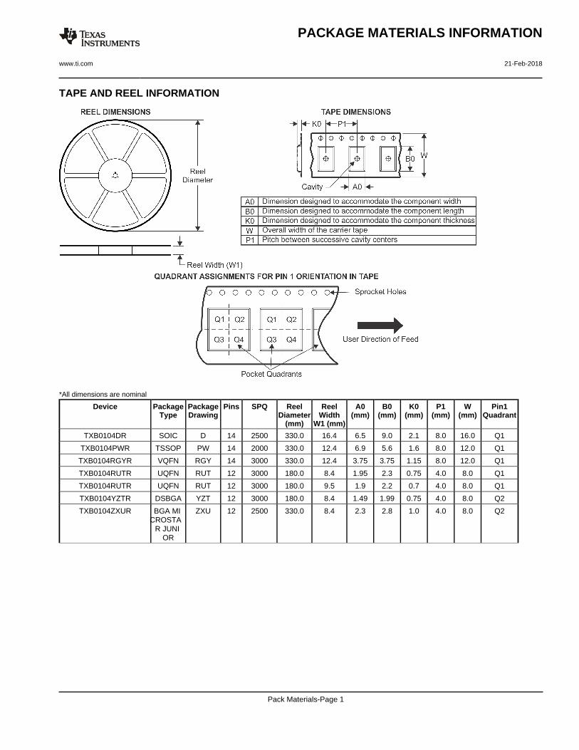
TAPE AND REEL INFORMATION
*All dimensions are nominal
Device PackageType
PackageDrawing
Pins SPQ ReelDiameter
(mm)
ReelWidth
W1 (mm)
A0(mm)
B0(mm)
K0(mm)
P1(mm)
W(mm)
Pin1Quadrant
TXB0104DR SOIC D 14 2500 330.0 16.4 6.5 9.0 2.1 8.0 16.0 Q1
TXB0104PWR TSSOP PW 14 2000 330.0 12.4 6.9 5.6 1.6 8.0 12.0 Q1
TXB0104RGYR VQFN RGY 14 3000 330.0 12.4 3.75 3.75 1.15 8.0 12.0 Q1
TXB0104RUTR UQFN RUT 12 3000 180.0 8.4 1.95 2.3 0.75 4.0 8.0 Q1
TXB0104RUTR UQFN RUT 12 3000 180.0 9.5 1.9 2.2 0.7 4.0 8.0 Q1
TXB0104YZTR DSBGA YZT 12 3000 180.0 8.4 1.49 1.99 0.75 4.0 8.0 Q2
TXB0104ZXUR BGA MI CROSTA
R JUNI OR
ZXU 12 2500 330.0 8.4 2.3 2.8 1.0 4.0 8.0 Q2
PACKAGE MATERIALS INFORMATION
www.ti.com 21-Feb-2018
Pack Materials-Page 1
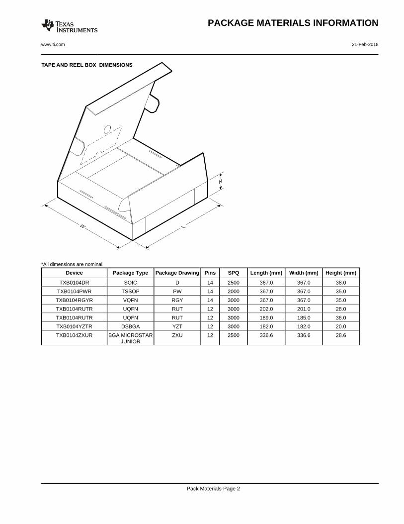
*All dimensions are nominal
Device Package Type Package Drawing Pins SPQ Length (mm) Width (mm) Height (mm)
TXB0104DR SOIC D 14 2500 367.0 367.0 38.0
TXB0104PWR TSSOP PW 14 2000 367.0 367.0 35.0
TXB0104RGYR VQFN RGY 14 3000 367.0 367.0 35.0
TXB0104RUTR UQFN RUT 12 3000 202.0 201.0 28.0
TXB0104RUTR UQFN RUT 12 3000 189.0 185.0 36.0
TXB0104YZTR DSBGA YZT 12 3000 182.0 182.0 20.0
TXB0104ZXUR BGA MICROSTARJUNIOR
ZXU 12 2500 336.6 336.6 28.6
PACKAGE MATERIALS INFORMATION
www.ti.com 21-Feb-2018
Pack Materials-Page 2
IMPORTANT NOTICE
Texas Instruments Incorporated (TI) reserves the right to make corrections, enhancements, improvements and other changes to itssemiconductor products and services per JESD46, latest issue, and to discontinue any product or service per JESD48, latest issue. Buyersshould obtain the latest relevant information before placing orders and should verify that such information is current and complete.TI’s published terms of sale for semiconductor products (http://www.ti.com/sc/docs/stdterms.htm) apply to the sale of packaged integratedcircuit products that TI has qualified and released to market. Additional terms may apply to the use or sale of other types of TI products andservices.Reproduction of significant portions of TI information in TI data sheets is permissible only if reproduction is without alteration and isaccompanied by all associated warranties, conditions, limitations, and notices. TI is not responsible or liable for such reproduceddocumentation. Information of third parties may be subject to additional restrictions. Resale of TI products or services with statementsdifferent from or beyond the parameters stated by TI for that product or service voids all express and any implied warranties for theassociated TI product or service and is an unfair and deceptive business practice. TI is not responsible or liable for any such statements.Buyers and others who are developing systems that incorporate TI products (collectively, “Designers”) understand and agree that Designersremain responsible for using their independent analysis, evaluation and judgment in designing their applications and that Designers havefull and exclusive responsibility to assure the safety of Designers' applications and compliance of their applications (and of all TI productsused in or for Designers’ applications) with all applicable regulations, laws and other applicable requirements. Designer represents that, withrespect to their applications, Designer has all the necessary expertise to create and implement safeguards that (1) anticipate dangerousconsequences of failures, (2) monitor failures and their consequences, and (3) lessen the likelihood of failures that might cause harm andtake appropriate actions. Designer agrees that prior to using or distributing any applications that include TI products, Designer willthoroughly test such applications and the functionality of such TI products as used in such applications.TI’s provision of technical, application or other design advice, quality characterization, reliability data or other services or information,including, but not limited to, reference designs and materials relating to evaluation modules, (collectively, “TI Resources”) are intended toassist designers who are developing applications that incorporate TI products; by downloading, accessing or using TI Resources in anyway, Designer (individually or, if Designer is acting on behalf of a company, Designer’s company) agrees to use any particular TI Resourcesolely for this purpose and subject to the terms of this Notice.TI’s provision of TI Resources does not expand or otherwise alter TI’s applicable published warranties or warranty disclaimers for TIproducts, and no additional obligations or liabilities arise from TI providing such TI Resources. TI reserves the right to make corrections,enhancements, improvements and other changes to its TI Resources. TI has not conducted any testing other than that specificallydescribed in the published documentation for a particular TI Resource.Designer is authorized to use, copy and modify any individual TI Resource only in connection with the development of applications thatinclude the TI product(s) identified in such TI Resource. NO OTHER LICENSE, EXPRESS OR IMPLIED, BY ESTOPPEL OR OTHERWISETO ANY OTHER TI INTELLECTUAL PROPERTY RIGHT, AND NO LICENSE TO ANY TECHNOLOGY OR INTELLECTUAL PROPERTYRIGHT OF TI OR ANY THIRD PARTY IS GRANTED HEREIN, including but not limited to any patent right, copyright, mask work right, orother intellectual property right relating to any combination, machine, or process in which TI products or services are used. Informationregarding or referencing third-party products or services does not constitute a license to use such products or services, or a warranty orendorsement thereof. Use of TI Resources may require a license from a third party under the patents or other intellectual property of thethird party, or a license from TI under the patents or other intellectual property of TI.TI RESOURCES ARE PROVIDED “AS IS” AND WITH ALL FAULTS. TI DISCLAIMS ALL OTHER WARRANTIES ORREPRESENTATIONS, EXPRESS OR IMPLIED, REGARDING RESOURCES OR USE THEREOF, INCLUDING BUT NOT LIMITED TOACCURACY OR COMPLETENESS, TITLE, ANY EPIDEMIC FAILURE WARRANTY AND ANY IMPLIED WARRANTIES OFMERCHANTABILITY, FITNESS FOR A PARTICULAR PURPOSE, AND NON-INFRINGEMENT OF ANY THIRD PARTY INTELLECTUALPROPERTY RIGHTS. TI SHALL NOT BE LIABLE FOR AND SHALL NOT DEFEND OR INDEMNIFY DESIGNER AGAINST ANY CLAIM,INCLUDING BUT NOT LIMITED TO ANY INFRINGEMENT CLAIM THAT RELATES TO OR IS BASED ON ANY COMBINATION OFPRODUCTS EVEN IF DESCRIBED IN TI RESOURCES OR OTHERWISE. IN NO EVENT SHALL TI BE LIABLE FOR ANY ACTUAL,DIRECT, SPECIAL, COLLATERAL, INDIRECT, PUNITIVE, INCIDENTAL, CONSEQUENTIAL OR EXEMPLARY DAMAGES INCONNECTION WITH OR ARISING OUT OF TI RESOURCES OR USE THEREOF, AND REGARDLESS OF WHETHER TI HAS BEENADVISED OF THE POSSIBILITY OF SUCH DAMAGES.Unless TI has explicitly designated an individual product as meeting the requirements of a particular industry standard (e.g., ISO/TS 16949and ISO 26262), TI is not responsible for any failure to meet such industry standard requirements.Where TI specifically promotes products as facilitating functional safety or as compliant with industry functional safety standards, suchproducts are intended to help enable customers to design and create their own applications that meet applicable functional safety standardsand requirements. Using products in an application does not by itself establish any safety features in the application. Designers mustensure compliance with safety-related requirements and standards applicable to their applications. Designer may not use any TI products inlife-critical medical equipment unless authorized officers of the parties have executed a special contract specifically governing such use.Life-critical medical equipment is medical equipment where failure of such equipment would cause serious bodily injury or death (e.g., lifesupport, pacemakers, defibrillators, heart pumps, neurostimulators, and implantables). Such equipment includes, without limitation, allmedical devices identified by the U.S. Food and Drug Administration as Class III devices and equivalent classifications outside the U.S.TI may expressly designate certain products as completing a particular qualification (e.g., Q100, Military Grade, or Enhanced Product).Designers agree that it has the necessary expertise to select the product with the appropriate qualification designation for their applicationsand that proper product selection is at Designers’ own risk. Designers are solely responsible for compliance with all legal and regulatoryrequirements in connection with such selection.Designer will fully indemnify TI and its representatives against any damages, costs, losses, and/or liabilities arising out of Designer’s non-compliance with the terms and provisions of this Notice.
Mailing Address: Texas Instruments, Post Office Box 655303, Dallas, Texas 75265Copyright © 2018, Texas Instruments Incorporated