ts5a22364 datasheet - ti.com · input select shunt switch in2 in1 com2 com1 nc2 nc1 no2 out+ out+...
TRANSCRIPT
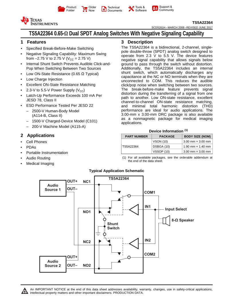
Input Select
ShuntSwitch
IN2
IN1
COM2
COM1
NC2
NC1
NO2
OUT+
OUT+
OUT–
OUT–
NO1
TS5A22364
AudioSource 1
AudioSource 2
8- SpeakerΩ
Product
Folder
Order
Now
Technical
Documents
Tools &
Software
Support &Community
An IMPORTANT NOTICE at the end of this data sheet addresses availability, warranty, changes, use in safety-critical applications,intellectual property matters and other important disclaimers. PRODUCTION DATA.
TS5A22364SCDS261H –MARCH 2008–REVISED JUNE 2017
TS5A22364 0.65-Ω Dual SPDT Analog Switches With Negative Signaling Capability
1
1 Features1• Specified Break-Before-Make Switching• Negative Signaling Capability: Maximum Swing
from –2.75 V to 2.75 V (VCC = 2.75 V)• Internal Shunt Switch Prevents Audible Click-and-
Pop When Switching Between Two Sources• Low ON-State Resistance (0.65 Ω Typical)• Low Charge Injection• Excellent ON-State Resistance Matching• 2.3-V to 5.5-V Power Supply (VCC)• Latch-Up Performance Exceeds 100 mA Per
JESD 78, Class II• ESD Performance Tested Per JESD 22
– 2500-V Human-Body Model(A114-B, Class II)
– 1500-V Charged-Device Model (C101)– 200-V Machine Model (A115-A)
2 Applications• Cell Phones• PDAs• Portable Instrumentation• Audio Routing• Medical Imaging
3 DescriptionThe TS5A22364 is a bidirectional, 2-channel, single-pole double-throw (SPDT) analog switch designed tooperate from 2.3 V to 5.5 V. The device featuresnegative signal capability that allows signals belowground to pass through the switch without distortion.Additionally, the TS5A22364 includes an internalshunt switch, which automatically discharges anycapacitance at the NC or NO terminals when they areunconnected to COM. This reduces the audibleclick/pop noise when switching between two sources.The break-before-make feature prevents signaldistortion during the transferring of a signal from onepath to another. Low ON-state resistance, excellentchannel-to-channel ON-state resistance matching,and minimal total harmonic distortion (THD)performance are ideal for audio applications. The3.00-mm x 3.00-mm DRC package is also availableas a nonmagnetic package for medical imagingapplications.
Device Information (1)
PART NUMBER PACKAGE BODY SIZE (NOM)
TS5A22364VSON (10) 3.00 mm × 3.00 mmDSBGA (10) 1.90 mm × 1.40 mmVSSOP (10) 3.00 mm × 3.00 mm
(1) For all available packages, see the orderable addendum atthe end of the data sheet.
Typical Application Schematic

2
TS5A22364SCDS261H –MARCH 2008–REVISED JUNE 2017 www.ti.com
Product Folder Links: TS5A22364
Submit Documentation Feedback Copyright © 2008–2017, Texas Instruments Incorporated
Table of Contents1 Features .................................................................. 12 Applications ........................................................... 13 Description ............................................................. 14 Revision History..................................................... 25 Pin Configuration and Functions ......................... 36 Specifications......................................................... 4
6.1 Absolute Maximum Ratings ...................................... 46.2 ESD Ratings.............................................................. 46.3 Recommended Operating Conditions....................... 46.4 Thermal Information .................................................. 56.5 Electrical Characteristics for 2.5-V Supply................ 56.6 Electrical Characteristics for 3.3-V Supply................ 66.7 Electrical Characteristics for 5-V Supply .................. 86.8 Typical Characteristics .............................................. 9
7 Parameter Measurement Information ................ 118 Detailed Description ............................................ 15
8.1 Overview ................................................................. 15
8.2 Functional Block Diagram ....................................... 158.3 Feature Description................................................. 168.4 Device Functional Modes........................................ 16
9 Application and Implementation ........................ 179.1 Application Information............................................ 179.2 Typical Application .................................................. 17
10 Power Supply Recommendations ..................... 1911 Layout................................................................... 19
11.1 Layout Guidelines ................................................. 1911.2 Layout Example .................................................... 19
12 Device and Documentation Support ................. 2012.1 Receiving Notification of Documentation Updates 2012.2 Community Resources.......................................... 2012.3 Trademarks ........................................................... 2012.4 Electrostatic Discharge Caution............................ 2012.5 Glossary ................................................................ 20
13 Mechanical, Packaging, and OrderableInformation ........................................................... 20
4 Revision HistoryNOTE: Page numbers for previous revisions may differ from page numbers in the current version.
Changes from Revision G (September 2015) to Revision H Page
• Changed the VIN MAX value From: VCC To: 5.5 V in the Recommended Operating Conditions table .................................. 4
Changes from Revision F (June 2015) to Revision G Page
• Changed CL TEST CONDITION value for all THD PARAMETERs from 15 pf to 35 pf. ....................................................... 7
Changes from Revision E (May 2013) to Revision F Page
• Added Pin Configuration and Functions section, ESD Ratings table, Recommended Operating Conditions table,Feature Description section, Device Functional Modes, Application and Implementation section, Power SupplyRecommendations section, Layout section, Device and Documentation Support section, and Mechanical,Packaging, and Orderable Information section ...................................................................................................................... 1
• Split the TS5A22364 and TS5A22362 into separate datasheets and added verbiage to clarify the operation of theshunt resistor. ........................................................................................................................................................................ 1
• Changed the max Ron spec from 1.04 Ω to 1.30 Ω at 2.7 V VCC across full TA. ................................................................... 5
Changes from Revision D (November 2011) to Revision E Page
• Added Absolute Maximum Ratings textnote........................................................................................................................... 4
Changes from Revision C (April 2010) to Revision D Page
• Added Medical Imaging to Applications.................................................................................................................................. 1

Laser Marking View Bump View
B
C
D
3 2 1
A
B
C
D
1 2 3
A
1
2
3
4
5
10
9
8
7
6
NO2
COM2
NC2
IN2
VCC
NO1
COM1
NC1
IN1 GND
ExposedCenter
Pad
VCC
NO1
COM1
NC1
IN1
NO2
COM2
NC2
IN2
GND
1
2
3
4
5
10
9
8
7
6
3
TS5A22364www.ti.com SCDS261H –MARCH 2008–REVISED JUNE 2017
Product Folder Links: TS5A22364
Submit Documentation FeedbackCopyright © 2008–2017, Texas Instruments Incorporated
5 Pin Configuration and Functions
DRC Package10-Pin VSON
Top View
*The exposed center pad, if used, must beconnected as a secondary GND or leftelectrically open.
DGS Package10-Pin VSSOP
Top View
YZP Package10-Pin DSBGA
Top View
Pin FunctionsPIN
TYPE DESCRIPTIONNAME DRC / DGS YZPVCC 1 A2 — Power SupplyNO1 2 A3 I/O Normally Open (NO) signal path, Switch 1COM1 3 B3 I/O Common signal path, Switch 1NC1 4 C3 I/O Normally Closed (NC) signal path, Switch 1IN1 5 D3 I Digital control pin to connect COM1 to NO1, Switch 1GND 6 D2 — GroundIN2 7 D1 I Digital control pin to connect COM2 to NO2, Switch 2NC2 8 C1 I/O Normally Closed (NC) signal path, Switch 2COM2 9 B1 I/O Common signal path, Switch 2NO2 10 A1 I/O Normally Open (NO) signal Path, Switch 2

4
TS5A22364SCDS261H –MARCH 2008–REVISED JUNE 2017 www.ti.com
Product Folder Links: TS5A22364
Submit Documentation Feedback Copyright © 2008–2017, Texas Instruments Incorporated
(1) Stresses beyond those listed under Absolute Maximum Ratings may cause permanent damage to the device. These are stress ratingsonly, which do not imply functional operation of the device at these or any other conditions beyond those indicated under RecommendedOperating Conditions . Exposure to absolute-maximum-rated conditions for extended periods may affect device reliability
(2) The algebraic convention, whereby the most negative value is a minimum and the most positive value is a maximum(3) All voltages are with respect to ground, unless otherwise specified.(4) The input and output voltage ratings may be exceeded if the input and output clamp-current ratings are observed.(5) This value is limited to 5.5 V maximum.(6) Pulse at 1-ms duration < 10% duty cycle.(7) VCC = 3.0 V to 5.0 V, TA = –40°C to 85°C.(8) For YZP package only.
6 Specifications
6.1 Absolute Maximum Ratingsover operating free-air temperature range (unless otherwise noted) (1) (2)
MIN MAX UNIT
VCC Supply voltage (3) –0.5 6 V
VNCVNOVCOM
Analog voltage (3) (4) (5) VCC – 6 VCC + 0.5 V
II/OK Analog port diode currentVNC, VNO, VCOM < 0orVNC, VNO, VCOM > VCC
–50 50 mA
INCINOICOM
ON-state switch current
VNC, VNO, VCOM = 0 to VCC
–150 150
mAON-state peak switch current (6) –300 300
IRSH OFF-state switch Shunt Resistor current –20 20
INC(3) (7) (8)
INO(3) (7) (8)
ICOM(3) (7) (8)
ON-state switch currentVNC, VNO, VCOM = 0 to VCC
–350 350mA
ON-state peak switch current (6) –500 500
VIN Digital input voltage range –0.5 6.5 V
IIK Digital input clamp current (3) (4) VI < 0 –50 50 mA
ICCIGND
Continuous current through VCCor GND –100 100 mA
Tstg Storage temperature –65 150 °C
(1) JEDEC document JEP155 states that 500-V HBM allows safe manufacturing with a standard ESD control process. Manufacturing withless than 500-V HBM is possible with the necessary precautions.
(2) JEDEC document JEP157 states that 250-V CDM allows safe manufacturing with a standard ESD control process. Manufacturing withless than 250-V CDM is possible with the necessary precautions.
6.2 ESD RatingsVALUE UNIT
V(ESD) Electrostatic dischargeHuman-body model (HBM), per ANSI/ESDA/JEDEC JS-001 (1) ±2500
VCharged-device model (CDM), per JEDEC specification JESD22-C101(2) ±1500
6.3 Recommended Operating Conditionsover operating free-air temperature range (unless otherwise noted)
MIN MAX UNITVCC Supply voltage 2.3 5.5 VVNCVNOVCOM
Signal path voltage VCC – 5.5 VCC V
VIN Digital control GND 5.5 V
5
TS5A22364www.ti.com SCDS261H –MARCH 2008–REVISED JUNE 2017
Product Folder Links: TS5A22364
Submit Documentation FeedbackCopyright © 2008–2017, Texas Instruments Incorporated
(1) For more information about traditional and new thermal metrics, see the Semiconductor and IC Package Thermal Metrics applicationreport.
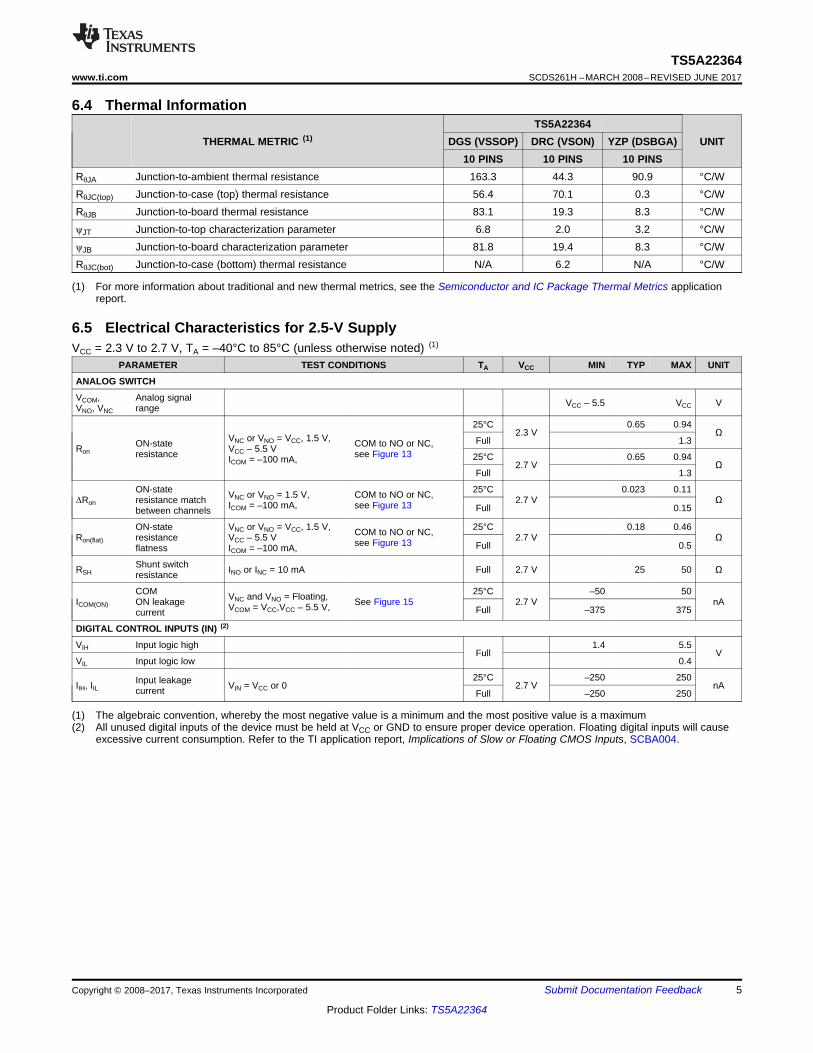
6.4 Thermal Information
THERMAL METRIC (1)TS5A22364
UNITDGS (VSSOP) DRC (VSON) YZP (DSBGA)10 PINS 10 PINS 10 PINS
RθJA Junction-to-ambient thermal resistance 163.3 44.3 90.9 °C/WRθJC(top) Junction-to-case (top) thermal resistance 56.4 70.1 0.3 °C/WRθJB Junction-to-board thermal resistance 83.1 19.3 8.3 °C/WψJT Junction-to-top characterization parameter 6.8 2.0 3.2 °C/WψJB Junction-to-board characterization parameter 81.8 19.4 8.3 °C/WRθJC(bot) Junction-to-case (bottom) thermal resistance N/A 6.2 N/A °C/W
(1) The algebraic convention, whereby the most negative value is a minimum and the most positive value is a maximum(2) All unused digital inputs of the device must be held at VCC or GND to ensure proper device operation. Floating digital inputs will cause
excessive current consumption. Refer to the TI application report, Implications of Slow or Floating CMOS Inputs, SCBA004.
6.5 Electrical Characteristics for 2.5-V SupplyVCC = 2.3 V to 2.7 V, TA = –40°C to 85°C (unless otherwise noted) (1)
PARAMETER TEST CONDITIONS TA VCC MIN TYP MAX UNIT
ANALOG SWITCH
VCOM,VNO, VNC
Analog signalrange VCC – 5.5 VCC V
RonON-stateresistance
VNC or VNO = VCC, 1.5 V,VCC – 5.5 VICOM = –100 mA,
COM to NO or NC,see Figure 13
25°C2.3 V
0.65 0.94Ω
Full 1.3
25°C2.7 V
0.65 0.94Ω
Full 1.3
ΔRon
ON-stateresistance matchbetween channels
VNC or VNO = 1.5 V,ICOM = –100 mA,
COM to NO or NC,see Figure 13
25°C2.7 V
0.023 0.11Ω
Full 0.15
Ron(flat)
ON-stateresistanceflatness
VNC or VNO = VCC, 1.5 V,VCC – 5.5 VICOM = –100 mA,
COM to NO or NC,see Figure 13
25°C2.7 V
0.18 0.46Ω
Full 0.5
RSHShunt switchresistance INO or INC = 10 mA Full 2.7 V 25 50 Ω
ICOM(ON)
COMON leakagecurrent
VNC and VNO = Floating,VCOM = VCC,VCC – 5.5 V, See Figure 15
25°C2.7 V
–50 50nA
Full –375 375
DIGITAL CONTROL INPUTS (IN) (2)
VIH Input logic highFull
1.4 5.5V
VIL Input logic low 0.4
IIH, IILInput leakagecurrent VIN = VCC or 0
25°C2.7 V
–250 250nA
Full –250 250

6
TS5A22364SCDS261H –MARCH 2008–REVISED JUNE 2017 www.ti.com
Product Folder Links: TS5A22364
Submit Documentation Feedback Copyright © 2008–2017, Texas Instruments Incorporated
Electrical Characteristics for 2.5-V Supply (continued)VCC = 2.3 V to 2.7 V, TA = –40°C to 85°C (unless otherwise noted) (1)
PARAMETER TEST CONDITIONS TA VCC MIN TYP MAX UNIT
DYNAMIC
tON Turnon time VCOM = VCC,RL = 300 Ω,
CL = 35 pF,see Figure 17
25°C 2.5 V 44 80ns
Full 2.3 V to2.7 V 120
tOFF Turnoff time VCOM = VCC,RL = 300 Ω,
CL = 35 pF,see Figure 17
25°C 2.5 V 22 70ns
Full 2.3 V to2.7 V 70
tBBMBreak-before-maketime See Figure 18 25°C 2.5 V 1 7 ns
QC Charge injection VGEN = 0, RGEN = 0 CL = 1 nF, see Figure 22 25°C 2.5 V 215 pC
CCOM(ON)NC, NO, COMON capacitance
VCOM = VCC or GND,Switch ON, f = 10 MHz See Figure 16 25°C 2.5 V 370 pF
CIDigital inputcapacitance VIN = VCC or GND See Figure 16 25°C 2.5 V 2.6 pF
BW Bandwidth RL = 50 Ω, –3 dB 25°C 2.5 V 17 MHz
OISO OFF isolation RL = 50 Ω f = 100 kHz, seeFigure 20 25°C 2.5 V –66 dB
XTALK Crosstalk RL = 50 Ω f = 100 kHz,see Figure 21 25°C 2.5 V –75 dB
THD Total harmonicdistortion
RL = 600 Ω,CL = 35 pF,
f = 20 Hz to20 kHz, see Figure 23 25°C 2.5 V 0.01%
SUPPLY
ICCPositivesupply current
VCOM and VIN = VCC or GND,VNC and VNO = Floating
25°C2.7 V
0.2 1.1μA
Full 1.3
VCOM = VCC – 5.5,VIN = VCC or GND,VNC and VNO = Floating
Full 2.7 V 3.3 μA
(1) The algebraic convention, whereby the most negative value is a minimum and the most positive value is a maximum(2) All digital inputs of the device must be held at VCC or GND to ensure proper device operation. Floating digital inputs will cause excessive
current consumption. Refer to the TI application report, Implications of Slow or Floating CMOS Inputs, SCBA004.
6.6 Electrical Characteristics for 3.3-V SupplyVCC = 3 V to 3.6 V, TA = –40°C to 85°C (unless otherwise noted) (1)
PARAMETER TEST CONDITIONS TA VCC MIN TYP MAX UNIT
ANALOG SWITCH
VCOM,VNO, VNC
Analog signalrange VCC – 5.5 VCC V
RonON-stateresistance
VNC or VNO ≤ VCC, 1.5 V,VCC – 5.5 V,ICOM = –100 mA,
COM to NO or NC,see Figure 13
25°C3 V
0.61 0.87Ω
Full 0.97
ΔRon
ON-stateresistance matchbetween channels
VNC or VNO = 1.5 V,ICOM = –100 mA,
COM to NO or NC,see Figure 13
25°C3 V
0.024 0.13Ω
Full 0.13
Ron(flat)
ON-stateresistanceflatness
VNC or VNO ≤ VCC, 1.5 V,VCC – 5.5 V,ICOM = –100 mA,
COM to NO or NC,see Figure 13
25°C3 V
0.12 0.46Ω
Full 0.5
RSHShunt switchresistance INO or INC = 10 mA Full 3 V 25 37 Ω
ICOM(ON)
COMON leakagecurrent
VNC and VNO = Open,VCOM = VCC,VCC – 5.5 V,
COM to NO or NC,see Figure 15
25°C3.6 V
–50 50nA
Full –375 375
DIGITAL CONTROL INPUTS (IN) (2)
VIH Input logic highFull
1.4 5.5V
VIL Input logic low 0.6
IIH, IIL Input leakage current VIN = VCC or 025°C
3.6 V–250 250
nAFull –250 250

7
TS5A22364www.ti.com SCDS261H –MARCH 2008–REVISED JUNE 2017
Product Folder Links: TS5A22364
Submit Documentation FeedbackCopyright © 2008–2017, Texas Instruments Incorporated
Electrical Characteristics for 3.3-V Supply (continued)VCC = 3 V to 3.6 V, TA = –40°C to 85°C (unless otherwise noted) (1)
PARAMETER TEST CONDITIONS TA VCC MIN TYP MAX UNIT
DYNAMIC
tON Turnon time VCOM = VCC,RL = 300 Ω,
CL = 35 pF,see Figure 17
25°C 3.3 V 34 80ns
Full 3 V to3.6 V 120
tOFF Turnoff time VCOM = VCC,RL = 300 Ω,
CL = 35 pF,see Figure 17
25°C 3.3 V 19 70ns
Full 3 V to3.6 V 70
tBBMBreak-before-maketime See Figure 18 25°C 3.3 V 1 7 ns
QC Charge injection VGEN = 0,RGEN = 0,
CL = 1 nF,see Figure 22 25°C 3.3 V 300 pC
CCOM(ON)NC, NO, COMON capacitance
VCOM = VCC or GND,f = 10 MHz See Figure 16 25°C 3.3 V 370 pF
CIDigital inputcapacitance VIN = VCC or GND See Figure 16 25°C 3.3 V 2.6 pF
BW Bandwidth RL = 50 Ω, –3 dB Switch ON, 25°C 3.3 V 17.5 MHz
OISO OFF isolation RL = 50 Ω, f = 100 kHz,see Figure 20 25°C 3.3 V –68 dB
XTALK Crosstalk RL = 50 Ω, f = 100 kHz,see Figure 21 25°C 3.3 V –76 dB
THD Total harmonicdistortion
RL = 600 Ω,CL = 35 pF,
f = 20 Hz to 20 kHz,see Figure 23 25°C 3.3 V 0.008%
SUPPLY
ICCPositivesupply current
VCOM and VIN = VCC or GND,VNC and VNO = Floating
25°C3.6 V
0.1 1.2μA
Full 1.3
VCOM = VCC – 5.5 V,VIN = VCC or GND,VNC and VNO = Floating
Full 3.6 V 3.4 μA

8
TS5A22364SCDS261H –MARCH 2008–REVISED JUNE 2017 www.ti.com
Product Folder Links: TS5A22364
Submit Documentation Feedback Copyright © 2008–2017, Texas Instruments Incorporated
(1) The algebraic convention, whereby the most negative value is a minimum and the most positive value is a maximum(2) All unused digital inputs of the device must be held at VCC or GND to ensure proper device operation. Floating digital inputs will cause
excessive current consumption. Refer to the TI application report, Implications of Slow or Floating CMOS Inputs, SCBA004.
6.7 Electrical Characteristics for 5-V SupplyVCC = 4.5 V to 5.5 V, TA = –40°C to 85°C (unless otherwise noted) (1)
PARAMETER TEST CONDITIONS TA VCC MIN TYP MAX UNIT
ANALOG SWITCH
VCOM,VNO, VNC
Analog signalrange VCC – 5.5 VCC V
RonON-stateresistance
VNC or VNO = VCC, 1.6 V,VCC = –5.5 V,ICOM = –100 mA,
COM to NO or NC,see Figure 13
25°C4.5 V
0.52 0.74Ω
Full 0.83
ΔRon
ON-stateresistance matchbetween channels
VNC or VNO = 1.6 V,ICOM = –100 mA,
COM to NO or NC,see Figure 13
25°C4.5 V
0.04 0.23Ω
Full 0.30
Ron(flat)
ON-stateresistanceflatness
VNC or VNO = VCC, 1.6 V,VCC = –5.5 V,ICOM = –100 mA,
COM to NO or NC,see Figure 13
25°C4.5 V
0.076 0.46Ω
Full 0.5
RSHShunt switchresistance INO or INC = 10 mA Full 4.5 V 16 36 Ω
ICOM(ON)
COMON leakagecurrent
VNC and VNO = Open,VCOM = VCC, VCC – 5.5 V, See Figure 15
25°C5.5 V
–50 50nA
Full –375 375
DIGITAL CONTROL INPUTS (IN) (2)
VIH Input logic highFull
2.4 5.5V
VIL Input logic low 0.8
IIH, IILInput leakagecurrent VIN = VCC or 0
25°C5.5 V
–250 250nA
Full –250 250
DYNAMIC
tON Turnon time VCOM = VCC,RL = 300 Ω,
CL = 35 pF,see Figure 17
25°C 5 V 27 80ns
Full 4.5 V to5.5 V 80
tOFF Turnoff time VCOM = VCC,RL = 300 Ω,
CL = 35 pF,see Figure 17
25°C 5 V 13 70ns
Full 4.5 V to5.5 V 70
tBBMBreak-before-make time
VNC = VNO = VCC/2RL = 300 Ω, CL = 35 pF, 25°C 5 V 1 3.5 ns
QC Charge injection VGEN = 0,RGEN = 0,
CL = 1 nF,see Figure 22 25°C 5 V 500 pC
CCOM(ON)NC, NO, COMON capacitance VCOM = VCC or GND, See Figure 16 25°C 5 V 370 pF
CIDigital inputcapacitance VIN = VCC or GND See Figure 16 25°C 5 V 2.6 pF
BW Bandwidth RL = 50 Ω, 25°C 5 V 18.3 MHz
OISO OFF isolation RL = 50 Ω, f = 100 kHz,see Figure 20 25°C 5 V –70 dB
XTALK Crosstalk RL = 50 Ω, f = 100 kHz,see Figure 21 25°C 5 V –78 dB
THD Total harmonicdistortion
RL = 600 Ω,CL = 35 pF,
f = 20 Hz to 20 kHz,see Figure 23 25°C 5 V 0.009%
SUPPLY
ICCPositivesupply current
VCOM and VIN = VCC or GND,VNC and VNO = Floating
25°C
5.5 V
0.2 1.3
μAFull 3.5
VCOM = VCC – 5.5,VIN = VCC or GND,VNC and VNO = Floating
Full 5

-90
-80
-70
-60
-50
-40
-30
-20
-10
0
Att
en
ua
tio
n (
dB
)
Frequency (MHz)
10001–18
–16
–14
–12
–10
–8
–6
–4
–2
0
1 1000Frequency (MHz)
Mag
nit
ud
e (
dB
)
-10.00
COM (V)
Ro
n(
)Ω
TA = 85°C
TA= 25°C
TA= -40°C
0 1 2 3 4 5
0.05
0.10
0.15
0.20
0.25
0.30
0.35
0.40
0.45
0.50
V
-3
VCOM (V)
Ro
n
)
TA = 85 qC
TA= 25 qC
TA= -40 qC
-2 -1 0 1 2 3 40.0
0.1
0.2
0.3
0.4
0.5
0.6
VCOM (V)
Ro
n
)
VCC = 2.3 V
VCC = 3.0 V
VCC = 4.5 V
1.2
1.0
0.8
0.6
0.4
0.2
0.0
-4.0 -2.0 2.00.0 4.0 6.0 VCOM (V)
Ron
()
±30.0
TA = 25°CTA =-40°C
TA = 85°C
±2 ±1 0 1 2 3
0.1
0.2
0.3
0.4
0.5
0.6
0.7
0.8
9
TS5A22364www.ti.com SCDS261H –MARCH 2008–REVISED JUNE 2017
Product Folder Links: TS5A22364
Submit Documentation FeedbackCopyright © 2008–2017, Texas Instruments Incorporated
6.8 Typical Characteristics
Figure 1. Ron vs VCOM Figure 2. Ron vs VCOM (VCC = 2.7 V)
Figure 3. Ron vs VCOM (VCC = 3.3 V) Figure 4. Ron vs VCOM (VCC = 5 V)
Figure 5. Insertion Loss Figure 6. Off Isolation vs Frequency
0
20
40
60
80
100
120
140
160
180
200
0.0 1.0 2.0 3.0 4.0 5.0 6.0
Supply Voltage (V)
tOFF
t(n
s)
ON
/tO
FF
tON
t(n
s)
ON
/tO
FF
0
5
10
15
20
25
30
35
40
45
50
–40 25 85
Temperature(°C)
tOFF
tON
0.0E+00
5.0E-09
1.0E-08
1.5E-08
2.0E-08
2.5E-08
3.0E-08
3.5E-08
0.0 0.5 1.0 1.5 2.5 3.0 3.5 4.0 4.5 5.5
I CC
(A
)μ
VCC (V)
0.0001
0.0011
0.0021
0.0031
0.0041
0.0051
0.0061
0.0071
0.0081
0.0091
10 100 1000 10000 100000
Frequency (Hz)
TH
D
-90
-80
-70
-60
-50
-40
-30
-20
-10
0
1 1000Frequency (MHz)
Att
en
uati
on
(d
B)
Voltage (V)
Ch
arg
e In
jecti
on
(p
C)
–200
–100
0
100
200
300
400
500
0 1.8 2.5 3.3 5
V = 2.5 VCC
V = 3.3 VCC
V = 5 VCC
10
TS5A22364SCDS261H –MARCH 2008–REVISED JUNE 2017 www.ti.com
Product Folder Links: TS5A22364
Submit Documentation Feedback Copyright © 2008–2017, Texas Instruments Incorporated
Typical Characteristics (continued)
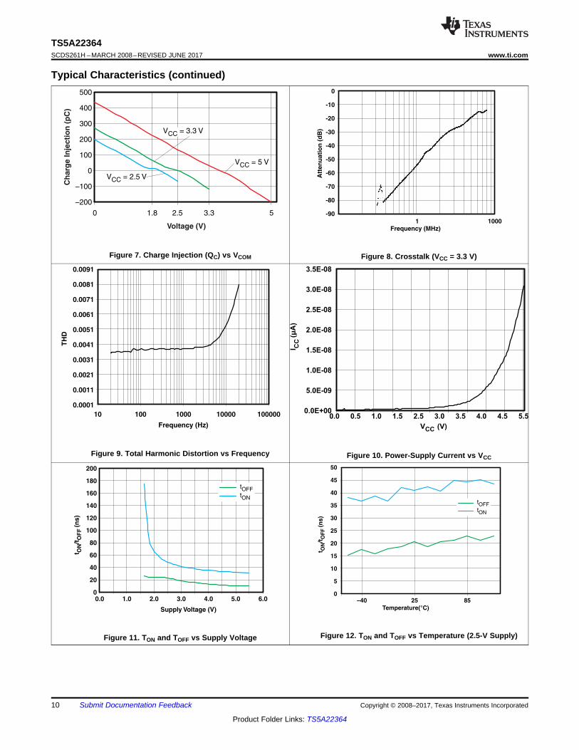
Figure 7. Charge Injection (QC) vs VCOM Figure 8. Crosstalk (VCC = 3.3 V)
Figure 9. Total Harmonic Distortion vs Frequency Figure 10. Power-Supply Current vs VCC
Figure 11. TON and TOFF vs Supply Voltage Figure 12. TON and TOFF vs Temperature (2.5-V Supply)

IN
++
VCC
On-state leakage current
Channel On
VIN = VIH or VIL
IN
IN
+
++
Off-State leakage current
Channel Off
VIN = VIH or VIL
VCC
IN
IN
++
VCC
R-
IN
Ω
11
TS5A22364www.ti.com SCDS261H –MARCH 2008–REVISED JUNE 2017
Product Folder Links: TS5A22364
Submit Documentation FeedbackCopyright © 2008–2017, Texas Instruments Incorporated
7 Parameter Measurement Information
Figure 13. ON-State Resistance (Ron)
Figure 14. OFF-State Leakage Current (ICOM(OFF), INO(OFF))
Figure 15. ON-State Leakage Current(ICOM(ON), INO(ON))

RL CL
tON
tON
90%Switch
Output
(VNO)
Logic
Input
(VIN)
TEST
OFF
tOFF
300 Ω
300 Ω
35 pF
35 pF
IN
VCC
VCC
VCC
VCC
VCOM
90%
IN
COM
BIAS
VNOCapacitance
Meter VBIAS = VCC or GND and
VIN = VIH or VIL
Capacitance is measured at NO,
COM, and IN inputs during ON
and OFF conditions.
VCC
COM
NO
IN
12
TS5A22364SCDS261H –MARCH 2008–REVISED JUNE 2017 www.ti.com
Product Folder Links: TS5A22364
Submit Documentation Feedback Copyright © 2008–2017, Texas Instruments Incorporated
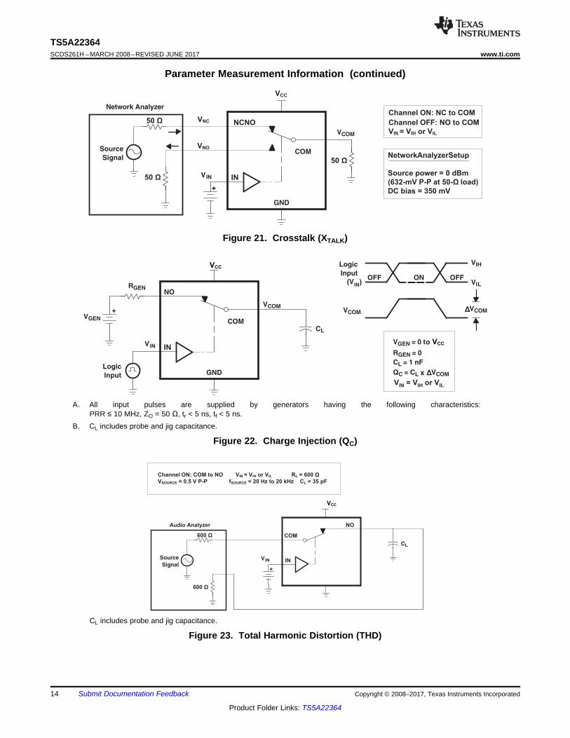
Parameter Measurement Information (continued)
Figure 16. Capacitance(CI, CCOM(OFF), CCOM(ON), CNO(OFF), CNO(ON))
A. All input pulses are supplied by generators having the following characteristics:PRR ≤ 10 MHz, ZO = 50 Ω, tr < 5 ns, tf < 5 ns.
B. CL includes probe and jig capacitance.
Figure 17. Turnon (tON) and Turnoff Time (tOFF)

NetworkAnalyzerSetup
Source power = 0 dBm
(632-mV P-P at 50- loadΩ )
DC bias = 350 mV
Channel OFF: NO to COM
VIN = VIH or VIL50 Ω
IN
+50 Ω
VCC
IN
Network Analyzer Setup
Source power = 0 dBm
(632-mV P-P at 50- load)Ω
DC Bias=350 mV
Channel ON:NO to COM
VIN = VIH or VIL50 Ω
IN
+50 Ω
VCC
IN
VOHNC or NO
VNC
or
VNO
VNC or VNO = GND
RL = 1 kΩ
RPU = 100 Ω
CL = 35 pF
RPU
10%
VCC
VCC
VCC
NC or NO
10%
IN
IN
13
TS5A22364www.ti.com SCDS261H –MARCH 2008–REVISED JUNE 2017
Product Folder Links: TS5A22364
Submit Documentation FeedbackCopyright © 2008–2017, Texas Instruments Incorporated
Parameter Measurement Information (continued)
A. CL includes probe and jig capacitance.B. All input pulses are supplied by generators having the following characteristics:
PRR ≤ 10 MHz, ZO = 50 Ω, tr < 5 ns, tf < 5 ns.
Figure 18. Break-Before-Make Time (tBBM)
Figure 19. Bandwidth (BW)
Figure 20. OFF Isolation (OISO)
Audio Analyzer
600 Ω COM
IN
+
Channel ON: COM to NO VIN = VIH or VIL RL = 600 Ω
VSOURCE = 0.5 V P-P fSOURCE = 20 Hz to 20 kHz CL = 35 pF
600 Ω
VCC
NO
IN
x Δ
Δ
IN
VCC
VCC
IN)
IN
V = V or VIN IH IL
NetworkAnalyzerSetup
Source power = 0 dBm
(632-mV P-P at 50- load)Ω
DC bias = 350 mV
Channel ON: NC to COM
Channel OFF: NO to COM
VIN = VIH or VIL
50 Ω NCNOVNC
IN
+
50 Ω
VNO
VCC
50 Ω
IN
14
TS5A22364SCDS261H –MARCH 2008–REVISED JUNE 2017 www.ti.com
Product Folder Links: TS5A22364
Submit Documentation Feedback Copyright © 2008–2017, Texas Instruments Incorporated
Parameter Measurement Information (continued)
Figure 21. Crosstalk (XTALK)
A. All input pulses are supplied by generators having the following characteristics:PRR ≤ 10 MHz, ZO = 50 Ω, tr < 5 ns, tf < 5 ns.
B. CL includes probe and jig capacitance.
Figure 22. Charge Injection (QC)
CL includes probe and jig capacitance.
Figure 23. Total Harmonic Distortion (THD)

Input Select
ShuntSwitch
IN2
IN1
COM2
COM1
NC2
NC1
NO2
OUT+
OUT+
OUT–
OUT–
NO1
TS5A22364
AudioSource 1
AudioSource 2
8- SpeakerΩ
15
TS5A22364www.ti.com SCDS261H –MARCH 2008–REVISED JUNE 2017
Product Folder Links: TS5A22364
Submit Documentation FeedbackCopyright © 2008–2017, Texas Instruments Incorporated
8 Detailed Description
8.1 OverviewThe TS5A22364 is a bidirectional 2-channel, single-pole, double-throw (SPDT) analog switch designed tooperate from 2.3-V to 5.5-V power supply. The device features negative signal swing capability that allowssignals below ground to pass through the switch without distortion. Additionally, the TS5A22364 includes aninternal shunt switch, which automatically discharges any capacitance at the NC or NO terminals when they arenot connected to COM. Discharging the capacitance reduces the audible click and pop noise when switchingbetween two sources. The break-before-make feature prevents signal distortion during the transferring of a signalfrom one path to another. Low ON-state resistance, excellent channel-to-channel ON-state resistance matching,and minimal total harmonic distortion (THD) performance are ideal for audio applications.
8.2 Functional Block Diagram

16
TS5A22364SCDS261H –MARCH 2008–REVISED JUNE 2017 www.ti.com
Product Folder Links: TS5A22364
Submit Documentation Feedback Copyright © 2008–2017, Texas Instruments Incorporated
8.3 Feature Description
8.3.1 Click and Pop ReductionThe shunt resistors in the TS5A22364 automatically discharge any capacitance at the NC or NO terminals whenthey are not connected to COM. This reduces the audible click-and-pop sounds that occur when switchingbetween audio sources. Audible clicks and pops are caused when a step DC voltage is switched into thespeaker. By automatically discharging the side that is not connected, any residual DC voltage is removed,thereby reducing the clicks and pops.
8.3.2 Negative Signal Swing CapabilityThe TS5A22364 2-channel SPDT switch features negative signal capability that allows signals below ground topass through without distortion. These analog switches operate from a single 2.3-V to 5.5-V supply. The inputand output signal swing of the device is dependant of the supply voltage VCC. The device passes signals as highas VCC and as low as VCC – 5.5 V, including signals below ground with minimal distortion. The OFF state signalpath (either NC or NO) during the operation of TS5A22364 cannot handle negative DC voltage
Table 1 shows the input/output signal swing the user can get with different supply voltages.
Table 1. Input/Output Signal Swing
SUPPLY VOLTAGE, VCC
MINIMUMVNC, VNO, VCOM = VCC - 5.5 V
MAXIMUMVNC, VNO, VCOM = VCC
ON-STATE SIGNAL PATH5.5 V 0 V 5.5 V4.5 V –1.0 V 4.5 V3.6 V –1.9 V 3.6 V3.0 V –2.5 V 3.0 V2.7 V –2.8 V 2.7 V2.3 V -3.2 V 2.3 V
8.4 Device Functional ModesThe function table for TS5A22364 is shown in Table 2.
Table 2. Function Table
IN NC TO COM,COM TO NC
NO TO COM,COM TO NO
L ON OFFH OFF ON
Input Select
ShuntSwitch
IN2
IN1
COM2
COM1
NC2
NC1
NO2
OUT+
OUT+
OUT–
OUT–
NO1
TS5A22364
AudioSource 1
AudioSource 2
8- SpeakerΩ
17
TS5A22364www.ti.com SCDS261H –MARCH 2008–REVISED JUNE 2017
Product Folder Links: TS5A22364
Submit Documentation FeedbackCopyright © 2008–2017, Texas Instruments Incorporated
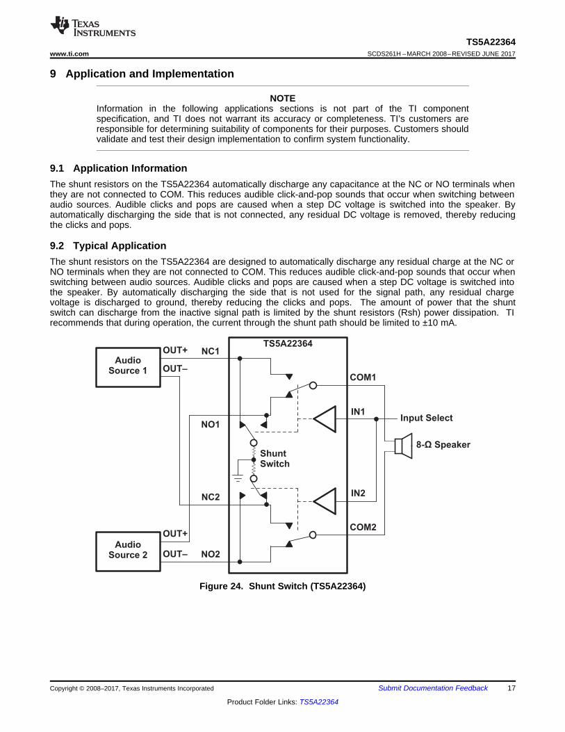
9 Application and Implementation
NOTEInformation in the following applications sections is not part of the TI componentspecification, and TI does not warrant its accuracy or completeness. TI’s customers areresponsible for determining suitability of components for their purposes. Customers shouldvalidate and test their design implementation to confirm system functionality.
9.1 Application InformationThe shunt resistors on the TS5A22364 automatically discharge any capacitance at the NC or NO terminals whenthey are not connected to COM. This reduces audible click-and-pop sounds that occur when switching betweenaudio sources. Audible clicks and pops are caused when a step DC voltage is switched into the speaker. Byautomatically discharging the side that is not connected, any residual DC voltage is removed, thereby reducingthe clicks and pops.
9.2 Typical ApplicationThe shunt resistors on the TS5A22364 are designed to automatically discharge any residual charge at the NC orNO terminals when they are not connected to COM. This reduces audible click-and-pop sounds that occur whenswitching between audio sources. Audible clicks and pops are caused when a step DC voltage is switched intothe speaker. By automatically discharging the side that is not used for the signal path, any residual chargevoltage is discharged to ground, thereby reducing the clicks and pops. The amount of power that the shuntswitch can discharge from the inactive signal path is limited by the shunt resistors (Rsh) power dissipation. TIrecommends that during operation, the current through the shunt path should be limited to ±10 mA.
Figure 24. Shunt Switch (TS5A22364)

VCOM (V)
Ro
n
)
VCC = 2.3 V
VCC = 3.0 V
VCC = 4.5 V
1.2
1.0
0.8
0.6
0.4
0.2
0.0
-4.0 -2.0 2.00.0 4.0 6.0
18
TS5A22364SCDS261H –MARCH 2008–REVISED JUNE 2017 www.ti.com
Product Folder Links: TS5A22364
Submit Documentation Feedback Copyright © 2008–2017, Texas Instruments Incorporated
Typical Application (continued)9.2.1 Design RequirementsTie the digitally controlled inputs select pins IN1 and IN2 to VCC or GND to avoid unwanted switch states andhigh current consumption that could result if the logic control pins are left floating.
9.2.2 Detailed Design ProcedureSelect the appropriate supply voltage to cover the entire voltage swing of the signal passing through the switchbecause the TS5A22364 operates from a single 2.3-V to 5.5-V supply and the input and output signal swing ofthe device is dependant of the supply voltage, VCC. The device will pass signals as high as VCC and as low asVCC – 5.5 V. Use Table 1 as a guide for selecting supply voltage based on the signal passing through the ON-state switch path.
Ensure that the device is powered up with a valid supply voltage on VCC before a voltage can be applied to thesignal paths NC and NO.
9.2.3 Application Curve
Figure 25. Ron vs VCOM

1
2
3
4
LEGEND
VIA to Power Plane
9
8
7
Bypass Capacitor
VCC
6
To System
To System
To System
To System
To System
To System
To System
NC1
IN15 GND
IN2
NC2
COM2
NO2 10
COM1
NO1
VCC
VIA to GND
Polygonal Copper Pour
To System
19
TS5A22364www.ti.com SCDS261H –MARCH 2008–REVISED JUNE 2017
Product Folder Links: TS5A22364
Submit Documentation FeedbackCopyright © 2008–2017, Texas Instruments Incorporated
10 Power Supply RecommendationsThe TS5A22364 operates from a single 2.3-V to 5.5-V supply. The device must be powered up with a supplyvoltage on VCC before a voltage can be applied to the signal paths NC and NO. TI recommends to include a100-μs delay after VCC is at voltage before applying a signal on NC and NO paths
It is also good practice to place a 0.1-μF bypass capacitor on the supply pin VCC to GND to smooth out lowerfrequency noise to provide better load regulation across the frequency spectrum.
11 Layout
11.1 Layout GuidelinesTI recommends placing a bypass capacitor as close to the supply pin VCC as possible to help smooth out lowerfrequency noise to provide better load regulation across the frequency spectrum.
Minimize trace lengths and vias on the signal paths in order to preserve signal integrity.
11.2 Layout Example
Figure 26. Layout Example of TS5A22364

20
TS5A22364SCDS261H –MARCH 2008–REVISED JUNE 2017 www.ti.com
Product Folder Links: TS5A22364
Submit Documentation Feedback Copyright © 2008–2017, Texas Instruments Incorporated
12 Device and Documentation Support
12.1 Receiving Notification of Documentation UpdatesTo receive notification of documentation updates, navigate to the device product folder on ti.com. In the upperright corner, click on Alert me to register and receive a weekly digest of any product information that haschanged. For change details, review the revision history included in any revised document.
12.2 Community ResourcesThe following links connect to TI community resources. Linked contents are provided "AS IS" by the respectivecontributors. They do not constitute TI specifications and do not necessarily reflect TI's views; see TI's Terms ofUse.
TI E2E™ Online Community TI's Engineer-to-Engineer (E2E) Community. Created to foster collaborationamong engineers. At e2e.ti.com, you can ask questions, share knowledge, explore ideas and helpsolve problems with fellow engineers.
Design Support TI's Design Support Quickly find helpful E2E forums along with design support tools andcontact information for technical support.
12.3 TrademarksE2E is a trademark of Texas Instruments.All other trademarks are the property of their respective owners.
12.4 Electrostatic Discharge CautionThese devices have limited built-in ESD protection. The leads should be shorted together or the device placed in conductive foamduring storage or handling to prevent electrostatic damage to the MOS gates.
12.5 GlossarySLYZ022 — TI Glossary.
This glossary lists and explains terms, acronyms, and definitions.
13 Mechanical, Packaging, and Orderable InformationThe following pages include mechanical, packaging, and orderable information. This information is the mostcurrent data available for the designated devices. This data is subject to change without notice and revision ofthis document. For browser-based versions of this data sheet, refer to the left-hand navigation.

PACKAGE OPTION ADDENDUM
www.ti.com 19-Jun-2017
Addendum-Page 1
PACKAGING INFORMATION
Orderable Device Status(1)
Package Type PackageDrawing
Pins PackageQty
Eco Plan(2)
Lead/Ball Finish(6)
MSL Peak Temp(3)
Op Temp (°C) Device Marking(4/5)
Samples
TS5A22364DGSR ACTIVE VSSOP DGS 10 2500 Green (RoHS& no Sb/Br)
CU NIPDAU Level-1-260C-UNLIM -40 to 85 (38Q ~ 38R)
TS5A22364DGSRG4 ACTIVE VSSOP DGS 10 2500 Green (RoHS& no Sb/Br)
CU NIPDAU Level-1-260C-UNLIM -40 to 85 (38Q ~ 38R)
TS5A22364DRCR ACTIVE VSON DRC 10 3000 Green (RoHS& no Sb/Br)
CU NIPDAU Level-2-260C-1 YEAR -40 to 85 ZVF
TS5A22364YZPR ACTIVE DSBGA YZP 10 3000 Green (RoHS& no Sb/Br)
SNAGCU Level-1-260C-UNLIM -40 to 85 (38 ~ 382)
(1) The marketing status values are defined as follows:ACTIVE: Product device recommended for new designs.LIFEBUY: TI has announced that the device will be discontinued, and a lifetime-buy period is in effect.NRND: Not recommended for new designs. Device is in production to support existing customers, but TI does not recommend using this part in a new design.PREVIEW: Device has been announced but is not in production. Samples may or may not be available.OBSOLETE: TI has discontinued the production of the device.
(2) RoHS: TI defines "RoHS" to mean semiconductor products that are compliant with the current EU RoHS requirements for all 10 RoHS substances, including the requirement that RoHS substancedo not exceed 0.1% by weight in homogeneous materials. Where designed to be soldered at high temperatures, "RoHS" products are suitable for use in specified lead-free processes. TI mayreference these types of products as "Pb-Free".RoHS Exempt: TI defines "RoHS Exempt" to mean products that contain lead but are compliant with EU RoHS pursuant to a specific EU RoHS exemption.Green: TI defines "Green" to mean the content of Chlorine (Cl) and Bromine (Br) based flame retardants meet JS709B low halogen requirements of <=1000ppm threshold. Antimony trioxide basedflame retardants must also meet the <=1000ppm threshold requirement.
(3) MSL, Peak Temp. - The Moisture Sensitivity Level rating according to the JEDEC industry standard classifications, and peak solder temperature.
(4) There may be additional marking, which relates to the logo, the lot trace code information, or the environmental category on the device.
(5) Multiple Device Markings will be inside parentheses. Only one Device Marking contained in parentheses and separated by a "~" will appear on a device. If a line is indented then it is a continuationof the previous line and the two combined represent the entire Device Marking for that device.
(6) Lead/Ball Finish - Orderable Devices may have multiple material finish options. Finish options are separated by a vertical ruled line. Lead/Ball Finish values may wrap to two lines if the finishvalue exceeds the maximum column width.
Important Information and Disclaimer:The information provided on this page represents TI's knowledge and belief as of the date that it is provided. TI bases its knowledge and belief on informationprovided by third parties, and makes no representation or warranty as to the accuracy of such information. Efforts are underway to better integrate information from third parties. TI has taken and

PACKAGE OPTION ADDENDUM
www.ti.com 19-Jun-2017
Addendum-Page 2
continues to take reasonable steps to provide representative and accurate information but may not have conducted destructive testing or chemical analysis on incoming materials and chemicals.TI and TI suppliers consider certain information to be proprietary, and thus CAS numbers and other limited information may not be available for release.
In no event shall TI's liability arising out of such information exceed the total purchase price of the TI part(s) at issue in this document sold by TI to Customer on an annual basis.
OTHER QUALIFIED VERSIONS OF TS5A22364 :
• Automotive: TS5A22364-Q1
NOTE: Qualified Version Definitions:
• Automotive - Q100 devices qualified for high-reliability automotive applications targeting zero defects

TAPE AND REEL INFORMATION
*All dimensions are nominal
Device PackageType
PackageDrawing
Pins SPQ ReelDiameter
(mm)
ReelWidth
W1 (mm)
A0(mm)
B0(mm)
K0(mm)
P1(mm)
W(mm)
Pin1Quadrant
TS5A22364DGSR VSSOP DGS 10 2500 330.0 12.4 5.3 3.4 1.4 8.0 12.0 Q1
TS5A22364DRCR VSON DRC 10 3000 330.0 12.4 3.3 3.3 1.1 8.0 12.0 Q2
TS5A22364YZPR DSBGA YZP 10 3000 178.0 9.2 1.49 1.99 0.63 4.0 8.0 Q2
PACKAGE MATERIALS INFORMATION
www.ti.com 3-Aug-2017
Pack Materials-Page 1

*All dimensions are nominal
Device Package Type Package Drawing Pins SPQ Length (mm) Width (mm) Height (mm)
TS5A22364DGSR VSSOP DGS 10 2500 358.0 335.0 35.0
TS5A22364DRCR VSON DRC 10 3000 367.0 367.0 35.0
TS5A22364YZPR DSBGA YZP 10 3000 220.0 220.0 35.0
PACKAGE MATERIALS INFORMATION
www.ti.com 3-Aug-2017
Pack Materials-Page 2

www.ti.com
PACKAGE OUTLINE
C0.5 MAX
0.190.15
1.5TYP
1 TYP
0.5TYP
0.5 TYP10X 0.25
0.21
B E A
D
DSBGA - 0.5 mm max heightYZP0010DIE SIZE BALL GRID ARRAY
4219350/B 11/2017
NOTES: 1. All linear dimensions are in millimeters. Any dimensions in parenthesis are for reference only. Dimensioning and tolerancing per ASME Y14.5M.2. This drawing is subject to change without notice.
BALL A3CORNER
SEATING PLANE
BALL TYP 0.015 C
D
C
B
A
1 2 3
0.015 C A B
SYMM
SYMM
SCALE 8.000
D: Max =
E: Max =
1.89 mm, Min =
1.39 mm, Min =
1.83 mm
1.33 mm

www.ti.com
EXAMPLE BOARD LAYOUT
10X ( 0.225)(0.5) TYP
(0.5) TYP
( 0.225)METAL
0.05 MAX
SOLDER MASKOPENING
METALUNDERMASK
( 0.225)SOLDER MASKOPENING
0.05 MIN
DSBGA - 0.5 mm max heightYZP0010DIE SIZE BALL GRID ARRAY
4219350/B 11/2017
NOTES: (continued) 3. Final dimensions may vary due to manufacturing tolerance considerations and also routing constraints. For more information, see Texas Instruments literature number SBVA017 (www.ti.com/lit/sbva017).
1
SYMM
SYMM
LAND PATTERN EXAMPLESCALE:30X
D
C
2 3
A
B
NON-SOLDER MASKDEFINED
(PREFERRED)
SOLDER MASK DETAILSNOT TO SCALE
SOLDER MASKDEFINED

www.ti.com
EXAMPLE STENCIL DESIGN
(0.5)TYP
(0.5) TYP
10X ( 0.25) (R0.05) TYP
METALTYP
DSBGA - 0.5 mm max heightYZP0010DIE SIZE BALL GRID ARRAY
4219350/B 11/2017
NOTES: (continued) 4. Laser cutting apertures with trapezoidal walls and rounded corners may offer better paste release.
D
C
1 2 3
A
B
SYMM
SYMM
SOLDER PASTE EXAMPLEBASED ON 0.1 mm THICK STENCIL
SCALE:30X


GENERIC PACKAGE VIEW
Images above are just a representation of the package family, actual package may vary.Refer to the product data sheet for package details.
DRC 10 VSON - 1 mm max heightPLASTIC SMALL OUTLINE - NO LEAD
4204102-3/M

www.ti.com
PACKAGE OUTLINE
C
10X 0.300.18
2.4 0.1
2X2
1.65 0.1
8X 0.5
1 MAX
10X 0.50.3
0.050.00
A 3.12.9
B
3.12.9
(0.2) TYP4X (0.25)
2X (0.5)
VSON - 1 mm max heightDRC0010JPLASTIC SMALL OUTLINE - NO LEAD
4218878/A 09/2017
PIN 1 INDEX AREA
SEATING PLANE
0.08 C
1
56
10
(OPTIONAL)PIN 1 ID 0.1 C A B
0.05 C
THERMAL PADEXPOSED
SYMM
SYMM11
NOTES: 1. All linear dimensions are in millimeters. Any dimensions in parenthesis are for reference only. Dimensioning and tolerancing per ASME Y14.5M. 2. This drawing is subject to change without notice. 3. The package thermal pad must be soldered to the printed circuit board for optimal thermal and mechanical performance.
SCALE 4.000
www.ti.com
EXAMPLE BOARD LAYOUT
0.07 MINALL AROUND
10X (0.25)
(2.4)
(2.8)
8X (0.5)
(1.65)
( 0.2) VIATYP
(0.575)
(0.95)
10X (0.6)
(R0.05) TYP
(3.4)
4X (0.25)
(0.5)
VSON - 1 mm max heightDRC0010JPLASTIC SMALL OUTLINE - NO LEAD
4218878/A 09/2017
SYMM
1
5 6
10
LAND PATTERN EXAMPLEEXPOSED METAL SHOWN
SCALE:20X
11SYMM
METAL UNDERSOLDER MASK
SOLDER MASKOPENING
NOTES: (continued) 4. This package is designed to be soldered to a thermal pad on the board. For more information, see Texas Instruments literature number SLUA271 (www.ti.com/lit/slua271).5. Vias are optional depending on application, refer to device data sheet. If any vias are implemented, refer to their locations shown on this view. It is recommended that vias under paste be filled, plugged or tented.

www.ti.com
EXAMPLE STENCIL DESIGN
(R0.05) TYP
10X (0.25)
10X (0.6)
2X (1.5)
2X(1.06)
(2.8)
(0.63)
8X (0.5)
(0.5)
4X (0.34)
4X (0.25)
(1.53)
VSON - 1 mm max heightDRC0010JPLASTIC SMALL OUTLINE - NO LEAD
4218878/A 09/2017
NOTES: (continued) 6. Laser cutting apertures with trapezoidal walls and rounded corners may offer better paste release. IPC-7525 may have alternate design recommendations.
SOLDER PASTE EXAMPLEBASED ON 0.125 mm THICK STENCIL
EXPOSED PAD 11:
80% PRINTED SOLDER COVERAGE BY AREASCALE:25X
SYMM
1
56
10
EXPOSED METALTYP
11
SYMM
SOLDER MASK OPENING
METAL UNDERSOLDER MASK

IMPORTANT NOTICE
Texas Instruments Incorporated (TI) reserves the right to make corrections, enhancements, improvements and other changes to itssemiconductor products and services per JESD46, latest issue, and to discontinue any product or service per JESD48, latest issue. Buyersshould obtain the latest relevant information before placing orders and should verify that such information is current and complete.TI’s published terms of sale for semiconductor products (http://www.ti.com/sc/docs/stdterms.htm) apply to the sale of packaged integratedcircuit products that TI has qualified and released to market. Additional terms may apply to the use or sale of other types of TI products andservices.Reproduction of significant portions of TI information in TI data sheets is permissible only if reproduction is without alteration and isaccompanied by all associated warranties, conditions, limitations, and notices. TI is not responsible or liable for such reproduceddocumentation. Information of third parties may be subject to additional restrictions. Resale of TI products or services with statementsdifferent from or beyond the parameters stated by TI for that product or service voids all express and any implied warranties for theassociated TI product or service and is an unfair and deceptive business practice. TI is not responsible or liable for any such statements.Buyers and others who are developing systems that incorporate TI products (collectively, “Designers”) understand and agree that Designersremain responsible for using their independent analysis, evaluation and judgment in designing their applications and that Designers havefull and exclusive responsibility to assure the safety of Designers' applications and compliance of their applications (and of all TI productsused in or for Designers’ applications) with all applicable regulations, laws and other applicable requirements. Designer represents that, withrespect to their applications, Designer has all the necessary expertise to create and implement safeguards that (1) anticipate dangerousconsequences of failures, (2) monitor failures and their consequences, and (3) lessen the likelihood of failures that might cause harm andtake appropriate actions. Designer agrees that prior to using or distributing any applications that include TI products, Designer willthoroughly test such applications and the functionality of such TI products as used in such applications.TI’s provision of technical, application or other design advice, quality characterization, reliability data or other services or information,including, but not limited to, reference designs and materials relating to evaluation modules, (collectively, “TI Resources”) are intended toassist designers who are developing applications that incorporate TI products; by downloading, accessing or using TI Resources in anyway, Designer (individually or, if Designer is acting on behalf of a company, Designer’s company) agrees to use any particular TI Resourcesolely for this purpose and subject to the terms of this Notice.TI’s provision of TI Resources does not expand or otherwise alter TI’s applicable published warranties or warranty disclaimers for TIproducts, and no additional obligations or liabilities arise from TI providing such TI Resources. TI reserves the right to make corrections,enhancements, improvements and other changes to its TI Resources. TI has not conducted any testing other than that specificallydescribed in the published documentation for a particular TI Resource.Designer is authorized to use, copy and modify any individual TI Resource only in connection with the development of applications thatinclude the TI product(s) identified in such TI Resource. NO OTHER LICENSE, EXPRESS OR IMPLIED, BY ESTOPPEL OR OTHERWISETO ANY OTHER TI INTELLECTUAL PROPERTY RIGHT, AND NO LICENSE TO ANY TECHNOLOGY OR INTELLECTUAL PROPERTYRIGHT OF TI OR ANY THIRD PARTY IS GRANTED HEREIN, including but not limited to any patent right, copyright, mask work right, orother intellectual property right relating to any combination, machine, or process in which TI products or services are used. Informationregarding or referencing third-party products or services does not constitute a license to use such products or services, or a warranty orendorsement thereof. Use of TI Resources may require a license from a third party under the patents or other intellectual property of thethird party, or a license from TI under the patents or other intellectual property of TI.TI RESOURCES ARE PROVIDED “AS IS” AND WITH ALL FAULTS. TI DISCLAIMS ALL OTHER WARRANTIES ORREPRESENTATIONS, EXPRESS OR IMPLIED, REGARDING RESOURCES OR USE THEREOF, INCLUDING BUT NOT LIMITED TOACCURACY OR COMPLETENESS, TITLE, ANY EPIDEMIC FAILURE WARRANTY AND ANY IMPLIED WARRANTIES OFMERCHANTABILITY, FITNESS FOR A PARTICULAR PURPOSE, AND NON-INFRINGEMENT OF ANY THIRD PARTY INTELLECTUALPROPERTY RIGHTS. TI SHALL NOT BE LIABLE FOR AND SHALL NOT DEFEND OR INDEMNIFY DESIGNER AGAINST ANY CLAIM,INCLUDING BUT NOT LIMITED TO ANY INFRINGEMENT CLAIM THAT RELATES TO OR IS BASED ON ANY COMBINATION OFPRODUCTS EVEN IF DESCRIBED IN TI RESOURCES OR OTHERWISE. IN NO EVENT SHALL TI BE LIABLE FOR ANY ACTUAL,DIRECT, SPECIAL, COLLATERAL, INDIRECT, PUNITIVE, INCIDENTAL, CONSEQUENTIAL OR EXEMPLARY DAMAGES INCONNECTION WITH OR ARISING OUT OF TI RESOURCES OR USE THEREOF, AND REGARDLESS OF WHETHER TI HAS BEENADVISED OF THE POSSIBILITY OF SUCH DAMAGES.Unless TI has explicitly designated an individual product as meeting the requirements of a particular industry standard (e.g., ISO/TS 16949and ISO 26262), TI is not responsible for any failure to meet such industry standard requirements.Where TI specifically promotes products as facilitating functional safety or as compliant with industry functional safety standards, suchproducts are intended to help enable customers to design and create their own applications that meet applicable functional safety standardsand requirements. Using products in an application does not by itself establish any safety features in the application. Designers mustensure compliance with safety-related requirements and standards applicable to their applications. Designer may not use any TI products inlife-critical medical equipment unless authorized officers of the parties have executed a special contract specifically governing such use.Life-critical medical equipment is medical equipment where failure of such equipment would cause serious bodily injury or death (e.g., lifesupport, pacemakers, defibrillators, heart pumps, neurostimulators, and implantables). Such equipment includes, without limitation, allmedical devices identified by the U.S. Food and Drug Administration as Class III devices and equivalent classifications outside the U.S.TI may expressly designate certain products as completing a particular qualification (e.g., Q100, Military Grade, or Enhanced Product).Designers agree that it has the necessary expertise to select the product with the appropriate qualification designation for their applicationsand that proper product selection is at Designers’ own risk. Designers are solely responsible for compliance with all legal and regulatoryrequirements in connection with such selection.Designer will fully indemnify TI and its representatives against any damages, costs, losses, and/or liabilities arising out of Designer’s non-compliance with the terms and provisions of this Notice.
Mailing Address: Texas Instruments, Post Office Box 655303, Dallas, Texas 75265Copyright © 2018, Texas Instruments Incorporated