trs3238e 3-vto 5.5-vmultichannel rs-232line … sheets/texas instruments pdfs... · din2 din3 rout1...
TRANSCRIPT
www.ti.com
FEATURES
APPLICATIONSDOUT1
DOUT2
DOUT3
RIN1
RIN2
DOUT4
RIN3
N.C.
C1–
DIN1
DIN2
DIN3
ROUT1
ROUT2
DIN4
ROUT3
1
2
3
4
5
6
7
8
9
10
11
12
13
14
28
27
26
25
24
23
22
21
20
19
18
17
16
15
C2+
GND
C2-
V-
DOUT1
DOUT2
DOUT3
RIN1
RIN2
DOUT4
RIN3
DOUT5
FORCEON
FORCEOFF
C1+
V+
VCC
C1-
DIN1
DIN2
DIN3
ROUT1
ROUT2
DIN4
ROUT3
DIN5
ROUT1B
INVALID
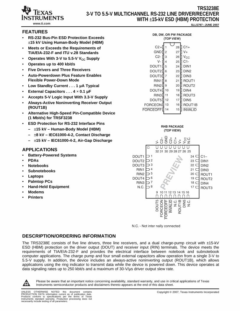
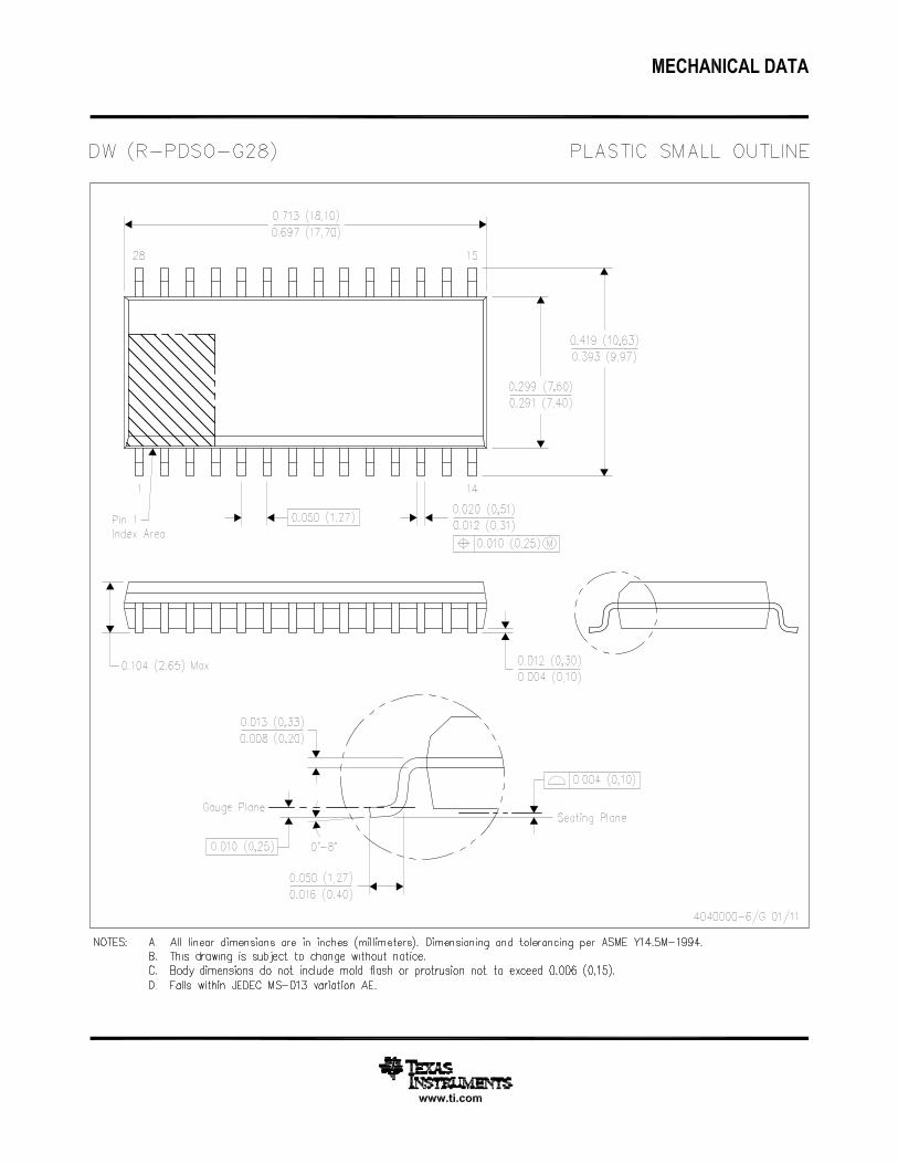
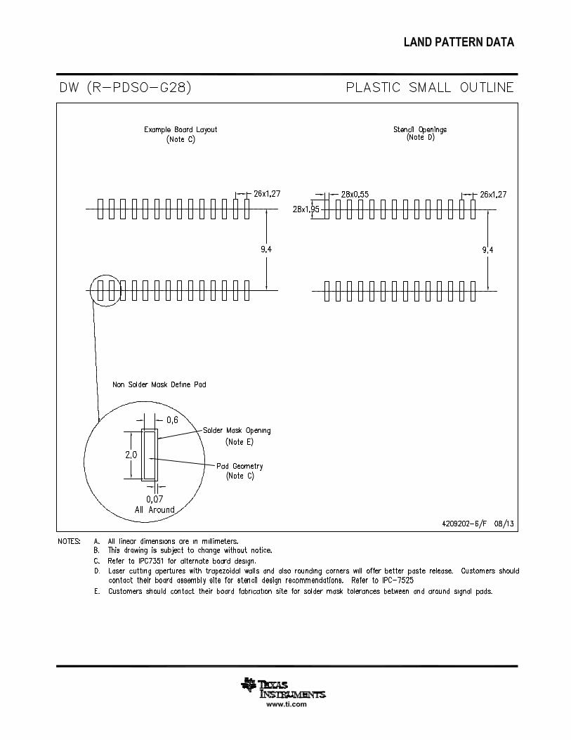
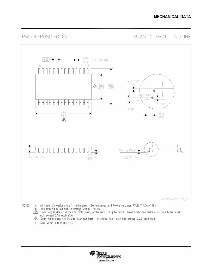
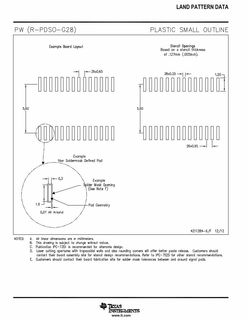
DB, DW, OR PW PACKAGE
(TOP VIEW)
RHB PACKAGE
(TOP VIEW)
V-
C2–
GN
D
C2+
C1+
V+
VC
C
N.C
.
DO
UT
5
FO
RC
EO
N
FO
RC
EO
FF
INV
ALID
N.C
.
RO
UT
1B
DIN
5
N.C
.
1
2
3
4
5
6
7
8
24
23
22
21
20
19
18
17
3132 30 29 28 27 26 25
109 11 12 13 14 15 16
N.C. - Not inter nally connected
DESCRIPTION/ORDERING INFORMATION
TRS3238E3-V TO 5.5-V MULTICHANNEL RS-232 LINE DRIVER/RECEIVER
WITH ±15-kV ESD (HBM) PROTECTIONSLLS797–JUNE 2007
• RS-232 Bus-Pin ESD Protection Exceeds±15 kV Using Human-Body Model (HBM)
• Meets or Exceeds the Requirements ofTIA/EIA-232-F and ITU v.28 Standards
• Operates With 3-V to 5.5-V VCC Supply• Operates up to 400 kbit/s• Five Drivers and Three Receivers• Auto-Powerdown Plus Feature Enables
Flexible Power-Down Mode• Low Standby Current . . . 1 μA Typical• External Capacitors . . . 4 × 0.1 μF• Accepts 5-V Logic Input With 3.3-V Supply• Always-Active Noninverting Receiver Output
(ROUT1B)• Alternative High-Speed Pin-Compatible Device
(1 Mbit/s) for TRSF3238• ESD Protection for RS-232 Interface Pins
– ±15 kV – Human-Body Model (HBM)– ±8 kV – IEC61000-4-2, Contact Discharge– ±15 kV – IEC61000-4-2, Air-Gap Discharge
• Battery-Powered Systems• PDAs• Notebooks• Subnotebooks• Laptops• Palmtop PCs• Hand-Held Equipment• Modems• Printers
The TRS3238E consists of five line drivers, three line receivers, and a dual charge-pump circuit with ±15-kVESD (HBM) protection on the driver output (DOUT) and receiver input (RIN) terminals. The device meets therequirements of TIA/EIA-232-F and provides the electrical interface between notebook and subnotebookcomputer applications. The charge pump and four small external capacitors allow operation from a single 3-V to5.5-V supply. In addition, the device includes an always-active noninverting output (ROUT1B), which allowsapplications using the ring indicator to transmit data while the device is powered down. This device operates atdata signaling rates up to 250 kbit/s and a maximum of 30-V/μs driver output slew rate.
Please be aware that an important notice concerning availability, standard warranty, and use in critical applications of TexasInstruments semiconductor products and disclaimers thereto appears at the end of this data sheet.
UNLESS OTHERWISE NOTED this document contains Copyright © 2007, Texas Instruments IncorporatedPRODUCTION DATA information current as of publication date.Products conform to specifications per the terms of TexasInstruments standard warranty. Production processing does notnecessarily include testing of all parameters.
www.ti.com
DESCRIPTION/ORDERING INFORMATION (CONTINUED)
TRS3238E3-V TO 5.5-V MULTICHANNEL RS-232 LINE DRIVER/RECEIVERWITH ±15-kV ESD (HBM) PROTECTIONSLLS797–JUNE 2007
Flexible control options for power management are featured when the serial port and driver inputs are inactive.The auto-powerdown plus feature functions when FORCEON is low and FORCEOFF is high. During this modeof operation, if the device does not sense valid signal transitions on all receiver and driver inputs forapproximately 30 s, the built-in charge pump and drivers are powered down, reducing the supply current to1 μA. By disconnecting the serial port or placing the peripheral drivers off, auto-powerdown plus occurs if thereis no activity in the logic levels for the driver inputs. Auto-powerdown plus can be disabled when FORCEON andFORCEOFF are high. With auto-powerdown plus enabled, the device activates automatically when a valid signalis applied to any receiver or driver input. INVALID is high (valid data) if any receiver input voltage is greater than2.7 V or less than –2.7 V, or has been between –0.3 V and 0.3 V for less than 30 μs. INVALID is low (invaliddata) if all receiver input voltages are between –0.3 V and 0.3 V for more than 30 μs. Refer to Figure 5 forreceiver input levels.
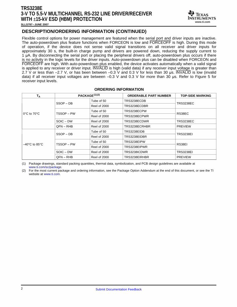
ORDERING INFORMATION
TA PACKAGE (1) (2) ORDERABLE PART NUMBER TOP-SIDE MARKING
Tube of 50 TRS3238ECDBSSOP – DB TRS3238EC
Reel of 2000 TRS3238ECDBR
Tube of 50 TRS3238ECPW0°C to 70°C TSSOP – PW RS38EC
Reel of 2000 TRS3238ECPWR
SOIC – DW Reel of 2000 TRS3238ECDWR TRS3238EC
QFN – RHB Reel of 2000 TRS3238ECRHBR PREVIEW
Tube of 50 TRS3238EIDBSSOP – DB TRS3238EI
Reel of 2000 TRS3238EIDBR
Tube of 50 TRS3238EIPW–40°C to 85°C TSSOP – PW RS38EI
Reel of 2000 TRS3238EIPWR
SOIC – DW Reel of 2000 TRS3238ICDWR TRS3238EI
QFN – RHB Reel of 2000 TRS3238EIRHBR PREVIEW
(1) Package drawings, standard packing quantities, thermal data, symbolization, and PCB design guidelines are available atwww.ti.com/sc/package.
(2) For the most current package and ordering information, see the Package Option Addendum at the end of this document, or see the TIwebsite at www.ti.com.
2 Submit Documentation Feedback
www.ti.com
TRS3238E3-V TO 5.5-V MULTICHANNEL RS-232 LINE DRIVER/RECEIVER
WITH ±15-kV ESD (HBM) PROTECTIONSLLS797–JUNE 2007
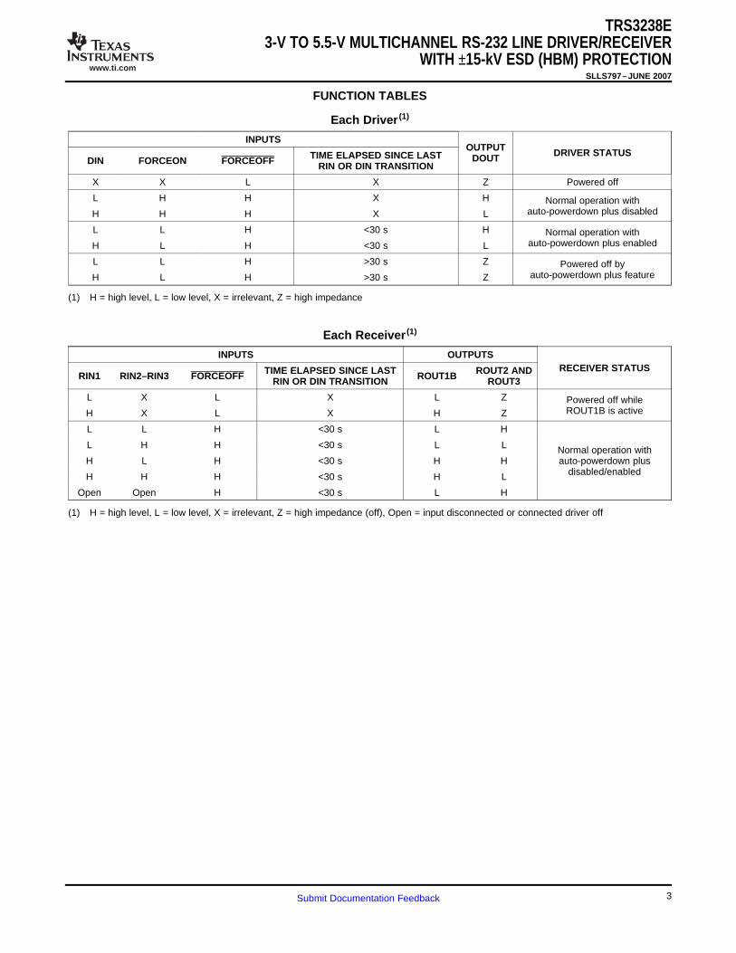
FUNCTION TABLESabc
Each Driver (1)
INPUTSOUTPUT DRIVER STATUSTIME ELAPSED SINCE LAST DOUTDIN FORCEON FORCEOFF RIN OR DIN TRANSITION
X X L X Z Powered off
L H H X H Normal operation withauto-powerdown plus disabledH H H X L
L L H <30 s H Normal operation withauto-powerdown plus enabledH L H <30 s L
L L H >30 s Z Powered off byauto-powerdown plus featureH L H >30 s Z
(1) H = high level, L = low level, X = irrelevant, Z = high impedance
Each Receiver (1)
INPUTS OUTPUTSRECEIVER STATUSTIME ELAPSED SINCE LAST ROUT2 ANDRIN1 RIN2–RIN3 FORCEOFF ROUT1BRIN OR DIN TRANSITION ROUT3
L X L X L Z Powered off whileROUT1B is activeH X L X H Z
L L H <30 s L H
L H H <30 s L L Normal operation withH L H <30 s H H auto-powerdown plus
disabled/enabledH H H <30 s H L
Open Open H <30 s L H
(1) H = high level, L = low level, X = irrelevant, Z = high impedance (off), Open = input disconnected or connected driver off
3Submit Documentation Feedback
www.ti.com
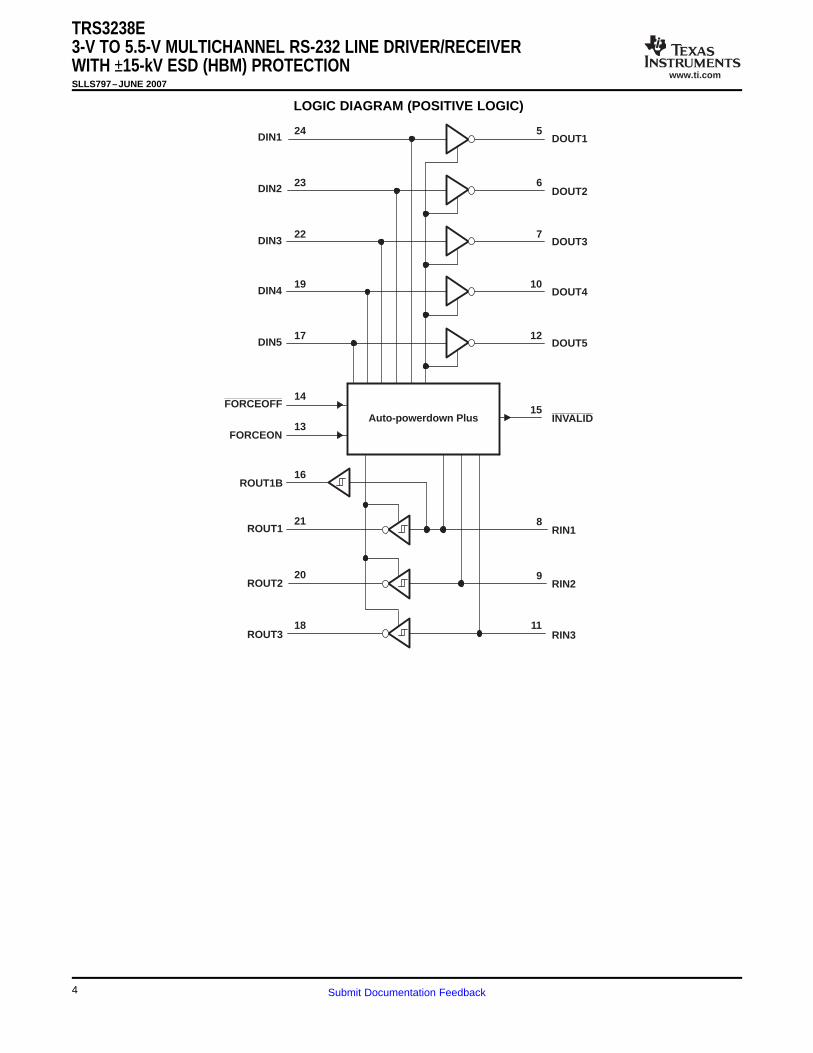
DIN3
DIN2
DIN1
DOUT3
DOUT2
DOUT1
Auto-powerdown Plus INVALID
RIN1
RIN2
RIN3
FORCEOFF
FORCEON
ROUT1
ROUT1B
ROUT2
ROUT3
24
23
22
14
13
21
16
20
18
5
6
7
15
8
9
11
DIN4 DOUT419 10
DIN5 DOUT517 12
TRS3238E3-V TO 5.5-V MULTICHANNEL RS-232 LINE DRIVER/RECEIVERWITH ±15-kV ESD (HBM) PROTECTIONSLLS797–JUNE 2007
LOGIC DIAGRAM (POSITIVE LOGIC)
4 Submit Documentation Feedback
www.ti.com
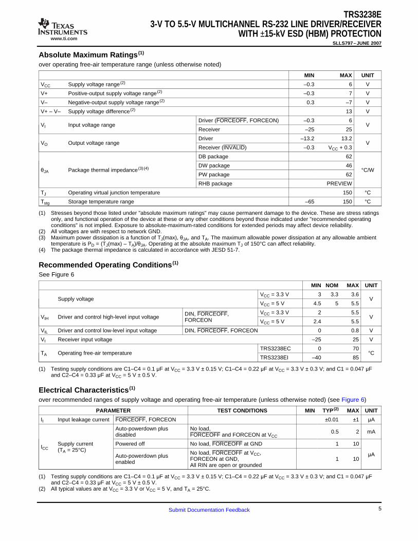
Absolute Maximum Ratings (1)
Recommended Operating Conditions (1)
Electrical Characteristics (1)
TRS3238E3-V TO 5.5-V MULTICHANNEL RS-232 LINE DRIVER/RECEIVER
WITH ±15-kV ESD (HBM) PROTECTIONSLLS797–JUNE 2007
over operating free-air temperature range (unless otherwise noted)
MIN MAX UNIT
VCC Supply voltage range (2) –0.3 6 V
V+ Positive-output supply voltage range (2) –0.3 7 V
V– Negative-output supply voltage range (2) 0.3 –7 V
V+ – V– Supply voltage difference (2) 13 V
Driver (FORCEOFF, FORCEON) –0.3 6VI Input voltage range V
Receiver –25 25
Driver –13.2 13.2VO Output voltage range V
Receiver (INVALID) –0.3 VCC + 0.3
DB package 62
DW package 46θJA Package thermal impedance (3) (4) °C/W
PW package 62
RHB package PREVIEW
TJ Operating virtual junction temperature 150 °C
Tstg Storage temperature range –65 150 °C
(1) Stresses beyond those listed under "absolute maximum ratings" may cause permanent damage to the device. These are stress ratingsonly, and functional operation of the device at these or any other conditions beyond those indicated under "recommended operatingconditions" is not implied. Exposure to absolute-maximum-rated conditions for extended periods may affect device reliability.
(2) All voltages are with respect to network GND.(3) Maximum power dissipation is a function of TJ(max), θJA, and TA. The maximum allowable power dissipation at any allowable ambient
temperature is PD = (TJ(max) – TA)/θJA. Operating at the absolute maximum TJ of 150°C can affect reliability.(4) The package thermal impedance is calculated in accordance with JESD 51-7.
See Figure 6
MIN NOM MAX UNIT
VCC = 3.3 V 3 3.3 3.6Supply voltage V
VCC = 5 V 4.5 5 5.5
VCC = 3.3 V 2 5.5DIN, FORCEOFF,VIH Driver and control high-level input voltage VFORCEON VCC = 5 V 2.4 5.5
VIL Driver and control low-level input voltage DIN, FORCEOFF, FORCEON 0 0.8 V
VI Receiver input voltage –25 25 V
TRS3238EC 0 70TA Operating free-air temperature °C
TRS3238EI –40 85
(1) Testing supply conditions are C1–C4 = 0.1 μF at VCC = 3.3 V ± 0.15 V; C1–C4 = 0.22 μF at VCC = 3.3 V ± 0.3 V; and C1 = 0.047 μFand C2–C4 = 0.33 μF at VCC = 5 V ± 0.5 V.
over recommended ranges of supply voltage and operating free-air temperature (unless otherwise noted) (see Figure 6)
PARAMETER TEST CONDITIONS MIN TYP (2) MAX UNIT
II Input leakage current FORCEOFF, FORCEON ±0.01 ±1 μA
Auto-powerdown plus No load, 0.5 2 mAdisabled FORCEOFF and FORCEON at VCC
Supply current Powered off No load, FORCEOFF at GND 1 10ICC (TA = 25°C) No load, FORCEOFF at VCC, μAAuto-powerdown plus FORCEON at GND, 1 10enabled All RIN are open or grounded
(1) Testing supply conditions are C1–C4 = 0.1 μF at VCC = 3.3 V ± 0.15 V; C1–C4 = 0.22 μF at VCC = 3.3 V ± 0.3 V; and C1 = 0.047 μFand C2–C4 = 0.33 μF at VCC = 5 V ± 0.5 V.
(2) All typical values are at VCC = 3.3 V or VCC = 5 V, and TA = 25°C.
5Submit Documentation Feedback
www.ti.com
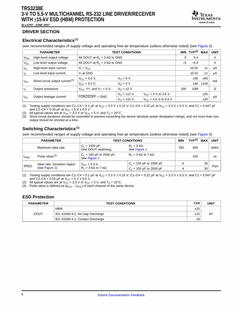
DRIVER SECTION
Switching Characteristics (1)
ESD Protection
TRS3238E3-V TO 5.5-V MULTICHANNEL RS-232 LINE DRIVER/RECEIVERWITH ±15-kV ESD (HBM) PROTECTIONSLLS797–JUNE 2007
xxx
Electrical Characteristics (1)
over recommended ranges of supply voltage and operating free-air temperature (unless otherwise noted) (see Figure 6)
PARAMETER TEST CONDITIONS MIN TYP (2) MAX UNIT
VOH High-level output voltage All DOUT at RL = 3 kΩ to GND 5 5.4 V
VOL Low-level output voltage All DOUT at RL = 3 kΩ to GND –5 –5.4 V
IIH High-level input current VI = VCC ±0.01 ±1 μA
IIL Low-level input current VI at GND ±0.01 ±1 μA
VCC = 3.6 V, VO = 0 V ±35 ±60IOS Short-circuit output current (3) mA
VCC = 5.5 V, VO = 0 V ±40 ±100
ro Output resistance VCC, V+, and V– = 0 V, VO = ±2 V 300 10M Ω
VO = ±12 V, VCC = 3 V to 3.6 V ±25IOZ Output leakage current FORCEOFF = GND μA
VO = ±10 V, VCC = 4.5 V to 5.5 V ±25
(1) Testing supply conditions are C1–C4 = 0.1 μF at VCC = 3.3 V ± 0.15 V; C1–C4 = 0.22 μF at VCC = 3.3 V ± 0.3 V; and C1 = 0.047 μFand C2–C4 = 0.33 μF at VCC = 5 V ± 0.5 V.
(2) All typical values are at VCC = 3.3 V or VCC = 5 V, and TA = 25°C.(3) Short-circuit durations should be controlled to prevent exceeding the device absolute power dissipation ratings, and not more than one
output should be shorted at a time.
over recommended ranges of supply voltage and operating free-air temperature (unless otherwise noted) (see Figure 6)
PARAMETER TEST CONDITIONS MIN TYP (2) MAX UNIT
CL = 1000 pF, RL = 3 kΩ,Maximum data rate 250 400 kbit/sOne DOUT switching, See Figure 1
CL = 150 pF to 2500 pF, RL = 3 kΩ to 7 kΩ,tsk(p) Pulse skew (3) 100 nsSee Figure 2
CL = 150 pF to 1000 pF 6 30Slew rate, transition region VCC = 3.3 V,SR(tr) V/μs(see Figure 1) RL = 3 kΩ to 7 kΩ CL = 150 pF to 2500 pF 4 30
(1) Testing supply conditions are C1–C4 = 0.1 μF at VCC = 3.3 V ± 0.15 V; C1–C4 = 0.22 μF at VCC = 3.3 V ± 0.3 V; and C1 = 0.047 μFand C2–C4 = 0.33 μF at VCC = 5 V ± 0.5 V.
(2) All typical values are at VCC = 3.3 V or VCC = 5 V, and TA = 25°C.(3) Pulse skew is defined as |tPLH – tPHL| of each channel of the same device.
PARAMETER TEST CONDITIONS TYP UNIT
HBM ±15
DOUT IEC 61000-4-2, Air-Gap Discharge ±15 kV
IEC 61000-4-2, Contact Discharge ±8
6 Submit Documentation Feedback
www.ti.com
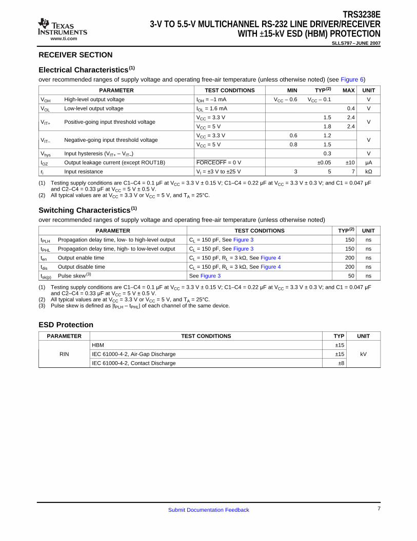
RECEIVER SECTION
Switching Characteristics (1)
ESD Protection
TRS3238E3-V TO 5.5-V MULTICHANNEL RS-232 LINE DRIVER/RECEIVER
WITH ±15-kV ESD (HBM) PROTECTIONSLLS797–JUNE 2007
xxx
Electrical Characteristics (1)
over recommended ranges of supply voltage and operating free-air temperature (unless otherwise noted) (see Figure 6)
PARAMETER TEST CONDITIONS MIN TYP (2) MAX UNIT
VOH High-level output voltage IOH = –1 mA VCC – 0.6 VCC – 0.1 V
VOL Low-level output voltage IOL = 1.6 mA 0.4 V
VCC = 3.3 V 1.5 2.4VIT+ Positive-going input threshold voltage V
VCC = 5 V 1.8 2.4
VCC = 3.3 V 0.6 1.2VIT– Negative-going input threshold voltage V
VCC = 5 V 0.8 1.5
Vhys Input hysteresis (VIT+ – VIT–) 0.3 V
IOZ Output leakage current (except ROUT1B) FORCEOFF = 0 V ±0.05 ±10 μA
ri Input resistance VI = ±3 V to ±25 V 3 5 7 kΩ
(1) Testing supply conditions are C1–C4 = 0.1 μF at VCC = 3.3 V ± 0.15 V; C1–C4 = 0.22 μF at VCC = 3.3 V ± 0.3 V; and C1 = 0.047 μFand C2–C4 = 0.33 μF at VCC = 5 V ± 0.5 V.
(2) All typical values are at VCC = 3.3 V or VCC = 5 V, and TA = 25°C.
over recommended ranges of supply voltage and operating free-air temperature (unless otherwise noted)
PARAMETER TEST CONDITIONS TYP (2) UNIT
tPLH Propagation delay time, low- to high-level output CL = 150 pF, See Figure 3 150 ns
tPHL Propagation delay time, high- to low-level output CL = 150 pF, See Figure 3 150 ns
ten Output enable time CL = 150 pF, RL = 3 kΩ, See Figure 4 200 ns
tdis Output disable time CL = 150 pF, RL = 3 kΩ, See Figure 4 200 ns
tsk(p) Pulse skew (3) See Figure 3 50 ns
(1) Testing supply conditions are C1–C4 = 0.1 μF at VCC = 3.3 V ± 0.15 V; C1–C4 = 0.22 μF at VCC = 3.3 V ± 0.3 V; and C1 = 0.047 μFand C2–C4 = 0.33 μF at VCC = 5 V ± 0.5 V.
(2) All typical values are at VCC = 3.3 V or VCC = 5 V, and TA = 25°C.(3) Pulse skew is defined as |tPLH – tPHL| of each channel of the same device.
PARAMETER TEST CONDITIONS TYP UNIT
HBM ±15
RIN IEC 61000-4-2, Air-Gap Discharge ±15 kV
IEC 61000-4-2, Contact Discharge ±8
7Submit Documentation Feedback
www.ti.com
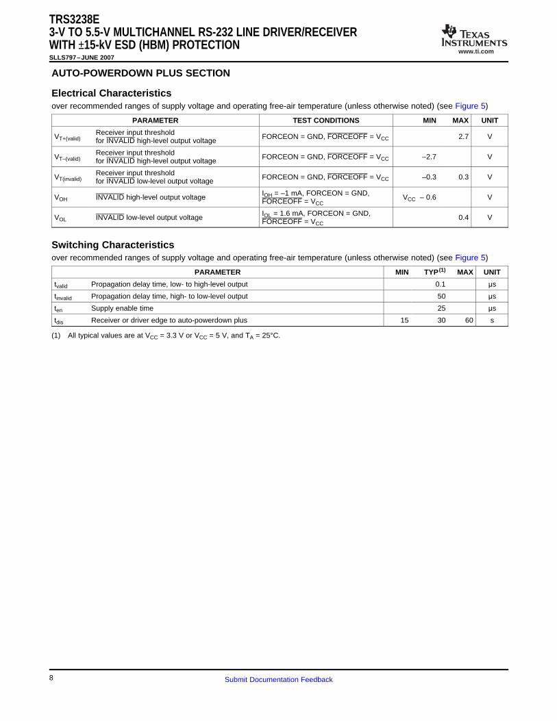
AUTO-POWERDOWN PLUS SECTION
Switching Characteristics
TRS3238E3-V TO 5.5-V MULTICHANNEL RS-232 LINE DRIVER/RECEIVERWITH ±15-kV ESD (HBM) PROTECTIONSLLS797–JUNE 2007
xxx
Electrical Characteristicsover recommended ranges of supply voltage and operating free-air temperature (unless otherwise noted) (see Figure 5)
PARAMETER TEST CONDITIONS MIN MAX UNIT
Receiver input thresholdVT+(valid) FORCEON = GND, FORCEOFF = VCC 2.7 Vfor INVALID high-level output voltage
Receiver input thresholdVT–(valid) FORCEON = GND, FORCEOFF = VCC –2.7 Vfor INVALID high-level output voltage
Receiver input thresholdVT(invalid) FORCEON = GND, FORCEOFF = VCC –0.3 0.3 Vfor INVALID low-level output voltage
IOH = –1 mA, FORCEON = GND,VOH INVALID high-level output voltage VCC – 0.6 VFORCEOFF = VCC
IOL = 1.6 mA, FORCEON = GND,VOL INVALID low-level output voltage 0.4 VFORCEOFF = VCC
over recommended ranges of supply voltage and operating free-air temperature (unless otherwise noted) (see Figure 5)
PARAMETER MIN TYP (1) MAX UNIT
tvalid Propagation delay time, low- to high-level output 0.1 μs
tinvalid Propagation delay time, high- to low-level output 50 μs
ten Supply enable time 25 μs
tdis Receiver or driver edge to auto-powerdown plus 15 30 60 s
(1) All typical values are at VCC = 3.3 V or VCC = 5 V, and TA = 25°C.
8 Submit Documentation Feedback
www.ti.com
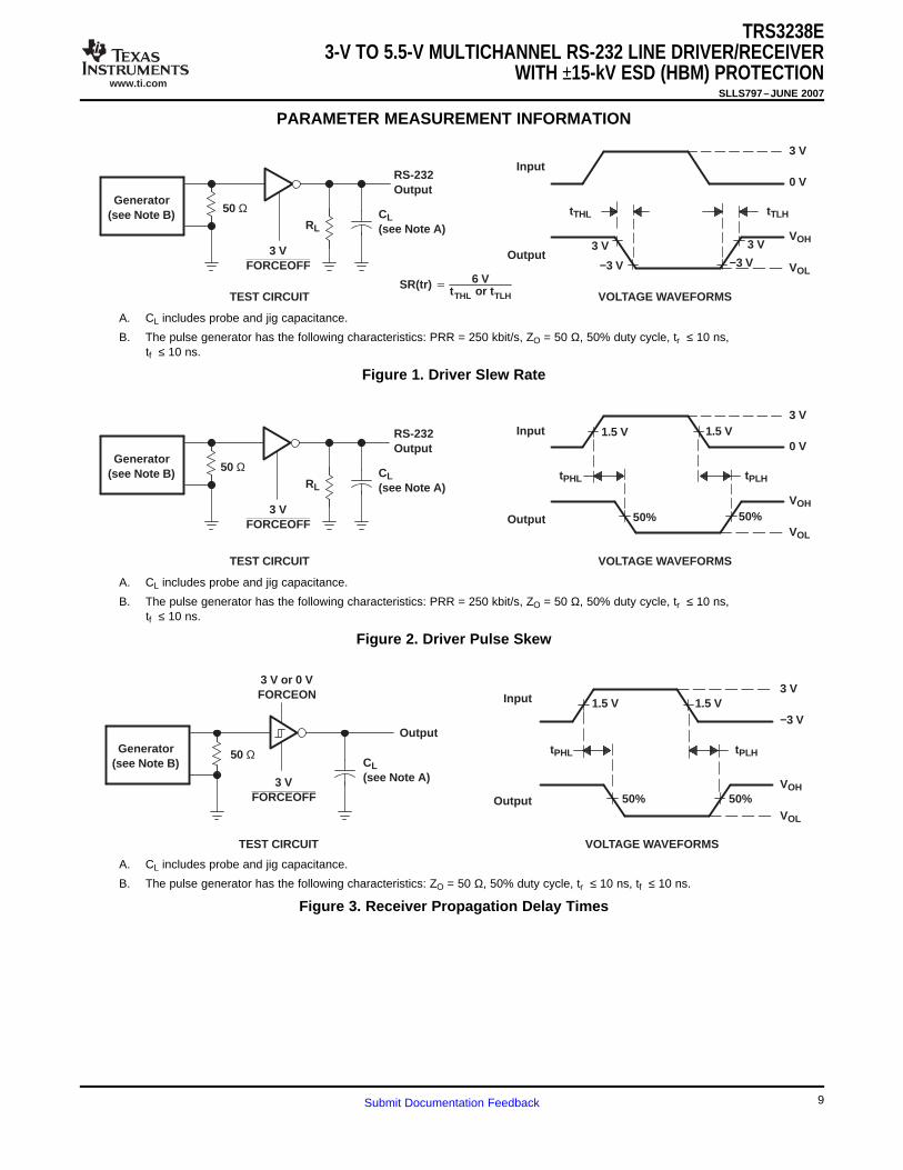
PARAMETER MEASUREMENT INFORMATION
50 Ω
TEST CIRCUIT VOLTAGE WAVEFORMS
−3 V−3 V
3 V3 V
0 V
3 V
Output
Input
VOL
VOH
tTLHGenerator
(see Note B)RL
3 VFORCEOFF
RS-232Output
tTHLCL
(see Note A)
SR(tr) 6 VtTHL or t TLH
50 Ω
TEST CIRCUIT VOLTAGE WAVEFORMS
0 V
3 V
Output
Input
VOL
VOH
tPLH
Generator(see Note B)
RL
3 VFORCEOFF
RS-232Output
tPHLCL
(see Note A)
50% 50%
1.5 V 1.5 V
TEST CIRCUIT VOLTAGE WAVEFORMS
50 Ω
−3 V
3 V
Output
Input
VOL
VOH
tPHLGenerator(see Note B)
tPLH
Output
CL
(see Note A)
3 V or 0 VFORCEON
3 VFORCEOFF
1.5 V 1.5 V
50% 50%
TRS3238E3-V TO 5.5-V MULTICHANNEL RS-232 LINE DRIVER/RECEIVER
WITH ±15-kV ESD (HBM) PROTECTIONSLLS797–JUNE 2007
A. CL includes probe and jig capacitance.
B. The pulse generator has the following characteristics: PRR = 250 kbit/s, ZO = 50 Ω, 50% duty cycle, tr ≤ 10 ns,tf ≤ 10 ns.
Figure 1. Driver Slew Rate
A. CL includes probe and jig capacitance.
B. The pulse generator has the following characteristics: PRR = 250 kbit/s, ZO = 50 Ω, 50% duty cycle, tr ≤ 10 ns,tf ≤ 10 ns.
Figure 2. Driver Pulse Skew
A. CL includes probe and jig capacitance.
B. The pulse generator has the following characteristics: ZO = 50 Ω, 50% duty cycle, tr ≤ 10 ns, tf ≤ 10 ns.
Figure 3. Receiver Propagation Delay Times
9Submit Documentation Feedback
www.ti.com
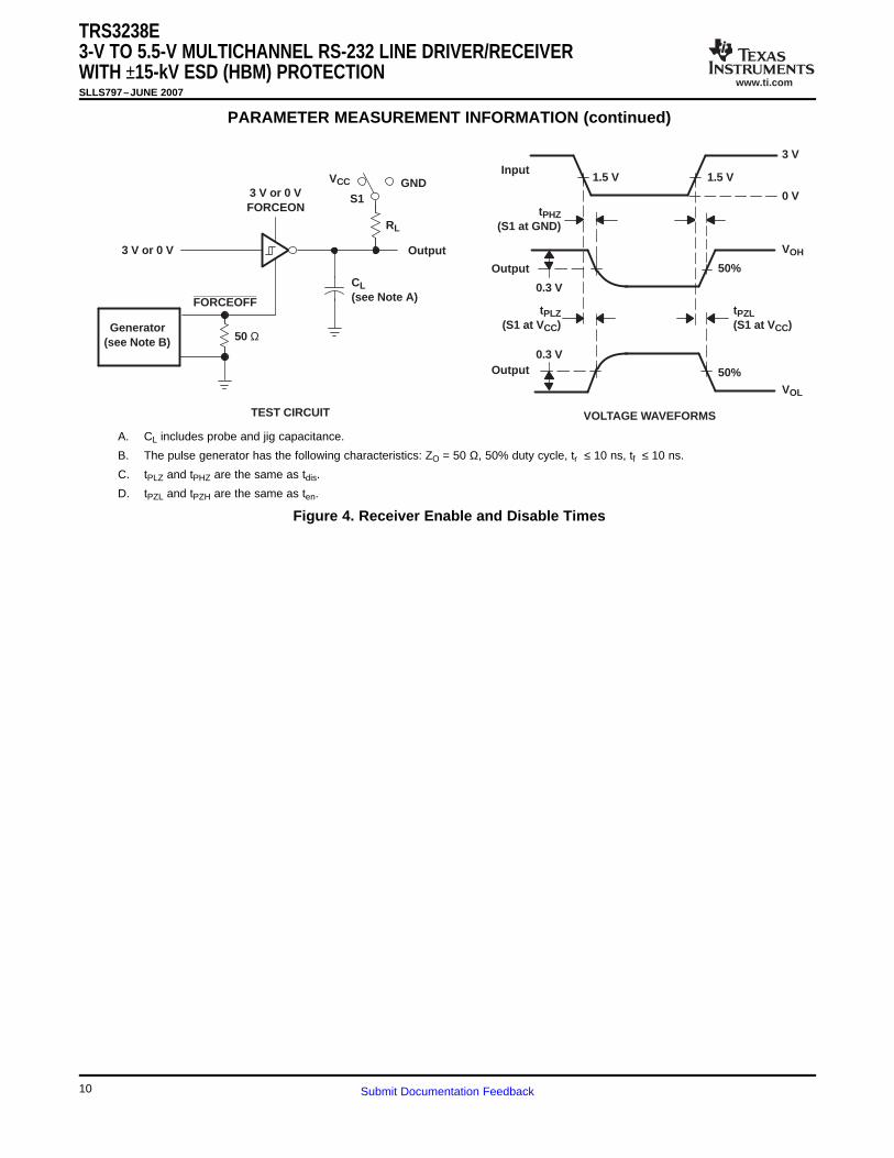
TEST CIRCUIT
50 ΩGenerator
(see Note B)
3 V or 0 V
3 V or 0 VFORCEON
FORCEOFF
RL
S1
VCC GND
CL(see Note A)
Output
VOLTAGE WAVEFORMS
Output
VOL
VOH
3 V
0 V
0.3 V
Output
Input
0.3 V
1.5 V 1.5 V
50%
tPHZ(S1 at GND)
tPLZ(S1 at VCC)
50%
tPZL(S1 at VCC)
TRS3238E3-V TO 5.5-V MULTICHANNEL RS-232 LINE DRIVER/RECEIVERWITH ±15-kV ESD (HBM) PROTECTIONSLLS797–JUNE 2007
PARAMETER MEASUREMENT INFORMATION (continued)
A. CL includes probe and jig capacitance.
B. The pulse generator has the following characteristics: ZO = 50 Ω, 50% duty cycle, tr ≤ 10 ns, tf ≤ 10 ns.
C. tPLZ and tPHZ are the same as tdis.
D. tPZL and tPZH are the same as ten.
Figure 4. Receiver Enable and Disable Times
10 Submit Documentation Feedback
www.ti.com
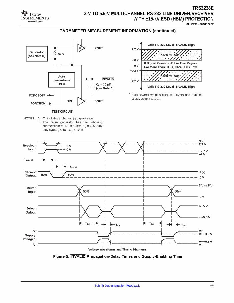
TEST CIRCUIT
50 ΩGenerator
(see Note B)
FORCEOFF
ROUT
FORCEON
Auto-powerdown
Plus
INVALID
DOUTDIN
CL = 30 pF(see Note A)
ÎÎÎÎÎÎÎÎÎÎÎÎÎÎÎÎÎÎÎÎÎÎÎÎÎÎÎÎÎÎÎÎÎÎÎÎÎÎÎÎÎÎÎÎÎÎÎÎÎÎÎÎÎÎÎÎÎÎÎÎÎÎÎÎÎÎÎÎÎÎÎÎÎÎÎÎÎÎÎÎÎÎÎÎÎÎÎÎÎÎÎÎÎÎÎÎÎÎÎ2.7 V
−2.7 V
0.3 V
−0.3 V
0 V
Valid RS-232 Level, INV ALID High
Indeterminate
Indeterminate
If Signal Remains Within This RegionFor More Than 30 µs, INVALID Is Low †
Valid RS-232 Level, INV ALID High
† Auto-powerdown plus disables drivers and reducessupply current to 1 µA.
NOTES: A. CL includes probe and jig capacitance.B. The pulse generator has the following
characteristics: PRR = 5 kbit/s, ZO = 50 Ω, 50%duty cycle, tr ≤ 10 ns, tf ≤ 10 ns.
−2.7 V
ReceiverInput
−3 V
3 V2.7 V
tvalid
VCC
0 V
INVALIDOutput
3 V to 5 V
50%50%
0 V
0 V0 V
50% 50%DriverInput
≈5.5 VDriver
Output
≈ −5.5 V
SupplyVoltages
tdis tentdis ten
V+
V−
V+ −0.3 V
V− +0.3 V
Voltage W aveforms and T iming Diagrams
tinvalid
V+
V−
TRS3238E3-V TO 5.5-V MULTICHANNEL RS-232 LINE DRIVER/RECEIVER
WITH ±15-kV ESD (HBM) PROTECTIONSLLS797–JUNE 2007
PARAMETER MEASUREMENT INFORMATION (continued)
Figure 5. INVALID Propagation-Delay Times and Supply-Enabling Time
11Submit Documentation Feedback
www.ti.com
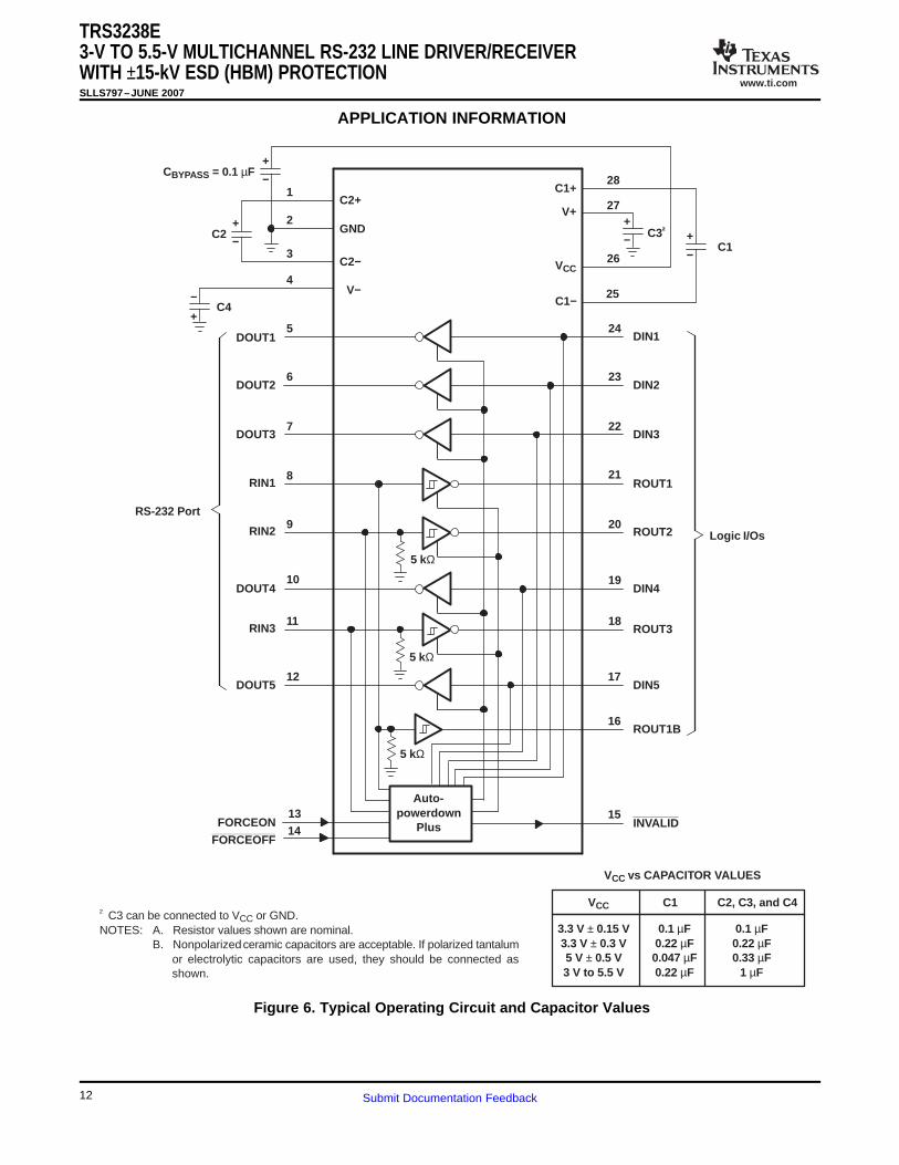
APPLICATION INFORMATION
VCC C1 C2, C3, and C4
3.3 V ± 0.15 V3.3 V ± 0.3 V5 V ± 0.5 V3 V to 5.5 V
0.1 µF0.22 µF0.047 µF0.22 µF
0.1 µF0.22 µF0.33 µF
1 µF
VCC vs CAPACITOR VALUES
Auto-powerdown
Plus
+
−
+
−
+
− +
−
+
−4
5
6
7
8
9
10
11
12
1314
3
1
2
28
27
26
24
25
23
22
21
20
19
18
17
16
15
C2
CBYPASS = 0.1 µF
C1
C4
C2+
GND
C2−
V−
C1+
V+
VCC
C1−
DIN1
DIN2
DIN3
ROUT1
ROUT2
DIN4
ROUT3
DIN5
ROUT1B
INVALID
DOUT1
DOUT2
DOUT3
RIN1
RIN2
DOUT4
RIN3
DOUT5
FORCEON
FORCEOFF
5 kΩ
5 kΩ
5 kΩ
† C3 can be connected to VCC or GND.NOTES: A. Resistor values shown are nominal.
B. Nonpolarized ceramic capacitors are acceptable. If polarized tantalumor electrolytic capacitors are used, they should be connected asshown.
C3†
Logic I/Os
RS-232 Port
TRS3238E3-V TO 5.5-V MULTICHANNEL RS-232 LINE DRIVER/RECEIVERWITH ±15-kV ESD (HBM) PROTECTIONSLLS797–JUNE 2007
Figure 6. Typical Operating Circuit and Capacitor Values
12 Submit Documentation Feedback
PACKAGE OPTION ADDENDUM
www.ti.com 9-Aug-2013
Addendum-Page 1
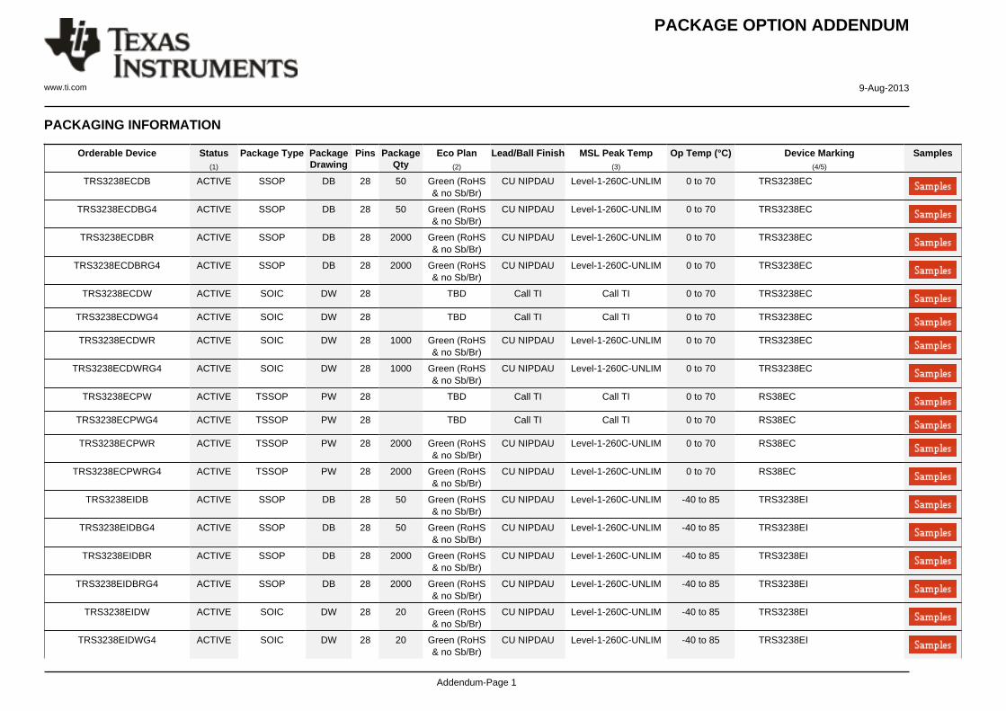
PACKAGING INFORMATION
Orderable Device Status(1)
Package Type PackageDrawing
Pins PackageQty
Eco Plan(2)
Lead/Ball Finish MSL Peak Temp(3)
Op Temp (°C) Device Marking(4/5)
Samples
TRS3238ECDB ACTIVE SSOP DB 28 50 Green (RoHS& no Sb/Br)
CU NIPDAU Level-1-260C-UNLIM 0 to 70 TRS3238EC
TRS3238ECDBG4 ACTIVE SSOP DB 28 50 Green (RoHS& no Sb/Br)
CU NIPDAU Level-1-260C-UNLIM 0 to 70 TRS3238EC
TRS3238ECDBR ACTIVE SSOP DB 28 2000 Green (RoHS& no Sb/Br)
CU NIPDAU Level-1-260C-UNLIM 0 to 70 TRS3238EC
TRS3238ECDBRG4 ACTIVE SSOP DB 28 2000 Green (RoHS& no Sb/Br)
CU NIPDAU Level-1-260C-UNLIM 0 to 70 TRS3238EC
TRS3238ECDW ACTIVE SOIC DW 28 TBD Call TI Call TI 0 to 70 TRS3238EC
TRS3238ECDWG4 ACTIVE SOIC DW 28 TBD Call TI Call TI 0 to 70 TRS3238EC
TRS3238ECDWR ACTIVE SOIC DW 28 1000 Green (RoHS& no Sb/Br)
CU NIPDAU Level-1-260C-UNLIM 0 to 70 TRS3238EC
TRS3238ECDWRG4 ACTIVE SOIC DW 28 1000 Green (RoHS& no Sb/Br)
CU NIPDAU Level-1-260C-UNLIM 0 to 70 TRS3238EC
TRS3238ECPW ACTIVE TSSOP PW 28 TBD Call TI Call TI 0 to 70 RS38EC
TRS3238ECPWG4 ACTIVE TSSOP PW 28 TBD Call TI Call TI 0 to 70 RS38EC
TRS3238ECPWR ACTIVE TSSOP PW 28 2000 Green (RoHS& no Sb/Br)
CU NIPDAU Level-1-260C-UNLIM 0 to 70 RS38EC
TRS3238ECPWRG4 ACTIVE TSSOP PW 28 2000 Green (RoHS& no Sb/Br)
CU NIPDAU Level-1-260C-UNLIM 0 to 70 RS38EC
TRS3238EIDB ACTIVE SSOP DB 28 50 Green (RoHS& no Sb/Br)
CU NIPDAU Level-1-260C-UNLIM -40 to 85 TRS3238EI
TRS3238EIDBG4 ACTIVE SSOP DB 28 50 Green (RoHS& no Sb/Br)
CU NIPDAU Level-1-260C-UNLIM -40 to 85 TRS3238EI
TRS3238EIDBR ACTIVE SSOP DB 28 2000 Green (RoHS& no Sb/Br)
CU NIPDAU Level-1-260C-UNLIM -40 to 85 TRS3238EI
TRS3238EIDBRG4 ACTIVE SSOP DB 28 2000 Green (RoHS& no Sb/Br)
CU NIPDAU Level-1-260C-UNLIM -40 to 85 TRS3238EI
TRS3238EIDW ACTIVE SOIC DW 28 20 Green (RoHS& no Sb/Br)
CU NIPDAU Level-1-260C-UNLIM -40 to 85 TRS3238EI
TRS3238EIDWG4 ACTIVE SOIC DW 28 20 Green (RoHS& no Sb/Br)
CU NIPDAU Level-1-260C-UNLIM -40 to 85 TRS3238EI
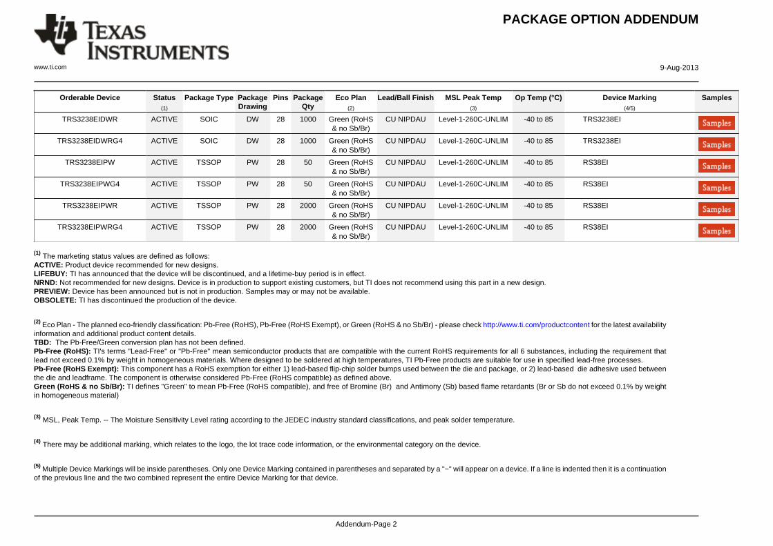
PACKAGE OPTION ADDENDUM
www.ti.com 9-Aug-2013
Addendum-Page 2
Orderable Device Status(1)
Package Type PackageDrawing
Pins PackageQty
Eco Plan(2)
Lead/Ball Finish MSL Peak Temp(3)
Op Temp (°C) Device Marking(4/5)
Samples
TRS3238EIDWR ACTIVE SOIC DW 28 1000 Green (RoHS& no Sb/Br)
CU NIPDAU Level-1-260C-UNLIM -40 to 85 TRS3238EI
TRS3238EIDWRG4 ACTIVE SOIC DW 28 1000 Green (RoHS& no Sb/Br)
CU NIPDAU Level-1-260C-UNLIM -40 to 85 TRS3238EI
TRS3238EIPW ACTIVE TSSOP PW 28 50 Green (RoHS& no Sb/Br)
CU NIPDAU Level-1-260C-UNLIM -40 to 85 RS38EI
TRS3238EIPWG4 ACTIVE TSSOP PW 28 50 Green (RoHS& no Sb/Br)
CU NIPDAU Level-1-260C-UNLIM -40 to 85 RS38EI
TRS3238EIPWR ACTIVE TSSOP PW 28 2000 Green (RoHS& no Sb/Br)
CU NIPDAU Level-1-260C-UNLIM -40 to 85 RS38EI
TRS3238EIPWRG4 ACTIVE TSSOP PW 28 2000 Green (RoHS& no Sb/Br)
CU NIPDAU Level-1-260C-UNLIM -40 to 85 RS38EI
(1) The marketing status values are defined as follows:ACTIVE: Product device recommended for new designs.LIFEBUY: TI has announced that the device will be discontinued, and a lifetime-buy period is in effect.NRND: Not recommended for new designs. Device is in production to support existing customers, but TI does not recommend using this part in a new design.PREVIEW: Device has been announced but is not in production. Samples may or may not be available.OBSOLETE: TI has discontinued the production of the device.
(2) Eco Plan - The planned eco-friendly classification: Pb-Free (RoHS), Pb-Free (RoHS Exempt), or Green (RoHS & no Sb/Br) - please check http://www.ti.com/productcontent for the latest availabilityinformation and additional product content details.TBD: The Pb-Free/Green conversion plan has not been defined.Pb-Free (RoHS): TI's terms "Lead-Free" or "Pb-Free" mean semiconductor products that are compatible with the current RoHS requirements for all 6 substances, including the requirement thatlead not exceed 0.1% by weight in homogeneous materials. Where designed to be soldered at high temperatures, TI Pb-Free products are suitable for use in specified lead-free processes.Pb-Free (RoHS Exempt): This component has a RoHS exemption for either 1) lead-based flip-chip solder bumps used between the die and package, or 2) lead-based die adhesive used betweenthe die and leadframe. The component is otherwise considered Pb-Free (RoHS compatible) as defined above.Green (RoHS & no Sb/Br): TI defines "Green" to mean Pb-Free (RoHS compatible), and free of Bromine (Br) and Antimony (Sb) based flame retardants (Br or Sb do not exceed 0.1% by weightin homogeneous material)
(3) MSL, Peak Temp. -- The Moisture Sensitivity Level rating according to the JEDEC industry standard classifications, and peak solder temperature.
(4) There may be additional marking, which relates to the logo, the lot trace code information, or the environmental category on the device.
(5) Multiple Device Markings will be inside parentheses. Only one Device Marking contained in parentheses and separated by a "~" will appear on a device. If a line is indented then it is a continuationof the previous line and the two combined represent the entire Device Marking for that device.
PACKAGE OPTION ADDENDUM
www.ti.com 9-Aug-2013
Addendum-Page 3
Important Information and Disclaimer:The information provided on this page represents TI's knowledge and belief as of the date that it is provided. TI bases its knowledge and belief on informationprovided by third parties, and makes no representation or warranty as to the accuracy of such information. Efforts are underway to better integrate information from third parties. TI has taken andcontinues to take reasonable steps to provide representative and accurate information but may not have conducted destructive testing or chemical analysis on incoming materials and chemicals.TI and TI suppliers consider certain information to be proprietary, and thus CAS numbers and other limited information may not be available for release.
In no event shall TI's liability arising out of such information exceed the total purchase price of the TI part(s) at issue in this document sold by TI to Customer on an annual basis.
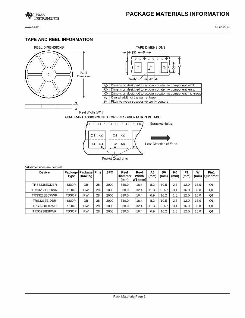
TAPE AND REEL INFORMATION
*All dimensions are nominal
Device PackageType
PackageDrawing
Pins SPQ ReelDiameter
(mm)
ReelWidth
W1 (mm)
A0(mm)
B0(mm)
K0(mm)
P1(mm)
W(mm)
Pin1Quadrant
TRS3238ECDBR SSOP DB 28 2000 330.0 16.4 8.2 10.5 2.5 12.0 16.0 Q1
TRS3238ECDWR SOIC DW 28 1000 330.0 32.4 11.35 18.67 3.1 16.0 32.0 Q1
TRS3238ECPWR TSSOP PW 28 2000 330.0 16.4 6.9 10.2 1.8 12.0 16.0 Q1
TRS3238EIDBR SSOP DB 28 2000 330.0 16.4 8.2 10.5 2.5 12.0 16.0 Q1
TRS3238EIDWR SOIC DW 28 1000 330.0 32.4 11.35 18.67 3.1 16.0 32.0 Q1
TRS3238EIPWR TSSOP PW 28 2000 330.0 16.4 6.9 10.2 1.8 12.0 16.0 Q1
PACKAGE MATERIALS INFORMATION
www.ti.com 5-Feb-2013
Pack Materials-Page 1

*All dimensions are nominal
Device Package Type Package Drawing Pins SPQ Length (mm) Width (mm) Height (mm)
TRS3238ECDBR SSOP DB 28 2000 367.0 367.0 38.0
TRS3238ECDWR SOIC DW 28 1000 367.0 367.0 55.0
TRS3238ECPWR TSSOP PW 28 2000 367.0 367.0 38.0
TRS3238EIDBR SSOP DB 28 2000 367.0 367.0 38.0
TRS3238EIDWR SOIC DW 28 1000 367.0 367.0 55.0
TRS3238EIPWR TSSOP PW 28 2000 367.0 367.0 38.0
PACKAGE MATERIALS INFORMATION
www.ti.com 5-Feb-2013
Pack Materials-Page 2

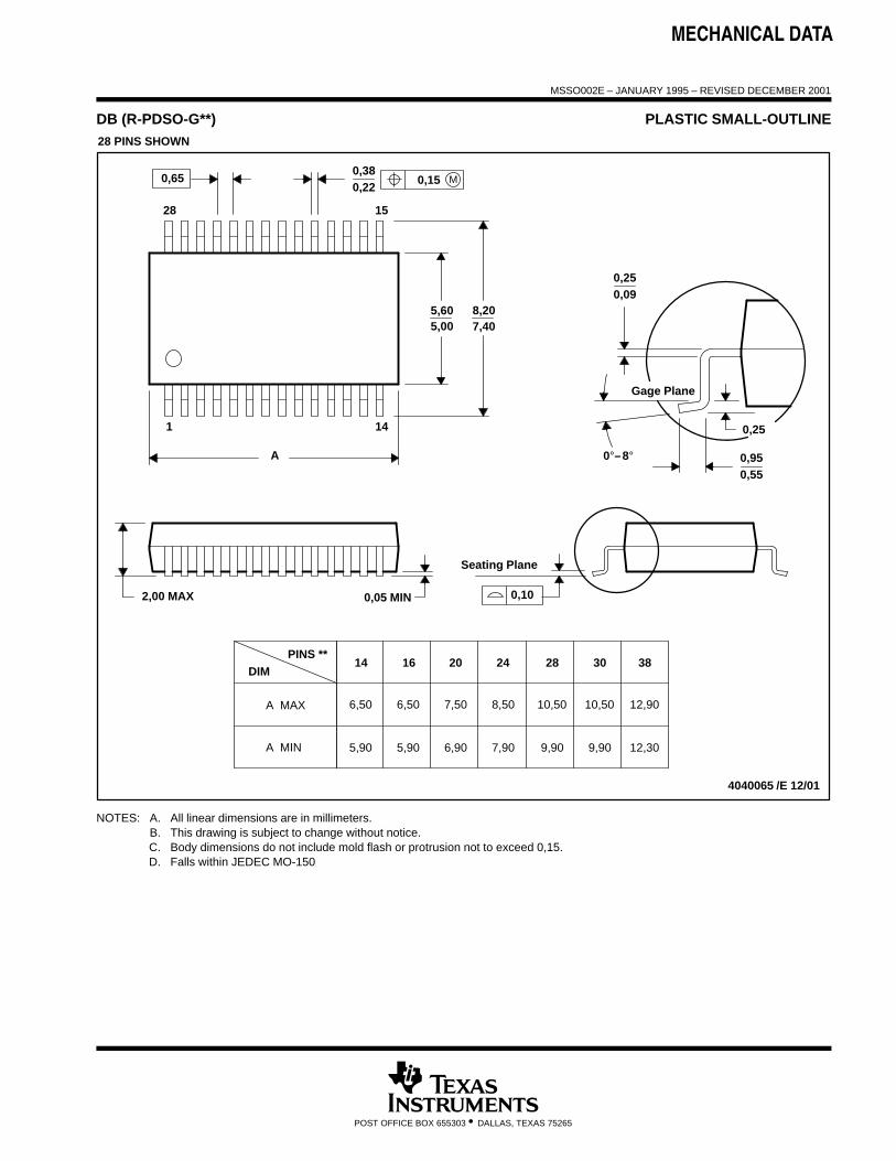
MECHANICAL DATA
MSSO002E – JANUARY 1995 – REVISED DECEMBER 2001
POST OFFICE BOX 655303 • DALLAS, TEXAS 75265
DB (R-PDSO-G**) PLASTIC SMALL-OUTLINE
4040065 /E 12/01
28 PINS SHOWN
Gage Plane
8,207,40
0,550,95
0,25
38
12,90
12,30
28
10,50
24
8,50
Seating Plane
9,907,90
30
10,50
9,90
0,38
5,605,00
15
0,22
14
A
28
1
2016
6,506,50
14
0,05 MIN
5,905,90
DIM
A MAX
A MIN
PINS **
2,00 MAX
6,90
7,50
0,65 M0,15
0°–8°
0,10
0,090,25
NOTES: A. All linear dimensions are in millimeters.B. This drawing is subject to change without notice.C. Body dimensions do not include mold flash or protrusion not to exceed 0,15.D. Falls within JEDEC MO-150
IMPORTANT NOTICE
Texas Instruments Incorporated and its subsidiaries (TI) reserve the right to make corrections, enhancements, improvements and otherchanges to its semiconductor products and services per JESD46, latest issue, and to discontinue any product or service per JESD48, latestissue. Buyers should obtain the latest relevant information before placing orders and should verify that such information is current andcomplete. All semiconductor products (also referred to herein as “components”) are sold subject to TI’s terms and conditions of salesupplied at the time of order acknowledgment.
TI warrants performance of its components to the specifications applicable at the time of sale, in accordance with the warranty in TI’s termsand conditions of sale of semiconductor products. Testing and other quality control techniques are used to the extent TI deems necessaryto support this warranty. Except where mandated by applicable law, testing of all parameters of each component is not necessarilyperformed.
TI assumes no liability for applications assistance or the design of Buyers’ products. Buyers are responsible for their products andapplications using TI components. To minimize the risks associated with Buyers’ products and applications, Buyers should provideadequate design and operating safeguards.
TI does not warrant or represent that any license, either express or implied, is granted under any patent right, copyright, mask work right, orother intellectual property right relating to any combination, machine, or process in which TI components or services are used. Informationpublished by TI regarding third-party products or services does not constitute a license to use such products or services or a warranty orendorsement thereof. Use of such information may require a license from a third party under the patents or other intellectual property of thethird party, or a license from TI under the patents or other intellectual property of TI.
Reproduction of significant portions of TI information in TI data books or data sheets is permissible only if reproduction is without alterationand is accompanied by all associated warranties, conditions, limitations, and notices. TI is not responsible or liable for such altereddocumentation. Information of third parties may be subject to additional restrictions.
Resale of TI components or services with statements different from or beyond the parameters stated by TI for that component or servicevoids all express and any implied warranties for the associated TI component or service and is an unfair and deceptive business practice.TI is not responsible or liable for any such statements.
Buyer acknowledges and agrees that it is solely responsible for compliance with all legal, regulatory and safety-related requirementsconcerning its products, and any use of TI components in its applications, notwithstanding any applications-related information or supportthat may be provided by TI. Buyer represents and agrees that it has all the necessary expertise to create and implement safeguards whichanticipate dangerous consequences of failures, monitor failures and their consequences, lessen the likelihood of failures that might causeharm and take appropriate remedial actions. Buyer will fully indemnify TI and its representatives against any damages arising out of the useof any TI components in safety-critical applications.
In some cases, TI components may be promoted specifically to facilitate safety-related applications. With such components, TI’s goal is tohelp enable customers to design and create their own end-product solutions that meet applicable functional safety standards andrequirements. Nonetheless, such components are subject to these terms.
No TI components are authorized for use in FDA Class III (or similar life-critical medical equipment) unless authorized officers of the partieshave executed a special agreement specifically governing such use.
Only those TI components which TI has specifically designated as military grade or “enhanced plastic” are designed and intended for use inmilitary/aerospace applications or environments. Buyer acknowledges and agrees that any military or aerospace use of TI componentswhich have not been so designated is solely at the Buyer's risk, and that Buyer is solely responsible for compliance with all legal andregulatory requirements in connection with such use.
TI has specifically designated certain components as meeting ISO/TS16949 requirements, mainly for automotive use. In any case of use ofnon-designated products, TI will not be responsible for any failure to meet ISO/TS16949.
Products Applications
Audio www.ti.com/audio Automotive and Transportation www.ti.com/automotive
Amplifiers amplifier.ti.com Communications and Telecom www.ti.com/communications
Data Converters dataconverter.ti.com Computers and Peripherals www.ti.com/computers
DLP® Products www.dlp.com Consumer Electronics www.ti.com/consumer-apps
DSP dsp.ti.com Energy and Lighting www.ti.com/energy
Clocks and Timers www.ti.com/clocks Industrial www.ti.com/industrial
Interface interface.ti.com Medical www.ti.com/medical
Logic logic.ti.com Security www.ti.com/security
Power Mgmt power.ti.com Space, Avionics and Defense www.ti.com/space-avionics-defense
Microcontrollers microcontroller.ti.com Video and Imaging www.ti.com/video
RFID www.ti-rfid.com
OMAP Applications Processors www.ti.com/omap TI E2E Community e2e.ti.com
Wireless Connectivity www.ti.com/wirelessconnectivity
Mailing Address: Texas Instruments, Post Office Box 655303, Dallas, Texas 75265Copyright © 2013, Texas Instruments Incorporated