transistor models - quantum materials at ubc
TRANSCRIPT

ampel
Transistor Models
• Review of Transistor Fundamentals
• Simple Current Amplifier Model
• Transistor Switch Example• Common Emitter Amplifier Example
• Transistor as a Transductance Device - Ebers-Moll Model
• Other Models: h-parameter, Gummel-Poon charge control model.
ampel
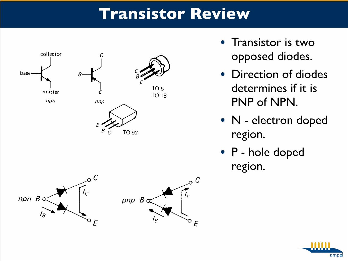
Transistor Review
• Transistor is two opposed diodes.
• Direction of diodes determines if it is PNP of NPN.
• N - electron doped region.
• P - hole doped region.
ampel
Transistor Review
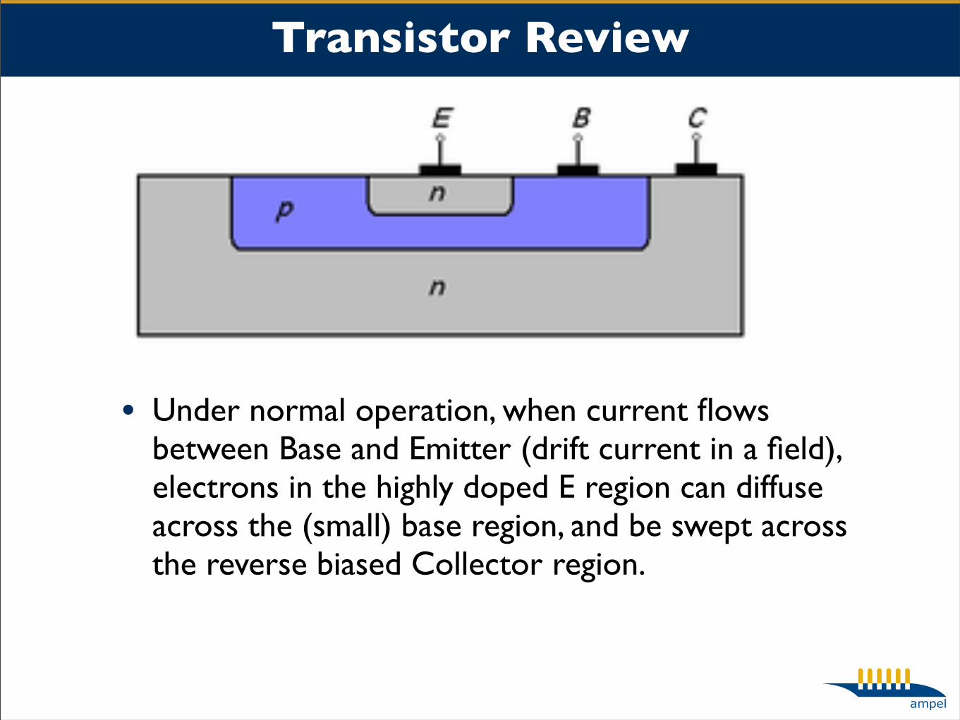
• Under normal operation, when current flows between Base and Emitter (drift current in a field), electrons in the highly doped E region can diffuse across the (small) base region, and be swept across the reverse biased Collector region.
ampel
Current Amplifier Model
1. Collector must be more positive than emitter.
2. The Base-Emitter and Base-Collector junctions behave like diodes. Normally, the BE is forward biased, and the BC is reverse biased.
3. Transistors have maximum values of Ic, Ib and Vce that cannot be exceeded. Exceeding these values results in a broken transistor.
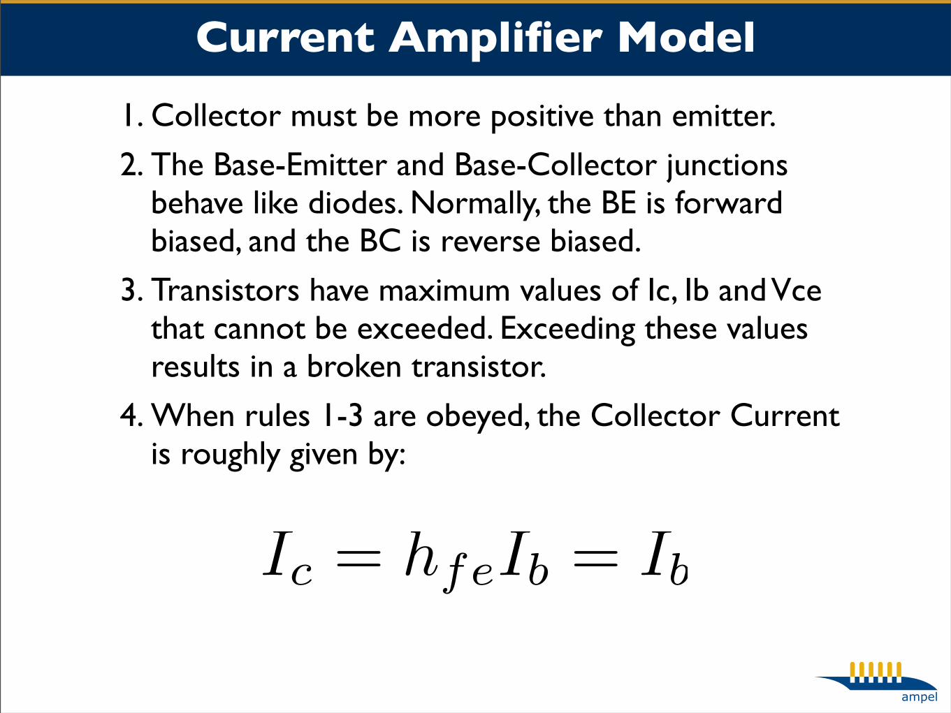
4. When rules 1-3 are obeyed, the Collector Current is roughly given by:
Ic = hfeIb = Ib
ampel
Current Amplifier Model
• hfe is typically 100, but varies wildly with temperature, Ic, and between transistors.
• Ic is not due to diode conduction, it is due to diffusion of carriers from the heavily doped emitter region (which only occurs when the Base-Emitter region if forward biased).
• Some simple examples:
• simple switch• Common-Emitter Amplifier
ampel
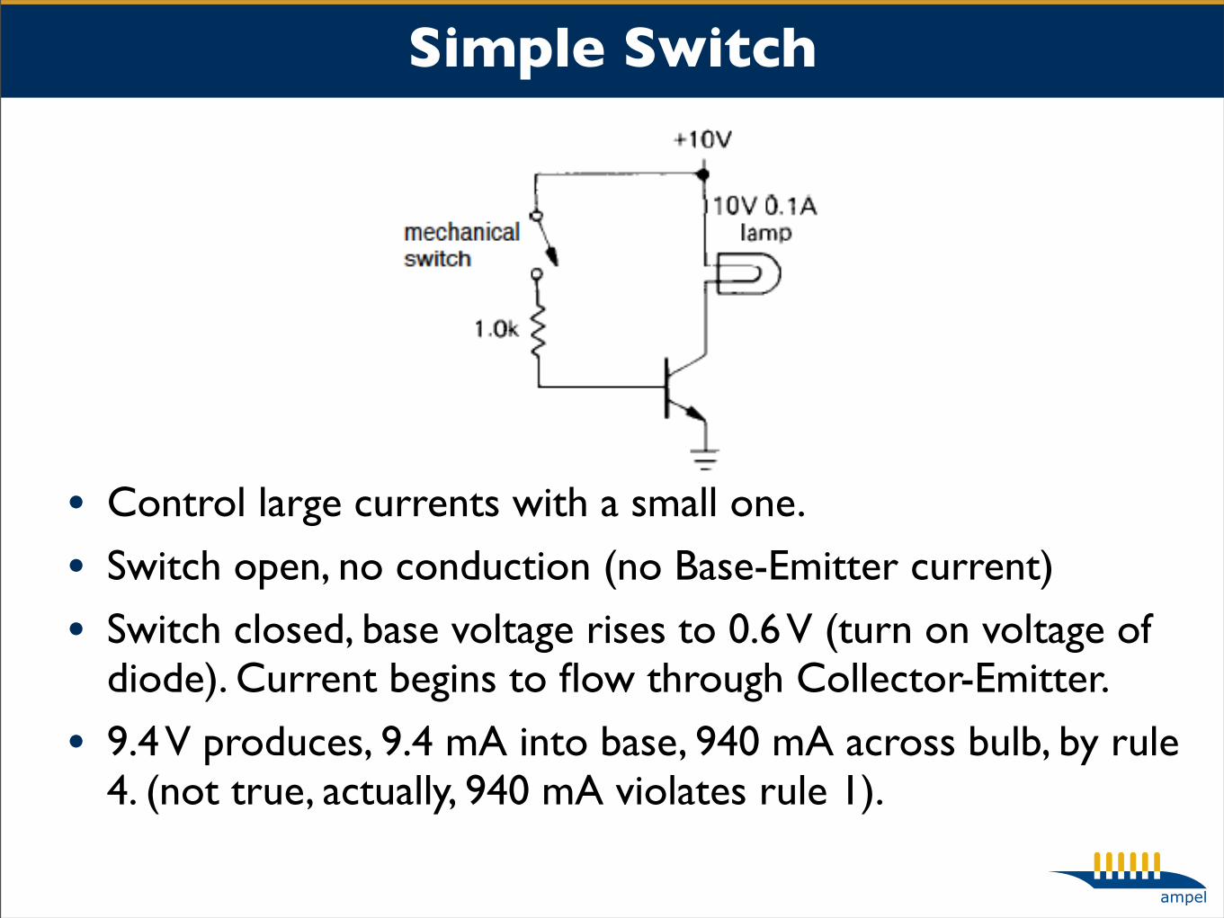
Simple Switch
• Control large currents with a small one.
• Switch open, no conduction (no Base-Emitter current)
• Switch closed, base voltage rises to 0.6 V (turn on voltage of diode). Current begins to flow through Collector-Emitter.
• 9.4 V produces, 9.4 mA into base, 940 mA across bulb, by rule 4. (not true, actually, 940 mA violates rule 1).
ampel
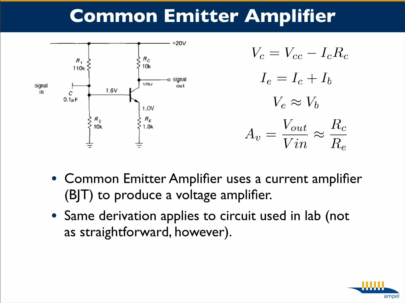
Common Emitter Amplifier
• Common Emitter Amplifier uses a current amplifier (BJT) to produce a voltage amplifier.
• Same derivation applies to circuit used in lab (not as straightforward, however).
Vc = Vcc − IcRc
Ie = Ic + Ib
Ve ≈ Vb
Av =Vout
V in≈ Rc
Re
ampel
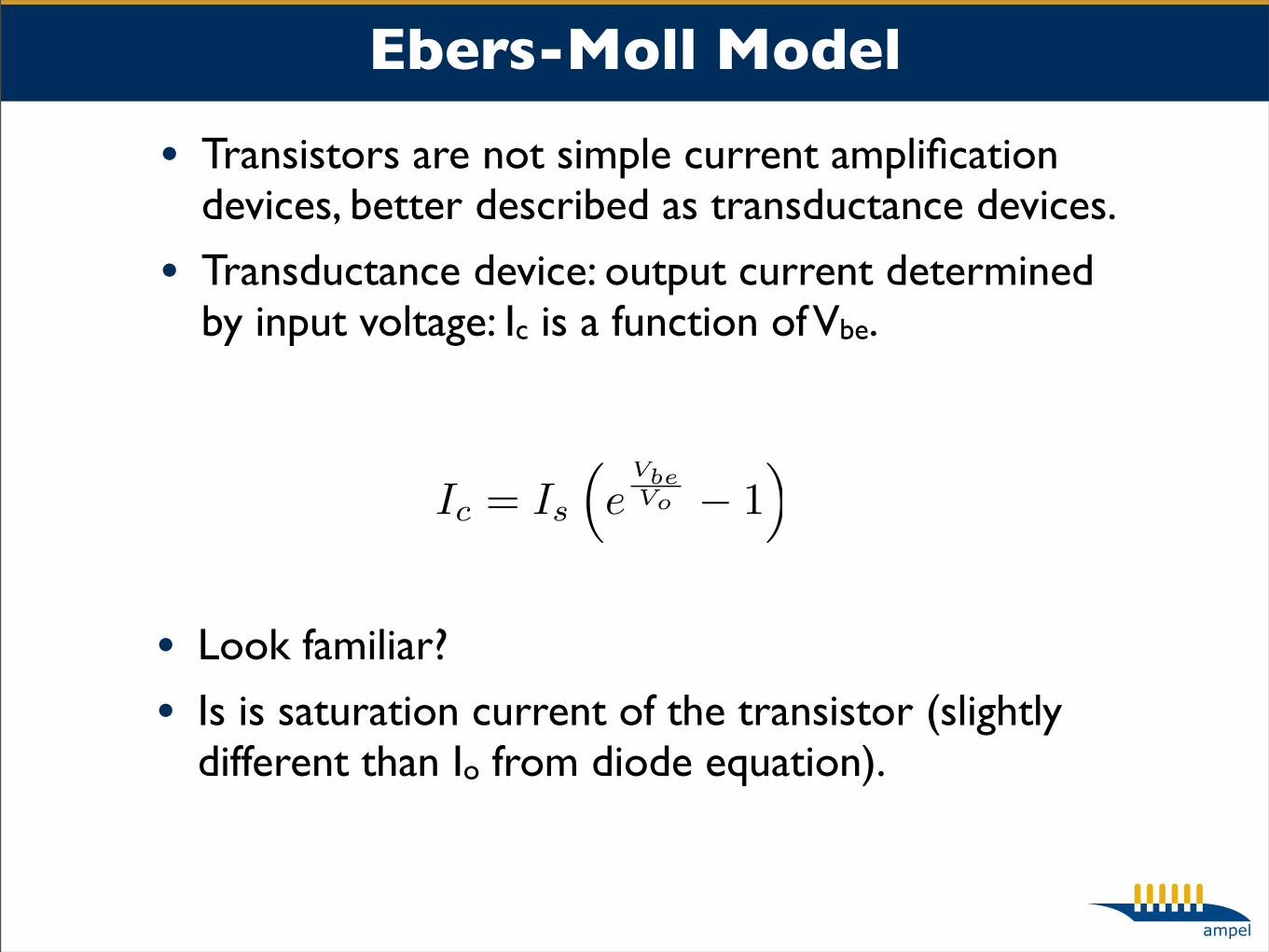
Ebers-Moll Model
• Transistors are not simple current amplification devices, better described as transductance devices.
• Transductance device: output current determined by input voltage: Ic is a function of Vbe.
Ic = Is
(e
VbeVo − 1
)
• Look familiar?
• Is is saturation current of the transistor (slightly different than Io from diode equation).
ampel
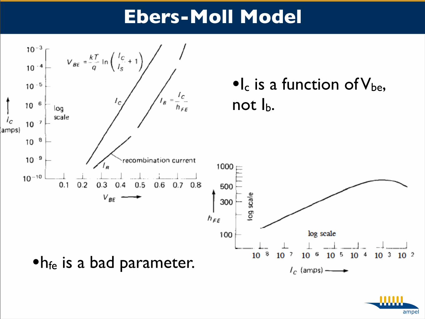
Ebers-Moll Model
•Ic is a function of Vbe,not Ib.
•hfe is a bad parameter.
ampel
Other Models
• Many, many models of transistor action.
• h-parameter and hybrid-pi model are similar, designed for small signals, involve using a equivelant circuit to model transistor behaviour. Makes it easy to describe frequency dependance.
• Gunner-Poon Model, similar to EM model, but more complicated/more correct.
• Wikipedia is a good place to start.
• Datasheets are gold. (google “2n3904 datasheet”)
5.6. BJT circuit models 5.6.1. Small signal model (hybrid pi model) 5.6.2. Large signal model (Charge control model) 5.6.3. SPICE model
Title Page Table of Contents Help Copyright © B. Van Zeghbroeck, 2004
Chapter 5: Bipolar Junction Transistors
A large variety of bipolar junction transistor models have been developed. One distinguishes between small signal and large signal models. We will discuss here first the hybrid pi model, a small signal model, which lenitself well to small signal design and analysis. The next model is the charge control model, which is particularwell suited to analyze the large-signal transient behavior of a bipolar transistor. And we conclude with the derivation of the SPICE model parameters.
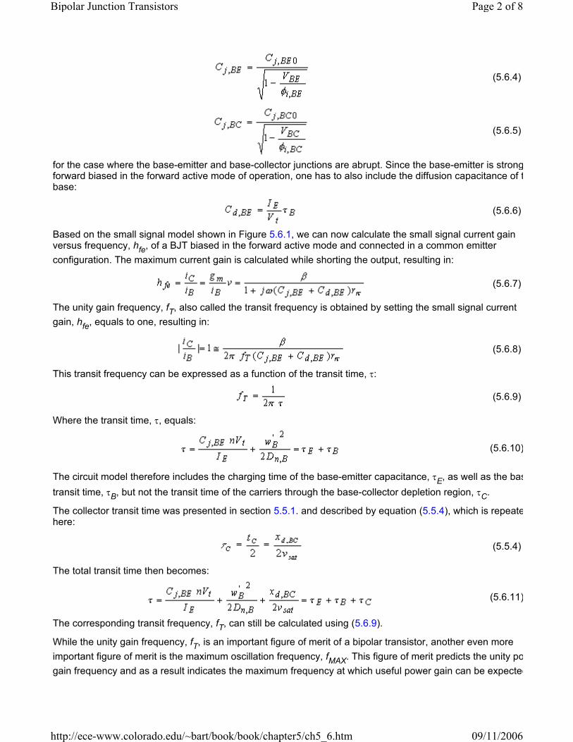
5.6.1. Small signal model (hybrid pi model)
The hybrid pi model of a BJT is a small signal model, named after the “π”-like equivalent circuit for a bipolar junction transistor. The model is shown in Figure 5.6.1. It consists of an input impedance, rπ, an output impedance r0, and a voltage controlled current source described by the transconductance, gm. In addition it contains the base-emitter capacitances, the junction capacitance, Cj,BE, and the diffusion capacitance, Cd,BEand the base-collector junction capacitance, Cj,BC, also referred to as the Miller capacitance.
Figure 5.6.1. : Small signal model (hybrid pi model) of a bipolar junction transistor.The transconductance, gm, of a bipolar transistor is defined as the change in the collector current divided by change of the base-emitter voltage. Using (5.4.6) one obtains:
(5.6.1)
The base input resistance, rπ, is defined as the change of the emitter-base voltage divided by the change of tbase current.
(5.6.2)
The output resistance, ro, is defined as:
(5.6.3)
The base-emitter and base-collector junction capacitances are given by:
Page 1 of 8Bipolar Junction Transistors
09/11/2006http://ece-www.colorado.edu/~bart/book/book/chapter5/ch5_6.htm
(5.6.4)
(5.6.5)
for the case where the base-emitter and base-collector junctions are abrupt. Since the base-emitter is strongforward biased in the forward active mode of operation, one has to also include the diffusion capacitance of tbase:
(5.6.6)
Based on the small signal model shown in Figure 5.6.1, we can now calculate the small signal current gain versus frequency, hfe, of a BJT biased in the forward active mode and connected in a common emitter configuration. The maximum current gain is calculated while shorting the output, resulting in:
(5.6.7)
The unity gain frequency, fT, also called the transit frequency is obtained by setting the small signal current gain, hfe, equals to one, resulting in:
(5.6.8)
This transit frequency can be expressed as a function of the transit time, τ:
(5.6.9)
Where the transit time, τ, equals:
(5.6.10)
The circuit model therefore includes the charging time of the base-emitter capacitance, τE, as well as the bastransit time, τB, but not the transit time of the carriers through the base-collector depletion region, τC.
The collector transit time was presented in section 5.5.1. and described by equation (5.5.4), which is repeatehere:
(5.5.4)
The total transit time then becomes:
(5.6.11)
The corresponding transit frequency, fT, can still be calculated using (5.6.9).
While the unity gain frequency, fT, is an important figure of merit of a bipolar transistor, another even more important figure of merit is the maximum oscillation frequency, fMAX. This figure of merit predicts the unity pogain frequency and as a result indicates the maximum frequency at which useful power gain can be expected
Page 2 of 8Bipolar Junction Transistors
09/11/2006http://ece-www.colorado.edu/~bart/book/book/chapter5/ch5_6.htm
from a device. The maximum oscillation frequency, fMAX, is linked to the transit frequency, fT, and is obtainedfrom:
(5.6.12)
Where RB is the total base resistance and Cj,BC is the base-collector capacitance. The total base resistance consists of the series connection of metal-semiconductor contact resistance, the resistance between the bascontact metal and the emitter and the intrinsic base resistance. Assuming a base contact, which is longer thathe penetration depth this base resistance equals
(5.6.13)
for a one-sided base contact, where Rs,c, Rs,BE and Rs are the sheet resistances under the base contact, between the base contact and the emitter and underneath the emitter respectively. Ls,E is the emitter stripe length of the emitter, Ws,E is the emitter stripe width of the emitter and ∆L is the alignment distance between base contact and emitter. For a double-sided base contact, the total base resistance equals
(5.6.14)
The base-collector capacitance equals:
(5.6.15)
Where AC is the base-collector area.
5.6.2. Large signal model (Charge control model)
The charge control model of a bipolar transistor is an extension of the charge control model of a p-n diode. Assuming the “short” diode model to be valid, one can express the device currents as a function of the chargin each region, divided by the corresponding transit or lifetime. In the general case one considers the forwardbias charges as well as the reverse bias charges. This results in:
(5.6.16)
(5.6.17)
(5.6.18)
Under forward active mode of operation, this model can be simplified since the reverse mode components cabe ignored. A transient model can be obtained by adding the rate of change of the charges over time. To furtsimplify the model, we also ignore the minority carrier charge, ∆Qp,E, in the emitter. This results in the followiequations:
(5.6.19)
(5.6.20)
Page 3 of 8Bipolar Junction Transistors
09/11/2006http://ece-www.colorado.edu/~bart/book/book/chapter5/ch5_6.htm
(5.6.21)
As an example we now apply this charge control model to the abrupt switching of a bipolar transistor. Considthe circuit shown in Figure 5.3.2.(a). As one applies a positive voltage to the base, the base-emitter junction wbecome forward biased so that the collector current will start to rise. The input is then connected to a negativsupply voltage, VR. This reverses the base current and the base-emitter junction capacitance is discharged. After this transient, the transistor is eventually turned off and the collector current reduces back to zero. A fulanalysis would require solving the charge control model equations simultaneously, while adding the external circuit equations. Such approach requires numeric simulation tools. To simplify this analysis and provide insight, we now assume that the base current is constant before and aftswitching. This approximation is very good under forward bias since the base-emitter voltage is almost constUnder reverse bias, the base current will vary as the base-emitter voltage varies, but conceivably one could design a circuit that does provide a constant reverse current. The turn-on of the BJT consists of an initial delay time, td,1, during which the base-emitter junction capacitancis charged. This delay is followed by the increase of the collector current, quantified by the rise time, trise. Thrise time is obtained by applying the charge control equation for the base current, while applying a base curreIBB with the voltage source VBB:
(5.6.22)
where:
(5.6.23)
This differential equation can be solved resulting in:
(5.6.24)
If the device does not reach saturation, the charge reaches its steady state value with a time constant tr,B, whequals the base transit time of the BJT. The corresponding collector current will be proportional to the excessminority carrier charge until the device reaches saturation or:
(5.6.25)
A larger base voltage, VBB, will therefore result in a larger charging current, IBB, which in turn decreases the time and causes the BJT to saturate more quickly. There also will be more excess minority carrier charge stoin the base region after the BJT is turned on. The rise time, trise, is then obtained by finding the time when thsaturation current is reached or:
(5.6.26)
While switching back to the negative power supply, VR, the base current is reversed. As long as significant charge is still stored in the base region, the collector current will continue to exist. Only after this excess char
Page 4 of 8Bipolar Junction Transistors
09/11/2006http://ece-www.colorado.edu/~bart/book/book/chapter5/ch5_6.htm
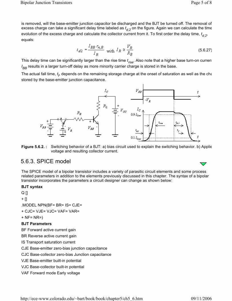
is removed, will the base-emitter junction capacitor be discharged and the BJT be turned off. The removal of excess charge can take a significant delay time labeled as td,2 on the figure. Again we can calculate the timeevolution of the excess charge and calculate the collector current from it. To first order the delay time, td,2, equals:
(5.6.27)
This delay time can be significantly larger than the rise time trise. Also note that a higher base turn-on currentIBB results in a larger turn-off delay as more minority carrier charge is stored in the base.
The actual fall time, tf, depends on the remaining storage charge at the onset of saturation as well as the chastored by the base-emitter junction capacitance.
Figure 5.6.2. : Switching behavior of a BJT: a) bias circuit used to explain the switching behavior. b) Applievoltage and resulting collector current.
5.6.3. SPICE model
The SPICE model of a bipolar transistor includes a variety of parasitic circuit elements and some process related parameters in addition to the elements previously discussed in this chapter. The syntax of a bipolar transistor incorporates the parameters a circuit designer can change as shown below: BJT syntax Q [] + [] .MODEL NPN(BF= BR= IS= CJE= + CJC= VJE= VJC= VAF= VAR= + NF= NR=) BJT Parameters BF Forward active current gain BR Reverse active current gain IS Transport saturation current CJE Base-emitter zero-bias junction capacitance CJC Base-collector zero-bias Junction capacitance VJE Base-emitter built-in potential VJC Base-collector built-in potential VAF Forward mode Early voltage
Page 5 of 8Bipolar Junction Transistors
09/11/2006http://ece-www.colorado.edu/~bart/book/book/chapter5/ch5_6.htm
VAR Reverse mode Early voltage NF Forward mode ideality factor NR Reverse mode ideality factor Example: Q1 3 2 1 BJTNAME .MODEL BJTNAME NPN(BF=100 CJC=20pf CJE=20pf IS=1E-16) where Q1 is one specific transistor in the circuit, while the transistor model "BJTNAME" uses the built-in modNPN to specify the process and technology related parameters of the BJT. The built-in model PNP is used fon-p bipolar transistors. A list of SPICE parameters and their relation to the parameters discussed in this text iprovided in the table below.
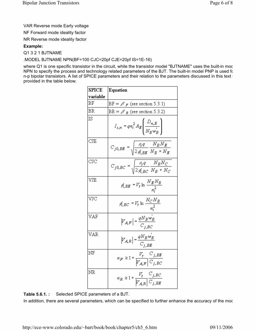
Table 5.6.1. : Selected SPICE parameters of a BJT.In addition, there are several parameters, which can be specified to further enhance the accuracy of the mod
Page 6 of 8Bipolar Junction Transistors
09/11/2006http://ece-www.colorado.edu/~bart/book/book/chapter5/ch5_6.htm

such as: RB base resistance RE emitter resistance RC collector resistance MJE base-emitter capacitance exponent MJC base-collector capacitance exponent EG energy gap for temperature effect on IS The exponents NJE and MJC are used to calculate the voltage dependence of the base-emitter and base-collector junction capacitances using:
(5.6.28)
(5.6.29)
This exponent allows the choice between a uniformly doped junction (m = ½), a linearly graded junction (m =1/3) or an arbitrarily graded junction for which the exponent must be independently determined. The temperature dependence of the transport saturation current is calculated from the energy bandgap, sincthe primary temperature dependence is due to the temperature dependence of the intrinsic carrier density, which results in:
(5.6.30)
The corresponding equivalent circuit is provided in Figure 5.6.3. The output resistance, ro, was added to represent the Early effect, which is included in the BJT model by specifying VAF and VAR.
Figure 5.6.3. : Large signal model of a BJT including the junction capacitances.
Boulder, December 20
Page 7 of 8Bipolar Junction Transistors
09/11/2006http://ece-www.colorado.edu/~bart/book/book/chapter5/ch5_6.htm
Page 8 of 8Bipolar Junction Transistors
09/11/2006http://ece-www.colorado.edu/~bart/book/book/chapter5/ch5_6.htm