tpdxe05u06 1, 4, 6 channel esd protection device for super
TRANSCRIPT

TPDxE05U06 1, 4, 6 Channel ESD Protection Devicefor Super-Speed (Up to 6 Gbps) Interface
1 Features• IEC 61000-4-2 level 4 ESD protection
– ±12-kV contact discharge– ±15-kV air gap discharge
• IEC 61000-4-4 EFT protection– 80 A (5/50 ns)
• IEC 61000-4-5 surge protection– 2.5 A (8/20 µs)
• IO capacitance 0.42 pF to 0.5 pF (typical)• DC breakdown voltage 6.5 V (minimum)• Ultra low leakage current 10 nA (maximum)• Low ESD clamping voltage• Industrial temperature range: –40°C to +125°C• Easy straight-through routing packages• Industry standard SOD-523 package
(0.8 mm × 1.2 mm)
2 Applications• HDMI 1.4b• HDMI 2.0• USB 3.0• MHL• LVDS interfaces• DisplayPort• PCI-express®
• eSata interfaces• V-by-One® HS
3 DescriptionThe TPDxE05U06 is a family of unidirectional Transient Voltage Suppressor (TVS) based Electrostatic Discharge (ESD) protection diodes with ultra-low capacitance. Each device can dissipate ESD strikes above the maximum level specified by the IEC 61000-4-2 international standard. The TPDxE05U06s ultra-low loading capacitance makes it ideal for protecting any high-speed signal pins.
Typical applications for TPDxE05U06 includes high speed signal lines in HDMI 1.4b, HDMI 2.0, USB 3.0, MHL, LVDS, DisplayPort, PCI-Express®, eSata, and V-by-One® HS.
Device Information(1)
PART NUMBER PACKAGE BODY SIZE (NOM)
TPD1E05U06X1SON (2) 0.60 mm × 1.00 mm
SOD-523 (2) 0.80 mm × 1.20 mm
TPD4E05U06 USON (10) 2.50 mm × 1.00 mm
TPD6E05U06 USON (14) 3.50 mm × 1.35 mm
(1) For all available packages, see the orderable addendum at the end of the data sheet.
12
45
3 8
1
2
45
3 8
Connecto
r
HD
MI C
ontr
oller
TPD4E05U06
TPD4E05U06
D0-
D1+
D1-
D2+
D2-
CLK+
CLK-
D0+
GN
D
GN
D
GN
D
GN
D
Simplified Schematic
D1+ D1- D2+ D2-
GND
TPD4E05U06 Functional Block Diagram
TPD1E05U06, TPD4E05U06, TPD6E05U06SLVSBO7M – DECEMBER 2012 – REVISED DECEMBER 2021
An IMPORTANT NOTICE at the end of this data sheet addresses availability, warranty, changes, use in safety-critical applications, intellectual property matters and other important disclaimers. PRODUCTION DATA.

Table of Contents1 Features............................................................................12 Applications..................................................................... 13 Description.......................................................................14 Revision History.............................................................. 25 Pin Configuration and Functions...................................46 Specifications.................................................................. 6
Absolute Maximum Ratings.............................................. 66.1 ESD Ratings—JEDEC Specification...........................66.2 ESD Ratings—IEC Specification................................ 6Recommended Operating Conditions...............................66.3 Thermal Information....................................................76.4 Electrical Characteristics.............................................76.5 Typical Characteristics................................................ 9
7 Detailed Description...................................................... 117.1 Overview................................................................... 117.2 Functional Block Diagram......................................... 117.3 Feature Description...................................................12
7.4 Device Functional Modes..........................................128 Application and Implementation.................................. 13
8.1 Application Information............................................. 138.2 Typical Applications.................................................. 13
9 Power Supply Recommendations................................1610 Layout...........................................................................17
10.1 Layout Guidelines................................................... 1710.2 Layout Example...................................................... 17
11 Device and Documentation Support..........................1911.1 Documentation Support.......................................... 1911.2 Receiving Notification of Documentation Updates.. 1911.3 Support Resources................................................. 1911.4 Trademarks............................................................. 1911.5 Electrostatic Discharge Caution.............................. 1911.6 Glossary.................................................................. 19
12 Mechanical, Packaging, and Orderable Information.................................................................... 19
4 Revision HistoryNOTE: Page numbers for previous revisions may differ from page numbers in the current version.
Changes from Revision L (January 2017) to Revision M (December 2021) Page• Updated the numbering format for tables, figures, and cross-references throughout the document..................1• Updated the Features section to include SOD-523 package information...........................................................1• Added the DYA package to the Device Information table...................................................................................1• Added the DYA package to the Pin Configuration and Functions section.......................................................... 4• Changed the DC breakdown voltage from 6 V minimum to 6.5 V minimum.....................................................12• Changed the reverse standoff voltage from 5 V minimum to 5.5 V minimum...................................................12• Updated the Related Documentation section................................................................................................... 19
Changes from Revision K (November 2016) to Revision L (January 2017) Page• Updated DPY pinout image................................................................................................................................ 4• Updated title from TPD4E05U06 to TPD6E05U06 in Figure 7-3 ..................................................................... 11
Changes from Revision J (March 2016) to Revision K (November 2016) Page• Changed min value of VBR from 6 V to 6.5 V in the Electrical Characteristics table...........................................6
Changes from Revision I (June 2015) to Revision J (March 2016) Page• Replaced all instances of X2SON with X1SON ................................................................................................. 1• Update the Pin Functions table ..........................................................................................................................4• Added the Power Supply Recommendations section.......................................................................................16
Changes from Revision H (May 2015) to Revision I (June 2015) Page• Added trademarks ............................................................................................................................................. 1• Corrected TPD6E05U06 Pin 13 name................................................................................................................4• Corrected TLP definition..................................................................................................................................... 6
Changes from Revision G (July 2014) to Revision H (May 2015) Page• Added additional application...............................................................................................................................1• Updated with HDMI 2.0 Eye Diagrams............................................................................................................. 14
TPD1E05U06, TPD4E05U06, TPD6E05U06SLVSBO7M – DECEMBER 2012 – REVISED DECEMBER 2021 www.ti.com
2 Submit Document Feedback Copyright © 2021 Texas Instruments Incorporated
Product Folder Links: TPD1E05U06 TPD4E05U06 TPD6E05U06

Changes from Revision F (November 2013) to Revision G (July 2014) Page• Added 61000-4-4 EFT compliance..................................................................................................................... 1• Added Thermal Information table....................................................................................................................... 6• Added Handling Ratings table............................................................................................................................ 6• Added the Detailed Description section............................................................................................................ 11• Added the Application and Implementation section..........................................................................................13• Added Layout section. ..................................................................................................................................... 17
Changes from Revision * (December 2012) to Revision A (December 2012) Page• Added TPS2EUSB30A part to document........................................................................................................... 1
Changes from Revision A (December 2012) to Revision B (January 2013) Page• Added Insertion Loss Graphic............................................................................................................................ 9• Added Eye Diagrams........................................................................................................................................14
Changes from Revision B (January 2013) to Revision C (March 2013) Page• Changed IO Capacitance range......................................................................................................................... 1• Changed test conditions and typ values for Vclamp ............................................................................................ 6• Added typ RDYN values for DQA and RVZ packages......................................................................................... 6• Added CL values for DQA and RVZ packages................................................................................................... 6• Changed CURRENT vs VOLTAGE graphic........................................................................................................9• Changed Insertion Loss graphic......................................................................................................................... 9• Changed HDMI Eye Diagrams......................................................................................................................... 14
Changes from Revision C (March 2013) to Revision D () Page• Updated Title.......................................................................................................................................................1• Removed Ordering Information table..................................................................................................................4
Changes from Revision D (August 2013) to Revision E (November 2013) Page• Updated document formatting............................................................................................................................ 1• Added additional application...............................................................................................................................1
www.ti.comTPD1E05U06, TPD4E05U06, TPD6E05U06
SLVSBO7M – DECEMBER 2012 – REVISED DECEMBER 2021
Copyright © 2021 Texas Instruments Incorporated Submit Document Feedback 3
Product Folder Links: TPD1E05U06 TPD4E05U06 TPD6E05U06

5 Pin Configuration and Functions
1
2
I/O
GND
Figure 5-1. DPY Package 2-Pin X1SON Top View
1 2
ID Area
Figure 5-2. DYA Package 2-Pin SOD-523 Top View
Table 5-1. Pin Functions TPD1E05U06 DPY and DYAPIN
TYPE DESCRIPTIONNAME NO.
GND 2 Ground Ground; Connect to ground
I/O 1 I/O ESD protected channel(1)
(1) Place as close to the connector as possible.
1D1+
2
3
4
5 6
7
8
9
10
D1–
GND
D2+
D2–
NC
NC
GND
NC
NC
Figure 5-3. DQA Package 10-Pin USON Top View
Table 5-2. Pin Functions TPD4E05U06 DQAPIN
TYPE DESCRIPTIONNAME NO.
D1+ 1 I/O ESD protected channel(1)
D1– 2 I/O ESD protected channel(1)
D2+ 4 I/O ESD protected channel(1)
D2– 5 I/O ESD protected channel(1)
GND 3Ground Ground; Connect to ground
GND 8
NC 6
— Not connected; Used for optional straight-through routing. Can be left floating or groundedNC 7
NC 9
NC 10
(1) Place as close to the connector as possible.
TPD1E05U06, TPD4E05U06, TPD6E05U06SLVSBO7M – DECEMBER 2012 – REVISED DECEMBER 2021 www.ti.com
4 Submit Document Feedback Copyright © 2021 Texas Instruments Incorporated
Product Folder Links: TPD1E05U06 TPD4E05U06 TPD6E05U06

NC
NC
NC
NC
GND
NC
NC
D1+
D1–
D2+
D2–
GND
D3+
D3–
1
2
3
4
5
6
7 8
9
10
11
12
13
14
Figure 5-4. RVZ Package 14-Pin USON Top View
Table 5-3. Pin Functions TPD6E05U06 RVZPIN
TYPE DESCRIPTIONNAME NO.D1+ 14 I/O ESD protected channel(1)
D1– 13 I/O ESD protected channel(1)
D2+ 12 I/O ESD protected channel(1)
D2– 11 I/O ESD protected channel(1)
D3+ 9 I/O ESD protected channel(1)
D3– 8 I/O ESD protected channel(1)
GND 5Ground Ground; Connect to ground
GND 10
NC 1
— Not connected; Used for optional straight-through routing. Can be left floating or grounded
NC 2
NC 3
NC 4
NC 6
NC 7
(1) Place as close to the connector as possible.
www.ti.comTPD1E05U06, TPD4E05U06, TPD6E05U06
SLVSBO7M – DECEMBER 2012 – REVISED DECEMBER 2021
Copyright © 2021 Texas Instruments Incorporated Submit Document Feedback 5
Product Folder Links: TPD1E05U06 TPD4E05U06 TPD6E05U06

6 SpecificationsAbsolute Maximum Ratingsover operating free-air temperature range (unless otherwise noted) (1)
MIN MAX UNITElectrical Fast Transient (2) (3) IEC 61000-4-4 (5/50ns) 80 A
Peak Pulse (2) (3)
IEC 61000-4-5 Current (8/20us) 2.5 A
IEC 61000-4-5 Power (8/20us) 40 W
TAAmbient Operating Temperature -40 125 °C
Tstg Storage Temperature -65 155 °C
(1) Stresses beyond those listed under Absolute Maximum Ratings may cause permanent damage to the device. These are stress ratings only, which do not imply functional operation of the device at these or any other conditions beyond those indicated under Recommended Operating Conditions. Exposure to absolute-maximum-rated conditions for extended periods may affect device reliability.
(2) Voltages are with respect to GND unless otherwise noted.(3) Measured at 25
6.1 ESD Ratings—JEDEC SpecificationVALUE UNIT
V(ESD) Electrostatic discharge – DPY, DQA, and RVZ
Human body model (HBM), per ANSI/ESDA/JEDEC JS-001 (1) ±4000 V
Charged device model (CDM), per JEDEC specification JESD22-C101 (2) ±1500 V
V(ESD) Electrostatic discharge – DYA
Human body model (HBM), per ANSI/ESDA/JEDEC JS-001 ±2500 V
Charged device model (CDM), per JEDEC specification JS-002 ±1000 V
(1) JEDEC document JEP155 states that 500-V HBM allows safe manufacturing with a standard ESD control process. Manufacturing withless than 500-V HBM is possible with the necessary precautions. Pins listed as ±4000 V may actually have higher performance.
(2) JEDEC document JEP157 states that 250-V CDM allows safe manufacturing with a standard ESD control process. Manufacturing withless than 250-V CDM is possible with the necessary precautions. Pins listed as ±1500 V may actually have higher performance.
6.2 ESD Ratings—IEC SpecificationVALUE UNIT
V(ESD) Electrostatic dischargeIEC 61000-4-2 contact discharge ±12000
VIEC 61000-4-2 air-gap discharge ±15000
Recommended Operating Conditionsover operating free-air temperature range (unless otherwise noted)
MIN NOM MAX UNITVIO Input pin voltage 0 5.5 V
TAOperating free-air temperature -40 125 °C
TPD1E05U06, TPD4E05U06, TPD6E05U06SLVSBO7M – DECEMBER 2012 – REVISED DECEMBER 2021 www.ti.com
6 Submit Document Feedback Copyright © 2021 Texas Instruments Incorporated
Product Folder Links: TPD1E05U06 TPD4E05U06 TPD6E05U06

6.3 Thermal Information
THERMAL METRIC (1)
TPD1E05U06 TPD4E05U06 TPD6E05U06UNITDPY (X1SON) DYA (SOD523) DQA (USON) RVZ (USON)
2 PINS 2 PINS 10 PINS 14 PINSRθJA Junction-to-ambient thermal resistance 697.3 772.1 327 197.9 °C/W
RθJC(top)Junction-to-case (top) thermal resistance 471 444.6 189.5 119.1 °C/W
RθJB Junction-to-board thermal resistance 575.9 540.4 257.7 92.6 °C/W
ΨJTJunction-to-top characterization parameter 175.7 159.9 60.9 22 °C/W
ΨJBJunction-to-board characterization parameter 575.1 533.9 257 91.6 °C/W
(1) For more information about traditional and new thermal metrics, see the Semiconductor and IC Package Thermal Metrics application report.
6.4 Electrical Characteristicsover operating free-air temperature range (unless otherwise noted)
PARAMETER TEST CONDITION MIN TYP MAX UNITINPUT - OUTPUT RESISTANCEVRWM Reverse stand-off voltage IIO < 10µA 5.5 V
VBR Break-down voltage IIO = 1 mA 6.5 8.5 V
VClamp Clamp voltage
IPP = 1 A, TLP, from I/O to GND (1) 10
VIPP = 5 A, TLP, from I/O to GND (1) 14
IPP = 1 A, TLP, from GND to I/O (1) 3
IPP = 5 A, TLP, from GND to I/O (1) 7
ILEAK Leakage current VIO = 2.5V 0.01 10 nA
RDYNDynamic resistance
DPY packageI/O to GND (2) 0.8
Ω
GND to I/O (2) 0.8
DYA packageI/O to GND (2) 0.8
GND to I/O (2) 0.7
DQA packageI/O to GND (2) 0.8
GND to I/O (2) 0.8
RVZ packageI/O to GND (2) 0.8
GND to I/O (2) 0.8
CAPACITANCE
CL Line capacitance (3) VIO = 2.5 V; ƒ = 1 MHz , I/O to GND
TPD1E05U06 DPYpackage
0.42
pF
TPD1E05U06 DYApackage
0.42
TPD4E05U06 DQApackage
0.5
TPD6E05U06 RVZpackage
0.47
Δ CIO-TO-GND
Variation of input capacitance GND Pin = 0 V, f = 1 MHz, VBIAS = 2.5 V,Channel x pin to GND – channel y pin to GND 0.05 0.07 pF
www.ti.comTPD1E05U06, TPD4E05U06, TPD6E05U06
SLVSBO7M – DECEMBER 2012 – REVISED DECEMBER 2021
Copyright © 2021 Texas Instruments Incorporated Submit Document Feedback 7
Product Folder Links: TPD1E05U06 TPD4E05U06 TPD6E05U06
6.4 Electrical Characteristics (continued)over operating free-air temperature range (unless otherwise noted)
PARAMETER TEST CONDITION MIN TYP MAX UNITCCROSS
Channel to channel input capacitance GND Pin = 0 V, f = 1 MHz, VBIAS = 2.5 V, between channel pins 0.01 0.06 pF
(1) Transition line pulse with 100 ns width, 200 ps rise time.(2) Extraction of RDYN using least squares fit of TLP characteristics between I = 10 A and I = 20 A.(3) Capacitance data is taken at 25°C.
TPD1E05U06, TPD4E05U06, TPD6E05U06SLVSBO7M – DECEMBER 2012 – REVISED DECEMBER 2021 www.ti.com
8 Submit Document Feedback Copyright © 2021 Texas Instruments Incorporated
Product Folder Links: TPD1E05U06 TPD4E05U06 TPD6E05U06

6.5 Typical Characteristics
±1.0
±0.8
±0.6
±0.4
±0.2
0.0
0.2
0.4
0.6
0.8
1.0
±2 ±1 0 1 2 3 4 5 6 7 8 9 10
Cu
rrent
(mA
)
Voltage (V) C001
.
Figure 6-1. DC Voltage Sweep I-V Curve
0
5
10
15
20
25
30
35
40
45
50
0.0
0.5
1.0
1.5
2.0
2.5
3.0
3.5
±5 0 5 10 15 20 25 30 35 40 45 50
Pow
er
(W)
Cu
rrent
(A)
Time (s)
Current
Power
C002
.
Figure 6-2. Surge Curve (tp = 8/20 μs), Pin IO to GND
±5
0
5
10
15
20
25
30
35
0 5 10 15 20 25 30 35 40
Curr
ent
(A)
Voltage (V) C003
.
Figure 6-3. Positive TLP Plot IO to GND
0
5
10
15
20
25
0 5 10 15 20 25
Curr
ent
(A)
Voltage (V) C008
.
Figure 6-4. Negative TLP Plot IO to GND
0
50
100
150
200
250
300
±40 ±20 0 20 40 60 80 100 120
Cu
rrent
(pA
)
Temperature (C) C004
.
Figure 6-5. Leakage vs Temperature
±10
0
10
20
30
40
50
60
70
80
0 25 50 75 100 125 150 175 200
Voltage (
V)
Time (ns) C005
.
Figure 6-6. 8-kV IEC Waveform
www.ti.comTPD1E05U06, TPD4E05U06, TPD6E05U06
SLVSBO7M – DECEMBER 2012 – REVISED DECEMBER 2021
Copyright © 2021 Texas Instruments Incorporated Submit Document Feedback 9
Product Folder Links: TPD1E05U06 TPD4E05U06 TPD6E05U06

6.5 Typical Characteristics (continued)
±90
±80
±70
±60
±50
±40
±30
±20
±10
0
10
0 25 50 75 100 125 150 175 200
Voltage (
V)
Time (ns) C006
.
Figure 6-7. –8-kV IEC Waveform
±12
±11
±10
±9
±8
±7
±6
±5
±4
±3
±2
±1
0
100k 1M 10M 100M 1000M 10000M
Insert
ion L
oss (
dB
)
Frequency (Hz) C007
1G 10G
.
Figure 6-8. TPD1E05U06 Insertion Loss
±6
±5
±4
±3
±2
±1
0
100k 1M 10M 100M 1000M 10000M
Insert
ion L
oss (
dB
)
Frequency (Hz) C009
1G 10G
.
Figure 6-9. TPD4E05U06 Insertion Loss
±6
±5
±4
±3
±2
±1
0
100k 1M 10M 100M 1000M 10000M
Insert
ion L
oss (
dB
)
Frequency (Hz) C010
1G 10G
.
Figure 6-10. TPD6E05U06 Insertion Loss
TPD1E05U06, TPD4E05U06, TPD6E05U06SLVSBO7M – DECEMBER 2012 – REVISED DECEMBER 2021 www.ti.com
10 Submit Document Feedback Copyright © 2021 Texas Instruments Incorporated
Product Folder Links: TPD1E05U06 TPD4E05U06 TPD6E05U06

7 Detailed Description7.1 OverviewThe TPDxE05U06 is a family of unidirectional Transient Voltage Suppressor (TVS) based Electrostatic Discharge (ESD) protection diodes with ultra-low capacitance. Each device can dissipate ESD strikes above the maximum level specified by the IEC 61000-4-2 international standard. The TPDxE05U06s ultra-low loading capacitance makes it ideal for protecting any high-speed signal pins.
7.2 Functional Block Diagram
I/O
GND
Figure 7-1. TPD1E05U06 Block Diagram
D1+ D1- D2+ D2-
GND
Figure 7-2. TPD4E05U06 Block Diagram
D1+ D1- D2+ D2-
GND
D3+ D3-
Figure 7-3. TPD6E05U06 Block Diagram
www.ti.comTPD1E05U06, TPD4E05U06, TPD6E05U06
SLVSBO7M – DECEMBER 2012 – REVISED DECEMBER 2021
Copyright © 2021 Texas Instruments Incorporated Submit Document Feedback 11
Product Folder Links: TPD1E05U06 TPD4E05U06 TPD6E05U06

7.3 Feature DescriptionThe TPDxE05U06 is a family of unidirectional Transient Voltage Suppressor (TVS) Electrostatic Discharge (ESD) protection diodes with ultra-low capacitance. Each device can dissipate ESD strikes above the maximum level specified by the IEC 61000-4-2 international standard. The TPDxE05U06s ultra-low loading capacitance makes it ideal for protecting any high-speed signal pins.
7.3.1 ±15-kV IEC61000-4-2 Level 4 ESD Protection
The I/O pins can withstand ESD events up to ±12-kV contact and ±15-kV air. An ESD-surge clamp diverts the current to ground.
7.3.2 IEC61000-4-4 EFT Protection
The I/O pins can withstand an electrical fast transient burst of up to 80 A (5/50 ns waveform, 4 kV with 50-Ω impedance). An ESD-surge clamp diverts the current to ground. This has been validated on the TPD4E05U06 only.
7.3.3 IEC61000-4-5 Surge Protection
The I/O pins can withstand surge events up to 2.5 A and 40 W (8/20 µs waveform). An ESD-surge clamp diverts this current to ground.
7.3.4 I/O Capacitance
The capacitance between each I/O pin to ground is 0.42 pF (TPD1E05U06), 0.5 pF (TPD4E05U06) or 0.47 pF (TPD6E05U06). These devices support data rates up to 6 Gbps.
7.3.5 DC Breakdown Voltage
The DC breakdown voltage of each I/O pin is a minimum of 6.5 V. This ensures that sensitive equipment is protected from surges above the reverse standoff voltage of 5.5 V.
7.3.6 Ultra-Low Leakage Current
The I/O pins feature an ultra-low leakage current of 10 nA (maximum) with a bias of 2.5 V.
7.3.7 Low ESD Clamping Voltage
The I/O pins feature an ESD clamp that is capable of clamping the voltage to 10 V (IPP = 1 A).
7.3.8 Industrial Temperature Range
This device features an industrial operating range of –40°C to +125°C.
7.3.9 Easy Flow-Through Routing
The layout of this device makes it simple and easy to add protection to an existing layout. The packages offers flow-through routing, requiring minimal modification to an existing layout.
7.4 Device Functional ModesThe TPDxE05U06 is a passive integrated circuit that triggers when voltages are above VBR or below the lower diodes Vf (–0.6 V). During ESD events, voltages as high as ±15 kV (air) can be directed to ground via the internal diode network. When the voltages on the protected line fall below the trigger levels of TPDxE05U06 (usually within 10s of nano-seconds) the device reverts to passive.
TPD1E05U06, TPD4E05U06, TPD6E05U06SLVSBO7M – DECEMBER 2012 – REVISED DECEMBER 2021 www.ti.com
12 Submit Document Feedback Copyright © 2021 Texas Instruments Incorporated
Product Folder Links: TPD1E05U06 TPD4E05U06 TPD6E05U06

8 Application and ImplementationNote
Information in the following applications sections is not part of the TI component specification, and TI does not warrant its accuracy or completeness. TI’s customers are responsible for determining suitability of components for their purposes, as well as validating and testing their design implementation to confirm system functionality.
8.1 Application InformationThe TPDxE05U06 is a diode type TVS which is typically used to provide a path to ground for dissipating ESD events on hi-speed signal lines between a human interface connector and a system. As the current from ESD passes through the TVS, only a small voltage drop is present across the diode. This is the voltage presented to the protected IC. The low RDYN of the triggered TVS holds this voltage, VCLAMP, to a safe level for the protected IC.
8.2 Typical Applications8.2.1 HDMI 2.0 Application
HOT PLUG 1
UTILITY 2
TMDS D2+ 3
TMDS_GND 4
TMDS D2- 5
TMDS D1+ 6
TMDS_GND 7
TMDS D1- 8
TMDS D0+ 9
TMDS_GND 10
TMDS D0- 11
TMDS CLK+ 12
TMDS_GND 13
TMDS CLK- 14
CEC 15
DDC/CEC GND 16
SCL 17
SDA 18
P 5V0 19
GND 20
HD
MI
Co
nn
ecto
r
1
2
3
4
5 6
7
8
9
10
1
2
3
4
5 6
7
8
9
10
CEC_CON
SCL_CON
SDA_CON
EN
5V_CON
HPD_CON
UTI_CON GND
HPD_SYS
5V_SYS
VCCA
SDA_SYS
SCL_SYS
CEC_SYS
UTI_CON
D2+
D2-
D1+
D1-
D0+
D0-
CLK+
CLK-
0.1 µF 0.1 µF
UT
I_C
ON
D2+
D2-
D1+
D1-
D0+
D0-
CLK+
CLK-
5V Source
HDMI Controller
TPD4E05U06DQA
TPD4E05U06DQA
TPD5S116YFF
Figure 8-1. HDMI 2.0 Schematic
www.ti.comTPD1E05U06, TPD4E05U06, TPD6E05U06
SLVSBO7M – DECEMBER 2012 – REVISED DECEMBER 2021
Copyright © 2021 Texas Instruments Incorporated Submit Document Feedback 13
Product Folder Links: TPD1E05U06 TPD4E05U06 TPD6E05U06

8.2.1.1 Design Requirements
For this design example, the two TPD4E05U06 devices, and a TPD5S116 are being used in an HDMI 2.0 application. This provides a complete port protection scheme.
Given the HDMI 2.0 application, the parameters listed in Table 8-1 are known.
Table 8-1. Design ParametersDESIGN PARAMETER VALUE
Signal range on pins 1, 2, 4, or 5 0 V to 5 V
Operating frequency 3 GHz
8.2.1.2 Detailed Design Procedure8.2.1.2.1 Signal Range on Pin 1, 2, 4, or 5
The TPD4E05U06 has 4 identical protection channels for signal lines. The symmetry of the device provides flexibility when selecting which of the 4 I/O channels is going to protect which signal lines. Any I/O supports a signal range of 0 to 5.5 V.
8.2.1.3 Application Curves
Figure 8-2. 3.4-Gbps HDMI 1.4 TP1 Eye Diagram Unpopulated EVM
Figure 8-3. 3.4-Gbps HDMI 1.4 TP1 Eye Diagram TPD1E05U06
Figure 8-4. 3.4-Gbps HDMI 1.4 TP1 Eye Diagram TPD4E05U06
Figure 8-5. 3.4-Gbps HDMI 1.4 TP1 Eye Diagram TPD6E05U06
Figure 8-6. 6-Gbps HDMI 2.0 (TP1) Eye Diagram Unpopulated EVM
Figure 8-7. 6-Gbps HDMI 2.0 (TP1) Eye Diagram TPD1E05U06
TPD1E05U06, TPD4E05U06, TPD6E05U06SLVSBO7M – DECEMBER 2012 – REVISED DECEMBER 2021 www.ti.com
14 Submit Document Feedback Copyright © 2021 Texas Instruments Incorporated
Product Folder Links: TPD1E05U06 TPD4E05U06 TPD6E05U06

Figure 8-8. 6-Gbps HDMI 2.0 (TP1) Eye Diagram TPD4E05U06
Figure 8-9. 6-Gbps HDMI 2.0 (TP1) Eye Diagram TPD6E05U06
8.2.2 HDMI 2.0 Application
1
2
1
2
Connecto
r
HD
MI 2.0
Contr
oller
TPD1E05U06
TPD1E05U06
D0-
D1+
D1-
D2+
D2-
CLK+
CLK-
D0+
GN
DG
ND
2
TPD1E05U06
GN
D
2
TPD1E05U06
GN
D
2
TPD1E05U06
GN
D
11
11
11
2
TPD1E05U06
GN
D
2
TPD1E05U06
GN
D
2
TPD1E05U06
GN
D
1
1
1
Figure 8-10. HDMI 2.0 Schematic
www.ti.comTPD1E05U06, TPD4E05U06, TPD6E05U06
SLVSBO7M – DECEMBER 2012 – REVISED DECEMBER 2021
Copyright © 2021 Texas Instruments Incorporated Submit Document Feedback 15
Product Folder Links: TPD1E05U06 TPD4E05U06 TPD6E05U06

8.2.2.1 Design Requirements
For this design example, the TPD1E05U06 and the TPD5S116 are used to protect the data pairs and control lines of the HDMI 2.0 connection. This provides full HDMI 2.0 port protection.
Given the HDMI 2.0 application, the following parameters in Table 8-2 are known.
Table 8-2. Design ParametersDESIGN PARAMETER VALUE
Signal range on data lines 0 V to 5 V
Operating frequency 3 GHz
8.2.2.2 Detailed Design Procedure8.2.2.2.1 Signal Range
The TPD1E05U06 has 1 protection channel for signal lines, supporting a signal range of 0 V to 5.5 V.
8.2.2.2.2 Operating Frequency
The TPD1E05U06 has 0.42 pF of capacitance, which supports HDMI 2.0 data rates.
8.2.2.3 Application Curves
Refer to the Section 8.2.1.3 section.
9 Power Supply RecommendationsThis device is a passive ESD protection device and there is no need to power it. Care must be taken to make sure that the maximum voltage specifications for each line are not violated.
TPD1E05U06, TPD4E05U06, TPD6E05U06SLVSBO7M – DECEMBER 2012 – REVISED DECEMBER 2021 www.ti.com
16 Submit Document Feedback Copyright © 2021 Texas Instruments Incorporated
Product Folder Links: TPD1E05U06 TPD4E05U06 TPD6E05U06

10 Layout10.1 Layout Guidelines• The optimum placement is as close to the connector as possible.
– EMI during an ESD event can couple from the trace being struck to other nearby unprotected traces, resulting in early system failures.
– The PCB designer needs to minimize the possibility of EMI coupling by keeping any unprotected traces away from the protected traces which are between the TVS and the connector.
• Route the protected traces as straight as possible.• Eliminate any sharp corners on the protected traces between the TVS and the connector by using rounded
corners with the largest radii possible.– Electric fields tend to build up on corners, increasing EMI coupling.
10.2 Layout Example10.2.1 TPD4E05U06 Layout Example
This application is typical of an HDMI 1.4 layout.
VIA to GND Plane
D2+
D2-
D1+
D1-
D0+
D0-
Clk
+
Clk
-D
1-
D1+
D0+
D0-
NC
NC
NC
NC
GN
DG
ND
NC
NC
NC
NC
GN
D
NC
NC
NC
NC
D1-
D1+
D0+
D0-
GN
D
Figure 10-1. TPD4E05U06 Layout
www.ti.comTPD1E05U06, TPD4E05U06, TPD6E05U06
SLVSBO7M – DECEMBER 2012 – REVISED DECEMBER 2021
Copyright © 2021 Texas Instruments Incorporated Submit Document Feedback 17
Product Folder Links: TPD1E05U06 TPD4E05U06 TPD6E05U06
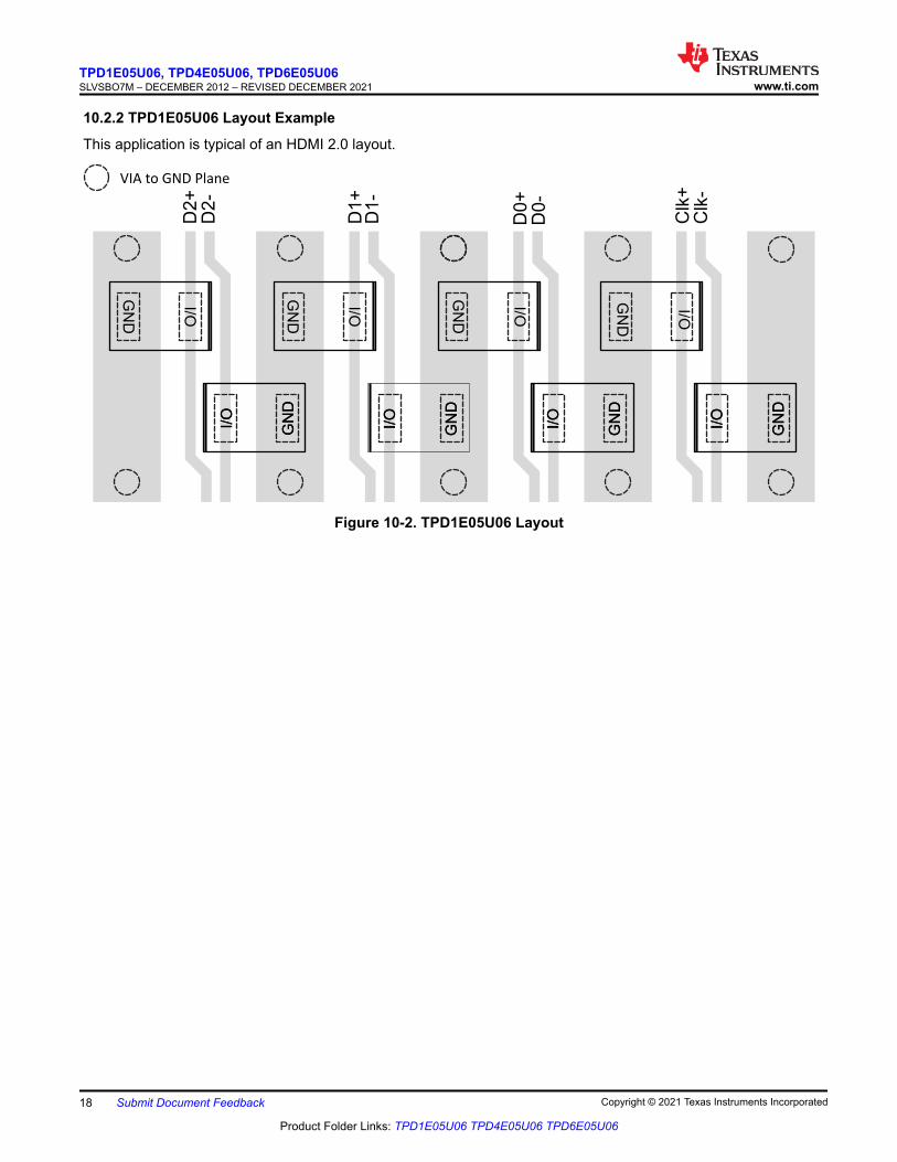
10.2.2 TPD1E05U06 Layout Example
This application is typical of an HDMI 2.0 layout.
Clk
+
Clk
-
D0
+
D0
-
D1
+D
1-
D2
+
D2
-
VIA to GND Plane
I/O
GN
D
I/O
GN
D
I/O
GN
D
I/O
GN
D
I/O
GN
D
I/O
GN
D
I/O
GN
D
I/O
GN
D
I/O
GN
D
I/O
GN
D
I/O
GN
D
I/O
GN
D
Figure 10-2. TPD1E05U06 Layout
TPD1E05U06, TPD4E05U06, TPD6E05U06SLVSBO7M – DECEMBER 2012 – REVISED DECEMBER 2021 www.ti.com
18 Submit Document Feedback Copyright © 2021 Texas Instruments Incorporated
Product Folder Links: TPD1E05U06 TPD4E05U06 TPD6E05U06

11 Device and Documentation Support11.1 Documentation Support11.1.1 Related Documentation
For related documentation, see the following:• Texas Instruments, Reading and Understanding an ESD Protection data sheet• Texas Instruments, ESD Layout Guide application reports• Texas Instruments, TPD6E05U06RVZ EVM user's guide• Texas Instruments, Picking ESD Diodes for Ultra High-Speed Data Lines application reports• Texas Instruments, ESD PROTECTION DIODES EVM user's guide• Texas Instruments, TPD1E05U06DPY EVM user's guide• Texas Instruments, TPD4E05U06DQA EVM user's guide• Texas Instruments, Generic ESD Evaluation Module user's guide
11.2 Receiving Notification of Documentation UpdatesTo receive notification of documentation updates, navigate to the device product folder on ti.com. Click on Subscribe to updates to register and receive a weekly digest of any product information that has changed. For change details, review the revision history included in any revised document.
11.3 Support ResourcesTI E2E™ support forums are an engineer's go-to source for fast, verified answers and design help — straight from the experts. Search existing answers or ask your own question to get the quick design help you need.
Linked content is provided "AS IS" by the respective contributors. They do not constitute TI specifications and do not necessarily reflect TI's views; see TI's Terms of Use.
11.4 TrademarksTI E2E™ is a trademark of Texas Instruments.PCI-express® and PCI-Express® are registered trademarks of PCI-SIG .V-by-One® are registered trademarks of Thine Electronics, Inc.All trademarks are the property of their respective owners.11.5 Electrostatic Discharge Caution
This integrated circuit can be damaged by ESD. Texas Instruments recommends that all integrated circuits be handled with appropriate precautions. Failure to observe proper handling and installation procedures can cause damage.ESD damage can range from subtle performance degradation to complete device failure. Precision integrated circuits may be more susceptible to damage because very small parametric changes could cause the device not to meet its published specifications.
11.6 GlossaryTI Glossary This glossary lists and explains terms, acronyms, and definitions.
12 Mechanical, Packaging, and Orderable InformationThe following pages include mechanical, packaging, and orderable information. This information is the most current data available for the designated devices. This data is subject to change without notice and revision of this document. For browser-based versions of this data sheet, refer to the left-hand navigation.
www.ti.comTPD1E05U06, TPD4E05U06, TPD6E05U06
SLVSBO7M – DECEMBER 2012 – REVISED DECEMBER 2021
Copyright © 2021 Texas Instruments Incorporated Submit Document Feedback 19
Product Folder Links: TPD1E05U06 TPD4E05U06 TPD6E05U06

PACKAGE OPTION ADDENDUM
www.ti.com 11-Nov-2021
Addendum-Page 1
PACKAGING INFORMATION
Orderable Device Status(1)
Package Type PackageDrawing
Pins PackageQty
Eco Plan(2)
Lead finish/Ball material
(6)
MSL Peak Temp(3)
Op Temp (°C) Device Marking(4/5)
Samples
TPD1E05U06DPYR ACTIVE X1SON DPY 2 10000 RoHS & Green NIPDAU Level-1-260C-UNLIM -40 to 125 (BK, C1, C6)C2
TPD1E05U06DPYT ACTIVE X1SON DPY 2 250 RoHS & Green NIPDAU Level-1-260C-UNLIM -40 to 125 (BK, C1, C6)C2
TPD4E05U06DQAR ACTIVE USON DQA 10 3000 RoHS & Green NIPDAU Level-1-260C-UNLIM -40 to 125 (BLG, BRG)BRY
TPD6E05U06RVZR ACTIVE USON RVZ 14 3000 RoHS & Green NIPDAU Level-1-260C-UNLIM -40 to 125 (BV, BVY)
(1) The marketing status values are defined as follows:ACTIVE: Product device recommended for new designs.LIFEBUY: TI has announced that the device will be discontinued, and a lifetime-buy period is in effect.NRND: Not recommended for new designs. Device is in production to support existing customers, but TI does not recommend using this part in a new design.PREVIEW: Device has been announced but is not in production. Samples may or may not be available.OBSOLETE: TI has discontinued the production of the device.
(2) RoHS: TI defines "RoHS" to mean semiconductor products that are compliant with the current EU RoHS requirements for all 10 RoHS substances, including the requirement that RoHS substancedo not exceed 0.1% by weight in homogeneous materials. Where designed to be soldered at high temperatures, "RoHS" products are suitable for use in specified lead-free processes. TI mayreference these types of products as "Pb-Free".RoHS Exempt: TI defines "RoHS Exempt" to mean products that contain lead but are compliant with EU RoHS pursuant to a specific EU RoHS exemption.Green: TI defines "Green" to mean the content of Chlorine (Cl) and Bromine (Br) based flame retardants meet JS709B low halogen requirements of <=1000ppm threshold. Antimony trioxide basedflame retardants must also meet the <=1000ppm threshold requirement.
(3) MSL, Peak Temp. - The Moisture Sensitivity Level rating according to the JEDEC industry standard classifications, and peak solder temperature.
(4) There may be additional marking, which relates to the logo, the lot trace code information, or the environmental category on the device.
(5) Multiple Device Markings will be inside parentheses. Only one Device Marking contained in parentheses and separated by a "~" will appear on a device. If a line is indented then it is a continuationof the previous line and the two combined represent the entire Device Marking for that device.
(6) Lead finish/Ball material - Orderable Devices may have multiple material finish options. Finish options are separated by a vertical ruled line. Lead finish/Ball material values may wrap to twolines if the finish value exceeds the maximum column width.
Important Information and Disclaimer:The information provided on this page represents TI's knowledge and belief as of the date that it is provided. TI bases its knowledge and belief on informationprovided by third parties, and makes no representation or warranty as to the accuracy of such information. Efforts are underway to better integrate information from third parties. TI has taken and

PACKAGE OPTION ADDENDUM
www.ti.com 11-Nov-2021
Addendum-Page 2
continues to take reasonable steps to provide representative and accurate information but may not have conducted destructive testing or chemical analysis on incoming materials and chemicals.TI and TI suppliers consider certain information to be proprietary, and thus CAS numbers and other limited information may not be available for release.
In no event shall TI's liability arising out of such information exceed the total purchase price of the TI part(s) at issue in this document sold by TI to Customer on an annual basis.
OTHER QUALIFIED VERSIONS OF TPD1E05U06, TPD4E05U06 :
• Automotive : TPD1E05U06-Q1, TPD4E05U06-Q1
NOTE: Qualified Version Definitions:
• Automotive - Q100 devices qualified for high-reliability automotive applications targeting zero defects

TAPE AND REEL INFORMATION
*All dimensions are nominal
Device PackageType
PackageDrawing
Pins SPQ ReelDiameter
(mm)
ReelWidth
W1 (mm)
A0(mm)
B0(mm)
K0(mm)
P1(mm)
W(mm)
Pin1Quadrant
TPD1E05U06DPYR X1SON DPY 2 10000 180.0 8.4 0.07 1.1 0.47 2.0 8.0 Q1
TPD1E05U06DPYR X1SON DPY 2 10000 180.0 9.5 0.66 1.15 0.66 2.0 8.0 Q1
TPD1E05U06DPYT X1SON DPY 2 250 180.0 9.5 0.66 1.15 0.66 2.0 8.0 Q1
TPD1E05U06DPYT X1SON DPY 2 250 180.0 8.4 0.07 1.1 0.47 2.0 8.0 Q1
TPD4E05U06DQAR USON DQA 10 3000 180.0 9.5 1.18 2.68 0.72 4.0 8.0 Q1
TPD4E05U06DQAR USON DQA 10 3000 180.0 9.5 1.23 2.7 0.7 4.0 8.0 Q1
TPD4E05U06DQAR USON DQA 10 3000 180.0 8.4 1.23 2.7 0.6 4.0 8.0 Q1
TPD6E05U06RVZR USON RVZ 14 3000 178.0 13.5 1.6 3.75 0.7 4.0 12.0 Q1
TPD6E05U06RVZR USON RVZ 14 3000 180.0 13.2 1.65 3.8 0.7 4.0 12.0 Q1
PACKAGE MATERIALS INFORMATION
www.ti.com 11-Nov-2021
Pack Materials-Page 1

*All dimensions are nominal
Device Package Type Package Drawing Pins SPQ Length (mm) Width (mm) Height (mm)
TPD1E05U06DPYR X1SON DPY 2 10000 203.2 196.8 33.3
TPD1E05U06DPYR X1SON DPY 2 10000 184.0 184.0 19.0
TPD1E05U06DPYT X1SON DPY 2 250 184.0 184.0 19.0
TPD1E05U06DPYT X1SON DPY 2 250 203.2 196.8 33.3
TPD4E05U06DQAR USON DQA 10 3000 189.0 185.0 36.0
TPD4E05U06DQAR USON DQA 10 3000 184.0 184.0 19.0
TPD4E05U06DQAR USON DQA 10 3000 203.2 196.8 33.3
TPD6E05U06RVZR USON RVZ 14 3000 189.0 185.0 36.0
TPD6E05U06RVZR USON RVZ 14 3000 184.0 184.0 19.0
PACKAGE MATERIALS INFORMATION
www.ti.com 11-Nov-2021
Pack Materials-Page 2


www.ti.com
PACKAGE OUTLINE
C0.450.30
0.050.00
0.65
0.1 C A B
2X 0.550.45
2X 0.30.2
A 1.10.9 B
0.70.5
4224561/B 03/2021
X1SON - 0.45 mm max heightDPY0002APLASTIC SMALL OUTLINE - NO LEAD
PIN 1 INDEX AREA
SEATING PLANE
0.08 C
1 2
0.05 C A B
SYMM
SYMM
NOTES: 1. All linear dimensions are in millimeters. Any dimensions in parenthesis are for reference only. Dimensioning and tolerancing per ASME Y14.5M 2. This drawing is subject to change without notice.
SCALE 11.000

www.ti.com
EXAMPLE BOARD LAYOUT
0.07 MINALL AROUND0.07 MAX
ALL AROUND
(R0.05) TYP(0.7)
2X (0.5)
2X (0.3)
4224561/B 03/2021
X1SON - 0.45 mm max heightDPY0002APLASTIC SMALL OUTLINE - NO LEAD
SYMM
1 2
SYMM
LAND PATTERN EXAMPLEEXPOSED METAL SHOWN
SCALE:60X
NOTES: (continued) 3. For more information, see Texas Instruments literature number SLUA271 (www.ti.com/lit/slua271).4. Vias are optional depending on application, refer to device data sheet. If any vias are implemented, refer to their locations shown on this view. It is recommended that vias under paste be filled, plugged or tented.
SOLDER MASK DETAILS
METAL EDGE
SOLDER MASKOPENING
EXPOSEDMETAL
NON SOLDER MASKDEFINED
METAL UNDERSOLDER MASK
SOLDER MASKOPENING
EXPOSEDMETAL
SOLDER MASKDEFINED
(PREFERRED)

www.ti.com
EXAMPLE STENCIL DESIGN
(R0.05) TYP(0.7)
2X (0.5)
2X (0.3) (0)
4224561/B 03/2021
X1SON - 0.45 mm max heightDPY0002APLASTIC SMALL OUTLINE - NO LEAD
NOTES: (continued) 5. Laser cutting apertures with trapezoidal walls and rounded corners may offer better paste release. IPC-7525 may have alternate design recommendations.
SOLDER PASTE EXAMPLEBASED ON 0.1 mm THICK STENCIL
SCALE:60X
SYMM
1 2
SYMM
PCB PAD METALUNDER SOLDER PASTE


www.ti.com
PACKAGE OUTLINE
C
8X 0.250.15
10X 0.430.30
2X2
4X 0.5
0.55 MAX
0.050.00
2X 0.450.35
B 1.10.9
A
2.62.4
(0.13) TYP
(R )0.125
USON - 0.55 mm max heightDQA0010APLASTIC SMALL OUTLINE - NO LEAD
4220328/A 12/2015
PIN 1 INDEX AREA
SEATING PLANE
0.08 C
1
56
10
(OPTIONAL)PIN 1 ID
0.1 C A B0.05 C
0.1 C A B0.05
NOTES: 1. All linear dimensions are in millimeters. Any dimensions in parenthesis are for reference only. Dimensioning and tolerancing per ASME Y14.5M. 2. This drawing is subject to change without notice.
SCALE 6.000

www.ti.com
EXAMPLE BOARD LAYOUT
0.07 MINALL AROUND
0.07 MAXALL AROUND
4X (0.5)
(0.835)
8X (0.2)
10X (0.565)
(R ) TYP0.05
2X (0.4)
USON - 0.55 mm max heightDQA0010APLASTIC SMALL OUTLINE - NO LEAD
4220328/A 12/2015
SYMM
1
56
10
SYMM
LAND PATTERN EXAMPLESCALE:30X
NOTES: (continued) 3. For more information, see Texas Instruments literature number SLUA271 (www.ti.com/lit/slua271).
SOLDER MASKOPENINGSOLDER MASK
METAL UNDER
SOLDER MASKDEFINED
METALSOLDER MASKOPENING
SOLDER MASK DETAILS
NON SOLDER MASKDEFINED
(PREFERRED)

www.ti.com
EXAMPLE STENCIL DESIGN
8X (0.2)
10X (0.565)
4X (0.5)
2X (0.36)
(0.835)
(R ) TYP0.05
USON - 0.55 mm max heightDQA0010APLASTIC SMALL OUTLINE - NO LEAD
4220328/A 12/2015
NOTES: (continued) 4. Laser cutting apertures with trapezoidal walls and rounded corners may offer better paste release. IPC-7525 may have alternate design recommendations.
SOLDER PASTE EXAMPLEBASED ON 0.1 mm THICK STENCIL
EXPOSED PADS 3 & 8:
90% PRINTED SOLDER COVERAGE BY AREA UNDER PACKAGESCALE:40X
SYMM
1
56
10
SYMM
METALTYP
3 8

IMPORTANT NOTICE AND DISCLAIMERTI PROVIDES TECHNICAL AND RELIABILITY DATA (INCLUDING DATA SHEETS), DESIGN RESOURCES (INCLUDING REFERENCE DESIGNS), APPLICATION OR OTHER DESIGN ADVICE, WEB TOOLS, SAFETY INFORMATION, AND OTHER RESOURCES “AS IS” AND WITH ALL FAULTS, AND DISCLAIMS ALL WARRANTIES, EXPRESS AND IMPLIED, INCLUDING WITHOUT LIMITATION ANY IMPLIED WARRANTIES OF MERCHANTABILITY, FITNESS FOR A PARTICULAR PURPOSE OR NON-INFRINGEMENT OF THIRD PARTY INTELLECTUAL PROPERTY RIGHTS.These resources are intended for skilled developers designing with TI products. You are solely responsible for (1) selecting the appropriate TI products for your application, (2) designing, validating and testing your application, and (3) ensuring your application meets applicable standards, and any other safety, security, regulatory or other requirements.These resources are subject to change without notice. TI grants you permission to use these resources only for development of an application that uses the TI products described in the resource. Other reproduction and display of these resources is prohibited. No license is granted to any other TI intellectual property right or to any third party intellectual property right. TI disclaims responsibility for, and you will fully indemnify TI and its representatives against, any claims, damages, costs, losses, and liabilities arising out of your use of these resources.TI’s products are provided subject to TI’s Terms of Sale or other applicable terms available either on ti.com or provided in conjunction with such TI products. TI’s provision of these resources does not expand or otherwise alter TI’s applicable warranties or warranty disclaimers for TI products.TI objects to and rejects any additional or different terms you may have proposed. IMPORTANT NOTICE
Mailing Address: Texas Instruments, Post Office Box 655303, Dallas, Texas 75265Copyright © 2021, Texas Instruments Incorporated