esd351 1-channel 30 kv esd protection diode with low
TRANSCRIPT
5-V Source
USB Transceiver
2
1
2
1
ES
D35
1
ES
D35
1
VBUS
D±
D+
GND
Product
Folder
Order
Now
Technical
Documents
Tools &
Software
Support &Community
An IMPORTANT NOTICE at the end of this data sheet addresses availability, warranty, changes, use in safety-critical applications,intellectual property matters and other important disclaimers. PRODUCTION DATA.
ESD351SLVSEO3 –JULY 2018
ESD351 1-Channel 30 kV ESD Protection Diode with Low Clamping Voltage in0402 Package
1
1 Features1• IEC 61000-4-2 Level 4 ESD Protection
– ±30-kV Contact Discharge– ±30-kV Air Gap Discharge
• IEC 61000-4-4 EFT Protection– 80 A (5/50 ns)
• IEC 61000-4-5 Surge Protection– 6 A (8/20 µs)
• IO Capacitance: 1.8 pF (Typical)• DC Breakdown Voltage: 4.5 V (Minimum)• Low Leakage Current: 0.1 nA (Typical)• Extremely Low ESD Clamping Voltage
– 6.5 V at 16-A TLP (I/O Pin to GND)– RDYN: 0.1 Ω (I/O Pin to GND)
• Industrial Temperature Range: –40°C to +125°C• Industry Standard 0402 Package (DFN1006P2)
2 Applications• End Equipment
– Wearables– Industrial and Service Robots– Laptops and Desktops– Mobile and Tablets– Set-Top Boxes– DVR and NVR– TV and Monitors– EPOS (Electronic Point of Sale)
• Interfaces– USB 2.0/1.1– GPIO– Pushbuttons– Audio
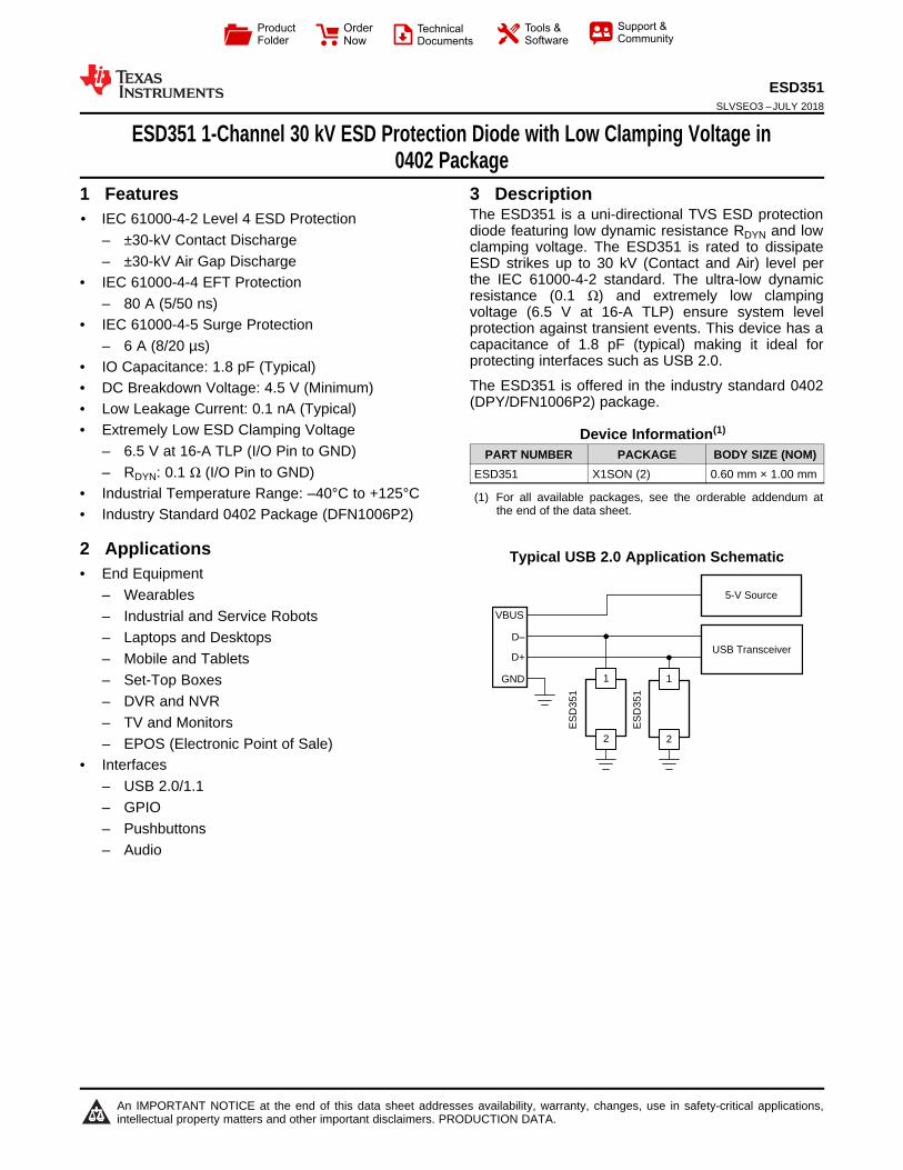
3 DescriptionThe ESD351 is a uni-directional TVS ESD protectiondiode featuring low dynamic resistance RDYN and lowclamping voltage. The ESD351 is rated to dissipateESD strikes up to 30 kV (Contact and Air) level perthe IEC 61000-4-2 standard. The ultra-low dynamicresistance (0.1 Ω) and extremely low clampingvoltage (6.5 V at 16-A TLP) ensure system levelprotection against transient events. This device has acapacitance of 1.8 pF (typical) making it ideal forprotecting interfaces such as USB 2.0.
The ESD351 is offered in the industry standard 0402(DPY/DFN1006P2) package.
Device Information(1)
PART NUMBER PACKAGE BODY SIZE (NOM)ESD351 X1SON (2) 0.60 mm × 1.00 mm
(1) For all available packages, see the orderable addendum atthe end of the data sheet.
Typical USB 2.0 Application Schematic

2
ESD351SLVSEO3 –JULY 2018 www.ti.com
Product Folder Links: ESD351
Submit Documentation Feedback Copyright © 2018, Texas Instruments Incorporated
Table of Contents1 Features .................................................................. 12 Applications ........................................................... 13 Description ............................................................. 14 Revision History..................................................... 25 Pin Configuration and Functions ......................... 36 Specifications......................................................... 4
6.1 Absolute Maximum Ratings ...................................... 46.2 ESD Ratings -JEDEC Specifications ........................ 46.3 ESD Ratings - IEC Specifications............................. 46.4 Recommended Operating Conditions....................... 46.5 Thermal Information .................................................. 46.6 Electrical Characteristics........................................... 56.7 Typical Characteristics .............................................. 6
7 Detailed Description .............................................. 87.1 Overview ................................................................... 87.2 Functional Block Diagram ......................................... 87.3 Feature Description................................................... 8
7.4 Device Functional Modes.......................................... 88 Application and Implementation .......................... 9
8.1 Application Information.............................................. 98.2 Typical Application ................................................... 9
9 Power Supply Recommendations ...................... 1110 Layout................................................................... 11
10.1 Layout Guidelines ................................................. 1110.2 Layout Example .................................................... 11
11 Device and Documentation Support ................. 1211.1 Documentation Support ........................................ 1211.2 Receiving Notification of Documentation Updates 1211.3 Community Resources.......................................... 1211.4 Trademarks ........................................................... 1211.5 Electrostatic Discharge Caution............................ 1211.6 Glossary ................................................................ 12
12 Mechanical, Packaging, and OrderableInformation ........................................................... 12
4 Revision History
DATE REVISION NOTESJuly 2018 * Initial release.

1
2
3
ESD351www.ti.com SLVSEO3 –JULY 2018
Product Folder Links: ESD351
Submit Documentation FeedbackCopyright © 2018, Texas Instruments Incorporated
5 Pin Configuration and Functions
DPY Package2-Pin X1SON
Top View
Pin FunctionsPIN
I/O DESCRIPTIONNO. NAME
1 IO I/O ESD Protected Channel. Connect this pin to the line being protected.2 GND GND Connect this pin to Ground

4
ESD351SLVSEO3 –JULY 2018 www.ti.com
Product Folder Links: ESD351
Submit Documentation Feedback Copyright © 2018, Texas Instruments Incorporated
(1) Stresses beyond those listed under Absolute Maximum Rating may cause permanent damage to the device. These are stress ratingsonly, which do not imply functional operation of the device at these or any other conditions beyond those indicated under RecommendedOperating Condition. Exposure to absolute-maximum-rated conditions for extended periods may affect device reliability.
6 Specifications
6.1 Absolute Maximum Ratingsover operating free-air temperature range (unless otherwise noted) (1)
MIN MAX UNITElectrical FastTransient IEC 61000-4-4 Peak Current at 25 °C 80 A
Surge PulseIEC 61000-4-5 Surge (tp 8/20 µs) Peak Power at 25 °C 36 WIEC 61000-4-5 Surge (tp 8/20 µs) Peak Current at 25 °C 6 A
TA Operating free-air temperature –40 125 °CTstg Storage temperature –65 155 °C
(1) JEDEC document JEP155 states that 500-V HBM allows safe manufacturing with a standard ESD control process.(2) JEDEC document JEP157 states that 250-V CDM allows safe manufacturing with a standard ESD control process.
6.2 ESD Ratings -JEDEC SpecificationsVALUE UNIT
V(ESD) Electrostatic discharge
Human body model (HBM), perANSI/ESDA/JEDEC JS-001, allpins (1) ±2500
VCharged device model (CDM), per JEDECspecificationJESD22-C101, all pins (2) ±1000
6.3 ESD Ratings - IEC SpecificationsVALUE UNIT
V(ESD) Electrostatic dischargeIEC 61000-4-2 Contact Discharge, all pins ±30000
VIEC 61000-4-2 Air Discharge, all pins ±30000
6.4 Recommended Operating Conditionsover operating free-air temperature range (unless otherwise noted)
MIN NOM MAX UNITVIN Input voltage 0 3.6 VTA Operating Free Air Temperature –40 125 °C
(1) For more information about traditional and new thermal metrics, see the Semiconductor and IC Package Thermal Metrics applicationreport.
6.5 Thermal Information
THERMAL METRIC (1)ESD351
UNITDPY (X1SON)2 PINS
RθJA Junction-to-ambient thermal resistance 409.4 °C/WRθJC(top) Junction-to-case (top) thermal resistance 216.8 °C/WRθJB Junction-to-board thermal resistance 140.4 °C/WΨJT Junction-to-top characterization parameter 81.4 °C/WΨJB Junction-to-board characterization parameter 140.0 °C/WRθJC(bot) Junction-to-case (bottom) thermal resistance N/A °C/W

5
ESD351www.ti.com SLVSEO3 –JULY 2018
Product Folder Links: ESD351
Submit Documentation FeedbackCopyright © 2018, Texas Instruments Incorporated
(1) VBRF and VBRR are defined as the voltage obtained at 1 mA when sweeping the voltage up, before the device latches into the snapbackstate
(2) VHOLD is defined as the voltage when 1 mA is applied, after the device has successfully latched into the snapback state.
6.6 Electrical CharacteristicsAt TA = 25°C unless otherwise noted
PARAMETER TEST CONDITIONS MIN TYP MAX UNIT
VRWM Reverse stand-off voltage IIO < 50 nA, across operatingtemperature range 3.6 V
ILEAKAGE Leakage current at 3.6 V VIO = 3.6 V, I/O to GND 0.1 10 nAVBRF Breakdown voltage, I/O to GND (1) IIO = 1 mA 4.5 7.5 VVFWD Forward Voltage, GND to I/O (1) IIO = 1 mA 0.8 VVHOLD Holding voltage, I/O to GND (2) IIO = 1 mA 5.1 V
VCLAMP Clamping voltageIPP = 6 A (8/20 µs Surge), I/O to GND 6.1 VIPP = 16 A (100 ns TLP), I/O to GND 6.5 VIPP = 16 A (100 ns TLP), GND to I/O 2.5 V
RDYN Dynamic resistance
I/O to GND, 100 ns TLP, between 10to 20 A IPP
0.1Ω
GND to I/O , 100 ns TLP, between 10to 20 A IPP
0.08
CLINE Line capacitance, IO to GND VIO = 0 V, Vp-p = 30 mV, f = 1 MHz 1.8 2.2 pF

D007_Leakage.grf
Temperature (°C)
Cur
rent
(nA
)
-40 -20 0 20 40 60 80 100 120 1400
0.5
1
1.5
2
2.5
3
3.5
D007
D008_Cap.grf
Bias Voltage (V)
Cap
acita
nce
(pF
)
0 0.4 0.8 1.2 1.6 2 2.4 2.8 3.2 3.6 40.4
0.8
1.2
1.6
2
2.4
2.8
3.2
D008
-402585125
D005_Surge.grf
Time (Ps)
Cur
rent
(A
), P
ower
(W
)
-20 0 20 40 60 80 100 120 140 160 180-5
0
5
10
15
20
25
30
35
40
45
D005
Current (A)Power (W)
D006_DC.grf
Voltage (V)
Cur
rent
(A
)
-1 0 1 2 3 4 5 6 7-0.001
-0.0008
-0.0006
-0.0004
-0.0002
0
0.0002
0.0004
0.0006
0.0008
0.001
D006
D003_Positive_IEC.grf
Time (ns)
Vol
tage
(V
)
-10 0 10 20 30 40 50 60 70 80 90-5
0
5
10
15
20
25
30
35
40
D003
D004_Negative_IEC.grf
Time (ns)
Vol
tage
(V
)
-10 0 10 20 30 40 50 60 70 80 90-30
-25
-20
-15
-10
-5
0
5
D004
D001_Positive_TLP.grf
Voltage (V)
Cur
rent
(A
)
0 1 2 3 4 5 6 7 8-4
0
4
8
12
16
20
24
28
32
D001
D002_Negative_TLP.grf
Voltage (V)
Cur
rent
(A
)
-4 -3.5 -3 -2.5 -2 -1.5 -1 -0.5 0-32
-28
-24
-20
-16
-12
-8
-4
0
4
D002
6
ESD351SLVSEO3 –JULY 2018 www.ti.com
Product Folder Links: ESD351
Submit Documentation Feedback Copyright © 2018, Texas Instruments Incorporated
6.7 Typical Characteristics
Figure 1. TLP I-V Curve, I/O Pin to GND (tp = 100 ns) Figure 2. TLP I/V Curve, GND to I/O Pin (tp = 100 ns)
Figure 3. 8-kV IEC 61000-4-2 Clamping Voltage, I/O pin toGND
Figure 4. 8-kV IEC 61000-4-2 Clamping Voltage, GND to I/OPin
Figure 5. Surge Curve (IEC 61000-4-5, tp = 8/20 µs), I/O Pinto GND
Figure 6. DC IV-Curve, I/O Pin to GND
Figure 7. Leakage Current at 3.6 V Bias Voltage AcrossTemperature, I/O Pin to GND
Figure 8. Capacitance Vs. Bias Voltage at DifferentTemperatures (°C)
D009_InsertionLoss.grf
Frequency (GHz)
S21
(dB
)
0.1 0.2 0.3 0.4 0.5 0.7 1 2 3 4 55-7
-6
-5
-4
-3
-2
-1
0
D009
7
ESD351www.ti.com SLVSEO3 –JULY 2018
Product Folder Links: ESD351
Submit Documentation FeedbackCopyright © 2018, Texas Instruments Incorporated
Typical Characteristics (continued)
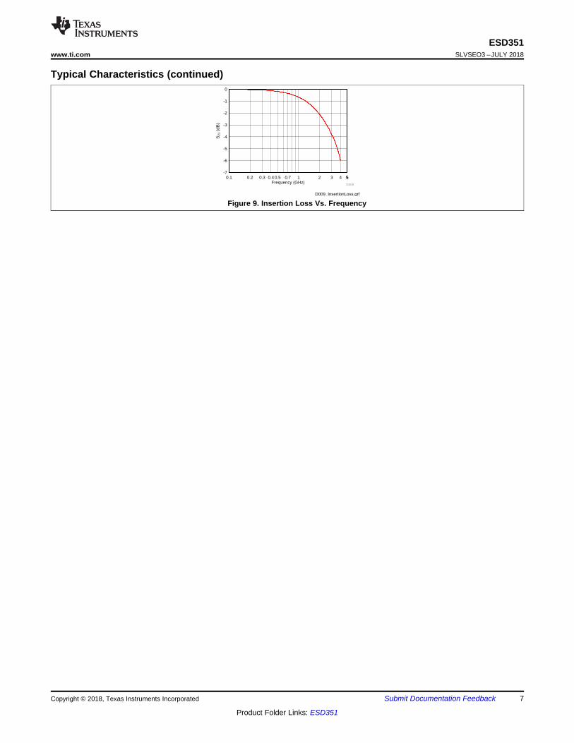
Figure 9. Insertion Loss Vs. Frequency

8
ESD351SLVSEO3 –JULY 2018 www.ti.com
Product Folder Links: ESD351
Submit Documentation Feedback Copyright © 2018, Texas Instruments Incorporated
7 Detailed Description
7.1 OverviewThe ESD351 is a uni-directional ESD Protection Diode with 30 kV IEC 61000-4-2 level (Contact and Air) withultra-low clamping voltage in a 1 mm × 0.6 mm package. The ultra-low clamping makes this device capable ofprotecting any ESD-sensitive pins.
7.2 Functional Block Diagram
7.3 Feature DescriptionESD351 provides ESD protection up to ±30-kV contact and ±30-kV air gap per IEC 61000-4-2 standard. Duringan ESD event, ESD diode connected to the I/O pin turns on and diverts the current to ground. Additionally,ESD351 also provides protection against IEC 61000-4-5 Surge currents up to 6 A (8/20µs waveform) and up to80 A per IEC 61000-4-4 (5/50 ns waveform, 4 kV with 50-Ω impedance) electrical fast transient (EFT) standard.The capacitance between the I/O pin and ground is 1.8 pF (typical) and 2.2 pF (maximum). The device featuresa low leakage current of 0.1 nA (typical) and 50 nA (maximum, across operating temperature range) with a biasof 3.6 V. The ESD diode at the I/O pin protects the ESD-sensitive devices by clamping the voltage to a low valueof 6.5 V (IPP = 16 A 100 ns TLP ). The layout of this device makes it simple and easy to add protection to anexisting layout. The packages offers flow-through routing, requiring minimal modification to an existing layout.
7.4 Device Functional ModesThe ESD351 is a passive integrated circuit that triggers when voltages are above VBRF or below VFWD. DuringESD events, voltages as high as ±30 kV (contact or air) can be directed to ground via the internal diode network.When the voltages on the protected line fall below the trigger levels of ESD351 (usually within 10s of nano-seconds) the device reverts to passive.
5-V Source
USB Transceiver
2
1
2
1
ES
D35
1
ES
D35
1
VBUS
D±
D+
GND
9
ESD351www.ti.com SLVSEO3 –JULY 2018
Product Folder Links: ESD351
Submit Documentation FeedbackCopyright © 2018, Texas Instruments Incorporated
8 Application and Implementation
NOTEInformation in the following applications sections is not part of the TI componentspecification, and TI does not warrant its accuracy or completeness. TI’s customers areresponsible for determining suitability of components for their purposes. Customers shouldvalidate and test their design implementation to confirm system functionality.
8.1 Application InformationThe ESD351 is a diode type TVS which is used to provide a path to ground for dissipating ESD events on high-speed signal lines between a human interface connector and a system. As the current from ESD passes throughthe TVS, only a small voltage drop is present across the diode. This is the voltage presented to the protected IC.The low RDYN of the triggered TVS holds this voltage, VCLAMP, to a safe level for the protected IC.
8.2 Typical Application
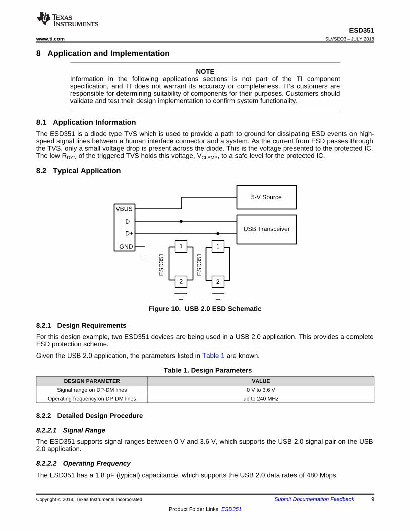
Figure 10. USB 2.0 ESD Schematic
8.2.1 Design RequirementsFor this design example, two ESD351 devices are being used in a USB 2.0 application. This provides a completeESD protection scheme.
Given the USB 2.0 application, the parameters listed in Table 1 are known.
Table 1. Design ParametersDESIGN PARAMETER VALUE
Signal range on DP-DM lines 0 V to 3.6 VOperating frequency on DP-DM lines up to 240 MHz
8.2.2 Detailed Design Procedure
8.2.2.1 Signal RangeThe ESD351 supports signal ranges between 0 V and 3.6 V, which supports the USB 2.0 signal pair on the USB2.0 application.
8.2.2.2 Operating FrequencyThe ESD351 has a 1.8 pF (typical) capacitance, which supports the USB 2.0 data rates of 480 Mbps.

D009_InsertionLoss.grf
Frequency (GHz)
S21
(dB
)
0.1 0.2 0.3 0.4 0.5 0.7 1 2 3 4 55-7
-6
-5
-4
-3
-2
-1
0
D009
10
ESD351SLVSEO3 –JULY 2018 www.ti.com
Product Folder Links: ESD351
Submit Documentation Feedback Copyright © 2018, Texas Instruments Incorporated
8.2.3 Application Curve
Figure 11. Insertion Loss

USB2.0 Connector
Pin to GND
Legend
GND
VBUS To power supply
To USB transceiver
D+
D-ESD351
ESD351
11
ESD351www.ti.com SLVSEO3 –JULY 2018
Product Folder Links: ESD351
Submit Documentation FeedbackCopyright © 2018, Texas Instruments Incorporated
9 Power Supply RecommendationsThe ESD351 is a passive ESD device so there is no need to power it. Take care not to violate the recommendedI/O specification (0 V to 3.6 V) to ensure the device functions properly.
10 Layout
10.1 Layout Guidelines• The optimum placement is as close to the connector as possible.
– EMI during an ESD event can couple from the trace being struck to other nearby unprotected traces,resulting in early system failures.
– The PCB designer must minimize the possibility of EMI coupling by keeping any unprotected traces awayfrom the protected traces which are between the TVS and the connector.
• Route the protected traces as straight as possible.• Eliminate any sharp corners on the protected traces between the TVS and the connector by using rounded
corners with the largest radii possible.– Electric fields tend to build up on corners, increasing EMI coupling.
10.2 Layout Example
Figure 12. USB 2.0 ESD Layout

12
ESD351SLVSEO3 –JULY 2018 www.ti.com
Product Folder Links: ESD351
Submit Documentation Feedback Copyright © 2018, Texas Instruments Incorporated
11 Device and Documentation Support
11.1 Documentation Support
11.1.1 Related DocumentationFor related documentation see the following:
Generic ESD Device Evaluation Module, SLVUBG5
11.2 Receiving Notification of Documentation UpdatesTo receive notification of documentation updates, navigate to the device product folder on ti.com. In the upperright corner, click on Alert me to register and receive a weekly digest of any product information that haschanged. For change details, review the revision history included in any revised document.
11.3 Community ResourcesThe following links connect to TI community resources. Linked contents are provided "AS IS" by the respectivecontributors. They do not constitute TI specifications and do not necessarily reflect TI's views; see TI's Terms ofUse.
TI E2E™ Online Community TI's Engineer-to-Engineer (E2E) Community. Created to foster collaborationamong engineers. At e2e.ti.com, you can ask questions, share knowledge, explore ideas and helpsolve problems with fellow engineers.
Design Support TI's Design Support Quickly find helpful E2E forums along with design support tools andcontact information for technical support.
11.4 TrademarksE2E is a trademark of Texas Instruments.All other trademarks are the property of their respective owners.
11.5 Electrostatic Discharge CautionThis integrated circuit can be damaged by ESD. Texas Instruments recommends that all integrated circuits be handled withappropriate precautions. Failure to observe proper handling and installation procedures can cause damage.
ESD damage can range from subtle performance degradation to complete device failure. Precision integrated circuits may be moresusceptible to damage because very small parametric changes could cause the device not to meet its published specifications.
11.6 GlossarySLYZ022 — TI Glossary.
This glossary lists and explains terms, acronyms, and definitions.
12 Mechanical, Packaging, and Orderable InformationThe following pages include mechanical, packaging, and orderable information. This information is the mostcurrent data available for the designated devices. This data is subject to change without notice and revision ofthis document. For browser-based versions of this data sheet, refer to the left-hand navigation.
PACKAGE OPTION ADDENDUM
www.ti.com 10-Dec-2020
Addendum-Page 1
PACKAGING INFORMATION
Orderable Device Status(1)
Package Type PackageDrawing
Pins PackageQty
Eco Plan(2)
Lead finish/Ball material
(6)
MSL Peak Temp(3)
Op Temp (°C) Device Marking(4/5)
Samples
ESD351DPYR ACTIVE X1SON DPY 2 10000 RoHS & Green NIPDAU Level-1-260C-UNLIM -40 to 125 DE
(1) The marketing status values are defined as follows:ACTIVE: Product device recommended for new designs.LIFEBUY: TI has announced that the device will be discontinued, and a lifetime-buy period is in effect.NRND: Not recommended for new designs. Device is in production to support existing customers, but TI does not recommend using this part in a new design.PREVIEW: Device has been announced but is not in production. Samples may or may not be available.OBSOLETE: TI has discontinued the production of the device.
(2) RoHS: TI defines "RoHS" to mean semiconductor products that are compliant with the current EU RoHS requirements for all 10 RoHS substances, including the requirement that RoHS substancedo not exceed 0.1% by weight in homogeneous materials. Where designed to be soldered at high temperatures, "RoHS" products are suitable for use in specified lead-free processes. TI mayreference these types of products as "Pb-Free".RoHS Exempt: TI defines "RoHS Exempt" to mean products that contain lead but are compliant with EU RoHS pursuant to a specific EU RoHS exemption.Green: TI defines "Green" to mean the content of Chlorine (Cl) and Bromine (Br) based flame retardants meet JS709B low halogen requirements of <=1000ppm threshold. Antimony trioxide basedflame retardants must also meet the <=1000ppm threshold requirement.
(3) MSL, Peak Temp. - The Moisture Sensitivity Level rating according to the JEDEC industry standard classifications, and peak solder temperature.
(4) There may be additional marking, which relates to the logo, the lot trace code information, or the environmental category on the device.
(5) Multiple Device Markings will be inside parentheses. Only one Device Marking contained in parentheses and separated by a "~" will appear on a device. If a line is indented then it is a continuationof the previous line and the two combined represent the entire Device Marking for that device.
(6) Lead finish/Ball material - Orderable Devices may have multiple material finish options. Finish options are separated by a vertical ruled line. Lead finish/Ball material values may wrap to twolines if the finish value exceeds the maximum column width.
Important Information and Disclaimer:The information provided on this page represents TI's knowledge and belief as of the date that it is provided. TI bases its knowledge and belief on informationprovided by third parties, and makes no representation or warranty as to the accuracy of such information. Efforts are underway to better integrate information from third parties. TI has taken andcontinues to take reasonable steps to provide representative and accurate information but may not have conducted destructive testing or chemical analysis on incoming materials and chemicals.TI and TI suppliers consider certain information to be proprietary, and thus CAS numbers and other limited information may not be available for release.
In no event shall TI's liability arising out of such information exceed the total purchase price of the TI part(s) at issue in this document sold by TI to Customer on an annual basis.
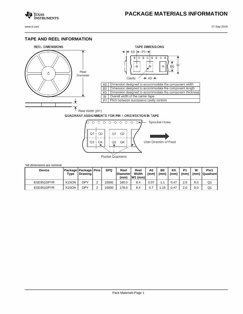
TAPE AND REEL INFORMATION
*All dimensions are nominal
Device PackageType
PackageDrawing
Pins SPQ ReelDiameter
(mm)
ReelWidth
W1 (mm)
A0(mm)
B0(mm)
K0(mm)
P1(mm)
W(mm)
Pin1Quadrant
ESD351DPYR X1SON DPY 2 10000 180.0 8.4 0.07 1.1 0.47 2.0 8.0 Q1
ESD351DPYR X1SON DPY 2 10000 178.0 8.4 0.7 1.15 0.47 2.0 8.0 Q1
PACKAGE MATERIALS INFORMATION
www.ti.com 27-Sep-2019
Pack Materials-Page 1
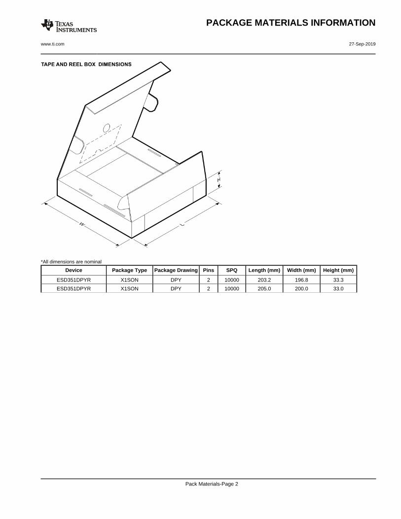
*All dimensions are nominal
Device Package Type Package Drawing Pins SPQ Length (mm) Width (mm) Height (mm)
ESD351DPYR X1SON DPY 2 10000 203.2 196.8 33.3
ESD351DPYR X1SON DPY 2 10000 205.0 200.0 33.0
PACKAGE MATERIALS INFORMATION
www.ti.com 27-Sep-2019
Pack Materials-Page 2


www.ti.com
PACKAGE OUTLINE
C0.450.30
0.050.00
0.65
0.1 C A B
2X 0.550.45
2X 0.30.2
A 1.10.9 B
0.70.5
4224561/B 03/2021
X1SON - 0.45 mm max heightDPY0002APLASTIC SMALL OUTLINE - NO LEAD
PIN 1 INDEX AREA
SEATING PLANE
0.08 C
1 2
0.05 C A B
SYMM
SYMM
NOTES: 1. All linear dimensions are in millimeters. Any dimensions in parenthesis are for reference only. Dimensioning and tolerancing per ASME Y14.5M 2. This drawing is subject to change without notice.
SCALE 11.000

www.ti.com
EXAMPLE BOARD LAYOUT
0.07 MINALL AROUND0.07 MAX
ALL AROUND
(R0.05) TYP(0.7)
2X (0.5)
2X (0.3)
4224561/B 03/2021
X1SON - 0.45 mm max heightDPY0002APLASTIC SMALL OUTLINE - NO LEAD
SYMM
1 2
SYMM
LAND PATTERN EXAMPLEEXPOSED METAL SHOWN
SCALE:60X
NOTES: (continued) 3. For more information, see Texas Instruments literature number SLUA271 (www.ti.com/lit/slua271).4. Vias are optional depending on application, refer to device data sheet. If any vias are implemented, refer to their locations shown on this view. It is recommended that vias under paste be filled, plugged or tented.
SOLDER MASK DETAILS
METAL EDGE
SOLDER MASKOPENING
EXPOSEDMETAL
NON SOLDER MASKDEFINED
METAL UNDERSOLDER MASK
SOLDER MASKOPENING
EXPOSEDMETAL
SOLDER MASKDEFINED
(PREFERRED)

www.ti.com
EXAMPLE STENCIL DESIGN
(R0.05) TYP(0.7)
2X (0.5)
2X (0.3) (0)
4224561/B 03/2021
X1SON - 0.45 mm max heightDPY0002APLASTIC SMALL OUTLINE - NO LEAD
NOTES: (continued) 5. Laser cutting apertures with trapezoidal walls and rounded corners may offer better paste release. IPC-7525 may have alternate design recommendations.
SOLDER PASTE EXAMPLEBASED ON 0.1 mm THICK STENCIL
SCALE:60X
SYMM
1 2
SYMM
PCB PAD METALUNDER SOLDER PASTE

IMPORTANT NOTICE AND DISCLAIMERTI PROVIDES TECHNICAL AND RELIABILITY DATA (INCLUDING DATASHEETS), DESIGN RESOURCES (INCLUDING REFERENCEDESIGNS), APPLICATION OR OTHER DESIGN ADVICE, WEB TOOLS, SAFETY INFORMATION, AND OTHER RESOURCES “AS IS”AND WITH ALL FAULTS, AND DISCLAIMS ALL WARRANTIES, EXPRESS AND IMPLIED, INCLUDING WITHOUT LIMITATION ANYIMPLIED WARRANTIES OF MERCHANTABILITY, FITNESS FOR A PARTICULAR PURPOSE OR NON-INFRINGEMENT OF THIRDPARTY INTELLECTUAL PROPERTY RIGHTS.These resources are intended for skilled developers designing with TI products. You are solely responsible for (1) selecting the appropriateTI products for your application, (2) designing, validating and testing your application, and (3) ensuring your application meets applicablestandards, and any other safety, security, or other requirements. These resources are subject to change without notice. TI grants youpermission to use these resources only for development of an application that uses the TI products described in the resource. Otherreproduction and display of these resources is prohibited. No license is granted to any other TI intellectual property right or to any third partyintellectual property right. TI disclaims responsibility for, and you will fully indemnify TI and its representatives against, any claims, damages,costs, losses, and liabilities arising out of your use of these resources.TI’s products are provided subject to TI’s Terms of Sale (https:www.ti.com/legal/termsofsale.html) or other applicable terms available eitheron ti.com or provided in conjunction with such TI products. TI’s provision of these resources does not expand or otherwise alter TI’sapplicable warranties or warranty disclaimers for TI products.IMPORTANT NOTICE
Mailing Address: Texas Instruments, Post Office Box 655303, Dallas, Texas 75265Copyright © 2021, Texas Instruments Incorporated