total ionizing dose test report no. 13t-rtax2000s-cq352 …
TRANSCRIPT

Total Ionizing Dose Test Report No. 19T-RTAX2000S-CQ352-DFAWC1
September 13, 2019

Total Ionizing Dose Test Report Rev. 0 No. 19T-RTAX2000S-CQ352-DFAWC1
Page 2 of 56 1-06-12020 rev 0
Table of Contents I. Summary Table ........................................................................................................... 3
II. Total Ionizing Dose (TID) Testing ............................................................................. 3 A. Device-Under-Test (DUT) and Irradiation Parameters ................................................................ 3 B. Test Method .............................................................................................................................. 4 C. Design and Parametric Measurements....................................................................................... 5
III. Test Results ................................................................................................................ 6 A. Functionality .............................................................................................................................. 6 B. Power Supply Current (ICCA and ICCI) ..................................................................................... 6 C. Single-Ended Input Logic Threshold (VIL/VIH) ......................................................................... 10 D. Differential Input (LVPECL) Threshold Voltage (VIL/VIH) .......................................................... 11 E. Output-Drive Voltage (VOL/VOH)............................................................................................. 12 F. Propagation Delay ................................................................................................................... 13 G. Transition Characteristics ........................................................................................................ 15
Appendix A: DUT Bias ..................................................................................................... 27
Appendix B: DUT Design Schematics and Verilog Files ............................................ 29
Total Ionizing Dose Test Report Rev. 0 No. 19T-RTAX2000S-CQ352-DFAWC1
Page 3 of 56 1-06-12020 rev 0
TOTAL IONIZING DOSE TEST REPORT
No. 19T-RTAX2000S-CQ352-DFAWC1 August 27, 2019
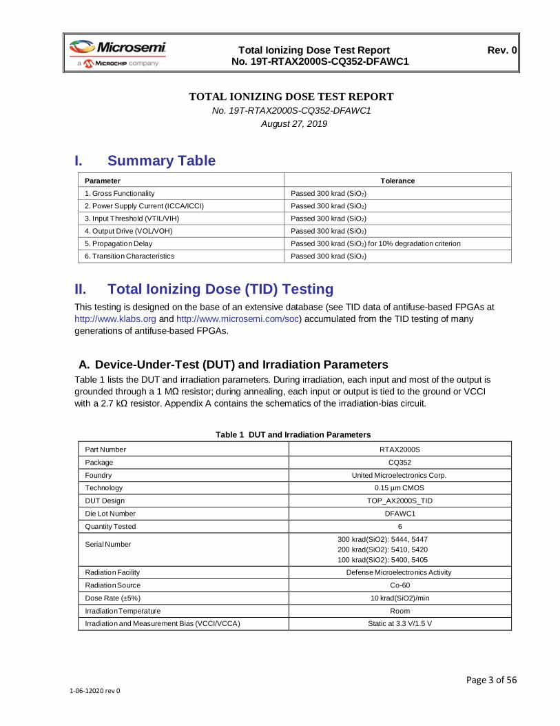
I. Summary Table
Parameter Tolerance
1. Gross Functionality Passed 300 krad (SiO2)
2. Power Supply Current (ICCA/ICCI) Passed 300 krad (SiO2)
3. Input Threshold (VTIL/VIH) Passed 300 krad (SiO2)
4. Output Drive (VOL/VOH) Passed 300 krad (SiO2)
5. Propagation Delay Passed 300 krad (SiO2) for 10% degradation criterion
6. Transition Characteristics Passed 300 krad (SiO2)
II. Total Ionizing Dose (TID) Testing This testing is designed on the base of an extensive database (see TID data of antifuse-based FPGAs at http://www.klabs.org and http://www.microsemi.com/soc) accumulated from the TID testing of many generations of antifuse-based FPGAs.
A. Device-Under-Test (DUT) and Irradiation Parameters Table 1 lists the DUT and irradiation parameters. During irradiation, each input and most of the output is grounded through a 1 MΩ resistor; during annealing, each input or output is tied to the ground or VCCI with a 2.7 kΩ resistor. Appendix A contains the schematics of the irradiation-bias circuit.
Table 1 DUT and Irradiation Parameters
Part Number RTAX2000S
Package CQ352
Foundry United Microelectronics Corp.
Technology 0.15 µm CMOS
DUT Design TOP_AX2000S_TID
Die Lot Number DFAWC1
Quantity Tested 6
Serial Number 300 krad(SiO2): 5444, 5447 200 krad(SiO2): 5410, 5420 100 krad(SiO2): 5400, 5405
Radiation Facility Defense Microelectronics Activity
Radiation Source Co-60
Dose Rate (±5%) 10 krad(SiO2)/min
Irradiation Temperature Room
Irradiation and Measurement Bias (VCCI/VCCA) Static at 3.3 V/1.5 V

Total Ionizing Dose Test Report Rev. 0 No. 19T-RTAX2000S-CQ352-DFAWC1
Page 4 of 56 1-06-12020 rev 0
B. Test Method
Figure 1 Parametric Test Flow Chart
The test method generally follows the guidelines in the military standard TM1019.8. Figure 1 is the flow chart describing the steps for functional and parametric tests, irradiation, and post-irradiation annealing.
The accelerated aging, or rebound test mentioned in TM1019.8, is unnecessary; because there is no adverse time-dependent effect (TDE) in Microsemi products manufactured by deep sub-micron CMOS technologies. Elevated temperature annealing basically reduces the effects originating from radiation- induced leakage currents. As indicated by test data in the following sections, the predominant radiation effects in RTAX2000S are due to radiation-induced leakage currents.
Room temperature annealing is performed in this test; the duration is approximately 7 days.

Total Ionizing Dose Test Report Rev. 0 No. 19T-RTAX2000S-CQ352-DFAWC1
Page 5 of 56 1-06-12020 rev 0
C. Design and Parametric Measurements The DUT uses a high utilization, generic design (TOP_AX2000S_TID) to evaluate total dose effects for typical space applications. Appendix B contains the schematics and Verilog files of this design.
Table 2 lists measured electrical parameters and the corresponding logic design. The functionality is measured on the output pin (O_BS) of a combinational buffer-string with 14,000 buffers, output pins (O_ANDP_CLKF, O_ORP_CLKF, O_FF_CLKF, O_ANDC_CLKF, O_ORC_CLKF, O_ANDP_CLKG, O_ORP_CLKG, O_FF_CLKG, O_ANDC_CLKG, O_ORC_CLKG, O_ANDP_CLKH, O_ORP_CLKH, O_FF_CLKH, O_ANDC_CLKH, O_ORC_CLKH, O_ANDP_HCLKA, O_ORP_HCLKA, O_FF_HCLKA, O_ANDC_HCLKA, and O_ORC_HCLKA) of four (4) shift registers with 10,728 bits total, and half of the output pins (OUTX0, OUTX1, OUTX2, OUTX3, OUTX4, OUTX5, OUTX6 and OUTX7) of the embedded RAM configured as 16K×16.
ICC is measured on the power supply of the logic-array (ICCA) and I/O (ICCI) respectively. The input logic threshold (VIL/VIH) is measured on single-ended inputs EN8, DA, IO_I1, IO_I2, IO_I3, IO_I4, IO_I5 and IO_I6, and also on differential inputs DIO_I1P, DIO_I2P, DIO_I3P, DIO_I4P, DIO_I5P, DIO_I6P and DIO_I7P. The differential inputs are configured as LVPECL instead of LVDS; because LVPECL using 3.3 VDC, is worse than LVDS which uses 2.5 VDC. During the measurement on the differential inputs, the N (negative) side of the differential pair is biased at 1.8 V. The output-drive voltage (VOL/VOH) is measured on QA0 and YQ0. The propagation delay is measured on the output (O_BS) of the buffer string; the definition is the time delay from the triggering edge at the CLOCK input to the switching edge at the output O_BS. Both the delays of low-to-high and high-to-low output transitions are measured; the reported delay is the average of these two measurements. The transition characteristics, measured on the output O_BS, are shown as oscilloscope captures.
Table 2 Logic Design for Parametric Measurements
Parameters Logic Design
1. Functionality
All key logic functions (O_BS, O_ANDP_CLKF, O_ORP_CLKF, O_FF_CLKF, O_ANDC_CLKF, O_ORC_CLKF, O_ANDP_CLKG, O_ORP_CLKG, O_FF_CLKG, O_ANDC_CLKG, O_ORC_CLKG, O_ANDP_CLKH, O_ORP_CLKH, O_FF_CLKH, O_ANDC_CLKH, O_ORC_CLKH, O_ANDP_HCLKA, O_ORP_HCLKA, O_FF_HCLKA, O_ANDC_HCLKA, and O_ORC_HCLKA), and outputs of embedded RAM (OUTX0, OUTX1, OUTX2, OUTX3, OUTX4, OUTX5, OUTX6 and OUTX7)
2. ICC (ICCA/ICCI) DUT power supply
3. Input Threshold (VIL/VIH)
Single ended inputs (EN8/YQ0, DA/QA0, IO_I1/IO_O1, IO_I2/IO_O2, IO_I3/IO_O3, IO_I4/IO_O4, IO_I5/IO_O5, IO_I6/IO_O6), and differential inputs (DIO_I1P/DIO_O1, DIO_I2P/DIO_O2, DIO_I3P/DIO_O3, DIO_I4P/DIO_O4, DIO_I5P/DIO_O5, DIO_I6P/DIO_O6, DIO_I7P/DIO_O7)
4. Output Drive (VOL/VOH) Output buffer (EN8/YQ0, DA/QA0)
5. Propagation Delay String of buffers (CLOCK to O_BS)
6. Transition Characteristic String of buffers output (O_BS)

Total Ionizing Dose Test Report Rev. 0 No. 19T-RTAX2000S-CQ352-DFAWC1
Page 6 of 56 1-06-12020 rev 0
III. Test Results A. Functionality Every DUT passed the pre-irradiation and post-annealing functional tests. The as-irradiated DUT is functionally tested on the output (O_FF_HCLKA) of the largest shift register.
B. Power Supply Current (ICCA and ICCI) Figure 2 through Figure 7 plot the influx standby ICCA and ICCI versus total dose for each DUT. The post-annealing ICC for four different bit patterns, all '0', all '1', checkerboard and inverted-checkerboard, in the RAM are basically the same.
Table 3 summarizes the pre-irradiation, post-irradiation right after irradiation and before anneal, and post- annealing ICCA and ICCI data.
Table 3 Pre-Irradiation, Post Irradiation and Post-Annealing ICC
DUT
Total Dose
ICCA (mA) ICCI (mA)
Pre-irrad Post-irrad Post-ann Pre-irrad Post-irrad Post-ann
5400
100 krad 6.2 6.3 5.9 25.2 28.7 26.7
5405
100 krad 5.4 4.9 4.3 26.0 28.7 26.7
5410
200 krad 8.5 7.1 6.4 25.4 55.6 34.9
5420 200 krad 8.9 13.3 9.2 85.0 125.1 95.2
5444 300 krad 3.3 100.3 9.7 27.6 131.6 55.7
5447 300 krad 3.8 75.2 7.3 26.6 125.7 55.9

Total Ionizing Dose Test Report Rev. 0 No. 19T-RTAX2000S-CQ352-DFAWC1
Page 7 of 56 1-06-12020 rev 0
Figure 2 DUT 5444 Influx ICCA and ICCI
Figure 3 DUT 5447 Influx ICCA and ICCI
0
0.05
0.1
0.15
0.2
0.25
0.3
0.35
0 50 100 150 200 250 300 350
Curr
ent (
A)
Total Dose (Krad)
RTAX200S-CQ352 DFAWC1 DUT# 5444
ICCI_5444
ICCA_5444
0
0.05
0.1
0.15
0.2
0.25
0.3
0.35
0 50 100 150 200 250 300 350
Curr
ent (
A)
Total Dose (Krad)
RTAX200S-CQ352 DFAWC1 DUT# 5444
ICCI_5447
ICCA_5447

Total Ionizing Dose Test Report Rev. 0 No. 19T-RTAX2000S-CQ352-DFAWC1
Page 8 of 56 1-06-12020 rev 0
Figure 4 DUT 5410 Influx ICCA and ICCI
Figure 5 DUT 5420 Influx ICCA and ICCI
0
0.05
0.1
0.15
0.2
0.25
0.3
0.35
0 50 100 150 200 250
Curr
ent (
A)
Total Dose (Krad)
RTAX200S-CQ352 DFAWC1 DUT# 5410
ICCI_5410
ICCA_5410
0
0.05
0.1
0.15
0.2
0.25
0.3
0.35
0 50 100 150 200 250
Curr
ent (
A)
Total Dose (Krad)
RTAX200S-CQ352 DFAWC1 DUT# 5420
ICCI_5420
ICCA_5420

Total Ionizing Dose Test Report Rev. 0 No. 19T-RTAX2000S-CQ352-DFAWC1
Page 9 of 56 1-06-12020 rev 0
Figure 6 DUT 5400 Influx ICCA and ICCI
Figure 7 DUT 5405 Influx ICCA and ICCI
0
0.05
0.1
0.15
0.2
0.25
0.3
0.35
0 20 40 60 80 100 120
Curr
ent (
A)
Total Dose (Krad)
RTAX200S-CQ352 DFAWC1 DUT# 5400
ICCI_5400
ICCA_5400
0
0.05
0.1
0.15
0.2
0.25
0.3
0.35
0 20 40 60 80 100 120
Curr
ent (
A)
Total Dose (Krad)
RTAX200S-CQ352 DFAWC1 DUT# 5405
ICCI_5405
ICCA_5405

Total Ionizing Dose Test Report Rev. 0 No. 19T-RTAX2000S-CQ352-DFAWC1
Page 10 of 56 1-06-12020 rev 0
C. Single-Ended Input Logic Threshold (VIL/VIH) Table 4a through Table 4c list the pre-irradiation and post-annealing single-ended input logic thresholds. All data are within the specification limits. The post-annealing shift in every case is very small.
Table 4a Pre-Irradiation and Post-Annealing Input Thresholds
DUT 5444 (300 krad) 5447 (300 krad)
Input Pin
Pre-Irrad Post-Ann Pre-Irrad Post-Ann Pre-Irrad Post-Ann Pre-Irrad Post-Ann
VIL (mV) VIH (mV) VIL (mV) VIH (mV)
DA 1395 1400 1380 1375 1395 1400 1380 1380
EN8 1390 1385 1380 1375 1385 1385 1390 1380
IO_I_6 1390 1385 1370 1370 1395 1395 1385 1375
IO_I_5 1385 1380 1390 1385 1395 1385 1390 1385
IO_I_4 1375 1380 1385 1380 1380 1370 1390 1385
IO_I_3 1330 1330 1410 1405 1330 1330 1415 1405
IO_I_2 1375 1370 1400 1395 1380 1370 1400 1395
IO_I_1 1370 1365 1385 1390 1380 1365 1395 1385
Table 4b Pre-Irradiation and Post-Annealing Input Thresholds
DUT 5410 (200 krad) 5420 (200 krad)
Input Pin
Pre-Irrad Post-Ann Pre-Irrad Post-Ann Pre-Irrad Post-Ann Pre-Irrad Post-Ann
VIL (mV) VIH (mV) VIL (mV) VIH (mV)
DA 1390 1395 1385 1380 1410 1415 1395 1390
EN8 1385 1395 1390 1380 1395 1390 1395 1385
IO_I_6 1395 1400 1385 1380 1410 1405 1395 1390
IO_I_5 1385 1390 1395 1390 1405 1400 1400 1395
IO_I_4 1385 1375 1390 1385 1390 1380 1390 1385
IO_I_3 1335 1335 1420 1410 1350 1345 1425 1415
IO_I_2 1385 1375 1405 1400 1385 1380 1410 1405
IO_I_1 1385 1375 1400 1390 1380 1380 1405 1400
Table 4c Pre-Irradiation and Post-Annealing Input Thresholds
DUT 5400 (100 krad) 5405 (100 krad)
Input Pin
Pre-Irrad Post-Ann Pre-Irrad Post-Ann Pre-Irrad Post-Ann Pre-Irrad Post-Ann
VIL (mV) VIH (mV) VIL (mV) VIH (mV)
DA 1400 1415 1390 1390 1395 1450 1385 1380
EN8 1390 1375 1395 1400 1385 1385 1385 1380
IO_I_6 1395 1385 1390 1385 1400 1395 1400 1380
IO_I_5 1385 1390 1395 1395 1390 1385 1390 1390
IO_I_4 1405 1385 1395 1395 1405 1385 1405 1390
IO_I_3 1345 1345 1420 1415 1335 1340 1335 1415
IO_I_2 1380 1380 1410 1405 1375 1370 1375 1400
IO_I_1 1385 1380 1405 1395 1380 1370 1380 1395

Total Ionizing Dose Test Report Rev. 0 No. 19T-RTAX2000S-CQ352-DFAWC1
Page 11 of 56 1-06-12020 rev 0
D. Differential Input (LVPECL) Threshold Voltage (VIL/VIH) Table 5a through Table 5c list the LVPECL differential input threshold voltage changes due to irradiations. All pins show negligible changes, and all the data are within the specification.
Table 5a Pre-Irradiation and Post-Annealing Differential Input Thresholds
DUT 5444 (300 krad) 5447 (300 krad)
Input Pin Pre-Irrad Post-Ann Pre-Irrad Post-Ann Pre-Irrad Post-Ann Pre-Irrad Post-Ann
VIL (mV) VIH (mV) VIL (mV) VIH (mV)
DIO_IP_1 1785 1785 1785 1785 1790 1790 1785 1785
DIO_IP_2 1785 1785 1790 1790 1790 1790 1795 1795
DIO_IP_3 1800 1800 1795 1795 1790 1790 1785 1785
DIO_IP_4 1780 1780 1790 1790 1780 1780 1790 1785
DIO_IP_5 1790 1790 1790 1790 1785 1790 1785 1785
DIO_IP_6 1785 1785 1790 1790 1790 1790 1795 1795
DIO_IP_7 1795 1795 1795 1795 1795 1800 1795 1795
Table 5b Pre-Irradiation and Post-Annealing Differential Input Thresholds
DUT 5410 (200 krad) 5420 (200 krad)
Input Pin
Pre-Irrad Post-Ann Pre-Irrad Post-Ann Pre-Irrad Post-Ann Pre-Irrad Post-Ann
VIL (mV) VIH (mV) VIL (mV) VIH (mV)
DIO_IP_1 1790 1790 1785 1785 1800 1800 1795 1795
DIO_IP_2 1785 1785 1790 1790 1790 1790 1790 1790
DIO_IP_3 1790 1790 1785 1785 1785 1785 1780 1785
DIO_IP_4 1770 1770 1780 1780 1790 1790 1795 1795
DIO_IP_5 1785 1785 1785 1785 1790 1790 1790 1785
DIO_IP_6 1780 1780 1785 1790 1780 1780 1790 1790
DIO_IP_7 1795 1795 1795 1790 1790 1790 1790 1790
Table 5c Pre-Irradiation and Post-Annealing Differential Input Thresholds
DUT 5400 (100 krad) 5405 (100 krad)
Input Pin
Pre-Irrad Post-Ann Pre-Irrad Post-Ann Pre-Irrad Post-Ann Pre-Irrad Post-Ann
VIL (mV) VIH (mV) VIL (mV) VIH (mV)
DIO_IP_1 1790 1795 1790 1790 1790 1795 1790 1790
DIO_IP_2 1785 1785 1785 1785 1780 1785 1785 1785
DIO_IP_3 1790 1790 1785 1785 1790 1790 1785 1785
DIO_IP_4 1780 1780 1790 1790 1780 1780 1785 1785
DIO_IP_5 1785 1785 1785 1785 1785 1785 1785 1785
DIO_IP_6 1785 1785 1790 1790 1780 1785 1790 1790
DIO_IP_7 1795 1795 1795 1795 1795 1795 1790 1795

Total Ionizing Dose Test Report Rev. 0 No. 19T-RTAX2000S-CQ352-DFAWC1
Page 12 of 56 1-06-12020 rev 0
E. Output-Drive Voltage (VOL/VOH) The pre-irradiation and post-annealing VOL/VOH are listed in Tables 6 and 7. The post-annealing data are within the specification limits.
Table 6 Pre-Irradiation and Post-Annealing VOL (mV) at Various Sinking Current
Sourcing Current Pin\DUT
5444 (300 krad)
5447 (300 krad)
5410 (200 krad)
5420 (200 krad)
5400 (100 krad)
5405 (100 krad)
Pre-rad
Post-an
Pre-rad
Post-an
Pre-rad
Post-an
Pre-rad
Post-an
Pre-rad
Post-an
Pre-rad
Post-an
1 mA QA0 7 8 7 8 7 7 8 8 8 7 7 7
YQ0 8 9 8 8 8 8 9 9 8 8 8 8
12 mA QA0 91 90 88 87 87 86 93 91 88 87 88 87
YQ0 98 100 93 96 92 94 100 101 95 97 92 96
20 mA QA0 152 149 147 145 146 143 155 151 147 146 147 145
YQ0 165 167 157 159 155 157 167 168 158 162 159 160
50 mA QA0 387 380 376 369 370 364 395 386 375 372 374 370 YQ0 422 418 400 406 394 398 424 431 403 409 401 405
100 mA QA0 823 805 800 782 788 772 840 818 799 790 797 786
YQ0 885 892 845 847 829 851 888 902 855 862 854 865
Table 7 Pre-Irradiation and Post-Annealing VOH (mV) at Various Sourcing Current
Sourcing Current Pin\DUT
5444 (300 krad)
5447 (300 krad)
5410 (200 krad)
5420 (200 krad)
5400 (100 krad)
5405 (100 krad)
Pre-rad
Post-an
Pre-rad
Post-an
Pre-rad
Post-an
Pre-rad
Post-an
Pre-rad
Post-an
Pre-rad
Post-an
1 mA QA0 3287 3285 3288 3285 3288 3286 3287 3286 3288 3288 3288 3288
YQ0 3288 3286 3289 3286 3289 3287 3289 3287 3289 3288 3289 3288
8 mA QA0 3221 3217 3223 3218 3223 3221 3221 3219 3223 3222 3223 3223
YQ0 3218 3212 3221 3215 3222 3218 3219 3214 3221 3218 3221 3218
20 mA QA0 3105 3099 3109 3103 3112 3107 3106 3102 3110 3107 3111 3109
YQ0 3096 3084 3102 3092 3106 3098 3096 3086 3102 3095 3104 3097
50 mA QA0 2801 2789 2810 2798 2817 2809 2803 2794 2812 2806 2815 2811 YQ0 2775 2748 2795 2766 2799 2780 2778 2754 2791 2772 2795 2781
100 mA QA0 2210 2185 2226 2201 2242 2228 2215 2196 2231 2220 2241 2231
YQ0 2160 2111 2198 2147 2206 2171 2165 2119 2189 2153 2202 2169

Total Ionizing Dose Test Report Rev. 0 No. 19T-RTAX2000S-CQ352-DFAWC1
Page 13 of 56 1-06-12020 rev 0
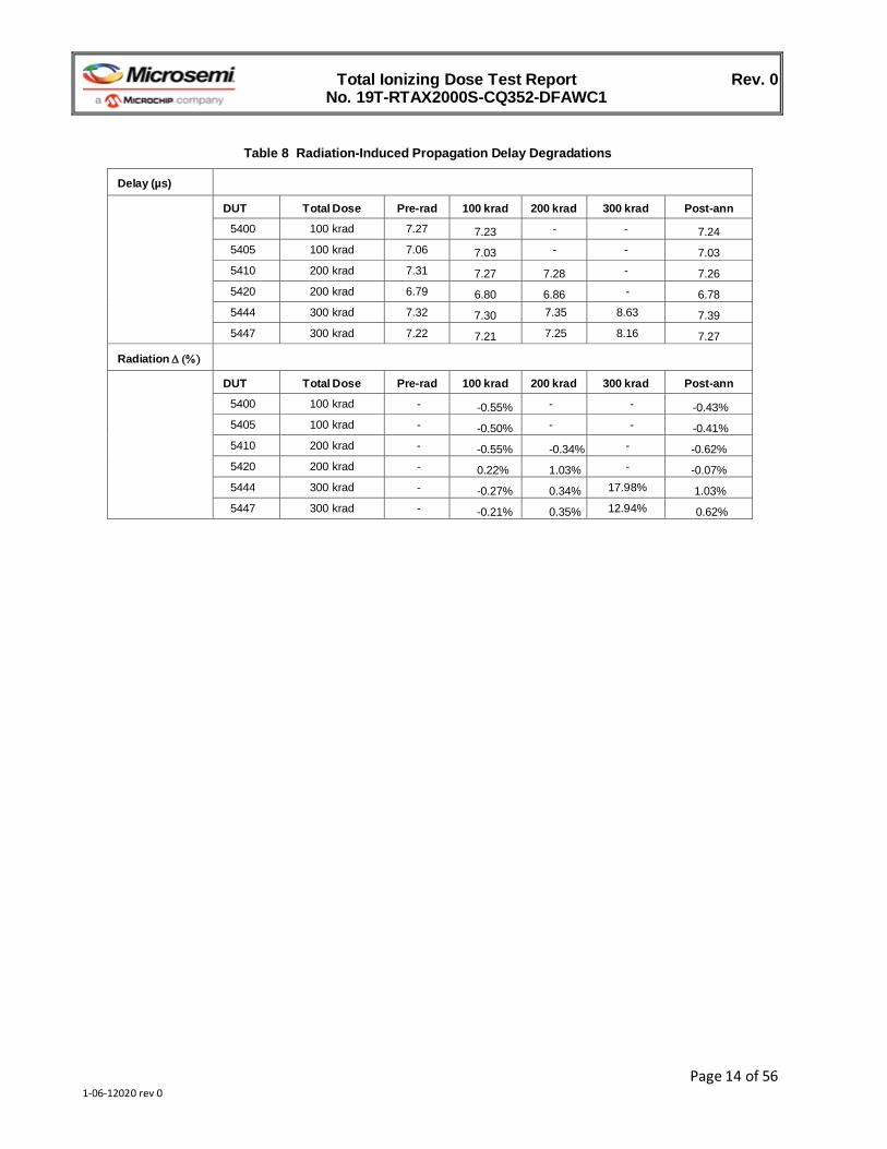
F. Propagation Delay The propagation delay was measured in-situ, post-irradiation, and post-annealing. The results are plotted in Figure 8, and listed in Table 8. As shown in Figure 8, the propagation delay moves with the total dose, but the change is small throughout the irradiation. Referring to influx static current plots (Figure 2 through Figure 7), a device probably heats up as the dose increases. The rising temperature could be the root cause of the increasing trend at high doses. The post-annealing data, on the other hand, show decreased delay in every case.
The radiation delta in every case is well within the 10% degradation criterion. The user can take the worst case for the design margin consideration.
Figure 8 In-Situ Propagation Delay versus Total Dose
6.0
6.5
7.0
7.5
8.0
8.5
9.0
Pre-Irrad 100 krad 200 krad 300 krad Post-Anneal
Del
ay (u
s)
Total Dose
RTAX2000S CQ352 DFAWC1
5444 300krad
5447 300krad
5410 200krad
5420 200krad
5400 100krad
5405 100krad
Total Ionizing Dose Test Report Rev. 0 No. 19T-RTAX2000S-CQ352-DFAWC1
Page 14 of 56 1-06-12020 rev 0
Table 8 Radiation-Induced Propagation Delay Degradations
Delay (µs)
DUT Total Dose Pre-rad 100 krad 200 krad 300 krad Post-ann
5400 100 krad 7.27 7.23 - - 7.24 5405 100 krad 7.06 7.03 - - 7.03 5410 200 krad 7.31 7.27 7.28 - 7.26 5420 200 krad 6.79 6.80 6.86 - 6.78 5444 300 krad 7.32 7.30 7.35 8.63 7.39 5447 300 krad 7.22 7.21 7.25 8.16 7.27
Radiation ∆ (%)
DUT Total Dose Pre-rad 100 krad 200 krad 300 krad Post-ann
5400 100 krad - -0.55% - - -0.43% 5405 100 krad - -0.50% - - -0.41% 5410 200 krad - -0.55% -0.34% - -0.62% 5420 200 krad - 0.22% 1.03% - -0.07% 5444 300 krad - -0.27% 0.34% 17.98% 1.03% 5447 300 krad - -0.21% 0.35% 12.94% 0.62%

Total Ionizing Dose Test Report Rev. 0 No. 19T-RTAX2000S-CQ352-DFAWC1
Page 15 of 56 1-06-12020 rev 0
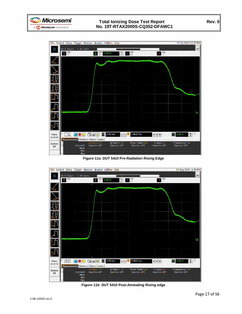
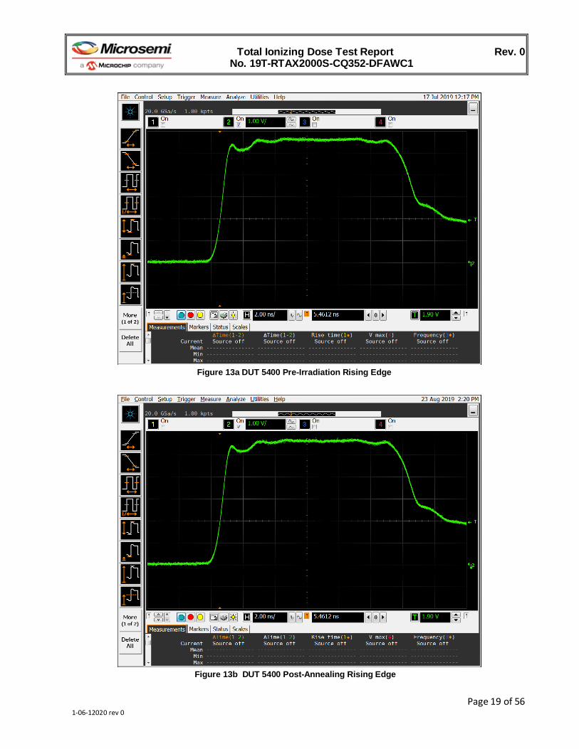
G. Transition Characteristics Figure 9a to Figure 20b show the pre-irradiation and post-annealing transition edges. In each case, the radiation-induced transition-time degradation is insignificant.
Figure 9a DUT 5444 Pre-Irradiation Rising Edge
Figure 9b DUT 5444 Post-Annealing Rising Edge

Total Ionizing Dose Test Report Rev. 0 No. 19T-RTAX2000S-CQ352-DFAWC1
Page 16 of 56 1-06-12020 rev 0
Figure 10a DUT 5447 Pre-Irradiation Rising Edge
Figure 10b DUT 5447 Post-Annealing Rising Edge
Total Ionizing Dose Test Report Rev. 0 No. 19T-RTAX2000S-CQ352-DFAWC1
Page 17 of 56 1-06-12020 rev 0
Figure 11a DUT 5410 Pre-Radiation Rising Edge
Figure 11b DUT 5410 Post-Annealing Rising edge

Total Ionizing Dose Test Report Rev. 0 No. 19T-RTAX2000S-CQ352-DFAWC1
Page 18 of 56 1-06-12020 rev 0
Figure 12a DUT 5420 Pre-Irradiation Rising Edge
Figure 12b DUT 5420 Post-Annealing Rising Edge
Total Ionizing Dose Test Report Rev. 0 No. 19T-RTAX2000S-CQ352-DFAWC1
Page 19 of 56 1-06-12020 rev 0
Figure 13a DUT 5400 Pre-Irradiation Rising Edge
Figure 13b DUT 5400 Post-Annealing Rising Edge

Total Ionizing Dose Test Report Rev. 0 No. 19T-RTAX2000S-CQ352-DFAWC1
Page 20 of 56 1-06-12020 rev 0
Figure 14a DUT 5405 Pre-Irradiation Rising Edge
Figure 14b DUT 5405 Post-Annealing Rising Edge

Total Ionizing Dose Test Report Rev. 0 No. 19T-RTAX2000S-CQ352-DFAWC1
Page 21 of 56 1-06-12020 rev 0
Figure 15a DUT 5444 Pre-Radiation Falling Edge
Figure 15b DUT 5444 Post-Annealing Falling Edge

Total Ionizing Dose Test Report Rev. 0 No. 19T-RTAX2000S-CQ352-DFAWC1
Page 22 of 56 1-06-12020 rev 0
Figure 16a DUT 5447 Pre-Irradiation Falling Edge
Figure 16b DUT 5447 Post-Annealing Falling Edge

Total Ionizing Dose Test Report Rev. 0 No. 19T-RTAX2000S-CQ352-DFAWC1
Page 23 of 56 1-06-12020 rev 0
Figure 17a DUT 5410 Pre-Irradiation Falling Edge
Figure 17b DUT 5410 Post-Annealing Falling Edge

Total Ionizing Dose Test Report Rev. 0 No. 19T-RTAX2000S-CQ352-DFAWC1
Page 24 of 56 1-06-12020 rev 0
Figure 18a DUT 5420 Pre-Irradiation Falling Edge
Figure 18b DUT 5420 Post-Annealing Falling Edge

Total Ionizing Dose Test Report Rev. 0 No. 19T-RTAX2000S-CQ352-DFAWC1
Page 25 of 56 1-06-12020 rev 0
Figure 19a DUT 5400 Pre-Irradiation Falling Edge
Figure 19b DUT 5400 Post-Annealing Falling Edge

Total Ionizing Dose Test Report Rev. 0 No. 19T-RTAX2000S-CQ352-DFAWC1
Page 26 of 56 1-06-12020 rev 0
Figure 20a DUT 5405 Pre-Irradiation Falling Edge
Figure 20b DUT 5405 Post-Annealing Falling Edge

Total Ionizing Dose Test Report Rev. 0 No. 19T-RTAX2000S-CQ352-DFAWC1
Page 27 of 56 1-06-12020 rev 0
Appendix A: DUT Bias
Figure A1 I/O Bias During Irradiation

Total Ionizing Dose Test Report Rev. 0 No. 19T-RTAX2000S-CQ352-DFAWC1
Page 28 of 56 1-06-12020 rev 0
Figure A2 Power Supply, Ground and Special Pins Bias During Irradiation

Total Ionizing Dose Test Report Rev. 0 No. 19T-RTAX2000S-CQ352-DFAWC1
Page 29 of 56 1-06-12020 rev 0
Appendix B: DUT Design Schematics and Verilog Files

Total Ionizing Dose Test Report Rev. 0 No. 19T-RTAX2000S-CQ352-DFAWC1
Page 30 of 56 1-06-12020 rev 0
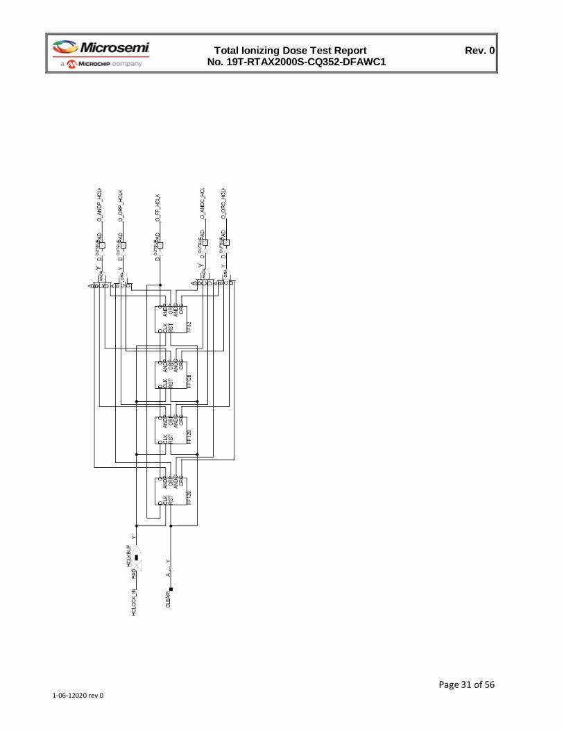
Total Ionizing Dose Test Report Rev. 0 No. 19T-RTAX2000S-CQ352-DFAWC1
Page 31 of 56 1-06-12020 rev 0

Total Ionizing Dose Test Report Rev. 0 No. 19T-RTAX2000S-CQ352-DFAWC1
Page 32 of 56 1-06-12020 rev 0

Total Ionizing Dose Test Report Rev. 0 No. 19T-RTAX2000S-CQ352-DFAWC1
Page 33 of 56 1-06-12020 rev 0

Total Ionizing Dose Test Report Rev. 0 No. 19T-RTAX2000S-CQ352-DFAWC1
Page 34 of 56 1-06-12020 rev 0
Total Ionizing Dose Test Report Rev. 0 No. 19T-RTAX2000S-CQ352-DFAWC1
Page 35 of 56 1-06-12020 rev 0

Total Ionizing Dose Test Report Rev. 0 No. 19T-RTAX2000S-CQ352-DFAWC1
Page 36 of 56 1-06-12020 rev 0
Total Ionizing Dose Test Report Rev. 0 No. 19T-RTAX2000S-CQ352-DFAWC1
Page 37 of 56 1-06-12020 rev 0

Total Ionizing Dose Test Report Rev. 0 No. 19T-RTAX2000S-CQ352-DFAWC1
Page 38 of 56 1-06-12020 rev 0

Total Ionizing Dose Test Report Rev. 0 No. 19T-RTAX2000S-CQ352-DFAWC1
Page 39 of 56 1-06-12020 rev 0

Total Ionizing Dose Test Report Rev. 0 No. 19T-RTAX2000S-CQ352-DFAWC1
Page 40 of 56 1-06-12020 rev 0

Total Ionizing Dose Test Report Rev. 0 No. 19T-RTAX2000S-CQ352-DFAWC1
Page 41 of 56 1-06-12020 rev 0

Total Ionizing Dose Test Report Rev. 0 No. 19T-RTAX2000S-CQ352-DFAWC1
Page 42 of 56 1-06-12020 rev 0

Total Ionizing Dose Test Report Rev. 0 No. 19T-RTAX2000S-CQ352-DFAWC1
Page 43 of 56 1-06-12020 rev 0

Total Ionizing Dose Test Report Rev. 0 No. 19T-RTAX2000S-CQ352-DFAWC1
Page 44 of 56 1-06-12020 rev 0
// BUFF2p3k.v `timescale 1 ns/100 ps
module BUFF2p3k (In, Out);
input In;
output Out;
wire x1/*synthesis syn_keep=1 alspreserve=1*/; wire x2/*synthesis syn_keep=1 alspreserve=1*/; wire x3/*synthesis syn_keep=1 alspreserve=1*/; wire x4/*synthesis syn_keep=1 alspreserve=1*/; wire x5/*synthesis syn_keep=1 alspreserve=1*/; wire x6/*synthesis syn_keep=1 alspreserve=1*/; wire x7/*synthesis syn_keep=1 alspreserve=1*/;
BUFF1k buff1k_1 (.In(In), .Out(x1)); BUFF1k buff1k_2 (.In(x1), .Out(x2)); BUFF50 buff3 (.In(x2), .Out(x3)); BUFF50 buff4 (.In(x3), .Out(x4)); BUFF50 buff5 (.In(x4), .Out(x5)); BUFF50 buff6 (.In(x5), .Out(x6)); BUFF50 buff7 (.In(x6), .Out(x7)); BUFF50 buff8 (.In(x7), .Out(Out));
endmodule
// BUFF1k `timescale 1 ns/100 ps
module BUFF1k (In, Out);
input In;
output Out;
wire x1/*synthesis syn_keep=1 alspreserve=1*/; wire x2/*synthesis syn_keep=1 alspreserve=1*/; wire x3/*synthesis syn_keep=1 alspreserve=1*/; wire x4/*synthesis syn_keep=1 alspreserve=1*/; wire x5/*synthesis syn_keep=1 alspreserve=1*/; wire x6/*synthesis syn_keep=1 alspreserve=1*/; wire x7/*synthesis syn_keep=1 alspreserve=1*/; wire x8/*synthesis syn_keep=1 alspreserve=1*/; wire x9/*synthesis syn_keep=1 alspreserve=1*/; wire x10/*synthesis syn_keep=1 alspreserve=1*/; wire x11/*synthesis syn_keep=1 alspreserve=1*/; wire x12/*synthesis syn_keep=1 alspreserve=1*/; wire x13/*synthesis syn_keep=1 alspreserve=1*/; wire x14/*synthesis syn_keep=1 alspreserve=1*/; wire x15/*synthesis syn_keep=1 alspreserve=1*/; wire x16/*synthesis syn_keep=1 alspreserve=1*/; wire x17/*synthesis syn_keep=1 alspreserve=1*/; wire x18/*synthesis syn_keep=1 alspreserve=1*/; wire x19/*synthesis syn_keep=1 alspreserve=1*/;

Total Ionizing Dose Test Report Rev. 0 No. 19T-RTAX2000S-CQ352-DFAWC1
Page 45 of 56 1-06-12020 rev 0
BUFF50 buff1 (.In(In), .Out(x1)); BUFF50 buff2 (.In(x1), .Out(x2)); BUFF50 buff3 (.In(x2), .Out(x3)); BUFF50 buff4 (.In(x3), .Out(x4)); BUFF50 buff5 (.In(x4), .Out(x5)); BUFF50 buff6 (.In(x5), .Out(x6)); BUFF50 buff7 (.In(x6), .Out(x7)); BUFF50 buff8 (.In(x7), .Out(x8)); BUFF50 buff9 (.In(x8), .Out(x9)); BUFF50 buff10 (.In(x9), .Out(x10));
BUFF50 buff11 (.In(x10), .Out(x11)); BUFF50 buff12 (.In(x11), .Out(x12)); BUFF50 buff13 (.In(x12), .Out(x13)); BUFF50 buff14 (.In(x13), .Out(x14)); BUFF50 buff15 (.In(x14), .Out(x15)); BUFF50 buff16 (.In(x15), .Out(x16)); BUFF50 buff17 (.In(x16), .Out(x17)); BUFF50 buff18 (.In(x17), .Out(x18)); BUFF50 buff19 (.In(x18), .Out(x19)); BUFF50 buff20 (.In(x19), .Out(Out));
endmodule
// BUFF50 `timescale 1 ns/100 ps
module BUFF50 (In, Out);
input In;
output Out;
wire x1 /*synthesis syn_keep=1 alspreserve=1*/; wire x2 /*synthesis syn_keep=1 alspreserve=1*/; wire x3 /*synthesis syn_keep=1 alspreserve=1*/; wire x4 /*synthesis syn_keep=1 alspreserve=1*/; wire x5 /*synthesis syn_keep=1 alspreserve=1*/; wire x6/*synthesis syn_keep=1 alspreserve=1*/; wire x7/*synthesis syn_keep=1 alspreserve=1*/; wire x8/*synthesis syn_keep=1 alspreserve=1*/; wire x9/*synthesis syn_keep=1 alspreserve=1*/; wire x10/*synthesis syn_keep=1 alspreserve=1*/; wire x11/*synthesis syn_keep=1 alspreserve=1*/; wire x12/*synthesis syn_keep=1 alspreserve=1*/; wire x13/*synthesis syn_keep=1 alspreserve=1*/; wire x14/*synthesis syn_keep=1 alspreserve=1*/; wire x15/*synthesis syn_keep=1 alspreserve=1*/; wire x16/*synthesis syn_keep=1 alspreserve=1*/; wire x17/*synthesis syn_keep=1 alspreserve=1*/; wire x18/*synthesis syn_keep=1 alspreserve=1*/; wire x19/*synthesis syn_keep=1 alspreserve=1*/; wire x20/*synthesis syn_keep=1 alspreserve=1*/; wire x21/*synthesis syn_keep=1 alspreserve=1*/; wire x22/*synthesis syn_keep=1 alspreserve=1*/;

Total Ionizing Dose Test Report Rev. 0 No. 19T-RTAX2000S-CQ352-DFAWC1
Page 46 of 56 1-06-12020 rev 0
wire x23/*synthesis syn_keep=1 alspreserve=1*/; wire x24/*synthesis syn_keep=1 alspreserve=1*/; wire x25/*synthesis syn_keep=1 alspreserve=1*/; wire x26/*synthesis syn_keep=1 alspreserve=1*/; wire x27/*synthesis syn_keep=1 alspreserve=1*/; wire x28/*synthesis syn_keep=1 alspreserve=1*/; wire x29/*synthesis syn_keep=1 alspreserve=1*/; wire x30/*synthesis syn_keep=1 alspreserve=1*/; wire x31/*synthesis syn_keep=1 alspreserve=1*/; wire x32/*synthesis syn_keep=1 alspreserve=1*/; wire x33/*synthesis syn_keep=1 alspreserve=1*/; wire x34/*synthesis syn_keep=1 alspreserve=1*/; wire x35/*synthesis syn_keep=1 alspreserve=1*/; wire x36/*synthesis syn_keep=1 alspreserve=1*/; wire x37/*synthesis syn_keep=1 alspreserve=1*/; wire x38/*synthesis syn_keep=1 alspreserve=1*/; wire x39/*synthesis syn_keep=1 alspreserve=1*/; wire x40/*synthesis syn_keep=1 alspreserve=1*/; wire x41/*synthesis syn_keep=1 alspreserve=1*/; wire x42/*synthesis syn_keep=1 alspreserve=1*/; wire x43/*synthesis syn_keep=1 alspreserve=1*/; wire x44/*synthesis syn_keep=1 alspreserve=1*/; wire x45/*synthesis syn_keep=1 alspreserve=1*/; wire x46/*synthesis syn_keep=1 alspreserve=1*/; wire x47/*synthesis syn_keep=1 alspreserve=1*/; wire x48/*synthesis syn_keep=1 alspreserve=1*/; wire x49/*synthesis syn_keep=1 alspreserve=1*/;
BUFF buff1 (.A(In), .Y(x1)); BUFF buff2 (.A(x1), .Y(x2)); BUFF buff3 (.A(x2), .Y(x3)); BUFF buff4 (.A(x3), .Y(x4)); BUFF buff5 (.A(x4), .Y(x5)); BUFF buff6 (.A(x5), .Y(x6)); BUFF buff7 (.A(x6), .Y(x7)); BUFF buff8 (.A(x7), .Y(x8)); BUFF buff9 (.A(x8), .Y(x9)); BUFF buff10 (.A(x9), .Y(x10));
BUFF buff11 (.A(x10), .Y(x11)); BUFF buff12 (.A(x11), .Y(x12)); BUFF buff13 (.A(x12), .Y(x13)); BUFF buff14 (.A(x13), .Y(x14)); BUFF buff15 (.A(x14), .Y(x15)); BUFF buff16 (.A(x15), .Y(x16)); BUFF buff17 (.A(x16), .Y(x17)); BUFF buff18 (.A(x17), .Y(x18)); BUFF buff19 (.A(x18), .Y(x19)); BUFF buff20 (.A(x19), .Y(x20));
BUFF buff21 (.A(x20), .Y(x21)); BUFF buff22 (.A(x21), .Y(x22)); BUFF buff23 (.A(x22), .Y(x23)); BUFF buff24 (.A(x23), .Y(x24)); BUFF buff25 (.A(x24), .Y(x25)); BUFF buff26 (.A(x25), .Y(x26));

Total Ionizing Dose Test Report Rev. 0 No. 19T-RTAX2000S-CQ352-DFAWC1
Page 47 of 56 1-06-12020 rev 0
BUFF buff27 (.A(x26), .Y(x27)); BUFF buff28 (.A(x27), .Y(x28)); BUFF buff29 (.A(x28), .Y(x29)); BUFF buff30 (.A(x29), .Y(x30));
BUFF buff31 (.A(x30), .Y(x31)); BUFF buff32 (.A(x31), .Y(x32)); BUFF buff33 (.A(x32), .Y(x33)); BUFF buff34 (.A(x33), .Y(x34)); BUFF buff35 (.A(x34), .Y(x35)); BUFF buff36 (.A(x35), .Y(x36)); BUFF buff37 (.A(x36), .Y(x37)); BUFF buff38 (.A(x37), .Y(x38)); BUFF buff39 (.A(x38), .Y(x39)); BUFF buff40 (.A(x39), .Y(x40));
BUFF buff41 (.A(x40), .Y(x41)); BUFF buff42 (.A(x41), .Y(x42)); BUFF buff43 (.A(x42), .Y(x43)); BUFF buff44 (.A(x43), .Y(x44)); BUFF buff45 (.A(x44), .Y(x45)); BUFF buff46 (.A(x45), .Y(x46)); BUFF buff47 (.A(x46), .Y(x47)); BUFF buff48 (.A(x47), .Y(x48)); BUFF buff49 (.A(x48), .Y(x49)); BUFF buff50 (.A(x49), .Y(Out));
endmodule
// FF128 `timescale 1 ns/100 ps module FF128 (D, Q, CLK, RST, ANDP, ORP, ANDC, ORC);
input D, CLK, RST; output Q, ANDP, ORP, ANDC, ORC;
wire x1, x2, x3, Q; wire andp_a, andp_b, andp_c, andp_d, orp_a, orp_b, orp_c, orp_d; wire andc_a, andc_b, andc_c, andc_d, orc_a, orc_b, orc_c, orc_d;
FF32 dff_a (.D(D), .Q(x1), .CLK(CLK), .RST(RST), .ANDP(andp_a), .ORP(orp_a), .ANDC(andc_a), .ORC(orc_a));
FF32 dff_b (.D(x1), .Q(x2), .CLK(CLK), .RST(RST), .ANDP(andp_b), .ORP(orp_b), .ANDC(andc_b), .ORC(orc_b));
FF32 dff_c (.D(x2), .Q(x3), .CLK(CLK), .RST(RST), .ANDP(andp_c), .ORP(orp_c), .ANDC(andc_c), .ORC(orc_c));
FF32 dff_d (.D(x3), .Q(Q), .CLK(CLK), .RST(RST), .ANDP(andp_d), .ORP(orp_d), .ANDC(andc_d), .ORC(orc_d));
AND4 and4p (.A(andp_a), .B(andp_b), .C(andp_c), .D(andp_d), .Y(ANDP)); OR4 or4p (.A(orp_a), .B(orp_b), .C(orp_c), .D(orp_d), .Y(ORP));
AND4 and4c (.A(andc_a), .B(andc_b), .C(andc_c), .D(andc_d), .Y(ANDC));

Total Ionizing Dose Test Report Rev. 0 No. 19T-RTAX2000S-CQ352-DFAWC1
Page 48 of 56 1-06-12020 rev 0
OR4 or4c (.A(orc_a), .B(orc_b), .C(orc_c), .D(orc_d), .Y(ORC));
endmodule
// FF32 `timescale 1 ns/100 ps module FF32 (D, Q, CLK, RST, ANDP, ORP, ANDC, ORC);
input D, CLK, RST; output Q, ANDP, ORP, ANDC, ORC;
wire x1, x2, x3, Q; wire andp_a, andp_b, andp_c, andp_d, orp_a, orp_b, orp_c, orp_d; wire andc_a, andc_b, andc_c, andc_d, orc_a, orc_b, orc_c, orc_d;
FF8 dff_a (.D(D), .Q(x1), .CLK(CLK), .RST(RST), .ANDP(andp_a), .ORP(orp_a), .ANDC(andc_a), .ORC(orc_a));
FF8 dff_b (.D(x1), .Q(x2), .CLK(CLK), .RST(RST), .ANDP(andp_b), .ORP(orp_b), .ANDC(andc_b), .ORC(orc_b));
FF8 dff_c (.D(x2), .Q(x3), .CLK(CLK), .RST(RST), .ANDP(andp_c), .ORP(orp_c), .ANDC(andc_c), .ORC(orc_c));
FF8 dff_d (.D(x3), .Q(Q), .CLK(CLK), .RST(RST), .ANDP(andp_d), .ORP(orp_d), .ANDC(andc_d), .ORC(orc_d));
AND4 and4p (.A(andp_a), .B(andp_b), .C(andp_c), .D(andp_d), .Y(ANDP)); OR4 or4p (.A(orp_a), .B(orp_b), .C(orp_c), .D(orp_d), .Y(ORP));
AND4 and4c (.A(andc_a), .B(andc_b), .C(andc_c), .D(andc_d), .Y(ANDC)); OR4 or4c (.A(orc_a), .B(orc_b), .C(orc_c), .D(orc_d), .Y(ORC));
endmodule
// FF8 `timescale 1 ns/100 ps
module FF8 (D, Q, CLK, RST, ANDP, ORP, ANDC, ORC);
input D, CLK, RST; output Q, ANDP, ORP, ANDC, ORC;
wire x1, x2, x3, x4, x5, x6, x7;
DFC1B dff1 (.D(D), .Q(x1), .CLK(CLK), .CLR(RST)); DFP1B dff2 (.D(x1), .Q(x2), .CLK(CLK), .PRE(RST)); DFC1B dff3 (.D(x2), .Q(x3), .CLK(CLK), .CLR(RST)); DFP1B dff4 (.D(x3), .Q(x4), .CLK(CLK), .PRE(RST)); DFC1B dff5 (.D(x4), .Q(x5), .CLK(CLK), .CLR(RST)); DFP1B dff6 (.D(x5), .Q(x6), .CLK(CLK), .PRE(RST)); DFC1B dff7 (.D(x6), .Q(x7), .CLK(CLK), .CLR(RST)); DFP1B dff8 (.D(x7), .Q(Q), .CLK(CLK), .PRE(RST));
AND4 and4p (.A(x2), .B(x4), .C(x6), .D(Q), .Y(ANDP)); OR4 or4p (.A(x2), .B(x4), .C(x6), .D(Q), .Y(ORP));

Total Ionizing Dose Test Report Rev. 0 No. 19T-RTAX2000S-CQ352-DFAWC1
Page 49 of 56 1-06-12020 rev 0
AND4 and4c (.A(x1), .B(x3), .C(x5), .D(x7), .Y(ANDC)); OR4 or4c (.A(x1), .B(x3), .C(x5), .D(x7), .Y(ORC));
endmodule
// Top_RAM_Module.v `timescale 1 ns/100 ps
module Top_RAM_Module(Psel0, Psel1, RC_en, RC_clr, RC_clk, Write, Read, Wclk, Rclk,
Q_RAM); input Psel0, Psel1, RC_en, RC_clr, RC_clk, Write, Read, Wclk, Rclk; output [5:0] Q_RAM;
wire Gnd, Vcc; wire mx0, mx1; wire [12:0] rc; wire [3:0] dec; wire y_0w, y_0r, y_1w, y_1r, y_2w, y_2r, y_3w, y_3r; // y_4w, y_4r, y_5w, y_5r, y_6w, y_6r, y_7w, y_7r; wire [5:0] DIN; wire [5:0] Q_b0; wire [5:0] Q_b1; wire [5:0] Q_b2; wire [5:0] Q_b3; //wire [5:0] Q_b4; //wire [5:0] Q_b5; //wire [5:0] Q_b6; //wire [5:0] Q_b7;
GND gnd_0(.Y(Gnd)); VCC vcc_0(.Y(Vcc));
mux_2x1 mux_0(.Data0_port(Gnd), .Data1_port(Vcc), .Sel0(Psel0), .Result(mx0)); mux_2x1 mux_1(.Data0_port(Gnd), .Data1_port(Vcc), .Sel0(Psel1), .Result(mx1));
counter_13 counter_0(.Enable(RC_en), .Aclr(RC_clr), .Clock(RC_clk), .Q(rc));
decoder_2to4 decoder_0(.Data0(rc[11]), .Data1(rc[12]), .Eq(dec));
NAND2 nand_0w(.A(dec[0]), .B(Write), .Y(y_0w)); NAND2 nand_0r(.A(dec[0]), .B(Read), .Y(y_0r));
ram_2048x6 ram_blk0(.Data(DIN), .Q(Q_b0), .WAddress(rc[10:0]), .RAddress(rc[10:0]),
.WE(y_0w), .RE(y_0r), .WClock(Wclk), .RClock(Rclk));
assign DIN[0]=mx0, DIN[1]=mx1, DIN[2]=mx0, DIN[3]=mx1, DIN[4]=mx0, DIN[5]=mx1;
NAND2 nand_1w(.A(dec[1]), .B(Write), .Y(y_1w)); NAND2 nand_1r(.A(dec[1]), .B(Read), .Y(y_1r));
ram_2048x6 ram_blk1(.Data(DIN), .Q(Q_b1), .WAddress(rc[10:0]), .RAddress(rc[10:0]),
.WE(y_1w), .RE(y_1r), .WClock(Wclk), .RClock(Rclk));
NAND2 nand_2w(.A(dec[2]), .B(Write), .Y(y_2w)); NAND2 nand_2r(.A(dec[2]), .B(Read), .Y(y_2r));

Total Ionizing Dose Test Report Rev. 0 No. 19T-RTAX2000S-CQ352-DFAWC1
Page 50 of 56 1-06-12020 rev 0
ram_2048x6 ram_blk2(.Data(DIN), .Q(Q_b2), .WAddress(rc[10:0]), .RAddress(rc[10:0]), .WE(y_2w), .RE(y_2r), .WClock(Wclk), .RClock(Rclk));
NAND2 nand_3w(.A(dec[3]), .B(Write), .Y(y_3w)); NAND2 nand_3r(.A(dec[3]), .B(Read), .Y(y_3r));
ram_2048x6 ram_blk3(.Data(DIN),
.Q(Q_b3), .WAddress(rc[10:0]), .RAddress(rc[10:0]),
.WE(y_3w), .RE(y_3r), .WClock(Wclk), .RClock(Rclk));
/* NAND2 nand_4w(.A(dec[4]), .B(Write), .Y(y_4w)); NAND2 nand_4r(.A(dec[4]), .B(Read), .Y(y_4r));
ram_2048x3 ram_blk4(.Data(DIN),
.Q(Q_b4), .WAddress(rc[10:0]), .RAddress(rc[10:0]),
.WE(y_4w), .RE(y_4r), .WClock(Wclk), .RClock(Rclk));
NAND2 nand_5w(.A(dec[5]), .B(Write), .Y(y_5w)); NAND2 nand_5r(.A(dec[5]), .B(Read), .Y(y_5r));
ram_2048x3 ram_blk5(.Data(DIN),
.Q(Q_b5), .WAddress(rc[10:0]), .RAddress(rc[10:0]),
.WE(y_5w), .RE(y_5r), .WClock(Wclk), .RClock(Rclk));
NAND2 nand_6w(.A(dec[6]), .B(Write), .Y(y_6w)); NAND2 nand_6r(.A(dec[6]), .B(Read), .Y(y_6r));
ram_2048x3 ram_blk6(.Data(DIN),
.Q(Q_b6), .WAddress(rc[10:0]), .RAddress(rc[10:0]),
.WE(y_6w), .RE(y_6r), .WClock(Wclk), .RClock(Rclk));
NAND2 nand_7w(.A(dec[7]), .B(Write), .Y(y_7w)); NAND2 nand_7r(.A(dec[7]), .B(Read), .Y(y_7r));
ram_2048x3 ram_blk7(.Data(DIN),
.Q(Q_b7), .WAddress(rc[10:0]), .RAddress(rc[10:0]),
.WE(y_7w), .RE(y_7r), .WClock(Wclk), .RClock(Rclk)); */
mux_6x4 mux_6x4_0(.Data0_port(Q_b0), .Data1_port(Q_b1), .Data2_port(Q_b2), .Data3_port(Q_b3), .Sel0(rc[11]), .Sel1(rc[12]), .Result(Q_RAM));
endmodule

Total Ionizing Dose Test Report Rev. 0 No. 19T-RTAX2000S-CQ352-DFAWC1
Page 51 of 56 1-06-12020 rev 0
`timescale 1 ns/100 ps // Version: 6.0 SP3 6.0.30.3
module mux_2x1(Data0_port,Data1_port,Sel0,Result); input Data0_port, Data1_port, Sel0; output Result;
MX2 MX2_Result(.A(Data0_port), .B(Data1_port), .S(Sel0), .Y( Result));
endmodule
`timescale 1 ns/100 ps // Version: 6.2 SP2 6.2.52.7
module counter_13(Enable,Aclr,Clock,Q); input Enable, Aclr, Clock; output [12:0] Q;
wire ClrAux_0_net, ClrAux_7_net, MX2_1_Y, MX2_7_Y, MX2_4_Y,
CM8_0_Y, MX2_10_Y, MX2_9_Y, MX2_3_Y, MX2_5_Y, MX2_6_Y, MX2_0_Y, MX2_8_Y, MX2_2_Y, MX2_11_Y, VCC, GND;
VCC VCC_1_net(.Y(VCC)); GND GND_1_net(.Y(GND)); DFC1D DFC1D_Q_7_inst(.D(MX2_1_Y), .CLK(Q[6]), .CLR(
ClrAux_7_net), .Q(Q[7])); DFC1D DFC1D_Q_1_inst(.D(MX2_7_Y), .CLK(Q[0]), .CLR(
ClrAux_0_net), .Q(Q[1])); BUFF BUFF_ClrAux_0_inst(.A(Aclr), .Y(ClrAux_0_net)); MX2 MX2_9(.A(VCC), .B(GND), .S(Q[5]), .Y(MX2_9_Y)); DFC1D DFC1D_Q_2_inst(.D(MX2_6_Y), .CLK(Q[1]), .CLR(
ClrAux_0_net), .Q(Q[2])); MX2 MX2_0(.A(VCC), .B(GND), .S(Q[8]), .Y(MX2_0_Y)); DFC1D DFC1D_Q_12_inst(.D(MX2_4_Y), .CLK(Q[11]), .CLR(
ClrAux_7_net), .Q(Q[12])); DFC1D DFC1D_Q_3_inst(.D(MX2_11_Y), .CLK(Q[2]), .CLR(
ClrAux_0_net), .Q(Q[3])); DFC1D DFC1D_Q_4_inst(.D(MX2_5_Y), .CLK(Q[3]), .CLR(
ClrAux_0_net), .Q(Q[4])); CM8 CM8_0(.D0(GND), .D1(VCC), .D2(VCC), .D3(GND), .S00(Q[0]),
.S01(VCC), .S10(Enable), .S11(GND), .Y(CM8_0_Y)); MX2 MX2_11(.A(VCC), .B(GND), .S(Q[3]), .Y(MX2_11_Y)); DFC1B DFC1B_Q_0_inst(.D(CM8_0_Y), .CLK(Clock), .CLR(
ClrAux_0_net), .Q(Q[0])); MX2 MX2_6(.A(VCC), .B(GND), .S(Q[2]), .Y(MX2_6_Y)); MX2 MX2_3(.A(VCC), .B(GND), .S(Q[10]), .Y(MX2_3_Y)); DFC1D DFC1D_Q_11_inst(.D(MX2_10_Y), .CLK(Q[10]), .CLR(
ClrAux_7_net), .Q(Q[11])); MX2 MX2_10(.A(VCC), .B(GND), .S(Q[11]), .Y(MX2_10_Y)); BUFF BUFF_ClrAux_7_inst(.A(Aclr), .Y(ClrAux_7_net)); MX2 MX2_4(.A(VCC), .B(GND), .S(Q[12]), .Y(MX2_4_Y)); DFC1D DFC1D_Q_5_inst(.D(MX2_9_Y), .CLK(Q[4]), .CLR(
Total Ionizing Dose Test Report Rev. 0 No. 19T-RTAX2000S-CQ352-DFAWC1
Page 52 of 56 1-06-12020 rev 0
ClrAux_0_net), .Q(Q[5])); DFC1D DFC1D_Q_9_inst(.D(MX2_8_Y), .CLK(Q[8]), .CLR(
ClrAux_7_net), .Q(Q[9])); MX2 MX2_5(.A(VCC), .B(GND), .S(Q[4]), .Y(MX2_5_Y)); MX2 MX2_8(.A(VCC), .B(GND), .S(Q[9]), .Y(MX2_8_Y)); DFC1D DFC1D_Q_8_inst(.D(MX2_0_Y), .CLK(Q[7]), .CLR(
ClrAux_7_net), .Q(Q[8])); MX2 MX2_2(.A(VCC), .B(GND), .S(Q[6]), .Y(MX2_2_Y)); MX2 MX2_7(.A(VCC), .B(GND), .S(Q[1]), .Y(MX2_7_Y)); MX2 MX2_1(.A(VCC), .B(GND), .S(Q[7]), .Y(MX2_1_Y)); DFC1D DFC1D_Q_6_inst(.D(MX2_2_Y), .CLK(Q[5]), .CLR(
ClrAux_0_net), .Q(Q[6])); DFC1D DFC1D_Q_10_inst(.D(MX2_3_Y), .CLK(Q[9]), .CLR(
ClrAux_7_net), .Q(Q[10]));
endmodule
`timescale 1 ns/100 ps // Version: 6.2 SP2 6.2.52.7
module decoder_2to4(Data0,Data1,Eq); input Data0, Data1; output [3:0] Eq;
AND2A AND2A_Eq_1_inst(.A(Data1), .B(Data0), .Y(Eq[1])); AND2 AND2_Eq_3_inst(.A(Data0), .B(Data1), .Y(Eq[3])); AND2A AND2A_Eq_2_inst(.A(Data0), .B(Data1), .Y(Eq[2])); AND2B AND2B_Eq_0_inst(.A(Data0), .B(Data1), .Y(Eq[0]));
endmodule
`timescale 1 ns/100 ps // Version: 6.2 SP2 6.2.52.7
module ram_2048x6(Data,Q,WAddress,RAddress,WE,RE,WClock,RClock); input [5:0] Data; output [5:0] Q; input [10:0] WAddress, RAddress; input WE, RE, WClock, RClock;
wire WEP, REP, VCC, GND;
VCC VCC_1_net(.Y(VCC)); GND GND_1_net(.Y(GND)); RAM64K36P ram_2048x6_R0C2(.WCLK(WClock), .RCLK(RClock),
.DEPTH0(GND), .DEPTH1(GND), .DEPTH2(GND), .DEPTH3(GND),
.WEN(WEP), .WW0(VCC), .WW1(GND), .WW2(GND), .WRAD0( WAddress[0]), .WRAD1(WAddress[1]), .WRAD2(WAddress[2]), .WRAD3(WAddress[3]), .WRAD4(WAddress[4]), .WRAD5( WAddress[5]), .WRAD6(WAddress[6]), .WRAD7(WAddress[7]), .WRAD8(WAddress[8]), .WRAD9(WAddress[9]), .WRAD10( WAddress[10]), .WRAD11(GND), .WRAD12(GND), .WRAD13(GND), .WRAD14(GND), .WRAD15(GND), .WD0(Data[4]), .WD1(Data[5]),

Total Ionizing Dose Test Report Rev. 0 No. 19T-RTAX2000S-CQ352-DFAWC1
Page 53 of 56 1-06-12020 rev 0
.WD2(GND), .WD3(GND), .WD4(GND), .WD5(GND), .WD6(GND),
.WD7(GND), .WD8(GND), .WD9(GND), .WD10(GND), .WD11(GND),
.WD12(GND), .WD13(GND), .WD14(GND), .WD15(GND), .WD16(GND) , .WD17(GND), .WD18(GND), .WD19(GND), .WD20(GND), .WD21( GND), .WD22(GND), .WD23(GND), .WD24(GND), .WD25(GND), .WD26(GND), .WD27(GND), .WD28(GND), .WD29(GND), .WD30(GND) , .WD31(GND), .WD32(GND), .WD33(GND), .WD34(GND), .WD35( GND), .REN(REP), .RW0(VCC), .RW1(GND), .RW2(GND), .RDAD0( RAddress[0]), .RDAD1(RAddress[1]), .RDAD2(RAddress[2]), .RDAD3(RAddress[3]), .RDAD4(RAddress[4]), .RDAD5( RAddress[5]), .RDAD6(RAddress[6]), .RDAD7(RAddress[7]), .RDAD8(RAddress[8]), .RDAD9(RAddress[9]), .RDAD10( RAddress[10]), .RDAD11(GND), .RDAD12(GND), .RDAD13(GND), .RDAD14(GND), .RDAD15(GND), .RD0(Q[4]), .RD1(Q[5]), .RD2() , .RD3(), .RD4(), .RD5(), .RD6(), .RD7(), .RD8(), .RD9(), .RD10(), .RD11(), .RD12(), .RD13(), .RD14(), .RD15(), .RD16(), .RD17(), .RD18(), .RD19(), .RD20(), .RD21(), .RD22(), .RD23(), .RD24(), .RD25(), .RD26(), .RD27(), .RD28(), .RD29(), .RD30(), .RD31(), .RD32(), .RD33(), .RD34(), .RD35());
INV REBUBBLE(.A(RE), .Y(REP)); INV WEBUBBLE(.A(WE), .Y(WEP)); RAM64K36P ram_2048x6_R0C1(.WCLK(WClock), .RCLK(RClock),
.DEPTH0(GND), .DEPTH1(GND), .DEPTH2(GND), .DEPTH3(GND),
.WEN(WEP), .WW0(VCC), .WW1(GND), .WW2(GND), .WRAD0( WAddress[0]), .WRAD1(WAddress[1]), .WRAD2(WAddress[2]), .WRAD3(WAddress[3]), .WRAD4(WAddress[4]), .WRAD5( WAddress[5]), .WRAD6(WAddress[6]), .WRAD7(WAddress[7]), .WRAD8(WAddress[8]), .WRAD9(WAddress[9]), .WRAD10( WAddress[10]), .WRAD11(GND), .WRAD12(GND), .WRAD13(GND), .WRAD14(GND), .WRAD15(GND), .WD0(Data[2]), .WD1(Data[3]), .WD2(GND), .WD3(GND), .WD4(GND), .WD5(GND), .WD6(GND), .WD7(GND), .WD8(GND), .WD9(GND), .WD10(GND), .WD11(GND), .WD12(GND), .WD13(GND), .WD14(GND), .WD15(GND), .WD16(GND) , .WD17(GND), .WD18(GND), .WD19(GND), .WD20(GND), .WD21( GND), .WD22(GND), .WD23(GND), .WD24(GND), .WD25(GND), .WD26(GND), .WD27(GND), .WD28(GND), .WD29(GND), .WD30(GND) , .WD31(GND), .WD32(GND), .WD33(GND), .WD34(GND), .WD35( GND), .REN(REP), .RW0(VCC), .RW1(GND), .RW2(GND), .RDAD0( RAddress[0]), .RDAD1(RAddress[1]), .RDAD2(RAddress[2]), .RDAD3(RAddress[3]), .RDAD4(RAddress[4]), .RDAD5( RAddress[5]), .RDAD6(RAddress[6]), .RDAD7(RAddress[7]), .RDAD8(RAddress[8]), .RDAD9(RAddress[9]), .RDAD10( RAddress[10]), .RDAD11(GND), .RDAD12(GND), .RDAD13(GND), .RDAD14(GND), .RDAD15(GND), .RD0(Q[2]), .RD1(Q[3]), .RD2() , .RD3(), .RD4(), .RD5(), .RD6(), .RD7(), .RD8(), .RD9(), .RD10(), .RD11(), .RD12(), .RD13(), .RD14(), .RD15(), .RD16(), .RD17(), .RD18(), .RD19(), .RD20(), .RD21(), .RD22(), .RD23(), .RD24(), .RD25(), .RD26(), .RD27(), .RD28(), .RD29(), .RD30(), .RD31(), .RD32(), .RD33(), .RD34(), .RD35());
RAM64K36P ram_2048x6_R0C0(.WCLK(WClock), .RCLK(RClock), .DEPTH0(GND), .DEPTH1(GND), .DEPTH2(GND), .DEPTH3(GND), .WEN(WEP), .WW0(VCC), .WW1(GND), .WW2(GND), .WRAD0( WAddress[0]), .WRAD1(WAddress[1]), .WRAD2(WAddress[2]), .WRAD3(WAddress[3]), .WRAD4(WAddress[4]), .WRAD5(

Total Ionizing Dose Test Report Rev. 0 No. 19T-RTAX2000S-CQ352-DFAWC1
Page 54 of 56 1-06-12020 rev 0
WAddress[5]), .WRAD6(WAddress[6]), .WRAD7(WAddress[7]), .WRAD8(WAddress[8]), .WRAD9(WAddress[9]), .WRAD10( WAddress[10]), .WRAD11(GND), .WRAD12(GND), .WRAD13(GND), .WRAD14(GND), .WRAD15(GND), .WD0(Data[0]), .WD1(Data[1]), .WD2(GND), .WD3(GND), .WD4(GND), .WD5(GND), .WD6(GND), .WD7(GND), .WD8(GND), .WD9(GND), .WD10(GND), .WD11(GND), .WD12(GND), .WD13(GND), .WD14(GND), .WD15(GND), .WD16(GND) , .WD17(GND), .WD18(GND), .WD19(GND), .WD20(GND), .WD21( GND), .WD22(GND), .WD23(GND), .WD24(GND), .WD25(GND), .WD26(GND), .WD27(GND), .WD28(GND), .WD29(GND), .WD30(GND) , .WD31(GND), .WD32(GND), .WD33(GND), .WD34(GND), .WD35( GND), .REN(REP), .RW0(VCC), .RW1(GND), .RW2(GND), .RDAD0( RAddress[0]), .RDAD1(RAddress[1]), .RDAD2(RAddress[2]), .RDAD3(RAddress[3]), .RDAD4(RAddress[4]), .RDAD5( RAddress[5]), .RDAD6(RAddress[6]), .RDAD7(RAddress[7]), .RDAD8(RAddress[8]), .RDAD9(RAddress[9]), .RDAD10( RAddress[10]), .RDAD11(GND), .RDAD12(GND), .RDAD13(GND), .RDAD14(GND), .RDAD15(GND), .RD0(Q[0]), .RD1(Q[1]), .RD2() , .RD3(), .RD4(), .RD5(), .RD6(), .RD7(), .RD8(), .RD9(), .RD10(), .RD11(), .RD12(), .RD13(), .RD14(), .RD15(), .RD16(), .RD17(), .RD18(), .RD19(), .RD20(), .RD21(), .RD22(), .RD23(), .RD24(), .RD25(), .RD26(), .RD27(), .RD28(), .RD29(), .RD30(), .RD31(), .RD32(), .RD33(), .RD34(), .RD35());
endmodule
`timescale 1 ns/100 ps // Version: 6.2 SP2 6.2.52.7
module mux_6x4(Data0_port,Data1_port,Data2_port,Data3_port,Sel0,
Sel1,Result); input [5:0] Data0_port, Data1_port, Data2_port, Data3_port; input Sel0, Sel1; output [5:0] Result;
MX4 MX4_Result_0_inst(.D0(Data0_port[0]), .D1(Data1_port[0]),
.D2(Data2_port[0]), .D3(Data3_port[0]), .S0(Sel0), .S1( Sel1), .Y(Result[0]));
MX4 MX4_Result_2_inst(.D0(Data0_port[2]), .D1(Data1_port[2]), .D2(Data2_port[2]), .D3(Data3_port[2]), .S0(Sel0), .S1( Sel1), .Y(Result[2]));
MX4 MX4_Result_5_inst(.D0(Data0_port[5]), .D1(Data1_port[5]), .D2(Data2_port[5]), .D3(Data3_port[5]), .S0(Sel0), .S1( Sel1), .Y(Result[5]));
MX4 MX4_Result_1_inst(.D0(Data0_port[1]), .D1(Data1_port[1]), .D2(Data2_port[1]), .D3(Data3_port[1]), .S0(Sel0), .S1( Sel1), .Y(Result[1]));
MX4 MX4_Result_4_inst(.D0(Data0_port[4]), .D1(Data1_port[4]), .D2(Data2_port[4]), .D3(Data3_port[4]), .S0(Sel0), .S1( Sel1), .Y(Result[4]));
MX4 MX4_Result_3_inst(.D0(Data0_port[3]), .D1(Data1_port[3]), .D2(Data2_port[3]), .D3(Data3_port[3]), .S0(Sel0), .S1( Sel1), .Y(Result[3]));
endmodule
Total Ionizing Dose Test Report Rev. 0 No. 19T-RTAX2000S-CQ352-DFAWC1
Page 55 of 56 1-06-12020 rev 0

© 2015–2018 Microsemi. All rights reserved. Microsemi and the Microsemi logo are trademarks of Microsemi Corporation. All other trademarks and service marks are the property of their respective owners.
Microsemi makes no warranty, representation, or guarantee regarding the information contained herein or the suitability of its products and services for any particular purpose, nor does Microsemi assume any liability whatsoever arising out of the application or use of any product or circuit. The products sold hereunder and any other products sold by Microsemi have been subject to limited testing and should not be used in conjunction with mission-critical equipment or applications. Any performance specifications are believed to be reliable but are not verified, and Buyer must conduct and complete all performance and other testing of the products, alone and together with, or installed in, any end-products. Buyer shall not rely on any data and performance specifications or parameters provided by Microsemi. It is the Buyer’s responsibility to independently determine suitability of any products and to test and verify the same. The information provided by Microsemi hereunder is provided “as is, where is” and with all faults, and the entire risk associated with such information is entirely with the Buyer. Microsemi does not grant, explicitly or implicitly, to any party any patent rights, licenses, or any other IP rights, whether with regard to such information itself or anything described by such information. Information provided in this document is proprietary to Microsemi, and Microsemi reserves the right to make any changes to the information in this document or to any products and services at any time without notice. Microsemi, a wholly owned subsidiary of Microchip Technology Inc. (Nasdaq: MCHP), offers a comprehensive portfolio of semiconductor and system solutions for aerospace & defense, communications, data center and industrial markets. Products include high-performance and radiation-hardened analog mixed-signal integrated circuits, FPGAs, SoCs and ASICs; power management products; timing and synchronization devices and precise time solutions, setting the world's standard for time; voice processing devices; RF solutions; discrete components; enterprise storage and communication solutions; security technologies and scalable anti-tamper products; Ethernet solutions; Power-over-Ethernet ICs and midspans; as well as custom design capabilities and services. Microsemi is headquartered in Aliso Viejo, California, and has approximately 4,800 employees globally. Learn more at www. microsemi.com.
Microsemi Headquarters One Enterprise, Aliso Viejo, CA 92656 USA Within the USA: +1 (800) 713-4113 Outside the USA: +1 (949) 380-6100 Sales: +1 (949) 380-6136 Fax: +1 (949) 215-4996 Email: [email protected] www.microsemi.com