tms320f2810, tms320f2811, tms320f2812 ... - mcu & dsp
TRANSCRIPT
TMS320F2810, TMS320F2811, TMS320F2812TMS320C2810, TMS320C2811, TMS320C2812
Digital Signal Processors
Data Manual
! !
Literature Number: SPRS174OApril 2001 − Revised July 2007

Revision History
2 April 2001 − Revised July 2007SPRS174O
REVISION HISTORY
This data sheet revision history highlights the technical changes made to the SPRS174N device-specific datasheet to make it an SPRS174O revision.
Global change:
PAGENO. ADDITIONS/CHANGES/DELETIONS
22 Modified description of ADCRESEXT in Table 2−2
37 Added to note in Section 3.2.11 on security
37 Added Table 3−5
40 Modified Section 3.2.20 32−Bit CPU-Timers (0, 1, 2)
46 Modified Figure 3−6
57 Modified Section 4.1 32-Bit CPU-Timers 0/1/2
72 Added note under Figure 4−8 concerning RAM
78 Modified Max bit rate equation in Section 4.6
94 Changed IDD Max value for IDLE in Section 6.5
97 Added Section 6.8 Emulator Connection Without Signal Buffering for the DSP
115 Added note to Figure 6−23
117 Modified note on Table 6−24
119 Added note to Table 6−25
121 Added note to Table 6−26
123 Added note to Table 6−27
155 Added note on Table 6−57 and deleted notes on Table 6−58
156 Added Flash to title, added OTP column, changed notes and added equation for OTP wait state to Table 6−59

Contents
3April 2001 − Revised July 2007 SPRS174O
ContentsSection Page
1 Features 11. . . . . . . . . . . . . . . . . . . . . . . . . . . . . . . . . . . . . . . . . . . . . . . . . . . . . . . . . . . . . . . . . . . . . . . . . . . . . . . . . 2 Introduction 12. . . . . . . . . . . . . . . . . . . . . . . . . . . . . . . . . . . . . . . . . . . . . . . . . . . . . . . . . . . . . . . . . . . . . . . . . . . . .
2.1 Description 12. . . . . . . . . . . . . . . . . . . . . . . . . . . . . . . . . . . . . . . . . . . . . . . . . . . . . . . . . . . . . . . . . . . . . . 2.2 Device Summary 13. . . . . . . . . . . . . . . . . . . . . . . . . . . . . . . . . . . . . . . . . . . . . . . . . . . . . . . . . . . . . . . . 2.3 Pin Assignments 14. . . . . . . . . . . . . . . . . . . . . . . . . . . . . . . . . . . . . . . . . . . . . . . . . . . . . . . . . . . . . . . . .
2.3.1 Terminal Assignments for the GHH Package 14. . . . . . . . . . . . . . . . . . . . . . . . . . . . . 2.3.2 Pin Assignments for the PGF Package 15. . . . . . . . . . . . . . . . . . . . . . . . . . . . . . . . . . 2.3.3 Pin Assignments for the PBK Package 16. . . . . . . . . . . . . . . . . . . . . . . . . . . . . . . . . .
2.4 Signal Descriptions 17. . . . . . . . . . . . . . . . . . . . . . . . . . . . . . . . . . . . . . . . . . . . . . . . . . . . . . . . . . . . . . . 3 Functional Overview 28. . . . . . . . . . . . . . . . . . . . . . . . . . . . . . . . . . . . . . . . . . . . . . . . . . . . . . . . . . . . . . . . . . . . .
3.1 Memory Map 29. . . . . . . . . . . . . . . . . . . . . . . . . . . . . . . . . . . . . . . . . . . . . . . . . . . . . . . . . . . . . . . . . . . . 3.2 Brief Descriptions 34. . . . . . . . . . . . . . . . . . . . . . . . . . . . . . . . . . . . . . . . . . . . . . . . . . . . . . . . . . . . . . . .
3.2.1 C28x CPU 34. . . . . . . . . . . . . . . . . . . . . . . . . . . . . . . . . . . . . . . . . . . . . . . . . . . . . . . . . . 3.2.2 Memory Bus (Harvard Bus Architecture) 35. . . . . . . . . . . . . . . . . . . . . . . . . . . . . . . . 3.2.3 Peripheral Bus 35. . . . . . . . . . . . . . . . . . . . . . . . . . . . . . . . . . . . . . . . . . . . . . . . . . . . . . . 3.2.4 Real-Time JTAG and Analysis 35. . . . . . . . . . . . . . . . . . . . . . . . . . . . . . . . . . . . . . . . . 3.2.5 External Interface (XINTF) (2812 Only) 35. . . . . . . . . . . . . . . . . . . . . . . . . . . . . . . . . 3.2.6 Flash (F281x Only) 36. . . . . . . . . . . . . . . . . . . . . . . . . . . . . . . . . . . . . . . . . . . . . . . . . . . 3.2.7 ROM (C281x Only) 36. . . . . . . . . . . . . . . . . . . . . . . . . . . . . . . . . . . . . . . . . . . . . . . . . . . 3.2.8 M0, M1 SARAMs 36. . . . . . . . . . . . . . . . . . . . . . . . . . . . . . . . . . . . . . . . . . . . . . . . . . . . 3.2.9 L0, L1, H0 SARAMs 36. . . . . . . . . . . . . . . . . . . . . . . . . . . . . . . . . . . . . . . . . . . . . . . . . . 3.2.10 Boot ROM 36. . . . . . . . . . . . . . . . . . . . . . . . . . . . . . . . . . . . . . . . . . . . . . . . . . . . . . . . . . 3.2.11 Security 37. . . . . . . . . . . . . . . . . . . . . . . . . . . . . . . . . . . . . . . . . . . . . . . . . . . . . . . . . . . . . 3.2.12 Peripheral Interrupt Expansion (PIE) Block 38. . . . . . . . . . . . . . . . . . . . . . . . . . . . . . 3.2.13 External Interrupts (XINT1, XINT2, XINT13, XNMI) 38. . . . . . . . . . . . . . . . . . . . . . . 3.2.14 Oscillator and PLL 38. . . . . . . . . . . . . . . . . . . . . . . . . . . . . . . . . . . . . . . . . . . . . . . . . . . 3.2.15 Watchdog 38. . . . . . . . . . . . . . . . . . . . . . . . . . . . . . . . . . . . . . . . . . . . . . . . . . . . . . . . . . . 3.2.16 Peripheral Clocking 39. . . . . . . . . . . . . . . . . . . . . . . . . . . . . . . . . . . . . . . . . . . . . . . . . . . 3.2.17 Low-Power Modes 39. . . . . . . . . . . . . . . . . . . . . . . . . . . . . . . . . . . . . . . . . . . . . . . . . . . 3.2.18 Peripheral Frames 0, 1, 2 (PFn) 39. . . . . . . . . . . . . . . . . . . . . . . . . . . . . . . . . . . . . . . . 3.2.19 General-Purpose Input/Output (GPIO) Multiplexer 39. . . . . . . . . . . . . . . . . . . . . . . . 3.2.20 32-Bit CPU-Timers (0, 1, 2) 40. . . . . . . . . . . . . . . . . . . . . . . . . . . . . . . . . . . . . . . . . . . . 3.2.21 Control Peripherals 40. . . . . . . . . . . . . . . . . . . . . . . . . . . . . . . . . . . . . . . . . . . . . . . . . . . 3.2.22 Serial Port Peripherals 40. . . . . . . . . . . . . . . . . . . . . . . . . . . . . . . . . . . . . . . . . . . . . . . .
3.3 Register Map 40. . . . . . . . . . . . . . . . . . . . . . . . . . . . . . . . . . . . . . . . . . . . . . . . . . . . . . . . . . . . . . . . . . . . 3.4 Device Emulation Registers 43. . . . . . . . . . . . . . . . . . . . . . . . . . . . . . . . . . . . . . . . . . . . . . . . . . . . . . . 3.5 External Interface, XINTF (2812 Only) 43. . . . . . . . . . . . . . . . . . . . . . . . . . . . . . . . . . . . . . . . . . . . . .
3.5.1 Timing Registers 45. . . . . . . . . . . . . . . . . . . . . . . . . . . . . . . . . . . . . . . . . . . . . . . . . . . . . 3.5.2 XREVISION Register 45. . . . . . . . . . . . . . . . . . . . . . . . . . . . . . . . . . . . . . . . . . . . . . . . .
3.6 Interrupts 46. . . . . . . . . . . . . . . . . . . . . . . . . . . . . . . . . . . . . . . . . . . . . . . . . . . . . . . . . . . . . . . . . . . . . . . 3.6.1 External Interrupts 49. . . . . . . . . . . . . . . . . . . . . . . . . . . . . . . . . . . . . . . . . . . . . . . . . . .
3.7 System Control 50. . . . . . . . . . . . . . . . . . . . . . . . . . . . . . . . . . . . . . . . . . . . . . . . . . . . . . . . . . . . . . . . . . 3.8 OSC and PLL Block 52. . . . . . . . . . . . . . . . . . . . . . . . . . . . . . . . . . . . . . . . . . . . . . . . . . . . . . . . . . . . . .
3.8.1 Loss of Input Clock 53. . . . . . . . . . . . . . . . . . . . . . . . . . . . . . . . . . . . . . . . . . . . . . . . . . . 3.9 PLL-Based Clock Module 53. . . . . . . . . . . . . . . . . . . . . . . . . . . . . . . . . . . . . . . . . . . . . . . . . . . . . . . . . 3.10 External Reference Oscillator Clock Option 54. . . . . . . . . . . . . . . . . . . . . . . . . . . . . . . . . . . . . . . . . . 3.11 Watchdog Block 54. . . . . . . . . . . . . . . . . . . . . . . . . . . . . . . . . . . . . . . . . . . . . . . . . . . . . . . . . . . . . . . . .
Contents
4 April 2001 − Revised July 2007SPRS174O
3.12 Low-Power Modes Block 55. . . . . . . . . . . . . . . . . . . . . . . . . . . . . . . . . . . . . . . . . . . . . . . . . . . . . . . . . . 4 Peripherals 57. . . . . . . . . . . . . . . . . . . . . . . . . . . . . . . . . . . . . . . . . . . . . . . . . . . . . . . . . . . . . . . . . . . . . . . . . . . . . .
4.1 32-Bit CPU-Timers 0/1/2 57. . . . . . . . . . . . . . . . . . . . . . . . . . . . . . . . . . . . . . . . . . . . . . . . . . . . . . . . . . 4.2 Event Manager Modules (EVA, EVB) 60. . . . . . . . . . . . . . . . . . . . . . . . . . . . . . . . . . . . . . . . . . . . . . .
4.2.1 General-Purpose (GP) Timers 63. . . . . . . . . . . . . . . . . . . . . . . . . . . . . . . . . . . . . . . . . 4.2.2 Full-Compare Units 63. . . . . . . . . . . . . . . . . . . . . . . . . . . . . . . . . . . . . . . . . . . . . . . . . . . 4.2.3 Programmable Deadband Generator 63. . . . . . . . . . . . . . . . . . . . . . . . . . . . . . . . . . . . 4.2.4 PWM Waveform Generation 63. . . . . . . . . . . . . . . . . . . . . . . . . . . . . . . . . . . . . . . . . . . 4.2.5 Double Update PWM Mode 63. . . . . . . . . . . . . . . . . . . . . . . . . . . . . . . . . . . . . . . . . . . . 4.2.6 PWM Characteristics 64. . . . . . . . . . . . . . . . . . . . . . . . . . . . . . . . . . . . . . . . . . . . . . . . . 4.2.7 Capture Unit 64. . . . . . . . . . . . . . . . . . . . . . . . . . . . . . . . . . . . . . . . . . . . . . . . . . . . . . . . . 4.2.8 Quadrature-Encoder Pulse (QEP) Circuit 64. . . . . . . . . . . . . . . . . . . . . . . . . . . . . . . . 4.2.9 External ADC Start-of-Conversion 65. . . . . . . . . . . . . . . . . . . . . . . . . . . . . . . . . . . . . .
4.3 Enhanced Analog-to-Digital Converter (ADC) Module 65. . . . . . . . . . . . . . . . . . . . . . . . . . . . . . . . . 4.4 Enhanced Controller Area Network (eCAN) Module 70. . . . . . . . . . . . . . . . . . . . . . . . . . . . . . . . . . . 4.5 Multichannel Buffered Serial Port (McBSP) Module 74. . . . . . . . . . . . . . . . . . . . . . . . . . . . . . . . . . . 4.6 Serial Communications Interface (SCI) Module 78. . . . . . . . . . . . . . . . . . . . . . . . . . . . . . . . . . . . . . . 4.7 Serial Peripheral Interface (SPI) Module 81. . . . . . . . . . . . . . . . . . . . . . . . . . . . . . . . . . . . . . . . . . . . 4.8 GPIO MUX 84. . . . . . . . . . . . . . . . . . . . . . . . . . . . . . . . . . . . . . . . . . . . . . . . . . . . . . . . . . . . . . . . . . . . . .
5 Development Support 87. . . . . . . . . . . . . . . . . . . . . . . . . . . . . . . . . . . . . . . . . . . . . . . . . . . . . . . . . . . . . . . . . . . . 5.1 Device and Development Support Tool Nomenclature 87. . . . . . . . . . . . . . . . . . . . . . . . . . . . . . . . . 5.2 Documentation Support 88. . . . . . . . . . . . . . . . . . . . . . . . . . . . . . . . . . . . . . . . . . . . . . . . . . . . . . . . . . .
6 Electrical Specifications 91. . . . . . . . . . . . . . . . . . . . . . . . . . . . . . . . . . . . . . . . . . . . . . . . . . . . . . . . . . . . . . . . . . 6.1 Absolute Maximum Ratings 91. . . . . . . . . . . . . . . . . . . . . . . . . . . . . . . . . . . . . . . . . . . . . . . . . . . . . . . 6.2 Recommended Operating Conditions† 92. . . . . . . . . . . . . . . . . . . . . . . . . . . . . . . . . . . . . . . . . . . . . 6.3 Electrical Characteristics Over Recommended Operating Conditions
(Unless Otherwise Noted) 93. . . . . . . . . . . . . . . . . . . . . . . . . . . . . . . . . . . . . . . . . . . . . . . . . . . . . . . . . 6.4 Current Consumption by Power-Supply Pins Over Recommended Operating Conditions
During Low-Power Modes at 150-MHz SYSCLKOUT (TMS320F281x) 94. . . . . . . . . . . . . . . . . . 6.5 Current Consumption by Power-Supply Pins Over Recommended Operating Conditions
During Low-Power Modes at 150-MHz SYSCLKOUT (TMS320C281x) 94. . . . . . . . . . . . . . . . . . 6.6 Current Consumption Graphs 95. . . . . . . . . . . . . . . . . . . . . . . . . . . . . . . . . . . . . . . . . . . . . . . . . . . . . . 6.7 Reducing Current Consumption 97. . . . . . . . . . . . . . . . . . . . . . . . . . . . . . . . . . . . . . . . . . . . . . . . . . . . 6.8 Emulator Connection Without Signal Buffering for the DSP 97. . . . . . . . . . . . . . . . . . . . . . . . . . . . 6.9 Power Sequencing Requirements 98. . . . . . . . . . . . . . . . . . . . . . . . . . . . . . . . . . . . . . . . . . . . . . . . . . 6.10 Signal Transition Levels 100. . . . . . . . . . . . . . . . . . . . . . . . . . . . . . . . . . . . . . . . . . . . . . . . . . . . . . . . . . 6.11 Timing Parameter Symbology 101. . . . . . . . . . . . . . . . . . . . . . . . . . . . . . . . . . . . . . . . . . . . . . . . . . . . 6.12 General Notes on Timing Parameters 101. . . . . . . . . . . . . . . . . . . . . . . . . . . . . . . . . . . . . . . . . . . . . . 6.13 Test Load Circuit 101. . . . . . . . . . . . . . . . . . . . . . . . . . . . . . . . . . . . . . . . . . . . . . . . . . . . . . . . . . . . . . . . 6.14 Device Clock Table 102. . . . . . . . . . . . . . . . . . . . . . . . . . . . . . . . . . . . . . . . . . . . . . . . . . . . . . . . . . . . . . 6.15 Clock Requirements and Characteristics 102. . . . . . . . . . . . . . . . . . . . . . . . . . . . . . . . . . . . . . . . . . .
6.15.1 Input Clock Requirements 102. . . . . . . . . . . . . . . . . . . . . . . . . . . . . . . . . . . . . . . . . . . . 6.15.2 Output Clock Characteristics 104. . . . . . . . . . . . . . . . . . . . . . . . . . . . . . . . . . . . . . . . .
6.16 Reset Timing 104. . . . . . . . . . . . . . . . . . . . . . . . . . . . . . . . . . . . . . . . . . . . . . . . . . . . . . . . . . . . . . . . . . . 6.17 Low-Power Mode Wakeup Timing 109. . . . . . . . . . . . . . . . . . . . . . . . . . . . . . . . . . . . . . . . . . . . . . . . . 6.18 Event Manager Interface 112. . . . . . . . . . . . . . . . . . . . . . . . . . . . . . . . . . . . . . . . . . . . . . . . . . . . . . . . .
6.18.1 PWM Timing 112. . . . . . . . . . . . . . . . . . . . . . . . . . . . . . . . . . . . . . . . . . . . . . . . . . . . . . . 6.18.2 Interrupt Timing 114. . . . . . . . . . . . . . . . . . . . . . . . . . . . . . . . . . . . . . . . . . . . . . . . . . . . .
6.19 General-Purpose Input/Output (GPIO) − Output Timing 115. . . . . . . . . . . . . . . . . . . . . . . . . . . . . . 6.20 General-Purpose Input/Output (GPIO) − Input Timing 116. . . . . . . . . . . . . . . . . . . . . . . . . . . . . . . . 6.21 SPI Master Mode Timing 117. . . . . . . . . . . . . . . . . . . . . . . . . . . . . . . . . . . . . . . . . . . . . . . . . . . . . . . . .
Contents
5April 2001 − Revised July 2007 SPRS174O
6.22 SPI Slave Mode Timing 121. . . . . . . . . . . . . . . . . . . . . . . . . . . . . . . . . . . . . . . . . . . . . . . . . . . . . . . . . . 6.23 External Interface (XINTF) Timing 125. . . . . . . . . . . . . . . . . . . . . . . . . . . . . . . . . . . . . . . . . . . . . . . . . 6.24 XINTF Signal Alignment to XCLKOUT 127. . . . . . . . . . . . . . . . . . . . . . . . . . . . . . . . . . . . . . . . . . . . . 6.25 External Interface Read Timing 129. . . . . . . . . . . . . . . . . . . . . . . . . . . . . . . . . . . . . . . . . . . . . . . . . . . 6.26 External Interface Write Timing 130. . . . . . . . . . . . . . . . . . . . . . . . . . . . . . . . . . . . . . . . . . . . . . . . . . . 6.27 External Interface Ready-on-Read Timing With One External Wait State 131. . . . . . . . . . . . . . . . 6.28 External Interface Ready-on-Write Timing With One External Wait State 134. . . . . . . . . . . . . . . . 6.29 XHOLD and XHOLDA 137. . . . . . . . . . . . . . . . . . . . . . . . . . . . . . . . . . . . . . . . . . . . . . . . . . . . . . . . . . . 6.30 XHOLD/XHOLDA Timing 138. . . . . . . . . . . . . . . . . . . . . . . . . . . . . . . . . . . . . . . . . . . . . . . . . . . . . . . . . 6.31 On-Chip Analog-to-Digital Converter 140. . . . . . . . . . . . . . . . . . . . . . . . . . . . . . . . . . . . . . . . . . . . . . .
6.31.1 ADC Absolute Maximum Ratings† 140. . . . . . . . . . . . . . . . . . . . . . . . . . . . . . . . . . . . . 6.31.2 ADC Electrical Characteristics Over Recommended Operating
Conditions 141. . . . . . . . . . . . . . . . . . . . . . . . . . . . . . . . . . . . . . . . . . . . . . . . . . . . . . . . . 6.31.3 Current Consumption for Different ADC Configurations
(at 25-MHz ADCCLK) 142. . . . . . . . . . . . . . . . . . . . . . . . . . . . . . . . . . . . . . . . . . . . . . . . 6.31.4 ADC Power-Up Control Bit Timing 143. . . . . . . . . . . . . . . . . . . . . . . . . . . . . . . . . . . . . 6.31.5 Detailed Description 144. . . . . . . . . . . . . . . . . . . . . . . . . . . . . . . . . . . . . . . . . . . . . . . . . 6.31.6 Sequential Sampling Mode (Single-Channel) (SMODE = 0) 144. . . . . . . . . . . . . . . 6.31.7 Simultaneous Sampling Mode (Dual-Channel) (SMODE = 1) 146. . . . . . . . . . . . . . 6.31.8 Definitions of Specifications and Terminology 147. . . . . . . . . . . . . . . . . . . . . . . . . . .
6.32 Multichannel Buffered Serial Port (McBSP) Timing 148. . . . . . . . . . . . . . . . . . . . . . . . . . . . . . . . . . . 6.32.1 McBSP Transmit and Receive Timing 148. . . . . . . . . . . . . . . . . . . . . . . . . . . . . . . . . . 6.32.2 McBSP as SPI Master or Slave Timing 151. . . . . . . . . . . . . . . . . . . . . . . . . . . . . . . . .
6.33 Flash Timing (F281x Only) 155. . . . . . . . . . . . . . . . . . . . . . . . . . . . . . . . . . . . . . . . . . . . . . . . . . . . . . . 6.33.1 Recommended Operating Conditions 155. . . . . . . . . . . . . . . . . . . . . . . . . . . . . . . . . .
6.34 ROM Timing (C281x only) 157. . . . . . . . . . . . . . . . . . . . . . . . . . . . . . . . . . . . . . . . . . . . . . . . . . . . . . . . 6.35 Migrating From F281x Devices to C281x Devices 158. . . . . . . . . . . . . . . . . . . . . . . . . . . . . . . . . . .
7 Mechanical Data 159. . . . . . . . . . . . . . . . . . . . . . . . . . . . . . . . . . . . . . . . . . . . . . . . . . . . . . . . . . . . . . . . . . . . . . . .
Figures
6 April 2001 − Revised July 2007SPRS174O
List of FiguresFigure Page
Figure 2−1. TMS320F2812 and TMS320C2812 179-Ball GHH MicroStar BGA (Bottom View) 14. . . . . . . . . . . . .
Figure 2−2. TMS320F2812 and TMS320C2812 176-Pin PGF LQFP (Top View) 15. . . . . . . . . . . . . . . . . . . . . . . . .
Figure 2−3. TMS320F2810, TMS320F2811, TMS320C2810, and TMS320C2811 128-Pin PBK LQFP(Top View) 16. . . . . . . . . . . . . . . . . . . . . . . . . . . . . . . . . . . . . . . . . . . . . . . . . . . . . . . . . . . . . . . . . . . . . . . . . . . . .
Figure 3−1. Functional Block Diagram 28. . . . . . . . . . . . . . . . . . . . . . . . . . . . . . . . . . . . . . . . . . . . . . . . . . . . . . . . . . . . .
Figure 3−2. F2812/C2812 Memory Map 29. . . . . . . . . . . . . . . . . . . . . . . . . . . . . . . . . . . . . . . . . . . . . . . . . . . . . . . . . . . .
Figure 3−3. F2811/C2811 Memory Map 30. . . . . . . . . . . . . . . . . . . . . . . . . . . . . . . . . . . . . . . . . . . . . . . . . . . . . . . . . . . .
Figure 3−4. F2810/C2810 Memory Map 31. . . . . . . . . . . . . . . . . . . . . . . . . . . . . . . . . . . . . . . . . . . . . . . . . . . . . . . . . . . .
Figure 3−5. External Interface Block Diagram 44. . . . . . . . . . . . . . . . . . . . . . . . . . . . . . . . . . . . . . . . . . . . . . . . . . . . . . .
Figure 3−6. Interrupt Sources 46. . . . . . . . . . . . . . . . . . . . . . . . . . . . . . . . . . . . . . . . . . . . . . . . . . . . . . . . . . . . . . . . . . . . .
Figure 3−7. Multiplexing of Interrupts Using the PIE Block 47. . . . . . . . . . . . . . . . . . . . . . . . . . . . . . . . . . . . . . . . . . . .
Figure 3−8. Clock and Reset Domains 50. . . . . . . . . . . . . . . . . . . . . . . . . . . . . . . . . . . . . . . . . . . . . . . . . . . . . . . . . . . . .
Figure 3−9. OSC and PLL Block 52. . . . . . . . . . . . . . . . . . . . . . . . . . . . . . . . . . . . . . . . . . . . . . . . . . . . . . . . . . . . . . . . . .
Figure 3−10. Recommended Crystal /Clock Connection 53. . . . . . . . . . . . . . . . . . . . . . . . . . . . . . . . . . . . . . . . . . . . . .
Figure 3−11. Watchdog Module 55. . . . . . . . . . . . . . . . . . . . . . . . . . . . . . . . . . . . . . . . . . . . . . . . . . . . . . . . . . . . . . . . . . .
Figure 4−1. CPU-Timers 57. . . . . . . . . . . . . . . . . . . . . . . . . . . . . . . . . . . . . . . . . . . . . . . . . . . . . . . . . . . . . . . . . . . . . . . . .
Figure 4−2. CPU-Timer Interrupts Signals and Output Signal 58. . . . . . . . . . . . . . . . . . . . . . . . . . . . . . . . . . . . . . . . . .
Figure 4−3. Event Manager A Functional Block Diagram ( 62. . . . . . . . . . . . . . . . . . . . . . . . . . . . . . . . . . . . . . . . . . . .
Figure 4−4. Block Diagram of the F281x and C281x ADC Module 66. . . . . . . . . . . . . . . . . . . . . . . . . . . . . . . . . . . . .
Figure 4−5. ADC Pin Connections With Internal Reference 67. . . . . . . . . . . . . . . . . . . . . . . . . . . . . . . . . . . . . . . . . . .
Figure 4−6. ADC Pin Connections With External Reference 68. . . . . . . . . . . . . . . . . . . . . . . . . . . . . . . . . . . . . . . . . . .
Figure 4−7. eCAN Block Diagram and Interface Circuit 71. . . . . . . . . . . . . . . . . . . . . . . . . . . . . . . . . . . . . . . . . . . . . . .
Figure 4−8. eCAN Memory Map 72. . . . . . . . . . . . . . . . . . . . . . . . . . . . . . . . . . . . . . . . . . . . . . . . . . . . . . . . . . . . . . . . . .
Figure 4−9. McBSP Module With FIFO 75. . . . . . . . . . . . . . . . . . . . . . . . . . . . . . . . . . . . . . . . . . . . . . . . . . . . . . . . . . . .
Figure 4−10. Serial Communications Interface (SCI) Module Block Diagram 80. . . . . . . . . . . . . . . . . . . . . . . . . . . .
Figure 4−11. Serial Peripheral Interface Module Block Diagram (Slave Mode) 83. . . . . . . . . . . . . . . . . . . . . . . . . . .
Figure 4−12. GPIO/Peripheral Pin Multiplexing 86. . . . . . . . . . . . . . . . . . . . . . . . . . . . . . . . . . . . . . . . . . . . . . . . . . . . . .
Figure 5−1. TMS320x28x Device Nomenclature 88. . . . . . . . . . . . . . . . . . . . . . . . . . . . . . . . . . . . . . . . . . . . . . . . . . . . .
Figure 6−1. F2812/F2811/F2810 Typical Current Consumption Over Frequency 95. . . . . . . . . . . . . . . . . . . . . . . . .
Figure 6−2. F2812/F2811/F2810 Typical Power Consumption Over Frequency 95. . . . . . . . . . . . . . . . . . . . . . . . . .
Figure 6−3. C2812/C2811/C2810 Typical Current Consumption Over Frequency96. . . . . . . . . . . . . . . . . . . . . . . . . . . . . . . . . . . . . . . . . . . . . . . . . . . . . . . . . . . . . . . . . . . . . . . . . . . . . . . . . . . . . . .
Figure 6−4. C2812/C2811/C2810 Typical Power Consumption Over Frequency 96. . . . . . . . . . . . . . . . . . . . . . . . .
Figure 6−5. Emulator Connection Without Signal Buffering for the DSP 98. . . . . . . . . . . . . . . . . . . . . . . . . . . . . . . . .
Figure 6−6. F2812/F2811/F2810 Typical Power-Up and Power-Down Sequence − Option 2 99. . . . . . . . . . . . . . .
Figure 6−7. Output Levels 100. . . . . . . . . . . . . . . . . . . . . . . . . . . . . . . . . . . . . . . . . . . . . . . . . . . . . . . . . . . . . . . . . . . . . . .
Figure 6−8. Input Levels 100. . . . . . . . . . . . . . . . . . . . . . . . . . . . . . . . . . . . . . . . . . . . . . . . . . . . . . . . . . . . . . . . . . . . . . . .
Figure 6−9. 3.3-V Test Load Circuit 101. . . . . . . . . . . . . . . . . . . . . . . . . . . . . . . . . . . . . . . . . . . . . . . . . . . . . . . . . . . . . . .
Figure 6−10. Clock Timing 104. . . . . . . . . . . . . . . . . . . . . . . . . . . . . . . . . . . . . . . . . . . . . . . . . . . . . . . . . . . . . . . . . . . . . .
Figure 6−11. Power-on Reset in Microcomputer Mode (XMP/MC = 0) 105. . . . . . . . . . . . . . . . . . . . . . . . . . . . . . . . .
Figure 6−12. Power-on Reset in Microprocessor Mode (XMP/MC = 1) 106. . . . . . . . . . . . . . . . . . . . . . . . . . . . . . . . .
Figures
7April 2001 − Revised July 2007 SPRS174O
Figure 6−13. Warm Reset in Microcomputer Mode 107. . . . . . . . . . . . . . . . . . . . . . . . . . . . . . . . . . . . . . . . . . . . . . . . . .
Figure 6−14. Effect of Writing Into PLLCR Register 108. . . . . . . . . . . . . . . . . . . . . . . . . . . . . . . . . . . . . . . . . . . . . . . . .
Figure 6−15. IDLE Entry and Exit Timing 109. . . . . . . . . . . . . . . . . . . . . . . . . . . . . . . . . . . . . . . . . . . . . . . . . . . . . . . . . .
Figure 6−16. STANDBY Entry and Exit Timing 110. . . . . . . . . . . . . . . . . . . . . . . . . . . . . . . . . . . . . . . . . . . . . . . . . . . . .
Figure 6−17. HALT Wakeup Using XNMI 111. . . . . . . . . . . . . . . . . . . . . . . . . . . . . . . . . . . . . . . . . . . . . . . . . . . . . . . . . .
Figure 6−18. PWM Output Timing 112. . . . . . . . . . . . . . . . . . . . . . . . . . . . . . . . . . . . . . . . . . . . . . . . . . . . . . . . . . . . . . . .
Figure 6−19. TDIRx Timing 112. . . . . . . . . . . . . . . . . . . . . . . . . . . . . . . . . . . . . . . . . . . . . . . . . . . . . . . . . . . . . . . . . . . . . .
Figure 6−20. EVASOC Timing 113. . . . . . . . . . . . . . . . . . . . . . . . . . . . . . . . . . . . . . . . . . . . . . . . . . . . . . . . . . . . . . . . . . .
Figure 6−21. EVBSOC Timing 113. . . . . . . . . . . . . . . . . . . . . . . . . . . . . . . . . . . . . . . . . . . . . . . . . . . . . . . . . . . . . . . . . . .
Figure 6−22. External Interrupt Timing 115. . . . . . . . . . . . . . . . . . . . . . . . . . . . . . . . . . . . . . . . . . . . . . . . . . . . . . . . . . . .
Figure 6−23. General-Purpose Output Timing 115. . . . . . . . . . . . . . . . . . . . . . . . . . . . . . . . . . . . . . . . . . . . . . . . . . . . . .
Figure 6−24. GPIO Input Qualifier − Example Diagram for QUALPRD = 1 116. . . . . . . . . . . . . . . . . . . . . . . . . . . . .
Figure 6−25. General-Purpose Input Timing 116. . . . . . . . . . . . . . . . . . . . . . . . . . . . . . . . . . . . . . . . . . . . . . . . . . . . . . .
Figure 6−26. SPI Master Mode External Timing (Clock Phase = 0) 118. . . . . . . . . . . . . . . . . . . . . . . . . . . . . . . . . . . .
Figure 6−27. SPI Master External Timing (Clock Phase = 1) 120. . . . . . . . . . . . . . . . . . . . . . . . . . . . . . . . . . . . . . . . .
Figure 6−28. SPI Slave Mode External Timing (Clock Phase = 0) 122. . . . . . . . . . . . . . . . . . . . . . . . . . . . . . . . . . . . .
Figure 6−29. SPI Slave Mode External Timing (Clock Phase = 1) 124. . . . . . . . . . . . . . . . . . . . . . . . . . . . . . . . . . . . .
Figure 6−30. Relationship Between XTIMCLK and SYSCLKOUT 127. . . . . . . . . . . . . . . . . . . . . . . . . . . . . . . . . . . . .
Figure 6−31. Example Read Access 129. . . . . . . . . . . . . . . . . . . . . . . . . . . . . . . . . . . . . . . . . . . . . . . . . . . . . . . . . . . . . .
Figure 6−32. Example Write Access 130. . . . . . . . . . . . . . . . . . . . . . . . . . . . . . . . . . . . . . . . . . . . . . . . . . . . . . . . . . . . . .
Figure 6−33. Example Read With Synchronous XREADY Access 132. . . . . . . . . . . . . . . . . . . . . . . . . . . . . . . . . . . .
Figure 6−34. Example Read With Asynchronous XREADY Access 133. . . . . . . . . . . . . . . . . . . . . . . . . . . . . . . . . . .
Figure 6−35. Write With Synchronous XREADY Access 135. . . . . . . . . . . . . . . . . . . . . . . . . . . . . . . . . . . . . . . . . . . . .
Figure 6−36. Write With Asynchronous XREADY Access 136. . . . . . . . . . . . . . . . . . . . . . . . . . . . . . . . . . . . . . . . . . . .
Figure 6−37. External Interface Hold Waveform 138. . . . . . . . . . . . . . . . . . . . . . . . . . . . . . . . . . . . . . . . . . . . . . . . . . . .
Figure 6−38. XHOLD/XHOLDA Timing Requirements (XCLKOUT = 1/2 XTIMCLK) 139. . . . . . . . . . . . . . . . . . . . .
Figure 6−39. ADC Analog Input Impedance Model 143. . . . . . . . . . . . . . . . . . . . . . . . . . . . . . . . . . . . . . . . . . . . . . . . . .
Figure 6−40. ADC Power-Up Control Bit Timing 143. . . . . . . . . . . . . . . . . . . . . . . . . . . . . . . . . . . . . . . . . . . . . . . . . . . .
Figure 6−41. Sequential Sampling Mode (Single-Channel) Timing 145. . . . . . . . . . . . . . . . . . . . . . . . . . . . . . . . . . . .
Figure 6−42. Simultaneous Sampling Mode Timing 146. . . . . . . . . . . . . . . . . . . . . . . . . . . . . . . . . . . . . . . . . . . . . . . . .
Figure 6−43. McBSP Receive Timing 150. . . . . . . . . . . . . . . . . . . . . . . . . . . . . . . . . . . . . . . . . . . . . . . . . . . . . . . . . . . . .
Figure 6−44. McBSP Transmit Timing 150. . . . . . . . . . . . . . . . . . . . . . . . . . . . . . . . . . . . . . . . . . . . . . . . . . . . . . . . . . . . .
Figure 6−45. McBSP Timing as SPI Master or Slave: CLKSTP = 10b, CLKXP = 0 151. . . . . . . . . . . . . . . . . . . . . .
Figure 6−46. McBSP Timing as SPI Master or Slave: CLKSTP = 11b, CLKXP = 0 152. . . . . . . . . . . . . . . . . . . . . .
Figure 6−47. McBSP Timing as SPI Master or Slave: CLKSTP = 10b, CLKXP = 1 153. . . . . . . . . . . . . . . . . . . . . .
Figure 6−48. McBSP Timing as SPI Master or Slave: CLKSTP = 11b, CLKXP = 1 154. . . . . . . . . . . . . . . . . . . . . .

Tables
8 April 2001 − Revised July 2007SPRS174O
List of TablesTable Page
Table 2−1. Hardware Features† 13. . . . . . . . . . . . . . . . . . . . . . . . . . . . . . . . . . . . . . . . . . . . . . . . . . . . . . . . . . . . . . . . . . . Table 2−2. Signal Descriptions† 17. . . . . . . . . . . . . . . . . . . . . . . . . . . . . . . . . . . . . . . . . . . . . . . . . . . . . . . . . . . . . . . . . . Table 3−1. Addresses of Flash Sectors in F2812 and F2811 32. . . . . . . . . . . . . . . . . . . . . . . . . . . . . . . . . . . . . . . . . . Table 3−2. Addresses of Flash Sectors in F2810 32. . . . . . . . . . . . . . . . . . . . . . . . . . . . . . . . . . . . . . . . . . . . . . . . . . . . Table 3−3. Wait States 34. . . . . . . . . . . . . . . . . . . . . . . . . . . . . . . . . . . . . . . . . . . . . . . . . . . . . . . . . . . . . . . . . . . . . . . . . . . Table 3−4. Boot Mode Selection 37. . . . . . . . . . . . . . . . . . . . . . . . . . . . . . . . . . . . . . . . . . . . . . . . . . . . . . . . . . . . . . . . . . . Table 3−5. Impact of Using the Code Security Module 37. . . . . . . . . . . . . . . . . . . . . . . . . . . . . . . . . . . . . . . . . . . . . . . . Table 3−6. Peripheral Frame 0 Registers 41. . . . . . . . . . . . . . . . . . . . . . . . . . . . . . . . . . . . . . . . . . . . . . . . . . . . . . . . . . Table 3−7. Peripheral Frame 1 Registers 41. . . . . . . . . . . . . . . . . . . . . . . . . . . . . . . . . . . . . . . . . . . . . . . . . . . . . . . . . . . Table 3−8. Peripheral Frame 2 Registers 42. . . . . . . . . . . . . . . . . . . . . . . . . . . . . . . . . . . . . . . . . . . . . . . . . . . . . . . . . . . Table 3−9. Device Emulation Registers 43. . . . . . . . . . . . . . . . . . . . . . . . . . . . . . . . . . . . . . . . . . . . . . . . . . . . . . . . . . . . Table 3−10. XINTF Configuration and Control Register Mappings 45. . . . . . . . . . . . . . . . . . . . . . . . . . . . . . . . . . . . . . Table 3−11. XREVISION Register Bit Definitions 45. . . . . . . . . . . . . . . . . . . . . . . . . . . . . . . . . . . . . . . . . . . . . . . . . . . . Table 3−12. PIE Peripheral Interrupts 47. . . . . . . . . . . . . . . . . . . . . . . . . . . . . . . . . . . . . . . . . . . . . . . . . . . . . . . . . . . . . . Table 3−13. PIE Configuration and Control Registers 48. . . . . . . . . . . . . . . . . . . . . . . . . . . . . . . . . . . . . . . . . . . . . . . . Table 3−14. External Interrupts Registers 49. . . . . . . . . . . . . . . . . . . . . . . . . . . . . . . . . . . . . . . . . . . . . . . . . . . . . . . . . . . Table 3−15. PLL, Clocking, Watchdog, and Low-Power Mode Registers 51. . . . . . . . . . . . . . . . . . . . . . . . . . . . . . . . Table 3−16. PLLCR Register Bit Definitions 52. . . . . . . . . . . . . . . . . . . . . . . . . . . . . . . . . . . . . . . . . . . . . . . . . . . . . . . . . Table 3−17. Possible PLL Configuration Modes 54. . . . . . . . . . . . . . . . . . . . . . . . . . . . . . . . . . . . . . . . . . . . . . . . . . . . . Table 3−18. F281x and C281x Low-Power Modes 56. . . . . . . . . . . . . . . . . . . . . . . . . . . . . . . . . . . . . . . . . . . . . . . . . . . Table 4−1. CPU-Timers 0, 1, 2 Configuration and Control Registers 59. . . . . . . . . . . . . . . . . . . . . . . . . . . . . . . . . . . Table 4−2. Module and Signal Names for EVA and EVB 60. . . . . . . . . . . . . . . . . . . . . . . . . . . . . . . . . . . . . . . . . . . . . . Table 4−3. EVA Registers 61. . . . . . . . . . . . . . . . . . . . . . . . . . . . . . . . . . . . . . . . . . . . . . . . . . . . . . . . . . . . . . . . . . . . . . . . Table 4−4. ADC Registers 69. . . . . . . . . . . . . . . . . . . . . . . . . . . . . . . . . . . . . . . . . . . . . . . . . . . . . . . . . . . . . . . . . . . . . . . Table 4−5. 3.3-V eCAN Transceivers for the TMS320F281x and TMS320C281x DSPs 71. . . . . . . . . . . . . . . . . . . Table 4−6. CAN Registers Map 73. . . . . . . . . . . . . . . . . . . . . . . . . . . . . . . . . . . . . . . . . . . . . . . . . . . . . . . . . . . . . . . . . . . Table 4−7. McBSP Register Summary 76. . . . . . . . . . . . . . . . . . . . . . . . . . . . . . . . . . . . . . . . . . . . . . . . . . . . . . . . . . . . . Table 4−8. SCI-A Registers 79. . . . . . . . . . . . . . . . . . . . . . . . . . . . . . . . . . . . . . . . . . . . . . . . . . . . . . . . . . . . . . . . . . . . . . . Table 4−9. SCI-B Registers 79. . . . . . . . . . . . . . . . . . . . . . . . . . . . . . . . . . . . . . . . . . . . . . . . . . . . . . . . . . . . . . . . . . . . . . . Table 4−10. SPI Registers 82. . . . . . . . . . . . . . . . . . . . . . . . . . . . . . . . . . . . . . . . . . . . . . . . . . . . . . . . . . . . . . . . . . . . . . . . Table 4−11. GPIO Mux Registers 84. . . . . . . . . . . . . . . . . . . . . . . . . . . . . . . . . . . . . . . . . . . . . . . . . . . . . . . . . . . . . . . . . . Table 4−12. GPIO Data Registers 85. . . . . . . . . . . . . . . . . . . . . . . . . . . . . . . . . . . . . . . . . . . . . . . . . . . . . . . . . . . . . . . . . Table 6−1. Typical Current Consumption by Various Peripherals (at 150 MHz) 97. . . . . . . . . . . . . . . . . . . . . . . . . . . Table 6−2. Recommended “Low-Dropout Regulators” 99. . . . . . . . . . . . . . . . . . . . . . . . . . . . . . . . . . . . . . . . . . . . . . . . Table 6−3. TMS320F281x and TMS320C281x Clock Table and Nomenclature 102. . . . . . . . . . . . . . . . . . . . . . . . . . Table 6−4. Input Clock Frequency 102. . . . . . . . . . . . . . . . . . . . . . . . . . . . . . . . . . . . . . . . . . . . . . . . . . . . . . . . . . . . . . . . Table 6−5. XCLKIN Timing Requirements − PLL Bypassed or Enabled 103. . . . . . . . . . . . . . . . . . . . . . . . . . . . . . . . Table 6−6. XCLKIN Timing Requirements − PLL Disabled 103. . . . . . . . . . . . . . . . . . . . . . . . . . . . . . . . . . . . . . . . . . . Table 6−7. Possible PLL Configuration Modes 103. . . . . . . . . . . . . . . . . . . . . . . . . . . . . . . . . . . . . . . . . . . . . . . . . . . . . Table 6−8. XCLKOUT Switching Characteristics (PLL Bypassed or Enabled) 104. . . . . . . . . . . . . . . . . . . . . . . . . . . Table 6−9. Reset (XRS) Timing Requirements 104. . . . . . . . . . . . . . . . . . . . . . . . . . . . . . . . . . . . . . . . . . . . . . . . . . . . . Table 6−10. IDLE Mode Timing Requirements 109. . . . . . . . . . . . . . . . . . . . . . . . . . . . . . . . . . . . . . . . . . . . . . . . . . . . . Table 6−11. IDLE Mode Switching Characteristics 109. . . . . . . . . . . . . . . . . . . . . . . . . . . . . . . . . . . . . . . . . . . . . . . . . . Table 6−12. STANDBY Mode Timing Requirements 109. . . . . . . . . . . . . . . . . . . . . . . . . . . . . . . . . . . . . . . . . . . . . . . . . Table 6−13. STANDBY Mode Switching Characteristics 110. . . . . . . . . . . . . . . . . . . . . . . . . . . . . . . . . . . . . . . . . . . . . Table 6−14. HALT Mode Timing Requirements 111. . . . . . . . . . . . . . . . . . . . . . . . . . . . . . . . . . . . . . . . . . . . . . . . . . . . .

Tables
9April 2001 − Revised July 2007 SPRS174O
Table 6−15. HALT Mode Switching Characteristics 111. . . . . . . . . . . . . . . . . . . . . . . . . . . . . . . . . . . . . . . . . . . . . . . . . . Table 6−16. PWM Switching Characteristics 112. . . . . . . . . . . . . . . . . . . . . . . . . . . . . . . . . . . . . . . . . . . . . . . . . . . . . . . Table 6−17. Timer and Capture Unit Timing Requirements 112. . . . . . . . . . . . . . . . . . . . . . . . . . . . . . . . . . . . . . . . . . . Table 6−18. External ADC Start-of-Conversion − EVA − Switching Characteristics 113. . . . . . . . . . . . . . . . . . . . . . Table 6−19. External ADC Start-of-Conversion − EVB − Switching Characteristics 113. . . . . . . . . . . . . . . . . . . . . . Table 6−20. Interrupt Switching Characteristics 114. . . . . . . . . . . . . . . . . . . . . . . . . . . . . . . . . . . . . . . . . . . . . . . . . . . . . Table 6−21. Interrupt Timing Requirements 114. . . . . . . . . . . . . . . . . . . . . . . . . . . . . . . . . . . . . . . . . . . . . . . . . . . . . . . . Table 6−22. General-Purpose Output Switching Characteristics 115. . . . . . . . . . . . . . . . . . . . . . . . . . . . . . . . . . . . . . Table 6−23. General-Purpose Input Timing Requirements 116. . . . . . . . . . . . . . . . . . . . . . . . . . . . . . . . . . . . . . . . . . . Table 6−24. SPI Master Mode External Timing (Clock Phase = 0) 117. . . . . . . . . . . . . . . . . . . . . . . . . . . . . . . . . . . . . Table 6−25. SPI Master Mode External Timing (Clock Phase = 1) 119. . . . . . . . . . . . . . . . . . . . . . . . . . . . . . . . . . . . . Table 6−26. SPI Slave Mode External Timing (Clock Phase = 0) 121. . . . . . . . . . . . . . . . . . . . . . . . . . . . . . . . . . . . . . Table 6−27. SPI Slave Mode External Timing (Clock Phase = 1) 123. . . . . . . . . . . . . . . . . . . . . . . . . . . . . . . . . . . . . . Table 6−28. Relationship Between Parameters Configured in XTIMING and Duration of Pulse 125. . . . . . . . . . . . Table 6−29. XINTF Clock Configurations 127. . . . . . . . . . . . . . . . . . . . . . . . . . . . . . . . . . . . . . . . . . . . . . . . . . . . . . . . . . Table 6−30. External Memory Interface Read Switching Characteristics 129. . . . . . . . . . . . . . . . . . . . . . . . . . . . . . . Table 6−31. External Memory Interface Read Timing Requirements 129. . . . . . . . . . . . . . . . . . . . . . . . . . . . . . . . . . . Table 6−32. External Memory Interface Write Switching Characteristics 130. . . . . . . . . . . . . . . . . . . . . . . . . . . . . . . Table 6−33. External Memory Interface Read Switching Characteristics
(Ready-on-Read, 1 Wait State) 131. . . . . . . . . . . . . . . . . . . . . . . . . . . . . . . . . . . . . . . . . . . . . . . . . . . . . . . . . . Table 6−34. External Memory Interface Read Timing Requirements (Ready-on-Read, 1 Wait State) 131. . . . . . Table 6−35. Synchronous XREADY Timing Requirements (Ready-on-Read, 1 Wait State) 131. . . . . . . . . . . . . . . Table 6−36. Asynchronous XREADY Timing Requirements (Ready-on-Read, 1 Wait State) 131. . . . . . . . . . . . . . Table 6−37. External Memory Interface Write Switching Characteristics
(Ready-on-Write, 1 Wait State) 134. . . . . . . . . . . . . . . . . . . . . . . . . . . . . . . . . . . . . . . . . . . . . . . . . . . . . . . . . . . Table 6−38. Synchronous XREADY Timing Requirements (Ready-on-Write, 1 Wait State) 134. . . . . . . . . . . . . . . Table 6−39. Asynchronous XREADY Timing Requirements (Ready-on-Write, 1 Wait State) 134. . . . . . . . . . . . . . Table 6−40. XHOLD/XHOLDA Timing Requirements (XCLKOUT = XTIMCLK) 138. . . . . . . . . . . . . . . . . . . . . . . . . Table 6−41. XHOLD/XHOLDA Timing Requirements (XCLKOUT = 1/2 XTIMCLK) 139. . . . . . . . . . . . . . . . . . . . . . Table 6−42. DC Specifications 141. . . . . . . . . . . . . . . . . . . . . . . . . . . . . . . . . . . . . . . . . . . . . . . . . . . . . . . . . . . . . . . . . . . Table 6−43. AC Specifications 142. . . . . . . . . . . . . . . . . . . . . . . . . . . . . . . . . . . . . . . . . . . . . . . . . . . . . . . . . . . . . . . . . . . Table 6−44. ADC Power-Up Delays 143. . . . . . . . . . . . . . . . . . . . . . . . . . . . . . . . . . . . . . . . . . . . . . . . . . . . . . . . . . . . . . . Table 6−45. Sequential Sampling Mode Timing 145. . . . . . . . . . . . . . . . . . . . . . . . . . . . . . . . . . . . . . . . . . . . . . . . . . . . . Table 6−46. Simultaneous Sampling Mode Timing 146. . . . . . . . . . . . . . . . . . . . . . . . . . . . . . . . . . . . . . . . . . . . . . . . . . Table 6−47. McBSP Timing Requirements 148. . . . . . . . . . . . . . . . . . . . . . . . . . . . . . . . . . . . . . . . . . . . . . . . . . . . . . . . . Table 6−48. McBSP Switching Characteristics 149. . . . . . . . . . . . . . . . . . . . . . . . . . . . . . . . . . . . . . . . . . . . . . . . . . . . . Table 6−49. McBSP as SPI Master or Slave Timing Requirements (CLKSTP = 10b, CLKXP = 0) 151. . . . . . . . . Table 6−50. McBSP as SPI Master or Slave Switching Characteristics (CLKSTP = 10b, CLKXP = 0) 151. . . . . . Table 6−51. McBSP as SPI Master or Slave Timing Requirements (CLKSTP = 11b, CLKXP = 0) 152. . . . . . . . . . Table 6−52. McBSP as SPI Master or Slave Switching Characteristics (CLKSTP = 11b, CLKXP = 0) 152. . . . . . Table 6−53. McBSP as SPI Master or Slave Timing Requirements (CLKSTP = 10b, CLKXP = 1) 153. . . . . . . . . Table 6−54. McBSP as SPI Master or Slave Switching Characteristics (CLKSTP = 10b, CLKXP = 1) 153. . . . . . Table 6−55. McBSP as SPI Master or Slave Timing Requirements (CLKSTP = 11b, CLKXP = 1) 154. . . . . . . . . . Table 6−56. McBSP as SPI Master or Slave Switching Characteristics (CLKSTP = 11b, CLKXP = 1) 154. . . . . . Table 6−57. Flash Parameters at 150-MHz SYSCLKOUT 155. . . . . . . . . . . . . . . . . . . . . . . . . . . . . . . . . . . . . . . . . . . . Table 6−58. Flash/OTP Access Timing 155. . . . . . . . . . . . . . . . . . . . . . . . . . . . . . . . . . . . . . . . . . . . . . . . . . . . . . . . . . . . Table 6−59. Minimum Required Flash Wait-States at Different Frequencies (F281x devices) 156. . . . . . . . . . . . . Table 6−60. ROM Access Timing 157. . . . . . . . . . . . . . . . . . . . . . . . . . . . . . . . . . . . . . . . . . . . . . . . . . . . . . . . . . . . . . . . . Table 6−61. Minimum Required ROM Wait-States at Different Frequencies (C281x devices) 157. . . . . . . . . . . . . Table 7−1. Thermal Resistance Characteristics for 179-Ball GHH 159. . . . . . . . . . . . . . . . . . . . . . . . . . . . . . . . . . . . .

Tables
10 April 2001 − Revised July 2007SPRS174O
Table 7−2. Thermal Resistance Characteristics for 179-Ball ZHH 159. . . . . . . . . . . . . . . . . . . . . . . . . . . . . . . . . . . . . Table 7−3. Thermal Resistance Characteristics for 176-Pin PGF 159. . . . . . . . . . . . . . . . . . . . . . . . . . . . . . . . . . . . . Table 7−4. Thermal Resistance Characteristics for 128-Pin PBK 159. . . . . . . . . . . . . . . . . . . . . . . . . . . . . . . . . . . . . .
Features
11April 2001 − Revised July 2007 SPRS174O
1 Features
High-Performance Static CMOS Technology− 150 MHz (6.67-ns Cycle Time)− Low-Power (1.8-V Core @135 MHz, 1.9-V
Core @150 MHz, 3.3-V I/O) Design
JTAG Boundary Scan Support †
High-Performance 32-Bit CPU(TMS320C28x)− 16 x 16 and 32 x 32 MAC Operations− 16 x 16 Dual MAC− Harvard Bus Architecture− Atomic Operations− Fast Interrupt Response and Processing− Unified Memory Programming Model− 4M Linear Program/Data Address Reach− Code-Efficient (in C/C++ and Assembly)− TMS320F24x/LF240x Processor Source
Code Compatible
On-Chip Memory− Flash Devices: Up to 128K x 16 Flash
(Four 8K x 16 and Six 16K x 16 Sectors)− ROM Devices: Up to 128K x 16 ROM− 1K x 16 OTP ROM− L0 and L1: 2 Blocks of 4K x 16 Each
Single-Access RAM (SARAM)− H0: 1 Block of 8K x 16 SARAM− M0 and M1: 2 Blocks of 1K x 16 Each
SARAM
Boot ROM (4K x 16)− With Software Boot Modes− Standard Math Tables
External Interface (2812)− Up to 1M Total Memory− Programmable Wait States− Programmable Read/Write Strobe Timing− Three Individual Chip Selects
Clock and System Control− Dynamic PLL Ratio Changes Supported− On-Chip Oscillator− Watchdog Timer Module
Three External Interrupts
Peripheral Interrupt Expansion (PIE) BlockThat Supports 45 Peripheral Interrupts
Three 32-Bit CPU-Timers
128-Bit Security Key/Lock− Protects Flash/ROM/OTP and L0/L1
SARAM− Prevents Firmware Reverse Engineering
Motor Control Peripherals− Two Event Managers (EVA, EVB)− Compatible to 240xA Devices
Serial Port Peripherals− Serial Peripheral Interface (SPI)− Two Serial Communications Interfaces
(SCIs), Standard UART− Enhanced Controller Area Network
(eCAN)− Multichannel Buffered Serial Port
(McBSP)
12-Bit ADC, 16 Channels− 2 x 8 Channel Input Multiplexer− Two Sample-and-Hold− Single/Simultaneous Conversions− Fast Conversion Rate: 80 ns/12.5 MSPS
Up to 56 General Purpose I/O (GPIO) Pins
Advanced Emulation Features− Analysis and Breakpoint Functions− Real-Time Debug via Hardware
Development Tools Include− ANSI C/C++ Compiler/Assembler/Linker− Code Composer Studio IDE− DSP/BIOS− JTAG Scan Controllers †
Low-Power Modes and Power Savings− IDLE, STANDBY, HALT Modes Supported− Disable Individual Peripheral Clocks
Package Options− 179-Ball MicroStar BGA With External
Memory Interface (GHH), (ZHH) (2812)− 176-Pin Low-Profile Quad Flatpack
(LQFP) With External Memory Interface(PGF) (2812)
− 128-Pin LQFP Without External MemoryInterface (PBK) (2810, 2811)
Temperature Options:− A: −40°C to 85°C (GHH, ZHH, PGF, PBK)− S: −40°C to 125°C (GHH, ZHH, PGF, PBK)− Q: −40°C to 125°C (PGF, PBK)
TMS320C24x, Code Composer Studio, DSP/BIOS, and MicroStar BGA are trademarks of Texas Instruments.† IEEE Standard 1149.1−1990, IEEE Standard Test-Access Port

Introduction
12 April 2001 − Revised July 2007SPRS174O
2 Introduction
This section provides a summary of each device’s features, lists the pin assignments, and describes thefunction of each pin. This document also provides detailed descriptions of peripherals, electricalspecifications, parameter measurement information, and mechanical data about the available packaging.
2.1 Description
The TMS320F2810, TMS320F2811, TMS320F2812, TMS320C2810, TMS320C2811, and TMS320C2812devices, members of the TMS320C28x DSP generation, are highly integrated, high-performance solutionsfor demanding control applications. The functional blocks and the memory maps are described in Section 3,Functional Overview.
Throughout this document, TMS320F2810, TMS320F2811, and TMS320F2812 are abbreviated as F2810,F2811, and F2812, respectively. F281x denotes all three Flash devices. TMS320C2810, TMS320C2811, andTMS320C2812 are abbreviated as C2810, C2811, and C2812, respectively. C281x denotes all three ROMdevices. 2810 denotes both F2810 and C2810 devices; 2811 denotes both F2811 and C2811 devices; and2812 denotes both F2812 and C2812 devices.
TMS320C28x is a trademark of Texas Instruments.All trademarks are the property of their respective owners.

Introduction
13April 2001 − Revised July 2007 SPRS174O
2.2 Device Summary
Table 2−1 provides a summary of each device’s features.
Table 2−1. Hardware Features †
FEATURE F2810 F2811 F2812 C2810 C2811 C2812
Instruction Cycle (at 150 MHz) 6.67 ns 6.67 ns 6.67 ns 6.67 ns 6.67 ns 6.67 ns
Single-Access RAM (SARAM)(16-bit word)
18K 18K 18K 18K 18K 18K
3.3-V On-Chip Flash (16-bit word) 64K 128K 128K — — —
On-Chip ROM (16-bit word) — — — 64K 128K 128K
Code Security forOn-Chip Flash/SARAM/OTP/ROM
Yes Yes Yes Yes Yes Yes
Boot ROM Yes Yes Yes Yes Yes Yes
OTP ROM (1K X 16) Yes Yes Yes Yes‡ Yes‡ Yes‡
External Memory Interface — — Yes — — Yes
Event Managers A and B(EVA and EVB)
EVA, EVB EVA, EVB EVA, EVB EVA, EVB EVA, EVB EVA, EVB
General-Purpose (GP) Timers 4 4 4 4 4 4
Compare (CMP)/PWM 16 16 16 16 16 16
Capture (CAP)/QEP Channels 6/2 6/2 6/2 6/2 6/2 6/2
Watchdog Timer Yes Yes Yes Yes Yes Yes
12-Bit ADC Yes Yes Yes Yes Yes Yes
Channels 16 16 16 16 16 16
32-Bit CPU Timers 3 3 3 3 3 3
SPI Yes Yes Yes Yes Yes Yes
SCIA, SCIB SCIA, SCIB SCIA, SCIB SCIA, SCIB SCIA, SCIB SCIA, SCIB SCIA, SCIB
CAN Yes Yes Yes Yes Yes Yes
McBSP Yes Yes Yes Yes Yes Yes
Digital I/O Pins (Shared) 56 56 56 56 56 56
External Interrupts 3 3 3 3 3 3
Supply Voltage 1.8-V Core, (135 MHz) 1.9-V Core (150 MHz), 3.3-V I/O
Packaging 128-pin PBK 128-pin PBK179-ball GHH
and ZHH176-pin PGF
128-pin PBK 128-pin PBK179-ball GHH
and ZHH176-pin PGF
A: −40°C to85°C Yes Yes Yes Yes Yes Yes
Temperature OptionsS: −40°C to125°C Yes Yes Yes Yes Yes Yes
Q: −40°C to125°C Yes Yes PGF only Yes Yes PGF only
Product Status§ TMS TMS TMS TMS TMS TMS
† The TMS320F2810, TMS320F2811, TMS320F2812, TMS320C2810, TMS320C2811, TMS320C2812 Digital Signal Processors Silicon Errata(literature number SPRZ193) has been posted on the Texas Instruments (TI) website. It will be updated as needed.
‡ On C281x devices, OTP is replaced by a 1K X 16 block of ROM.§ See Section 5.1, Device and Development Support Nomenclature for descriptions of device stages.

Introduction
14 April 2001 − Revised July 2007SPRS174O
2.3 Pin Assignments
Figure 2−1 illustrates the ball locations for the 179-ball GHH and ZHH ball grid array (BGA) package.Figure 2−2 shows the pin assignments for the 176-pin PGF low-profile quad flatpack (LQFP) and Figure 2−3shows the pin assignments for the 128-pin PBK LQFP. Table 2−2 describes the function(s) of each pin.
2.3.1 Terminal Assignments for the GHH Package
See Table 2−2 for a description of each terminal’s function(s).
1412 1310 118 95 63 41 2 7
XA[14] XF_XPLLDIS
VSSAIO ADCINA0 ADCINA4 V DDA2 VDD1 SCIRXDA XA[16] XD[15] TESTSEL XA[11]
ADCINB2 VDDAIO ADCLO ADCINA3 ADCINA7 XREADY XA[17] VSS XA[15] VDD XD[14] TRST XZCS6AND7 VSS
ADCINB3 ADCINB0 ADCINB1 ADCINA2 VSSA2 VSS1 SCITXDA VDD EMU1 VSS XA[12] XA[10] TDI VDD
ADCINB6 ADCINB5 ADCINB4 ADCINA1 ADCINA6 XRS XA[18] XINT1_XBIO
VSS EMU0 TDO TMS XA[9]
P
M
L
J
H
K
N
G
E
F
D
C
A
B
ADCREFP
XINT2_ADCSOC
AVDD-REFBG
AVSS-REFBG ADCREFM ADCINA5 ADC-
BGREFINXHOLD XNMI
_XINT13VDDIO XA[13] C2TRIP XA[8] C1TRIP VSS
XMP/MC ADC-RESEXT
VSSA1 VDDA1 ADCINB7 C3TRIP XCLKOUT XA[7] TCLKINA TDIRA
MDXA MDRA XD[0] VSS XA[0] T2CTRIP/EVASOC
VDDIO VDD VSS XA[6]
VDD MCLKRA XD[1] MFSXA XD[2] CAP1_QEP1
CAP2_QEP2
CAP3_QEPI1 XA[5] T1CTRIP
_PDPINTA
MCLKXA MFSRA XD[3] VDDIO XD[5] XD[13] T1PWM_T1CMP XA[4] T2PWM
_T2CMPVSS
VSS SPICLKA XD[4] SPISTEA T3PWM_T3CMP
VSS C6TRIP TCLKINB X1/XCLKIN XHOLDA PWM5 VDD VSS PWM6
VDD VSS XD[6] PWM11 XD[7] C5TRIP VDDIO TDIRB XD[10] VDDIO VSS PWM3 PWM4 XD[12]
SPISIMOA XA[1] XRD PWM12 CAP4_QEP3
CAP5_QEP4 TEST1 XD[9] X2 VSS XA[3] PWM1 SCIRXDB PWM2
SPISOMIA PWM9 XR/W T4PWM_T4CMP C4TRIP VDD3VFL XD[11] XA[2] XWE CANTXA CANRXA VDDIO
XZCS0AND1 PWM10 VSS VDDCAP6
_QEPI2 XD[8] VSS VDDT3CTRIP
_PDPINTBT4CTRIP/EVBSOC
VDD XZCS2 SCITXDB
TCK
PWM7 TEST2
PWM8
Figure 2−1. TMS320F2812 and TMS320C2812 179-Ball GHH MicroStar BGA (Bottom View)

Introduction
15April 2001 − Revised July 2007 SPRS174O
2.3.2 Pin Assignments for the PGF Package
The TMS320F2812 and TMS320C2812 176-pin PGF low-profile quad flatpack (LQFP) pin assignments areshown in Figure 2−2. See Table 2−2 for a description of each pin’s function(s).
VD
DA
IO
1
133
176
AD
CIN
B0
AD
CIN
B1
AD
CIN
B2
AD
CIN
B3
AD
CIN
B4
AD
CIN
B5
AD
CIN
B6
AD
CIN
B7
AD
CR
EF
MA
DC
RE
FP
AV
SS
RE
FB
GA
VD
DR
EF
BG
VD
DA
1V
SS
A1
AD
CR
ES
EX
TM
CX
MP
/ XA
[0]
VS
SM
DR
AX
D[0
]M
DX
AV
DD
XD
[1]
MC
LKR
AM
FS
XA
XD
[2]
MC
LKX
AM
FS
RA
XD
[3]
VD
DIO
VS
SX
D[4
]S
PIC
LKA
SP
IST
EA
XD
[5]
VD
DV
SS
XD
[6]
SP
ISIM
OA
SP
ISO
MIA
XR
DX
A[1
]X
ZC
S0A
ND
1
2 3 4 5 6 7 8 9 10 11 12 13 14 15 16 17 18 19 20 21 22 23 24 25 26 27 28 29 30 31 32 33 34 35 36 37 38 39 40 41 42 43
131
130
129
128
127
126
125
124
123
122
121
120
119
118
117
116
115
114
113
112
111
110
109
108
107
106
105
104
103
102
101
100 99 98 97 96 95 94 93 92 91 90
XA
[11]
TD
IX
A[1
0]
TD
OT
MS
XA
[9]
XA
[8]
XC
LKO
UT
XA
[7]
TC
LKIN
AT
DIR
A
XA
[6]
CA
P3_
QE
PI1
XA
[5]
CA
P2_
QE
P2
CA
P1_
QE
P1
T2P
WM
_T2C
MP
XA
[4]
T1P
WM
_T1C
MP
PW
M6
PW
M5
XD
[13]
XD
[12]
PW
M4
PW
M3
PW
M2
PW
M1
SC
IRX
DB
SC
ITX
DB
CA
NR
XA
VS
SV
DD
VS
S
T1C
TR
IP_P
DP
INTA
VD
DV
SS
VD
DIO
T2C
TR
IP /
EVA
SO
C
VS
S
C1T
RIP
C2T
RIP
C3T
RIP
VD
DV
SS
PWM7PWM8PWM9PWM10PWM11PWM12XR/WVSST3PWM_T3CMPXD[7]T4PWM_T4CMPVDDCAP4_QEP3VSS
CAP5_QEP4CAP6_QEPI2C4TRIPC5TRIPC6TRIPVDDIOXD[8]TEST2TEST1XD[9]VDD3VFLVSS
TDIRBTCLKINBXD[10]XD[11]VDDX2X1/XCLKINVSST3CTRIP_PDPINTBXA[2]VDDIOXHOLDAT4CTRIP/EVBSOCXWEXA[3]VSSCANTXAXZCS2
464748495051525354555657585960616263646566676869707172737475767778798081828384858687134
135136137138139140141142143144145146147148149150151152153154155156157158159160161162163164165166167168169170171172173174175
88
45
132 89
44
XZCS6AND7TESTSEL
TRSTTCK
EMU0XA[12]XD[14]
XF_XPLLDISXA[13]
VSSVDD
XA[14]VDDIOEMU1
XD[15]XA[15]
XINT1_XBIOXNMI_XINT13
XINT2_ADCSOCXA[16]
VSSVDD
SCITXDAXA[17]
SCIRXDAXA[18]
XHOLDXRS
XREADYVDD1VSS1
ADCBGREFINVSSA2VDDA2
ADCINA7ADCINA6ADCINA5ADCINA4ADCINA3ADCINA2ADCINA1ADCINA0
ADCLOVSSAIO
Figure 2−2. TMS320F2812 and TMS320C2812 176-Pin PGF LQFP (Top View)

Introduction
16 April 2001 − Revised July 2007SPRS174O
2.3.3 Pin Assignments for the PBK Package
The TMS320F2810, TMS320F2811, TMS320C2810, and TMS320C2811 128-pin PBK low-profile quadflatpack (LQFP) pin assignments are shown in Figure 2−3. See Table 2−2 for a description of each pin’sfunction(s).
1
97
96 65
32
128
64
33
VD
DA
IOA
DC
INB
0A
DC
INB
1A
DC
INB
2A
DC
INB
3A
DC
INB
4A
DC
INB
5A
DC
INB
6A
DC
INB
7A
DC
RE
FM
AD
CR
EF
PAV
SS
RE
FB
GAV
DD
RE
FB
GV
DD
A1
VS
SA
1A
DC
RE
SE
XT
VS
SM
DR
AM
DX
AV
DD
MC
LKR
AM
FS
XA
MC
LKX
AM
FS
RA
VD
DIO
VS
SS
PIC
LKA
SP
IST
EA
VD
DV
SS
SP
ISIM
OA
SP
ISO
MIA
2 3 4 5 6 7 8 9 10 11 12 13 14 15 16 17 18 19 20 21 22 23 24 25 26 27 28 29 30 31
95 94 93 92 91 90 89 88 87 86 85 84 83 82 81 80 79 78 77 76 75 74 73 72 71 70 69 68 67 66
TD
OT
MS
XC
LKO
UT
TC
LKIN
AT
DIR
A
CA
P1_
QE
P1
T2P
WM
_T2C
MP
T1P
WM
_T1C
MP
PW
M6
PW
M5
PW
M4
PW
M3
PW
M2
PW
M1
SC
IRX
DB
SC
ITX
DB
CA
NR
XA
VS
SV
DD
CA
P2_
QE
P2
CA
P3_
QE
PI1
T1C
TR
IP_P
DP
INTA
VD
DV
DD
IOT
2CT
RIP
/EVA
SO
C
VS
SC
1TR
IPC
2TR
IPC
3TR
IP
VD
DV
SS
TD
I
PWM7PWM8PWM9PWM10PWM11PWM12
T3PWM_T3CMPT4PWM_T4CMPVDDCAP4_QEP3CAP5_QEP4CAP6_QEPI2C4TRIPC5TRIPC6TRIPVDDIOTEST2TEST1VDD3VFLVSSTDIRBTCLKINBVDDX2X1/XCLKINVSST3CTRIP_PDPINTB
VSS
VDDCANTXA
3435363738
4041424344454647484950515253545556575859606162
39
63
T4CTRIP/EVBSOCVSS
127126125124123
12112011911811711611511411311211111010910810710610510410310210110099
122
98TESTSEL
TRSTTCK
EMU0XF_XPLLDIS
VDDVSS
VDDIOEMU1
XINT1_XBIOXNMI_XINT13
XINT2_ADCSOCVSSVDD
SCITXDASCIRXDA
XRSVDD1VSS1
ADCBGREFINVSSA2VDDA2
ADCINA7ADCINA6ADCINA5ADCINA4ADCINA3ADCINA2ADCINA1ADCINA0
ADCLOVSSAIO
Figure 2−3. TMS320F2810, TMS320F2811, TMS320C2810, and TMS320C2811 128-Pin PBK LQFP(Top View)

Introduction
17April 2001 − Revised July 2007 SPRS174O
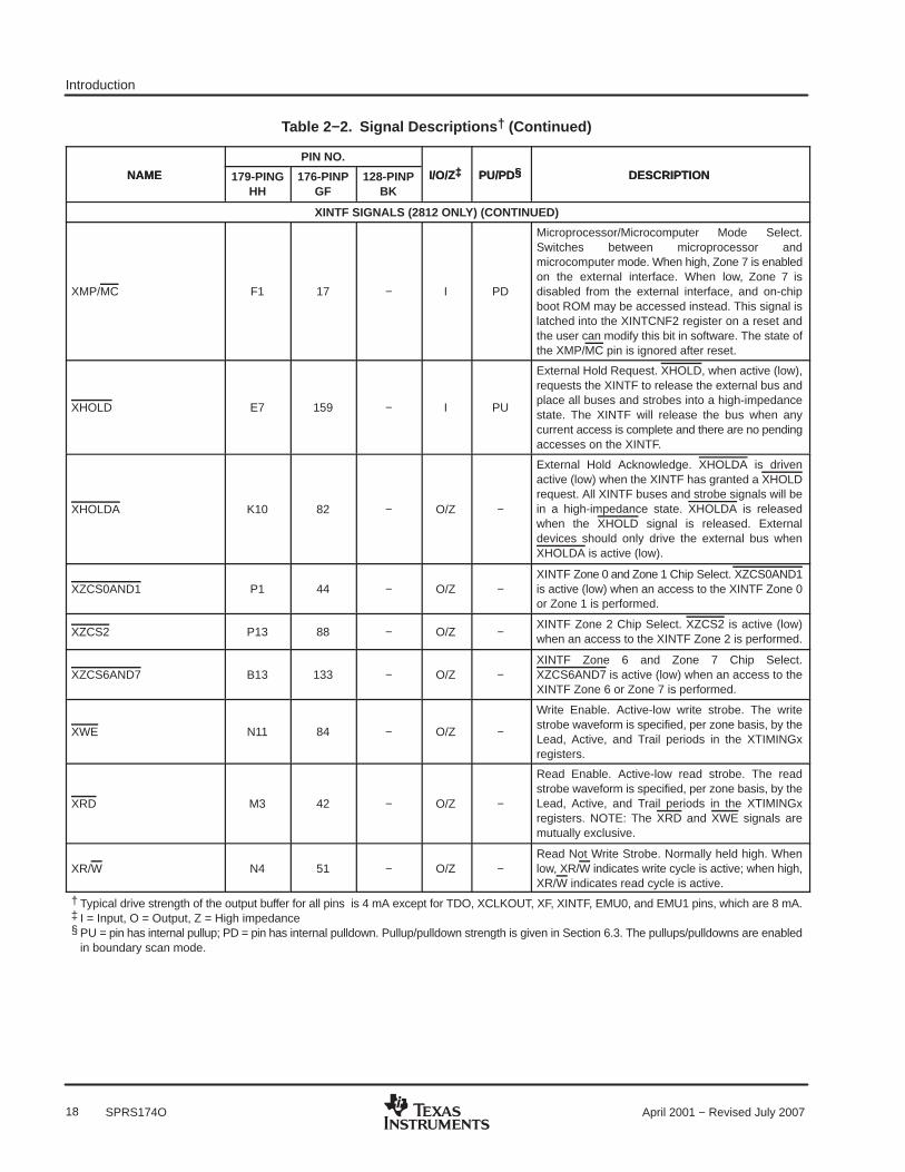
2.4 Signal Descriptions
Table 2−2 specifies the signals on the F281x and C281x devices. All digital inputs are TTL-compatible. Alloutputs are 3.3 V with CMOS levels. Inputs are not 5-V tolerant. A 100-µA (or 20-µA) pullup/pulldown is used.
Table 2−2. Signal Descriptions †
PIN NO.‡ §NAME 179-PING
HH176-PINP
GF128-PINP
BKI/O/Z‡ PU/PD§ DESCRIPTION
XINTF SIGNALS (2812 ONLY)
XA[18] D7 158 − O/Z −
XA[17] B7 156 − O/Z −
XA[16] A8 152 − O/Z −
XA[15] B9 148 − O/Z −
XA[14] A10 144 − O/Z −
XA[13] E10 141 − O/Z −
XA[12] C11 138 − O/Z −
XA[11] A14 132 − O/Z
XA[10] C12 130 − O/Z −
XA[9] D14 125 − O/Z − 19-bit XINTF Address Bus
XA[8] E12 121 − O/Z −
19-bit XINTF Address Bus
XA[7] F12 118 − O/Z −
XA[6] G14 111 − O/Z −
XA[5] H13 108 − O/Z −
XA[4] J12 103 − O/Z −
XA[3] M11 85 − O/Z −
XA[2] N10 80 − O/Z −
XA[1] M2 43 − O/Z −
XA[0] G5 18 − O/Z
XD[15] A9 147 − I/O/Z PU
XD[14] B11 139 − I/O/Z PU
XD[13] J10 97 − I/O/Z PU
XD[12] L14 96 − I/O/Z PU
XD[11] N9 74 − I/O/Z PU
XD[10] L9 73 − I/O/Z PU
XD[9] M8 68 − I/O/Z PU
XD[8] P7 65 − I/O/Z PU16-bit XINTF Data Bus
XD[7] L5 54 − I/O/Z PU16-bit XINTF Data Bus
XD[6] L3 39 − I/O/Z PU
XD[5] J5 36 − I/O/Z PU
XD[4] K3 33 − I/O/Z PU
XD[3] J3 30 − I/O/Z PU
XD[2] H5 27 − I/O/Z PU
XD[1] H3 24 − I/O/Z PU
XD[0] G3 21 − I/O/Z PU† Typical drive strength of the output buffer for all pins is 4 mA except for TDO, XCLKOUT, XF, XINTF, EMU0, and EMU1 pins, which are 8 mA.‡ I = Input, O = Output, Z = High impedance§ PU = pin has internal pullup; PD = pin has internal pulldown. Pullup/pulldown strength is given in Section 6.3. The pullups/pulldowns are enabled
in boundary scan mode.
Introduction
18 April 2001 − Revised July 2007SPRS174O
Table 2−2. Signal Descriptions † (Continued)
NAME DESCRIPTIONPU/PD§I/O/Z‡PIN NO.
NAME DESCRIPTIONPU/PD§I/O/Z‡128-PINPBK
176-PINPGF
179-PINGHH
XINTF SIGNALS (2812 ONLY) (CONTINUED)
XMP/MC F1 17 − I PD
Microprocessor/Microcomputer Mode Select.Switches between microprocessor andmicrocomputer mode. When high, Zone 7 is enabledon the external interface. When low, Zone 7 isdisabled from the external interface, and on-chipboot ROM may be accessed instead. This signal islatched into the XINTCNF2 register on a reset andthe user can modify this bit in software. The state ofthe XMP/MC pin is ignored after reset.
XHOLD E7 159 − I PU
External Hold Request. XHOLD, when active (low),requests the XINTF to release the external bus andplace all buses and strobes into a high-impedancestate. The XINTF will release the bus when anycurrent access is complete and there are no pendingaccesses on the XINTF.
XHOLDA K10 82 − O/Z −
External Hold Acknowledge. XHOLDA is drivenactive (low) when the XINTF has granted a XHOLDrequest. All XINTF buses and strobe signals will bein a high-impedance state. XHOLDA is releasedwhen the XHOLD signal is released. Externaldevices should only drive the external bus whenXHOLDA is active (low).
XZCS0AND1 P1 44 − O/Z −XINTF Zone 0 and Zone 1 Chip Select. XZCS0AND1is active (low) when an access to the XINTF Zone 0or Zone 1 is performed.
XZCS2 P13 88 − O/Z −XINTF Zone 2 Chip Select. XZCS2 is active (low)when an access to the XINTF Zone 2 is performed.
XZCS6AND7 B13 133 − O/Z −XINTF Zone 6 and Zone 7 Chip Select.XZCS6AND7 is active (low) when an access to theXINTF Zone 6 or Zone 7 is performed.
XWE N11 84 − O/Z −
Write Enable. Active-low write strobe. The writestrobe waveform is specified, per zone basis, by theLead, Active, and Trail periods in the XTIMINGxregisters.
XRD M3 42 − O/Z −
Read Enable. Active-low read strobe. The readstrobe waveform is specified, per zone basis, by theLead, Active, and Trail periods in the XTIMINGxregisters. NOTE: The XRD and XWE signals aremutually exclusive.
XR/W N4 51 − O/Z −Read Not Write Strobe. Normally held high. Whenlow, XR/W indicates write cycle is active; when high,XR/W indicates read cycle is active.
† Typical drive strength of the output buffer for all pins is 4 mA except for TDO, XCLKOUT, XF, XINTF, EMU0, and EMU1 pins, which are 8 mA.‡ I = Input, O = Output, Z = High impedance§ PU = pin has internal pullup; PD = pin has internal pulldown. Pullup/pulldown strength is given in Section 6.3. The pullups/pulldowns are enabled
in boundary scan mode.

Introduction
19April 2001 − Revised July 2007 SPRS174O
Table 2−2. Signal Descriptions † (Continued)
NAME DESCRIPTIONPU/PD§I/O/Z‡PIN NO.
NAME DESCRIPTIONPU/PD§I/O/Z‡128-PINPBK
176-PINPGF
179-PINGHH
XINTF SIGNALS (2812 ONLY) (CONTINUED)
XREADY B6 161 − I PU
Ready Signal. Indicates peripheral is ready tocomplete the access when asserted to 1. XREADYcan be configured to be a synchronous or anasynchronous input. See the timing diagrams formore details.
JTAG AND MISCELLANEOUS SIGNALS
X1/XCLKIN K9 77 58 I
Oscillator Input − input to the internal oscillator. Thispin is also used to feed an external clock. The 28xcan be operated with an external clock source,provided that the proper voltage levels be driven onthe X1/XCLKIN pin. It should be noted that theX1/XCLKIN pin is referenced to the 1.8-V (or 1.9-V)core digital power supply (VDD), rather than the3.3-V I/O supply (VDDIO). A clamping diode may beused to clamp a buffered clock signal to ensure thatthe logic-high level does not exceed VDD (1.8 V or1.9 V) or a 1.8-V oscillator may be used.
X2 M9 76 57 O Oscillator Output
XCLKOUT F11 119 87 O −
Output clock derived from SYSCLKOUT to be usedfor external wait-state generation and as ageneral-purpose clock source. XCLKOUT is eitherthe same frequency, 1/2 the frequency, or 1/4 thefrequency of SYSCLKOUT. At reset, XCLKOUT =SYSCLKOUT/4. The XCLKOUT signal can beturned off by setting bit 3 (CLKOFF) of theXINTCNF2 register to 1. Unlike other GPIO pins, theXCLKOUT pin is not placed in a high impedancestate during reset.
TESTSEL A13 134 97 I PDTest Pin. Reserved for TI. Must be connected toground.
XRS D6 160 113 I/O PU
Device Reset (in) and Watchdog Reset (out).
Device reset. XRS causes the device to terminateexecution. The PC will point to the addresscontained at the location 0x3FFFC0. When XRS isbrought to a high level, execution begins at thelocation pointed to by the PC. This pin is driven lowby the DSP when a watchdog reset occurs. Duringwatchdog reset, the XRS pin will be driven low for thewatchdog reset duration of 512 XCLKIN cycles.
The output buffer of this pin is an open-drain with aninternal pullup (100 µA, typical). It is recommendedthat this pin be driven by an open-drain device.
† Typical drive strength of the output buffer for all pins is 4 mA except for TDO, XCLKOUT, XF, XINTF, EMU0, and EMU1 pins, which are 8 mA.‡ I = Input, O = Output, Z = High impedance§ PU = pin has internal pullup; PD = pin has internal pulldown. Pullup/pulldown strength is given in Section 6.3. The pullups/pulldowns are enabled
in boundary scan mode.
Introduction
20 April 2001 − Revised July 2007SPRS174O
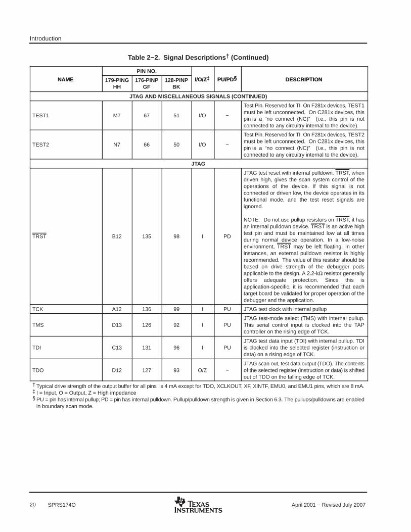
Table 2−2. Signal Descriptions † (Continued)
NAME DESCRIPTIONPU/PD§I/O/Z‡PIN NO.
NAME DESCRIPTIONPU/PD§I/O/Z‡128-PINPBK
176-PINPGF
179-PINGHH
JTAG AND MISCELLANEOUS SIGNALS (CONTINUED)
TEST1 M7 67 51 I/O −
Test Pin. Reserved for TI. On F281x devices, TEST1must be left unconnected. On C281x devices, thispin is a “no connect (NC)” (i.e., this pin is notconnected to any circuitry internal to the device).
TEST2 N7 66 50 I/O −
Test Pin. Reserved for TI. On F281x devices, TEST2must be left unconnected. On C281x devices, thispin is a “no connect (NC)” (i.e., this pin is notconnected to any circuitry internal to the device).
JTAG
TRST B12 135 98 I PD
JTAG test reset with internal pulldown. TRST, whendriven high, gives the scan system control of theoperations of the device. If this signal is notconnected or driven low, the device operates in itsfunctional mode, and the test reset signals areignored.
NOTE: Do not use pullup resistors on TRST; it hasan internal pulldown device. TRST is an active hightest pin and must be maintained low at all timesduring normal device operation. In a low-noiseenvironment, TRST may be left floating. In otherinstances, an external pulldown resistor is highlyrecommended. The value of this resistor should bebased on drive strength of the debugger podsapplicable to the design. A 2.2-kΩ resistor generallyoffers adequate protection. Since this isapplication-specific, it is recommended that eachtarget board be validated for proper operation of thedebugger and the application.
TCK A12 136 99 I PU JTAG test clock with internal pullup
TMS D13 126 92 I PUJTAG test-mode select (TMS) with internal pullup.This serial control input is clocked into the TAPcontroller on the rising edge of TCK.
TDI C13 131 96 I PUJTAG test data input (TDI) with internal pullup. TDIis clocked into the selected register (instruction ordata) on a rising edge of TCK.
TDO D12 127 93 O/Z −JTAG scan out, test data output (TDO). The contentsof the selected register (instruction or data) is shiftedout of TDO on the falling edge of TCK.
† Typical drive strength of the output buffer for all pins is 4 mA except for TDO, XCLKOUT, XF, XINTF, EMU0, and EMU1 pins, which are 8 mA.‡ I = Input, O = Output, Z = High impedance§ PU = pin has internal pullup; PD = pin has internal pulldown. Pullup/pulldown strength is given in Section 6.3. The pullups/pulldowns are enabled
in boundary scan mode.
Introduction
21April 2001 − Revised July 2007 SPRS174O
Table 2−2. Signal Descriptions † (Continued)
NAME DESCRIPTIONPU/PD§I/O/Z‡PIN NO.
NAME DESCRIPTIONPU/PD§I/O/Z‡128-PINPBK
176-PINPGF
179-PINGHH
JTAG (CONTINUED)
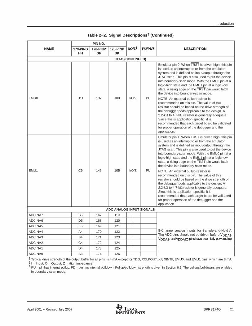
EMU0 D11 137 100 I/O/Z PU
Emulator pin 0. When TRST is driven high, this pinis used as an interrupt to or from the emulatorsystem and is defined as input/output through theJTAG scan. This pin is also used to put the deviceinto boundary-scan mode. With the EMU0 pin at alogic-high state and the EMU1 pin at a logic-lowstate, a rising edge on the TRST pin would latchthe device into boundary-scan mode.
NOTE: An external pullup resistor isrecommended on this pin. The value of thisresistor should be based on the drive strength ofthe debugger pods applicable to the design. A2.2-kΩ to 4.7-kΩ resistor is generally adequate.Since this is application-specific, it isrecommended that each target board be validatedfor proper operation of the debugger and theapplication.
EMU1 C9 146 105 I/O/Z PU
Emulator pin 1. When TRST is driven high, this pinis used as an interrupt to or from the emulatorsystem and is defined as input/output through theJTAG scan. This pin is also used to put the deviceinto boundary-scan mode. With the EMU0 pin at alogic-high state and the EMU1 pin at a logic-lowstate, a rising edge on the TRST pin would latchthe device into boundary-scan mode.
NOTE: An external pullup resistor isrecommended on this pin. The value of thisresistor should be based on the drive strength ofthe debugger pods applicable to the design. A2.2-kΩ to 4.7-kΩ resistor is generally adequate.Since this is application-specific, it isrecommended that each target board be validatedfor proper operation of the debugger and theapplication.
ADC ANALOG INPUT SIGNALS
ADCINA7 B5 167 119 I
ADCINA6 D5 168 120 I
ADCINA5 E5 169 121 I8-Channel analog inputs for Sample-and-Hold A.ADCINA4 A4 170 122 I 8-Channel analog inputs for Sample-and-Hold A.The ADC pins should not be driven before VDDA1,
ADCINA3 B4 171 123 IThe ADC pins should not be driven before VDDA1,VDDA2, and VDDAIO pins have been fully powered up.
ADCINA2 C4 172 124 IVDDA2, and VDDAIO pins have been fully powered up.
ADCINA1 D4 173 125 I
ADCINA0 A3 174 126 I† Typical drive strength of the output buffer for all pins is 4 mA except for TDO, XCLKOUT, XF, XINTF, EMU0, and EMU1 pins, which are 8 mA.‡ I = Input, O = Output, Z = High impedance§ PU = pin has internal pullup; PD = pin has internal pulldown. Pullup/pulldown strength is given in Section 6.3. The pullups/pulldowns are enabled
in boundary scan mode.

Introduction
22 April 2001 − Revised July 2007SPRS174O
Table 2−2. Signal Descriptions † (Continued)
NAME DESCRIPTIONPU/PD§I/O/Z‡PIN NO.
NAME DESCRIPTIONPU/PD§I/O/Z‡128-PINPBK
176-PINPGF
179-PINGHH
ADC ANALOG INPUT SIGNALS (CONTINUED)
ADCINB7 F5 9 9 I
ADCINB6 D1 8 8 I
ADCINB5 D2 7 7 I8-Channel Analog Inputs for Sample-and-Hold B.
ADCINB4 D3 6 6 I8-Channel Analog Inputs for Sample-and-Hold B.The ADC pins should not be driven before the
ADCINB3 C1 5 5 IThe ADC pins should not be driven before theVDDA1, VDDA2, and VDDAIO pins have been fullypowered up.
ADCINB2 B1 4 4 I
VDDA1, VDDA2, and VDDAIO pins have been fullypowered up.
ADCINB1 C3 3 3 I
ADCINB0 C2 2 2 I
ADCREFP E2 11 11 I/O
ADC Voltage Reference Output (2 V). Requires alow ESR (50 mΩ − 1.5 Ω) ceramic bypass capacitorof 10 µF to analog ground. (Can accept externalreference input (2 V) if the software bit is enabled forthis mode. 1−10 µF low ESR capacitor can be usedin the external reference mode.)
ADCREFM E4 10 10 I/O
ADC Voltage Reference Output (1 V). Requires alow ESR (50 mΩ − 1.5 Ω) ceramic bypass capacitorof 10 µF to analog ground. (Can accept externalreference input (1 V) if the software bit is enabled forthis mode. 1−10 µF low ESR capacitor can be usedin the external reference mode.)
ADCRESEXT F2 16 16 OADC External Current Bias Resistor Use 24.9 kΩ ±5% for ADC clock range 1 − 18.75 MHz
20 kΩ ±5% for ADC clock range 18.75 MHz − 25 MHz
ADCBGREFIN E6 164 116 Test Pin. Reserved for TI. Must be left unconnected.
AVSSREFBG E3 12 12 ADC Analog GND
AVDDREFBG E1 13 13 ADC Analog Power (3.3-V)
ADCLO B3 175 127Common Low Side Analog Input. Connect to analogground.
VSSA1 F3 15 15 ADC Analog GND
VSSA2 C5 165 117 ADC Analog GND
VDDA1 F4 14 14 ADC Analog 3.3-V Supply
VDDA2 A5 166 118 ADC Analog 3.3-V Supply
VSS1 C6 163 115 ADC Digital GND
VDD1 A6 162 114 ADC Digital 1.8-V (or 1.9-V) Supply
VDDAIO B2 1 1 3.3-V Analog I/O Power Pin
VSSAIO A2 176 128 Analog I/O Ground Pin† Typical drive strength of the output buffer for all pins is 4 mA except for TDO, XCLKOUT, XF, XINTF, EMU0, and EMU1 pins, which are 8 mA.‡ I = Input, O = Output, Z = High impedance§ PU = pin has internal pullup; PD = pin has internal pulldown. Pullup/pulldown strength is given in Section 6.3. The pullups/pulldowns are enabled
in boundary scan mode.

Introduction
23April 2001 − Revised July 2007 SPRS174O
Table 2−2. Signal Descriptions † (Continued)
NAME DESCRIPTIONPU/PD§I/O/Z‡PIN NO.
NAME DESCRIPTIONPU/PD§I/O/Z‡128-PINPBK
176-PINPGF
179-PINGHH
POWER SIGNALS
VDD H1 23 20
VDD L1 37 29
VDD P5 56 42
VDD P9 75 561.8-V or 1.9-V Core Digital Power Pins. SeeVDD P12 − 63 1.8-V or 1.9-V Core Digital Power Pins. SeeSection 6.2, Recommended Operating Conditions,
VDD K12 100 74Section 6.2, Recommended Operating Conditions,for voltage requirements.
VDD G12 112 82for voltage requirements.
VDD C14 128 94
VDD B10 143 102
VDD C8 154 110
VSS G4 19 17
VSS K1 32 26
VSS L2 38 30
VSS P4 52 39
VSS K6 58 −
VSS P8 70 53
VSS M10 78 59
VSS L11 86 62Core and Digital I/O Ground Pins
VSS K13 99 73Core and Digital I/O Ground Pins
VSS J14 105 −
VSS G13 113 −
VSS E14 120 88
VSS B14 129 95
VSS D10 142 −
VSS C10 − 103
VSS B8 153 109
VDDIO J4 31 25
VDDIO L7 64 49
VDDIO L10 81 −3.3-V I/O Digital Power Pins
VDDIO N14 − −3.3-V I/O Digital Power Pins
VDDIO G11 114 83
VDDIO E9 145 104
VDD3VFL N8 69 52
3.3-V Flash Core Power Pin. This pin should beconnected to 3.3 V at all times after power-upsequence requirements have been met. This pin isused as VDDIO in ROM parts and must beconnected to 3.3 V in ROM parts as well.
† Typical drive strength of the output buffer for all pins is 4 mA except for TDO, XCLKOUT, XF, XINTF, EMU0, and EMU1 pins, which are 8 mA.‡ I = Input, O = Output, Z = High impedance§ PU = pin has internal pullup; PD = pin has internal pulldown. Pullup/pulldown strength is given in Section 6.3. The pullups/pulldowns are enabled
in boundary scan mode.
Introduction
24 April 2001 − Revised July 2007SPRS174O
Table 2−2. Signal Descriptions † (Continued)
NAME DESCRIPTIONPU/PD§I/O/Z‡PIN NO.
NAME DESCRIPTIONPU/PD§I/O/Z‡128-PINPBK
176-PINPGF
179-PINGHH
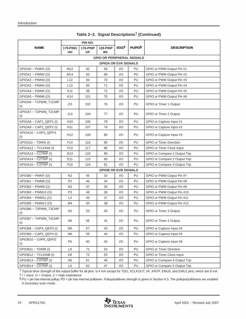
GPIO OR PERIPHERAL SIGNALS
GPIOA OR EVA SIGNALS
GPIOA0 − PWM1 (O) M12 92 68 I/O PU GPIO or PWM Output Pin #1
GPIOA1 − PWM2 (O) M14 93 69 I/O PU GPIO or PWM Output Pin #2
GPIOA2 − PWM3 (O) L12 94 70 I/O PU GPIO or PWM Output Pin #3
GPIOA3 − PWM4 (O) L13 95 71 I/O PU GPIO or PWM Output Pin #4
GPIOA4 − PWM5 (O) K11 98 72 I/O PU GPIO or PWM Output Pin #5
GPIOA5 − PWM6 (O) K14 101 75 I/O PU GPIO or PWM Output Pin #6
GPIOA6 − T1PWM_T1CMP(I)
J11 102 76 I/O PU GPIO or Timer 1 Output
GPIOA7 − T2PWM_T2CMP(I)
J13 104 77 I/O PU GPIO or Timer 2 Output
GPIOA8 − CAP1_QEP1 (I) H10 106 78 I/O PU GPIO or Capture Input #1
GPIOA9 − CAP2_QEP2 (I) H11 107 79 I/O PU GPIO or Capture Input #2
GPIOA10 − CAP3_QEPI1(I)
H12 109 80 I/O PU GPIO or Capture Input #3
GPIOA11 − TDIRA (I) F14 116 85 I/O PU GPIO or Timer Direction
GPIOA12 − TCLKINA (I) F13 117 86 I/O PU GPIO or Timer Clock Input
GPIOA13 − C1TRIP (I) E13 122 89 I/O PU GPIO or Compare 1 Output Trip
GPIOA14 − C2TRIP (I) E11 123 90 I/O PU GPIO or Compare 2 Output Trip
GPIOA15 − C3TRIP (I) F10 124 91 I/O PU GPIO or Compare 3 Output Trip
GPIOB OR EVB SIGNALS
GPIOB0 − PWM7 (O) N2 45 33 I/O PU GPIO or PWM Output Pin #7
GPIOB1 − PWM8 (O) P2 46 34 I/O PU GPIO or PWM Output Pin #8
GPIOB2 − PWM9 (O) N3 47 35 I/O PU GPIO or PWM Output Pin #9
GPIOB3 − PWM10 (O) P3 48 36 I/O PU GPIO or PWM Output Pin #10
GPIOB4 − PWM11 (O) L4 49 37 I/O PU GPIO or PWM Output Pin #11
GPIOB5 − PWM12 (O) M4 50 38 I/O PU GPIO or PWM Output Pin #12
GPIOB6 − T3PWM_T3CMP(I)
K5 53 40 I/O PU GPIO or Timer 3 Output
GPIOB7 − T4PWM_T4CMP(I)
N5 55 41 I/O PU GPIO or Timer 4 Output
GPIOB8 − CAP4_QEP3 (I) M5 57 43 I/O PU GPIO or Capture Input #4
GPIOB9 − CAP5_QEP4 (I) M6 59 44 I/O PU GPIO or Capture Input #5
GPIOB10 − CAP6_QEPI2(I)
P6 60 45 I/O PU GPIO or Capture Input #6
GPIOB11 − TDIRB (I) L8 71 54 I/O PU GPIO or Timer Direction
GPIOB12 − TCLKINB (I) K8 72 55 I/O PU GPIO or Timer Clock Input
GPIOB13 − C4TRIP (I) N6 61 46 I/O PU GPIO or Compare 4 Output Trip
GPIOB14 − C5TRIP (I) L6 62 47 I/O PU GPIO or Compare 5 Output Trip† Typical drive strength of the output buffer for all pins is 4 mA except for TDO, XCLKOUT, XF, XINTF, EMU0, and EMU1 pins, which are 8 mA.‡ I = Input, O = Output, Z = High impedance§ PU = pin has internal pullup; PD = pin has internal pulldown. Pullup/pulldown strength is given in Section 6.3. The pullups/pulldowns are enabled
in boundary scan mode.
Introduction
25April 2001 − Revised July 2007 SPRS174O
Table 2−2. Signal Descriptions † (Continued)
NAME DESCRIPTIONPU/PD§I/O/Z‡PIN NO.
NAME DESCRIPTIONPU/PD§I/O/Z‡128-PINPBK
176-PINPGF
179-PINGHH
GPIOB15 − C6TRIP (I) K7 63 48 I/O PU GPIO or Compare 6 Output Trip† Typical drive strength of the output buffer for all pins is 4 mA except for TDO, XCLKOUT, XF, XINTF, EMU0, and EMU1 pins, which are 8 mA.‡ I = Input, O = Output, Z = High impedance§ PU = pin has internal pullup; PD = pin has internal pulldown. Pullup/pulldown strength is given in Section 6.3. The pullups/pulldowns are enabled
in boundary scan mode.
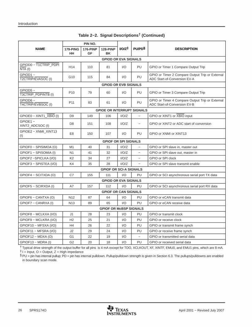
Introduction
26 April 2001 − Revised July 2007SPRS174O
Table 2−2. Signal Descriptions † (Continued)
NAME DESCRIPTIONPU/PD§I/O/Z‡PIN NO.
NAME DESCRIPTIONPU/PD§I/O/Z‡128-PINPBK
176-PINPGF
179-PINGHH
GPIOD OR EVA SIGNALS
GPIOD0 − T1CTRIP_PDPINTA (I)
H14 110 81 I/O PU GPIO or Timer 1 Compare Output Trip
GPIOD1 −T2CTRIP/EVASOC (I)
G10 115 84 I/O PUGPIO or Timer 2 Compare Output Trip or ExternalADC Start-of-Conversion EV-A
GPIOD OR EVB SIGNALS
GPIOD5 −T3CTRIP_PDPINTB (I)
P10 79 60 I/O PU GPIO or Timer 3 Compare Output Trip
GPIOD6 −T4CTRIP/EVBSOC (I)
P11 83 61 I/O PUGPIO or Timer 4 Compare Output Trip or ExternalADC Start-of-Conversion EV-B
GPIOE OR INTERRUPT SIGNALS
GPIOE0 − XINT1_XBIO (I) D9 149 106 I/O/Z − GPIO or XINT1 or XBIO input
GPIOE1 −XINT2_ADCSOC (I)
D8 151 108 I/O/Z − GPIO or XINT2 or ADC start of conversion
GPIOE2 − XNMI_XINT13(I)
E8 150 107 I/O PU GPIO or XNMI or XINT13
GPIOF OR SPI SIGNALS
GPIOF0 − SPISIMOA (O) M1 40 31 I/O/Z − GPIO or SPI slave in, master out
GPIOF1 − SPISOMIA (I) N1 41 32 I/O/Z − GPIO or SPI slave out, master in
GPIOF2 −SPICLKA (I/O) K2 34 27 I/O/Z − GPIO or SPI clock
GPIOF3 − SPISTEA (I/O) K4 35 28 I/O/Z − GPIO or SPI slave transmit enable
GPIOF OR SCI-A SIGNALS
GPIOF4 − SCITXDA (O) C7 155 111 I/O PU GPIO or SCI asynchronous serial port TX data
GPIOD OR EVA SIGNALS
GPIOF5 − SCIRXDA (I) A7 157 112 I/O PU GPIO or SCI asynchronous serial port RX data
GPIOF OR CAN SIGNALS
GPIOF6 − CANTXA (O) N12 87 64 I/O PU GPIO or eCAN transmit data
GPIOF7 − CANRXA (I) N13 89 65 I/O PU GPIO or eCAN receive data
GPIOF OR McBSP SIGNALS
GPIOF8 − MCLKXA (I/O) J1 28 23 I/O PU GPIO or transmit clock
GPIOF9 − MCLKRA (I/O) H2 25 21 I/O PU GPIO or receive clock
GPIOF10 − MFSXA (I/O) H4 26 22 I/O PU GPIO or transmit frame synch
GPIOF11 − MFSRA (I/O) J2 29 24 I/O PU GPIO or receive frame synch
GPIOF12 − MDXA (O) G1 22 19 I/O − GPIO or transmitted serial data
GPIOF13 − MDRA (I) G2 20 18 I/O PU GPIO or received serial data† Typical drive strength of the output buffer for all pins is 4 mA except for TDO, XCLKOUT, XF, XINTF, EMU0, and EMU1 pins, which are 8 mA.‡ I = Input, O = Output, Z = High impedance§ PU = pin has internal pullup; PD = pin has internal pulldown. Pullup/pulldown strength is given in Section 6.3. The pullups/pulldowns are enabled
in boundary scan mode.

Introduction
27April 2001 − Revised July 2007 SPRS174O
Table 2−2. Signal Descriptions † (Continued)
NAME DESCRIPTIONPU/PD§I/O/Z‡PIN NO.
NAME DESCRIPTIONPU/PD§I/O/Z‡128-PINPBK
176-PINPGF
179-PINGHH
GPIOF OR XF CPU OUTPUT SIGNAL
GPIOF14 − XF_XPLLDIS(O)
A11 140 101 I/O PU
This pin has three functions:1. XF − General-purpose output pin.2. XPLLDIS − This pin is sampled during reset
to check whether the PLL must be disabled.The PLL will be disabled if this pin is sensedlow. HALT and STANDBY modes cannot be used when the PLL is disabled.
3. GPIO − GPIO function
GPIOG OR SCI-B SIGNALS
GPIOG4 − SCITXDB (O) P14 90 66 I/O/Z − GPIO or SCI asynchronous serial port transmit data
GPIOG5 − SCIRXDB (I) M13 91 67 I/O/Z − GPIO or SCI asynchronous serial port receive data
† Typical drive strength of the output buffer for all pins is 4 mA except for TDO, XCLKOUT, XF, XINTF, EMU0, and EMU1 pins, which are 8 mA.‡ I = Input, O = Output, Z = High impedance§ PU = pin has internal pullup; PD = pin has internal pulldown. Pullup/pulldown strength is given in Section 6.3. The pullups/pulldowns are enabled
in boundary scan mode.
NOTE: Other than the power supply pins, no pin should be driven before the 3.3-V rail has reachedrecommended operating conditions. However, it is acceptable for an I/O pin to ramp along withthe 3.3-V supply.

Functional Overview
28 April 2001 − Revised July 2007SPRS174O
3 Functional Overview
ÍÍÍÍÍÍÍÍÍÍÍÍÍÍÍÍÍÍÍÍÍÍÍÍ
ÍÍÍÍÍÍÍÍÍÍÍÍÍÍÍÍÍÍ
ÍÍÍÍÍÍÍÍÍÍÍÍÍÍÍÍÍÍÍÍÍÍÍÍÍÍÍÍÍÍ
M0 SARAM1K x 16
CPU-Timer 0
CPU-Timer 1
INT[12:1]
CLKIN
Real-Time JTAGCPU-Timer 2
Peripheral Bus
C28x CPU
H0 SARAM8K × 16
INT14
NMI
INT13
Memory Bus
M1 SARAM1K x 16
Flash128K x 16 (F2812)128K x 16 (F2811)64K x 16 (F2810)
Boot ROM4K × 16
eCAN
SCIA/SCIB
12-Bit ADC
External InterruptControl
(XINT1/2/13, XNMI)
EVA/EVB
Memory Bus
OTP(C)
1K x 16
McBSP
System Control
(Oscillator and PLL+
Peripheral Clocking+
Low-PowerModes
+WatchDog)
FIFO
FIFO
PIE(96 interrupts) (A)
RS
SPI FIFO
TINT0
TINT1
TINT2 Control
Address(19)
Data(16)
ExternalInterface(XINTF)(B)
16 Channels
NOTES: A. 45 of the possible 96 interrupts are used on the devices.B. XINTF is available on the F2812 and C2812 devices only.C. On C281x devices, the OTP is replaced with a 1K X 16 block of ROM
GPIO Pins
XRS
X1/XCLKIN
X2
XF_XPLLDIS
ÍÍÍÍÍÍ
Protected by the code-security module.
XINT13
G
P
I
O
M
U
X
L1 SARAM4K x 16
XNMI
L0 SARAM4K x 16
ÍÍÍÍÍÍÍÍÍÍÍÍÍÍÍÍÍÍÍÍÍÍÍÍ
ROM128K x 16 (C2812)128K x 16 (C2811)64K x 16 (C2810)
Figure 3−1. Functional Block Diagram

Functional Overview
29April 2001 − Revised July 2007 SPRS174O
3.1 Memory Map
ÍÍÍÍÍÍÍÍÍÍÍÍÍÍÍÍÍÍÍÍÍÍÍÍÍÍÍÍÍÍÍÍÍÍÍÍÍÍÍÍÍÍÍÍÍÍÍÍÍÍÍÍÍÍÍÍÍÍÍÍÍÍÍÍÍÍÍÍÍÍÍÍÍÍÍÍÍÍÍÍÍÍÍÍÍÍÍÍÍÍÍÍÍÍÍÍ
ÍÍÍÍÍÍÍÍÍÍÍÍÍÍÍÍÍÍÍÍÍÍÍÍÍÍÍÍÍÍÍÍÍÍÍÍÍÍÍÍÍÍÍÍÍÍÍÍÍÍÍÍÍÍÍÍÍÍÍÍÍÍÍÍÍÍÍÍÍÍÍÍÍÍÍÍÍÍÍÍÍÍÍÍÍÍÍÍÍÍÍÍÍÍÍÍÍÍÍÍÍÍÍÍÍÍÍÍÍÍÍÍÍÍÍÍÍÍÍÍ
ÍÍÍÍÍÍÍÍÍÍÍÍÍÍÍÍÍÍÍÍÍÍÍÍÍÍÍÍÍÍÍÍÍ
ÍÍÍÍÍÍÍÍÍÍÍÍÍÍÍÍÍÍÍÍÍÍÍÍÍÍÍÍÍÍÍÍÍÍÍÍÍÍÍÍÍÍÍÍÍÍÍÍÍÍÍÍÍÍÍÍÍÍÍÍÍÍÍÍÍÍ
ÍÍÍÍÍÍÍÍÍÍÍÍÍÍÍÍÍÍÍÍÍÍÍÍÍÍÍÍÍÍÍÍÍ
BlockStart Address
Low
64K
(24x
/240
x E
quiv
alen
t Dat
a S
pace
)
0x00 0000 M0 Vector − RAM (32 × 32)(Enabled if VMAP = 0)
Data Space Prog Space
M0 SARAM (1K × 16)
M1 SARAM (1K × 16)ÍÍÍÍÍÍÍÍÍÍÍÍÍÍÍÍÍÍÍÍÍÍÍÍÍÍÍÍÍÍÍÍÍÍÍÍ
Peripheral Frame 0
0x00 0040
0x00 0400
0x00 0800
PIE Vector - RAM (256 × 16)
(Enabled if VMAP= 1, ENPIE = 1)
ÍÍÍÍÍÍÍÍÍÍÍÍ
Reserved
Reserved
Reserved
L0 SARAM (4K × 16, Secure Block)
Peripheral Frame 1(Protected) ÍÍÍÍÍÍ
ÍÍÍÍÍÍÍÍÍÍÍÍÍÍÍÍÍÍ
ReservedPeripheral Frame 2
(Protected)
L1 SARAM (4K × 16, Secure Block)
Reserved
OTP (or ROM) (1K × 16, Secure Block)
Flash (or ROM) (128K × 16, Secure Block)
128-Bit Password
H0 SARAM (8K × 16)
Reserved
Boot ROM (4K × 16)(Enabled if MP/MC = 0)
BROM Vector - ROM (32 × 32)(Enabled if VMAP = 1, MP/MC = 0, ENPIE = 0)
0x00 0D00
0x00 0E00
0x00 2000
0x00 6000
0x00 7000
0x00 8000
0x00 9000
0x00 A000
0x3D 7800
0x3D 7C00
0x3F 7FF8
0x3F 8000
0x3F A000
0x3F F000
0x3F FFC0
Hig
h 64
K(2
4x/2
40x
Equ
ival
ent
Pro
gram
Spa
ce)
Data Space Prog Space
Reserved
XINTF Zone 0 (8K × 16, XZCS0AND1)
XINTF Zone 1 (8K × 16, XZCS0AND1) (Protected)
ÍÍÍÍÍÍÍÍÍÍÍÍÍÍÍÍÍÍÍÍÍÍÍÍÍÍÍÍÍÍÍÍÍÍÍÍÍÍÍÍÍÍÍÍÍÍÍÍÍÍÍÍÍÍÍÍÍÍÍÍÍÍÍÍÍÍÍÍÍÍÍÍ
Reserved
XINTF Zone 2 (0.5M × 16, XZCS2)
XINTF Zone 6 (0.5M × 16, XZCS6AND7)
Reserved
XINTF Zone 7 (16K × 16, XZCS6AND7)(Enabled if MP/MC = 1)
XINTF Vector - RAM (32 × 32)(Enabled if VMAP = 1, MP/MC = 1, ENPIE = 0)
On-Chip Memory External Memory XINTF
Only one of these vector maps—M0 vector, PIE vector, BROM vector, XINTF vector—should be enabled at a time.
LEGEND:
0x08 0000
0x00 4000
0x10 0000
0x18 0000
0x3F C000
0x00 2000
ÍÍÍÍÍÍÍÍÍÍÍReserved (1K)0x3D 8000
NOTES: A. Memory blocks are not to scale.B. Reserved locations are reserved for future expansion. Application should not access these areas.C. Boot ROM and Zone 7 memory maps are active either in on-chip or XINTF zone depending on MP/MC, not in both.D. Peripheral Frame 0, Peripheral Frame 1, and Peripheral Frame 2 memory maps are restricted to data memory only. User program
cannot access these memory maps in program space.E. “Protected” means the order of Write followed by Read operations is preserved rather than the pipeline order.F. Certain memory ranges are EALLOW protected against spurious writes after configuration.G. Zones 0 and 1 and Zones 6 and 7 share the same chip select; hence, these memory blocks have mirrored locations.
Figure 3−2. F2812/C2812 Memory Map

Functional Overview
30 April 2001 − Revised July 2007SPRS174O
ÍÍÍÍÍÍÍÍÍÍÍÍÍÍÍÍÍÍÍÍÍÍÍÍÍÍÍÍÍÍÍÍÍ
ÍÍÍÍÍÍÍÍÍÍÍÍÍÍÍÍÍÍÍÍÍÍÍÍÍÍÍÍÍÍÍÍÍÍÍÍÍÍÍÍÍÍÍÍÍÍÍÍÍÍÍÍÍÍÍÍÍÍÍÍÍÍÍÍÍÍ
ÍÍÍÍÍÍÍÍÍÍÍÍÍÍÍÍÍÍÍÍÍÍÍÍÍÍÍÍÍÍÍÍÍ
BlockStart Address
Low
64K
(24x
/240
x E
quiv
alen
t Dat
a S
pace
)
0x00 0000 M0 Vector − RAM (32 × 32)(Enabled if VMAP = 0)
Data Space Prog Space
M0 SARAM (1K × 16)
M1 SARAM (1K × 16)ÍÍÍÍÍÍÍÍÍÍÍÍÍÍÍÍÍÍÍÍÍÍÍÍÍÍÍÍÍÍÍÍÍÍÍÍ
Peripheral Frame 0
0x00 0040
0x00 0400
0x00 0800
PIE Vector - RAM (256 × 16)
(Enabled if VMAP= 1, ENPIE = 1)
ÍÍÍÍÍÍÍÍÍÍÍÍ
Reserved
Reserved
Reserved
L0 SARAM (4K × 16, Secure Block)
Peripheral Frame 1(Protected) ÍÍÍÍÍÍ
ÍÍÍÍÍÍÍÍÍÍÍÍÍÍÍÍÍÍ
ReservedPeripheral Frame 2
(Protected)
L1 SARAM (4K × 16, Secure Block)
Reserved
OTP (or ROM) (1K × 16, Secure Block)
Flash (or ROM) (128K × 16, Secure Block)
128-Bit Password
H0 SARAM (8K × 16)
Reserved
Boot ROM (4K × 16)(Enabled if MP/MC = 0)
BROM Vector - ROM (32 × 32)(Enabled if VMAP = 1, MP/MC = 0, ENPIE = 0)
0x00 0D00
0x00 0E00
0x00 2000
0x00 6000
0x00 7000
0x00 8000
0x00 9000
0x00 A000
0x3D 7800
0x3D 7C00
0x3F 7FF8
0x3F 8000
0x3F A000
0x3F F000
0x3F FFC0
Hig
h 64
K(2
4x/2
40x
Equ
ival
ent
Pro
gram
Spa
ce)
On-Chip Memory
Only one of these vector maps—M0 vector, PIE vector, BROM vector, XINTF vector—should be enabled at a time.
LEGEND:
ÍÍÍÍÍÍÍÍÍÍÍReserved (1K)0x3D 8000
NOTES: A. Memory blocks are not to scale.B. Reserved locations are reserved for future expansion. Application should not access these areas.C. Peripheral Frame 0, Peripheral Frame 1, and Peripheral Frame 2 memory maps are restricted to data memory only. User program
cannot access these memory maps in program space.D. “Protected” means the order of Write followed by Read operations is preserved rather than the pipeline order.E. Certain memory ranges are EALLOW protected against spurious writes after configuration.
Figure 3−3. F2811/C2811 Memory Map

Functional Overview
31April 2001 − Revised July 2007 SPRS174O
ÍÍÍÍÍÍÍÍÍÍÍÍÍÍÍÍÍÍÍÍÍÍ
ÍÍÍÍÍÍÍÍÍÍÍÍÍÍÍÍÍÍÍÍÍÍÍÍÍÍÍÍÍÍÍÍÍ
ÍÍÍÍÍÍÍÍÍÍÍÍÍÍÍÍÍÍÍÍÍÍÍÍÍÍÍÍÍÍÍÍÍÍÍÍÍÍÍÍÍÍÍÍÍÍÍÍÍÍÍÍÍÍÍ
ÍÍÍÍÍÍÍÍÍÍÍÍÍÍÍÍÍÍÍÍÍÍÍÍÍÍÍÍÍÍÍÍÍ
BlockStart Address
Low
64K
(24x
/240
x E
quiv
alen
t Dat
a S
pace
)
0x00 0000 M0 Vector − RAM (32 × 32)(Enabled if VMAP = 0)
Data Space Prog Space
M0 SARAM (1K × 16)
M1 SARAM (1K × 16)ÍÍÍÍÍÍÍÍÍÍÍÍÍÍÍÍÍÍÍÍÍÍÍÍÍÍÍÍÍÍÍÍÍÍÍÍ
Peripheral Frame 0
0x00 0040
0x00 0400
0x00 0800
PIE Vector - RAM (256 × 16)
(Enabled if VMAP= 1, ENPIE = 1)
ÍÍÍÍÍÍÍÍÍÍÍÍ
Reserved
Reserved
Reserved
L0 SARAM (4K × 16, Secure Block)
Peripheral Frame 1(Protected) ÍÍÍÍÍÍ
ÍÍÍÍÍÍÍÍÍÍÍÍÍÍÍÍÍÍ
ReservedPeripheral Frame 2
(Protected)
L1 SARAM (4K × 16, Secure Block)
Reserved
Reserved
Flash (or ROM) (64K × 16, Secure Block)
128-Bit Password
H0 SARAM (8K × 16)
Reserved
Boot ROM (4K × 16)(Enabled if MP/MC = 0)
BROM Vector - ROM (32 × 32)(Enabled if VMAP = 1, MP/MC = 0, ENPIE = 0)
0x00 0D00
0x00 0E00
0x00 2000
0x00 6000
0x00 7000
0x00 8000
0x00 9000
0x00 A000
0x3D 7C00
0x3E 8000
0x3F 7FF8
0x3F 8000
0x3F A000
0x3F F000
0x3F FFC0
Hig
h 64
K(2
4x/2
40x
Equ
ival
ent
Pro
gram
Spa
ce)
On-Chip Memory
Only one of these vector maps—M0 vector, PIE vector, BROM vector—should be enabled at a time.
LEGEND:
OTP (or ROM) (1K × 16, Secure Block)0x3D 7800
NOTES: A. Memory blocks are not to scale.B. Reserved locations are reserved for future expansion. Application should not access these areas.C. Peripheral Frame 0, Peripheral Frame 1, and Peripheral Frame 2 memory maps are restricted to data memory only. User program
cannot access these memory maps in program space.D. “Protected” means the order of Write followed by Read operations is preserved rather than the pipeline order.E. Certain memory ranges are EALLOW protected against spurious writes after configuration.
Figure 3−4. F2810/C2810 Memory Map

Functional Overview
32 April 2001 − Revised July 2007SPRS174O
Table 3−1. Addresses of Flash Sectors in F2812 and F2811
ADDRESS RANGE PROGRAM AND DATA SPACE
0x3D 80000x3D 9FFF
Sector J, 8K x 16
0x3D A0000x3D BFFF
Sector I, 8K x 16
0x3D C0000x3D FFFF
Sector H, 16K x 16
0x3E 00000x3E 3FFF
Sector G, 16K x 16
0x3E 40000x3E 7FFF
Sector F, 16K x 16
0x3E 80000x3E BFFF
Sector E, 16K x 16
0x3E C0000x3E FFFF
Sector D, 16K x 16
0x3F 00000x3F 3FFF
Sector C, 16K x 16
0x3F 40000x3F 5FFF
Sector B, 8K x 16
0x3F 6000 Sector A, 8K x 16
0x3F 7F800x3F 7FF5
Program to 0x0000 when using theCode Security Module
0x3F 7FF60x3F 7FF7
Boot-to-Flash (or ROM) Entry Point(program branch instruction here)
0x3F 7FF80x3F 7FFF
Security Password (128-Bit)(Do not program to all zeros)
Table 3−2. Addresses of Flash Sectors in F2810
ADDRESS RANGE PROGRAM AND DATA SPACE
0x3E 80000x3E BFFF
Sector E, 16K x 16
0x3E C0000x3E FFFF
Sector D, 16K x 16
0x3F 00000x3F 3FFF
Sector C, 16K x 16
0x3F 40000x3F 5FFF
Sector B, 8K x 16
0x3F 6000 Sector A, 8K x 16
0x3F 7F800x3F 7FF5
Program to 0x0000 when using theCode Security Module
0x3F 7FF60x3F 7FF7
Boot-to-Flash (or ROM) Entry Point(program branch instruction here)
0x3F 7FF80x3F 7FFF
Security Password (128-Bit)(Do not program to all zeros)

Functional Overview
33April 2001 − Revised July 2007 SPRS174O
The “Low 64K” of the memory address range maps into the data space of the 240x. The “High 64K” of thememory address range maps into the program space of the 24x/240x. 24x/240x-compatible code will executeonly from the “High 64K” memory area. Hence, the top 32K of Flash/ROM and H0 SARAM block can be usedto run 24x/240x-compatible code (if MP/MC mode is low) or, on the 2812, code can be executed from XINTFZone 7 (if MP/MC mode is high).
The XINTF consists of five independent zones. One zone has its own chip select and the remaining four zonesshare two chip selects. Each zone can be programmed with its own timing (wait states) and to either sampleor ignore external ready signal. This makes interfacing to external peripherals easy and glueless.
NOTE: The chip selects of XINTF Zone 0 and Zone 1 are merged into a single chip select(XZCS0AND1); and the chip selects of XINTF Zone 6 and Zone 7 are merged into a single chipselect (XZCS6AND7). See Section 3.5, “External Interface, XINTF (2812 only)”, for details.
Peripheral Frame 1, Peripheral Frame 2, and XINTF Zone 1 are grouped together to enable these blocks tobe “write/read peripheral block protected”. The “protected” mode ensures that all accesses to these blockshappen as written. Because of the C28x pipeline, a write immediately followed by a read, to different memorylocations, will appear in reverse order on the memory bus of the CPU. This can cause problems in certainperipheral applications where the user expected the write to occur first (as written). The C28x CPU supportsa block protection mode where a region of memory can be protected to make sure that operations occur aswritten (the penalty is extra cycles that are added to align the operations). This mode is programmable and,by default, it will protect the selected zones.
On the 2812, at reset, XINTF Zone 7 is accessed if the XMP/MC pin is pulled high. This signal selectsmicroprocessor or microcomputer mode of operation. In microprocessor mode, Zone 7 is mapped to highmemory such that the vector table is fetched externally. The Boot ROM is disabled in this mode. Inmicrocomputer mode, Zone 7 is disabled such that the vectors are fetched from Boot ROM. This allows theuser to either boot from on-chip memory or from off-chip memory. The state of the XMP/MC signal on resetis stored in an MP/MC mode bit in the XINTCNF2 register. The user can change this mode in software andhence control the mapping of Boot ROM and XINTF Zone 7. No other memory blocks are affected byXMP/MC.
I/O space is not supported on the 2812 XINTF.
The wait states for the various spaces in the memory map area are listed in Table 3−3.

Functional Overview
34 April 2001 − Revised July 2007SPRS174O
Table 3−3. Wait States
AREA WAIT-STATES COMMENTS
M0 and M1 SARAMs 0-wait Fixed
Peripheral Frame 0 0-wait Fixed
Peripheral Frame 10-wait (writes)2-wait (reads)
Fixed
Peripheral Frame 20-wait (writes)2-wait (reads)
Fixed
L0 & L1 SARAMs 0-wait Fixed
OTP (or ROM)Programmable,1-wait minimum
Programmed via the Flash registers. 1-wait-state operation is possible at areduced CPU frequency. See Section 3.2.6, Flash (F281x Only), for moreinformation.
Flash (or ROM)Programmable,0-wait minimum
Programmed via the Flash registers. 0-wait-state operation is possible atreduced CPU frequency. The CSM password locations are hardwired for16 wait-states. See Section 3.2.6, Flash (F281x Only), for more information.
H0 SARAM 0-wait Fixed
Boot-ROM 1-wait Fixed
XINTFProgrammable,1-wait minimum
Programmed via the XINTF registers.Cycles can be extended by external memory or peripheral.0-wait operation is not possible.
3.2 Brief Descriptions
3.2.1 C28x CPU
The C28x DSP generation is the newest member of the TMS320C2000 DSP platform. The C28x is sourcecode compatible to the 24x/240x DSP devices, hence existing 240x users can leverage their significantsoftware investment. Additionally, the C28x is a very efficient C/C++ engine, enabling users to develop notonly their system control software in a high-level language, but also enables math algorithms to be developedusing C/C++. The C28x is as efficient in DSP math tasks as it is in system control tasks that typically arehandled by microcontroller devices. This efficiency removes the need for a second processor in manysystems. The 32 x 32-bit MAC capabilities of the C28x and its 64-bit processing capabilities, enable the C28xto efficiently handle higher numerical resolution problems that would otherwise demand a more expensivefloating-point processor solution. Add to this the fast interrupt response with automatic context save of criticalregisters, resulting in a device that is capable of servicing many asynchronous events with minimal latency.The C28x has an 8-level-deep protected pipeline with pipelined memory accesses. This pipelining enablesthe C28x to execute at high speeds without resorting to expensive high-speed memories. Specialbranch-look-ahead hardware minimizes the latency for conditional discontinuities. Special store conditionaloperations further improve performance.
C28x and TMS320C2000 are trademarks of Texas Instruments.

Functional Overview
35April 2001 − Revised July 2007 SPRS174O
3.2.2 Memory Bus (Harvard Bus Architecture)
As with many DSP type devices, multiple busses are used to move data between the memories andperipherals and the CPU. The C28x memory bus architecture contains a program read bus, data read busand data write bus. The program read bus consists of 22 address lines and 32 data lines. The data read andwrite busses consist of 32 address lines and 32 data lines each. The 32-bit-wide data busses enable singlecycle 32-bit operations. The multiple bus architecture, commonly termed “Harvard Bus”, enables the C28x tofetch an instruction, read a data value and write a data value in a single cycle. All peripherals and memoriesattached to the memory bus will prioritize memory accesses. Generally, the priority of Memory Bus accessescan be summarized as follows:
Highest: Data Writes (Simultaneous data and program writes cannot occur on the memory bus.)
Program Writes (Simultaneous data and program writes cannot occur on the memory bus.)
Data Reads
Program Reads (Simultaneous program reads and fetches cannot occur on the memorybus.)
Lowest: Fetches (Simultaneous program reads and fetches cannot occur on the memory bus.)
3.2.3 Peripheral Bus
To enable migration of peripherals between various Texas Instruments (TI) DSP family of devices, the F281xand C281x adopt a peripheral bus standard for peripheral interconnect. The peripheral bus bridge multiplexesthe various busses that make up the processor “Memory Bus” into a single bus consisting of 16 address linesand 16 or 32 data lines and associated control signals. Two versions of the peripheral bus are supported onthe F281x and C281x. One version only supports 16-bit accesses (called peripheral frame 2) and this retainscompatibility with C240x-compatible peripherals. The other version supports both 16- and 32-bit accesses(called peripheral frame 1).
3.2.4 Real-Time JTAG and Analysis
The F281x and C281x implement the standard IEEE 1149.1 JTAG interface. Additionally, the F281x andC281x support real-time mode of operation whereby the contents of memory, peripheral, and registerlocations can be modified while the processor is running and executing code and servicing interrupts. The usercan also single step through non-time critical code while enabling time-critical interrupts to be serviced withoutinterference. The F281x and C281x implement the real-time mode in hardware within the CPU. This is aunique feature to the F281x and C281x, no software monitor is required. Additionally, special analysishardware is provided that allows the user to set hardware breakpoint or data/address watch-points andgenerate various user selectable break events when a match occurs.
3.2.5 External Interface (XINTF) (2812 Only)
This asynchronous interface consists of 19 address lines, 16 data lines, and three chip-select lines. Thechip-select lines are mapped to five external zones, Zones 0, 1, 2, 6, and 7. Zones 0 and 1 share a singlechip-select; Zones 6 and 7 also share a single chip-select. Each of the five zones can be programmed witha different number of wait states, strobe signal setup and hold timing and each zone can be programmed forextending wait states externally or not. The programmable wait-state, chip-select and programmable strobetiming enables glueless interface to external memories and peripherals.

Functional Overview
36 April 2001 − Revised July 2007SPRS174O
3.2.6 Flash (F281x Only)
The F2812 and F2811 contain 128K x 16 of embedded flash memory, segregated into four 8K X 16 sectors,and six 16K X 16 sectors. The F2810 has 64K X 16 of embedded flash, segregated into two 8K X 16 sectors,and three 16K X 16 sectors. All three devices also contain a single 1K x 16 of OTP memory at address range0x3D 7800 − 0x3D 7BFF. The user can individually erase, program, and validate a flash sector while leavingother sectors untouched. However, it is not possible to use one sector of the flash or the OTP to execute flashalgorithms that erase/program other sectors. Special memory pipelining is provided to enable the flash moduleto achieve higher performance. The flash/OTP is mapped to both program and data space; therefore, it canbe used to execute code or store data information.
NOTE:The F2810/F2811/F2812 Flash and OTP wait states can be configured by the application. Thisallows applications running at slower frequencies to configure the flash to use fewerwait states.
Flash effective performance can be improved by enabling the flash pipeline mode in the Flashoptions register. With this mode enabled, effective performance of linear code execution willbe much faster than the raw performance indicated by the wait state configuration alone. Theexact performance gain when using the Flash pipeline mode is application-dependent.
For more information on the Flash options, Flash wait-state, and OTP wait-state registers, seethe TMS320x281x System Control and Interrupts Reference Guide (literature numberSPRU078).
3.2.7 ROM (C281x Only)
The C2812 and C2811 contain 128K x 16 of ROM. The C2810 has 64K x 16 of ROM. In addition to this, thereis a 1K X 16 ROM block that replaces the OTP memory available in flash devices. For information on how tosubmit ROM codes to TI, see the TMS320C28x CPU and Instruction Set Reference Guide (literature numberSPRU430).
3.2.8 M0, M1 SARAMs
All C28x devices contain these two blocks of single access memory, each 1K x 16 in size. The stack pointerpoints to the beginning of block M1 on reset. The M0 block overlaps the 240x device B0, B1, B2 RAM blocksand hence the mapping of data variables on the 240x devices can remain at the same physical address onC28x devices. The M0 and M1 blocks, like all other memory blocks on C28x devices, are mapped to bothprogram and data space. Hence, the user can use M0 and M1 to execute code or for data variables. Thepartitioning is performed within the linker. The C28x device presents a unified memory map to the programmer.This makes for easier programming in high-level languages.
3.2.9 L0, L1, H0 SARAMs
The F281x and C281x contain an additional 16K x 16 of single-access RAM, divided into 3 blocks(4K + 4K + 8K). Each block can be independently accessed hence minimizing pipeline stalls. Each block ismapped to both program and data space.
3.2.10 Boot ROM
The Boot ROM is factory-programmed with boot-loading software. The Boot ROM program executes afterdevice reset and checks several GPIO pins to determine which boot mode to enter. For example, the user canselect to execute code already present in the internal Flash or download new software to internal RAM throughone of several serial ports. Other boot modes exist as well. The Boot ROM also contains standard tables, suchas SIN/COS waveforms, for use in math-related algorithms. Table 3−4 shows the details of how various bootmodes may be invoked. See the TMS320x281x DSP Boot ROM Reference Guide (literature numberSPRU095), for more information.

Functional Overview
37April 2001 − Revised July 2007 SPRS174O
Table 3−4. Boot Mode Selection
BOOT MODE SELECTEDGPIOF4
(SCITXDA)GPIOF12(MDXA)
GPIOF3(SPISTEA)
GPIOF2(SPICLK)
GPIO PU status† PU No PU No PU No PU
Jump to Flash/ROM address 0x3F 7FF6
A branch instruction must have been programmed here prior toreset to re−direct code execution as desired.
1 x x x
Call SPI_Boot to load from an external serial SPI EEPROM 0 1 x x
Call SCI_Boot to load from SCI-A 0 0 1 1
Jump to H0 SARAM address 0x3F 8000 0 0 1 0
Jump to OTP address 0x3D 7800 0 0 0 1
Call Parallel_Boot to load from GPIO Port B 0 0 0 0
† PU = pin has an internal pullup No PU = pin does not have an internal pullup‡ Extra care must be taken due to any effect toggling SPICLK to select a boot mode may have on external logic.§ If the boot mode selected is Flash, H0, or OTP, then no external code is loaded by the bootloader.
3.2.11 Security
The F281x and C281x support high levels of security to protect the user firmware from beingreverse-engineered. The security features a 128-bit password (hardcoded for 16 wait states), which the userprograms into the flash. One code security module (CSM) is used to protect the flash/ROM/OTP and the L0/L1SARAM blocks. The security feature prevents unauthorized users from examining the memory contents viathe JTAG port, executing code from external memory or trying to boot-load some undesirable software thatwould export the secure memory contents. To enable access to the secure blocks, the user must write thecorrect 128-bit ”KEY” value, which matches the value stored in the password locations within the Flash/ROM.
NOTE:
• When the code-security passwords are programmed, all addresses between 0x3F7F80 and 0x3F7FF5cannot be used as program code or data. These locations must be programmed to 0x0000.
• If the code security feature is not used, addresses 0x3F7F80 through 0x3F7FEF may be used for codeor data.
• On ROM devices, addresses 0x3F7FF2 − 0x3F7FF5 and 0x3D7BFC − 0x3D7BFF are reserved for TI,irrespective of whether code security has been used or not. User application should not use theselocations in any way.
• The 128−bit password (at 0x3F 7FF8 − 0x3F 7FFF) must not be programmed to zeros. Doing so wouldpermanently lock the device.
Table 3−5. Impact of Using the Code Security Module
ADDRESS CODE SECURITY STATUS
Code security enabled Code security disabled
0x3F7F80 − 0x3F7FEFFill with 0x0000 Application code and data†
0x3F7FF0 − 0x3F7FF5Fill with 0x0000 Application code and data†
0x3D7BFC − 0x3D7BFF Application code and data
† See the TMS320F2810, TMS320F2811, TMS320F2812, TMS320C2810, TMS320C2811, TMS320C2812 DSP Silicon Errata (literature numberSPRZ193) for some restrictions.

Functional Overview
38 April 2001 − Revised July 2007SPRS174O
Code Security Module Disclaimer
The Code Security Module (“CSM”) included on this device was designed to passwordprotect the data stored in the associated memory (either ROM or Flash) and is warrantedby Texas Instruments (TI), in accordance with its standard terms and conditions, toconform to TI’s published specifications for the warranty period applicable for this device.
TI DOES NOT, HOWEVER, WARRANT OR REPRESENT THAT THE CSM CANNOT BECOMPROMISED OR BREACHED OR THAT THE DATA STORED IN THEASSOCIATED MEMORY CANNOT BE ACCESSED THROUGH OTHER MEANS.MOREOVER, EXCEPT AS SET FORTH ABOVE, TI MAKES NO WARRANTIES ORREPRESENTATIONS CONCERNING THE CSM OR OPERATION OF THIS DEVICE,INCLUDING ANY IMPLIED WARRANTIES OF MERCHANTABILITY OR FITNESS FORA PARTICULAR PURPOSE.
IN NO EVENT SHALL TI BE LIABLE FOR ANY CONSEQUENTIAL, SPECIAL,INDIRECT, INCIDENTAL, OR PUNITIVE DAMAGES, HOWEVER CAUSED, ARISINGIN ANY WAY OUT OF YOUR USE OF THE CSM OR THIS DEVICE, WHETHER OR NOTTI HAS BEEN ADVISED OF THE POSSIBILITY OF SUCH DAMAGES. EXCLUDEDDAMAGES INCLUDE, BUT ARE NOT LIMITED TO LOSS OF DATA, LOSS OFGOODWILL, LOSS OF USE OR INTERRUPTION OF BUSINESS OR OTHERECONOMIC LOSS.
3.2.12 Peripheral Interrupt Expansion (PIE) Block
The PIE block serves to multiplex numerous interrupt sources into a smaller set of interrupt inputs. The PIEblock can support up to 96 peripheral interrupts. On the F281x and C281x, 45 of the possible 96 interruptsare used by peripherals. The 96 interrupts are grouped into blocks of 8 and each group is fed into 1 of 12 CPUinterrupt lines (INT1 to INT12). Each of the 96 interrupts is supported by its own vector stored in a dedicatedRAM block that can be overwritten by the user. The vector is automatically fetched by the CPU on servicingthe interrupt. It takes 8 CPU clock cycles to fetch the vector and save critical CPU registers. Hence the CPUcan quickly respond to interrupt events. Prioritization of interrupts is controlled in hardware and software. Eachindividual interrupt can be enabled/disabled within the PIE block.
3.2.13 External Interrupts (XINT1, XINT2, XINT13, XNMI)
The F281x and C281x support three masked external interrupts (XINT1, 2, 13). XINT13 is combined with onenon-masked external interrupt (XNMI). The combined signal name is XNMI_XINT13. Each of the interruptscan be selected for negative or positive edge triggering and can also be enabled/disabled (including theXNMI). The masked interrupts also contain a 16-bit free running up counter, which is reset to zero when a validinterrupt edge is detected. This counter can be used to accurately time stamp the interrupt.
3.2.14 Oscillator and PLL
The F281x and C281x can be clocked by an external oscillator or by a crystal attached to the on-chip oscillatorcircuit. A PLL is provided supporting up to 10-input clock-scaling ratios. The PLL ratios can be changedon-the-fly in software, enabling the user to scale back on operating frequency if lower power operation isdesired. Refer to the Electrical Specification section for timing details. The PLL block can be set in bypassmode.
3.2.15 Watchdog
The F281x and C281x support a watchdog timer. The user software must regularly reset the watchdog counterwithin a certain time frame; otherwise, the watchdog will generate a reset to the processor. The watchdog canbe disabled if necessary.

Functional Overview
39April 2001 − Revised July 2007 SPRS174O
3.2.16 Peripheral Clocking
The clocks to each individual peripheral can be enabled/disabled to reduce power consumption when aperipheral is not in use. Additionally, the system clock to the serial ports (except eCAN) and the eventmanagers, CAP and QEP blocks can be scaled relative to the CPU clock. This enables the timing ofperipherals to be decoupled from increasing CPU clock speeds.
3.2.17 Low-Power Modes
The F281x and C281x devices are fully static CMOS devices. Three low-power modes are provided:
IDLE: Place CPU in low-power mode. Peripheral clocks may be turned off selectively and onlythose peripherals that must function during IDLE are left operating. An enabled interruptfrom an active peripheral will wake the processor from IDLE mode.
STANDBY: Turns off clock to CPU and peripherals. This mode leaves the oscillator and PLL functional.An external interrupt event will wake the processor and the peripherals. Execution beginson the next valid cycle after detection of the interrupt event.
HALT: Turns off the internal oscillator. This mode basically shuts down the device and places it inthe lowest possible power consumption mode. Only a reset or XNMI can wake the devicefrom this mode.
3.2.18 Peripheral Frames 0, 1, 2 (PFn)
The F281x and C281x segregate peripherals into three sections. The mapping of peripherals is as follows:
PF0: XINTF: External Interface Configuration Registers (2812 only)
PIE: PIE Interrupt Enable and Control Registers Plus PIE Vector Table
Flash: Flash Control, Programming, Erase, Verify Registers
Timers: CPU-Timers 0, 1, 2 Registers
CSM: Code Security Module KEY Registers
PF1: eCAN: eCAN Mailbox and Control Registers
PF2: SYS: System Control Registers
GPIO: GPIO Mux Configuration and Control Registers
EV: Event Manager (EVA/EVB) Control Registers
McBSP: McBSP Control and TX/RX Registers
SCI: Serial Communications Interface (SCI) Control and RX/TX Registers
SPI: Serial Peripheral Interface (SPI) Control and RX/TX Registers
ADC: 12-Bit ADC Registers
3.2.19 General-Purpose Input/Output (GPIO) Multiplexer
Most of the peripheral signals are multiplexed with general-purpose I/O (GPIO) signals. This multiplexingenables use of a pin as GPIO if the peripheral signal or function is not used. On reset, all GPIO pins areconfigured as inputs. The user can then individually program each pin for GPIO mode or peripheral signalmode. For specific inputs, the user can also select the number of input qualification cycles to filter unwantednoise glitches.

Functional Overview
40 April 2001 − Revised July 2007SPRS174O
3.2.20 32-Bit CPU-Timers (0, 1, 2)
CPU-Timers 0, 1, and 2 are identical 32-bit timers with presettable periods and with 16-bit clock prescaling.The timers have a 32-bit count down register, which generates an interrupt when the counter reaches zero.The counter is decremented at the CPU clock speed divided by the prescale value setting. When the counterreaches zero, it is automatically reloaded with a 32-bit period value. CPU-Timer 2 is reserved for theDSP/BIOS Real-Time OS, and is connected to INT14 of the CPU. If DSP/BIOS is not being used, CPU-Timer 2is available for general use. CPU-Timer 1 is for general use and can be connected to INT13 of the CPU.CPU-Timer 0 is also for general use and is connected to the PIE block.
3.2.21 Control Peripherals
The F281x and C281x support the following peripherals that are used for embedded control andcommunication:
EV: The event manager module includes general-purpose timers, full-compare/PWM units,capture inputs (CAP) and quadrature-encoder pulse (QEP) circuits. Two such eventmanagers are provided which enable two three-phase motors to be driven or fourtwo-phase motors. The event managers on the F281x and C281x are compatible to theevent managers on the 240x devices (with some minor enhancements).
ADC: The ADC block is a 12-bit converter, single ended, 16-channels. It contains twosample-and-hold units for simultaneous sampling.
3.2.22 Serial Port Peripherals
The F281x and C281x support the following serial communication peripherals:
eCAN: This is the enhanced version of the CAN peripheral. It supports 32 mailboxes, time stampingof messages, and is CAN 2.0B-compliant.
McBSP: The multichannel buffered serial port (McBSP) connects to E1/T1 lines, phone-qualitycodecs for modem applications or high-quality stereo audio DAC devices. The McBSPreceive and transmit registers are supported by a 16-level FIFO that significantly reducesthe overhead for servicing this peripheral.
SPI: The SPI is a high-speed, synchronous serial I/O port that allows a serial bit stream ofprogrammed length (one to sixteen bits) to be shifted into and out of the device at aprogrammable bit-transfer rate. Normally, the SPI is used for communications between theDSP controller and external peripherals or another processor. Typical applications includeexternal I/O or peripheral expansion through devices such as shift registers, display drivers,and ADCs. Multi-device communications are supported by the master/slave operation ofthe SPI. On the F281x and C281x, the port supports a 16-level, receive and transmit FIFOfor reducing servicing overhead.
SCI: The serial communications interface is a two-wire asynchronous serial port, commonlyknown as UART. On the F281x and C281x, the port supports a 16-level, receive andtransmit FIFO for reducing servicing overhead.
3.3 Register Map
The F281x and C281x devices contain three peripheral register spaces. The spaces are categorized asfollows:
• Peripheral Frame 0: These are peripherals that are mapped directly to the CPU memory bus.See Table 3−6.
• Peripheral Frame 1: These are peripherals that are mapped to the 32-bit peripheral bus.See Table 3−7.
• Peripheral Frame 2: These are peripherals that are mapped to the 16-bit peripheral bus.See Table 3−8.
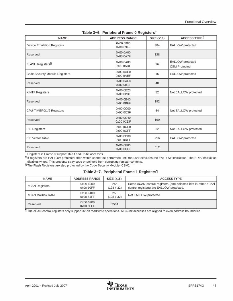
Functional Overview
41April 2001 − Revised July 2007 SPRS174O
Table 3−6. Peripheral Frame 0 Registers † NAME ADDRESS RANGE SIZE (x16) ACCESS TYPE‡
Device Emulation Registers0x00 08800x00 09FF
384 EALLOW protected
Reserved0x00 0A000x00 0A7F
128
FLASH Registers§ 0x00 0A800x00 0ADF
96EALLOW protected
CSM Protected
Code Security Module Registers0x00 0AE00x00 0AEF
16 EALLOW protected
Reserved0x00 0AF00x00 0B1F
48
XINTF Registers0x00 0B200x00 0B3F
32 Not EALLOW protected
Reserved0x00 0B400x00 0BFF
192
CPU-TIMER0/1/2 Registers0x00 0C000x00 0C3F
64 Not EALLOW protected
Reserved0x00 0C400x00 0CDF
160
PIE Registers0x00 0CE00x00 0CFF
32 Not EALLOW protected
PIE Vector Table0x00 0D000x00 0DFF
256 EALLOW protected
Reserved0x00 0E000x00 0FFF
512
† Registers in Frame 0 support 16-bit and 32-bit accesses.‡ If registers are EALLOW protected, then writes cannot be performed until the user executes the EALLOW instruction. The EDIS instruction
disables writes. This prevents stray code or pointers from corrupting register contents.§ The Flash Registers are also protected by the Code Security Module (CSM).
Table 3−7. Peripheral Frame 1 Registers ¶
NAME ADDRESS RANGE SIZE (x16) ACCESS TYPE
eCAN Registers0x00 60000x00 60FF
256(128 x 32)
Some eCAN control registers (and selected bits in other eCANcontrol registers) are EALLOW-protected.
eCAN Mailbox RAM0x00 61000x00 61FF
256(128 x 32)
Not EALLOW-protected
Reserved0x00 62000x00 6FFF
3584
¶ The eCAN control registers only support 32-bit read/write operations. All 32-bit accesses are aligned to even address boundaries.

Functional Overview
42 April 2001 − Revised July 2007SPRS174O
Table 3−8. Peripheral Frame 2 Registers †
NAME ADDRESS RANGE SIZE (x16) ACCESS TYPE
Reserved0x00 70000x00 700F
16
System Control Registers0x00 70100x00 702F
32 EALLOW Protected
Reserved0x00 70300x00 703F
16
SPI-A Registers0x00 70400x00 704F
16 Not EALLOW Protected
SCI-A Registers0x00 70500x00 705F
16 Not EALLOW Protected
Reserved0x00 70600x00 706F
16
External Interrupt Registers0x00 70700x00 707F
16 Not EALLOW Protected
Reserved0x00 70800x00 70BF
64
GPIO Mux Registers0x00 70C00x00 70DF
32 EALLOW Protected
GPIO Data Registers0x00 70E00x00 70FF
32 Not EALLOW Protected
ADC Registers0x00 71000x00 711F
32 Not EALLOW Protected
Reserved0x00 71200x00 73FF
736
EV-A Registers0x00 74000x00 743F
64 Not EALLOW Protected
Reserved0x00 74400x00 74FF
192
EV-B Registers0x00 75000x00 753F
64 Not EALLOW Protected
Reserved0x00 75400x00 774F
528
SCI-B Registers0x00 77500x00 775F
16 Not EALLOW Protected
Reserved0x00 77600x00 77FF
160
McBSP Registers0x00 78000x00 783F
64 Not EALLOW Protected
Reserved0x00 78400x00 7FFF
1984
† Peripheral Frame 2 only allows 16-bit accesses. All 32-bit accesses are ignored (invalid data may be returned or written).
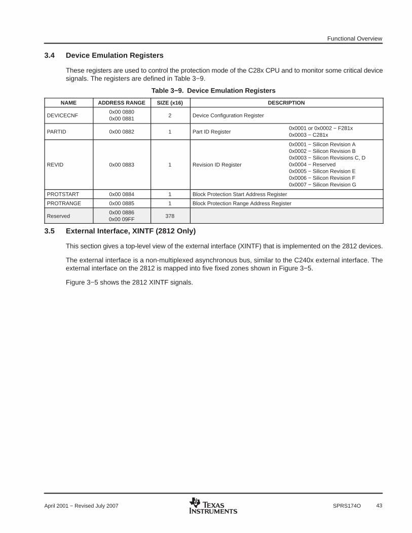
Functional Overview
43April 2001 − Revised July 2007 SPRS174O
3.4 Device Emulation Registers
These registers are used to control the protection mode of the C28x CPU and to monitor some critical devicesignals. The registers are defined in Table 3−9.
Table 3−9. Device Emulation Registers
NAME ADDRESS RANGE SIZE (x16) DESCRIPTION
DEVICECNF0x00 08800x00 0881
2 Device Configuration Register
PARTID 0x00 0882 1 Part ID Register0x0001 or 0x0002 − F281x0x0003 − C281x
REVID 0x00 0883 1 Revision ID Register
0x0001 − Silicon Revision A0x0002 − Silicon Revision B0x0003 − Silicon Revisions C, D0x0004 − Reserved0x0005 − Silicon Revision E0x0006 − Silicon Revision F0x0007 − Silicon Revision G
PROTSTART 0x00 0884 1 Block Protection Start Address Register
PROTRANGE 0x00 0885 1 Block Protection Range Address Register
Reserved0x00 08860x00 09FF
378
3.5 External Interface, XINTF (2812 Only)
This section gives a top-level view of the external interface (XINTF) that is implemented on the 2812 devices.
The external interface is a non-multiplexed asynchronous bus, similar to the C240x external interface. Theexternal interface on the 2812 is mapped into five fixed zones shown in Figure 3−5.
Figure 3−5 shows the 2812 XINTF signals.
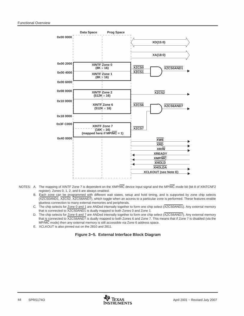
Functional Overview
44 April 2001 − Revised July 2007SPRS174O
XD(15:0)
XA(18:0)
XZCS6
XZCS7
XZCS6AND7
XZCS2
XWE
XR/WXREADYXMP/MCXHOLD
XHOLDAXCLKOUT (see Note E)
XRD
XINTF Zone 0(8K × 16)
XINTF Zone 1(8K × 16)
XINTF Zone 6(512K × 16)
XINTF Zone 7(16K × 16)
(mapped here if MP/MC = 1)
0x40 0000
0x3F C000
0x18 0000
0x10 0000
0x00 6000
0x00 4000
0x00 2000
0x00 0000
Data Space Prog Space
XINTF Zone 2(512K × 16)
0x08 0000
NOTES: A. The mapping of XINTF Zone 7 is dependent on the XMP/MC device input signal and the MP/MC mode bit (bit 8 of XINTCNF2register). Zones 0, 1, 2, and 6 are always enabled.
B. Each zone can be programmed with different wait states, setup and hold timing, and is supported by zone chip selects(XZCS0AND1, XZCS2, XZCS6AND7), which toggle when an access to a particular zone is performed. These features enableglueless connection to many external memories and peripherals.
C. The chip selects for Zone 0 and 1 are ANDed internally together to form one chip select (XZCS0AND1). Any external memorythat is connected to XZCS0AND1 is dually mapped to both Zones 0 and Zone 1.
D. The chip selects for Zone 6 and 7 are ANDed internally together to form one chip select (XZCS6AND7). Any external memorythat is connected to XZCS6AND7 is dually mapped to both Zones 6 and Zone 7. This means that if Zone 7 is disabled (via theMP/MC mode) then any external memory is still accessible via Zone 6 address space.
E. XCLKOUT is also pinned out on the 2810 and 2811.
XZCS0AND1XZCS0XZCS1
Figure 3−5. External Interface Block Diagram

Functional Overview
45April 2001 − Revised July 2007 SPRS174O
The operation and timing of the external interface, can be controlled by the registers listed in Table 3−10.
Table 3−10. XINTF Configuration and Control Register Mappings
NAME ADDRESS SIZE (x16) DESCRIPTION
XTIMING0 0x00 0B20 2 XINTF Timing Register, Zone 0 can access as two 16-bit registers or one 32-bit register
XTIMING1 0x00 0B22 2 XINTF Timing Register, Zone 1 can access as two 16-bit registers or one 32-bit register
XTIMING2 0x00 0B24 2 XINTF Timing Register, Zone 2 can access as two 16-bit registers or one 32-bit register
XTIMING6 0x00 0B2C 2 XINTF Timing Register, Zone 6 can access as two 16-bit registers or one 32-bit register
XTIMING7 0x00 0B2E 2 XINTF Timing Register, Zone 7 can access as two 16-bit registers or one 32-bit register
XINTCNF2 0x00 0B34 2 XINTF Configuration Register can access as two 16-bit registers or one 32-bit register
XBANK 0x00 0B38 1 XINTF Bank Control Register
XREVISION 0x00 0B3A 1 XINTF Revision Register
3.5.1 Timing Registers
XINTF signal timing can be tuned to match specific external device requirements such as setup and hold timesto strobe signals for contention avoidance and maximizing bus efficiency. The XINTF timing parameters canbe configured individually for each zone based on the requirements of the memory or peripheral accessedby that particular zone. This allows the programmer to maximize the efficiency of the bus on a per zone basis.All XINTF timing values are with respect to XTIMCLK, which is equal to or one-half of the SYSCLKOUT rate,as shown in Figure 6−30.
For detailed information on the XINTF timing and configuration register bit fields, see the TMS320x281x DSPExternal Interface (XINTF) Reference Guide (literature number SPRU067).
3.5.2 XREVISION Register
The XREVISION register contains a unique number to identify the particular version of XINTF used in theproduct. For the 2812, this register will be configured as described in Table 3−11.
Table 3−11. XREVISION Register Bit Definitions
BIT(S) NAME TYPE RESET DESCRIPTION
15−0 REVISION R 0x0004Current XINTF Revision. For internal use/reference. Test purposes only. Subject tochange.
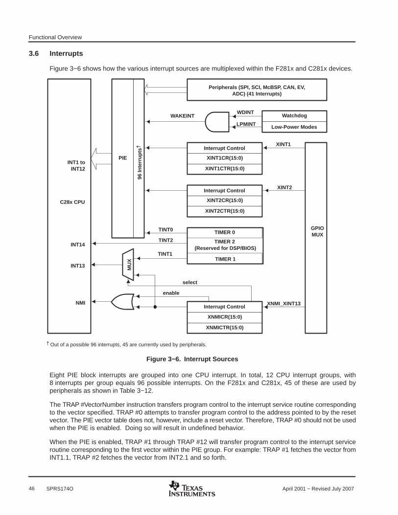
Functional Overview
46 April 2001 − Revised July 2007SPRS174O
3.6 Interrupts
Figure 3−6 shows how the various interrupt sources are multiplexed within the F281x and C281x devices.
C28x CPU
PIE
TIMER 2 (Reserved for DSP/BIOS)
TIMER 0
Watchdog
Peripherals (SPI, SCI, McBSP, CAN, EV,ADC) (41 Interrupts)
96 In
terr
upts
†
TINT0
Interrupt Control
XNMICR(15:0)
XINT1Interrupt Control
XINT1CR(15:0)
XINT2Interrupt Control
XINT2CR(15:0)
GPIOMUX
WDINT
INT1 toINT12
INT13
INT14
NMI
XINT1CTR(15:0)
XINT2CTR(15:0)
XNMICTR(15:0)
TIMER 1
TINT2
Low-Power ModesLPMINT
WAKEINT
XNMI_XINT13
MU
X
TINT1
enable
select
† Out of a possible 96 interrupts, 45 are currently used by peripherals.
Figure 3−6. Interrupt Sources
Eight PIE block interrupts are grouped into one CPU interrupt. In total, 12 CPU interrupt groups, with8 interrupts per group equals 96 possible interrupts. On the F281x and C281x, 45 of these are used byperipherals as shown in Table 3−12.
The TRAP #VectorNumber instruction transfers program control to the interrupt service routine correspondingto the vector specified. TRAP #0 attempts to transfer program control to the address pointed to by the resetvector. The PIE vector table does not, however, include a reset vector. Therefore, TRAP #0 should not be usedwhen the PIE is enabled. Doing so will result in undefined behavior.
When the PIE is enabled, TRAP #1 through TRAP #12 will transfer program control to the interrupt serviceroutine corresponding to the first vector within the PIE group. For example: TRAP #1 fetches the vector fromINT1.1, TRAP #2 fetches the vector from INT2.1 and so forth.
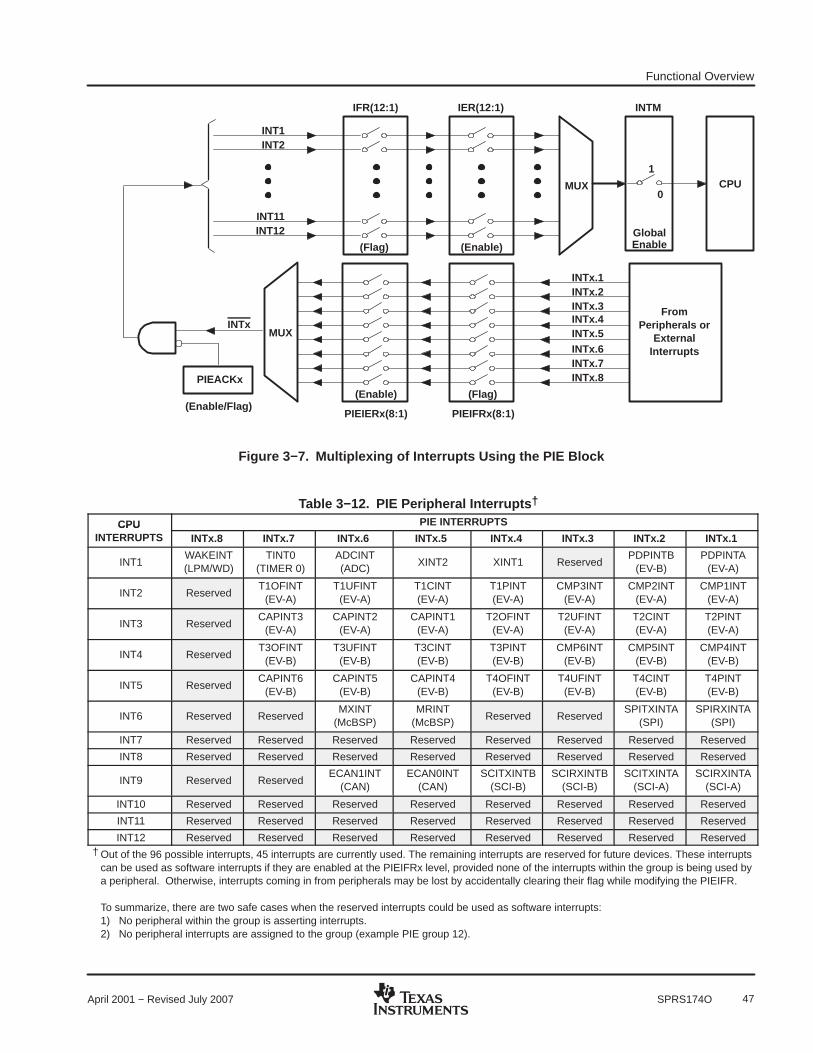
Functional Overview
47April 2001 − Revised July 2007 SPRS174O
INT12
MUX
INT11
INT2INT1
CPU
(Enable)(Flag)
INTx
INTx.8
PIEIERx(8:1) PIEIFRx(8:1)
MUX
INTx.7INTx.6INTx.5INTx.4INTx.3INTx.2INTx.1
FromPeripherals or
ExternalInterrupts
(Enable) (Flag)
IER(12:1)IFR(12:1)
GlobalEnable
INTM
1
0
PIEACKx
(Enable/Flag)
Figure 3−7. Multiplexing of Interrupts Using the PIE Block
Table 3−12. PIE Peripheral Interrupts † CPU PIE INTERRUPTSCPU
INTERRUPTS INTx.8 INTx.7 INTx.6 INTx.5 INTx.4 INTx.3 INTx.2 INTx.1
INT1WAKEINT(LPM/WD)
TINT0(TIMER 0)
ADCINT(ADC)
XINT2 XINT1 ReservedPDPINTB
(EV-B)PDPINTA
(EV-A)
INT2 ReservedT1OFINT
(EV-A)T1UFINT
(EV-A)T1CINT(EV-A)
T1PINT(EV-A)
CMP3INT(EV-A)
CMP2INT(EV-A)
CMP1INT(EV-A)
INT3 ReservedCAPINT3
(EV-A)CAPINT2
(EV-A)CAPINT1
(EV-A)T2OFINT
(EV-A)T2UFINT
(EV-A)T2CINT(EV-A)
T2PINT(EV-A)
INT4 ReservedT3OFINT
(EV-B)T3UFINT
(EV-B)T3CINT(EV-B)
T3PINT(EV-B)
CMP6INT(EV-B)
CMP5INT(EV-B)
CMP4INT(EV-B)
INT5 ReservedCAPINT6
(EV-B)CAPINT5
(EV-B)CAPINT4
(EV-B)T4OFINT
(EV-B)T4UFINT
(EV-B)T4CINT(EV-B)
T4PINT(EV-B)
INT6 Reserved ReservedMXINT
(McBSP)MRINT
(McBSP)Reserved Reserved
SPITXINTA(SPI)
SPIRXINTA(SPI)
INT7 Reserved Reserved Reserved Reserved Reserved Reserved Reserved Reserved
INT8 Reserved Reserved Reserved Reserved Reserved Reserved Reserved Reserved
INT9 Reserved ReservedECAN1INT
(CAN)ECAN0INT
(CAN)SCITXINTB
(SCI-B)SCIRXINTB
(SCI-B)SCITXINTA
(SCI-A)SCIRXINTA
(SCI-A)
INT10 Reserved Reserved Reserved Reserved Reserved Reserved Reserved Reserved
INT11 Reserved Reserved Reserved Reserved Reserved Reserved Reserved Reserved
INT12 Reserved Reserved Reserved Reserved Reserved Reserved Reserved Reserved† Out of the 96 possible interrupts, 45 interrupts are currently used. The remaining interrupts are reserved for future devices. These interrupts
can be used as software interrupts if they are enabled at the PIEIFRx level, provided none of the interrupts within the group is being used bya peripheral. Otherwise, interrupts coming in from peripherals may be lost by accidentally clearing their flag while modifying the PIEIFR.
To summarize, there are two safe cases when the reserved interrupts could be used as software interrupts:1) No peripheral within the group is asserting interrupts. 2) No peripheral interrupts are assigned to the group (example PIE group 12).
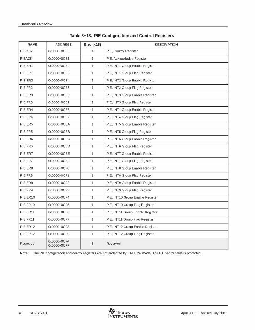
Functional Overview
48 April 2001 − Revised July 2007SPRS174O
Table 3−13. PIE Configuration and Control Registers
NAME ADDRESS Size (x16) DESCRIPTION
PIECTRL 0x0000−0CE0 1 PIE, Control Register
PIEACK 0x0000−0CE1 1 PIE, Acknowledge Register
PIEIER1 0x0000−0CE2 1 PIE, INT1 Group Enable Register
PIEIFR1 0x0000−0CE3 1 PIE, INT1 Group Flag Register
PIEIER2 0x0000−0CE4 1 PIE, INT2 Group Enable Register
PIEIFR2 0x0000−0CE5 1 PIE, INT2 Group Flag Register
PIEIER3 0x0000−0CE6 1 PIE, INT3 Group Enable Register
PIEIFR3 0x0000−0CE7 1 PIE, INT3 Group Flag Register
PIEIER4 0x0000−0CE8 1 PIE, INT4 Group Enable Register
PIEIFR4 0x0000−0CE9 1 PIE, INT4 Group Flag Register
PIEIER5 0x0000−0CEA 1 PIE, INT5 Group Enable Register
PIEIFR5 0x0000−0CEB 1 PIE, INT5 Group Flag Register
PIEIER6 0x0000−0CEC 1 PIE, INT6 Group Enable Register
PIEIFR6 0x0000−0CED 1 PIE, INT6 Group Flag Register
PIEIER7 0x0000−0CEE 1 PIE, INT7 Group Enable Register
PIEIFR7 0x0000−0CEF 1 PIE, INT7 Group Flag Register
PIEIER8 0x0000−0CF0 1 PIE, INT8 Group Enable Register
PIEIFR8 0x0000−0CF1 1 PIE, INT8 Group Flag Register
PIEIER9 0x0000−0CF2 1 PIE, INT9 Group Enable Register
PIEIFR9 0x0000−0CF3 1 PIE, INT9 Group Flag Register
PIEIER10 0x0000−0CF4 1 PIE, INT10 Group Enable Register
PIEIFR10 0x0000−0CF5 1 PIE, INT10 Group Flag Register
PIEIER11 0x0000−0CF6 1 PIE, INT11 Group Enable Register
PIEIFR11 0x0000−0CF7 1 PIE, INT11 Group Flag Register
PIEIER12 0x0000−0CF8 1 PIE, INT12 Group Enable Register
PIEIFR12 0x0000−0CF9 1 PIE, INT12 Group Flag Register
Reserved0x0000−0CFA0x0000−0CFF
6 Reserved
Note: The PIE configuration and control registers are not protected by EALLOW mode. The PIE vector table is protected.
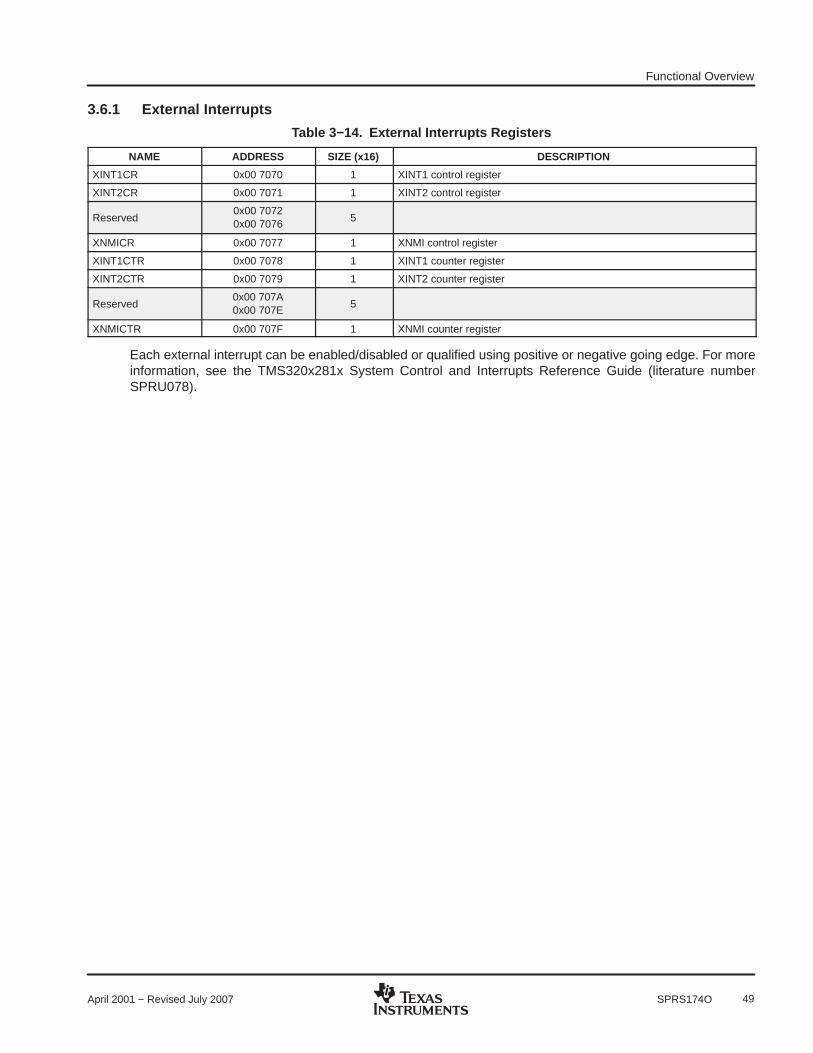
Functional Overview
49April 2001 − Revised July 2007 SPRS174O
3.6.1 External Interrupts
Table 3−14. External Interrupts Registers
NAME ADDRESS SIZE (x16) DESCRIPTION
XINT1CR 0x00 7070 1 XINT1 control register
XINT2CR 0x00 7071 1 XINT2 control register
Reserved0x00 70720x00 7076
5
XNMICR 0x00 7077 1 XNMI control register
XINT1CTR 0x00 7078 1 XINT1 counter register
XINT2CTR 0x00 7079 1 XINT2 counter register
Reserved0x00 707A0x00 707E
5
XNMICTR 0x00 707F 1 XNMI counter register
Each external interrupt can be enabled/disabled or qualified using positive or negative going edge. For moreinformation, see the TMS320x281x System Control and Interrupts Reference Guide (literature numberSPRU078).

Functional Overview
50 April 2001 − Revised July 2007SPRS174O
3.7 System Control
This section describes the F281x and C281x oscillator, PLL and clocking mechanisms, the watchdog functionand the low power modes. Figure 3−8 shows the various clock and reset domains in the F281x and C281xdevices that will be discussed.
HSPCLK
PLL
X1/XCLKIN
X2
PowerModesControl
WatchdogBlock
C28xCPU
Per
iphe
ral B
us Low-Speed PeripheralsSCI-A/B, SPI, McBSP
PeripheralRegisters
High-Speed Peripherals EV-A/B
High-Speed Prescaler
Low-Speed Prescaler
Clock Enables
GPIOMUX
SystemControl
Registers
PeripheralRegisters
XF_XPLLDIS
ADCRegisters
12-Bit ADC 16 ADC Inputs
HSPCLK
LSPCLK
I/O
I/O
Peripheral Reset
SYSCLKOUTXRS
Reset
GPIOs
eCANPeripheralRegisters I/O
OSC
CLKIN(A)
NOTE A: CLKIN is the clock input to the CPU. SYSCLKOUT is the output clock of the CPU. They are of the same frequency.
Figure 3−8. Clock and Reset Domains
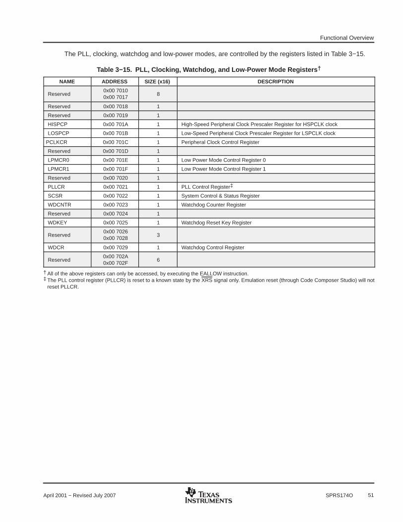
Functional Overview
51April 2001 − Revised July 2007 SPRS174O
The PLL, clocking, watchdog and low-power modes, are controlled by the registers listed in Table 3−15.
Table 3−15. PLL, Clocking, Watchdog, and Low-Power Mode Registers †
NAME ADDRESS SIZE (x16) DESCRIPTION
Reserved0x00 70100x00 7017
8
Reserved 0x00 7018 1
Reserved 0x00 7019 1
HISPCP 0x00 701A 1 High-Speed Peripheral Clock Prescaler Register for HSPCLK clock
LOSPCP 0x00 701B 1 Low-Speed Peripheral Clock Prescaler Register for LSPCLK clock
PCLKCR 0x00 701C 1 Peripheral Clock Control Register
Reserved 0x00 701D 1
LPMCR0 0x00 701E 1 Low Power Mode Control Register 0
LPMCR1 0x00 701F 1 Low Power Mode Control Register 1
Reserved 0x00 7020 1
PLLCR 0x00 7021 1 PLL Control Register‡
SCSR 0x00 7022 1 System Control & Status Register
WDCNTR 0x00 7023 1 Watchdog Counter Register
Reserved 0x00 7024 1
WDKEY 0x00 7025 1 Watchdog Reset Key Register
Reserved0x00 70260x00 7028
3
WDCR 0x00 7029 1 Watchdog Control Register
Reserved0x00 702A0x00 702F
6
† All of the above registers can only be accessed, by executing the EALLOW instruction.‡ The PLL control register (PLLCR) is reset to a known state by the XRS signal only. Emulation reset (through Code Composer Studio) will not
reset PLLCR.
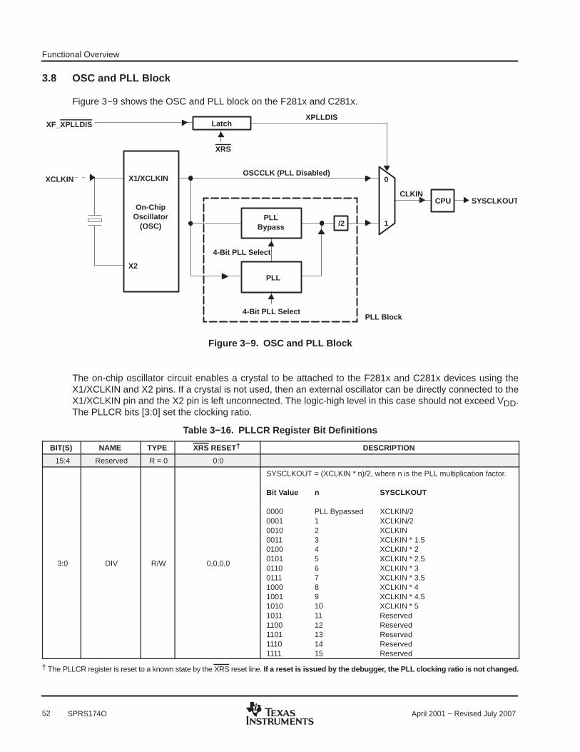
Functional Overview
52 April 2001 − Revised July 2007SPRS174O
3.8 OSC and PLL Block
Figure 3−9 shows the OSC and PLL block on the F281x and C281x.
X2
X1/XCLKIN
On-ChipOscillator
(OSC)PLL
Bypass /2
XF_XPLLDIS
OSCCLK (PLL Disabled)
LatchXPLLDIS
XRS
PLL
4-Bit PLL Select
SYSCLKOUT
1
0
CLKINCPU
4-Bit PLL Select
XCLKIN
PLL Block
Figure 3−9. OSC and PLL Block
The on-chip oscillator circuit enables a crystal to be attached to the F281x and C281x devices using theX1/XCLKIN and X2 pins. If a crystal is not used, then an external oscillator can be directly connected to theX1/XCLKIN pin and the X2 pin is left unconnected. The logic-high level in this case should not exceed VDD.The PLLCR bits [3:0] set the clocking ratio.
Table 3−16. PLLCR Register Bit Definitions
BIT(S) NAME TYPE XRS RESET† DESCRIPTION
15:4 Reserved R = 0 0:0
3:0 DIV R/W 0,0,0,0
SYSCLKOUT = (XCLKIN * n)/2, where n is the PLL multiplication factor.
Bit Value n SYSCLKOUT
0000 PLL Bypassed XCLKIN/20001 1 XCLKIN/20010 2 XCLKIN0011 3 XCLKIN * 1.50100 4 XCLKIN * 20101 5 XCLKIN * 2.50110 6 XCLKIN * 30111 7 XCLKIN * 3.51000 8 XCLKIN * 41001 9 XCLKIN * 4.51010 10 XCLKIN * 51011 11 Reserved1100 12 Reserved1101 13 Reserved1110 14 Reserved1111 15 Reserved
† The PLLCR register is reset to a known state by the XRS reset line. If a reset is issued by the debugger, the PLL clocking ratio is not changed.

Functional Overview
53April 2001 − Revised July 2007 SPRS174O
3.8.1 Loss of Input Clock
In PLL enabled mode, if the input clock XCLKIN or the oscillator clock is removed or absent, the PLL will stillissue a “limp-mode” clock. The limp-mode clock will continue to clock the CPU and peripherals at a typicalfrequency of 1−4 MHz. The PLLCR register should have been written to with a non-zero value for this featureto work.
Normally, when the input clocks are present, the watchdog counter will decrement to initiate a watchdog resetor WDINT interrupt. However, when the external input clock fails, the watchdog counter will stop decrementing(i.e., the watchdog counter does not change with the limp-mode clock). This condition could be used by theapplication firmware to detect the input clock failure and initiate necessary shut-down procedure for thesystem.
NOTE:Applications in which the correct CPU operating frequency is absolutely critical mustimplement a mechanism by which the DSP will be held in reset, should the input clocks everfail. For example, an R-C circuit may be used to trigger the XRS pin of the DSP, should thecapacitor ever get fully charged. An I/O pin may be used to discharge the capacitor on aperiodic basis to prevent it from getting fully charged. Such a circuit would also help indetecting failure of the VDD3VFL rail.
3.9 PLL-Based Clock Module
The F281x and C281x have an on-chip, PLL-based clock module. This module provides all the necessaryclocking signals for the device, as well as control for low-power mode entry. The PLL has a 4-bit ratio controlto select different CPU clock rates. The watchdog module should be disabled before writing to the PLLCRregister. It can be re-enabled (if need be) after the PLL module has stabilized, which takes 131072 XCLKINcycles.
The PLL-based clock module provides two modes of operation:
• Crystal-operationThis mode allows the use of an external crystal/resonator to provide the time base to the device.
• External clock source operationThis mode allows the internal oscillator to be bypassed. The device clocks are generated from an externalclock source input on the X1/XCLKIN pin.
External Clock Signal (Toggling 0−V DD)
CL1(see Note A)
X2X1/XCLKIN X1/XCLKIN X2
CrystalCL2(see Note A)
(a) (b)
NC
NOTE A: TI recommends that customers have the resonator/crystal vendor characterize the operation of their device with the DSP chip. Theresonator/crystal vendor has the equipment and expertise to tune the tank circuit. The vendor can also advise the customer regardingthe proper tank component values that will ensure start-up and stability over the entire operating range.
Figure 3−10. Recommended Crystal /Clock Connection

Functional Overview
54 April 2001 − Revised July 2007SPRS174O
Table 3−17. Possible PLL Configuration Modes
PLL MODE REMARKS SYSCLKOUT
PLL DisabledInvoked by tying XPLLDIS pin low upon reset. PLL block is completelydisabled. Clock input to the CPU (CLKIN) is directly derived from the clocksignal present at the X1/XCLKIN pin.
XCLKIN
PLL BypassedDefault PLL configuration upon power-up, if PLL is not disabled. The PLLitself is bypassed. However, the /2 module in the PLL block divides the clockinput at the X1/XCLKIN pin by two before feeding it to the CPU.
XCLKIN/2
PLL EnabledAchieved by writing a non-zero value “n” into PLLCR register. The /2 modulein the PLL block now divides the output of the PLL by two before feeding it tothe CPU.
(XCLKIN * n) / 2
3.10 External Reference Oscillator Clock Option
The typical specifications for the external quartz crystal for a frequency of 30 MHz are listed below:
• Fundamental mode, parallel resonant
• CL (load capacitance) = 12 pF
• CL1 = CL2 = 24 pF
• Cshunt = 6 pF
• ESR range = 25 to 40 Ω
3.11 Watchdog Block
The watchdog block on the F281x and C281x is identical to the one used on the 240x devices. The watchdogmodule generates an output pulse, 512 oscillator clocks wide (OSCCLK), whenever the 8-bit watchdog upcounter has reached its maximum value. To prevent this, the user disables the counter or the software mustperiodically write a 0x55 + 0xAA sequence into the watchdog key register which will reset the watchdogcounter. Figure 3−11 shows the various functional blocks within the watchdog module.
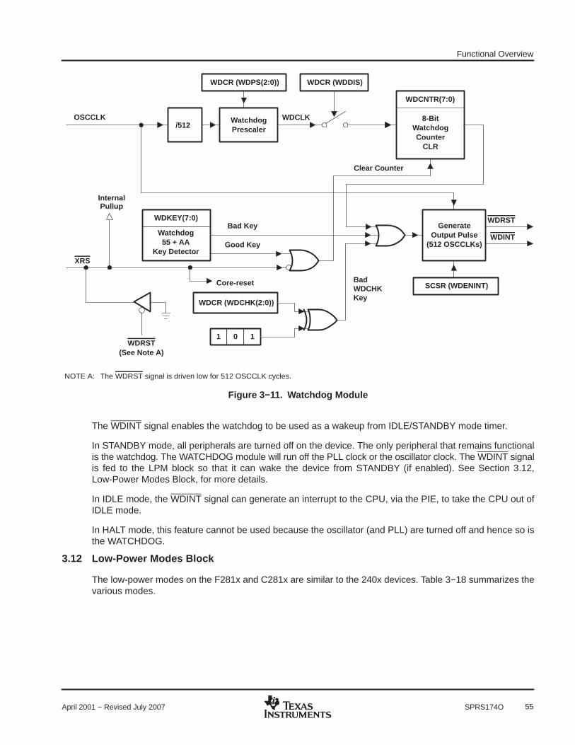
Functional Overview
55April 2001 − Revised July 2007 SPRS174O
/512OSCCLK
WDCR (WDPS(2:0))
WDCLK
WDCNTR(7:0)
WDKEY(7:0)Bad Key
Good Key
1 0 1
WDCR (WDCHK(2:0))
BadWDCHKKey
WDCR (WDDIS)
Clear Counter
SCSR (WDENINT)
WatchdogPrescaler
GenerateOutput Pulse
(512 OSCCLKs)
8-BitWatchdogCounter
CLR
WDRST
WDINTWatchdog55 + AA
Key DetectorXRS
Core-reset
NOTE A: The WDRST signal is driven low for 512 OSCCLK cycles.
WDRST(See Note A)
InternalPullup
Figure 3−11. Watchdog Module
The WDINT signal enables the watchdog to be used as a wakeup from IDLE/STANDBY mode timer.
In STANDBY mode, all peripherals are turned off on the device. The only peripheral that remains functionalis the watchdog. The WATCHDOG module will run off the PLL clock or the oscillator clock. The WDINT signalis fed to the LPM block so that it can wake the device from STANDBY (if enabled). See Section 3.12,Low-Power Modes Block, for more details.
In IDLE mode, the WDINT signal can generate an interrupt to the CPU, via the PIE, to take the CPU out ofIDLE mode.
In HALT mode, this feature cannot be used because the oscillator (and PLL) are turned off and hence so isthe WATCHDOG.
3.12 Low-Power Modes Block
The low-power modes on the F281x and C281x are similar to the 240x devices. Table 3−18 summarizes thevarious modes.
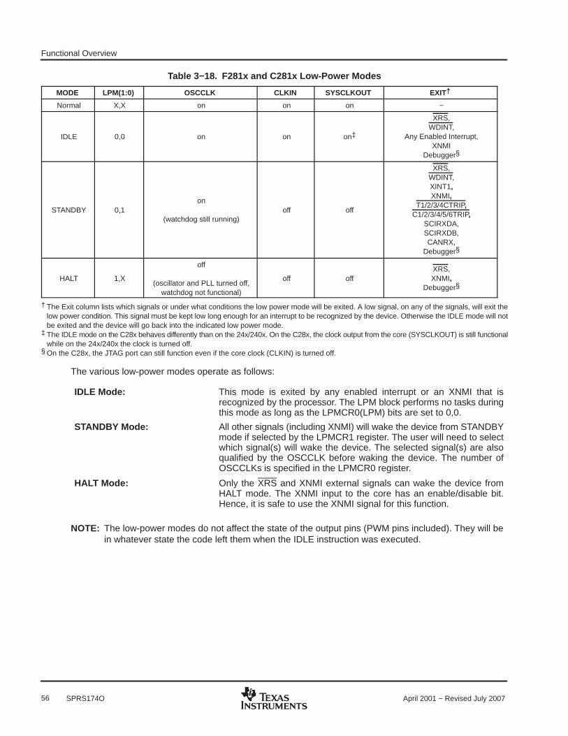
Functional Overview
56 April 2001 − Revised July 2007SPRS174O
Table 3−18. F281x and C281x Low-Power Modes
MODE LPM(1:0) OSCCLK CLKIN SYSCLKOUT EXIT†
Normal X,X on on on −
IDLE 0,0 on on on‡
XRS,WDINT,
Any Enabled Interrupt,XNMI
Debugger§
STANDBY 0,1on
(watchdog still running)off off
XRS,WDINT,XINT1,XNMI,
T1/2/3/4CTRIP,C1/2/3/4/5/6TRIP,
SCIRXDA,SCIRXDB,CANRX,
Debugger§
HALT 1,X
off
(oscillator and PLL turned off,watchdog not functional)
off offXRS,XNMI,
Debugger§
† The Exit column lists which signals or under what conditions the low power mode will be exited. A low signal, on any of the signals, will exit thelow power condition. This signal must be kept low long enough for an interrupt to be recognized by the device. Otherwise the IDLE mode will notbe exited and the device will go back into the indicated low power mode.
‡ The IDLE mode on the C28x behaves differently than on the 24x/240x. On the C28x, the clock output from the core (SYSCLKOUT) is still functionalwhile on the 24x/240x the clock is turned off.
§ On the C28x, the JTAG port can still function even if the core clock (CLKIN) is turned off.
The various low-power modes operate as follows:
IDLE Mode: This mode is exited by any enabled interrupt or an XNMI that isrecognized by the processor. The LPM block performs no tasks duringthis mode as long as the LPMCR0(LPM) bits are set to 0,0.
STANDBY Mode: All other signals (including XNMI) will wake the device from STANDBYmode if selected by the LPMCR1 register. The user will need to selectwhich signal(s) will wake the device. The selected signal(s) are alsoqualified by the OSCCLK before waking the device. The number ofOSCCLKs is specified in the LPMCR0 register.
HALT Mode: Only the XRS and XNMI external signals can wake the device fromHALT mode. The XNMI input to the core has an enable/disable bit.Hence, it is safe to use the XNMI signal for this function.
NOTE: The low-power modes do not affect the state of the output pins (PWM pins included). They will bein whatever state the code left them when the IDLE instruction was executed.
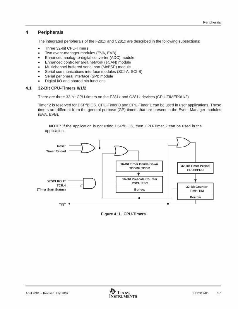
Peripherals
57April 2001 − Revised July 2007 SPRS174O
4 Peripherals
The integrated peripherals of the F281x and C281x are described in the following subsections:
• Three 32-bit CPU-Timers• Two event-manager modules (EVA, EVB)• Enhanced analog-to-digital converter (ADC) module• Enhanced controller area network (eCAN) module• Multichannel buffered serial port (McBSP) module• Serial communications interface modules (SCI-A, SCI-B)• Serial peripheral interface (SPI) module• Digital I/O and shared pin functions
4.1 32-Bit CPU-Timers 0/1/2
There are three 32-bit CPU-timers on the F281x and C281x devices (CPU-TIMER0/1/2).
Timer 2 is reserved for DSP/BIOS. CPU-Timer 0 and CPU-Timer 1 can be used in user applications. Thesetimers are different from the general-purpose (GP) timers that are present in the Event Manager modules(EVA, EVB).
NOTE: If the application is not using DSP/BIOS, then CPU-Timer 2 can be used in theapplication.
Borrow
Reset
Timer Reload
SYSCLKOUTTCR.4
(Timer Start Status)
TINT
16-Bit Timer Divide-Down TDDRH:TDDR
32-Bit Timer PeriodPRDH:PRD
32-Bit CounterTIMH:TIM
16-Bit Prescale CounterPSCH:PSC
Borrow
Figure 4−1. CPU-Timers

Peripherals
58 April 2001 − Revised July 2007SPRS174O
In the F281x and C281x devices, the timer interrupt signals (TINT0, TINT1, TINT2) are connected as shownin Figure 4−2.
INT1to
INT12
INT14
28xCPU
TINT2
TINT0PIE CPU-TIMER 0
CPU-TIMER 2 (Reserved for DSP/BIOS)
INT13TINT1
CPU-TIMER 1
XINT13
Figure 4−2. CPU-Timer Interrupts Signals and Output Signal (See Notes A and B)
The general operation of the timer is as follows: The 32-bit counter register “TIMH:TIM” is loaded with the valuein the period register “PRDH:PRD”. The counter register decrements at the SYSCLKOUT rate of the C28x.When the counter reaches 0, a timer interrupt output signal generates an interrupt pulse. The registers listedin Table 4−1 are used to configure the timers. For more information, see the TMS320x281x System Controland Interrupts Reference Guide (literature number SPRU078).
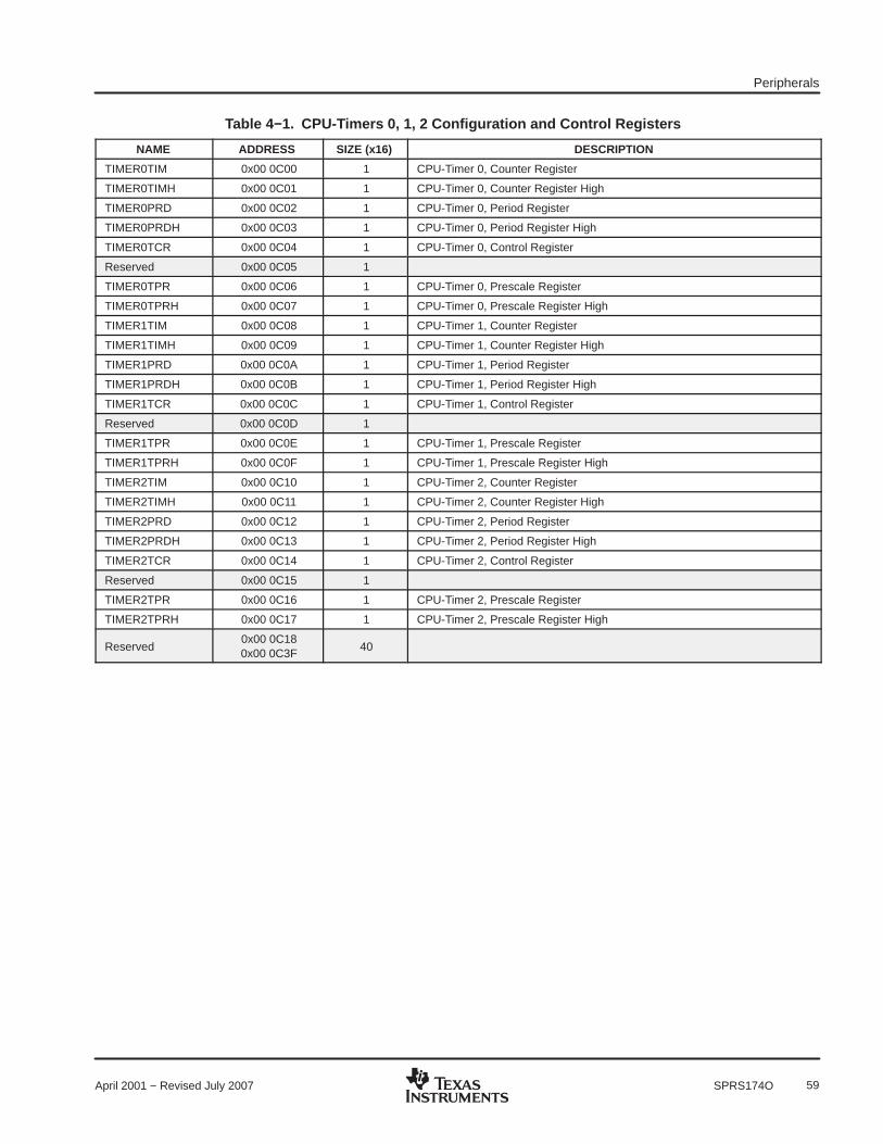
Peripherals
59April 2001 − Revised July 2007 SPRS174O
Table 4−1. CPU-Timers 0, 1, 2 Configuration and Control Registers
NAME ADDRESS SIZE (x16) DESCRIPTION
TIMER0TIM 0x00 0C00 1 CPU-Timer 0, Counter Register
TIMER0TIMH 0x00 0C01 1 CPU-Timer 0, Counter Register High
TIMER0PRD 0x00 0C02 1 CPU-Timer 0, Period Register
TIMER0PRDH 0x00 0C03 1 CPU-Timer 0, Period Register High
TIMER0TCR 0x00 0C04 1 CPU-Timer 0, Control Register
Reserved 0x00 0C05 1
TIMER0TPR 0x00 0C06 1 CPU-Timer 0, Prescale Register
TIMER0TPRH 0x00 0C07 1 CPU-Timer 0, Prescale Register High
TIMER1TIM 0x00 0C08 1 CPU-Timer 1, Counter Register
TIMER1TIMH 0x00 0C09 1 CPU-Timer 1, Counter Register High
TIMER1PRD 0x00 0C0A 1 CPU-Timer 1, Period Register
TIMER1PRDH 0x00 0C0B 1 CPU-Timer 1, Period Register High
TIMER1TCR 0x00 0C0C 1 CPU-Timer 1, Control Register
Reserved 0x00 0C0D 1
TIMER1TPR 0x00 0C0E 1 CPU-Timer 1, Prescale Register
TIMER1TPRH 0x00 0C0F 1 CPU-Timer 1, Prescale Register High
TIMER2TIM 0x00 0C10 1 CPU-Timer 2, Counter Register
TIMER2TIMH 0x00 0C11 1 CPU-Timer 2, Counter Register High
TIMER2PRD 0x00 0C12 1 CPU-Timer 2, Period Register
TIMER2PRDH 0x00 0C13 1 CPU-Timer 2, Period Register High
TIMER2TCR 0x00 0C14 1 CPU-Timer 2, Control Register
Reserved 0x00 0C15 1
TIMER2TPR 0x00 0C16 1 CPU-Timer 2, Prescale Register
TIMER2TPRH 0x00 0C17 1 CPU-Timer 2, Prescale Register High
Reserved0x00 0C180x00 0C3F
40
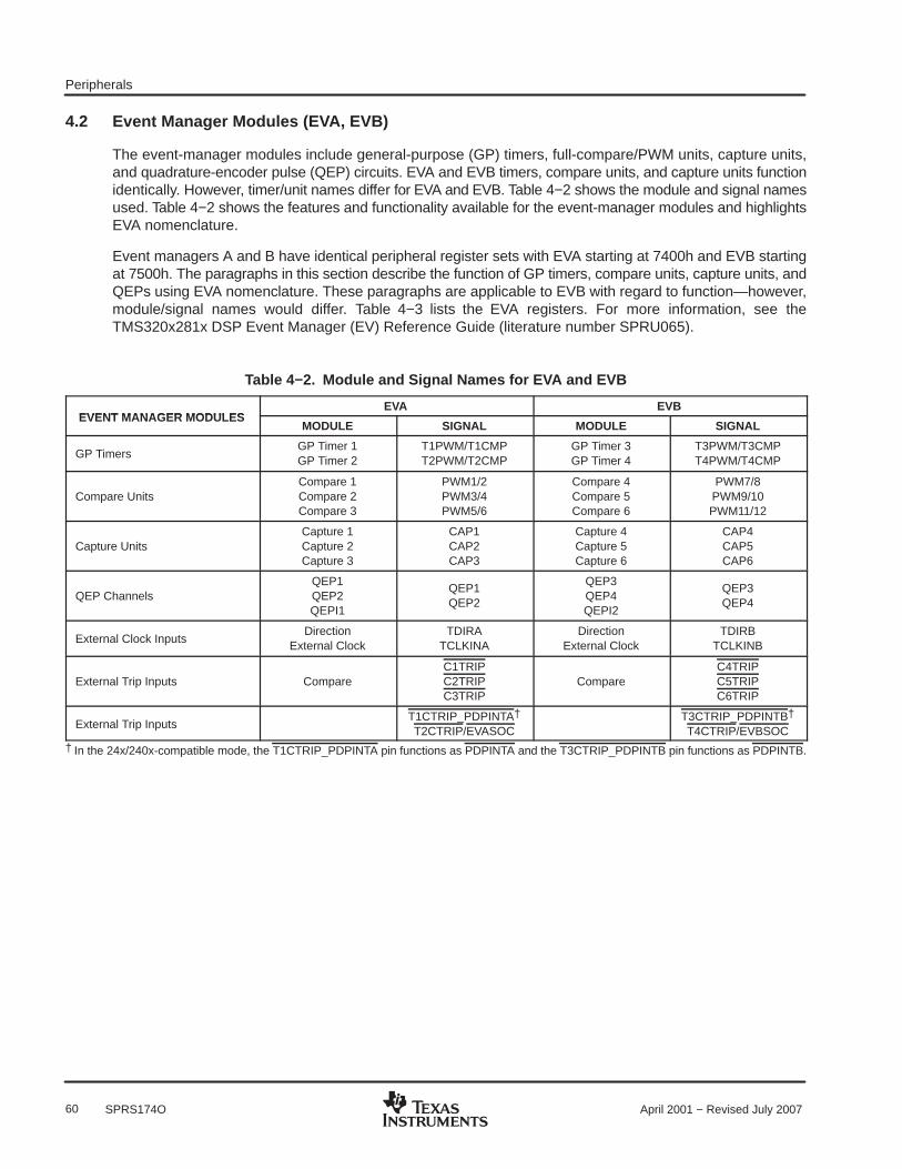
Peripherals
60 April 2001 − Revised July 2007SPRS174O
4.2 Event Manager Modules (EVA, EVB)
The event-manager modules include general-purpose (GP) timers, full-compare/PWM units, capture units,and quadrature-encoder pulse (QEP) circuits. EVA and EVB timers, compare units, and capture units functionidentically. However, timer/unit names differ for EVA and EVB. Table 4−2 shows the module and signal namesused. Table 4−2 shows the features and functionality available for the event-manager modules and highlightsEVA nomenclature.
Event managers A and B have identical peripheral register sets with EVA starting at 7400h and EVB startingat 7500h. The paragraphs in this section describe the function of GP timers, compare units, capture units, andQEPs using EVA nomenclature. These paragraphs are applicable to EVB with regard to function—however,module/signal names would differ. Table 4−3 lists the EVA registers. For more information, see theTMS320x281x DSP Event Manager (EV) Reference Guide (literature number SPRU065).
Table 4−2. Module and Signal Names for EVA and EVB
EVENT MANAGER MODULESEVA EVB
EVENT MANAGER MODULESMODULE SIGNAL MODULE SIGNAL
GP TimersGP Timer 1GP Timer 2
T1PWM/T1CMPT2PWM/T2CMP
GP Timer 3GP Timer 4
T3PWM/T3CMPT4PWM/T4CMP
Compare UnitsCompare 1Compare 2Compare 3
PWM1/2PWM3/4PWM5/6
Compare 4Compare 5Compare 6
PWM7/8PWM9/10PWM11/12
Capture UnitsCapture 1Capture 2Capture 3
CAP1CAP2CAP3
Capture 4Capture 5Capture 6
CAP4CAP5CAP6
QEP ChannelsQEP1QEP2QEPI1
QEP1QEP2
QEP3QEP4QEPI2
QEP3QEP4
External Clock InputsDirection
External ClockTDIRA
TCLKINADirection
External ClockTDIRB
TCLKINB
External Trip Inputs CompareC1TRIPC2TRIPC3TRIP
CompareC4TRIPC5TRIPC6TRIP
External Trip InputsT1CTRIP_PDPINTA†
T2CTRIP/EVASOCT3CTRIP_PDPINTB†
T4CTRIP/EVBSOC† In the 24x/240x-compatible mode, the T1CTRIP_PDPINTA pin functions as PDPINTA and the T3CTRIP_PDPINTB pin functions as PDPINTB.

Peripherals
61April 2001 − Revised July 2007 SPRS174O
Table 4−3. EVA Registers †
NAME ADDRESSSIZE(x16) DESCRIPTION
GPTCONA 0x00 7400 1 GP Timer Control Register A
T1CNT 0x00 7401 1 GP Timer 1 Counter Register
T1CMPR 0x00 7402 1 GP Timer 1 Compare Register
T1PR 0x00 7403 1 GP Timer 1 Period Register
T1CON 0x00 7404 1 GP Timer 1 Control Register
T2CNT 0x00 7405 1 GP Timer 2 Counter Register
T2CMPR 0x00 7406 1 GP Timer 2 Compare Register
T2PR 0x00 7407 1 GP Timer 2 Period Register
T2CON 0x00 7408 1 GP Timer 2 Control Register
EXTCONA‡ 0x00 7409 1 GP Extension Control Register A
COMCONA 0x00 7411 1 Compare Control Register A
ACTRA 0x00 7413 1 Compare Action Control Register A
DBTCONA 0x00 7415 1 Dead-Band Timer Control Register A
CMPR1 0x00 7417 1 Compare Register 1
CMPR2 0x00 7418 1 Compare Register 2
CMPR3 0x00 7419 1 Compare Register 3
CAPCONA 0x00 7420 1 Capture Control Register A
CAPFIFOA 0x00 7422 1 Capture FIFO Status Register A
CAP1FIFO 0x00 7423 1 Two-Level Deep Capture FIFO Stack 1
CAP2FIFO 0x00 7424 1 Two-Level Deep Capture FIFO Stack 2
CAP3FIFO 0x00 7425 1 Two-Level Deep Capture FIFO Stack 3
CAP1FBOT 0x00 7427 1 Bottom Register Of Capture FIFO Stack 1
CAP2FBOT 0x00 7428 1 Bottom Register Of Capture FIFO Stack 2
CAP3FBOT 0x00 7429 1 Bottom Register Of Capture FIFO Stack 3
EVAIMRA 0x00 742C 1 Interrupt Mask Register A
EVAIMRB 0x00 742D 1 Interrupt Mask Register B
EVAIMRC 0x00 742E 1 Interrupt Mask Register C
EVAIFRA 0x00 742F 1 Interrupt Flag Register A
EVAIFRB 0x00 7430 1 Interrupt Flag Register B
EVAIFRC 0x00 7431 1 Interrupt Flag Register C
† The EV-B register set is identical except the address range is from 0x00−7500 to 0x00−753F. The above registers are mapped to Zone 2. Thisspace allows only 16-bit accesses. 32-bit accesses produce undefined results.
‡ New register compared to 24x/240x
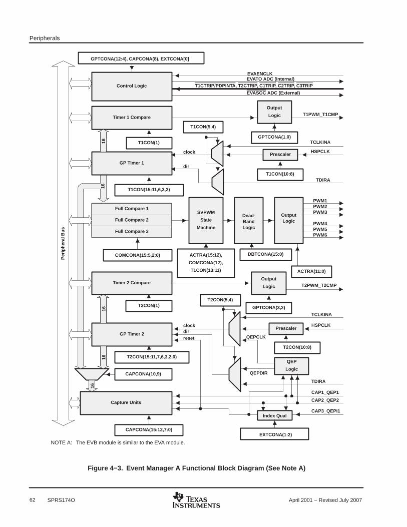
Peripherals
62 April 2001 − Revised July 2007SPRS174O
GPTCONA(12:4), CAPCONA(8), EXTCONA[0]
EVATO ADC (Internal)
Timer 1 Compare
Output
Logic T1PWM_T1CMP
GPTCONA(1,0)T1CON(1)
GP Timer 1
TCLKINA
PrescalerHSPCLK
T1CON(10:8)
T1CON(5,4)
clock
Full Compare 1
Full Compare 2
Full Compare 3
SVPWM
State
Machine
Dead-BandLogic
OutputLogic
PWM1PWM2PWM3
PWM4PWM5PWM6
T1CON(15:11,6,3,2)
TDIRA
dir
Timer 2 Compare
GP Timer 2
16
Capture Units
COMCONA(15:5,2:0)
T1CTRIP/PDPINTA, T2CTRIP, C1TRIP, C2TRIP, C3TRIP
Output
Logic T2PWM_T2CMP
GPTCONA(3,2)T2CON(1)
T2CON(15:11,7,6,3,2,0)
ACTRA(15:12),
COMCONA(12),
T1CON(13:11)
CAPCONA(10,9)
16
DBTCONA(15:0)
ACTRA(11:0)
TCLKINA
PrescalerHSPCLK
T2CON(10:8)
T2CON(5,4)
clockdir
CAPCONA(15:12,7:0)
CAP1_QEP1
CAP2_QEP2
CAP3_QEPI1
QEP
Logic
QEPCLK
QEPDIR
1616
reset
EVAENCLK
Control Logic
Per
iphe
ral B
us
TDIRA
Index Qual
EXTCONA(1:2)
NOTE A: The EVB module is similar to the EVA module.
16
EVASOC ADC (External)
Figure 4−3. Event Manager A Functional Block Diagram (See Note A)

Peripherals
63April 2001 − Revised July 2007 SPRS174O
4.2.1 General-Purpose (GP) Timers
There are two GP timers. The GP timer x (x = 1 or 2 for EVA; x = 3 or 4 for EVB) includes:
• A 16-bit timer, up-/down-counter, TxCNT, for reads or writes
• A 16-bit timer-compare register, TxCMPR (double-buffered with shadow register), for reads or writes
• A 16-bit timer-period register, TxPR (double-buffered with shadow register), for reads or writes
• A 16-bit timer-control register,TxCON, for reads or writes
• Selectable internal or external input clocks
• A programmable prescaler for internal or external clock inputs
• Control and interrupt logic, for four maskable interrupts: underflow, overflow, timer compare, and periodinterrupts
• A selectable direction input pin (TDIRx) (to count up or down when directional up-/down-count mode isselected)
The GP timers can be operated independently or synchronized with each other. The compare registerassociated with each GP timer can be used for compare function and PWM-waveform generation. There arethree continuous modes of operations for each GP timer in up- or up/down-counting operations. Internal orexternal input clocks with programmable prescaler are used for each GP timer. GP timers also provide thetime base for the other event-manager submodules: GP timer 1 for all the compares and PWM circuits, GPtimer 2/1 for the capture units and the quadrature-pulse counting operations. Double-buffering of the periodand compare registers allows programmable change of the timer (PWM) period and the compare/PWM pulsewidth as needed.
4.2.2 Full-Compare Units
There are three full-compare units on each event manager. These compare units use GP timer1 as the timebase and generate six outputs for compare and PWM-waveform generation using programmable deadbandcircuit. The state of each of the six outputs is configured independently. The compare registers of the compareunits are double-buffered, allowing programmable change of the compare/PWM pulse widths as needed.
4.2.3 Programmable Deadband Generator
Deadband generation can be enabled/disabled for each compare unit output individually. Thedeadband-generator circuit produces two outputs (with or without deadband zone) for each compare unitoutput signal. The output states of the deadband generator are configurable and changeable as needed byway of the double-buffered ACTRx register.
4.2.4 PWM Waveform Generation
Up to eight PWM waveforms (outputs) can be generated simultaneously by each event manager: threeindependent pairs (six outputs) by the three full-compare units with programmable deadbands, and twoindependent PWMs by the GP-timer compares.
4.2.5 Double Update PWM Mode
The F281x and C281x Event Manager supports “Double Update PWM Mode.” This mode refers to a PWMoperation mode in which the position of the leading edge and the position of the trailing edge of a PWM pulseare independently modifiable in each PWM period. To support this mode, the compare register that determinesthe position of the edges of a PWM pulse must allow (buffered) compare value update once at the beginningof a PWM period and another time in the middle of a PWM period. The compare registers in F281x and C281xEvent Managers are all buffered and support three compare value reload/update (value in buffer becomingactive) modes. These modes have earlier been documented as compare value reload conditions. The reloadcondition that supports double update PWM mode is reloaded on Underflow (beginning of PWM period) ORPeriod (middle of PWM period). Double update PWM mode can be achieved by using this condition forcompare value reload.
Peripherals
64 April 2001 − Revised July 2007SPRS174O
4.2.6 PWM Characteristics
Characteristics of the PWMs are as follows:
• 16-bit registers
• Wide range of programmable deadband for the PWM output pairs
• Change of the PWM carrier frequency for PWM frequency wobbling as needed
• Change of the PWM pulse widths within and after each PWM period as needed
• External-maskable power and drive-protection interrupts
• Pulse-pattern-generator circuit, for programmable generation of asymmetric, symmetric, and four-spacevector PWM waveforms
• Minimized CPU overhead using auto-reload of the compare and period registers
• The PWM pins are driven to a high-impedance state when the PDPINTx pin is driven low and afterPDPINTx signal qualification. The PDPINTx pin (after qualification) is reflected in bit 8 of the COMCONxregister.
− PDPINTA pin status is reflected in bit 8 of COMCONA register.
− PDPINTB pin status is reflected in bit 8 of COMCONB register.
• EXTCON register bits provide options to individually trip control for each PWM pair of signals
4.2.7 Capture Unit
The capture unit provides a logging function for different events or transitions. The values of the selected GPtimer counter is captured and stored in the two-level-deep FIFO stacks when selected transitions are detectedon capture input pins, CAPx (x = 1, 2, or 3 for EVA; and x = 4, 5, or 6 for EVB). The capture unit consists ofthree capture circuits.
• Capture units include the following features:
− One 16-bit capture control register, CAPCONx (R/W)
− One 16-bit capture FIFO status register, CAPFIFOx
− Selection of GP timer 1/2 (for EVA) or 3/4 (for EVB) as the time base
− Three 16-bit 2-level-deep FIFO stacks, one for each capture unit
− Three capture input pins (CAP1/2/3 for EVA, CAP4/5/6 for EVB)—one input pin per capture unit. [Allinputs are synchronized with the device (CPU) clock. In order for a transition to be captured, the inputmust hold at its current level to meet the input qualification circuitry requirements. The input pinsCAP1/2 and CAP4/5 can also be used as QEP inputs to the QEP circuit.]
− User-specified transition (rising edge, falling edge, or both edges) detection
− Three maskable interrupt flags, one for each capture unit
− The capture pins can also be used as general-purpose interrupt pins, if they are not used for thecapture function.
4.2.8 Quadrature-Encoder Pulse (QEP) Circuit
Two capture inputs (CAP1 and CAP2 for EVA; CAP4 and CAP5 for EVB) can be used to interface the on-chipQEP circuit with a quadrature encoder pulse. Full synchronization of these inputs is performed on-chip.Direction or leading-quadrature pulse sequence is detected, and GP timer 2/4 is incremented or decrementedby the rising and falling edges of the two input signals (four times the frequency of either input pulse).
With EXTCONA register bits, the EVA QEP circuit can use CAP3 as a capture index pin as well. Similarly, withEXTCONB register bits, the EVB QEP circuit can use CAP6 as a capture index pin.

Peripherals
65April 2001 − Revised July 2007 SPRS174O
4.2.9 External ADC Start-of-Conversion
EVA/EVB start-of-conversion (SOC) can be sent to an external pin (EVASOC/EVBSOC) for external ADCinterface. EVASOC and EVBSOC are MUXed with T2CTRIP and T4CTRIP, respectively.
4.3 Enhanced Analog-to-Digital Converter (ADC) Module
A simplified functional block diagram of the ADC module is shown in Figure 4−4. The ADC module consistsof a 12-bit ADC with a built-in sample-and-hold (S/H) circuit. Functions of the ADC module include:
• 12-bit ADC core with built-in S/H
• Analog input: 0.0 V to 3.0 V (Voltages above 3.0 V produce full-scale conversion results.)
• Fast conversion rate: 80 ns at 25-MHz ADC clock, 12.5 MSPS
• 16-channel, MUXed inputs
• Autosequencing capability provides up to 16 “autoconversions” in a single session. Each conversion canbe programmed to select any 1 of 16 input channels
• Sequencer can be operated as two independent 8-state sequencers or as one large 16-state sequencer(i.e., two cascaded 8-state sequencers)
• Sixteen result registers (individually addressable) to store conversion values
− The digital value of the input analog voltage is derived by:
when input ≤ 0 VDigital Value 0,
Digital Value 4095 Input Analog Voltage ADCLO
3Digital Value 4096
Input Analog Voltage ADCLO3
, when 0 V < input < 3 V
Digital Value 4095, when input ≥ 3 V
• Multiple triggers as sources for the start-of-conversion (SOC) sequence
− S/W − software immediate start
− EVA − Event manager A (multiple event sources within EVA)
− EVB − Event manager B (multiple event sources within EVB)
• Flexible interrupt control allows interrupt request on every end-of-sequence (EOS) or every other EOS
• Sequencer can operate in “start/stop” mode, allowing multiple “time-sequenced triggers” to synchronizeconversions
• EVA and EVB triggers can operate independently in dual-sequencer mode
• Sample-and-hold (S/H) acquisition time window has separate prescale control
The ADC module in the F281x and C281x has been enhanced to provide flexible interface to event managersA and B. The ADC interface is built around a fast, 12-bit ADC module with a fast conversion rate of 80 ns at25-MHz ADC clock. The ADC module has 16 channels, configurable as two independent 8-channel modulesto service event managers A and B. The two independent 8-channel modules can be cascaded to form a16-channel module. Although there are multiple input channels and two sequencers, there is only oneconverter in the ADC module. Figure 4−4 shows the block diagram of the F281x and C281x ADC module.
The two 8-channel modules have the capability to autosequence a series of conversions, each module hasthe choice of selecting any one of the respective eight channels available through an analog MUX. In thecascaded mode, the autosequencer functions as a single 16-channel sequencer. On each sequencer, oncethe conversion is complete, the selected channel value is stored in its respective RESULT register.Autosequencing allows the system to convert the same channel multiple times, allowing the user to performoversampling algorithms. This gives increased resolution over traditional single-sampled conversion results.

Peripherals
66 April 2001 − Revised July 2007SPRS174O
Result Registers
EVB
S/W
ADCSOC
EVA
S/W
Sequencer 2Sequencer 1 SOCSOC
ADC Control Registers
70B7h
70B0h
70AFh
70A8h
Result Reg 15
Result Reg 8
Result Reg 7
Result Reg 1
Result Reg 0
ModuleADC
12-Bit
AnalogMUX
ADCINA0
ADCINA7
ADCINB0
ADCINB7
SystemControl Block
High-SpeedPrescaler
HSPCLKADCENCLK
C28xSYSCLKOUT
S/H
S/H
Figure 4−4. Block Diagram of the F281x and C281x ADC Module
To obtain the specified accuracy of the ADC, proper board layout is critical. To the best extent possible, tracesleading to the ADCIN pins should not run in close proximity to the digital signal paths. This is to minimizeswitching noise on the digital lines from getting coupled to the ADC inputs. Furthermore, proper isolationtechniques must be used to isolate the ADC module power pins (VDDA1/VDDA2, AVDDREFBG) from the digitalsupply. For better accuracy and ESD protection, unused ADC inputs should be connected to analog ground.
Notes:
1. The ADC registers are accessed at the SYSCLKOUT rate. The internal timing of the ADC module iscontrolled by the high-speed peripheral clock (HSPCLK).
2. The behavior of the ADC module based on the state of the ADCENCLK and HALT signals is as follows:
ADCENCLK: On reset, this signal will be low. While reset is active-low (XRS) the clock to the register willstill function. This is necessary to make sure all registers and modes go into their default reset state. Theanalog module will however be in a low-power inactive state. As soon as reset goes high, then the clock tothe registers will be disabled. When the user sets the ADCENCLK signal high, then the clocks to theregisters will be enabled and the analog module will be enabled. There will be a certain time delay (msrange) before the ADC is stable and can be used.
HALT: This signal only affects the analog module. It does not affect the registers. If low, the ADC module ispowered. If high, the ADC module goes into low-power mode. The HALT mode will stop the clock to theCPU, which will stop the HSPCLK. Therefore the ADC register logic will be turned off indirectly.
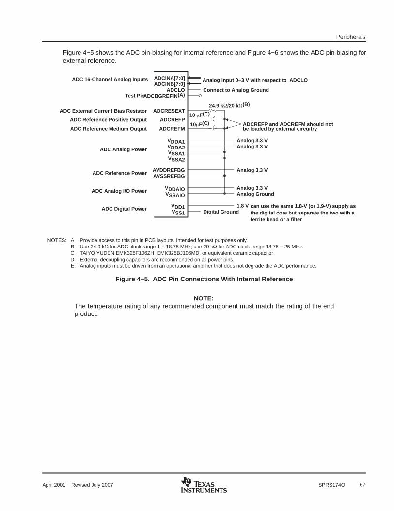
Peripherals
67April 2001 − Revised July 2007 SPRS174O
Figure 4−5 shows the ADC pin-biasing for internal reference and Figure 4−6 shows the ADC pin-biasing forexternal reference.
ADCINA[7:0]ADCINB[7:0]
ADCLOADCBGREFIN(A)
ADC External Current Bias Resistor ADCRESEXT
ADCREFP
VDDA1VDDA2VSSA1VSSA2
AVDDREFBGAVSSREFBG
VDDAIOVSSAIO
VDD1VSS1
Test Pin
ADC Reference Positive Output
ADCREFMADC Reference Medium Output
ADC Analog Power
ADC Reference Power
ADC Analog I/O Power
ADC Digital Power
Analog input 0−3 V with respect to ADCLO
Connect to Analog Ground
24.9 k/20 k(B)
10 F(C)
10 F(C)
Analog 3.3 VAnalog 3.3 V
Analog 3.3 V
Analog 3.3 VAnalog Ground
1.8 V
ADCREFP and ADCREFM should notbe loaded by external circuitry
can use the same 1.8-V (or 1.9-V) supply asthe digital core but separate the two with aferrite bead or a filter
Digital Ground
ADC 16-Channel Analog Inputs
NOTES: A. Provide access to this pin in PCB layouts. Intended for test purposes only.B. Use 24.9 kΩ for ADC clock range 1 − 18.75 MHz; use 20 kΩ for ADC clock range 18.75 − 25 MHz.C. TAIYO YUDEN EMK325F106ZH, EMK325BJ106MD, or equivalent ceramic capacitorD. External decoupling capacitors are recommended on all power pins.E. Analog inputs must be driven from an operational amplifier that does not degrade the ADC performance.
Figure 4−5. ADC Pin Connections With Internal Reference
NOTE:The temperature rating of any recommended component must match the rating of the endproduct.

Peripherals
68 April 2001 − Revised July 2007SPRS174O
ADCINA[7:0]ADCINB[7:0]
ADCLOADCBGREFIN
ADC External Current Bias Resistor ADCRESEXT
ADCREFP
VDDA1VDDA2VSSA1VSSA2
AVDDREFBGAVSSREFBG
VDDAIOVSSAIO
VDD1VSS1
Test Pin
ADC Reference Positive Input
ADCREFMADC Reference Medium Input
ADC Analog Power
ADC Reference Power
ADC Analog I/O Power
ADC Digital Power
Analog Input 0−3 V With Respect to ADCLO
Connect to Analog Ground
24.9 k20 k (C)
Analog 3.3 VAnalog 3.3 V
Analog 3.3 V
Analog 3.3 VAnalog Ground
1.8 V Can use the same 1.8-V (or 1.9-V) supply as the digital core but separate thetwo with a ferrite bead or a filter
Digital Ground
ADC 16-Channel Analog Inputs
1 F −10 F
2 V
1 V
1 F − 10 F
NOTES: A. External decoupling capacitors are recommended on all power pins.B. Analog inputs must be driven from an operational amplifier that does not degrade the ADC performance.C. Use 24.9 kΩ for ADC clock range 1 − 18.75 MHz; use 20 kΩ for ADC clock range 18.75 − 25 MHz.D. It is recommended that buffered external references be provided with a voltage difference of (ADCREFP-ADCREFM)
= 1 V 0.1% or better.
External reference is enabled using bit 8 in the ADCTRL3 Register at ADC power up. In this mode, the accuracy ofexternal reference is critical for overall gain. The voltage ADCREFP−ADCREFM will determine the overall accuracy.Do not enable internal references when external references are connected to ADCREFP and ADCREFM. See theTMS320x281x DSP Analog-to-Digital Converter (ADC) Reference Guide (literature number SPRU060) for moreinformation.
(D)
Figure 4−6. ADC Pin Connections With External Reference

Peripherals
69April 2001 − Revised July 2007 SPRS174O
The ADC operation is configured, controlled, and monitored by the registers listed in Table 4−4.
Table 4−4. ADC Registers †
NAME ADDRESSSIZE(x16) DESCRIPTION
ADCTRL1 0x00 7100 1 ADC Control Register 1
ADCTRL2 0x00 7101 1 ADC Control Register 2
ADCMAXCONV 0x00 7102 1 ADC Maximum Conversion Channels Register
ADCCHSELSEQ1 0x00 7103 1 ADC Channel Select Sequencing Control Register 1
ADCCHSELSEQ2 0x00 7104 1 ADC Channel Select Sequencing Control Register 2
ADCCHSELSEQ3 0x00 7105 1 ADC Channel Select Sequencing Control Register 3
ADCCHSELSEQ4 0x00 7106 1 ADC Channel Select Sequencing Control Register 4
ADCASEQSR 0x00 7107 1 ADC Auto-Sequence Status Register
ADCRESULT0 0x00 7108 1 ADC Conversion Result Buffer Register 0
ADCRESULT1 0x00 7109 1 ADC Conversion Result Buffer Register 1
ADCRESULT2 0x00 710A 1 ADC Conversion Result Buffer Register 2
ADCRESULT3 0x00 710B 1 ADC Conversion Result Buffer Register 3
ADCRESULT4 0x00 710C 1 ADC Conversion Result Buffer Register 4
ADCRESULT5 0x00 710D 1 ADC Conversion Result Buffer Register 5
ADCRESULT6 0x00 710E 1 ADC Conversion Result Buffer Register 6
ADCRESULT7 0x00 710F 1 ADC Conversion Result Buffer Register 7
ADCRESULT8 0x00 7110 1 ADC Conversion Result Buffer Register 8
ADCRESULT9 0x00 7111 1 ADC Conversion Result Buffer Register 9
ADCRESULT10 0x00 7112 1 ADC Conversion Result Buffer Register 10
ADCRESULT11 0x00 7113 1 ADC Conversion Result Buffer Register 11
ADCRESULT12 0x00 7114 1 ADC Conversion Result Buffer Register 12
ADCRESULT13 0x00 7115 1 ADC Conversion Result Buffer Register 13
ADCRESULT14 0x00 7116 1 ADC Conversion Result Buffer Register 14
ADCRESULT15 0x00 7117 1 ADC Conversion Result Buffer Register 15
ADCTRL3 0x00 7118 1 ADC Control Register 3
ADCST 0x00 7119 1 ADC Status Register
Reserved0x00 711C0x00 711F
4
† The above registers are Peripheral Frame 2 Registers.

Peripherals
70 April 2001 − Revised July 2007SPRS174O
4.4 Enhanced Controller Area Network (eCAN) Module
The CAN module has the following features:
• Fully compliant with CAN protocol, version 2.0B
• Supports data rates up to 1 Mbps
• Thirty-two mailboxes, each with the following properties:
− Configurable as receive or transmit− Configurable with standard or extended identifier− Has a programmable receive mask− Supports data and remote frame− Composed of 0 to 8 bytes of data− Uses a 32-bit time stamp on receive and transmit message− Protects against reception of new message− Holds the dynamically programmable priority of transmit message− Employs a programmable interrupt scheme with two interrupt levels− Employs a programmable alarm on transmission or reception time-out
• Low-power mode
• Programmable wake-up on bus activity
• Automatic reply to a remote request message
• Automatic retransmission of a frame in case of loss of arbitration or error
• 32-bit local network time counter synchronized by a specific message (communication in conjunction withmailbox 16)
• Self-test mode
− Operates in a loopback mode receiving its own message. A “dummy” acknowledge is provided,thereby eliminating the need for another node to provide the acknowledge bit.
NOTE: For a SYSCLKOUT of 150 MHz, the smallest bit rate possible is 23.4 kbps.
The 28x CAN has passed the conformance test per ISO/DIS 16845. Contact TI for details.
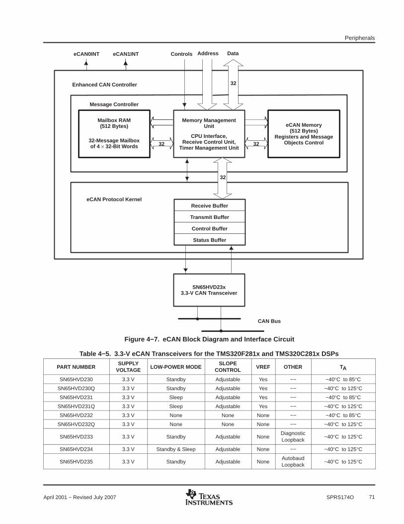
Peripherals
71April 2001 − Revised July 2007 SPRS174O
Mailbox RAM(512 Bytes)
32-Message Mailboxof 4 × 32-Bit Words
Memory ManagementUnit
CPU Interface,Receive Control Unit,
Timer Management Unit
eCAN Memory(512 Bytes)
Registers and MessageObjects Control32 32
Message Controller
32 3232 3232 32
eCAN Protocol KernelReceive Buffer
Transmit Buffer
Control Buffer
Status Buffer
Enhanced CAN Controller 32
Controls Address DataeCAN1INTeCAN0INT
32
SN65HVD23x3.3-V CAN Transceiver
CAN Bus
Figure 4−7. eCAN Block Diagram and Interface Circuit
Table 4−5. 3.3-V eCAN Transceivers for the TMS320F281x and TMS320C281x DSPs
PART NUMBERSUPPLY
VOLTAGE LOW-POWER MODESLOPE
CONTROL VREF OTHER TA
SN65HVD230 3.3 V Standby Adjustable Yes −− −40°C to 85°C
SN65HVD230Q 3.3 V Standby Adjustable Yes −− −40°C to 125°C
SN65HVD231 3.3 V Sleep Adjustable Yes −− −40°C to 85°C
SN65HVD231Q 3.3 V Sleep Adjustable Yes −− −40°C to 125°C
SN65HVD232 3.3 V None None None −− −40°C to 85°C
SN65HVD232Q 3.3 V None None None −− −40°C to 125°C
SN65HVD233 3.3 V Standby Adjustable NoneDiagnosticLoopback
−40°C to 125°C
SN65HVD234 3.3 V Standby & Sleep Adjustable None −− −40°C to 125°C
SN65HVD235 3.3 V Standby Adjustable NoneAutobaudLoopback
−40°C to 125°C

Peripherals
72 April 2001 − Revised July 2007SPRS174O
Mailbox Enable − CANME
Mailbox Direction − CANMD
Transmission Request Set − CANTRS
Transmission Request Reset − CANTRR
Transmission Acknowledge − CANTA
Abort Acknowledge − CANAA
Received Message Pending − CANRMP
Received Message Lost − CANRML
Remote Frame Pending − CANRFP
Global Acceptance Mask − CANGAM
Master Control − CANMC
Bit-Timing Configuration − CANBTC
Error and Status − CANES
Transmit Error Counter − CANTEC
Receive Error Counter − CANREC
Global Interrupt Flag 0 − CANGIF0
Global Interrupt Mask − CANGIM
Mailbox Interrupt Mask − CANMIM
Mailbox Interrupt Level − CANMIL
Overwrite Protection Control − CANOPC
TX I/O Control − CANTIOC
RX I/O Control − CANRIOC
Time Stamp Counter − CANTSC
Global Interrupt Flag 1 − CANGIF1
Time-Out Control − CANTOC
Time-Out Status − CANTOS
Reserved
eCAN Control and Status Registers
Message Identifier − MSGID61E8h−61E9h
Message Control − MSGCTRL
Message Data Low − MDL
Message Data High − MDH
Message Mailbox (16 Bytes)
Control and Status Registers6000h
603Fh
Local Acceptance Masks (LAM)(32 × 32-Bit RAM)
6040h
607Fh
6080h
60BFh
60C0h
60FFh
eCAN Memory (512 Bytes)
Message Object Time Stamps (MOTS)(32 × 32-Bit RAM)
Message Object Time-Out (MOTO)(32 × 32-Bit RAM)
Mailbox 06100h−6107h
Mailbox 16108h−610Fh
Mailbox 26110h−6117h
Mailbox 36118h−611Fh
eCAN Memory RAM (512 Bytes)
Mailbox 46120h−6127h
Mailbox 2861E0h−61E7h
Mailbox 2961E8h−61EFh
Mailbox 3061F0h−61F7h
Mailbox 3161F8h−61FFh
61EAh−61EBh
61ECh−61EDh
61EEh−61EFh
Figure 4−8. eCAN Memory Map
NOTE:If the eCAN module is not used in an application, the RAM available (LAM, MOTS, MOTO, andmailbox RAM) can be used as general-purpose RAM. The CAN module clock should beenabled for this.

Peripherals
73April 2001 − Revised July 2007 SPRS174O
The CAN registers listed in Table 4−6 are used by the CPU to configure and control the CAN controller andthe message objects. eCAN control registers only support 32-bit read/write operations. Mailbox RAM can beaccessed as 16 bits or 32 bits. 32-bit accesses are aligned to an even boundary.
Table 4−6. CAN Registers Map †
REGISTER NAME ADDRESSSIZE(x32) DESCRIPTION
CANME 0x00 6000 1 Mailbox enable
CANMD 0x00 6002 1 Mailbox direction
CANTRS 0x00 6004 1 Transmit request set
CANTRR 0x00 6006 1 Transmit request reset
CANTA 0x00 6008 1 Transmission acknowledge
CANAA 0x00 600A 1 Abort acknowledge
CANRMP 0x00 600C 1 Receive message pending
CANRML 0x00 600E 1 Receive message lost
CANRFP 0x00 6010 1 Remote frame pending
CANGAM 0x00 6012 1 Global acceptance mask
CANMC 0x00 6014 1 Master control
CANBTC 0x00 6016 1 Bit-timing configuration
CANES 0x00 6018 1 Error and status
CANTEC 0x00 601A 1 Transmit error counter
CANREC 0x00 601C 1 Receive error counter
CANGIF0 0x00 601E 1 Global interrupt flag 0
CANGIM 0x00 6020 1 Global interrupt mask
CANGIF1 0x00 6022 1 Global interrupt flag 1
CANMIM 0x00 6024 1 Mailbox interrupt mask
CANMIL 0x00 6026 1 Mailbox interrupt level
CANOPC 0x00 6028 1 Overwrite protection control
CANTIOC 0x00 602A 1 TX I/O control
CANRIOC 0x00 602C 1 RX I/O control
CANTSC 0x00 602E 1 Time stamp counter (Reserved in SCC mode)
CANTOC 0x00 6030 1 Time-out control (Reserved in SCC mode)
CANTOS 0x00 6032 1 Time-out status (Reserved in SCC mode)† These registers are mapped to Peripheral Frame 1.
Peripherals
74 April 2001 − Revised July 2007SPRS174O
4.5 Multichannel Buffered Serial Port (McBSP) Module
The McBSP module has the following features:
• Compatible to McBSP in TMS320C54x /TMS320C55x DSP devices, except the DMA features
• Full-duplex communication
• Double-buffered data registers which allow a continuous data stream
• Independent framing and clocking for receive and transmit
• External shift clock generation or an internal programmable frequency shift clock
• A wide selection of data sizes including 8-, 12-, 16-, 20-, 24-, or 32-bits
• 8-bit data transfers with LSB or MSB first
• Programmable polarity for both frame synchronization and data clocks
• HIghly programmable internal clock and frame generation
• Support A-bis mode
• Direct interface to industry-standard CODECs, Analog Interface Chips (AICs), and other seriallyconnected A/D and D/A devices
• Works with SPI-compatible devices
• Two 16 x 16-level FIFO for Transmit channel
• Two 16 x 16-level FIFO for Receive channel
The following application interfaces can be supported on the McBSP:
• T1/E1 framers
• MVIP switching-compatible and ST-BUS-compliant devices including:
− MVIP framers
− H.100 framers
− SCSA framers
− IOM-2 compliant devices
− AC97-compliant devices (the necessary multiphase frame synchronization capability is provided.)
− IIS-compliant devices
• McBSP clock rate = CLKG = CLKSRG(1 CLKGDIV)
, where CLKSRG source could be LSPCLK, CLKX, or
CLKR.†
TMS320C54x and TMS320C55x are trademarks of Texas Instruments.† Serial port performance is limited by I/O buffer switching speed. Internal prescalers must be adjusted such that the peripheral speed is less
than the I/O buffer speed limit—20-MHz maximum.
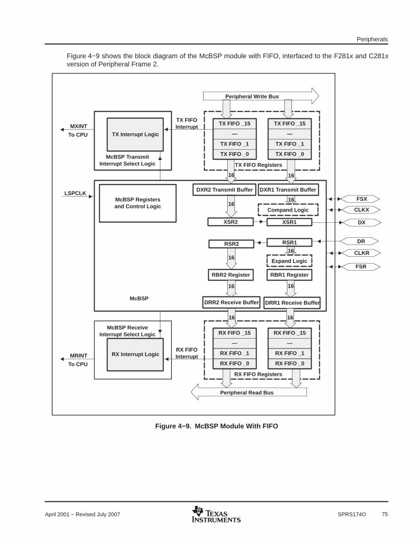
Peripherals
75April 2001 − Revised July 2007 SPRS174O
Figure 4−9 shows the block diagram of the McBSP module with FIFO, interfaced to the F281x and C281xversion of Peripheral Frame 2.
McBSP ReceiveInterrupt Select Logic
DX
DR
Expand Logic
DRR1 Receive Buffer
RX FIFOInterrupt
DRR2 Receive Buffer
RX FIFO Registers
RBR1 RegisterRBR2 Register
McBSP Registersand Control Logic
CLKX
FSX
CLKR
FSR
16
Compand Logic
DXR2 Transmit Buffer
RSR1
XSR2 XSR1
Peripheral Read Bus
16
1616
1616
RSR2
DXR1 Transmit Buffer
16
LSPCLK
MRINT
To CPU
McBSP
RX Interrupt Logic
RX FIFO _15
—
RX FIFO _1
RX FIFO _0
RX FIFO _15
—
RX FIFO _1
RX FIFO _0
McBSP TransmitInterrupt Select Logic
TX FIFOInterrupt
TX FIFO Registers
MXINT
To CPU TX Interrupt Logic
16 16
16
TX FIFO _15
—
TX FIFO _1
TX FIFO _0
TX FIFO _15
—
TX FIFO _1
TX FIFO _0
Peripheral Write Bus
Figure 4−9. McBSP Module With FIFO
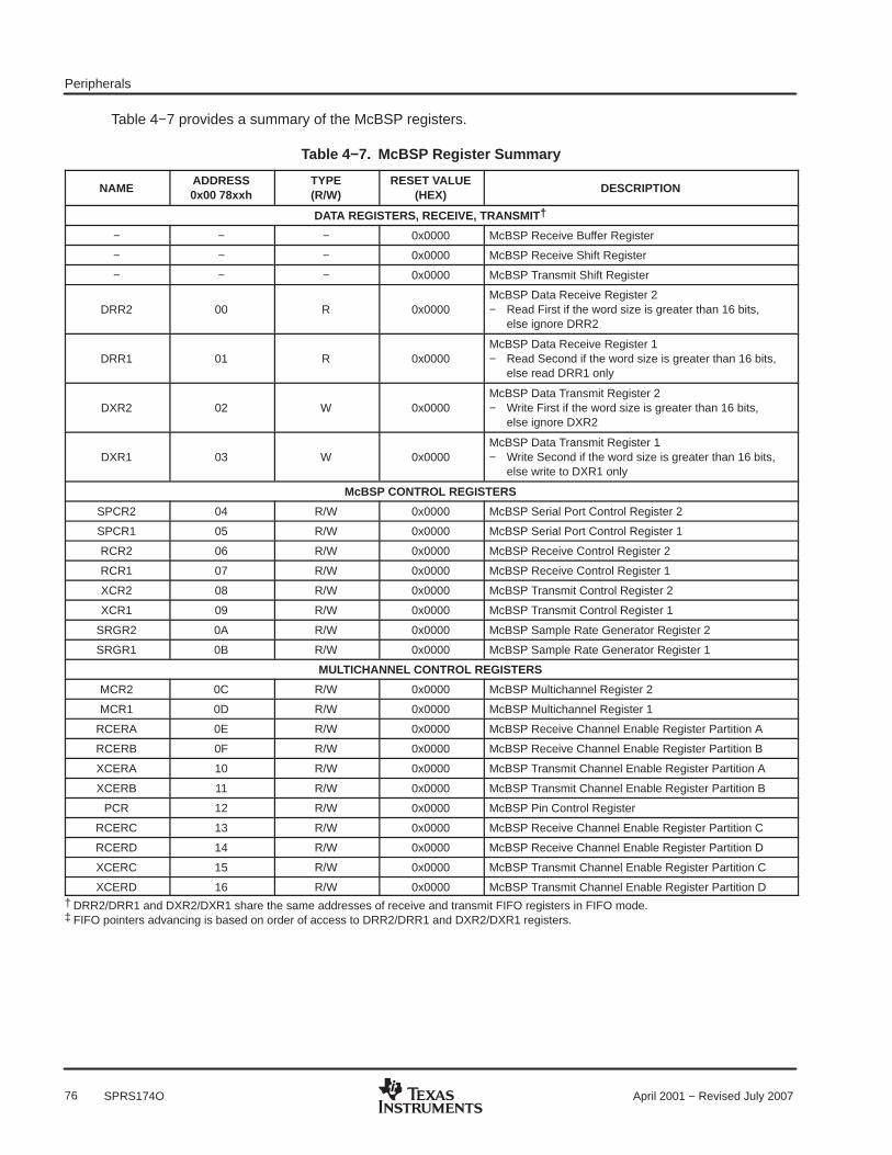
Peripherals
76 April 2001 − Revised July 2007SPRS174O
Table 4−7 provides a summary of the McBSP registers.
Table 4−7. McBSP Register Summary
NAMEADDRESS0x00 78xxh
TYPE(R/W)
RESET VALUE(HEX) DESCRIPTION
DATA REGISTERS, RECEIVE, TRANSMIT †
− − − 0x0000 McBSP Receive Buffer Register
− − − 0x0000 McBSP Receive Shift Register
− − − 0x0000 McBSP Transmit Shift Register
DRR2 00 R 0x0000McBSP Data Receive Register 2− Read First if the word size is greater than 16 bits,
else ignore DRR2
DRR1 01 R 0x0000McBSP Data Receive Register 1− Read Second if the word size is greater than 16 bits,
else read DRR1 only
DXR2 02 W 0x0000McBSP Data Transmit Register 2− Write First if the word size is greater than 16 bits,
else ignore DXR2
DXR1 03 W 0x0000McBSP Data Transmit Register 1− Write Second if the word size is greater than 16 bits,
else write to DXR1 only
McBSP CONTROL REGISTERS
SPCR2 04 R/W 0x0000 McBSP Serial Port Control Register 2
SPCR1 05 R/W 0x0000 McBSP Serial Port Control Register 1
RCR2 06 R/W 0x0000 McBSP Receive Control Register 2
RCR1 07 R/W 0x0000 McBSP Receive Control Register 1
XCR2 08 R/W 0x0000 McBSP Transmit Control Register 2
XCR1 09 R/W 0x0000 McBSP Transmit Control Register 1
SRGR2 0A R/W 0x0000 McBSP Sample Rate Generator Register 2
SRGR1 0B R/W 0x0000 McBSP Sample Rate Generator Register 1
MULTICHANNEL CONTROL REGISTERS
MCR2 0C R/W 0x0000 McBSP Multichannel Register 2
MCR1 0D R/W 0x0000 McBSP Multichannel Register 1
RCERA 0E R/W 0x0000 McBSP Receive Channel Enable Register Partition A
RCERB 0F R/W 0x0000 McBSP Receive Channel Enable Register Partition B
XCERA 10 R/W 0x0000 McBSP Transmit Channel Enable Register Partition A
XCERB 11 R/W 0x0000 McBSP Transmit Channel Enable Register Partition B
PCR 12 R/W 0x0000 McBSP Pin Control Register
RCERC 13 R/W 0x0000 McBSP Receive Channel Enable Register Partition C
RCERD 14 R/W 0x0000 McBSP Receive Channel Enable Register Partition D
XCERC 15 R/W 0x0000 McBSP Transmit Channel Enable Register Partition C
XCERD 16 R/W 0x0000 McBSP Transmit Channel Enable Register Partition D† DRR2/DRR1 and DXR2/DXR1 share the same addresses of receive and transmit FIFO registers in FIFO mode.‡ FIFO pointers advancing is based on order of access to DRR2/DRR1 and DXR2/DXR1 registers.
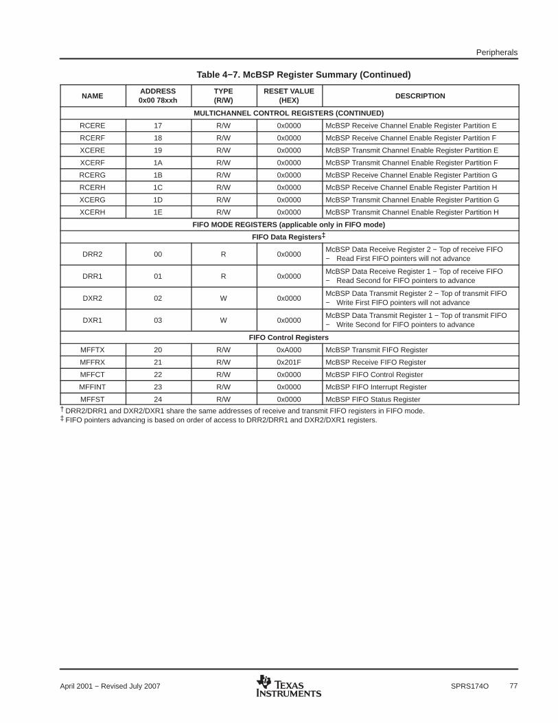
Peripherals
77April 2001 − Revised July 2007 SPRS174O
Table 4−7. McBSP Register Summary (Continued)
NAMEADDRESS0x00 78xxh
TYPE(R/W)
RESET VALUE(HEX) DESCRIPTION
MULTICHANNEL CONTROL REGISTERS (CONTINUED)
RCERE 17 R/W 0x0000 McBSP Receive Channel Enable Register Partition E
RCERF 18 R/W 0x0000 McBSP Receive Channel Enable Register Partition F
XCERE 19 R/W 0x0000 McBSP Transmit Channel Enable Register Partition E
XCERF 1A R/W 0x0000 McBSP Transmit Channel Enable Register Partition F
RCERG 1B R/W 0x0000 McBSP Receive Channel Enable Register Partition G
RCERH 1C R/W 0x0000 McBSP Receive Channel Enable Register Partition H
XCERG 1D R/W 0x0000 McBSP Transmit Channel Enable Register Partition G
XCERH 1E R/W 0x0000 McBSP Transmit Channel Enable Register Partition H
FIFO MODE REGISTERS (applicable only in FIFO mode)
FIFO Data Registers ‡
DRR2 00 R 0x0000McBSP Data Receive Register 2 − Top of receive FIFO− Read First FIFO pointers will not advance
DRR1 01 R 0x0000McBSP Data Receive Register 1 − Top of receive FIFO− Read Second for FIFO pointers to advance
DXR2 02 W 0x0000McBSP Data Transmit Register 2 − Top of transmit FIFO− Write First FIFO pointers will not advance
DXR1 03 W 0x0000McBSP Data Transmit Register 1 − Top of transmit FIFO− Write Second for FIFO pointers to advance
FIFO Control Registers
MFFTX 20 R/W 0xA000 McBSP Transmit FIFO Register
MFFRX 21 R/W 0x201F McBSP Receive FIFO Register
MFFCT 22 R/W 0x0000 McBSP FIFO Control Register
MFFINT 23 R/W 0x0000 McBSP FIFO Interrupt Register
MFFST 24 R/W 0x0000 McBSP FIFO Status Register† DRR2/DRR1 and DXR2/DXR1 share the same addresses of receive and transmit FIFO registers in FIFO mode.‡ FIFO pointers advancing is based on order of access to DRR2/DRR1 and DXR2/DXR1 registers.
Peripherals
78 April 2001 − Revised July 2007SPRS174O
4.6 Serial Communications Interface (SCI) Module
The F281x and C281x devices include two serial communications interface (SCI) modules. The SCI modulessupport digital communications between the CPU and other asynchronous peripherals that use the standardnon-return-to-zero (NRZ) format. The SCI receiver and transmitter are double-buffered, and each has its ownseparate enable and interrupt bits. Both can be operated independently or simultaneously in the full-duplexmode. To ensure data integrity, the SCI checks received data for break detection, parity, overrun, and framingerrors. The bit rate is programmable to over 65000 different speeds through a 16-bit baud-select register.
Features of each SCI module include:
• Two external pins:
− SCITXD: SCI transmit-output pin
− SCIRXD: SCI receive-input pin
NOTE: Both pins can be used as GPIO if not used for SCI.
• Baud rate programmable to 64K different rates†
− Baud rate = LSPCLK(BRR 1) * 8
, when BRR ≠ 0
= LSPCLK16
, when BRR = 0
• Data-word format
− One start bit
− Data-word length programmable from one to eight bits
− Optional even/odd/no parity bit
− One or two stop bits
• Four error-detection flags: parity, overrun, framing, and break detection
• Two wake-up multiprocessor modes: idle-line and address bit
• Half- or full-duplex operation
• Double-buffered receive and transmit functions
• Transmitter and receiver operations can be accomplished through interrupt-driven or polled algorithmswith status flags.
− Transmitter: TXRDY flag (transmitter-buffer register is ready to receive another character) andTX EMPTY flag (transmitter-shift register is empty)
− Receiver: RXRDY flag (receiver-buffer register is ready to receive another character), BRKDT flag(break condition occurred), and RX ERROR flag (monitoring four interrupt conditions)
• Separate enable bits for transmitter and receiver interrupts (except BRKDT)
• Max bit rate 75 MHz
16 4.688 106 bs
† Serial port performance is limited by I/O buffer switching speed. Internal prescalers must be adjusted such that the peripheral speed is lessthan the I/O buffer speed limit—20 MHz maximum.

Peripherals
79April 2001 − Revised July 2007 SPRS174O
• NRZ (non-return-to-zero) format
• Ten SCI module control registers located in the control register frame beginning at address 7050h
NOTE: All registers in this module are 8-bit registers that are connected to Peripheral Frame 2. When aregister is accessed, the register data is in the lower byte (7−0), and the upper byte (15−8) is read aszeros. Writing to the upper byte has no effect.
Enhanced features:
• Auto baud-detect hardware logic
• 16-level transmit/receive FIFO
The SCI port operation is configured and controlled by the registers listed in Table 4−8 and Table 4−9.
Table 4−8. SCI-A Registers †
NAME ADDRESS SIZE (x16) DESCRIPTION
SCICCRA 0x00 7050 1 SCI-A Communications Control Register
SCICTL1A 0x00 7051 1 SCI-A Control Register 1
SCIHBAUDA 0x00 7052 1 SCI-A Baud Register, High Bits
SCILBAUDA 0x00 7053 1 SCI-A Baud Register, Low Bits
SCICTL2A 0x00 7054 1 SCI-A Control Register 2
SCIRXSTA 0x00 7055 1 SCI-A Receive Status Register
SCIRXEMUA 0x00 7056 1 SCI-A Receive Emulation Data Buffer Register
SCIRXBUFA 0x00 7057 1 SCI-A Receive Data Buffer Register
SCITXBUFA 0x00 7059 1 SCI-A Transmit Data Buffer Register
SCIFFTXA 0x00 705A 1 SCI-A FIFO Transmit Register
SCIFFRXA 0x00 705B 1 SCI-A FIFO Receive Register
SCIFFCTA 0x00 705C 1 SCI-A FIFO Control Register
SCIPRIA 0x00 705F 1 SCI-A Priority Control Register
† Shaded registers are new registers for the FIFO mode.
Table 4−9. SCI-B Registers †‡
NAME ADDRESS SIZE (x16) DESCRIPTION
SCICCRB 0x00 7750 1 SCI-B Communications Control Register
SCICTL1B 0x00 7751 1 SCI-B Control Register 1
SCIHBAUDB 0x00 7752 1 SCI-B Baud Register, High Bits
SCILBAUDB 0x00 7753 1 SCI-B Baud Register, Low Bits
SCICTL2B 0x00 7754 1 SCI-B Control Register 2
SCIRXSTB 0x00 7755 1 SCI-B Receive Status Register
SCIRXEMUB 0x00 7756 1 SCI-B Receive Emulation Data Buffer Register
SCIRXBUFB 0x00 7757 1 SCI-B Receive Data Buffer Register
SCITXBUFB 0x00 7759 1 SCI-B Transmit Data Buffer Register
SCIFFTXB 0x00 775A 1 SCI-B FIFO Transmit Register
SCIFFRXB 0x00 775B 1 SCI-B FIFO Receive Register
SCIFFCTB 0x00 775C 1 SCI-B FIFO Control Register
SCIPRIB 0x00 775F 1 SCI-B Priority Control Register
† Shaded registers are new registers for the FIFO mode.‡ Registers in this table are mapped to peripheral bus 16 space. This space only allows 16-bit accesses. 32-bit accesses produce undefined results.

Peripherals
80 April 2001 − Revised July 2007SPRS174O
Figure 4−10 shows the SCI module block diagram.
TX FIFO _0
LSPCLK
WUT
Frame Format and Mode
Even/Odd EnableParity
SCI RX Interrupt select logic
BRKDT
RXRDY
SCIRXST.6
SCICTL1.3
8SCICTL2.1
RX/BK INT ENA
SCIRXD
SCIRXST.1
TXENA
SCI TX Interrupt select logic
TX EMPTY
TXRDY
SCICTL2.0
TX INT ENA
SCITXD
RXENA
SCIRXD
RXWAKE
SCICTL1.6
RX ERR INT ENA
TXWAKE
SCITXD
SCICCR.6 SCICCR.5
SCITXBUF.7−0
SCIHBAUD. 15 − 8
Baud RateMSbyteRegister
SCILBAUD. 7 − 0
Transmitter−DataBuffer Register
8 SCICTL2.6
SCICTL2.7
Baud RateLSbyte
Register
RXSHFRegister
TXSHFRegister
SCIRXST.5
1 TX FIFO _1
−−−−−TX FIFO _15
8
TX FIFO registers
TX FIFO
TX InterruptLogic
TXINT
SCIFFTX.14
RX FIFO _15
SCIRXBUF.7−0
Receive DataBuffer registerSCIRXBUF.7−0
−−−−−RX FIFO_1
RX FIFO _0
8
RX FIFO registers
SCICTL1.0
RX InterruptLogic
RXINT
RX FIFO
SCIFFRX.15
RXFFOVF
RX Error
SCIRXST.7
PEFE OERX Error
SCIRXST.4 − 2
To CPU
To CPU
AutoBaud Detect logic
SCICTL1.1
SCIFFENA
Interrupts
Interrupts
Figure 4−10. Serial Communications Interface (SCI) Module Block Diagram
Peripherals
81April 2001 − Revised July 2007 SPRS174O
4.7 Serial Peripheral Interface (SPI) Module
The F281x and C281x devices include the four-pin serial peripheral interface (SPI) module. The SPI is ahigh-speed, synchronous serial I/O port that allows a serial bit stream of programmed length (one to sixteenbits) to be shifted into and out of the device at a programmable bit-transfer rate. Normally, the SPI is used forcommunications between the DSP controller and external peripherals or another processor. Typicalapplications include external I/O or peripheral expansion through devices such as shift registers, displaydrivers, and ADCs. Multidevice communications are supported by the master/slave operation of the SPI.
The SPI module features include:
• Four external pins:
− SPISOMI: SPI slave-output/master-input pin
− SPISIMO: SPI slave-input/master-output pin
− SPISTE: SPI slave transmit-enable pin
− SPICLK: SPI serial-clock pin
NOTE: All four pins can be used as GPIO, if the SPI module is not used.
• Two operational modes: master and slave
• Baud rate: 125 different programmable rates
− Baud rate = LSPCLK(SPIBRR 1)
, when SPIBRR ≠ 0
= LSPCLK4
, when SPIBRR = 0, 1, 2, 3
Serial port performance is limited by I/O buffer switching speed. Internal prescalers must be adjustedsuch that the peripheral speed is less than the I/O buffer speed limit—20 MHz maximum.
• Data word length: one to sixteen data bits
• Four clocking schemes (controlled by clock polarity and clock phase bits) include:
− Falling edge without phase delay: SPICLK active-high. SPI transmits data on the falling edge of theSPICLK signal and receives data on the rising edge of the SPICLK signal.
− Falling edge with phase delay: SPICLK active-high. SPI transmits data one half-cycle ahead of thefalling edge of the SPICLK signal and receives data on the falling edge of the SPICLK signal.
− Rising edge without phase delay: SPICLK inactive-low. SPI transmits data on the rising edge of theSPICLK signal and receives data on the falling edge of the SPICLK signal.
− Rising edge with phase delay: SPICLK inactive-low. SPI transmits data one half-cycle ahead of thefalling edge of the SPICLK signal and receives data on the rising edge of the SPICLK signal.
• Simultaneous receive and transmit operation (transmit function can be disabled in software)
• Transmitter and receiver operations are accomplished through either interrupt-driven or polledalgorithms.
• Nine SPI module control registers: Located in control register frame beginning at address 7040h.
NOTE: All registers in this module are 16-bit registers that are connected to Peripheral Frame 2. When aregister is accessed, the register data is in the lower byte (7−0), and the upper byte (15−8) is read aszeros. Writing to the upper byte has no effect.
Enhanced feature:
• 16-level transmit/receive FIFO
• Delayed transmit control
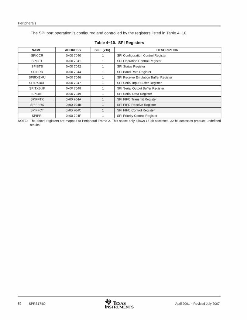
Peripherals
82 April 2001 − Revised July 2007SPRS174O
The SPI port operation is configured and controlled by the registers listed in Table 4−10.
Table 4−10. SPI Registers
NAME ADDRESS SIZE (x16) DESCRIPTION
SPICCR 0x00 7040 1 SPI Configuration Control Register
SPICTL 0x00 7041 1 SPI Operation Control Register
SPISTS 0x00 7042 1 SPI Status Register
SPIBRR 0x00 7044 1 SPI Baud Rate Register
SPIRXEMU 0x00 7046 1 SPI Receive Emulation Buffer Register
SPIRXBUF 0x00 7047 1 SPI Serial Input Buffer Register
SPITXBUF 0x00 7048 1 SPI Serial Output Buffer Register
SPIDAT 0x00 7049 1 SPI Serial Data Register
SPIFFTX 0x00 704A 1 SPI FIFO Transmit Register
SPIFFRX 0x00 704B 1 SPI FIFO Receive Register
SPIFFCT 0x00 704C 1 SPI FIFO Control Register
SPIPRI 0x00 704F 1 SPI Priority Control Register
NOTE: The above registers are mapped to Peripheral Frame 2. This space only allows 16-bit accesses. 32-bit accesses produce undefinedresults.

Peripherals
83April 2001 − Revised July 2007 SPRS174O
Figure 4−11 is a block diagram of the SPI in slave mode.
S
SPICTL.0
SPI INT FLAGSPI INT
ENA
SPISTS.6
S
ClockPolarity
Talk
LSPCLK
456 123 0
0123
SPI Bit Rate
State Control
SPIRXBUFBuffer Register
ClockPhase
ReceiverOverrun Flag
SPICTL.4
OverrunINT ENA
SPICCR.3 − 0
SPIBRR.6 − 0 SPICCR.6 SPICTL.3
SPIDAT.15 − 0
SPICTL.1
M
S
M
Master/Slave
SPISTS.7
SPIDATData Register
M
S
SPICTL.2SPI Char
SPISIMO
SPISOMI
SPICLK
SW2
S
M
M
S
SW3
To CPU
M
SW1
SPITXBUFBuffer Register
RX FIFO _0RX FIFO _1
−−−−−RX FIFO _15
TX FIFO registers
TX FIFO _0TX FIFO _1−−−−−TX FIFO _15
RX FIFO registers
16
16
16
TX InterruptLogic
RX InterruptLogic
SPIINT/SPIRXINT
SPITXINT
SPIFFOVF FLAG
SPIFFRX.15
16
TX FIFO Interrupt
RX FIFO Interrupt
SPIRXBUF
SPITXBUF
SPIFFTX.14
SPIFFENA
SPISTE†
† SPISTE is driven low by the master for a slave device.
Figure 4−11. Serial Peripheral Interface Module Block Diagram (Slave Mode)
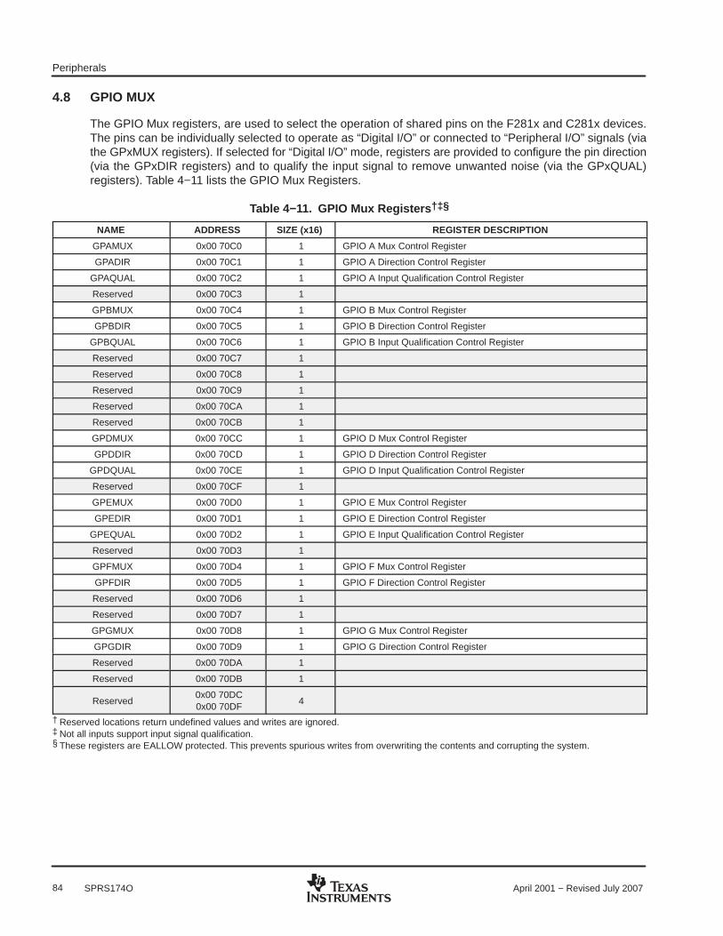
Peripherals
84 April 2001 − Revised July 2007SPRS174O
4.8 GPIO MUX
The GPIO Mux registers, are used to select the operation of shared pins on the F281x and C281x devices.The pins can be individually selected to operate as “Digital I/O” or connected to “Peripheral I/O” signals (viathe GPxMUX registers). If selected for “Digital I/O” mode, registers are provided to configure the pin direction(via the GPxDIR registers) and to qualify the input signal to remove unwanted noise (via the GPxQUAL)registers). Table 4−11 lists the GPIO Mux Registers.
Table 4−11. GPIO Mux Registers †‡§
NAME ADDRESS SIZE (x16) REGISTER DESCRIPTION
GPAMUX 0x00 70C0 1 GPIO A Mux Control Register
GPADIR 0x00 70C1 1 GPIO A Direction Control Register
GPAQUAL 0x00 70C2 1 GPIO A Input Qualification Control Register
Reserved 0x00 70C3 1
GPBMUX 0x00 70C4 1 GPIO B Mux Control Register
GPBDIR 0x00 70C5 1 GPIO B Direction Control Register
GPBQUAL 0x00 70C6 1 GPIO B Input Qualification Control Register
Reserved 0x00 70C7 1
Reserved 0x00 70C8 1
Reserved 0x00 70C9 1
Reserved 0x00 70CA 1
Reserved 0x00 70CB 1
GPDMUX 0x00 70CC 1 GPIO D Mux Control Register
GPDDIR 0x00 70CD 1 GPIO D Direction Control Register
GPDQUAL 0x00 70CE 1 GPIO D Input Qualification Control Register
Reserved 0x00 70CF 1
GPEMUX 0x00 70D0 1 GPIO E Mux Control Register
GPEDIR 0x00 70D1 1 GPIO E Direction Control Register
GPEQUAL 0x00 70D2 1 GPIO E Input Qualification Control Register
Reserved 0x00 70D3 1
GPFMUX 0x00 70D4 1 GPIO F Mux Control Register
GPFDIR 0x00 70D5 1 GPIO F Direction Control Register
Reserved 0x00 70D6 1
Reserved 0x00 70D7 1
GPGMUX 0x00 70D8 1 GPIO G Mux Control Register
GPGDIR 0x00 70D9 1 GPIO G Direction Control Register
Reserved 0x00 70DA 1
Reserved 0x00 70DB 1
Reserved0x00 70DC0x00 70DF
4
† Reserved locations return undefined values and writes are ignored.‡ Not all inputs support input signal qualification.§ These registers are EALLOW protected. This prevents spurious writes from overwriting the contents and corrupting the system.

Peripherals
85April 2001 − Revised July 2007 SPRS174O
If configured for ”Digital I/O” mode, additional registers are provided for setting individual I/O signals (via theGPxSET registers), for clearing individual I/O signals (via the GPxCLEAR registers), for toggling individual I/Osignals (via the GPxTOGGLE registers), or for reading/writing to the individual I/O signals (via the GPxDATregisters). Table 4−12 lists the GPIO Data Registers. For more information, see the TMS320x281x SystemControl and Interrupts Reference Guide (literature number SPRU078).
Table 4−12. GPIO Data Registers †‡
NAME ADDRESS SIZE (x16) REGISTER DESCRIPTION
GPADAT 0x00 70E0 1 GPIO A Data Register
GPASET 0x00 70E1 1 GPIO A Set Register
GPACLEAR 0x00 70E2 1 GPIO A Clear Register
GPATOGGLE 0x00 70E3 1 GPIO A Toggle Register
GPBDAT 0x00 70E4 1 GPIO B Data Register
GPBSET 0x00 70E5 1 GPIO B Set Register
GPBCLEAR 0x00 70E6 1 GPIO B Clear Register
GPBTOGGLE 0x00 70E7 1 GPIO B Toggle Register
Reserved 0x00 70E8 1
Reserved 0x00 70E9 1
Reserved 0x00 70EA 1
Reserved 0x00 70EB 1
GPDDAT 0x00 70EC 1 GPIO D Data Register
GPDSET 0x00 70ED 1 GPIO D Set Register
GPDCLEAR 0x00 70EE 1 GPIO D Clear Register
GPDTOGGLE 0x00 70EF 1 GPIO D Toggle Register
GPEDAT 0x00 70F0 1 GPIO E Data Register
GPESET 0x00 70F1 1 GPIO E Set Register
GPECLEAR 0x00 70F2 1 GPIO E Clear Register
GPETOGGLE 0x00 70F3 1 GPIO E Toggle Register
GPFDAT 0x00 70F4 1 GPIO F Data Register
GPFSET 0x00 70F5 1 GPIO F Set Register
GPFCLEAR 0x00 70F6 1 GPIO F Clear Register
GPFTOGGLE 0x00 70F7 1 GPIO F Toggle Register
GPGDAT 0x00 70F8 1 GPIO G Data Register
GPGSET 0x00 70F9 1 GPIO G Set Register
GPGCLEAR 0x00 70FA 1 GPIO G Clear Register
GPGTOGGLE 0x00 70FB 1 GPIO G Toggle Register
Reserved0x00 70FC0x00 70FF
4
† Reserved locations will return undefined values and writes will be ignored.‡ These registers are NOT EALLOW protected. The above registers will typically be accessed regularly by the user.

Peripherals
86 April 2001 − Revised July 2007SPRS174O
Figure 4−12 shows how the various register bits select the various modes of operation for GPIO function.
Peripheral I/O
MUX
0 1
MUX
10
PIN
Internal (Pullup or Pulldown)
Digital I/O
XRS
High-ImpedanceEnable (1)
High-Impedance
Control
GPxDIRRegister Bit
GPxMUXRegister Bit
GPxQUALRegister
GPxDAT/SET/CLEAR/TOGGLERegister Bit(s)
Input Qualification SYSCLKOUT
NOTES: A. In the GPIO mode, when the GPIO pin is configured for output operation, reading the GPxDAT data register only gives the valuewritten, not the value at the pin. In the peripheral mode, the state of the pin can be read through the GPxDAT register, provided thecorresponding direction bit is zero (input mode).
B. Some selected input signals are qualified by the SYSCLKOUT. The GPxQUAL register specifies the qualification sampling period.The sampling window is 6 samples wide and the output is only changed when all samples are the same (all 0’s or all 1’s). This featureremoves unwanted spikes from the input signal.
Figure 4−12. GPIO/Peripheral Pin Multiplexing
NOTE:The input function of the GPIO pin and the input path to the peripheral are always enabled.It is the output function of the GPIO pin that is multiplexed with the output path of the primary(peripheral) function. Since the output buffer of a pin connects back to the input buffer, anyGPIO signal present at the pin will be propagated to the peripheral module as well. Therefore,when a pin is configured for GPIO operation, the corresponding peripheral functionality (andinterrupt-generating capability) must be disabled. Otherwise, interrupts may be inadvertentlytriggered. This is especially critical when the PDPINTA and PDPINTB pins are used as GPIOpins, since a value of zero for GPDDAT.0 or GPDDAT.5 (PDPINTx) will put PWM pins in ahigh-impedance state. The CxTRIP and TxCTRIP pins will also put the corresponding PWMpins in high impedance, if they are driven low (as GPIO pins) and bit EXTCONx.0 = 1.

Development Support
87April 2001 − Revised July 2007 SPRS174O
5 Development Support
Texas Instruments (TI) offers an extensive line of development tools for the C28x generation of DSPs,including tools to evaluate the performance of the processors, generate code, develop algorithmimplementations, and fully integrate and debug software and hardware modules.
The following products support development of F281x- and C281x-based applications:
Software Development Tools
• Code Composer Studio Integrated Development Environment (IDE)
− C/C++ Compiler− Code generation tools− Assembler/Linker− Cycle Accurate Simulator
• Application algorithms
• Sample applications code
Hardware Development Tools
• 2812 eZdsp• JTAG-based emulators − SPI515, XDS510PP, XDS510PP Plus, XDS510 USB• Universal 5-V dc power supply• Documentation and cables
5.1 Device and Development Support Tool Nomenclature
To designate the stages in the product development cycle, TI assigns prefixes to the part numbers of all[TMS320] DSP devices and support tools. Each [TMS320] DSP commercial family member has one of threeprefixes: TMX, TMP, or TMS (e.g., TMS320F2812GHH). Texas Instruments recommends two of threepossible prefix designators for its support tools: TMDX and TMDS. These prefixes represent evolutionarystages of product development from engineering prototypes (TMX/TMDX) through fully qualified productiondevices/tools (TMS/TMDS).
TMX Experimental device that is not necessarily representative of the final device’s electrical specifications
TMP Final silicon die that conforms to the device’s electrical specifications but has not completed qualityand reliability verification
TMS Fully qualified production device
Support tool development evolutionary flow:
TMDX Development-support product that has not yet completed Texas Instruments internal qualificationtesting.
TMDS Fully qualified development-support product
TMX and TMP devices and TMDX development-support tools are shipped against the following disclaimer:
“Developmental product is intended for internal evaluation purposes.“
TMS devices and TMDS development-support tools have been characterized fully, and the quality andreliability of the device have been demonstrated fully. TI’s standard warranty applies.
Predictions show that prototype devices (TMX or TMP) have a greater failure rate than the standardproduction devices. Texas Instruments recommends that these devices not be used in any production systembecause their expected end-use failure rate still is undefined. Only qualified production devices are to be used.
TMS320 is a trademark of Texas Instruments.
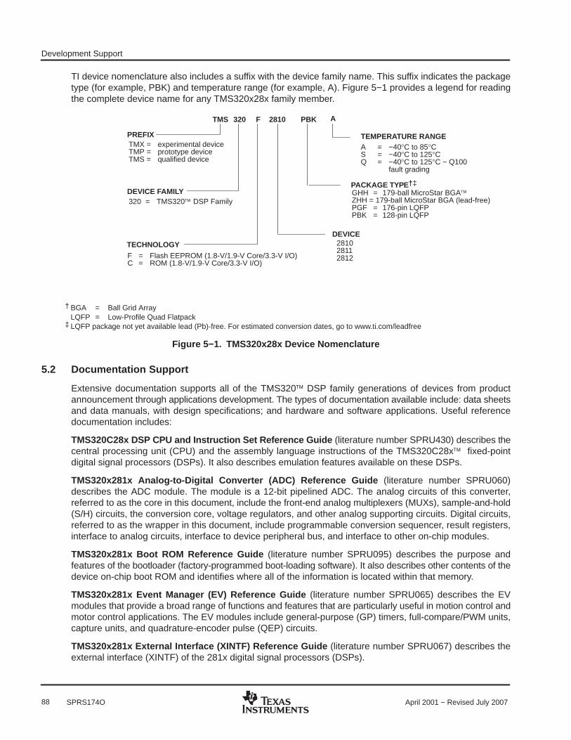
Development Support
88 April 2001 − Revised July 2007SPRS174O
TI device nomenclature also includes a suffix with the device family name. This suffix indicates the packagetype (for example, PBK) and temperature range (for example, A). Figure 5−1 provides a legend for readingthe complete device name for any TMS320x28x family member.
PREFIX
TMS 320 F 2810 PBK
TMX = experimental deviceTMP = prototype deviceTMS = qualified device
DEVICE FAMILY320 = TMS320 DSP Family
TECHNOLOGY
PACKAGE TYPE†‡GHH = 179-ball MicroStar BGAZHH = 179-ball MicroStar BGA (lead-free)PGF = 176-pin LQFPPBK = 128-pin LQFP
F = Flash EEPROM (1.8-V/1.9-V Core/3.3-V I/O)C = ROM (1.8-V/1.9-V Core/3.3-V I/O)
DEVICE281028112812
† BGA = Ball Grid ArrayLQFP = Low-Profile Quad Flatpack
‡ LQFP package not yet available lead (Pb)-free. For estimated conversion dates, go to www.ti.com/leadfree
TEMPERATURE RANGEA = −40°C to 85°CS = −40°C to 125°CQ = −40°C to 125°C − Q100
fault grading
A
Figure 5−1. TMS320x28x Device Nomenclature
5.2 Documentation Support
Extensive documentation supports all of the TMS320 DSP family generations of devices from productannouncement through applications development. The types of documentation available include: data sheetsand data manuals, with design specifications; and hardware and software applications. Useful referencedocumentation includes:
TMS320C28x DSP CPU and Instruction Set Reference Guide (literature number SPRU430) describes thecentral processing unit (CPU) and the assembly language instructions of the TMS320C28x fixed-pointdigital signal processors (DSPs). It also describes emulation features available on these DSPs.
TMS320x281x Analog-to-Digital Converter (ADC) Reference Guide (literature number SPRU060)describes the ADC module. The module is a 12-bit pipelined ADC. The analog circuits of this converter,referred to as the core in this document, include the front-end analog multiplexers (MUXs), sample-and-hold(S/H) circuits, the conversion core, voltage regulators, and other analog supporting circuits. Digital circuits,referred to as the wrapper in this document, include programmable conversion sequencer, result registers,interface to analog circuits, interface to device peripheral bus, and interface to other on-chip modules.
TMS320x281x Boot ROM Reference Guide (literature number SPRU095) describes the purpose andfeatures of the bootloader (factory-programmed boot-loading software). It also describes other contents of thedevice on-chip boot ROM and identifies where all of the information is located within that memory.
TMS320x281x Event Manager (EV) Reference Guide (literature number SPRU065) describes the EVmodules that provide a broad range of functions and features that are particularly useful in motion control andmotor control applications. The EV modules include general-purpose (GP) timers, full-compare/PWM units,capture units, and quadrature-encoder pulse (QEP) circuits.
TMS320x281x External Interface (XINTF) Reference Guide (literature number SPRU067) describes theexternal interface (XINTF) of the 281x digital signal processors (DSPs).

Development Support
89April 2001 − Revised July 2007 SPRS174O
TMS320x281x Multi-channel Buffered Serial Ports (McBSPs) Reference Guide (literature numberSPRU061) describes the McBSP) available on the 281x devices. The McBSPs allow direct interface betweena DSP and other devices in a system.
TMS320x281x System Control and Interrupts Reference Guide (literature number SPRU078) describesthe various interrupts and system control features of the 281x digital signal processors (DSPs).
TMS320x281x, 280x Enhanced Controller Area Network (eCAN) Reference Guide (literature numberSPRU074) describes the eCAN that uses established protocol to communicate serially with other controllersin electrically noisy environments. With 32 fully configurable mailboxes and time-stamping feature, the eCANmodule provides a versatile and robust serial communication interface. The eCAN module implemented inthe C28x DSP is compatible with the CAN 2.0B standard (active).
TMS320x281x, 280x Peripheral Reference Guide (literature number SPRU566) describes the peripheralreference guides of the 28x digital signal processors (DSPs).
TMS320x281x, 280x Serial Communication Interface (SCI) Reference Guide (literature numberSPRU051) describes the SCI that is a two-wire asynchronous serial port, commonly known as a UART. TheSCI modules support digital communications between the CPU and other asynchronous peripherals that usethe standard non-return-to-zero (NRZ) format.
TMS320x281x, 280x Serial Peripheral Interface (SPI) Reference Guide (literature number SPRU059)describes the SPI − a high-speed synchronous serial input/output (I/O) port that allows a serial bit stream ofprogrammed length (one to sixteen bits) to be shifted into and out of the device at a programmed bit-transferrate. The SPI is used for communications between the DSP controller and external peripherals or anothercontroller.
3.3 V DSP for Digital Motor Control Application Report (literature number SPRA550). The applicationreport first describes a scenario of a 3.3-V-only motor controller indicating that for most applications, nosignificant issue of interfacing between 3.3 V and 5 V exists. Cost-effective 3.3-V/5-V interfacing techniquesare then discussed for the situations where such interfacing is needed. On-chip 3.3-V analog-to-digitalconverter (ADC) versus 5-V ADC is also discussed. Guidelines for component layout and printed circuit board(PCB) design that can reduce system noise and EMI effects are summarized in the last section.
The TMS320C28x Instruction Set Simulator Technical Overview (literature number SPRU608) describesthe simulator, available within the Code Composer Studio for TMS320C2000 IDE, that simulates theinstruction set of the C28x core.
TMS320C28x DSP/BIOS Application Programming Interface (API) Reference Guide (literature numberSPRU625) describes development using DSP/BIOS.
TMS320C28x Assembly Language Tools User’s Guide (literature number SPRU513) describes theassembly language tools (assembler and other tools used to develop assembly language code), assemblerdirectives, macros, common object file format, and symbolic debugging directives for the TMS320C28xdevice.
TMS320C28x Optimizing C Compiler User’s Guide (literature number SPRU514) describes theTMS320C28x C/C++ compiler. This compiler accepts ANSI standard C/C++ source code and producesTMS320 DSP assembly language source code for the TMS320C28x device.
Programming Examples for the TMS320F281x eCAN (literature number SPRA876) contains severalprogramming examples to illustrate how the eCAN module is set up for different modes of operation. Theobjective is to help you come up to speed quickly in programming the eCAN. All programs have beenextensively commented to aid easy understanding. The CANalyzer tool from Vector CANtech, Inc. was usedto monitor and control the bus operation. All projects and CANalyzer configuration files are included in theattached SPRA876.zip file.

Development Support
90 April 2001 − Revised July 2007SPRS174O
TMS320F2810, TMS320F2811, TMS320F2812 ADC Calibration (literature number SPRA989) describes amethod for improving the absolute accuracy of the 12-bit analog-to-digital converter (ADC) found on theF2810/F2811/F2812 devices. Due to inherent gain and offset errors, the absolute accuracy of the ADC isimpacted. The methods described in this application note can improve the absolute accuracy of the ADC toachieve levels better than 0.5%. This application note is accompanied by an example program(ADCcalibration.zip) that executes from RAM on the F2812 EzDSP.
A series of DSP textbooks is published by Prentice-Hall and John Wiley & Sons to support digital signalprocessing research and education. The TMS320 DSP newsletter, Details on Signal Processing, ispublished quarterly and distributed to update TMS320 DSP customers on product information.
Updated information on the TMS320 DSP controllers can be found on the worldwide web at:http://www.ti.com .
To send comments regarding this TMS320F281x/TMS320C281x data manual (literature number SPRS174),use the [email protected] email address, which is a repository for feedback. For questions andsupport, contact the Product Information Center listed at the http://www.ti.com/sc/docs/pic/home.htm site.
Electrical Specifications
91April 2001 − Revised July 2007 SPRS174O
6 Electrical Specifications
This section provides the absolute maximum ratings and the recommended operating conditions for theTMS320F281x and TMS320C281x DSPs.
6.1 Absolute Maximum Ratings
Unless otherwise noted, the list of absolute maximum ratings are specified over operating temperatureranges. Stresses beyond those listed under Absolute Maximum Ratings may cause permanent damage tothe device. These are stress ratings only, and functional operation of the device at these or any otherconditions beyond those indicated under Section 6.2 is not implied. Exposure to absolute-maximum-ratedconditions for extended periods may affect device reliability. All voltage values are with respect to VSS.
Supply voltage range, VDDIO, VDD3VFL, VDDA1, VDDA2, VDDAIO, and AVDDREFBG − 0.3 V to 4.6 V. . . .
Supply voltage range, VDD, VDD1 − 0.5 V to 2.5 V. . . . . . . . . . . . . . . . . . . . . . . . . . . . . . . . . . . . . . . . . . . . . . . .
Input voltage range, VIN − 0.3 V to 4.6 V. . . . . . . . . . . . . . . . . . . . . . . . . . . . . . . . . . . . . . . . . . . . . . . . . . . . . . . . .
Output voltage range, VO − 0.3 V to 4.6 V. . . . . . . . . . . . . . . . . . . . . . . . . . . . . . . . . . . . . . . . . . . . . . . . . . . . . . .
Input clamp current, IIK (VIN < 0 or VIN > VDDIO)† ± 20 mA. . . . . . . . . . . . . . . . . . . . . . . . . . . . . . . . . . . . . . . . .
Output clamp current, IOK (VO < 0 or VO > VDDIO) ± 20 mA. . . . . . . . . . . . . . . . . . . . . . . . . . . . . . . . . . . . . . . .
Operating ambient temperature ranges, TA: A version (GHH, ZHH, PGF, PBK)‡ − 40°C to 85°C. . . . . . . . .
TA: S version (GHH, ZHH, PGF, PBK)‡ − 40°C to 125°C. . . . . . . .
TA: Q version (PGF, PBK)‡ − 40°C to 125°C. . . . . . . . . . . . . . . . . .
Junction temperature range, Tj − 40°C to 150°C. . . . . . . . . . . . . . . . . . . . . . . . . . . . . . . . . . . . . . . . . . . . . . . . . .
Storage temperature range, Tstg‡ − 65°C to 150°C. . . . . . . . . . . . . . . . . . . . . . . . . . . . . . . . . . . . . . . . . . . . . . . . † Continuous clamp current per pin is ± 2 mA‡ Long-term high-temperature storage and/or extended use at maximum temperature conditions may result in a reduction of overall device life.
For additional information, see IC Package Thermal Metrics Application Report (literature number SPRA953) and Reliability Data forTMS320LF24x and TMS320F281x Devices Application Report (literature number SPRA963).
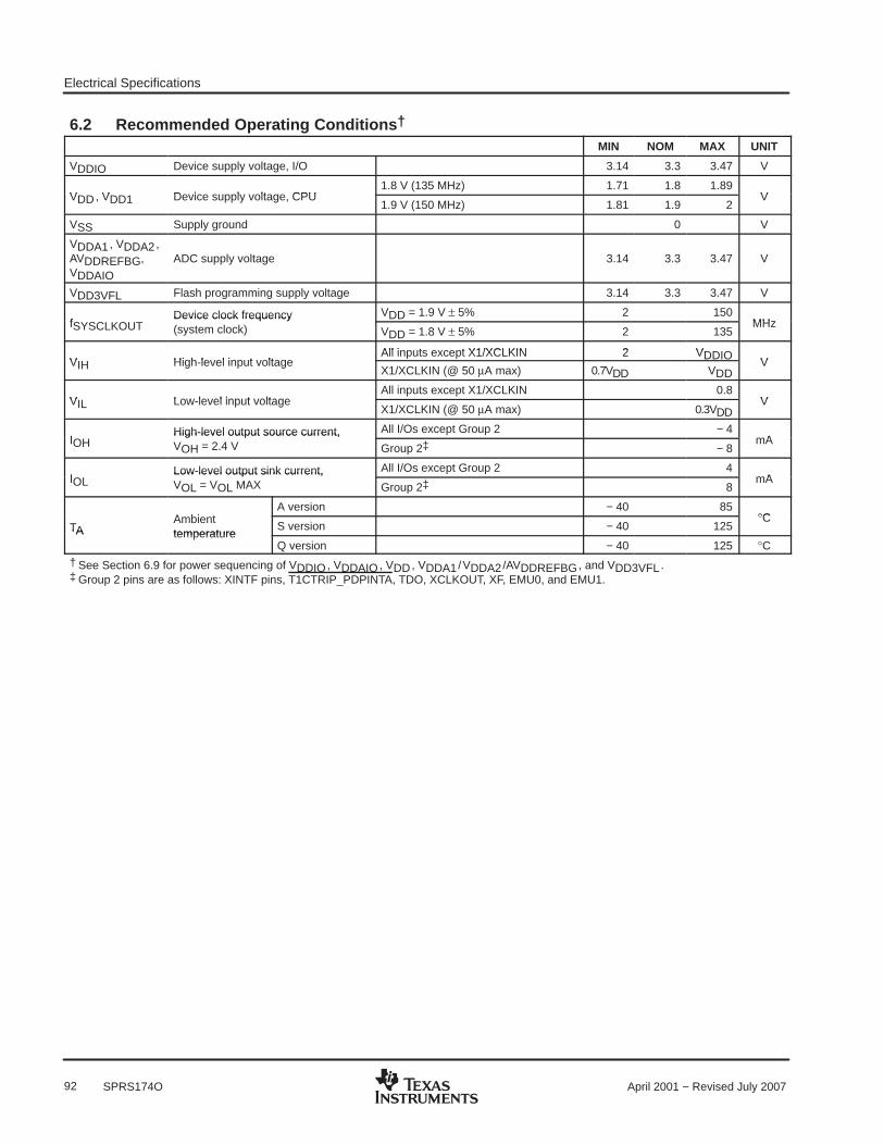
Electrical Specifications
92 April 2001 − Revised July 2007SPRS174O
6.2 Recommended Operating Conditions † MIN NOM MAX UNIT
VDDIO Device supply voltage, I/O 3.14 3.3 3.47 V
VDD, VDD1 Device supply voltage, CPU1.8 V (135 MHz) 1.71 1.8 1.89
VVDD, VDD1 Device supply voltage, CPU1.9 V (150 MHz) 1.81 1.9 2
V
VSS Supply ground 0 V
VDDA1, VDDA2,AVDDREFBG,VDDAIO
ADC supply voltage 3.14 3.3 3.47 V
VDD3VFL Flash programming supply voltage 3.14 3.3 3.47 V
fSYSCLKOUTDevice clock frequency VDD = 1.9 V ± 5% 2 150
MHzfSYSCLKOUTDevice clock frequency(system clock) VDD = 1.8 V ± 5% 2 135
MHz
All inputs except X1/XCLKIN 2 VDDIOVIH High-level input voltage
All inputs except X1/XCLKIN 2 VDDIOVVIH High-level input voltage
X1/XCLKIN (@ 50 µA max) 0.7VDD VDDV
VIL Low-level input voltageAll inputs except X1/XCLKIN 0.8
VVIL Low-level input voltageX1/XCLKIN (@ 50 µA max) 0.3VDD
V
IOHHigh-level output source current, All I/Os except Group 2 − 4
mAIOHHigh-level output source current,VOH = 2.4 V Group 2‡ − 8
mA
IOLLow-level output sink current, All I/Os except Group 2 4
mAIOLLow-level output sink current,VOL = VOL MAX Group 2‡ 8
mA
Ambient A version − 40 85
°CTA
Ambient temperature
S version − 40 125°C
TA temperatureQ version − 40 125 °C
† See Section 6.9 for power sequencing of VDDIO, VDDAIO, VDD, VDDA1/VDDA2/AVDDREFBG, and VDD3VFL.‡ Group 2 pins are as follows: XINTF pins, T1CTRIP_PDPINTA, TDO, XCLKOUT, XF, EMU0, and EMU1.
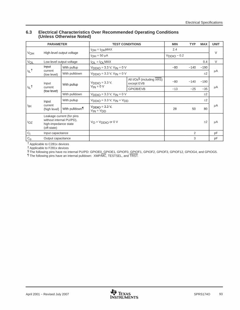
Electrical Specifications
93April 2001 − Revised July 2007 SPRS174O
6.3 Electrical Characteristics Over Recommended Operating Conditions(Unless Otherwise Noted)
PARAMETER TEST CONDITIONS MIN TYP MAX UNIT
VOH High-level output voltageIOH = IOHMAX 2.4
VVOH High-level output voltageIOH = 50 µA VDDIO − 0.2
V
VOL Low-level output voltage IOL = IOLMAX 0.4 VVOL Low-level output voltage IOL = IOLMAX 0.4 V
Input With pullup VDDIO = 3.3 V, VIN = 0 V −80 −140 −190IIL†
Inputcurrent
With pullup VDDIO = 3.3 V, VIN = 0 V −80 −140 −190AIIL† current
(low level) With pulldown VDDIO = 3.3 V, VIN = 0 V ±2µA
IIL‡Inputcurrent
With pullupVDDIO = 3.3 V,VIN = 0 V
All I/Os§ (including XRS)except EVB
−80 −140 −190
AIIL‡Inputcurrent(low level)
With pullup DDIOVIN = 0 V
GPIOB/EVB −13 −25 −35µA
(low level)With pulldown VDDIO = 3.3 V, VIN = 0 V ±2
Inputcurrent
With pullup VDDIO = 3.3 V, VIN = VDD ±2
IIH
Inputcurrent(high level) With pulldown¶ VDDIO = 3.3 V,
28 50 80µAIIH current
(high level) With pulldown¶ VDDIO = 3.3 V,VIN = VDD
28 50 80µA
IOZ
Leakage current (for pinswithout internal PU/PD),high-impedance state(off-state)
VO = VDDIO or 0 V ±2 µA
Ci Input capacitance 2 pF
Co Output capacitance 3 pF
† Applicable to C281x devices‡ Applicable to F281x devices§ The following pins have no internal PU/PD: GPIOE0, GPIOE1, GPIOF0, GPIOF1, GPIOF2, GPIOF3, GPIOF12, GPIOG4, and GPIOG5.¶ The following pins have an internal pulldown: XMP/MC, TESTSEL, and TRST.

Electrical Specifications
94 April 2001 − Revised July 2007SPRS174O
6.4 Current Consumption by Power-Supply Pins Over Recommended Operating ConditionsDuring Low-Power Modes at 150-MHz SYSCLKOUT (TMS320F281x)
MODE TEST CONDITIONSIDD IDDIO† IDD3VFL IDDA‡
MODE TEST CONDITIONSTYP MAX§ TYP MAX§ TYP MAX§ TYP MAX§
Operational
All peripheral clocks are enabled. AllPWM pins are toggled at 100 kHz.Data is continuously transmitted out ofthe SCIA, SCIB, and CAN ports. Thehardware multiplier is exercised.Code is running out of flash with 5wait-states.
195 mA¶ 230 mA 15 mA 30 mA 40 mA 45 mA 40 mA 50 mA
IDLE
− Flash is powered down− XCLKOUT is turned off− All peripheral clocks are on,
except ADC
125 mA 150 mA 5 mA 10 mA 2 µA 4 µA 1 µA 20 µA
STANDBY
− Flash is powered down− Peripheral clocks are turned off− Pins without an internal PU/PD
are tied high/low
5 mA 10 mA 5 µA 20 µA 2 µA 4 µA 1 µA 20 µA
HALT
− Flash is powered down− Peripheral clocks are turned off− Pins without an internal PU/PD
are tied high/low− Input clock is disabled
70 µA 5 µA 20 µA 2 µA 4 µA 1 µA 20 µA
† IDDIO current is dependent on the electrical loading on the I/O pins.‡ IDDA includes current into VDDA1, VDDA2, AVDDREFBG, and VDDAIO pins.§ MAX numbers are at 125°C, and MAX voltage (VDD = 2.0 V; VDDIO, VDD3VFL, VDDA = 3.6 V).¶ IDD represents the total current drawn from the 1.8-V rail (VDD). It includes a small amount of current (<1 mA) drawn by VDD1.
NOTE:HALT and STANDBY modes cannot be used when the PLL is disabled.
6.5 Current Consumption by Power-Supply Pins Over Recommended Operating ConditionsDuring Low-Power Modes at 150-MHz SYSCLKOUT (TMS320C281x)
MODE TEST CONDITIONSIDD IDDIO† IDDA‡
MODE TEST CONDITIONSTYP MAX§ TYP MAX§ TYP MAX§
Operational
All peripheral clocks are enabled. All PWM pins aretoggled at 100 kHz.Data is continuously transmitted out of the SCIA, SCIB,and CAN ports. The hardware multiplier is exercised.Code is running out of ROM with 5 wait-states.
210 mA¶ 260 mA 20 mA 30 mA 40 mA 50 mA
IDLE− XCLKOUT is turned off− All peripheral clocks are on, except ADC
140 mA 165 mA 20 mA 30 mA 5 µA 10 µA
STANDBY− Peripheral clocks are turned off− Pins without an internal PU/PD are tied high/low
5 mA 10mA 5 µA 20 µA 5 µA 10 µA
HALT− Peripheral clocks are turned off− Pins without an internal PU/PD are tied high/low− Input clock is disabled
70 µA 5 µA 10 µA 1 µA
† IDDIO current is dependent on the electrical loading on the I/O pins.‡ IDDA includes current into VDDA1, VDDA2, AVDDREFBG, and VDDAIO pins.§ MAX numbers are at 125°C, and MAX voltage (VDD = 2.0 V; VDDIO, VDD3VFL, VDDA = 3.6 V).¶ IDD represents the total current drawn from the 1.8-V rail (VDD). It includes a small amount of current (<1 mA) drawn by VDD1.

Electrical Specifications
95April 2001 − Revised July 2007 SPRS174O
6.6 Current Consumption Graphs
0
50
100
150
200
250
0 20 40 60 80 100 120 140 160
SYSCLKOUT (MHz)
IDD IDDIO IDD3VFL IDDA Total 3.3−V current
Cur
rent
(m
A)
NOTES: A. Test conditions are as defined in Table 6−5 for operational currents.B. IDD represents the total current drawn from the 1.8-V rail (VDD). It includes a small amount of current (<1 mA) drawn by VDD1.C. IDDA represents the current drawn by VDDA1 and VDDA2 rails.D. Total 3.3-V current is the sum of IDDIO, IDD3VFL, and IDDA. It includes a small amount of current (<1 mA) drawn by VDDAIO.
.
Figure 6−1. F2812/F2811/F2810 Typical Current Consumption Over Frequency
0
100
200
300
400
500
600
700
0 20 40 60 80 100 120 140 160
SYSCLKOUT (MHz)
Total Power
Pow
er (
mW
)
Figure 6−2. F2812/F2811/F2810 Typical Power Consumption Over Frequency

Electrical Specifications
96 April 2001 − Revised July 2007SPRS174O
0
50
100
150
200
250
0 20 40 60 80 100 120 140 160SYSCLKOUT (MHz)
IDD IDDIO IDDA Total 3.3−V current
Cur
rent
(m
A)
NOTES: A. Test conditions are as defined in Table 6−5 for operational currents.B. IDD represents the total current drawn from the 1.8-V rail (VDD). It includes a small amount of current (<1 mA) drawn
by VDD1.C. IDDA represents the current drawn by VDDA1 and VDDA2 rails.D. Total 3.3-V current is the sum of IDDIO and IDDA. It includes a small amount of current (<1 mA) drawn by VDDAIO.
Figure 6−3. C2812/C2811/C2810 Typical Current Consumption Over Frequency
0
100
200
300
400
500
600
0 20 40 60 80 100 120 140 160
Total PowerSYSCLKOUT (MHz)
Pow
er (
mW
)
Figure 6−4. C2812/C2811/C2810 Typical Power Consumption Over Frequency

Electrical Specifications
97April 2001 − Revised July 2007 SPRS174O
6.7 Reducing Current Consumption
28x DSPs incorporate a unique method to reduce the device current consumption. A reduction in currentconsumption can be achieved by turning off the clock to any peripheral module which is not used in a givenapplication. Table 6−1 indicates the typical reduction in current consumption achieved by turning off the clocksto various peripherals.
Table 6−1. Typical Current Consumption by Various Peripherals (at 150 MHz) †
PERIPHERAL MODULE IDD CURRENT REDUCTION (mA)
eCAN 12
EVA 6
EVB 6
ADC 8‡
SCI 4
SPI 5
McBSP 13
† All peripheral clocks are disabled upon reset. Writing to/reading from peripheral registers is possible only after the peripheral clocks are turnedon.
‡ This number represents the current drawn by the digital portion of the ADC module. Turning off the clock to the ADC module results in theelimination of the current drawn by the analog portion of the ADC (IDDA) as well.
6.8 Emulator Connection Without Signal Buffering for the DSP
Figure 6−3 shows the connection between the DSP and JTAG header for a single-processor configuration.If the distance between the JTAG header and the DSP is greater than 6 inches, the emulation signals mustbe buffered. If the distance is less than 6 inches, buffering is typically not needed. Figure 6−3 shows thesimpler, no-buffering situation. For the pullup/pulldown resistor values, see the pin description section.

Electrical Specifications
98 April 2001 − Revised July 2007SPRS174O
EMU0
EMU1
TMS
TDI
TDO
TCK
VDDIO
DSP
EMU0
EMU1
TMS
TDI
TDO
TCK
TCK_RET
13
14
2
1
3
7
11
9
6 inches or less
PD
GND
GND
GND
GND
GND
5
4
6
8
10
12
JTAG Header
VDDIO
TRSTTRST
Figure 6−5. Emulator Connection Without Signal Buffering for the DSP
6.9 Power Sequencing Requirements
TMS320F2812/F2811/F2810 silicon requires dual voltages (1.8-V or 1.9-V and 3.3-V) to power up the CPU,Flash, ROM, ADC, and the I/Os. To ensure the correct reset state for all modules during power up, there aresome requirements to be met while powering up/powering down the device. The current F2812 siliconreference schematics (Spectrum Digital Incorporated eZdsp. board) suggests two options for the powersequencing circuit.
Power sequencing is not needed for C281x devices. In other words, 3.3-V and 1.8-V (or 1.9-V) can ramptogether. C281x can also be used on boards that have F281x power sequencing implemented; however, ifthe 1.8-V (or 1.9-V) rail lags the 3.3-V rail, the GPIO pins are undefined until the 1.8-V rail reaches at least1 V.
• Option 1:
In this approach, an external power sequencing circuit enables VDDIO first, then VDD and VDD1 (1.8 V or1.9 V). After 1.8 V (or 1.9 V) ramps, the 3.3 V for Flash (VDD3VFL) and ADC (VDDA1/VDDA2/AVDDREFBG)modules are ramped up. While option 1 is still valid, TI has simplified the requirement. Option 2 is therecommended approach.
• Option 2:
Enable power to all 3.3-V supply pins (VDDIO, VDD3VFL, VDDA1/VDDA2/VDDAIO/AVDDREFBG) and thenramp 1.8 V (or 1.9 V) (VDD/VDD1) supply pins.
1.8 V or 1.9 V (VDD/VDD1) should not reach 0.3 V until VDDIO has reached 2.5 V. This ensures the resetsignal from the I/O pin has propagated through the I/O buffer to provide power-on reset to all the modulesinside the device. See Figure 6−11 for power-on reset timing.
• Power-Down Sequencing:
During power-down, the device reset should be asserted low (8 µs, minimum) before the VDD supplyreaches 1.5 V. This will help to keep on-chip flash logic in reset prior to the VDDIO/VDD power suppliesramping down. It is recommended that the device reset control from “Low-Dropout (LDO)” regulators orvoltage supervisors be used to meet this constraint. LDO regulators that facilitate power-sequencing (with
eZdsp is a trademark of Spectrum Digital Incorporated.
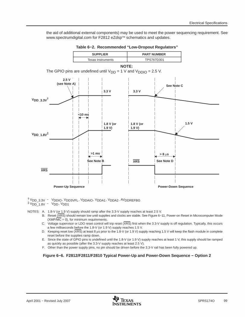
Electrical Specifications
99April 2001 − Revised July 2007 SPRS174O
the aid of additional external components) may be used to meet the power sequencing requirement. Seewww.spectrumdigital.com for F2812 eZdsp schematics and updates.
Table 6−2. Recommended “Low-Dropout Regulators”
SUPPLIER PART NUMBER
Texas Instruments TPS767D301
NOTE:The GPIO pins are undefined until VDD = 1 V and VDDIO = 2.5 V.
VDD_3.3V†
2.5 V(see Note A)
3.3 V
VDD_1.8V‡
XRS
1.8 V (or1.9 V)
XRS
> 8 µs
1.5 V
3.3 V
<10 ms
>1 ms
Power-Up Sequence Power-Down Sequence
1.8 V (or1.9 V)
† VDD_3.3V − VDDIO, VDD3VFL, VDDAIO, VDDA1, VDDA2, AVDDREFBG‡ VDD_1.8V − VDD, VDD1
NOTES: A. 1.8-V (or 1.9 V) supply should ramp after the 3.3-V supply reaches at least 2.5 V.B. Reset (XRS) should remain low until supplies and clocks are stable. See Figure 6−11, Power-on Reset in Microcomputer Mode
(XMP/MC = 0), for minimum requirements.C. Voltage supervisor or LDO reset control will trip reset (XRS) first when the 3.3-V supply is off regulation. Typically, this occurs
a few milliseconds before the 1.8-V (or 1.9 V) supply reaches 1.5 V.D. Keeping reset low (XRS) at least 8 µs prior to the 1.8-V (or 1.9 V) supply reaching 1.5 V will keep the flash module in complete
reset before the supplies ramp down.E. Since the state of GPIO pins is undefined until the 1.8-V (or 1.9 V) supply reaches at least 1 V, this supply should be ramped
as quickly as possible (after the 3.3-V supply reaches at least 2.5 V).F. Other than the power supply pins, no pin should be driven before the 3.3-V rail has been fully powered up.
See Note B See Note D
See Note C
Figure 6−6. F2812/F2811/F2810 Typical Power-Up and Power-Down Sequence − Option 2

Electrical Specifications
100 April 2001 − Revised July 2007SPRS174O
6.10 Signal Transition Levels
Note that some of the signals use different reference voltages, see the recommended operating conditionstable. Output levels are driven to a minimum logic-high level of 2.4 V and to a maximum logic-low level of 0.4 V.
Figure 6−7 shows output levels.
0.4 V (VOL)
2.4 V (VOH)
Figure 6−7. Output Levels
Output transition times are specified as follows:
• For a high-to-low transition, the level at which the output is said to be no longer high is below VOH(MIN)and the level at which the output is said to be low is VOL(MAX) and lower.
• For a low-to-high transition, the level at which the output is said to be no longer low is above VOL(MAX)and the level at which the output is said to be high is VOH(MIN) and higher.
Figure 6−8 shows the input levels.
0.8 V (VIL)
2.0 V (VIH)
Figure 6−8. Input Levels
Input transition times are specified as follows:
• For a high-to-low transition on an input signal, the level at which the input is said to be no longer high isbelow VIH(MIN) and the level at which the input is said to be low is VIL(MAX) and lower.
• For a low-to-high transition on an input signal, the level at which the input is said to be no longer low isabove VIL(MAX) and the level at which the input is said to be high is VIH(MIN) and higher.
NOTE: See the individual timing diagrams for levels used for testing timing parameters.

Electrical Specifications
101April 2001 − Revised July 2007 SPRS174O
6.11 Timing Parameter Symbology
Timing parameter symbols used are created in accordance with JEDEC Standard 100. To shorten thesymbols, some of the pin names and other related terminology have been abbreviated as follows:
Lowercase subscripts and their meanings: Letters and symbols and their meanings:
a access time H High
c cycle time (period) L Low
d delay time V Valid
f fall time X Unknown, changing, or don’t care level
h hold time Z High impedance
r rise time
su setup time
t transition time
v valid time
w pulse duration (width)
6.12 General Notes on Timing Parameters
All output signals from the 28x devices (including XCLKOUT) are derived from an internal clock such that alloutput transitions for a given half-cycle occur with a minimum of skewing relative to each other.
The signal combinations shown in the following timing diagrams may not necessarily represent actual cycles.For actual cycle examples, see the appropriate cycle description section of this document.
6.13 Test Load Circuit
This test load circuit is used to measure all switching characteristics provided in this document.
Transmission Line
4.0 pF 1.85 pF
Z0 = 50 Ω(see note)
Tester Pin Electronics Data Sheet Timing Reference Point
OutputUnderTest
NOTE: The data sheet provides timing at the device pin. For output timing analysis, the tester pin electronics and its transmission line effectsmust be taken into account. A transmission line with a delay of 2 ns or longer can be used to produce the desired transmission line effect.The transmission line is intended as a load only. It is not necessary to add or subtract the transmission line delay (2 ns or longer) fromthe data sheet timing.
42 Ω 3.5 nH
Device Pin(see note)
Input requirements in this data sheet are tested with an input slew rate of < 4 Volts per nanosecond (4 V/ns) at the device pin.
Figure 6−9. 3.3-V Test Load Circuit
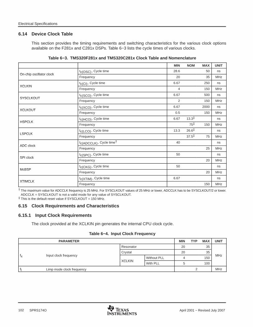
Electrical Specifications
102 April 2001 − Revised July 2007SPRS174O
6.14 Device Clock Table
This section provides the timing requirements and switching characteristics for the various clock optionsavailable on the F281x and C281x DSPs. Table 6−3 lists the cycle times of various clocks.
Table 6−3. TMS320F281x and TMS320C281x Clock Table and Nomenclature
MIN NOM MAX UNIT
On-chip oscillator clocktc(OSC) , Cycle time 28.6 50 ns
On-chip oscillator clockFrequency 20 35 MHz
XCLKINtc(CI) , Cycle time 6.67 250 ns
XCLKINFrequency 4 150 MHz
SYSCLKOUTtc(SCO) , Cycle time 6.67 500 ns
SYSCLKOUTFrequency 2 150 MHz
XCLKOUTtc(XCO) , Cycle time 6.67 2000 ns
XCLKOUTFrequency 0.5 150 MHz
HSPCLKtc(HCO) , Cycle time 6.67 13.3‡ ns
HSPCLKFrequency 75‡ 150 MHz
LSPCLKtc(LCO) , Cycle time 13.3 26.6‡ ns
LSPCLKFrequency 37.5‡ 75 MHz
ADC clocktc(ADCCLK) , Cycle time† 40 ns
ADC clockFrequency 25 MHz
SPI clocktc(SPC) , Cycle time 50 ns
SPI clockFrequency 20 MHz
McBSPtc(CKG) , Cycle time 50 ns
McBSPFrequency 20 MHz
XTIMCLKtc(XTIM) , Cycle time 6.67 ns
XTIMCLKFrequency 150 MHz
† The maximum value for ADCCLK frequency is 25 MHz. For SYSCLKOUT values of 25 MHz or lower, ADCCLK has to be SYSCLKOUT/2 or lower.ADCCLK = SYSCLKOUT is not a valid mode for any value of SYSCLKOUT.
‡ This is the default reset value if SYSCLKOUT = 150 MHz.
6.15 Clock Requirements and Characteristics
6.15.1 Input Clock Requirements
The clock provided at the XCLKIN pin generates the internal CPU clock cycle.
Table 6−4. Input Clock Frequency
PARAMETER MIN TYP MAX UNIT
Resonator 20 35
fx Input clock frequencyCrystal 20 35
MHzfx Input clock frequency
XCLKINWithout PLL 4 150
MHz
XCLKINWith PLL 5 100
fl Limp mode clock frequency 2 MHz

Electrical Specifications
103April 2001 − Revised July 2007 SPRS174O
Table 6−5. XCLKIN Timing Requirements − PLL Bypassed or Enabled
NO. MIN MAX UNIT
C8 tc(CI) Cycle time, XCLKIN 6.67 250 ns
C9 tf(CI) Fall time, XCLKIN 6 nsC9 tf(CI) Fall time, XCLKIN 6 ns
C10 tr(CI) Rise time, XCLKIN 6 nsC10 tr(CI) Rise time, XCLKIN 6 ns
C11 tw(CIL) Pulse duration, X1/XCLKIN low as a percentage of tc(CI) 40 60 %
C12 tw(CIH) Pulse duration, X1/XCLKIN high as a percentage of tc(CI) 40 60 %
Table 6−6. XCLKIN Timing Requirements − PLL Disabled
NO. MIN MAX UNIT
C8 tc(CI) Cycle time, XCLKIN 6.67 250 ns
C9 tf(CI) Fall time, XCLKINUp to 30 MHz 6
nsC9 tf(CI) Fall time, XCLKIN30 MHz to 150 MHz 2
ns
C10 tr(CI) Rise time, XCLKINUp to 30 MHz 6
nsC10 tr(CI) Rise time, XCLKIN30 MHz to 150 MHz 2
ns
C11 tw(CIL) Pulse duration, X1/XCLKIN low as a percentage of tc(CI)XCLKIN ≤ 120 MHz 40 60
%C11 tw(CIL) Pulse duration, X1/XCLKIN low as a percentage of tc(CI)120 < XCLKIN ≤ 150 MHz 45 55
%
C12 tw(CIH) Pulse duration, X1/XCLKIN high as a percentage of tc(CI)XCLKIN ≤ 120 MHz 40 60
%C12 tw(CIH) Pulse duration, X1/XCLKIN high as a percentage of tc(CI)120 < XCLKIN ≤ 150 MHz 45 55
%
Table 6−7. Possible PLL Configuration Modes
PLL MODE REMARKS SYSCLKOUT
PLL DisabledInvoked by tying XPLLDIS pin low upon reset. PLL block is completelydisabled. Clock input to the CPU (CLKIN) is directly derived from the clocksignal present at the X1/XCLKIN pin.
XCLKIN
PLL BypassedDefault PLL configuration upon power-up, if PLL is not disabled. The PLLitself is bypassed. However, the /2 module in the PLL block divides the clockinput at the X1/XCLKIN pin by two before feeding it to the CPU.
XCLKIN/2
PLL EnabledAchieved by writing a non-zero value “n” into PLLCR register. The /2 modulein the PLL block now divides the output of the PLL by two before feeding it tothe CPU.
(XCLKIN * n) / 2
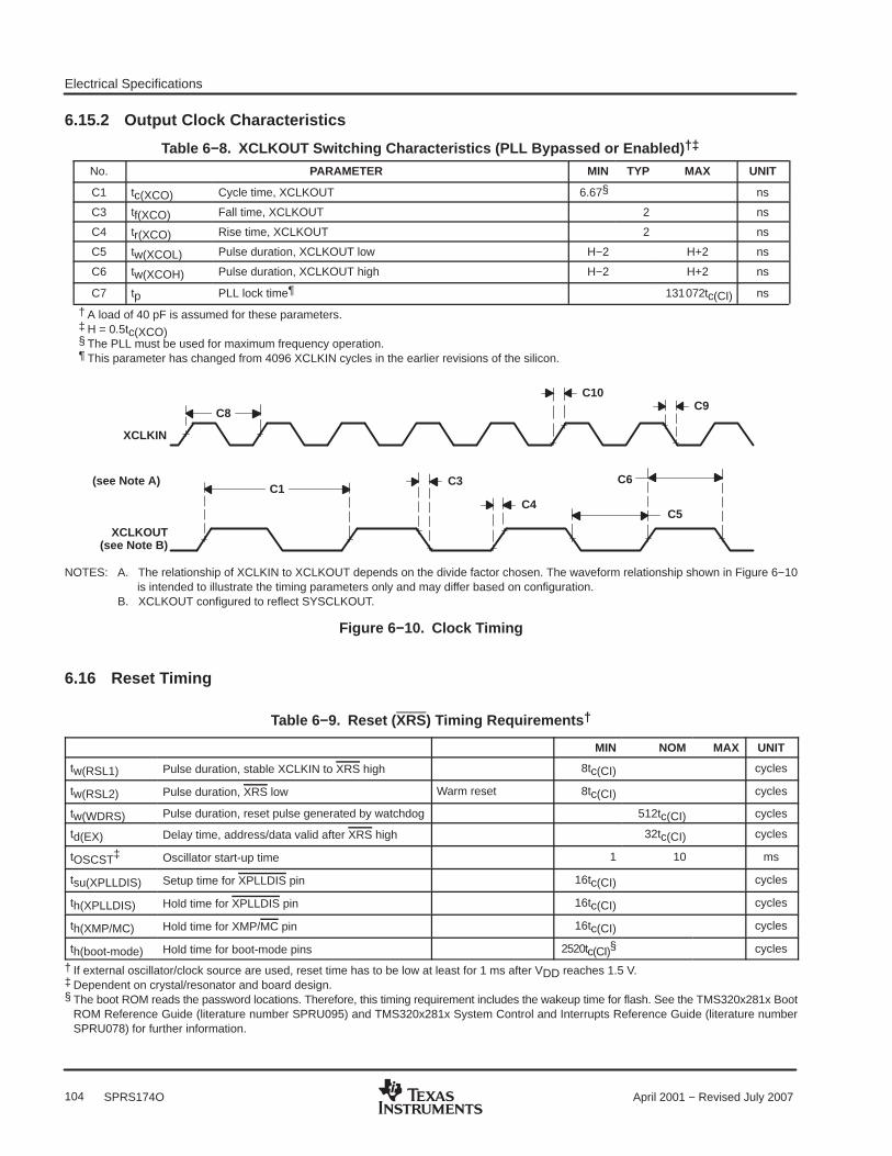
Electrical Specifications
104 April 2001 − Revised July 2007SPRS174O
6.15.2 Output Clock Characteristics
Table 6−8. XCLKOUT Switching Characteristics (PLL Bypassed or Enabled) †‡
No. PARAMETER MIN TYP MAX UNIT
C1 tc(XCO) Cycle time, XCLKOUT 6.67§ ns
C3 tf(XCO) Fall time, XCLKOUT 2 ns
C4 tr(XCO) Rise time, XCLKOUT 2 ns
C5 tw(XCOL) Pulse duration, XCLKOUT low H−2 H+2 ns
C6 tw(XCOH) Pulse duration, XCLKOUT high H−2 H+2 ns
C7 tp PLL lock time¶ 131072tc(CI) ns
† A load of 40 pF is assumed for these parameters.‡ H = 0.5tc(XCO)§ The PLL must be used for maximum frequency operation.¶ This parameter has changed from 4096 XCLKIN cycles in the earlier revisions of the silicon.
C4
C3
XCLKOUT(see Note B)
XCLKIN
C5
C9C10
C1
C8
C6(see Note A)
NOTES: A. The relationship of XCLKIN to XCLKOUT depends on the divide factor chosen. The waveform relationship shown in Figure 6−10is intended to illustrate the timing parameters only and may differ based on configuration.
B. XCLKOUT configured to reflect SYSCLKOUT.
Figure 6−10. Clock Timing
6.16 Reset Timing
Table 6−9. Reset (XRS ) Timing Requirements †
MIN NOM MAX UNIT
tw(RSL1) Pulse duration, stable XCLKIN to XRS high 8tc(CI) cycles
tw(RSL2) Pulse duration, XRS low Warm reset 8tc(CI) cycles
tw(WDRS) Pulse duration, reset pulse generated by watchdog 512tc(CI) cycles
td(EX) Delay time, address/data valid after XRS high 32tc(CI) cycles
tOSCST‡ Oscillator start-up time 1 10 ms
tsu(XPLLDIS) Setup time for XPLLDIS pin 16tc(CI) cycles
th(XPLLDIS) Hold time for XPLLDIS pin 16tc(CI) cycles
th(XMP/MC) Hold time for XMP/MC pin 16tc(CI) cycles
th(boot-mode) Hold time for boot-mode pins 2520tc(CI)§ cycles
† If external oscillator/clock source are used, reset time has to be low at least for 1 ms after VDD reaches 1.5 V.‡ Dependent on crystal/resonator and board design.§ The boot ROM reads the password locations. Therefore, this timing requirement includes the wakeup time for flash. See the TMS320x281x Boot
ROM Reference Guide (literature number SPRU095) and TMS320x281x System Control and Interrupts Reference Guide (literature numberSPRU078) for further information.

Electrical Specifications
105April 2001 − Revised July 2007 SPRS174O
tw(RSL1)
th(XPLLDIS)
th(XMP/MC)
th(boot-mode) (C)
VDDIO, VDD3VFLVDDAn (A), VDDAIO
(3.3 V)
XCLKIN
2.5 V
0.3 V
X1
XRS
XF/XPLLDIS
XMP/MC
Boot-Mode Pins
VDD, VDD1(1.8 V (or 1.9 V))
XCLKOUT
I/O Pins
User-Code Dependent
User-Code Dependent
User-Code Dependent
Boot-ROM Execution StartsPeripheral/GPIO FunctionBased on Boot Code
GPIO Pins as Input
XPLLDIS Sampling
GPIOF14
XCLKIN/8(B)
GPIO Pins as Input (State Depends on Internal PU/PD)
tOSCST
(Don’t Care)
(Don’t Care)
User-Code Dependent
Address/Data/Control
Address/Data Valid. Internal Boot-ROM Code Execution Phase
User-Code Execution Phase
NOTES: A. VDDAn − VDDA1/VDDA2 and AVDDREFBGB. Upon power up, SYSCLKOUT is XCLKIN/2 if the PLL is enabled. Since both the XTIMCLK and CLKMODE bits in the
XINTCNF2 register come up with a reset state of 1, SYSCLKOUT is further divided by 4 before it appears at XCLKOUT.This explains why XCLKOUT = XCLKIN/8 during this phase.
C. After reset, the Boot ROM code executes instructions for 1260 SYSCLKOUT cycles (SYSCLKOUT = XCLKIN/2) and thensamples BOOT Mode pins. Based on the status of the Boot Mode pin, the boot code branches to destination memory orboot code function in ROM. The BOOT Mode pins should be held high/low for at least 2520 XCLKIN cycles from boot ROMexecution time for proper selection of Boot modes.If Boot ROM code executes after power-on conditions (in debugger environment), the Boot code execution time is basedon the current SYSCLKOUT speed. The SYSCLKOUT will be based on user environment and could be with or without PLLenabled.
D. The state of the GPIO pins is undefined (i.e., they could be input or output) until the 1.8-V (or 1.9-V) supply reaches at least1 V and 3.3-V supply reaches 2.5 V.
td(EX)
(D)
tsu(XPLLDIS)
Figure 6−11. Power-on Reset in Microcomputer Mode (XMP/MC = 0) (See Note D)

Electrical Specifications
106 April 2001 − Revised July 2007SPRS174O
tw(RSL)
th(XPLLDIS)
th(XMP/MC)
tOSCST
VDDIO, VDD3VFLVDDAn, VDDAIO
(3.3 V)
XCLKIN
X1
XRS
XF/XPLLDIS
XMP/MC
VDD, VDD1 (1.8 V (or1.9 V))
I/O Pins
XPLLDIS Sampling
Address/Data/Control
XCLKOUT
(Don’t Care)
(Don’t Care)
GPIOF14/XF (User-Code Dependent)
XCLKIN/8 (See Note A)
(Don’t Care)
Input Configuration (State Depends on Internal PU/PD)
User-Code Dependent
Address/Data/Control Valid ExecutionBegins From External Boot Address 0x3FFFC0
User-Code Dependent
2.5 V
0.3 V
td(EX)
NOTES: A. Upon power up, SYSCLKOUT is XCLKIN/2 if the PLL is enabled. Since both the XTIMCLK and CLKMODE bits in the XINTCNF2register come up with a reset state of 1, SYSCLKOUT is further divided by 4 before it appears at XCLKOUT. This explains whyXCLKOUT = XCLKIN/8 during this phase.
B. The state of the GPIO pins is undefined (i.e., they could be input or output) until the 1.8-V (or 1.9-V) supply reaches at least 1 Vand 3.3-V supply reaches 2.5 V..
See Note B
tsu(XPLLDIS)
Figure 6−12. Power-on Reset in Microprocessor Mode (XMP/MC = 1)

Electrical Specifications
107April 2001 − Revised July 2007 SPRS174O
XCLKIN/8
(XCLKIN * 5)
th(XPLLDIS)
th(XMP/MC)
th(boot-mode) †
tw(RSL2)
XCLKIN
X1
XRS
XF/XPLLDIS
XMP/MC
Boot-Mode Pins
XCLKOUT
I/O Pins
Address/Data/Control
Boot-ROM Execution Starts
User-Code Execution Starts
User-Code Dependent
User-Code Dependent
User-Code Execution Phase
(Don’t Care)
(Don’t Care)
(Don’t Care)(Don’t Care)
User-Code Dependent
User-Code Execution
Peripheral/GPIO Function
User-Code Dependent
GPIO Pins as Input (State Depends on Internal PU/PD)
GPIO Pins as Input
GPIOF14/XF
XPLLDIS Sampling
GPIOF14
Peripheral/GPIO Function
† After reset, the Boot ROM code executes instructions for 1260 SYSCLKOUT cycles (SYSCLKOUT = XCLKIN/2) and then samples BOOTMode pins. Based on the status of the Boot Mode pin, the boot code branches to destination memory or boot code function in ROM. TheBOOT Mode pins should be held high/low for at least 2520 XCLKIN cycles from boot ROM execution time for proper selection of Bootmodes.If Boot ROM code executes after power-on conditions (in debugger environment), the Boot code execution time is based on the currentSYSCLKOUT speed. The SYSCLKOUT will be based on user environment and could be with or without PLL enabled.
td(EX)
tsu(XPLLDIS)
Figure 6−13. Warm Reset in Microcomputer Mode
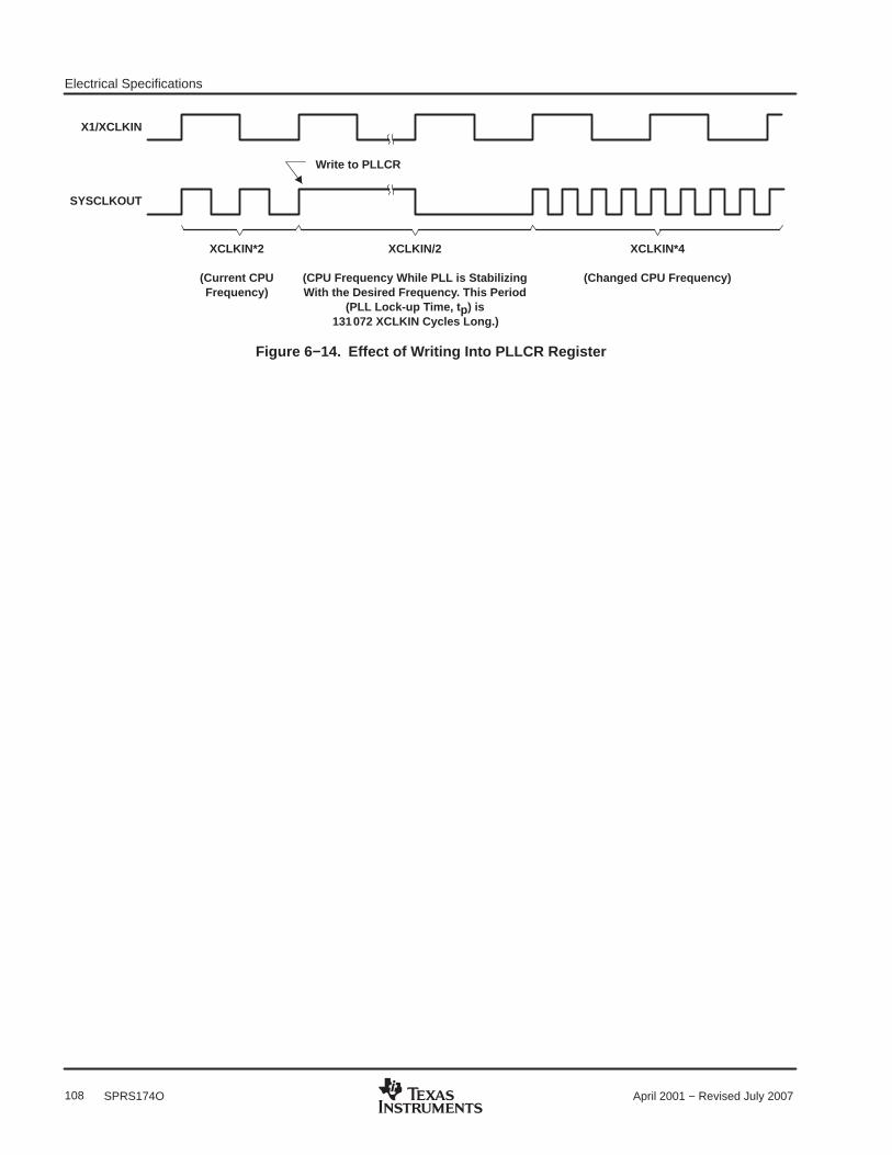
Electrical Specifications
108 April 2001 − Revised July 2007SPRS174O
X1/XCLKIN
SYSCLKOUT
Write to PLLCR
XCLKIN*2
(Current CPUFrequency)
XCLKIN/2
(CPU Frequency While PLL is StabilizingWith the Desired Frequency. This Period
(PLL Lock-up Time, t p) is131072 XCLKIN Cycles Long.)
XCLKIN*4
(Changed CPU Frequency)
Figure 6−14. Effect of Writing Into PLLCR Register
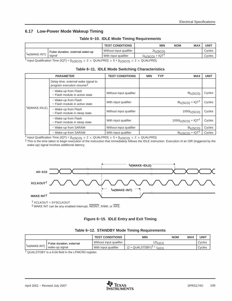
Electrical Specifications
109April 2001 − Revised July 2007 SPRS174O
6.17 Low-Power Mode Wakeup Timing
Table 6−10. IDLE Mode Timing Requirements
TEST CONDITIONS MIN NOM MAX UNIT
tw(WAKE-INT)Pulse duration, external wake-up Without input qualifier 2tc(SCO) Cycles
tw(WAKE-INT)Pulse duration, external wake-upsignal With input qualifier 1tc(SCO) + IQT† Cycles
† Input Qualification Time (IQT) = [tc(SCO) 2 QUALPRD] 5 + [tc(SCO) 2 QUALPRD].
Table 6−11. IDLE Mode Switching Characteristics
PARAMETER TEST CONDITIONS MIN TYP MAX UNIT
Delay time, external wake signal toprogram execution resume‡
− Wake-up from Flash − Flash module in active state
Without input qualifier 8tc(SCO) Cycles
td(WAKE-IDLE)
− Wake-up from Flash − Flash module in active state
With input qualifier 8tc(SCO) + IQT† Cycles
td(WAKE-IDLE) − Wake-up from Flash − Flash module in sleep state
Without input qualifier 1050tc(SCO) Cycles
− Wake-up from Flash − Flash module in sleep state
With input qualifier 1050tc(SCO) + IQT† Cycles
− Wake-up from SARAM Without input qualifier 8tc(SCO) Cycles
− Wake-up from SARAM With input qualifier 8tc(SCO) + IQT† Cycles† Input Qualification Time (IQT) = [tc(SCO) 2 QUALPRD] 5 + [tc(SCO) 2 QUALPRD].‡ This is the time taken to begin execution of the instruction that immediately follows the IDLE instruction. Execution of an ISR (triggered by the
wake-up) signal involves additional latency.
WAKE INT‡
XCLKOUT†
A0−A15
td(WAKE−IDLE)
† XCLKOUT = SYSCLKOUT‡ WAKE INT can be any enabled interrupt, WDINT, XNMI, or XRS.
tw(WAKE−INT)
Figure 6−15. IDLE Entry and Exit Timing
Table 6−12. STANDBY Mode Timing Requirements
TEST CONDITIONS MIN NOM MAX UNIT
tw(WAKE-INT)Pulse duration, external Without input qualifier 12tc(CI) Cycles
tw(WAKE-INT)Pulse duration, externalwake-up signal With input qualifier (2 + QUALSTDBY)† * tc(CI) Cycles
† QUALSTDBY is a 6-bit field in the LPMCR0 register.

Electrical Specifications
110 April 2001 − Revised July 2007SPRS174O
Table 6−13. STANDBY Mode Switching Characteristics
PARAMETER TEST CONDITIONS MIN TYP MAX UNIT
td(IDLE-XCOH)Delay time, IDLE instructionexecuted to XCLKOUT high
32tc(SCO) 45tc(SCO) Cycles
Delay time, external wakesignal to program executionresume†
− Wake-up from Flash − Flash module in activestate
Without inputqualifier
12tc(CI) Cycles
td(WAKE-STBY)
− Wake-up from Flash − Flash module in activestate
With input qualifier 12tc(CI) + tw(WAKE-INT) Cyclestd(WAKE-STBY)
− Wake-up from Flash − Flash module in sleep state
Without inputqualifier
1125tc(SCO) Cycles
− Wake-up from Flash − Flash module in sleep state
With input qualifier 1125tc(SCO) + tw(WAKE-INT) Cycles
− Wake-up from SARAMWithout inputqualifier
12tc(CI) Cycles
− Wake-up from SARAM With input qualifier 12 tc(CI) + tw(WAKE-INT) Cycles
† This is the time taken to begin execution of the instruction that immediately follows the IDLE instruction. Execution of an ISR (triggered by thewake-up) signal involves additional latency.
tw(WAKE-INT)
td(WAKE-STBY)
td(IDLE−XCOH)
32 SYSCLKOUT Cycles
Wake-upSignal
X1/XCLKIN
XCLKOUT†
STANDBY Normal ExecutionSTANDBY
Flushing Pipeline
AB
CD
EF
DeviceStatus
NOTES: A. IDLE instruction is executed to put the device into STANDBY mode.B. The PLL block responds to the STANDBY signal. SYSCLKOUT is held for approximately 32 cycles before being turned
off. This 32-cycle delay enables the CPU pipe and any other pending operations to flush properly.C. Clocks to the peripherals are turned off. However, the PLL and watchdog are not shut down. The device is now in
STANDBY mode.D. The external wake-up signal is driven active (negative edge triggered shown as an example).E. After a latency period, the STANDBY mode is exited.F. Normal operation resumes. The device will respond to the interrupt (if enabled).
Figure 6−16. STANDBY Entry and Exit Timing
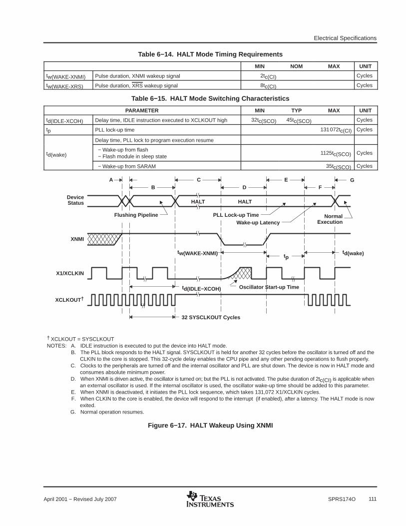
Electrical Specifications
111April 2001 − Revised July 2007 SPRS174O
Table 6−14. HALT Mode Timing Requirements
MIN NOM MAX UNIT
tw(WAKE-XNMI) Pulse duration, XNMI wakeup signal 2tc(CI) Cycles
tw(WAKE-XRS) Pulse duration, XRS wakeup signal 8tc(CI) Cycles
Table 6−15. HALT Mode Switching Characteristics
PARAMETER MIN TYP MAX UNIT
td(IDLE-XCOH) Delay time, IDLE instruction executed to XCLKOUT high 32tc(SCO) 45tc(SCO) Cycles
tp PLL lock-up time 131072tc(CI) Cycles
Delay time, PLL lock to program execution resume
td(wake) − Wake-up from flash − Flash module in sleep state
1125tc(SCO) Cycles
− Wake-up from SARAM 35tc(SCO) Cycles
† XCLKOUT = SYSCLKOUTNOTES: A. IDLE instruction is executed to put the device into HALT mode.
B. The PLL block responds to the HALT signal. SYSCLKOUT is held for another 32 cycles before the oscillator is turned off and theCLKIN to the core is stopped. This 32-cycle delay enables the CPU pipe and any other pending operations to flush properly.
C. Clocks to the peripherals are turned off and the internal oscillator and PLL are shut down. The device is now in HALT mode andconsumes absolute minimum power.
D. When XNMI is driven active, the oscillator is turned on; but the PLL is not activated. The pulse duration of 2tc(CI) is applicable whenan external oscillator is used. If the internal oscillator is used, the oscillator wake-up time should be added to this parameter.
E. When XNMI is deactivated, it initiates the PLL lock sequence, which takes 131,072 X1/XCLKIN cycles.F. When CLKIN to the core is enabled, the device will respond to the interrupt (if enabled), after a latency. The HALT mode is now
exited.G. Normal operation resumes.
td(IDLE−XCOH)
32 SYSCLKOUT Cycles
X1/XCLKIN
XCLKOUT†
HALT HALT
Wake-up LatencyFlushing Pipeline
td(wake)
AB
CD
DeviceStatus
E GF
PLL Lock-up Time
XNMI
NormalExecution
tw(WAKE-XNMI) tp
Oscillator Start-up Time
Figure 6−17. HALT Wakeup Using XNMI

Electrical Specifications
112 April 2001 − Revised July 2007SPRS174O
6.18 Event Manager Interface
6.18.1 PWM Timing
PWM refers to all PWM outputs on EVA and EVB.
Table 6−16. PWM Switching Characteristics †‡
PARAMETER TEST CONDITIONS MIN MAX UNIT
tw(PWM)§ Pulse duration, PWMx output high/low 25 ns
td(PWM)XCO Delay time, XCLKOUT high to PWMx output switching XCLKOUT = SYSCLKOUT/4 10 ns
† See the GPIO output timing for fall/rise times for PWM pins.‡ PWM pin toggling frequency is limited by the GPIO output buffer switching frequency (20 MHz).§ PWM outputs may be 100%, 0%, or increments of tc(HCO) with respect to the PWM period.
Table 6−17. Timer and Capture Unit Timing Requirements ¶#
MIN MAX UNIT
tw(TDIR) Pulse duration, TDIRx low/highWithout input qualifier 2tc(SCO)
cyclestw(TDIR) Pulse duration, TDIRx low/highWith input qualifier 1tc(SCO) + IQT|| cycles
tw(CAP) Pulse duration, CAPx input low/highWithout input qualifier 2tc(SCO)
cyclestw(CAP) Pulse duration, CAPx input low/highWith input qualifier 1tc(SCO) + IQT|| cycles
tw(TCLKINL) Pulse duration, TCLKINx low as a percentage of TCLKINx cycle time 40 60 %
tw(TCLKINH) Pulse duration, TCLKINx high as a percentage of TCLKINx cycle time 40 60 %
tc(TCLKIN) Cycle time, TCLKINx 4tc(HCO) ns¶ The QUALPRD bit field value can range from 0 (no qualification) through 0xFF (510 SYSCLKOUT cycles). The qualification sampling period is
2n SYSCLKOUT cycles, where “n” is the value stored in the QUALPRD bit field. As an example, when QUALPRD = 1, the qualification samplingperiod is 1 x 2 = 2 SYSCLKOUT cycles (i.e., the input is sampled every 2 SYSCLKOUT cycles). Six such samples will be taken over five samplingwindows, each window being 2n SYSCLKOUT cycles. For QUALPRD = 1, the minimum width that is needed is 5 x 2 = 10 SYSCLKOUT cycles.However, since the external signal is driven asynchronously, a 11-SYSCLKOUT-wide pulse ensures reliable recognition.
# Maximum input frequency to the QEP = min[HSPCLK/2, 20 MHz]|| Input Qualification Time (IQT) = [tc(SCO) 2 QUALPRD] 5 + [tc(SCO) 2 QUALPRD].
tw(PWM)
td(PWM)XCO
PWMx
XCLKOUT†
† XCLKOUT = SYSCLKOUT
Figure 6−18. PWM Output Timing
XCLKOUT†
tw(TDIR)
TDIRx
† XCLKOUT = SYSCLKOUT
Figure 6−19. TDIRx Timing
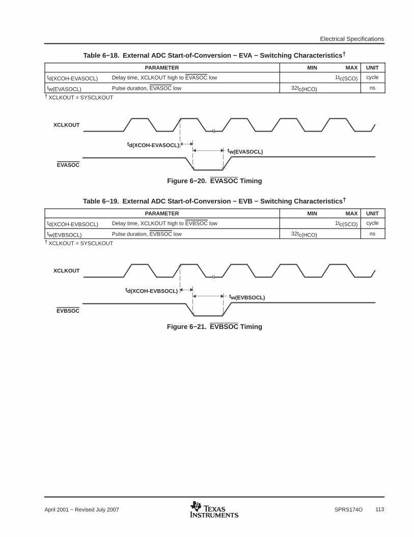
Electrical Specifications
113April 2001 − Revised July 2007 SPRS174O
Table 6−18. External ADC Start-of-Conversion − EVA − Switching Characteristics †
PARAMETER MIN MAX UNIT
td(XCOH-EVASOCL) Delay time, XCLKOUT high to EVASOC low 1tc(SCO) cycle
tw(EVASOCL) Pulse duration, EVASOC low 32tc(HCO) ns
† XCLKOUT = SYSCLKOUT
XCLKOUT
td(XCOH-EVASOCL)
EVASOC
tw(EVASOCL)
Figure 6−20. EVASOC Timing
Table 6−19. External ADC Start-of-Conversion − EVB − Switching Characteristics †
PARAMETER MIN MAX UNIT
td(XCOH-EVBSOCL) Delay time, XCLKOUT high to EVBSOC low 1tc(SCO) cycle
tw(EVBSOCL) Pulse duration, EVBSOC low 32tc(HCO) ns
† XCLKOUT = SYSCLKOUT
XCLKOUT
td(XCOH-EVBSOCL)
EVBSOC
tw(EVBSOCL)
Figure 6−21. EVBSOC Timing

Electrical Specifications
114 April 2001 − Revised July 2007SPRS174O
6.18.2 Interrupt Timing
Table 6−20. Interrupt Switching Characteristics
PARAMETER MIN MAX UNIT
td(PDP-PWM)HZDelay time, PDPINTx low to PWMhigh-impedance state
Without inputqualifier
12nstd(PDP-PWM)HZ high-impedance state
With input qualifier 1tc(SCO) + IQT† + 12
ns
td(TRIP-PWM)HZ
Delay time, CxTRIP/TxCTRIPsignals low to PWM
Without inputqualifier
3 * tc(SCO)nstd(TRIP-PWM)HZ signals low to PWM
high-impedance state With input qualifier 2tc(SCO) + IQT†ns
td(INT) Delay time, INT low/high to interrupt-vector fetch IQT + 12tc(SCO) ns
† Input Qualification Time (IQT) = [tc(SCO) 2 QUALPRD] 5 + [tc(SCO) 2 QUALPRD].
Table 6−21. Interrupt Timing Requirements
MIN MAX UNIT
tw(INT) Pulse duration, INT input low/highwith no qualifier 2tc(SCO)
cyclestw(INT) Pulse duration, INT input low/highwith qualifier 1tc(SCO) + IQT†
cycles
tw(PDP) Pulse duration, PDPINTx input lowwith no qualifier 2tc(SCO)
cyclestw(PDP) Pulse duration, PDPINTx input lowwith qualifier 1tc(SCO) + IQT†
cycles
tw(CxTRIP) Pulse duration, CxTRIP input lowwith no qualifier 2tc(SCO)
cyclestw(CxTRIP) Pulse duration, CxTRIP input lowwith qualifier 1tc(SCO) + IQT†
cycles
tw(TxCTRIP) Pulse duration, TxCTRIP input lowwith no qualifier 2tc(SCO)
cyclestw(TxCTRIP) Pulse duration, TxCTRIP input lowwith qualifier 1tc(SCO) + IQT†
cycles
† Input Qualification Time (IQT) = [tc(SCO) 2 QUALPRD] 5 + [tc(SCO) 2 QUALPRD].
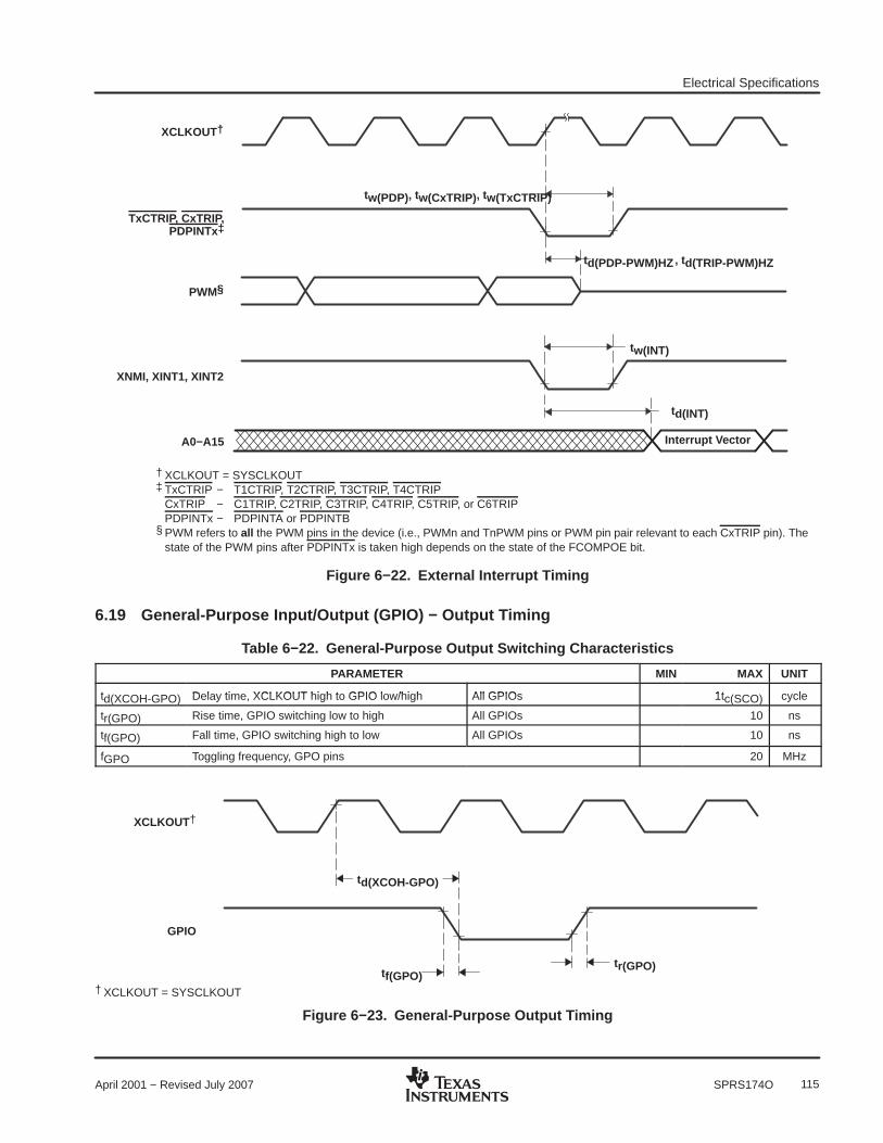
Electrical Specifications
115April 2001 − Revised July 2007 SPRS174O
PWM§
TxCTRIP, CxTRIP,PDPINTx‡
XCLKOUT†
tw(PDP), tw(CxTRIP) , tw(TxCTRIP)
td(PDP-PWM)HZ , td(TRIP-PWM)HZ
XNMI, XINT1, XINT2
tw(INT)
Interrupt Vector
td(INT)
† XCLKOUT = SYSCLKOUT‡ TxCTRIP − T1CTRIP, T2CTRIP, T3CTRIP, T4CTRIP
CxTRIP − C1TRIP, C2TRIP, C3TRIP, C4TRIP, C5TRIP, or C6TRIPPDPINTx − PDPINTA or PDPINTB
§ PWM refers to all the PWM pins in the device (i.e., PWMn and TnPWM pins or PWM pin pair relevant to each CxTRIP pin). Thestate of the PWM pins after PDPINTx is taken high depends on the state of the FCOMPOE bit.
A0−A15
Figure 6−22. External Interrupt Timing
6.19 General-Purpose Input/Output (GPIO) − Output Timing
Table 6−22. General-Purpose Output Switching Characteristics
PARAMETER MIN MAX UNIT
td(XCOH-GPO) Delay time, XCLKOUT high to GPIO low/high All GPIOs 1tc(SCO) cycletd(XCOH-GPO) Delay time, XCLKOUT high to GPIO low/high All GPIOs 1tc(SCO) cycle
tr(GPO) Rise time, GPIO switching low to high All GPIOs 10 ns
tf(GPO) Fall time, GPIO switching high to low All GPIOs 10 ns
fGPO Toggling frequency, GPO pins 20 MHz
td(XCOH-GPO)
GPIO
XCLKOUT†
tr(GPO)tf(GPO)
† XCLKOUT = SYSCLKOUT
Figure 6−23. General-Purpose Output Timing

Electrical Specifications
116 April 2001 − Revised July 2007SPRS174O
6.20 General-Purpose Input/Output (GPIO) − Input Timing
GPIOSignal
1
Sampling Window
Output FromQualifier
1 1 1 1 1 1 1 1 1 1 10 0 0 0 0 0 0 0 0 0
SYSCLKOUT
QUALPRD = 1(SYSCLKOUT/2)
NOTES: A. This glitch is ignored by the input qualifier. The QUALPRD bit field specifies the qualification sampling period. It can vary from00 to 0xFF. Input qualification is not applicable when QUALPRD = 00. For any other value “n”, the qualification sampling periodin 2n SYSCLKOUT cycles (i.e., at every 2n SYSCLKOUT cycle, the GPIO pin will be sampled). Six consecutive samples mustbe of the same value for a given input to be recognized.
B. For the qualifier to detect the change, the input must be stable for 10 SYSCLKOUT cycles or greater. In other words, the inputsshould be stable for (5 × QUALPRD × 2) SYSCLKOUT cycles. This would enable five sampling periods for detection to occur.Since external signals are driven asynchronously, a 13-SYSCLKOUT-wide pulse provides reliable recognition.
See Note A
Sampling period, determined by GPxQUAL[QUALPRD]
(SYSCLKOUT cycle 2 QUALPRD) 5
Figure 6−24. GPIO Input Qualifier − Example Diagram for QUALPRD = 1
Table 6−23. General-Purpose Input Timing Requirements
MIN MAX UNIT
tw(GPI) Pulse duration, GPIO low/high All GPIOsWith no qualifier 2tc(SCO)
cyclestw(GPI) Pulse duration, GPIO low/high All GPIOsWith qualifier 1tc(SCO) + IQT† cycles
† Input Qualification Time (IQT) = [tc(SCO) × 2 × QUALPRD] × 5 + [tc(SCO) × 2 × QUALPRD].
GPIOxn
XCLKOUT
tw(GPI)
Figure 6−25. General-Purpose Input Timing
NOTE: The pulse width requirement for general-purpose input is applicable for the XBIO and ADCSOCpins as well.

Electrical Specifications
117April 2001 − Revised July 2007 SPRS174O
6.21
SP
I Mas
ter
Mod
e T
imin
g
Tabl
e 6−
24.
SP
I Mas
ter
Mod
e E
xter
nal T
imin
g (C
lock
Pha
se =
0)
†‡
NO
.
SP
I WH
EN
(S
PIB
RR
+ 1
) IS
EV
EN
OR
SP
IBR
R =
0 O
R 2
SP
I WH
EN
(S
PIB
RR
+ 1
)IS
OD
D A
ND
SP
IBR
R >
3U
NIT
NO
.M
INM
AX
MIN
MA
XU
NIT
1t c
(SP
C)M
Cyc
le ti
me,
SP
ICLK
4tc(
LCO
)12
8tc(
LCO
)5t
c(LC
O)
127t
c(LC
O)
ns
2§t w
(SP
CH
)MP
ulse
dur
atio
n, S
PIC
LK h
igh
(clo
ck p
olar
ity =
0)
0.5t
c(S
PC
)M−
100.
5tc(
SP
C)M
0.5t
c(S
PC
)M−
0.5t
c(LC
O)−
100.
5tc(
SP
C)M
−0.
5tc(
LCO
)ns
2§
t w(S
PC
L)M
Pul
se d
urat
ion,
SP
ICLK
low
(clo
ck p
olar
ity =
1)
0.5t
c(S
PC
)M−
100.
5tc(
SP
C)M
0.5t
c(S
PC
)M−
0.5t
c(LC
O)−
100.
5tc(
SP
C)M
−0.
5tc(
LCO
)
ns
3§t w
(SP
CL)
MP
ulse
dur
atio
n, S
PIC
LK lo
w(c
lock
pol
arity
= 0
)0.
5tc(
SP
C)M
−10
0.5t
c(S
PC
)M0.
5tc(
SP
C)M
+0.
5tc(
LCO
)−10
0.5t
c(S
PC
)M +
0.5
t c(L
CO
)ns
3§
t w(S
PC
H)M
Pul
se d
urat
ion,
SP
ICLK
hig
h(c
lock
pol
arity
= 1
)0.
5tc(
SP
C)M
−10
0.5t
c(S
PC
)M0.
5tc(
SP
C)M
+0.
5tc(
LCO
)−10
0.5t
c(S
PC
)M +
0.5
t c(L
CO
)
ns
4§t d
(SP
CH
-SIM
O)M
Del
ay ti
me,
SP
ICLK
hig
h to
SP
ISIM
O v
alid
(cl
ock
pola
rity
= 0
)−
1010
− 10
10
ns4§
t d(S
PC
L-S
IMO
)MD
elay
tim
e, S
PIC
LK lo
w to
SP
ISIM
O v
alid
(cl
ock
pola
rity
= 1
)−
1010
− 10
10ns
5§
t v(S
PC
L-S
IMO
)M
Val
id ti
me,
SP
ISIM
O d
ata
valid
afte
r S
PIC
LK lo
w(c
lock
pol
arity
= 0
)0.
5tc(
SP
C)M
−10
0.5t
c(S
PC
)M+
0.5t
c(LC
O)−
10
ns5§
t v(S
PC
H-S
IMO
)M
Val
id ti
me,
SP
ISIM
O d
ata
valid
afte
r S
PIC
LK h
igh
(clo
ck p
olar
ity =
1)
0.5t
c(S
PC
)M−
100.
5tc(
SP
C)M
+0.
5tc(
LCO
)−10
ns
8§t s
u(S
OM
I-S
PC
L)M
Set
up ti
me,
SP
ISO
MI b
efor
e S
PIC
LK lo
w (
cloc
k po
larit
y =
0)
00
ns8§
t su(
SO
MI-
SP
CH
)MS
etup
tim
e, S
PIS
OM
I bef
ore
SP
ICLK
hig
h (c
lock
pol
arity
= 1
)0
0ns
9§
t v(S
PC
L-S
OM
I)M
Val
id ti
me,
SP
ISO
MI d
ata
valid
afte
r S
PIC
LK lo
w(c
lock
pol
arity
= 0
)0.
25t c
(SP
C)M
−10
0.5t
c(S
PC
)M−
0.5t
c(LC
O)−
10
ns9§
t v(S
PC
H-S
OM
I)M
Val
id ti
me,
SP
ISO
MI d
ata
valid
afte
r S
PIC
LK h
igh
(clo
ck p
olar
ity =
1)
0.25
t c(S
PC
)M−
100.
5tc(
SP
C)M
−0.
5tc(
LCO
)−10
ns
†T
he M
AS
TE
R/S
LAV
E b
it (S
PIC
TL.
2) is
set
and
the
CLO
CK
PH
AS
E b
it (S
PIC
TL.
3) is
cle
ared
.
‡t c
(SP
C)
= S
PI c
lock
cyc
le ti
me
= LS
PC
LK4
or
LSP
CLK
(SP
IBR
R
1)t c
(LC
O)
= L
SP
CLK
cyc
le ti
me
§T
he a
ctiv
e ed
ge o
f the
SP
ICLK
sig
nal r
efer
ence
d is
con
trol
led
by th
e C
LOC
K P
OLA
RIT
Y b
it (S
PIC
CR
.6).
NO
TE
:In
tern
al c
lock
pre
scal
ers
mus
t be
adju
sted
suc
h th
at th
e S
PI c
lock
spe
ed is
lim
ited
to th
e fo
llow
ing
SP
I clo
ck r
ate:
Mas
ter
mod
e tr
ansm
it: 2
0 M
Hz
MA
X, m
aste
r m
ode
rece
ive
12.5
MH
z M
AX
Sla
ve m
ode
tran
smit
12.5
MH
z M
AX
, sla
ve m
ode
rece
ive
12.5
MH
z M
AX
.

Electrical Specifications
118 April 2001 − Revised July 2007SPRS174O
9
4
SPISOMI
SPISIMO
SPICLK (clock polarity = 1)
SPICLK (clock polarity = 0)
Master In DataMust Be Valid
Master Out Data Is Valid
8
5
3
2
1
SPISTE†
† In the master mode, SPISTE goes active 0.5tc(SPC) before valid SPI clock edge. On the trailing end of the word, theSPISTE will go inactive 0.5tc(SPC) after the receiving edge (SPICLK) of the last data bit, except that SPISTE stays activebetween back-to-back transmit words in both FIFO and nonFIFO modes.
Figure 6−26. SPI Master Mode External Timing (Clock Phase = 0)

Electrical Specifications
119April 2001 − Revised July 2007 SPRS174O
Tabl
e 6−
25.
SP
I Mas
ter
Mod
e E
xter
nal T
imin
g (C
lock
Pha
se =
1)
†‡
NO
.
SP
I WH
EN
(S
PIB
RR
+ 1
) IS
EV
EN
OR
SP
IBR
R =
0 O
R 2
SP
I WH
EN
(S
PIB
RR
+ 1
)IS
OD
D A
ND
SP
IBR
R >
3U
NIT
NO
.M
INM
AX
MIN
MA
XU
NIT
1t c
(SP
C)M
Cyc
le ti
me,
SP
ICLK
4tc(
LCO
)12
8tc(
LCO
)5t
c(LC
O)
127t
c(LC
O)
ns
2§t w
(SP
CH
)MP
ulse
dur
atio
n, S
PIC
LK h
igh
(clo
ck p
olar
ity =
0)
0.5t
c(S
PC
)M−
100.
5tc(
SP
C)M
0.5t
c(S
PC
)M−
0.5t
c(L
CO
)−10
0.5t
c(S
PC
)M −
0.5t
c(LC
O)
ns2§
t w(S
PC
L)M
Pul
se d
urat
ion,
SP
ICLK
low
(cl
ock
pola
rity
= 1
)0.
5tc(
SP
C)M
−10
0.5t
c(S
PC
)M0.
5tc(
SP
C)M
−0.
5tc
(LC
O)−
100.
5tc(
SP
C)M
−0.
5tc(
LCO
)
ns
3§t w
(SP
CL)
MP
ulse
dur
atio
n, S
PIC
LK lo
w (
cloc
kpo
larit
y =
0)
0.5t
c(S
PC
)M−
100.
5tc(
SP
C)M
0.5t
c(S
PC
)M+
0.5t
c(LC
O)−
100.
5tc(
SP
C)M
+ 0
.5t c
(LC
O)
ns3§
t w(S
PC
H)M
Pul
se d
urat
ion,
SP
ICLK
hig
h(c
lock
pol
arity
= 1
)0.
5tc(
SP
C)M
−10
0.5t
c(S
PC
)M0.
5tc(
SP
C)M
+0.
5tc(
LCO
)−10
0.5t
c(S
PC
)M +
0.5
t c(L
CO
)
ns
6§t s
u(S
IMO
-SP
CH
)M
Set
up ti
me,
SP
ISIM
O d
ata
valid
befo
re S
PIC
LK h
igh
(clo
ck p
olar
ity =
0)
0.5t
c(S
PC
)M−
100.
5tc(
SP
C)M
−10
ns6§
t su(
SIM
O-S
PC
L)M
Set
up ti
me,
SP
ISIM
O d
ata
valid
befo
re S
PIC
LK lo
w (
cloc
k po
larit
y =
1)
0.5t
c(S
PC
)M−
100.
5tc(
SP
C)M
−10
ns
7§t v
(SP
CH
-SIM
O)M
Val
id ti
me,
SP
ISIM
O d
ata
valid
afte
rS
PIC
LK h
igh
(clo
ck p
olar
ity =
0)
0.5t
c(S
PC
)M−
100.
5tc(
SP
C)M
−10
ns7§
t v(S
PC
L-S
IMO
)MV
alid
tim
e, S
PIS
IMO
dat
a va
lid a
fter
SP
ICLK
low
(cl
ock
pola
rity
= 1
)0.
5tc(
SP
C)M
−10
0.5t
c(S
PC
)M −
10ns
10§
t su(
SO
MI-S
PC
H)M
Set
up ti
me,
SP
ISO
MI b
efor
e S
PIC
LKhi
gh (
cloc
k po
larit
y =
0)
00
ns10
§
t su(
SO
MI-
SP
CL)
MS
etup
tim
e, S
PIS
OM
I bef
ore
SP
ICLK
low
(cl
ock
pola
rity
= 1
)0
0ns
11§
t v(S
PC
H-S
OM
I)M
Val
id ti
me,
SP
ISO
MI d
ata
valid
afte
rS
PIC
LK h
igh
(clo
ck p
olar
ity =
0)
0.25
t c(S
PC
)M−
100.
5tc(
SP
C)M
−10
ns11
§
t v(S
PC
L-S
OM
I)M
Val
id ti
me,
SP
ISO
MI d
ata
valid
afte
rS
PIC
LK lo
w (
cloc
k po
larit
y =
1)
0.25
t c(S
PC
)M−
100.
5tc(
SP
C)M
−10
ns
†T
he M
AS
TE
R/S
LAV
E b
it (S
PIC
TL.
2) is
set
and
the
CLO
CK
PH
AS
E b
it (S
PIC
TL.
3) is
set
.
‡t c
(SP
C)
= S
PI c
lock
cyc
le ti
me
= LS
PC
LK4
or
LSP
CLK
(SP
IBR
R
1)
t c(L
CO
) =
LS
PC
LK c
ycle
tim
e§
The
act
ive
edge
of t
he S
PIC
LK s
igna
l ref
eren
ced
is c
ontr
olle
d by
the
CLO
CK
PO
LAR
ITY
bit
(SP
ICC
R.6
).
NO
TE
:In
tern
al c
lock
pre
scal
ers
mus
t be
adju
sted
suc
h th
at th
e S
PI c
lock
spe
ed is
lim
ited
to th
e fo
llow
ing
SP
I clo
ck r
ate:
Mas
ter
mod
e tr
ansm
it: 2
0 M
Hz
MA
X, m
aste
r m
ode
rece
ive
12.5
MH
z M
AX
Sla
ve m
ode
tran
smit
12.5
MH
z M
AX
, sla
ve m
ode
rece
ive
12.5
MH
z M
AX
.


Electrical Specifications
120 April 2001 − Revised July 2007SPRS174O
Data Valid
11
SPISOMI
SPISIMO
SPICLK (clock polarity = 1)
SPICLK (clock polarity = 0)
Master In DataMust Be Valid
Master Out Data Is Valid
1
7
6
10
3
2
SPISTE†
† In the master mode, SPISTE goes active 0.5tc(SPC) before valid SPI clock edge. On the trailing end of the word, theSPISTE will go inactive 0.5tc(SPC) after the receiving edge (SPICLK) of the last data bit, except that SPISTE stays activebetween back-to-back transmit words in both FIFO and nonFIFO modes.
Figure 6−27. SPI Master External Timing (Clock Phase = 1)

Electrical Specifications
121April 2001 − Revised July 2007 SPRS174O
6.22 SPI Slave Mode Timing
Table 6−26. SPI Slave Mode External Timing (Clock Phase = 0) †‡
NO. MIN MAX UNIT
12 tc(SPC)S Cycle time, SPICLK 4tc(LCO)‡ ns
13§tw(SPCH)S Pulse duration, SPICLK high (clock polarity = 0) 0.5tc(SPC)S−10 0.5tc(SPC)S
ns13§tw(SPCL)S Pulse duration, SPICLK low (clock polarity = 1) 0.5tc(SPC)S−10 0.5tc(SPC)S
ns
14§tw(SPCL)S Pulse duration, SPICLK low (clock polarity = 0) 0.5tc(SPC)S−10 0.5tc(SPC)S
ns14§tw(SPCH)S Pulse duration, SPICLK high (clock polarity = 1) 0.5tc(SPC)S−10 0.5tc(SPC)S
ns
15§td(SPCH-SOMI)S
Delay time, SPICLK high to SPISOMI valid(clock polarity = 0)
0.375tc(SPC)S−10ns15§
td(SPCL-SOMI)S Delay time, SPICLK low to SPISOMI valid (clock polarity = 1) 0.375tc(SPC)S−10
ns
16§tv(SPCL-SOMI)S
Valid time, SPISOMI data valid after SPICLK low(clock polarity =0)
0.75tc(SPC)Sns16§
tv(SPCH-SOMI)SValid time, SPISOMI data valid after SPICLK high(clock polarity =1)
0.75tc(SPC)S
ns
19§tsu(SIMO-SPCL)S Setup time, SPISIMO before SPICLK low (clock polarity = 0) 0
ns19§tsu(SIMO-SPCH)S Setup time, SPISIMO before SPICLK high (clock polarity = 1) 0
ns
20§tv(SPCL-SIMO)S
Valid time, SPISIMO data valid after SPICLK low(clock polarity = 0)
0.5tc(SPC)Sns20§
tv(SPCH-SIMO)SValid time, SPISIMO data valid after SPICLK high(clock polarity = 1)
0.5tc(SPC)S
ns
† The MASTER/SLAVE bit (SPICTL.2) is cleared and the CLOCK PHASE bit (SPICTL.3) is cleared.
‡ tc(SPC) = SPI clock cycle time = LSPCLK4
or LSPCLK(SPIBRR 1)
tc(LCO) = LSPCLK cycle time§ The active edge of the SPICLK signal referenced is controlled by the CLOCK POLARITY bit (SPICCR.6).NOTE: Internal clock prescalers must be adjusted such that the SPI clock speed is limited to the following SPI clock rate:
Master mode transmit: 20 MHz MAX, master mode receive 12.5 MHz MAX Slave mode transmit 12.5 MHz MAX, slave mode receive 12.5 MHz MAX.
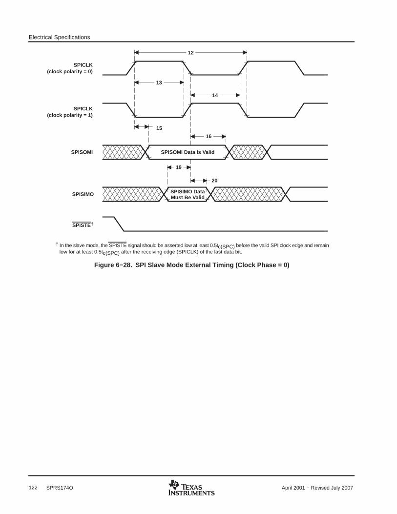
Electrical Specifications
122 April 2001 − Revised July 2007SPRS174O
20
15
SPISIMO
SPISOMI
SPICLK(clock polarity = 1)
SPICLK(clock polarity = 0)
SPISIMO DataMust Be Valid
SPISOMI Data Is Valid
19
16
14
13
12
SPISTE†
† In the slave mode, the SPISTE signal should be asserted low at least 0.5tc(SPC) before the valid SPI clock edge and remainlow for at least 0.5tc(SPC) after the receiving edge (SPICLK) of the last data bit.
Figure 6−28. SPI Slave Mode External Timing (Clock Phase = 0)
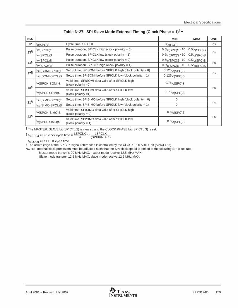
Electrical Specifications
123April 2001 − Revised July 2007 SPRS174O
Table 6−27. SPI Slave Mode External Timing (Clock Phase = 1) †‡
NO. MIN MAX UNIT
12 tc(SPC)S Cycle time, SPICLK 8tc(LCO) ns
13§tw(SPCH)S Pulse duration, SPICLK high (clock polarity = 0) 0.5tc(SPC)S−10 0.5tc(SPC)S
ns13§tw(SPCL)S Pulse duration, SPICLK low (clock polarity = 1) 0.5tc(SPC)S−10 0.5tc(SPC)S
ns
14§tw(SPCL)S Pulse duration, SPICLK low (clock polarity = 0) 0.5tc(SPC)S−10 0.5tc(SPC)S
ns14§tw(SPCH)S Pulse duration, SPICLK high (clock polarity = 1) 0.5tc(SPC)S−10 0.5tc(SPC)S
ns
17§tsu(SOMI-SPCH)S Setup time, SPISOMI before SPICLK high (clock polarity = 0) 0.125tc(SPC)S
ns17§tsu(SOMI-SPCL)S Setup time, SPISOMI before SPICLK low (clock polarity = 1) 0.125tc(SPC)S
ns
18§tv(SPCH-SOMI)S
Valid time, SPISOMI data valid after SPICLK high(clock polarity =0)
0.75tc(SPC)Sns18§
tv(SPCL-SOMI)SValid time, SPISOMI data valid after SPICLK low(clock polarity =1)
0.75tc(SPC)S
ns
21§tsu(SIMO-SPCH)S Setup time, SPISIMO before SPICLK high (clock polarity = 0) 0
ns21§tsu(SIMO-SPCL)S Setup time, SPISIMO before SPICLK low (clock polarity = 1) 0
ns
22§tv(SPCH-SIMO)S
Valid time, SPISIMO data valid after SPICLK high(clock polarity = 0)
0.5tc(SPC)Sns22§
tv(SPCL-SIMO)SValid time, SPISIMO data valid after SPICLK low(clock polarity = 1)
0.5tc(SPC)S
ns
† The MASTER/SLAVE bit (SPICTL.2) is cleared and the CLOCK PHASE bit (SPICTL.3) is set.
‡ tc(SPC) = SPI clock cycle time = LSPCLK4
or LSPCLK(SPIBRR 1)
tc(LCO) = LSPCLK cycle time§ The active edge of the SPICLK signal referenced is controlled by the CLOCK POLARITY bit (SPICCR.6).NOTE: Internal clock prescalers must be adjusted such that the SPI clock speed is limited to the following SPI clock rate:
Master mode transmit: 20 MHz MAX, master mode receive 12.5 MHz MAX Slave mode transmit 12.5 MHz MAX, slave mode receive 12.5 MHz MAX.

Electrical Specifications
124 April 2001 − Revised July 2007SPRS174O
Data Valid
22
SPISIMO
SPISOMI
SPICLK(clock polarity = 1)
SPICLK(clock polarity = 0)
SPISIMO DataMust Be Valid
SPISOMI Data Is Valid
21
12
18
17
14
13
SPISTE†
† In the slave mode, the SPISTE signal should be asserted low at least 0.5tc(SPC) before the valid SPI clock edge andremain low for at least 0.5tc(SPC) after the receiving edge (SPICLK) of the last data bit.
Figure 6−29. SPI Slave Mode External Timing (Clock Phase = 1)

Electrical Specifications
125April 2001 − Revised July 2007 SPRS174O
6.23 External Interface (XINTF) Timing
Each XINTF access consists of three parts: Lead, Active, and Trail. The user configures the Lead/Active/Trailwait states in the XTIMING registers. There is one XTIMING register for each XINTF zone. Table 6−28 showsthe relationship between the parameters configured in the XTIMING register and the duration of the pulse interms of XTIMCLK cycles.
Table 6−28. Relationship Between Parameters Configured in XTIMING and Duration of Pulse †‡
DESCRIPTIONDURATION (ns)
DESCRIPTIONX2TIMING = 0 X2TIMING = 1
LR Lead period, read access XRDLEAD × tc(XTIM) (XRDLEAD × 2) × tc(XTIM)
AR Active period, read access (XRDACTIVE + WS + 1) × tc(XTIM) (XRDACTIVE × 2 + WS + 1) × tc(XTIM)
TR Trail period, read access XRDTRAIL × tc(XTIM) (XRDTRAIL × 2) × tc(XTIM)LW Lead period, write access XWRLEAD × tc(XTIM) (XWRLEAD × 2) × tc(XTIM)
AW Active period, write access (XWRACTIVE + WS + 1) × tc(XTIM) (XWRACTIVE × 2 + WS + 1) × tc(XTIM)TW Trail period, write access XWRTRAIL × tc(XTIM) (XWRTRAIL × 2) × tc(XTIM)
† tc(XTIM) − Cycle time, XTIMCLK‡ WS refers to the number of wait states inserted by hardware when using XREADY. If the zone is configured to ignore XREADY (USEREADY = 0),
then WS = 0.
Minimum wait state requirements must be met when configuring each zone’s XTIMING register. Theserequirements are in addition to any timing requirements as specified by that device’s data sheet. No internaldevice hardware is included to detect illegal settings.
• If the XREADY signal is ignored (USEREADY = 0), then:
1. Lead: LR ≥ tc(XTIM)LW ≥ tc(XTIM)
These requirements result in the following XTIMING register configuration restrictions§:
XRDLEAD XRDACTIVE XRDTRAIL XWRLEAD XWRACTIVE XWRTRAIL X2TIMING
≥ 1 ≥ 0 ≥ 0 ≥ 1 ≥ 0 ≥ 0 0, 1
§ No hardware to detect illegal XTIMING configurations
Examples of valid and invalid timing when not sampling XREADY§:
XRDLEAD XRDACTIVE XRDTRAIL XWRLEAD XWRACTIVE XWRTRAIL X2TIMING
Invalid 0 0 0 0 0 0 0, 1
Valid 1 0 0 1 0 0 0, 1
§ No hardware to detect illegal XTIMING configurations
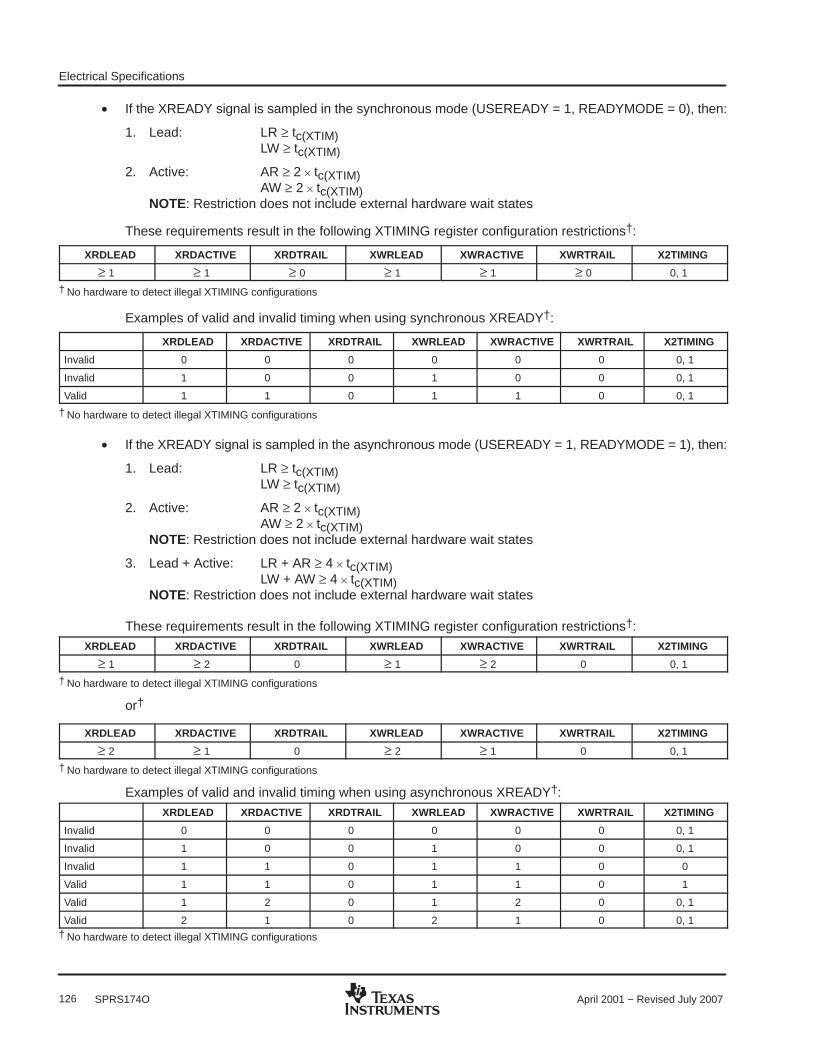
Electrical Specifications
126 April 2001 − Revised July 2007SPRS174O
• If the XREADY signal is sampled in the synchronous mode (USEREADY = 1, READYMODE = 0), then:
1. Lead: LR ≥ tc(XTIM)LW ≥ tc(XTIM)
2. Active: AR ≥ 2 × tc(XTIM)AW ≥ 2 × tc(XTIM)
NOTE: Restriction does not include external hardware wait states
These requirements result in the following XTIMING register configuration restrictions†:
XRDLEAD XRDACTIVE XRDTRAIL XWRLEAD XWRACTIVE XWRTRAIL X2TIMING
≥ 1 ≥ 1 ≥ 0 ≥ 1 ≥ 1 ≥ 0 0, 1
† No hardware to detect illegal XTIMING configurations
Examples of valid and invalid timing when using synchronous XREADY†:
XRDLEAD XRDACTIVE XRDTRAIL XWRLEAD XWRACTIVE XWRTRAIL X2TIMING
Invalid 0 0 0 0 0 0 0, 1
Invalid 1 0 0 1 0 0 0, 1
Valid 1 1 0 1 1 0 0, 1
† No hardware to detect illegal XTIMING configurations
• If the XREADY signal is sampled in the asynchronous mode (USEREADY = 1, READYMODE = 1), then:
1. Lead: LR ≥ tc(XTIM)LW ≥ tc(XTIM)
2. Active: AR ≥ 2 × tc(XTIM)AW ≥ 2 × tc(XTIM)
NOTE: Restriction does not include external hardware wait states
3. Lead + Active: LR + AR ≥ 4 × tc(XTIM)LW + AW ≥ 4 × tc(XTIM)
NOTE: Restriction does not include external hardware wait states
These requirements result in the following XTIMING register configuration restrictions†:XRDLEAD XRDACTIVE XRDTRAIL XWRLEAD XWRACTIVE XWRTRAIL X2TIMING
≥ 1 ≥ 2 0 ≥ 1 ≥ 2 0 0, 1
† No hardware to detect illegal XTIMING configurations
or†
XRDLEAD XRDACTIVE XRDTRAIL XWRLEAD XWRACTIVE XWRTRAIL X2TIMING
≥ 2 ≥ 1 0 ≥ 2 ≥ 1 0 0, 1
† No hardware to detect illegal XTIMING configurations
Examples of valid and invalid timing when using asynchronous XREADY†:
XRDLEAD XRDACTIVE XRDTRAIL XWRLEAD XWRACTIVE XWRTRAIL X2TIMING
Invalid 0 0 0 0 0 0 0, 1
Invalid 1 0 0 1 0 0 0, 1
Invalid 1 1 0 1 1 0 0
Valid 1 1 0 1 1 0 1
Valid 1 2 0 1 2 0 0, 1
Valid 2 1 0 2 1 0 0, 1† No hardware to detect illegal XTIMING configurations

Electrical Specifications
127April 2001 − Revised July 2007 SPRS174O
Unless otherwise specified, all XINTF timing is applicable for the clock configurations shown in Table 6−29.
Table 6−29. XINTF Clock Configurations
MODE SYSCLKOUT XTIMCLK XCLKOUT
1Example: 150 MHz
SYSCLKOUT150 MHz
SYSCLKOUT150 MHz
2Example: 150 MHz
SYSCLKOUT150 MHz
1/2 SYSCLKOUT75 MHz
3Example: 150 MHz
1/2 SYSCLKOUT75 MHz
1/2 SYSCLKOUT75 MHz
4Example: 150 MHz
1/2 SYSCLKOUT75 MHz
1/4 SYSCLKOUT37.5 MHz
The relationship between SYSCLKOUT and XTIMCLK is shown in Figure 6−30.
XTIMING0
XTIMING1
XTIMING2
XTIMING6
XTIMING7
XBANK
LEAD/ACTIVE/TRAIL
1†
0
XCLKOUT
/2XTIMCLK1†
0
/2C28xCPU
XINTCNF2(CLKMODE)
XINTCNF2(XTIMCLK)
† Default Value after reset
SYSCLKOUT
XINTCNF2(CLKOFF)
1
0
0
Figure 6−30. Relationship Between XTIMCLK and SYSCLKOUT
6.24 XINTF Signal Alignment to XCLKOUT
For each XINTF access, the number of lead, active, and trail cycles is based on the internal clock XTIMCLK.Strobes such as XRD, XWE, and zone chip-select (XZCS) change state in relationship to the rising edge ofXTIMCLK. The external clock, XCLKOUT, can be configured to be either equal to or one-half the frequencyof XTIMCLK.
For the case where XCLKOUT = XTIMCLK, all of the XINTF strobes will change state with respect to the risingedge of XCLKOUT. For the case where XCLKOUT = one-half XTIMCLK, some strobes will change state eitheron the rising edge of XCLKOUT or the falling edge of XCLKOUT. In the XINTF timing tables, the notationXCOHL is used to indicate that the parameter is with respect to either case; XCLKOUT rising edge (high) orXCLKOUT falling edge (low). If the parameter is always with respect to the rising edge of XCLKOUT, thenotation XCOH is used.
Electrical Specifications
128 April 2001 − Revised July 2007SPRS174O
For the case where XCLKOUT = one-half XTIMCLK, the XCLKOUT edge with which the change will be alignedcan be determined based on the number of XTIMCLK cycles from the start of the access to the point at whichthe signal changes. If this number of XTIMCLK cycles is even, the alignment will be with respect to the risingedge of XCLKOUT. If this number is odd, then the signal will change with respect to the falling edge ofXCLKOUT. Examples include the following:
• Strobes that change at the beginning of an access always align to the rising edge of XCLKOUT. This isbecause all XINTF accesses begin with respect to the rising edge of XCLKOUT.
Examples: XZCSL Zone chip-select active low
XRNWL XR/W active low
• Strobes that change at the beginning of the active period will align to the rising edge of XCLKOUT if thetotal number of lead XTIMCLK cycles for the access is even. If the number of lead XTIMCLK cycles is odd,then the alignment will be with respect to the falling edge of XCLKOUT.
Examples: XRDL XRD active low
XWEL XWE active low
• Strobes that change at the beginning of the trail period will align to the rising edge of XCLKOUT if the totalnumber of lead + active XTIMCLK cycles (including hardware waitstates) for the access is even. If thenumber of lead + active XTIMCLK cycles (including hardware waitstates) is odd, then the alignment willbe with respect to the falling edge of XCLKOUT.
Examples: XRDH XRD inactive high
XWEH XWE inactive high
• Strobes that change at the end of the access will align to the rising edge of XCLKOUT if the total numberof lead + active + trail XTIMCLK cycles (including hardware waitstates) is even. If the number of lead +active + trail XTIMCLK cycles (including hardware waitstates) is odd, then the alignment will be withrespect to the falling edge of XCLKOUT.
Examples: XZCSH Zone chip-select inactive high
XRNWH XR/W inactive high
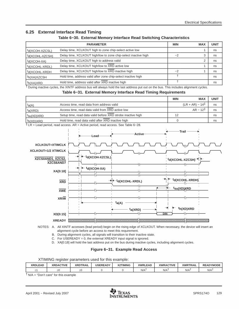
Electrical Specifications
129April 2001 − Revised July 2007 SPRS174O
6.25 External Interface Read TimingTable 6−30. External Memory Interface Read Switching Characteristics
PARAMETER MIN MAX UNIT
td(XCOH-XZCSL) Delay time, XCLKOUT high to zone chip-select active low 1 ns
td(XCOHL-XZCSH) Delay time, XCLKOUT high/low to zone chip-select inactive high −2 3 ns
td(XCOH-XA) Delay time, XCLKOUT high to address valid 2 ns
td(XCOHL-XRDL) Delay time, XCLKOUT high/low to XRD active low 1 ns
td(XCOHL-XRDH Delay time, XCLKOUT high/low to XRD inactive high −2 1 ns
th(XA)XZCSH Hold time, address valid after zone chip-select inactive high † ns
th(XA)XRD Hold time, address valid after XRD inactive high † ns† During inactive cycles, the XINTF address bus will always hold the last address put out on the bus. This includes alignment cycles.
Table 6−31. External Memory Interface Read Timing Requirements
MIN MAX UNIT
ta(A) Access time, read data from address valid (LR + AR) − 14‡ ns
ta(XRD) Access time, read data valid from XRD active low AR − 12‡ ns
tsu(XD)XRD Setup time, read data valid before XRD strobe inactive high 12 ns
th(XD)XRD Hold time, read data valid after XRD inactive high 0 ns‡ LR = Lead period, read access. AR = Active period, read access. See Table 6−28.
LeadActive
Trail
DIN
td(XCOHL-XRDL)
td(XCOH-XA)
td(XCOH-XZCSL)
td(XCOHL-XRDH)
th(XD)XRD
td(XCOHL-XZCSH)
XCLKOUT=XTIMCLK
XCLKOUT=1/2 XTIMCLK
XZCS0AND1, XZCS2,XZCS6AND7
XA[0:18]
XRD
XWE
XR/W
XD[0:15]
NOTES: A. All XINTF accesses (lead period) begin on the rising edge of XCLKOUT. When necessary, the device will insert analignment cycle before an access to meet this requirement.
B. During alignment cycles, all signals will transition to their inactive state.C. For USEREADY = 0, the external XREADY input signal is ignored.D. XA[0:18] will hold the last address put on the bus during inactive cycles, including alignment cycles.
tsu(XD)XRD
ta(A)
ta(XRD)
XREADY
Figure 6−31. Example Read Access
XTIMING register parameters used for this example:XRDLEAD XRDACTIVE XRDTRAIL USEREADY X2TIMING XWRLEAD XWRACTIVE XWRTRAIL READYMODE
≥1 ≥0 ≥0 0 0 N/A† N/A† N/A† N/A†
† N/A = “Don’t care” for this example
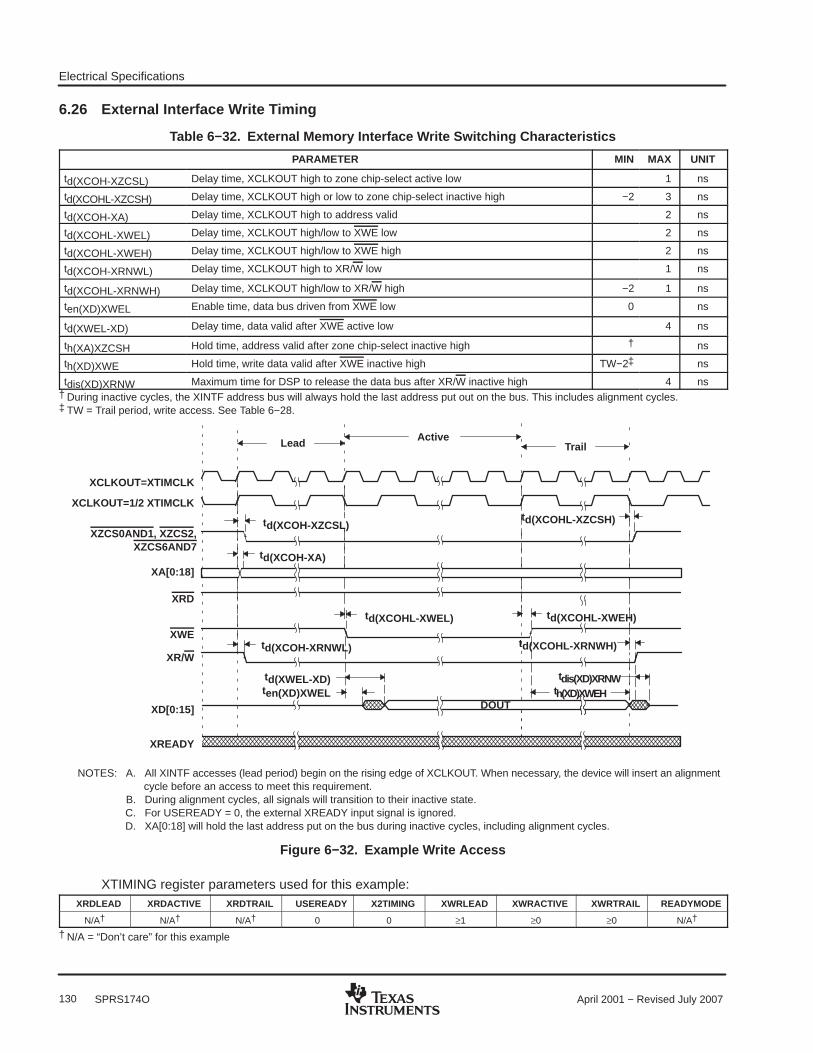
Electrical Specifications
130 April 2001 − Revised July 2007SPRS174O
6.26 External Interface Write Timing
Table 6−32. External Memory Interface Write Switching Characteristics
PARAMETER MIN MAX UNIT
td(XCOH-XZCSL) Delay time, XCLKOUT high to zone chip-select active low 1 ns
td(XCOHL-XZCSH) Delay time, XCLKOUT high or low to zone chip-select inactive high −2 3 ns
td(XCOH-XA) Delay time, XCLKOUT high to address valid 2 ns
td(XCOHL-XWEL) Delay time, XCLKOUT high/low to XWE low 2 ns
td(XCOHL-XWEH) Delay time, XCLKOUT high/low to XWE high 2 ns
td(XCOH-XRNWL) Delay time, XCLKOUT high to XR/W low 1 ns
td(XCOHL-XRNWH) Delay time, XCLKOUT high/low to XR/W high −2 1 ns
ten(XD)XWEL Enable time, data bus driven from XWE low 0 ns
td(XWEL-XD) Delay time, data valid after XWE active low 4 ns
th(XA)XZCSH Hold time, address valid after zone chip-select inactive high † ns
th(XD)XWE Hold time, write data valid after XWE inactive high TW−2‡ ns
tdis(XD)XRNW Maximum time for DSP to release the data bus after XR/W inactive high 4 ns† During inactive cycles, the XINTF address bus will always hold the last address put out on the bus. This includes alignment cycles.‡ TW = Trail period, write access. See Table 6−28.
Lead ActiveTrail
td(XCOH-XZCSL)
td(XCOH-XA)
td(XCOHL-XWEL) td(XCOHL-XWEH)
td(XCOHL-XZCSH)
ten(XD)XWEL th(XD)XWEH
tdis(XD)XRNW
XCLKOUT=XTIMCLK
XCLKOUT=1/2 XTIMCLK
XZCS0AND1, XZCS2,XZCS6AND7
XA[0:18]
XRD
XWE
XR/W
XD[0:15]
NOTES: A. All XINTF accesses (lead period) begin on the rising edge of XCLKOUT. When necessary, the device will insert an alignmentcycle before an access to meet this requirement.
B. During alignment cycles, all signals will transition to their inactive state.C. For USEREADY = 0, the external XREADY input signal is ignored.D. XA[0:18] will hold the last address put on the bus during inactive cycles, including alignment cycles.
td(XCOH-XRNWL) td(XCOHL-XRNWH)
DOUT
XREADY
td(XWEL-XD)
Figure 6−32. Example Write Access
XTIMING register parameters used for this example:XRDLEAD XRDACTIVE XRDTRAIL USEREADY X2TIMING XWRLEAD XWRACTIVE XWRTRAIL READYMODE
N/A† N/A† N/A† 0 0 ≥1 ≥0 ≥0 N/A†
† N/A = “Don’t care” for this example
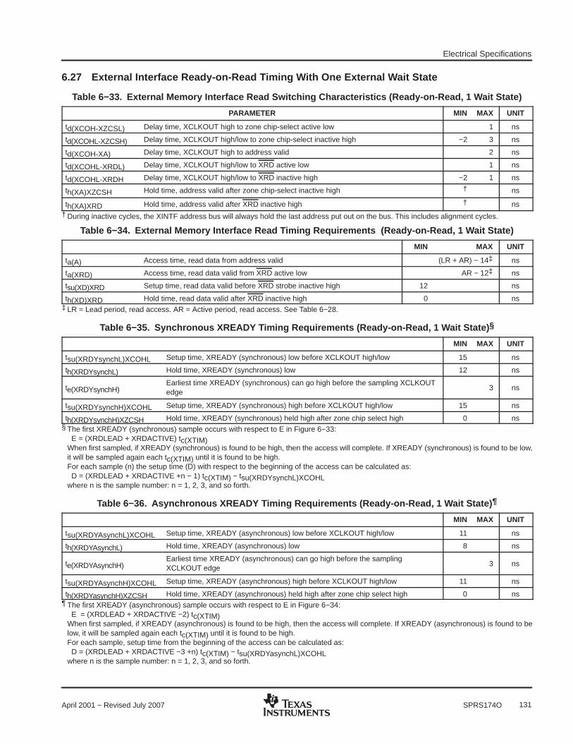
Electrical Specifications
131April 2001 − Revised July 2007 SPRS174O
6.27 External Interface Ready-on-Read Timing With One External Wait State
Table 6−33. External Memory Interface Read Switching Characteristics (Ready-on-Read, 1 Wait State)
PARAMETER MIN MAX UNIT
td(XCOH-XZCSL) Delay time, XCLKOUT high to zone chip-select active low 1 ns
td(XCOHL-XZCSH) Delay time, XCLKOUT high/low to zone chip-select inactive high −2 3 ns
td(XCOH-XA) Delay time, XCLKOUT high to address valid 2 ns
td(XCOHL-XRDL) Delay time, XCLKOUT high/low to XRD active low 1 ns
td(XCOHL-XRDH Delay time, XCLKOUT high/low to XRD inactive high −2 1 ns
th(XA)XZCSH Hold time, address valid after zone chip-select inactive high † ns
th(XA)XRD Hold time, address valid after XRD inactive high † ns† During inactive cycles, the XINTF address bus will always hold the last address put out on the bus. This includes alignment cycles.
Table 6−34. External Memory Interface Read Timing Requirements (Ready-on-Read, 1 Wait State)
MIN MAX UNIT
ta(A) Access time, read data from address valid (LR + AR) − 14‡ ns
ta(XRD) Access time, read data valid from XRD active low AR − 12‡ ns
tsu(XD)XRD Setup time, read data valid before XRD strobe inactive high 12 ns
th(XD)XRD Hold time, read data valid after XRD inactive high 0 ns‡ LR = Lead period, read access. AR = Active period, read access. See Table 6−28.
Table 6−35. Synchronous XREADY Timing Requirements (Ready-on-Read, 1 Wait State) §
MIN MAX UNIT
tsu(XRDYsynchL)XCOHL Setup time, XREADY (synchronous) low before XCLKOUT high/low 15 ns
th(XRDYsynchL) Hold time, XREADY (synchronous) low 12 ns
te(XRDYsynchH)Earliest time XREADY (synchronous) can go high before the sampling XCLKOUTedge
3 ns
tsu(XRDYsynchH)XCOHL Setup time, XREADY (synchronous) high before XCLKOUT high/low 15 ns
th(XRDYsynchH)XZCSH Hold time, XREADY (synchronous) held high after zone chip select high 0 ns§ The first XREADY (synchronous) sample occurs with respect to E in Figure 6−33:
E = (XRDLEAD + XRDACTIVE) tc(XTIM)When first sampled, if XREADY (synchronous) is found to be high, then the access will complete. If XREADY (synchronous) is found to be low,it will be sampled again each tc(XTIM) until it is found to be high.For each sample (n) the setup time (D) with respect to the beginning of the access can be calculated as: D = (XRDLEAD + XRDACTIVE +n − 1) tc(XTIM) − tsu(XRDYsynchL)XCOHLwhere n is the sample number: n = 1, 2, 3, and so forth.
Table 6−36. Asynchronous XREADY Timing Requirements (Ready-on-Read, 1 Wait State) ¶
MIN MAX UNIT
tsu(XRDYAsynchL)XCOHL Setup time, XREADY (asynchronous) low before XCLKOUT high/low 11 ns
th(XRDYAsynchL) Hold time, XREADY (asynchronous) low 8 ns
te(XRDYAsynchH)Earliest time XREADY (asynchronous) can go high before the samplingXCLKOUT edge
3 ns
tsu(XRDYAsynchH)XCOHL Setup time, XREADY (asynchronous) high before XCLKOUT high/low 11 ns
th(XRDYasynchH)XZCSH Hold time, XREADY (asynchronous) held high after zone chip select high 0 ns¶ The first XREADY (asynchronous) sample occurs with respect to E in Figure 6−34:
E = (XRDLEAD + XRDACTIVE −2) tc(XTIM)When first sampled, if XREADY (asynchronous) is found to be high, then the access will complete. If XREADY (asynchronous) is found to below, it will be sampled again each tc(XTIM) until it is found to be high.For each sample, setup time from the beginning of the access can be calculated as: D = (XRDLEAD + XRDACTIVE −3 +n) tc(XTIM) − tsu(XRDYasynchL)XCOHLwhere n is the sample number: n = 1, 2, 3, and so forth.
Electrical Specifications
132 April 2001 − Revised July 2007SPRS174O
LeadActive
Trail
DIN
td(XCOH-XZCSL)
td(XCOH-XA)
td(XCOHL-XRDL)
td(XCOHL-XZCSH)
td(XCOHL-XRDH)
WS (Synch)
XCLKOUT=XTIMCLK
XCLKOUT=1/2 XTIMCLK
XZCS0AND1, XZCS2,XZCS6AND7
XA[0:18]
XRD
XWE
XR/W
XD[0:15]
XREADY(Synch)
NOTES: A. All XINTF accesses (lead period) begin on the rising edge of XCLKOUT. When necessary, the device will insert analignment cycle before an access to meet this requirement.
B. During alignment cycles, all signals will transition to their inactive state.C. During inactive cycles, the XINTF address bus will always hold the last address put out on the bus. This includes
alignment cycles.D. For each sample, setup time from the beginning of the access (D) can be calculated as:
D = (XRDLEAD + XRDACTIVE +n − 1) tc(XTIM) − tsu(XRDYsynchL)XCOHLE. Reference for the first sample is with respect to this point
E = (XRDLEAD + XRDACTIVE) tc(XTIM)where n is the sample number: n = 1, 2, 3, and so forth.
th(XRDYsynchL)
tsu(XRDYsynchL)XCOHL
tsu(XD)XRDta(XRD)
ta(A)th(XD)XRD
th(XRDYsynchH)XZCSH
= Don’t care. Signal can be high or low during this time.
Legend:
tsu(XRDHsynchH)XCOHL
See Note D
See Note E
te(XRDYsynchH)
See Note D
See Notes A and B
See Note C
Figure 6−33. Example Read With Synchronous XREADY Access
XTIMING register parameters used for this example:XRDLEAD XRDACTIVE XRDTRAIL USEREADY X2TIMING XWRLEAD XWRACTIVE XWRTRAIL READYMODE
≥1 3 ≥1 1 0 N/A† N/A† N/A† 0 = XREADY(Synch)
† N/A = “Don’t care” for this example

Electrical Specifications
133April 2001 − Revised July 2007 SPRS174O
tsu(XD)XRD
LeadActive
Trail
DIN
td(XCOH-XZCSL)
td(XCOH-XA)
td(XCOHL-XRDL)
td(XCOHL-XZCSH)
td(XCOHL-XRDH)
WS (Async)
XCLKOUT=XTIMCLK
XCLKOUT=1/2 XTIMCLK
XZCS0AND1, XZCS2,XZCS6AND7
XA[0:18]
XRD
XWE
XR/W
XD[0:15]
XREADY(Asynch)
NOTES: A. All XINTF accesses (lead period) begin on the rising edge of XCLKOUT. When necessary, the device will insert an alignmentcycle before an access to meet this requirement.
B. During alignment cycles, all signals will transition to their inactive state.C. During inactive cycles, the XINTF address bus will always hold the last address put out on the bus. This includes alignment
cycles.D. For each sample, setup time from the beginning of the access can be calculated as:
D = (XRDLEAD + XRDACTIVE −3 +n) tc(XTIM) − tsu(XRDYasynchL)XCOHLwhere n is the sample number: n = 1, 2, 3, and so forth.
E. Reference for the first sample is with respect to this point: E = (XRDLEAD + XRDACTIVE −2) tc(XTIM)
tsu(XRDYasynchL)XCOHL
ta(XRD)
ta(A)
th(XRDYasynchL)
th(XD)XRD
th(XRDYasynchH)XZCSH
= Don’t care. Signal can be high or low during this time.Legend:
" #
See Note C
tsu(XRDYasynchH)XCOHL
See Note D
See Note E
te(XRDYasynchH)
Figure 6−34. Example Read With Asynchronous XREADY Access
XTIMING register parameters used for this example:XRDLEAD XRDACTIVE XRDTRAIL USEREADY X2TIMING XWRLEAD XWRACTIVE XWRTRAIL READYMODE
≥1 3 ≥1 1 0 N/A† N/A† N/A† 1 = XREADY (Async)
† N/A = “Don’t care” for this example
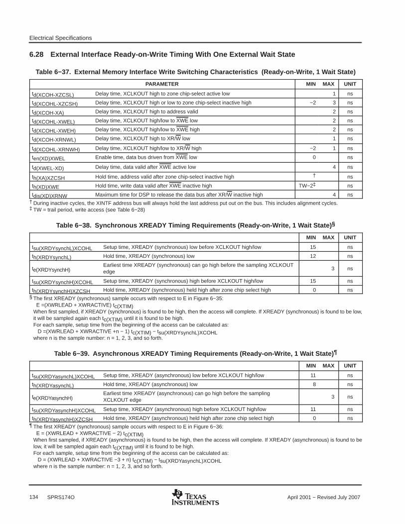
Electrical Specifications
134 April 2001 − Revised July 2007SPRS174O
6.28 External Interface Ready-on-Write Timing With One External Wait State
Table 6−37. External Memory Interface Write Switching Characteristics (Ready-on-Write, 1 Wait State)
PARAMETER MIN MAX UNIT
td(XCOH-XZCSL) Delay time, XCLKOUT high to zone chip-select active low 1 ns
td(XCOHL-XZCSH) Delay time, XCLKOUT high or low to zone chip-select inactive high −2 3 ns
td(XCOH-XA) Delay time, XCLKOUT high to address valid 2 ns
td(XCOHL-XWEL) Delay time, XCLKOUT high/low to XWE low 2 ns
td(XCOHL-XWEH) Delay time, XCLKOUT high/low to XWE high 2 ns
td(XCOH-XRNWL) Delay time, XCLKOUT high to XR/W low 1 ns
td(XCOHL-XRNWH) Delay time, XCLKOUT high/low to XR/W high −2 1 ns
ten(XD)XWEL Enable time, data bus driven from XWE low 0 ns
td(XWEL-XD) Delay time, data valid after XWE active low 4 ns
th(XA)XZCSH Hold time, address valid after zone chip-select inactive high † ns
th(XD)XWE Hold time, write data valid after XWE inactive high TW−2‡ ns
tdis(XD)XRNW Maximum time for DSP to release the data bus after XR/W inactive high 4 ns† During inactive cycles, the XINTF address bus will always hold the last address put out on the bus. This includes alignment cycles.‡ TW = trail period, write access (see Table 6−28)
Table 6−38. Synchronous XREADY Timing Requirements (Ready-on-Write, 1 Wait State) §
MIN MAX UNIT
tsu(XRDYsynchL)XCOHL Setup time, XREADY (synchronous) low before XCLKOUT high/low 15 ns
th(XRDYsynchL) Hold time, XREADY (synchronous) low 12 ns
te(XRDYsynchH)Earliest time XREADY (synchronous) can go high before the sampling XCLKOUTedge
3 ns
tsu(XRDYsynchH)XCOHL Setup time, XREADY (synchronous) high before XCLKOUT high/low 15 ns
th(XRDYsynchH)XZCSH Hold time, XREADY (synchronous) held high after zone chip select high 0 ns§ The first XREADY (synchronous) sample occurs with respect to E in Figure 6−35:
E =(XWRLEAD + XWRACTIVE) tc(XTIM)When first sampled, if XREADY (synchronous) is found to be high, then the access will complete. If XREADY (synchronous) is found to be low,it will be sampled again each tc(XTIM) until it is found to be high.For each sample, setup time from the beginning of the access can be calculated as: D =(XWRLEAD + XWRACTIVE +n − 1) tc(XTIM) − tsu(XRDYsynchL)XCOHLwhere n is the sample number: n = 1, 2, 3, and so forth.
Table 6−39. Asynchronous XREADY Timing Requirements (Ready-on-Write, 1 Wait State) ¶
MIN MAX UNIT
tsu(XRDYasynchL)XCOHL Setup time, XREADY (asynchronous) low before XCLKOUT high/low 11 ns
th(XRDYasynchL) Hold time, XREADY (asynchronous) low 8 ns
te(XRDYasynchH)Earliest time XREADY (asynchronous) can go high before the samplingXCLKOUT edge
3 ns
tsu(XRDYasynchH)XCOHL Setup time, XREADY (asynchronous) high before XCLKOUT high/low 11 ns
th(XRDYasynchH)XZCSH Hold time, XREADY (asynchronous) held high after zone chip select high 0 ns¶ The first XREADY (synchronous) sample occurs with respect to E in Figure 6−36:
E = (XWRLEAD + XWRACTIVE − 2) tc(XTIM)When first sampled, if XREADY (asynchronous) is found to be high, then the access will complete. If XREADY (asynchronous) is found to below, it will be sampled again each tc(XTIM) until it is found to be high.For each sample, setup time from the beginning of the access can be calculated as: D = (XWRLEAD + XWRACTIVE −3 + n) tc(XTIM) − tsu(XRDYasynchL)XCOHLwhere n is the sample number: n = 1, 2, 3, and so forth.
Electrical Specifications
135April 2001 − Revised July 2007 SPRS174O
Lead 1Active
Trail
XCLKOUT = XTIMCLK
XCLKOUT = 1/2 XTIMCLK
XA[0:18]
XD[0:15]
XREADY(Synch)
td(XCOHL-XWEL) td(XCOHL-XWEH)
td(XCOHL-XZCSH)
td(XCOH-XA)
WS (Synch)
XZCS0AND1, XZCS2,XZCS6AND7
XRD
XWE
XR/W
td(XCOH-XZCSL)
NOTES: A. All XINTF accesses (lead period) begin on the rising edge of XCLKOUT. When necessary, the device will insert an alignment cycle before anaccess to meet this requirement.
B. During alignment cycles, all signals will transition to their inactive state.C. During inactive cycles, the XINTF address bus will always hold the last address put out on the bus. This includes alignment cycles.D. For each sample, setup time from the beginning of the access can be calculated as
D = (XWRLEAD + XWRACTIVE + n − 1) tc(XTIM) − tsu(XRDYsynchL)XCOHLwhere n is the sample number: n = 1, 2, 3 and so forth.
E. Reference for the first sample is with respect to this point E = (XWRLEAD + XWRACTIVE) tc(XTIM)
td(XCOH-XRNWL) td(XCOHL-XRNWH)
ten(XD)XWELth(XD)XWEH
tsu(XRDHsynchH)XCOHL
tsu(XRDYsynchL)XCOHL
DOUT
td(XWEL-XD) tdis(XD)XRNW
th(XRDYsynchL)
th(XRDYsynchH)XZCSH
= Don’t care. Signal can be high or low during this time.
Legend:
See Note E
See Note D
SeeNotes Aand B
See Note C
te(XRDYsynchH)
Figure 6−35. Write With Synchronous XREADY Access
XTIMING register parameters used for this example:XRDLEAD XRDACTIVE XRDTRAIL USEREADY X2TIMING XWRLEAD XWRACTIVE XWRTRAIL READYMODE
N/A† N/A† N/A† 1 0 ≥1 3 ≥10 = XREADY
(Synch)
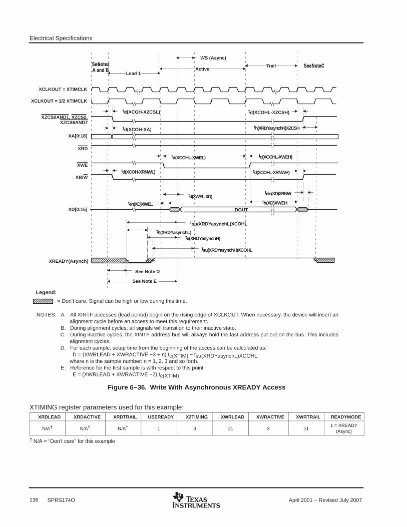
Electrical Specifications
136 April 2001 − Revised July 2007SPRS174O
Lead 1Active
Trail
XCLKOUT = XTIMCLK
XCLKOUT = 1/2 XTIMCLK
XA[0:18]
XD[0:15]
td(XCOHL-XWEH)
td(XCOHL-XZCSH)
td(XCOH-XA)
WS (Async)
XZCS0AND1, XZCS2,XZCS6AND7
XRD
XWE
XR/W
td(XCOH-XZCSL)
NOTES: A. All XINTF accesses (lead period) begin on the rising edge of XCLKOUT. When necessary, the device will insert analignment cycle before an access to meet this requirement.
B. During alignment cycles, all signals will transition to their inactive state.C. During inactive cycles, the XINTF address bus will always hold the last address put out on the bus. This includes
alignment cycles.D. For each sample, setup time from the beginning of the access can be calculated as:
D = (XWRLEAD + XWRACTIVE −3 + n) tc(XTIM) − tsu(XRDYasynchL)XCOHLwhere n is the sample number: n = 1, 2, 3 and so forth.
E. Reference for the first sample is with respect to this point E = (XWRLEAD + XWRACTIVE −2) tc(XTIM)
td(XCOH-XRNWL) td(XCOHL-XRNWH)
ten(XD)XWEL th(XD)XWEH
th(XRDYasynchL)
DOUT
tdis(XD)XRNW
th(XRDYasynchH)XZCSH
See Note E
See Note D
= Don’t care. Signal can be high or low during this time.
Legend:
tsu(XRDYasynchL)XCOHL
tsu(XRDYasynchH)XCOHL
td(XWEL-XD)
td(XCOHL-XWEL)
" #
"
te(XRDYasynchH)
XREADY(Asynch)
Figure 6−36. Write With Asynchronous XREADY Access
XTIMING register parameters used for this example:XRDLEAD XRDACTIVE XRDTRAIL USEREADY X2TIMING XWRLEAD XWRACTIVE XWRTRAIL READYMODE
N/A† N/A† N/A† 1 0 ≥1 3 ≥11 = XREADY
(Async)
† N/A = “Don’t care” for this example
Electrical Specifications
137April 2001 − Revised July 2007 SPRS174O
6.29 XHOLD and XHOLDA
If the HOLD mode bit is set while XHOLD and XHOLDA are both low (external bus accesses granted), theXHOLDA signal is forced high (at the end of the current cycle) and the external interface is taken out ofhigh-impedance mode.
On a reset (XRS), the HOLD mode bit is set to 0. If the XHOLD signal is active low on a system reset, the busand all signal strobes must be in high-impedance mode, and the XHOLDA signal is also driven active low.
When HOLD mode is enabled and XHOLDA is active low (external bus grant active), the CPU can still executecode from internal memory. If an access is made to the external interface, the CPU is stalled until the XHOLDsignal is removed.
An external DMA request, when granted, places the following signals in a high-impedance mode:
XA[18:0] XZCS0AND1
XD[15:0] XZCS2
XWE, XRD XZCS6AND7
XR/W
All other signals not listed in this group remain in their default or functional operational modes during thesesignal events.

Electrical Specifications
138 April 2001 − Revised July 2007SPRS174O
6.30 XHOLD/XHOLDA Timing
Table 6−40. XHOLD /XHOLDA Timing Requirements (XCLKOUT = XTIMCLK) †‡
MIN MAX UNIT
td(HL-HiZ) Delay time, XHOLD low to Hi-Z on all Address, Data, and Control 4tc(XTIM) ns
td(HL-HAL) Delay time, XHOLD low to XHOLDA low 5tc(XTIM) ns
td(HH-HAH) Delay time, XHOLD high to XHOLDA high 3tc(XTIM) ns
td(HH-BV) Delay time, XHOLD high to Bus valid 4tc(XTIM) ns† When a low signal is detected on XHOLD, all pending XINTF accesses will be completed before the bus is placed in a high-impedance state.‡ The state of XHOLD is latched on the rising edge of XTIMCLK.
XCLKOUT(/1 Mode)
XHOLD
XR/W,XZCS0AND1,
XZCS2,XZCS6AND7
XD[15:0] Valid
XHOLDA
td(HL-Hiz)
td(HH-HAH)
High-Impedance
XA[18:0] Valid ValidHigh-Impedance
td(HH-BV)td(HL-HAL)
See Note A See Note B
NOTES: A. All pending XINTF accesses are completed.B. Normal XINTF operation resumes.
Figure 6−37. External Interface Hold Waveform

Electrical Specifications
139April 2001 − Revised July 2007 SPRS174O
Table 6−41. XHOLD /XHOLDA Timing Requirements (XCLKOUT = 1/2 XTIMCLK)†‡§
MIN MAX UNIT
td(HL-HiZ) Delay time, XHOLD low to Hi-Z on all Address, Data, and Control 4tc(XTIM)+tc(XCO) ns
td(HL-HAL) Delay time, XHOLD low to XHOLDA low 4tc(XTIM+2tc(XCO) ns
td(HH-HAH) Delay time, XHOLD high to XHOLDA high 4tc(XTIM) ns
td(HH-BV) Delay time, XHOLD high to Bus valid 6tc(XTIM) ns† When a low signal is detected on XHOLD, all pending XINTF accesses will be completed before the bus is placed in a high-impedance state.‡ The state of XHOLD is latched on the rising edge of XTIMCLK.§ After the XHOLD is detected low or high, all bus transitions and XHOLDA transitions will occur with respect to the rising edge of XCLKOUT. Thus,
for this mode where XCLKOUT = 1/2 XTIMCLK, the transitions can occur up to 1 XTIMCLK cycle earlier than the maximum value specified.
XCLKOUT(1/2 XTIMCLK)
XHOLD
XR/W,XZCS0AND1,
XZCS2,XZCS6AND7
XD[15:0] Valid
XHOLDAtd(HL-HiZ)
td(HH-HAH)
High-Impedance
XA[18:0] Valid ValidHigh-Impedance
td(HH-BV)
td(HL-HAL)
High-Impedance
See Note A See Note B
NOTES: A All pending XINTF accesses are completed.B Normal XINTF operation resumes.
Figure 6−38. XHOLD /XHOLDA Timing Requirements (XCLKOUT = 1/2 XTIMCLK)
Electrical Specifications
140 April 2001 − Revised July 2007SPRS174O
6.31 On-Chip Analog-to-Digital Converter
6.31.1 ADC Absolute Maximum Ratings †
Supply voltage range, VSSA1/VSSA2 to VDDA1/VDDA2/AVDDREFBG −0.3 V to 4.6 V. . . . . . . . . . . . . . .
VSS1 to VDD1 −0.3 V to 2.5 V. . . . . . . . . . . . . . . . . . . . . . . . . . . . . . . . . . . . . . . . . . .
Analog Input (ADCIN) Clamp Current, total (max) ± 20 mA‡. . . . . . . . . . . . . . . . . . . . . . . . . . . . . . . . . . . . . . . . .
† Unless otherwise noted, the list of absolute maximum ratings are specified over operating conditions. Stresses beyond those listed underAbsolute Maximum Ratings may cause permanent damage to the device. These are stress ratings only. Exposure to absolute-maximum-ratedconditions for extended periods may affect device reliability.
‡ The analog inputs have an internal clamping circuit that clamps the voltage to a diode drop above VDDA or below VSS. The continuous clampcurrent per pin is ± 2 mA.
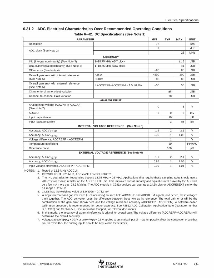
Electrical Specifications
141April 2001 − Revised July 2007 SPRS174O
6.31.2 ADC Electrical Characteristics Over Recommended Operating ConditionsTable 6−42. DC Specifications (See Note 1)
PARAMETER MIN TYP MAX UNIT
Resolution 12 Bits
ADC clock (See Note 2)1 kHz
ADC clock (See Note 2)25 MHz
ACCURACY
INL (Integral nonlinearity) (See Note 3) 1−18.75 MHz ADC clock ±1.5 LSB
DNL (Differential nonlinearity) (See Note 3) 1−18.75 MHz ADC clock ±1 LSB
Offset error (See Note 4) −80 80 LSB
Overall gain error with internal reference F281x −200 200 LSBOverall gain error with internal reference (See Note 5) C281x −80 80 LSB
Overall gain error with external reference (See Note 6)
If ADCREFP−ADCREFM = 1 V ±0.1% −50 50 LSB
Channel-to-channel offset variation ±8 LSB
Channel-to-channel Gain variation ±8 LSB
ANALOG INPUT
Analog input voltage (ADCINx to ADCLO) (See Note 7)
0 3 V
ADCLO −5 0 5 mV
Input capacitance 10 pF
Input leakage current 3 ±5 µA
INTERNAL VOLTAGE REFERENCE (See Note 5)
Accuracy, ADCVREFP 1.9 2 2.1 V
Accuracy, ADCVREFM 0.95 1 1.05 V
Voltage difference, ADCREFP − ADCREFM 1 V
Temperature coefficient 50 PPM/°CReference noise 100 µV
EXTERNAL VOLTAGE REFERENCE (See Note 6)
Accuracy, ADCVREFP 1.9 2 2.1 V
Accuracy, ADCVREFM 0.95 1 1.05 V
Input voltage difference, ADCREFP − ADCREFM 0.99 1 1.01 V
NOTES: 1. Tested at 12.5-MHz ADCCLK2. If SYSCLKOUT ≤ 25 MHz, ADC clock ≤ SYSCLKOUT/23. The INL degrades for frequencies beyond 18.75 MHz − 25 MHz. Applications that require these sampling rates should use a
20K-resistor as bias resistor on the ADCRESEXT pin. This improves overall linearity and typical current drawn by the ADC willbe a few mA more than 24.9 kΩ bias. The ADC module in C281x devices can operate at 24.9k bias on ADCRESEXT pin for thefull range 1−25MHz
4. 1 LSB has the weighted value of 3.0/4096 = 0.732 mV.5. A single internal band gap reference (±5% accuracy) sources both ADCREFP and ADCREFM signals, and hence, these voltages
track together. The ADC converter uses the difference between these two as its reference. The total gain error will be thecombination of the gain error shown here and the voltage reference accuracy (ADCREFP − ADCREFM). A software-basedcalibration procedure is recommended for better accuracy. See F2812 ADC Calibration Application Note (literature numberSPRA989) and Section 5.2, Documentation Support, for relevant documents.
6. In this mode, the accuracy of external reference is critical for overall gain. The voltage difference (ADCREFP−ADCREFM) willdetermine the overall accuracy.
7. Voltages above VDDA + 0.3 V or below VSS − 0.3 V applied to an analog input pin may temporarily affect the conversion of anotherpin. To avoid this, the analog inputs should be kept within these limits.

Electrical Specifications
142 April 2001 − Revised July 2007SPRS174O
Table 6−43. AC SpecificationsPARAMETER MIN TYP MAX UNIT
SINAD Signal-to-noise ratio + distortion 62 dB
SNR Signal-to-noise ratio 62 dB
THD (100 kHz) Total harmonic distortion −68 dB
ENOB (SNR) Effective number of bits 10.1 Bits
SFDR Spurious free dynamic range 69 dB
6.31.3 Current Consumption for Different ADC Configurations (at 25-MHz ADCCLK) ‡
IDDA (TYP)§ IDDAIO (TYP) IDD1 (TYP) ADC OPERATING MODE/CONDITIONS
40 mA 1 µA 0.5 mAMode A (Operational Mode):− BG and REF enabled− PWD disabled
7 mA 0 5 µA
Mode B:− ADC clock enabled− BG and REF enabled− PWD enabled
1 µA 0 5 µA
Mode C:− ADC clock enabled− BG and REF disabled− PWD enabled
1 µA 0 0
Mode D:− ADC clock disabled− BG and REF disabled− PWD enabled
‡ Test Conditions: SYSCLKOUT = 150 MHzADC module clock = 25 MHzADC performing a continuous conversion of all 16 channels in Mode A
§ IDDA − includes current into VDDA1/VDDA2 and AVDDREFBG
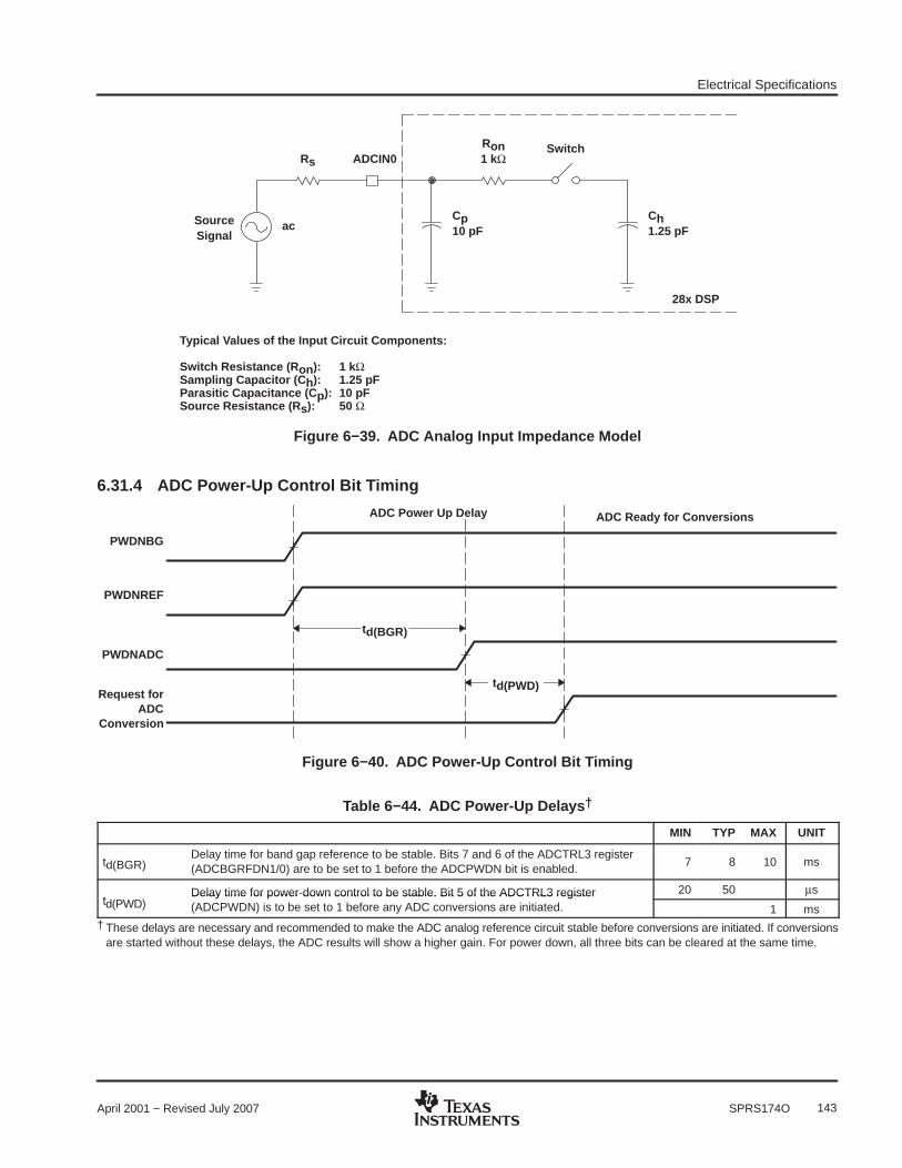
Electrical Specifications
143April 2001 − Revised July 2007 SPRS174O
ac
Rs ADCIN0
Cp10 pF
Ron1 kΩ
1.25 pFCh
Switch
Typical Values of the Input Circuit Components:
Switch Resistance (R on): 1 kΩSampling Capacitor (C h): 1.25 pFParasitic Capacitance (C p): 10 pFSource Resistance (R s): 50 Ω
28x DSP
SourceSignal
Figure 6−39. ADC Analog Input Impedance Model
6.31.4 ADC Power-Up Control Bit Timing
ADC Power Up Delay ADC Ready for Conversions
PWDNBG
PWDNREF
PWDNADC
Request forADC
Conversion
td(BGR)
td(PWD)
Figure 6−40. ADC Power-Up Control Bit Timing
Table 6−44. ADC Power-Up Delays †
MIN TYP MAX UNIT
td(BGR)Delay time for band gap reference to be stable. Bits 7 and 6 of the ADCTRL3 register(ADCBGRFDN1/0) are to be set to 1 before the ADCPWDN bit is enabled.
7 8 10 ms
td(PWD)Delay time for power-down control to be stable. Bit 5 of the ADCTRL3 register 20 50 µs
td(PWD)Delay time for power-down control to be stable. Bit 5 of the ADCTRL3 register(ADCPWDN) is to be set to 1 before any ADC conversions are initiated. 1 ms
† These delays are necessary and recommended to make the ADC analog reference circuit stable before conversions are initiated. If conversionsare started without these delays, the ADC results will show a higher gain. For power down, all three bits can be cleared at the same time.

Electrical Specifications
144 April 2001 − Revised July 2007SPRS174O
6.31.5 Detailed Description
6.31.5.1 Reference Voltage
The on-chip ADC has a built-in reference, which provides the reference voltages for the ADC. ADCVREFPis set to 2.0 V and ADCVREFM is set to 1.0 V.
6.31.5.2 Analog Inputs
The on-chip ADC consists of 16 analog inputs, which are sampled either one at a time or two channels at atime. These inputs are software-selectable.
6.31.5.3 Converter
The on-chip ADC uses a 12-bit four-stage pipeline architecture, which achieves a high sample rate with lowpower consumption.
6.31.5.4 Conversion Modes
The conversion can be performed in two different conversion modes:
• Sequential sampling mode (SMODE = 0)• Simultaneous sampling mode (SMODE = 1)
6.31.6 Sequential Sampling Mode (Single-Channel) (SMODE = 0)
In sequential sampling mode, the ADC can continuously convert input signals on any of the channels (Axto Bx). The ADC can start conversions on event triggers from the Event Managers (EVA/EVB), softwaretrigger, or from an external ADCSOC signal. If the SMODE bit is 0, the ADC will do conversions on the selectedchannel on every Sample/Hold pulse. The conversion time and latency of the Result register update areexplained below. The ADC interrupt flags are set a few SYSCLKOUT cycles after the Result register update.The selected channels will be sampled at every falling edge of the Sample/Hold pulse. The Sample/Hold pulsewidth can be programmed to be 1 ADC clock wide (minimum) or 16 ADC clocks wide (maximum).
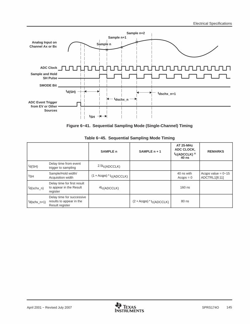
Electrical Specifications
145April 2001 − Revised July 2007 SPRS174O
Analog Input onChannel Ax or Bx
ADC Clock
Sample and HoldSH Pulse
SMODE Bit
tdschx_n
tdschx_n+1
Sample n
Sample n+1Sample n+2
tSH
ADC Event Triggerfrom EV or Other
Sources
td(SH)
Figure 6−41. Sequential Sampling Mode (Single-Channel) Timing
Table 6−45. Sequential Sampling Mode Timing
SAMPLE n SAMPLE n + 1
AT 25-MHz ADC CLOCK,tc(ADCCLK) =
40 ns
REMARKS
td(SH)Delay time from eventtrigger to sampling
2.5tc(ADCCLK)
tSHSample/Hold width/Acquisition width
(1 + Acqps) * tc(ADCCLK)40 ns with Acqps = 0
Acqps value = 0−15ADCTRL1[8:11]
td(schx_n)
Delay time for first resultto appear in the Resultregister
4tc(ADCCLK) 160 ns
td(schx_n+1)
Delay time for successiveresults to appear in theResult register
(2 + Acqps) * tc(ADCCLK) 80 ns
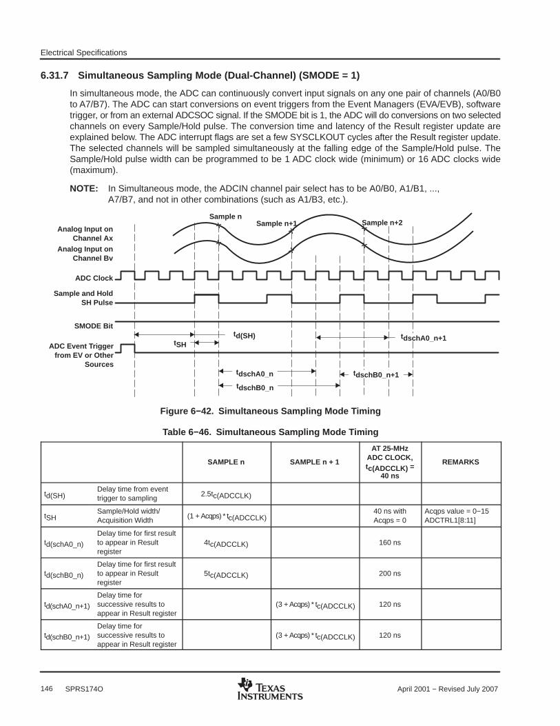
Electrical Specifications
146 April 2001 − Revised July 2007SPRS174O
6.31.7 Simultaneous Sampling Mode (Dual-Channel) (SMODE = 1)
In simultaneous mode, the ADC can continuously convert input signals on any one pair of channels (A0/B0to A7/B7). The ADC can start conversions on event triggers from the Event Managers (EVA/EVB), softwaretrigger, or from an external ADCSOC signal. If the SMODE bit is 1, the ADC will do conversions on two selectedchannels on every Sample/Hold pulse. The conversion time and latency of the Result register update areexplained below. The ADC interrupt flags are set a few SYSCLKOUT cycles after the Result register update.The selected channels will be sampled simultaneously at the falling edge of the Sample/Hold pulse. TheSample/Hold pulse width can be programmed to be 1 ADC clock wide (minimum) or 16 ADC clocks wide(maximum).
NOTE: In Simultaneous mode, the ADCIN channel pair select has to be A0/B0, A1/B1, ...,A7/B7, and not in other combinations (such as A1/B3, etc.).
Analog Input onChannel Ax
Analog Input onChannel Bv
ADC Clock
Sample and HoldSH Pulse
tSH
tdschA0_n
tdschB0_n
tdschB0_n+1
Sample nSample n+1 Sample n+2
tdschA0_n+1td(SH)ADC Event Trigger
from EV or OtherSources
SMODE Bit
Figure 6−42. Simultaneous Sampling Mode Timing
Table 6−46. Simultaneous Sampling Mode Timing
SAMPLE n SAMPLE n + 1
AT 25-MHzADC CLOCK,tc(ADCCLK) =
40 ns
REMARKS
td(SH)Delay time from eventtrigger to sampling
2.5tc(ADCCLK)
tSHSample/Hold width/Acquisition Width
(1 + Acqps) * tc(ADCCLK)40 ns withAcqps = 0
Acqps value = 0−15ADCTRL1[8:11]
td(schA0_n)
Delay time for first resultto appear in Resultregister
4tc(ADCCLK) 160 ns
td(schB0_n)
Delay time for first resultto appear in Resultregister
5tc(ADCCLK) 200 ns
td(schA0_n+1)
Delay time forsuccessive results toappear in Result register
(3 + Acqps) * tc(ADCCLK) 120 ns
td(schB0_n+1)
Delay time forsuccessive results toappear in Result register
(3 + Acqps) * tc(ADCCLK) 120 ns
Electrical Specifications
147April 2001 − Revised July 2007 SPRS174O
6.31.8 Definitions of Specifications and Terminology
Integral Nonlinearity
Integral nonlinearity refers to the deviation of each individual code from a line drawn from zero through fullscale. The point used as zero occurs 1/2 LSB before the first code transition. The full-scale point is definedas level 1/2 LSB beyond the last code transition. The deviation is measured from the center of each particularcode to the true straight line between these two points.
Differential Nonlinearity
An ideal ADC exhibits code transitions that are exactly 1 LSB apart. DNL is the deviation from this ideal value.A differential nonlinearity error of less than ±1 LSB ensures no missing codes.
Zero Offset
The major carry transition should occur when the analog input is at zero volts. Zero error is defined as thedeviation of the actual transition from that point.
Gain Error
The first code transition should occur at an analog value 1/2 LSB above negative full scale. The last transitionshould occur at an analog value 1 1/2 LSB below the nominal full scale. Gain error is the deviation of the actualdifference between first and last code transitions and the ideal difference between first and last codetransitions.
Signal-to-Noise Ratio + Distortion (SINAD)
SINAD is the ratio of the rms value of the measured input signal to the rms sum of all other spectral componentsbelow the Nyquist frequency, including harmonics but excluding dc. The value for SINAD is expressed indecibels.
Effective Number of Bits (ENOB)
For a sine wave, SINAD can be expressed in terms of the number of bits. Using the following formula,
N
(SINAD 1.76)6.02
it is possible to get a measure of performance expressed as N, the effective number of bits. Thus, effectivenumber of bits for a device for sine wave inputs at a given input frequency can be calculated directly from itsmeasured SINAD.
Total Harmonic Distortion (THD)
THD is the ratio of the rms sum of the first six harmonic components to the rms value of the measured inputsignal and is expressed as a percentage or in decibels.
Spurious Free Dynamic Range (SFDR)
SFDR is the difference in dB between the rms amplitude of the input signal and the peak spurious signal.
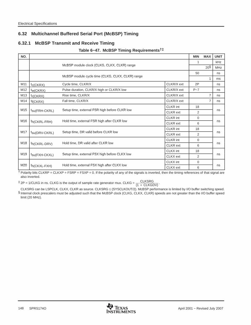
Electrical Specifications
148 April 2001 − Revised July 2007SPRS174O
6.32 Multichannel Buffered Serial Port (McBSP) Timing
6.32.1 McBSP Transmit and Receive Timing
Table 6−47. McBSP Timing Requirements †‡
NO. MIN MAX UNIT
McBSP module clock (CLKG, CLKX, CLKR) range1 kHz
McBSP module clock (CLKG, CLKX, CLKR) range20§ MHz
McBSP module cycle time (CLKG, CLKX, CLKR) range50 ns
McBSP module cycle time (CLKG, CLKX, CLKR) range1 ms
M11 tc(CKRX) Cycle time, CLKR/X CLKR/X ext 2P ns
M12 tw(CKRX) Pulse duration, CLKR/X high or CLKR/X low CLKR/X ext P−7 ns
M13 tr(CKRX) Rise time, CLKR/X CLKR/X ext 7 ns
M14 tf(CKRX) Fall time, CLKR/X CLKR/X ext 7 ns
M15 tsu(FRH-CKRL) Setup time, external FSR high before CLKR lowCLKR int 18
nsM15 tsu(FRH-CKRL) Setup time, external FSR high before CLKR lowCLKR ext 2
ns
M16 th(CKRL-FRH) Hold time, external FSR high after CLKR lowCLKR int 0
nsM16 th(CKRL-FRH) Hold time, external FSR high after CLKR lowCLKR ext 6
ns
M17 tsu(DRV-CKRL) Setup time, DR valid before CLKR lowCLKR int 18
nsM17 tsu(DRV-CKRL) Setup time, DR valid before CLKR lowCLKR ext 2
ns
M18 th(CKRL-DRV) Hold time, DR valid after CLKR lowCLKR int 0
nsM18 th(CKRL-DRV) Hold time, DR valid after CLKR lowCLKR ext 6
ns
M19 tsu(FXH-CKXL) Setup time, external FSX high before CLKX lowCLKX int 18
nsM19 tsu(FXH-CKXL) Setup time, external FSX high before CLKX lowCLKX ext 2
ns
M20 th(CKXL-FXH) Hold time, external FSX high after CLKX lowCLKX int 0
nsM20 th(CKXL-FXH) Hold time, external FSX high after CLKX lowCLKX ext 6
ns
† Polarity bits CLKRP = CLKXP = FSRP = FSXP = 0. If the polarity of any of the signals is inverted, then the timing references of that signal arealso inverted.
‡ 2P = 1/CLKG in ns. CLKG is the output of sample rate generator mux. CLKG = CLKSRG(1 CLKGDV)
.
CLKSRG can be LSPCLK, CLKX, CLKR as source. CLKSRG ≤ (SYSCLKOUT/2). McBSP performance is limited by I/O buffer switching speed.§ Internal clock prescalers must be adjusted such that the McBSP clock (CLKG, CLKX, CLKR) speeds are not greater than the I/O buffer speed
limit (20 MHz).
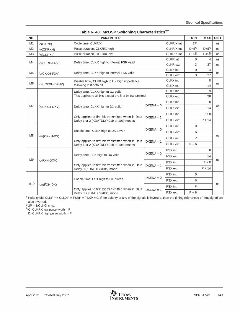
Electrical Specifications
149April 2001 − Revised July 2007 SPRS174O
Table 6−48. McBSP Switching Characteristics †‡
NO. PARAMETER MIN MAX UNIT
M1 tc(CKRX) Cycle time, CLKR/X CLKR/X int 2P ns
M2 tw(CKRXH) Pulse duration, CLKR/X high CLKR/X int D−5§ D+5§ ns
M3 tw(CKRXL) Pulse duration, CLKR/X low CLKR/X int C−5§ C+5§ ns
M4 td(CKRH-FRV) Delay time, CLKR high to internal FSR validCLKR int 0 4 ns
M4 td(CKRH-FRV) Delay time, CLKR high to internal FSR validCLKR ext 3 27 ns
M5 td(CKXH-FXV) Delay time, CLKX high to internal FSX validCLKX int 0 4
nsM5 td(CKXH-FXV) Delay time, CLKX high to internal FSX validCLKX ext 3 27
ns
M6 tdis(CKXH-DXHZ)Disable time, CLKX high to DX high impedance CLKX int 8
nsM6 tdis(CKXH-DXHZ)Disable time, CLKX high to DX high impedance following last data bit CLKX ext 14
ns
Delay time, CLKX high to DX valid. CLKX int 9Delay time, CLKX high to DX valid. This applies to all bits except the first bit transmitted. CLKX ext 28
M7 t DXENA = 0CLKX int 8
nsM7 td(CKXH-DXV) Delay time, CLKX high to DX valid DXENA = 0CLKX ext 14
ns
Only applies to first bit transmitted when in Data DXENA = 1CLKX int P + 8
Only applies to first bit transmitted when in DataDelay 1 or 2 (XDATDLY=01b or 10b) modes
DXENA = 1CLKX ext P + 14
DXENA = 0CLKX int 0
M8 ten(CKXH-DX)
Enable time, CLKX high to DX driven DXENA = 0CLKX ext 6
nsM8 ten(CKXH-DX)
Only applies to first bit transmitted when in Data DXENA = 1CLKX int P
ns
Only applies to first bit transmitted when in DataDelay 1 or 2 (XDATDLY=01b or 10b) modes
DXENA = 1CLKX ext P + 6
DXENA = 0FSX int 8
M9 td(FXH-DXV)
Delay time, FSX high to DX valid DXENA = 0FSX ext 14
nsM9 td(FXH-DXV)
Only applies to first bit transmitted when in Data DXENA = 1FSX int P + 8
ns
Only applies to first bit transmitted when in DataDelay 0 (XDATDLY=00b) mode.
DXENA = 1FSX ext P + 14
DXENA = 0FSX int 0
M10 ten(FXH-DX)
Enable time, FSX high to DX driven DXENA = 0FSX ext 6
nsM10 ten(FXH-DX)
Only applies to first bit transmitted when in Data DXENA = 1FSX int P
ns
Only applies to first bit transmitted when in DataDelay 0 (XDATDLY=00b) mode
DXENA = 1FSX ext P + 6
† Polarity bits CLKRP = CLKXP = FSRP = FSXP = 0. If the polarity of any of the signals is inverted, then the timing references of that signal arealso inverted.
‡ 2P = 1/CLKG in ns.§ C=CLKRX low pulse width = P
D=CLKRX high pulse width = P

Electrical Specifications
150 April 2001 − Revised July 2007SPRS174O
(n−2)Bit (n−1)
(n−3)(n−2)Bit (n−1)
(n−4)(n−3)(n−2)Bit (n−1)
M18M17
M18M17
M17M18
M16M15
M4M4M14
M13M3, M12
M1, M11
M2, M12
(RDATDLY=10b)DR
(RDATDLY=01b)DR
(RDATDLY=00b)DR
FSR (ext)
FSR (int)
CLKR
Figure 6−43. McBSP Receive Timing
M8
M7
M7M8
M6
M7M9
M10
(XDATDLY=10b)DX
(XDATDLY=01b)DX
(XDATDLY=00b)DX
(n−2)Bit (n−1)Bit 0
(n−4)Bit (n−1) (n−3)(n−2)Bit 0
(n−3)(n−2)Bit (n−1)Bit 0
M20
M14M13M3, M12
M1, M11M2, M12
FSX (ext)
FSX (int)
CLKX
M5M5
M19
Figure 6−44. McBSP Transmit Timing
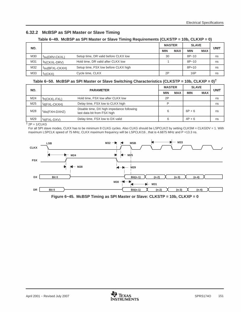
Electrical Specifications
151April 2001 − Revised July 2007 SPRS174O
6.32.2 McBSP as SPI Master or Slave Timing
Table 6−49. McBSP as SPI Master or Slave Timing Requirements (CLKSTP = 10b, CLKXP = 0)
NO.MASTER SLAVE
UNITNO.MIN MAX MIN MAX
UNIT
M30 tsu(DRV-CKXL) Setup time, DR valid before CLKX low 30 8P−10 ns
M31 th(CKXL-DRV) Hold time, DR valid after CLKX low 1 8P−10 ns
M32 tsu(BFXL-CKXH) Setup time, FSX low before CLKX high 8P+10 ns
M33 tc(CKX) Cycle time, CLKX 2P 16P ns
Table 6−50. McBSP as SPI Master or Slave Switching Characteristics (CLKSTP = 10b, CLKXP = 0) †
NO. PARAMETERMASTER SLAVE
UNITNO. PARAMETERMIN MAX MIN MAX
UNIT
M24 th(CKXL-FXL) Hold time, FSX low after CLKX low 2P ns
M25 td(FXL-CKXH) Delay time, FSX low to CLKX high P ns
M28 tdis(FXH-DXHZ)Disable time, DX high impedance followinglast data bit from FSX high
6 6P + 6 ns
M29 td(FXL-DXV) Delay time, FSX low to DX valid 6 4P + 6 ns
† 2P = 1/CLKG For all SPI slave modes, CLKX has to be minimum 8 CLKG cycles. Also CLKG should be LSPCLK/2 by setting CLKSM = CLKGDV = 1. Withmaximum LSPCLK speed of 75 MHz, CLKX maximum frequency will be LSPCLK/16 , that is 4.6875 MHz and P =13.3 ns.
Bit 0 Bit(n-1) (n-2) (n-3) (n-4)
Bit 0 Bit(n-1) (n-2) (n-3) (n-4)
CLKX
FSX
DX
M30M31
DR
M28
M24
M29
M25
LSB MSBM32 M33
Figure 6−45. McBSP Timing as SPI Master or Slave: CLKSTP = 10b, CLKXP = 0
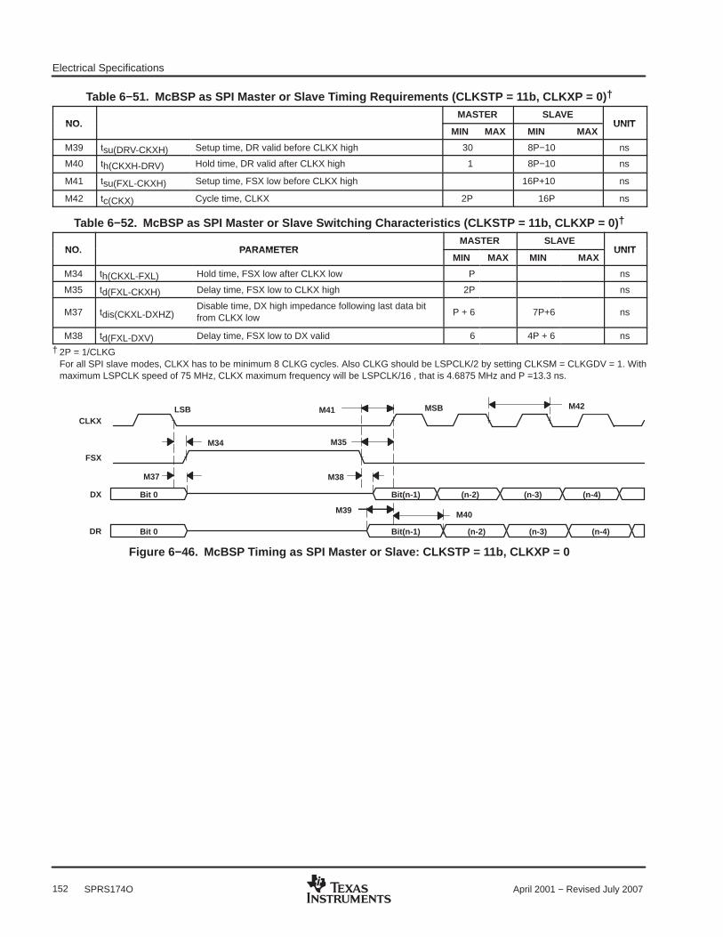
Electrical Specifications
152 April 2001 − Revised July 2007SPRS174O
Table 6−51. McBSP as SPI Master or Slave Timing Requirements (CLKSTP = 11b, CLKXP = 0) †
NO.MASTER SLAVE
UNITNO.MIN MAX MIN MAX
UNIT
M39 tsu(DRV-CKXH) Setup time, DR valid before CLKX high 30 8P−10 ns
M40 th(CKXH-DRV) Hold time, DR valid after CLKX high 1 8P−10 ns
M41 tsu(FXL-CKXH) Setup time, FSX low before CLKX high 16P+10 ns
M42 tc(CKX) Cycle time, CLKX 2P 16P ns
Table 6−52. McBSP as SPI Master or Slave Switching Characteristics (CLKSTP = 11b, CLKXP = 0) †
NO. PARAMETERMASTER SLAVE
UNITNO. PARAMETERMIN MAX MIN MAX
UNIT
M34 th(CKXL-FXL) Hold time, FSX low after CLKX low P ns
M35 td(FXL-CKXH) Delay time, FSX low to CLKX high 2P ns
M37 tdis(CKXL-DXHZ)Disable time, DX high impedance following last data bitfrom CLKX low
P + 6 7P+6 ns
M38 td(FXL-DXV) Delay time, FSX low to DX valid 6 4P + 6 ns
† 2P = 1/CLKG For all SPI slave modes, CLKX has to be minimum 8 CLKG cycles. Also CLKG should be LSPCLK/2 by setting CLKSM = CLKGDV = 1. Withmaximum LSPCLK speed of 75 MHz, CLKX maximum frequency will be LSPCLK/16 , that is 4.6875 MHz and P =13.3 ns.
Bit 0 Bit(n-1) (n-2) (n-3) (n-4)
Bit 0 Bit(n-1) (n-2) (n-3) (n-4)
CLKX
FSX
DX
DR
M35
M37
M40M39
M38
M34
LSB MSBM41 M42
Figure 6−46. McBSP Timing as SPI Master or Slave: CLKSTP = 11b, CLKXP = 0
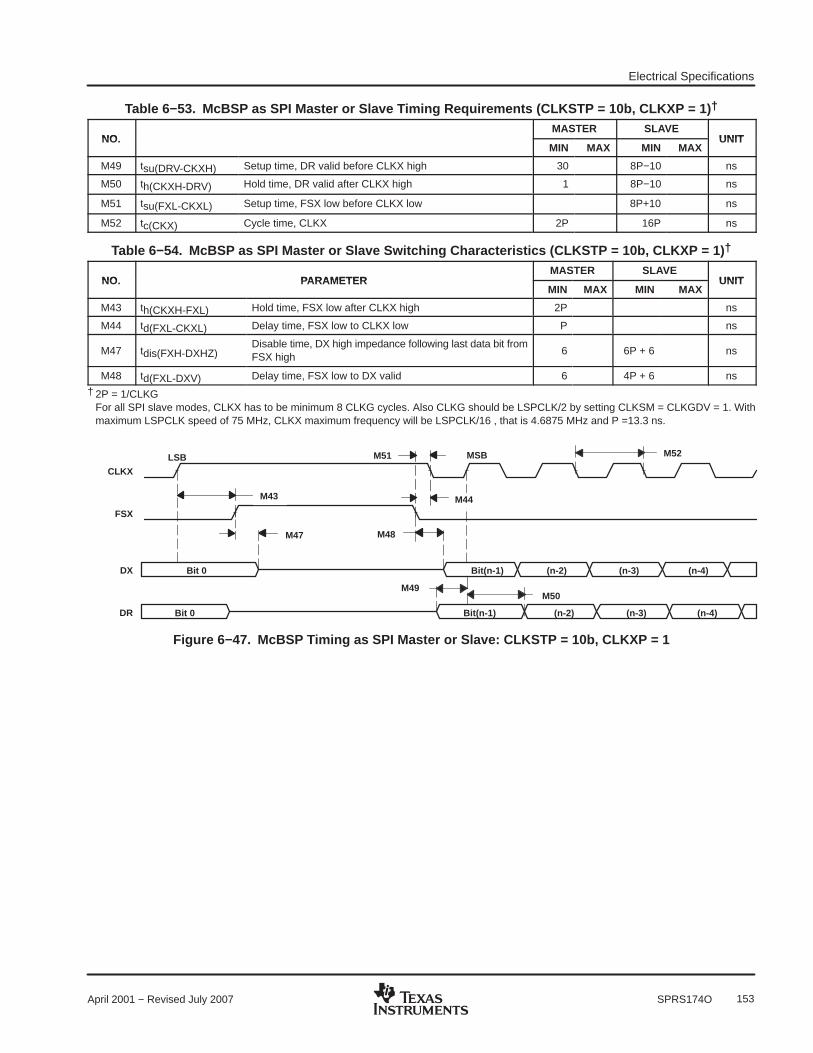
Electrical Specifications
153April 2001 − Revised July 2007 SPRS174O
Table 6−53. McBSP as SPI Master or Slave Timing Requirements (CLKSTP = 10b, CLKXP = 1) †
NO.MASTER SLAVE
UNITNO.MIN MAX MIN MAX
UNIT
M49 tsu(DRV-CKXH) Setup time, DR valid before CLKX high 30 8P−10 ns
M50 th(CKXH-DRV) Hold time, DR valid after CLKX high 1 8P−10 ns
M51 tsu(FXL-CKXL) Setup time, FSX low before CLKX low 8P+10 ns
M52 tc(CKX) Cycle time, CLKX 2P 16P ns
Table 6−54. McBSP as SPI Master or Slave Switching Characteristics (CLKSTP = 10b, CLKXP = 1) †
NO. PARAMETERMASTER SLAVE
UNITNO. PARAMETERMIN MAX MIN MAX
UNIT
M43 th(CKXH-FXL) Hold time, FSX low after CLKX high 2P ns
M44 td(FXL-CKXL) Delay time, FSX low to CLKX low P ns
M47 tdis(FXH-DXHZ)Disable time, DX high impedance following last data bit fromFSX high
6 6P + 6 ns
M48 td(FXL-DXV) Delay time, FSX low to DX valid 6 4P + 6 ns
† 2P = 1/CLKG For all SPI slave modes, CLKX has to be minimum 8 CLKG cycles. Also CLKG should be LSPCLK/2 by setting CLKSM = CLKGDV = 1. Withmaximum LSPCLK speed of 75 MHz, CLKX maximum frequency will be LSPCLK/16 , that is 4.6875 MHz and P =13.3 ns.
M51
M50
M47
Bit 0 Bit(n-1) (n-2) (n-3) (n-4)
Bit 0 Bit(n-1) (n-2) (n-3) (n-4)
CLKX
FSX
DX
DR
M44
M48
M49
M43
LSB MSB M52
Figure 6−47. McBSP Timing as SPI Master or Slave: CLKSTP = 10b, CLKXP = 1
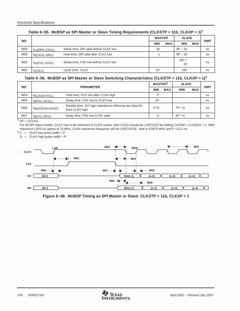
Electrical Specifications
154 April 2001 − Revised July 2007SPRS174O
Table 6−55. McBSP as SPI Master or Slave Timing Requirements (CLKSTP = 11b, CLKXP = 1) †
NO.MASTER SLAVE
UNITNO.MIN MAX MIN MAX
UNIT
M58 tsu(DRV-CKXL) Setup time, DR valid before CLKX low 30 8P − 10 ns
M59 th(CKXL-DRV) Hold time, DR valid after CLKX low 1 8P − 10 ns
M60 tsu(FXL-CKXL) Setup time, FSX low before CLKX low16P +
10ns
M61 tc(CKX) Cycle time, CLKX 2P 16P ns
Table 6−56. McBSP as SPI Master or Slave Switching Characteristics (CLKSTP = 11b, CLKXP = 1) †
NO. PARAMETERMASTER‡ SLAVE
UNITNO. PARAMETERMIN MAX MIN MAX
UNIT
M53 th(CKXH-FXL) Hold time, FSX low after CLKX high P ns
M54 td(FXL-CKXL) Delay time, FSX low to CLKX low 2P ns
M56 tdis(CKXH-DXHZ)Disable time, DX high impedance following last data bitfrom CLKX high
P+6 7P + 6 ns
M57 td(FXL-DXV) Delay time, FSX low to DX valid 6 4P + 6 ns
† 2P = 1/CLKG For all SPI slave modes, CLKX has to be minimum 8 CLKG cycles. Also CLKG should be LSPCLK/2 by setting CLKSM = CLKGDV = 1. Withmaximum LSPCLK speed of 75 MHz, CLKX maximum frequency will be LSPCLK/16 , that is 4.6875 MHz and P =13.3 ns.
‡ C = CLKX low pulse width = PD = CLKX high pulse width = P
Bit 0 Bit(n-1) (n-2) (n-3) (n-4)
Bit 0 Bit(n-1) (n-2) (n-3) (n-4)
CLKX
FSX
DX
DR
M54
M58
M56
M53
M55
M59
M57
LSB MSBM60 M61
Figure 6−48. McBSP Timing as SPI Master or Slave: CLKSTP = 11b, CLKXP = 1

Electrical Specifications
155April 2001 − Revised July 2007 SPRS174O
6.33 Flash Timing (F281x Only)
6.33.1 Recommended Operating ConditionsMIN NOM MAX UNIT
Nf Flash endurance for the array (Write/erase cycles) 0°C to 85°C (ambient) 100 1000 cycles
NOTP OTP endurance for the array (Write cycles) 0°C to 85°C (ambient) 1 write
Table 6−57. Flash Parameters at 150-MHz SYSCLKOUT †
PARAMETER MIN TYP MAX UNIT
16-Bit WordUsing Flash API v1‡ 35 µs
16-Bit WordUsing Flash API v2.10 50 µs
Program Time 8K SectorUsing Flash API v1‡ 170 ms
Program Time 8K SectorUsing Flash API v2.10 250 ms
16K SectorUsing Flash API v1‡ 320 ms
16K SectorUsing Flash API v2.10 500 ms
Erase Time8K Sector 10 s
Erase Time16K Sector 11 s
IDD3VFLP VDD3VFL current consumption during the Erase/Program cycleErase 75 mA
IDD3VFLP VDD3VFL current consumption during the Erase/Program cycleProgram 35 mA
IDDP VDD current consumption during Erase/Program cycle 140 mA
IDDIOP VDDIO current consumption during Erase/Program cycle 20 mA
† Typical parameters as seen at room temperature including function call overhead.‡ Flash API v1.00 is useable on rev. C silicon only.
Table 6−58. Flash/OTP Access Timing
PARAMETER MIN MAX UNIT
ta(fp) Paged Flash access time 36 ns
ta(fr) Random Flash access time 36 ns
ta(OTP) OTP access time 60 ns

Electrical Specifications
156 April 2001 − Revised July 2007SPRS174O
Table 6−59. Minimum Required Flash Wait-States at Different Frequencies (F281x devices)
SYSCLKOUT (MHz) SYSCLKOUT (ns) PAGE WAIT-STATE † RANDOM WAITSTATE†‡ OTP
150 6.67 5 5 8
120 8.33 4 4 7
100 10 3 3 5
75 13.33 2 2 4
50 20 1 1 2
30 33.33 1 1 1
25 40 0 1 1
15 66.67 0 1 1
4 250 0 1 1† Formulas to compute page wait state and random wait state:
Flash Page Wait State ta(fp)
tc(SCO) 1 (round up to the next highest integer), or 0 whichever is larger
Flash Random Wait State ta(fr)
tc(SCO) 1 (round up to the next highest integer), or 1 whichever is larger
OTP Wait State ta(OTP)
tc(SCO) 1 (round up to the next highest integer), or 1 whichever is larger
‡ Random wait state must be greater than or equal to 1
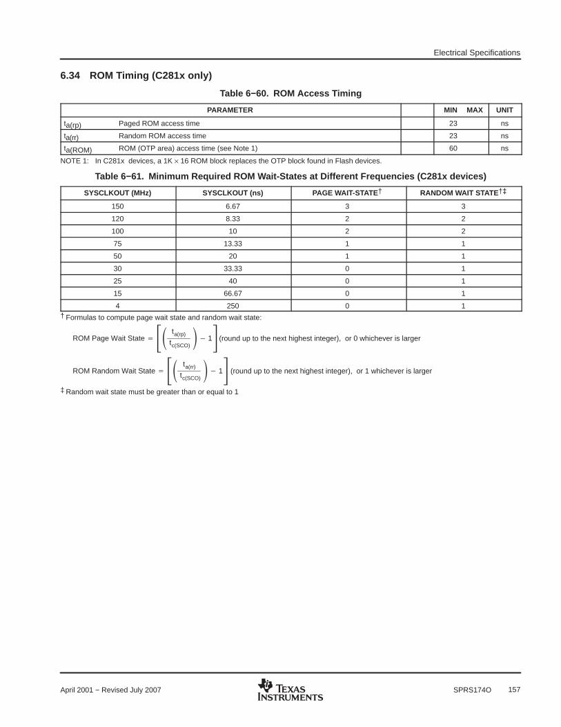
Electrical Specifications
157April 2001 − Revised July 2007 SPRS174O
6.34 ROM Timing (C281x only)
Table 6−60. ROM Access Timing
PARAMETER MIN MAX UNIT
ta(rp) Paged ROM access time 23 ns
ta(rr) Random ROM access time 23 ns
ta(ROM) ROM (OTP area) access time (see Note 1) 60 ns
NOTE 1: In C281x devices, a 1K × 16 ROM block replaces the OTP block found in Flash devices.
Table 6−61. Minimum Required ROM Wait-States at Different Frequencies (C281x devices)
SYSCLKOUT (MHz) SYSCLKOUT (ns) PAGE WAIT-STATE † RANDOM WAIT STATE †‡
150 6.67 3 3
120 8.33 2 2
100 10 2 2
75 13.33 1 1
50 20 1 1
30 33.33 0 1
25 40 0 1
15 66.67 0 1
4 250 0 1† Formulas to compute page wait state and random wait state:
ROM Page Wait State ta(rp)
tc(SCO) 1 (round up to the next highest integer), or 0 whichever is larger
ROM Random Wait State ta(rr)
tc(SCO) 1 (round up to the next highest integer), or 1 whichever is larger
‡ Random wait state must be greater than or equal to 1
Electrical Specifications
158 April 2001 − Revised July 2007SPRS174O
6.35 Migrating From F281x Devices to C281x Devices
The migration issues to be considered while migrating from the F281x devices to C281x devices are asfollows:
• The 1K OTP memory available in F281x devices has been replaced by 1K ROM C281x devices.
• Power sequencing is not needed for C281x devices. In other words, 3.3-V and 1.8-V (or 1.9-V) can ramptogether. C281x can also be used on boards that have F281x power sequencing implemented; however,if the 1.8-V (or 1.9-V) rail lags the 3.3-V rail, the GPIO pins are undefined until the 1.8-V rail reaches atleast 1 V.
• Current consumption differs for F281x and C281x devices for all four possible modes. See the appropriateelectrical section for exact numbers.
• The VDD3VFL pin is the 3.3-V flash core power pin in F281x devices but is a VDDIO pin in C281x devices.
• F281x and C281x devices are pin-compatible and code-compatible; however, they are electricallydifferent with different EMI/ESD profiles. Before ramping production with c281x devices, evaluateperformance of the hardware design with both devices
• Addresses 0x3D7BFC through 0x3D7BFF in the OTP and addresses 0x3F7FF2 through 0x3F7FF5 in themain ROM array are reserved for ROM part-specific information and are not available for userapplications.
• The ADC module in C281x devices can operate at 24.9k bias on ADCRESEXT pin for the full range1−25MHz. While migrating the F281x designs to C281x, use a 24.9k resistor for biasing the ADC.
• The paged and random wait-state specifications for the flash and ROM parts are different. While migratingfrom flash to ROM parts, the same wait-state values must be used for best performance compatibility (forexample, in applications that use software delay loops or where precise interrupt latencies are critical).
• The PART−ID register value is different for Flash and ROM parts.
For errata applicable to 281x devices, see the TMS320F2810, TMS320F2811, TMS320F2812,TMS320C2810, TMS320C2811, TMS320C2812 Digital Signal Processors Silicon Errata (literature numberSPRZ193).
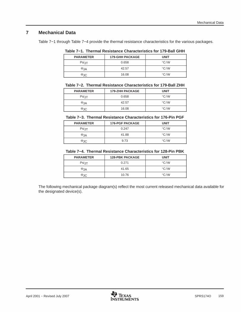
Mechanical Data
159April 2001 − Revised July 2007 SPRS174O
7 Mechanical Data
Table 7−1 through Table 7−4 provide the thermal resistance characteristics for the various packages.
Table 7−1. Thermal Resistance Characteristics for 179-Ball GHHPARAMETER 179-GHH PACKAGE UNIT
PsiJT 0.658 °C/W
ΘJA 42.57 °C/W
ΘJC 16.08 °C/W
Table 7−2. Thermal Resistance Characteristics for 179-Ball ZHHPARAMETER 179-ZHH PACKAGE UNIT
PsiJT 0.658 °C/W
ΘJA 42.57 °C/W
ΘJC 16.08 °C/W
Table 7−3. Thermal Resistance Characteristics for 176-Pin PGFPARAMETER 176-PGF PACKAGE UNIT
PsiJT 0.247 °C/W
ΘJA 41.88 °C/W
ΘJC 9.73 °C/W
Table 7−4. Thermal Resistance Characteristics for 128-Pin PBKPARAMETER 128-PBK PACKAGE UNIT
PsiJT 0.271 °C/W
ΘJA 41.65 °C/W
ΘJC 10.76 °C/W
The following mechanical package diagram(s) reflect the most current released mechanical data available forthe designated device(s).

PACKAGING INFORMATION
Orderable Device Status (1) PackageType
PackageDrawing
Pins PackageQty
Eco Plan (2) Lead/Ball Finish MSL Peak Temp (3)
TMS320F2810PBKA ACTIVE LQFP PBK 128 90 Green (RoHS &no Sb/Br)
CU NIPDAU Level-2-260C-1 YEAR
TMS320F2810PBKQ ACTIVE LQFP PBK 128 90 Green (RoHS &no Sb/Br)
CU NIPDAU Level-2-260C-1 YEAR
TMS320F2810PBKS ACTIVE LQFP PBK 128 90 Green (RoHS &no Sb/Br)
CU NIPDAU Level-2-260C-1 YEAR
TMS320F2811PBKA ACTIVE LQFP PBK 128 90 Green (RoHS &no Sb/Br)
CU NIPDAU Level-2-260C-1 YEAR
TMS320F2811PBKQ ACTIVE LQFP PBK 128 90 Green (RoHS &no Sb/Br)
CU NIPDAU Level-2-260C-1 YEAR
TMS320F2811PBKS ACTIVE LQFP PBK 128 90 Green (RoHS &no Sb/Br)
CU NIPDAU Level-2-260C-1 YEAR
TMS320F2812GHHA ACTIVE BGA GHH 179 160 TBD SNPB Level-3-220C-168 HR
TMS320F2812GHHAR ACTIVE BGA GHH 179 1000 TBD SNPB Level-3-220C-168 HR
TMS320F2812GHHQ ACTIVE BGA GHH 179 160 TBD SNPB Level-3-220C-168 HR
TMS320F2812GHHS ACTIVE BGA GHH 179 160 TBD SNPB Level-3-220C-168 HR
TMS320F2812PGFA ACTIVE LQFP PGF 176 40 Green (RoHS &no Sb/Br)
CU NIPDAU Level-3-260C-168 HR
TMS320F2812PGFQ ACTIVE LQFP PGF 176 40 Green (RoHS &no Sb/Br)
CU NIPDAU Level-3-260C-168 HR
TMS320F2812PGFS ACTIVE LQFP PGF 176 40 Green (RoHS &no Sb/Br)
CU NIPDAU Level-3-260C-168 HR
TMS320F2812ZHHA ACTIVE BGA MI CROSTA
R
ZHH 179 160 Green (RoHS &no Sb/Br)
SNAGCU Level-3-260C-168 HR
TMS320F2812ZHHS ACTIVE BGA MI CROSTA
R
ZHH 179 160 Green (RoHS &no Sb/Br)
SNAGCU Level-3-260C-168 HR
(1) The marketing status values are defined as follows:ACTIVE: Product device recommended for new designs.LIFEBUY: TI has announced that the device will be discontinued, and a lifetime-buy period is in effect.NRND: Not recommended for new designs. Device is in production to support existing customers, but TI does not recommend using this part ina new design.PREVIEW: Device has been announced but is not in production. Samples may or may not be available.OBSOLETE: TI has discontinued the production of the device.
(2) Eco Plan - The planned eco-friendly classification: Pb-Free (RoHS), Pb-Free (RoHS Exempt), or Green (RoHS & no Sb/Br) - please checkhttp://www.ti.com/productcontent for the latest availability information and additional product content details.TBD: The Pb-Free/Green conversion plan has not been defined.Pb-Free (RoHS): TI's terms "Lead-Free" or "Pb-Free" mean semiconductor products that are compatible with the current RoHS requirementsfor all 6 substances, including the requirement that lead not exceed 0.1% by weight in homogeneous materials. Where designed to be solderedat high temperatures, TI Pb-Free products are suitable for use in specified lead-free processes.Pb-Free (RoHS Exempt): This component has a RoHS exemption for either 1) lead-based flip-chip solder bumps used between the die andpackage, or 2) lead-based die adhesive used between the die and leadframe. The component is otherwise considered Pb-Free (RoHScompatible) as defined above.Green (RoHS & no Sb/Br): TI defines "Green" to mean Pb-Free (RoHS compatible), and free of Bromine (Br) and Antimony (Sb) based flameretardants (Br or Sb do not exceed 0.1% by weight in homogeneous material)
(3) MSL, Peak Temp. -- The Moisture Sensitivity Level rating according to the JEDEC industry standard classifications, and peak soldertemperature.
Important Information and Disclaimer:The information provided on this page represents TI's knowledge and belief as of the date that it is
PACKAGE OPTION ADDENDUM
www.ti.com 11-Jun-2007
Addendum-Page 1

provided. TI bases its knowledge and belief on information provided by third parties, and makes no representation or warranty as to theaccuracy of such information. Efforts are underway to better integrate information from third parties. TI has taken and continues to takereasonable steps to provide representative and accurate information but may not have conducted destructive testing or chemical analysis onincoming materials and chemicals. TI and TI suppliers consider certain information to be proprietary, and thus CAS numbers and other limitedinformation may not be available for release.
In no event shall TI's liability arising out of such information exceed the total purchase price of the TI part(s) at issue in this document sold by TIto Customer on an annual basis.
PACKAGE OPTION ADDENDUM
www.ti.com 11-Jun-2007
Addendum-Page 2


MECHANICAL DATA
MTQF015A – JANUARY 1995 – REVISED DECEMBER 1996
2–1POST OFFICE BOX 655303 • DALLAS, TEXAS 75265POST OFFICE BOX 1443 • HOUSTON, TEXAS 77251–1443
PBK (S-PQFP-G128) PLASTIC QUAD FLATPACK
4040279-3/C 11/96
64
33
Gage Plane
0,13 NOM
0,25
0,450,75
Seating Plane
0,05 MIN
0,23
65
32
96
1
12,40 TYP
0,13
97
128
SQ
SQ
13,80
16,2015,80
1,60 MAX
1,451,35
14,20
0°–7°
0,08
0,40 M0,07
NOTES: A. All linear dimensions are in millimeters.B. This drawing is subject to change without notice.C. Falls within JEDEC MS-026

OCTOBER 1994
1POST OFFICE BOX 655303 • DALLAS, TEXAS 75265
PGF (S-PQFP-G176) PLASTIC QUAD FLATPACK
0,13 NOM
89
0,170,27
88
45
0,45
0,25
0,75
44
Seating Plane
0,05 MIN
4040134/B 03/95
Gage Plane
132
133
176
SQ24,20
SQ25,8026,20
23,80
21,50 SQ1
1,451,35
1,60 MAX
M0,08
0,50
0,08
0°−7°
NOTES: A. All linear dimensions are in millimeters.B. This drawing is subject to change without notice.C. Falls within JEDEC MO-136

PACKAGING INFORMATION
Orderable Device Status (1) PackageType
PackageDrawing
Pins PackageQty
Eco Plan (2) Lead/Ball Finish MSL Peak Temp (3)
TMP320F2811PBKA OBSOLETE LQFP PBK 128 TBD Call TI Call TI
TMS320C2810PBKA ACTIVE LQFP PBK 128 TBD Call TI Call TI
TMS320C2810PBKQ ACTIVE LQFP PBK 128 TBD Call TI Call TI
TMS320C2811PBKA ACTIVE LQFP PBK 128 TBD Call TI Call TI
TMS320C2811PBKQ ACTIVE LQFP PBK 128 TBD Call TI Call TI
TMS320C2812PGFQ ACTIVE LQFP PGF 176 TBD Call TI Call TI
TMS320C2812ZHHA ACTIVE BGA MI CROSTA
R
ZHH 179 TBD Call TI Call TI
TMS320C2812ZHHQ ACTIVE BGA MI CROSTA
R
ZHH 179 TBD Call TI Call TI
TMS320F2810PBKA ACTIVE LQFP PBK 128 90 Green (RoHS &no Sb/Br)
CU NIPDAU Level-2-260C-1 YEAR
TMS320F2810PBKQ ACTIVE LQFP PBK 128 90 Green (RoHS &no Sb/Br)
CU NIPDAU Level-2-260C-1 YEAR
TMS320F2810PBKS ACTIVE LQFP PBK 128 90 Green (RoHS &no Sb/Br)
CU NIPDAU Level-2-260C-1 YEAR
TMS320F2811PBKA ACTIVE LQFP PBK 128 90 Green (RoHS &no Sb/Br)
CU NIPDAU Level-2-260C-1 YEAR
TMS320F2811PBKQ ACTIVE LQFP PBK 128 90 Green (RoHS &no Sb/Br)
CU NIPDAU Level-2-260C-1 YEAR
TMS320F2811PBKS ACTIVE LQFP PBK 128 90 Green (RoHS &no Sb/Br)
CU NIPDAU Level-2-260C-1 YEAR
TMS320F2812GHHA ACTIVE BGA MI CROSTA
R
GHH 179 160 TBD SNPB Level-3-220C-168 HR
TMS320F2812GHHAR ACTIVE BGA MI CROSTA
R
GHH 179 1000 TBD SNPB Level-3-220C-168 HR
TMS320F2812GHHQ ACTIVE BGA MI CROSTA
R
GHH 179 160 TBD SNPB Level-3-220C-168 HR
TMS320F2812GHHS ACTIVE BGA MI CROSTA
R
GHH 179 160 TBD SNPB Level-3-220C-168 HR
TMS320F2812PGFA ACTIVE LQFP PGF 176 40 Green (RoHS &no Sb/Br)
CU NIPDAU Level-3-260C-168 HR
TMS320F2812PGFQ ACTIVE LQFP PGF 176 40 Green (RoHS &no Sb/Br)
CU NIPDAU Level-3-260C-168 HR
TMS320F2812PGFS ACTIVE LQFP PGF 176 40 Green (RoHS &no Sb/Br)
CU NIPDAU Level-3-260C-168 HR
TMS320F2812ZHHA ACTIVE BGA MI CROSTA
R
ZHH 179 160 Green (RoHS &no Sb/Br)
SNAGCU Level-3-260C-168 HR
TMS320F2812ZHHS ACTIVE BGA MI CROSTA
R
ZHH 179 160 Green (RoHS &no Sb/Br)
SNAGCU Level-3-260C-168 HR
TYCOF2812PGFA ACTIVE LQFP PGF 176 40 Green (RoHS &no Sb/Br)
CU NIPDAU Level-3-260C-168 HR
PACKAGE OPTION ADDENDUM
www.ti.com 4-May-2009
Addendum-Page 1

(1) The marketing status values are defined as follows:ACTIVE: Product device recommended for new designs.LIFEBUY: TI has announced that the device will be discontinued, and a lifetime-buy period is in effect.NRND: Not recommended for new designs. Device is in production to support existing customers, but TI does not recommend using this part ina new design.PREVIEW: Device has been announced but is not in production. Samples may or may not be available.OBSOLETE: TI has discontinued the production of the device.
(2) Eco Plan - The planned eco-friendly classification: Pb-Free (RoHS), Pb-Free (RoHS Exempt), or Green (RoHS & no Sb/Br) - please checkhttp://www.ti.com/productcontent for the latest availability information and additional product content details.TBD: The Pb-Free/Green conversion plan has not been defined.Pb-Free (RoHS): TI's terms "Lead-Free" or "Pb-Free" mean semiconductor products that are compatible with the current RoHS requirementsfor all 6 substances, including the requirement that lead not exceed 0.1% by weight in homogeneous materials. Where designed to be solderedat high temperatures, TI Pb-Free products are suitable for use in specified lead-free processes.Pb-Free (RoHS Exempt): This component has a RoHS exemption for either 1) lead-based flip-chip solder bumps used between the die andpackage, or 2) lead-based die adhesive used between the die and leadframe. The component is otherwise considered Pb-Free (RoHScompatible) as defined above.Green (RoHS & no Sb/Br): TI defines "Green" to mean Pb-Free (RoHS compatible), and free of Bromine (Br) and Antimony (Sb) based flameretardants (Br or Sb do not exceed 0.1% by weight in homogeneous material)
(3) MSL, Peak Temp. -- The Moisture Sensitivity Level rating according to the JEDEC industry standard classifications, and peak soldertemperature.
Important Information and Disclaimer:The information provided on this page represents TI's knowledge and belief as of the date that it isprovided. TI bases its knowledge and belief on information provided by third parties, and makes no representation or warranty as to theaccuracy of such information. Efforts are underway to better integrate information from third parties. TI has taken and continues to takereasonable steps to provide representative and accurate information but may not have conducted destructive testing or chemical analysis onincoming materials and chemicals. TI and TI suppliers consider certain information to be proprietary, and thus CAS numbers and other limitedinformation may not be available for release.
In no event shall TI's liability arising out of such information exceed the total purchase price of the TI part(s) at issue in this document sold by TIto Customer on an annual basis.
OTHER QUALIFIED VERSIONS OF TMS320F2812 :
• Catalog: SM320F2812
• Enhanced Product: SM320F2812-EP
• Military: SMJ320F2812
NOTE: Qualified Version Definitions:
• Catalog - TI's standard catalog product
• Enhanced Product - Supports Defense, Aerospace and Medical Applications
• Military - QML certified for Military and Defense Applications
PACKAGE OPTION ADDENDUM
www.ti.com 4-May-2009
Addendum-Page 2

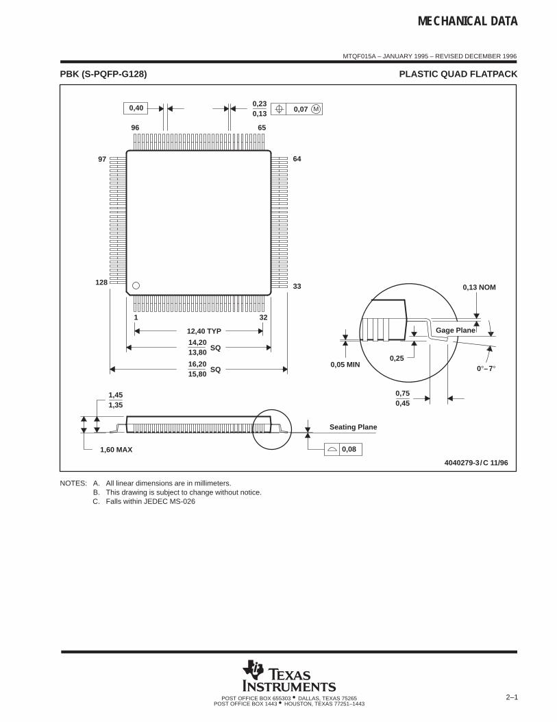
MECHANICAL DATA
MTQF015A – JANUARY 1995 – REVISED DECEMBER 1996
2–1POST OFFICE BOX 655303 • DALLAS, TEXAS 75265POST OFFICE BOX 1443 • HOUSTON, TEXAS 77251–1443
PBK (S-PQFP-G128) PLASTIC QUAD FLATPACK
4040279-3/C 11/96
64
33
Gage Plane
0,13 NOM
0,25
0,450,75
Seating Plane
0,05 MIN
0,23
65
32
96
1
12,40 TYP
0,13
97
128
SQ
SQ
13,80
16,2015,80
1,60 MAX
1,451,35
14,20
0°–7°
0,08
0,40 M0,07
NOTES: A. All linear dimensions are in millimeters.B. This drawing is subject to change without notice.C. Falls within JEDEC MS-026

OCTOBER 1994
1POST OFFICE BOX 655303 • DALLAS, TEXAS 75265
PGF (S-PQFP-G176) PLASTIC QUAD FLATPACK
0,13 NOM
89
0,170,27
88
45
0,45
0,25
0,75
44
Seating Plane
0,05 MIN
4040134/B 03/95
Gage Plane
132
133
176
SQ24,20
SQ25,8026,20
23,80
21,50 SQ1
1,451,35
1,60 MAX
M0,08
0,50
0,08
0°−7°
NOTES: A. All linear dimensions are in millimeters.B. This drawing is subject to change without notice.C. Falls within JEDEC MO-136


IMPORTANT NOTICETexas Instruments Incorporated and its subsidiaries (TI) reserve the right to make corrections, modifications, enhancements, improvements,and other changes to its products and services at any time and to discontinue any product or service without notice. Customers shouldobtain the latest relevant information before placing orders and should verify that such information is current and complete. All products aresold subject to TI’s terms and conditions of sale supplied at the time of order acknowledgment.TI warrants performance of its hardware products to the specifications applicable at the time of sale in accordance with TI’s standardwarranty. Testing and other quality control techniques are used to the extent TI deems necessary to support this warranty. Except wheremandated by government requirements, testing of all parameters of each product is not necessarily performed.TI assumes no liability for applications assistance or customer product design. Customers are responsible for their products andapplications using TI components. To minimize the risks associated with customer products and applications, customers should provideadequate design and operating safeguards.TI does not warrant or represent that any license, either express or implied, is granted under any TI patent right, copyright, mask work right,or other TI intellectual property right relating to any combination, machine, or process in which TI products or services are used. Informationpublished by TI regarding third-party products or services does not constitute a license from TI to use such products or services or awarranty or endorsement thereof. Use of such information may require a license from a third party under the patents or other intellectualproperty of the third party, or a license from TI under the patents or other intellectual property of TI.Reproduction of TI information in TI data books or data sheets is permissible only if reproduction is without alteration and is accompaniedby all associated warranties, conditions, limitations, and notices. Reproduction of this information with alteration is an unfair and deceptivebusiness practice. TI is not responsible or liable for such altered documentation. Information of third parties may be subject to additionalrestrictions.Resale of TI products or services with statements different from or beyond the parameters stated by TI for that product or service voids allexpress and any implied warranties for the associated TI product or service and is an unfair and deceptive business practice. TI is notresponsible or liable for any such statements.TI products are not authorized for use in safety-critical applications (such as life support) where a failure of the TI product would reasonablybe expected to cause severe personal injury or death, unless officers of the parties have executed an agreement specifically governingsuch use. Buyers represent that they have all necessary expertise in the safety and regulatory ramifications of their applications, andacknowledge and agree that they are solely responsible for all legal, regulatory and safety-related requirements concerning their productsand any use of TI products in such safety-critical applications, notwithstanding any applications-related information or support that may beprovided by TI. Further, Buyers must fully indemnify TI and its representatives against any damages arising out of the use of TI products insuch safety-critical applications.TI products are neither designed nor intended for use in military/aerospace applications or environments unless the TI products arespecifically designated by TI as military-grade or "enhanced plastic." Only products designated by TI as military-grade meet militaryspecifications. Buyers acknowledge and agree that any such use of TI products which TI has not designated as military-grade is solely atthe Buyer's risk, and that they are solely responsible for compliance with all legal and regulatory requirements in connection with such use.TI products are neither designed nor intended for use in automotive applications or environments unless the specific TI products aredesignated by TI as compliant with ISO/TS 16949 requirements. Buyers acknowledge and agree that, if they use any non-designatedproducts in automotive applications, TI will not be responsible for any failure to meet such requirements.Following are URLs where you can obtain information on other Texas Instruments products and application solutions:Products ApplicationsAmplifiers amplifier.ti.com Audio www.ti.com/audioData Converters dataconverter.ti.com Automotive www.ti.com/automotiveDLP® Products www.dlp.com Broadband www.ti.com/broadbandDSP dsp.ti.com Digital Control www.ti.com/digitalcontrolClocks and Timers www.ti.com/clocks Medical www.ti.com/medicalInterface interface.ti.com Military www.ti.com/militaryLogic logic.ti.com Optical Networking www.ti.com/opticalnetworkPower Mgmt power.ti.com Security www.ti.com/securityMicrocontrollers microcontroller.ti.com Telephony www.ti.com/telephonyRFID www.ti-rfid.com Video & Imaging www.ti.com/videoRF/IF and ZigBee® Solutions www.ti.com/lprf Wireless www.ti.com/wireless
Mailing Address: Texas Instruments, Post Office Box 655303, Dallas, Texas 75265Copyright © 2009, Texas Instruments Incorporated