tlc227x-q1 advanced lincmos™ rail-to-rail … from revision d (march 2009) to revision e page •...
TRANSCRIPT
|VDD ±| − Supply Voltage (V)
10
8
6
4
12
14
16
TA = 25°C
IO = ±50 µA
IO = ±500 µA
V(O
PP
)−
Ma
xim
um
Pe
ak-t
o-P
ea
k O
utp
ut
Vo
lta
ge
(V
)V
O(P
P)
4 6 8 10 12 14 16
Product
Folder
Sample &Buy
Technical
Documents
Tools &
Software
Support &Community
An IMPORTANT NOTICE at the end of this data sheet addresses availability, warranty, changes, use in safety-critical applications,intellectual property matters and other important disclaimers. PRODUCTION DATA.
TLC2272-Q1, TLC2272A-Q1, TLC2274-Q1, TLC2274A-Q1SGLS007F –FEBRUARY 2003–REVISED MARCH 2016
TLC227x-Q1 Advanced LinCMOS™ Rail-To-Rail Operational Amplifiers
1
1 Features1• Qualified for Automotive Applications
– Device Temperature Grade: –40°C to 125°CAmbient Operating Temperature Range
– Device HBM ESD Classification Level 2– Device CDM ESD Classification Level C6
• Output Swing Includes Both Supply Rails• Low Noise: 9 nV/√Hz Typical at f = 1 kHz• Low Input Bias Current: 1 pA Typical• Fully Specified for Both Single-Supply and Split-
Supply Operation• Common-Mode Input Voltage Range Includes
Negative Rail• High-Gain Bandwidth: 2.2 MHz Typical• High Slew Rate: 3.6 V/μs Typical• Low Input Offset Voltage 950 μV Maximum at
TA = 25°C• Macromodel Included
2 Applications• Gear Boxes• Transmission Control• On-Board Chargers• Body Control Modules• Steering Angle Sensors• Electric Power Steering• Engine Control Units• Airbags• Blind Spot Detection• Clusters• Car Audio• Navigation Systems• White Goods (Refrigerators, Washing Machines)
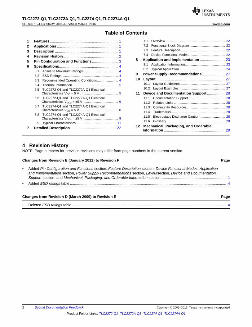
3 DescriptionThe TLC2272-Q1 and TLC2274-Q1 devices are dualand quadruple operational amplifiers from TexasInstruments. Both devices exhibit rail-to-rail outputperformance for increased dynamic range in single-or split-supply applications. The TLC227x-Q1 familyoffers 2 MHz of bandwidth and 3 V/μs of slew rate forhigher-speed applications. These devices offercomparable AC performance while having betternoise, input offset voltage, and power dissipation thanexisting CMOS operational amplifiers. TheTLC227x‑Q1 has a noise voltage of 9 nV/√Hz, twotimes lower than competitive solutions.
The TLC227x-Q1, exhibiting high input impedanceand low noise, is excellent for small-signalconditioning for high-impedance sources, such aspiezoelectric transducers. In addition, the rail-to-railoutput feature, with single- or split-supplies, makesthis family a great choice when interfacing withanalog-to-digital converters (ADCs). For precisionapplications, the TLC227xA-Q1 family is availablewith a maximum input offset voltage of 950 μV. Thisfamily is fully characterized at 5 V and ±5 V.
They offer increased output dynamic range, lowernoise voltage, and lower input offset voltage. Thisenhanced feature set allows them to be used in awider range of applications. For applications thatrequire higher output drive and wider input voltagerange, see the TLV2432-Q1 and TLV2442-Q1devices. All of the parameters of the TLC227x-Q1family enables the device to be applicable in mostautomotive applications.
Device Information(1)
PART NUMBER PACKAGE BODY SIZE (NOM)
TLC2272-Q1SOIC (8) 4.90 mm x 3.91 mmTSSOP (8) 3.00 mm × 4.40 mm
TLC2274-Q1SOIC (14) 8.65 mm x 3.91 mmTSSOP (14) 5.00 mm × 4.40 mm
(1) For all available packages, see the orderable addendum atthe end of the data sheet.
Maximum Peak-To-Peak Output Voltage vsSupply Voltage
2
TLC2272-Q1, TLC2272A-Q1, TLC2274-Q1, TLC2274A-Q1SGLS007F –FEBRUARY 2003–REVISED MARCH 2016 www.ti.com
Product Folder Links: TLC2272-Q1 TLC2272A-Q1 TLC2274-Q1 TLC2274A-Q1
Submit Documentation Feedback Copyright © 2003–2016, Texas Instruments Incorporated
Table of Contents1 Features .................................................................. 12 Applications ........................................................... 13 Description ............................................................. 14 Revision History..................................................... 25 Pin Configuration and Functions ......................... 36 Specifications......................................................... 4
6.1 Absolute Maximum Ratings ...................................... 46.2 ESD Ratings.............................................................. 46.3 Recommended Operating Conditions....................... 46.4 Thermal Information .................................................. 56.5 TLC2272-Q1 and TLC2272A-Q1 Electrical
Characteristics VDD = 5 V .......................................... 56.6 TLC2272-Q1 and TLC2272A-Q1 Electrical
Characteristics VDD± = ±5 V....................................... 66.7 TLC2274-Q1 and TLC2274A-Q1 Electrical
Characteristics VDD = 5 V .......................................... 86.8 TLC2274-Q1 and TLC2274A-Q1 Electrical
Characteristics VDD± = ±5 V....................................... 96.9 Typical Characteristics ............................................ 11
7 Detailed Description ............................................ 22
7.1 Overview ................................................................. 227.2 Functional Block Diagram ....................................... 227.3 Feature Description................................................. 227.4 Device Functional Modes........................................ 22
8 Application and Implementation ........................ 238.1 Application Information............................................ 238.2 Typical Application .................................................. 24
9 Power Supply Recommendations ...................... 2710 Layout................................................................... 27
10.1 Layout Guidelines ................................................. 2710.2 Layout Examples................................................... 27
11 Device and Documentation Support ................. 2811.1 Documentation Support ........................................ 2811.2 Related Links ........................................................ 2811.3 Community Resources.......................................... 2811.4 Trademarks ........................................................... 2811.5 Electrostatic Discharge Caution............................ 2811.6 Glossary ................................................................ 28
12 Mechanical, Packaging, and OrderableInformation ........................................................... 28
4 Revision HistoryNOTE: Page numbers for previous revisions may differ from page numbers in the current version.
Changes from Revision E (January 2012) to Revision F Page
• Added Pin Configuration and Functions section, Feature Description section, Device Functional Modes, Applicationand Implementation section, Power Supply Recommendations section, Layoutsection, Device and DocumentationSupport section, and Mechanical, Packaging, and Orderable Information section................................................................ 1
• Added ESD ratings table ........................................................................................................................................................ 4
Changes from Revision D (March 2009) to Revision E Page
• Deleted ESD ratings table ...................................................................................................................................................... 4

3
TLC2272-Q1, TLC2272A-Q1, TLC2274-Q1, TLC2274A-Q1www.ti.com SGLS007F –FEBRUARY 2003–REVISED MARCH 2016
Product Folder Links: TLC2272-Q1 TLC2272A-Q1 TLC2274-Q1 TLC2274A-Q1
Submit Documentation FeedbackCopyright © 2003–2016, Texas Instruments Incorporated
5 Pin Configuration and Functions
TLC2272-Q1D or PW Package
8-Pin SOIC or TSSOPTop View
TLC2274-Q1D or PW Package
14-Pin SOIC or TSSOPTop View
Pin FunctionsPIN
I/O DESCRIPTIONNAME TLC2272-Q1 TLC2274-Q11IN+ 3 3 I Noninverting input, channel 11IN– 2 2 I Inverting input, channel 11OUT 1 1 O Output, channel 12IN+ 5 5 I Noninverting input, channel 22IN– 6 6 I Inverting input, channel 22OUT 7 7 O Output, channel 23IN+ — 10 I Noninverting input, channel 33IN– — 9 I Inverting input, channel 33OUT — 8 O Output, channel 34IN+ — 12 I Noninverting input, channel 44IN– — 13 I Inverting input, channel 44OUT — 14 O Output, channel 4VDD+ 8 4 I Positive (highest) supplyVDD– 4 11 I Negative (lowest) supply
4
TLC2272-Q1, TLC2272A-Q1, TLC2274-Q1, TLC2274A-Q1SGLS007F –FEBRUARY 2003–REVISED MARCH 2016 www.ti.com
Product Folder Links: TLC2272-Q1 TLC2272A-Q1 TLC2274-Q1 TLC2274A-Q1
Submit Documentation Feedback Copyright © 2003–2016, Texas Instruments Incorporated
(1) Stresses beyond those listed under Absolute Maximum Ratings may cause permanent damage to the device. These are stress ratingsonly, which do not imply functional operation of the device at these or any other conditions beyond those indicated under RecommendedOperating Conditions. Exposure to absolute-maximum-rated conditions for extended periods may affect device reliability.
(2) All voltage values, except differential voltages, are with respect to the midpoint between VDD+ and VDD−.(3) Differential voltages are at IN+ with respect to IN–. Excessive current will flow if input is brought below VDD– − 0.3 V.(4) The output may be shorted to either supply. Temperature or supply voltages must be limited to ensure that the maximum dissipation
rating is not exceeded.
6 Specifications
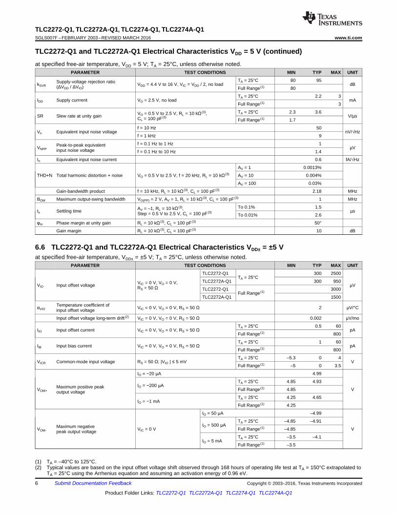
6.1 Absolute Maximum Ratingsover operating free-air temperature range (unless otherwise noted) (1)
MIN MAX UNITSupply voltage, VDD+ (2) 8 VVDD–(2) –8 VDifferential input voltage, VID
(3) ±16 VInput voltage, VI(any input)(2) VDD− − 0.3 VDD+ VInput current, II (any input) ±5 mAOutput current, IO ±50 mATotal current into VDD+ ±50 mATotal current out of VDD– ±50 mADuration of short-circuit current at (or below) 25°C (4) UnlimitedOperating free-air temperature range, TA –40 125 °CLead temperature 1,6 mm (1/16 inch) from case for 10 seconds D or PW package 260 °CStorage temperature, Tstg –65 150 °C
(1) AEC Q100-002 indicates that HBM stressing shall be in accordance with the ANSI/ESDA/JEDEC JS-001 specification.
6.2 ESD RatingsVALUE UNIT
V(ESD) Electrostatic dischargeHuman-body model (HBM), per AEC Q100-002 (1) ±2000
VCharged-device model (CDM), per AEC Q100-011 ±1000
6.3 Recommended Operating Conditionsover operating free-air temperature range (unless otherwise noted)
MIN MAX UNITVDD± Supply voltage ±2.2 ±8 VVI Input voltage VDD− VDD+ −1.5 VVIC Common-mode input voltage VDD− VDD+ −1.5 VTA Operating free-air temperature −40 125 °C

5
TLC2272-Q1, TLC2272A-Q1, TLC2274-Q1, TLC2274A-Q1www.ti.com SGLS007F –FEBRUARY 2003–REVISED MARCH 2016
Product Folder Links: TLC2272-Q1 TLC2272A-Q1 TLC2274-Q1 TLC2274A-Q1
Submit Documentation FeedbackCopyright © 2003–2016, Texas Instruments Incorporated
(1) For more information about traditional and new thermal metrics, see the Semiconductor and IC Package Thermal Metrics applicationreport, SPRA953.
6.4 Thermal Information
THERMAL METRIC (1)TLC2272-Q1 TLC2274-Q1
UNITD (SOIC) PW (TSSOP) D (SOIC) PW (TSSOP)8 PINS 8 PINS 14 PINS 14 PINS
RθJA Junction-to-ambient thermal resistance 115.6 175.8 83.8 111.6 °C/WRθJC(top) Junction-to-case (top) thermal resistance 61.8 58.8 43.2 41.2 °C/WRθJB Junction-to-board thermal resistance 55.9 104.3 38.4 54.7 °C/WψJT Junction-to-top characterization parameter 14.3 5.9 9.4 3.9 °C/W
ψJBJunction-to-board characterizationparameter 55.4 102.3 38.1 53.9 °C/W
RθJC(bot)Junction-to-case (bottom) thermalresistance — — — — °C/W
(1) TA = –40°C to 125°C.(2) Typical values are based on the input offset voltage shift observed through 168 hours of operating life test at TA = 150°C extrapolated to
TA = 25°C using the Arrhenius equation and assuming an activation energy of 0.96 eV.(3) Referenced to 0 V.
6.5 TLC2272-Q1 and TLC2272A-Q1 Electrical Characteristics VDD = 5 Vat specified free-air temperature, VDD = 5 V; TA = 25°C, unless otherwise noted.
PARAMETER TEST CONDITIONS MIN TYP MAX UNIT
VIO Input offset voltage VIC = 0 V, VDD± = ±2.5 V,VO = 0 V, RS = 50 Ω
TLC2272-Q1TA = 25°C
300 2500
µVTLC2272A-Q1 300 950
TLC2272-Q1Full Range (1) 3000
TLC2272A-Q1 1500
αVIOTemperature coefficient ofinput offset voltage VIC = 0 V, VDD± = ±2.5 V, VO = 0 V, RS = 50 Ω 2 μV/°C
Input offset voltage long-term drift (2) VIC = 0 V, VDD± = ±2.5 V, VO = 0 V, RS = 50 Ω 0.002 μV/mo
IIO Input offset current VIC = 0 V, VDD± = ±2.5 V, VO = 0 V, RS = 50 ΩTA = 25°C 0.5 60
pAFull Range (1) 800
IIB Input bias current VIC = 0 V, VDD± = ±2.5 V, VO = 0 V, RS = 50 ΩTA = 25°C 1 60
pAFull Range (1) 800
VICR Common-mode input voltage RS = 50 Ω; |VIO | ≤ 5 mVTA = 25°C –0.3 2.5 4
VFull Range (1) 0 2.5 3.5
VOH High-level output voltage
IOH = −20 μA 4.99
VIOH = −200 μA
TA = 25°C 4.85 4.93
Full Range (1) 4.85
IOH = −1 mATA = 25°C 4.25 4.65
Full Range (1) 4.25
VOL Low-level output voltage VIC = 2.5 V
IOL = 50 μA 0.01
VIOL = 500 μA
TA = 25°C 0.09 0.15
Full Range (1) 0.15
IOL = 5 mATA = 25°C 0.9 1.5
Full Range (1) 1.5
AVDLarge-signal differentialvoltage amplification VIC = 2.5 V, VO = 1 V to 4 V
RL = 10 kΩ (3) TA = 25°C 10 35
V/mVFull Range (1) 10
RL = 1 MΩ (3) 175
rid Differential input resistance 1012 Ω
ri Common-mode input resistance 1012 Ω
ci Common-mode input capacitance f = 10 kHz, P package 8 pF
zo Closed-loop output impedance f = 1 MHz, AV = 10 140 Ω
CMRR Common-mode rejection ratio VIC = 0 V to 2.7 V, VO = 2.5 V, RS = 50 ΩTA = 25°C 70 75
dBFull Range (1) 70
6
TLC2272-Q1, TLC2272A-Q1, TLC2274-Q1, TLC2274A-Q1SGLS007F –FEBRUARY 2003–REVISED MARCH 2016 www.ti.com
Product Folder Links: TLC2272-Q1 TLC2272A-Q1 TLC2274-Q1 TLC2274A-Q1
Submit Documentation Feedback Copyright © 2003–2016, Texas Instruments Incorporated
TLC2272-Q1 and TLC2272A-Q1 Electrical Characteristics VDD = 5 V (continued)at specified free-air temperature, VDD = 5 V; TA = 25°C, unless otherwise noted.
PARAMETER TEST CONDITIONS MIN TYP MAX UNIT
kSVRSupply-voltage rejection ratio(ΔVDD / ΔVIO) VDD = 4.4 V to 16 V, VIC = VDD / 2, no load
TA = 25°C 80 95dB
Full Range (1) 80
IDD Supply currrent VO = 2.5 V, no loadTA = 25°C 2.2 3
mAFull Range (1) 3
SR Slew rate at unity gain VO = 0.5 V to 2.5 V, RL = 10 kΩ (3),CL = 100 pF (3)
TA = 25°C 2.3 3.6V/µs
Full Range (1) 1.7
Vn Equivalent input noise voltagef = 10 Hz 50
nV/√Hzf = 1 kHz 9
VNPPPeak-to-peak equivalentinput noise voltage
f = 0.1 Hz to 1 Hz 1µV
f = 0.1 Hz to 10 Hz 1.4
In Equivalent input noise current 0.6 fA/√Hz
THD+N Total harmonic distortion + noise VO = 0.5 V to 2.5 V, f = 20 kHz, RL = 10 kΩ (3)
AV = 1 0.0013%
AV = 10 0.004%
AV = 100 0.03%
Gain-bandwidth product f = 10 kHz, RL = 10 kΩ (3), CL = 100 pF (3) 2.18 MHz
BOM Maximum output-swing bandwidth VO(PP) = 2 V, AV = 1, RL = 10 kΩ (3), CL = 100 pF (3) 1 MHz
ts Settling time AV = –1, RL = 10 kΩ (3),Step = 0.5 V to 2.5 V, CL = 100 pF (3)
To 0.1% 1.5µs
To 0.01% 2.6
φm Phase margin at unity gain RL = 10 kΩ (3), CL = 100 pF (3) 50°
Gain margin RL = 10 kΩ (3), CL = 100 pF (3) 10 dB
(1) TA = –40°C to 125°C.(2) Typical values are based on the input offset voltage shift observed through 168 hours of operating life test at TA = 150°C extrapolated to
TA = 25°C using the Arrhenius equation and assuming an activation energy of 0.96 eV.
6.6 TLC2272-Q1 and TLC2272A-Q1 Electrical Characteristics VDD± = ±5 Vat specified free-air temperature, VDD± = ±5 V; TA = 25°C, unless otherwise noted.
PARAMETER TEST CONDITIONS MIN TYP MAX UNIT
VIO Input offset voltage VIC = 0 V, VO = 0 V,RS = 50 Ω
TLC2272-Q1TA = 25°C
300 2500
µVTLC2272A-Q1 300 950
TLC2272-Q1Full Range (1) 3000
TLC2272A-Q1 1500
αVIOTemperature coefficient ofinput offset voltage VIC = 0 V, VO = 0 V, RS = 50 Ω 2 μV/°C
Input offset voltage long-term drift (2) VIC = 0 V, VO = 0 V, RS = 50 Ω 0.002 μV/mo
IIO Input offset current VIC = 0 V, VO = 0 V, RS = 50 ΩTA = 25°C 0.5 60
pAFull Range (1) 800
IIB Input bias current VIC = 0 V, VO = 0 V, RS = 50 ΩTA = 25°C 1 60
pAFull Range (1) 800
VICR Common-mode input voltage RS = 50 Ω; |VIO | ≤ 5 mVTA = 25°C –5.3 0 4
VFull Range (1) –5 0 3.5
VOM+Maximum positive peakoutput voltage
IO = −20 μA 4.99
VIO = −200 μA
TA = 25°C 4.85 4.93
Full Range (1) 4.85
IO = −1 mATA = 25°C 4.25 4.65
Full Range (1) 4.25
VOM-Maximum negativepeak output voltage VIC = 0 V
IO = 50 μA –4.99
VIO = 500 μA
TA = 25°C –4.85 –4.91
Full Range (1) –4.85
IO = 5 mATA = 25°C –3.5 –4.1
Full Range (1) –3.5

7
TLC2272-Q1, TLC2272A-Q1, TLC2274-Q1, TLC2274A-Q1www.ti.com SGLS007F –FEBRUARY 2003–REVISED MARCH 2016
Product Folder Links: TLC2272-Q1 TLC2272A-Q1 TLC2274-Q1 TLC2274A-Q1
Submit Documentation FeedbackCopyright © 2003–2016, Texas Instruments Incorporated
TLC2272-Q1 and TLC2272A-Q1 Electrical Characteristics VDD± = ±5 V (continued)at specified free-air temperature, VDD± = ±5 V; TA = 25°C, unless otherwise noted.
PARAMETER TEST CONDITIONS MIN TYP MAX UNIT
AVDLarge-signal differentialvoltage amplification VO = ±4 V
RL = 10 kΩTA = 25°C 20 50
V/mVFull Range (1) 20
RL = 1 MΩ 300
rid Differential input resistance 1012 Ω
ri Common-mode input resistance 1012 Ω
ci Common-mode input capacitance f = 10 kHz, P package 8 pF
zo Closed-loop output impedance f = 1 MHz, AV = 10 130 Ω
CMRR Common-mode rejection ratio VIC = –5 V to 2.7 V, VO = 0 V, RS = 50 ΩTA = 25°C 75 80
dBFull Range (1) 75
kSVRSupply-voltage rejection ratio(ΔVDD / ΔVIO) VDD+ = 2.2 V to ±8 V, VIC = 0 V, no load
TA = 25°C 80 95dB
Full Range (1) 80
IDD Supply currrent VO = 0 V, no loadTA = 25°C 2.4 3
mAFull Range (1) 3
SR Slew rate at unity gain VO = ±2.3 V, RL = 10 kΩ, CL = 100 pFTA = 25°C 2.3 3.6
V/µsFull Range (1) 1.7
Vn Equivalent input noise voltagef = 10 Hz 50
nV/√Hzf = 1 kHz 9
VNPPPeak-to-peak equivalentinput noise voltage
f = 0.1 Hz to 1 Hz 1µV
f = 0.1 Hz to 10 Hz 1.4
In Equivalent input noise current 0.6 fA/√Hz
THD+N Total harmonic distortion + noise VO = ±2.3, f = 20 kHz, RL = 10 kΩ
AV = 1 0.0011%
AV = 10 0.004%
AV = 100 0.03%
Gain-bandwidth product f = 10 kHz, RL = 10 kΩ, CL = 100 pF 2.25 MHz
BOM Maximum output-swing bandwidth VO(PP) = 4.6 V, AV = 1, RL = 10 kΩ, CL = 100 pF 0.54 MHz
ts Settling time AV = –1, RL = 10 kΩ,Step = –2.3 V to 2.3 V, CL = 100 pF
To 0.1% 1.5µs
To 0.01% 3.2
φm Phase margin at unity gain RL = 10 kΩ, CL = 100 pF 52°
Gain margin RL = 10 kΩ, CL = 100 pF 10 dB
8
TLC2272-Q1, TLC2272A-Q1, TLC2274-Q1, TLC2274A-Q1SGLS007F –FEBRUARY 2003–REVISED MARCH 2016 www.ti.com
Product Folder Links: TLC2272-Q1 TLC2272A-Q1 TLC2274-Q1 TLC2274A-Q1
Submit Documentation Feedback Copyright © 2003–2016, Texas Instruments Incorporated
(1) TA = –40°C to 125°C.(2) Typical values are based on the input offset voltage shift observed through 168 hours of operating life test at TA = 150°C extrapolated to
TA = 25°C using the Arrhenius equation and assuming an activation energy of 0.96 eV.(3) Referenced to 0 V.
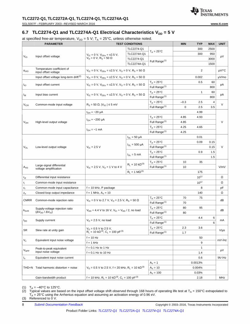
6.7 TLC2274-Q1 and TLC2274A-Q1 Electrical Characteristics VDD = 5 Vat specified free-air temperature, VDD = 5 V; TA = 25°C, unless otherwise noted.
PARAMETER TEST CONDITIONS MIN TYP MAX UNIT
VIO Input offset voltage VIC = 0 V, VDD± = ±2.5 V,VO = 0 V, RS = 50 Ω
TLC2274-Q1TA = 25°C
300 2500
µVTLC2274A-Q1 300 950
TLC2274-Q1Full Range (1) 3000
TLC2274A-Q1 1500
αVIOTemperature coefficient ofinput offset voltage VIC = 0 V, VDD± = ±2.5 V, VO = 0 V, RS = 50 Ω 2 μV/°C
Input offset voltage long-term drift (2) VIC = 0 V, VDD± = ±2.5 V, VO = 0 V, RS = 50 Ω 0.002 μV/mo
IIO Input offset current VIC = 0 V, VDD± = ±2.5 V, VO = 0 V, RS = 50 ΩTA = 25°C 0.5 60
pAFull Range (1) 800
IIB Input bias current VIC = 0 V, VDD± = ±2.5 V, VO = 0 V, RS = 50 ΩTA = 25°C 1 60
pAFull Range (1) 800
VICR Common-mode input voltage RS = 50 Ω; |VIO | ≤ 5 mVTA = 25°C –0.3 2.5 4
VFull Range (1) 0 2.5 3.5
VOH High-level output voltage
IOH = −20 μA 4.99
VIOH = −200 μA
TA = 25°C 4.85 4.93
Full Range (1) 4.85
IOH = −1 mATA = 25°C 4.25 4.65
Full Range (1) 4.25
VOL Low-level output voltage VIC = 2.5 V
IOL = 50 μA 0.01
VIOL = 500 μA
TA = 25°C 0.09 0.15
Full Range (1) 0.15
IOL = 5 mATA = 25°C 0.9 1.5
Full Range (1) 1.5
AVDLarge-signal differentialvoltage amplification VIC = 2.5 V, VO = 1 V to 4 V
RL = 10 kΩ (3) TA = 25°C 10 35
V/mVFull Range (1) 10
RL = 1 MΩ (3) 175
rid Differential input resistance 1012 Ω
ri Common-mode input resistance 1012 Ω
ci Common-mode input capacitance f = 10 kHz, P package 8 pF
zo Closed-loop output impedance f = 1 MHz, AV = 10 140 Ω
CMRR Common-mode rejection ratio VIC = 0 V to 2.7 V, VO = 2.5 V, RS = 50 ΩTA = 25°C 70 75
dBFull Range (1) 70
kSVRSupply-voltage rejection ratio(ΔVDD / ΔVIO) VDD = 4.4 V to 16 V, VIC = VDD / 2, no load
TA = 25°C 80 95dB
Full Range (1) 80
IDD Supply currrent VO = 2.5 V, no loadTA = 25°C 4.4 6
mAFull Range (1) 6
SR Slew rate at unity gain VO = 0.5 V to 2.5 V,RL = 10 kΩ (3), CL = 100 pF (3)
TA = 25°C 2.3 3.6V/µs
Full Range (1) 1.7
Vn Equivalent input noise voltagef = 10 Hz 50
nV/√Hzf = 1 kHz 9
VNPPPeak-to-peak equivalentinput noise voltage
f = 0.1 Hz to 1 Hz 1µV
f = 0.1 Hz to 10 Hz 1.4
In Equivalent input noise current 0.6 fA/√Hz
THD+N Total harmonic distortion + noise VO = 0.5 V to 2.5 V, f = 20 kHz, RL = 10 kΩ (3)
AV = 1 0.0013%
AV = 10 0.004%
AV = 100 0.03%
Gain-bandwidth product f = 10 kHz, RL = 10 kΩ (3), CL = 100 pF (3) 2.18 MHz
9
TLC2272-Q1, TLC2272A-Q1, TLC2274-Q1, TLC2274A-Q1www.ti.com SGLS007F –FEBRUARY 2003–REVISED MARCH 2016
Product Folder Links: TLC2272-Q1 TLC2272A-Q1 TLC2274-Q1 TLC2274A-Q1
Submit Documentation FeedbackCopyright © 2003–2016, Texas Instruments Incorporated
TLC2274-Q1 and TLC2274A-Q1 Electrical Characteristics VDD = 5 V (continued)at specified free-air temperature, VDD = 5 V; TA = 25°C, unless otherwise noted.
PARAMETER TEST CONDITIONS MIN TYP MAX UNIT
BOM Maximum output-swing bandwidth VO(PP) = 2 V, AV = 1, RL = 10 kΩ (3), CL = 100 pF (3) 1 MHz
ts Settling time AV = –1, RL = 10 kΩ (3),Step = 0.5 V to 2.5 V, CL = 100 pF (3)
To 0.1% 1.5µs
To 0.01% 2.6
φm Phase margin at unity gain RL = 10 kΩ (3), CL = 100 pF (3) 50°
Gain margin RL = 10 kΩ (3), CL = 100 pF (3) 10 dB
(1) TA = –40°C to 125°C.(2) Typical values are based on the input offset voltage shift observed through 168 hours of operating life test at TA = 150°C extrapolated to
TA = 25°C using the Arrhenius equation and assuming an activation energy of 0.96 eV.
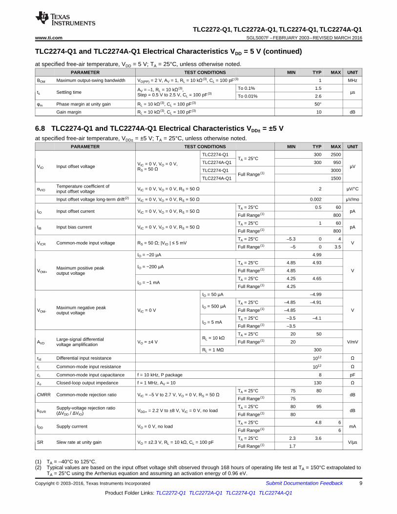
6.8 TLC2274-Q1 and TLC2274A-Q1 Electrical Characteristics VDD± = ±5 Vat specified free-air temperature, VDD± = ±5 V; TA = 25°C, unless otherwise noted.
PARAMETER TEST CONDITIONS MIN TYP MAX UNIT
VIO Input offset voltage VIC = 0 V, VO = 0 V,RS = 50 Ω
TLC2274-Q1TA = 25°C
300 2500
µVTLC2274A-Q1 300 950
TLC2274-Q1Full Range (1) 3000
TLC2274A-Q1 1500
αVIOTemperature coefficient ofinput offset voltage VIC = 0 V, VO = 0 V, RS = 50 Ω 2 μV/°C
Input offset voltage long-term drift (2) VIC = 0 V, VO = 0 V, RS = 50 Ω 0.002 μV/mo
IIO Input offset current VIC = 0 V, VO = 0 V, RS = 50 ΩTA = 25°C 0.5 60
pAFull Range (1) 800
IIB Input bias current VIC = 0 V, VO = 0 V, RS = 50 ΩTA = 25°C 1 60
pAFull Range (1) 800
VICR Common-mode input voltage RS = 50 Ω; |VIO | ≤ 5 mVTA = 25°C –5.3 0 4
VFull Range (1) –5 0 3.5
VOM+Maximum positive peakoutput voltage
IO = −20 μA 4.99
VIO = −200 μA
TA = 25°C 4.85 4.93
Full Range (1) 4.85
IO = −1 mATA = 25°C 4.25 4.65
Full Range (1) 4.25
VOM-Maximum negative peakoutput voltage VIC = 0 V
IO = 50 μA –4.99
VIO = 500 μA
TA = 25°C –4.85 –4.91
Full Range (1) –4.85
IO = 5 mATA = 25°C –3.5 –4.1
Full Range (1) –3.5
AVDLarge-signal differentialvoltage amplification VO = ±4 V
RL = 10 kΩTA = 25°C 20 50
V/mVFull Range (1) 20
RL = 1 MΩ 300
rid Differential input resistance 1012 Ω
ri Common-mode input resistance 1012 Ω
ci Common-mode input capacitance f = 10 kHz, P package 8 pF
zo Closed-loop output impedance f = 1 MHz, AV = 10 130 Ω
CMRR Common-mode rejection ratio VIC = –5 V to 2.7 V, VO = 0 V, RS = 50 ΩTA = 25°C 75 80
dBFull Range (1) 75
kSVRSupply-voltage rejection ratio(ΔVDD / ΔVIO) VDD+ = 2.2 V to ±8 V, VIC = 0 V, no load
TA = 25°C 80 95dB
Full Range (1) 80
IDD Supply currrent VO = 0 V, no loadTA = 25°C 4.8 6
mAFull Range (1) 6
SR Slew rate at unity gain VO = ±2.3 V, RL = 10 kΩ, CL = 100 pFTA = 25°C 2.3 3.6
V/µsFull Range (1) 1.7

10
TLC2272-Q1, TLC2272A-Q1, TLC2274-Q1, TLC2274A-Q1SGLS007F –FEBRUARY 2003–REVISED MARCH 2016 www.ti.com
Product Folder Links: TLC2272-Q1 TLC2272A-Q1 TLC2274-Q1 TLC2274A-Q1
Submit Documentation Feedback Copyright © 2003–2016, Texas Instruments Incorporated
TLC2274-Q1 and TLC2274A-Q1 Electrical Characteristics VDD± = ±5 V (continued)at specified free-air temperature, VDD± = ±5 V; TA = 25°C, unless otherwise noted.
PARAMETER TEST CONDITIONS MIN TYP MAX UNIT
Vn Equivalent input noise voltagef = 10 Hz 50
nV/√Hzf = 1 kHz 9
VNPPPeak-to-peak equivalentinput noise voltage
f = 0.1 Hz to 1 Hz 1µV
f = 0.1 Hz to 10 Hz 1.4
In Equivalent input noise current 0.6 fA/√Hz
THD+N Total harmonic distortion + noise VO = ±2.3, f = 20 kHz, RL = 10 kΩ
AV = 1 0.0011%
AV = 10 0.004%
AV = 100 0.03%
Gain-bandwidth product f = 10 kHz, RL = 10 kΩ, CL = 100 pF 2.25 MHz
BOM Maximum output-swing bandwidth VO(PP) = 4.6 V, AV = 1, RL = 10 kΩ, CL = 100 pF 0.54 MHz
ts Settling time AV = –1, RL = 10 kΩ,Step = –2.3 V to 2.3 V, CL = 100 pF
To 0.1% 1.5µs
To 0.01% 3.2
φm Phase margin at unity gain RL = 10 kΩ, CL = 100 pF 52°
Gain margin RL = 10 kΩ, CL = 100 pF 10 dB

11
TLC2272-Q1, TLC2272A-Q1, TLC2274-Q1, TLC2274A-Q1www.ti.com SGLS007F –FEBRUARY 2003–REVISED MARCH 2016
Product Folder Links: TLC2272-Q1 TLC2272A-Q1 TLC2274-Q1 TLC2274A-Q1
Submit Documentation FeedbackCopyright © 2003–2016, Texas Instruments Incorporated
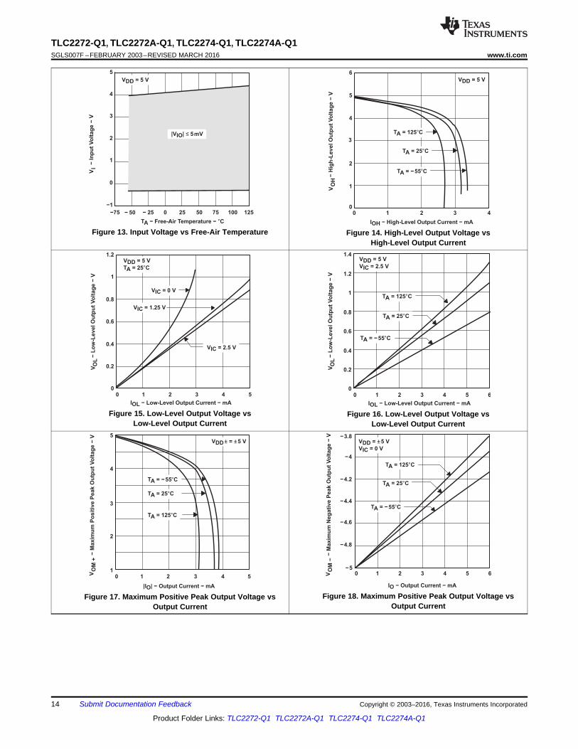
(1) For all graphs where VDD = 5 V, all loads are referenced to 2.5 V.(2) Data at high and low temperatures are applicable only within the rated operating free-air temperature ranges of the various devices.
6.9 Typical CharacteristicsTable 1. Table of Graphs
FIGURE (1)
VIO Input offset voltageDistribution 1, 2, 3, 4vs Common-mode voltage 5, 6
αVIO Input offset voltage temperature coefficient Distribution 7, 8, 9, 10 (2)
IIB /IIO Input bias and input offset current vs Free-air temperature 11 (2)
VI Input voltagevs Supply voltage 12vs Free-air temperature 13 (2)
VOH High-level output voltage vs High-level output current 14 (2)
VOL Low-level output voltage vs Low-level output current 15, 16 (2)
VOM+ Maximum positive peak output voltage vs Output current 17 (2)
VOM- Maximum negative peak output voltage vs Output current 18 (2)
VO(PP) Maximum peak-to-peak output voltage vs Frequency 19
IOS Short-circuit output currentvs Supply voltage 20vs Free-air temperature 21 (2)
VO Output voltage vs Differential input voltage 22, 23
AVD
Large-signal differential voltage amplification vs Load resistance 24Large-signal differential voltage amplification and phase margin vs Frequency 25, 26Large-signal differential voltage amplification vs Free-air temperature 27 (2), 28 (2)
z0 Output impedance vs Frequency 29, 30
CMRR Common-mode rejection ratiovs Frequency 31vs Free-air temperature 32
kSVR Supply-voltage rejection ratiovs Frequency 33, 34vs Free-air temperature 35 (2)
IDD Supply currentvs Supply voltage 36 (2), 37 (2)
vs Free-air temperature 38 (2), 39 (2)
SR Slew ratevs Load Capacitance 40vs Free-air temperature 41 (2)
VO
Inverting large-signal pulse response 42, 43Voltage-follower large-signal pulse response 44, 45Inverting small-signal pulse response 46, 47Voltage-follower small-signal pulse response 48, 49
Vn Equivalent input noise voltage vs Frequency 50, 51Noise voltage over a 10-second period 52Integrated noise voltage vs Frequency 53
THD+N Total harmonic distortion + noise vs Frequency 54
Gain-bandwidth productvs Supply voltage 55vs Free-air temperature 56 (2)
φm Phase margin vs Load capacitance 57Gain margin vs Load capacitance 58

0.5
0
−1−1 0 1
VIO
−In
pu
tO
ffset
Vo
ltag
e−
mV
1
2 3 4 5
VIO
VIC − Common-Mode Voltage − V
VDD = 5 V
TA = 25°C
RS = 50 Ω
−0.5
0.5
0
−1−1 0 1
VIO
−In
pu
tO
ffset
Vo
ltag
e−
mV
1
2 3 4 5
VIC − Common-Mode Voltage − V
VIO
−0.5
VDD = ±5 V
TA = 25°C
RS = 50 Ω
−6 −5 −4 −3 −2
VIO − Input Offset Voltage − mV
Perc
en
tag
eo
fA
mp
lifi
ers
−%
10
5
0
20
15
0 0.4 0.8 1.2 1.6
992 Amplifiers From
−1.6 −1.2 −0.8 −0.4
2 Wafer Lots
VDD = ±2.5 V
VIO − Input Offset Voltage − mV
Perc
en
tag
eo
fA
mp
lifi
ers
−%
10
5
0
20
15
0 0.4 0.8 1.2 1.6
992 Amplifiers From
−1.6 −1.2 −0.8 −0.4
2 Wafer Lots
VDD = ±5 V
VIO − Input Offset Voltage − mV
Perc
en
tag
eo
fA
mp
lifi
ers
−%
10
5
0
20
15
−1.6 −1.2 0 0.4 0.8 1.2 1.6
891 Amplifiers From
−0.8 −0.4
2 Wafer Lots
VDD = ±2.5 V
TA = 25°C
VIO − Input Offset Voltage − mV
Perc
en
tag
eo
fA
mp
lifi
ers
−%
10
5
0
20
15
−1.6 −1.2 0 0.4 0.8 1.2 1.6−0.8 −0.4
891 Amplifiers From
2 Wafer Lots
VDD = ±5 V
TA = 25°C
12
TLC2272-Q1, TLC2272A-Q1, TLC2274-Q1, TLC2274A-Q1SGLS007F –FEBRUARY 2003–REVISED MARCH 2016 www.ti.com
Product Folder Links: TLC2272-Q1 TLC2272A-Q1 TLC2274-Q1 TLC2274A-Q1
Submit Documentation Feedback Copyright © 2003–2016, Texas Instruments Incorporated
Figure 1. Distribution of TLC2272-Q1 Input Offset Voltage Figure 2. Distribution of TLC2272-Q1 Input Offset Voltage
Figure 3. Distribution of TLC2274-Q1 Input Offset Voltage Figure 4. Distribution of TLC2274-Q1 Input Offset Voltage
Figure 5. Input Offset Voltage vs Common-Mode Voltage Figure 6. Input Offset Voltage vs Common-Mode Voltage

15
10
5
0
25 45 65 85
20
25
30
105 125
TA − Free-Air Temperature − °C
35
VDD = ±2.5 V
VIC = 0 V
VO = 0 V
RS = 50 Ω
IIB
IIO
IIB
an
dIIO
−In
pu
tB
ias
an
dIn
pu
tO
ffset
Cu
rren
ts−
pA
IBII I
O
0
− 2
− 6
− 8
− 10
8
− 4
2 3 4 5 6 7 8
−In
pu
t V
olt
ag
e−
V
4
2
6
10
|VDD±| − Supply Voltage − V
VI
TA = 25°C
RS = 50 Ω
|VIO| ≤ 5mV
12
15
10
5
00 1
Perc
en
tag
eo
fA
mp
lifi
ers
−%
20
25
2 3 4 5
αVIO − Temperature Coefficient − µ °V/ C
−5 −4 −3 −2 −1
128 Amplifiers From
2 Wafer Lots
VDD = ±2.5 V
N Package
TA = 25°C to 125°C
15
10
5
0
Perc
en
tag
eo
fA
mp
lifi
ers
−%
20
25
αVIO − Temperature Coefficient − µ °V/ C
0 1 2 3 4 5−5 −4 −3 −2 −1
128 Amplifiers From
2 Wafer Lots
VDD = ±2.5 V
N Package
TA = 25°C to 125°C
15
10
5
0−1 0 1
Perc
en
tag
eo
fA
mp
lifi
ers
−%
20
25
2 3 4 5
αVIO − Temperature Coefficient − µ °V/ C
128 Amplifiers From
2 Wafer Lots
VDD = ±2.5 V
P Package
25°C to 125°C
−5 −4 −3 −2 −5 −4 −3 −2
15
10
5
0−1 0 1
Perc
en
tag
eo
fA
mp
lifi
ers
−%
20
25
2 3 4 5
αVIO − Temperature Coefficient − µ °V/ C
128 Amplifiers From
2 Wafer Lots
VDD = ±5 V
P Package
25°C to 125°C
13
TLC2272-Q1, TLC2272A-Q1, TLC2274-Q1, TLC2274A-Q1www.ti.com SGLS007F –FEBRUARY 2003–REVISED MARCH 2016
Product Folder Links: TLC2272-Q1 TLC2272A-Q1 TLC2274-Q1 TLC2274A-Q1
Submit Documentation FeedbackCopyright © 2003–2016, Texas Instruments Incorporated
Figure 7. Distribution of TLC2272-Q1 vsInput Offset Voltage Temperature Coefficient
Figure 8. Distribution of TLC2272-Q1 vsInput Offset Voltage Temperature Coefficient
Figure 9. Distribution of TLC2274-Q1 vsInput Offset Voltage Temperature Coefficient
Figure 10. Distribution of TLC2274-Q1 vsInput Offset Voltage Temperature Coefficient
Figure 11. Input Bias and Input Offset Current vsFree-Air Temperature
Figure 12. Input Voltage vs Supply Voltage
3
2
10 1 2 3 4 5
−M
axim
um
Po
sit
ive
Peak
Ou
tpu
tV
olt
ag
e−
V
4
5
|IO| − Output Current − mA
TA = −55°C
TA = 25°C
TA = 125°C
VDD± = ±5 V
VO
M +
0 1 2 3 4 5 6
IO − Output Current − mA
VDD = ±5 V
VIC = 0 V
TA = 125°C
TA = 25°C
TA = −55°C
−3.8
−4
−4.2
−4.4
−4.6
−4.8
−5
−M
axim
um
Neg
ati
ve
Peak
Ou
tpu
tV
olt
ag
e−
VV
OM
−V
OL
−L
ow
-LevelO
utp
ut
Vo
ltag
e−
V
IOL − Low-Level Output Current − mA
VO
L0.6
0.4
0.2
00 1 2 3
0.8
4
1
1.2
5 6
1.4VDD = 5 V
VIC = 2.5 V
TA = 125°C
TA = 25°C
TA = −55°C
VO
L−
Lo
w-L
evelO
utp
ut
Vo
ltag
e−
V
0.6
0.4
0.2
00 1 2 3
0.8
4 5
VDD = 5 V
TA = 25°C
IOL − Low-Level Output Current − mA
VO
L
VIC = 1.25 V
1
1.2
VIC = 2.5 V
VIC = 0 V
V0H
−H
igh
-LevelO
utp
ut
Vo
ltag
e−
VV
OH
IOH − High-Level Output Current − mA
4
2
1
0
6
3
0 1 2 3 4
5
VDD = 5 V
TA = 125°C
TA = −55°C
TA = 25°C
−75 − 25 0 25 50 75 100 125
2
1
0
−1
3
4
5
−In
pu
t V
olt
ag
e−
VV
I
TA − Free-Air Temperature − °C
|VIO| ≤ 5mV
VDD = 5 V
− 50
14
TLC2272-Q1, TLC2272A-Q1, TLC2274-Q1, TLC2274A-Q1SGLS007F –FEBRUARY 2003–REVISED MARCH 2016 www.ti.com
Product Folder Links: TLC2272-Q1 TLC2272A-Q1 TLC2274-Q1 TLC2274A-Q1
Submit Documentation Feedback Copyright © 2003–2016, Texas Instruments Incorporated
Figure 13. Input Voltage vs Free-Air Temperature Figure 14. High-Level Output Voltage vsHigh-Level Output Current
Figure 15. Low-Level Output Voltage vsLow-Level Output Current
Figure 16. Low-Level Output Voltage vsLow-Level Output Current
Figure 17. Maximum Positive Peak Output Voltage vsOutput Current
Figure 18. Maximum Positive Peak Output Voltage vsOutput Current

1
−1
−3
−50 250
3
5
500 750 1000
VID − Differential Input Voltage − µV
−O
utp
ut
Vo
ltag
e−
VV
O
−1000 −750 −250−500
VDD = ±5 V
TA = 25°C
RL = 10 kΩ
VIC = 0 V
0.1
1
0.1 1 10 100
10
100
1000
RL − Load Resistance − kΩ
VO = ±1 V
TA = 25°C
VDD = ±5 V
VDD = 5 V
AV
D−
Larg
e-S
ign
al
Dif
fere
nti
al
AV
D Vo
ltag
eA
mp
lifi
cati
on
−d
B
−5
−75 −50 −25 0 25 50 75 100 125
−1
−3
7
11
15
IOS
−S
ho
rt-C
ircu
itO
utp
ut
Cu
rren
t−
mA
OS
I
TA − Free-Air Temperature − °C
VID = 100 mV
VID = −100 mV
VO = 0 VVDD = ±5 V
3
2
1
0800
4
5
1200
VID − Differential Input Voltage − µV
−O
utp
ut
Vo
ltag
e−
VV
O
−800 −400 4000
VDD = 5 V
TA = 25°C
RL = 10 kΩ
VIC = 2.5 V
4
0
2 3 4
8
12
16
5 6 7 8
IOS
−S
ho
rt-C
ircu
it O
utp
ut
Cu
rren
t−
mA
OS
I
|VDD±| − Supply Voltage − V
VID = 100 mV
VO = 0 V
TA = 25°C
−8
VID = −100 mV
−4
2
1
0
10 k 100 k 1 M
3
f − Frequency − Hz
4
10 M
6
5
7
8
9
10
V(O
PP
)−
Maxim
um
Peak-t
o-P
eak
Ou
tpu
tV
olt
ag
e−
VV
O(P
P)
VDD = 5 V
VDD = ±5 V
RL = 10 kΩ
TA = 25°C
15
TLC2272-Q1, TLC2272A-Q1, TLC2274-Q1, TLC2274A-Q1www.ti.com SGLS007F –FEBRUARY 2003–REVISED MARCH 2016
Product Folder Links: TLC2272-Q1 TLC2272A-Q1 TLC2274-Q1 TLC2274A-Q1
Submit Documentation FeedbackCopyright © 2003–2016, Texas Instruments Incorporated
Figure 19. Maximum Peak-to-Peak Output Voltage vsFrequency
Figure 20. Short-Circuit Output Current vs Supply Voltage
Figure 21. Short-Circuit Output Current vsFree-Air Temperature
Figure 22. Output Voltage vs Differential Input Voltage
Figure 23. Output Voltage vs Differential Input Voltage Figure 24. Large-Signal Differential Voltage Amplification vsLoad Resistance

10
1
0.1
1000
100
100 1 k 10 k 100 k 1 M
zo
−O
utp
ut
Imp
ed
an
ce
−O
f − Frequency − Hz
Ωzo
VDD = 5 V
TA = 25°C
AV = 100
AV = 10
AV = 1
10
1
0.1
1000
100
100 1 k 10 k 100 k 1 M
zo
−O
utp
ut
Imp
ed
an
ce
−O
f − Frequency − Hz
Ωzo
VDD = ±5 V
TA = 25°C
AV = 100
AV = 10
AV = 1
−75 −50 −25 0 25 50 75 100 125
10
100
1 k
TA − Free-Air Temperature − °C
VDD = 5 V
VIC = 2.5 V
VO = 1 V to 4 V
RL = 1 MΩ
RL = 10 kΩ
AV
D−
Larg
e-S
ign
al D
iffe
ren
tial
AV
DV
olt
ag
eA
mp
lifi
cati
on
−V
/mV
−75 −50 −25 0 25 50 75 100 125
10
100
1 k
TA − Free-Air Temperature − °C
RL = 1 MΩ
RL = 10 kΩ
VDD = ±5 V
VIC = 0 V
VO = ± 4 V
AV
D−
Larg
e-S
ign
al D
iffe
ren
tial
AV
DV
olt
ag
eA
mp
lifi
cati
on
−V
/mV
0
20
1 k 10 k 100 k 1 M
40
60
80
f − Frequency − Hz
10 M
om
−P
hase M
arg
inφ
m
VDD = 5 V
RL = 10 kΩ
CL = 100 pF
TA = 25°C
−20
−40 −90°
−45°
0°
45°
90°
135°
180°A
VD
−L
arg
e-S
ign
al D
iffe
ren
tial
AV
D Vo
ltag
eA
mp
lifi
cati
on
−d
B
0
20
1 k 10 k 100 k 1 M
40
60
80
f − Frequency − Hz
10 M
VDD = ±5 V
RL = 10 kΩ
CL = 100 pF
TA = 25°C
om
−P
hase
Marg
inφ
m
−20
−40 −90°
−45°
0°
45°
90°
135°
180°
AV
D−
Larg
e-S
ign
al
Dif
fere
nti
al
AV
D Vo
ltag
eA
mp
lifi
cati
on
−d
B
16
TLC2272-Q1, TLC2272A-Q1, TLC2274-Q1, TLC2274A-Q1SGLS007F –FEBRUARY 2003–REVISED MARCH 2016 www.ti.com
Product Folder Links: TLC2272-Q1 TLC2272A-Q1 TLC2274-Q1 TLC2274A-Q1
Submit Documentation Feedback Copyright © 2003–2016, Texas Instruments Incorporated
Figure 25. Large-Signal Differential Voltage Amplificationand Phase Margin vs Frequency
Figure 26. Large-Signal Differential Voltage Amplificationand Phase Margin vs Frequency
Figure 27. Large-Signal Differential Voltage Amplification vsFree-Air Temperature
Figure 28. Large-Signal Differential Voltage Amplification vsFree-Air Temperature
Figure 29. Output Impedance vs Frequency Figure 30. Output Impedance vs Frequency

kS
VR
−S
up
ply
Vo
ltag
e R
eje
cti
on
Rati
o−
dB
kS
VR
TA − Free-Air Temperature − °C
−75 −50 −25 0 25 50 75 100 125
100
95
90
85
105
110VDD± = ±2.2 V to ±8 V
VO = 0 V
0 1 2 3 4 5 6 7 8
0
0.6
1.2
1.8
2.4
3
IDD
−S
up
ply
Cu
rren
t−
mA
DD
I
|VDD± | − Supply Voltage − V
VO = 0 V
No Load
TA = 25°C
TA = −55°C
TA = 125°C
40
20
0
10 100 1 k
kS
VR
−S
up
ply
-Vo
ltag
eR
eje
cti
on
Rati
o−
dB
60
80
f − Frequency − Hz
100
10 k 100 k 1 M 10 M
kS
VR
VDD = 5 V
TA = 25°C
kSVR+
kSVR−
−20
40
20
0
10 100 1 k
kS
VR
−S
up
ply
-Vo
ltag
eR
eje
cti
on
Rati
o−
dB
60
80
f − Frequency − Hz
100
10 k 100 k 1 M 10 M
kS
VR
VDD = ±5 V
TA = 25°C
kSVR+
kSVR−
−20
60
40
20
010 100 1 k 10 k
CM
RR
−C
om
mo
n-M
od
e R
eje
cti
on
Rati
o−
dB
80
100
100 k 1 M
f − Frequency − Hz
VDD = ±5 V
VDD = 5 V
10 M
TA = 25°C
TA − Free-Air Temperature − °C
CM
RR
−C
om
mo
n-M
od
e R
eje
cti
on
Rati
o−
dB
82
78
74
70
86
90
−75 −50 −25 0 25 50 75 100 125
VDD = ±5 V
VDD = 5 V
VIC = 0 V to 2.7 V
VIC = −5 V to 2.7 V
17
TLC2272-Q1, TLC2272A-Q1, TLC2274-Q1, TLC2274A-Q1www.ti.com SGLS007F –FEBRUARY 2003–REVISED MARCH 2016
Product Folder Links: TLC2272-Q1 TLC2272A-Q1 TLC2274-Q1 TLC2274A-Q1
Submit Documentation FeedbackCopyright © 2003–2016, Texas Instruments Incorporated
Figure 31. Common-Mode Rejection Ratio vs Frequency Figure 32. Common-Mode Rejection Ratio vsFree-Air Temperature
Figure 33. Supply-Voltage Rejection Ratio vs Frequency Figure 34. Supply-Voltage Rejection Ratio vs Frequency
Figure 35. Supply-Voltage Rejection Ratio vsFree-Air Temperature
Figure 36. TLC2272-Q1 Supply Current vs Supply Voltage

3
2
1
4
µs
SR
−S
lew
Rate
−V
/
−75 −50 −25 0 25 50 75 100 125
TA − Free-Air Temperature − °C
VDD = 5 V
RL = 10 kΩ
CL = 100 pF
AV = 1
SR +
SR −
0
5
2
1
01 2 3 4 5
3
4
5
6 7 8 9
VO
−O
utp
ut
Vo
ltag
e−
mV
VO
t − Time − µs
VDD = 5 V
RL = 10 kΩ
CL = 100 pF
TA = 25°C
AV = −1
0
−75 −50 −25 0 25 50 75 100 1250
1.2
2.4
3.6
4.8
6
TA − Free-Air Temperature − °C
IDD
−S
up
ply
Cu
rren
t−
mA
DD
I
VDD = 5 V
VO = 2.5 V
VDD = ±5 V
VO = 0 V
µs
SR
−S
lew
Rate
−V
/
0
1
2
3
CL − Load Capacitance − pF
10 k1 k10010
SR +
SR −
4
5VDD = 5 V
AV = −1
TA = 25°C
−75 −50 −25 0 25 50 75 100 1250
0.6
1.2
1.8
2.4
3
TA − Free-Air Temperature − °C
IDD
−S
up
ply
Cu
rren
t−
mA
DD
I
VDD = 5 V
VO = 2.5 V
VDD = ±5 V
VO = 0 V
0 1 2 3 4 5 6 7 80
1.2
2.4
3.6
4.8
6
IDD
−S
up
ply
Cu
rren
t−
mA
DD
I
|VDD± | − Supply Voltage − V
VO = 0 V
No Load
TA = 25°C
TA = −55°C
TA = 125°C
18
TLC2272-Q1, TLC2272A-Q1, TLC2274-Q1, TLC2274A-Q1SGLS007F –FEBRUARY 2003–REVISED MARCH 2016 www.ti.com
Product Folder Links: TLC2272-Q1 TLC2272A-Q1 TLC2274-Q1 TLC2274A-Q1
Submit Documentation Feedback Copyright © 2003–2016, Texas Instruments Incorporated
Figure 37. TLC2274-Q1 Supply Current vs Supply Voltage Figure 38. TLC2272-Q1 Supply Current vs Free-AirTemperature
Figure 39. TLC2274-Q1 Supply Current vs Free-AirTemperature
Figure 40. Slew Rate vs Load Capacitance
Figure 41. Slew Rate vs Free-Air Temperature Figure 42. Inverting Large-Signal Pulse Response

0
−1000 0.5 1 1.5 2
50
100
2.5 3 3.5 4
VO
−O
utp
ut
Vo
ltag
e−
mV
VO
t − Time − µs
VDD = ±5 V
RL = 10 kΩ
CL = 100 pF
TA = 25°C
AV = 1
−50
2.5
2.45
2.4
2.55
2.6
0 0.5 1 1.5
VO
−O
utp
ut
Vo
ltag
e−
VV
O
t − Time − µs
2.65VDD = 5 V
RL = 10 kΩ
CL = 100 pF
TA = 25°C
AV = 1
0
−1
4
1 2 3 4 5
2
1
3
5
6 7 8 9
VO
−O
utp
ut
Vo
ltag
e−
VV
O
t − Time − µs
VDD = ±5 V
RL = 10 kΩ
CL = 100 pF
TA = 25°C
AV = 1
0
−2
−3
−5
−4
2.5
2.45
2.40.5 1 1.5 2 2.5
2.55
2.6
2.65
3.5 4.5 5 5.5
VO
−O
utp
ut
Vo
ltag
e−
VV
O
t − Time − µs
VDD = 5 V
RL = 10 kΩ
CL = 100 pF
TA = 25°C
AV = −1
0 3 4
3
2
1
01 2 3 4 5
4
5
6 7 8 9
VO
−O
utp
ut
Vo
ltag
e−
VV
O
t − Time − µs
VDD = 5 V
RL = 10 kΩ
CL = 100 pF
AV = 1
TA = 25°C
0
0
− 1
− 3
− 4
− 5
4
− 2
1 2 3 4 5
2
1
3
5
6 7 8 9
VO
−O
utp
ut
Vo
ltag
e−
VV
O
t − Time − µs
VDD = ±5 V
RL = 10 kΩ
CL = 100 pF
TA = 25°C
AV = −1
0
19
TLC2272-Q1, TLC2272A-Q1, TLC2274-Q1, TLC2274A-Q1www.ti.com SGLS007F –FEBRUARY 2003–REVISED MARCH 2016
Product Folder Links: TLC2272-Q1 TLC2272A-Q1 TLC2274-Q1 TLC2274A-Q1
Submit Documentation FeedbackCopyright © 2003–2016, Texas Instruments Incorporated
Figure 43. Inverting Large-Signal Pulse Response Figure 44. Voltage-Follower Large-Signal Pulse Response
Figure 45. Voltage-Follower Large-Signal Pulse Response Figure 46. Inverting Small-Signal Pulse Response
Figure 47. Inverting Small-Signal Pulse Response Figure 48. Voltage-Follower Small-Signal Pulse Response

0.0001
0.001
100 1 k 10 k 100 k
TH
D+
N−
To
talH
arm
on
icD
isto
rtio
nP
lus
No
ise
−%
f − Frequency − Hz
0.01
0.1
1
VDD = 5 V
TA = 25°C
RL = 10 kΩ
AV = 100
AV = 10
AV = 1
Inte
gra
ted
No
ise
Vo
ltag
e−
uV
RM
S
1
0.1
100
1 10 100 1 k
f − Frequency − Hz
10 k 100 k
VR
MS
µ
Calculated UsingIdeal Pass-Band FilterLower Frequency = 1 HzTA= 25°C
10
20
10
010 100 1 k
Vn
−E
qu
ivale
nt
Inp
ut
No
ise V
olt
ag
e−
nV
Hz
30
f − Frequency − Hz
40
10 k
60
Vn
nV
/H
z
VDD = ±5 V
TA = 25°C
RS = 20 Ω
−750
−10002 4 6
0
250
8 10
No
ise V
olt
ag
e−
nV
t − Time − s
0
VDD = 5 V
f = 0.1 Hz to 10 Hz
TA = 25°C
500
750
1000
−250
−500
0
−50
−100
50
100
0 0.5 1 1.5
VO
−O
utp
ut
Vo
ltag
e−
mV
VO
t − Time − µs
VDD = ±5 V
RL = 10 kΩ
CL = 100 pF
TA = 25°C
AV = 1
20
10
010 100 1 k
Vn
−E
qu
ivale
nt
Inp
ut
No
ise
Vo
ltag
e−
nV
Hz
30
f − Frequency − Hz
40
10 k
60
Vn
nV
/H
z
VDD = 5 V
TA = 25°C
RS = 20 Ω
20
TLC2272-Q1, TLC2272A-Q1, TLC2274-Q1, TLC2274A-Q1SGLS007F –FEBRUARY 2003–REVISED MARCH 2016 www.ti.com
Product Folder Links: TLC2272-Q1 TLC2272A-Q1 TLC2274-Q1 TLC2274A-Q1
Submit Documentation Feedback Copyright © 2003–2016, Texas Instruments Incorporated
Figure 49. Voltage-Follower Small-Signal Pulse Response Figure 50. Equivalent Input Noise Voltage vs Frequency
Figure 51. Equivalent Input Noise Voltage vs Frequency Figure 52. Noise Voltage Over a 10 Second Period
Figure 53. Integrated Noise Voltage vs Frequency Figure 54. Total Harmonic Distortion + Noise vs Frequency

10
om
−P
hase M
arg
in
10000
CL − Load Capacitance − pF
φm
1000100
VDD = ±5 V
TA = 25°C
Rnull = 20 Ω
Rnull = 10 Ω
Rnull = 0
75°
60°
45°
30°
15°
0°
10 kΩ
10 kΩ
VDD −
VDD +Rnull
CL
VI
Rnull = 100 Ω
Rnull = 50 Ω
3
010
Gain
Marg
in−
dB
6
9
10000
CL − Load Capacitance − pF
12
15
1000100
VDD = 5 V
AV = 1
RL = 10 kΩ
TA = 25°C
−75 −50 −25 0 25 50 75 100 125
TA − Free-Air Temperature − °C
Gain
-Ban
dw
idth
Pro
du
ct
−M
Hz
1.8
1.6
1.4
2
2.4
2.2
2.6
2.8
3VDD = 5 V
f = 10 kHz
RL = 10 kΩ
CL = 100 pF
Gain
-Ban
dw
idth
Pro
du
ct
−M
Hz
2.1
20 1 2 3 4 5
2.2
2.3
6 7 8
|VDD±| − Supply Voltage − V
2.4
2.5
f = 10 kHz
RL = 10 kΩ
CL = 100 pF
TA = 25°C
21
TLC2272-Q1, TLC2272A-Q1, TLC2274-Q1, TLC2274A-Q1www.ti.com SGLS007F –FEBRUARY 2003–REVISED MARCH 2016
Product Folder Links: TLC2272-Q1 TLC2272A-Q1 TLC2274-Q1 TLC2274A-Q1
Submit Documentation FeedbackCopyright © 2003–2016, Texas Instruments Incorporated
Figure 55. Gain-Bandwidth Product vs Supply Voltage Figure 56. Gain-Bandwidth Product vs Free-Air Temperature
Figure 57. Phase Margin vs Load Capacitance Figure 58. Gain Margin vs Load Capacitance

Q3 Q6 Q9 Q12 Q14 Q16
Q2 Q5 Q7 Q8 Q10 Q11
D1
Q17Q15Q13
Q4Q1
R5
C1
VDD+
IN+
IN−
R3 R4 R1 R2
OUT
VDD−
22
TLC2272-Q1, TLC2272A-Q1, TLC2274-Q1, TLC2274A-Q1SGLS007F –FEBRUARY 2003–REVISED MARCH 2016 www.ti.com
Product Folder Links: TLC2272-Q1 TLC2272A-Q1 TLC2274-Q1 TLC2274A-Q1
Submit Documentation Feedback Copyright © 2003–2016, Texas Instruments Incorporated
7 Detailed Description
7.1 OverviewThe TLC227x-Q1 devices are a rail-to-rail output operational amplifiers. These devices operate from 4.4-V to 16-V single supply and ±2.2-V ±8-V dual supply, are unity-gain stable, and are suitable for a wide range of general-purpose applications.
7.2 Functional Block Diagram
(1) Includes both amplifiers and all ESD, bias, and trim circuitry
Table 2. Actual Device Component Count (1)
COMPONENT TLC2272-Q1 TLC2274-Q1Transistors 38 76Resistors 26 52Diodes 9 18
Capacitors 3 6
7.3 Feature DescriptionThe TLC227x-Q1 family features 2-MHz bandwidth and voltage noise of 9 nV/√Hz with performance rated from4.4 V to 16 V across an automotive temperature range (–40°C to 125°C). LinMOS suits a wide range of audio,automotive, industrial, and instrumentation applications.
7.4 Device Functional ModesThe TLC227x-Q1 family of devices is powered on when the supply is connected. The device can operate withsingle or dual supply, depending on the application. The device is in its full performance once the supply is abovethe recommended value.

OUT
+
−
+
−
+
−
+
−
+
−
+
−
+
− +
−
+−
.SUBCKT TLC227x 1 2 3 4 5C1 11 1214E−12C2 6 760.00E−12DC 5 53DXDE 54 5DXDLP 90 91DXDLN 92 90DXDP 4 3DXEGND 99 0POLY (2) (3,0) (4,) 0 .5 .5FB 99 0POLY (5) VB VC VE VLP VLN 0+ 984.9E3 −1E6 1E6 1E6 −1E6GA 6 011 12 377.0E−6GCM 0 6 10 99 134E−9ISS 3 10DC 216.OE−6HLIM 90 0VLIM 1KJ1 11 210 JXJ2 12 110 JXR2 6 9100.OE3
RD1 60 112.653E3RD2 60 122.653E3R01 8 550R02 7 9950RP 3 44.310E3RSS 10 99925.9E3VAD 60 4−.5VB 9 0DC 0VC 3 53 DC .78VE 54 4DC .78VLIM 7 8DC 0VLP 91 0DC 1.9VLN 0 92DC 9.4.MODEL DX D (IS=800.0E−18).MODEL JX PJF (IS=1.500E−12BETA=1.316E-3+ VTO=−.270).ENDS
VCC+
RP
IN −2
IN+
1
VCC−
VAD
RD1
11
J1 J2
10
RSS ISS
3
12
RD2
60
VE
54DE
DP
VC
DC
4
C1
53
R2
6
9
EGND
VB
FB
C2
GCM GAVLIM
8
5
RO1
RO2
HLIM
90
DIP
91
DIN
92
VINVIP
99
7
23
TLC2272-Q1, TLC2272A-Q1, TLC2274-Q1, TLC2274A-Q1www.ti.com SGLS007F –FEBRUARY 2003–REVISED MARCH 2016
Product Folder Links: TLC2272-Q1 TLC2272A-Q1 TLC2274-Q1 TLC2274A-Q1
Submit Documentation FeedbackCopyright © 2003–2016, Texas Instruments Incorporated
8 Application and Implementation
NOTEInformation in the following applications sections is not part of the TI componentspecification, and TI does not warrant its accuracy or completeness. TI’s customers areresponsible for determining suitability of components for their purposes. Customers shouldvalidate and test their design implementation to confirm system functionality.
8.1 Application Information
8.1.1 Macromodel InformationMacromodel information provided was derived using MicroSim Parts™, the model generation software used withMicroSim PSpice™. The Boyle macromodel (see Related Documentation for more information) and subcircuit inFigure 59 were generated using the TLC227x typical electrical and operating characteristics at TA = 25°C. Usingthis information, output simulations of the following key parameters can be generated to a tolerance of 20% (inmost cases):
• Maximum positive output voltage swing• Maximum negative output voltage swing• Slew rate• Quiescent power dissipation• Input bias current• Open-loop voltage amplification
• Unity gain frequency• Common-mode rejection ratio• Phase margin• DC output resistance• AC output resistance• Short-circuit output current limit
Figure 59. Boyle Macromodels and Subcircuit

gOUT S Load
RV R I
R= ´ ´
11
2 gg g 2OUT BAT S Load
1 1
2 2
R1 RRR1
2 R RR R RV V R I
R RR1 1
R R
æ öæ öç ÷+ +ç ÷- ç ÷ç ÷è ø= ´ + ´ ´ç ÷ç ÷+ +ç ÷ç ÷è ø
11
2 gg g 2 1 2OUT 1 2
1 1
2 2
R1 RRR1
2 R RR R R V VV (V V )
R RR 21 1
R R
æ öæ öç ÷+ +ç ÷- ç ÷ç ÷+ è ø= ´ + -ç ÷ç ÷+ +ç ÷ç ÷è ø
_
+
RS
V1 V2
VBAT
R1
VOUT
ILOAD
ILOUD
R2
0.1 µFR
Rg
47 kΩ
24
TLC2272-Q1, TLC2272A-Q1, TLC2274-Q1, TLC2274A-Q1SGLS007F –FEBRUARY 2003–REVISED MARCH 2016 www.ti.com
Product Folder Links: TLC2272-Q1 TLC2272A-Q1 TLC2274-Q1 TLC2274A-Q1
Submit Documentation Feedback Copyright © 2003–2016, Texas Instruments Incorporated
8.2 Typical Application
8.2.1 High-Side Current Monitor
Figure 60. Equivalent Schematic (Each Amplifier)
8.2.1.1 Design RequirementsFor this design example, use these parameters listed in Table 3 as the input parameters.
Table 3. Design ParametersPARAMETER VALUE
VBAT Battery Voltage 12 VRSENSE Sense Resistor 0.1 ΩILOAD Load Current 0 A to 10 A
Operational Amplifier Set in Differential configuration with Gain = 10
8.2.1.2 Detailed Design ProcedureThis circuit is designed for measuring the high-side current in automotive body control modules with a 12-Vbattery or similar applications. The operational amplifier is set as differential with an external resistor network.
8.2.1.2.1 Differential Amplifier Equations
Equation 1 and Equation 2 are used to calculate VOUT.
(1)
(2)
In an ideal case R1 = R and R2 = Rg, and VOUT can then be calculated using Equation 3:
(3)
gBAT
g
R4 (Tol) V
R R´
+
gOUT S LOAD
RV R I
R= ´ ´
g gOUT BAT S LOAD
g g
R R2RV (4 Tol) V 1 2 Tol 1 R I
R R R R R
æ öæ öç ÷= ± ´ + ± ç + ÷ ´ ´
ç ÷ç ÷+ +è øè ø
DRTol
R=
25
TLC2272-Q1, TLC2272A-Q1, TLC2274-Q1, TLC2274A-Q1www.ti.com SGLS007F –FEBRUARY 2003–REVISED MARCH 2016
Product Folder Links: TLC2272-Q1 TLC2272A-Q1 TLC2274-Q1 TLC2274A-Q1
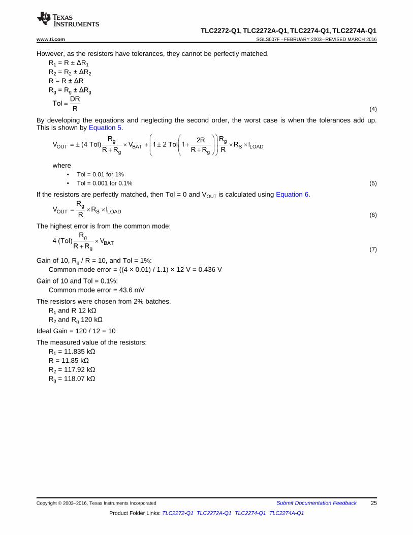
Submit Documentation FeedbackCopyright © 2003–2016, Texas Instruments Incorporated
However, as the resistors have tolerances, they cannot be perfectly matched.R1 = R ± ΔR1R2 = R2 ± ΔR2R = R ± ΔRRg = Rg ± ΔRg
(4)
By developing the equations and neglecting the second order, the worst case is when the tolerances add up.This is shown by Equation 5.
where• Tol = 0.01 for 1%• Tol = 0.001 for 0.1% (5)
If the resistors are perfectly matched, then Tol = 0 and VOUT is calculated using Equation 6.
(6)
The highest error is from the common mode:
(7)
Gain of 10, Rg / R = 10, and Tol = 1%:Common mode error = ((4 × 0.01) / 1.1) × 12 V = 0.436 V
Gain of 10 and Tol = 0.1%:Common mode error = 43.6 mV
The resistors were chosen from 2% batches.R1 and R 12 kΩR2 and Rg 120 kΩ
Ideal Gain = 120 / 12 = 10
The measured value of the resistors:R1 = 11.835 kΩR = 11.85 kΩR2 = 117.92 kΩRg = 118.07 kΩ
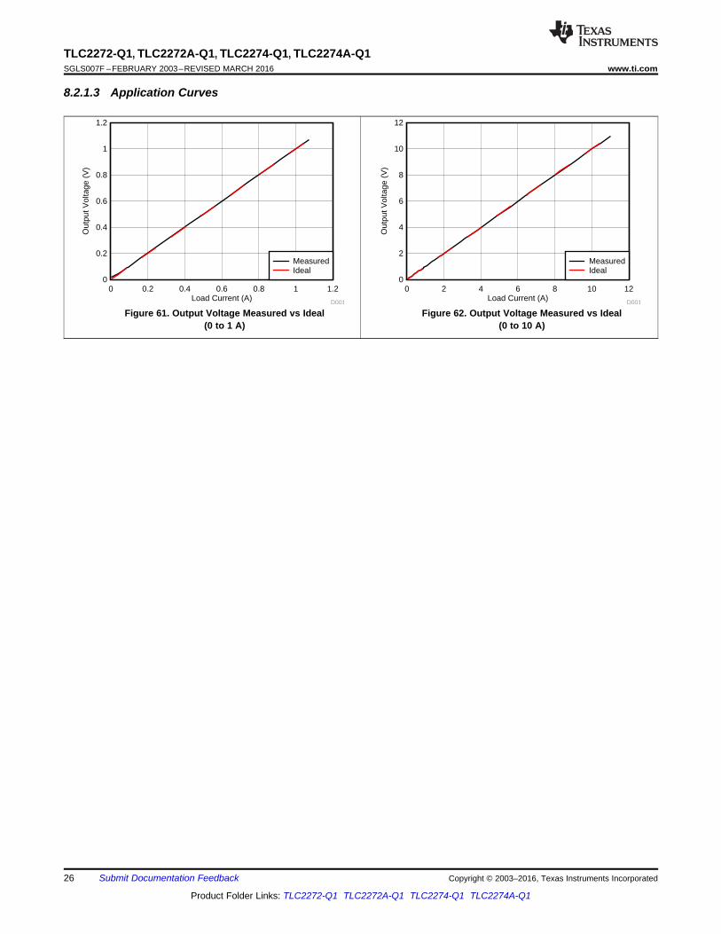
Load Current (A)
Out
put V
olta
ge (
V)
0 0.2 0.4 0.6 0.8 1 1.20
0.2
0.4
0.6
0.8
1
1.2
D001
MeasuredIdeal
Load Current (A)
Out
put V
olta
ge (
V)
0 2 4 6 8 10 120
2
4
6
8
10
12
D001
MeasuredIdeal
26
TLC2272-Q1, TLC2272A-Q1, TLC2274-Q1, TLC2274A-Q1SGLS007F –FEBRUARY 2003–REVISED MARCH 2016 www.ti.com
Product Folder Links: TLC2272-Q1 TLC2272A-Q1 TLC2274-Q1 TLC2274A-Q1
Submit Documentation Feedback Copyright © 2003–2016, Texas Instruments Incorporated
8.2.1.3 Application Curves
Figure 61. Output Voltage Measured vs Ideal(0 to 1 A)
Figure 62. Output Voltage Measured vs Ideal(0 to 10 A)

VOUT
NC
–IN
+IN
V–
NC
V+
OUT
NC
VS+
GND
RG
RIN
VS–(or GND for single supply)
GND
GND
Only needed fordual-supplyoperation
VIN
Run the input tracesas far away fromthe supply lines
as possible
Place componentsclose to device and toeach other to reduce
parasitic errors RF
Use low-ESR ceramicbypass capacitor
Ground (GND) plane on another layer
+
–
RIN
RG
VIN
RF
VOUT
27
TLC2272-Q1, TLC2272A-Q1, TLC2274-Q1, TLC2274A-Q1www.ti.com SGLS007F –FEBRUARY 2003–REVISED MARCH 2016
Product Folder Links: TLC2272-Q1 TLC2272A-Q1 TLC2274-Q1 TLC2274A-Q1
Submit Documentation FeedbackCopyright © 2003–2016, Texas Instruments Incorporated
9 Power Supply RecommendationsSupply voltage is 4.4 V to 16 V for single supply and ±2.2 V to ±8 V for dual. In the high-side sensing application,the supply is connected to a 12-V battery.
10 Layout
10.1 Layout GuidelinesThe TLC227x-Q1 is a wideband amplifier. To realize the full operational performance of the device, good highfrequency printed-circuit-board (PCB) layout practices are required. Low-loss 0.1-μF bypass capacitors must beconnected between each supply pin and ground as close to the device as possible. The bypass capacitor tracesmust be designed for minimum inductance.
10.2 Layout Examples
Figure 63. Schematic Representation
Figure 64. Operational Amplifier Board Layout for Noninverting Configuration

28
TLC2272-Q1, TLC2272A-Q1, TLC2274-Q1, TLC2274A-Q1SGLS007F –FEBRUARY 2003–REVISED MARCH 2016 www.ti.com
Product Folder Links: TLC2272-Q1 TLC2272A-Q1 TLC2274-Q1 TLC2274A-Q1
Submit Documentation Feedback Copyright © 2003–2016, Texas Instruments Incorporated
11 Device and Documentation Support
11.1 Documentation Support
11.1.1 Related DocumentationFor related documentation see the following:
Macromodeling of Integrated Circuit Operational Amplifiers, IEEE Journal of Solid-State Circuits, SC-9, 353(1974).
11.2 Related LinksThe table below lists quick access links. Categories include technical documents, support and communityresources, tools and software, and quick access to sample or buy.
Table 4. Related Links
PARTS PRODUCT FOLDER SAMPLE & BUY TECHNICALDOCUMENTS
TOOLS &SOFTWARE
SUPPORT &COMMUNITY
TLC2272-Q1 Click here Click here Click here Click here Click hereTLC2272A-Q1 Click here Click here Click here Click here Click hereTLC2274-Q1 Click here Click here Click here Click here Click hereTLC2274A-Q1 Click here Click here Click here Click here Click here
11.3 Community ResourcesThe following links connect to TI community resources. Linked contents are provided "AS IS" by the respectivecontributors. They do not constitute TI specifications and do not necessarily reflect TI's views; see TI's Terms ofUse.
TI E2E™ Online Community TI's Engineer-to-Engineer (E2E) Community. Created to foster collaborationamong engineers. At e2e.ti.com, you can ask questions, share knowledge, explore ideas and helpsolve problems with fellow engineers.
Design Support TI's Design Support Quickly find helpful E2E forums along with design support tools andcontact information for technical support.
11.4 TrademarksAdvanced LinCMOS, E2E are trademarks of Texas Instruments.MicroSim Parts, PSpice are trademarks of MicroSim.All other trademarks are the property of their respective owners.
11.5 Electrostatic Discharge CautionThese devices have limited built-in ESD protection. The leads should be shorted together or the device placed in conductive foamduring storage or handling to prevent electrostatic damage to the MOS gates.
11.6 GlossarySLYZ022 — TI Glossary.
This glossary lists and explains terms, acronyms, and definitions.
12 Mechanical, Packaging, and Orderable InformationThe following pages include mechanical, packaging, and orderable information. This information is the mostcurrent data available for the designated devices. This data is subject to change without notice and revision ofthis document. For browser-based versions of this data sheet, refer to the left-hand navigation.

PACKAGE OPTION ADDENDUM
www.ti.com 3-Sep-2015
Addendum-Page 1
PACKAGING INFORMATION
Orderable Device Status(1)
Package Type PackageDrawing
Pins PackageQty
Eco Plan(2)
Lead/Ball Finish(6)
MSL Peak Temp(3)
Op Temp (°C) Device Marking(4/5)
Samples
TLC2272AQDRG4Q1 ACTIVE SOIC D 8 2500 Green (RoHS& no Sb/Br)
CU NIPDAU Level-1-260C-UNLIM -40 to 125 2272AQ
TLC2272AQDRQ1 ACTIVE SOIC D 8 2500 Green (RoHS& no Sb/Br)
CU NIPDAU Level-1-260C-UNLIM -40 to 125 2272AQ
TLC2272AQPWRG4Q1 ACTIVE TSSOP PW 8 2000 Green (RoHS& no Sb/Br)
CU NIPDAU Level-1-260C-UNLIM -40 to 125 2272AQ
TLC2272AQPWRQ1 ACTIVE TSSOP PW 8 2000 Green (RoHS& no Sb/Br)
CU NIPDAU Level-1-260C-UNLIM -40 to 125 2272AQ
TLC2272QDRG4Q1 ACTIVE SOIC D 8 2500 Green (RoHS& no Sb/Br)
CU NIPDAU Level-1-260C-UNLIM -40 to 125 2272Q1
TLC2272QDRQ1 ACTIVE SOIC D 8 2500 Green (RoHS& no Sb/Br)
CU NIPDAU Level-1-260C-UNLIM -40 to 125 2272Q1
TLC2272QPWRG4Q1 ACTIVE TSSOP PW 8 2000 Green (RoHS& no Sb/Br)
CU NIPDAU Level-1-260C-UNLIM -40 to 125 2272Q1
TLC2272QPWRQ1 ACTIVE TSSOP PW 8 2000 Green (RoHS& no Sb/Br)
CU NIPDAU Level-1-260C-UNLIM -40 to 125 2272Q1
TLC2274AQDRG4Q1 ACTIVE SOIC D 14 2500 Green (RoHS& no Sb/Br)
CU NIPDAU Level-1-260C-UNLIM -40 to 125 2274AQ1
TLC2274AQDRQ1 ACTIVE SOIC D 14 2500 Green (RoHS& no Sb/Br)
CU NIPDAU Level-1-260C-UNLIM -40 to 125 2274AQ1
TLC2274AQPWRG4Q1 ACTIVE TSSOP PW 14 2000 Green (RoHS& no Sb/Br)
CU NIPDAU Level-1-260C-UNLIM -40 to 125 2274AQ1
TLC2274AQPWRQ1 ACTIVE TSSOP PW 14 2000 Green (RoHS& no Sb/Br)
CU NIPDAU Level-1-260C-UNLIM -40 to 125 2274AQ1
TLC2274QDRG4Q1 ACTIVE SOIC D 14 2500 Green (RoHS& no Sb/Br)
CU NIPDAU Level-1-260C-UNLIM -40 to 125 2274Q1
TLC2274QDRQ1 ACTIVE SOIC D 14 2500 Green (RoHS& no Sb/Br)
CU NIPDAU Level-1-260C-UNLIM -40 to 125 2274Q1
TLC2274QPWRG4Q1 ACTIVE TSSOP PW 14 2000 Green (RoHS& no Sb/Br)
CU NIPDAU Level-1-260C-UNLIM -40 to 125 2274Q1
TLC2274QPWRQ1 ACTIVE TSSOP PW 14 2000 Green (RoHS& no Sb/Br)
CU NIPDAU Level-1-260C-UNLIM -40 to 125 2274Q1
(1) The marketing status values are defined as follows:ACTIVE: Product device recommended for new designs.

PACKAGE OPTION ADDENDUM
www.ti.com 3-Sep-2015
Addendum-Page 2
LIFEBUY: TI has announced that the device will be discontinued, and a lifetime-buy period is in effect.NRND: Not recommended for new designs. Device is in production to support existing customers, but TI does not recommend using this part in a new design.PREVIEW: Device has been announced but is not in production. Samples may or may not be available.OBSOLETE: TI has discontinued the production of the device.
(2) Eco Plan - The planned eco-friendly classification: Pb-Free (RoHS), Pb-Free (RoHS Exempt), or Green (RoHS & no Sb/Br) - please check http://www.ti.com/productcontent for the latest availabilityinformation and additional product content details.TBD: The Pb-Free/Green conversion plan has not been defined.Pb-Free (RoHS): TI's terms "Lead-Free" or "Pb-Free" mean semiconductor products that are compatible with the current RoHS requirements for all 6 substances, including the requirement thatlead not exceed 0.1% by weight in homogeneous materials. Where designed to be soldered at high temperatures, TI Pb-Free products are suitable for use in specified lead-free processes.Pb-Free (RoHS Exempt): This component has a RoHS exemption for either 1) lead-based flip-chip solder bumps used between the die and package, or 2) lead-based die adhesive used betweenthe die and leadframe. The component is otherwise considered Pb-Free (RoHS compatible) as defined above.Green (RoHS & no Sb/Br): TI defines "Green" to mean Pb-Free (RoHS compatible), and free of Bromine (Br) and Antimony (Sb) based flame retardants (Br or Sb do not exceed 0.1% by weightin homogeneous material)
(3) MSL, Peak Temp. - The Moisture Sensitivity Level rating according to the JEDEC industry standard classifications, and peak solder temperature.
(4) There may be additional marking, which relates to the logo, the lot trace code information, or the environmental category on the device.
(5) Multiple Device Markings will be inside parentheses. Only one Device Marking contained in parentheses and separated by a "~" will appear on a device. If a line is indented then it is a continuationof the previous line and the two combined represent the entire Device Marking for that device.
(6) Lead/Ball Finish - Orderable Devices may have multiple material finish options. Finish options are separated by a vertical ruled line. Lead/Ball Finish values may wrap to two lines if the finishvalue exceeds the maximum column width.
Important Information and Disclaimer:The information provided on this page represents TI's knowledge and belief as of the date that it is provided. TI bases its knowledge and belief on informationprovided by third parties, and makes no representation or warranty as to the accuracy of such information. Efforts are underway to better integrate information from third parties. TI has taken andcontinues to take reasonable steps to provide representative and accurate information but may not have conducted destructive testing or chemical analysis on incoming materials and chemicals.TI and TI suppliers consider certain information to be proprietary, and thus CAS numbers and other limited information may not be available for release.
In no event shall TI's liability arising out of such information exceed the total purchase price of the TI part(s) at issue in this document sold by TI to Customer on an annual basis.
OTHER QUALIFIED VERSIONS OF TLC2272-Q1, TLC2272A-Q1, TLC2274-Q1, TLC2274A-Q1 :
• Catalog: TLC2272, TLC2272A, TLC2274, TLC2274A
• Enhanced Product: TLC2272A-EP, TLC2274-EP, TLC2274A-EP
• Military: TLC2272M, TLC2272AM, TLC2274M, TLC2274AM
PACKAGE OPTION ADDENDUM
www.ti.com 3-Sep-2015
Addendum-Page 3
NOTE: Qualified Version Definitions:
• Catalog - TI's standard catalog product
• Enhanced Product - Supports Defense, Aerospace and Medical Applications
• Military - QML certified for Military and Defense Applications

TAPE AND REEL INFORMATION
*All dimensions are nominal
Device PackageType
PackageDrawing
Pins SPQ ReelDiameter
(mm)
ReelWidth
W1 (mm)
A0(mm)
B0(mm)
K0(mm)
P1(mm)
W(mm)
Pin1Quadrant
TLC2272AQPWRG4Q1 TSSOP PW 8 2000 330.0 12.4 7.0 3.6 1.6 8.0 12.0 Q1
TLC2272AQPWRQ1 TSSOP PW 8 2000 330.0 12.4 7.0 3.6 1.6 8.0 12.0 Q1
TLC2272QPWRG4Q1 TSSOP PW 8 2000 330.0 12.4 7.0 3.6 1.6 8.0 12.0 Q1
TLC2272QPWRQ1 TSSOP PW 8 2000 330.0 12.4 7.0 3.6 1.6 8.0 12.0 Q1
TLC2274AQPWRG4Q1 TSSOP PW 14 2000 330.0 12.4 6.9 5.6 1.6 8.0 12.0 Q1
TLC2274AQPWRQ1 TSSOP PW 14 2000 330.0 12.4 6.9 5.6 1.6 8.0 12.0 Q1
TLC2274QPWRG4Q1 TSSOP PW 14 2000 330.0 12.4 6.9 5.6 1.6 8.0 12.0 Q1
TLC2274QPWRQ1 TSSOP PW 14 2000 330.0 12.4 6.9 5.6 1.6 8.0 12.0 Q1
PACKAGE MATERIALS INFORMATION
www.ti.com 16-Oct-2016
Pack Materials-Page 1
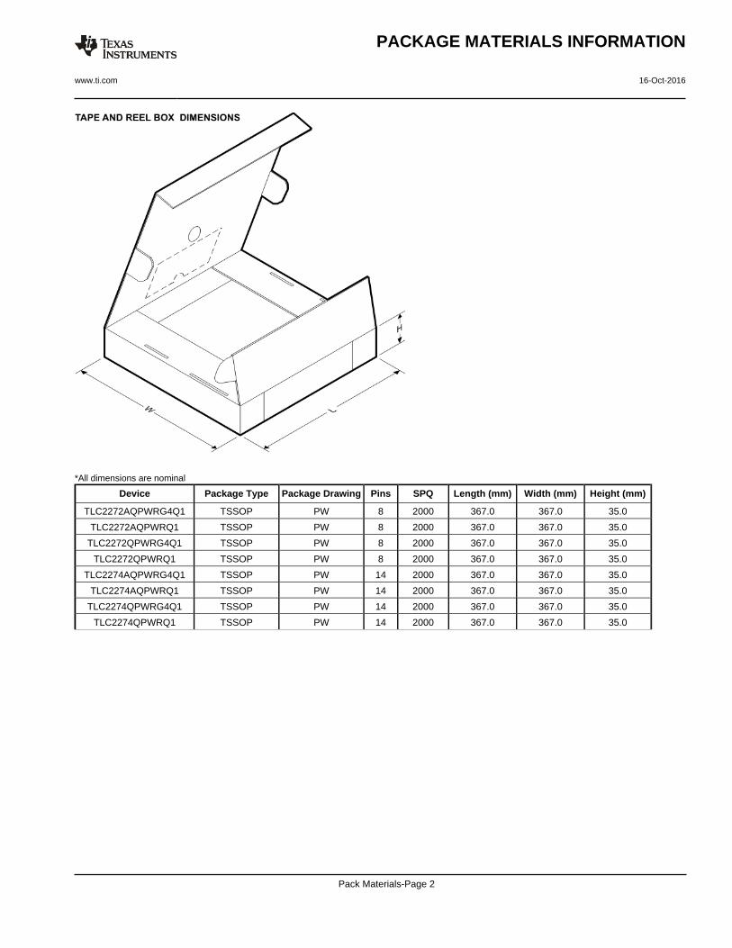
*All dimensions are nominal
Device Package Type Package Drawing Pins SPQ Length (mm) Width (mm) Height (mm)
TLC2272AQPWRG4Q1 TSSOP PW 8 2000 367.0 367.0 35.0
TLC2272AQPWRQ1 TSSOP PW 8 2000 367.0 367.0 35.0
TLC2272QPWRG4Q1 TSSOP PW 8 2000 367.0 367.0 35.0
TLC2272QPWRQ1 TSSOP PW 8 2000 367.0 367.0 35.0
TLC2274AQPWRG4Q1 TSSOP PW 14 2000 367.0 367.0 35.0
TLC2274AQPWRQ1 TSSOP PW 14 2000 367.0 367.0 35.0
TLC2274QPWRG4Q1 TSSOP PW 14 2000 367.0 367.0 35.0
TLC2274QPWRQ1 TSSOP PW 14 2000 367.0 367.0 35.0
PACKAGE MATERIALS INFORMATION
www.ti.com 16-Oct-2016
Pack Materials-Page 2


www.ti.com
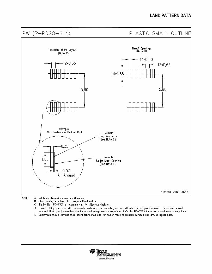
PACKAGE OUTLINE
C
TYP6.66.2
1.2 MAX
6X 0.65
8X 0.300.19
2X1.95
0.150.05
(0.15) TYP
0 - 8
0.25GAGE PLANE
0.750.50
A
NOTE 3
3.12.9
BNOTE 4
4.54.3
4221848/A 02/2015
TSSOP - 1.2 mm max heightPW0008ASMALL OUTLINE PACKAGE
NOTES: 1. All linear dimensions are in millimeters. Any dimensions in parenthesis are for reference only. Dimensioning and tolerancing per ASME Y14.5M. 2. This drawing is subject to change without notice. 3. This dimension does not include mold flash, protrusions, or gate burrs. Mold flash, protrusions, or gate burrs shall not exceed 0.15 mm per side. 4. This dimension does not include interlead flash. Interlead flash shall not exceed 0.25 mm per side.5. Reference JEDEC registration MO-153, variation AA.
18
0.1 C A B
54
PIN 1 IDAREA
SEATING PLANE
0.1 C
SEE DETAIL A
DETAIL ATYPICAL
SCALE 2.800
www.ti.com
EXAMPLE BOARD LAYOUT
(5.8)
0.05 MAXALL AROUND
0.05 MINALL AROUND
8X (1.5)8X (0.45)
6X (0.65)
(R )TYP
0.05
4221848/A 02/2015
TSSOP - 1.2 mm max heightPW0008ASMALL OUTLINE PACKAGE
SYMM
SYMM
LAND PATTERN EXAMPLESCALE:10X
1
45
8
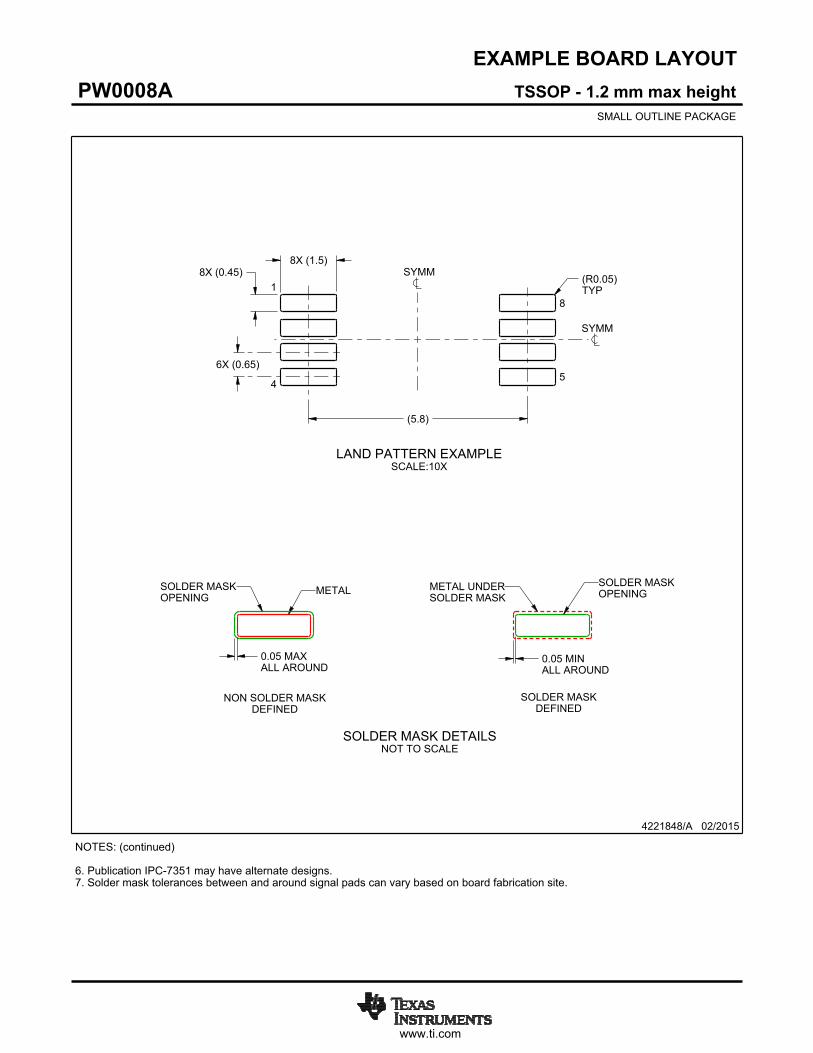
NOTES: (continued) 6. Publication IPC-7351 may have alternate designs. 7. Solder mask tolerances between and around signal pads can vary based on board fabrication site.
METALSOLDER MASKOPENING
NON SOLDER MASKDEFINED
SOLDER MASK DETAILSNOT TO SCALE
SOLDER MASKOPENING
METAL UNDERSOLDER MASK
SOLDER MASKDEFINED

www.ti.com
EXAMPLE STENCIL DESIGN
(5.8)
6X (0.65)
8X (0.45)8X (1.5)
(R ) TYP0.05
4221848/A 02/2015
TSSOP - 1.2 mm max heightPW0008ASMALL OUTLINE PACKAGE
NOTES: (continued) 8. Laser cutting apertures with trapezoidal walls and rounded corners may offer better paste release. IPC-7525 may have alternate design recommendations. 9. Board assembly site may have different recommendations for stencil design.
SYMM
SYMM
1
45
8
SOLDER PASTE EXAMPLEBASED ON 0.125 mm THICK STENCIL
SCALE:10X


IMPORTANT NOTICE
Texas Instruments Incorporated and its subsidiaries (TI) reserve the right to make corrections, enhancements, improvements and otherchanges to its semiconductor products and services per JESD46, latest issue, and to discontinue any product or service per JESD48, latestissue. Buyers should obtain the latest relevant information before placing orders and should verify that such information is current andcomplete. All semiconductor products (also referred to herein as “components”) are sold subject to TI’s terms and conditions of salesupplied at the time of order acknowledgment.TI warrants performance of its components to the specifications applicable at the time of sale, in accordance with the warranty in TI’s termsand conditions of sale of semiconductor products. Testing and other quality control techniques are used to the extent TI deems necessaryto support this warranty. Except where mandated by applicable law, testing of all parameters of each component is not necessarilyperformed.TI assumes no liability for applications assistance or the design of Buyers’ products. Buyers are responsible for their products andapplications using TI components. To minimize the risks associated with Buyers’ products and applications, Buyers should provideadequate design and operating safeguards.TI does not warrant or represent that any license, either express or implied, is granted under any patent right, copyright, mask work right, orother intellectual property right relating to any combination, machine, or process in which TI components or services are used. Informationpublished by TI regarding third-party products or services does not constitute a license to use such products or services or a warranty orendorsement thereof. Use of such information may require a license from a third party under the patents or other intellectual property of thethird party, or a license from TI under the patents or other intellectual property of TI.Reproduction of significant portions of TI information in TI data books or data sheets is permissible only if reproduction is without alterationand is accompanied by all associated warranties, conditions, limitations, and notices. TI is not responsible or liable for such altereddocumentation. Information of third parties may be subject to additional restrictions.Resale of TI components or services with statements different from or beyond the parameters stated by TI for that component or servicevoids all express and any implied warranties for the associated TI component or service and is an unfair and deceptive business practice.TI is not responsible or liable for any such statements.Buyer acknowledges and agrees that it is solely responsible for compliance with all legal, regulatory and safety-related requirementsconcerning its products, and any use of TI components in its applications, notwithstanding any applications-related information or supportthat may be provided by TI. Buyer represents and agrees that it has all the necessary expertise to create and implement safeguards whichanticipate dangerous consequences of failures, monitor failures and their consequences, lessen the likelihood of failures that might causeharm and take appropriate remedial actions. Buyer will fully indemnify TI and its representatives against any damages arising out of the useof any TI components in safety-critical applications.In some cases, TI components may be promoted specifically to facilitate safety-related applications. With such components, TI’s goal is tohelp enable customers to design and create their own end-product solutions that meet applicable functional safety standards andrequirements. Nonetheless, such components are subject to these terms.No TI components are authorized for use in FDA Class III (or similar life-critical medical equipment) unless authorized officers of the partieshave executed a special agreement specifically governing such use.Only those TI components which TI has specifically designated as military grade or “enhanced plastic” are designed and intended for use inmilitary/aerospace applications or environments. Buyer acknowledges and agrees that any military or aerospace use of TI componentswhich have not been so designated is solely at the Buyer's risk, and that Buyer is solely responsible for compliance with all legal andregulatory requirements in connection with such use.TI has specifically designated certain components as meeting ISO/TS16949 requirements, mainly for automotive use. In any case of use ofnon-designated products, TI will not be responsible for any failure to meet ISO/TS16949.
Products ApplicationsAudio www.ti.com/audio Automotive and Transportation www.ti.com/automotiveAmplifiers amplifier.ti.com Communications and Telecom www.ti.com/communicationsData Converters dataconverter.ti.com Computers and Peripherals www.ti.com/computersDLP® Products www.dlp.com Consumer Electronics www.ti.com/consumer-appsDSP dsp.ti.com Energy and Lighting www.ti.com/energyClocks and Timers www.ti.com/clocks Industrial www.ti.com/industrialInterface interface.ti.com Medical www.ti.com/medicalLogic logic.ti.com Security www.ti.com/securityPower Mgmt power.ti.com Space, Avionics and Defense www.ti.com/space-avionics-defenseMicrocontrollers microcontroller.ti.com Video and Imaging www.ti.com/videoRFID www.ti-rfid.comOMAP Applications Processors www.ti.com/omap TI E2E Community e2e.ti.comWireless Connectivity www.ti.com/wirelessconnectivity
Mailing Address: Texas Instruments, Post Office Box 655303, Dallas, Texas 75265Copyright © 2016, Texas Instruments Incorporated