three-dimensional colloidal interference lithography
TRANSCRIPT

Three-dimensional colloidal interferencelithography
Hironori Nagai, Austen Poteet, Xu A Zhang and Chih-Hao Chang
Department of Mechanical and Aerospace Engineering, North Carolina State University, Raleigh, NC27695, United States of America
E-mail: [email protected]
Received 9 December 2016, revised 20 January 2017Accepted for publication 3 February 2017Published 23 February 2017
AbstractLight interactions with colloidal particles can generate a variety of complex three-dimensional(3D) intensity patterns, which can be utilized for nanolithography. The study of particle–lightinteractions can add more types of intensity patterns by manipulating key factors. Here weinvestigate a novel 3D nanolithography technique using colloidal particles under two-beamcoherent illuminations. The fabricated 3D nanostructures are hollow, nested within periodicstructures, and possess multiple chamber geometry. The effects of incident angles and particlesize on the fabricated nanostructures were examined. The relative phase shift between particleposition and interference pattern is identified as another significant parameter influencing theresultant nanostructures. A numerical model has been developed to show the evolution ofnanostructure geometry with phase shifts, and experimental studies confirm the simulationresults. Through the introduction of single colloidal particles, the fabrication capability ofLloyd’s mirror interference can now be extended to fabrication of 3D nanostructure withcomplex shell geometry. The fabricated hollow nanostructures with grating background couldfind potential applications in the area of photonics, drug delivery, and nanofluidics.
Keywords: nanolithography, three-dimensional nanostructures, colloids, self-assembly, inter-ference lithography
(Some figures may appear in colour only in the online journal)
Introduction
Three-dimensional (3D) nanostructures have found manyinteresting applications in the area of photonics and plasmonics[1–5], energy [6, 7], drug delivery [8–13], and others. Forcertain applications, different types of nanostructures areusually needed. For example, drug delivery applicationsrequire hollow nanostructures while photonic applications needperiodic nanostructures. Therefore, a large variety of fabrica-tion techniques have been developed, and they can be generallycategorized as ‘top-down’ and ‘bottom-up’ techniques. ‘Top-down’ techniques, such as electron-beam lithography [14],two-photon polymerization [15–18], and focused ion beammilling [19], usually require complex hardware systems.Although complex 3D nanostructures can be fabricated usingthese techniques, throughput is relatively low and process canbe costly. In ‘bottom-up’ techniques, colloidal particle self-
assembly can serve as a representative technique with char-acteristics of low cost and high throughput, and is promisingfor scaled-up manufacturing. Colloidal particles can act asbuilding elements and be assembled into 3D nanostructuressuch as opal structures [20]. In addition, colloidal particlearrays have been used as physical masks for metal-assistedchemical etching and focusing element for laser ablation [21–23]. However, the presence of defects and the low variety ofassembly architectures are limiting factors in colloidal particleself-assembly. Recently, there has been progress in roll-to-rollcoating of colloidal particle assemblies with the potential toscale up 3D nanostructure fabrication [24].
The combination of ‘top-down’ and ‘bottom-up’ techni-ques takes advantage of both techniques, and has enabledmore complex nanostructures. In our previous work [25–27],colloidal particle assemblies were employed as optical phasemasks for 3D nanolithography. For example, regular colloidal
Nanotechnology
Nanotechnology 28 (2017) 125302 (6pp) https://doi.org/10.1088/1361-6528/aa5e3f
0957-4484/17/125302+06$33.00 © 2017 IOP Publishing Ltd Printed in the UK1

particle assemblies modulate particle–light interactions andcan produce periodic 3D light distributions by Talbot effects[25]. Mie scattering of single isolated particles can also beharnessed to produce normal and oblique ‘nano-volcanoes’[26, 27]. In addition, 3D nanostructures with complex sym-metries were achieved using sequential symmetric multipleexposures. The resultant 3D nanostructures are from theincoherent summation of light scattering intensity from eachexposure.
In this work, we investigate the particle–light interactionswith coherent two-beam exposures for 3D nanolithography.In this approach, two mutually coherent laser beams areilluminated on an isolated sphere to produce a complexintensity profile. Since the interference pattern of the twoincident beams is periodic in one dimension, the relativephase between the fringe pattern and colloidal particle posi-tion becomes an added lithography parameter to determineresulting nanostructure geometry, in addition to incidenceangle, colloidal particle diameter, and exposure dosage. As aresult of the phase difference, the chamber geometry insidethe 3D nanostructure can be varied. To model the lithographyexposure and predict the fabricated results, a numerical modelhas been developed using finite-difference time-domain(FDTD) simulation and binary resist model [26, 27]. ALloyd’s mirror interference lithography system, well knownfor the fabrication of 1D and 2D periodic nanostructures withhigh resolution [28, 29], provides the coherent two-beamilluminations. With the incorporation of coherent illumina-tions, we are able to extend the fabrication capability ofcolloidal 3D nanolithography.
Methods
The proposed fabrication process is depicted in figure 1,where a single isolated colloidal particle is illuminated using a
Lloyd’s mirror interference lithography system. In this setup,single ultraviolet (UV) illumination is split into two sym-metric, mutually coherent interfering beams. Without thepresence of the colloidal particle, a periodic sinusoidalintensity pattern can be generated within the photoresist layer.The presence of colloidal particles on the photoresist surfacemodulates the light intensity distribution locally through lightscattering, as illustrated in figure 1(b) from FDTD simula-tions. The phase difference between the particle position andthe intensity maximum is denoted by j, which is a key factorin defining resultant 3D nanostructures.
In all experiments, silicon substrates were used to preparefor the samples. A thin layer of photoresist (Sumitomo PFI-88A7) with the thickness of 1 μm was spin-coated on a siliconwafer to record light intensity pattern. Polystyrene sphereswith 1 and 2 μm diameters (Polysciences, inc. PolybeadMicrospheres in 2.5% aqueous solution) were spin-coated onphotoresist with 1000–2000 rpm for 1 min. The resist samplewas dipped in a developer solution (Microposit MF CD-26)and then in deionized water to treat the surface beforeassembly. The exposures were conducted using a Lloyd’smirror interference lithography system and a 325 nm wave-length HeCd laser (KIMMON KOHA., ltd) to create thedesired coherent condition. The samples were exposed withdosages of 60–100 mJ cm−2, which corresponds to exposuretime in the order of 20–30 min. After exposure, the nano-spheres were removed by sonication and the photoresist wasdeveloped by immersing into developer solution (MicropositMF-CD26) for 2 min. The fabricated samples were char-acterized using a SEM (JEOL 6400 F) for top and crosssection views.
In order to examine the evolution of 3D nanostructureswith different phase shifts, the resultant 3D nanostructurescan be predicted using FDTD simulation combined withbinary resist model [26, 27]. FDTD modeling was performedusing the free, open-source software MEEP [30]. To create
Figure 1. (a) Fabrication process of colloidal interference lithography. (b) FDTD simulation showing a cross section of the 3D intensitypattern produced by TE-polarized UV light and a single nanosphere for 0 and π phase shifts. Red and white indicate high and low intensities,respectively.
2
Nanotechnology 28 (2017) 125302 H Nagai et al
two oblique incident sources in the simulation, a periodicboundary condition was used to capture the interferencebetween the incident and the reflecting beams. Therefore thesimulation domain must be an integer multiple of the periodof the interference field pattern, determined by the equation,
( )l qL = sin , where L is the period, l is the wavelength,and q is the incident angle. The electric field resulting fromthe FDTD model was then compared to a threshold value tomodel a binary photoresist behavior. The intensity valuesfalling above the threshold were removed to model positivephotoresist, leaving the resulting structure in 3D space. This3D structure is represented using Matlab’s isosurface andpatch functions, which introduce built-in smoothing based onthe intensity of the remaining values.
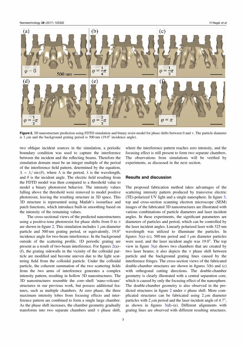
The cross-sectional views of the predicted nanostructuresusing a positive-tone photoresist for phase shifts from 0 to π
are shown in figure 2. This simulation includes 1 μm diameterparticle and 500 nm grating period, or equivalently, 19.0°incidence angle for two-beam interference. In the backgroundoutside of the scattering profile, 1D periodic grating arepresent as a result of two-beam interference. For figures 2(a)–(f), the grating sidewalls in the vicinity of the colloidal par-ticle are modified and become uneven due to the light scat-tering field from the colloidal particle. Under the colloidalparticle, the coherent summation of the two scattering fieldsfrom the two arms of interference generates a complexintensity pattern, resulting in hollow 3D nanostructures. The3D nanostructures resemble the core–shell ‘nano-volcano’structures in our previous work, but possess additional fea-tures, such as multiple chambers. At zero phase, the threemaximum intensity lobes from focusing effects and inter-ference pattern are combined to form a single large chamber.As the phase shift increases, the chamber geometry graduallytransforms into two separate chambers until π phase shift,
where the interference pattern reaches zero intensity, and thefocusing effect is still present to form two separate chambers.The observations from simulations will be verified byexperiments, as discussed in the next section.
Results and discussion
The proposed fabrication method takes advantages of thescattering intensity pattern produced by transverse electric(TE)-polarized UV light and a single nanosphere. In figure 3,top and cross-section scanning electron microscope (SEM)images of the fabricated 3D nanostructures are illustrated withvarious combinations of particle diameters and laser incidentangles. In these experiments, the significant parameters arediameters of particles and period, which can be controlled bythe laser incident angles. Linearly polarized laser with 325 nmwavelength was utilized to illuminate the particles. Infigures 3(a)–(c), 500 nm period and 1 μm diameter particleswere used, and the laser incident angle was 19.0°. The topview in figure 3(a) shows two chambers that are created bytwo laser beams; it also depicts the π phase shift betweenparticle and the background grating lines caused by theinterference fringes. The cross-section views of the fabricateddouble-chamber structures are shown in figures 3(b) and (c)with orthogonal cutting directions. The double-chambergeometry is clearly illustrated with a central separation core,which is caused by only the focusing effect of the nanosphere.The double-chamber geometry is also observed in the pre-dicted structures in figure 2 under π phase shift. More com-plicated structures can be fabricated using 2 μm diameterparticles with 2 μm period and the laser incident angle of 4.7°,as shown in figures 3(d)–(e). Different alignments withgrating lines are observed with different resulting structures.
Figure 2. 3D nanostructure prediction using FDTD simulation and binary resist model for phase shifts between 0 and π. The particle diameteris 1 μm and the background grating period is 500 nm (19.0° incidence angle).
3
Nanotechnology 28 (2017) 125302 H Nagai et al
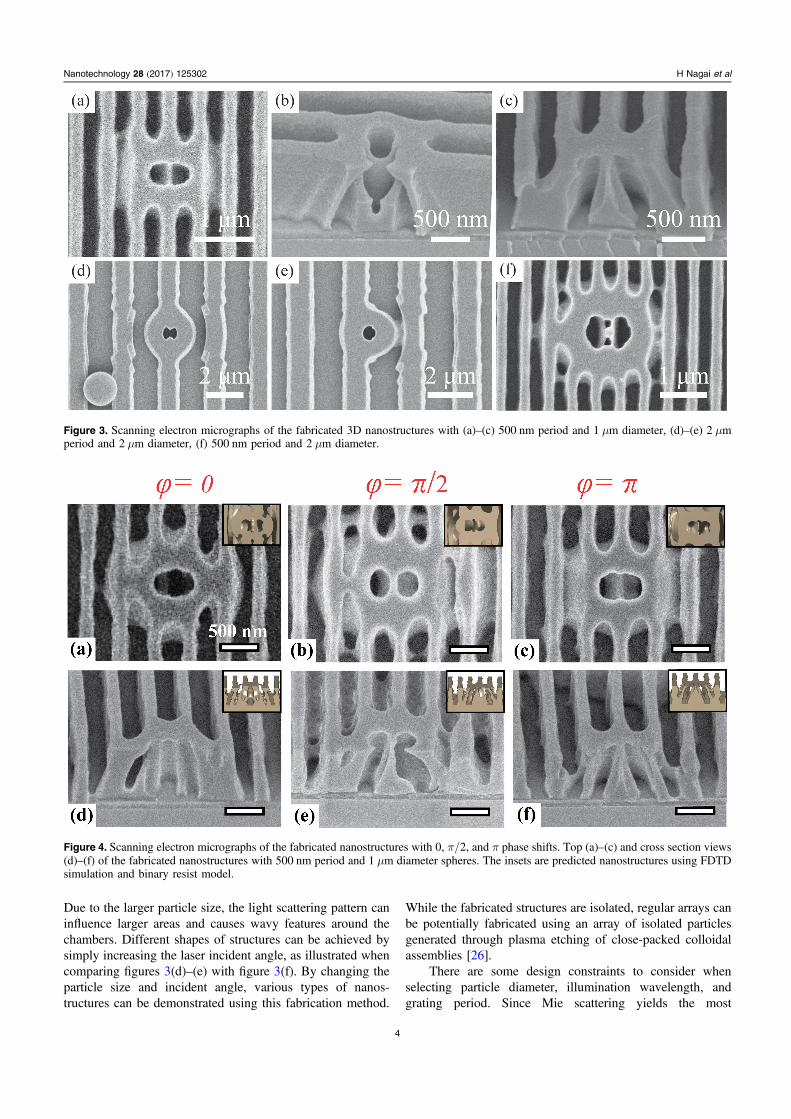
Due to the larger particle size, the light scattering pattern caninfluence larger areas and causes wavy features around thechambers. Different shapes of structures can be achieved bysimply increasing the laser incident angle, as illustrated whencomparing figures 3(d)–(e) with figure 3(f). By changing theparticle size and incident angle, various types of nanos-tructures can be demonstrated using this fabrication method.
While the fabricated structures are isolated, regular arrays canbe potentially fabricated using an array of isolated particlesgenerated through plasma etching of close-packed colloidalassemblies [26].
There are some design constraints to consider whenselecting particle diameter, illumination wavelength, andgrating period. Since Mie scattering yields the most
Figure 3. Scanning electron micrographs of the fabricated 3D nanostructures with (a)–(c) 500 nm period and 1 μm diameter, (d)–(e) 2 μmperiod and 2 μm diameter, (f) 500 nm period and 2 μm diameter.
Figure 4. Scanning electron micrographs of the fabricated nanostructures with 0, π/2, and π phase shifts. Top (a)–(c) and cross section views(d)–(f) of the fabricated nanostructures with 500 nm period and 1 μm diameter spheres. The insets are predicted nanostructures using FDTDsimulation and binary resist model.
4
Nanotechnology 28 (2017) 125302 H Nagai et al

interesting angular intensity patterns [26], the particle istypically selected to be similar or slightly larger than theexposure wavelength. Smaller particles will result in shell-likegeometries, as shown in figures 3(a)–(c), while larger particleswill result in disk-like geometry, as illustrated in figures 3(d)–(f). The grating period, which depends on illuminationwavelength and incident angle, can then be selected inde-pendently to incorporate the structure. Further experimentswere focused on 500 nm and 1 μm grating period with 1 μmdiameter nanosphere to examine the phase shift dependenceof the nanostructures.
Based on the location of nanosphere under interferencelithography, different phase shift patterns can be achievedsuch as under phase shifts of 0, π/2 and π, as shown infigure 4. The SEM images show both top views (a), (b), and(c) and cross-section views (d), (e), and (f) of the 3Dnanostructures with phase shifts of 0, π/2 and π, respectively.The inset diagrams in figure 4 show the simulated structures.Figures 4(a) and (d) show only one chamber that is created bytwo laser beams. Because the laser intensity is the highestwith zero phase shift, the intensity under the nanosphere isfocused, matching well with figure 2(a). In figures 4(b) and(e), two unsymmetrical chambers were observed because theintensity patterns under the nanosphere are not evenlybalanced with π/2 phase shift. In another case, two symmetricchambers were observed with π phase shift in figures 4(c) and(f). A separation core is observed in the middle of thestructure that isolates two symmetric chambers as a result ofdestructive interference.
Figure 5 shows the fabrication results of 1 μm diameterspheres and 1 μm period, with the incident angle of 9.4° andphase shifts of 0, π/2, and π. Similar changes in structuresdue to phase shift were expected to be observed; however,different shapes of structures are fabricated due to the largerperiod. Since the laser incident angle is smaller than theprevious experiment, the width of the scattering intensitypatterns under nanosphere is narrower as well. In figure 5(a),there is one hollow chamber without any complex structures.For π/2 phase shift, separate chamber cannot be observed.With π phase shift sample shown in figure 5(f), multiplechambers and core–shell structures can be generated by usingsmaller laser incident angle. In smaller laser incident angles,the light intensity distribution resembles the normal incidencecase in our previous work, and produce core–shell hollow 3Dnanostructures.
Conclusion
In this work, 3D colloidal interference lithography undercoherent two-beam exposure is proposed, and differentshapes of 3D nanostructures can be fabricated with variouslaser incident angles, particle diameters, and phase shifts.FDTD simulation and binary resist model are used to predictthe fabricated 3D nanostructures, and provide guidance on theevolution of nanostructures with phase shifts. The scatteringintensity under the nanosphere, which can be controlled bychanging the phase shifts, has a significant contribution to the
Figure 5. Scanning electron micrographs of the fabricated nanostructures with 0, π/2, and π phase shifts. Top (a)–(c) and cross section views(d)–(f) of the fabricated nanostructures with 1 μm period and 1 μm diameter spheres. The insets are predicted nanostructures using FDTDsimulation and binary resist model.
5
Nanotechnology 28 (2017) 125302 H Nagai et al

different nanostructures, as demonstrated by our experimentalresults. The proposed colloidal interference lithographytechnique can create both symmetrical and unsymmetricalnanostructures with multiple chambers. In addition to phaseshifts, the shapes of chambers can also be controlled by laserincident angle and nanosphere diameter. Future work willfocus on methods to precisely and uniformly control thenanosphere position in an ordered array to achieve desiredphase shifts and yield different types of structures over largeareas. The fabricated double-chamber nanostructures couldfind potential applications in photonics, drug delivery, andnanofluidics.
Acknowledgments
This work was performed in part at the NCSU Nanofabrica-tion Facility (NNF) and the Analytical InstrumentationFacility (AIF), members of the North Carolina ResearchTriangle Nanotechnology Network (RTNN), which is sup-ported by the National Science Foundation (Grant ECCS-1542015) as part of the National Nanotechnology Coordi-nated Infrastructure (NNCI). This work was supported by aNASA Office of the Chief Technologist’s Space TechnologyResearch Opportunity—Early Career Faculty grant (grantNNX12AQ46G) and NSF Faculty Early Career Development(CAREER) Program (grant CMMI#1552424).
References
[1] Lin S Y et al 1998 A three-dimensional photonic crystaloperating at infrared wavelengths Nature 394 251–3
[2] Noda S, Tomoda K, Yamamoto N and Chutinan A 2000 Fullthree-dimensional photonic bandgap crystals at near-infraredwavelengths Science 289 604–6
[3] Qi M et al 2004 A three-dimensional optical photonic crystalwith designed point defects Nature 429 538–42
[4] De Angelis F et al 2013 3D hollow nanostructures as buildingblocks for multifunctional plasmonics Nano Lett. 13 3553–8
[5] Ai B, Yu Y, Möhwald H and Zhang G 2013 Responsivemonochromatic color display based on nanovolcano arraysAdv. Opt. Mater. 1 724–31
[6] Fan Z et al 2009 Three-dimensional nanopillar-arrayphotovoltaics on low-cost and flexible substrates Nat. Mater.8 648–53
[7] Zhang H, Yu X and Braun P V 2011 Three-dimensionalbicontinuous ultrafast-charge and -discharge bulk batteryelectrodes Nat. Nanotechnol. 6 277–81
[8] (David) Lou X W, Archer L A and Yang Z 2008 Hollowmicro-/nanostructures: synthesis and applications Adv.Mater. 20 3987–4019
[9] Yavuz M S et al 2009 Gold nanocages covered by smartpolymers for controlled release with near-infrared light Nat.Mater. 8 935–9
[10] Moon G D et al 2011 A new theranostic system based on goldnanocages and phase-change materials with unique features
for photoacoustic imaging and controlled release J. Am.Chem. Soc. 133 4762–5
[11] Peer E, Artzy-Schnirman A, Gepstein L and Sivan U 2012Hollow nanoneedle array and its utilization for repeatedadministration of biomolecules to the same cells ACS Nano6 4940–6
[12] Prausnitz M R, Mitragotri S and Langer R 2004 Current statusand future potential of transdermal drug delivery Nat. Rev.Drug Discov. 3 115–24
[13] Prausnitz M R and Langer R 2008 Transdermal drug deliveryNat. Biotechnol. 26 1261–8
[14] Yamazaki K and Yamaguchi H 2008 Three-dimensionalalignment with 10 nm order accuracy in electron-beamlithography on rotated sample for three-dimensionalnanofabrication J. Vac. Sci. Technol. B 26 2529–33
[15] Maruo S, Nakamura O and Kawata S 1997 Three-dimensionalmicrofabrication with two-photon-absorbedphotopolymerization Opt. Lett. 22 132–4
[16] Cumpston B H et al 1999 Two-photon polymerizationinitiators for three-dimensional optical data storage andmicrofabrication Nature 398 51–4
[17] Kawata S, Sun H-B, Tanaka T and Takada K 2001 Finerfeatures for functional microdevices Nature 412 697–8
[18] Haske W et al 2007 65 nm feature sizes using visiblewavelength 3D multiphoton lithography Opt. Express 153426–36
[19] Jeon J, Floresca H C and Kim M J 2010 Fabrication ofcomplex three-dimensional nanostructures using focused ionbeam and nanomanipulation J. Vac. Sci. Technol. B 28549–53
[20] Gates B, Qin D and Xia Y 1999 Assembly of nanoparticles intoopaline structures over large areas Adv. Mater. 11 466–9
[21] Brodoceanu D, Alhmoud H Z, Elnathan R, Delalat B,Voelcker N H and Kraus T 2016 Fabrication of siliconnanowire arrays by near-field laser ablation and metal-assisted chemical etching Nanotechnology 27 075301
[22] Choi W K, Liew T H, Dawood M K, Smith H I,Thompson C V and Hong M H 2008 Synthesis of siliconnanowires and nanofin arrays using interference lithographyand catalytic etching Nano Lett. 8 3799–802
[23] Huang Z, Fang H and Zhu J 2007 Fabrication of siliconnanowire arrays with controlled diameter, length, anddensity Adv. Mater. 19 744–8
[24] Li X and Gilchrist J F 2016 Large-area nanoparticle films bycontinuous automated langmuir–blodgett assembly anddeposition Langmuir 32 1220–6
[25] Chang C-H et al 2011 From two-dimensional colloidal self-assembly to three-dimensional nanolithography Nano Lett.11 2533–7
[26] Zhang X A, Elek J and Chang C-H 2013 Three-dimensionalnanolithography using light scattering from colloidalparticles ACS Nano 7 6212–8
[27] Zhang X A, Dai B, Xu Z and Chang C-H 2015 Sculptingasymmetric, hollow-core, three-dimensional nanostructuresusing colloidal particles Small 11 1285–92
[28] Smith H I 2001 Low cost nanolithography with nanoaccuracyPhysica E 11 104–9
[29] Bagal A and Chang C-H 2013 Fabrication of subwavelengthperiodic nanostructures using liquid immersion Lloyd’smirror interference lithography Opt. Lett. 38 2531
[30] Oskooi A F, Roundy D, Ibanescu M, Bermel P,Joannopoulos J D and Johnson S G 2010 Meep: a flexiblefree-software package for electromagnetic simulations by theFDTD method Comput. Phys. Commun. 181 687–702
6
Nanotechnology 28 (2017) 125302 H Nagai et al