thin-film silicon solar cells: the « micromorph » option · amorphous silicon-germanium alloys...
TRANSCRIPT

Arvind Shah Page 1, 22nd EU-PVSC, Milano, September 07
Arvind Shah
Institute of Microtechnology, IMT
University of Neuchâtel Switzerland
Thin-film silicon solar cells: the
« micromorph » option
22nd European Photovoltaic Solar Energy Conference, Milano

Arvind Shah Page 2, 22nd EU-PVSC, Milano, September 07
Outline
• History of PV (« Looking back »)
• Present status of PV
• Amorphous silicon
• Microcrystalline silicon
• Micromorph Tandem cells

Arvind Shah Page 3, 22nd EU-PVSC, Milano, September 07
History of Photovoltaics: « Looking back »
Alessandro Volta,
• Italian Physicist, from Como (Lombardy),
• Invented the Electric Battery in 1800
Alexandre Edmond Becquerel, • French Physicist
• Observed, for the first time, in 1839, the
interaction between light and electricity,
which is the basis of the photovoltaic effect

Arvind Shah Page 4, 22nd EU-PVSC, Milano, September 07
Julius Elster and Hans Geitel
• High School Teachers in
Wolfenbüttel (Germany)
• Built the first Photovoltaic Solar Cell
around 1891, based on alkaline
metals (Na, K,…)
Exhibition and Commemoration:
September 2007 to Jan 2008
www.elster-geitel.de
History of Photovoltaics: « Looking back »

Arvind Shah Page 5, 22nd EU-PVSC, Milano, September 07
Researchers at
Bell Laboratories, N.J. (USA)
• Built in 1953 the first
photovoltaic solar cells
based on Silicon
(with an efficiency of 5%)
In 1954, the U.S. News & World Report wrote :
…..one day such silicon strips……
“may provide more power than all the
world’s coal, oil and uranium”
History of Photovoltaics: « Looking back »

Arvind Shah Page 6, 22nd EU-PVSC, Milano, September 07
Since the « Arab Oil Embargo » (1973),
• Many Countries
(USA, AUS, J, EU, CH, India,.. )
have set up R&D programmes and built
demonstration sites to encourage the use
of Photovoltaics
• Photovoltaic (PV) module production
has been steadily increasing,
by 25 to 30 % per year
• PV Module prices have been steadily
decreasing, by 5-7% per year
History of Photovoltaics: « Looking back »

Arvind Shah Page 7, 22nd EU-PVSC, Milano, September 07
Photovoltaics : present status
Since the year 2000,
• Europe « wakes up » :
Feed-in tarifs for electricity produced
by Photovoltaic Modules,
based on « actual generation cost » :
Germany, 2000
Spain, Italy, France,
Greece,… (2006/2007),
Switzerland (2008) !
• European PV Industry
starts a phase of rapid growth
Photovoltaic Cell/Module Factory
in Germany (Q-Cells)

Arvind Shah Page 8, 22nd EU-PVSC, Milano, September 07
Today, solar electricity
• costs around 0.50 €/kWh (in CH)
• but has to compete on the
grid-connected electric power
market, where the kWh is often
sold for less than 10 € Cents/kWh
Photovoltaics : present status
Solar electricity therefore
needs continued political support
And strong R&D support to be able
to establish itself
Arvind Shah Page 9, 22nd EU-PVSC, Milano, September 07
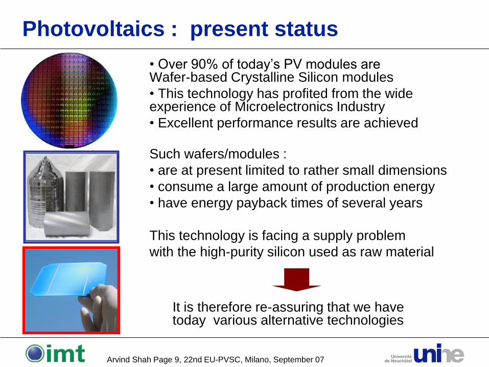
• Over 90% of today’s PV modules are Wafer-based Crystalline Silicon modules
• This technology has profited from the wide experience of Microelectronics Industry
• Excellent performance results are achieved
Such wafers/modules :
• are at present limited to rather small dimensions
• consume a large amount of production energy
• have energy payback times of several years
This technology is facing a supply problem
with the high-purity silicon used as raw material
Photovoltaics : present status
It is therefore re-assuring that we have today various alternative technologies
Arvind Shah Page 10, 22nd EU-PVSC, Milano, September 07
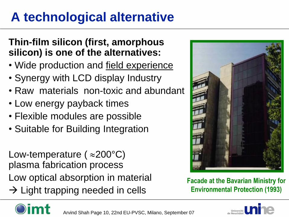
Thin-film silicon (first, amorphous silicon) is one of the alternatives:
• Wide production and field experience
• Synergy with LCD display Industry
• Raw materials non-toxic and abundant
• Low energy payback times
• Flexible modules are possible
• Suitable for Building Integration
Low-temperature ( 200°C) plasma fabrication process
Low optical absorption in material
Light trapping needed in cells
A technological alternative
Facade at the Bavarian Ministry for
Environmental Protection (1993)
Arvind Shah Page 11, 22nd EU-PVSC, Milano, September 07
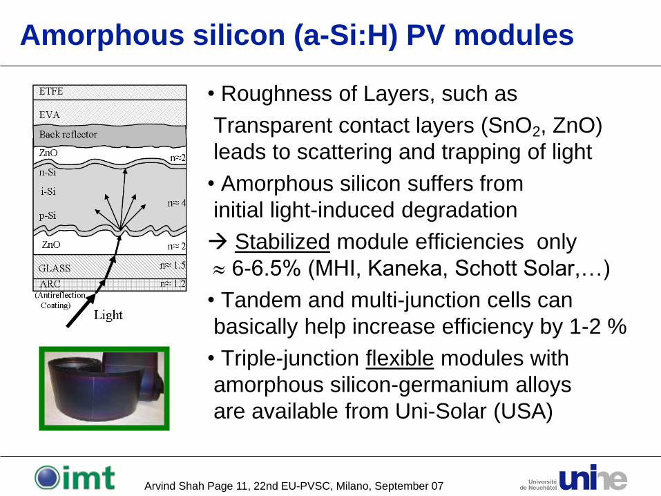
Amorphous silicon (a-Si:H) PV modules
• Roughness of Layers, such as
Transparent contact layers (SnO2, ZnO)
leads to scattering and trapping of light
• Amorphous silicon suffers from
initial light-induced degradation
Stabilized module efficiencies only
6-6.5% (MHI, Kaneka, Schott Solar,…)
• Tandem and multi-junction cells can
basically help increase efficiency by 1-2 %
• Triple-junction flexible modules with
amorphous silicon-germanium alloys
are available from Uni-Solar (USA)

Arvind Shah Page 12, 22nd EU-PVSC, Milano, September 07
Very-High frequency plasma enhanced CVD
• In 1985 we started our laboratory for amorphous
silicon solar cells at IMT Neuchâtel.
• We had not enough funds to purchase commercial
deposition equipment with the standard 13.56 MHz
plasma excitation frequency. We had to build the
deposition reactors ourselves. We therefore chose
80 MHz as plasma excitation frequency.
• This was the beginning of the Very High Frequency
(VHF) Plasma Deposition Technique (Freq > 25 MHz)
• VHF allows one to increase deposition rates
and obtain up to 3 x higher fabrication throughputs.
This means considerable savings in investment costs
• VHF is at present used by many Industries involved
in the production of amorphous silicon modules

Arvind Shah Page 13, 22nd EU-PVSC, Milano, September 07
With VHF Plasma Deposition it became
« easy » to produce high-quality hydrogenated
microcrystalline silicon (c-Si:H)
In 1995 IMT made the first microcrystalline
cells with over 5% efficiency
• they have (almost) no light-ind. degrad.
• they absorb near-Infrared light (gap 1.1 eV)
Since then, many other labs have also started
to study microcrystalline silicon
This form of thin-film silicon is complementary
to amorphous silicon (gap 1.75 eV)
Introduction of microcrystalline silicon (c-Si:H)
Microstructure of p-i-n c-Si:H solar cell
Microcryst. Si is very
complex: crystallites +
amorphous phase +
« cracks » !
! !
Arvind Shah Page 14, 22nd EU-PVSC, Milano, September 07
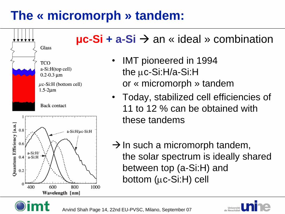
• IMT pioneered in 1994
the c-Si:H/a-Si:H
or « micromorph » tandem
• Today, stabilized cell efficiencies of
11 to 12 % can be obtained with
these tandems
In such a micromorph tandem,
the solar spectrum is ideally shared
between top (a-Si:H) and
bottom (c-Si:H) cell
The « micromorph » tandem:
μc-Si + a-Si an « ideal » combination

Arvind Shah Page 15, 22nd EU-PVSC, Milano, September 07
Maximum efficiency plot for tandem cells Conditions : all photons above Eg absorbed Voc & FF a/c to semi-empirical limits
but we are today (11.7% stabilized eff.)
still very far from upper limit (>30%)
Energy gaps Eg of µc-
Si:H and a-Si:H form an
almost ideal combination
Upper efficiency limit for
micro-morph tandem cell:
η > 30 % [A. Shah et al, J. of Non-Cryst. Solids,
Vol 338-340C, pp 639-645.]
μc-Si + a-Si an « ideal » combination ?
WHY?

Arvind Shah Page 16, 22nd EU-PVSC, Milano, September 07
Maximum short-circuit current density Jsc,
as a function of the gap Eg, for AM1.5
The « micromorph » tandem: μc-Si + a-Si
µc-Si
At present far too low
Jsc ≈ 23-25 mA/cm2
instead of 44 mA/cm2
Solution: light trapping
a-Si
Individual cell (almost) OK
within Tandem : Problem !
(light trapping more difficult here)
Solution: Intermediate Reflector
between top and bottom cell
limitations in current Jsc
0
10
20
30
40
50
60
70
0.5 1 1.5 2 2.5
Sh
ort
-cir
cu
it c
urr
en
t J
sc [
mA
/cm
2]
CIS c-Si
InP
Band gap energy Eg [eV]
GaAs
CdTe
a-Si
▲ ▼ : Experimental values
▼ ▲
c-Si

Arvind Shah Page 17, 22nd EU-PVSC, Milano, September 07
Semi-theoretical limit for Voc as a
function of gap Eg, for AM 1.5
illumination, calculated a/c to the diode
equation with Jo=1.5x10⁵ A/cm2 x
exp(-Eg/kT)) reverse saturation current
µc-Si
(500-600 mV : almost OK)
a-Si
Far below limit value
{0.9 V instead of 1.4 V}
Reason: EF cannot be pushed
by doping near to EC/EV,
due to amorphous structure
(Bandtails)
No known way out !
▼
µc-Si
▲
a-Si
▼▲experimental
values
limitations in voltage Voc
The « micromorph » tandem: μc-Si + a-Si

Arvind Shah Page 18, 22nd EU-PVSC, Milano, September 07
The « micromorph » μc-Si + a-Si tandem:
lab cells ↔ theoretical limits
equation Lab cell
Limit
Value
Jsc min{Jtop , Jbottom}
23/2 = 11.5
[mA/cm2]
20
[mA/cm2]
Voc Vtop + Vbottom
0.9 + 0.5
= 1.4 Volt
1.4 + 0.6
= 2.1 V
FF Average{FFtop, FFbottom} Aver{65%,75%} = 70%
76%
η 11.5 % 32 %
Arvind Shah Page 19, 22nd EU-PVSC, Milano, September 07
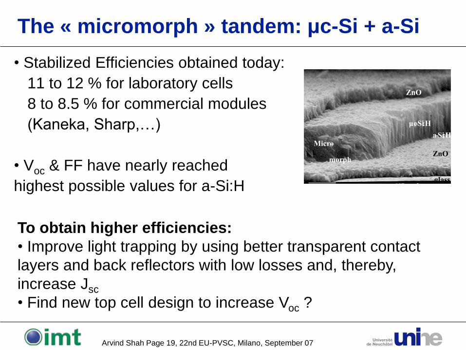
• Stabilized Efficiencies obtained today:
11 to 12 % for laboratory cells
8 to 8.5 % for commercial modules
(Kaneka, Sharp,…)
• Voc & FF have nearly reached
highest possible values for a-Si:H
ZnO
µc - Si :H
a - Si :H
ZnO
glass
Micro -
morph
The « micromorph » tandem: μc-Si + a-Si
To obtain higher efficiencies:
• Improve light trapping by using better transparent contact
layers and back reflectors with low losses and, thereby,
increase Jsc
• Find new top cell design to increase Voc ?

Arvind Shah Page 20, 22nd EU-PVSC, Milano, September 07
Micromorph Production equipment
Several industries offer production
equipment, originally designed for
Liquid Crystal Display Production:
• OERLIKON successfully uses the KAI
1200, for simultaneous Plasma
deposition of amorphous modules
on twenty glass panels of 1.4 m2 size;
Deposition of micromorph modules
is under development
• Applied Materials is currently
developing plasma deposition for
micromorph solar modules on 5.7m2
glass panels

Arvind Shah Page 21, 22nd EU-PVSC, Milano, September 07
Outlook
Thin-film silicon is economically and ecologically one of the
most promising materials for future large-scale photovoltaics
Low efficiencies are at present a limiting factor for a-Si based
modules, with typical values of of stabilized module
efficiencies of 6 to 8 % ( commercially available),
With microcrystalline/amorphous (« micromorph ») tandem
modules, one should be able to increase commercial
efficiency to 10 % , in the next 2 to 3 years
Key equipment suppliers are entering the market,
GWatts of production capacities announced by 2010
Goal (2010-2012) are modules at a production cost < 1€/Wp,
with an output power of 100 Wp/m2 and
an annual output energy (in Milano) of 100 kWh/m2

Arvind Shah Page 22, 22nd EU-PVSC, Milano, September 07
Acknowledgements and Thanks
The work at IMT’s PV Lab was financially supported by
the Swiss Federal Government
• Office féderal de l’énergie
• Commission for Technology and Innovation (CTI)
the European Commission
IMT’s Industrial Partners, especially:
IMT benefitted from close collaboration with many other
groups:
Prague, Jülich, Konstanz, Polytechnique Paris,
Princeton, AIST, …
Arvind Shah Page 23, 22nd EU-PVSC, Milano, September 07
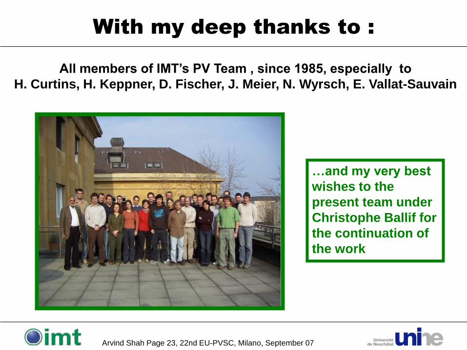
With my deep thanks to :
All members of IMT’s PV Team , since 1985, especially to
H. Curtins, H. Keppner, D. Fischer, J. Meier, N. Wyrsch, E. Vallat-Sauvain
…and my very best
wishes to the
present team under
Christophe Ballif for
the continuation of
the work

Arvind Shah Page 24, 22nd EU-PVSC, Milano, September 07
Thanks for your attention
Mont-Blanc and
University of
Neuchâtel at dawn
www.unine.ch/pv