theoretical foundations for joint digital-optical analysis of
TRANSCRIPT
Theoretical foundations for joint digital-optical
analysis of electro-optical imaging systems
David G. Stork and M. Dirk Robinson
Ricoh Innovations, 2882 Sand Hill Rd, Suite 115
Menlo Park, CA 94025-7054, USA
{stork,dirkr}@rii.ricoh.com
We describe the mathematical and conceptual foundations for a novel
methodology for jointly optimizing the design and analysis of the optics, de-
tector, and digital image processing for imaging systems. Our methodology is
based on the end-to-end merit function of predicted average pixel sum-squared
error to find the optical and image-processing parameters that minimize this
merit function. Our approach offers several advantages over the traditional
principles of optical design such as improved imaging performance, expanded
operating capabilities, and improved as-built performance. c© 2008 Optical
Society of America
OCIS codes: (110.0110) Imaging Systems, (100.6640) Superresolution
1. Introduction
An ever increasing portion of optical images are sensed by digital sensors and displayed
on digital devices. For instance, CCD-based digital cameras and computer screens continue
to supplant traditional silver-halide-based cameras and photographic prints. In this newer
technological environment, digital image processing in the data path can be used to process
1

the image before it is seen by users. Indeed, users rarely see traditionally projected opti-
cal images directly anymore as they did with film cameras. Optical system designers might
respond to this newer environment by designing ever more powerful image-processing algo-
rithms to correct the optical defects that inevitably remain in optical designs. Alternatively,
designers might recognize that this new environment offers a more radical, and, as we shall
demonstrate, far more powerful, design methodology.
We describe the mathematical and conceptual foundations for this novel methodology,
one that optimizes the joint design of the optics, detector, and digital image processing for
imaging systems. Our methodology is based on the end-to-end merit function of predicted
average pixel sum-squared error using linear models of the components as well as on Wiener
theory to find the optical and image processing parameters that minimize this merit func-
tion. Our methodology relaxes the traditional strict goal of traditional optical design that
the intermediate optical image be of high quality (e.g., small point-spread function). Im-
age processing compensates for the resulting optical degradations in an optimal way: some
optical aberrations are easier to correct through image processing than are others and our
optimization automatically adjusts both optical and image processing parameters to find the
best joint design. Although the intermediate optical image could be quite “poor” in systems
designed by our novel joint methods, the final, processed digital image is of higher quality
than images produced by systems designed by traditional sequential methods.
Traditional, sequential, techniques for designing optical imaging systems involves two
stages: first, the optical subsystem is designed to produce the highest quality optical im-
age, and second, the image processing is then designed to correct remaining defects in that
image. In contrast, we propose a method in which both the optics and the image process-
ing are jointly adjusted simultaneously for global system optimization (Fig. 1). Much of
the broad concepts of such end-to-end optimization are described in [1] which describe the
treatment of an imaging system as an information channel. Our current work explores the
application of this broad concept as it relates to the design of optical lens systems. Whereas
2

the original study of [1] considered simple parametric models describing the optical sub-
system, we describe how to employ commercial ray tracing software to provide physically
realistic models for the optical system.
A key element in the joint design approach is developing a unified framework for evalu-
ating the end-to-end performance of an imaging system. We model the source (scene) and
components, and then perform global optimization on the full optical, sensor, and image
processing parameters in order to extremize a performance criterion, subject to some costs.
Again, a key aspect of this approach is that the full electro-optical (digital-optical) system
is optimized; there is no need for either the optical system to appear optimal according to
standard optical measures of quality.
Recent approaches called wavefront coding pioneered by CDM Optics explore coopera-
tive interaction between the optical and digital subsystems [2–5]. Our method differs from
their wavefront coding technique which inserts non-standard lens surfaces or phase plates
into optical systems to achieve extended depth-of-field imaging. While the wavefront coding
technique exploits the cooperative interaction of optics and image processing, that research
primarily addresses the design or optimization of these non-standard surface components.
While the application of such wavefront coding techniques offers many of the same benefits in
terms of increased light levels and improved manufacturing tolerances, often the addition of
such non-standard surfaces increases the complexity and cost of manufacturing considerably.
Our approach expands on those ideas to include traditional lens surfaces. We stress that our
method is widely applicable even when extended depth-of-field is not of primary concern.
For example, our end-to-end optimization techniques produces higher image quality under
a fixed design budget for fixed distance finite conjugate imaging systems such as document
scanners using only traditional spherical lens surfaces.
The paper is organized as follows. In Sec. 2 we describe the complete imaging model
including the object or scene, optical subsystem, detector, and digital processing. In Sec. 3
we describe how we use this model to build digital-optical figures of merit. In Sec. 4 we
3

explore some of the advantages of using this design approach for an example design problem.
Finally, in Sec. 6 we present some insights into why this approach makes sense and conclude
with some future research directions.
2. System model
Traditionally, an imaging system seeks to reproduce an object under observation with as high
a fidelity as possible. The design process consists of changing design parameters to maximize
the fidelity, i.e., minimize the difference between an ideal image and an image produced by
the designed imaging system.
The first step in designing any imaging system is characterizing what an ideal image. In
our approach, the idealized image of a source object sobj(z) at a particular wavelength λ0 is
defined as
sideal(k) = [BT (x) ∗ P (sobj(z, λ))]∣∣∣k=Tx,λ=λ0
= [BT (x) ∗ sproj(x, λ)]∣∣∣k=Tx,λ=λ0
= [simg(x, λ)]∣∣∣k=Tx,λ=λ0
(1)
where P (·) represents the ideal projective (pinhole) transformation into the image coordinate
space x followed by an ideal bandpass filter with cutoff frequency matched to the spatial
sampling period T . Here k represents the indices of the pixel locations of the final sampled
image. Because our goal is for the imaging system to reproduce the idealized representation
of the image, we formulate the effects of the imaging system components in terms of this
idealized image sideal(k). As such, we make use of the distinction between the function s
in the three-dimensional object space sobj, after being projected onto the image plane sproj,
after passing through some idealized optics simg and after sampling sideal.
4

2.A. Source model
In most applications, the space of all possible objects to be imaged is naturally constrained by
the intended task or range of application settings, for instance, it would be highly constrained
in the case of a bar code readers but quite unconstrained for general purpose consumer
cameras. Be it large or small, the boundedness of this image space offers important prior
information for the imaging system designer.
In this paper, we assume that we know the power spectrum of the object signal in terms of
image coordinates x. While in some cases we can derive such information from first principles,
here we estimate the power spectrum (PSD) from a collection of representative training
images. In our experiments for a document scanner, we restrict our class of signals to those
which are grayscale images of 300 dpi documents. We estimate the statistical distribution of
the source signal from a randomly selected collection of portions from a collection of 300 dpi
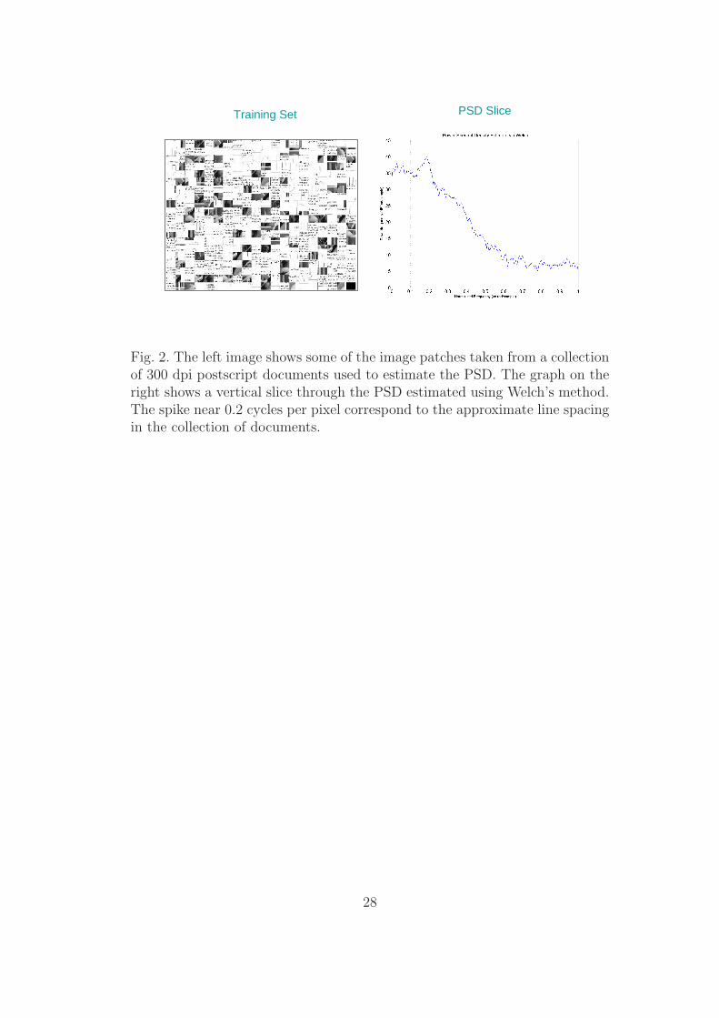
postscript files. The left image of Fig. 2 shows some of the samples tiles used to estimate the
PSD for grayscale documents. The image on the right shows a slice through the vertical axis
of the PSD estimated using Welch’s method (or periodogram method) in which the signal
is broken into equal-sized blocks and the power spectrum estimated within each block [6].
The PSD slice shows a spike near 0.2 cycles per pixel corresponding to the approximate
line spacing in the collection of documents. Such a component suggests the importance of
preserving information at this spatial frequency range. We will use this PSD example later
in our simulations.
2.B. Optics model
The optical lens systems, having a focal length f , are comprised of spherical lens elements
projecting a real inverted image onto a planar digital sensor, such as a CCD array. The
optics of the imaging system affects this two-dimensional luminance function according to
5

the spatially-varying convolution integral
∫s(x− x)hopt(x, x)dx, (2)
where h(x, x) is the optical system’s spatially-varying point spread function (PSF). The x
represents the convolution slack variables.
Every lens system’s point spread function depends on the geometric aberrations. The point
spread function is related via the wavefront distortion measure known as the Optical Path
Difference or OPD function OPD(p,x) where p represents the two-dimensional coordinates
in the exit pupil plane of the optical system and x represents the image coordinates. In an
ideal imaging system, the wavefront (surface of equal phase) at the exit pupil of the lens
system would have a perfect spherical shape whose center is in the image focal plane. This is
the ideal reference sphere and geometric rays associated with such an ideal wavefront would
converge to a single point. Geometric aberrations correspond to a departure or OPD of the
actual wavefront from this ideal reference sphere.
The optical system’s PSF at a particular field location x is a function of the OPD according
to
hopt(x, x) ≈∣∣∣∣∫
A(p)ejOPD(p,x)ej2πxpdp
∣∣∣∣2
, (3)
where OPD(p,x) is expressed in terms of the exit pupil coordinates p and the image location
coordinate x. The function A(p) is the magnitude of the exit pupil (most commonly either 0
or 1). This function is based on the magnitude of the inverse Fourier transform of the pupil
function, A(p)ejOPD(p,x) [7].
We note that the OPD function is very often the primary means by which optical lens
designers evaluate and optimize lens systems. For example, the OPD function can be ex-
pressed as a linear combination of polynomial functions in p and x. Optical systems have
been evaluated based on the five 3rd-order polynomials corresponding to the Seidel aber-
rations (distortion, astigmatism, coma, field curvature, and spherical aberration). The lens
6

designer attempted to balance these aberrations to meet the imaging specifications. The most
common traditional optical figure of merit used when optimizing lens designs involves some
form of the square of the OPD function averaged over the lens exit pupil, i.e., OPD-RMS or
geometric spot size [8, 9].
2.C. Detector Model
The detector transduces light into digital information, represented in bits. The projected
image, sproj(x, λ), is then filtered by an ideal bandpass filter matched to the spatial sam-
pling period T . In principle, the bandpass filter should prevent aliasing while maintaining
all the spectral information of the image within the sampling bandwidth. Such an ideal
bandpass filter, however, is physically unrealizable. In many imaging sensor devices, such
as charge coupled devices, CCDs, the area of the detector associated with an individual
pixel corresponds to a rectangular aperture whose dimensions are a percentage of the over-
all pixel size; the percentage of the pixel spacing which captures photons is known as the
fill factor. Detectors with larger fill factors offer the advantage of capturing more light as
well as eliminating aliased image content. For rectangular pixel apertures, the pixel transfer
function is given by Hpix(ω) = sinc(ff2
ω1)sinc(ff2
ω2) where ff is the fill-factor and ω rep-
resents the two-dimensional normalized spatial frequency coordinates (range from [-1,1]). In
our experiments, we assume square pixels.
We combine the optical PSF and the pixel PSF to obtain a system PSF, i.e., htot(x, x) =
hopt(x, x) ∗ hpix(x). We express the imaging system using vector notation where the ideal
sampled image is denoted s and the sampled point spread function is denoted H, whose
elements are given by
[H]jk = htot(x = Tj, x = Tk). (4)
Random noise often arises as photons are transduced to electrons and quantized in bits in
an imaging system. We make two assumptions in modelling such detector noise. First, we
assume that enough photons are captured by the detector so that other noise (thermal, dark
7

current, etc.) is negligible compared to the photon or shot noise. Second, we approximate
the Poisson noise as additive Gaussian noise with variance σ2, whose value depends upon
the corresponding gray scale value. Below, when designing image processing filters, we make
the simplifying assumption that the noise power is not spatially dependent on the signal
s, but instead depends on the overall signal power as reflected by the average number of
photons per pixel. We use the full signal-dependent noise model, however, when simulating
the imaging path.
From Sects. 2.A–2.C, we see that the following linear model represents the entire imaging
process
y = Hs + n, (5)
where H is the total system point spread function operator and n represents the random
noise associated with the imaging system.
2.D. Image processing model
In the present work, we restrict image processing models to linear processing. Such filtering
enables analysis in the dual, spatial-frequency domain, specifically through the use of Fourier
transforms. Our general method can exploit other, non-linear, image processing as well,
though typically at the expense of added complexity.
We assume that our image processing system applies a spatially-varying filter r(k) to the
captured digital image y. As with Eq. 5, we represent the image filter in matrix form as
R. This filter is designed so as to minimize the mean-square error (MSE) between the ideal
image s and the filtered image Ry, that is,
mincEn,s
[‖Ry − s‖2], (6)
where the subscript on the expectation operator E represents that the expectation is taken
over the random noise n and the (assumed) stationary random signal s.
In our simulations, we approximate the full spatial variability by a number of separate
8

filters, each spatially-invariant within an image block. Thus, within a such a block, the
MMSE filter (the Wiener filter) can be expressed in the Fourier domain as
R(ω) =H∗
tot(ω)Ps(ω)
|Htot(ω)|2Ps(ω) + σ2, (7)
where Ps(ω) represents the power spectrum of the source model introduced in Sect 2.A.
The filter spectrum of Eq. 7 is ideal in the MSE sense. In practice, achieving this spectral
response may be difficult or impossible due to constraints on the image processing hardware
such as filter geometry or coefficient constraints. Figure 3 shows some examples of constrained
filter geometries typically encountered in real image processing subsystems. Such constrained
digital filters may be designed using in a MSE-optimal fashion as taught in [10, 11]. When
using constrained digital filters, the spectral response will not, however, match the ideal
Wiener filter response of Eq. 7.
3. Information-based optimization
Design involves adjusting the design parameters Θ to extremize a figure of merit. Optical
design parameters, Θo, include such properties and the lens radii, thickness, air spacings,
and glass types. Digital design parameters, Θd, include the filter sizes, filter coefficients, bit
depth, and thresholding parameters.
The traditional approach to designing electro-optical imaging systems involves first opti-
mizing the lens system over the optical design parameters Θo. The optical engineer takes a
collection of design specifications and uses commercial lens design software to try and sat-
isfies the design constraints while maximizing optical performance. The traditional optical
performance figure of merit is based on geometric spot size or wavefront error (such as OPD-
RMS). To find such a design, the optical engineer combines heuristic knowledge of lens design
and powerful optimization capabilities included in lens design software packages. Once this
design process is complete, the optical systems are built and tested. Some time later, digital
processing engineers design the image processing for the imaging system. For our purposes,
9

we assume that these image processing parameters Θd are optimized to minimize some form
of MSE. As we shall show, this traditional sequential approach leads to design inefficiencies
and ultimately inferior performance.
As mentioned, in our approach we jointly optimize both the optical and digital design
parameters using the final image processing MSE error metric as a digital-optical figure of
merit. In this way, we explore the joint optical and digital design space to find more efficient
designs [11,12]. To achieve this, we must predict the MSE performance for the entire electro-
optical imaging system. For a filter having a spectral response R(ω), the MSE is predicted
by
MSE(Θ) =
∫Ps(ω)|Htot(ω,Θo)R(ω,Θd)− 1|2 + |R(ω,Θd)|2σ2dω, (8)
where Ps(ω) is the PSD for the signal class and σ2 is the noise power for the system [10]. In
this way, we see that the end-to-end MSE performance is a function of both the optical and
the digital design parameters and the signal statistics.
Computing the predicted MSE using Eq. 8 requires that we first design the filter and
compute the filter response R(ω,Θd). If we assume that we can achieve the ideal Wiener
filter response defined in Eq. 7, the predicted MSE for a particular field angle reduces to
MSE(Θ) =
∫Ps(ω)σ2
|Htot(ω,Θo)|2Ps(ω) + σ2dω. (9)
Equation 9 shows that the predicted MSE is a function of the optical design parameters Θo
via the system transfer function Htot(ω). The digital design parameters are defined implicitly
to be those that produce a filter with the frequency response given by Eq. 7.
To achieve this joint digital-optical design optimization, we leveraged the optimization
capabilities of the commercial lens design software Zemax [13]. Zemax includes powerful op-
timization capabilities specially tuned for optical design. The software also has the capability
of optimizing optical designs based on user-defined optimization criterion (UDOP). Figure
10

4 shows a general block diagram of the software architecture for the joint compensation
strategy. In this we, we are able to exploit the ray tracing and optimization capabilities
of Zemax while performing digital-optical design. Using Zemax to drive the entire design
process also allows the design to incorporate traditional optical design constraints such as
element spacings, glass types, curvatures, etc. Zemax also provides convenient tools for sim-
ulating standard manufacturing errors in a Monte Carlo (MC) type analysis for predicting
image system yields.
4. Design Examples
In this section, we explore some electro-optical design examples highlighting some of the
advantages of the joint digital-optical design methodology. All of our examples are based on
the general imaging specifications for a linear document scanning system.
The general specifications for the document scanner imaging system are shown in Table
1. The table shows that the optical system is a f = 72 mm imaging system operating at a
finite conjugate working distance of 500 mm with a field of view of approximately ±15◦.
In out design examples, we show the resulting captured and processed images after passing
through a simulated version of the imaging system. We simulated the entire end-to-end
imaging performance using a software image formation model similar to that described in [14]
except that here we used a one-dimensional linear array rather than a two-dimensional focal
plane array. The method of [14] simulates the effects of the optical system on the input
image in three steps. First, the relative illumination over the field of view is extracted from
the lens design software to compute a gain function which tends to darken the image at the
edge of the field. Second, the optical distortion map, extracted from Zemax, is applied to the
input image using cubic spline interpolation for each of the three wavelengths independently.
Third, the point-spread function is applied to the distorted image in tiles to capture the
spatially-varying natures of the PSF. Similar to the forward imaging simulation process,
we separate the image processing into two steps. First, we restore image contrast using the
11

Wiener sharpening filters. Second, we correct the distortion and illumination errors.
When simulating the optical system, we divide the full image field into 20 equally-spaced
field angles to capture the spatially-varying nature of the optical system. Within each of
these field angles we use Zemax to compute the sampled point spread function (PSF) and
apply this PSF to all the pixels in this region assuming local spatial invariance within the
tile. For simulation purpose, when simulating the noise in the system, we include both an
additive sensor read noise as well as a signal-dependent shot noise. Thus, even though our
image processing models are based on additive noise models, we experiment using signal-
dependent noise models when simulating performance. For all of our examples, we use a
grayscale text document source image sampled at 300 dpi.
There are two ways to calculate the system performance through simulation:
• Compute the error in the final system as the average pixel-wise square error (MSE)
between the processed image s(x) and the ideal noise free image s(x).
• Compute the performance as the average pixel-wise square (MSE) error between the
distorted ideal image and the sharpened image prior to distortion correction.
The problem with the first experimental performance measure is that slight distortion mis-
registrations between the processed image and the ideal image would yield very poor perfor-
mance even if the contrast properties of the images were otherwise ideal. Measuring perfor-
mance the second way assures that the RMSE performance reflects the contrast and SNR of
the final image. The motivating rationale is that minor distortion artifacts are less visually
objectionable than contrast loss.
4.A. Focussing a Singlet Lens
In this section, we show a very simple example motivating the joint digital-optical design
approach. In this example, we start with a simple rear meniscus lens. The singlet lens has
the aperture stop 11 mm in front of the singlet. The 10mm thick BK7 singlet is bent towards
the object. The front surface has a radius of curvature of -74 mm and a back surface a radius
12
of curvature of -26 mm. In this design, we evaluate using a single wavelength of λ = 550 nm.
The optical system is a relatively slow F#8.0 system.
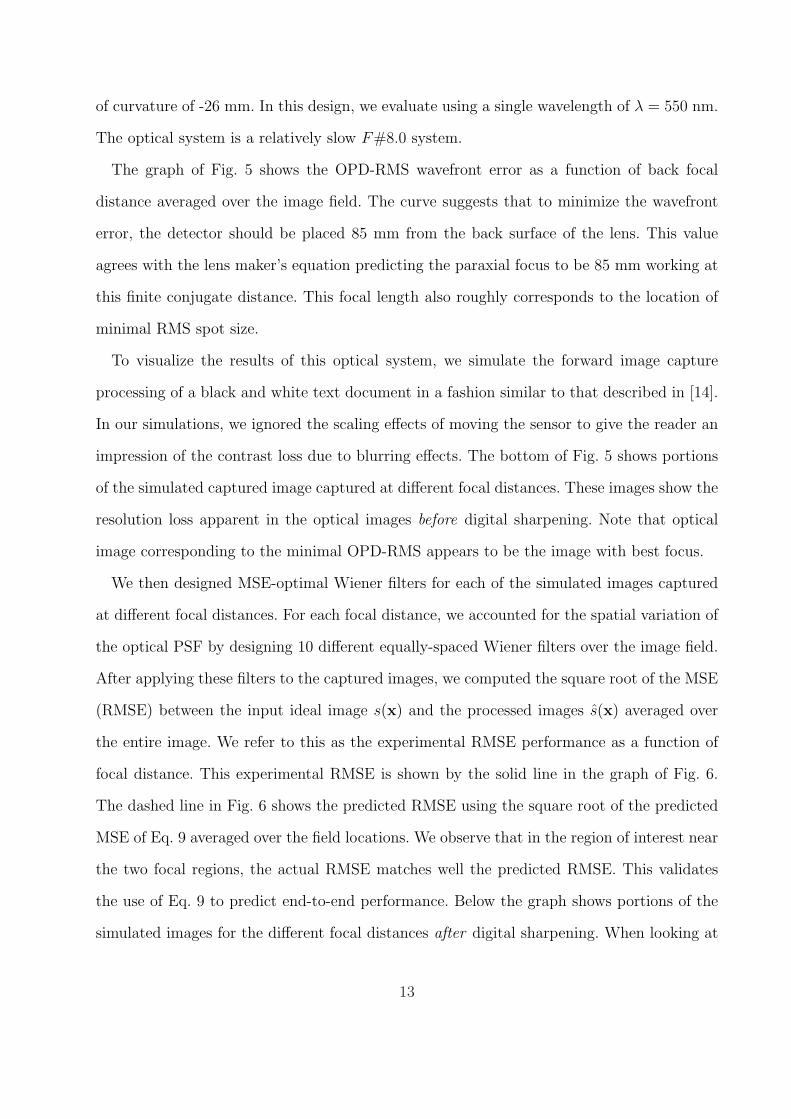
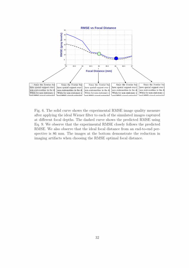
The graph of Fig. 5 shows the OPD-RMS wavefront error as a function of back focal
distance averaged over the image field. The curve suggests that to minimize the wavefront
error, the detector should be placed 85 mm from the back surface of the lens. This value
agrees with the lens maker’s equation predicting the paraxial focus to be 85 mm working at
this finite conjugate distance. This focal length also roughly corresponds to the location of
minimal RMS spot size.
To visualize the results of this optical system, we simulate the forward image capture
processing of a black and white text document in a fashion similar to that described in [14].
In our simulations, we ignored the scaling effects of moving the sensor to give the reader an
impression of the contrast loss due to blurring effects. The bottom of Fig. 5 shows portions
of the simulated captured image captured at different focal distances. These images show the
resolution loss apparent in the optical images before digital sharpening. Note that optical
image corresponding to the minimal OPD-RMS appears to be the image with best focus.
We then designed MSE-optimal Wiener filters for each of the simulated images captured
at different focal distances. For each focal distance, we accounted for the spatial variation of
the optical PSF by designing 10 different equally-spaced Wiener filters over the image field.
After applying these filters to the captured images, we computed the square root of the MSE
(RMSE) between the input ideal image s(x) and the processed images s(x) averaged over
the entire image. We refer to this as the experimental RMSE performance as a function of
focal distance. This experimental RMSE is shown by the solid line in the graph of Fig. 6.
The dashed line in Fig. 6 shows the predicted RMSE using the square root of the predicted
MSE of Eq. 9 averaged over the field locations. We observe that in the region of interest near
the two focal regions, the actual RMSE matches well the predicted RMSE. This validates
the use of Eq. 9 to predict end-to-end performance. Below the graph shows portions of the
simulated images for the different focal distances after digital sharpening. When looking at
13

the processed images, we observe that the ideal back focal distance appears to be closer to
86 mm, nearly a full millimeter behind the OPD-RMS optimal focal plane. Furthermore,
the region around this MSE-optimal focal distance also performs much better than the best
OPD-RMS focal distance. In fact, even out to 87 mm, the RMSE performance is better than
the traditional focal distance of 85 mm even though the OPD-RMS is nearly 3X worse.
In this experiment we observe that the predicted RMSE of Eq. 9 offers reasonable predic-
tion of the end-to-end performance of the complete imaging system. More importantly, the
experiment demonstrates that traditional wavefront error metrics are an unreliable guide to
the end-to-end electro-optical performance in even the simplest decision of how to focus a
lens.
4.B. Triplet Lens Design
In the previous section, we demonstrated the shortcomings of the traditional sequential
approach to evaluating electro-optical imaging systems. In this section, we examine a more
realistic design form for a document scanner; namely, a triplet lens system. In this case, we
compare the performance of a traditionally design triplet lens system and the joint optical-
digital design. Table 2 shows some of the design constraints on the triplet lens system.
The triplet optical system has twelve design parameters which include the six surface
curvatures, the three lens thicknesses, two air spacings, and the back focal distance. The
digital sharpening system is constrained to 10 K × K square filters over the image field
for each of the three color bands (RGB). We explored filter geometries ranging from 9 × 9
taps to 27 × 27 taps. We designed the scanner lens plus digital subsystems under the same
system constraints using three different design approaches. We experimentally compute the
RMSE performance using the simulation approach described earlier for the sets of design
parameters Θ for each of the different design strategies.
Traditional OPD-RMS Design We followed the traditional sequential design path of
initially designing the lens system using standard OPD-RMS figure of merit. The merit
14

function was constructed using four field angles out to the maximum field height.
We used global optimization within Zemax to find the best OPD-RMS design which
satisfied the optical constraints. As a subsequent step, we design the MSE-optimal
K ×K filters for ten different field locations.
Optimistic MSE Design We optimized the imaging system in a joint fashion using the
fast but optimistic MSE prediction UDOP based on Eq. 9. In this case, the MSE is
computed without incorporating the digital filter geometric constraints. We used the
traditional OPD-RMS minimized lens as the initial starting point used the damped
least-square optimization routine of Zemax. After this fast joint optimization, the set
of MSE-optimal K ×K filters were optimistic MSE lens design.
Filter-specific MSE Design We optimize the both the lens system and the digital filters
jointly based on the filter size by designing the MSE-optimal filters for each step
and computing the predicted MSE using Eq. 8. In this approach, we performed a
separate optimization process for each value of K producing a different lens design as
a function of filter size. We used the optimistic MSE based design produced by the
second approach as an initial guess for the damped least squares optimization.
Figure 7 compares the experimental RMSE performance of the three different design strate-
gies as a function of filter size K. We see that the optimistic MSE design produces about a
10 percent improvement in performance over the traditional sequential approach. Also, we
see that increasing the filter size improves performance as we would expect. The solid line
indicates the performance of geometry-specific MSE designs, each optimized for a different
filter size. These systems offer an additional 10 percent improvement in performance while
almost matching the optimistic RMSE performance bound predicted by Eq. 9 shown as the
dash-dot straight line. This suggests, that for a particular set of filter size constraints a unique
lens design can be matched to maximize performance. The gap between the dashed line (op-
timistic MSE) and this bound shows the performance loss when applying space-constrained
15
image processing filters to a lens which was optimized assuming unconstrained filters.
Optimizing a digital imaging system using the predicted MSE of Eq. 9 is much faster than
using the complete predicted MSE of Eq. 8 as the filters need not be explicitly designed
as a separate step. The results of Fig. 7 suggest designing imaging systems with space-
constrained filters could be more efficiently achieved using a two step process. First, the
system is optimized using a fast optimization routine based on the optimistic predicted MSE
followed by a slower optimization based on the complete MSE prediction of Eq. 8.
An unexpected result was that the MSE-optimal designs show inferior optical performance
with regards to the OPD-RMS. Fig. 8 compares the the polychromatic OPD-RMS as a
function of field location for the traditional OPD-RMS design and the joint digital-optical
design based on the optimistic MSE function. The OPD-RMS is slightly better than the
traditional design near the optical axis, but exhibits much worse OPD-RMS at large field
heights. This digital-optical lens design has an average polychromatic OPD-RMS of about
0.65 waves of error over the image field as opposed to only 0.5 waves of OPD-RMS error
over the image field for the traditional optical system. Both systems show performance
significantly worse than the diffraction limit due to the large field of view requirements.
To visualize the difference in performance we show small portions of the simulated images
for both the traditional and the optimistic joint digital-optical design in Fig. 9 towards the
edge of the field. The images in the left column show the captured and processed images for
the traditionally designed optical system. The captured optical image for the traditional sys-
tem shows some blurring but minimal lateral chromatic aberration and coma. The processed
image, however, shows the ringing characteristic of information loss due to zero-crossings in
the MTF. The images in the right column show the captured and processed images for the
jointly designed system. The captured images show significant coma and lateral chromatic
aberration as evidence by the vertical smearing of the image. It is these aberrations which
contribute to the inferior OPD-RMS shown in Fig. 8. After image processing, however, the
image shows high contrast with almost not visible artifacts. Thus, the aberrations which
16
were ignored in the joint design are easily corrected with digital processing.
5. Digital-optical Compensation
In this section we explore how to extend the digital-optical design philosophy to the realm
of manufacturing to improve as-built image system performance. All optical systems when
manufactured and assembled include random amounts of errors. Traditionally, when optical
lens systems are assembled there is some form of mechanical adjustment to compensate for
these errors. The compensation strategies are often based on wavefront error or a single MTF
value. Most often, the image processing subsystems is not considered during this mechan-
ical adjustment. In fact, most commercial imaging systems apply a fixed image processing
system regardless of the quality of the as-built optical system. Even in the most optimistic
cases, the adjustment of the digital processing subsystem occurs after fixing the mechanical
compensation parameters.
The sequential approach ignores the potential of image processing to compensate for the
shortcomings of the electro-optical system. In the previous sections we demonstrated the
value of designing electro-optical imaging systems from an end-to-end perspective. Now, we
show the improvements when applying this same methodology to compensation of as-built
systems. Instead of the traditional sequential approach to electro-optical compensation, we
propose jointly adjusting both the optical and the digital parameters during the assembly and
compensation of imaging systems. The joint compensation strategy is based on predicted end-
to-end MSE performance of Eqs. 9. We envision a test environment in which the optical test
engineer evaluates the optical system with knowledge of the electronic subsystem to which it
will be mated. Our experimental setup presumes that reasonably high quality estimates of the
as-built optical performance in terms of the OTF are available. Since the MSE performance
depends only on the OTF, we can also envision a test environment where compensation
occurs after combining the optical and electronic subsystems.
We perform a Monte Carlo (MC) simulation in which we compare the predicted RMSE
17

performance for a sequentially adjusted as-built system with a jointly adjusted system. We
use the tolerance analysis capabilities of Zemax to simulate the random errors associated
with optical manufacturing. The manufacturing errors for this lens include perturbations
on all six surface radii, element thicknesses, element centers, element tilts, surface tilts, and
surface centers. When generating a random as-built system, the perturbation values for each
of these errors come from zero-mean Gaussian distributions with standard deviation of 0.0125
µm in keeping with standard manufacturing tolerances. We use the traditionally designed
triplet of the previous section as the nominal design. In other words, we are evaluating the
joint compensation approach for a nominal design optimized using traditional techniques
(OPD-RMS).
Similar to the design portion of the paper, we compare the RMSE performance distribution
for randomly perturbed as-built systems having a mechanically adjustable back focal distance
to compensate for manufacturing errors. We compare the RMSE performance of the as-
built systems using two different methods for selecting the optimal back focus compensation
setting.
1. The traditional method is based on minimizing an OPD-RMS error metric measured
using wavefront measurement equipment such as an interferometer. After adjusting the
back focal distance of every as-built system to minimize the OPD-RMS, the system-
specific Wiener filter is applied to the system and the predicted RMSE is computed.
This parallels the traditional approach of sequential design.
2. The digital-optical method adjusts the back focal distance of each as-built system to
minimize the predicted RMSE metric directly based on an OTF measurement equip-
ment.
The CDF curves shown in Fig. 11 compare the final RMSE performance of using these two
different compensation strategies.
To compare the performance of the sequential and joint compensation strategies we use Ze-
18

max tolerancing scripts during the MC simulation. In the traditional compensation strategy,
we first perform twenty iterations of local optimization based on the OPD-RMS wavefront
error at 0%, 70%, and 100% field. Implementing this in practice would require some form of
interferometric or wavefront sensing test setup. Such a compensation simulation provides an
optimistic perspective of the as-built performance based on sequential compensation strat-
egy. After minimizing the OPD-RMS, we compute the ideal Wiener filter for the set of 10
equally-spaced field locations and predict the optimistic RMSE performance using Eq. 9.
This predicts the end-to-end performance after applying the ideal Wiener filter of Eq. 7 for
the fixed optical compensation parameters. To simulate the joint digital-optical compensa-
tion strategy, our Zemax compensation script performs five iterations of local search based
directly on the average optimistic predicted RMSE of Eq. 9 for the 10 field locations. While
such a compensation strategy presumes numerous MTF measurements have been made over
the image field, this could be done very efficiently using a full-field calibration test target
since wavefront estimation is unnecessary.
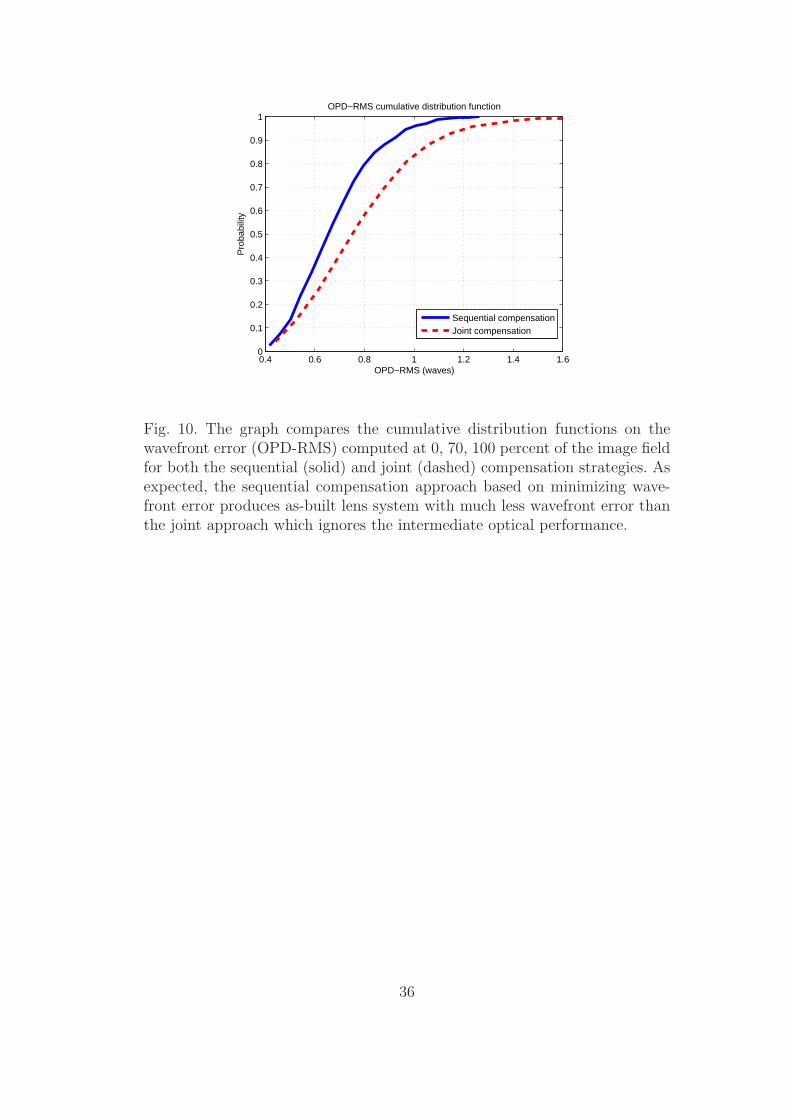
Figure 10 compares the cumulative distribution function (cdf) over the set of 1000 as-
built systems in terms of the OPD-RMS over the image field. We observe that the joint
approach (dashed line) to adjusting the imaging system produces optical subsystems with
poorer optical quality (in terms of OPD-RMS) than those adjusted using the OPD-RMS
(solid line). This is in keeping with our observation that the jointly designed or compensated
systems will often have inferior optical performance.
Figure 11 compares the predicted end-to-end RMSE performance distributions of the two
compensation approaches. Here we see a significant improvement in the predicted RMSE
performance of the as-built systems which were adjusted in a joint digital-optical fashion
(dashed line) over the sequentially adjusted systems (solid line). For example, almost twice
as many systems achieve 6.0 gray levels of RMSE error when using joint compensation as
opposed to sequential compensation.
19

6. Conclusions and future work
What is the source of the superiority of the joint design method over traditional sequential
methods? It is an engineering truism that just as the optimal transportation route from New
York to Boston is not the concatenation of the optimal route from New York to Chicago to the
optimal route from Chicago to Boston, so too the optimal information path from external
visual world to final displayed digital image need not be the optimal path from world to
projected optical image and the optimal from this optical image to displayed digital image.
The high-dimensional space of optical design parameters and digital filter design parameters,
is quite unlikely separable. Our joint method can explore designs that allow “low quality”
optical images that would never be explored through sequential design methods.
We can gain a bit more insight into the source of the benefit by considering the modulation
transfer functions (MTFs) due to “equivalent” severity among different optical aberrations.
Figure 12 shows the MTFs of a simple triplet optical system designed five ways, each allowing
the same OPD-RMS error, i.e., a roughly “equivalent” amount of such aberrations. Notice
that some of the MTFs have zeros, and others do not. No amount of linear digital filtering can
recover the information lost at such zeros. As such, some aberrations can be easily corrected
through digital filtering, others cannot.
Our investigations have generated several observations about the application of digital-
optical design. For instance, we observe that digital-optical design is most suited to chal-
lenging optical designs where traditional designs cannot meet the size, cost, or performance
specifications. Intuitively, as the number of lenses or glass qualities increase, the optical
system will approach diffraction-limited performance. In this case, digital-optical design (in
the context of standard optical surfaces) holds little advantage during design. But, as the
complexity of such systems increases, the likelihood that the as-built system will match the
nominal design decreases. In these cases, digital-optical compensation becomes very impor-
tant.
We have shown that a global approach to optical system design can yield superior designs
20

to the traditional sequential method. We believe that this underscores our conclusion that
information-based optimization of electro-optical systems will provide a benefit for simple
(and thus cheap) imaging systems. We intend to build a unified framework to understand
when leveraging image processing allows cost reduction or new capabilities of in joint design
space.
In the future, we will explore new methods for efficiently navigating the joint optical-digital
design space to speed up the joint optimization. Additionally, future work will explore specific
designs under novel nonlinear image processing and non-standard performance metrics.
References
1. C. Fales, F. Huck, and R. Samms, “Imaging system design for improved information
capacity,” Applied Optics 23, 872–888 (1984).
2. W. T. Cathey and E. Dowski, “A new paradigm for imaging systems,” Applied Optics
41, 6080–6092 (2002).
3. G. E. Johnson, A. K. Macon, and G. M. Rauker, “Computational imaging design tools
and methods,” in “Novel optical systems design and optimization VII: Proceedings of
SPIE,” , vol. 5524, J. M. Sasian, R. J. Koshel, P. K. Manhart, and R. C. Juergens, eds.
(SPIE Press, Bellingham, WA, 2004), vol. 5524.
4. R. Narayanswamy, G. Johnson, P. Silviera, and H. Wach, “Extending the imaging volume
for biometric irirs recognition,” Applied Optics 44, 701–712 (2005).
5. P. Silviera and R. Narayanswamy, “Signal-to-noise analysis of task-based imaging sys-
tems with defocus,” Applied Optics 45, 2924–2934 (2006).
6. P. D. Welch, “The use of fast Fourier transforms for the estimation of power spectra: A
method based on time averaging over short modified periodograms,” IEEE Transactions
on Audio and Electroacoustics 15, 70–73 (1967).
7. J. W. Goodman, Introduction to Fourier Optics (McGraw-Hill, New York, NY, 1986),
2nd ed.
21

8. R. E. Fischer and B. Tadic-Galeb, Optical System Design (McGraw-Hill, New York,
2000).
9. W. J. Smith, Modern Optical Engineering (McGraw-Hill, New York, NY, 2000).
10. A. K. Jain, Fundamentals of Digital Image Processing (Prentice Hall, Englewood Cliffs,
New Jersey, 1989), 1st ed.
11. M. D. Robinson and D. G. Stork, “Joint design of lens system and digital image process-
ing,” in “Proceedings of the International Optical Design Conference,” , vol. 6342,
G. Gregory, J. Howard, and J. Koshel, eds. (OSA, 2006), vol. 6342.
12. D. G. Stork and M. D. Robinson, “Information-based methods for optics/image process-
ing co-design,” in “Proceedings of the Fifth international workshop on information op-
tics,” , vol. 860, B. J. G. Cristobal and S. Vallmitjana, eds. (AIP Press, 2006), vol. 860,
pp. 125–35.
13. Z. D. Corporation, ZEMAX User’s Guide (San Diego, CA, 2004).
14. P. Maeda, P. B. Catrysse, and B. A. Wandell, “Integrating lens design with digital
camera simulation,” SPIEProceedings SPIE Electronic Imaging, San Jose, CA 5678,
48–58 (2005).
22

List of Figure and Table Captions
Fig. 1. Top: In the traditional electro-optical imaging system design methodology, the op-
tical subsystem and the image processing subsystem are designed and optimized se-
quentially. This method may give a possibly complex optical system and a high-quality
optical image. Bottom: A joint optimization method often produces a smaller but lower-
quality optical subsystem together with a more complex image processing subsystem,
yielding a final digital image that is of equal or better quality to that produced by the
system designed by traditional methods.
Fig. 2. The left image shows some of the image patches taken from a collection of 300 dpi
postscript documents used to estimate the PSD. The graph on the right shows a vertical
slice through the PSD estimated using Welch’s method. The spike near 0.2 cycles per
pixel correspond to the approximate line spacing in the collection of documents.
Fig. 3. The graphic shows some examples of geometrically constrained digital filters. These
digital filters vary in their computational complexity (function of the number of taps)
as well as their ability to approximate the ideal Wiener filter spectral response of Eq. 7.
Fig. 4. The figure outlines the general software components of joint digital-optical compen-
sation software. For each iteration of the optimization process, a function call is made
to the UDOP module which computes the predicted RMSE for the current state of
the optical design. During the computation of the predicted MSE, the UDOP software
uses the Zemax ray tracing capability to compute the needed wavefront error functions
used to compute Htot(ω).
Fig. 5. The top graph shows the wavefront error (OPD-RMS) as a function of the focal
distance. According to the effective focal length of the lens system, the detector should
be placed at a distance of 84.75mm from the lens. This corresponds to the focal point
minimizing the OPD-RMS wavefront error. Below the graph are portions of the simu-
23

lated captured image. We observe that the minimal OPD-RMS image appears to have
the sharpest resolution.
Fig. 6. The solid curve shows the experimental RMSE image quality measure after applying
the ideal Wiener filter to each of the simulated images captured at different focal
depths. The dashed curve shows the predicted RMSE using Eq. 9. We observe that
the experimental RMSE closely follows the predicted RMSE. We also observe that the
ideal focal distance from an end-to-end perspective is 86 mm. The images at the bottom
demonstrate the reduction in imaging artifacts when choosing the RMSE optimal focal
distance
Fig. 7. The graph compares the experimental RMSE performance for our test image using
the complete (optical + digital) imaging systems produced using three different design
approaches as a function of the digital filter size. The dotted line indicates the perfor-
mance of the traditional sequential image system design in which the lens system is
first designed to minimizes OPD-RMS wavefront error followed by subsequent design
of the image processing filters. The dashed line indicates the performance of the opti-
mistic MSE-based design where the lens was first designed using the optimistic MSE
prediction of 9 followed by subsequent design of geometry-constrained digital filters.
We see that this design produces about a 10 percent improvement in performance over
the traditional sequential approach. The solid line indicates the performance of multi-
ple imaging systems each optimized in a joint fashion while considering the geometry
constraints on the digital filter. These systems offer an additional 10 percent improve-
ment in performance while almost matching the experimental RMSE achieved when
applying the ideal Wiener filter.
Fig. 8. The graph compares the polychromatic OPD-RMS wavefront error over the field
of view for the lens system optimized based on OPD-RMS (solid) and based on the
optimistic MSE (dashed). The digital-optical design shows significantly worse optical
24

performance in terms of the OPD-RMS wavefront error.
Fig. 9. The images in the left column show the captured and processed images for the
traditionally designed optical system. The captured optical image for the traditional
system shows some blurring but minimal lateral chromatic aberration and coma. The
processed image, however, shows the ringing characteristic of information loss due
to zero-crossings in the MTF. The images in the right column show the captured and
processed images for the jointly designed system. The captured images show significant
coma and lateral chromatic aberration as evidence by the vertical smearing of the
image. After image processing, however, the image shows high contrast with almost
not visible artifacts.
Fig. 10. The graph compares the cumulative distribution functions on the wavefront error
(OPD-RMS) computed at 0, 70, 100 percent of the image field for both the sequential
(solid) and joint (dashed) compensation strategies. As expected, the sequential com-
pensation approach based on minimizing wavefront error produces as-built lens system
with much less wavefront error than the joint approach which ignores the intermediate
optical performance.
Fig. 11. The graph compares the cumulative distribution function on the predicted RMSE
performance. In this case, the joint compensation strategy produces much higher qual-
ity imaging systems. Adjusting both the digital and optical compensation parameters
jointly, produces systems with much higher yield. In some cases, the improvement sug-
gests nearly 2× the yield for the jointly compensated systems over the sequentially
compensated systems.
Fig. 12. The modulation transfer functions for a simple optical system designed with equal
OPD-RMS (five waves). Even though the optical aberrations are roughly equivalent,
the modulation transfer functions differ significantly. This difference in MTFs has pro-
found implications in the context of digital image processing: zeros in an MTF mean
25

that some information is lost and cannot be recovered through image processing, even
in principle.
Table 1. The table contains the general imaging specifications for a 300 dpi document
scanner.
Table 2. The table contains the optical specifications for the triplet lens system.
26

"Optimal" optics design
"Optimal" digitalimage processing
"Optimal" overall optics/image processing design
Traditional (component-wise) design method
Novel (system) design method
W = W + eta * phi;W = W ./ (ones(D,1));eta = eta * deta;for i = 1:Nmu, in = find(label == t if ~isempty(in) centers(:,i) = mean( else centers(:,i) = NaN;endlabel = zeros(1,L);for i = 1:L; net_k = W'*train_f(:end
W = W + eta * phi;W = W ./ (ones(D,1));eta = eta * deta;for i = 1:Nmu, in = find(label == t if ~isempty(in) centers(:,i) = mean( else centers(:,i) = NaN;endlabel = zeros(1,L);for i = 1:L1; net_k = W'*train_f(:endfor j = 1;L2; net2_k = W2'*train_fendmyimage = myimageOLD +
Final, digitally processed image
Projectedoptical image
Fig. 1. Top: In the traditional electro-optical imaging system design method-ology, the optical subsystem and the image processing subsystem are designedand optimized sequentially. This method may give a possibly complex opti-cal system and a high-quality optical image. Bottom: A joint optimizationmethod often produces a smaller but lower-quality optical subsystem togetherwith a more complex image processing subsystem, yielding a final digital im-age that is of equal or better quality to that produced by the system designedby traditional methods.
27
Training Set PSD Slice
Fig. 2. The left image shows some of the image patches taken from a collectionof 300 dpi postscript documents used to estimate the PSD. The graph on theright shows a vertical slice through the PSD estimated using Welch’s method.The spike near 0.2 cycles per pixel correspond to the approximate line spacingin the collection of documents.
28

Square Kernel
49 tapsDiamond Kernel
25 taps
Separable Kernel
15 taps
Fig. 3. The graphic shows some examples of geometrically constrained digitalfilters. These digital filters vary in their computational complexity (functionof the number of taps) as well as their ability to approximate the ideal Wienerfilter spectral response of Eq. 7.
29

Zemax Optimization
Compute Transfer
Functions
Compute Restoration
Filter
CalculatePredicted
RMSE
User-definedOptimization(UDOP) Call
Lens Design
UDOP C-Code
ZemaxRay-Tracing
Engine
Optimization File:Tile Sizes
Detector propertiesPixel geometriesSensor dimensions
Filter propertiesPSD files
Optical Files:OPD tilesF#
Merit FunctionEvaluation
Fig. 4. The figure outlines the general software components of joint digital-optical compensation software. For each iteration of the optimization process,a function call is made to the UDOP module which computes the predictedRMSE for the current state of the optical design. During the computation ofthe predicted MSE, the UDOP software uses the Zemax ray tracing capabilityto compute the needed wavefront error functions used to compute Htot(ω).
30

83 83.5 84 84.5 85 85.5 86 86.5 870.5
1
1.5
2
2.5
Wavefront Error vs Focal Distance
OP
D-R
MS
(w
aves
)
Focal Distance (mm)
Fig. 5. The top graph shows the wavefront error (OPD-RMS) as a function ofthe focal distance. According to the effective focal length of the lens system,the detector should be placed at a distance of 84.75mm from the lens. Thiscorresponds to the focal point minimizing the OPD-RMS wavefront error.Below the graph are portions of the simulated captured image. We observethat the minimal OPD-RMS image appears to have the sharpest resolution.
31
83 83.5 84 84.5 85 85.5 86 86.5 870
5
10
15
20
25
30
RMSE vs Focal Distance
RM
SE
(g
ray
leve
ls)
35
Focal Distance (mm)
Fig. 6. The solid curve shows the experimental RMSE image quality measureafter applying the ideal Wiener filter to each of the simulated images capturedat different focal depths. The dashed curve shows the predicted RMSE usingEq. 9. We observe that the experimental RMSE closely follows the predictedRMSE. We also observe that the ideal focal distance from an end-to-end per-spective is 86 mm. The images at the bottom demonstrate the reduction inimaging artifacts when choosing the RMSE optimal focal distance.
32

10 12 14 16 18 20 22 24 26
12
12.5
13
13.5
14
14.5
15
15.5
16
16.5
Filter Kernel Size K (Total filter taps = K2)
RM
SE
(gr
ay le
vels
)
RMSE performance versus filter kernel size
OPD-RMS DesignOptimistic MSE DesignFilter-specific MSE Design
Optimistic RMSE Bound
~~~ ~0
Fig. 7. The graph compares the experimental RMSE performance for our testimage using the complete (optical + digital) imaging systems produced usingthree different design approaches as a function of the digital filter size. Thedotted line indicates the performance of the traditional sequential image sys-tem design in which the lens system is first designed to minimizes OPD-RMSwavefront error followed by subsequent design of the image processing filters.The dashed line indicates the performance of the optimistic MSE-based de-sign where the lens was first designed using the optimistic MSE predictionof 9 followed by subsequent design of geometry-constrained digital filters. Wesee that this design produces about a 10 percent improvement in performanceover the traditional sequential approach. The solid line indicates the perfor-mance of multiple imaging systems each optimized in a joint fashion whileconsidering the geometry constraints on the digital filter. These systems offeran additional 10 percent improvement in performance while almost matchingthe experimental RMSE achieved when applying the ideal Wiener filter.
33

OPD-RMSOptimistic MSE Design
Fig. 8. The graph compares the polychromatic OPD-RMS wavefront error overthe field of view for the lens system optimized based on OPD-RMS (solid)and based on the optimistic MSE (dashed). The digital-optical design showssignificantly worse optical performance in terms of the OPD-RMS wavefronterror.
34

Traditional-Design final image Joint-Design final image
Traditional-Design captured image Joint-Design captured image
Fig. 9. The images in the left column show the captured and processed im-ages for the traditionally designed optical system. The captured optical imagefor the traditional system shows some blurring but minimal lateral chromaticaberration and coma. The processed image, however, shows the ringing char-acteristic of information loss due to zero-crossings in the MTF. The imagesin the right column show the captured and processed images for the jointlydesigned system. The captured images show significant coma and lateral chro-matic aberration as evidence by the vertical smearing of the image. Afterimage processing, however, the image shows high contrast with almost notvisible artifacts.
35
0.4 0.6 0.8 1 1.2 1.4 1.60
0.1
0.2
0.3
0.4
0.5
0.6
0.7
0.8
0.9
1
OPD−RMS (waves)
Pro
babi
lity
OPD−RMS cumulative distribution function
Sequential compensationJoint compensation
Fig. 10. The graph compares the cumulative distribution functions on thewavefront error (OPD-RMS) computed at 0, 70, 100 percent of the image fieldfor both the sequential (solid) and joint (dashed) compensation strategies. Asexpected, the sequential compensation approach based on minimizing wave-front error produces as-built lens system with much less wavefront error thanthe joint approach which ignores the intermediate optical performance.
36

4 5 6 7 8 9 10 11 120
0.1
0.2
0.3
0.4
0.5
0.6
0.7
0.8
0.9
1
RMSE (gray levels)
Pro
babi
lity
Predicted RMSE cumulative distribution function
Sequential compensationJoint compensation
Fig. 11. The graph compares the cumulative distribution function on the pre-dicted RMSE performance. In this case, the joint compensation strategy pro-duces much higher quality imaging systems. Adjusting both the digital andoptical compensation parameters jointly, produces systems with much higheryield. In some cases, the improvement suggests nearly 2× the yield for thejointly compensated systems over the sequentially compensated systems.
37
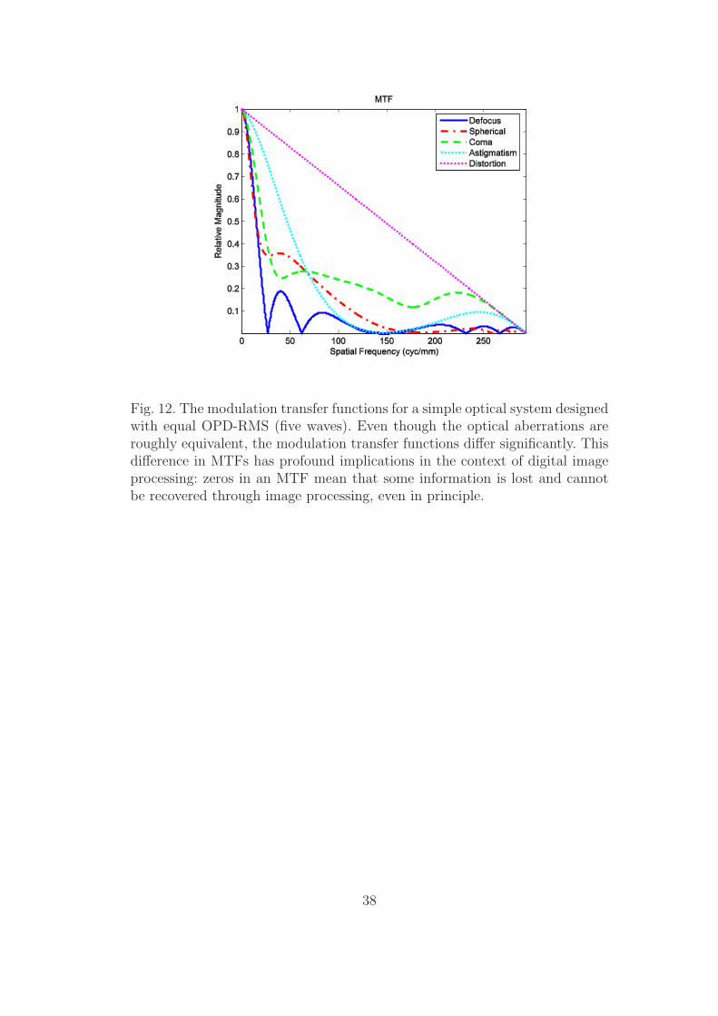
Fig. 12. The modulation transfer functions for a simple optical system designedwith equal OPD-RMS (five waves). Even though the optical aberrations areroughly equivalent, the modulation transfer functions differ significantly. Thisdifference in MTFs has profound implications in the context of digital imageprocessing: zeros in an MTF mean that some information is lost and cannotbe recovered through image processing, even in principle.
38

Detector 4000 x 3Bit-depth 8 bits / color channel
Pixel Pitch (µm) 15fill-factor (%) 75
Quantum Well (electrons) 20kRead Noise (electrons) 50
focal length (mm) 72Wavelengths (µm) 0.486, 0.588, 0.656Object Distance 500 mm
Max. Object Height 150 mm
Table 1. The table contains the general imaging specifications for a 300 dpidocument scanner.
39

Glass Types BK7, F2, BK7Max. Track Length 100 mm
F# 6.0Min. Glass Center Thick. 2 mmMin. Glass Edge Thick. 3 mmMin. Air Center Thick. 4 mmMin. Air Edge Thick. 3 mm
Table 2. The table contains the optical specifications for the triplet lens system.
40