the occam process - karadev.netkaradev.net/uroci/filespdf/files/ee402s-04162009-fjelstad.pdf · the...
TRANSCRIPT

The Occam ProcessThe Occam ProcessAn EnergyAn Energy--efficient Approach to efficient Approach to
Electronic Assembly, Interconnection, Electronic Assembly, Interconnection, and Data Transmission Managementand Data Transmission Management
Joseph FjelstadJoseph FjelstadPresident
Verdant Electronics, Inc.Verdant Electronics, Inc.

IntroductionIntroductionElectronic products are the engine that has propelled the Electronic products are the engine that has propelled the exponential growth of global knowledge over the last half exponential growth of global knowledge over the last half century century
A steady stream of new products from the computer to A steady stream of new products from the computer to the cell phone allow us to connect seamlessly with nearly the cell phone allow us to connect seamlessly with nearly every place and potentially every one on the planet by a every place and potentially every one on the planet by a combination of land lines, wireless transmitters and combination of land lines, wireless transmitters and satellites. satellites.
This comes at a cost however both in terms or materials This comes at a cost however both in terms or materials and energy, both of which have certain limits and there and energy, both of which have certain limits and there are other challenges that we presently face that create a are other challenges that we presently face that create a greater sense of urgency. greater sense of urgency.
We cannot afford to turn off the engine but neither can we We cannot afford to turn off the engine but neither can we continue on the path we are presently on. continue on the path we are presently on.

Comparison of Projected Electricity Use, All Scenarios, 2007 to 2011
Source: US EPA Report to Congress on Server and Data Center Energy Efficiency

Redefining Connection Paths can Help Redefining Connection Paths can Help Reduce Power RequirementsReduce Power Requirements
Capacitance
Impedance changes
Inductance
Signal reflections Dielectric &
conductor loss
Impedance changes Capacitance
Inductance
Signal reflections
Patented

20Gbps High Speed Copper Channel20Gbps High Speed Copper ChannelTechnological Advantages...Technological Advantages...
High speed flex based channel technology High speed flex based channel technology Low power, nonLow power, non--enhanced, link between packages over extended enhanced, link between packages over extended distance, with near zero skew at speeds to >20Gbps per channel. distance, with near zero skew at speeds to >20Gbps per channel. Increased design flexibility and customization for performance Increased design flexibility and customization for performance Chip interconnections and package can be a commodity itemChip interconnections and package can be a commodity itemInterconnection architecture can be standardizedInterconnection architecture can be standardizedAll standard materials All standard materials Compatible with existing packaging assembly technologyCompatible with existing packaging assembly technology
Transmit energy conservation of up to 90%Transmit energy conservation of up to 90%
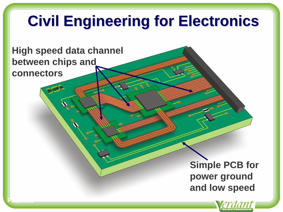
Civil Engineering for ElectronicsCivil Engineering for Electronics
High speed data channel between chips and connectors
Simple PCB for power ground and low speed
Patented

ManufacturingManufacturing’’s Challenges ChallengeAs we progress, energy conservation along with materials As we progress, energy conservation along with materials conservation will become ever more critical to meeting conservation will become ever more critical to meeting the business and social objectives of expanding the reach the business and social objectives of expanding the reach of technology into developing parts of the world. of technology into developing parts of the world.
The challenge is multifaceted and includes a need to The challenge is multifaceted and includes a need to address the environmental impact of these objectivesaddress the environmental impact of these objectives
The European Union passed and enacted in July of 2006 The European Union passed and enacted in July of 2006 its Restriction of Hazardous Substances (its Restriction of Hazardous Substances (RoHSRoHS) ) legislation which among other substances banned lead legislation which among other substances banned lead from electronic solders. from electronic solders.
The impact has been far reaching and has been fraught The impact has been far reaching and has been fraught with technical and economic challengeswith technical and economic challenges
In this environment, an alternative approach to the In this environment, an alternative approach to the manufacture and interconnection electronic assemblies is manufacture and interconnection electronic assemblies is now being developed now being developed

Electronics manufacturing presently comprises three basic Electronics manufacturing presently comprises three basic manufacturing industries: manufacturing industries:
Electronic component manufacturing industry Electronic component manufacturing industry ICs, electronic modules, discrete devices, etc. ICs, electronic modules, discrete devices, etc.
Electronic interconnection manufacturing industryElectronic interconnection manufacturing industryPCBs, package substrates, sockets, connectors, cables, etc.) PCBs, package substrates, sockets, connectors, cables, etc.)
Electronic assembly industryElectronic assembly industrySoldering, testing, box build, etc.Soldering, testing, box build, etc.
Historically vertically integrated companies did it all... Historically vertically integrated companies did it all...
Current Manufacturing ParadigmCurrent Manufacturing Paradigm

Electronics have historically increased functionality of Electronics have historically increased functionality of products while size, weight and cost have all decreased products while size, weight and cost have all decreased with each new generation of productwith each new generation of product
The trend continues but it slope of the curve is flattening The trend continues but it slope of the curve is flattening and becoming more asymptotic. and becoming more asymptotic.
Lead pitches are decreasing, this is impacting both Lead pitches are decreasing, this is impacting both design and manufacture of PCBs and assembliesdesign and manufacture of PCBs and assemblies
Product life and reliability are an ongoing concernProduct life and reliability are an ongoing concern
Lead-free shifts to more expensive metal alloys
Tin whiskers are a wild card issue now in the public eyeTin whiskers are a wild card issue now in the public eye
The Assembly IndustryThe Assembly Industry’’s Challenges Challenge

LeadLead--free concerns in the News free concerns in the News ““RoHSRoHS remains a $30B problemremains a $30B problem””
Design News July 31st 2007Design News July 31st 2007
““EU ban increases worries over 'whiskers' EU ban increases worries over 'whiskers' ““San Jose Mercury News October 8th 2007San Jose Mercury News October 8th 2007
““Peril: Tin Peril: Tin ‘‘whiskerswhiskers’’ that ruin electronicsthat ruin electronics””Corvallis Gazette October 8th 2007Corvallis Gazette October 8th 2007
““Lead PhaseLead Phase--out May Destroy Electronicsout May Destroy Electronics””LA Times October 9th 2007LA Times October 9th 2007
““'Tin whiskers' in electronics stoke anti'Tin whiskers' in electronics stoke anti--lead debatelead debate””San Jose Mercury News October 15th 2007San Jose Mercury News October 15th 2007

The Value of InterconnectionsThe Value of Interconnections
Interconnections have long been undervalued Interconnections have long been undervalued are now gatekeepers of cost and performance are now gatekeepers of cost and performance Interconnections are also commonly the limiting Interconnections are also commonly the limiting factor in product reliability factor in product reliability Improved approaches to design and manufacture Improved approaches to design and manufacture of of electroinicelectroinic interconnections are required to interconnections are required to meet future requirementsmeet future requirements

Solder Solder -- Past and Present IssuesPast and Present Issues
Solder has long been an important technology for Solder has long been an important technology for making electromechanical interconnections and has making electromechanical interconnections and has been reasonably trustworthy.been reasonably trustworthy.
There are some intrinsic problems with solder but tinThere are some intrinsic problems with solder but tin--lead solders have met most challenges lead solders have met most challenges
However component lead contact pitch continues to However component lead contact pitch continues to drop and the problems with solder are becoming drop and the problems with solder are becoming increasing apparent. increasing apparent.
The list things to manage and control in the soldering The list things to manage and control in the soldering process is long and involved. process is long and involved.

Soldering Fishbone DiagramSoldering Fishbone Diagram
Source: Interphase Corporation

The Ongoing Challenge The Ongoing Challenge
Solder

Where are we today?

Current Electronic Manufacturing Process
SCHEMATIC BOM
INVENTORY, STORAGE
PWBDESIGN
ASSEMBLYDESIGN
PARTS ENGINEERING
RELIABILITY ASSURANCE
PROCUREPARTS Storage &
Inventory
PWB FABRICATION
Laminate
Drill
PlateImage
EtchMask
Route
Engineering
SOLDER, PASTE, FLUX
SMT ASSEMBLY
Stencil paste
Inspect
Place parts
Inspect
Reflow
Clean
Inspect
Test

Basic PWB Manufacturing
for Double Sided Boards

Select Appropriate Foil Clad Laminate

Drill Hole Pattern for Vias & Components

Make Through Holes Conductive

Coat Panel with Photoresist

Align Patterned Phototool to Hole Pattern

Expose to UV Light Source

Develop Unexposed Pattern

Plate Copper on to Exposed Pattern Area

Plate Finishing Metal(s) (Solder, Tin, Nickel, Palladium, Gold, etc. either Temporary or Permanent)

Strip Resist from Plated Circuit

Etch Background Copper Foil
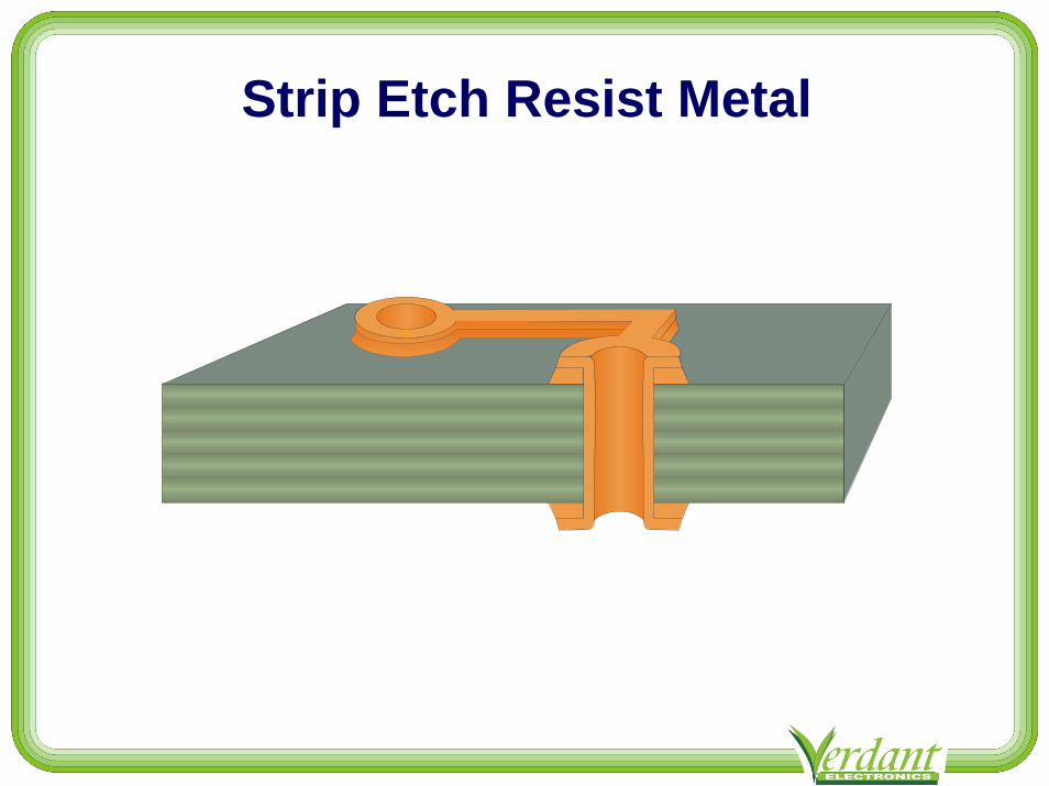
Strip Etch Resist Metal

Coat with Solder Mask (Screen Printed or Photoimaged)

Coat Exposed Copper (solder, electroless Ni/Au or OSP)

Example of Build-up Board Manufacturing Process Steps

Prepare Innerlayers

Laminate Layers

Drill Through Holes

Seed Hole with Conductive Film

Coat with Photoresist

Image Resist Pattern

Plate Copper Traces

Plate Etch Resist Metal

Strip Resist Exposing Base Copper

Etch Background Copper

Strip Etch Resist Metal

Fill Holes with Resin

Coat with Photoimagable or Filled Polymer

Image and Develop or Laser Drill Holes in Polymer

Metallize Surfaces with Copper

Expose and Develop Photoresist

Pattern Plate Copper Circuit Image

Strip Resist & Expose Seed Layer

Etch Copper Seed Layer

Coat with Soldermask

Expose and Develop Soldermask

Apply Solderable Finish (e.g. PbSn)

Basic Process Steps for SMTFixtureStencil solder paste and inspectPlace components and inspectReflow solderClean Underfill critical components DepanelizeTest and rework Ship

1.1. Position and bond various tested components on Position and bond various tested components on a temporary substrate or permanent carriera temporary substrate or permanent carrier
2.2. Encapsulate the tested components in placeEncapsulate the tested components in place
3.3. Remove from substrate, expose terminations.Remove from substrate, expose terminations.
4.4. Interconnect terminations by additive or semiInterconnect terminations by additive or semi--additive board additive board fabfab methods or alternative direct methods or alternative direct interconnection methods.interconnection methods.
Abbreviated Occam ConceptAbbreviated Occam Concept

Sample Sample ProcessProcess
SequenceSequence
Patents pending

The Basic Occam Process
SCHEMATIC BOM
ASSEMBLYDESIGN
PARTS ENGINEERING
PROCUREPARTS
Storage &Inventory
CIRCUITDESIGN Place fully
tested parts
Encapsulate parts
Build up circuits
Test
Singulate
RELIABILITY ASSURANCE

Supply Chain CompressionSupply Chain Compression
Components IC PackagesResistorsCapacitorsInductorsDiodes
Interconnections PCBsSocketsConnectorsCables
Assembly Stencil printingPick and placeReflowCleanBox build
Components IC PackagesResistorsCapacitorsInductorsDiodes
A ssemblyPick and placeCom ponents & ConnectorsEncapsulateBuild up CircuitsBox build
Occam

The Occam Approach is NovelThe Occam Approach is Novel……but Not the Technologiesbut Not the Technologies
• Components can be placed conventionally• Many suitable encapsulants available
• Suitable CTE, low shrinkage, high thermal conductivity• Need not withstand soldering temperatures
• New low pressure molding techniques are available • Many possible options for via creation • Semi-additive fabrication process well established
– Improved process materials coming on line• All copper system both possible and advantageous • Appropriate for all classes of products• Testing and rework... Philosophical questions?
• Why do parts fail? What are the causes of rejects?

Early Early ““KitchenKitchen”” PrototypesPrototypes

Occam Benefits AnalysisOccam Benefits Analysis
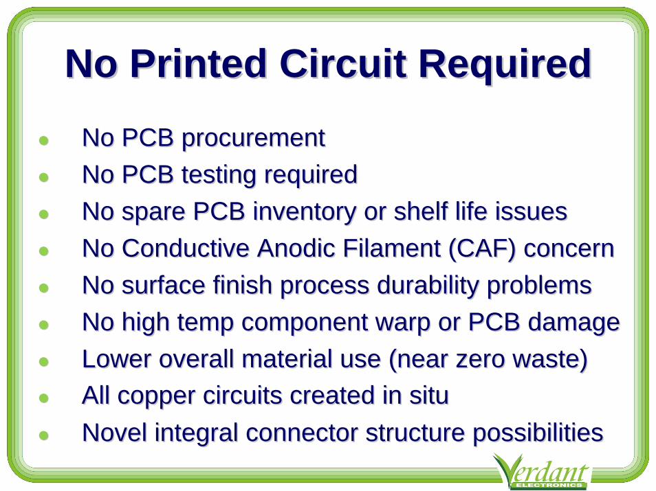
No PCB procurementNo PCB procurementNo PCB testing requiredNo PCB testing requiredNo spare PCB inventory or shelf life issuesNo spare PCB inventory or shelf life issuesNo Conductive Anodic Filament (CAF) concernNo Conductive Anodic Filament (CAF) concernNo surface finish process durability problemsNo surface finish process durability problemsNo high temp component warp or PCB damageNo high temp component warp or PCB damageLower overall material use (near zero waste)Lower overall material use (near zero waste)All copper circuits created in situAll copper circuits created in situNovel integral connector structure possibilities Novel integral connector structure possibilities
No Printed Circuit RequiredNo Printed Circuit Required

Eliminates several manufacturing processesEliminates several manufacturing processesRoHSRoHS restricted material concerns obviatedrestricted material concerns obviatedNo solderability testing or surface finish concerns No solderability testing or surface finish concerns No high temperature damage to devices or PCB No high temperature damage to devices or PCB Energy use is reduced (no bakes or reflow) Energy use is reduced (no bakes or reflow) No solder shorts, opens, micro voids, copper No solder shorts, opens, micro voids, copper dissolution and the host of other common solder dissolution and the host of other common solder related reliability issues and concernsrelated reliability issues and concernsLimited post assembly cleaning & testing issues Limited post assembly cleaning & testing issues
No Soldering RequiredNo Soldering Required

Only fully tested and protected components usedOnly fully tested and protected components usedNo solder build up on tester/socket contacts No solder build up on tester/socket contacts No component leads = No coplanarity issuesNo component leads = No coplanarity issuesNo surface finish solderability issuesNo surface finish solderability issuesFewer component types needed (LGA & QFN)Fewer component types needed (LGA & QFN)Smaller component libraries possible (Smaller component libraries possible (PkgsPkgs) ) Lower cost (simpler) & higher yield on devicesLower cost (simpler) & higher yield on devicesNo MSL issues or popcorning concerns No MSL issues or popcorning concerns Improved routing for area array IC packagesImproved routing for area array IC packagesOverlapping of components is possible Overlapping of components is possible
Reduced Component ConcernsReduced Component Concerns

Overlapping ComponentsOverlapping Components
Patents pending

Package Under Package (Package Under Package (PuPPuP))

Copper Terminated MLCCopper Terminated MLCThin and Thick Film TerminationsThin and Thick Film Terminations
1206 32T Thin Film0805 Thin Film
0805 Thick Film
Thick Film Termination
Thin Film Termination
Clearance (space between the part and the board)
2-4 mils (75 microns typ) >1 mil (20 microns typ)

Components can be placed closer togetherComponents can be placed closer togetherIncreased routing capability Increased routing capability
Occam BenefitsOccam BenefitsCircuit Design SimplificationCircuit Design Simplification

QFP/QFN Routing AdvantageQFP/QFN Routing Advantage
Routing channel opportunities limited on substrate because of solder lands increasing layer count
Routing channel opportunities increased on substrate as circuits can be routed over lands allowing for layer reduction

BGA Routing AdvantageBGA Routing Advantage
Routing channel opportunities limited on both substrate and package
Routing channel opportunities increased on both substrate and packing allowing for layer reduction

The 80% Design Rule ChallengeThe 80% Design Rule Challenge

Effect of Multiple Pitch and Ball VariationEffect of Multiple Pitch and Ball Variation

Effect of Multiple Pitch and Ball VariationEffect of Multiple Pitch and Ball Variation
80% Rule for Pitch with 60% Rule for Pad

A Simpler Alternative?A Simpler Alternative?

Simplifying LayoutSimplifying Layout
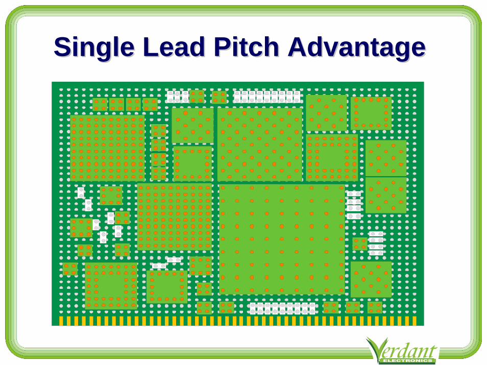
Single Lead Pitch AdvantageSingle Lead Pitch Advantage

Improved Routing = Layer ReductionImproved Routing = Layer Reduction
Courtesy: Happy Holden

HDI HDI -- Price/Density ComparisonPrice/Density Comparison
RCI: Rel price to 8LDEN: Ave pins/sq.inch
Source: Happy Holden

The Future of Electronics?The Future of Electronics?

Components can be placed closer togetherComponents can be placed closer togetherIncreased routing capability Increased routing capability ““DeadDead”” leads ignored for additional routingleads ignored for additional routingSimpler and faster reconfiguration and Simpler and faster reconfiguration and ECOsECOsImproved design security potentialImproved design security potentialIntegral heat spreader redefines placement rulesIntegral heat spreader redefines placement rulesCompleted assemblies can interconnectedCompleted assemblies can interconnected
Occam BenefitsOccam BenefitsCircuit Design SimplificationCircuit Design Simplification
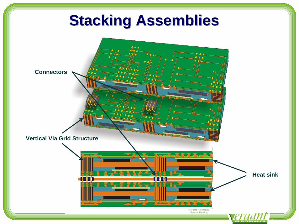
Stacking AssembliesStacking Assemblies
Patents pending
Connectors
Heat sink
Vertical Via Grid Structure

Components can be placed closer togetherComponents can be placed closer togetherIncreased routing capability Increased routing capability Components can be placed closer togetherComponents can be placed closer togetherIncreased routing capability in less space Increased routing capability in less space ““DeadDead”” leads ignored for additional routing spaceleads ignored for additional routing spaceImproved design securityImproved design securityIntegral heat spreader redefine placement rulesIntegral heat spreader redefine placement rulesSimpler and faster reconfiguration and Simpler and faster reconfiguration and ECOsECOsCompleted assemblies can interconnectedCompleted assemblies can interconnectedAdaptable to optoelectronicsAdaptable to optoelectronicsCan be used for flexible circuitsCan be used for flexible circuits
Occam BenefitsOccam BenefitsCircuit Design SimplificationCircuit Design Simplification

Simple structures with fewer elementsSimple structures with fewer elementsLower temperature processing avoids thermal Lower temperature processing avoids thermal damage caused by leaddamage caused by lead--free soldering free soldering Components are fully encapsulated increasing Components are fully encapsulated increasing shock and vibration immunityshock and vibration immunityHermetic structure possibilities with full metal Hermetic structure possibilities with full metal jacket protection jacket protection Total EMI and ESD protection possibilitiesTotal EMI and ESD protection possibilitiesIntegral heat spreader improves device lifeIntegral heat spreader improves device life
Occam BenefitsOccam BenefitsReliability ImprovementReliability Improvement

Solderless Assembly Allows Thermal Solderless Assembly Allows Thermal Concerns to Be Addressed UpfrontConcerns to Be Addressed Upfront
Patents pending

Testing is believed to be criticalTesting is believed to be critical…… Why?Why?Most testing is predicated on the anticipation of Most testing is predicated on the anticipation of manufacturing related defects and manufacturing related defects and faultsfaults
Shorts and opens are accepted as facts of lifeShorts and opens are accepted as facts of lifeLeadLead--free assembly damage to assembly components free assembly damage to assembly components
Current assembly technology has limitsCurrent assembly technology has limitsSimpler processes should yield higher Simpler processes should yield higher The ultimate test is assembly turn onThe ultimate test is assembly turn onCan time and money for test be better allocated?Can time and money for test be better allocated?
What about Testing?What about Testing?

Stig Oresjo “Blending Test Strategies for Limited-Access Boards” Circuits Assembly Aug 2002
What and Where are the Problems? What and Where are the Problems?

Simple Cost Simple Cost Comparison Comparison
ModelModel

Conventional SMT LineConventional SMT Line
Water Wash Machine$80K
Solder Paste Measurement Station $15K
Kitting, Feeder Setup
Solder Printer$75K
P&P Machine$200K
Reflow Oven$55K
Ionograph
$15K
X-ray$50K
Equipment with ~capital cost
Source: Richard Otte, Promex Industries
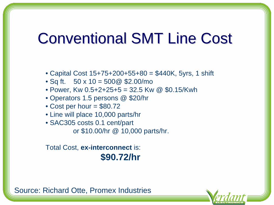
• Capital Cost 15+75+200+55+80 = $440K, 5yrs, 1 shift• Sq ft. 50 x 10 = 500@ $2.00/mo• Power, Kw 0.5+2+25+5 = 32.5 Kw @ $0.15/Kwh• Operators 1.5 persons @ $20/hr• Cost per hour = $80.72• Line will place 10,000 parts/hr• SAC305 costs 0.1 cent/part
or $10.00/hr @ 10,000 parts/hr.
Total Cost, ex-interconnect is:$90.72/hr
Conventional SMT Line CostConventional SMT Line Cost
Source: Richard Otte, Promex Industries

Occam Process LineOccam Process Line
Water Wash Machine
Solder Paste Measurement Station
Kitting, Feeder Setup
Solder Printer P&P Machine$200K
Reflow Oven
Encapsulant Dispenser $75K
Encapsulant Cure Station $5K
X-ray
Ionograph
Interconnectdeposition $?
Source: Richard Otte, Promex Industries

Occam Process Line CostOccam Process Line Cost
• Capital Cost 200+75+5 = $280K• Sq ft. 20 x 10 = 200• Power, Kw 2+1+5 = 8 Kw• Operators 1.0 person• Cost per hour = $50.38• Line will place 10,000parts/hr• Encapsulant costs 2 cents/cc
or 0.4cents/cm2 @ 2 mm thicknessor 0.1cents/pt. @4 parts/ccor $10.00/hr @ 10,000 pts/hr.
Total cost, ex-interconnect is:$60.38/hr, 33% less
Source: Richard Otte, Promex Industries

AlternativeAlternativeSolderless StructuresSolderless Structures

Alternative Solderless StructuresAlternative Solderless Structures
programmed
Patents Pending

Direct WriteDirect Write
Patents Pending
Rapid prototyping potential is compelling

CoCo--Design to Compress TimeDesign to Compress Time
IC Design Package Design PCB DesignIC Design Package Design PCB Design
Time to Market Reduction

Occam Roadmap Occam Roadmap Proof of concept Proof of concept Test vehicle identification and reliability testingTest vehicle identification and reliability testingStandards development Standards development –– for design and performancefor design and performanceSimple products first (like early SMT) Simple products first (like early SMT) Increase complexity with captured experienceIncrease complexity with captured experienceExplore alternative solderless assembly methodsExplore alternative solderless assembly methodsEngage Material & Equipment Suppliers with new product Engage Material & Equipment Suppliers with new product and process opportunities and process opportunities Suitable materials identified and characterizedSuitable materials identified and characterizedProcess qualification and technology transfer Process qualification and technology transfer

Alternative Future?Alternative Future?

Thank youThank you
“A mind, once stretched by a new idea, never returns to its
original dimensions.”
~ Oliver Wendell Holmes ~American Philosopher and Jurist