the microwave response of ultra thin microcavity arrays
TRANSCRIPT

1
THE MICROWAVE RESPONSE OF
ULTRA THIN MICROCAVITY ARRAYS
Submitted by
JAMES ROBERT BROWN
To the University of Exeter
as a thesis for the degree of
Doctor of Philosophy
June 2010
This thesis is available for library use on the understanding that it is copyright material
and that no quotation from this thesis may be published without proper
acknowledgement.
I certify that all material in this thesis which is not my own work has been identified and
that no material has previously been submitted and approved for the award of a degree
by this or any other University.
______________________________

2
Abstract
The ability to understand and control the propagation of electromagnetic radiation underpins a
vast array of modern technologies, including: communication, navigation and information
technology. Therefore, there has been much work to understand the interaction between
electromagnetic waves and metal surfaces, and in particular to design materials the
characteristics of which can be tailored to produce a desired response to microwave radiation. It
is the objective of this thesis to demonstrate that patterning metal surfaces with sub-wavelength
apertures can afford hitherto unrealised control over the reflection and transmission
characteristics of materials which are an order of magnitude thinner than those employed
historically.
The work presented herein aims to establish ultra thin cavity structures as novel materials for
the selective absorption and transmission of microwave radiation. Experimental and theoretical
approaches are used to elucidate the mechanism that allows such structures to produce highly
efficient absorption via the excitation of standing wave modes in structures that are two orders
of magnitude thinner than the operating wavelength. Also considered is how this same
mechanism mediates transmission of selected frequencies through similarly thin structures.
Later chapters focus on ultra thin cavity structures which, through higher-order rotational
symmetry, exhibit resonant absorption which is almost completely independent of incident and
azimuthal angle and polarisation state. A detailed studied of the absorption bandwidth of these
devices is also presented in the context of fundamental theoretical limitations arising from the
thickness and magnetic permeability of the structure.

3
This thesis is dedicated to my wonderful Sharmi: now that it is finished we
get our weekends back!

4
It is best to keep an open mind, but not so open that one’s brain falls out.
Richard Dawkins, 2007

5
Table of contents
ABSTRACT______________________________________________________________ 2
TABLE OF CONTENTS____________________________________________________5
LIST OF FIGURES AND TABLES___________________________________________9
LIST OF ABBREVIATIONS________________________________________________19
ACKNOWLEDGEMENTS_________________________________________________20
CHAPTER 1:
Introduction ______________________________________________________________23
CHAPTER 2:
The interaction of microwaves with metal surfaces
2.1 Introduction___________________________________________________________25
2.2 The scattering of electromagnetic radiation by matter__________________________25
2.2.1 Radar Cross Section (RCS)____________________________________________26
2.2.2 Electromagnetic scattering regimes _____________________________________30
2.2.2.1 Rayleigh scattering_______________________________________________30
2.2.2.2 Resonant scattering_______________________________________________30
2.2.2.3 Optical scattering________________________________________________31
2.2.3 Scattering from periodically textured surfaces_____________________________33
2.2.3.1 The phenomenon of diffraction _____________________________________33
2.2.3.2 Diffraction gratings_______________________________________________34
2.3 Surface waves_________________________________________________________36
2.3.1 Surface wave excitation ______________________________________________37
2.4 Materials for the absorption of microwave radiation ___________________________40
2.4.1 Underpinning absorption mechanisms ___________________________________40
2.4.2 Conventional absorbing materials_______________________________________44
2.5 Current research in electromagnetic materials ________________________________47
2.6 Important applications for absorbing materials _______________________________49

6
CHAPTER 3:
Modelling
3.1 Introduction___________________________________________________________53
3.2 The finite element approach______________________________________________ 53
3.3 An overview of HFSS___________________________________________________ 54
3.3.1 Assembling the structure to be simulated_________________________________ 54
3.3.2 Assigning material properties__________________________________________ 55
3.3.3 Boundary conditions_________________________________________________ 57
3.3.4 Excitations_________________________________________________________60
3.3.5 Meshing___________________________________________________________61
3.3.6 Post-processing _____________________________________________________64
3.4 Modelling approaches used in this thesis ____________________________________65
3.4.1 Mono-grating reflection structures _____________________________________ 65
3.4.2 Mono-grating transmission structures ___________________________________ 68
3.4.3 Bi-grating reflection structures ________________________________________ 70
3.4.4 Tri-grating reflection structures ________________________________________ 72
3.4.5 Broadband structures ________________________________________________ 77
3.4.5.1 Non-parallel slits_________________________________________________77
3.4.5.2 Multi-layer structures _____________________________________________79
3.5 Summary_____________________________________________________________80
CHAPTER 4:
The microwave reflectivity and transmissivity of a low-loss dielectric layer disposed between
two metallic layers perforated periodically by sub-wavelength slits
4.1 Introduction___________________________________________________________81
4.2 Background___________________________________________________________82
4.3 Experimental__________________________________________________________84
4.3.1 Fabrication of samples_______________________________________________ 84
4.3.2 Definition of polarisation state, angles of incidence and azimuth______________ 87

7
4.3.3 Measurement of microwave reflectivity and transmissivity___________________87
4.3.3.1 Focused horn____________________________________________________87
4.3.3.2 Long path length azimuthal scan apparatus____________________________ 88
4.4 Results and discussion__________________________________________________ 90
4.4.1 Reflection sample___________________________________________________ 90
4.4.2 Optimisation of resonance depth_______________________________________ 97
4.4.2.1 Optimisation by altering core material properties_______________________101
4.4.2.2 Optimisation by altering core thickness_______________________________103
4.4.2.3 Optimisation by altering slit width__________________________________ 106
4.4.3 Polarisation conversion effects________________________________________ 108
4.4.4 Transmission samples_______________________________________________ 110
4.4.4.1 Aligned slits ___________________________________________________ 110
4.4.4.2 Off-set slits ____________________________________________________114
4.5 Summary____________________________________________________________ 116
CHAPTER 5:
Reduction of azimuthal and incident angle sensitivity and polarisation conversion effects – bi-
gratings
5.1 Introduction__________________________________________________________118
5.2 Experimental_________________________________________________________118
5.3 Results______________________________________________________________119
5.4 Polarisation conversion effects___________________________________________126
5.5 Dispersion___________________________________________________________129
5.6 Conclusions__________________________________________________________130
CHAPTER 6:
Minimisation of azimuthal and incident angle sensitivity and polarisation conversion effects –
tri-gratings
6.1 Introduction__________________________________________________________132

8
6.2 Experimental details___________________________________________________133
6.3 Theory______________________________________________________________134
6.4 Results______________________________________________________________136
6.4.1 Tri-grating sample 1________________________________________________ 136
6.4.2 Tri-grating sample 1 – polarisation conversion___________________________ 144
6.4.3 Tri-grating sample 2________________________________________________146
6.4.4 Tri-grating sample 2 – polarisation conversion___________________________ 153
6.5 Summary_____________________________________________________________ 154
CHAPTER 7:
Methods for achieving maximum absorption bandwidth
7.1 Introduction__________________________________________________________156
7.2 Experimental ________________________________________________________ 157
7.3 Theory______________________________________________________________160
7.4 Results______________________________________________________________163
7.4.1 Standard mono-grating______________________________________________163
7.4.2 Structure 1 – multiple discrete repeat periods ____________________________165
7.4.3 Structure 2 – multiple continuous repeat periods__________________________168
7.4.4 Structure 3 - Multi-layering __________________________________________172
7.4.5 Structure 4 - Multiple permittivities ___________________________________175
7.5 Conclusions _________________________________________________________178
CHAPTER 8:
Conclusions
8.1 Summary of thesis_____________________________________________________180
8.2 Ideas for future work___________________________________________________182
8.3 List of publications ____________________________________________________186
REFERENCES___________________________________________________________188

9
List of figures and tables
Figure 2.1 RCS for a metallic sphere. The circumference is given in wavelengths and the RCS is
normalised to the actual cross sectional area of the sphere (this figure has been adapted from
Knott (1993))________________________________________________________________32
Figure 2.2 A p-polarised wave incident on a grating structure (a) 3-D projection (b) plan
view_______________________________________________________________________35
Figure 2.3 A p-polarised electromagnetic wave incident on the interface between two media
___________________________________________________________________________37
Figure 2.4 Diagramatical representation of the plasmon dispersion relation_______________39
Figure 2.5 Waves incident on a typical absorbing material____________________________42
Figure 2.6 Plot of the simulated reflectivity of a Dallenbach layer for a p-polarised wave at
different angles of incidence___________________________________________________44
Figure 2.7 A typical Salisbury screen (a) geometry (b) simulated reflectivity for a p-polarised
wave over a range of incident angles_____________________________________________46
Figure 3.1 Plots of typical finite element meshes constructed using HFSS (a) 3-D projection of
the initial mesh for a typical microcavity structure, 1258 tetrahedra (b) cropped 2-D side
elevation of the initial mesh for a typical microcavity structure, 1258 tetrahedra (c) 3-D
projection of the final mesh for typical microcavity structure 43401 tetrahedra (d) cropped 2-D
side elevation of the final mesh for typical microcavity structure 43401 tetrahedra_________62
Figure 3.2 Mono-grating structure as modelled in HFSS (a) Selected Dimensions and materials
(b) Boundary conditions_______________________________________________________66
Figure 3.3 Finite element mesh for the mono-grating reflection structure (a) 3-D projection (b)
Cropped 2-D projection, metal layers marked by black lines___________________________68
Figure 3.4 Diagram of the off-set transmission structure______________________________69

10
Figure 3.5 Diagram showing the bi-grating model (a) the model geometry (b) the finite element
mesh_______________________________________________________________________72
Figure 3.6 The tri-grating sample geometries (not to scale) and the co-ordinate system used
(a) 3-D projection of tri-grating 1 (b) 3-D projection of tri-grating 2, tm = 18 μm, tc = 356 μm, ws
= 0.3 mm, 12 gg = 10 mm, is the polar angle, is the azimuthal angle_____________74
Figure 3.7 Forming the tri-grating structures without inputting irrational numbers (a) metal plate
(30 x 30) mm with three slits spaced 10 mm apart (b) second set of slits added and rotated by
60° about the z-axis (c) third set of slits added and rotated by -60° about the z-axis (d)
translation of first set of slits by 5 mm in the z-direction (e) subtraction of all three sets of slits
from the metal layer, two unit cells can be seen_____________________________________75
Figure 3.8 Plots of selected parts of the final finite element mesh for the tri-grating structures
(a) for tri-grating 1 (b) for tri-grating 2____________________________________________77
Figure 3.9 Multiple continuous repeat periods with alternate saw-tooth slits_______________78
Figure 3.10 Multi-layer microcavity structure (a) 3-D projection of multi-layer structure, 2
periods shown (b) end projection of multi-layer_____________________________________79
Figure 4.1 Cross-section through the substrate material The dielectric core is FR4 – a Glass
Reinforced Plastic (GRP) composite material with a permittivity of (4.17 + i0.07) _________85
Figure 4.2 Cross-section through the microcavity samples (a) the reflection sample (b) the first
transmission sample with slits perfectly aligned (c) the second transmission sample with slits
perfectly mis-aligned _________________________________________________________86
Figure 4.3 Definition of polarisation state, incident () and azimuthal () angle (a) TE or s-
polarised – the E-vector is perpendicular to the plane of incidence (b) TM or p-polarised – the
E-vector is contained within the plane incidence ____________________________________87
Figure 4.4 Photograph of the focused horn apparatus The VNA can be seen in the
background, the reference aperture can be seen in the centre. The focal length of the
system is adjusted by a stepper motor attached to the nearest mirror (out of shot to the
left)_________________________________________________________________88

11
Figure 4.5 Schematic of the long path length, azimuthal-scan apparatus set up for measurements
of bi-static reflectivity_________________________________________________________89
Figure 4.6 Schematic of the long path length, azimuthal-scan apparatus set up for measurements
of transmission_______________________________________________________________90
Figure 4.7 Experimental Reflected intensities for reflection sample shown as greyscale plots (a)
Rpp data as a function of frequency and azimuthal angle at º16 (b) Rss data as a function of
frequency and azimuthal angle at º16 (c) Rpp data as a function of frequency and azimuthal
angle at º57 , dashed line corresponds to expected position of diffraction edge (d) Rss data
as a function of frequency and azimuthal angle at º57 ____________________________91
Figure 4.8 Line plots of the reflectivity of the reflection sample as measured experimentally at
incident angles of 16 and 4.57 for (a) p-polarisation and 0 (b) s-polarisation
and 90 _______________________________________________________________ 93
Figure 4.9 Reflectivity of the reflection sample as measured experimentally and simulated by
the finite element model: P-polarisation incident at 4.57 and 0 _______________ 94
Figure 4.10 Behaviour of the electric field within the dielectric core of the ultra thin cavities as
simulated by the finite element model (a) Instantaneous magnitude of the electric field at 7.1
GHz, plotted at a phase corresponding to peak field strength, the black line represent the copper
layers, blue corresponds to 0 V/m, red corresponds to 20 v/m, incident wave amplitude 1 V/m
(b) z-component of the electric field along a line through the centre of the core parallel to the x-
axis (c) Instantaneous the electric field vector at 7.1 GHz, plotted at a phase corresponding to
peak field strength, blue corresponds to 0 V/m, red corresponds to 20 v/m, incident wave
amplitude 1 V/m_____________________________________________________________ 95
Figure 4.11 Waves incident on the ultra thin cavity structure__________________________97
Figure 4.12 Reflectivity of the ultra-thin cavity structure as a function of frequency for
different values of imaginary permittivity as simulated using the finite element model (a) for
values of imaginary permittivity (eps’’) between 0.02 and 0.2 (b) for values of imaginary
permittivity (eps’’) between 0.2 and 0.9_________________________________________102
Figure 4.13 Field plots showing the instantaneous magnitude of the electric field for different
values of imaginary permittivity, scale runs from 0 V/m (blue) to 50 V/m (red), incident wave

12
amplitude was 1 V/m in all cases (a) imaginary permittivity = 0.02 (b) imaginary permittivity =
0.08 (c)imaginary permittivity = 0.2 (d) imaginary permittivity = 0.4 (e) imaginary permittivity
= 0.9_____________________________________________________________________103
Figure 4.14 Reflectivity versus frequency as predicted by the finite element model for structures
of differing core thickness_____________________________________________________104
Figure 4.15 Field plots showing the instantaneous magnitude of the electric field for different
core thicknesses, scale runs from 0 V/m (blue) to 40 V/m (red) and the incident wave amplitude
was 1V/m in all cases (a) core thickness = 100 μm (b) core thickness = 120 μm (c) core
thickness = 150 μm (d) core thickness = 180 μm (e) core thickness = 250 μm (f) core thickness
= 356 μm __________________________________________________________________106
Figure 4.16 Reflectivity as a function of frequency for the ultra thin cavity arrays with different
slit widths_________________________________________________________________107
Figure 4.17 Experimental polarisation-converted reflected intensities for reflection sample
shown as greyscale plots (a) Rps data as a function of frequency and azimuthal angle at
º16 (b) Rsp data as a function of frequency and azimuthal angle at º16 (c) Rps data as a
function of frequency and azimuthal angle at º57 (d) Rsp data as a function of frequency
and azimuthal angle at º57 ________________________________________________110
Figure 4.18 Transmission as a function of frequency for the aligned slit structure as measured
using the focused horn system and simulated using the finite element model ____________110
Figure 4.19 Plots of the electric field at 7.2 GHz for the aligned transmission structure: blue
corresponds to 0 V/m and red to 20 V/m and the incident wave amplitude was 1 V/m (a) the
instantaneous magnitude of the electric field plotted at a phase corresponding to peak field (b)
the instantaneous electric field vector plotted at a phase corresponding to peak
field______________________________________________________________________111
Figure 4.20 Plots of the instantaneous magnitude of the electric field at different frequencies for
the aligned transmission structure, scale runs from 0 V/m (blue) to 20 V/m (red) and the
incident wave amplitude was 1 V/m in all cases (a) 7.2 GHz (b) 7.4 GHz (c) 7.6
GHz______________________________________________________________________114
Figure 4.21 Transmission as a function of frequency for the off-set slit structure as measured
using the focused horn system and simulated using the finite element model____________114

13
Figure 4.22 Plots of the electric field at 13.12 GHz for the off-set transmission structure, scale
runs from 0 V/m (blue) to 20 V/m (red) and the incident wave amplitude was 1 V/m in both
cases (a) the instantaneous magnitude of the electric field plotted at a phase corresponding to
peak field (b) the instantaneous electric field vector plotted at a phase corresponding to peak
field______________________________________________________________________115
Figure 5.1 (a) The mono-grating sample geometry (not to scale) and the co-ordinate system
used: θ is the polar angle, is the azimuthal angle, λg = 10 mm, ws = 0.3 mm (b) 3-D
projection of the bi-grating, λg1 = λg2 (c) Cross-section through the bi-grating structure, tm = 18
μm, tc = 356 μm, ws = 0.3 mm, λg2 = λg1 =10 mm, sample area 500 mm by 500 mm_______119
Figure 5.2 Reciprocal space diagram for the bi-grating______________________________120
Figure 5.3 Bi-grating sample (a) Experimental Rpp data as a function of frequency and
azimuthal angle at = 57° (b) Experimental Rss data as a function of frequency and azimuthal
angle at = 57° (c) Line plot showing comparison of measured data to the predictions of the
numerical model: Rpp = 57°, = 45° (d) Prediction of the electric field vector distribution at
a phase corresponding to peak field strength on the upper surface of the lower metal layer for a
{1, 1} mode at 10.93 GHz: the longest arrows correspond to enhancements of 13 times the
injected field_______________________________________________________________121
Figure 5.4 Bi-grating sample (a) Incident wavevector and electric vectors on the lower surface
of a metal patch, and the resulting charge distribution for: = 0°, p-polarization (b) = 0°, s-
polarization (c) = 45°, p-polarization and (d) = 45°, s-polarization________________123
Figure 5.5 Distribution of the electric field on the upper surface of the lower metal layer plotted
at a phase corresponding to maximum field (a) The (2,0) mode at = 90° and 13.9 GHz (b)
The (0,2) mode at = 0° and 13.9 GHz (c) The degenerate (2,0) and (0,2) modes at = 45°,
at 14.55 GHz (d) The (2,1) mode at = 45°, 16.6 GHz_____________________________125
Figure 5.6 Experimental polarisation-converted reflected intensities for reflection sample
shown as greyscale plots (a) Rps data as a function of frequency and azimuthal angle at
º16 (b) Rsp data as a function of frequency and azimuthal angle at º16 (c) Rps data as a
function of frequency and azimuthal angle at º57 (d) Rsp data as a function of frequency
and azimuthal angle at º57 ________________________________________________127

14
Figure 5.7 Distribution of the electric field on the upper surface of the lower metal layer plotted
at a phase corresponding to maximum field for the degenerate (2, 0) and (0, 2) modes as
excited by an s-polarised wave = 45°, 4.57 at a frequency of 14.585 GHz________129
Figure 5.8 Dispersion plots determined from the frequency of the modes supported by the bi-
grating sample at = 0° and 45º with (a) p-polarized and (b) s-polarization incident
radiation__________________________________________________________________130
Figure 6.1 The tri-grating sample geometries (not to scale) and the co-ordinate system used:
is the polar angle, is the azimuthal angle, g = 10 mm, ws = 0.3 mm (a) 3-D projection of tri-
grating 1 (b) 3-D projection of tri-grating 2 (c) Cross-section through the tri-grating structure,
one set of slits shown for clarity, tm = 18 μm, tc = 356 μm, ws = 0.3 mm, 12 gg =10 mm,
sample area 500 mm by 500 mm_______________________________________________133
Figure 6.2 Reciprocal space diagrams for the tri-gratings showing: (a) the scattering vectors
and reciprocal lattice points (b) with a series of circles centred on the origin having radii at
which resonant modes are expected_____________________________________________135
Figure 6.3 Tri-grating sample 1: (a) Experimental Rpp data as a function of frequency and
azimuthal angle at 16 ; (b) Experimental Rss data as a function of frequency and azimuthal
angle at 16 ; (c) Experimental Rpp data as a function of frequency and azimuthal angle
at 43 ; (d) Experimental Rss data as a function of frequency and azimuthal angle
at 43 _________________________________________________________________137
Figure 6.4 Tri-grating samples 1 and 2: (a) Line plot showing comparison of measured data to
the predictions of the numerical model for tri-grating 1: Rpp 43 , 30 ; (b) Line plot
showing comparison of measured data to the predictions of the numerical model for tri-grating
2: Rpp 43 , 30 ______________________________________________________139
Figure 6.5 Tri-grating sample 1: predictions of the electric field vector distribution at phases
corresponding to peak field strengths on the upper surface of the lower metal layer for: (a) an
8.35 GHz, p-polarised wave incident at 43 90 ; (b) an 8.35 GHz, s-polarised wave
incident at 43 90 ; (c) a 15 GHz, p-polarised wave incident at 43 90 ; (d)
a 15 GHz, s-polarised wave incident at 43 90 , the longest arrows correspond to
enhancements of 15 times in all cases___________________________________________141

15
Figure 6.6 Diagrams showing the incident electric field and resulting charge distribution for a
15 GHz s-polarised wave incident at (e) 90 ; (f) 60 ______________________143
Figure 6.7 Tri-grating sample 1: predictions of the electric field vector distribution at phases
corresponding to peak field strengths on the upper surface of the lower metal layer for: (a) an
17.3 GHz, p-polarised wave incident at 43 , 90 ; (b) a 17.8 GHz, p-polarised wave
incident at 43 , 90 , the longest arrows correspond to enhancements of 15 times in
both cases_________________________________________________________________144
Figure 6.8 Experimental polarisation-converted reflected intensities for tri-grating sample 1
shown as greyscale plots (a) Rps data as a function of frequency and azimuthal angle at
º16 (b) Rsp data as a function of frequency and azimuthal angle at º16 (c) Rps data as a
function of frequency and azimuthal angle at º43 (d) Rsp data as a function of frequency
and azimuthal angle at º43 ________________________________________________145
Figure 6.9 Tri-grating samples 1 and 2: (a) Experimental Rpp data as a function of frequency
and azimuthal angle at 16 for tri-grating sample 2; (b) Experimental Rss data as a function
of frequency and azimuthal angle at 16 for tri-grating sample 2; (c) Experimental Rpp data
as a function of frequency and azimuthal angle at 43 for tri-grating sample 2; (d)
Experimental Rss data as a function of frequency and azimuthal angle at 43 for tri-grating
sample 2 (e) Experimental Rpp data as a function of frequency and azimuthal angle
at 43 for tri-grating sample 1; (f) Experimental Rss data as a function of frequency and
azimuthal angle at 43 for tri-grating sample 1________________________________147
Figure 6.10 Tri-grating sample 2: predictions of the electric field vector distribution at phases
corresponding to peak field strengths on the upper surface of the lower metal layer for: (a) an
8.1 GHz, p-polarised wave incident at 43 , 60 ; (b) a 8.1 GHz, s-polarised wave
incident at 43 , 60 ; (c) a 13.8 GHz, p-polarised wave incident at 43 , 60 ;
(d) a 13.8 GHz, s-polarised wave incident at 43 , 60 , the longest arrows correspond
to enhancements of 15 times in all cases_________________________________________151
Figure 6.11 Tri-grating sample 2: (a) prediction of the electric field vector distribution at a
phase corresponding to peak field strength on the upper surface of the lower metal layer for: a
16.4 GHz, p-polarised wave incident at 43 , 60 ; (b) diagram showing the incident
electric field and resulting charge distribution for a p-polarised wave incident at 90 ; (c)
diagram showing the incident electric field and resulting charge distribution for a s-polarised
wave incident at 90 ____________________________________________________152

16
Figure 6.12 Tri-grating sample 2: (a) prediction of the electric field vector distribution at a
phase corresponding to peak field strength on the upper surface of the lower metal layer for: a
17.1 GHz, s-polarised wave incident at 43 , 60 ; (b) prediction of the electric field
vector distribution at a phase corresponding to peak field strength on the upper surface of the
lower metal layer for: a 18.3 GHz, s-polarised wave incident at 43 , 60 _______153
Figure 6.13 Experimental polarisation-converted reflected intensities for tri-grating sample 2
shown as greyscale plots (a) Rps data as a function of frequency and azimuthal angle at
º16 (b) Rsp data as a function of frequency and azimuthal angle at º16 (c) Rps data as a
function of frequency and azimuthal angle at º43 (d) Rsp data as a function of frequency
and azimuthal angle at º43 ________________________________________________154
Figure 7.1 The microcavity structure geometries (not to scale) and the co-ordinate system used:
θ is the incident angle, is the azimuthal angle, ws is the slit width, g is the repeat period of
the structure (a) 3-D projection of a standard mono-grating structure in which all slits run
parallel (b) Cross-section through the standard mono-grating structure (c) 3-D projection of
Structure 1, multiple discrete repeat periods (d) Plan view projection of Structure 2, multiple
continuous repeat periods with alternate saw-tooth slits (e) 3-D projection of Structure 3, multi-
layer structure, 2 periods shown (f) end projection of Structure 3, multi-layer structure, 2
periods shown (g) 3-D projection of Structure 4, multiple refractive
indices___________________________________________________________________159
Figure 7.2 Response of an example Salisbury screen absorber as predicted using the finite
element model (a) reflectivity in decibels versus frequency (b) reflectivity in decibels versus
wavelength________________________________________________________________160
Figure 7.3 Theoretical and experimental data for standard mono-grating (a) Reflectivity in
decibels versus wavelength as predicted by the finite element model and measured
experimentally (b) Reflectivity in decibels versus wavelength as predicted by the finite element
model for mono-grating structures of differing core thickness (c) Percent of narrowband
bandwidth limit versus core thickness for the a series of mono-grating
structures_________________________________________________________________164
Figure 7.4 Multiple discrete period structures (a) Reflectivity in decibels versus wavelength for
structure with dielectric core thickness of 190 μm (b) Reflectivity in decibels versus
wavelength as predicted by the finite element model for multiple discrete period structures of

17
differing core thickness (c) Percent of narrowband bandwidth limit versus core thickness for
the a series of multiple discrete period structures (d) Cross-section of modified multiple
discrete repeat period structure, (e) Reflectivity in decibels versus wavelength as predicted by
the finite element model for multiple discrete period structures with different values of t2
_________________________________________________________________________167
Figure 7.5 Multiple continuous period structures (a) Reflectivity in decibels versus wavelength
as predicted by the finite element model and measured experimentally (b) Reflectivity in
decibels versus wavelength as predicted by the finite element model for multiple continuous
period structures of differing core thickness (c) Percent of narrowband bandwidth limit versus
core thickness for the a series of multiple continuous period structures (d) Plot of the
instantaneous electric field vector on the upper surface of the lower metal layer at a wavelength
of 47 mm and a phase corresponding to peak field, the longest arrows correspond to 30 V/m
(an enhancement of 30 times the incident field), dashed lines added to indicate position of slits
(e) Plot of the magnitude of the instantaneous electric field on the upper surface of the lower
metal layer at a wavelength of 40 mm and a phase corresponding to peak field, dark blue areas
correspond to 0 V/m, green areas to 20 V/m (f) Plot of the magnitude of the instantaneous
electric field on the upper surface of the lower metal layer at a wavelength of 36 mm and a
phase corresponding to peak field, dark blue areas correspond to 0 V/m, green areas to 20 V/m
and red areas to 30 V/m______________________________________________________171
Figure 7.6 Multi-layer structures (a) Reflectivity in decibels versus wavelength for structure
with dielectric core thicknesses t1 = 0.13 mm, t2 = 0.12 mm, t3 = 0.1 mm, t4 = 0.075 mm, (b)
magnitude of the electric field at a wavelength of 20.2 mm and at a phase corresponding to
peak field for the N = 1 mode, scale runs from 0 V/m to 90 V/m (c) magnitude of the electric
field at a wavelength of 20.2 mm and at a phase corresponding to peak field for the N = 3
mode, scale runs from 0 V/m to 15 V/m (d) magnitude of the electric field at a wavelength of
20.9 mm and at a phase corresponding to peak field for the N = 1 mode, scale runs from 0 V/m
to 50 V/m (e) magnitude of the electric field at a wavelength of 20.2 mm and at a phase
corresponding to peak field for the N = 3 mode, scale runs from 0 V/m to 20 V/m________173
Figure 7.7 Multiple-permittivity structure (a) Reflectivity in decibels versus wavelength for
structures with a range of dielectric core thicknesses (b) Percent of narrowband bandwidth
limit versus core thickness for the series of multiple-permittivity structures (d) Reflectivity in
decibels versus wavelength as predicted by the finite element model for multiple-permittivity
structures with different values of loss tangent in the cavity with εr = 3.5 _______________177

18
Figure 8.1 Hybrid transmission structures (a) array of slits in the upper metal layer, single slit
in the lower metal layer (b) rotation of slits in lower metal layer relative to those in the upper
metal layer, layers shown separately (c) progressive reduction in slit number to concentrate
field_____________________________________________________________________183
Figure 8.2 Pseudo-fractal multi-layer absorbing structure___________________________184
Figure 8.3 Absorbing structures in which each cavity contains dielectric media of different
refractive index____________________________________________________________185
Table 7.1 Resonant wavelengths in millimetres for Structure 4 – Multi-layer structure as
predicted using (7.4) and observed using HFSS___________________________________174

19
List of abbreviations
E-Vector – electric field vector
FEA – Finite Element Analysis
GRP – Glass Reinforced Plastic
HFSS – High Frequency Structure Simulator (software)
MathCAD – Mathematical Computer Aided Design (software)
PCB – Printed Circuit Board
Q-Factor – Quality Factor
RCS – Radar Cross Section
RF – Radio Frequency
Rpp – reflection coefficient when both receiver and transmitter are p-polarised
Rps – reflection coefficient when transmitter is p-polarised and receiver is s-polarised
Rsp – reflection coefficient when transmitter is s-polarised and receiver is p-polarised
Rss – reflection coefficient when both receiver and transmitter are s-polarised
TE – Transverse Electric polarisation (s-polarised)
TM – Transverse Magnetic polarisation (p-polarised)
VNA – Vector Network Analyser
m - microns

20
Acknowledgements
The successful (if protracted) completion of this thesis owes much to many people other than
myself. That I even contemplated undertaking an MPhil which slowly morphed into a PhD can
be credited to (or should that be blamed on?) Professor Chris Lawrence. Chris is one of the most
encouraging and self-less individuals I have ever been fortunate enough to meet, and marries a
tireless work ethic to his wonderfully inquisitive approach to science, resulting in a breadth of
knowledge that spans fields as diverse bio-inspiration and radio frequency tagging. His support
and enthusiasm is contagious and I would not be here writing this had I not experienced it first
hand during our time together at QinetiQ.
My thanks must also go to those at QinetiQ who agreed to fund my studies and also pitched-in
with useful suggestions throughout my time there, not the least of which is my long-time office
mate Dr. Pete Hobson. Pete has a unique and very entertaining perspective on life which
becomes magnified when he has consumed even the minutest quantities of alcohol, as many of
us at QinetiQ had the joy of witnessing! Rumours abound that he wrote his PhD thesis by
driving a radio-controlled tank up and down his keyboard; it is that sort of innovation coupled
with that ever-so-slightly messy desk of his that assure me he is a professor in waiting. My
thanks also go to the likes of Dr. Benny Hallam who, during his cameo at QinetiQ imparted
much wisdom on those who met him including me.
Being a part-time student based a long way from the university has the potential to leave one
feeling isolated from the rest of the group, particularly when visits to the university were as
infrequent as mine! However, when I walked back into the department after my usual six-month
absence there was a core of people who not only remembered who I was but welcomed me back
as if one of their own. That always gave me a tremendous feeling and I much appreciate the
friendship that I was shown by several people. At the top of that list is Dr. Matt Lockyear who
as well as providing me with numerous funny moments during my visits, was also incredibly
patient and supportive and always stopped what he was doing in order to help me. I

21
experienced similar altruism from the like of Dr. James Suckling and Dr. Rob Kelly who never
failed to assist me whenever I had forgotten how to set-up the kit correctly, again!
Officially Professor Roy Sambles was my supervisor, and I must thank Roy for being a highly
enthusiastic supervisor: his level of knowledge is quite remarkable and he applies it with energy
and passion. I must also mention the invaluable contribution of Dr. Alastair Hibbins who was
my unofficial oracle throughout my visits to Exeter. Alastair was always something of a role
model to me both in terms of his scientific knowledge and ability to articulate it, and more
recently in terms of hairstyles – as Pete Hobson likes to remind me! Anyway, my thanks to him
for providing knowledge and guidance that proved both accurate and useful.
I would like to formally acknowledge that in addition to the measurements I myself performed,
I was occasionally assisted in data collection by C A M Butler as a consequence of our having
been colleagues at QinetiQ. Specifically she helped me collect data on the reflectivity at 43°
incidence of the bi-grating and tri-grating structures of Chapters 5 and 6 respectively.
Furthermore, the data appearing in the first paper “Squeezing millimetre waves into microns,”
was taken by Dr. Alastair Hibbins after the equivalent data I took was inadvertently deleted
from a shared computer. The data included in Chapter 4 are from subsequent measurements
which I performed myself. The analysis of the form of the resonant modes supported by both
the reflection and transmission structures of Chapter 4 is taken from the first paper as written by
Dr. Alastair Hibbins and this has been acknowledged within the text of that chapter. Later work
in Chapter 4 concerning the effect of changes to the geometry of the reflection structures and
the mechanism by which their response is optimised is entirely my own.
The majority of the work in Chapter 5 appeared in the second paper "Angle-independent
microwave absorption by ultrathin microcavity arrays" and was undertaken and written by
myself with my co-authors acting as internal reviewers and providing essential insights and
guidance. Similarly the work in Chapter 6 and Chapter 7 is entirely my own but was

22
extensively reviewed by Professor J. Roy Sambles, Dr. Alastair Hibbins and Professor Chris
Lawrence, all of whom made useful suggestions which I have incorporated.

23
Chapter 1
Introduction
The work presented in this thesis pertains to the control of electromagnetic radiation and in
particular to the control of microwaves. The myriad applications of microwave radiation range
from detection systems such as radar, both commercial and military, to wireless networks for
communication and asset tracking systems such as RFID (Radio Frequency IDentification). The
primary objective within all these fields is the control of microwave radiation and its
interactions both intentional and unintentional, with matter, and in particular with metal
surfaces. The rapid expansion of microwave-frequency wireless technology has spawned a huge
increase in research in the field with the goal of even finer control of the radio frequency
environment in ever-thinner, lower-cost materials. The goal of this thesis is the realisation of
ultra-thin materials for the control of microwave radiation across the entire wireless application
space.
Chapter 2 presents a theoretical background to the scattering of electromagnetic radiation by
matter, and is intended to establish a context for the detailed discussion of ultra thin absorbers to
follow. The characteristics required for a material to be absorbing are discussed, and the
conventional approaches to designing such materials are covered. This is followed by a review
of current research in the area of absorbing materials. Finally the typical applications for
absorbing materials are presented.
Chapter 3 focuses on the use of finite element modelling as a tool for the design of ultra thin
materials for controlling microwave radiation and specifically on Ansys’s HFSS software. The
basis of the finite element method is described and the manner in which HFSS applies the finite
element approach to simulate electromagnetic problems is detailed. The specific modelling
tactics employed to simulate the behaviour of each variant of the ultra thin microcavities is also
covered in detail.

24
Chapter 4 constitutes the first chapter which is dedicated to exploring in detail the mechanism
which underpins the selective absorption and transmission of microwaves by ultra thin cavity
arrays. A study of the behaviour of these structures as a function of frequency, polarisation state
and azimuthal and incident angles is presented, and the finite element model is used to
investigate the form of the resonant modes excited. Further work considers the effect of
changing both material properties and the physical geometry of the cavities, and leads to the
development of a strategy for optimising the resonance depth as well as a more detailed
understanding of the mode of operation.
In Chapter 5 the possibility of reducing the incident angle and polarisation sensitivity of the
ultra thin cavities is explored through the use of ―bi-gratings;‖ structures which feature two
orthogonal sets of sub-wavelength apertures. It is found that these structures support a higher
number of resonant modes than the equivalent mono-gratings of Chapter 4 and that several of
these modes exhibit incident and azimuthal angle invariance as well as polarisation
independence. The finite element model is used to explore the character of the modes they
support and hence predict their resonant frequencies accurately. In Chapter 6, the concept of
higher-order rotational symmetry is extended to include two hexagonally symmetric ―tri-
grating,‖ structures each of which features three sets of sub-wavelength apertures. These
structures support an even higher number of modes than the bi-gratings in addition to affording
incident and azimuthal angle invariance.
Chapter 7 considers the absorption bandwidth of the ultra thin cavities and presents four
strategies for maximising this bandwidth by exciting multiple resonant mode series through a
multiplicity of cavity lengths and refractive indices. It is found that absorption bandwidth can
be increased significantly but that ultimately the bandwidth-to-thickness ratio is limited by
fundamental limitations imposed by structure thickness and magnetic permeability.
The work presented herein is summarised in Chapter 8 which also includes several ideas for
extending this work through future studies on hybrid structures.

25
Chapter 2
The interaction of microwaves with metal surfaces
2.1 Introduction
An understanding of the interaction of microwaves with metal surfaces is integral to a vast array
of modern technologies which are becoming ever more ubiquitous, including Wi-Fi and cellular
phones, to name but two examples. Unsurprisingly therefore, research into microwaves and
microwave materials constitutes a huge and growing field of interest and covers many different
areas, from high impedance ground planes which improve the performance of cellular phone
handsets (Broas et al (2001)), microstrip antennas (Qian (1998)) and new ultra-small antenna
configurations for radio frequency tagging (Brown et al (2008)). Materials which allow the
passage of microwave radiation to be manipulated are hence of great use in an environment
where radio frequency contamination is an ever-increasing problem.
This chapter aims to provide a context for the following discussion of ultra thin absorbing
materials. The theoretical background to the scattering of electromagnetic radiation by matter is
presented and the characteristics required for a material to be absorbing are discussed. The
conventional approaches to designing such materials are covered including their relative merits
and drawbacks. This is followed by a review of current research in the area of absorbing
materials. Finally the typical applications for absorbing materials are presented.
2.2 The scattering of electromagnetic radiation by matter
Some of the following has been adapted from Knott (1993) and Raether (1988).
According to Knott (1993), scattering can be defined as the dispersal of electromagnetic
radiation by matter. It is due to the interaction of the fields that constitute the radiation (in
particular the electric field) with the electrons of the material being illuminated. The properties
of the material, the frequency of the radiation and the shape of the object being illuminated
combine to determine the form of the scattered field.

26
At radio frequencies, metals behave as near-perfect conductors: the ―nearly-free,‖ electrons
vibrate in sympathy with the incident electric field to produce a scattered field of the same
frequency and amplitude as the incident field - the metal is a ―perfect reflector.‖ This assumes
that there is no dissipation of energy by the metal, which is a valid assumption at microwave
frequencies in most cases.
Non-conducting materials by contrast do not contain free-electrons and hence are generally not
perfect reflectors at radio frequencies. However, certain materials exhibit natural resonances in
their material properties (permittivity and permeability) at particular frequencies and can
therefore behave as highly efficient reflectors despite being non-metallic. Overall however,
metal surfaces and objects generally have the greatest capacity for creating large scattered field
amplitudes.
2.2.1 Radar Cross Section (RCS)
When considering the scattering of radiation from a single object, it is useful to define an
effective area or cross-section based on the scattering efficiency of the object. In a monostatic
radar system, the transmitting and receiving antennas are co-located by definition. If the
transmitting antenna emits a total power Pt, the resulting power density, St, is inversely
proportional to the distance from the antenna, R:
24 R
PS t
t
(2.1)
Some proportion of the power from the transmitting antenna is then intercepted by the object in
question, located at a distance R from the radar system. This intercepted proportion can be
found from the product of the incident power density, St and the effective capture area of the
object, Ar. Some fraction of this intercepted power is then converted to heat and the remainder is
re-radiated. If all the intercepted power is converted to heat and none is re-radiated then the
amplitude of the field scattered from the object must be zero and its scattering cross section, σ,
would be zero even though its effective capture area or cross-section, Ar, is > 0. If however, the
object was a near-perfect reflector (e.g. a metal) then there would be very little dissipation,
27
almost all of the intercepted power would be re-radiated and the average scattering cross
section, σ, would be the same as the effective capture area. Note the difference between these
two cross-sections: the former considers all of the power extracted from the incident wave by
the object, the latter considers only that which is scattered back towards the radar system.
This introduces the idea of an effective area or scattering cross-section that an object may
posses. However, it is not simply one number. Any object other than a sphere will tend to
scatter more power in one direction and less in another: the scattering cross-section is therefore
dependant on the orientation of the object relative to the incident wave. The dependence of the
scattering cross-section on orientation, i.e. the distribution of the re-radiated power, is
dependant on the shape and material properties of the object: it may re-radiate most power back
towards the receiving radar antenna in which case the signal received by the radar system will
be relatively large. Alternatively, it may re-radiate most power in other directions such that the
signal received by (mono-static) radar system is relatively small. In fact one key strategy in
RCS reduction is shaping: deliberately designing an object such that it scatters very little power
in the retro-direction (back towards the radar system) but instead scatters it into other ―Non-
threat‖ directions. This is only useful however, if the radar system’s transmitting and receiving
antennas are co-located: for bi-static radar systems this is not the case. For maximum reduction
of bi-static RCS, the object must absorb and dissipate (convert to heat) as much of the incident
radio wave energy as possible.
Returning to the power density as a function of distance from the transmitted (equation (2.1)), it
is possible to create a definition for the scattering cross-section of an object in general. The total
power intercepted by an object, PI , is the product of this power density with the effective cross-
sectional area of the object, Ar.
rII ASP (2.2)

28
Note that this effective area, Ar, is not the same as the object’s actual physical area, it is the area
the object appears to have by virtue of the total power it is able to extract from a wave of given
power density, although in many cases the effective area is greater for larger objects.
Consider now only that fraction of the intercepted power which is re-radiated by the object in
the direction of the radar system: this excludes any power dissipated as heat or scattered in non-
threat directions, Pr. This is found from the product of the incident power density SI and the
scattering cross-section, σ:
Ir SP (2.3)
This scatter power results in a scattered power density received back at the radar system:
22 44 R
S
R
PS Ir
r
(2.4)
Consider that the power density at the object, SI, is a result of power initially radiated by the
radar system Pt, therefore the power density resulting from scatter by the object is Sc:
22 44 RR
PS t
c
(2.5)
Multiplying this by the effective area of the receiving antenna, At, gives the total power
received, Pc:
22 44 RR
APP tt
c
(2.6)
The scattering cross-section, σ, is the Radar Cross Section or RCS. It is the effective size the
object appears to have by virtue of its ability to scatter radiation back to the radar receiver. A

29
large, thick, flat metallic sheet normal to the direction of the incident radiation would have a
large RCS since the metal is a near-perfect reflector. However, if this metal sheet were coated
with a near-perfect absorber it would scatter very little radiation and would have a low RCS
despite having the same physical area.
Consider again the scattered power, Pr, which results in a power density at a distance R, Sr as
given by (2.4).
Hence the RCS, σ, can be found from:
I
r
S
SR24 (2.7)
It would appear that σ therefore depends on the distance R, but in fact Sr =Pr/4πR2 hence:
I
r
S
P (2.8)
Therefore the RCS can be considered as the ratio of the scattered power to the incident power
density: the larger the RCS the more power the object scatters for a given incident power
density. This is also consistent with the IEEE definition of RCS, which states that RCS is: 4π
times the ratio of the power per unit solid angle scattered in a specified direction to the power
per unit area in a plane wave incident on the scattered from a specified direction (Knott et al
(1993)):
2
2
24lim
incident
scattered
r E
ER
(2.9)
The power per unit solid angle multiplied by 4π steradians gives the total power, the ratio of this
total power to the power per unit area, or power density, of an incident plane wave is the RCS –
as was shown above. Note that on the basis of the Poynting vector (Grant et al (1995)) power
densities can be replaced with the squares of the respective electric field amplitudes.

30
2.2.2 Electromagnetic scattering regimes
The manner in which electromagnetic radiation is scattered from an object is dependant on the
size of the object relative to the wavelength () of the radiation and is therefore classified into
three regimes:
1) Rayleigh scattering: wavelength much greater than object size
2) Resonant scattering: wavelength of the order of object size
3) Optical scattering: wavelength much smaller than object size
2.2.2.1 Rayleigh scattering
In cases where the wavelength is much greater than the object size the phase of the incident
wave does not vary significantly over the extent of the object and the problem reduces to one of
electrostatics. The whole object contributes to the scattering process making the overall shape
far more important than the detailed geometry. The most important feature of scattering in the
Rayleigh regime is that the RCS is proportional to the frequency raised to the fourth power: it
increases very quickly with frequency, see Figure 2.1 which has been adapted from Knott
(1993).
2.2.2.2 Resonant scattering
Whilst there does not exist a strict definition, resonant scattering is generally taken to occur for
objects that are between 1 and 10 in size. Resonant scattering can be sub-divided into two
scattering mechanisms: optical mechanisms and surface wave mechanisms. In this context,
optical mechanisms refers to specular re-radiation.
In this regime it is possible for the energy from incident waves to become bound to the surface
of metallic objects in the form of surface waves (in the field of optics such surface waves are
referred to as surface plasmon polaritons or SPPs). Surface waves can be classified into the
following types:

31
Travelling waves – these propagate along a metal surface or more formally along the
boundary between two materials that have permittivities of opposite sign, until they encounter a
discontinuity whereupon they can be reflected. The subsequent re-radiation of these surface
waves can increase the specular and non-specular RCS of the object.
Edge travelling waves – these propagate along edges or ridges such as the leading edge of
aerofoils
Creeping waves – these are surface travelling waves that are launched into shadow regions –
regions that are not directly illuminated by the incident radio wave. Creeping waves can
propagate around curved surfaces in the process of which they progressively re-radiate and
hence contribute to non-specular RCS.
The RCS due to surface waves is proportional to the square of the wavelength (Knott (1993))
hence the significance of surface wave scattering is much less at higher frequencies. For this
reason surface wave scattering is not significant in the optical regime although the phenomenon
still occurs. It should be noted that surface wave scattering is independent of the size of the
body – it depends only on wavelength.
2.2.2.3 Optical scattering
In this regime the wavelength is much smaller than the object size and details of an object’s
geometry become important. The optical scattering regime can be sub-divided into four
mechanisms:
Specular scattering – in this case the angle of reflection is simply equal to the incidence
End-region scattering – non-specular sidelobes result from scattering by the end regions of
objects
32
Diffraction – this is scattering due to end regions but is in the specular direction and is
typically caused by leading and trailing edges, tips or tightly curved surfaces
Multi-bounce rays – rays that are scattered by one surface can be subsequently scattered by
another surface and be directed back in the direction of the source thereby increasing the mono-
static RCS.
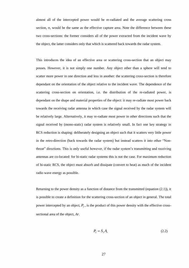
The variation in RCS of a metallic sphere as it increases in size is shown in Figure 2.1 (adapted
from Knott (1993)). The RCS has been normalised to the cross-sectional area of the sphere (the
area of a circle of radius equal to that of the sphere) and the circumference of the sphere has
been normalised to the wavelength. Hence as one moves along the x-axis to the right the
wavelength is decreasing and/or the sphere circumference is increasing.
Figure 2.1 RCS for a metallic sphere
The circumference is given in wavelengths and the RCS is normalised to the
actual cross sectional area of the sphere (this figure has been adapted from
Knott (1993))
The three scattering regimes have been marked in Figure 2.1. It can be seen that the degree of
scattering is small in the low frequency (long wavelength) limit and increases steadily
throughout the Rayleigh regime. When the sphere circumference reaches a wavelength the RCS
levels off and remains at this mean level. Interference between re-radiated creeping waves and

33
waves reflected off the front face gives rises to the interference fringes seen throughout the
resonance region. These fringes become less significant in the optics region where the
wavelength is only a small fraction of the sphere circumference.
2.2.3 Scattering from periodically textured surfaces
As was shown in the previous section, the RCS of a sphere (or an object in general) starts to
become significant when its circumference (or in the case of a more general object its
characteristic dimension) is equal to the wavelength of the incident radiation. Any textured
surface, which has a characteristic dimension that is approximately equal to the wavelength of
the incident radiation, will scatter that radiation significantly.
Surfaces that have random texture will tend to produce random or diffuse scattering: the
incident radiation is dispersed over a range of angles with no particular angle preferred.
Surfaces that have periodic texture (for example a series of grooves of equal width, equally
spaced) scatter radiation into a series of discrete directions. Such surfaces constitute diffraction
gratings and by concentrating the power they re-radiate into beams or orders, they have the
potential to increase the non-specular RCS significantly.
2.2.3.1 The phenomenon of diffraction
According to Huygen's principle, propagating waves, electromagnetic or otherwise can be
visualised as consisting of an infinite number of point sources distributed along the wavefront
(surface of constant phase). Each source emits what are known as secondary wavelets, such that
the wavefront at some later time is the envelope of these wavelets (Hecht (1998)). This concept
is rather oversimplified: if correct, one would observe both forward and backward propagating
waves. The concept was later modified by Fresnel who applied the idea and mathematics of
interference to obviate the need for a backwards propagating wave, and later still by Kirchoff
who demonstrated that it was a direct consequence of the differential wave equation. Thus the
modified Huygens-Fresnel principle, which considers both amplitude and phase, can be applied
to understand the phenomenon of diffraction on a qualitative basis (Hecht (1998)).

34
If a wave encounters an obstacle, either opaque or transparent, which retards the phase or serves
to reduce the amplitude of some segments of the wavefront more than others, then the secondary
wavelets will no longer all be in phase in the forward direction. There will exist other directions
in which the wavelets will interfere in-phase to produce beams or orders and still other
directions in which the wavelets will be completely out of phase and in which there will exist
nulls.
Reflection of a wave from a textured surface has the effect of retarding the phase of some
portions of the wavefront relative to others and hence creates the phase conditions whereupon
constructive and destructive interference can occur. In cases where the wavelength is much
larger than the characteristic dimension of the texture (the Rayleigh regime), the phase shift
created between different segments of the wavefront is only a small fraction of the wavelength
and hence the interference is almost totally constructive.
2.2.3.2 Diffraction gratings
Consider the grating structure shown in Figure 2.2: the surface is textured periodically by slits a
distance g apart, a p-polarised wave (that is one in which the electric field is contained within
the plane of incidence and the magnetic field is transverse to the plane of incidence) is shown,
incident on the grating at an azimuthal angle and incident angle , any diffracted wave occurs
at an angle to the surface normal.

35
(a) (b)
Figure 2.2 A p-polarised wave incident on a grating structure
(a) 3-D projection (b) plan view
In considering the interaction of the incident wave with the grating and the possible creation of
diffracted orders, momentum must be conserved. The momentum, p can be found from the
product of the wavevector 0k with Planck’s constant divided by 2π, :
0kp (2.5)
It transpires that is common to all terms and therefore it cancels, the problem then becomes
one of matching wavevectors.
Begin by considering the momentum parallel to the plane of incidence in the plane of the
grating (the xy plane). The sum of the momentum from the incident wave plus that due to
scattering from the grating, which is equal to an integer multiple, N of the grating vector kg,
must equal to that of the diffracted order, which occurs at an angle to the surface normal and
at an angle to the plane of incidence, hence:
36
cossincossin 00 kNkk g (2.6)
Now consider the in-plane x- and y-components:
gx kkk cossin0 (2.7)
sinsin0kky (2.8)
The total in-plane momentum available, ksum is therefore:
222
yxsum kkk (2.9)
20
2
0
2sinsincossin kNkkk gsum (2.10)
22
00
222sincossin2 kkNkkNk ggsum (2.11)
Real, propagating diffracted orders only occur for 90 , therefore set 90 and
consequently 1sin , and substitute in (2.11):
22
00
222
0 sincossin2 kkNkkNk gg (2.12)
0cossin2sin122
0
22
0 gg kNNkkk (2.13)
This quadratic in k0, (2.13), can be solved to yield the limit frequency at which diffracted orders
will occur for any incident and azimuthal angle and any grating period.
2.3 Surface waves
As stated earlier a surface wave is the microwave analogue of a surface plasmon polariton or
SPP: a localised surface charge density oscillation that can propagate along the boundary
between the metal and the dielectric medium from which the wave was incident (typically air).
37
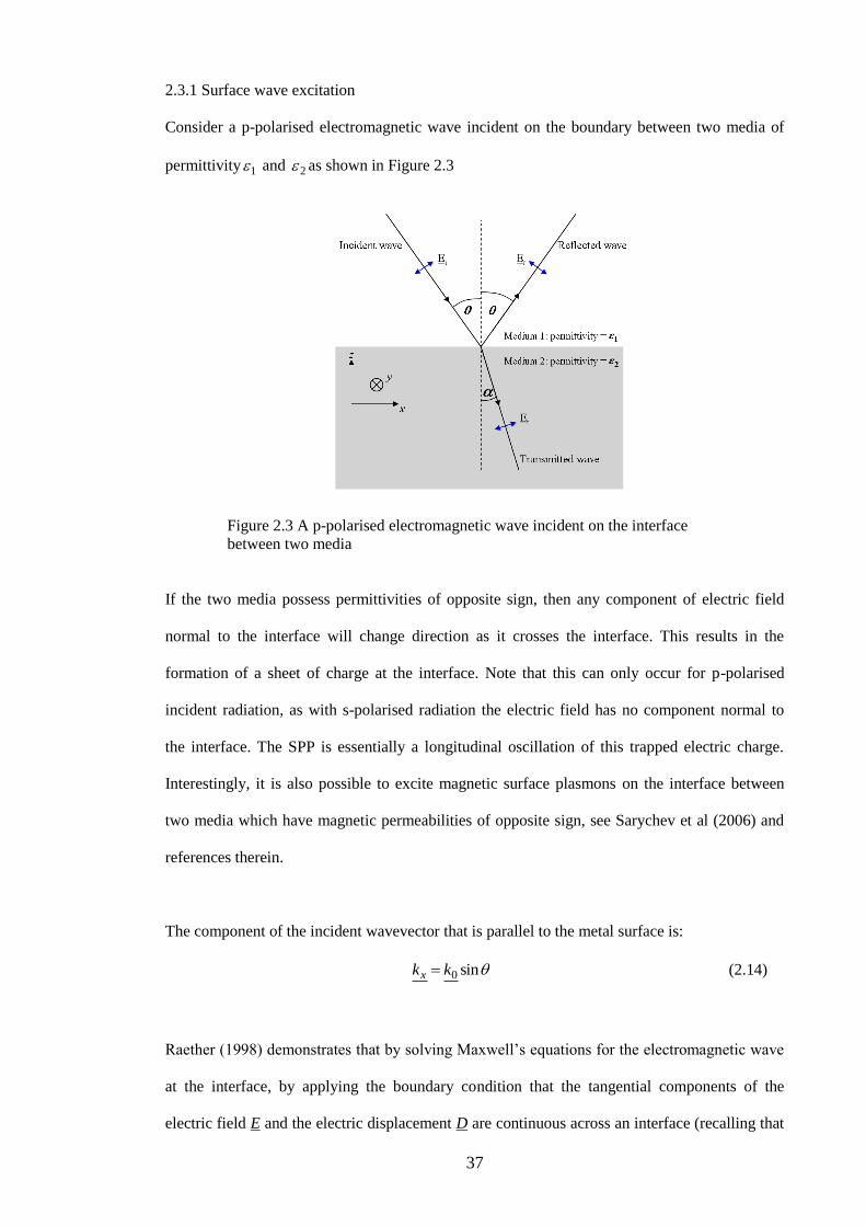
2.3.1 Surface wave excitation
Consider a p-polarised electromagnetic wave incident on the boundary between two media of
permittivity 1 and 2 as shown in Figure 2.3
Figure 2.3 A p-polarised electromagnetic wave incident on the interface
between two media
If the two media possess permittivities of opposite sign, then any component of electric field
normal to the interface will change direction as it crosses the interface. This results in the
formation of a sheet of charge at the interface. Note that this can only occur for p-polarised
incident radiation, as with s-polarised radiation the electric field has no component normal to
the interface. The SPP is essentially a longitudinal oscillation of this trapped electric charge.
Interestingly, it is also possible to excite magnetic surface plasmons on the interface between
two media which have magnetic permeabilities of opposite sign, see Sarychev et al (2006) and
references therein.
The component of the incident wavevector that is parallel to the metal surface is:
sin0kkx (2.14)
Raether (1998) demonstrates that by solving Maxwell’s equations for the electromagnetic wave
at the interface, by applying the boundary condition that the tangential components of the
electric field E and the electric displacement D are continuous across an interface (recalling that

38
the field inside a perfect conductor is everywhere zero) the wavevector of the SPP is given by
(2.15) which is also referred to as the dispersion relation:
2
1
21
21
ckSPP (2.15)
In order excite an SPP, the momentum given by the product of (2.15) with must be supplied.
The form of dispersion relation can be plotted if the frequency dependence of the permittivities
1 and 2 is known. The dispersion of most dielectrics is negligible hence 1 can be considered
to be frequency independent. However, the permittivity of the metal 2 , undergoes huge
changes with frequency, changes which can be described using the Drude free electron model
(Ashcroft (1976)). For a typical metal at 10 GHz the real part of the complex permittivity
around (-104) whilst the imaginary part is around (10
6), by contrast at optical frequencies the
values of the real and imaginary components are typically (-10) and (0.1) respectively. Using
models such as the Drude model allows the dispersion relationship to be plotted.
The dispersion relation (2.15) for the SPP has been plotted in Figure 2.4: the curve describes the
relationship between the wavevector of the surface plasmon and its frequency. Also plotted is
the frequency versus in-plane wavevector for the incident wave – the ―Light line;‖ the constant
of proportionality is the speed of light hence the line is straight with a gradient c.

39
Figure 2.4 Diagramatical representation of the plasmon dispersion relation
In the high frequency limit the frequency of the SPP tends towards the plasmon frequency: at
this frequency the real part of 2 and the real part of 1 are equal in magnitude and opposite in
sign, therefore kSPP is purely imaginary. Close to the plasmon frequency the group and phase
velocities of the mode tend to zero, the SPP is tightly bound to the surface and is described as
being ―plasmon like,‖ its behaviour being predominantly that of a longitudinal oscillation of the
sheet of charge trapped at the interface. By contrast, in the low frequency limit the SPP
frequency tends towards that of the incident wave. This latter limit arises since the behaviour of
the metal very closely resembles that of a perfect conductor, resulting in the dispersion relation
of (2.15) reducing to 1 ckx which is identical to that of the incident radiation, in this
limit the SPP is described as ―photon like,‖ as the SPP is only very loosely bound to the surface.
However, at all frequencies the plasmon momentum is slightly greater than the incident wave
momentum hence some extra momentum is needed in addition to that supplied by the incident
wave, even if the wave is at grazing incidence. This momentum deficit must be satisfied for the
SPP to be excited. A grating which supplies a momentum equal to the product of and the
grating vector kg and can satisfy the deficit:

40
g
gk
2 (2.16)
At microwave frequencies the momentum deficit is very small, at optical frequencies it is much
larger, hence surface plasmons are more easily excited at microwave frequencies than at optical
frequencies. In fact an entire grating is not required: a single ridge, crack or other discontinuity
is all that is required to excite SPPs.
In the microwave regime the conductivity of metals is so high that SPPs can continue to
propagate for distances of hundreds of metres with very little attenuation. This is in stark
contrast to the optical regime where, due the metal having much lower ac conductivity, typical
propagation distances are of the order of microns. On striking a discontinuity such as a gap in a
metal surface, an SPP may be re-radiated and thus contribute to an object’s RCS. Furthermore,
this characteristic permits the design of surfaces which can excite surface plasmons and then re-
radiate them in a tailored manner, for example see the work of Lockyear et al (2004).
2.4 Materials for the absorption of microwave radiation
2.4.1 Underpinning absorption mechanisms
Regardless of the specifics of their design, all absorbing materials rely on the fact that certain
substances absorb energy from electromagnetic waves propagating through them. Materials
which absorb have two components to their refractive index: a real part and an imaginary part,
and it is the imaginary part which accounts for the absorption. The real part is related to the
storage of energy rather than its dissipation as heat, for example the storage of energy in a
capacitor is proportional to the real part of the permittivity of the dielectric between the plates.
The refractive index is related simply to a product the permittivity ( ) and the permeability
( ), and absorption can result from electric loss mechanisms or magnetic loss mechanisms or
both. The loss due to electric effects is analogous to Joule heating of resistance in a circuit,
whereas magnetic losses are generally attributed to the rotation of domains. In either case, the

41
net result is the conversion of energy to heat, this is what is meant by the term loss, or more
formally non-radiative loss, in this context. The degree of absorption exhibited by a particular
structure depends on its configuration in addition to the inherent electromagnetic properties of
its constituent material, although for conversion to heat to occur the refractive index must have
some imaginary component.
It is convenient to deal in terms of the relative permittivity and permeability which are both
expressed as complex numbers as described above:
''' rrr i (2.18)
''' rrr i (2.19)
Note that the permittivity and permeability are relative to those of free space, having values of
8.854 x 10⁻¹²
F/m (to 4.s.f.) and 4 x 10⁻⁷
H/m respectively.
By considering Maxwell’s equations and applying the requisite boundary conditions and
trigonometric identities it can be shown (Grant et al (1995)) that the refractive index n is given
by:
rrn (2.20)
Furthermore the intrinsic impedance Z, of material, is given by:
Z (2.21)
Thus demonstrating that the refractive index has both electric and magnetic components.
In many conventional absorbing materials, a dielectric layer is used over a metal backing.
Consider a wave incident on the boundary between the outer surface of the dielectric and free-
space or air. When the incident wave impinges on the outer surface of the dielectric some
proportion of it is coupled into the dielectric and the remainder is reflected: the proportion that
is reflected determined by the mis-match between the intrinsic impedance of free-space and the

42
input impedance of the material: the greater the difference in impedance the larger the
reflection.
Figure 2.5 Waves incident on a typical absorbing material
The wave coupled into and propagating through the dielectric eventually reaches the metal
backing whereupon it is wholly reflected (assuming a perfect metal) and propagates back
towards the dielectric-air interface. In accordance with reciprocity the same proportion of the
wave energy originally reflected at the outer surface of the dielectric is reflected internally at the
dielectric-air boundary, the remainder couples back into the surrounding air. The wave coupled
back into air then interferes with that initially reflected at the air-dielectric interface.
The internal reflection process within the dielectric is subsequently repeated and the waves
propagating back and forth interfere. If the dielectric is a quarter-wavelength thick, then the
waves reflected from the metal surface will interfere constructively with those internally
reflected at the dielectric-air interface. This situation arises since the metal plate constitutes a
perfect electric reflector and has a reflection coefficient of -1 – the wave suffers a phase change
of radians on reflection and the waves incident on and reflected from the metal will therefore
interfere constructively. Furthermore, since the permittivity of the dielectric is greater than that
of the incident medium (air) the dielectric-air boundary has a positive reflection coefficient: the
waves do not suffer any phase change on reflection from it hence interference between waves
incident on the dielectric-air boundary and those internally reflected is again constructive.

43
Constructive interference results in a standing wave inside the dielectric, the amplitude of which
increases progressively over time as more energy from the incident wave becomes trapped
within the dielectric. If the dielectric is lossy i.e. if the imaginary component of the permittivity
and/or permeability is non-zero, some proportion of the energy of the standing wave is
converted to heat. It can be shown (Grant et al (1995)) that the loss of energy per unit volume
occurs at a rate, DP , given by (2.22):
*.*.Re21 HEikJEPD (2.22)
Where:
E is the electric field strength in V/m
H* is the complex conjugate of the magnetic field strength in A/m
J * is the complex conjugate of the current density in A/m2
From the definition of intrinsic impedance, it is apparent that the value of (2.22) is proportional
to the square of the standing wave amplitude, hence as the wave amplitude increases so does the
rate of loss. Eventually a point is reached where the rate of loss is equal to that at which energy
from the incident wave is coupling into the dielectric – the standing wave amplitude reaches a
steady state.
The amplitude of the wave re-emitted from the dielectric back into air depends on the
impedance mis-match at the dielectric-air interface and also on the standing wave amplitude:
enhancement of the standing wave amplitude results in the amplitude of the re-emitted wave
also increasing. This in turn affects the resulting interference between the re-emitted wave and
the wave initially reflected at the air-dielectric interface. If the amplitudes of these two waves
are equal then they may interfere destructively, hence the net radiation from the material or
rather its reflectivity will be zero. This is the mechanism underpinning the operation of all
resonant absorbers.

44
If the material properties of the dielectric are such that the amplitude of the initially reflected
wave is too high, or the steady state amplitude of the standing wave is too low, then although
there will be destructive interference the net reflectivity will not be zero. Conversely, if the
amplitude of the re-emitted wave is higher than that of the initially reflected wave then the net
reflectivity will not be zero. For the reflectivity to be zero then radiative loss (re-emitted wave
amplitude) must equal the non-radiative loss (the absorption by the dielectric).
2.4.2 Conventional absorbing materials
Examples of resonant absorbing materials that can be described as above include Salisbury
screens (Salisbury (1952)) and Dallenbach layers (Ruck (1970)). The latter structure is as
described above and shown in Figure 2.5. Shown in Figure 2.6 is a plot of the reflectivity of a
hypothetical Dallenbach layer for a p-polarised wave incident over a range of angles, as
simulated using the finite element model to be detailed in the next chapter. In this case the
dielectric material was non-magnetic 01 ir , with permittivity 4.04 ir and 3.75 mm
thick.
Figure 2.6 Plot of the simulated reflectivity of a Dallenbach layer for a p-
polarised wave at different angles of incidence
For normal incidence the resonance is just above 10 GHz a consequence of the quarter-
wavelength condition detailed above. Minimum reflectivity is –22 dB indicating a close match

45
between the radiative and non-radiative losses. As the incident angle is increased the resonance
becomes shallower and shifts to higher frequencies. Note that the minimum thickness of a
Dallenbach is a quarter-wavelength at the frequency of interest allowing for the refractive index
of the core. This restriction can be of significant inconvenience and is not encountered with the
ultra thin absorbers which are the focus of this thesis.
The Salisbury screen consists of a very thin lossy layer spaced a quarter-wavelength from a
metal backing typically by a low loss material such as air or foam. The conventional approach
to designing a Salisbury screen is to consider the structure as a quarter-wave section of
transmission line and then adjust the surface impedance of the thin lossy layer until the input
impedance of the structure matches that of free-space. However, since this structure constitutes
a resonant absorber it can also be thought about in the terms described above. A diagram of a
typical Salisbury screen Shown in Figure 2.7, along with the corresponding reflectivity spectra
as simulated using the finite element model.
Again the resonance occurs close to 10 GHz for normal incidence due to the spacing of the
lossy layer above the ground plane being a quarter-wave wavelength. It is clear that the
performance of the Salisbury screen is highly sensitive to incident angle with a frequency shift
of 4 GHz occurring between normal incidence and 45° incidence. Note that the measured
physical thickness of the Salisbury screen is double that of the Dallenbach layer due to the
former using air as a dielectric.

46
(a)
(b)
Figure 2.7 A typical Salisbury screen
(a) geometry (b) simulated reflectivity for a p-polarised wave over a range of
incident angles
In order to increase the absorption bandwidth of a Salisbury screen, a multiplicity of thin lossy
layers can be used instead of just one: such a structure is referred to as a Jaumann absorber
(Conolly (1977)). Each lossy layer is typically spaced a quarter-wavelength from the adjacent
lossy layers thus increasing the overall thickness of the structure by a factor of n if there are n
layers. As will be demonstrated later in this thesis, increasing absorption bandwidth beyond a

47
certain point cannot be achieved without proportional increases in overall thickness, this is true
for all types of absorber, irrespective of their geometry.
2.5 Current research in electromagnetic materials
Research concerning the interaction of electromagnetic radiation and patterned metal surfaces
has produced a series of extraordinary and unexpected breakthroughs in recent years. The
pioneering work of Ebbesen et al (1998) has revealed that two-dimensional arrays of cylindrical
holes in a thin metal film can support the transmission of more radiation that is directly incident
on the apertures themselves. This phenomenon can be explained in terms of the excitation of
surface plasmon polaritons on the metal surface, the frequency of which is determined by the
hole spacing in accordance with momentum conservation as detailed above.
Others, such as Suckling et al (2007) have corroborated these findings and have extended the
work to consider hexagonally symmetric hole arrays to create azimuthally-independent surface-
plasmon mediated transmissive structures. Yang (2008) demonstrated that the SPP dispersion
curve can be tailored by altering the geometry of the hole arrays. Specifically, Yang (2008)
demonstrates that the size of the holes in a transmissive structure can be modified in order to
alter the plasma frequency and asserts that rectangular holes result in more tightly bound
plasmons than otherwise equivalent arrays of circular holes. Others including Pendry (2004)
have termed these tightly bound surface waves as ―Spoof‖ surface plasmons since their
dispersion can be manipulated through changes to structure rather than to constituent material
properties.
This type of structure has evolved into much thinner forms via the work of Sievenpiper (1999)
who analysed a ―mushroom‖ structure: an array of hexagonal metal patches connected to a
ground plane using vias. Using a circuit model, Sievenpiper demonstrates that this structure
supports propagating TM surface modes below its resonance frequency and TE modes above its
resonant frequency. Lockyear (2009) exploited prism coupling to experimentally determine the

48
dispersion of a Sievenpiper mushroom structure that was only 0.8 mm thick despite operating at
frequencies around 20 GHz or 15 mm free-space wavelength.
The ability to tailor the response of this class of metamaterial has been demonstrated
numerically by Navarro-Cia et al (2009). Navarro-cia presents numerical results for split-ring
resonator structures and demonstrates their capacity to excite broadband surface plasmons, and
hence overcome many of the problems associated with the preceding structures. Navarro-cia
also demonstrates that these split ring structures can be applied to create a planar waveguide for
the guiding of spoof plasmons.
The challenge of creating absorbing materials which are much thinner and exhibit greater
stability under azimuthal and incident angle variations than those used conventionally is the
primary focus of this thesis. However others have also pursued similar goals including Lockyear
(2003) who realised the use of a dual-period bi-grating structure for the excitation of surface
plasmon modes which are highly independent of incident and azimuthal angle. Although these
structures are much thicker than the absorbing materials considered herein, they still afford
significant reductions in reflectivity by virtue of dielectric losses in the material used to fill the
grating grooves. The same author has also recently published work (2009) pertaining to an
absorbing structure formed from an array of discs, which operate via a similar principle to the
structures considered in this thesis. This structure combines the advantages of being very thin
(total thickness approximately 1% of the operating wavelength) and producing absorption which
is largely independent of incident and azimuthal angles and polarisation state.
Others including Zhang (2003), Sievenpiper ((1999) and (2003)) and Gao (2005) considered
metal-dielectric-metal laminates into the upper metal layer of which are cut two mutually
orthogonal sets of sub-wavelength slits, and thus dividing the upper metal layer into an array of
square patches. These bi-grating structures are capable of guiding electromagnetic waves and
therefore have myriad applications in communications and electronics. Zhang et al (2003)
analyzed such a square patch array as a perfect magnetic conductor (see Sievenpiper (1999))

49
and using a transmission line model applied the structure to suppress side lobes from an antenna
array. Zhang also presents normal incidence reflectivity data for this structure but does not
present a study of its angle or polarisation dependence.
Work by Sievenpiper et al (2003) involved the introduction of varactor diodes to a square patch
array similar to that used by Zhang (2003) but with vias between the centre of the patches and
the lower metal plane. The diodes were connected between adjacent patches and the application
of a bias voltage across them alters the phase of the reflected waves thus creating an electrically
tuned device for use in beam-steering that can also be used as an absorber (Gao (2005)).
Other approaches include those of Tennant and Chambers, (2004) who created a hybrid
Salisbury screen type absorber in which, in place of the conventional resistive layer, was used a
frequency selective surface (FSS). The FSS consisted of small dipole-like elements at the centre
of which was connected a PIN diode. Varying the diode bias current permits resistive tuning of
the structure and hence allows the structure’s reflectivity to be varied. In this case the overall
structure thickness was less than 5 mm despite being formed using a spacer with permittivity
very close to that of air. Significant reductions in reflectivity were measured between 8 GHz and
14 GHz, therefore, whilst being substantially thicker than the structures considered in this
thesis, this hybrid absorber is thinner than a conventional Salisbury screen.
2.6 Important applications for absorbing materials
Historically, the primary application for absorbing materials has been in reducing the RCS of
military vehicles. Whilst the military demand remains, the advent of mobile communications
and wireless networking has resulted in a huge growth in the number of radio frequency
transmissions across many frequency bands. This has in turn led to a requirement to ―clean-up‖
the radio frequency environment and to be able to screen-out specific signals and frequencies.
Materials which can selectively absorb and transmit radio frequency radiation, whilst being low
cost and low profile are therefore increasingly in demand in commercial applications.
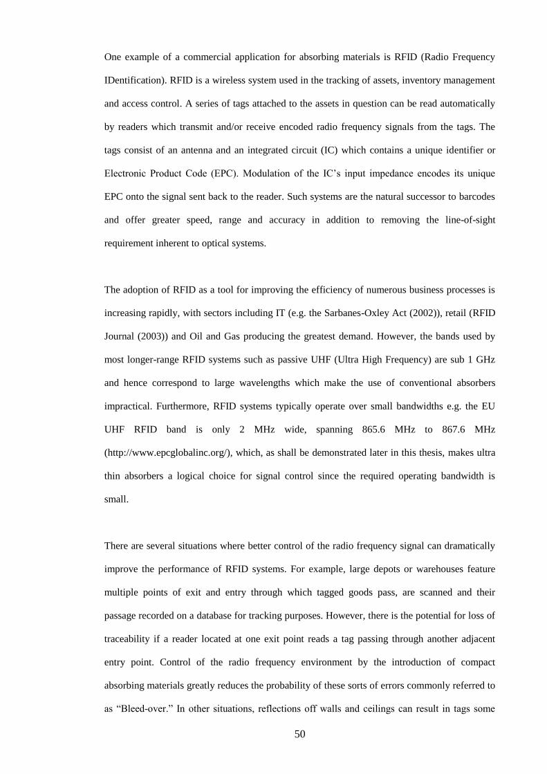
50
One example of a commercial application for absorbing materials is RFID (Radio Frequency
IDentification). RFID is a wireless system used in the tracking of assets, inventory management
and access control. A series of tags attached to the assets in question can be read automatically
by readers which transmit and/or receive encoded radio frequency signals from the tags. The
tags consist of an antenna and an integrated circuit (IC) which contains a unique identifier or
Electronic Product Code (EPC). Modulation of the IC’s input impedance encodes its unique
EPC onto the signal sent back to the reader. Such systems are the natural successor to barcodes
and offer greater speed, range and accuracy in addition to removing the line-of-sight
requirement inherent to optical systems.
The adoption of RFID as a tool for improving the efficiency of numerous business processes is
increasing rapidly, with sectors including IT (e.g. the Sarbanes-Oxley Act (2002)), retail (RFID
Journal (2003)) and Oil and Gas producing the greatest demand. However, the bands used by
most longer-range RFID systems such as passive UHF (Ultra High Frequency) are sub 1 GHz
and hence correspond to large wavelengths which make the use of conventional absorbers
impractical. Furthermore, RFID systems typically operate over small bandwidths e.g. the EU
UHF RFID band is only 2 MHz wide, spanning 865.6 MHz to 867.6 MHz
(http://www.epcglobalinc.org/), which, as shall be demonstrated later in this thesis, makes ultra
thin absorbers a logical choice for signal control since the required operating bandwidth is
small.
There are several situations where better control of the radio frequency signal can dramatically
improve the performance of RFID systems. For example, large depots or warehouses feature
multiple points of exit and entry through which tagged goods pass, are scanned and their
passage recorded on a database for tracking purposes. However, there is the potential for loss of
traceability if a reader located at one exit point reads a tag passing through another adjacent
entry point. Control of the radio frequency environment by the introduction of compact
absorbing materials greatly reduces the probability of these sorts of errors commonly referred to
as ―Bleed-over.‖ In other situations, reflections off walls and ceilings can result in tags some

51
distance from the exit point being read spuriously – the database will then record them as
having passed out of the warehouse when in fact they have not. Again the application of low-
profile absorbing material provides a cost efficient, unobtrusive solution.
Another important application for absorbing materials is the field of renewable energy
generation. The widespread deployment of wind turbines has hitherto been impeded by the large
RCS such structures present to both civilian and military radar systems (Tennant and Chamber
(2006)). Furthermore the ability to distinguish between moving aircraft and static objects by
using Doppler filtering is negated since the tip of the turbines can easily achieve speeds of 100
miles per hour. This has precluded the development of many otherwise preferred potential wind
farm sites due to their proximity to airports. The application of absorbing material can
significantly reduce the RCS of wind turbines and affords much greater freedom in the location
of wind farms.
The explosive growth of wireless networks and mobile telecommunications over the past
decade, has created a desire to control the radio frequency environment within buildings. For
example, a study by Houliston et al (2009) revealed that RFID systems have the potential to
cause significant interference with drug infusion equipment in hospital environments. Another
study by Butterworth et al (1997) considered the propagation of radio frequency signals within a
building in relation to the use of a mobile communication system. In both cases there is the
potential to apply thin materials which selectively absorb and/or transmit to either screen out
unwanted signals or to reduce problems arising from reflections and interference. Selective
transmission and absorption of particular frequencies can be applied to prevent the use of
cellular phones whilst permitting the use emergency TETRA band radio. A similar requirement
exists in the creation of ―Quiet zones‖ in public places such as on trains, where the ability to
continue to use TETRA band frequencies is paramount. Thin absorbing and transmitting
materials such as those detailed in this thesis are of particular value in these situations.
Conventional frequency selective screens (Munk (2000)) could also be applied in this instance

52
but might not afford the same degree of frequency selectivity, without requiring multiple layers
and hence increased thickness.

53
Chapter 3
Modelling
3.1 Introduction
The theoretical results presented in this thesis have been produced using Ansys’s High
Frequency Structure Simulator (HFSS) software. HFSS is a finite element code that can be
applied to simulate the electromagnetic behaviour of various systems from antennas, to radar
absorbers, frequency selective screens and even complex PCB geometries. In this chapter the
basis of the finite element method is described and the manner in which HFSS is used to
simulate the behaviour of the microcavity arrays is presented. Some of the work in this chapter
has been adapted from Huebner (2001) and Zienkiewicz et al (2005), the HFSS user manually
has been used extensively to provide information specific to HFSS.
3.2 The finite element approach
According to Huebner (2001), Finite element analysis is a numerical method of finding
approximate solutions to partial differential equations, such as Maxwell’s equations. The
method consists of dividing the problem geometry into a series of small elements which
combine together to form a mesh representing the entire structure.
Finite element analysis can be applied across a diverse range of problems in physics and
engineering including: fluid dynamics, mechanical vibrations and stress, thermodynamics and
electromagnetism. In each of these cases the governing equations and boundary conditions are
generally well-known but very often the geometries under consideration are arbitrary or feature
irregularities, thus precluding analytical solutions. Furthermore, when considering the behaviour
of a field quantity within a continuous body, there are an infinite number of unknowns since the
field quantity can possess any number of values at each generic point within the body (Huebner
(2001)).

54
These problems can be transformed into ones of finite unknowns by dividing the geometry into
a series of elements within each of which the unknown field quantity is expressed as an
approximating function, the form of which is assumed. The approximating functions are defined
in terms of the values of the field quantities at specific points or nodes. Nodes lie either on the
boundaries between adjacent elements or within an element. Hence the nodal field values and
the approximation functions define the behaviour of the field quantity within an element. In
finite element analysis the nodal values are the unknowns and once found the approximation
functions then describe the behaviour of the field quantity throughout the entire geometry, this
is the essence of the finite element method (Zienkiewicz et al (2005)).
Within HFSS the mesh elements take the form of tetrahedra, and the field quantities of interest
are the electric and magnetic fields. The accuracy of the HFSS solution depends on the size of
the elements with smaller elements producing more accurate answers. However, the smaller the
average element size the greater the number of elements that is needed to represent the entire
structure and hence the larger the computational resource needed to solve the problem. HFSS
deals with the compromise between problem size and accuracy by using an iterative method in
which the element size is progressively reduced and hence problem size and accuracy
progressively increased. The solution resulting from each successive iteration is compared to
that from the previous iteration. Once the difference in successive solutions is sufficiently small
one can be confident that any further refinements to the mesh are superfluous and the solution is
said to have converged. Typically, a convergence criterion equivalent to a change in the solution
of less than 1% is applied.
3.3 An overview of HFSS
3.3.1 Assembling the structure to be simulated
Within HFSS there exists a CAD program which allows the user to assemble the structure to be
simulated by using a number of commands for the construction, to-scale, of one-, two- and three
dimensional objects. For regular forms such as cuboids and cylinders there exist integral
drawing commands where the user simply specifies the location of one corner of a cuboid for
55
example, then enters its x-, y- and z-dimensions. For more complex and/or irregular shapes, the
user must execute a series of drawing commands in a certain sequence in order to form the
desired geometry. Such commands might include rotating objects, mirroring an object about a
plane, splitting objects or creating a surface from the intersection of two object faces. Such a
surface can then be rotated about an axis or swept along a vector in order to create a three-
dimensional object. There exist myriad combinations of these commands such that almost any
desired structure can be assembled. The series of drawing commands that have been executed
by the user are stored within HFSS but can be modified retrospectively as required, for example
one may wish to change the radius of a sphere or the location of a plane.
3.3.2 Assigning material properties
When initially created, each three-dimensional object is automatically assigned to have the
electromagnetic properties of vacuum by default. Two-dimensional objects are defined in terms
of a boundary condition rather than a material property as will be described later. The material
properties of a three-dimensional object can be assigned in terms of a number of quantities
including:
o Relative permittivity – the real component, 'r and dielectric loss tangent ''' rr
where ''r is the imaginary component, are specified
o Relative permeability – the real component, 'r and magnetic loss tangent ''' rr
where ''r is the imaginary component, are specified
o Bulk conductivity in Siemens/metre
The user may themselves enter the values of the requisite quantities or they may choose from an
integral database which lists typical values for well-known materials. Furthermore, it is possible
to represent anisotropic materials by entering values corresponding to those in the three
Cartesian axial directions. The frequency dependency of materials can also be considered by

56
either entering the known quantity values at specific frequencies or by using integral fitting
models including: linear, Debye and Djordjevic-Sarkar (Hall et al (2009)).
Within HFSS, metal objects that have high but finite conductivity are represented by a surface
approximation: the field solution is generated only at the surface of the metal not within its
volume. This finite conductivity boundary approach reflects the fact that metals are imperfect
conductors – they are to some extent, lossy. At the surface of these imperfect conductors the
following boundary condition applies:
tan
tan
H
EZ s (3.1)
Where:
Etan is the component of the electric field tangential to the boundary or surface
Htan is the component of the magnetic field tangential to the boundary or surface
ZS is the surface impedance
In cases where the thickness of the metal is much larger than a skin depth, the surface
impedance can be found from equation (3.2):
2
1
21
jjZs (3.2)
Where:
is the angular frequency of the excitation,
is the conductivity of the metal,
is the permeability of the metal
And:
2
(3.3)
This approach is only valid if the metal’s thickness is significantly greater than the skin depth at
the solution frequency. If this condition is not met then it is necessary to apply what is termed a
layered impedance boundary. A layered impedance boundary represents the thin metal layer as a

57
two-dimensional surface which has a complex impedance resulting from the intrinsic properties
of the material in question (typically copper for the models used in this thesis) and its thickness.
The user is required to select the surface in question, its constituent materials an also enter a
value for surface roughness, h: the root-mean-square deviation of the surface of the metal from a
plane.
The greater the surface roughness the lower the conductivity. HFSS uses the following formula
to modify the conductivity to allow for roughness:
2
w
cK
(3.4)
Where:
c is the modified conductivity
And:
6.1
2exp1
hKw
(3.5)
And all other terms have the meanings given above.
Using the user-defined thickness, conductivity and roughness, HFSS is then able to calculate the
complex surface impedance using analytical formulae which are not detailed in the user manual.
3.3.3 Boundary conditions
The behaviour of the electromagnetic fields at the surfaces of the user-defined geometry and at
the interfaces between objects are specified by one of the following boundary conditions:
o Layered impedance
o Perfect E
o Perfect H
o Radiation
o PML

58
o Finite conductivity
o Symmetry
o Master and Slave
o Lumped RLC
Layered impedance boundaries have been detailed above. A perfect E boundary represents a
surface which is perfectly conducting: the component of electric field tangential to the surface is
zero hence the electric field is normal to the surface. A perfect H boundary is one across which
the tangential component of H is continuous. For surfaces internal to the model this represents a
boundary that is ―natural,‖ and the field propagates through with no distortion. For external
model surfaces this boundary condition simulates a perfect magnetic conductor: one on which
the tangential component of the H-field is zero.
In situations where the geometry being simulated radiates or re-radiates, HFSS applies a
radiation boundary condition to truncate what would otherwise be an unbounded problem. This
boundary condition is designed to remove the radiated energy from the model but without
causing any unphysical reflection that would distort the solution. There are two types of
radiation boundary condition that HFSS applies: absorbing boundary conditions (ABCs) and
perfectly matched layers (PMLs).
ABCs can only absorb waves which are incident normal or near-normal to the boundary surface:
whilst there is no strict definition, in this case near-normal would generally mean angles up to
approximately 20°. Furthermore ABCs must be spaced at least a quarter-wavelength away from
radiating structures. These restrictions arise because the ABC is an approximate boundary
condition the accuracy of which decreases rapidly as the distance between it an any radiating
structure decreases to less than a quarter wavelength.
PMLs are three-dimensional structures which consist of artificial materials, the properties of
which are automatically tailored by HFSS such that waves incident upon them are wholly

59
coupled into the PML with minimal reflections. The permittivities and permeabilities of the
PML are complex and anisotropic in order to provide material which is absorbing and which has
an intrinsic impedance matched to that of free-space i.e. the relative permittivity and
permeability are equal, hence the term perfectly matched layer. In contrast to an ABC, a PML
can absorb waves incident over a wide range of angles and can therefore be applied to problems
in which waves are incident on a surface at angles significantly off-normal. The disadvantage of
PMLs is that they require greater computational resource than do ABCs.
Finite conductivity boundaries are automatically applied to the faces of three-dimensional
objects which are assigned the properties of a metal but can also be applied to two-dimensional
surfaces. A description of the finite conductivity boundary condition has been given above.
A symmetry boundary can be applied to exploit a plane of electromagnetic symmetry which a
problem geometry possesses. Using a symmetry boundary condition allows only half or, if two
symmetry boundaries are applied a quarter, of the problem geometry to be modelled and the
solution can be mirrored about the plane or planes to produce the solution for the entire object.
This approach has the advantage of significantly reducing the required computational resource
without compromising the accuracy of the solution.
Periodic boundary conditions, also known as master and slave pairs, can be applied to periodic
structures in order to represent an infinite array of unit cells whilst only drawing and solving the
field equations for one unit cell. These boundary conditions force the electric field on the slave
boundary to be identical to that on the master boundary to within a phase difference. This type
of boundary condition has been used extensively throughout this thesis and is detailed with
reference to microcavity arrays in the next section.
A lumped RLC boundary can be applied to designate a surface as having a certain resistance
and/or inductance and/or capacitance. This type of boundary is often applied to model problem

60
geometries which include circuit components e.g. RFID tags. This boundary condition has not
been used within models presented this thesis.
3.3.4 Excitations
Within HFSS there exist several methods for exciting i.e. injecting electromagnetic energy into,
the structure. These include:
o Wave ports
o Lumped ports
o Incident waves
o Voltage sources
o Current sources
o Magnetic bias
Wave ports are two-dimensional objects applied to an external face of a problem geometry that
represent a cross-section through a waveguide. The problem geometry is therefore excited by
the modes naturally supported by such a waveguide. Wave ports can only be applied to external
faces in contrast to lumped ports which can be applied to faces internal to the modelled
geometry. Lumped ports also feature a reference impedance that is defined by the user. Note
that neither wave nor lumped ports have been used in models presented in this thesis.
Incident wave excitations have been used exclusively throughout this thesis and consist of
sinusoidal radiation incident upon the problem geometry. Within HFSS it is possible to define
the form of the incident wave as being plane or cylindrical, and to define the wave as being
evanescent if desired. An evanescent wave is a plane wave but one whose amplitude decays
with distance in the propagation direction.
Throughout the models presented in this thesis, plane incident wave excitations have been used
to excite the microcavity array structures. The angles of incidence and azimuth can all be
tailored as required by entering the appropriate values for the propagation vector in spherical

61
polar co-ordinates. The polarisation state can be varied from TE to TM or the electric field
vector can be orientated at any angle between these two extremes.
3.3.5 Meshing
After the model geometry has been input, material properties specified, boundaries and
excitations applied, the solution process begins with the generation of what is termed the initial
mesh. This coarse mesh of tetrahedral elements then undergoes optional ―lambda refinement,‖
whereby the maximum tetrahedral size is reduced to a user-defined fraction of a wavelength,
typically 0.33. This ensures a basic level of resolution taking into account the materials used
within the model. HFSS then uses this mesh to create an initial field solution at a frequency
specified by the user. Typically, an initial mesh contains between 500 and 2000 elements.
The objective of the mesh refinement process is to create an array of elements each of which is
small enough to represent the field accurately but not so large that the overall problem size
becomes prohibitive. The required tetrahedral size is determined locally by selectively refining
the mesh in accordance with the field gradient: in areas of high field gradient the tetrahedral size
must be smaller in order to accurately represent the field. The generation of the initial mesh
allows these high error density areas to be identified and they become the initial focus of the
mesh refinement.
The refinement of the mesh is monitored by comparing the solution it yields to that yielded by
the previous mesh iteration. As the tetrahedral size decreases the level of detail increases,
eventually a point is reached where the mesh affords sufficient detail and further decreases in
tetrahedral size serve only to increase the computational resource required. At this point the
solution is said to have converged and the mesh refinement process stops. Typically, the
criterion for the refinement process to be stopped is a change in the field solution between
successive iterations of less than 1%. For the microcavity array structures considered in this
thesis, convergence typically occurs once the mesh contains 30, 000 to 40, 000 elements. Such a
model might take
62
The figure below contains images of typical initial and final meshes. In this case the structure
being simulated is a mono-grating type microcavity array with the slit located at the centre of
the unit cell. The metal layers are shown by the thick black lines added to the 2-D elevations;
Figures 3.1(b) and (d). The decrease in the size and increase in the number of tetrahedra is
readily visible.
(a) (b)
(c) (d)
Figure 3.1 Plots of typical finite element meshes constructed using HFSS
(a) 3-D projection of the initial mesh for a typical microcavity structure, 1258
tetrahedra (b) cropped 2-D side elevation of the initial mesh for a typical
microcavity structure, 1258 tetrahedra (c) 3-D projection of the final mesh for
typical microcavity structure 43401 tetrahedra (d) cropped 2-D side elevation
of the final mesh for typical microcavity structure 43401 tetrahedra

63
Once solution convergence has been realised a frequency sweep can begin. Rather than create a
new mesh HFSS uses the last mesh created during the refinement process during the frequency
sweep. There is an assumption that this mesh is sufficient to produce accurate solutions across a
range of frequencies. However, this assumption is validated by the results in later sections.
Furthermore, by meshing or re-meshing at the resonant frequency of the structure the highest
field gradients will already have been encountered and accommodated by the time other
frequencies, including higher frequencies, are simulated. The total run time for a model
including meshing, convergence and a frequency sweep is typically between four and eight
hours depending on the number of points required to accurately describe the resonant modes
present.
The above process can be set-up to run automatically and the user will often not need any
knowledge of the detailed form of the mesh. However, in certain circumstances it is
advantageous to instruct HFSS to create a finer mesh in specific areas of interest. For example
when considering the detailed behaviour of the field in the vicinity of a sub-wavelength
aperture, a very fine mesh might be required such that the field plots have sufficient detail.
The process of manually creating regions of finer mesh is known as seeding. Seeding can be
done one object at a time by specifying the maximum length of the tetrahedra within the object.
However, in some cases an even finer level of control over the mesh is required and the use of
what are known as virtual objects is required. A virtual object is a small object drawn entirely
inside a larger object and has identical material properties to the larger object. The virtual object
is located where the greater level of detail is required and it alone is seeded as required. This
leaves the majority of the volume of the larger object with a coarser mesh and thus uses less
computational resource than seeding the whole object would require.

64
3.3.6 Post-processing
The field solution produced by HFSS can be used to determine many of the electromagnetic
characteristics of the problem geometry. For the microcavity array structures considered in this
thesis, the focus is on determining the reflectivity and transmissivity, however other
characteristics such as the near field and far field radiation pattern can also be studied. In order
to understand the interaction of microwaves with the microcavity arrays, the electric and
magnetic fields of the resonant modes supported can be plotted and studied in three dimensions
and can be animated with respect to phase, frequency and position.
The HFSS fields formulation divides the problem into three sources: incident fields, total fields
and scattered fields. The incident field is that arising from the incident wave as defined by the
user. The total field is that which exists by virtue of the incident field and its interaction with the
structure in question: it is the total field that the HFSS field solution determines. The scattered
field is determined from the difference between the incident and total fields. To illustrate this
approach, consider the following example.
Consider a model of a metal plate, infinite in extent within the xy plane and that is several tens
of skin depths in thickness in the z-direction. In a laboratory measurement, a wave incident on
the surface of this plate in the z-direction would be near-perfectly reflected; there would be no
transmission of the wave through the plate. Within HFSS the incident field is simply the wave
incident on the plate, but the manner in which HFSS is formulated places this exciting field
everywhere within the model. Therefore, even though there can be no transmission of the field
through the plate, the incident field does exist in both half spaces – both above and below the
plate.
The total field is the actual field solution that would exist above and below the plate in a
laboratory measurement. So, below the plate the total field is zero and above the plate the total
field is the superposition of the incident wave and that reflected from the metal plate. The
scattered field is determined by subtracting the total field from the incident field, allowing for
65
both amplitude and phase. In the upper half-space this corresponds to the wave reflected from
the metal plate – but only the reflected component. Intuitively one might expect the scattered
field in the lower half-space to be zero since no energy can propagate through the plate.
However, the scattered field amplitude in the lower half-space is high-valued, but the wave is in
anti-phase with the incident field in this region. This results in destructive interference and the
net amplitude (i.e. total field) in the lower half-space is zero – as expected.
The above description can be applied to structures which do transmit radiation. In such cases the
total fields can be used to find the fractional transmission coefficient whilst scattered fields must
be selected to find the fractional reflection coefficient. In both cases the time-averaged Poynting
vector must be integrated over a plane which cuts through the model. The ratio of this
calculation for scattered fields to that for incident fields yields the reflection coefficient when
performed over a plane located in the upper half-space. Similarly, total fields yields the
transmission coefficient when the total fields calculation is performed over a plane in the lower
half-space.
3.4 Modelling approaches used in this thesis
3.4.1 Mono-grating reflection structures
Chapter 4 details the angle- and polarisation-dependant reflectivity of microcavity array
structures in which only one of the two metal layers is perforated by sub-wavelength slits. The
total thickness of these structures is less than 1% of their operating wavelength and the width of
the slits is of the same order of magnitude. These structures support resonant modes which
exhibit field strengths around 100 times greater than those of the incident wave. These factors
combine to produce very high field gradients and consequently a dense finite element mesh.
The metal and dielectric layers were formed from cuboids drawn using the HFSS primitive
object commands. The metal layers were designated as copper with a conductivity of 5.8. 107
S/m as obtained from the HFSS materials database. The permittivity of the FR4 core was set to
(4.17 +i0.07) in accordance with analysis of free-space analysis of a plain FR4 sheet using the
focused horn apparatus as detailed in Chapter 4.

66
One period of the structure in the y-direction (a length of 10 mm) was drawn using the HFSS
user interface with an infinite array of these unit cells being modelled by application of periodic
boundary conditions. The x-dimension was set to 4 mm and the application of a second set of
periodic boundary conditions resulted in an infinite array in both x- and y-directions being
modelled. The sub-wavelength slit was located at the centre of the unit cell between y = 4.85
mm and 5.15 mm, thus it has a width of 0.3 mm. In later models the effect of altering the slit
width and the dielectric core thickness were investigated. These dimensions are easily
manipulated in the model using the same commands as were used to draw the model described
above. However, every time a dimension of material property is changed, the solution must be
generated again from the beginning.
(a) (b)
Figure 3.2 Mono-grating structure as modelled in HFSS
(a) Selected Dimensions and materials (b) Boundary conditions
Above the microcavity structure a box designated as vacuum was added. This box was 40 mm
high – approximately one wavelength at the fundamental resonant frequency. Whilst this is

67
larger in the z-dimension than is generally regarded to be adequate, experience has
demonstrated that a larger vacuum box produces more accurate values when integrating the
Poynting vector over the plane located as shown: if the plane was closer to the surface of the
microcavity array, then the integration may include reactive field components rather than just
those of the propagating reflected wave.
To the top of the vacuum box was added the PML, the thickness of which was set to 7.5 mm.
The top face of the PML was not explicitly assigned any boundary condition, therefore HFSS
assigns it a perfect E condition by default. Again 7.5 mm is thicker than the minimum value the
HFSS PML macro recommends, but experience demonstrates that a greater thickness produces
more accurate solutions, particularly at higher incident angles. This is due to the anisotropy of
the PML: the imaginary permittivity and permeability are much greater in the z-direction than
the x- and y-directions, hence the wave amplitude decreases much more rapidly in the z-
direction than the other two directions. However, as the incident angle is increased from 0° the
specular reflected wave propagates through the PML at angle to the z-direction, hence the rate
of attenuation with distance in the z-direction is diminished. A thicker PML is therefore
required in order to ensure that total attenuation is sufficient to eliminate any reflections.
Models were run at incident angles of 16° and 57.4° to allow comparison with experimental
data. Models were meshed at the resonant frequency of the fundamental model: 7.1 GHz in this
case. The initial mesh had approximately 1, 300 tetrahedral elements and after 20 iterations this
had increased to approximately 32, 000, by which point the variation in the solution between
iterations was approximately 0.6%. The final mesh has been plotted in the figure below. It can
be seen that the typical element size is much less in the core and in particular around the slit
than it is in the vacuum box above the microcavity structure. This demonstrates the selective
nature of the mesh refinement process as described above.
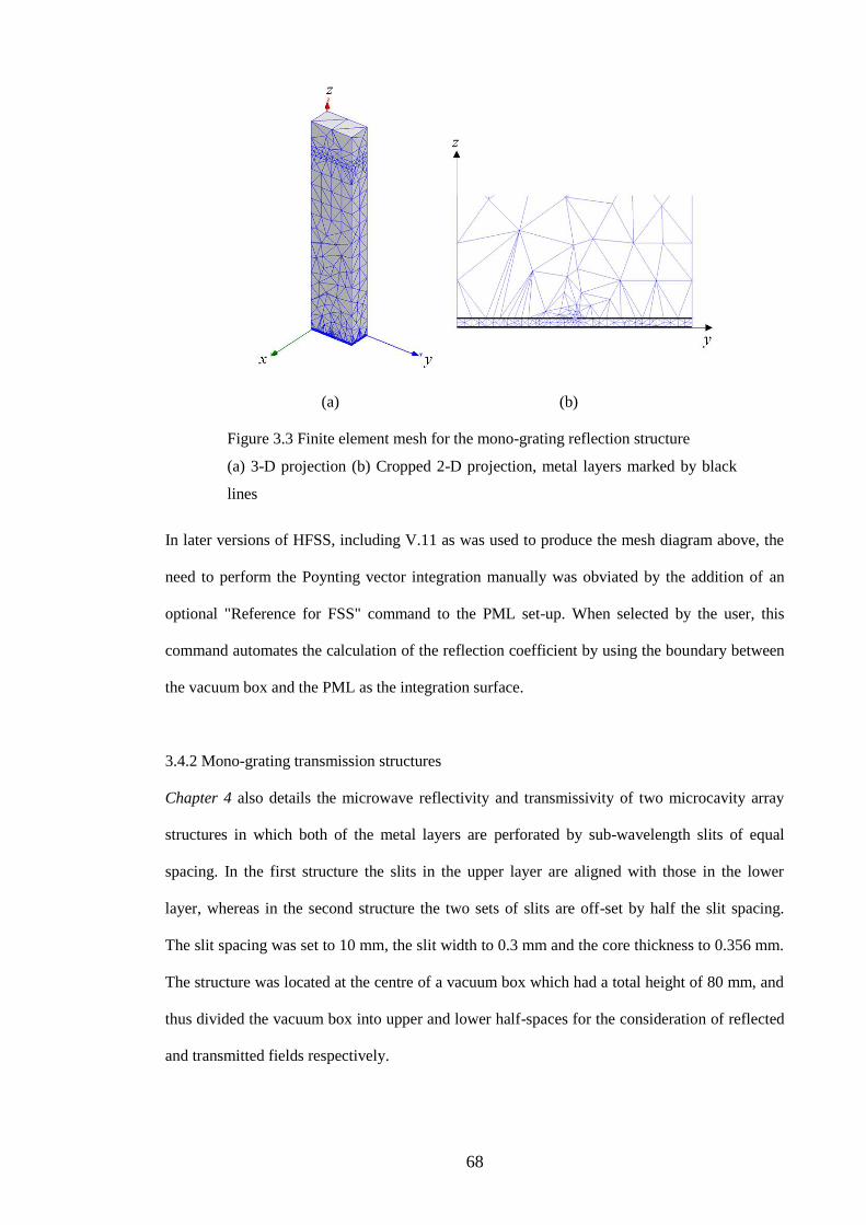
68
(a) (b)
Figure 3.3 Finite element mesh for the mono-grating reflection structure
(a) 3-D projection (b) Cropped 2-D projection, metal layers marked by black
lines
In later versions of HFSS, including V.11 as was used to produce the mesh diagram above, the
need to perform the Poynting vector integration manually was obviated by the addition of an
optional "Reference for FSS" command to the PML set-up. When selected by the user, this
command automates the calculation of the reflection coefficient by using the boundary between
the vacuum box and the PML as the integration surface.
3.4.2 Mono-grating transmission structures
Chapter 4 also details the microwave reflectivity and transmissivity of two microcavity array
structures in which both of the metal layers are perforated by sub-wavelength slits of equal
spacing. In the first structure the slits in the upper layer are aligned with those in the lower
layer, whereas in the second structure the two sets of slits are off-set by half the slit spacing.
The slit spacing was set to 10 mm, the slit width to 0.3 mm and the core thickness to 0.356 mm.
The structure was located at the centre of a vacuum box which had a total height of 80 mm, and
thus divided the vacuum box into upper and lower half-spaces for the consideration of reflected
and transmitted fields respectively.
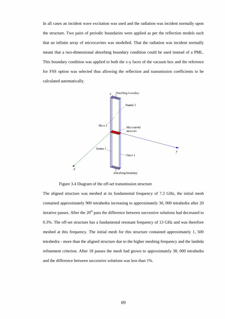
69
In all cases an incident wave excitation was used and the radiation was incident normally upon
the structure. Two pairs of periodic boundaries were applied as per the reflection models such
that an infinite array of microcavites was modelled. That the radiation was incident normally
meant that a two-dimensional absorbing boundary condition could be used instead of a PML.
This boundary condition was applied to both the x-y faces of the vacuum box and the reference
for FSS option was selected thus allowing the reflection and transmission coefficients to be
calculated automatically.
Figure 3.4 Diagram of the off-set transmission structure
The aligned structure was meshed at its fundamental frequency of 7.2 GHz, the initial mesh
contained approximately 900 tetrahedra increasing to approximately 30, 000 tetrahedra after 20
iterative passes. After the 20th pass the difference between successive solutions had decreased to
0.3%. The off-set structure has a fundamental resonant frequency of 13 GHz and was therefore
meshed at this frequency. The initial mesh for this structure contained approximately 1, 500
tetrahedra - more than the aligned structure due to the higher meshing frequency and the lambda
refinement criterion. After 18 passes the mesh had grown to approximately 38, 000 tetrahedra
and the difference between successive solutions was less than 1%.

70
3.4.3 Bi-grating reflection structures
In Chapter 5 two sets of mutually orthogonal sub-wavelength slits are cut into the upper metal
layer thus dividing it into an array of square patches. This bi-grating structure therefore
possesses 90° rotational symmetry and the focus of Chapter 5 is exploring the incident and
azimuthal angle dependence of the modes this structure supports. Extensive modelling of this
structure was undertaken in order to understand the character of these modes.
In all cases the microcavity structure lies parallel to the x-y plane and the inter-slit spacing is 10
mm for both sets of slits, the slits themselves are 0.3 mm wide. The dielectric core material is
0.356 mm thick FR4 with complex permittivity (4.17 + i0.07) and the metal layers are 0.018
mm thick copper with conductivity 5.8.107 S/m. The microcavity structure resides at the bottom
of a 40 mm high vacuum box, to the top of which is added a 7.5 mm thick PML. The structures
were excited with an incident wave over a variety of incident and azimuthal angles, hence the
use of a PML boundary condition.
The model was constructed such that the slit was to the periphery of the unit cell and the square
metal patch in the centre, this is in contrast to the mono-grating structure which has the slit
located at the centre of the unit cell. However, the application of the periodic boundary
conditions merely requires that the material properties of the object which has an interface with
the master boundary are the same as those which has an interface with the slave boundary,
hence there is a choice in where to locate the boundaries.
Several models were solved over a range of incident angles, including 57.4°. Initial results for
this structure were poor with the reflection coefficient values exceeding unity at frequencies
below 6 GHz. These non-physical results were eliminated by seeding the mesh. Three separate
mesh seeding criteria were applied: to the vacuum box a target maximum tetrahedral length of 1
mm was specified within the bounds of the total number of tetrahedra within the vacuum box
not exceeding 1, 000. Within the dielectric core the target maximum tetrahedral length was set
to 0.5 mm, again with the restriction that the total number of tetrahedra did not exceed 1, 000.

71
Finally the surface of intersection between the vacuum box and the PML was set a target
maximum element length of 1 mm but with no restriction on the number of triangles rather than
tetrahedra as this is a surface rather than a volume. For this model the initial mesh contained
approximately 32, 000 - a consequence of the strict mesh seeding and the addition of the second
set of slits. The field gradient is highest within the slits hence the mesh density is also high
therein. The bi-grating model has approximately 20 mm of combined slit length - five times that
of the mono-grating model, hence more tetrahedra are required. After five passes the number of
tetrahedra had reached approximately 55, 000 and the difference between successive solutions
was less than 0.1%.
Shown in Figure 3.5 below, is the model geometry, Figure 3.5(a) and the finite element mesh on
the vacuum box only, Figure 3.5(b). The mesh exhibits a high degree of regularity and the
results of seeding the intersection of the vacuum box and PML are also apparent: there is a very
fine mesh in this area. This fine mesh improves the accuracy of the field solution and therefore
of the reflection coefficient values as this surface is used to perform the automated Poynting
vector integration.

72
(a)
(b)
Figure 3.5 Diagram showing the bi-grating model
(a) the model geometry (b) the finite element mesh
3.4.4 Tri-grating reflection structures
Chapter 6 considers the microwave reflectivity of structures in which there are three sets of sub-
wavelength slits in the upper metal layer, each orientated at 60° to the other two. These
73
structures therefore exhibit 60° rotational symmetry and support a greater number of modes than
either the mono-grating or bi-grating structures.
Two hexagonally symmetric configurations were considered: on the first sample all three sets of
slits intersect at common points creating an array of equilateral triangles of side equal to 32l
where l is the repeat period of each set of slits measured parallel to the grating vector, see Figure
3.6(a). In the second structure each set of grooves is off-set by half its repeat period relative to
the other two sets hence all points of intersection feature slits from only two of the three sets
and a pattern of hexagons interspersed with equilateral triangles both of side 3l is formed, see
Figure 3.6(b).
Inputting these geometries into HFSS is somewhat more complex than either the mono-grating
or bi-grating structures which could be formed from simple primitive drawing commands since
they feature only parallel or perpendicular sides. The 60° rotational symmetry of the tri-grating
structures can be dealt with by using spherical rather than Cartesian co-ordinates or equivalently
by using the rotate command rather than translate command within HFSS. Using Cartesian co-
ordinates introduces a degree of inaccuracy since the projection of the unit cell side onto the
axes involves taking sine of the 60° angle which is an irrational number. This irrational number
must be rounded to a finite number of decimal places before it can be entered into the model but
the accumulation of these input rounding errors can result in a meshing error and the model may
fail to solve.

74
Figure 3.6 The tri-grating sample geometries (not to scale) and the co-ordinate
system used (a) 3-D projection of tri-grating 1 (b) 3-D projection of tri-grating
2, tm = 18 μm, tc = 356 μm, ws = 0.3 mm, 12 gg = 10 mm, is the polar
angle, is the azimuthal angle
Figure 3.7 shows the various stages in the construction of the upper metal layer of the tri-
gratings. Start with a copper layer 0.018 mm thick, set the x- and y-dimensions to 30 mm
arbitrarily. Then create an array of slits 0.3 mm wide, 0.018 mm deep and spaced by 10 mm -
Figure 3.7(a). Create a copy of the slits then rotate these by 60° about the z-axis using the rotate
command - Figure 3.7(b). Repeat this process but rotate by -60° - Figure 3.7(c). Now all three
sets of slits have been created, at the correct spacing and orientation and no irrational numbers
have been input.

75
Figure 3.7 Forming the tri-grating structures without inputting irrational numbers
(a) metal plate (30 x 30) mm with three slits spaced 10 mm apart (b) second set of
slits added and rotated by 60° about the z-axis (c) third set of slits added and
rotated by -60° about the z-axis (d) translation of first set of slits by 5 mm in the z-
direction (e) subtraction of all three sets of slits from the metal layer, two unit
cells can be seen
Subtracting the slits from the copper will form the upper metal layer of tri-grating sample 1 as
shown in Figure 3.7(c). Before performing the subtraction, translate the original set of slits by 5

76
mm in the x-direction, Figure 3.7(d), a subsequent subtraction process yields the upper metal
layer of tri-grating 2, Figure 3.7(e). Note that because the translation was entirely parallel to one
of the Cartesian axes no irrational numbers were input. A similar albeit simpler process can be
followed to form the lower metal layer, dielectric core and vacuum box. The excess cells can be
removed by the use of further rotate, translate, and split about axis or subtract commands, and
will yield accurate results without the need for rounded irrational numbers to be input, provided
that all translations take place parallel to the x- or y-axis and parallel to one of the k-vectors of
the structure.
In a similar manner to the preceding mono-grating and bi-grating structures, periodic boundary
conditions were applied and a 7.5 mm thick PML was added to top of the 40 mm high vacuum
box. The established permittivity and conductivity values for FR4 and copper respectively were
applied. As with the bi-grating, it was found that seeding the mesh helped to improve the
accuracy of the reflectivity values. The same seeding criteria were applied to both tri-gratings as
were applied to the bi-gratings, typically starting meshes contained approximately 40, 000
tetrahedra and converged after 5 - 6 passes whereupon the mesh had grown to around 70, 000
tetrahedra. Plots of selected sections of the final meshes are shown in Figure 3.8: it is clear that
seeding has resulted in a highly dense mesh in both cores and on the integration surfaces.

77
(a) (b)
Figure 3.8 Plots of selected parts of the final finite element mesh for the tri-
grating structures (a) for tri-grating 1 (b) for tri-grating 2
3.4.5 Broadband structures
Chapter 7 details the response of several microcavity array configurations designed to afford
increased absorption bandwidth over the structures hitherto investigated. Four different
strategies were pursued in an attempt to maximise absorption bandwidth whilst minimising the
thickness of a the mono-grating structure. The first strategy involved alternating between two
inter-slit distances such that the modes excited in adjacent cavities would correspond to
different frequencies - two fundamental resonances would result. Another similar strategy with
the same goal was to alternate between two different values of core material permittivity. Both
these strategies used modelling approaches that have been covered in detail in earlier sections
hence no repeat of that treatment is given here.
3.4.5.1 Non-parallel slits
Of the two remaining strategies, the first introduces the concept of non-parallel slits with the
intention being to excite a continuous albeit finite range of resonant frequencies. Every other slit
has a saw-toothed shape, the period of the saw-tooth being 40 mm and its amplitude being 2
mm. Thus the distance between adjacent slits varies from 8 mm to 12 mm and back to 8 mm

78
every 40 mm along the y-axis, see Figure 3.9. Successive saw-tooth slits are half a period out of
phase with each other, thus making the overall period of the structure 40 mm in the x-direction.
Figure 3.9 Multiple continuous repeat periods with alternate saw-tooth slits
The saw-toothed slits were formed in the upper metal layer by using the polyline command in
HFSS, whereby the user inputs the locations of the corners or vertices of a two-dimensional
object. This two-dimensional object is then swept along an axis to form a three-dimensional
structure. In this case the polyline was swept along a vector 0.018 mm along, parallel to the z-
axis (out of the page) to form an object which was then subtracted from the upper metal layer,
thus leaving a saw-toothed aperture. The application of two pairs of periodic boundaries then
results in an infinite array of the unit cell being modelled. This takes account of the periodicity
in both the x- and y-directions. All other aspects of this design were formed by use of the
primitive drawing commands for forming sheets and cuboids. Material properties were as per
the standard mono-grating: dielectric core material was FR4 with relative permittivity (4.17 +
i0.07), all metal layers were copper with conductivity 5.8.107 S/m.
No mesh seeding was undertaken for the models of this structure as good convergence and
reliable, accurate results were obtained without such intervention. Since the unit cell for this
structure measures (40 x 40) mm rather than (4 x 10) mm as for the standard mono-grating, a

79
much larger initial mesh was required: typically 4, 000 tetrahedra were required initially,
increasing to approximately 48, 000 after 18 passes, whereupon the solution converged.
3.4.5.2 Multi-layer structures
The third method for achieving additional absorption bandwidth consisted of stacking a series of
mono-grating transmission structures, each of identical period but differing core material
properties, one upon the other. Three transmission structures were backed by one reflection
structure thus forming a four-layer, stacked microcavity absorber, see Figure 3.10.
Figure 3.10 Multi-layer microcavity structure
(a) 3-D projection of multi-layer structure, 2 periods shown (b) end projection
of multi-layer
The multi-layer structure consists of 4 layers each with a period of 10 mm and slit width of 0.3
mm. The four layers are stacked one upon the other such that their slits are aligned: the top three
layers have slits in both copper layers to allow penetration of the incident wave to the lower
layers. Starting with the lowermost layer and working upwards, the dielectric materials used
were: alumina (Al2O3) FR4, polyester (PET) and air. The complex permittivities of PET and
alumina are εr = (3.2 + 0.0096i) and εr = (9.4 + 0.0564i) respectively and were obtained from
the materials database within HFSS. All metal layers were assigned the conductivity value of
copper.
The period of the structure in the y-direction is 10 mm, the structure is not periodic in the x-
dimension, therefore the x-dimension of the unit was set to 4 mm. Two pairs of periodic
boundaries were applied to represent an infinite array. The structure was excited with a

80
normally incident wave hence an absorbing boundary condition rather than a PML was used.
Whilst no mesh seeding was found to be necessary, the inclusion of four layers resulted in a
starting mesh of approximately 7, 000 tetrahedra. Furthermore the model was slow to converge
and required 18 passes and approximately 102, 000 tetrahedra for the variation between
successive solutions to fall to 1%.
3.5 Summary
This chapter has described the basis of the finite element method and the manner in which
HFSS can be applied to simulate the behaviour of the microcavity arrays. The method of
inputting the geometries of the various microcavity structures has been detailed and the types of
boundary which can be applied have been described and explained. The manner in which HFSS
deals with dielectric materials is covered as is the use of a surface impedance approximation in
simulating the behaviour of metals in a computationally efficient manner. The ability to tailor
the finite element mesh to suit a particular problem geometry has also been presented with
reference to the microcavity bi-grating and tri-grating structures.

81
Chapter 4
The microwave reflectivity and transmissivity of a low-loss dielectric
layer disposed between two metallic layers perforated periodically by
sub-wavelength slits
4.1 Introduction
Conventional materials for the attenuation of centimetric electromagnetic radiation have
historically been limited to a minimum thickness of a quarter-wavelength, with examples of
such materials including Salisbury screens (Salisbury (1952)) and Dallenbach layers (Knott
(1993)), this limitation can present significant practical problems in terms of thickness and
weight penalties incurred. In this chapter ultra-thin cavities are studied for use as low-profile
resonant absorbers: two metal layers are spaced by a dielectric whose thickness is grossly sub-
wavelength, the uppermost of which is perforated periodically by a single set of continuous sub-
wavelength slits. Hibbins et al (2006) have applied this type of geometry to produce absorption
in the optical regime and have shown that the structure supports a series of resonant modes
which can be likened to those supported by a Fabry-Perot etalon (Takakura (2001)). This
structure can readily be scaled to produce absorption at radio frequencies. Furthermore, by
perforating both metal layers, it is possible to selectively transmit radiation through the
structure, the wavelength of which is more than an order of magnitude greater than the structure
thickness.
This first experimental chapter shall focus on the reflectivity and transmissivity of the ultra-thin
cavities as a function of the incident (or polar) angle, and the azimuthal angle of the structure
with respect to the incident wave. The specular reflectivity of and polarisation conversation
produced by the structures is studied experimentally. The nature of the resonant modes
supported by the structures is investigated by using a finite element model. The model is also
used to determine how the absorption depth can be maximised by altering structure geometry
and material properties. The transmission of radiation through structures in which both metal
layers are perforated is also studied and explained by reference to the finite element model. A

82
significant proportion of the work contained within this chapter was published by Hibbins et al
(2004) and reference is hereby directed to that publication.
4.2 Background
That metal layers perforated with sub-wavelength apertures can transmit more radiation than is
incident upon the apertures themselves, has been reported by many including Ebbesen et al
(1998) and Suckling (2007). Both multiple diffraction and the excitation of surface plasmon
polaritons have been demonstrated as being important in mediating this effect (see Hibbins
(2004)). According to classical waveguide theory (Collin (1991)) a slit in a metal surface can
support the propagation of TEM modes that do not exhibit a minimum cut-off frequency, in
contrast to a hole which can support either TE or TM modes only above a certain frequency.
Two closely-spaced metal layers, the uppermost perforated periodically with sub-wavelength
slits of spacing L, constitutes an array of open-ended cavities. These cavities will support a
series of pseudo Fabry-Perot resonances, the approximate frequencies, fN of which can be
obtained from:
nL
NcfN
2 (4.1)
Here, N is the order of the Fabry-Perot mode, c is the speed of light in vacuo and n is the
refractive index of the dielectric material used to separate the two metal layers. This resonance
condition (equation (4.1)) arises from constructive interference between waves within the cavity
being successively reflected from the open ends of the cavity, due to the impedance mis-match
present at these interfaces. This constructive interference results in resonant enhancement of the
electromagnetic fields and the steady-state amplitude of the resonant mode can be more than an
order of magnitude greater than the injected field.
Resonant enhancement plays a key role in the high transmission efficiency of the structures in
which both metal layers are perforated. The sub-wavelength dimensions of the slits means that

83
they intercept only a small proportion of the radio wave energy that is incident on the structure
as a whole. This small proportion of the total incident energy is coupled through the slits in the
upper metal layer into the resonant mode within the cavity. The impedance mis-match at the
slits in the lower metal layer results in most of the energy associated with the mode being
internally reflected back along the cavity and only a small proportion coupling out through the
slit into the surrounding medium (typically air). Hence the initial proportion of energy incident
on the upper slits which is transmitted through the structure and out of the slits in the lower
metal layer is low.
However, the resonant enhancement that occurs within the cavity results in the amplitude of the
mode incident on the slits in the lower metal layer being much larger than that of the incident
wave. High transmission efficiencies can therefore result from a small proportion of a highly-
enhanced field being coupled through the slits in the lower metal layer.
Equation (4.1) predicts the resonant frequencies of the modes supported by the microcavities at
normal incidence and with the electric field of the incident wave perpendicular to the slits, and
an azimuthal angle 0 . However, rotation of the sample away from 0 and or irradiation
at any angle other than normal incidence results in equation (4.1) becoming increasingly
inaccurate. In such cases the resonant frequencies can be predicted by considering the
momentum of the incident photons and resolution of this incident momentum into the x- and y-
directions.
Assume infinitesimal slit width and set λy = 2λg for the fundamental standing wave resonance. It
can then be shown using the equation:
222
0
2
yx kkkn , (4.2)
Where n is the refractive index of the incident medium (n = 1 for vacuum), k0 is the wavevector
of the free-space wave, kx is the wavevector of the wave in the core in the x-direction, and ky is
the wavevector of the wave in the core in y-direction, that:
84
2222
0 sinsin12 gn , (4.3)
Where λ0 is the free-space wavelength.
One important distinction between the responses of the mono-grating to p-polarized and s-
polarization radiation concerns the frequency-stability of the fundamental mode with changing
polar angle. At an azimuthal angle of 0 the frequency given by equation (4.3), is
independent of the polar angle, : hence, the resonance is invariant. At this angle, coupling to
the mode from p-polarized radiation is maximized. There can, however, be no coupling from s-
polarized radiation. By comparison, the s-polarized mode is optimally coupled at an azimuthal
angle of 90 at which angle the frequency given by equation (4.3), is strongly dependent on
the polar angle. The primary consequence of this is a difference in the frequency dependence of
the p- and s-polarized absorption bands at their respective optimally-coupled azimuthal angles.
Any periodic surface will support diffracted orders, the frequency of which can also be
determined by considering the momentum of the incident photons and that supplied by the
grating. The superposition of the incident momentum with that supplied by the grating results
in a quadratic equation in k0:
0cossin2sin12
022
0 gg kkkk . (4.4)
The solution of equation (4.4) yields the limit frequency at which diffraction will occur.
4.3 Experimental
4.3.1 Fabrication of samples
The experimental samples were fabricated from double-sided PCB: a thin, low-loss, dielectric
layer sandwiched between two copper layers. The dimensions and properties of this substrate
material are detailed in Figure 4.1. These dimensions were obtained from the datasheet of the
blank FR4 material and verified to within ±10 μm using a micrometer. It was later found that
these dimensions produced a good fit between modelled and experimental data, although it

85
should be emphasised that within narrow limits (approximately 1% – 2%) there are a number of
combinations of the principal dimensions and material properties which when input to the HFSS
model that produce a good match to the theoretical data. This may be due in part to the
uncertainties in the HFSS solution which are typically quoted as ±2% (Ansys).
Figure 4.1 Cross-section through the substrate material. The dielectric core is
FR4 – a Glass Reinforced Plastic (GRP) composite material with a permittivity
of (4.17 + i0.07)
Parallel slits 0.3 mm wide spaced every 10 mm were formed in the copper layers by using a
chemical etchant to selectively remove the copper. This approach was used to fabricate one
sample which had slits in only the uppermost copper layer, and hence did not transmit any
radiation but served only as an absorber, and two samples which had slits in both copper layers.
These latter samples are capable of transmitting and absorbing radiation. In the first of these two
transmission samples, the slits in the upper and lower copper layers are aligned with each other,
the second transmission sample the slits are off-set by 5 mm – half the repeat period of the
structure. These two configurations represent the two extreme cases: perfect alignment and
perfect misalignment, see Figure 4.2.
With reference to Figure 4.2, ws is the slit width and is equal to 0.3 mm in all cases, λg is the
repeat period of the structure and is everywhere equal to 10 mm. The thickness of the metal
layers, tm, is 18 μm, and the thickness of the core tc is fixed at 356 μm.

86
(a)
(b)
(c)
Figure 4.2 Cross-section through the microcavity samples (a) the reflection
sample (b) the first transmission sample with slits perfectly aligned (c) the
second transmission sample with slits perfectly mis-aligned
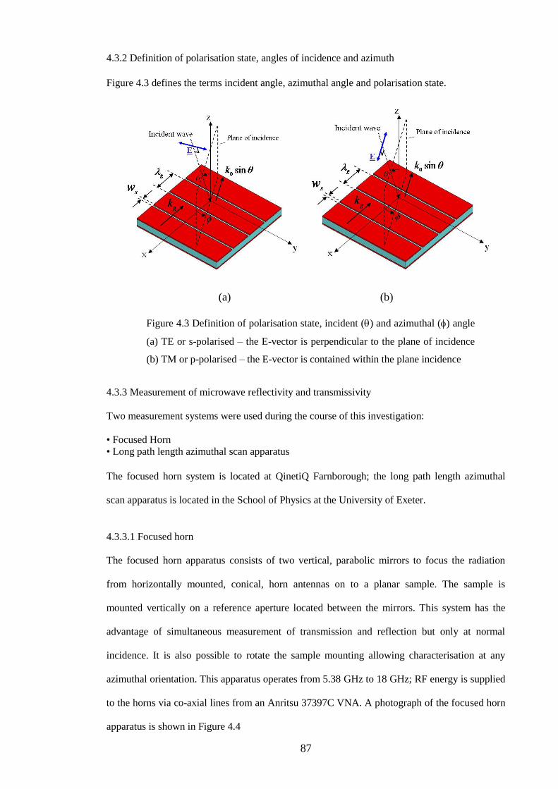
87
4.3.2 Definition of polarisation state, angles of incidence and azimuth
Figure 4.3 defines the terms incident angle, azimuthal angle and polarisation state.
(a) (b)
Figure 4.3 Definition of polarisation state, incident () and azimuthal () angle
(a) TE or s-polarised – the E-vector is perpendicular to the plane of incidence
(b) TM or p-polarised – the E-vector is contained within the plane incidence
4.3.3 Measurement of microwave reflectivity and transmissivity
Two measurement systems were used during the course of this investigation:
• Focused Horn
• Long path length azimuthal scan apparatus
The focused horn system is located at QinetiQ Farnborough; the long path length azimuthal
scan apparatus is located in the School of Physics at the University of Exeter.
4.3.3.1 Focused horn
The focused horn apparatus consists of two vertical, parabolic mirrors to focus the radiation
from horizontally mounted, conical, horn antennas on to a planar sample. The sample is
mounted vertically on a reference aperture located between the mirrors. This system has the
advantage of simultaneous measurement of transmission and reflection but only at normal
incidence. It is also possible to rotate the sample mounting allowing characterisation at any
azimuthal orientation. This apparatus operates from 5.38 GHz to 18 GHz; RF energy is supplied
to the horns via co-axial lines from an Anritsu 37397C VNA. A photograph of the focused horn
apparatus is shown in Figure 4.4

88
Figure 4.4 Photograph of the focused horn apparatus The VNA can be seen in
the background, the reference aperture can be seen in the centre. The focal
length of the system is adjusted by a stepper motor attached to the nearest
mirror (out of shot to the left)
It is possible to calculate the complex permittivity and permeability of a dielectric sample using
the reflection and transmission data from the focused horn. This is routinely done at QinetiQ
Farnborough using the theory due to Nicholson and Ross (1970) and Weir (1974) written in the
form of a MathCAD program. This technique was applied to calculate the permittivity and
permeability of the FR4 core material of the VTRAM. These data are prerequisites for
modelling the VTRAM using the finite element model.
4.3.3.2 Long path length azimuthal scan apparatus
Bi-static reflectivity measurements were carried out using the long path length apparatus at the
University of Exeter. An HP8757D scalar network analyser is connected to Narda microwave
horns via co-axial cables. Spherical mirrors focus the microwave radiation onto the sample and
ensure that the degree of wavefront curvature is minimal. The sample is mounted on a non-
conducting pedestal. This pedestal is rotated in azimuth in 0.5-degree steps by a stepper motor
controlled via a PC. This set-up therefore has the advantage of fine control of azimuthal
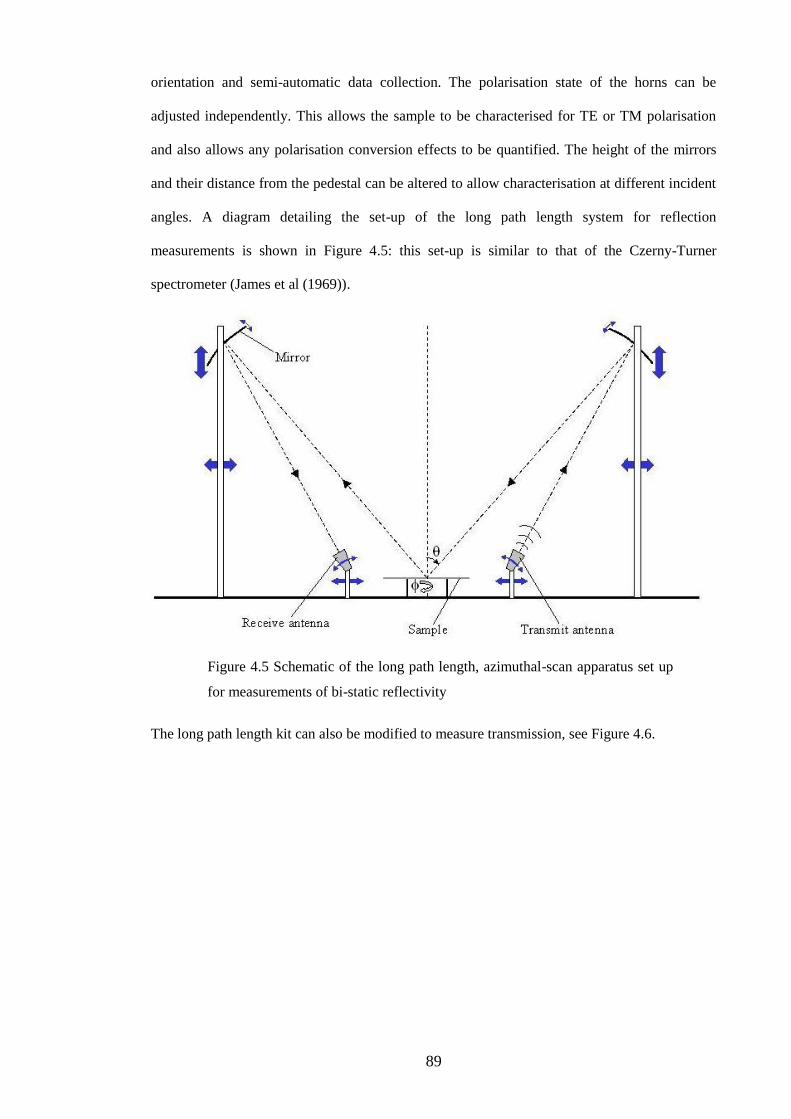
89
orientation and semi-automatic data collection. The polarisation state of the horns can be
adjusted independently. This allows the sample to be characterised for TE or TM polarisation
and also allows any polarisation conversion effects to be quantified. The height of the mirrors
and their distance from the pedestal can be altered to allow characterisation at different incident
angles. A diagram detailing the set-up of the long path length system for reflection
measurements is shown in Figure 4.5: this set-up is similar to that of the Czerny-Turner
spectrometer (James et al (1969)).
Figure 4.5 Schematic of the long path length, azimuthal-scan apparatus set up
for measurements of bi-static reflectivity
The long path length kit can also be modified to measure transmission, see Figure 4.6.
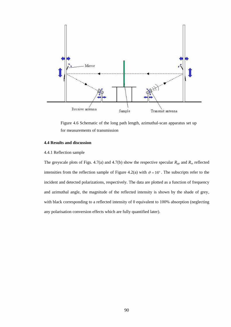
90
Figure 4.6 Schematic of the long path length, azimuthal-scan apparatus set up
for measurements of transmission
4.4 Results and discussion
4.4.1 Reflection sample
The greyscale plots of Figs. 4.7(a) and 4.7(b) show the respective specular Rpp and Rss reflected
intensities from the reflection sample of Figure 4.2(a) with 16 . The subscripts refer to the
incident and detected polarizations, respectively. The data are plotted as a function of frequency
and azimuthal angle, the magnitude of the reflected intensity is shown by the shade of grey,
with black corresponding to a reflected intensity of 0 equivalent to 100% absorption (neglecting
any polarisation conversion effects which are fully quantified later).

91
Figure 4.7 Experimental Reflected intensities for reflection sample shown as
greyscale plots (a) Rpp data as a function of frequency and azimuthal angle at
º16 (b) Rss data as a function of frequency and azimuthal angle at º16
(c) Rpp data as a function of frequency and azimuthal angle at º57 , dashed
line corresponds to expected position of diffraction edge (d) Rss data as a
function of frequency and azimuthal angle at º57 .
The dark bands at 7 GHz and 14.6 GHz in Figure 4.7(a) indicate strong absorption. Using (4.1),
with (εr = 4.17 +0.07i) for the relative permittivity of the dielectric core one can identify the
mode at ≈ 7 GHz as the fundamental resonance. Similarly, the mode at ≈ 14.6 GHz is the
second order mode. The fundamental resonance is strongest at = 0° where the component of
the incident electric field vector perpendicular to the slits is greatest. It becomes progressively
shallower as the grating is rotated; with no resonance occurring at = 90° since there is no
component of the electric field across the slit. Conversely, the fundamental absorption band in
Figure 4.7(b), for s-polarized radiation shows greatest absorption at = 90°and no absorption
at 0. Again this is due to the electric field lying parallel to the slits for 0 with s-
polarization. Figures 4.7(c) and 4.7(d) are Rpp and Rss respectively for the mono-grating at =
92
57°. Now the bands demonstrate a much higher degree of curvature in order to satisfy
conservation of momentum (equation (4.3)). With reference to Fig. 4(c), the faint, highly
curved band centred on = 0° is due to conical diffraction. The solution of equation (4.4) has
been plotted as a dashed line on Figure 4.7(c) and closely follows the diffraction feature as
expected.
As noted above, at an azimuthal angle of 0 the frequency given by equation. (4.3), is
independent of the polar angle: hence, the resonance is invariant. At this angle, coupling to the
mode from p-polarized radiation is maximized. There can, however, be no coupling from s-
polarized radiation. By comparison, the s-polarized mode is optimally coupled at an azimuthal
angle of 90 at which angle the frequency given by equation (4.3), is strongly dependent on the
polar angle. The primary consequence of this is a difference in the frequency dependence of the
p- and s-polarized absorption bands at their respective optimally-coupled azimuthal angles and
this is indeed evident from the greyscale plots of Figure 4.7 and the line plots of Figure 4.8.
The finite element model was used to simulate the reflectivity of the reflection sample between
5 GHz and 18 GHz, at an incident angle of 4.57 and an azimuthal angle of 0 , for p-
polarised radiation. A comparison between this simulated reflectivity and that measured at the
same angles is shown in Figure 4.9. There is very good agreement between the measured and
modelled data with the fundamental and second order modes appearing as resonances at 7.1
GHz and 13.9 GHz respectively. The diffraction edge is also visible at 16.5 GHz although it is
more pronounced with the experimental data than the theory. This may be a finite size effect: if
the diffracted beam misses the mirrors and therefore the receiving horn antenna in the
experimental set-up then it makes no contribution to the overall received signal. In the model
however, the received signal is calculated by integrating the time-averaged Poynting vector over
the appropriate plane, hence even though the diffracted beam is oblique to the integration plane
there is still some contribution to the integral thus increasing the overall received signal.

93
(a)
(b)
Figure 4.8 Line plots of the reflectivity of the reflection sample as measured
experimentally at incident angles of 16 and 4.57 for (a) p-
polarisation and 0 (b) s-polarisation and 90

94
Figure 4.9 Reflectivity of the reflection sample as measured experimentally
and simulated by the finite element model: P-polarisation incident at 4.57
and 0
The finite element model can also be used to investigate the nature of the resonant modes. In
Figure 4.10(a) the instantaneous magnitude of the electric field within the dielectric core has
been plotted at a phase corresponding to peak field strength and a frequency of 7.1 GHz – that
of the fundamental mode. In this case the slit is shown at the centre of one period or unit cell of
the structure with half a cavity to each side of the slit. The colour represents the strength of the
field with red equating to a field strength of 20 V/m (20 times the incident field) and blue to 0
V/m. The field decreases from a maximum of over 20 V/m in the vicinity of the slit, to zero
mid-way between slits or in this case at the edges of the unit cell: it is apparent that between
adjacent slits, the mode completes half a cycle.
Also evident from Figure 4.10(a), is a region of zero field strength on the inner surface of the
lower metal layer immediately below the slit. The origin of this zero field region and the
detailed behaviour of the electric field within the slit can be elucidated by using the finite
element to plot the value of the z-component of the field along a line through the centre of the

95
FR4 core parallel to the y-axis see Figure 4.10(b) – and to plot the electric field vector within
the dielectric core in the vicinity of the slit – see Figure 4.10(c).
(a)
(b)
(c)
Figure 4.10 The electric field within the dielectric core of the microcavities as
simulated by HFSS: scale runs from 0 V/m (blue), to 20 V/m (red) incident
wave amplitude 1 V/m (a) Instantaneous magnitude of the electric field at 7.1
GHz, at a phase corresponding to peak field strength, the black lines represent
the copper layers (b) z-component of the electric field along a line through the
centre of the core parallel to the x-axis (c) Instantaneous the electric field
vector at 7.1 GHz, at a phase corresponding to peak field strength

96
As described by Hibbins et al (2004) the incident wave creates regions of enhanced charge
density on either side of the slit, a consequence of which is that the mode within the core must
complete another half-cycle within the width of the slit. This phase reversal within the slit
results in the field in the centre of the slit being parallel to the plane of the sample or in this case
parallel to the x-axis – see Figure 4.10(c). As the tangential component of the electric field
across an interface must be continuous, and the field inside a perfect conductor (metals
approximate perfect conductors at microwave frequencies) is zero, a region of zero field
strength is exhibited on the lower metal layer below the centre of the slit.
In this structure the slit width ws = 0.3 mm, hence the mode has suffered ―phase compression;‖
(Hibbins et al (2004)) being forced to undergo a π-radians phase change in only 0.3 mm,
whereas in the space between the slits the same phase change occurred over 9.7 mm, this is
demonstrated graphically in Figure 4.10(b). Hence within one complete period of the structure
the mode has undergone one complete cycle of 2π radians: π radians between adjacent slits as
would be expected, and an additional π radians within the slit. The period of the mode and that
of the structure are equal for the fundamental, this structure would therefore be expected to
support any modes for which N in equation 4.1 is odd but not those for which N is even.
The second-order mode for s-polarized radiation, shown as the dark bands between 14 GHz and
17 GHz in Figs. 4.7(b) and 4.7(d), cannot be coupled to at = 90° (unlike the fundamental
mode). Again this can be understood by considering the behaviour of the standing wave fields
within the core. The second order mode undergoes a phase change of 2π-radians between the
slits: when added to the enforced π-radians phase change across the slit, this results in a total
phase change of 3π-radians within one period of the structure. Therefore, at any given slit the
field resulting from the wave coupled in through that slit will be π-radians out of phase with the
field coupled in through the adjacent slits. This results in destructive interference and prevents
propagation of the mode. To permit propagation of the second order mode some additional
phase off-set is needed. At normal incidence the fields are in-phase at all slits regardless of the
orientation of the electric vector, and hence the second order mode can never be excited. Off-

97
normal there is a phase difference between slits for p-polarized radiation at all azimuths but for
s-polarization there is no phase difference between slits at = 90°, regardless of the polar
angle, and hence no mode is excited at these orientations. Furthermore, there exists an optimum
incident angle which results in the second order mode having just the right amplitude to balance
the radiative and dissipative losses, and hence maximise the depth of the second-order
resonance.
4.4.2 Optimisation of resonance depth
Consider a wave incident on the surface of the ultra thin cavity structure. A proportion of the
wave incident is reflected in the specular direction from the top metal surface and the remainder
is coupled through the slits into the core. One might expect that the proportion of the incident
energy that is initially coupled through the slits into the core is very small since the slits
themselves constitute a very small proportion of the period. The wave coupled into the core
travels along it until it reaches the next slit whereupon the impedance mismatch at this interface
results it being internally reflected back along the cavity. Interference between waves
successively reflected from the ends of the cavity will result in resonant enhancement when the
inter-slit distance is an integer number of half-wavelengths.
Figure 4.11 Waves incident on the ultra thin cavity structure

98
If say, 3% of the power incident on the cavity structure is coupled through the slits and into the
core then by reciprocity c.3% of the power that got into the core is coupled back out of the slits
or equivalently the total power re-emitted from the core each time would be 3% of 3% or 0.09%
of the total incident power. If this re-emitted wave were in anti-phase with the wave reflected
from the top surface then there would be a degree of destructive interference. However, as the
amplitudes of the specular reflection and the re-emitted wave are 97% and 0.09% respectively,
the net amplitude would be high.
Returning to the waves propagating inside the dielectric core, every cycle c.3% of the power in
the core is re-emitted back out of the slits (0.09% of the total incident energy). Every cycle also
sees another 3% of the incident power coupling into the core. For wavelengths in the core that
are exactly twice the inter-slit distance then modes running back and forth through the cavity
will set-up standing waves - this is the Fabry-Perot etalon resonance condition. At other
wavelengths the waves running back and forth do not interfere constructively and the standing
waves are not set-up.
Regardless of the proportion of the incident energy which initially couples through the slits into
the core, the amplitude of the mode in the core increases progressively over time. The standing
waves are ―fed‖ every cycle by the power coupled through the slits and into the core hence the
amplitude of the waves in the core progressively increases. The greater amplitude of the waves
in the core results in the amplitude of the waves re-emitted through the slits also being greater.
There comes a point after several cycles where the amplitude of waves in the core has been
sufficiently enhanced that the re-emitted wave has an amplitude that is of the same order of
magnitude as the specular reflected wave: in which case there is the potential for totally
destructive interference and hence the overall reflectivity of the material to be very low. When
the radiative loss from the system (the power coupled back out through the slit) exactly matches
the dissipative loss from the system (conversion of energy from the propagating mode to heat
via Joule heating of the dielectric core and metal layers) the net reflectivity of the material will
be zero.

99
Extending this argument still further it can be seen that as the amplitude of the waves in the core
continues to grow the amplitude of the re-emitted waves will eventually become greater than
that of the waves reflected at the top surface (this is known as ―Over-coupling‖). In this case the
two waves cannot interfere in a manner which is completely destructive. The net reflectivity of
the material then starts to rise again.
Consider for a moment that the mechanism for resonant field enhancement and hence
reflectivity reduction as described above, requires a series of cycles in order for the requisite
amplitude to build up. This then raises the question of whether the microcavity arrays and
resonant absorbers in general be circumvented by employing very short pulse times? Another
approach for mitigating absorption and trying to maximise the probability of detection, would
be to use a radar system with a very wide bandwidth – wider than that of the absorber – so that
at some frequencies outside the band of absorption the material’s reflectivity would be high.
These two approaches are in fact equivalent since applying Fourier analysis it can be seen that a
short time pulse is equivalent to a wideband frequency pulse.
The amplitude of the waves in the core cannot continue to rise indefinitely. As the amplitude
increases so does the power loss density PD, (power absorbed per unit volume by the core):
every time the wave propagates back and forth between the slits some power is absorbed by the
dielectric core and by the walls of the cavity. The amount of power absorbed increases as the
square of the amplitude of the wave increases (see (4.5) and (4.6)) and eventually a point is
reached where the power supplied to the wave every cycle (by the proportion of the incident
wave coupling through the slits) is equal to the power absorbed by the wave in the core
propagating between the slits – the net power change is zero and the system has reached a
steady state.

100
With reference to the theoretical model (Ansoft), the power loss density, PD in W/m3 is given by
(4.5):
*.*.Re21 HEikJEPD (4.5)
Where:
E is the electric field strength in V/m
H* is the complex conjugate of the magnetic field strength in A/m
J * is the complex conjugate of the current density in A/m2
Furthermore:
H
EZ (4.6)
Where:
Z is the intrinsic impedance of the medium through which the wave is propagating
E is the electric field in V/m
H is the magnetic field in A/m
From (4.5) and (4.6) it can be seen that the power loss density PD, is proportional to the square
of the electric field.
If, when the system has reached a steady state the amplitude of the re-emitted wave is equal to
that of the specular reflected wave then perfect cancellation occurs and reflection coefficient =
0. In most cases however there is a mismatch but this mismatch can be reduced or removed by
optimising the geometry.
Consider: if in a steady state the amplitude of the wave re-emitted from the slits is less than that
of the specular reflected wave, then to maximise the resonance depth the amplitude of the re-
emitted wave needs increasing. This can be done by increasing the steady state amplitude of the
mode in the core, which in turn is accomplished by reducing the amount of absorption by the
core and metal layers. It might also be expected that increasing the width of the slits to let more
proportionately power into and out of the cavity in (and also reduce the amplitude of the
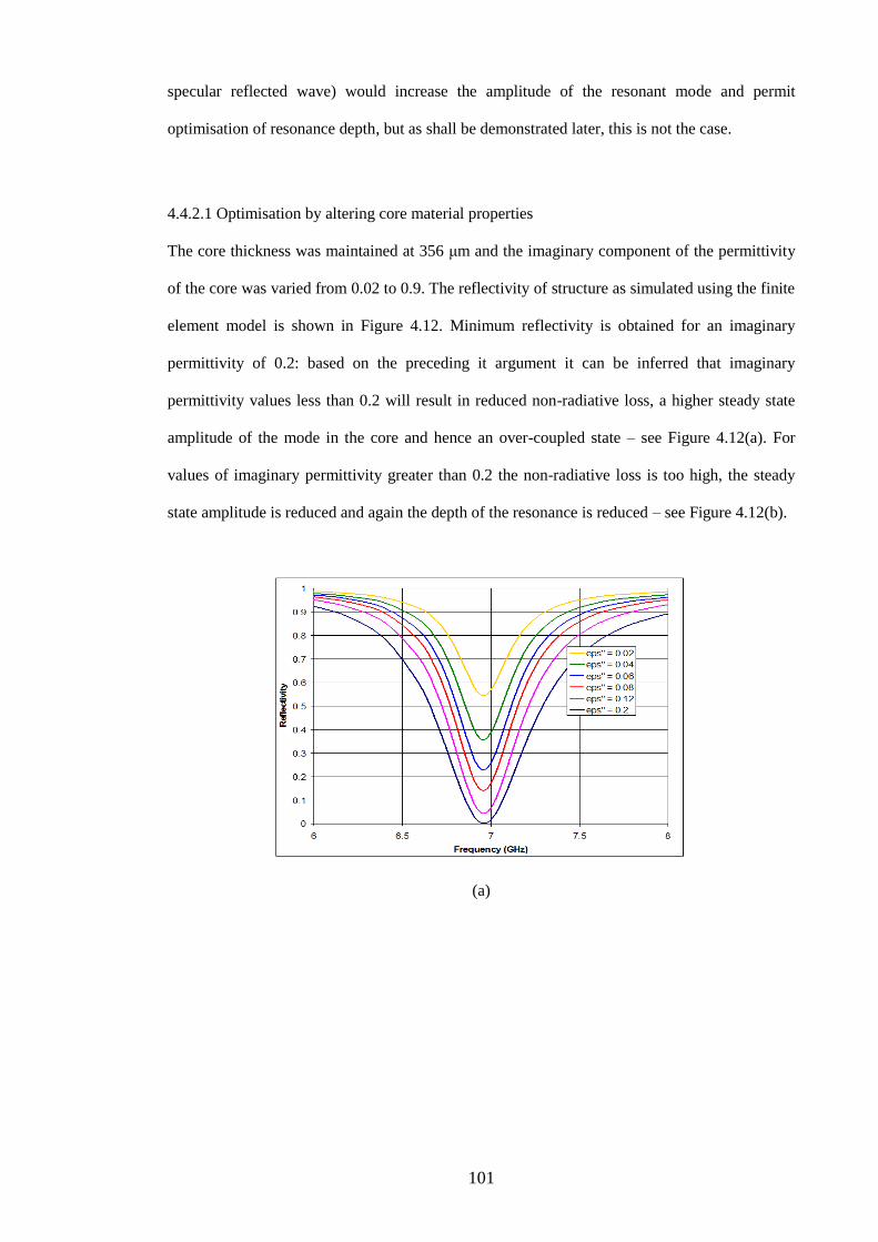
101
specular reflected wave) would increase the amplitude of the resonant mode and permit
optimisation of resonance depth, but as shall be demonstrated later, this is not the case.
4.4.2.1 Optimisation by altering core material properties
The core thickness was maintained at 356 μm and the imaginary component of the permittivity
of the core was varied from 0.02 to 0.9. The reflectivity of structure as simulated using the finite
element model is shown in Figure 4.12. Minimum reflectivity is obtained for an imaginary
permittivity of 0.2: based on the preceding it argument it can be inferred that imaginary
permittivity values less than 0.2 will result in reduced non-radiative loss, a higher steady state
amplitude of the mode in the core and hence an over-coupled state – see Figure 4.12(a). For
values of imaginary permittivity greater than 0.2 the non-radiative loss is too high, the steady
state amplitude is reduced and again the depth of the resonance is reduced – see Figure 4.12(b).
(a)
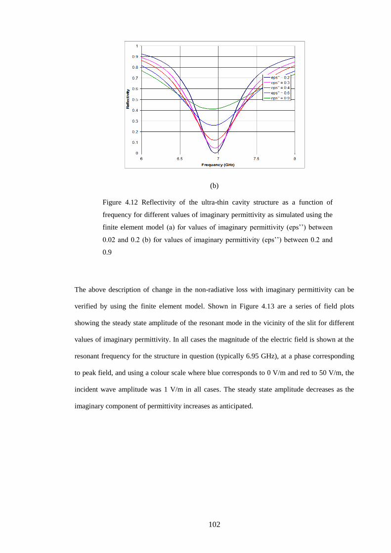
102
(b)
Figure 4.12 Reflectivity of the ultra-thin cavity structure as a function of
frequency for different values of imaginary permittivity as simulated using the
finite element model (a) for values of imaginary permittivity (eps’’) between
0.02 and 0.2 (b) for values of imaginary permittivity (eps’’) between 0.2 and
0.9
The above description of change in the non-radiative loss with imaginary permittivity can be
verified by using the finite element model. Shown in Figure 4.13 are a series of field plots
showing the steady state amplitude of the resonant mode in the vicinity of the slit for different
values of imaginary permittivity. In all cases the magnitude of the electric field is shown at the
resonant frequency for the structure in question (typically 6.95 GHz), at a phase corresponding
to peak field, and using a colour scale where blue corresponds to 0 V/m and red to 50 V/m, the
incident wave amplitude was 1 V/m in all cases. The steady state amplitude decreases as the
imaginary component of permittivity increases as anticipated.

103
Figure 4.13 Field plots showing the instantaneous magnitude of the electric
field for different values of imaginary permittivity, scale runs from 0 V/m
(blue) to 50 V/m (red), incident wave amplitude was 1 V/m in all cases (a)
imaginary permittivity = 0.02 (b) imaginary permittivity = 0.08 (c)imaginary
permittivity = 0.2 (d) imaginary permittivity = 0.4 (e) imaginary permittivity =
0.9
4.4.2.2 Optimisation by altering core thickness
The finite element model was used to simulate the reflectivity of the structure for core
thicknesses between 356 μm and 100 μm, core permittivity was maintained at 4.17 + 0.07i,
results are shown in Figure 4.14.
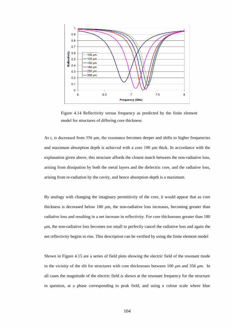
104
Figure 4.14 Reflectivity versus frequency as predicted by the finite element
model for structures of differing core thickness
As tc is decreased from 356 μm, the resonance becomes deeper and shifts to higher frequencies
and maximum absorption depth is achieved with a core 180 μm thick. In accordance with the
explanation given above, this structure affords the closest match between the non-radiative loss,
arising from dissipation by both the metal layers and the dielectric core, and the radiative loss,
arising from re-radiation by the cavity, and hence absorption depth is a maximum.
By analogy with changing the imaginary permittivity of the core, it would appear that as core
thickness is decreased below 180 μm, the non-radiative loss increases, becoming greater than
radiative loss and resulting in a net increase in reflectivity. For core thicknesses greater than 180
μm, the non-radiative loss becomes too small to perfectly cancel the radiative loss and again the
net reflectivity begins to rise. This description can be verified by using the finite element model
Shown in Figure 4.15 are a series of field plots showing the electric field of the resonant mode
in the vicinity of the slit for structures with core thicknesses between 100 μm and 356 μm. In
all cases the magnitude of the electric field is shown at the resonant frequency for the structure
in question, at a phase corresponding to peak field, and using a colour scale where blue

105
corresponds to 0 V/m and red to 40 V/m, again the incident wave amplitude was 1 V/m in all
cases.
The steady state amplitude increases as the core thickness decreases, indicating an increase in
the value of (4.5), the loss density in W/m3. However, the total non-radiative loss in Watts is
calculated by the integral of (4.5) over the volume of the structure, a volume which decreases in
direct proportion to core thickness. Hence as the core thickness decreases there are two
competing factors in determining the change in the non-radiative loss: the increasing amplitude
and the decreasing absorbing volume. However, using (4.6) it is apparent that the loss density is
proportional to the square of the electric field, therefore the value of (4.5) is increasing more
quickly than the volume is decreasing and the net effect of reducing core thickness is to increase
the non-radiative loss.

106
Figure 4.15 Field plots showing the instantaneous magnitude of the electric
field for different core thicknesses, scale runs from 0 V/m (blue) to 40 V/m
(red) and the incident wave amplitude was 1V/m in all cases (a) core thickness
= 100 μm (b) core thickness = 120 μm (c) core thickness = 150 μm (d) core
thickness = 180 μm (e) core thickness = 250 μm (f) core thickness = 356 μm
4.4.2.3 Optimisation by altering slit width
The finite element model was used to explore the effect of changing slit width from 0.025 mm
to 5 mm; results are shown in Figure 4.16. Core permittivity and thickness were fixed at 4.17
+0.07i and 356 μm respectively. The length of the metal patch between slits was kept constant
at a value of 9.7 mm.

107
Figure 4.16 Reflectivity as a function of frequency for the ultra thin cavity
arrays with different slit widths
For slits widths between 0.025 mm and 0.35 mm there is no apparent change in resonance
depth. As slit width increases from 0.35 mm to 5 mm the resonance does begin to deepen but
the rate of change is very small. As slit width is initially increased from 0.025 mm there is a
rapid shift up in frequency, the rate of change in resonant frequency decreases however, and
above 1 mm the frequency barely changes at all.
That there is little change in resonance depth indicates there is no change in the steady state
amplitude of the mode and that width of the slit is not a key factor in determining the proportion
of power from the incident wave which couples into the core. It is an oversimplification to
suggest that only the radiation incident directly on the slit itself couples through it into the core.
As the work of many including Ebbessen (1998) and Suckling (2007) has shown, the slit is
transmitting more power than is directly incident upon it. This can be attributed to the excitation
of surface currents on the metal patches and consequent channelling of power through the slit.
The decrease in resonant frequency with slit width is analogous to work by Suckling et al
(2004) who showed that the transmission frequency of a series of half-wavelength cavities
decreases rapidly as cavity thickness is reduced below a certain value. This shift is a

108
consequence of coupling between surface currents on the metal patches on opposite slides of the
slits. The strength of coupling decreases with increasing slit width and becomes almost
negligible for widths greater than 1 mm; hence there is no further frequency shift for widths
greater than this.
As the slit width is increased the proportion of the dielectric core which is beneath the metal
patches decreases. If the cavities are beginning to act as independent resonators, then any
dissipation will be confined to the region within the cavities – under the metal patches. As the
slit width is increased the proportion of the volume which effectively absorbs is hence reduced
which can affect the structure’s overall reflectivity. Furthermore, the specular reflection will
consist of two components: one from the top surface of the metal patches and one from the
lower metal plane. The latter component will be come more significant as the slit width
increases. The increase in the latter component can alter the relative phases of the reflected and
re-emitted signals which therefore alters the net reflectivity of the structure.
4.4.3 Polarisation conversion effects
It is only the component of the incident electric field that is perpendicular to the slits which can
couple through them and excite the resonant mode in the core. By reciprocity any re-radiation
from the cavity, howsoever excited, will have its electric field aligned perpendicular to the slits.
For p-polarisation maximum coupling occurs for 0 and decreases as cos . If the structure
is irradiated with p-polarisation for 0° < < 90° then coupling to the mode will be sub-
optimum but the mode will still be excited. Furthermore, for this azimuthal range, any re-
radiation by the cavity will have components both parallel and perpendicular to the plane of
incidence: the re-radiated signal contains a mixture of both p- and s-polarized components.
Therefore, whilst the minima observed in the reflectivity spectrum of the reflection sample
typically result from Joule heating of the metal and dielectric layers of the sample, it is also
possible for polarisation conversion by the sample to produce significant reductions in
reflectivity (see: Bryan-Brown (1990) Hallam (2004)).

109
In their standard configuration, a polarisation-converted signal is undetectable by the linearly
polarised antennas of both the focused horn and long path length azimuthal scan systems.
However, additional measurements were performed using the latter, in which the transmitting
and receiving antennas were cross-polarized, hence any polarisation conversion effects could be
detected and quantified. Two configurations were investigated: that in which the transmitting
antenna was p-polarised and the receiver s-polarised so as to measure the p- to s- conversion
coefficient Rps, and similarly the opposite configuration so as to measure Rsp. Results are
presented in form of greyscale contour plots in Figure 4.17 for 16 and 4.57 .
For the lower incident angle, polarization conversion is occurring but only for the more
strongly-coupled fundamental. Peak conversion efficiency is around 50% and occurs at
45 for both Rps and Rsp. For Rps, as increases from 0° towards 90°, the component of the
re-radiated field which is converted is increasing, but this is off-set by a reduction in coupling to
the mode from the incident field, hence conversion peaks at 45° and then decreases again. For
Rsp coupling to the mode increases upon rotation from 0° to 90° azimuth, but the component of
the re-radiated field that is converted decreases so as to off-set this, and again the peak
conversion occurs for 45°.

110
Figure 4.17 Experimental polarisation-converted reflected intensities for
reflection sample shown as greyscale plots (a) Rps data as a function of
frequency and azimuthal angle at º16 (b) Rsp data as a function of
frequency and azimuthal angle at º16 (c) Rps data as a function of
frequency and azimuthal angle at º57 (d) Rsp data as a function of
frequency and azimuthal angle at º57
At the higher incident angle both modes exhibit polarisation conversion: for the fundamental
mode peak conversion efficiency is around 30% whilst for the second order mode it does not
exceed 20%. At the higher angle, the polarisation conversion features appear asymmetric with
peak conversion occurring at less than 45° azimuth for the fundamental and above 45° azimuth
for the second order mode. This may be a consequence of anisotropy in the FR4 core material.
4.4.4 Transmission samples
4.4.4.1 Aligned slits
The transmission through the aligned transmission structure of Figure 4.2(b) was studied by
using the focused horn system. The fractional transmission or transmissivity as a function of

111
frequency is shown in Figure 4.18 for both the focused horn measurement and the
corresponding finite element simulation.
Figure 4.18 Transmission as a function of frequency for the aligned slit
structure as measured using the focused horn system and simulated using the
finite element model
Both experiment and theory demonstrate that the structure transmits approximately one-third of
the radiation incident upon it at its resonant frequency of 7.2 GHz. Using the finite element
model, the instantaneous electric field has been plotted in order to determine the nature of the
resonant mode, see Figure 4.19: in both plots the colour indicates the strength of the field with
blue corresponding to 0 V/m and red to 20 V/m, the incident field amplitude was 1 V/m.
The structure supports an N = 1 resonant mode at 7.2 GHz which undergoes a phase change of π
radians between slits and another π radians within the slit, as would be expected based on the
behaviour of the reflection sample. Note that as documented by Hibbins et al (2004), the field in
the upper slit is π radians out of phase with that at the lower slit and that the net field midway
between the slits at the mid-height of the dielectric core is zero. By further analogy with the
reflection sample, at normal incidence the structure will only support modes for which N in
(4.1) is odd since the sum of the phase change between slits (Nπ) and that within the slit (π)
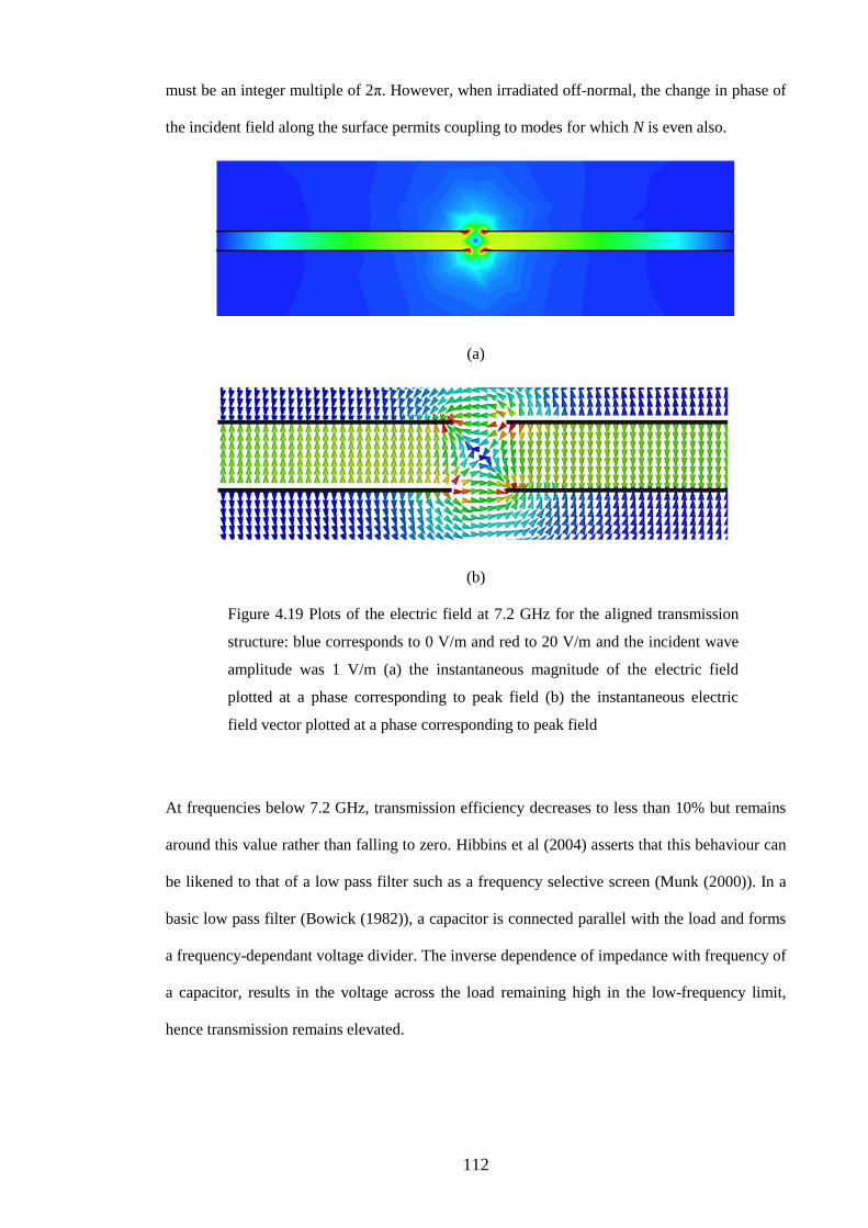
112
must be an integer multiple of 2π. However, when irradiated off-normal, the change in phase of
the incident field along the surface permits coupling to modes for which N is even also.
(a)
(b)
Figure 4.19 Plots of the electric field at 7.2 GHz for the aligned transmission
structure: blue corresponds to 0 V/m and red to 20 V/m and the incident wave
amplitude was 1 V/m (a) the instantaneous magnitude of the electric field
plotted at a phase corresponding to peak field (b) the instantaneous electric
field vector plotted at a phase corresponding to peak field
At frequencies below 7.2 GHz, transmission efficiency decreases to less than 10% but remains
around this value rather than falling to zero. Hibbins et al (2004) asserts that this behaviour can
be likened to that of a low pass filter such as a frequency selective screen (Munk (2000)). In a
basic low pass filter (Bowick (1982)), a capacitor is connected parallel with the load and forms
a frequency-dependant voltage divider. The inverse dependence of impedance with frequency of
a capacitor, results in the voltage across the load remaining high in the low-frequency limit,
hence transmission remains elevated.

113
At 7.6 GHz there is a pronounced minimum in the transmission efficiency. This results from the
aforementioned region of zero field that occurs in the slits at the mid-height of the core, moving
towards the lower aperture at frequencies just above the resonant frequency of 7.2 GHz - an
observation first made by Hibbins et al (2004). When the zero field region is located within the
aperture as occurs at 7.6 GHz, the transmission efficiency is zero. The progressive movement of
the zero field region from the mid-height of the core to the lower aperture has been plotted using
the finite element model – see Figure 4.20: in all cases the fields have been plotted at a phase
corresponding to peak field and using a scale where blue corresponds to 0 V/m and red to 20
V/m, the incident field amplitude was 1 V/m.
(a)
(b)

114
(c)
Figure 4.20 Plots of the instantaneous magnitude of the electric field at
different frequencies for the aligned transmission structure, scale runs from 0
V/m (blue) to 20 V/m (red) and the incident wave amplitude was 1 V/m in all
cases (a) 7.2 GHz (b) 7.4 GHz (c) 7.6 GHz
4.4.4.2 Off-set slits
The second transmission structure, shown in Figure 4.2(c), in which the slits in the upper metal
layer are off-set by 5 mm from those in the lower metal layer, was measured using the focused
horn system and simulated using the finite element model: results are shown in the figure
below.
Figure 4.21 Transmission as a function of frequency for the off-set slit
structure as measured using the focused horn system and simulated using the
finite element model

115
In contrast to the first transmission structure, the lowest frequency resonance occurs at 13.2
GHz. This is in fact the N = 2 mode – see Figure 4.22. The introduction of the off-set means that
each period of the structure now contains two slits within each of which a π radians phase
change occurs. Hence within one period of the structure (10 mm) the total phase change is 2π
radians from the slits plus Nπ radians between slits (in the same layer) and this sum must be an
even integer multiple of π radians, hence the modes for which N is even-numbered can be
excited.
(a)
(b)
Figure 4.22 Plots of the electric field at 13.12 GHz for the off-set transmission
structure, scale runs from 0 V/m (blue) to 20 V/m (red) and the incident wave
amplitude was 1 V/m in both cases (a) the instantaneous magnitude of the
electric field plotted at a phase corresponding to peak field (b) the
instantaneous electric field vector plotted at a phase corresponding to peak
field
According to Hibbins et al (2004), for resonant transmission to occur there must exist regions of
high field in both sets of slits: those in the upper metal layer and those in the lower metal layer.
For modes in which N is odd this condition cannot be satisfied: for an N = 1 mode, if the electric
field was high the vicinity of the upper slit then it would be low in the vicinity of the lower slit

116
since the slits are separated by a quarter of the wavelength of this mode, rather than by half a
wavelength. Similarly for N = 3 mode the distance between the slits is three-quarters of a
wavelength, and so on for all odd-numbered modes.
One might expect this structure to support modes for which the electric field at the upper slit
was high and the magnetic field at the lower slit was also high. However, the lower slit prevents
the flow of surface currents and hence precludes the formation of the requisite region of high
magnetic field.
4.5 Summary
In this chapter it has been demonstrated that ultra thin microcavity arrays can be used to produce
highly efficient absorption and transmission of microwave radiation. The cavity arrays have
been shown to operate at wavelengths more than 100 times their thickness via the excitation of
standing wave modes which can be tailored to produce the required absorption or transmission
characteristics. Furthermore, it has been demonstrated using theoretical modelling that that the
standing wave modes exhibit the remarkable effect of phase compression within the slits: the
wave undergoes a phase change of π radians in a distance which is many times smaller than half
a wavelength.
The incident and azimuthal angle dependence of the modes of has been studied experimentally
and explained with reference to the nature of the modes as determined using the theoretical
model, and by momentum conservation of the incident photons. The mechanism responsible for
the determining the depth of the resonance has been described and verified by using the
theoretical model to vary factors including: core imaginary permittivity, core thickness and slit
width. The polarisation conversion produced by the ultra thin cavity structures has been studied
experimentally as a function of both azimuthal and incident angles and has been shown to be
highly sensitive to azimuthal angle in particular.

117
The transmission spectra of two structures which have both their metal layers perforated by slits
have also been presented and their detailed behaviour explained by reference to the theoretical
model.

118
Chapter 5
Reduction of azimuthal and incident angle sensitivity and polarisation
conversion effects – bi-gratings
5.1 Introduction
The work presented in the previous chapter demonstrates that a one-dimensional array of
slits formed in the upper metal layer of the microcavity structure results in resonant
absorption which is strongly dependant on incident and azimuthal angles and on the
polarisation state of the incident wave. This chapter considers the microwave response of an
ultra-thin microcavity array which has two orthogonal sets of slits formed in the upper
metal layer but is otherwise identical in geometry to the one-dimensional structure studied
in Chapter 4. This "bi-grating" maintains the advantage of being an order of magnitude
thinner than conventional absorbing materials, but exhibits strong absorption bands that are
almost completely independent of the angle of incidence and sample orientation. The
resonant modes produced by the structure are identified and their variation in response with
azimuthal (rotation) and polar incident angles is investigated. Experimental data are
compared to the predictions of HFSS thus allowing the nature of the resonant modes to be
examined.
5.2 Experimental
The experimental co-ordinate system and sample geometries are shown in Figure 5.1. The
samples are formed from 356 μm thick FR4 and bounded top and bottom by 18 μm thick copper
layers. The period of each sample is 10 mm, each slit having a width of 0.3 mm, being formed
using standard print and etch techniques as were used to produce the mono-grating structure of
the previous chapter (Eurotech). The specular reflectivity of the bi-grating was measured using
the long path length azimuth scan apparatus as detailed in Chapter 4. Measurements were taken
at polar angles ( ) between 16 and 73 and the sample rotated between 0 and 90 azimuth
( ), with the full azimuthal behaviour being obtained from the rotational symmetry of the
sample.

119
Figure 5.1 (a) The mono-grating sample geometry (not to scale) and the co-
ordinate system used: θ is the polar angle, is the azimuthal angle, λg = 10
mm, ws = 0.3 mm (b) 3-D projection of the bi-grating, λg1 = λg2 (c) Cross-
section through the bi-grating structure, tm = 18 μm, tc = 356 μm, ws = 0.3 mm,
λg2 = λg1 =10 mm, sample area 500 mm by 500 mm
5.3 Results
In order to fully understand the modes supported by the bi-grating sample, it is useful to
represent its periodicity on a reciprocal space diagram. Two arrays of slits of identical spacing,
etched orthogonally to one another, yields a two-dimensional array of lattice points (Figure 5.2).
The lattice points can be grouped into sets, for example the set {1, 1} includes the (1, 1), (-1, 1),
(1, -1) and, (-1, -1) individual points, note the different parentheses used to represent a set of
points versus an individual point. In addition to the {0, 1} set of lattice points associated with
each mono-grating, a set of {1, 1} points also exist. This makes it possible to couple to a set of
modes that are inaccessible for the mono-grating.

120
Figure 5.2 Reciprocal space diagram for the bi-grating
A greyscale plot showing Rpp at = 57° for the bi-grating is presented in Figure 5.4(a). There
are four dark bands indicating absorption at ≈ 7 GHz, ≈ 11 GHz, ≈ 14.5 GHz, and ≈ 17 GHz. A
cross-section through the greyscale plot for a fixed azimuthal angle of 45 is shown as a line
plot in Figure 5.3(c). Also shown is the reflectivity as predicted by HFSS for the same incident
angles. Excellent agreement between the measured data and the HFSS prediction is obtained
using the previously determined values of permittivity for FR4 (εr = 4.17 + 0.07i) with a period
of 10 mm, and slit width of 0.3 mm.

121
Figure 5.3 Bi-grating sample (a) Experimental Rpp data as a function of
frequency and azimuthal angle at = 57° (b) Experimental Rss data as a
function of frequency and azimuthal angle at = 57° (c) Line plot showing
comparison of measured data to the predictions of the numerical model: Rpp
= 57°, = 45° (d) Prediction of the electric field vector distribution at a phase
corresponding to peak field strength on the upper surface of the lower metal
layer for a {1, 1} mode at 10.93 GHz: the longest arrows correspond to
enhancements of 13 times the injected field
Returning to Figure 5.3(a), the addition of the second set of slits enables coupling to the
fundamental {1, 0} set of modes at 7 GHz at all azimuthal angles as there is always a
component of the electric field perpendicular to at least one set of slits. At = 90° the (1, 0)
mode is coupled to, whereas at º0 the coupling is to the (0, 1) mode, for 0 < < 90 both
modes are excited. Strikingly, unlike in the mono-grating case, there is no significant curvature
of the band. This is due to the interaction of these two modes.

122
As was demonstrated for the mono-grating of the previous chapter, the sample supports a series
of TEM waveguide modes (Grant et al (1995)) within the dielectric layer. These modes
resonate in a region beneath the metallic regions of the illuminated surface in a similar manner
to the Fabry-Perot-like resonances of a metallic slit (Takakura (2001)). Consider rotation of the
sample away from = 0° and resolution of the incident momentum into the x- and y-directions.
Assume infinitesimal slit width and set λy = 2λg for the fundamental standing wave resonance
(Hibbins et al (2004)):
222
0
2
yx kkkn , (5.1)
Where: n is the refractive index of the incident medium (n = 1 for vacuum), k0 is the wavevector
of the free-space wave, kx is the wavevector of the wave in the core in the x-direction, and ky is
the wavevector of the wave in the core in y-direction.
The mode observed at ≈ 11 GHz in Figure 5.3(a) is due to (1, 1) scattering and has no
equivalent on the mono-grating sample. Considering (5.1), kx and ky must be equal, giving:
22
2 xo knk , (5.2)
and hence the frequency of the {1, 1} modes should be 2 times greater than that of the {1, 0}
modes. Inspecting Figure 5.3(a) and taking the ratio of the resonant frequencies returns a value
of ≈ 1.5. The total momentum available to this mode does not change with azimuthal angle and
the mode is flat-banded. Also note that the {1, 1} modes cannot be coupled to for = 0°, 90°.
This characteristic can be explained by using HFSS to examine the mode’s field distribution.
Figure 5.3(d) is a plot of the electric field vector at a phase corresponding to maximum field on
the upper surface of the lower metal layer for a {1, 1} mode: the strongest electric field and
therefore the greatest charge densities occur at the corners, with diagonally opposite corners
having charge accumulations of the same sign. In order to couple to a {1, 1} mode this charge
distribution must be created by the electric field of the incident wave. For a p-polarized wave

123
incident at = 0°, this charge distribution cannot be set-up at any polar angle: the incident
electric field is parallel to the y-axis and results in the accumulation of a net positive charge
along one side of the patch and net negative charge on the opposite side, see Figure 5.4(a).
Figure 5.4 Bi-grating sample (a) Incident wavevector and electric vectors on
the lower surface of a metal patch, and the resulting charge distribution for:
= 0°, p-polarization (b) = 0°, s-polarization (c) = 45°, p-polarization and
(d) = 45°, s-polarization
An s-polarized wave incident at the same azimuth ( = 0°) creates a net positive charge on one
corner and a negative on the adjacent corner – the left side of the patch in Figure 5.4(b) - but on
the right-hand side the electric field direction and therefore the charge distribution is reversed
due to phase delay across the patch if the wave is incident off-normal. This reversal creates the
requisite charge distribution and permits coupling.
A p-polarized wave incident off-normal and at = 45°, Figure 5.4(c), has components of its
electric field (shown by the dashed lines) parallel to all sides of the patch. Again, the phase

124
reversal across the patch drives charges of like sign to diagonally opposite corners, making
coupling to the {1, 1} mode possible. As for = 0°, the requirement for a phase change across
the patch prevents coupling at normal incidence. On first inspection, an off-normal, s-polarized
wave at = 45° has components of electric field parallel to the edges of the patch and should
therefore couple to the {1, 1} mode. However, the field direction shown in Figure 5.4(d) drives
charges of opposite rather than like sign towards diagonally opposite corners and hence the
requisite charge distribution is not created.
The second order (2, 0) mode which is visible between 14 GHz and 15 GHz in Figure 5.3(a)
shows significant curvature due to the change in momentum available to the mode as the grating
is rotated, as is the case for the mono-grating: see (5.2). However, on rotation of the bi-grating
away from = 90°, coupling to the (0, 2) mode associated with the second, orthogonal set of
slits becomes possible. At = 45° the two modes become degenerate and the two curved bands
intersect, upon reaching = 90° the mode is wholly the (0, 2) mode.
Plots of the electric field vector on the lower metal layer for the {2, 0} modes are shown in
Figures 5.5(a) - (c). At 0 azimuth the (2, 0) mode [Figure. 5.5(a)] has electric field antinodes at
the edges of the patch parallel to the x-axis and also across the centre of the patch. At = 90°
the (0, 2) mode has anti-nodes along the patch edges parallel to the y-axis and in the centre of
the patch, [Figure 5.5(b)]. The degeneracy of the (2, 0) and (0, 2) modes at = 45° means
that the field pattern at this azimuth is simply the superposition of the fields from the (2, 0) and
(0, 2) modes [Figure 5.5(c)]. The curved bands between 16.5 GHz and 17.5 GHz are also absent
from the mono-grating being due to the excitation of {2, 1} modes; a plot of the electric field
vector for a {2, 1} mode is shown in Figure 5.5(d).

125
Figure 5.5 Distribution of the electric field on the upper surface of the lower
metal layer plotted at a phase corresponding to maximum field (a) The (2,0)
mode at = 90° and 13.9 GHz (b) The (0,2) mode at = 0° and 13.9 GHz (c)
The degenerate (2,0) and (0,2) modes at = 45°, at 14.55 GHz (d) The (2,1)
mode at = 45°, 16.6 GHz
A greyscale plot of Rss at a polar angle of 57 is shown in Figure 5.3(b). As for p-polarization,
the fundamental is non-dispersive and the {1, 1} modes appear at ≈ 11 GHz. In this case the
mode cannot be coupled to at 45 azimuth, as explained above. The second order mode appears
between 14 GHz and 15 GHz and behaves in a very similar manner to the second order of the
mono-grating, the main difference being the degeneracy of the (2, 0) and (0, 2) modes at 45
azimuth. Note that the {2,0} modes are not excited for = 90° since for this polarisation state
there is no difference in the phase of the wave at adjacent slits as detailed in Chapter 4. The {2,
1} modes are visible between 16.5 GHz and 17.5 GHz.

126
With reference to Figure 5.3(a), the faint, highly curved band centred on = 0° is due to
conical diffraction. As shown in Chapter 2, the superposition of the incident momentum with
that supplied by the grating results in a quadratic equation in k0:
0cossin2sin12
022
0 gg kkkk (5.3)
The solution of (5.3) yields the limit frequency at which diffraction will occur and this solution
has been plotted as a dashed line in Figure 5.3(a).
5.4 Polarisation conversion effects
It was shown in Chapter 4 that the mono-grating structure exhibits conversion of radiation from
one polarisation state to the other and that this effect served to reduce the actual absorption
produced by the structure to much less than it appeared to be from an inspection of either the Rpp
or Rss greyscales. Hence, it is only by inspecting both the reflectivity greyscales and the
polarisation conversion greyscales that the true absorption efficiency of the structure can be
ascertained.
As was undertaken for the mono-grating, the transmitting and receiving antennas of the long
path length azimuthal scan apparatus were set to be cross-polarised and both possible
configurations were investigated: that in which the transmitting antenna was p-polarised and the
receiver s-polarised so as to measure the p- to s- conversion coefficient Rps, and similarly the
opposite configuration so as to measure Rsp. Results are presented in form of greyscale contour
plots in Figure 5.6 for 16 and 4.57 .

127
Figure 5.6 Experimental polarisation-converted reflected intensities for
reflection sample shown as greyscale plots (a) Rps data as a function of
frequency and azimuthal angle at º16 (b) Rsp data as a function of
frequency and azimuthal angle at º16 (c) Rps data as a function of
frequency and azimuthal angle at º57 (d) Rsp data as a function of
frequency and azimuthal angle at º57 .
It can be seen from Figure 5.6 that the bi-grating does produce polarisation conversion from p-
to s- and vice-versa. However the levels of conversion at the fundamental frequency are on the
very limit of detection: conversion is barely visible for º16 as shown in Figures 5.6(a) and
(b) where the scale runs from 0 (black) to 0.01 (white), and for º57 (Figure 5.6(c) and (d))
no conversion is apparent at the fundamental frequency, although here the graph has been re-
scaled to better show the stronger features and consequently white corresponds to 0.1. In all
cases the degree of polarisation conversion is much less than that exhibited by the mono-grating
which ranged from 0.3 to 0.5 at the fundamental frequency.
There is some indication of polarisation conversion for the {1, 1} modes at approximately 11
GHz but only for the higher incident angle: poor signal-to-noise ratio precludes detection for the

128
lower angle. The observed conversion peaks at approximately 0.03 for azimuthal angles of =
22.5° and = 67.5° and falls to zero at = 45°. This behaviour can be explained with reference
to the Rpp and Rss greyscales of Figure 5.3(a) and (b) respectively. In order for conversion to
occur at any given azimuthal angle it must be possible for both p-polarised and s-polarised
waves to excite the {1, 1} modes at this angle. For = 0° the {1, 1} modes can be excited with
a p-polarised wave but cannot be excited with an s-polarised wave. Hence any {1,1} mode
excited with a p-polarised wave cannot couple out to an s-polarised wave in accordance with
reciprocity and therefore the conversion at this azimuthal angle is zero. The same argument can
be applied to explain the other nulls in the polarisation conversion at = 45° and = 90°.
The highest levels of polarisation conversion are exhibited by the higher order {2, 0} modes:
peak conversion efficiencies reach 0.1 with the shape of the features reflecting the curvature of
the {2, 0} modes as shown in Figure 5.3(a) and (b). Again there are nulls in the converted signal
at = 0° and = 90° which are a direct result of the fact that s-polarisation cannot excite {2,
0} modes at these azimuths. However, there is a sharp null in the converted signal for = 45°.
This is of course expected from mirror symmetry arguments. However, it may otherwise be
thought unexpected since the both p- and s-polarisation can couple to {2, 0} modes for this
azimuth. However, an inspection of the electric field of the {2, 0} modes as excited via an s-
polarised wave, reveals that they are rather different in character to that of the {2, 0} modes
excited by p-polarised waves. The latter field plot is shown in Figure 5.5(c) for = 45° and
appears to be simply the superposition of the degenerate (2, 0) and (0, 2) modes as would be
expected. However, since the {2, 0} modes cannot be excited for 90 with s-polarisation,
it is rather more difficult to anticipate the form of the field at = 45° as excited by this
polarisation. Figure 5.7 reveals that the form of the {2, 0} modes at = 45° as excited by an s-
polarised wave is the inverse of that excited by a p-polarised wave at the same azimuth: the field
in the centre and at the corners of the patch is zero and the anti-nodes occur along the edge of
the patch mid-way between the corners. The inverse nature of the two field distribution patterns

129
thus explains why there is no conversion at this azimuth: the two field patterns cannot be
supported simultaneously.
Figure 5.7 Distribution of the electric field on the upper surface of the lower
metal layer plotted at a phase corresponding to maximum field for the
degenerate (2, 0) and (0, 2) modes as excited by an s-polarised wave = 45°,
4.57 at a frequency of 14.585 GHz
5.5 Dispersion
To conclude this chapter, the resonant frequency of each of the modes as a function of the
incident angle is tracked in order to give their dispersion curves. This has been done for
azimuthal angles of 0 and 45 for both p-polarized and s-polarized radiation, the dispersion
curves are shown in Figures 5.8(a) and (b) respectively. It can be seen that each mode is
relatively flat-banded. However, the resonant frequency of the {1, 0} mode increases very
gradually with increasing angle. By contrast, the frequency of the {1, 1} modes decreases
slightly. This occurs for both polarization states at 0 and 45 azimuth. The {2, 0} modes do not
vary in frequency at 45 azimuth for either polarization but do decrease in frequency with
increasing polar angle at 0 azimuth for p-polarization.

130
(a)
(b)
Figure 5.8 Dispersion plots determined from the frequency of the modes
supported by the bi-grating sample at = 0° and 45º with (a) p-polarized and
(b) s-polarization incident radiation
5.6 Conclusions
Experimental measurements have demonstrated that the mono-grating ultra-thin microcavity
array structure studied in Chapter 4, which selectively absorbed one polarization of incident

131
radiation, is readily improved by patterning in two dimensions to form a bi-grating which
strongly absorbs any polarization. Furthermore, the degree of polarisation conversion exhibited
by the bi-grating is more than an order of magnitude lower than that exhibited by the mono-
grating. In addition, some of the resonant modes supported by the bi-grating exhibit a high
degree of azimuthal and polar-angle independent electromagnetic responses thus enabling the
absorption of both TE and TM polarized radiation over a wide range of angles. This
characteristic can clearly be exploited to create lightweight, thin, low-cost absorbers which are
independent of the polarisation state and orientation of the incident radiation.
It has also been demonstrated that the behaviour of these ultra-thin absorbing structures can be
fully predicted, even at off-normal incidence, using finite element modelling. This approach has
been used to examine the electromagnetic character of the modes and has revealed that in
contrast to the previously studied structure, the two-dimensional array supports coupled modes
having both x- and y-components. The two-dimensional array also supports higher-order modes
that cannot be excited by the one-dimensional structure which results in a series of discrete
absorption bands.

132
Chapter 6
Minimisation of azimuthal and incident angle sensitivity and
polarisation conversion effects – tri-gratings
6.1 Introduction
The previous chapter demonstrated that by introducing a second set of slits and thus creating a
90° rotationally symmetric bi-grating, the sensitivity of the response of the micro-cavity
structure to polarization and incident and azimuthal angles could be reduced. This chapter
extends the concept of higher order rotational symmetry to consider microcavity arrays which
feature three sets of slits each orientated at 60° to the other two sets, and thus possess hexagonal
symmetry. This higher order of rotational symmetry improves the azimuthal independence of
the resonant modes and also provides more reciprocal lattice vectors of the same magnitude than
either the mono-grating or bi-grating structures hence allowing access to a greater number of
modes.
Hexagonal symmetry has been exploited by Lockyear et al (2005) to reduce the azimuthal
dependence of surface plasmon resonances in dual pitch metal gratings and by Suckling et al
(2007) to create sub-wavelength hole arrays that support azimuthally-independent, surface
plasmon-mediated transmission. Sievenpiper (1999) has used hexagonally symmetric arrays of
metal patches to create high impedance ground planes that suppress the propagation of surface
currents, whilst Broas (2001, 2005) has applied such materials to create low profile antennas for
cellular phone handsets and novel phased array antennas. Chandran et al (2003, 2004) have used
fractal configurations of triangular metal patches to create efficient absorbers of both TE
(Transverse Electric) and TM (Transverse Magnetic) radiation at microwave frequencies.
Two hexagonal microcavity structures are studied in this chapter and are shown to exhibit
highly efficient absorption at microwave frequencies. The azimuthal and incident angle
independence of their response is demonstrated experimentally and the results are compared to
the predictions of an HFSS model. The model is then used to explore the nature of the resonant
modes excited.

133
6.2 Experimental details
The experimental co-ordinate system and sample geometries are shown in Figure 6.1. The
samples are formed from 356 μm thick FR4 PCB (printed circuit board) made from laminated
glass cloth infused with resin and bounded top and bottom by 18 μm thick copper layers. The
repeat period of each set of slits, (the perpendicular distance between them) on both samples is
10 mm, each slit having a width of 0.3 mm, being formed using standard print and etch
techniques (Eurotech).
(a) (b)
(c)
Figure 6.1 The tri-grating sample geometries (not to scale) and the co-ordinate
system used: is the polar angle, is the azimuthal angle, g = 10 mm, ws =
0.3 mm (a) 3-D projection of tri-grating 1 (b) 3-D projection of tri-grating 2 (c)
Cross-section through the tri-grating structure, one set of slits shown for
clarity, tm = 18 μm, tc = 356 μm, ws = 0.3 mm, 12 gg =10 mm, sample area
500 mm by 500 mm
The specular reflectivity of each sample is measured using the long path length azimuthal scan
apparatus as detailed in Chapter 4. Measurements are taken at polar angles of 16 and 43

134
and the sample rotated between 0 and 60 azimuth , with the full azimuthal behaviour being
obtained from the rotational symmetry of the sample.
On the first sample all three sets of slits intersect at common points creating an array of
equilateral triangles of side equal to 32l where l is the repeat period of each set of slits
measured parallel to the grating vector, see Figure 6.1(a). In the second structure each set of
grooves is off-set by half its repeat period relative to the other two sets hence all points of
intersection feature slits from only two of the three sets and a pattern of hexagons interspersed
with equilateral triangles both of side 3l is formed – see Figure 6.1(b). These two structures
represent the two possible hexagonally symmetric configurations. Comparison of their relative
responses should elucidate whether it is the repeat period of the slits and their orientation, or the
shape of the metal patches that determines the behaviour.
6.3 Theory
As demonstrated for both the mono-grating structure in Chapter 4 and bi-grating structure in
Chapter 5, the tri-gratings support TEM (Transverse Electric Magnetic) waveguide modes
within the dielectric layer. These modes resonate in a region beneath the metallic regions of the
illuminated surface in a similar manner to the Fabry-Perot-like resonances of a metallic slit
(Takaura (2001)). In the preceding chapters it was shown that the mono-grating and bi-grating
structures support a series of modes the frequencies of which could be accurately predicted by
considering the conservation of momentum of the incident photons.
Both tri-gratings feature three arrays of slits of identical spacing, etched at 60° to one another,
which yields a two-dimensional array of lattice points in reciprocal space which is hexagonally
symmetric (see Figure 6.2). The directions of the k-vectors are shown by the grey arrows
centred on the origin of Figure 6.2(a). Each lattice point on the reciprocal space diagrams gives
a diffractive centre for the light cone.

135
Figure 6.2 Reciprocal space diagrams for the tri-gratings showing: (a) the
scattering vectors and reciprocal lattice points (b) with a series of circles
centred on the origin having radii at which resonant modes are expected
The lattice points can be grouped according to the distance they are located from the origin. In
Figure 6.2(b), a series of concentric circles have been added to the reciprocal space diagram, the
radii of which correspond to the distances from the origin to the groups of points. It can be seen
that the (1,0) (1,1) (0,1) (-1,0) (-1,-1) and (0,-1) points are all at a reciprocal lattice distance kg
from the origin in reciprocal space. The modes supported by the tri-gratings, are expected to
occur in reciprocal space on radiation cones centred on reciprocal lattice points shown in Figure
6.2(b) with groups occurring at distinct frequencies.
Strictly speaking, these reciprocal space diagrams are oversimplified. The Fourier transform of a
pure sine wave will yield a line of spots in reciprocal space, but a cross-section through even the

136
mono-grating of Chapter 4 is not sinusoidal but rather is a square-wave. To re-produce the
profile of the mono-grating would require a Fourier series with numerous higher order terms in
addition to the base period sine wave, hence the true reciprocal space diagram is more complex
than that shown in Figure 6.2.
This structure factor allows the square-wave type profile of the mono-grating to be reproduced.
However, because the slits of tri-grating 2 are off-set relative to those of tri-grating 1, sections
through the two gratings do not produce the same profile, so in the strictest sense the two
gratings have differing reciprocal space diagrams and hence one might not expect them to
support identical sets of modes.
6.4 Results
6.4.1 Tri-grating sample 1
The greyscale plots of Figure 6.3 show the specular (a) Rpp and (b) Rss reflected intensities from
the tri-grating 1 sample, where the subscripts refer to the incident and detected polarisations,
respectively. The data are plotted as a function of frequency and azimuthal angle with 16 .
Figure 6.3 (c) and (d) again show Rpp and Rss respectively for tri-grating sample 1 but
with 43 .

137
Figure 6.3 Tri-grating sample 1: (a) Experimental Rpp data as a function of
frequency and azimuthal angle at 16 ; (b) Experimental Rss data as a
function of frequency and azimuthal angle at 16 ; (c) Experimental Rpp
data as a function of frequency and azimuthal angle at 43 ; (d)
Experimental Rss data as a function of frequency and azimuthal angle
at 43
The dark bands at 8.35 GHz, 15 GHz, 17.3 GHz and 17.8 GHz in Figure 6.3(a) and (c) indicate
strong absorption. The mode at 8.35 GHz is the fundamental mode: that at 15 GHz is the first
harmonic. The ratio of these two frequencies is 1.80 (to 2 d.p.) which is close to 3 . The
fundamental and the first harmonic exhibit azimuthal independence, whilst the higher order
modes at 17.3 GHz and 17.8 GHz do exhibit some variation in coupling strength and also a
degree of curvature. As the grating is rotated the component of in-plane momentum in the
direction of propagation of the mode changes, hence the frequency shifts to satisfy momentum
conservation. 17.3 GHz is close to double the fundamental frequency, however the mode at 17.8
GHz is 2.13 times the fundamental frequency (to 2 d.p.) which is significantly less than 7 . It is
also a very strong mode. Note there are no exact simple numerical relationships between the
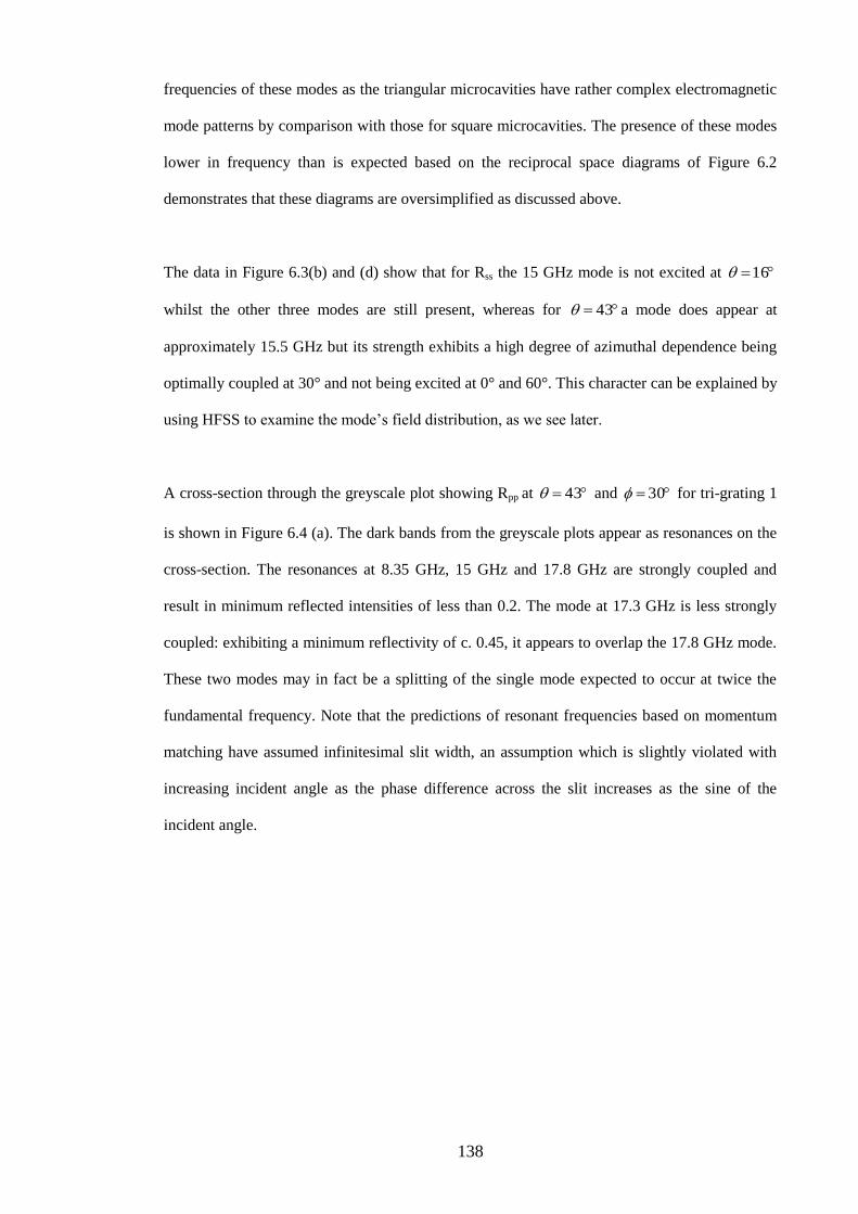
138
frequencies of these modes as the triangular microcavities have rather complex electromagnetic
mode patterns by comparison with those for square microcavities. The presence of these modes
lower in frequency than is expected based on the reciprocal space diagrams of Figure 6.2
demonstrates that these diagrams are oversimplified as discussed above.
The data in Figure 6.3(b) and (d) show that for Rss the 15 GHz mode is not excited at 16
whilst the other three modes are still present, whereas for 43 a mode does appear at
approximately 15.5 GHz but its strength exhibits a high degree of azimuthal dependence being
optimally coupled at 30° and not being excited at 0° and 60°. This character can be explained by
using HFSS to examine the mode’s field distribution, as we see later.
A cross-section through the greyscale plot showing Rpp at 43 and 30 for tri-grating 1
is shown in Figure 6.4 (a). The dark bands from the greyscale plots appear as resonances on the
cross-section. The resonances at 8.35 GHz, 15 GHz and 17.8 GHz are strongly coupled and
result in minimum reflected intensities of less than 0.2. The mode at 17.3 GHz is less strongly
coupled: exhibiting a minimum reflectivity of c. 0.45, it appears to overlap the 17.8 GHz mode.
These two modes may in fact be a splitting of the single mode expected to occur at twice the
fundamental frequency. Note that the predictions of resonant frequencies based on momentum
matching have assumed infinitesimal slit width, an assumption which is slightly violated with
increasing incident angle as the phase difference across the slit increases as the sine of the
incident angle.
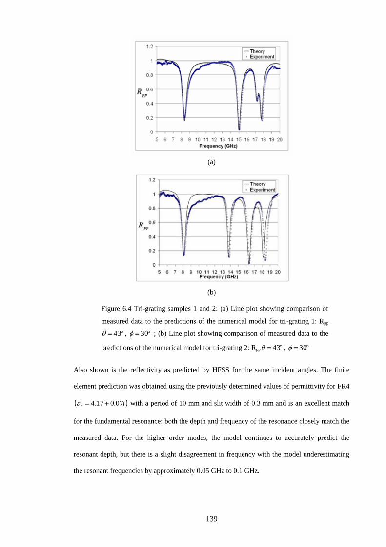
139
(a)
(b)
Figure 6.4 Tri-grating samples 1 and 2: (a) Line plot showing comparison of
measured data to the predictions of the numerical model for tri-grating 1: Rpp
43 , 30 ; (b) Line plot showing comparison of measured data to the
predictions of the numerical model for tri-grating 2: Rpp 43 , 30
Also shown is the reflectivity as predicted by HFSS for the same incident angles. The finite
element prediction was obtained using the previously determined values of permittivity for FR4
ir 07.017.4 with a period of 10 mm and slit width of 0.3 mm and is an excellent match
for the fundamental resonance: both the depth and frequency of the resonance closely match the
measured data. For the higher order modes, the model continues to accurately predict the
resonant depth, but there is a slight disagreement in frequency with the model underestimating
the resonant frequencies by approximately 0.05 GHz to 0.1 GHz.

140
Note also from both parts of Figure 6.4 that the model predicts a reflectivity greater than unity
at low frequencies: typically below 7 GHz and significantly higher than that measured between
9 GHz and 12 GHz. The former feature is obviously non-physical and indicates an error in the
model. Several modifications to the mesh were made but although the magnitude of the error
was reduced it could not be eliminated. This error is likely to be a consequence of the non-
orthogonal faces of the unit cell walls combined with the lower frequency excitation resulting in
a longer wavelength and thus reducing the relative spacing between the periodic boundaries.
The mismatch between theory and experiment between 9 GHz and 12 GHz is more likely a
consequence of normalisation errors during the measurement than a problem with the model.
HFSS has been used to plot the electric field vector on the upper surface of the lower metal
layer of tri-grating 1 at the resonant frequencies of: 8.35 and 15 GHz for 43 and 90
in Figure 6.5 (note that due to the hexagonal symmetry of the structure, 90 is equivalent
to 30 , 30 etc).
In Figure 6.5(a) the incident wave has a frequency of 8.35 GHz and is p-polarised having an
electric field component parallel to the y-axis: this results in a resonant mode with a field pattern
that is similar to that of the half-wavelength modes supported by the bi-grating and with regions
of strongest field along the edges of the patches which are parallel to the y-axis. An 8.35 GHz,
s-polarised incident wave also results in a half-wave resonance, with a field distribution again
determined by the direction of the electric field, which is parallel to the x-axis, see Figure
6.5(b). For both the p-polarised and s-polarised incident waves, coupling to these half-wave
modes is due to Bragg scattering associated with the reciprocal lattice points: (1, 0), (1, 1), (0,
1), (-1, 0), (-1, -1), (0, -1) which lie at kg from the origin.
Figures 6.5(c) and (d) show the electric field vector at 15 GHz for waves p-polarised and s-
polarised respectively. In both cases resonant modes are excited in which the anti-nodes appear
at and mid-way between, the corners of the triangular patches: however, in neither case are the

141
strongest fields confined to the sides of the patches that are parallel to the y-axis. In contrast to
the mode at 8.35 GHz, the fields appear to be approximately equal in strength along all edges,
indicating that rather than a regular one-wavelength mode, this is a coupled mode resulting from
scattering associated with the reciprocal lattice points: (2, 1), (1, 2), (-2, 1), (-2, -1), (-1, -2), (1, -
1) which lie at 3gk from the origin. These modes are the direct analogue of the {1, 1} coupled
modes supported by the bi-grating. (Note that the parentheses {} denote a set of modes whereas
the regular parentheses () denote an individual mode).
(a) (b)
(c) (d)
Figure 6.5 Tri-grating sample 1: predictions of the electric field vector
distribution at phases corresponding to peak field strengths on the upper
surface of the lower metal layer for: (a) an 8.35 GHz, p-polarised wave
incident at 43 90 ; (b) an 8.35 GHz, s-polarised wave incident at
43 90 ; (c) a 15 GHz, p-polarised wave incident at
43 90 ; (d) a 15 GHz, s-polarised wave incident at
43 90 , the longest arrows correspond to enhancements of 15 times
in all cases
142
For s-polarisation, the antinodes at the vertices of one triangle are half a cycle out of phase with
those at the vertices of the other triangle: the charge accumulations are of opposite sign. To
couple to the 15 GHz mode, the electric field of the incident wave must create this charge
distribution: see Figure 6.6(a). However, for s-polarisation, at 60,0,60 etc the electric
field lies parallel to one of the sets of slits. In Figure 6.6 (b) 60 for example, it is parallel
to the slit between the two triangles shown. The electric field of the incident s-polarised wave is
in-phase everywhere along this slit, therefore the charge accumulations at adjacent vertices of
the two triangles will be the same. Upon rotation in azimuth through another 60 the electric
field will be in-phase everywhere along the next set of slits and owing to the 60 rotational
symmetry of the structure this same behaviour will occur every 60 , hence this mode cannot be
excited at 60,0,60 etc as shown by the greyscale plot of Figure 6.3(d). The formation of
this charge distribution requires a difference in the phase of the incident electric field across the
unit cell. For small incident angles there is only a very small phase difference leading to weak
coupling, hence the mode is visible at 43 incidence but is not visible at 16 incidence.

143
(a)
(b)
Figure 6.6 Diagrams showing the incident electric field and resulting charge
distribution for a 15 GHz s-polarised wave incident at (a) 90 ; (b)
60
The higher order resonant modes between 17 and 18 GHz are associated with the (2, 0), (2, 2),
(0, 2), (-2, 0), (-2, -2), (0, -2) reciprocal lattice points which lie at 2kg from the origin. The
electric field vector has been plotted on the upper surface of the lower metal layer at the
resonant frequencies of: 17.3 and 17.8 GHz for a p-polarised wave incident at 43 and
60 in Figures 6.7(a) and (b) respectively. It is apparent that the field distribution of the
two modes is very similar which again indicates that this is in fact a splitting of one mode.

144
(a)
(b)
Figure 6.7 Tri-grating sample 1: predictions of the electric field vector
distribution at phases corresponding to peak field strengths on the upper
surface of the lower metal layer for: (a) an 17.3 GHz, p-polarised wave
incident at 43 , 90 ; (b) a 17.8 GHz, p-polarised wave incident
at 43 , 90 , the longest arrows correspond to enhancements of 15
times in both cases
6.4.2 Tri-grating sample 1 – polarisation conversion
Shown in Figure 6.8 are greyscale contour plots containing polarisation conversion intensity
data for tri-grating sample 1.

145
(a) (b)
(c) (d)
Figure 6.8 Experimental polarisation-converted reflected intensities for tri-
grating sample 1 shown as greyscale plots (a) Rps data as a function of
frequency and azimuthal angle at º16 (b) Rsp data as a function of
frequency and azimuthal angle at º16 (c) Rps data as a function of
frequency and azimuthal angle at º43 (d) Rsp data as a function of
frequency and azimuthal angle at º43
At the lower incident angle there is no discernable conversion occurring for either configuration.
Noise is apparent particularly between 10 GHz and 12 GHz and appears as a grey speckled
pattern. All plots feature a white line at 10 GHz, this is simply due to a discontinuity in the data:
two data sets were taken using two sets of antennas, one from 5 GHz to 9.98 GHz, the other
from 10 GHz to 20 GHz, hence there is a small gap between them. All plots also exhibit another
narrowband feature at 19.2 GHz. This is due to a resonance inherent to the system set-up: the
horn antennas used for 10 GHz – 20 GHz are technically only valid for use at frequencies up to
18 GHz: at 19.2 GHz the antennas support a higher order mode which appears as a resonance,

146
the magnitude of which is reduced by normalisation but becomes more apparent here since the
scale has been so greatly expanded.
The higher incident angle does exhibit very low levels of conversion – no more than 2%. This
conversion is produced by the higher order (2, 0), (2, 2), (0, 2), (-2, 0), (-2, -2) and (0, -2)
modes. The conversion appears as two distinct features, one centred on 13° the other on 42°.
With reference to Figure 6.1(a), at 0° azimuth the incident electric field is perpendicular to one
set of slits (that parallel to the y-axis) and at 30° to the other two sets. Upon rotation to 15° the
electric field vector is then at 45° to one set of slits. By analogy to the mono- and bi-gratings,
when the vector is at 45° to the slit this constitutes the best compromise between coupling to
and from the mode to and from p- and s-polarisation, and hence conversion is a maximum. Due
to the hexagonal symmetry of the tri-grating the electric field vector is at 45° to one set of slits
every 30° of rotation, hence the polarisation conversion intensity is periodic with respect to
azimuth, with the period being 30°. That the features occur 2° lower in azimuth than expected is
due to slight errors in the experimental set-up: the sample was not quite aligned with one sets of
slits parallel to the y-axis when the rotation began.
6.4.3 Tri-grating sample 2
The greyscale plots of Figure 6.9 show the specular (a) Rpp and (b) Rss reflected intensities from
the tri-grating 2 sample. The data are plotted as a function of frequency and azimuthal angle
with 16 . Figure 6.9(c) and (d) again show Rpp and Rss respectively for tri-grating sample 2
but with 43 . Shown in Figure 6.9(e) and (f) are the Rpp and Rss data respectively for tri-
grating sample 1 with 43 - these have been shown again here to facilitate a comparison of
the responses of the two samples.
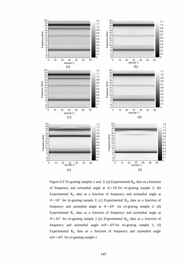
147
(a) (b)
(c) (d)
(e) (f)
Figure 6.9 Tri-grating samples 1 and 2: (a) Experimental Rpp data as a function
of frequency and azimuthal angle at 16 for tri-grating sample 2; (b)
Experimental Rss data as a function of frequency and azimuthal angle at
16 for tri-grating sample 2; (c) Experimental Rpp data as a function of
frequency and azimuthal angle at 43 for tri-grating sample 2; (d)
Experimental Rss data as a function of frequency and azimuthal angle at
43 for tri-grating sample 2 (e) Experimental Rpp data as a function of
frequency and azimuthal angle at 43 for tri-grating sample 1; (f)
Experimental Rss data as a function of frequency and azimuthal angle
at 43 for tri-grating sample 1

148
The dark bands at 8.1 GHz, 13.8 GHz, 16.4 GHz and 18.3 GHz in Figure 6.9(a) and (c) indicate
strong absorption. The fundamental 8.1 GHz mode exhibits a high degree of azimuthal
invariance, whereas the first harmonic (the mode at 13.8 GHz) shifts to slightly higher
frequencies upon rotation towards 30 azimuth. As the grating is rotated the component of in-
plane momentum in the direction of propagation of the mode changes, hence the frequency
shifts to satisfy momentum conservation. The 16.4 GHz mode also exhibits some azimuthal
variation, shifting towards lower frequencies on rotation towards 30 azimuth. At 43 the
highest frequency mode appears to split with two azimuthally dependant modes appearing
between 17.5 GHz and 18.7 GHz.
Both the measured data and the HFSS model demonstrate that the fundamental mode for tri-
grating 2 occurs slightly lower in frequency than that of tri-grating 1 despite both samples
having identical repeat periods and material properties: see Figures 6.3, 6.4 and 6.9. This
indicates that in addition to the repeat period of the slits, the off-set between the sets of slits and
therefore the size and shape of the patches, also affect the resonant frequencies, as was
highlighted previously during the discussion of the grating profile and its Fourier components.
As expected on the basis of momentum conservation, the higher order modes occur at
frequencies which approximate simple multiples of the fundamental: the ratio of 13.8 GHz to
8.1 GHz is 1.70, which is very close to 3 ; the ratio of 16.4 GHz to 8.1 GHz is 2.02, which is
close to 2. However, the next mode is expected to occur at 7 times the fundamental frequency,
approximately 21.4 GHz, whereas modes are observed at 17.5 GHz and 18.7 GHz.
The data in Figure 6.9(b) and (d) show that for Rss the 16.4 GHz mode is not excited for
either 16 or 43 , this can again be explained by considering the field distribution of the
mode. The other three modes are still present and occur at: 8.1 GHz, 13.8 GHz and 18.3 GHz as
for p-polarisation. The fundamental demonstrates azimuthal invariance, whereas the first
harmonic mode exhibits behaviour similar to that for p-polarisation, except that it shifts down in

149
frequency rather than up upon rotation towards 30 azimuth: this effect is very subtle but can be
discerned by viewing the plots from the side at a grazing angle. For this mode, rotation towards
30 azimuth increases the component of in-plane momentum in the direction of the mode;
hence there is a shift down in frequency to off-set this increase. Another mode appears at 17.2
GHz and is highly sensitive to azimuth, being optimally coupled at 0 and 60 azimuth, and
not being excited at 30 azimuth. The 18.3 GHz mode remains largely stable in frequency with
only a minor shift down upon rotation to 30 azimuth.
Comparing the greyscale plot of Figure 6.9(c) to that of Figure 6.9(e) and similarly part (d) to
part (f), reveals the striking differences in the structure of the higher frequency modes. The
greyscales plots for tri-grating sample 1 exhibit a more complex, more intricate structure than
those of tri-grating sample 2. This demonstrates very clearly the effect of the extra Fourier
components.
A cross-section through the greyscale plot showing Rpp at 43 and 30 for tri-grating 2 is
shown in Figure 6.4 (b). The dark bands from the greyscale plots appear as resonances in this
cross-section. All four resonances are strongly coupled and result in minimum reflectivities of
less than 0.2. Also shown is the reflectivity as predicted by HFSS for the same incident angles.
The model predicts the frequency and depth of the fundamental resonance very accurately: for
the higher order modes, the model continues to accurately predict the resonant depth, but there
is a slight disagreement in frequency with the model underestimating the resonant frequencies
by approximately 0.05 GHz to 0.2 GHz.
HFSS can be used to examine the field distribution of the modes shown in Figures 6.4 and 6.9:
it has been used to plot the electric field vector on the upper surface of the lower metal layer of
tri-grating 2 at the resonant frequencies of 8.1 and 13.8 GHz for 43 and 60 in Figure
6.10. In Figure 6.10(a) the incident wave has a frequency of 8.1 GHz and is p-polarised: the
region beneath the central hexagon supports a half-wave resonant mode. 8.1 GHz s-polarised
radiation incident at the same angle also excites a half-wave mode beneath the hexagonal patch,

150
although the mode appears transverse to the plane of incidence due to the polarisation of the
incident wave, see Figure 6.10(b). For both the p-polarised and s-polarised incident waves,
coupling to these half-wave modes is due to Bragg scattering associated with the reciprocal
lattice points: (1, 0), (1, 1), (0, 1), (-1, 0), (-1, -1), (0, -1) which lie at kg from the origin.
Figures 6.10(c) and (d) show the electric field vector at 13.8 GHz for waves p-polarised and s-
polarised respectively: both polarisations excite modes in which there are field anti-nodes on
opposing sides of the central hexagon which are in-phase with each other. Half-wavelength
modes would exhibit antinodes that were half a cycle out of phase with each other, and
wavelength modes would require an additional anti-node in the centre of the hexagon.
Furthermore, in accordance with momentum conservation, wavelength modes would be
expected to occur at twice the fundamental frequency. Therefore, the field plots in Figures 6.10
(c) and (d) do not show degenerate one-wavelength modes but rather coupled modes that result
from scattering associated with any of the following reciprocal lattice points: (2, 1), (1, 2), (-2,
1), (-2, -1), (-1, -2), (1, -1) which lie at 3gk from the origin, as was shown to be the case for
tri-grating sample 1.

151
(a) (b)
(c) (d)
Figure 6.10 Tri-grating sample 2: predictions of the electric field vector
distribution at phases corresponding to peak field strengths on the upper
surface of the lower metal layer for: (a) an 8.1 GHz, p-polarised wave incident
at 43 , 60 ; (b) a 8.1 GHz, s-polarised wave incident at
43 , 60 ; (c) a 13.8 GHz, p-polarised wave incident at 43 ,
60 ; (d) a 13.8 GHz, s-polarised wave incident at 43 , 60 , the
longest arrows correspond to enhancements of 15 times in all cases
Shown in Figure 6.11 (a) is a plot of the electric field vector for a 16.4 GHz p-polarised wave
incident at 43 , 60 . The fields are again confined to the region beneath the hexagon
and exhibit a one-wavelength resonance: the anti-node at the centre of the hexagon is half a
cycle out of phase with that which appears around the perimeter. That there appears to be an
anti-node around the entire perimeter of the hexagon, indicates that degenerate modes are

152
excited at these incident angles due to simultaneous scattering associated with two or more the
lattice points located at 2kg from the origin.
(a)
(b) (c)
Figure 6.11 Tri-grating sample 2: (a) prediction of the electric field vector
distribution at a phase corresponding to peak field strength on the upper
surface of the lower metal layer for: a 16.4 GHz, p-polarised wave incident at
43 , 60 ; (b) diagram showing the incident electric field and
resulting charge distribution for a p-polarised wave incident at 90 ; (c)
diagram showing the incident electric field and resulting charge distribution for
a s-polarised wave incident at 90
The excitation of this mode for p-polarisation is possible as the phase change across the patches
causes a reversal of the direction of the electric field and the resulting components of the electric
field drive charges of like sign towards the centre of the hexagon; see Figure 6.11(b). However,
it is not possible to create this charge distribution with s-polarisation at any azimuth because the
components of the electric field do not drive like charges towards the centre Figure 6.11(c).

153
Plots of the electric field vector for modes excited by an s-polarised wave incident at
43 , 60 for frequencies of 17.1 GHz and 18.3 GHz are shown in Figures 6.12(a) and
(b) respectively, these modes are associated with the (2, 0), (2, 2), (0, 2), (-2, 0), (-2, -2), (0, -2)
reciprocal lattice points which lie at 2kg from the origin. It is apparent that the field distribution
of the two modes is similar, however that for 18.3 GHz, Figure 6.12(b), appears to show a
mode confined to region beneath the triangular patch with very little excitation of any mode
under the much large hexagonal patch. The field distribution appears similar to that of the
fundamental modes of tri-grating sample 1 which featured only triangular patches. This may
therefore be the fundamental mode for the small triangle.
(a) (b)
Figure 6.12 Tri-grating sample 2: (a) prediction of the electric field vector
distribution at a phase corresponding to peak field strength on the upper
surface of the lower metal layer for: a 17.1 GHz, s-polarised wave incident at
43 , 60 ; (b) prediction of the electric field vector distribution at a
phase corresponding to peak field strength on the upper surface of the lower
metal layer for: a 18.3 GHz, s-polarised wave incident at 43 , 60
6.4.4 Tri-grating sample 2 – polarisation conversion
Shown in Figure 6.13 are greyscale contour plots containing polarisation conversion intensity
data for tri-grating sample 2.
As with tri-grating sample 1, the lower incident angle does not produce any measurable
polarisation conversion. However, the higher incident angle does exhibit more significant levels
of conversion: up to 8% for both configurations. In this case it is the: (2, 1), (1, 2), (-2, 1), (-2, -
1), (-1, -2), (1, -1) modes which support conversion. Again the polarisation-converted intensity
is periodic with respect to azimuth due to the hexagonal symmetry of the sample.
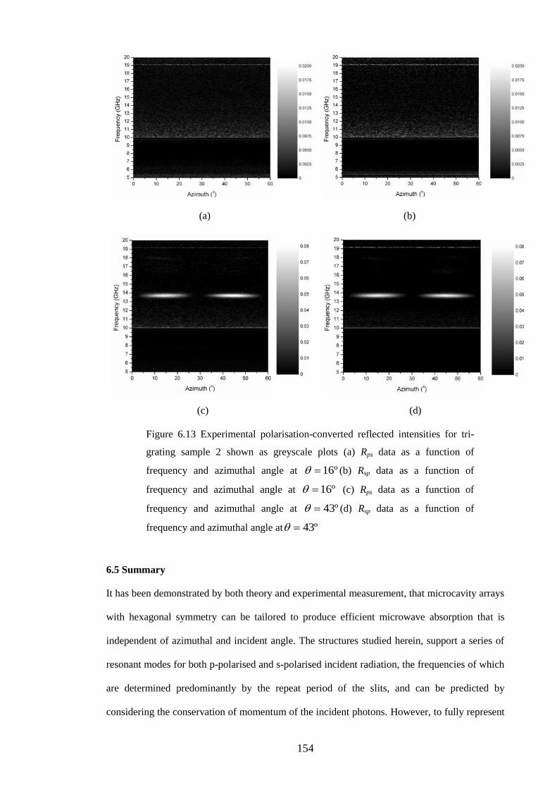
154
(a) (b)
(c) (d)
Figure 6.13 Experimental polarisation-converted reflected intensities for tri-
grating sample 2 shown as greyscale plots (a) Rps data as a function of
frequency and azimuthal angle at º16 (b) Rsp data as a function of
frequency and azimuthal angle at º16 (c) Rps data as a function of
frequency and azimuthal angle at º43 (d) Rsp data as a function of
frequency and azimuthal angle at º43
6.5 Summary
It has been demonstrated by both theory and experimental measurement, that microcavity arrays
with hexagonal symmetry can be tailored to produce efficient microwave absorption that is
independent of azimuthal and incident angle. The structures studied herein, support a series of
resonant modes for both p-polarised and s-polarised incident radiation, the frequencies of which
are determined predominantly by the repeat period of the slits, and can be predicted by
considering the conservation of momentum of the incident photons. However, to fully represent

155
the detailed shape of the grating profile requires that higher order Fourier components be
considered. These components are responsible for the otherwise unexpected differences
between the structure of higher order modes for the two tri—grating samples.
These microcavity absorbing structures could be applied to reduce the level of backscattered
radiation in environments where the direction and polarisation of incident radiation is varying or
unpredictable. Examples of such environments include: airports where reflections from
buildings can cause significant interference problems and the interior of buildings where
screening from electromagnetic radiation is required. Furthermore, the thin, flexible and
lightweight nature of the material makes it ideal for EMC (Electromagnetic Compatibility)
applications where space is critical such as on or within the housing of sensitive instruments.

156
Chapter 7
Methods for achieving maximum absorption bandwidth
7.1 Introduction
The preceding experimental chapters have demonstrated that ultra-thin microcavity arrays offer
a novel approach for the control and in particular the absorption of microwave radiation.
However, the results hitherto presented feature narrow resonances which only absorb efficiently
over a very limited range of frequencies. This chapter constitutes efforts to increase the
absorption bandwidth of the microcavity array structures. To this end, the absorption bandwidth
of a series of optimised microcavity array absorbers is studied and compared to theoretical
expectations based on cavity thickness and magnetic permeability. It is found that even basic
microcavity array structures, when optimised, afford absorption bandwidths that exceed 90% of
the theoretical limit. By introducing a multiplicity of cavity configurations including multiple-
period, multiple-permittivity and multiple-layer designs, total absorption bandwidth is increased
slightly and greater control over the frequency distribution of the absorption is obtained.
One of the greatest challenges in the design of absorbing materials, is the bandwidth-to-
thickness ratio. The work of Brewitt-Taylor (1999, 2007) and that of Rozanov (2000) has
demonstrated that there is a fundamental limit on the maximum absorption bandwidth that can
be achieved from a material, and that this limit depends on the thickness of the material and its
magnetic permeability. The primary consequence of this is that a given material can only exhibit
efficient absorption over a finite range of frequencies and that outside of this range the material
will not absorb efficiently.
The purpose of this chapter is to compare the total bandwidth product of the microcavity arrays
to the theoretical limits based on thickness and permeability, and to present four strategies for
maximising the total absorption bandwidth. These four strategies are embodied in the
microcavity array structures presented herein, and can be summarised as:
Multiple discrete repeat periods
Multiple continuous repeat periods

157
Multi-layering
Multiple permittivities
7.2 Experimental
The experimental co-ordinate system and structure geometries are shown in Figure 7.1. The
structures are formed from various thicknesses of non-magnetic (i.e. μr = 1) dielectric materials
including: FR4 PCB (printed circuit board) made from laminated glass cloth infused with resin,
polyester (PET) sheet, alumina (Al2O3) and air, bounded top and bottom by 18 μm thick copper
layers. The dimensions of the structures are as annotated in Figure 7.1. In all cases the slits have
a width of 0.3 mm, being formed using standard print and etch techniques (Eurotech); all
structures measure 450 mm by 450 mm. Their reflectivity at normal incidence was measured
over 5.4 GHz to 18 GHz (55.6 mm to 16.7 mm wavelength) using the focused horn apparatus
as detailed in Chapter 4. In all cases the electric field vector of the incident radiation was
orientated perpendicular to the slits.
Structure 1 is a combination of two repeat periods (inter-slit distances): L1 = 10 mm and L2 = 9
mm giving a total repeat period of 19 mm. All slits run parallel to the y-axis and perpendicular
to the electric field of the incident wave: see Figure 7.1(c). In Structure 2, every other slit has a
saw-toothed shape, the period of the saw-tooth being 40 mm and its amplitude being 2 mm.
Thus the distance between adjacent slits varies from 8 mm to 12 mm and back to 8 mm every 40
mm along the y-axis, see Figure 7.1(d). Successive saw-tooth slits are half a period out of phase
with each other, thus making the overall period of the structure 40 mm in the x-direction. In
Structures 1 and 2, the dielectric core material is FR4 with complex permittivity εr =4.17 + 0.07i
as detailed in Chapter 4.
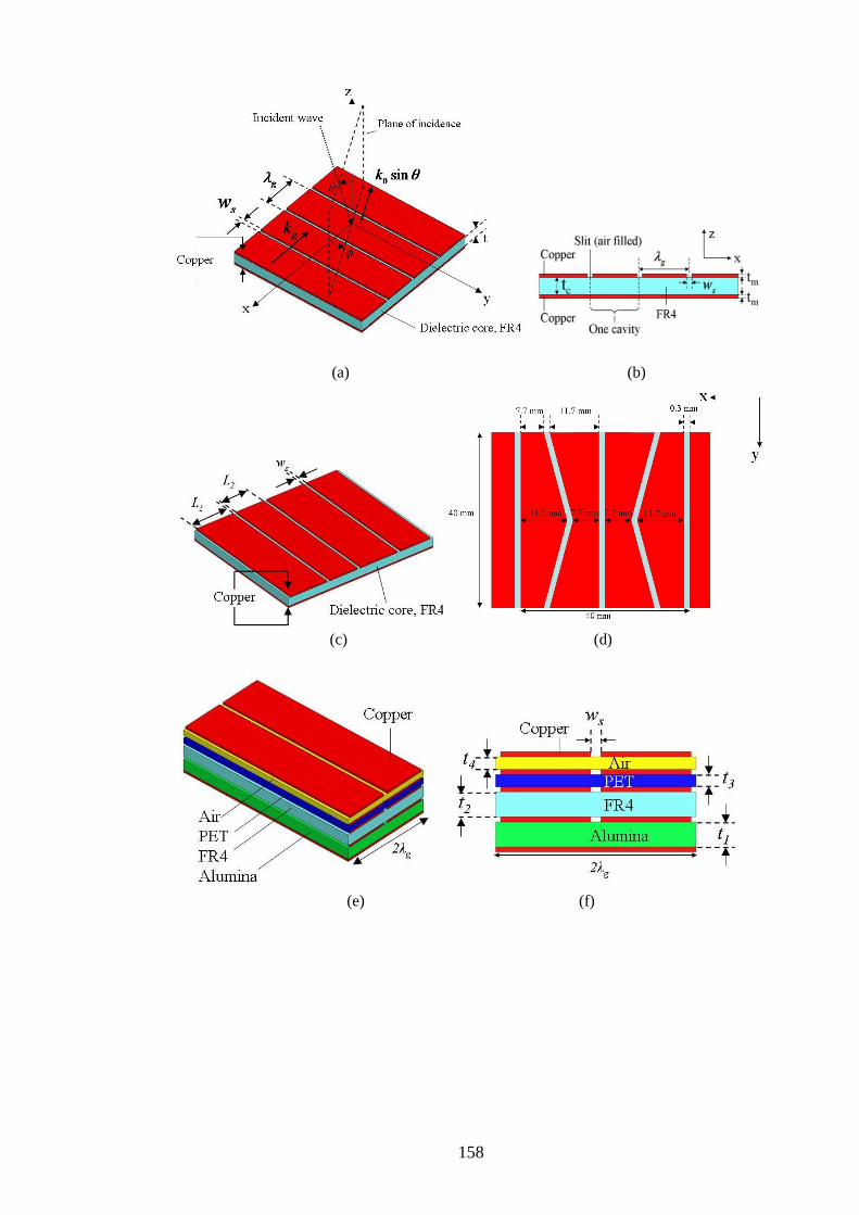
158
(a) (b)
(c) (d)
(e) (f)

159
(g)
Figure 7.1 The microcavity structure geometries (not to scale) and the co-
ordinate system used: θ is the incident angle, is the azimuthal angle, ws is
the slit width, g is the repeat period of the structure (a) 3-D projection of a
standard mono-grating structure in which all slits run parallel (b) Cross-section
through the standard mono-grating structure (c) 3-D projection of Structure 1,
multiple discrete repeat periods (d) Plan view projection of Structure 2,
multiple continuous repeat periods with alternate saw-tooth slits (e) 3-D
projection of Structure 3, multi-layer structure, 2 periods shown (f) end
projection of Structure 3, multi-layer structure, 2 periods shown (g) 3-D
projection of Structure 4, multiple refractive indices
Structure 3 consists of 4 layers each with a period of 10 mm and slit width of 0.3 mm, but with
differing material properties and thicknesses. The four layers are stacked one upon the other
such that their slits are aligned: the top three layers have slits in both copper layers to allow
penetration of the incident wave to the lower layers, see Figure 7.1(e) and (f). Due to the
complexity of this structure, the high probability of inter-layer misalignment, and consequent
distortion of results, fabrication of a physical sample was not undertaken. Instead HFSS was
used to simulate its performance. The complex permittivities of PET and alumina are εr = (3.2 +
0.0096i) and εr = (9.4 + 0.0564i) respectively and were obtained from the database within
HFSS.
Structure 4 has a fixed period of 20 mm, each period containing two slits spaced apart by 10
mm and both having widths of 0.3 mm, the properties of the core material alternate between
adjacent cells. In the first cell the core material has a complex permittivity of εr1 =3.5 + i0.07, in

160
the second unit cell the complex permittivity is εr2 = 4.17 + i0.07, see Figure 7.1(g). Again due
to the complexity of fabrication HFSS was used to simulate the performance of this structure.
7.3 Theory
Work by Bode (1945) and later work by Fano (1950) demonstrated that there is a fundamental
limit to the bandwidth over which a source impedance can be matched to a load impedance
within an electrical circuit. Both Brewitt-Taylor (1999, 2007) and Rozanov (2000) have applied
this work to the field of absorbing materials and demonstrated that there is a limit to the
maximum absorption bandwidth which is determined by the material’s thickness and
permeability.
Rozanov (2000) formulates the bandwidth-to-thickness relationship in terms of wavelength,
whereas Brewitt-Taylor’s (1997) formula is written in terms of frequency. Both formulations
use reflectivity in decibels and describe a limit to the area beneath the curve on a plot of
reflectivity in decibels versus wavelength or frequency respectively, see Figure 7.2.
Figure 7.2 Response of an example Salisbury screen absorber as predicted
using the finite element model (a) reflectivity in decibels versus frequency (b)
reflectivity in decibels versus wavelength

161
For a Salisbury screen (Knott et al (1993) and Salisbury (1952)) in which all the constituent
materials have unity permeability, the result due to Brewitt-Taylor (1999) is:
0 00 10ln
3201
hdffR
fdB (7.1)
Where:
RdB is the reflectivity in decibels
f0 is the centre frequency of the absorption band
λ0 is the centre wavelength of the absorption band
h is the thickness of the spacer within the Salisbury screen
Note that this formula applies to structures illuminated by plane waves at normal incidence and
considers only the lowest-frequency absorption band. This latter restriction is a consequence of
performing the integral over frequency, in which regime results an infinite series of absorption
bands and hence an infinite integral, see Figure 7.2. In a more recent publication Brewitt-Taylor
(2008) extends this concept to determine the bandwidth limits on magnetic conductor surfaces
at oblique incidence.
Rozanov (2000) presents the following formula for broadband absorbers:
iiiidB hhdR
17210ln
40 2
0
(7.2)
Where:
μi is the relative magnetic permeability of the ith
layer at zero frequency
hi is the thickness of the ith layer
and all other terms have the same meaning as in (7.1).
In the case of narrowband absorbers, Rozanov (2000) presents an alternative formula:
iiiidB hhdR 13910ln
320
0
(7.3)

162
In this case, a narrowband absorber is one in which 1.00 , where is the operating
bandwidth. It can be shown that the narrowband limit (7.3) is equivalent to (7.1) and as such
applies only to the lowest-frequency absorption band. Taking the ratio of (7.3) to (7.2) returns a
value of 0.81 (to 2 d.p.) indicating that the lowest frequency absorption band accounts for no
more than 81% of the total bandwidth. Typical values for 0 for the microcavity absorbers,
are < 0.05 (see preceding chapters) which classifies them as narrowband, therefore their total
absorption bandwidth has been compared to the narrowband limit (7.3). Note that the
formulations (7.1) - (7.3) all exclude the thickness of the ground plane or lowermost metal
layer.
The microcavity array structures support a series of standing-wave modes similar to the Fabry-
Perot resonances of a metallic slit (Takakura (2001)), the frequencies of which, fN, are given by
(7.4):
nL
Ncf N
2 (7.4)
Where:
fN is the frequency of the Nth order Fabry-Perot mode
c is the speed of light in vacuum
n is the refractive index of the dielectric material within the cavity
L is the length of the cavity
N is a positive integer
As was demonstrated in Chapter 4, the incident angle θ and the azimuthal angle , influence
which modes the mono-grating microcavity structure will support, for example: at normal
incidence the structure will support only those modes where N is odd, whereas off-normal the
grating can also support the modes where N is even. Additional modes will increase the total
absorption bandwidth, however, this is not useful when considering the limits (7.2) and (7.3)
since this applies only to structures illuminated at normal incidence. Note also that upon rotation

163
away from º0 and θ = 0°, the resonant frequencies given by (7.4) become increasingly
inaccurate. In such cases the resonant frequencies can be found by considering the momentum
of the incident photons, details can be found in Chapter 5.
From (7.4) it can be seen that the two factors which determine the frequencies of the series of
modes are the slit-spacing L and the refractive index n. By introducing a multiplicity of slit
spacings, and/or refractive indices, multiple series can be excited with the potential of
increasing the overall absorption bandwidth.
7.4 Results
The total absorption bandwidth for each structure studied, was calculated by dividing the area
beneath the 0 dB line into a series of trapezia and finding their individual areas, the sum of these
giving the total area under the curve to a good approximation. The total bandwidth product of
each structure is compared both to the theoretical limit (7.3) and to that afforded by the
standard, single layer mono-grating with an FR4 core, period, λg, of 10 mm and slit width ws of
0.3 mm, see Figure 7.1(a).
7.4.1 Standard mono-grating
The reflectivity of the standard mono-grating in decibels versus wavelength both as measured
experimentally and predicted by the finite element model, is shown in Figure 7.3(a) for
radiation incident normally and with its electric field vector perpendicular to the slits. There is
excellent agreement between the two datasets both exhibiting a deep resonance at 43.7 mm (6.9
GHz). From (7.4) it is apparent that this resonance is the mode for N = 1: the N = 2 mode is not
excited at normal incidence (see Chapter 4) and the N = 3 mode lies just above 20 GHz (15 mm
wavelength) and is therefore inaccessible using this measurement set-up. The total bandwidth
products for the experimental and theoretical datasets are 23.4 dBmm and 24.4 dBmm
respectively, equating to 45% and 47% of the narrowband limit (7.3).

164
(a)
(b)
(c)
Figure 7.3 Theoretical and experimental data for standard mono-grating (a)
Reflectivity in decibels versus wavelength as predicted by the finite element
model and measured experimentally (b) Reflectivity in decibels versus
wavelength as predicted by the finite element model for mono-grating
structures of differing core thickness (c) Percent of narrowband bandwidth
limit versus core thickness for the a series of mono-grating structures

165
The experimental microcavity structure was fabricated from an available thickness of FR4: tc =
356 μm. This does not necessarily constitute an optimum structure or therefore the maximum
possible absorption bandwidth. By altering the FR4 thickness using HFSS the depth of the
resonance can be maximised and the largest absorption bandwidth obtained.
Shown in Figure 7.3(b) and (c) are the results of varying the FR4 thickness, tc, in the HFSS
model: as tc is decreased from 356 μm, the resonance becomes deeper and shifts to shorter
wavelengths and maximum absorption depth is achieved with a core 180 μm thick. This
structure affords the closest match between the non-radiative loss, arising from dissipation by
both the metal layers and the dielectric core, and the radiative loss, arising from re-radiation by
the cavity, and hence absorption depth is a maximum. This structure also exhibits the greatest
percentage absorption bandwidth: 25.6 dBmm equivalent to 92.9% of the narrowband limit
(7.3), see Figure 7.3(c).
As core thickness is decreased to less than 180 μm, resonance depth begins to decrease as does
the total absorption bandwidth. However, as the core thickness decreases so does the theoretical
bandwidth limit (7.3) hence the rate of percentage bandwidth decrease is relatively slow. Above
180 μm, the resonance becomes shallower, but this is off-set by an increase in the width of the
resonance. Overall, the total bandwidth product remains at approximately 25 dBmm for
thickness up to 356 μm, however since the value of (7.3) is increasing with core thickness the
percentage bandwidth decreases rapidly.
7.4.2 Structure 1 – multiple discrete repeat periods
The overall repeat period of this structure is 19 mm, comprising a 10 mm inter-slit distance
alternated with a 9 mm inter-slit distance. All slits are parallel to each other and are 0.3 mm
wide, the dielectric core material is FR4 with permittivity 4.17 + i0.07. The first structure
investigated had a core thickness 190 μm, see Figure 7.1(c). The reflectivity of this structure as
a function of wavelength is shown in Figure 7.4(a): this structure supports resonances at 41 mm
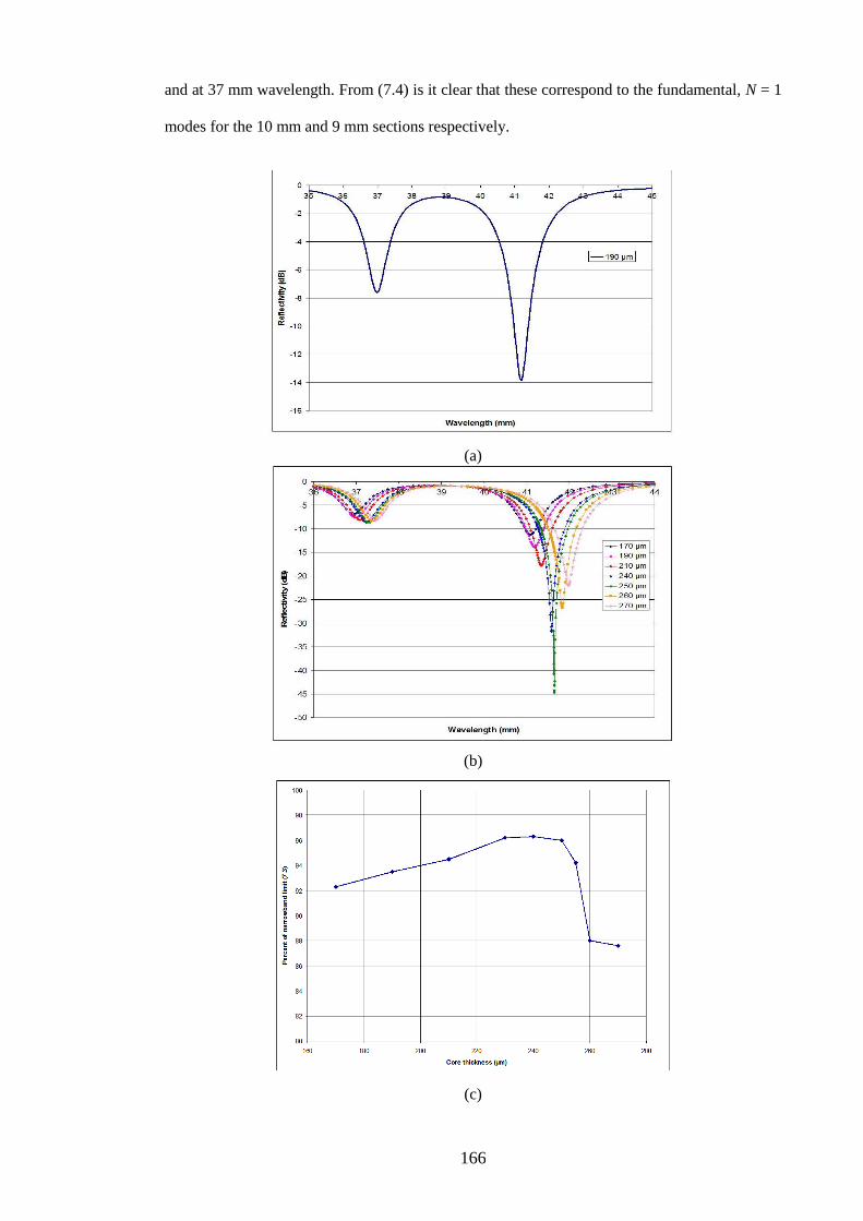
166
and at 37 mm wavelength. From (7.4) is it clear that these correspond to the fundamental, N = 1
modes for the 10 mm and 9 mm sections respectively.
(a)
(b)
(c)

167
(d)
(e)
Figure 7.4 Multiple discrete period structures (a) Reflectivity in decibels versus
wavelength for structure with dielectric core thickness of 190 μm (b)
Reflectivity in decibels versus wavelength as predicted by the finite element
model for multiple discrete period structures of differing core thickness (c)
Percent of narrowband bandwidth limit versus core thickness for the a series of
multiple discrete period structures (d) Cross-section of modified multiple
discrete repeat period structure, (e) Reflectivity in decibels versus wavelength as
predicted by the finite element model for multiple discrete period structures with
different values of t2
As with the standard mono-grating, the dielectric core thickness was varied in order to derive
the maximum absorption depth and maximum percentage bandwidth of (7.3). It can be seen
from Figure 7.4(b) that a core thickness of around 250 μm maximises the depth of the longer-
wavelength resonance. Upon close inspection, the depth of the shorter-wavelength resonance
changes in the same manner with greatest depth being reached at a core thickness of 250 μm,
but the magnitude of the change on a decibel scale is much smaller for this resonance.

168
A core thickness of 230 μm - 250 μm also produces optimum absorption bandwidth: this
structure achieves 96% of the narrowband limit (7.3) and therefore does constitute a small
improvement over the standard mono-grating. Note that the combined area of both resonances
has been summed in order to produce the 96% figure. The variation in absorption bandwidth
with core thickness is summarised in Figure 7.4(c): there is a gradual increase in percentage
bandwidth (7.3) up to 250 μm after which begins a much faster decline. For thicknesses greater
than 250 μm, the resonances are becoming shallower but the bandwidth limit (7.3) is
simultaneously increasing, hence the rate of decrease in the percentage bandwidth is large.
If the depth of both resonances could be simultaneously optimised, then overall absorption
bandwidth might be increased. To this end the thickness of the dielectric core within the 9 mm
long cavity, t2 in Figure 7.4(d), was progressively decreased from 240 μm to 180 μm, whilst the
thickness of the dielectric core within the 10 mm long cavity was fixed at 240 μm, the results of
this modification are shown in Figure 7.4(e). The depth of the shorter-wavelength resonance has
been increased beyond values seen with the previous structure, Figure 7.4(b), although it still
has not exceeded -10 dB. However, the longer-wavelength resonance has been perturbed and is
sensitive to any change in t2. The total absorption bandwidth has actually decreased. This is
because there has been a reduction in total absorbing volume: the fields are excluded from all
but top few microns of the metal and hence by decreasing, t2 the fraction of the total structure
volume available to absorb is reduced. Note also that this design creates an ambiguity as to what
value of h should be used in (7.3), making a determination of the percentage bandwidth very
difficult.
7.4.3 Structure 2 – multiple continuous repeat periods
In Structure 2, successive slits alternate between being straight and having saw-toothed shape.
The period of the saw-tooth slits is 40 mm and their amplitude is 2 mm. In this structure the
inter-slit distance varies from 8 mm to 12 mm and back to 8 mm every 40 mm along the y-axis,
refer to Figure 7.1(c). In Structure 2 the dielectric core material is FR4 with complex
permittivity εr =4.17 + 0.07i, the core thickness of the measured structure was 356 μm.

169
The experimentally measured reflectivity of this structure versus wavelength is compared to that
predicted by HFSS in Figure 7.5(a). There is good agreement between the two datasets: both
predict a deep resonant absorption at 47 mm and a number of shallower resonances at shorter
wavelengths. The HFSS model predicts that these shallower features occur at slightly shorter
wavelengths than those observed experimentally. This may be due to imperfections in the saw-
toothed slits of the experimental structure; around the vertex of the saw-tooth the accuracy
achievable with the etching process may be less than elsewhere on the structure.
Although by contrast to basic mono-grating, there are no simple numerical relationships for
predicting the resonant wavelengths of structures in which the slits are not parallel, on the basis
of (7.4) one might that the response of this structure would be a broad and possibly shallow
resonance lying between 6.1 and 9.2 GHz. However, instead a series of narrow resonances
result. This is further evidence that the simple approximation of (7.4) is indeed too simple.
Nevertheless, the nature of the resonant modes can be explored by using HFSS.
From Figure 7.5(d) it is apparent that the mode at 47 mm is a half-wave mode, the strength of
which varies in the x-direction: strongest at points where the inter-slit distance is 12 mm and
weakest at points where the inter-slit distance is 8 mm. Using a value for L of 12 mm in (7.4)
returns a resonant wavelength of 49 mm which is close to the 47 mm resonance observed. The
shorter wavelength modes have more complex field patterns which cannot readily be likened to
regular modes, nor do their resonant wavelengths correspond to any apparent period or inter-slit
distance of the structure – see Figure 7.5 (e) and (f). These complex field patterns are
reminiscent of modes supported by hexagonally symmetric microcavity structures studied in
Chapter 6 which also featured metal patches the sides of which were not everywhere
perpendicular.

170
(a)
(b)
(c)

171
(d)
(e) (f)
Figure 7.5 Multiple continuous period structures (a) Reflectivity in decibels
versus wavelength as predicted by the finite element model and measured
experimentally (b) Reflectivity in decibels versus wavelength as predicted by
the finite element model for multiple continuous period structures of differing
core thickness (c) Percent of narrowband bandwidth limit versus core thickness
for the a series of multiple continuous period structures (d) Plot of the
instantaneous electric field vector on the upper surface of the lower metal layer
at a wavelength of 47 mm and a phase corresponding to peak field, the longest
arrows correspond to 30 V/m (an enhancement of 30 times the incident field),
dashed lines added to indicate position of slits (e) Plot of the magnitude of the
instantaneous electric field on the upper surface of the lower metal layer at a
wavelength of 40 mm and a phase corresponding to peak field, dark blue areas
correspond to 0 V/m, green areas to 20 V/m (f) Plot of the magnitude of the
instantaneous electric field on the upper surface of the lower metal layer at a
wavelength of 36 mm and a phase corresponding to peak field, dark blue areas
correspond to 0 V/m, green areas to 20 V/m and red areas to 30 V/m

172
The dielectric core thickness was progressively decreased from 356 μm to 180 μm. As per
Structure 1, the optimum absorption depth and bandwidth occurs for a core thickness of 230 μm
to 250 μm: see Figures 7.5(b) and (c). For this core thickness, the structure achieves over 96%
of the narrowband limit (7.3): this level of performance is also very similar to that of Structure
1. Despite the additional modes being excited, the total absorption bandwidth still does not
exceed the limit set by (7.3).
7.4.4 Structure 3 - Multi-layering
HFSS was used to study the behaviour of the multi-layer structure shown in Figure 7.1(e) and
(f) with: t1 = 0.13 mm, t2 = 0.12 mm, t3 = 0.1 mm, t4 = 0.075 mm, the copper layers each had a
thickness of 0.018 mm giving a total thickness excluding the lowermost copper layer, of 0.497
mm. This structure’s reflectivity in decibels versus wavelength is shown in Figure 7.6(a). Over
the 15 mm to 70 mm (20 GHz to 4.29 GHz) range the structure supports five resonances, all of
which exhibit minimum reflectivities of less than -10 dB which corresponds to more than 90%
of the incident radiation being absorbed.
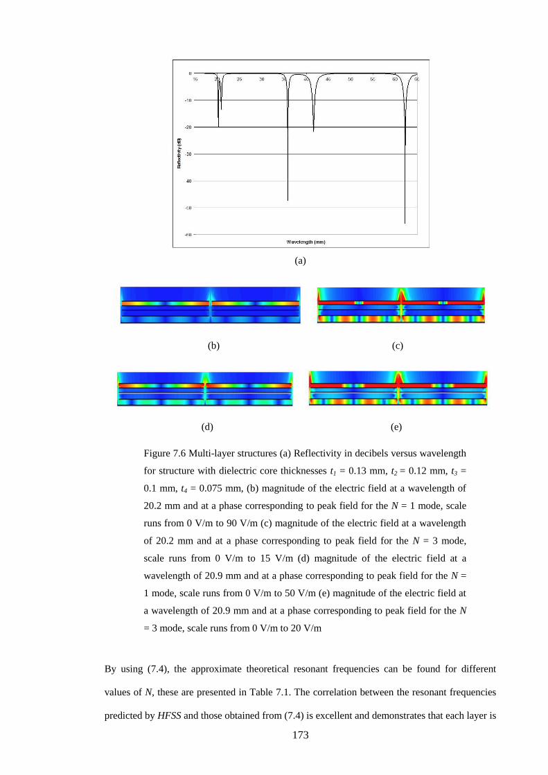
173
(a)
(b) (c)
(d) (e)
Figure 7.6 Multi-layer structures (a) Reflectivity in decibels versus wavelength
for structure with dielectric core thicknesses t1 = 0.13 mm, t2 = 0.12 mm, t3 =
0.1 mm, t4 = 0.075 mm, (b) magnitude of the electric field at a wavelength of
20.2 mm and at a phase corresponding to peak field for the N = 1 mode, scale
runs from 0 V/m to 90 V/m (c) magnitude of the electric field at a wavelength
of 20.2 mm and at a phase corresponding to peak field for the N = 3 mode,
scale runs from 0 V/m to 15 V/m (d) magnitude of the electric field at a
wavelength of 20.9 mm and at a phase corresponding to peak field for the N =
1 mode, scale runs from 0 V/m to 50 V/m (e) magnitude of the electric field at
a wavelength of 20.9 mm and at a phase corresponding to peak field for the N
= 3 mode, scale runs from 0 V/m to 20 V/m
By using (7.4), the approximate theoretical resonant frequencies can be found for different
values of N, these are presented in Table 7.1. The correlation between the resonant frequencies
predicted by HFSS and those obtained from (7.4) is excellent and demonstrates that each layer is

174
behaving as a largely independent resonator. Equation (7.4) also allows each of the resonances
in Figure 7.6(a) to be identified: the three longest-wavelength resonances are due to N = 1
modes in the alumina, FR4, and PET layers, the shortest-wavelength resonance, occurring at
20.2 mm is the N = 1 mode for the air layer. The mode at 20.9 mm is in fact the N = 3 mode in
the alumina layer which partially overlaps with the N = 1 air mode.
Alumina FR4 PET Air
N Eqn. (7.4) HFSS Eqn. (7.4) HFSS Eqn. (7.4) HFSS Eqn. (7.4) HFSS
1 61.3 62.3 40.8 41.6 35.8 35.8 20 20.2
2
3 20.4 20.9
Table 7.1 Resonant wavelengths in millimetres for Structure 4 – Multi-layer
structure as predicted using (7.4) and observed using HFSS
The identification of each mode using (7.4), can be corroborated by using HFSS to plot the
fields within the core: this is particularly useful for the closely-spaced N = 1 air and N = 3
alumina modes. Since these modes partially overlap, field plots at either wavelength (20.2 mm
or 20.9 mm) will show a resonance in both layers. However, the field strength exhibited by any
one mode will be a maximum at its centre resonant wavelength. Therefore, by plotting the
electric field and adjusting the phase to determine maximum field strength, it is possible to
determine which resonance on Figure 7.1(a) corresponds to which mode.
The instantaneous magnitude of the electric field within the dielectric layers of Structure 3 is
plotted in Figure 7.6(b) - (e). In Figure 7.6(b) and (c), both plotted at 20.2 mm wavelength, the
N = 3 and N = 1 modes are visible in the alumina and air layers respectively. The phase selected
in Figure 7.6(b) is that at which the N = 1 mode has its maximum field strength: approximately
90 V/m. In Figure 7.6(c) the phase selected is that at which the N = 3 mode has its maximum
strength: approximately 15 V/m.

175
By plotting the fields at 20.9 mm wavelength and adjusting phase, it can be seen that the peak
field of the N = 1 mode is approximately 60 V/m – much weaker than it was at 20.2 mm, see
Figure 7.6(d). Furthermore the peak field strength for the N = 3 mode is 20 V/m - higher than
was the case for 20.2 mm wavelength. This confirms that the 20.9 mm resonance in Figure
7.6(a) is due predominantly to the N = 3 mode in the alumina layer, whilst that at 20.2 mm is
predominantly due the N = 1 mode in the air layer.
The total absorption bandwidth afforded by this structure over the 15 mm to 70 mm wavelength
range is 65.4 dBmm which according to (7.3) is 95% of the theoretical limit, and is more than
double that of the optimised standard mono-grating. However, the reflectivity profile includes
the N = 3 resonance for alumina, the bandwidth of which should be excluded from the
summation for valid comparison to the standard mono-grating and to the narrowband limit (7.3)
which includes only the lowest order resonances. However, the partial overlap of the N = 1 air
and N = 3 alumina modes precludes this additional bandwidth being excluded from the
summation, and creates a small degree of ambiguity in the result that the structure achieves 95%
of the limit (7.3).
7.4.5 Structure 4 - Multiple permittivities
Structure 4 has a fixed period of 20 mm, each period containing two slits spaced apart by 10
mm and both having widths of 0.3 mm, the properties of the core material alternate between
adjacent cells. In the first cell the core material has a complex permittivity of εr1 =3.5 + i0.07 in
the second unit cell the complex permittivity is εr2 = 4.17 + i0.07, see Figure 7.1(g). The former
material is ficticous but might be achieved in practice by using a polymer, the latter material is
FR4 as per the previous chapters.

176
A series of structures spanning a range of core thicknesses was investigated. The reflectivity of
these structures as a function of wavelength is shown in Figure 7.7(a). Each structure supports
two resonances: one at approximately 41.5 mm and the other at approximately 38 mm
wavelength. From (7.4) it is clear that these correspond to the fundamental, N = 1 modes for the
cavities with permittivities εr1 =4.17 + i0.07 and εr1 =3.5 + i0.07 respectively.
(a)
(b)

177
(c)
Figure 7.7 Multiple-permittivity structure (a) Reflectivity in decibels versus
wavelength for structures with a range of dielectric core thicknesses (b)
Percent of narrowband bandwidth limit versus core thickness for the series of
multiple-permittivity structures (d) Reflectivity in decibels versus wavelength
as predicted by the finite element model for multiple-permittivity structures
with different values of loss tangent in the cavity with εr = 3.5
A core thickness of around 240 μm provides both greatest absorption depth and the also greatest
percentage of the theoretical limit (7.3) – see Figure 7.7(b). This structure achieves over 97% of
the narrowband limit (7.3) and therefore does constitute a small improvement over the standard
mono-grating but broadly equivalent performance to that of the other single-layer structures -
Structures 1 and 2.
Whilst a core thickness of 240 μm appears to provide optimum absorption bandwidth per unit
thickness, the depth of the shorter-wavelength resonance is only -8 dB, corresponding to 84% of
the incident radiation being absorbed. By contrast, the cavity in which εr = 4.17 absorbs over
99.9 % (-30 dB) of the incident radiation. Furthermore, the depth of the shorter-wavelength
resonance remained largely unaffected by alterations to the overall core thickness. This may be
due to the limited range of core thicknesses explored.
If the depth of both resonances could be simultaneously optimised then overall absorption
bandwidth might be increased. To this end the imaginary component of the core material in the
cavity with real permittivity equal to 3.5, was progressively decreased from 0.07 to 0.046, see

178
Figure 7.7(c). The depth of the shorter-wavelength resonance has increased from -8 dB to -12
dB whilst that of the longer-wavelength resonance has also increase from -40 dB to -50 dB.
However, the total absorption bandwidth has not changed significantly, remaining between 96%
and 98% of the limit (7.3).
By analogy with a series resonant circuit (Grant et al (1995) and Bowick (1982)), decreasing the
loss tangent within the cavity in which εr = 3.5, is the equivalent of decreasing the overall circuit
resistance. This decreased resistance results in an increase in the quality factor of the cavity: the
depth of the cavity may be increased but this is off-set by minor reductions to the width of the
resonance, rendering the overall bandwidth product largely unchanged.
7.5 Conclusions
This chapter has demonstrated that the standard mono-grating structure, when optimised by
altering core thickness, can achieve absorption bandwidths equivalent to approximately 93% of
the theoretical limit for narrowband absorbers. A series of optimised hybrid designs afford
greater absolute absorption bandwidth and allow the reflectivity profile to be tailored. However,
the hybrid designs are only a marginal improvement over the standard mono-grating in terms of
their bandwidth-to-thickness ratio.
Each of the structures investigated has its own advantages: the multilayer design, whilst thicker
than the others, is still grossly sub-wavelength and consequently of much lower profile than
conventional radar absorbers. It also offers the greatest opportunity to tailor the reflectivity
profile and ensure that absorption is produced at the desired frequency. Unlike some of the other
structures, its period is no greater than that of the standard mono-grating structure, meaning that
diffraction will be less of a problem. However, the overall bandwidth-to-thickness ratio for the
multi-layer design is likely to be slightly inhibited by the inclusion of numerous metal layers,
each of which contribute to the thickness of the structure but only absorb energy within a small
fraction of their thickness due to skin effects.

179
Consider that the skin depth of the copper at 10 GHz is approximately 0.6 μm (Grant et al
(1995)), therefore only the outer 0.6 μm of the copper will absorb energy and contribute to the
overall absorption bandwidth: the volume of metal more than 0.6 μm from the surface of the
metal will not contribute to absorption but will contribute to the overall thickness of the
structure and is hence superfluous. In Structure 3 the copper layers are each 18 μm thick hence,
allowing for absorption in the outer 0.6 μm of the copper means that almost 90% of the copper
volume is not absorbing any significant amount of energy.
Both the multiple permittivity (Structure 4) and multiple discrete period (Structure 1) structures
offer two resonances from a single-layer. However, both structures have a period significantly
longer than the standard mono-grating and will begin to diffract at longer wavelengths than
would otherwise be the case. The multiple-period structure is significantly easier to fabricate
than the multiple-permittivity structure, but the latter might prove easier to optimise. Both
structures have just one metal layer that contributes to overall thickness for bandwidth limit
calculations: hence they are able to achieve a higher percentage of the theoretical limit than the
multi-layer structure.
The multiple continuous period structure (Structure 2) affords several closely-spaced absorption
bands and affords the same bandwidth per unit thickness Structures 1 and 4. However, as a
consequence of the non-parallel slits, the frequencies at which the modes are excited are not
readily predictable which is a significant obstacle to tailoring the reflectivity profile.
In summary, this chapter constitutes efforts to increase the absorption bandwidth of the
microcavity array structures. The results demonstrate that the existing bandwidth-to-thickness
theories cannot be bypassed and that when attempts are made to increase the bandwidth, the
response of the structure changes in such as way as to the limit set by the bandwidth theories
and that these limits cannot be exceeded or violated in any way. The primary advantage of the
structures studied herein is that they permit the bandwidth to be re-distributed as required rather
than increasing the total bandwidth product.

180
Chapter 8
Conclusions
8.1 Summary of thesis
The work presented in this thesis has demonstrated that contrary to conventional thinking, ultra-
thin structures can exhibit highly efficient absorption of microwaves despite being more than
two orders of magnitude thinner than the operating wavelength. This creates the possibility of
designing low profile, lightweight and even flexible materials and claddings which can help
ensure a much higher degree of control over radio frequency signals across a vast range of
applications. Furthermore, frequency-selective transmission can also be mediated by variants of
the absorber structure thus affording precise control over the radio frequency environment.
The work detailed in Chapter 4 reveals that the ultra-thin cavity structures support a series of
pseudo-Fabry-Perot resonant modes, the frequencies of which are determined by the inter-slit
distance and the refractive index of the dielectric material filling the core. By considering the
momentum of the incident photons, the resonant frequencies of these modes under azimuthal
and polar incident angle variation has been accurately predicted. Further experimental work has
demonstrated that these mono-grating structures are highly efficient at converting one
polarisation state into the other with up to 50% of the incident field being re-emitted in the
opposing polarisation state.
Finite element modelling has elucidated the mechanism which underpins the frequency-
selective absorption, and has revealed that the resonance depth can be optimised by adjusting
the steady state amplitude of the resonant mode; this in turn is altered by changes to the
geometry and material properties of the structure. The modelling work also allows the form of
the resonant modes excited to be determined. This leads to the startling and counterintuitive
discovery that the modes undergo ―phrase compression,‖ being forced to undergo a phase
change of half a wavelength in a distance several orders of magnitude smaller than the
wavelength.

181
Further work considered the use of the ultra thin cavities as frequency-selective filters of
microwave radiation. Again it was found that the nature of the mode and in particular the phase
compression within the sub-wavelength apertures is key to determining the resonant frequencies
of the structures.
Chapter 5 focused on two-dimensional ―bi-grating,‖ structures in which two orthogonal sets of
sub-wavelength apertures have been formed in the upper conducting layer. These structures
support more modes than their mono-grating equivalents due to the greater number of scattering
vectors that are accessible. They also exhibit a remarkably high level of azimuth and incident
angle independence with the fundamental appearing completely invariant for both polarisation
states. Furthermore, the bi-grating structures exhibit very little polarisation conversion, in
contrast to the mono-grating equivalent. Again the resonant frequencies of the modes are
accurately predicted by considering the momentum of the incident photons. The finite element
model is used to explore the character of the modes and reveals that both degenerate and
coupled modes are supported, the former resulting from simultaneous scattering from
orthogonal lattice vectors and the latter from lattice vectors indigenous to two-dimensional
gratings.
Chapter 6 details the investigation of two hexagonally symmetric ―tri-grating,‖ structures each
of which features three sets of sub-wavelength apertures each rotated by 60° relative to the other
two. On the first sample all three sets of slits intersect at common points creating an array of
equilateral triangles. In the second structure each set of grooves is off-set by half its repeat
period relative to the other two sets, hence all points of intersection feature slits from only two
of the three sets and a pattern of hexagons interspersed with equilateral triangles is formed.
Comparison of their relative responses demonstrates that it is the repeat period of the slits and
their orientation, rather than the shape of the metal patches that determines the behaviour.
Furthermore, both structures exhibit reflectivity spectra which are incident and azimuthal angle
independent for any polarisation state and contain more resonances than the bi-grating
equivalent.

182
Chapter 7 considered the absorption bandwidth of the ultra thin cavities and presented four
strategies for maximising this bandwidth by exciting multiple resonant mode series through a
multiplicity of cavity lengths and refractive indices. The specific embodiments included a
structure which alternated between two inter-slit distances and hence supported two
―fundamental,‖ resonances. Similarly a structure in which the permittivity of the dielectric core
alternated between adjacent unit cells supported two fundamental modes. Other approaches
included non-parallel slits and multi-layers structures. All these approaches proved successful in
increasing the total absorption bandwidth versus that of the simple mono-grating structure.
However, in all cases the total bandwidth was fundamentally limited by the thickness of the
structures and their magnetic permeability as expected on the basis of established theory.
8.2 Ideas for future work
The work embodied in this thesis has considered the performance of ultra thin cavity structures
as devices for the control and manipulation of microwave radiation. In addition to having many
applications, the range of possible geometries and configurations of these cavities is myriad and
hence constitutes a massive body of potential future work, the scope of which is limited only by
imagination. Presented here is a small sample of the possible interpretations of and extensions to
the work presented herein.
One could also envisage further single layer transmission structures in which the array of slits in
the upper metal layers was accompanied by a solitary slit in the lower layer. The number of slits
in the lower layer could be progressively increased and transmission efficiency as a function of
the number of slits investigated. In fact, basic tests on hand-made samples of this type were
conducted using the focused horn apparatus. The results indicated an increase in transmission
efficiency with number of slits. However, due to the hand-made nature of the samples these
results were not included: further testing with more precise sample formed by etching would
provide more reliable data.

183
(a)
(b)
(c)
Figure 8.1 Hybrid transmission structures
(a) array of slits in the upper metal layer, single slit in the lower metal layer (b)
rotation of slits in lower metal layer relative to those in the upper metal layer,
layers shown separately (c) progressive reduction in slit number to concentrate
field
One might also pursue the effect of rotating the slits in the lower metal layer relative to those in
the upper metal layer hence introducing a degree of chirality and raising the possibility of
polarisation conversion via transmission. This approach creates a periodic structure of longer
period – the period is dictated by the angle of rotation. to create a working device may require
adiabatic rotation: only small twist angles. It might also be possible to create extremely high
field concentrations by combining the multi-layer and single slit ideas. Consider an aligned
transmission sample as per those in Chapter 4, wherein the number of slits could be

184
progressively reduced layer after layer. This might have the effect of channelling the energy
collected by many slits towards a single exit slit.
Multi-layer absorbing structures were shown in Chapter 8, to exhibit increased absorption
bandwidth. It might be feasible to create a pseudo-fractal structure similar to the multi-layer
geometry but in which the period changes by a factor between layers – see Figure 8.2. However,
this may only work if the radiation can progress through the upper layer to the lower layer,
which in turn may require the periods of the lower cavities to be multiples of the upper cavities.
This could combine in one device the ability to manipulate radiation from disparate regions of
the electromagnetic spectrum such as the microwave region investigated by this work and the
optical region investigated by other including Hibbins et al (2006).
Figure 8.2 Pseudo-fractal multi-layer absorbing structure
In addition to altering the physical geometry of the structures, the material properties of both the
conducting and dielectric layers could be considered. Introducing magnetic material to the core
would serve to increase absorption bandwidth in accordance with established theory, Brewitt-
Taylor (1999) and Rozanov (2000), whilst the use of dielectrics which are active rather than
passive would create devices whose bandwidth is not limited by the aforementioned theoretical
results. The addition of liquid crystal material to the core might permit dynamic control over the
microwave reflectivity and transmissivity of the structures if a method could be found for
applying a voltage across the core and hence polarising the material. One might also investigate
the effect of adding two media of differing refractive index to same cavity – see Figure 8.3.
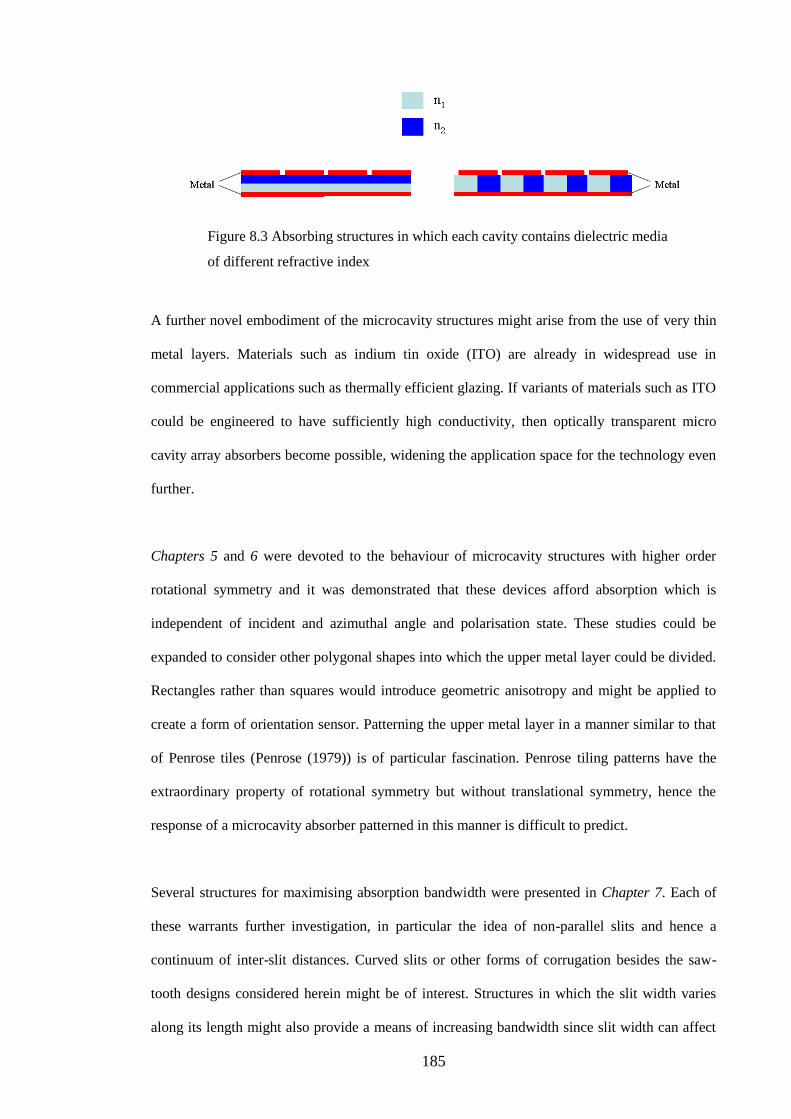
185
Figure 8.3 Absorbing structures in which each cavity contains dielectric media
of different refractive index
A further novel embodiment of the microcavity structures might arise from the use of very thin
metal layers. Materials such as indium tin oxide (ITO) are already in widespread use in
commercial applications such as thermally efficient glazing. If variants of materials such as ITO
could be engineered to have sufficiently high conductivity, then optically transparent micro
cavity array absorbers become possible, widening the application space for the technology even
further.
Chapters 5 and 6 were devoted to the behaviour of microcavity structures with higher order
rotational symmetry and it was demonstrated that these devices afford absorption which is
independent of incident and azimuthal angle and polarisation state. These studies could be
expanded to consider other polygonal shapes into which the upper metal layer could be divided.
Rectangles rather than squares would introduce geometric anisotropy and might be applied to
create a form of orientation sensor. Patterning the upper metal layer in a manner similar to that
of Penrose tiles (Penrose (1979)) is of particular fascination. Penrose tiling patterns have the
extraordinary property of rotational symmetry but without translational symmetry, hence the
response of a microcavity absorber patterned in this manner is difficult to predict.
Several structures for maximising absorption bandwidth were presented in Chapter 7. Each of
these warrants further investigation, in particular the idea of non-parallel slits and hence a
continuum of inter-slit distances. Curved slits or other forms of corrugation besides the saw-
tooth designs considered herein might be of interest. Structures in which the slit width varies
along its length might also provide a means of increasing bandwidth since slit width can affect

186
resonant frequency as shown in Chapter 4. As outlined above, changing the core material
properties could create structures which are not bound by the same bandwidth-to-thickness ratio
as those studied in Chapter 8 and could exhibit hitherto unachieved bandwidths.
One very important conclusion that can be drawn from the work presented herein, is that
viewing the microcavity structures as pseudo Fabry-Perot resonators is too simple a description.
This description is useful only for an estimate of the resonant frequency of the simple mono-
grating structure at normal incidence. Changes to incident angle, polarisation state and
azimuthal angle all serve to alter the resonant frequency for the reasons detailed in Chapter 4.
Furthermore, geometric factors such as slit width, core thickness and the shape of the polygons
into which the upper metal layer is divided, all influence the frequencies of the resonant modes
supported. A further piece of work could be undertaken to establish a firmer theoretical basis for
the dependence of resonant frequencies on these factors.
8.3 List of publications
Squeezing millimetre waves into microns
Alastair P. Hibbins, J.R. Sambles, C.R. Lawrence and J.R. Brown
Physical Review Letters, 92, 143904 (2004)
Angle independent microwave absorption by ultra thin microcavity arrays
J.R. Brown, Matthew J. Lockyear, Alastair P. Hibbins, C.R. Lawrence and J.R. Sambles
Journal of Applied Physics 104, 043105 (2008)
Angle independent resonant absorption of microwave radiation by hexagonally symmetric ultra
thin microcavity arrays
J.R. Brown, Matthew J. Lockyear, Alastair P. Hibbins, C.R. Lawrence and J.R. Sambles
Submitted for publication to J. Phys. D. Applied physics

187
Ultra thin microcavity arrays for optimum absorption bandwidth
J.R. Brown, Alastair P. Hibbins, C.R. Lawrence and J.R. Sambles
Awaiting clearance for publication

188
References
Ashcroft, N. (1976) Solid State Physics, Holt, Rinehart
and Winston, New York
Bode, H.W. (1945) Network analysis and
feedback amplifier design, Van
Norstrand, New York
Bowick, C. (1982) RF Circuit Design, 1st ed.
(Newnes, MA, USA) Chap. 2
Brewitt-Taylor, C.R. (2008) NATO Adv. Res. Wkshop, Meta.
2008, Marakesh
Brewitt-Taylor, C.R. (2007) IET Microwav. Antennas
Propag., 2007, 1, pp. 255 - 260
Brewitt-Taylor, C.R., (1999) Antennas & Propagation
Society International
Symposium, Vol.3, p1938-
1941.
Broas, R. F. J., Sievenpiper, D, (2005) IEEE Trans. Antennas and
and Yablonovitch, E. Propagat. 2005, 53, 1377–1381
Broas, R. F. J., Sievenpiper, D., (2001) IEEE Trans. Micro. Theory and
and Yablonovitch, E. Techn. 2001, 49, 1262–1265
Brown, J. R., Lawrence, C. R., (2008) Patent application:
and Damerell, W. N. WO/2008/075039,
PCT/GB2007/004877
Brown, J. R., Hibbins, A. P., Lockyear, (2008) Journal of Applied Physics,
M. J., Lawrence, C. R., and Sambles, J. R. 104, 043105 1-6
Bryan-Brown, G.P. and Sambles, J.R. (1990) J. Mod. Opt., 37, 1227
Butterworth, K.S., Sowerby, K.W. (1997) Proc. 47th IEEE Vehicular and
Williamson, A.G. Technology Conference 1420
– 1424
Chandran, A. R., Matthew, T., (2003) Inc. Microwave Opt. Technol.
Aanandan, T. K., Mohanan, P. Lett., 40, 246-248
and Vasudevan, K.,
Chandran, A. R., Matthew, T., (2004) Electronics Letters, 40, 1245–
Aanandan, T. K., Mohanan, P., 1246
and Vasudevan, K.,
Collin, R.E. (1991) Field theory of guided waves,
IEEE New York, 2nd
edition
Conolly, T. M. and Luoma, E. J. (1977) US Patent No. 4, 038, 660
Ebbesen, T.W., Lezec, J. J., Ghaemi, H. F., (1998) Nature (London), 391, 667
Thio, T. and Wolfe, P. A.,

189
Eurotech Group plc. (1998) Exmouth, UK.
R.M. Fano (1950) J. Franklin Inst., vol.249,
no. 1 – 2, pp. 57- 83, 139 –
154
Gao, Q., Yan, D. -B., Yan, N. -C., (2005) IEE Electronics letters 41,
and Yin, Y. 936
Grant, I. S. and Phillips, W. R., (1995) Electromagnetism, 2nd
ed.
John Wiley & Sons,
Chichester, Chap. 12.
S.H. Hall and H.L. Heck (2009) Advanced Signal Integrity for
High Speed Digital Design,
John Wiley & Sons Inc.
Hoboken, New Jersey,
Chapter 6
Hallam, B.T., Lawrence, C.R., (2004) Appl. Phys. Lett. 84, 849
Hooper, I.R. and Sambles, J.R.,
Hibbins, A. P., Murray, W. A., Tyler, J., (2006) Phy. Rev. B, 74, 073408 1–4
Wedge, S., Barnes, W. L. and Sambles, J. R.
Hibbins, A.P., Sambles, J.R., (2004) Phys. Rev. Lett. 92, 143904
Lawrence, C.R. and Brown, J.R.
High Frequency Structure Simulator, (1984 - 2009) Ansys Corporation,
Versions 8 – 11 Pitsburgh, PS, USA
Houliston, B., Parry, D., (2009) N Z Med. J. 122 (1297) 9 –
Webster, C. S., and Merry, A.F. 16
EPC Global (2010) http://www.epcglobalinc.org
Sarbanes-Oxley (2002) http://www.soxlaw.com/
Hecht, E. (1998) Optics, Addison Wesley
Longman, Inc. USA, Chapters
4 and 10
Huebner, K.H., (2001) The finite element method
for Engineers, John Wiley
& Sons, Inc. Chapter 1.
James, J.F., and Steinberg, R.S. (1969) The Design of optical
spectrometers, Chapman
and Hall, London
Knott, E. F., Schaeffer, J. F., (1993) Radar Cross Section, 2nd
ed.
and Tuley, M. T. Artech House, Inc,
Norwood, USA, Chap. 8

190
L. H. Hemming (2002) Electromagnetic anechoic
chambers, Wiley IEEE press
Lockyear, M. J. Hibbins, A. P., (2005) Applied Physics Letters,
Sambles, J. R., and Lawrence C. R. 2005, 86, 184109 1–3,
Lockyear, M. J., Hibbins A. P., (2009) Phys. Rev. Lett. 102,
and Sambles J. R. 073901
Lockyear, M. J., Hibbins A. P., (2003) Appl. Phys. Lett. Vol. 83.
and Sambles, J. R. No. 4
Lockyear, M. J., Hibbins, A. P., (2009) Appl. Phys. Lett. 94,
Sambles, J. R., Hobson, P.A., 041913
and C.R. Lawrence
Lockyear, M. J., Hibbins, A.P., (2004) Applied Physics Letters,
Sambles, J.R. and Lawrence, C.R. 84, 2040
Munk, B.A. (2000) Frequency selective
surfaces, theory and
design, Wiley, New York
Navarro-Cia, M., Beruete, M. Agrafiotis, (2009) Optics Express, 18184,
S., Falone, F., Sorolla, M. and Maier, S. A. Vol. 17. No. 20
Nicholson, A.M. and Ross, G.F. (1970) IEEE Trans. Instrum.
Meas. Vol. IM-19 pp. 337-
382
Pendry, J.B., Martin-Moreno, L., (2004) Science, 305, pp.847 – 848
and Garcia-Vidal, F.J.
Penrose, R. (1979) Patent application
GB1548164 (A)
Qian, Y., Sievenpiper, D. Radisic, V., (1998) IEEE RAWCON
Yablonovitch, E. and T. Itoh, proceedings, pp. 221 - 4
Raether, H. (1988) Surface Plasmons on
smooth and rough surfaces
and on gratings, Berlin,
Springer
RFID Journal (2003) http://www.rfidjournal.com/
article/articleview/539/1/1/
Rozanov, K.N. (2000) IEEE Trans. Antennas
Propag., 48, (8), pp.1230 –
1234

191
Ruck, G. T. (1970) Radar cross section
handbook, Plenum press,
New York, Chapter 8.
Rudin, W. (1976) Principles of Mathematical
Analysis, McGrawHill,
New York
Salisbury, W.W. (1952) US Patent No. 2,599,944
Sarychev, A.K., Shvets, G. and (2006) Phys. Rev. E, 73, 036609, 1 -
V.M. Shalaev 10
Sievenpiper, D. F., Schaffner, J. H., Song, (2003) IEEE Trans. Antennas,
H. J., Loo, R. Y. and Tangonan, G. Propag. 51, 2713.
Sievenpiper, D., Zhang, L. (1999) IEEE MTT-S Digest
and Yablonovitch, E.
Sievenpiper, D., Zhang, L. J., Broas, R. F. J., (1999) IEEE Trans. Microwave
Alexpolous, N. G., and Yablonovitch, E. Theory Tech.47, 2059.
Suckling, J. R., Sambles, J. R., (2007) New Journal of Physics,
and Lawrence, C. R. 9, 1 – 11
Suckling, J.R., Hibbins, A.P, Lockyear. M.J., (2004) Phys. Rev. Lett. 92,
Preist, T.W., Lawrence, C.R. and Sambles, J.R. 147401
Takakura, Y. (2001) Phys. Rev. Lett., 86,
5601–5603
Tennant, A. and Chambers, B. (2004) Smart Mater. Struct. 13,
122.
Tennant, A., and Chambers, B. (2004) IEEE Microw. Wirel.
Compon. Lett. 14, 46.
Tennant, A., Chambers, B. (2006) Smart Mater. Struct. 15
468 – 472
Watson-Watt, R. A. (1935) GB patent GB593017
Weir, W.B. (1974) Proc. IEEE, vol. 62, pp.
33-36
Yang, S-H, and Bandaru, P.R. (2008) Optical Engineering
47(2), 029001
Zhang, Y., von Hagen, J., Younis, (2003) IEEE Trans. Antennas
M., Fischer, C. and Wiesbeck, W. Propag. 51, 2704

192
Zienkiewicz, O.C., Taylor, R.L. and Zhu, J.Z. (2005) The finite element
method: its basis and
fundamentals, 6th
edition, Elsevier
Butterworth-Heineman,
Burlington, MA, USA,