the little box challenge ultra-compact gan- or sic-based ... · ultra-compact gan- or sic-based ....
TRANSCRIPT

Johann W. Kolar
Swiss Federal Institute of Technology (ETH) Zurich Power Electronic Systems Laboratory
www.pes.ee.ethz.ch
Ultra-Compact GaN- or SiC-Based Single-Phase DC/AC Power Conversion
The Little Box Challenge

DC-AC Converter
D. Bortis
Power Electronic Systems Laboratory
Johann W. Kolar
AC-DC Converter
M. Leibl
D. Neumayr D. Rothmund
J. Schäfer L. Schrittwieser
DC-DC Converter
P. Bezerra
Industry Relations R. Coccia / B. Seiler
AC-AC Converter
J. Azurza J. Böhler P. Czyz
Th. Guillod
Multi-Domain Modeling
Advanced Mechatronics
M. Antivachis M. Flankl
M. Mauerer S. Miric
Secretariat M. Kohn / Y. Schnyder
Administration P. Albrecht / P. Maurantonio
Computer Systems C. Stucki
Electronics Laboratory P. Seitz
O. Knecht
22 Ph.D. Students 2 Post Docs
ETH Zurich - Power Electronic Systems Laboratory
Leading Univ. in Europe
F. Krismer
Magnetic Levitation
Wireless Power
Th. Holenstein
P. Püntener M. Schuck
T. Wellerdieck
Ch. Gammeter M. Guacci
P. Papamanolis

D. Bortis D. Neumayr
0. Knecht F. Krismer M. Guacci
L. Camurca M. Kasper
Acknowledgement E. Hatipoglu
1/68
Outline
The Little Box Challenge Little Box 1.0 Concepts & Performances of Other Finalists Little Box 2.0
Conclusions

Requirements The Grand Prize Finalists & Finals
Little Box Challenge

Design / Build the 2kW 1-ΦSolar Inverter with the Highest Power Density in the World Power Density > 3kW/dm3 (> 50W/in3, multiply kW/dm3 by Factor 16) Efficiency > 95% Case Temp. < 60°C EMI FCC Part 15 B
Push the Forefront of New Technologies in R&D of High Power Density Inverters
!
!
!
!
2/68

The Grand Prize
Timeline – Challenge Announced in Summer 2014 – 2000+ Teams Registered Worldwide – 100+ Teams Submitted a Technical Description until July 22, 2015 – 18 Finalists (3 No-Shows)
$1,000,000
Highest Power Density (> 50W/in3) Highest Level of Innovation
3/68

4/68
Finalists
- 5 Companies - 6 Consultants - 4 Universities
* and FH IZM / Fraza d.o.o.
Univ. of Tennessee
Univ. of Illinois
Virginia Tech Rompower
Schneider Electric
Tommasi Bailly
CE+T
Energy Layer
AHED OKE Services
Cambridge Active Magnetics
AMR
Venderbosch
Fraunhofer IISB
*
15 Teams/Participants in the Final @ NREL

– Finalists Invited to NREL / USA – Presentations on Oct. 21, 2015 – Subsequent Testing by NREL
5/68
Final Presentations

Acknowledgement
Little Box 1.0
Converter Topology Modulation & Control Technologies /Components Mechanical Concept Exp. Analysis

Derivation of Converter Concept

1-Φ Output Power Pulsation Buffer

Parallel Buffer @ DC Input
Series Buffer @ DC Input
Parallel Approach for Limiting Voltage Stress on Converter Stage Semiconductors
Power Pulsation Buffer
6/68

Passive Power Pulsation Buffer (1)
C > 2.2mF / 166 cm3 Consumes 1/4 of Allowed Total Volume !
S0 = 2.0 kVA cos Φ0 = 0.7 VC,max = 450 V ΔVC/VC,max=3 %
Electrolytic Capacitor
5 x 493μF/450 V C = 2.46 mF
7/68
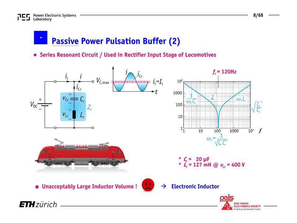
* Cr = 20 μF * Lr = 127 mH @ vLr = 400 V
Series Resonant Circuit / Used in Rectifier Input Stage of Locomotives
Unacceptably Large Inductor Volume ! Electronic Inductor
fr = 120Hz
Passive Power Pulsation Buffer (2)
8/68
f

Coupling Capacitor & “Electronic Inductor” Processing Only Partial Power
Low UC,aux Low Converter Losses High Values of CK, Caux Required for Low UC,aux Full-Bridge Aux. Converter Allows Lower UC,aux
Partial Active Power Pulsation Buffer
* Ertl (1999) * Enslin (1991) * Pilawa (2015)
Electronic Inductor
9/68
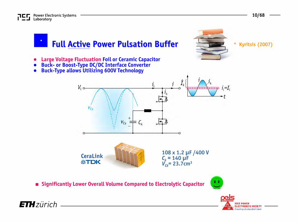
Large Voltage Fluctuation Foil or Ceramic Capacitor Buck- or Boost-Type DC/DC Interface Converter Buck-Type allows Utilizing 600V Technology
Significantly Lower Overall Volume Compared to Electrolytic Capacitor
108 x 1.2 μF /400 V Ck ≈ 140 μF VCk= 23.7cm3
CeraLink
Full Active Power Pulsation Buffer * Kyritsis (2007)
10/68

Output Stage Topology / Modulation

– Boost-Type 1-Φ PFC Rectifier
– DC/|AC| Buck Converter & Mains Frequency “Unfolder”
Analysis Only for cos Φ = -1
Inversion of Basic 1-Φ PFC Rectifier Topology
Derivation of Output Stage Topology (1)
* Erickson (2009)
11/68
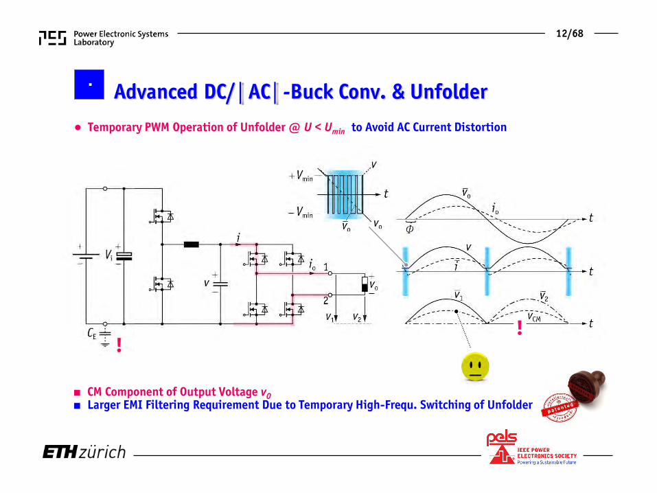
CM Component of Output Voltage vO Larger EMI Filtering Requirement Due to Temporary High-Frequ. Switching of Unfolder
Temporary PWM Operation of Unfolder @ U < Umin to Avoid AC Current Distortion
! !
Advanced DC/AC-Buck Conv. & Unfolder
12/68
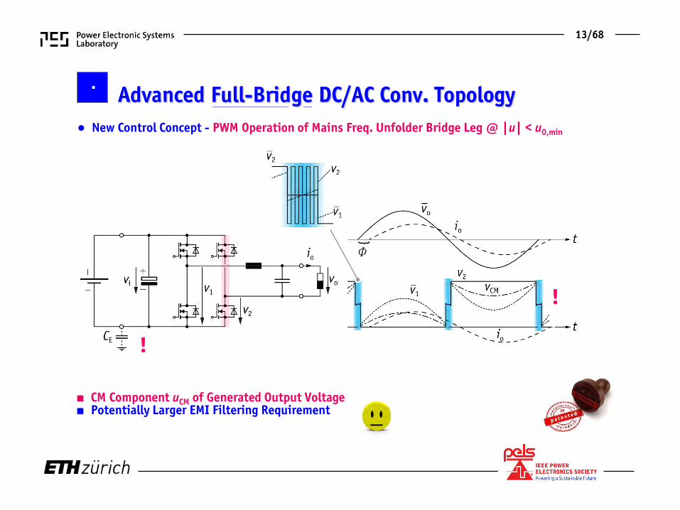
New Control Concept - PWM Operation of Mains Freq. Unfolder Bridge Leg @ |u| < u0,min
CM Component uCM of Generated Output Voltage Potentially Larger EMI Filtering Requirement
!
!
Advanced Full-Bridge DC/AC Conv. Topology
13/68

Symmetric PWM Operation of Both Bridge Legs No Low-Frequency CM Output Voltage Component
DM Component of u1 and u2 Defines Output uO CM Component of u1 and u2 Represents Degree of Freedom of the Modulation (!)
Symmetric PWM Full-Bridge AC/DC Conv. Topology
14/68
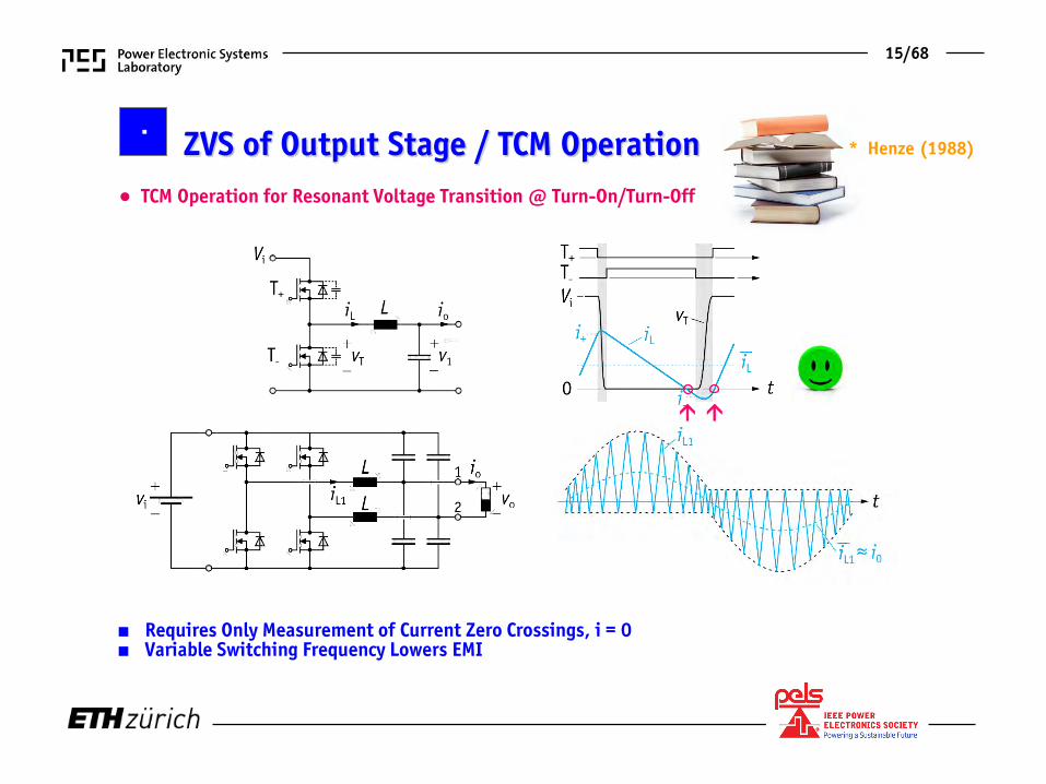
Requires Only Measurement of Current Zero Crossings, i = 0 Variable Switching Frequency Lowers EMI
TCM Operation for Resonant Voltage Transition @ Turn-On/Turn-Off
ZVS of Output Stage / TCM Operation
* Henze (1988)
15/68

4D-Interleaving Interleaving of 2 Bridge Legs per Phase - Volume / Filtering / Efficiency Optimum Interleaving in Space & Time – Within Output Period Alternate Operation of Bridge Legs @ Low Power Overlapping Operation @ High Power
Opt. Trade-Off of Conduction & Switching Losses / Opt. Distribution of Losses
16/68

Remark: i TCM Inverter Topology
* P. Jain (2015)
TCM : Challenging Inductor Design Superposition of HF & LF Currents iTCM: Adding LC-Circuit between Bridge Legs Separation of LF & HF Currents L >>LB
Low Output Current Ripple Reduced Filtering Effort PWM Modulation Applicable Simple Control Strategy Dedicated LF and HF Inductor Designs Possible Improved Converter Efficiency
– TCM – iTCM
17/68
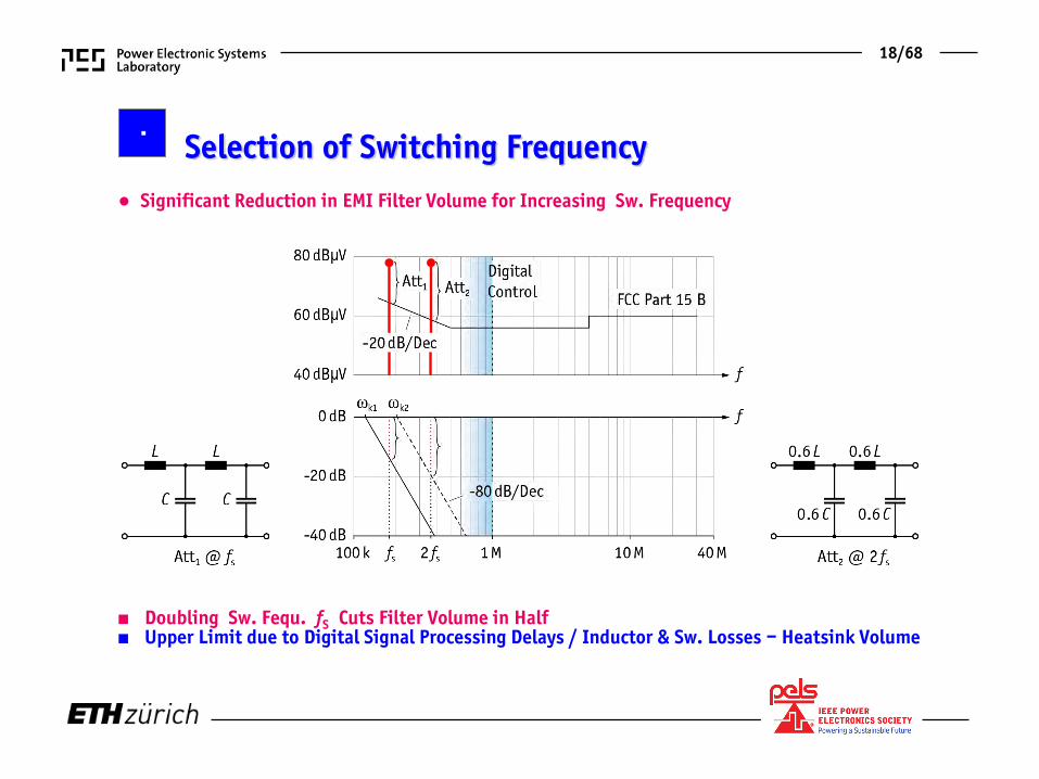
Selection of Switching Frequency Significant Reduction in EMI Filter Volume for Increasing Sw. Frequency
Doubling Sw. Fequ. fS Cuts Filter Volume in Half Upper Limit due to Digital Signal Processing Delays / Inductor & Sw. Losses – Heatsink Volume
18/68

EMI Filter Topology (1) Conventional Filter Structure – DM Filtering Between the Phases – CM Filtering Between Phases and PE
CM Cap. Limited by Earth Current Limit – Typ. 3.5mA for PFC Rectifiers (GLBC: 5mA then 50mA !) Large CM Inductor Needed – Filter Volume Mainly Defined by CM Inductors
19/68

EMI Filter Topology (2) Filter Structure with Internal CM Capacitor Feedback Filtering to DC- (and optional to DC+)
No Limitation of CM Capacitor C1 Due to Earth Current Limit µF Instead of nF Can be Employed Allows Downsizing of CM Inductor and/or Total Filter Volume
20/68

Final Converter Topology
ZVS of All Bridge Legs @ Turn-On/Turn-Off in Whole Operating Range (4D-TCM-Interleaving) Heatsinks Connected to DC Bus / Shield to Prevent Cap. Coupling to Grounded Enclosure
Interleaving of 2 Bridge Legs per Phase Active DC-Side Buck-Type Power Pulsation Buffer 2-Stage EMI AC Output Filter (1) Heat Sink
(2) EMI Filter (3) Power Pulsation Buffer (4) Enclosure
21/68
S

Power Semiconductors HF Inductors
Cooling Etc.
Technologies

Accurate Measurement of ZVS Losses Using Calorimetric Approach High Sw. Frequency for Large Ratio of Sw. and Conduction Losses
Evaluation of Power Semiconductors (1)
22/68
Direct Measurement of the Sum of Sw. and Conduction Losses Subtraction of the Conduction Losses Known from Calibration Fast Measurement by Cth.ΔT/Δt Evaluation

Evaluation of Power Semiconductors (2)
Comparison of Soft-Switching Performance of ~60mΩ, 600V/650V/900V GaN, SiC, Si MOSFETs Measurement of Energy Loss per Switch and Switching Period
GaN MOSFETs Feature Highest Soft-Switching Performance Similar Soft-Switching Performance Achieved with Si and SiC Almost No Voltage-Dependency of Soft-Switching Losses for Si-MOSFET
23/68
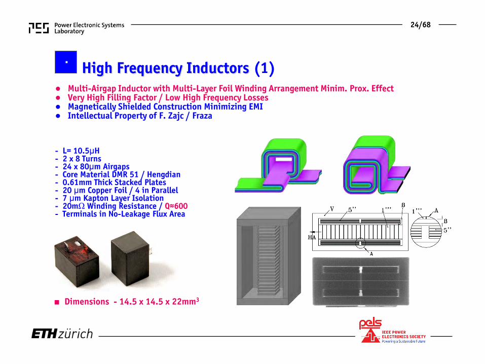
High Frequency Inductors (1)
Dimensions - 14.5 x 14.5 x 22mm3
- L= 10.5μH - 2 x 8 Turns - 24 x 80μm Airgaps - Core Material DMR 51 / Hengdian - 0.61mm Thick Stacked Plates - 20 μm Copper Foil / 4 in Parallel - 7 μm Kapton Layer Isolation - 20mΩ Winding Resistance / Q≈600 - Terminals in No-Leakage Flux Area
Multi-Airgap Inductor with Multi-Layer Foil Winding Arrangement Minim. Prox. Effect Very High Filling Factor / Low High Frequency Losses Magnetically Shielded Construction Minimizing EMI Intellectual Property of F. Zajc / Fraza
24/68

High Frequency Inductors (2) High Resonance Frequency Inductive Behavior up to High Frequencies Extremely Low AC-Resistance Low Conduction Losses up to High Frequencies High Quality Factor
25/68
Shielding Eliminates HF Current through the Ferrite Avoids High Core Losses Shielding Increases the Parasitic Capacitance

Comparison of Temp. Increase of a Bulk and a Sliced Sample @ 70mT / 800kHz
Cutting of Ferrite Introduces Mech. Stress Significant Increase of the Loss Factor Reduction by Polishing / Etching (5 μm)
x 7 (!)
* Knowles (1975!)
High Frequency Inductors (3)
26/68

Thermal Management
Evaluation of Optimum Heatsink Temperature for Thermal Isolation of Converter
30°C max. Ambient Temperature 60°C max. Allowed Surface and Air Outlet Temperature
Minimum Volume Achieved w/o Thermal Isolation with Heatsink @ max. Allowed Surface Temp.
27/68

Thermal Management Overall Cooling Performance Defined by Selected Fan Type and Heatsink
– Axial Fan – Radial Blower
– Square Cross Section
of Heatsink for Using a Fan
– Flat and Wide
Heatsink for Blower
28/68
Optimal Fan and Heat Sink Configuration Defined by Total Cooling System Length Cooling Concept with Blower Selected Higher CSPI for Larger Mounting Surface

30mm Blowers with Axial Air Intake / Radial Outlet Full Optimization of the Heatsink Parameters
- 200um Fin Thickness - 500um Fin Spacing - 3mm Fin Height - 10mm Fin Length - CSPI = 37 W/(dm3.K) - 1.5mm Baseplate
CSPIeff= 25 W/(dm3.K) Considering Heat Distribution Elements Two-Side Cooling Heatsink Temperature = 52°C @ 80W (8W by Natural Convection)
Final Thermal Management Concept (1)
29/68
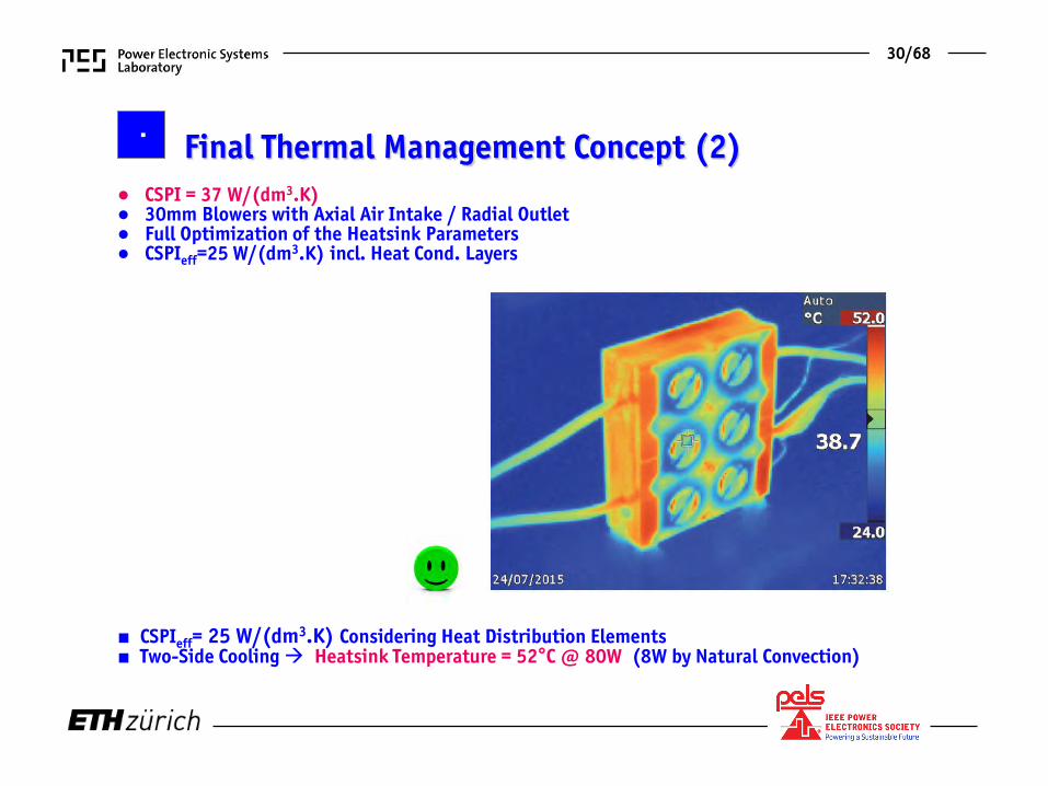
CSPI = 37 W/(dm3.K) 30mm Blowers with Axial Air Intake / Radial Outlet Full Optimization of the Heatsink Parameters CSPIeff=25 W/(dm3.K) incl. Heat Cond. Layers
CSPIeff= 25 W/(dm3.K) Considering Heat Distribution Elements Two-Side Cooling Heatsink Temperature = 52°C @ 80W (8W by Natural Convection)
Final Thermal Management Concept (2)
30/68

i = 0 Detection
Analyzed Methods • Shunt Current Measurement • Measurement of the Rds,on • Two Antiparallel Diodes • Giant Magneto-Resistive Sensor • Hall Element • Saturable Inductor
Losses, No Galvanic Isolation, Low Signal-to-Noise Ratio (SNR), Size, Bandwidth, Realization Effort
Various Drawbacks
Galvanic Isolation, High SNR, Small Size, High Bandwidth, Simple Design Min. Core Volume/Cross Section for Min. Core Losses
31/68

Saturable Inductor – Toroidal Core R4 x 2.4 x 1.6, EPCOS (4mm Diameter) – Core Material N30, EPCOS
Operation Tested up to 2.5MHz Switching Frequency
32/68
i = 0 Detection

Active Power Pulsation Buffer New Cascaded Control Structure
P-Type Resonant Controller Feedforward of Output Power Fluctuation Underlying Input Current (ii) / DC Link Voltage (uC) Control
33/68

Final Active Power Pulsation Buffer High Energy Density 2nd Gen. 400VDC CeraLink Capacitors Utilized as Energy Storage Highly Non-Linear Behavior Optimal DC Bias Voltage of 280VDC Losses of 6W @ 2kVA Output Power
Effective Large Signal Capacitance of C ≈160μF
- 108 x 1.2μF /400 V - 23.7cm3 Capacitor Volume
34/68

3D-CAD Construction

Mechanical Construction (1)
Built to the Power Density Limit @ η= 95% / Tc < 60°C
88.7mm x 88.4mm x 31mm = 243cm3 (14.8in3 ) 8.2 kW/dm3
Top Side Heatsink Power
Pulsation Buffer
Cap.
Power Pulsation
Buffer Inductor
35/68

Mechanical Construction (2)
88.7mm x 88.4mm x 31mm = 243cm3 (14.8in3 ) 8.2 kW/dm3
i=0 Detector
Power Pulsation Buffer Bridge Leg
Auxiliary Supply & Measurement Board
36/68
Built to the Power Density Limit @ η= 95% / Tc < 60°C

Mechanical Construction (3)
88.7mm x 88.4mm x 31mm = 243cm3 (14.8in3 ) 8.2 kW/dm3
Bottom Side Heat Sink
DSP/FPGA Board Gate Driver
Board
37/68
Built to the Power Density Limit @ η= 95% / Tc < 60°C

Mechanical Construction (4)
88.7mm x 88.4mm x 31mm = 243cm3 (14.8in3 ) 8.2 kW/dm3
Output Stage Inductor Cooling Output Stage
Transistor Heat Spreading
Output Stage Power Board
Output Stage Inductors
38/68
Built to the Power Density Limit @ η= 95% / Tc < 60°C

Mechanical Construction (5)
88.7mm x 88.4mm x 31mm = 243cm3 (14.8in3 ) 8.2 kW/dm3
Two-Stage EMI Filter
CM Inductor
DM Inductor
39/68
Built to the Power Density Limit @ η= 95% / Tc < 60°C

Hardware Output Voltage/Input Current Quality
Efficiency
Experimental Results

System Employing Active Ceralink 1-Φ Power Pulsation Buffer
Little Box 1.0 - Prototype
- 8.2 kW/dm3 - 8.9cm x 8.8cm x 3.1cm - 96,3% Efficiency @ 2kW - Tc=58°C @ 2kW - ΔuDC,pp = 1.1% - ΔiDC,pp = 2.8% - THD+NU = 2.6% - THD+NI = 1.9%
135 W/in3
Compliant to All Original Specifications (!)
- No Low-Frequ. CM Output Voltage Component - No Overstressing of Components - All Own IP / Patents
40/68

Little Box 1.0 - Prototype
- 8.2 kW/dm3 - 8.9cm x 8.8cm x 3.1cm - 96,3% Efficiency @ 2kW - Tc=58°C @ 2kW - ΔuDC= 1.1% - ΔiDC= 2.8% - THD+NU = 2.6% - THD+NI = 1.9%
Compliant to All Original Specifications (!)
- No Low-Frequ. CM Output Voltage Component - No Overstressing of Components - All Own IP / Patents
135 W/in3
41/68
System Employing Active Ceralink 1-Φ Power Pulsation Buffer

Compliant to All Specifications
Output Current (10 A/div) Inductor Current Bridge Leg 1-1 (10 A/div) Inductor Current Bridge Leg 1-2 (10 A/div)
DC Link Voltage (AC-Coupl., 2 V/div) Buffer Cap. Voltage (20 V/div) Buffer Cap. Current (10 A/div)
Output Voltage (200 V/div)
- Ohmic Load / 2kW
Little Box 1.0 - Measurement Results (1)
42/68
System Employing Active Ceralink 1-Φ Power Pulsation Buffer

Compliant to All Specifications
ηw=95.07% Weighted Efficiency
Measured Efficiency Interpolated Efficiency
Output Power
Effi
cien
cy
43/68
System Employing Active Ceralink 1-Φ Power Pulsation Buffer
Little Box 1.0 - Measurement Results (2)

Stationary Operation @ 2kW Output Power
Buffer Cap. Voltage (50 V/div) Buffer Cap. Current (10 A/div)
Conv. Inp. Curr. (AC Coupl. 500 mA/div) DC Link Voltage (AC Coupl. 1 V/div)
44/68
System Employing Active Ceralink 1-Φ Power Pulsation Buffer
Little Box 1.0 - Measurement Results (3)
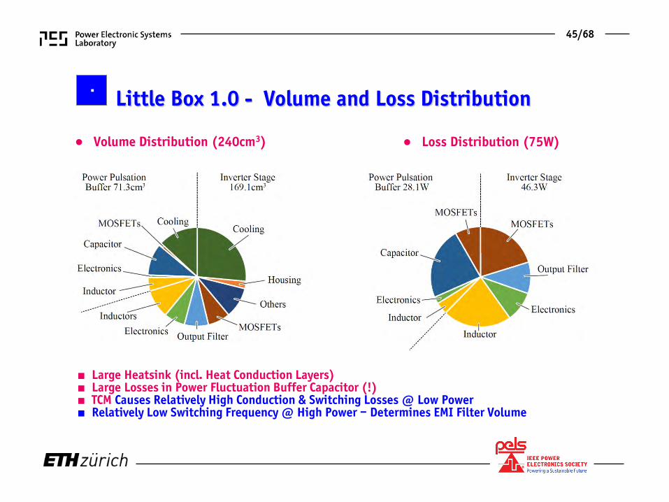
Little Box 1.0 - Volume and Loss Distribution
Large Heatsink (incl. Heat Conduction Layers) Large Losses in Power Fluctuation Buffer Capacitor (!) TCM Causes Relatively High Conduction & Switching Losses @ Low Power Relatively Low Switching Frequency @ High Power – Determines EMI Filter Volume
Volume Distribution (240cm3) Loss Distribution (75W)
45/68

Other Finalists Topologies
Switching Frequencies Power Density / Efficiency Comparison
Detailed Descriptions: www.LittleBoxChallenge.com
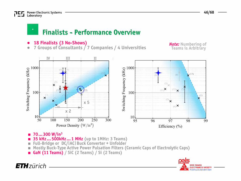
Finalists - Performance Overview 18 Finalists (3 No-Shows) 7 Groups of Consultants / 7 Companies / 4 Universities
70 … 300 W/in3
35 kHz … 500kHz … 1 MHz (up to 1MHz: 3 Teams) Full-Bridge or DC/ AC Buck Converter + Unfolder Mostly Buck-Type Active Power Pulsation Filters (Ceramic Caps of Electrolytic Caps) GaN (11 Teams) / SiC (2 Teams) / Si (2 Teams)
46/68
x 2
x 5
IV III II
Note: Numbering of
Teams is Arbitrary. .

Finalists - Performance Overview 18 Finalists (3 No-Shows) 7 Groups of Consultants / 7 Companies / 4 Universities
47/68
(1) Virginia Tech (2) Schneider Electric (3) EPRI (Univ. of Tennessee) (4) Venderbosch (5) Energy Layer
(6) ETH Zurich (7) Rompowe r (8) Tommasi-Bailly (9) Red Electric Devils (10) AHED
(11) FH IISB (12) Univ. of Illinois (13) AMR (14) OKE (15) Cambridge Magnetics
x 2
x 5
IV III II
Note: Numbering of
Teams is Arbitrary. .

70 … 300 W/in3
35 kHz … 500kHz … 1 MHz (up to 1MHz: 3 Teams) Full-Bridge or DC/ AC Buck Converter + Unfolder Mostly Buck-Type Active Power Pulsation Filters (Ceramic Caps of Electrolytic Caps) GaN (11 Teams) / SiC (2 Teams) / Si (2 Teams)
18 Finalists (3 No-Shows) 7 Groups of Consultants / 7 Companies / 4 Universities
Finalists - Performance Overview
48/68
@ Rated Power
(1) Virginia Tech (2) Schneider Electric (3) EPRI (Univ. of Tennessee) (4) Venderbosch (5) Energy Layer (6) ETH Zurich (7) Rompowe r (8) Tommasi-Bailly (9) Red Electric Devils (10) AHED (11) FH IISB (12) Univ. of Illinois (13) AMR
Note: Numbering of
Teams is Arbitrary. .

Category I: 300 – 400 W/in3 (1 Team) “Over the Edge” Hand-Wound Overstressed & Too Small Electrolytic Capacitors (210uF/400V) No Voltage Margin of Power Semiconductors (450V GaN, Hard Switching) 50V Voltage Source for Semicond. Voltage Stress Reduction Low-Frequ. CM AC Output Component
Alternate Switching of Full-Bridge Legs Input Cap. of Full-Bridge Used for Power Pulsation Buffering 256 W/in3 (400 W/in3 Claimed) / 1MHz Multi-Airgap Toroidal Inductors (3F46, Cp≈1.5pF ) Bare GaN Dies Directly Attached to Pin-Fin Heatsink High Speed Fan (Mini Drone Motor & Propeller)
2x
4x 2x
49/68

Category I: 300 – 400 W/in3 (1 Team) “Over the Edge” Hand-Wound Overstressed Electrolytic Capacitors (210uF (?)/400V) No Voltage Margin of Power Semiconductors (450V GaN, Hard Switching) 50V Voltage Source for Semicond. Voltage Stress Reduction
Alternate Switching of Full-Bridge Legs Input Cap. of Full-Bridge Used for Power Pulsation Buffering 256 W/in3 (400 W/in3 Claimed) / 1MHz Multi-Airgap Toroidal Inductors (3F46, Cp≈1.5pF ) Bare Dies Directly Attached to Pin-Fin Heatsink High Speed Fan (Mini Drone Motor & Propeller)
50/68
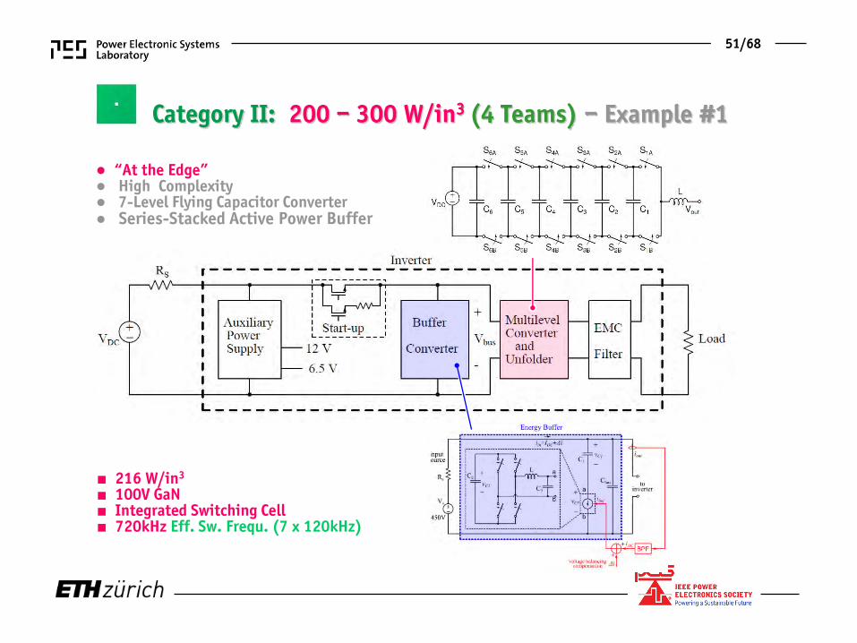
Category II: 200 – 300 W/in3 (4 Teams) – Example #1
“At the Edge” High Complexity 7-Level Flying Capacitor Converter Series-Stacked Active Power Buffer
216 W/in3
100V GaN Integrated Switching Cell 720kHz Eff. Sw. Frequ. (7 x 120kHz)
51/68
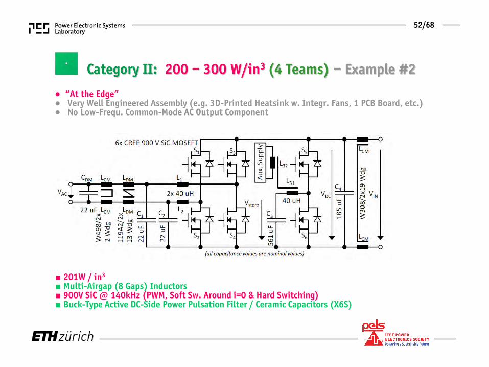
Category II: 200 – 300 W/in3 (4 Teams) – Example #2
“At the Edge” Very Well Engineered Assembly (e.g. 3D-Printed Heatsink w. Integr. Fans, 1 PCB Board, etc.) No Low-Frequ. Common-Mode AC Output Component
201W / in3
Multi-Airgap (8 Gaps) Inductors 900V SiC @ 140kHz (PWM, Soft Sw. Around i=0 & Hard Switching) Buck-Type Active DC-Side Power Pulsation Filter / Ceramic Capacitors (X6S)
52/68

Category III: 100 – 200 W/in3 (8 Teams) – Example “Advanced Industrial” Sophisticated 3D Sandwich Assembly incl. Cu Honeycomb Heatsink Shielded Multi-Stage EMI Filter @ DC Input and AC Output No Low-Frequ. Common-Mode AC Output Component
143 W/in3
GaN @ ZVS (35kHz…240kHz) 2 x Interleaving for Full-Bridge Legs Buck-Type DC-Side Active Power Pulsation Filter (<150μF)
53/68

Category III: 100 – 200 W/in3 (8 Teams) – Example “Advanced Industrial” Sophisticated 3D Sandwich Assembly incl. Cu Honeycomb Heatsink Shielded Multi-Stage EMI Filter @ DC Input and AC Output No Low-Frequ. Common-Mode AC Output Component
143 W/in3
GaN @ ZVS (35kHz…240kHz) 2 x Interleaving for Full-Bridge Legs Buck-Type DC-Side Active Power Pulsation Filter (<150μF)
54/68

Category IV: 50 – 100 W/in3 (1 Team) “Industrial” 400Vmax Full-Bridge Input Voltage DC-Link Cap. Used as Power Pulsation Buffer (470uF) GaN Transistors / SiC Diodes (400kHz DC/DC, 60kHz DC/AC) Multi-Stage EMI Filter @ AC Output and LCM + Feed-Trough CCM @ DC Inp. (Not Shown)
≈70 W/ in3
98% CEC (Weighted) Efficiency 4.4% DC Input Current Ripple
54°C Surface Temp. / Cooling with 10 Mirco-Fans
55/68

Competition Conclusions Key Technologies
Power Density Limit

Little Box Challenge Summary
200W/in3 (12kW/dm3) Achievable
fs < 150kHz (Constant) SiC (Not GaN) ZVS (Partial, i.e. Around i=0) Full-Bridge Output Stage Active Power Pulsation Buffer (Buck-Type, X6S Cap.) Conv. EMI Filter Structure Multi-Airgap Litz Wire Inductors DSP Only (No FPGA)
Overall
Engineering “Jewels” No (Fundamentally) New Approach / Topology Passives & 3D-Packaging are Finally Defining the Power Density Careful Heat Management (Adv. Heat Sink, Heat Distrib., 2-Side Integr. Cooling, etc.) Careful Mechanical Design (3D-CAD, Single PCB, Avoid Connectors, etc.) Clear Power Density / Efficiency Trade-Off
56/68
100+ Teams 3 Members / Team, 1 Year
300 Man-Years 3300 USD / Man-Year

Little Box 2.0
DC/ACConverter + Unfolder PWM vs. TCM incl. Interleaving ηρ-Pareto Limits for Non-Ideal Switches Final 3D-CAD Preliminary Exp. Results
250 W/in3

Little Box 2.0 – New Converter Topology (1)
57/68
vC0 Easy to Generate/Control Higher Conduction Losses Due to FB-Unfolder Lower CM-Noise (DC & n x 120Hz-Comp.) CCM=700nF Allowed for 50mA Gnd Current
vAC1 More Difficult to Generate/Control Lower Conduction Losses Higher CM-Noise (DC and n x 120Hz-Comp.) CCM=150nF Allowed for 50mA Gnd Current
Alternative Converter Topology Only Single HF Bridge Leg + 60Hz-Unfolder DC/AC- Buck Converter + Full-Bridge Unfolder OR HF Half-Bridge & Half-Bridge Unfolder

Little Box 2.0 – New Converter Topology (2) Alternative Converter Topology - DC/AC- Buck Converter + Unfolder 60Hz-Unfolder (Temporary PWM for Ensuring Continuous Current Control) TCM or PWM of DC/AC- Buck-Converter
Full Optimization of All Converter Options for Real Switches / X6S Power Pulsation Buffer
58/68

Little Box 2.0 – Multi-Objective Optimization DC/AC- Buck Converter (Single Bridge Leg) + Unfolder & PWM Shows Best Performance Full-Bridge Would Employ 2 Switching Bridge Legs - Larger Volume & Losses Interleaving Not Advantageous – Lower Heatsink Vol. but Larger Total Vol. of Switches and Inductors
ρ= 250W/in3 (15kW/dm3) @ η= 98% Efficiency Achievable for Full Optimization
-- 4D-Interleaving Considered for TCM
59/68

Little Box 2.0 – Control Structure
Each Stage (Buck & Unfolder) Controlled with Cascaded Current and Voltage Loop Without Switching of Unfolder Control Like for Conventional Boost PFC Rectifier
60/68

3D-CAD Construction
of the Final System
250 W/in3

Little Box 2.0 – Final Mechanical Construction (1)
61/68
60 mm x 50 mm x 45 mm = 135 cm3 (8.2in3 ) 14.8 kW/dm3 (243 W/in3)
PPB Capacitor Output Filter

62/68
Little Box 2.0 – Final Mechanical Construction (2)
60 mm x 50 mm x 45 mm = 135 cm3 (8.2in3 ) 14.8 kW/dm3 (243 W/in3)
PPB Capacitor
Heat Sink + Fans
Output Filter
63/68
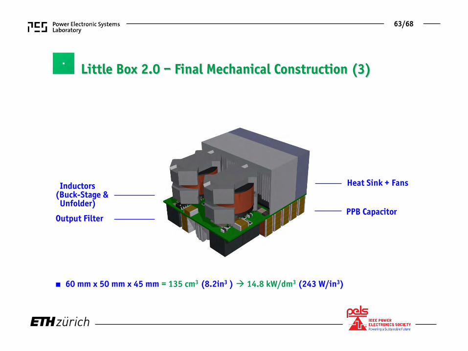
Little Box 2.0 – Final Mechanical Construction (3)
60 mm x 50 mm x 45 mm = 135 cm3 (8.2in3 ) 14.8 kW/dm3 (243 W/in3)
PPB Capacitor
Inductors (Buck-Stage & Unfolder)
Heat Sink + Fans
Output Filter
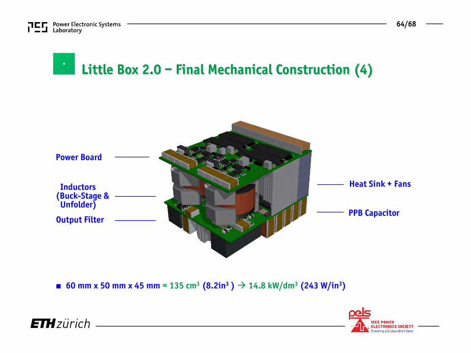
64/68
PPB Capacitor
Heat Sink + Fans
Power Board
60 mm x 50 mm x 45 mm = 135 cm3 (8.2in3 ) 14.8 kW/dm3 (243 W/in3)
Little Box 2.0 – Final Mechanical Construction (4)
Inductors (Buck-Stage & Unfolder)
Output Filter
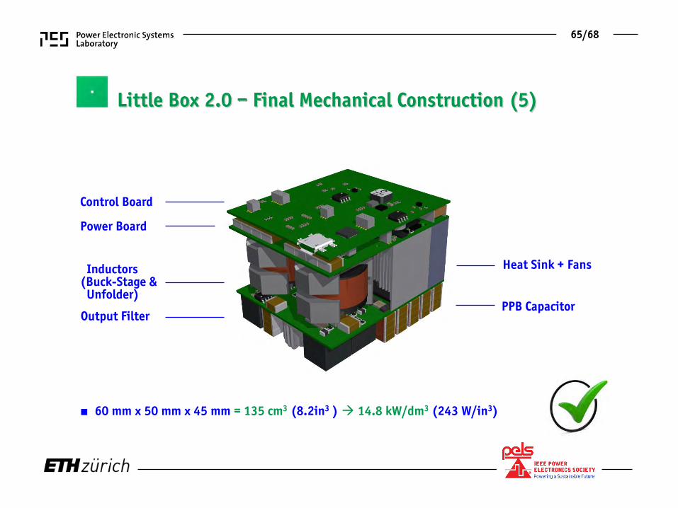
65/68
Control Board
Little Box 2.0 – Final Mechanical Construction (5)
PPB Capacitor
Heat Sink + Fans
Power Board
60 mm x 50 mm x 45 mm = 135 cm3 (8.2in3 ) 14.8 kW/dm3 (243 W/in3)
Inductors (Buck-Stage & Unfolder)
Output Filter

Capacitive Load
Little Box 2.0 – Measured Waveforms
DC/|AC| Buck-Stage Output Voltage & Inductor Current
Inductive Load Resistive Load
66/68

Little Box 2.0 – Preliminary Efficiency Measurements
Performance of First DC/AC- Buck Converter + Unfolder Prototype PWM Operation Without Power Pulsation Buffer
98% for Res. Load Achievable if Cond. Losses of PCB (Copper Cross Sect.) & Unfolder (Rds,on) are Red.
67/68

Source: whiskeybehavior.info
Overall Summary

Performance Limits / Future Requirements
New Integr. Control Circuits and i=0 Detection for Sw. Frequency >1MHz Integrated Gate Drivers & Switching Cells High Frequency Low Loss Magnetic Materials High Bandwidth Low-Volume Current Sensors Low Loss Ceramic Capacitors Tolerating Large AC Ripple Passives w. Integr. Heat Management and Sensors 3D Packaging
New U-I-Probes Required for Ultra-Compact Conv. R&D Specific Systems for Testing Devices Equipped with Integr. Measurement Functions Convergence of Sim. & Measurem. Tools Next Gen. Oscilloscope New Multi-Obj. Multi-Domain Simulation/Optim. Tools
68/68
220…250W/in3 for Two-Level Bridge Leg + Unfolder 250…300W/in3 for Highly Integrated Multi-Level Approach Isol. Distance Requirements Difficult to Fulfill Fulfilling Industrial Inp. Overvoltage Requirem. would Signific. Reduce Power Density
Low Frequency (20kHz…120kHz) SiC vs. HF (200kHz…1.2MHz) GaN Multi-Cell Concepts for LV Si (or GaN) vs. Two-Level SiC (or GaN)

Thank You !