the em side–channel(s):attacks and assessment methodologies...
TRANSCRIPT

The EM Side–Channel(s):Attacks and AssessmentMethodologies
Dakshi Agrawal Bruce Archambeault Josyula R. Rao
Pankaj RohatgiIBM Watson Research Center
P.O. Box 704Yorktown Heights, NY 10598
email: agrawal,barch,jrrao,[email protected]
Abstract
We present a systematic investigation of the leakage of compromising information via electro-magnetic (EM) emanations from chipcards and other devices. This information leakage differssubstantially from and is more powerful than the leakage from other conventional side-channelssuch as timing and power. EM emanations are shown to consist of a multiplicity of compro-mising signals, each leaking somewhat different information. Our experimental results confirmthat these signals could individually contain enough leakage to break cryptographic implementa-tions and to defeat countermeasures against other side-channels such as power. Using techniquesfrom Signal Detection Theory, we also show that generalized and far more devastating attackscan be constructed from an effective pooling of leakages from multiple signals derived from EMemanations.
The magnitude of EM exposure demands a leakage assessment methodology whose correctnesscan be rigorously proved. We define a model that completely and quantitatively bounds theinformation leaked from multiple (or all available) EM side-channel signals in CMOS devices anduse that to develop a practical assessment methodology for devices such as chipcards.
1 Introduction
Side–channel cryptanalysis has been used successfully to attack many cryptographic implementations[10, 11]. Most of the publicly available literature on side–channels deals with attacks based on timingor power. While it is rumored that there is a large body of classified literature on exploiting leakagesdue to electromagnetic (EM) emanations, there is scant information about this in the public domain.
With the recent declassification of portions of the TEMPEST documents [7], initial reports byJ. J. Quisquater[12] and publication of some EM attacks [9], an awareness of the potential of theEM side–channel is developing. However, some basic questions remain unanswered. For instance,what are the causes and types of EM emanations? How does information leaked via EM emanationscompare with leakages from other side–channels? What implementations are vulnerable to EM side–channel attacks? Can the EM side–channel overcome countermeasures designed to provide protectionagainst other side–channel attacks? Given the set of EM emanations available to an adversary, is it
1

possible to bound the net information leaked in an information theoretic sense, i.e., independent of thecomputational and signal processing abilities of the adversary? With questions such as these in mind,we conducted a systematic investigation of EM side–channel leakage from chipcards. In this paper,we address each of these basic questions.
A crucial insight from our investigation is that the output of even a single EM sensor consists ofmultiple compromising signals of different types, strengths and information content. Of these, highamounts of compromising information is usually found in very low energy signals. It is thereforeimperative that signals be separated early in the acquisition process to avoid loss of low energy signalsdue to precision limits of signal capturing equipment. Here, we differ from [9] where signals areobtained from different micro–antenna positions, but nevertheless the output of the sensor is treatedas a single signal. While careful positioning of a micro–antenna can acquire and emphasize some lowenergy signals, without further signal separation, some high information, low energy signals can stillbe overwhelmed by adjacent lower information, higher energy sources.
We describe the basis for this insight in Section 2. We first discuss the causes and types of variousEM signals that we observed using several sensors. These include several unexpected signals that areeasy to overlook if one does not suspect their existence. For instance, despite extensive work with powersignals, researchers had so far missed the very faint, but far more compromising amplitude modulatedEM signals present in the power line and other conductors attached to the chipcard. We then describethe experimental equipment, techniques used to extract compromising signals and empirical evidencethat confirms that different signals carry different information.
Since EM emanations permit the use of several conductive and radiative sensors each containingmultiple signals, an adversary has a wide array of compromising signals at his disposal. In situationswhere the power side–channel is not available, e.g., the power supply is filtered or the attack has tobe mounted from a distance, the advantages of using EM are obvious. The more pertinent questionis whether this abundance of signals provides any practical advantage in using the EM side–channelin situations where the traditional side–channels such as power are also available. This question isespecially appropriate given the high cost of some EM equipment.
In Section 3, we answer this question in the affirmative. We demonstrate that even low cost EMequipment which can collect only one signal at a time is quite effective against fielded devices. Forall devices, we obtained signals which were amenable to attacks such as simple and differential elec-tromagnetic attacks (SEMA and DEMA [12]). We were able to successfully attack cryptographicimplementations of block ciphers such as DES, public key schemes such as RSA on chipcards and SSLAccelarators and even proprietary algorithms such as the prescribed COMP128 GSM authenticationscheme. More interestingly, in many devices we could obtain EM signals in which some leakages wereexcessive, i.e., they had a far superior signal to noise ratio than in the power signal 1. These excessiveleakages form the basis of devastating attacks against fielded systems including those resistant to poweranalysis attacks. We present such attacks against two major classes of power analysis countermea-sures [11, 1, 6] implemented on a test system 2. We show that the attack against the secret–sharingcountermeasures of [1, 6] is powerful enough to work even in the case when the code of a protectedimplementation is unknown.
Despite their effectiveness, our low–cost attacks provide only a glimpse of what is possible. Wecollected only one signal at a time and followed the intuitive strategy of using the signal source with
1Most devices have classes of “bad” instructions with excessive leakages.2A test system was chosen to avoid disclosing weaknesses of commercially deployed systems.
2

the best signal to noise ratio. A better funded adversary would deploy several sensors3 to collectmultiple signals. More importantly, he will use techniques from Signal Detection Theory to launch farmore sophisticated and devastating attacks. As we show, such attacks can be highly efficient requiringgreatly reduced number of samples: more than an order of magnitude less than traditional schemesthat employ simple intuitive statistics such as the mean signal and the L2–norm. The theory alsoprescribes better adversarial strategies. For instance, we show that if only two sensor signals can becollected, the intuitive strategy of picking the two signals with the best signal–to–noise ratio can be sub–optimal. Therefore, for the purpose of determining vulnerabilities and for devising countermeasures,it is essential to have a formal model to understand and assess how such an adversary can best exploitthe wide array of signals available from the sensors that he can deploy.
Formulating such an adversarial model has numerous pitfalls. Ideally, the model should capture thestrongest side–channel attacks possible on an implementation of a cryptographic algorithm involvingsecret data. While it is easy to define such a model, using it to assess vulnerabilities will inevitablymove the focus from information leakage from sensors to the analysis of algorithm and implementationspecific attacks that various adversaries with a wide spectrum of capabilities could employ.
To refocus the attention on information extractable from the sensors, our model will focus only onelementary leakages, i.e., information leaked during elementary operations of CMOS devices. Such afocus is not limiting in the information–theoretic sense as we prove that all side–channel informationleakage in a computation can be viewed as a composition of elementary leakages from all of its elemen-tary operations. The model of elementary leakages maps directly to first order differential side–channelattacks (attacks in which different cycles of each computation are considered independently, such asDEMA) on implementations. These elementary leakages also serve as basic building blocks for thedesign and analysis of more sophisticated, algorithm and implementation specific attacks.
In Section 4, we describe the adversarial model in terms of hypothesis testing. The model providesa formal way of comparing efficacies of various signal selection and processing techniques that can beapplied by resource limited adversaries in terms of success probabilities achieved. It also provides aframework to quantify and bound the information leakage from the sensors in terms of the best errorprobability achieved by an all–powerful adversary. Using this model, we describe some sophisticatedand counter-intuitive strategies, based on Signal Detection Theory, that a resource limited adversarycan use to launch devastating attacks. Next, we describe a methodology based on the same Theorythat addresses the issue of assessing any type of leakage in an information—theoretic sense. Themethodology permits the computation of bounds on the best error probability achieved by an all–powerful adversary. While such an assessment is impractical for arbitrary devices, it is feasible for thepractically important case of chipcards with small word lengths. We then show (Theorem 1) that suchan assessment also completely captures side–channel leakages in arbitrary attacks on implementations.
2 EM Signals and Leakages
This section describes the origin and types of various EM signals that we have observed4. We provideempirical evidence that confirms that different signals carry different information and describe theexperimental equipment and techniques used to extract various compromising signals.
3In practice, any adversary will be limited by the number and types of sensors that he can deploy.4While there is an obvious overlap with the declassified TEMPEST documents (NACSIM 5000) [13], we only describe
what we have verified in our investigations.
3
2.1 Origin of EM Emanations
EM emanations arise as a consequence of current flows within the control, I/O, data processing orother parts of a device. These flows and resulting emanations may be intentional or unintentional.Each current carrying component of the device not only produces its own emanations based on itsphysical and electrical characteristics but also affects the emanations from other components due tocoupling and circuit geometry.
Of these numerous emanations, those induced by data processing operations carry the most com-promising information. In CMOS devices, ideally, current only flows when there is a change in the logicstate of a device. In addition, all data processing is typically controlled by a “square-wave” shapedclock. Each clock edge triggers a short sequence of state changing events and corresponding currents inthe data processing units. The events are transient and a steady state is achieved well before the nextclock edge. At any clock cycle, the events and resulting currents are determined by a small numberof bits of the logic state of the device, i.e., one only needs to consider the active circuits during thatclock cycle. These bits, termed as relevant bits in [1], constitute the relevant state of the device. Thesecurrents result in many compromising emanations in several unintended ways. Such emanations carryinformation about the currents and hence the events and relevant state of the device. In practice,CMOS devices are not ideal there may be many very small leakage currents in inactive parts of thecircuit as well. These can be approximated as a small gaussian noise term having negligible correlationwith any particular inactive part of the circuit.5
Since each active component of the device produces and induces various types of emanations, thesemultiple emanations provide multiple views of events unfolding within the device. Views emphasizingdifferent active components can be obtained by using different types and positions of sensors [9, 12] oreven by focusing on different types of emanations that can be captured by a single sensor as we willshow in this paper. This is in sharp contrast to the power side–channel where there is only a singleaggregated view of net current inflow. The presense of multiple views make the EM side–channel(s)much more powerful than the power side–channel.
2.2 Types of EM Emanations
There are two broad categories of EM emanations:1. Direct Emanations: These result from intentional current flows. Many of these consist ofshort bursts of current with sharp rising edges which result in emanations observable over a widefrequency band. Often, components at the higher frequencies prove more useful to the attacker dueto overwhelming noise and interference prevalent in the lower frequency bands. In a complex circuits,isolating direct emanations can be difficult and may require use of tiny field probes positioned veryclose the signal source and/or special filters so as to minimize interference from other signal sources;getting good results may necessisate having to decapsulate the chip packaging [9, 12].2. Unintentional Emanations: Increased miniaturization and complexity of modern CMOS de-vices results in electrical and electromagnetic coupling between components in close proximity. Suchcouplings, while inconsequential from the perspective of a circuit designer, provide a rich source ofcompromising emanations to the attacker. These emanations manifest themselves as modulations ofcarrier signals generated, present or “introduced” within the device. One strong source of carrier
5This fact is well known in DPA literature where expermentally it is observed that algorithmic bits are significantycorrelated to the total current only during the times when they are actively involved in a computation.
4

signals is the harmonic–rich “square–wave” clock signal6 propagated throughout the device. Othersources include communication related signals. Some of the ways in which modulation occurs include:a. Amplitude Modulation: Non-linear coupling between a carrier signal and a data signal re-sults in the generation and emanation of an Amplitude Modulated (AM) signal. The data signal canbe extracted by using a receiver tuned to the carrier frequency and then performing AM demodulation.
b. Angle Modulation: Coupling of circuits also results in Angle Modulated Signals (FM or Phasemodulation). For instance, while signal generation circuits should ideally be completely decoupledfrom data processing circuits, this is rarely achieved in practice. For example, if these circuits drawupon limited energy source, the generated signal, very often, is angle modulated by the data signal.The data signal is recoverable by angle demodulation of the generated signal.
Exploiting modulated carriers can be easier and more effective that trying to work with directemanations. Firstly, some modulated carriers could have substantially better propogation than directemanations, permitting effective EM attacks without resorting to invasive techniques and attacks thatcan be performed at a distance. E.g, all attacks decribed in this paper do not require any intru-sive/invasive techiques or fine grained positioning of probes. Secondly, careful field probe positioningcannot separate two sources of direct emanations in close proximity, whereas such sources may beeasily separable due to their differing interaction with the carriers present in the vicinity.
2.2.1 Emperical Results
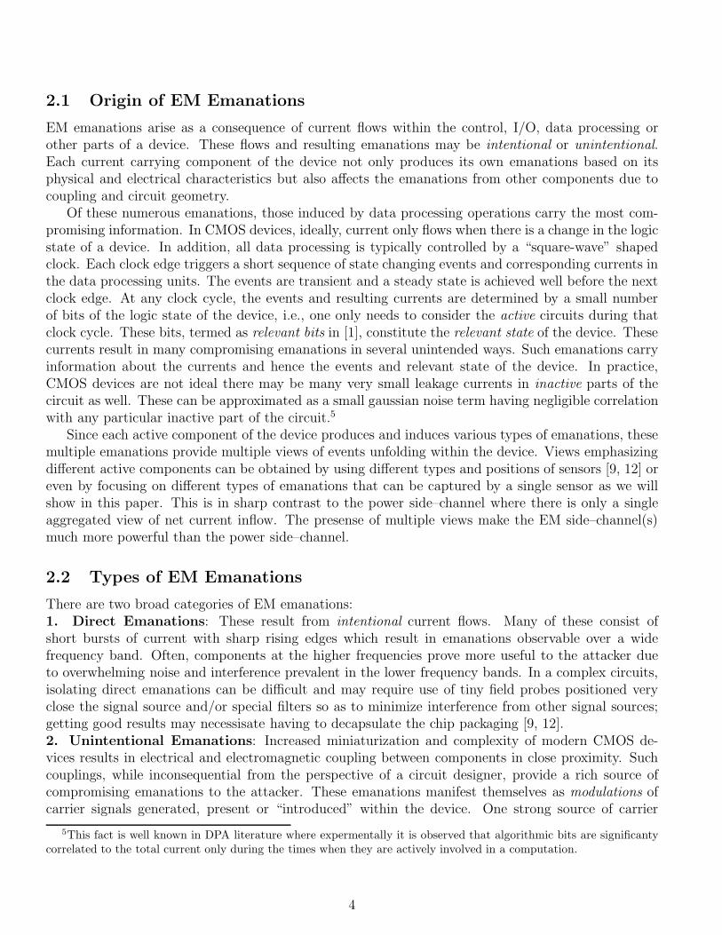
We now present emperical results which illustrate the types of emanations discussed above.Experiment 1: Direct Emanations: We used a relatively recent smart card that we call smartcardA (to protect vendor identity7), which we programmed to enter a 13 cycle infinite loop, running onthe externally supplied 3.68MHz clock. A handmade near-field probe (a small metal plate attachedto a co-axial cable) was placed close to the plastic at the back of smart card, near the chip. Thesignal was amplified using a wideband amplifier (0.1-500Mhz) and 500K sample points (representingapprox 284 iterations of the loop) were collected with an 8-bit, 500Mhz digital scope. In the timedomain, this baseband (band centered at 0Mhz) direct emanations signal, looked like a differentiatedform of the external clock and provided no visual indication of a loop execution. The situation canbe best analysed in the frequency domain. The signal received by the probe consists of the signal ofinterest, i.e., a periodic signal corresponding to a loop iteration at a frequency 283Khz (3.68Mhz/13),and other signals from the chip and its vicinity such as the clock (periodic with freq 3.68Mhz) andother aperiodic noise. Capturing the received signal with a limited resolution (8-bit) scope furtherintroduces quantization noise. Figure 1 plots the FFT of the captured baseband signal (where theY-axis is the magnitude8 and the X-axis is the frequency in KHz). The large spikes below 100 MHz arethe high energy harmonics of the clock signal and tiny spikes sprinkled between them are other typesof direct and unintentional emanations which are of interest. Very little signal is noticeable above
6Theoretically a perfectly symmetric, perfectly square signal consists of the fundamental frequency and all the oddharmonics with progressively diminishing strengths. In practice, the clock signal is always imperfect.
7Smartard A is 6805-based, uses 0.6 micron triple metal technology with an optional variable internal clock as onedefence against DPA.
8In all our figures, signal or FFT magnitudes should be treated as relative quantities, since we don’t track the absolutequantities involved as the signals typically undergo analog amplification/processing steps before being captured by ourscopes with 8-bit or 12-bit resolution. We typically set the scope sensitivity so that the received signal covers most ofthe available 8-12 bit dynamic range.
5
0 0.5 1 1.5 2
x 105
0.5
1
1.5
2
2.5
3
3.5
4
x 106
Figure 1: FFT of baseband signal from Experiment 1 with Smartcard A
6

0 2000 4000 6000 8000 10000 12000 14000 16000 18000 20000
0
1
2
3
4
5
6
7
Figure 2: Log of FFT in the region 0-20Mhz from Experiment 1 with Smartcard A
7
125 MHz, essentially because the signal strenghts here are much lower than in the 0-100Mhz bandand these signals have been overwhelmed by quantization noise. In the linear scale, the fact that thecard is executing a 13-cycle loop is not apparent. On a log (base 10) scale, zooming into the regionfrom 0 to 20Mhz, in Figure 2 one can indeed see the signal of interest at 283Khz and its harmonics,interspersed between the clock signal and its harmonics. Note that the use of a large time window(284 iterations of the loop) helps in detecting these periodic signals since the aperiodic noise from thechipcard, environment and quantization gets reduced due to averaging. Since direct emanations ofinterest are more than an order of magnitude smaller than other interfering signals, exploiting themin the presence of quantization noise will require the use of smaller, better and carefully positionedprobes (possibly after decapulating the chip) to emphasize these signals and to reduce interferencefrom other signals. In addition a specially designed comb filter or some other method could be used tosuppress the contribution from the clock signal. Since the results of using this approach have alreadybeen publicized [9, 12], we focus mainly on a different approach that we employed based on exploitingunintentional emanations.
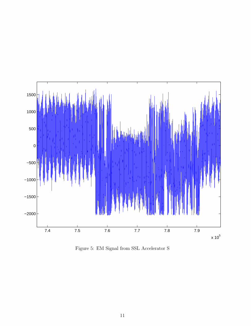
Experiment 2: Unintentional AM emanations: Next we took the same setup as in Experiment 1, butnow the output of the probe was sent to an AM receiver, tuned to the 41’st clock harmonic at 150.88Mhz with a band of 50Mhz. The demodulated output from the receiver was sampled with a 12-bit100Mhz scope 9 and 100K sample points representing approximately 284 iterations were collected.Figure 3 (where the Y-axis is the magnitue and the X-axis is the frequency in KHz) plots the FFT ofthis signal. Now, even in this linear scale, the signal of interest, i.e., the 283KHz signal correspondingto the loop and its harmonics is clearly visible among the signal corresponding to the clock harmonicsand the loop structure was also visible in the time-domain. Notice that these greatly improved resultswere obtained using the same sensor setting as in Experment 1, and with the same number of loopiterations. Note that we are also operating in a part of the spectrum which did seem to even havemuch signal according to Figure 1; the signals in this band were overwhelmed by the quantizationnoise introduced when we attempted to capture the baseband signal.Experiment 3: Unintentional Far–Field AM Emanations: We examined emanations from an Intel–based server containing a commercial, PCI bus based SSL accelerator S10. We programmed the serverto repeatedly invoke S to perform a 2048 bit exponentiation with a single–nibble exponent. SeverlAM modulate carriers, including those at multiples of the 33Mhz PCI clock frequency and otherweaker intermodulated carriers were found. In the near field, sevaral AM-demodulated carriers leakedinformation about the internal structure of the exponentiation even from a single sample, thus enablinga variety of attacks. Some of the stronger information bearing signals, e.g., carriers at multiples of the33MHz PCI clock propagate to distances upto forty feet but the quality of the received informationdegrades as a function of the distance (due to inverse-square law) and the bandwidth (due to thethermal noise floor) being used. Figure 5 plots a signal (amplitude vs. time in ms) captured by alog–periodic antenna 15 feet away using the 299MHz carrier and 1MHz bandwidth. The invocationsof S is clearly visible as a region from 7.55ms to 7.91ms where the amplitude goes below -1000. At thisresolution, the macro structures within the exponentiation are already visible. At higher resolutions,there is enough information to enable template attacks [2].Experiment 4: Unintentional Angle Modulated emanations: Next we turned on the variable internalclock DPA protection mechanism in Smartcard A and kept everything else, including the loop and the
9One advantage of using low sampling rate is that higher precision sampling equipment is available10S is rated to perform 200, 1024-bit CRT based RSA private key ops/s.
8

0.5 1 1.5 2 2.5 3 3.5 4 4.5 5
x 104
2
4
6
8
10
12
14
16
18
x 106
Figure 3: FFT of demodulated signal (150.88 Mhz carrier, 50Mz band) in Experiment 2 with SmartcardA
9

625 630 635 640 645 650 655 660
0
5
10
15
20
x 105
Figure 4: Two FFTs showing differce in loop frequency for LSB=0 and LSB=1 for smartcard A
10
7.4 7.5 7.6 7.7 7.8 7.9
x 105
−2000
−1500
−1000
−500
0
500
1000
1500
Figure 5: EM Signal from SSL Accelerator S
11

sensor position the same as Experiment 1. One of the instructions in the 13-cycle loop was to load auser supplied byte B from RAM to accumulator. We found a carrier where by AM-demodulation onecould clearly see the card executing a loop. We experimented with different values of the byte B andmade the following surprising observation: The average frequency of the 13-byte loop was dependenton the least significant bit (LSB) of B but not on other bits. This is shown in Figure 4, where isthe magnitude of FFT of the EM output for two different cases (with the X axis being frequency inKHz). The first case (shown by a broken line) shows the loop frequency with the LSB of B being1 and in the second case (shown by a solid line) the loop frequency executes with LSB of B being0. When the LSB is 1 the loop runs slower. This is due to some coupling between the LSB of thedata line and the circuitry generating the internal clock. Although the clock timing itself varies veryoften, when there is a 1 bit on the line, we found that this intrinsic variation gets biased towardsslowing down the clock for a couple of subsequent cycles. We speculate that this is becuause the clockcircuitry draws energy from the same source as some other circuitry affected by LSB. Thus, angledemodulation, e.g., FM demodulation, turns out to be a good avenue for attacking smartcard A usingLSB based hypothesis, effectively transforming a countermeasure into a liability. Another advantageof such angle demodulation based attacks is that the internal clock signal is very strong and observableat a distance.
2.3 Information Leakage across EM Spectrum
In this section we provide experimental evidence to reinforce a central theme of this paper, i.e., theoutput of even a single wideband EM sensor logically consists of multiple EM signals each carryingqualitatively different compromising information. In addition, certain leakages can be substantiallysuperior in some EM signals as compared to the power consumption signal.
Whereas the presence and locations of certain types of EM signals (e.g., angle modulated carriers,intermodulated carriers etc) are very device dependent, our experiments show that universally, AMcarriers at harmonics of the clock frequency are a rich and easily accessible source of compromisinginformation. For smart cards, since the fundamental freqency is so low, the intermediate harmonics areusually the best. Lower harmonics suffer from excessive noise and interference and higher harmonicstend to have extremely low signal strength11.
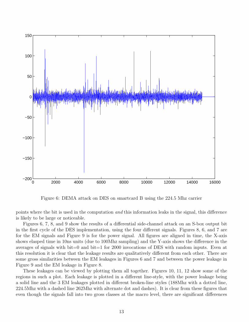
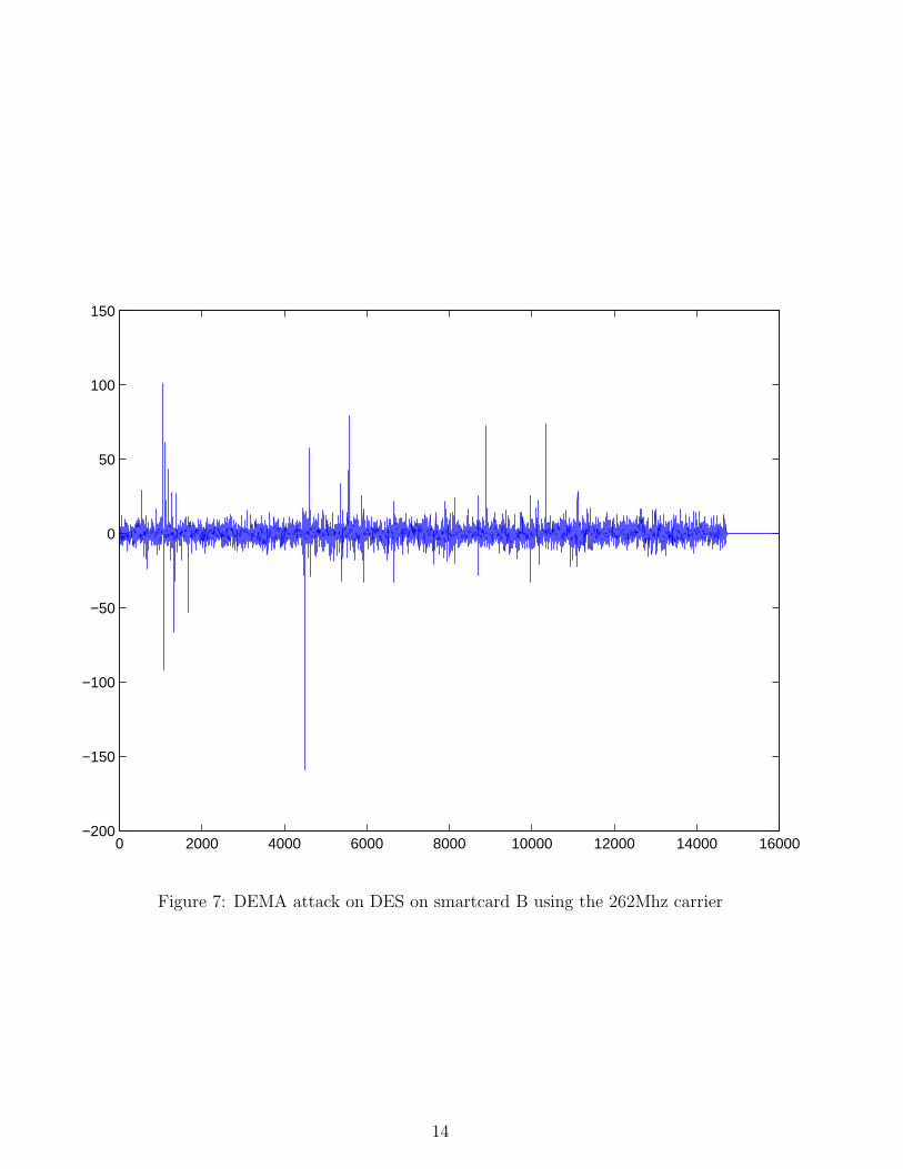
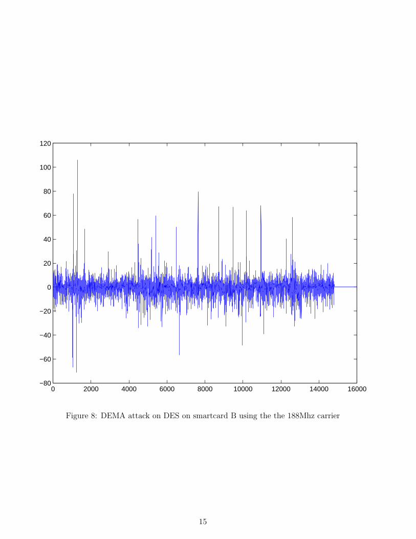
In this section, we examine the leakage of information from four types of signals obtained froma smartcard, which we call smartcard B (to protect vendor identity12), while it performed DES insoftware with no power analysis countermeasures, except for the internal noise generators being on.The smartcard ran on the 3.68Mhz external clock. Three of these signals were obtained by AMdemodulating the output of a near field probe placed as in Experiment 1, at three different intermediatecarrier frequencies (50Mhz bands around 188Mhz, 224.5 and 262Mhz). The fourth signal was the powerconsumption signal. All signals were collected by a 12-bit, 100Mhz digital scope.
It is well known that plotting the results of a differential side channel attack launched against a bitvalue used in a computation is a good way to assess the leakage of the bit [11]. This is not surprisingsince this plot is essentially the difference between the average of all signals in which the bit is 1 andthe average of all signals in which the bit is 0, plotted against time. At times in the computation wherethis bit is not involved or at points in the computation where this bit is involved but that informationdoes not leak in the side-channel, the value of the difference would be small and not noticeable. At
11This is because clock edges are not very sharp in practice.12Smartcard B is a 6805-based, 0.7micron, double metal technology card with inbuilt noise generators.
12
0 2000 4000 6000 8000 10000 12000 14000 16000−200
−150
−100
−50
0
50
100
150
Figure 6: DEMA attack on DES on smartcard B using the 224.5 Mhz carrier
points where the bit is used in the computation and this information leaks in the signal, this differenceis likely to be large or noticeable.
Figures 6, 7, 8, and 9 show the results of a differential side-channel attack on an S-box output bitin the first cycle of the DES implementation, using the four different signals. Figures 8, 6, and 7 arefor the EM signals and Figure 9 is for the power signal. All figures are aligned in time, the X-axisshows elasped time in 10ns units (due to 100Mhz sampling) and the Y-axis shows the difference in theaverages of signals with bit=0 and bit=1 for 2000 invocations of DES with random inputs. Even atthis resolution it is clear that the leakage results are qualitatively different from each other. There aresome gross similarities between the EM leakages in Figures 6 and 7 and between the power leakage inFigure 9 and the EM leakage in Figure 8.
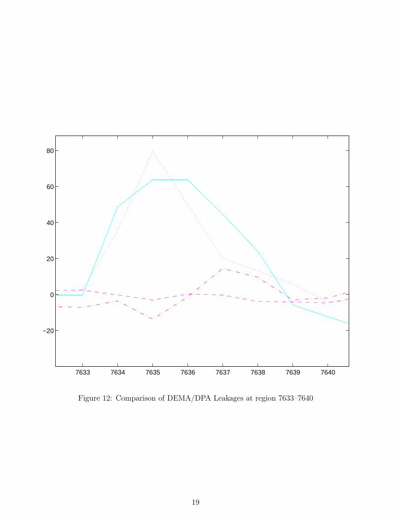
These leakages can be viewed by plotting them all together. Figures 10, 11, 12 show some of theregions in such a plot. Each leakage is plotted in a different line-style, with the power leakage beinga solid line and the 3 EM leakages plotted in different broken-line styles (188Mhz with a dotted line,224.5Mhz with a dashed line 262Mhz with alternate dot and dashes). It is clear from these figures thateven though the signals fall into two gross classes at the macro level, there are significant differences
13
0 2000 4000 6000 8000 10000 12000 14000 16000−200
−150
−100
−50
0
50
100
150
Figure 7: DEMA attack on DES on smartcard B using the 262Mhz carrier
14
0 2000 4000 6000 8000 10000 12000 14000 16000−80
−60
−40
−20
0
20
40
60
80
100
120
Figure 8: DEMA attack on DES on smartcard B using the the 188Mhz carrier
15

0 2000 4000 6000 8000 10000 12000 14000 16000−100
−80
−60
−40
−20
0
20
40
60
80
Figure 9: DPA attack on DES on smartcard B
16

1020 1030 1040 1050 1060 1070 1080 1090 1100 1110
−150
−100
−50
0
50
100
Figure 10: Comparison of DEMA/DPA Leakages at region 1020–1110
even between signals within a class at a cycle level (see Figure 10). Moreover, there are leakages whichappear in EM signals (and sometimes excessively so), which do not appear in the power signal (seeFigure 11). Such leakages are due to a what we will later term as a “bad” instruction. There are alsoleakages which are large in power, but low in some (but not all) EM signals (see Figure 12).
2.4 Propagation and Capture of EM signals
EM signals propagate via radiation and conduction, often by a complex combination of both to even-tually emerge from the device. This naturally suggests the usage of two classes of sensors to capturethe signals that emerge. Radiated signals are best captured by strategically placing near field probesor antennas around the device.
For best results the probes/antennas should be as close as possible or at least in the “near-field”,i.e., no more that a wavelength away13, although a few of the emanations can also be captured fromlarger distances.
Conductive emanations consist of faint currents found on all conductive surfaces or lines attachedto the device. Sometimes, these currents ride on top of stronger, intentional currents flowing withinthe same conductors. Capturing these emanations requires current probes similar to those used forpower analysis and subsequent signal processing to extract them from the stronger signals. In fact, ifthe researchers experimenting with power analysis attacks were to re-analyze the raw signals from theircurrent probes, they will discover that apart from the relatively low frequency, high amplitude powerconsumption signal, there are faint higher frequency AM modulated carriers representing conductiveemanations as well. For example, Figure 13 shows the current signal during 3 rounds of DES insmartcard B captured with 12-bit, 100Mhz scope (amplitude on Y axis, X axis is elasped time in 10nsunits). However, the same power line is also a conductor entering the chip and hence also carries faintcurrents due to conductive EM emanations. Conductive EM emanations at low frequencies will getlost amongst the larger currents driving the card, but it is quite easy to obtain several EM emanationsat higher frequencies. Figure 14 shows one such EM signal extracted from the same power line byAM demodulation of an intermediate frequency carrier during 3 rounds of DES, captured by a 12-bit,100Mhz scope.
We have found that the most effective near field probes are those made of a small plate of a highly
13For emanations at 300 MHz, the wavelength is 1 meter.
17

4482 4484 4486 4488 4490 4492 4494 4496
−150
−100
−50
0
Figure 11: Comparison of DEMA/DPA Leakages at region 4482–4496
18
7633 7634 7635 7636 7637 7638 7639 7640
−20
0
20
40
60
80
Figure 12: Comparison of DEMA/DPA Leakages at region 7633–7640
19

3 4 5 6 7 8 9 10 11
x 104
−1400
−1200
−1000
−800
−600
−400
−200
0
200
400
Figure 13: Baseband Power Signal for 3 rounds of DES on smartcard B
20

1 2 3 4 5 6 7 8 9 10
x 104
−2000
−1500
−1000
−500
0
Figure 14: EM Signal on Power Line for 3 rounds of DES on smartcard B
21

conducting metal like silver or copper. In the far field, we have used both wideband antennas such asbiconical antennas for lower frequencies and log-periodic for higher frequencies. In some cases, once auseful carrier is identified, one can also hand-craft narrowband Yagi antennas to improve its receptionfrom a distance. Although, it is better to shield the equipment from ambient EM emanations, thisshielding does not have to be elaborate; it is far more productive to make sure is no strong source ofthe interfering emissions (in the band of interest) located close the the device to be attacked.
The emanations captured by each sensor need to be processed to extract compromising infor-mation. For direct emanations, filters may suffice. For unintentional emanations, which manifestthemselves as modulations of carrier signals of various frequencies, a wide bandwidth (preferably tun-able) receiver/demodulator is convenient. Examples of such receivers include the R-1550 Receiverfrom Dynamic Sciences [8] and the 8617 Receiver from Watkins–Johnson. Typically, these receivershave a wide frequency range (upto 1GHz) and bandwidth from 40Hz to 200MHz depending on theoptions. If such equipment is not available, one alternative is to use cheaper wideband radio receiverswhich have intermediate frequency output (e.g., ICOM 7000 or 8500), or to even construct using com-monly available low noise electronic equipment such as signal generators, mixers, band pass filters etc ahetrodyning system which will down-convert the band of interest on to a lower intermediate frequency.
The filtered/demodulated signal from a receiver or the intermediate frequency output of a re-ceiver/hetrodyning circuit can be captured by equipment identical to that used for power analysisattacks, such as a digital sampling board and/or oscilloscope, which can have high precision sincesampling rate does not need to be very high. For intermediate frequency output, subsequent process-ing such as additional filtering and demodulation will have to be done in software.
Obtaining multiple EM signals generally requires multiple receivers and signal capturing equipmentbut if very high precision signal capturing equipment is available then one may be able use a smallernumber of receivers and signal capturing equipment by performing signal separation in software aftercapturing emanations within a very wide band. Equipment such as spectrum analyzers are also usefulfor quickly identifying carriers and potentially useful emanations. A useful rule-of-thumb is to expectstrong carriers at odd harmonics of the clock.
3 EM Attacks With Low Cost Equipment
We now present some simple yet remarkably powerful attacks that use low cost equipment. Theseattacks require only one receiver and the capability to capture only one signal at a time. Even withthis restricted setup, one can perform extensive experimentation with a device to identify and assessa large number of EM signals for their leakage characteristics. This enables the design of attacksexploiting each type of observed leakages. The simple and intuitive attack strategy is to pick an EMsignal with the most leakage relative to noise.
As the reader may have anticipated, we found several EM signals for each tested device where theclassical side-channel attacks such as Simple Electromagnetic Attacks (SEMA) and Differential Elec-tromagnetic Attacks (DEMA) [12] could be performed on algorithms like DES. Section 3.1 illustratesresults of such attacks on a chipcard. While these attacks are interesting, by themselves, they do notjustify why EM side-channel(s) should be used in preference to others. A good justification would beif EM leakages were somehow superior, or better still, if they could be used to break implementationssecure against power and timing attacks. Therefore in Section 3.1 we also show that it is indeed thecase for some intructions that we term “bad instructions” and in Section 3.2 we show how these canbe used to defeat power analysis countermeasures.
22

0.5 1 1.5 2 2.5 3 3.5 4 4.5
x 105
−2000
−1500
−1000
−500
0
500
Figure 15: EM Signal showing 16 DES rounds from smartcard B (AM demod 262Mhz carrier, 50Mhzband
3.1 SEMA, DEMA and Bad Instructions
The terms Simple and Differential Electromagnetic Attacks, abbreviated as SEMA and DEMA, wereintroduced by Jean-Jacques Quisquater at numerous rump session talks at Eurocrypt ’00, Crypto ’00and CHES ’00. In this section, we describe some of the SEMA and DEMA results we obtained oncertain chipcards. Our SEMA attack on a chipcard will be based on a “bad instruction”, i.e., aninstruction which leaks much more information in an EM signal than in the power signal. Beforedescribing the attack, we briefly discuss the information present in many compromising EM signals.
3.1.1 Information in Compromising EM Signals
Just as in the power, a compromising EM signal contains information about the computation doneon the chipcard at various levels of granularity. Consider the setup where smartcard B is performingDES in the setup described in Section 2.3 and the EM signal during the computation captured bya 12-bit 100Mhz scope after AM demodulating the probe signal at the 262Mhz carrier with 50Mhz
23
4.5 5 5.5 6 6.5 7 7.5 8 8.5 9 9.5
x 104
−1500
−1000
−500
0
500
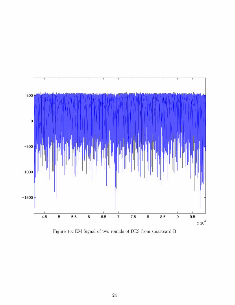
Figure 16: EM Signal of two rounds of DES from smartcard B
24
6.445 6.45 6.455 6.46 6.465 6.47 6.475 6.48 6.485
x 104
−600
−400
−200
0
200
400
Figure 17: EM Signal showing cycle level information from smartcard B
25

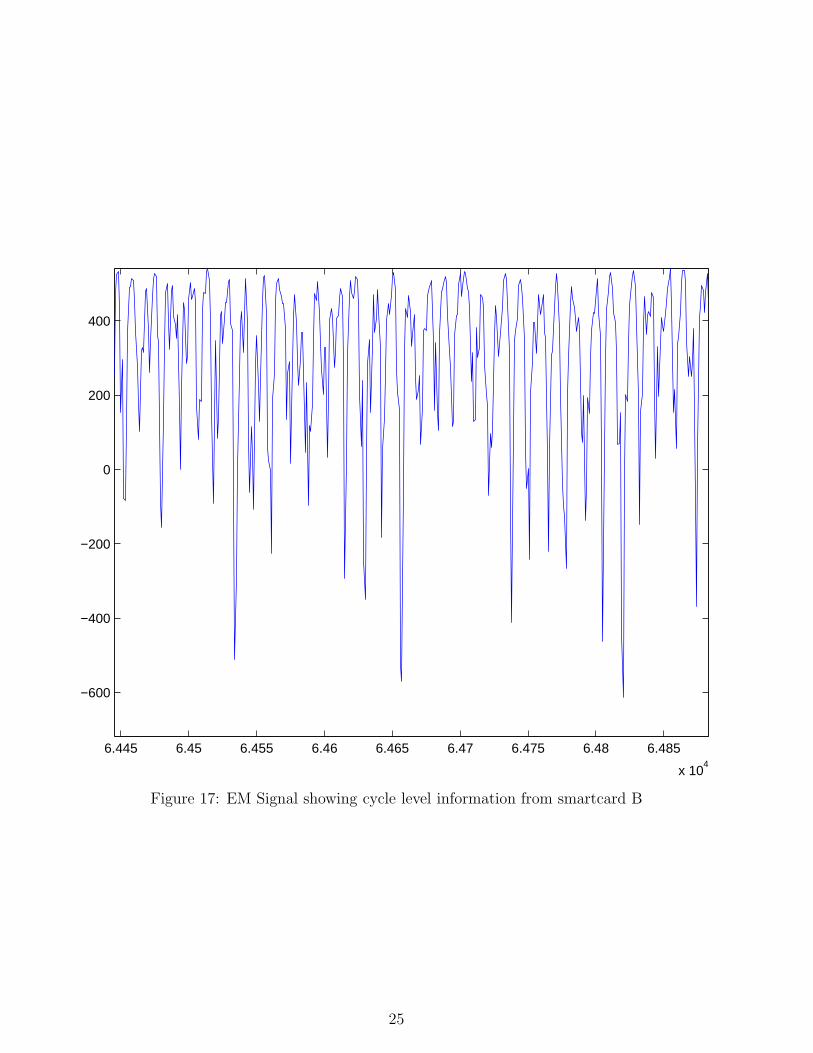
band. Figures 3.1.1,3.1.1 and Figure 3.1.1, shows the caputured signal (plotted as amplitude vs timein 10ns units) at different time scales. At a macroscopic level, in Figure 3.1.1 one can see the overallstructure of the computation, i.e, 16 similar sized structures terminated by sharp negative peaks foreach of the 16 rounds of DES. At an intermediate level of resolution, Figure 3.1.1 shows two rounds ofDES. In each round, there are three regions with different densities of negative peaks. These regionscan be contrasted to the regions visible in Figure 13. At a microscopic level, one can see emanationsat the clock cycle level as shown in Figure 3.1.1.
3.1.2 SEMA
In a SEMA attack, an adversary is able to extract compromising information from a single EM sample.If a computation makes use of conditional branches based on secret information, then on a compromis-ing EM signal, this can be observed as relative shifts in the distances between major computationalstructures. In some cases, these shifts may be sufficient to reveal the branch taken, which in turnconfirms the value of the secret information. This is analogous to what has already been demonstratedfor power samples [11]. Thus conditional statements in the code could provide valuable opportunitiesfor both SPA and SEMA.
In our opinion, the interesting case is where SEMA attacks are successful in extracting informationwhereas SPA attacks fail. This is possible if an EM signal for some instruction leaks more informa-tion than the power side-channel. The following experiment which shows the existence of such “badinstructions” confirms this possibility.Bad Instructions:In the following set of figures, we consider smartcard B in which the internal noise generators had beenturned off. In such a setting, we observed that an instruction which tests a bit of a byte in the memoryleaks information about the tested bit from even a single signal sample in the EM side-channel butnot in the power side-channel. Each figure plots the amplitudes of two signals with respect to time (in10ns units).
Figure 18 shows two EM signals in which the bits tested are both 0, In both figures the data wascollected by a 12bit, 100Mhz scope after demodulating at the 262Mhz carrier. This is seen as a lowvalue in both the signals at the point 18915. Figure 19 shows two EM signals in which one of thebits tested is 0 and the other is 1. This is seen as a low value in one of the signals and a high valuein the other at the point of interest which in this case is 18780. The corresponding figures for thepower side-channel are shown in Figures 20 (at point 19260) and 21 (at point 18990) respectively.The power signal levels, at the corresponding points where the EM emanations differed widely, arevery close. This was also verified by taking averages of 1000 power samples. The experiment onceagain confirmed that the averaged signal at the point of interest was almost identical for the 0 and 1bit.
Even with noise enabled, it was possible to classify the bit value correctly with high probabilty byusing only a few samples (20–30). Section 4.2.1 illustrates this with an example. This example alsoshows the value of EM side-channels—this bit value had no easily observable leakage in the powerside-channel and even statistical attacks required several thousand samples.
Since the last four figures were obtained by considering individual samples and a skeptical readermay remain unconvinced, we now present statistical observations over 2000 samples for three cycles ofthe same “bad” bit-test instruction as opposed to the approximately 1.5 cycles illustrated in the lastfour figures.
Figure 22 shows two signals corrresponding to mean EM signals (each taken over 1000 samples)
26

obtained during the execution of a “bad” bit-test instruction when the tested bit was 0 and 1 respec-tively. As can be seen, the mean signals differ significantly at a few places, namely those at which thetested bit influences the EM emanations.
Figure 23 shows two signals corresponding to the standard deviation of the EM signals (each takenover 1000 samples) obtained during the execution of a “bad” bit-test instruction when the testedbit was 0 and 1 respectively. It turns out that while the means and standard deviations of the EMsignals are sufficient to distinguish the tested bit with non-negligible probability (as was shown inSection 4.2.1), the corresponding values for the power signals are not.
3.1.3 DEMA
The analogy for differential power analysis (DPA) is DEMA. DEMA results from 3 different EM signalsare presented in Section 2.3.
3.2 Defeating Power Analysis Countermeasures
In [11], a suggested countermeasure to power analysis is to use only those instructions whose powerleakage is not excessive and to refresh sensitive information, such as a key, after each invocation in anon-linear fashion. This forces the adversary is extract a substantial portion of the key from a singleinvocation since incomplete key information does not help in subsequent invocations. Another class ofcountermeasures based on splitting all sensitive information into shares was proposed in [1, 6]. Thebasic idea here is that uncertainty in the information about each share is exponentially magnified inproportion to the number of shares. The key to breaking both classes of countermeasures is to identify“bad” instructions which leak much more information in some EM side-channels than the traditionalside-channels. Such instructions if used in power-analysis resistant implementations would subvert thevery assumptions supporting their resistance. Similarly, excessive leakage in intstructions dealing withshares would diminish the very uncertainity being magnified by the shares leading to a compromise ofsensitive information.
For all chip cards that we examined, there were several such instructions. In our investigations,we did not find any instruction that leaked in the power side-channel but did not leak in some EMside-channel. This can happen if all critical parts of a chipcard are well-shielded but the power signalis not. We feel that this is unlikely since a designer who shields EM emanations so well is also likely
1.889 1.8895 1.89 1.8905 1.891 1.8915 1.892 1.8925 1.893 1.8935 1.894
x 104
−600
−500
−400
−300
−200
−100
0
100
200
300
Figure 18: Two EM Signals where tested bits are 0 (seen as low values at 18915)
27

1.876 1.8765 1.877 1.8775 1.878 1.8785 1.879 1.8795 1.88
x 104
−500
−400
−300
−200
−100
0
100
200
300
Figure 19: Two EM Signals where tested bits are 0 and 1 (seen as low and high values at 18780)
1.922 1.923 1.924 1.925 1.926 1.927 1.928 1.929 1.93
x 104
−600
−400
−200
0
200
400
600
800
1000
Figure 20: Two Power Signals where tested bits are 0 at 19260
1.895 1.896 1.897 1.898 1.899 1.9
x 104
−800
−600
−400
−200
0
200
400
600
Figure 21: Two Power Signals where tested bits are 0 and 1 at 18990
28

0 10 20 30 40 50 60 70 80 90 100−50
−40
−30
−20
−10
0
10
20
Figure 22: Mean signals over 3 cycles for a bad instruction where the computation differs only in onebit
0 10 20 30 40 50 60 70 80 90 1000
50
100
150
200
250
300
Figure 23: Standard deviations of signals over 3 cycles for a bad instruction where the computationdiffers only in one bit
to protect against power signal leakages. In the absence of shielding, we believe that a power signalleakage implies leakage in EM emanations due to the physics of the semiconductor devices.
The bit test instruction is a very useful instruction for implementing algorithms, such as DES, whichinvolve bit level permutations. For example, it can be used for key expansion and P-permutation.Based on its low leakage characteristics in power, there is no reason for not using such a usefulinstruction in power analysis resistant implementations. If this instruction is used for this purposeon this card with noise disabled, then a SEMA attack would be sufficient to extract the DES keyregardless of which class of countermeasures [11, 1, 6] was used. However, if noise was enabled, thenthe countermeasure of [11] may still work while feasible higher order statistical attacks would stilldefeat the countermeasures of [1, 6].
3.3 Higher Order EM Attacks on Secret-Sharing
DPA countermeasures based on secret-sharing schemes choose an appropriate value for the numberof shares based on the leakage characteristics and the desired level of resistance against higher orderpower analysis [11], in terms of the number of samples required to break the implementation. If aleakage is superior in an EM signal, then the number of samples for the corresponding higher order
29

EM attack will be substantially lower.To verify this, we implemented a two-way XOR-based secret sharing scheme for bits on the chipcard
where the bit test instruction (described in the previous section) leaks more information on an EMsignal. This sample code split the input bits into pairs of shares and tested the values of the bits ofthe shares using the bit test instruction. We confirmed that DPA and DEMA did not work, i.e., nosingle point in the power/EM signal correlated with any of the input bits. We then performed a secondorder DEMA attack using 500 EM signals. Specifically, we defined a statistical measure on the signalat two points where the two shares of a bit were being tested. We observed a significant difference inthe measure for the case where a zero bit was shared as opposed to where a one bit was shared. Nosuch difference was observed with five thousand power samples. We illustrate these results in the nextsection which deals with a more general case.
A valid criticism of the above experiment is that we had the benefit of knowing exactly wherethe shares were being manipulated and also the bad instructions being used. In real life, it is highlyunlikely that an adversary would have any knowledge of code in the card. Thus the attack will onlybe useful in practice if it can deal with unknown code.
3.3.1 Attacks on Unknown Code
Suppose we are given a chipcard containing an unknown k-way secret-sharing based DPA protectedcode for a known algorithm. Further assume that “bad” instructions have already been identified andsome of these instructions are used to manipulate shares. These, of course, are necessary conditionsfor EM attacks to be more effective than power attacks. Let us also assume that it is also possibleusing signal processing to remove execution sequence and variable clock randomization that has beenadded as countermeasures to complicate alignment of signals and each signal can be realinged into acannonical execution sequence14
The value of k is usually small. For simplicity, assume that k is 2: the attack generalizes for slightlylarger k. Fix a reasonable limit L on the number of EM samples that can be collected. We now showthat if k is small and if with knowledge of the code we could have broken the protected code using Lsamples, then this attack can break the unknown protected code with O(L) samples.
In case of a two-way split, a first step is to identify the two locations where the shares of algo-rithmic quantity are being manipulated using bad instructions in the computation. If code-executionrandomization can be removed using signal processing, then this can, in principle be done for manyalgorithms. Knowing the algorithm, one can provide two different inputs such that the value of thevariable is different for these inputs while most of the other variables are the same within the windowof interest. For example, in DES one could choose two inputs which differ only on chosen 1 bit, sothat only the output of a single S-box is affected. This way we can try to discover where the shares ofthe output of the S-box are manipulated in the cannonical execution sequence.
Take L EM samples for each of these two different inputs. If the exact locations were known thenthere is second order statistic, S, that can be applied to the signal at these two locations to distinguishbetween the two different inputs, thus enabling hypothesis testing.
Without location information, one can only assume that the two locations are an integral number,D, of clock cycles apart. So the strategy is to compute the statistic S for each point on the signalwith respect to a corresponding point D cycles away. This exercise is done for both sets of inputs forall reasonable values of D. If the shares of the variable are not manipulated at distance D, then the
14In our experience this has been quite feasible, especially since one does not need perfect canonical realignment, onlyan alignment which is correct with a reasonable probability.
30

0 0.5 1 1.5 2 2.5
x 104
−1
−0.8
−0.6
−0.4
−0.2
0
0.2
0.4
Figure 24: Difference in correlation statistics for D = 40, L = 500
values of the statistic S at all points will be similar for the two inputs. However, for the right value ofD, there will be a significant difference in S exactly at the point where the first share is manipulatedand thus the exact location of each share is revealed.
A practical optimization is to choose the two inputs so that multiple variables are different. Thenthe above exercise will yield candidate locations for the shares for these variables. Once share locationsare identified, second (or higher) order attacks can be applied as if the code were known.
We illustrate this attack on the test implementation with the bit test instruction mentioned earlier.In the implementation, the shares of one of the input bits were tested 40 cycles apart. Section 3.1shows that when a bit is 1, the signal at the bit test instruction is high and when the bit is 0, thesignal is low. For a 2-way bit split using an XOR-scheme, the shares of a 0 bit will be (0, 0) or (1, 1)with equal probability and the shares of a 1 bit would be (0, 1) or (1, 0) with equal probability. Thissuggests that a good statistic S is the correlation coefficient between the corresponding signal pointswhere the shares of bits are being tested. S will be positive when the bit is 0 and negative when thebit is 1.
0 0.5 1 1.5 2 2.5
x 104
−0.5
−0.4
−0.3
−0.2
−0.1
0
0.1
0.2
0.3
0.4
Figure 25: Difference in correlation statistics for D = 50, L = 500
We experimented with L = 500, for two different inputs, which differed in exactly three bits.Figure 24 shows the difference in the statistic S when the distance D is 40, plotted against elaspedtime in 10ns units. The three significant negative peaks were confirmed to be at exactly the points
31

where the first shares of the three bits (that differ) were being manipulated. No peaks were found whenD differed from 40, e.g, Figure 25 shows the case for D = 50. No peaks were seen even for D = 40 forfive thousand power signals, showing that higher order DPA does not work with five thousand signals.Our findings also show that this EM attack even works with L = 200.
4 Adversarial Model, Attacks and Leakage Assessment
This section develops and uses an adversarial model to formally address issues relating to leakage ofinformation via multiple side-channel signals using several sensors. In particular, we address questionssuch as: Given a limit on signal collection capabilities, which signals should an adversary choose?Can the information obtained by combining leakages from several (or even all possible) signals fromavailable sensors be quantified regardless of the signal processing capabilities and computing powerof an adversary? For reasons explained in the Introduction, this model does not deal with specificalgorithms and implementations. Instead, it focuses solely on the elementary leakages of informationabout relevant states in each cycle of each elementary operation of CMOS devices via sensors todifferent adversaries including unbounded ones.
4.1 Adversarial Model
In CMOS devices, compromising side-channel signals during each clock cycle depend solely15 on therelevant state at the beginning of the cycle and some random thermal noise (see Section 2). It istherefore natural to formulate questions about the information leakage in terms of the relevant state.For example, an adversary may be interested in the LSB of the data bus during a LOAD instruction.This has a natural formulation as a binary hypothesis testing problem for the adversary16. Such aformulation also makes sense as binary hypothesis testing has traditionally been central to the notionsof side-channel attack resistance and leakage immunity defined and used earlier [1, 3].
The adversarial model consists of two phases. The first phase, known as the the emanation profilingphase, is a training phase for the adversary. He is given a training device identical to the target device,an elementary operation, two distinct probability distributions B0 and B1 on the relevant states fromwhich the operation can be invoked and a set of sensors for monitoring side-channel signals. Theadversary can invoke the elementary operation, on the training device, starting from any relevantstate. It is expected that adversary uses this phase to prepare an attack. In the second phase, knownas the hypothesis testing phase, the adversary is given the target device and the same set of sensors.
He is allowed to make a bounded number of invocations to the same elementary operation on thetarget device starting from a relevant state that is drawn independently for each invocation accordingto exactly one of the two distributions B0 or B1. The choice of distribution is unknown to the adversaryand his task is to use the signals on the sensors to select the correct hypothesis (H0 for B0 and H1 forB1) about the distribution used. The utility of the side-channel can then be measured in terms of thesuccess probability the adversary can achieve as a function of the number of invocations allowed.
15In practice, this is a very good first approximation. Minor deviations due to residual second order effects can alsobe addressed as they are transient.
16In general, the adversary faces an M -ary hypothesis testing problem on functions of relevant state, for which resultsare straightforward generalizations of binary hypothesis testing.
32

4.2 Sophisticated Adversarial Strategies
Hypothesis testing is a well researched area in fields such as Information Theory, Statistics and SignalDetection Theory. Techniques from these areas provide several sophisticated strategies that even anadversary with limited resources can use. We now describe one such technique which is optimal intheory, but may require some assumptions and approximations to implement in practice.
In the emanation profiling phase, the adversary builds a statistical profile of the signals availablefrom sensors for each hypothesis H0 and H1. For each hypothesis, the adversary performs K indepen-dent experiments in which the relevant state is drawn according to distributions B0 and B1. In eachexperiment, he collects a vector O of n signals (i.e., O = [O1, . . . , On]
T ) from the sensors. 17.As a result, for each hypothesis, he obtains a collection, Oi = [Oi1, . . . , Oin]T , i = 1, . . . , K, of
signal vectors. He then computes the average sensor signal denoted by S = S1, . . . , Sn, whereSj =
∑Ki=1 Oij/K. Subtracting the average sensor signal S from the observation vectors O1, . . . ,OK ,
produces K noise signal vectors N1, . . . ,NK. The next step is to derive the statistical characterizationof the noise signal under this hypothesis using N1, . . . ,NK as samples. It is well known that if the valueof K is large enough, a complete statistical characterization of the noise signals in form of a probabilitydensity function pN(·) can be obtained at least in theory [5]. The results of the emanation profilingphase are the signal characterizations, S0 and S1, and the noise probability density characterizations,pN0(·) and pN1(·) for the two hypotheses.
In the hypothesis testing phase. the adversary acquires L sets of sensor signals Oi, i = 1, . . . , L.It is well-known that in order to minimize the probability of error in hypothesis testing, the adver-sary should conduct the maximum likelihood test. The likelihood ratio Λ(O1, . . . ,OL) is given by∏L
i=1 pN1(Oi − S1)/pN0(Oi − S0). The adversary decides in favor of H1 if Λ(O1, . . . ,OL) > 1, anddecide in favor of H0 otherwise.
While the approach thus far is optimal, it may be impractical as an exact characterization of thenoise probability density pN(·) may be infeasible. Such a characterization has to capture the natureof each of the noise signals and the dependencies between them. This could further be complicatedby the fact that, in addition to thermal noise, the noise signals could also display additional structuredue to the interplay between properties of the device and those of the distributions. For example, ifthe hypothesis was on the LSB of a register while the device produced widely different signals onlywhen the MSB was different, the noise signals will display a bimodal effect attributable to the MSB.Noise characterization, however is a well studied problem, and there exist a rich set of techniqueswhich allow one to obtain near optimal results by making the right assumptions about the noise. Suchassumptions greatly simplify the task by permitting the use of only partial characterizations of noise.
4.2.1 The Gaussian Assumption
One widely applicable assumption is the Gaussian assumption which states that the noise vector N hasa multivariate Gaussian distribution with zero mean and a covariance matrix ΣN . Such an assumptionapproximately holds for a large number of devices and hypotheses encountered in practice. Use ofsuch multivariate statistics provides far better results, such as greatly reduced error probabilitiesfor hypothesis testing, as compared to current side channel attack techniques. Such modeling alsopermits comparison of different multiple signal selection strategies. This analysis often results incounterintuitive multi-signal selection strategies: e.g., sometimes it is better to use signals with low
17Practical issues regarding the composition of these signals and the value of n will be described later.
33

signal-to-noise ratio and low noise correlation than signals with high signal-to-noise ratio but highnoise correlation.
Figure 26 illustrates the noise distribution at a single point in the execution of the “bad” instructionshown in Figures 22 and 23. As can be seen the noise distribution is well approximated by a Gaussiandistribution. It should be noted that sometimes a better approximation to the noise density is beobtained by a mixture of Gaussian densities. In other cases, analysis based on such an assumption isstill useful as it provides valuable insights and often, improvements by more refined models may not besignificant. We also mention that there is a significant body of techniques dealing with non-Gaussiannoise, whose description is beyond the scope of this paper.
−800 −600 −400 −200 0 200 400 6000
10
20
30
40
50
60
70
80
90
Figure 26: Noise distribution of an EM signal at a single point (point 5 in 3 cycles for a bad instruction)showing an approximately Gaussian distribution
A multivariate Gaussian distribution pN(·) has the following form:
pN(n) =1√
(2π)n|ΣN |exp(−1
2nT Σ−1
N n), n∈Rn (1)
where |Σn| denotes the determinant of ΣN and Σ−1N denotes the inverse of ΣN . For simplicity, we
assume that the noise densities for the two hypotheses, pN0(n) and pN1(n) are the same and denotedby pN(n). With these assumptions, the hypothesis test based on the likelihood ratio for a singleobservation18 simplifies to: The adversary decides in favor of H1 if (S1 − S0)
T Σ−1N O τ , and in
favor of H0 otherwise, where τ = 12(ST
1 Σ−1N S1 − ST
0 Σ−1N S0) (see [14]). Note that under the Gaussian
assumption, only the covariance matrix ΣN needs to be determined for maximum likelihood testing.The following well-known result from the Detection Theory is now applicable [14].
Fact 1 For equally likely binary hypotheses, the probability of error in maximum likelihood test isgiven by
Pε =1
2erfc
( ∆
2√
2
)(2)
where ∆2 = (S1 − S0)T Σ−1
N (S1 − S0) and erfc(x) = 1 − erf(x). Note that ∆2 has a nice interpretationas the optimal signal-to-noise ratio that an adversary can achieve under the Gaussian assumption.
18Generalizations to multiple observations are straightforward.
34

Example 1 To show the power of maximum-likelihood testing, consider a chipcard with a “bad” in-struction, such as the one described in Section 3. EM signals and their statistics for such an instructionare shown in Figures 22 and 23 respectively in Section 3.1.2. It is clear from the Figure 22 that themaximum difference in the mean signals occurs at point 5. A simple approach to binary hypothesistesting would be to compare a given observation to the mean signals at this point and decide in favorof the mean signal which is closer to the observation. In an experiment consisting of 2000 such obser-vations, this approach results in a probability of error of 49.7% which is marginally better than justguessing.
Clearly, the probability of error can be reduced by considering all the points in the observation. Asimple approach again is to compute the Euclidean distance between the observation and the meansignals and decide in favor of the closer signal. In an experiment consisting of 2000 such observations,this approach results in a probability of error of 48.8% which is somewhat better than using just onepoint. However, for the maximum likelihood testing, the probability of error for the same observationsturns out to be 44.7%. This is in excellent agreement with the probability of error of 45.5% predictedby (2). This agreement validates our Gaussian assumption for this particular instruction and thechipcard.
It should be kept in mind that we have achieved this bias just by looking at one bit in oneinvocation of a “bad” instruction. It can be shown that the error probability for maximum likelihoodtesting decreases exponentially in the number of invocations. This implies that the error probabilitycan be made arbitrarily small with only a modest increase in the number of invocations, say, 20–30.
Since erfc(·) decreases exponentially with ∆, the goal of a resource-limited adversary would be tochoose signals in such a manner, as to maximize the output signal-to-noise ratio ∆2. As shown below,this goal differs from the naive approach of choosing the signals with best signal-to-noise ratios andthen feeding them into a signal processing unit to test a hypothesis.
Example 2 Consider the case where an adversary can collect two signals [O1, O2]T at a single point
in time, such that under the hypothesis H0, Ok = Nk, for k = 1, 2, and under the hypothesis H1,Ok = Sk + Nk. Assume that N = (N1, N2)
T has zero mean multivariate Gaussian distribution with
ΣN =
(1 ρρ 1
)
Note that O1 and O2 have signal-to-noise ratios of S21 and S2
2 respectively. After some algebraicmanipulations, we get
∆2 =(S1 + S2)
2
2(1 + ρ)+
(S1 − S2)2
2(1 − ρ)(3)
Now, consider the case of an adversary who discovers two AM modulated carrier frequencies whichare close and carry compromising information, both of which have very high and equally good signal-to-noise ratios (S1 = S2) and another AM modulated carrier in a very different band with a lowersignal-to-noise ratio. An intuitive approach would be to pick the two carriers with high signal-to-noiseratio. In this case S1 = S2 and we get, ∆2 = 2S2
1/(1 + ρ). Since both signals originate from carriers ofsimilar frequencies, the noise that they carry will have a high correlation coefficient ρ, which reduces∆2 at the output. On the other hand, if the adversary collects one signal from a good carrier and theother from the worse quality carrier in the different band, then the noise correlation is likely to belower or even 0. In this case:
∆2 =(S1 + S2)
2
2+
(S1 − S2)2
2= S2
1(1 + S22/S
21) (4)
35
It is clear that the combination of a high and a low signal-to-noise ratio signals would be a betterstrategy as long as S2
2/S21 > (1 − ρ)/(1 + ρ). For example, if ρ > 1/3, then choosing carriers from
different frequency bands with even half the signal-to-noise ratio results in better hypothesis testing.
Results obtained by using the Gaussian assumption are useful in analyzing several situations. Forinstance, suppose we have only analyzed the signal-to-noise ratios of two channels and not the noisecorrelations between them. Suppose an adversary collects a signal from each of these channels byinvoking an operation. We can still compute a lower bound on his error probability by assuming thatρ = 0, since his error probability will only increase as the correlation coefficient ρ increases. In general,even for non-Gaussian noise distributions, a lower bound on the error probability can be obtained byassuming that multiple sets of sensor signals are statistically independent.
4.3 Leakage Assessment Methodology for Chipcards
Maximum likelihood testing is the optimal way to perform hypothesis testing. Thus, we use it to crafta methodology to assess information leakage from elementary operations. Our methodology takes intoaccount signals extractable from all the given sensors across the entire EM spectrum. Results of suchan assessment will enable one to bound the success probability of the optimal adversary for any givenhypothesis.
Assume, that for a single invocation, the adversary captures the emanations across the entireelectromagnetic spectrum from all sensors in an observation vector O. Let Ω denote the space of allpossible observation vectors O. Since the likelihood ratio, Λ(O) is a function of the random vector O,the best achievable success probability, Ps, is given by:
Ps =∑O∈Ω
IΛ(O)>1pN1(O − S1) + IΛ(O)<1pN0(O − S0) (5)
where IA denotes the indicator function of the set A.When the adversary has access to multiple invocations, an easier way of estimating the probability
of success/error involves a technique based on moment generating functions. We begin by defining thelogarithm of the moment generating function of the likelihood ratio:
µ(s) = ln( ∑
O∈Ω
psN1(O − S1)p
1−sN0 (O − S0)
)(6)
The following is a well-known result from Information Theory:
Fact 2 Assume we have several statistically independent observation vectors19 O1,O2, . . . ,OL. Forthis case, the best possible exponent in the probability of error is given by the Chernoff Information:
Cdef= − min
0s1µ(s)
def= − µ(sm) (7)
Note that µ(·) is a smooth, infinitely differentiable, convex function and therefore it is possible toapproximate sm by interpolating in the domain of interest and finding the minima. Furthermore,under certain mild conditions on the parameters, the error probability can be approximated by:
Pε ≈ 1√8πLµ′′(sm)sm(1 − sm)
exp(Lµ(sm)) (8)
19For simplicity, this paper deals with independent elementary operation invocations. Techniques also exist for adaptiveinvocations.
36

Note that in order to evaluate (5) or (8), we need to estimate pN0(·) and pN1(·). In general, this canbe a difficult task. However by exploiting certain characteristics of the CMOS devices, estimation ofpN0(·) and pN1(·) can be made more tractable.
4.4 Practical Considerations
We will now outline some of the practical issues associated with estimating pN0(·) and pN1(·) forany hypothesis. The key here is to estimate the noise distribution for each cycle of each elementaryoperation and for each relevant state R that the operation can be invoked with. This results in thesignal characterization, SR, and the noise distribution, pNR(·) which is sufficient (see Theorem 1) forevaluating pN0(·) and pN1(·).
There are two crucial assumptions that facilitate estimating pNR(·): first, on chipcards examined byus the typical clock cycle is 270 nanoseconds. For such devices, most of the compromising emanationsare well below 1 GHz which can be captured by sampling the signals at a Nyquist rate of 2 GHz. Thissampling rate results in a vector of 540 points per cycle per sensor. Alternatively, one can also captureall compromising emanations by sampling judiciously chosen and slightly overlapping bands of theEM spectrum. The choice of selected bands is dictated by considerations such as signal strength andlimitations of the available equipment. Note that the slight overlapping of EM bands would result ina corresponding increase in the number of samples per clock cycle, however it remains in the range of600-800 samples per sensor.
The second assumption, borne out in practice, is that for a fixed relevant state, the noise distributionpNR(·) can be approximated by a Gaussian distribution. In Section 4.2.1, we provide experimentalevidence to validate this assumption for CMOS devices. This fact greatly simplifies the estimation ofpNR(·) as only about one thousand samples are needed to roughly characterize pNR(·). Moreover, thenoise density can be stored compactly in terms of the parameters of the Gaussian distribution.
These two assumptions imply that in order to estimate pNR(·) for a fixed relevant state R, weneed to repeatedly invoke (say 1000 times) an operation on the device starting in the state R, andcollect samples of the emanations as described above. Subsequently, the signal characterization SR
can be obtained by averaging the collected samples. The noise characterization is obtained by firstsubtracting SR from each of the samples and then using the Gaussian assumption to estimate theparameters of the noise distribution.
The assessment can now be used to bound the success of any hypothesis testing attack in ouradversarial model. For any two given distributions B0 and B1 on the relevant states, the correspondingsignal and noise characterizations, S0, S1, pN0(·), and pN1(·), are a weighted sum of the signal and noiseassessments of the constituent relevant states SR and pNR(·). The error probability of maximum-likelihood testing for a single invocation or its exponent for L invocations can then be bounded using(5) and (7) respectively.
We now give a rough estimate of the effort required to obtain the leakage assessment of an el-ementary operation. The biggest constraint in this process is the time required to collect samplesfrom approximately one thousand invocations for each relevant state of the elementary operation. Foran r-bit machine, the relevant states of interest are approximately 22r; thus the leakage assessmentrequires time to perform approximately 1000 ∗ 22r invocations. Assuming that the noise is Gaussianand that each sensor produces an observation vector of length 800, for n sensors the covariance matrixΣN has (800 ∗ n)2 entries. It follows that the computation burden of estimating the noise distributionwould be proportional to (800 ∗ n)2. Such an approach is certainly feasible for an evaluation agency,from both a physical and computational viewpoint, as long as the size of the relevant state, r, is small.
37

In our experiments, we found such assessment possible for a variety of 8-bit chipcards.
4.5 Completeness Theorem for Elementary Leakages
Finally, we conclude this paper with a theorem to justify the completeness of our assessment processfor gauging side-channel vulnerabilities not just at a cycle level but vulnerabilities of entire implemen-tations.
Our model and vulnerability assessment deals with the leakage of information about the relevantstate of elementary operations at the cycle level. Thus it can directly be used to assess cycle bycycle leakage of relevant state information from the side-channels for an implementation, where thecycles are treated independently. This is the case for the classical differential side-channel attacks alsoknown as first-order attacks. However, any implementation which consists of multiple operations willhave very strong dependencies between the relevant states that occur across multiple cycles spreadthroughout the computation. These dependencies are the basis of higher-order differential side-channelattacks like the ones we describe in the paper. Thus, as specified in [1], assessing vulnerabilities forsuch implementations can be modeled as a hypothesis testing exercise to distinguish between twopossible joint distributions of the relevant states in the computation, using the joint signal distributionsintroduced in the side-channel.
On the surface, it may seem that the proposed assessment of vulnerabilities, which takes intoaccount only the cycle by cycle information available from sensor signals about the relevant state, maynot be comprehensive. In this section, we prove a completeness theorem (Theorem 1) that shows thatthis is not the case, i.e., collecting cycle by cycle information about the relevant states is sufficient forthe assessment of vulnerabilities of entire implementations.
Theorem 1 (Completeness of Elementary Leakages) Let H be a hypothesis on the relevantstate distribution of an entire implementation. Let O be any observation vector for the implementationand T (O) be the cycle-by-cycle sufficient statistics obtained using O and our assessment. Then,
I(H ;O) = I(H ; T (O))
That is, all information for hypothesis testing of implementations is in the elementary leakages.
Our proof makes heavy use of information theoretic arguments, and we refer the reader to Coverand Thomas [4] for the background material used here from Information Theory.
Let R = [R1, . . . ,RK]T denote relevant states during an attack that lasts K cycles. Assume thatR is distributed according to a density in the family of probability density functions ph(·) indexedby h∈Ω. The set Ω consists of different hypotheses under test. Let O = [O1, . . . ,OK ]T be the vectorof observations during the attack. As discussed earlier, due to the CMOS circuitry, observations ineach clock cycle depend only on the relevant state in that clock cycle. Mathematically, this can beexpressed by saying that the conditional distribution of Oi depends only on Ri and is conditionallyindependent of the hypothesis h, that is,
Pr(Oi|R) = Pr(Oi|Ri), and (9)
Pr(Oi, h|Ri) = Pr(Oi|Ri)Pr(h|Ri). (10)
Using (9) and (10), it is easy to check that given R, the observations O and the hypothesis h arestatistically independent:
Pr(O, h|R) = Pr(O|R)Pr(h|R) (11)
38
Let T (Oi) be a sufficient statistic for Ri derived from Oi, that is,
I(Ri;Oi) = I(Ri; T (Oi)) for all distributions on Ri. (12)
Here I(X; Y ) denotes the mutual information between X and Y [4]. Let T (O) denote the cycle-by-cycle sufficient statistics given by T (O) = [T (O1), . . . , T (OK)]T . The following theorem asserts that asfar as the determination of hypothesis h is concerned, the information contained in the cycle-by-cyclesufficient statistics is the same as the information contained in the whole observation vector O.
Theorem 2 For the setup described above, regardless of the statistical distribution of hypothesis h,the mutual information between h and O is equal to the mutual information between h and T (O):
I(h;O) = I(h; T (O)) (13)
Proof. Recall that T (Oi) is a sufficient statistics for Ri derived from Oi, that is,
I(Ri;Oi) = I(Ri; T (Oi)) for all distributions on Ri. (14)
Since the conditional distribution of Oi only depends on Ri, by using the chain rule of mutual entropies,we can show that I(R;O) =
∑Kj=1 I(Ri;Oi) and I(R; T (O)) =
∑Kj=1 I(Ri; T (Oi)). As a result
I(R;O) = I(R; T (O)) for all distributions on R. (15)
By the chain rule of mutual entropies,
I(R, h;O) = I(h;O) + I(R;O|h) (16)
= I(R;O) + I(h;O|R) (17)
The conditional independence of O and h given R (see (11)), implies that I(h;O|R) = 0, and,
I(h;O) = I(R;O) − I(R;O|h). (18)
Since T (O) is a function of O, the conditional independence of O and h given R also implies theconditional independence of T (O) and H given R. Using this fact and the chain rule of mutualentropies we can deduce that
I(h; T (O)) = I(R; T (O)) − I(R; T (O)|h). (19)
An examination of (13), (15), (18), and (19) shows that it suffices to prove
I(R;O|h) = I(R; T (O)|h) (20)
Intuitively, the above equality holds since the value of h only determines the distribution of R, and(15) holds regardless of the distribution of R. In the rest of this proof, we will formally show that (20)holds.
We start by expanding I(R,O) for the case when R is distributed according to pω(·) for someω ∈Ω.
I(R,O) = −∑O
p(O) log p(O) +∑O,R
p(R,O) log p(O|R)
= −∑O
(∑R
p(O|R)pω(R))
log(∑
Rp(O|R)pω(R)
)+
∑O,R
p(O|R)pω(R) log p(O|R)
= Hω(O) − Hω(O|R) for all h∈Ω (21)
39

Here Hω(·) denotes the entropy when the distribution of R is given by pω(R). Using a similar argument,we can deduce that
I(R, T (O)) = Hω(T (O)) − Hω(T (O)|R) for all ω ∈Ω
Since I(R,O) = I(R, T (O)) for all distribution of R, it follows that
Hω(O) − Hω(O|R) = Hω(T (O)) − Hω(T (O)|R) for all ω ∈Ω (22)
The following calculation shows that in fact, Hω(O|R) = H(O|R, h = ω) for all ω ∈Ω.
H(O|R, h = ω) = −∑O,R
p(O,R|h = ω) log p(O|R, h = ω)
= −∑O,R
p(R|h = ω)p(O|R) log p(O|R)
= −∑O,R
pω(R)p(O|R) log p(O|R)
= Hω(O|R)
(23)
A similar calculation shows that Hω(T (O)|R) = H(T (O)|R, h = ω), Hω(O) = H(O|h = ω),Hω(T (O)) = H(T (O)|h = ω) for all ω ∈Ω. We can now finish the proof as follows
I(R;O|h) = H(O|h) − H(O|R, h)
=∑ω ∈Ω
p(h = ω)(H(O|h = ω) − H(O|R, h = ω)
)
=∑ω ∈Ω
p(h = ω)(Hω(O) − Hω(O|R)
)
=∑ω ∈Ω
p(h = ω)(Hω(T (O)) − Hω(T (O)|R)
)(24)
=∑ω ∈Ω
p(h = ω)(H(T (O)|h = ω) − H(T (O)|R, h = ω)
)
= H(T (O)|h) − H(T (O)|R, h)
= I(R; T (O)|h)
where (24) follows from (22).
5 Countermeasures
Due to the presence of several unexpected EM leakages, a comprehensive EM vulnerability assessmenthas to be an integral part of any effort to develop countermeasures against EM attacks on specificimplementations. Such countermeasures fall into two broad categories: signal strength reduction andsignal information reduction. Techniques for signal strength reduction include circuit redesign toreduce egregious unintentional emanations and the use of shielding and physically secured zones to
40
reduce the strength of compromising signals available to an adversary relative to ambient thermalnoise. Techniques for signal information reduction rely on the use of randomization and/or frequentkey refreshing within the computation [10, 11, 1, 6] so as to substantially reduce the effectiveness ofstatistical attacks using the available signals.
6 Acknowledgments
We owe a debt of gratitude to Helmut Scherzer for key components that enabled us to explore EMattacks further, in particular, help with the experimental setup, data collection and analysis tools andwith smart card programming. This work has benefited greatly from interactions with EmmanuelYashchin for his suggestions on the use of various statistics and statistical tools. Last but not theleast, we would like to thank Elaine and Charles Palmer for several useful comments and their constantencouragement.
References
[1] Suresh Chari, Charanjit S. Jutla, Josyula R. Rao and Pankaj Rohatgi. Towards Sound Coun-termeasures to Counteract Power–Analysis Attacks. Advances in Cryptology — Proceedings ofCrypto ’99, Springer–Verlag, LNCS 1666, August 1999, pages 398–412.
[2] S. Chari, J. R. Rao and P. Rohatgi. Template Attacks, To appear in Proceedings of CHES ’02.
[3] Jean–Sebastien Coron, Paul Kocher and David Naccache. Statistics and Secret Leakage. In theProceedings of Financial Cryptography ’00. Lecture Notes In Computer Science, Springer–Verlag,2000.
[4] T.M. Cover and J. A. Thomas. Elements of Information Theory. John WIley & Sons Inc, 1991.
[5] H. Cramer. Mathematical Models of Statistics. Princeton University Press. 1946.
[6] L. Goubin and J. Patarin. DES and Differential Power Analysis. Proceedings of the Workshop onCryptographic Hardware and Embedded Systems, CHES ’99, LNCS 1717, August 12–13, 1999,Worcester, MA, pages 158–172.
[7] NSA Tempest Series http://cryptome.org/#NSA--TS.
[8] Dynamic Sciences International Inc. See http://www.dynamic--sciences.com/r1550.html.
[9] K. Gandolfi, C. Mourtel and F. Olivier. Electromagnetic Attacks: Concrete Results. In the Pro-ceedings of the Workshop on Cryptographic Hardware and Embedded Systems 2001 (CHES 2001),LNCS 2162 Paris, France, May 2001, pp 251–261.
[10] P. Kocher. Timing Attacks on Implementations of Diffie-Hellman, RSA, DSS and Other Systems.Advances in Cryptology-Crypto ’96, Lecture Notes in Computer Science # 1109, pp 104–113.
[11] P. Kocher, J. Jaffe and B. Jun. Differential Power Analysis: Leaking Secrets. Advances in Cryp-tology — Proceedings of Crypto ’99, Springer Verlag, LNCS 1666, pages 388–397. One version ofthe paper is available online at http://www.cryptography.com/dpa/technical/index.html.
41

[12] Jean–Jacques Quisquater and David Samyde. ElectroMagnetic Analysis (EMA): Measures andCounter-Measures for Smart Cards. In Smart Card Programming and Security (E-smart 2001),Cannes, France, LNCS 2140, pp.200-210,September 2001.
[13] The complete unofficial TEMPEST web page. Available athttp://www.eskimo.com/ joelm/tempest.html.
[14] H. L. Van Trees. Detection, Estimation, and Modulation Theory, Part I. John Wiley & Sons. NewYork. 1968.
42