the electronic and optical properties of colloidal lead
TRANSCRIPT

THE ELECTRONIC AND OPTICAL PROPERTIES OF COLLOIDAL LEAD-
SELENIDE SEMICONDUCTOR NANOCRYSTALS
A Dissertation
Presented to the Faculty of the Graduate School
of Cornell University
In Partial Fulfillment of the Requirements for the Degree of
Doctor of Philosophy
by
Jeffrey Matthew Harbold
January 2005

© 2005 Jeffrey Matthew Harbold
THE ELECTRONIC AND OPTICAL PROPERTIES OF COLLOIDAL LEAD-
SELENIDE SEMICONDUCTOR NANOCRYSTALS
Jeffrey Matthew Harbold, Ph. D.
Cornell University 2005
Quantum dots of the IV-VI semiconductors, and specifically lead selenide,
strongly confine both electrons and holes, leading to a dramatic modification
of the bulk semiconductor properties. This dissertation is devoted to the study
of the electronic and optical properties of colloidal lead-selenide nanocrystals
or quantum dots.
We begin by discussing the synthesis and characterization of high-quality
colloidal lead-selenide nanocrystals with a narrow size distribution and well-
passivated surfaces. With diameters between 3 and 8 nanometers, these lead-
selenide quantum dots exhibit size-quantized transitions in the infrared region
of the electromagnetic spectrum and exhibit bright band-edge photo-
luminescence tunable from approximately 1000 to 2000 nanometers. These
properties are extremely promising for applications.
The current theoretical understanding of the electronic states of IV-VI
semiconductor quantum dots is based on envelope function approaches and
tight-binding methods. While successful in explaining many features of the
electronic structure, all current calculations fail to explain the presence of
additional peaks in the optical absorption spectrum of lead-selenide and lead-
sulfide quantum dots. We re-examine the leading explanations for these
unexplained transitions and also consider a new possibility, that of enhanced
electric quadrupole transitions.
In addition, the degeneracy of the lowest optical transition in IV-VI
quantum dots is predicted to split by the intervalley coupling of the 4
equivalent L-valleys in the first Brillouin zone. Low-temperature photo-
luminescence and size-selective photoluminescence experiments reveal, for
the first time, a splitting in the emission spectra of lead-selenide and lead-
sulfide nanocrystals. These observations are consistent with a theoretical
treatment of the splitting of the lowest transition in lead-selenide quantum
dots due to intervalley coupling.
The dynamics of electrons and holes are crucially influenced by quantum
confinement. In the strong confinement limit, a dramatic reduction in the
excited state (or intraband) relaxation rate of carriers is predicted to occur.
With its sparse electronic states and simple energy spectra, lead-selenide
quantum dots represent an ideal material system in which to study the
intraband carrier relaxation. We present the first measurements to directly
time-resolve the intraband relaxation of electrons and holes in lead-selenide
nanocrystals. Prior theories cannot explain the observed picosecond time-scale
intraband relaxation and we discuss several possible explanations.

iii
BIOGRAPHICAL SKETCH
Jeffrey Harbold was born in York, Pennsylvania in 1975 to Larry and Linda
Harbold. Jeffrey first revealed his future scientific aspirations when, after a
classroom demonstration by his second grade teacher Mrs. King, he
announced to his parents, “I love science”. Following high school, Jeffrey
moved to Rochester, New York to attend the Rochester Institute of
Technology from which he earned his B.S. in Physics in 1998. Still loving the
climate in the Northeast, Jeffrey then entered the Ph.D. program in Applied
Physics at Cornell University in Ithaca, New York. He joined the Wise
research group in the summer of 1999 and spent the subsequent years learning
about ultrafast lasers, nonlinear optics, and semiconductor quantum dots.
Having surpassed his tolerance for snow and cold, Jeffrey will trade in his
snow boots for flip-flops in January, 2005 as he pursues career and adventure
on the beaches of Southern California.

iv
To Mom and Dad

v
ACKNOWLEDGEMENTS
First, I thank my advisor Frank Wise for his encouragement and advice. His
hands-on style of management and way of showing me how to “do science”
cannot be understated. I could not have asked for a better mentor and I am
indebted to him. I also thank Roger Loring and Joel Brock for serving on my
special committee.
My work over these past years, has largely been the result of fruitful
collaborations. On the nonlinear glass project (not mentioned elsewhere in this
dissertation), I thank J. Sanghera and I. Aggarwal of the Naval Research
Laboratories, B. Aitken and N. Borrelli of Corning, Inc., and T. Birks and W.
Wadsworth of the University of Bath for providing excellent samples and
participating in many helpful scientific discussion. I am very grateful to K. Du
and T. Krauss at the University of Rochester for their role, from day-one, in
the quantum dot project and also for giving me access to their laboratories on
numerous occasions. I thank K.-S. Cho and C. Murray of the IBM T. J. Watson
Research Center for providing quantum dot samples and all the folks at
Evident Technologies for supporting our quantum dot work both directly and
indirectly.
I am fortunate to have spent my time at Cornell in the company of such
wonderful companions in the Wise group. I thank: Sylvia S., for eagerly giving
me the “keys” to my first laser and for all the wisdom she imparted to me
while rushing to complete her degree; Kale B., for endless scientific
discussions and hours upon hours spent contemplating our current and future
lives over cups of coffee, bottles of Coke, and donuts too numerous to count;
Omer I., for assistance in computer modeling on the tapered fiber project and
vi
for proving that it is possible to build an entire optical setup without using a
single screw; P. Fischer, for his wealth of scientific knowledge, his optimism,
and also the reminders that should we both become disillusioned with work at
some point in the future, we always have our secret get-rich scheme to fall
back on; Yi-Fan C., for his enthusiasm, his sense of humor, and his more
recent role as career counselor; Hyungsik L, for our numerous discussions on
work, careers, the arts, and life; Dave H., for sharing enjoyment of CHEM 794
problem sets with me and for usually trumping any problem that I had in the
lab with something much worse; Stephen C. and Yul H. for their assistance on
the quantum dot work; Jeff M., for Monday Night Football; and in no
particular order Joel B., Alexis W., Lyuba K., Andy C., and Shian Z. in
addition to those listed above, for making the Wise group a stimulating and
fun place to be.
My successes are one testament to the vigilance and hard work of
numerous teachers (formal and informal) of whom I have been blessed to be a
student: M. King, C. Rawlinson, P. Mentzer, R. D. Lehman, T. Frey, T.
DeChristopher, J. Andersen, E. Heilweil, and J. Shortall.
Lastly, I thank my family: Mom, Dad, Dan, grandparents, aunts and
uncles. Without their love and support, I could not have achieved this goal.
And after years of their asking again and again, it is with relief that I finally
can answer, “now I’m done”.
vii
TABLE OF CONTENTS
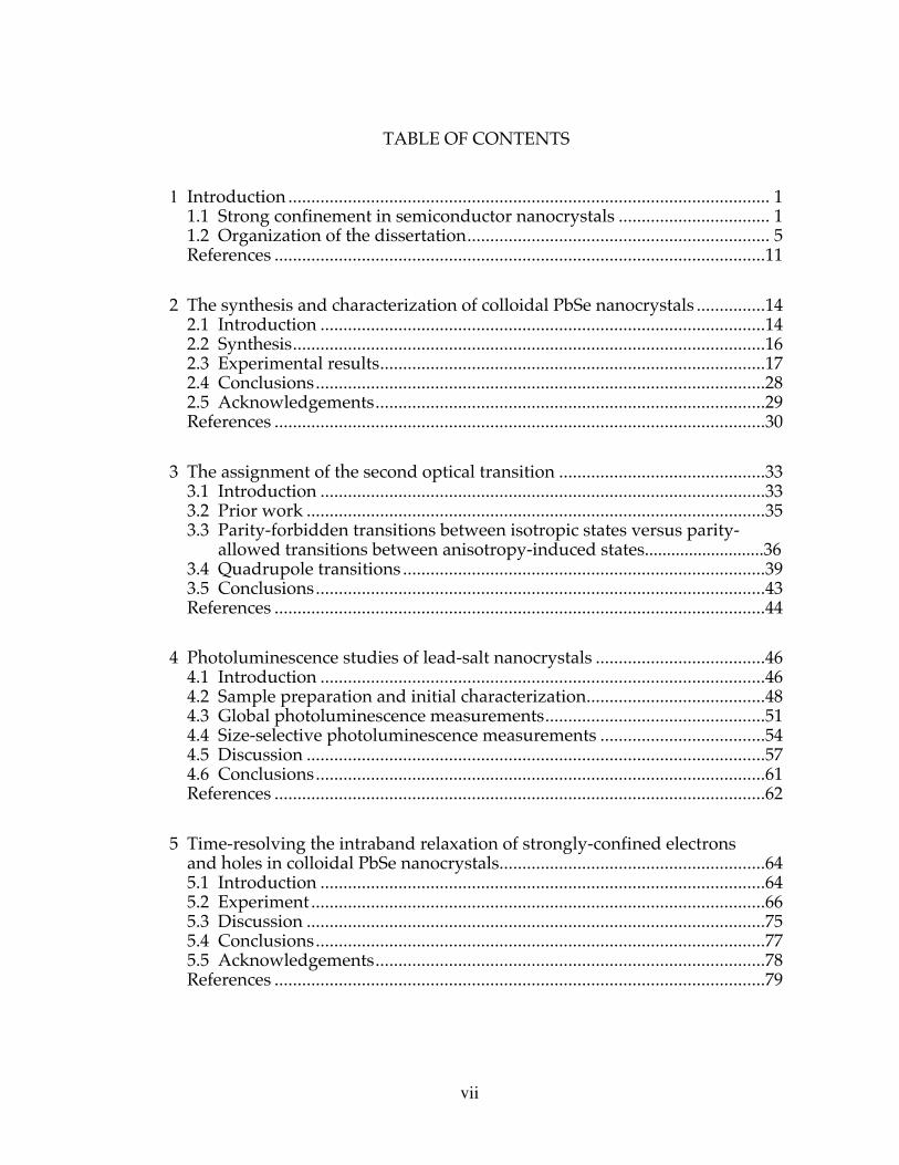
1 Introduction ......................................................................................................... 11.1 Strong confinement in semiconductor nanocrystals ................................. 11.2 Organization of the dissertation.................................................................. 5References ...........................................................................................................11
2 The synthesis and characterization of colloidal PbSe nanocrystals ...............142.1 Introduction .................................................................................................142.2 Synthesis.......................................................................................................162.3 Experimental results....................................................................................172.4 Conclusions..................................................................................................282.5 Acknowledgements.....................................................................................29References ...........................................................................................................30
3 The assignment of the second optical transition .............................................333.1 Introduction .................................................................................................333.2 Prior work ....................................................................................................353.3 Parity-forbidden transitions between isotropic states versus parity- allowed transitions between anisotropy-induced states...........................363.4 Quadrupole transitions ...............................................................................393.5 Conclusions..................................................................................................43References ...........................................................................................................44
4 Photoluminescence studies of lead-salt nanocrystals .....................................464.1 Introduction .................................................................................................464.2 Sample preparation and initial characterization.......................................484.3 Global photoluminescence measurements................................................514.4 Size-selective photoluminescence measurements ....................................544.5 Discussion ....................................................................................................574.6 Conclusions..................................................................................................61References ...........................................................................................................62
5 Time-resolving the intraband relaxation of strongly-confined electrons and holes in colloidal PbSe nanocrystals..........................................................64
5.1 Introduction .................................................................................................645.2 Experiment ...................................................................................................665.3 Discussion ....................................................................................................755.4 Conclusions..................................................................................................775.5 Acknowledgements.....................................................................................78References ...........................................................................................................79

viii
6 Future directions ................................................................................................81References ...........................................................................................................83
7 Appendix ............................................................................................................84Interband transition quadrupole matrix element for lead-salt quantumdots ......................................................................................................................84References ...........................................................................................................89

ix
LIST OF FIGURES
Figure 1.1: The general form of the bulk band structures and the electronicstates that result from the making a QD from (left:) II-VI and III-Vsemiconductors and (right:) IV-VI semiconductors…………………….………..4
Figure 1.2: The general form of the first few electron and hole energy levels ofPbSe or PbS QDs. The states are labeled (right side) by the quantum numbers j(total angular momentum) and p (parity). An alternative scheme (left side)labels the states by the orbital angular momentum of the envelope function.The lowest several dipole-allowed transitions are also depicted……………….6
Figure 1.3: The direct band gap of the IV-VI semiconductors occurs at the 4equivalent L-points of the Brillouin zone………………………………………….8
Figure 2.1: X-ray diffraction pattern of PbSe QDs indexed to the bulk-rock saltcrystal structure. The peaks labeled (*) are due to trace amounts of theunreacted precursor, lead oleate………………………………………………….18
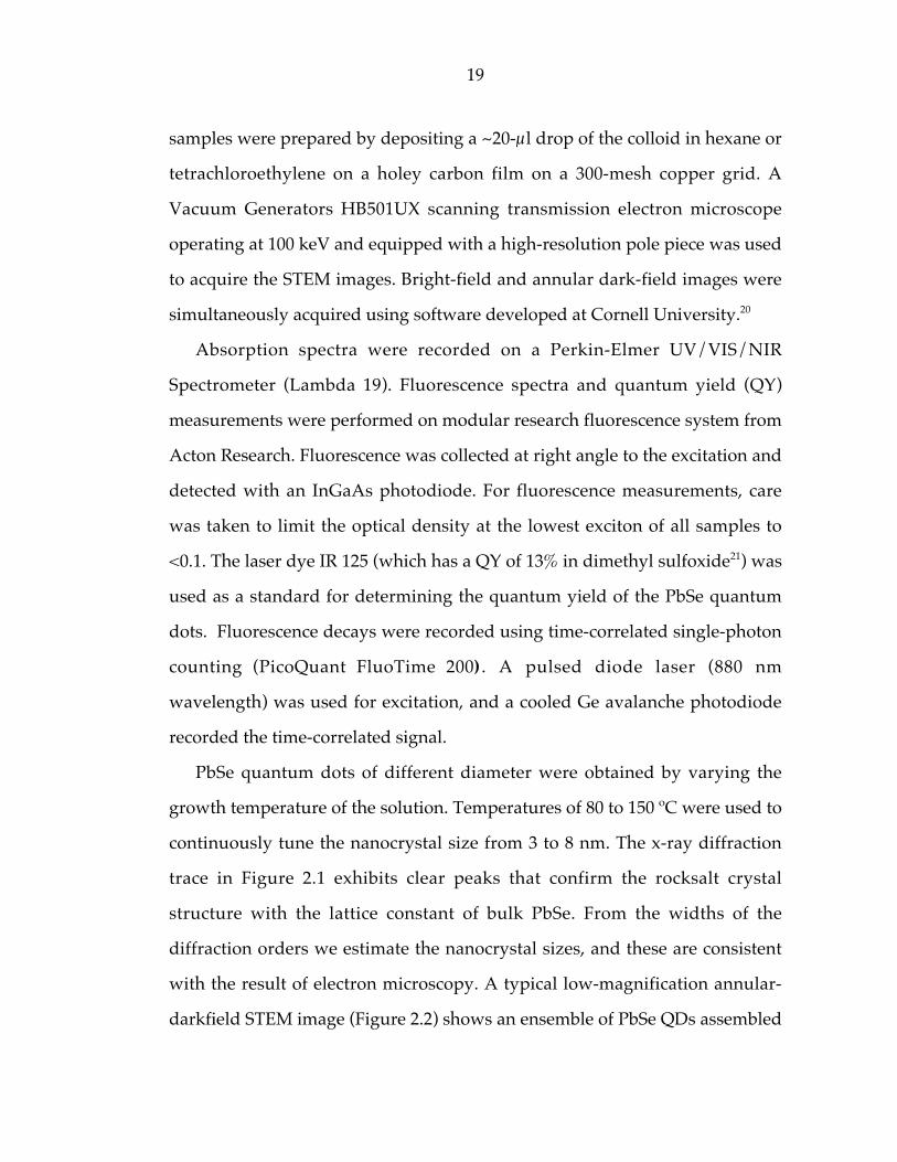
Figure 2.2: Low-resolution STEM micrograph of PbSe QDs (full scale= 320 nm)showing the ordering of an ensemble of NCs…………………………………...20
Figure 2.3: High-resolution STEM micrograph of a PbSe QD (full scale= 6.4nm) revealing lattice imaging of the NC………………………………………....21
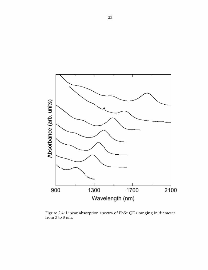
Figure 2.4: Linear absorption spectra of PbSe QDs ranging in diameter from 3to 8 nm……………………………………………………………………………….23
Figure 2.5: Linear absorption spectrum of ~8 nm PbSe QDs with theoreticalcalculations15 of the allowed one-photon transitions (gray bars). The locationof parity-forbidden transitions among the states found by Kang are indicated(dashed arrows) as are the new states arising from the inclusion of theanisotropy of the bulk band structure (solid arrows).22…………………………24
Figure 2.6: Band edge luminescence from PbSe QDs excited at (bottom to top)740 nm, 990 nm, and 990 nm. The measured quantum yields ranged from 12 to81%…………………………………………………………………………………...26

x
Figure 2.7: Luminescence decay for 3-nm PbSe QDs and a single exponentialfit to the data (250-ns time constant). The instrument response to the excitationpulse is much shorter than the measured decay (1.1 ns FWHM)……………...27
Figure 3.1: Room temperature linear absorption spectra of PbSe QDs intetrachloroethylene7 and PbS QDs in glass5. The bars indicate the strength ofthe dipole-allowed transitions calculated in the 4-band envelope functionformalism (normal labels).1 The dashed arrows indicate the predicted energiesof the two lowest dipole-forbidden transitions (italicized labels)……………..34
Figure 3.2: The energy of the several lowest optical transitions in PbSe QDs6, 7,
11 as determined from room-temperature linear absorption spectra. Thescaling of the axes is described in the text. The horizontal lines indicate thepredicted energies of dipole-allowed transitions and dipole forbiddentransitions within the isotropic model1 along with parity-allowed transitionswithin the anisotropic model.2…………………………………………………….37
Figure 4.1: Comparison of the absorption and photoluminescence spectra insolid state film samples to colloidal samples. The solid state film absorptionhas been corrected for scatter by subtracting a 1/l4 background. The peak infilm absorption at ~ 0.9 eV is from oleic acid…………………………………….49
Figure 4.2: The peak of the photoluminescence spectrum shifts to lower energyand narrows with decreasing temperature. The excitation energy is 1.1 eV. Thefeature observed in all of the traces at 0.9 eV is an artifact of the grating…….52
Figure 4.3: Comparison of the low-temperature photoluminescence spectrafrom PbS solid state film and colloidal samples at an excitation energy of 1.27eV. The energy position of the PL structure (~ 0.97 eV and ~ 1.15 eV) does notchange with sample preparation, although the strength of these featuresdoes………………………………………………………………………………......53
Figure 4.4: The intensity dependence of the photoluminescence spectra wasexplored using CW and pulsed excitation. The measured spectra are nearlyidentical despite a difference in peak intensity of approximately 1010. Based onthis observation, we rule out contributions from surface states……………….55
xi
Figure 4.5: Photoluminescence spectra from PbSe QD solid state films at T = 15K. The dashed curves are the measured PL spectra and the solid curves are thebest-fit two-Gaussian decomposition of the measured spectra………………..56
Figure 4.6: Line-narrowed photoluminescence from 4.7-nm PbSe at T = 15 K.The first absorption peak (not shown) is at 0.95 eV. The size-selectiveexcitation is tunable between 0.816 and 0.790 eV. The solid lines labeled withmarkers represent the line-narrowed emission spectra. The solid black like isthe globally-excited PL spectrum and the dashed lines show the best-fit twoGaussian decomposition of the global PL spectrum from Figure 3…………...58
Figure 4.7: The experimentally measured feature splitting for three differentPbSe QD sizes. The splitting is found to increase with both decreasingtemperature and size. We compare these measurements to maximum splittingpredicted in calculations by Allan et al…………………………………………...59
Figure 5.1: The absorption (solid line) and photoluminescence (shaded region)spectra for 6-nm PbSe QDs in the colloidal silica film. The lowest fewelectronic states are calculated using a 4-band envelope function formalism(inset). The strength of the lowest dipole-allowed transitions are indicated byvertical lines. The second absorption feature (italicized label) is discussed inthe text. Separate control measurements of a blank film show that theabsorption peak near 0.6 eV is due to the host…………………………………..67
Figure 5.2: Room-temperature population dynamics of the 1S states, for theindicated densities of photo-excited carriers. The pump pulse is resonant withthe 1Sh - 1Pe transition. The mirror-image 1Se - 1Ph transition is also pumped,but for clarity this is not shown on the energy-level diagram (inset). Theexpanded time scale (right panel) shows carriers entering 1S states. The dottedline is the instrument response……………………………………………………70
Figure 5.3: The population dynamics of the 1Se - 1Sh transition under1Se (h) - 1Ph (e) excitation, for different excitation levels. <Ne-h> is the averagenumber of photo-excited electron-hole pairs per QD. The time at which thepopulation peaks is extracted from a fit to the data (solid lines). The traces arenormalized and then offset for clarity. The delay stage step size was changedat 2 ps, giving the appearance of an abrupt change in noise level……………..71
Figure 5.4: 1P - 1S relaxation time is plotted versus QD diameter…………….73
Figure 5.5: Population dynamics of the 1Se - 1Sh transition with photo-excitedcarrier density for a 2.4-eV pump…………………………………………………74
xii
LIST OF TABLES
Table 1.1: Exciton, electron, and hole Bohr radii of typical semiconductorsused to make colloidal QDs.8…………………………………..…………………3

1
Chapter 1Introduction
1.1 Strong confinement in semiconductor nanocrystals
A nanocrystal (NC) or “quantum dot” (QD) is a small particle of a given
material having the crystal structure of the corresponding bulk material but
exhibiting vastly different electronic properties due to its small size. Quantum
mechanically confining the electrons inside the QD leads to a change in the
electronic states: the effective energy gap increases relative to the bulk
material and discrete exciton states emerge.
The effects of quantum confinement on the electronic states were
investigated theoretically by Efros and Efros.1 They classified the size effects
into three different confinement strength regimes- weak, intermediate, and
strong- by comparing the radius (R) of the QD to the Bohr radius of the
electron (ae) and hole (ah) in the parent bulk medium. The Bohr radii are
defined as
ae ,h =
4π ε(∞)2
me ,h e2 (1.1)
where ε(∞) is the optical frequency dielectric constant, and me,h are the electron
and hole effective masses.
In the case of weak confinement (R > ae, ah), the electron and hole retain
their bulk-like character as an electron-hole pair bound by the Coulomb
interaction (an exciton) and are virtually unaffected by the quantum
confinement. In the intermediate regime (ae > R > ah), the electron is quantized

2
and, as a result, experiences an increase in its energy (confinement energy).
The hole is still unaffected by confinement and remains influenced by the
Coulomb attraction to the confined electron. However, when the confinement
is strong (ae, ah > R), both the energies are significantly increased due to
quantum confinement. In fact, the energy of the strongly-confined charge
carriers is often much greater than the energy of the Coulomb interaction. In
this case, Coulomb effects are typically ignored.
According to Schmitt-Rink et al., the optical properties undergo the
greatest enhancement when the QD radius is smaller than the exciton Bohr
radius, aB
aB =
4π ε(∞)2
e21
me
+1
mh
⎛⎝⎜
⎞⎠⎟
(1.2)
of the bulk semiconductor (aB > R).2 This is based on the observation that as
the dimensionality of the bulk semiconductor is reduced, the density of states
becomes concentrated in narrowing energy bands and eventually discrete
energy states. The effect this narrowing has on the strength of the transitions is
profound; the oscillator strength of a strongly-confined electron-hole pair3
inside a QD is predicted to be a factor of (aB /R)3 times larger than that of the
bulk exciton.2 This implies that quantum dots in the strong confinement limit
have the potential for greatly enhanced optical properties and motivates the
study of semiconductor QDs in this limit.
For other phenomena, such as the excited state relaxation of charge carriers
inside a QD, it is the confinement of the electrons and holes separately that
matters. Little work has been done on QDs that strongly confine both the
electrons and the holes (ae, ah > R). This regime requires either the synthesis of
very small QDs or materials with large electron and hole Bohr radii.

3
Typically, QDs with a radius between 1.5 nm and 8 nm can be fabricated
and attempts to make them smaller results in molecular clusters with a
different crystal structure than the bulk semiconductor.4-7 As shown in Table
1-1, the problem encountered with II-VI and III-V semiconductors is that the
hole Bohr radii are too small; in other words, the holes are too massive.
Therefore, these materials do not allow access to the regime of strong
confinement.
Table 1.1: Exciton, electron, and hole Bohr radii of typical semiconductorsused to make colloidal QDs.8
aB (nm) ae (nm) ah (nm)
II-VI: CdSe 3 3 < 1
II-VI: CdS 2 2 < 1
III-V: InP 9 7 2
III-V: GaAs 10 8 1
IV-VI: PbS 20 10 10
IV-VI: PbSe 47 23 24
In contrast the IV-VI semiconductors, and in particular the lead-salt
compounds, allow easy access to the strong confinement regime. Consider
lead-selenide (PbSe) and lead-sulfide (PbS): the electron and hole masses are
small and nearly identical.8 As shown in Table 1.1, this has the fortunate effect
of leading to large Bohr radii for not only the electron and the exciton but the
hole as well. Strong confinement can then be achieved in relatively large QDs,
with a smaller fraction of their atoms on the surface. The

4
Figure 1.1: The general form of the bulk band structures and theelectronic states that result when making a QD from (left:) II-VI and III-V semiconductors and (right:) IV-VI semiconductors.

5
properties of PbSe and PbS QDs are then far less likely to be influenced by
surfaces effects like surface traps and defects.9
There are other advantages to working with IV-VI semiconductors as
illustrated in Figure 1.1. In II-VI and III-V semiconductors, the confinement
induced coupling between the three (heavy-hole, light-hole, and split-off)
valence bands further complicates the already dense ladder of hole states and
leads to congested energy spectra.10, 11 In contrast, the IV-VI semiconductors
have simple non-degenerate conduction and valence bands. Additionally,
their similarly small electron and hole masses lead to a large and nearly equal
partitioning of the confinement energy between the both charge carriers.
Ultimately, these attributes result in sparse electron and hole states and simple
energy spectra.9
1.2 Organization of the dissertation
This dissertation is devoted to the study of the electronic and optical
properties of colloidal PbSe QDs. In Chapter 2, we discuss the synthesis and
characterization of high-quality colloidal PbSe nanocrystals. Prior to this
work, the best available lead salt nanocrystals were monodisperse and
brightly-emitting PbSe QDs in a glass host.12 The colloidal synthesis presented
here, based on the recent work of Murray and coworkers,13 represents a
significant advancement in the growth of IV-VI NCs with well-controlled size,
a narrow size distribution, and well-passivated surfaces. With diameters
between 3 and 8 nm, these PbSe QDs exhibit size quantized transitions in the
infrared region of the electromagnetic spectrum and exhibit bright band-edge

6
Figure 1.2: The general form of the first few electron and hole energylevels of PbSe or PbS QDs. The states are labeled (right side) by thequantum numbers j (total angular momentum) and π (parity). Analternative scheme (left side) labels the states by the orbital angularmomentum of the envelope function. The lowest several dipole-allowed transitions are also depicted.
7
photoluminescence tunable from approximately 1000 to 2000 nm. These
properties are promising for applications in optoelectronics and microscopy.
In particular, PbSe QDs might enable a broadband and tunable optical
amplifier for telecommunication wavelengths.
As a brief introduction to the electronic structure of these materials, the
general form of the first few electron (e) and hole (h) energy levels of PbSe
QDs or PbS QDs are shown in Figure 1.2. The states are labeled by total
angular momentum (j) and parity (π), but for simplicity we adopt the usual
convention by referring to the states according to the angular momentum of
the envelope function (
�
= 0, 1… as S, P,…). The 3 lowest calculated dipole-
allowed transitions (1Se – 1Sh, 1Pe – 1Ph, and 1De – 1Dh) are also indicated.
The current theoretical understanding of the electronic states of lead salt
QDs is based on envelope function approaches14, 15 and tight-binding
methods.16 Conceptually, the envelope function approximation treats the QD
as a truncated infinite crystal. It assumes that the QD wavefunction may be
expressed as a product of the bulk semiconductor wavefunction and an
envelope function that independently satisfies the physical QD boundary
conditions. On the other hand, the tight-binding approximation is an atomistic
approach. It assumes that the QD wavefunction may be expressed as a sum
over the wavefunctions of the individual atoms comprising the QD when only
accounting for nearest-neighbor interactions. These electronic structure
calculations have been very successful in providing accurate energies of
higher exciton states as well as the lowest exciton, electron and hole
wavefunctions with the correct symmetries, and the interband dipole
transition strengths and selection rules.

8
Figure 1.3: The direct band gap of the IV-VI semiconductors occurs atthe 4 equivalent L-points of the Brillouin zone.

9
Despite these successes, all current calculations fail to explain the presence
of additional structure in the optical absorption spectrum of PbSe and PbS
QDs.17-19 In Chapter 3, we re-examine the leading explanations for these
unexplained transitions in light of recent experimental results. We also
consider a new possibility, that of enhanced electric quadrupole transitions.
There is another level of complexity to the electronic structure of IV-VI
semiconductor NCs not yet mentioned. As depicted in Figure 1.1, the direct
energy gap occurs not at the center of the Brillouin zone (Γ) but rather at the 4
equivalent hexagonal face-centers (L), see Figure 1.3.20 Therefore, the
degeneracy of the electronic states is increased by factor of 4. This source of
degeneracy in PbSe and PbS is expected to be lifted by coupling of the
equivalent valleys but to date, there is no experimental evidence of this effect.
One possible explanation why this and other fine structure has not been
observed is that in ensemble measurements of QDs, the inevitable distribution
of sizes leads to a broadening of the observed spectral features. There are
several sophisticated spectroscopic techniques that can circumvent this source
of inhomogeneous broadening6, 21, 22 however, one relatively simple emission
spectroscopy technique can also reduce the broadening effect of the size
distribution. In size-selective photoluminescence (PL) experiments, only the
subset of largest-sized QDs are excited, leading to a narrowed emission
spectrum.23
In Chapter 4, we present the results of PL measurements on colloidal PbSe
and PbS QDs. At low temperatures, a splitting is observed in the emission
spectra. The magnitude of the splitting increases as the dot size is decreased in
agreement with calculations of the splitting of the lowest transition due to
inter-valley coupling.16 We also present size-selective PL measurements on
10
colloidal PbSe and PbS QDs that reveal broad emission lines even when the
inhomogeneous broadening effects of the size distribution are eliminated
suggesting that the degeneracies arising from the different valleys are also
split by other mechanisms.
As mentioned earlier, the dynamics of electrons and holes are crucially
influenced by quantum confinement. In the strong confinement limit, a
dramatic reduction in the excited state (or intraband) relaxation rate of carriers
(see Figure 1.2: for instance, 1Pe to 1Se and 1Ph to 1Sh) is predicted to occur.24, 25
With its sparse electronic states and simple energy spectra, PbSe QDs
represent an ideal material system in which to study the intraband carrier
relaxation. In Chapter 5, we present the first measurements to directly time-
resolve the intraband relaxation of electrons and holes in lead-selenide
nanocrystals. Prior theories cannot explain the observed picosecond time-scale
intraband relaxation and we consider several possible explanations of how the
“phonon bottleneck” to carrier relaxation is bypassed.
This dissertation concludes in Chapter 6 with some thoughts on future
directions for research on IV-VI semiconductor NCs.

11
References
1 A. L. Efros and A. L. Efros, Soviet Physics- Semiconductors 16, 772(1982).
2 S. Schmitt-Rink, D. A. B. Miller, and D. S. Chemla, Physical Review B(Condensed Matter) 35, 8113 (1987).
3 When possible, we refrain from using the term "exciton" to refer to theelectron-hole pair in the regime of strong confinement. An excitonusually describes an electron and hole bound by the attractive Coulombpotential. However in a quantum dot, it is the confinement of theelectron and hole by the external potential barrier that causes thewavefunctions to overlap. In the remainder of the dissertation, anyreference to "exciton" should be taken in the latter context.
4 L. E. Brus, Journal of Physical Chemistry 80, 4403 (1984).
5 H. Weller, U. Koch, M. Gutierrez, et al., Ber. Bunsenges Phys. Chem. 88,649 (1984).
6 M. L. Steigerwald, A. P. Alivisatos, J. M. Gibson, et al., Journal of theAmerican Chemical Society 110, 3046 (1988).
7 C. B. Murray, D. J. Norris, and M. G. Bawendi, Journal of the AmericanChemical Society 115, 8706 (1993).
8 O. Madelung, M. Schultz, and H. Weiss, Landolt-Bornstein: NumericalData and Functional Relationships in Science and Technology (New Series)(Springer-Verlag, 1982).
9 F. W. Wise, Accounts of Chemical Research 33, 773 (2000).
10 A. I. Ekimov, F. Hache, M. C. Schanne-Klein, et al., Journal of theOptical Society of America B 10, 100 (1993).

12
11 D. J. Norris, A. Sacra, C. B. Murray, et al., Physical Review Letters 72,2616 (1994).
12 A. A. Lipovskii, E. Kolobkova, V. Petrikov, et al., Applied PhysicsLetters 23, 3407 (1997).
13 C. B. Murray, S. Sun, W. Gaschler, et al., IBM Journal of Research andDevelopment 45, 47 (2001).
14 I. Kang and F. W. Wise, Journal of the Optical Society of America B(Optical Physics) 14, 1632 (1997).
15 A. D. Andreev and A. A. Lipovskii, Physical Review B (CondensedMatter) 59, 15402 (1999).
16 G. Allan and C. Delerue, Physical Review B.
17 I. Kang, Ph.D. thesis, Cornell University, Ithaca, NY, 1998.
18 H. Du, C. L. Chen, R. Krishnan, et al., Nano Letters 2, 1321 (2002).
19 B. L. Wehrenberg, C. Wang, and P. Guyot-Sionnest, Journal of PhysicalChemistry B 106, 10634 (2002).
20 There are 8 hexagonal faces to the first Brillouin zone of the face-centered cubic lattice and so, 8 equivalent L-points. However, it isconvention to count each of these points as one-half of a point sinceonly half resides inside the first Brillouin zone.
21 A. P. Alivisatos, A. L. Harris, N. J. Levinos, et al., Journal of ChemicalPhysics 89, 4001 (1988).
22 R. W. Schoenlein, D. M. Mittleman, J. J. Shiang, et al., Physical ReviewLetters 70, 1014 (1993).
23 M. G. Bawendi, P. J. Carroll, W. L. Wilson, et al., Journal of ChemicalPhysics 96, 946 (1992).

13
24 U. Bockelmann and G. Bastard, Physical Review B (Condensed Matter)42, 8947 (1990).
25 H. Benisty, C. M. Sotomayor-Torres, and C. Weisbuch, Physical ReviewB (Condensed Matter) 44, 10945 (1991).

14
Chapter 2The synthesis and characterization of colloidal PbSenanocrystals
We present the structural and optical characterization of colloidal PbSe
nanocrystals. With diameters between 3 and 8 nm, the lowest-energy exciton
transitions in these structures occur at wavelengths between 1.00 to 1.85 µm.
Band-edge luminescence spectra with quantum yields as high as 80% are
observed. Unexpectedly long (~300 ns) luminescence lifetimes are observed.
These properties are promising for applications in optoelectronics and
microscopy.
2.1 Introduction
Colloidal II-VI and III-V semiconductor quantum dots (QDs) have attracted
much attention due to their interesting electronic and optical properties and
potential for a wide range of applications. For example, CdSe nanocrystals
have shown potential as superior biological labels,1-3 improved organic-
inorganic hybrid solar cells,4 white-light laser sources,5-7 and tunnel diodes,8
while InAs QDs have demonstrated potential as near IR emitters9 and as
nanometer scale components for molecular electronics.10
The exciting potential of these quantum-confined materials arises from the
fact that it is possible to fabricate structures of radius R smaller than the
electron-hole-pair (exciton) Bohr radius aB. Although the exciton in II-VI and
III-V QD materials can be strongly confined, there is a significant asymmetry

15
between the individual charge carriers owing to the large difference in their
effective masses. The Bohr radius of the hole in most II–VI and III–V materials
is ~1 nm, so it is effectively impossible to achieve strong confinement of the
hole.
QDs of IV–VI materials such as PbS and PbSe offer unique access to the
regime of extreme quantum confinement since the electron, hole, and exciton
all have relatively large Bohr radii.11 In PbSe, the electron, hole, and exciton
Bohr radii are 23, 24, and 47 nm, respectively. These large radii allow strong
confinement to be achieved in relatively large structures. Thus, QDs of IV-VI
materials may have properties reflecting all the benefits of strong quantum
confinement, with reduced influence from surface effects; for the same level of
confinement as QDs of II-VI or III-V materials, the surface-to-volume ratio can
be quite low in IV-VI materials. Furthermore, these large Bohr radii also allow
for materials to be fabricated with much stronger quantum confinement than
is possible with II-VI or III-V materials.12 Indeed, studies of extremely-
confined IV-VI QDs have revealed that these materials have unique
vibrational modes,13 can exhibit extremely weak electron-phonon coupling,14
have negligible exchange and Coulomb energies,15 and can have a
temperature-independent band-gap.16 Lead-salt quantum dots are among few
materials that can provide size-quantized electronic transitions at
technologically-important infrared wavelengths. These structures may find
use in optoelectronic applications as well as in biophysical applications such
as fluorescence microscopy.
Despite the potential advantages of working with QDs in the extremely
strong confinement limit, IV-VI QDs have received relatively little attention.
This is partially due to the difficulty of synthesizing colloidal quantum dots

16
with a well-controlled size, narrow size distribution, and well-passivated
surface. Monodisperse PbS17 and PbSe18 QDs have been produced in glass
hosts. However, some applications will benefit from the processability of
colloidal solutions. Recently, the synthesis of high-quality colloidal PbSe QDs
was reported by Murray and co-workers.19 Electron microscopy and optical
absorption spectra show that monodisperse QDs of controllable mean size
were produced.
Here we describe the synthesis and characterization of colloidal PbSe
quantum dots. Sizes ranging from 3 to 8 nm in diameter are produced with
narrow size distributions. The ratio of quantum dot to exciton radii R/aB is a
measure of the degree of confinement, and is very small: R/aB ranges from
0.07 to 0.2 for these quantum dots. The structures exhibit clear exciton peaks in
absorption and bright band-edge luminescence.
2.2 Synthesis
PbSe quantum dots were synthesized according to modified versions of the
literature methods19 by Dr. H. Du in the Krauss group in the Department of
Chemistry at the University of Rochester. The reaction consisted of a single-
flask, single-injection synthesis based on techniques described by Murray et
al.19. Trioctylphosphine (TOP) was purchased from Fluka, and all other
reagents were purchased from Aldrich. For a typical synthesis, 1.5 g of lead
acetate and 5.1 ml of oleic acid were dissolved in 25 ml of phenyl ether. The
reaction mixture was heated up to 140°C for 1 hour under stirring, under a
continuous flow of nitrogen, and then cooled. When the temperature of the
phenyl ether solution fell below 70°C, 12 ml of 1-M trioctylphosphine selenide
17
(TOPSe) was added to the flask thereby forming the molecular precursor
solution. The precursor solution was subsequently loaded into a 50-ml syringe
and was rapidly injected into a flask containing 40 ml of vigorously-stirred
phenyl ether under a continuous flow of nitrogen. The injection and growth
temperature was varied from 80°C to 150°C to obtain the desired particle size.
Higher injection and growth temperatures were used to prepare larger-size
QDs. After injection, the reaction mixture was maintained at the growth
temperature for 5 to 10 minutes, and then the colloid was cooled to
approximately 40°C and stored in hexane.
2.3 Experimental results
The quantum dots were characterized by X-ray diffraction, scanning
transmission electron microscopy (STEM), optical absorption spectroscopy,
and fluorescence spectroscopy. Samples were prepared according to the
following procedure. PbSe quantum dots were precipitated from hexane with
a butanol/methanol mixture and centrifuged in order to remove excess TOP,
oleic acid and phenyl ether. After repeating this procedure twice, the solid
PbSe QD pellet was dissolved in tetrachloroethylene. Provided favorable
conditions of temperature, injection and nanocrystal growth time were
employed, size-selective precipitation was not necessary to obtain narrow size
distributions.
Powder X-ray diffraction was performed at room temperature on a Philips
Multipurpose Diffractometer, using copper Κα1 radiation (0.154056 nm).
Samples were prepared by evaporating several drops of the PbSe nanocrystal
sample onto a special low-background X-ray sample holder plate. STEM

18
Figure 2.1: X-ray diffraction pattern of PbSe QDs indexed to the bulk-rocksalt crystal structure. The peaks labeled (*) are due to trace amounts of theunreacted precursor, lead oleate.
19
samples were prepared by depositing a ~20-µl drop of the colloid in hexane or
tetrachloroethylene on a holey carbon film on a 300-mesh copper grid. A
Vacuum Generators HB501UX scanning transmission electron microscope
operating at 100 keV and equipped with a high-resolution pole piece was used
to acquire the STEM images. Bright-field and annular dark-field images were
simultaneously acquired using software developed at Cornell University.20
Absorption spectra were recorded on a Perkin-Elmer UV/VIS/NIR
Spectrometer (Lambda 19). Fluorescence spectra and quantum yield (QY)
measurements were performed on modular research fluorescence system from
Acton Research. Fluorescence was collected at right angle to the excitation and
detected with an InGaAs photodiode. For fluorescence measurements, care
was taken to limit the optical density at the lowest exciton of all samples to
<0.1. The laser dye IR 125 (which has a QY of 13% in dimethyl sulfoxide21) was
used as a standard for determining the quantum yield of the PbSe quantum
dots. Fluorescence decays were recorded using time-correlated single-photon
counting (PicoQuant FluoTime 200) . A pulsed diode laser (880 nm
wavelength) was used for excitation, and a cooled Ge avalanche photodiode
recorded the time-correlated signal.
PbSe quantum dots of different diameter were obtained by varying the
growth temperature of the solution. Temperatures of 80 to 150 ºC were used to
continuously tune the nanocrystal size from 3 to 8 nm. The x-ray diffraction
trace in Figure 2.1 exhibits clear peaks that confirm the rocksalt crystal
structure with the lattice constant of bulk PbSe. From the widths of the
diffraction orders we estimate the nanocrystal sizes, and these are consistent
with the result of electron microscopy. A typical low-magnification annular-
darkfield STEM image (Figure 2.2) shows an ensemble of PbSe QDs assembled
20
Figure 2.2: Low-resolution STEM micrograph of PbSe QDs (full scale=320 nm) showing the ordering of an ensemble of NCs.

21
Figure 2.3: High-resolution STEM micrograph of a PbSe QD (full scale=6.4 nm) revealing lattice imaging of the NC.

22
into a locally well-ordered close-packed array. The fact that ordered close-
packed structures are observed demonstrates that the PbSe QDs have a well-
controlled size and shape. Figure 2.3 shows a high-resolution STEM image of a
single PbSe QD ~7 nm in diameter. A hexagonal array of columns of Pb atoms
is clearly visible in the image, showing that the synthesis produces single-
crystal nanoparticles free from internal defects.
Room-temperature absorption spectra for a series of PbSe QDs are shown
in Figure 2.4. Three distinct and sharp features are observed in most samples.
As expected from quantum confinement, the onset of absorption is shifted
substantially to the blue of the bulk band gap of 0.28 eV, with the 3-nm
particles having a shift of 0.8 eV. From the absorption spectra we estimate a
size variation of 5 - 10% which is consistent with the STEM results. The
electronic structure of PbSe QDs was calculated by Kang,15 and we apply that
formalism to the colloidal PbSe QDs. A calculation of the dipole-allowed
optical transitions for ~8 nm PbSe QDs is shown in Figure 2.5. The calculation
is based on a bulk k•p Hamiltonian with all parameters determined by
experiment, and accounts for the correct symmetry of the band-edge Bloch
functions. The predictions of this calculation agree very well with the first and
third transition peaks in the measured absorption spectra, although a
systematic deviation between predicted and measured energies occurs for
diameters <5 nm.18 However, the second peak, which has substantial oscillator
strength, is not accounted for by Kang’s theory. This situation was
encountered in the study of PbS and PbSe QDs in glass. Two possible origins
of the second peak have been proposed. The first is that the peak is the result
of 1Ph – 1Se and 1Sh – 1Pe transitions, which are formally parity-forbidden.
23
Figure 2.4: Linear absorption spectra of PbSe QDs ranging in diameterfrom 3 to 8 nm.

24
Figure 2.5: Linear absorption spectrum of ~8 nm PbSe QDs withtheoretical calculations15 of the allowed one-photon transitions (graybars). The location of parity-forbidden transitions among the statesfound by Kang are indicated (dashed arrows) as are the new statesarising from the inclusion of the anisotropy of the bulk band structure(solid arrows).22

25
Softening of the parity selection rule would allow new transitions among the
states found by Kang’s calculations. Another possible explanation is that the
anisotropy of the bulk band structure produces new states not found by
Kang.22 Analysis of the transitions that we observe in colloidal PbSe QDs does
not allow a decisive assignment of the second absorption peak. However, the
observed transition energies seem to favor the explanation based on the
occurrence of parity-forbidden transitions among the states identified by Kang
(see Figure 2.5).
Room-temperature photoluminescence from the PbSe QDs is bright and
dominated by band edge recombination as suggested by the small Stokes
shifts (40 - 90 meV) in Figure 2.6. The spectral bandwidth of the luminescence
is comparable to that of the absorption peaks, which suggests that the
bandwidth is a consequence of the particle-size distribution. We do not
believe that the small structures observed just below 1400 nm are intrinsic to
the nanocrystals. Luminescence from deep traps, typically observed as weak,
broad, and highly Stokes-shifted emission, was never observed.
Photoluminescence quantum yields at room temperature ranged between 12
and 81%. It is significant that no inorganic surface passivation, such as
capping with a semiconductor shell,24-26 was required to obtain these quantum
efficiencies as high as 81%. The large variation in photoluminescence quantum
yield could be caused by differences in the surface reconstruction due to when
the reaction was terminated. For instance, in CdSe QDs, the
photoluminescence quantum yield shows a significant variation over the
course of the synthesis, due to differences in optimal surface reconstruction
during QD growth.27

26
Figure 2.6: Band edge luminescence from PbSe QDs excited at (bottomto top) 740 nm, 990 nm, and 990 nm. The measured quantum yieldsranged from 12 to 81%.

27
Figure 2.7: Luminescence decay for 3-nm PbSe QDs and a singleexponential fit to the data (250-ns time constant). The instrumentresponse to the excitation pulse is much shorter than the measureddecay (1.1 ns FWHM).

28
Fluorescence decays were recorded at the peak emission wavelength for
each sample. A typical decay is show in Figure 2.7, and exhibits a time
constant of 250 ns. There is a trend of increasing decay time with increasing
QD size; for the samples shown in Figure 2.6 the lifetimes are 250 ± 10 ns, 330
± 10 ns, and 360 ± 60 ns. The observed decay times are longer than expected
for a dipole transition, but shorter than expected for trap-related emission. In
any case, the high quantum yields and small Stokes shifts argue against
emission from traps contributing significantly to the observed spectra. A
straightforward calculation of the transition dipole of the lowest exciton in
PbSe QDs yields a radiative lifetime on the order of nanoseconds. Dielectric
screening would be expected to increase the lifetime, by as much as two
orders of magnitude if the bulk dielectric constants of PbSe are assumed.
However, it is not clear that the bulk material parameters are relevant to the
description of the nanocrystals. More work is needed to resolve this issue,
which will have major implications for the use of PbSe QDs in applications.28
2.4 Conclusions
In conclusion, we find that colloidal PbSe QDs synthesized following the
procedure of Murray et al. exhibit excellent properties. These structures are
comparable in quality to the best II-VI and III-V nanocrystals. They can be
made very monodisperse and offer high photoluminescence quantum yields.
As is the case with lead-salt QDs in glass hosts, not all of the observed optical
transitions are understood. In addition, unexpectedly slow luminescence
decays are observed. Work is in progress to address these issues.

29
2.5 Acknowledgements
The authors thank Lewis Rothberg for the loan of equipment, Christine Pratt
and Stephen Burns for help with X-ray analysis, and Christopher Murray,
Kyung-Sang Cho, and Stephen O’Brien for assistance with the PbSe QD
synthesis. This work was supported in part by the Army Research Office, the
Center for Nanoscale Systems through the Nanoscale Science and Engineering
Initiative of the National Science Foundation, Award Number EEC-0117770,
and the New York State Office of Science, Technology, and Academic
Research. This work made use of the UHV-STEM, one of the Cornell Center
for Materials Research Shared Experimental Facilities, supported through the
National Science Foundation Materials Research Science and Engineering
Centers program (DMR-0079992). The HB501UX UHV-STEM was acquired
through the National Science Foundation (grant DMR-8314255).

30
References
1 H. Mattoussi, J. M. Mauro, E. R. Goldman, et al., Journal of theAmerican Chemical Society 122, 12141 (2000).
2 M. Bruchez, M. Moronne, P. Gin, et al., Science 281, 2013 (1998).
3 W. C. Chan and S. M. Nie, Science 281, 2013 (1998).
4 W. U. Huynh, J. J. Dittmer, and A. P. Alivisatos, Science 295, 2425(2002).
5 V. I. Klimov, A. A. Mikhailovsky, S. Xu, et al., Science 290, 314 (2000).
6 A. Malko, A. A. Mikhailovsky, M. A. Petruska, et al., Applied PhysicsLetters 81, 2002 (2002).
7 M. Kazes, D. Y. Lewis, Y. Ebenstein, et al., Advanced Materials 14, 317(2002).
8 S. H. Kim, G. Markovich, S. Rezvani, et al., Applied Physics Letters 74,317 (1999).
9 N. Tesster, V. Medvedev, M. Kazes, et al., Science 295, 1506 (2002).
10 U. Banin, Y. Cao, D. Katz, et al., Nature 400, 542 (1999).
11 A. L. Efros and A. L. Efros, Soviet Physics- Semiconductors 16, 772(1982).
12 F. W. Wise, Accounts of Chemical Research 33, 773 (2000).
31
13 T. D. Krauss, F. W. Wise, and D. B. Tanner, Physical Review Letters 76,1376 (1996).
14 T. D. Krauss and F. W. Wise, Physical Review Letters 79, 5102 (1997).
15 I. Kang and F. W. Wise, Journal of the Optical Society of America B 14,1632 (1997).
16 A. Olkhovets, R.-C. Hsu, A. Lipovskii, et al., Physical Review Letters1998, 3539 (1998).
17 N. F. Borrelli and D. W. Smith, Journal of Non-Crystalline Solids 180, 25(1994).
18 A. Lipovskii, E. Kolobkova, V. Petrikov, et al., Applied Physics Letters71, 3406 (1997).
19 C. B. Murray, S. Sun, W. Gaschler, et al., IBM Journal of Research andDevelopment 45, 47 (2001).
20 E. J. Kirkland, Ultramicroscopy 32, 349 (1990).
21 R. C. Benson and H. A. Kues, Journal of Chemical and EngineeringData 22, 379 (1977).
22 A. D. Andreev and A. Lipovskii, Physical Review B. Condensed Matter59, 15402 (1999).
23 M. A. Hines and P. Guyot-Sionnest, Journal of Physical Chemistry 100,468 (1996).
24 B. O. Dabbousi, J. Rodriguez-Viejo, F. V. Mikulec, et al., Journal ofPhysical Chemistry B 101, 9463 (1997).
25 X. G. Peng, M. C. Schlamp, A. V. Kadavanich, et al., Journal of theAmerican Chemical Society 119, 7019 (1997).

32
26 L. Qu and X. Peng, Journal of the American Chemical Society 124, 2049(2002).
27 E. P. Pokatilov, S. N. Klimin, W. M. Fomin, et al., Physical Review B.Condensed Matter 65, 075316 (2002).
28 B. L. Wehrenberg, Congjun Wang, and P. Guyot-Sionnest, Journal ofPhysical Chemistry B 106, 10634 (2002).

33
Chapter 3The assignment of the second optical transition
Electronic structure calculations of lead-salt quantum dots have been
successful in providing accurate energies of higher exciton states as well as the
lowest exciton, electron and hole wavefunctions with the correct symmetries,
as well as the interband dipole transition strengths and selection rules.1-4
Despite these successes, all current theories fail to explain the presence of
additional structure in the optical absorption spectrum. We re-examine the
leading explanations for these features in light of recent experimental results
and then consider a new possibility, electric quadrupole transitions.
3.1 Introduction
The 4-band envelope function method of Kang et al. was the first treatment of
Pb-salt quantum dots to provide accurate energies of higher exciton states as
well as the lowest exciton, electron and hole wavefunctions with the correct
symmetries, as well as the interband dipole transition strengths and selection
rules.1 However, as progress in the synthesis of Pb-salt nanocrystals lead to
samples with narrower size distributions and hence, sharper exciton features,
the presence of additional structure in the absorption spectrum was
discovered.5-7 These unexplained absorption peaks appear between the first
(1S – 1S) and second (1P – 1P) and the second (1P – 1P) and third (1D – 1D)
dipole-allowed interband transitions and match the energy of dipole-
forbidden transitions (1S – 1P and 1P – 1D).
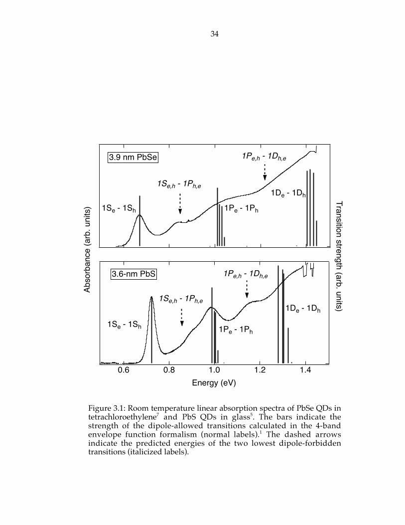
34
3.9 nm PbSe
1Se,h - 1Ph,e
1Pe,h - 1Dh,e
1Se - 1Sh 1Pe - 1Ph
1De - 1Dh
1.41.21.00.80.6Energy (eV)
3.6-nm PbS
1Se - 1Sh
1Se,h - 1Ph,e
1Pe - 1Ph
1De - 1Dh
1Pe,h - 1Dh,e
Abso
rban
ce (a
rb. u
nits
)
Transition strength (arb. units)
Figure 3.1: Room temperature linear absorption spectra of PbSe QDs intetrachloroethylene7 and PbS QDs in glass5. The bars indicate thestrength of the dipole-allowed transitions calculated in the 4-bandenvelope function formalism (normal labels).1 The dashed arrowsindicate the predicted energies of the two lowest dipole-forbiddentransitions (italicized labels).

35
3.2 Prior work
One experimental test of whether the true eigenstates of the QD are
simultaneously parity eigenstates is to compare the one and two-photon
absorption spectra.8, 9 If the QD wavefunctions are states of definite parity,
then the transitions observed in the one and two-photon absorption spectra
should be mutually exclusive: the one-photon spectra will connect states of
different parity whereas the two-photon spectra will connect states of the
same parity.
Kang proceeded to measure two-photon absorption spectra of PbS
quantum dots using a standard pump-probe technique.10 The data fail to show
the expected peak at the energy of the two-photon allowed 1P – 1 D resonance
(the 1S – 1P resonance is outside the spectral range that could be covered in
the experiment) and instead shows two strong resonances that are most likely
due to the two-photon forbidden 1P – 1P and 1D – 1D transitions. These
observations in the two-photon absorption spectra, when taken in conjunction
with one-photon spectra shown previously, indicate a failure to obey parity
selection rules.
Since the Pb-salt QDs have the rock-salt crystal structure and are inversion
symmetric, intrinsic mechanisms for the parity-breaking such as the internal
dipole field arising from the wurtzite crystal structure of CdSe and CdS QDs
are ruled out. Instead extrinsic effects, like surface defects or non-symmetric
shape or morphology were suspected to play a role. According to one
estimate, these effects could result in a strong mixing of the parity
eigenstates.10

36
Andreev et al. offered another mechanism to explain the additional
structure in the Pb-salt QD’s absorption spectrum. Working in the same 4-
band envelope function formalism, they fully included the anisotropy of the
bulk band structures of PbS and PbSe.2 The effects on the QD electronic states
were two-fold: (1) the isotropic states are split and their energies are shifted
and (2) the resulting anisotropic states are a linear superposition of different
isotropic states. This leads to several new parity-allowed transitions between
the anisotropy-modified electronic states.
When applied to a 8-nm diameter PbSe QD in a phosphate glass host,
Andreev et al. find good agreement between the unexplained peaks in the
measured absorption spectrum and their calculations. Therefore, they claim
that the inclusion of the anisotropy in the electronic structure calculations
accounts for all the features in the linear absorption spectrum. However,
absorption measurements of other Pb-salt QD samples conducted in our
laboratory fail to reflect such agreement with the anisotropic electronic
structure calculations. We pursued additional measurements to evaluate these
two possible explanations.
3.3 Parity-forbidden transitions between isotropic states versusparity-allowed transitions between anisotropy-induced states
Room-temperature linear absorption measurements were conducted on a
range of PbSe QDs sizes from a variety of different syntheses. Three different
sources were used for colloidal samples from the synthesis detailed in Chapter
2.7, 11 PbSe QDs embedded in a phosphate glass host, the same synthesis as the

37
2.2
2.0
1.8
1.6
1.4
1.2
1.0
(En,
exc.-
E bul
k)/(E
1,ex
c.-E b
ulk)
0.90.80.70.60.50.40.30.2E1,exc.-Ebulk
anisotropy transitions
allowed P - P transitions
Lipovskii IBM UR Evident Tech.
forbidden S - P transitions
allowed S - S transitions
Figure 3.2: The energy of the several lowest optical transitions in PbSeQDs6, 7, 11 as determined from room-temperature linear absorptionspectra. The scaling of the axes is described in the text. The horizontallines indicate the predicted energies of dipole-allowed transitions anddipole forbidden transitions within the isotropic model1 along withparity-allowed transitions within the anisotropic model.2

38
PbSe QDs used by Andreev et al., were also examined.6 The positions of the
lowest several absorption peaks were determined. In all samples, the first and
second peaks were visible and when the sample quality was good enough
(narrow enough size distribution), the third peak was also recorded.
Our findings are summarized in Figure 2. On the vertical axis, we plot the
confinement energy of the Nth exciton state scaled by that of the lowest
exciton and on the horizontal axis, the confinement energy of the lowest
exciton state (essentially the QD size). Representing the data in this manner
collapses the same transitions from different QDs sizes onto a horizontal line.
The energies of the allowed electronic transitions predicted by the isotropic
and the anisotropic models are shown. In addition, we calculate the position
of the parity-forbidden transitions using the energies of the electron and hole
states from the isotropic model.
We find that an explanation of the second absorption peak in terms of
transitions between anisotropy-induced states significantly overestimates the
energy. In fact, the energy of the second transition in the anisotropy model
approaches that of the 1P – 1P dipole-allowed transition from Kang’s original
work.1 On the other hand, the description of the second peak as a parity-
forbidden 1S – 1P transition quite accurately reproduces the energy of the
feature for nearly all of the samples studied.
Other experiments have yielded results that contradict the predictions of
the anisotropic electronic structure calculations. Wehrenberg et al. studied the
optical bleaching of PbSe NCs caused by direct electron injection into the
QDs.12 These measurements were sensitive to both interband (electron-hole)
and intraband (electron-electron and hole-hole) transitions. The authors
confirmed the Se (h) – Ph (e) interband transition and also observed Se (h) – Pe (h)

39
intraband transitions. However, they did not observe the features predicted to
only occur within the anisotropic model (for instance, the h3,h4 – e1,e2
interband transition, following the notation of Andreev et al.13). We take these
results as further evidence supporting the assignment of the second peak as a
parity-forbidden transition and not as a transition between anisotropy-
induced states.
However, recent electronic structure calculations of PbSe nanocrystals
(NCs) using tight-binding methods have called the explanation of the second
absorption peak in terms of parity-forbidden transitions into question.
Although Allan et al. did find that consideration of NCs with more complex
shapes and less symmetries slightly relaxes the parity selection rule, they were
never able to reproduce the experimentally observed oscillator strength of the
second absorption peak.4 Obviously, this argues against Kang’s hypothesis
that strong parity eigenstate mixing results from the break-down of inversion
symmetry at the QD surface.10
Although the mechanism remains in question, the experimental evidence
still strongly supports the assignment of the second absorption peak as a S – P
interband transition. In fact, our recent measurements that time-resolved the
excited state relaxation of electrons and holes in PbSe QDs showed that the
first and second transitions share a common state, 1Se (h). Therefore, we
consider another possible explanation for the second absorption peak that
does not violate the parity selection rule, an electric quadrupole transition.

40
3.4 Quadrupole transitions
The interaction between a quantum dot and an optical field may be described
semi-classically by use of a multipolar expansion of the interaction
Hamiltonian.14 For far-field excitation the first term in this expansion, the
electric dipole term, gives rise to a response that is considerably stronger than
that produced by subsequent terms. This is because the physical dimension of
the QD is much smaller than the wavelength of the light and also because of
the weak spatial variation of the field.
It has been shown by Zurita-Sanchez et al. that in cases where the spatial
variation of the optical fields is much stronger, as is the case in near-field
excitation, the higher terms in the multipolar expansion cannot be ignored.14
For instance the next higher terms, the electric quadrupole and magnetic
dipole, respond to the gradient of the electric field. Thus, in cases of large field
gradients, the optical absorption spectrum is modified by the inclusion of
electric quadrupole transitions of strength comparable to the electric dipole
transitions. However all of the experimental situations under which the extra
absorption features have been observed employed plane-wave optical
excitation. The quadrupole response to this applied field should be negligible
when compared to the electric dipole response.
The calculations by Zurita-Sanchez et al. are specific to a semiconductor
QD with hole wavefunctions expanded in p-like basis states and electron
wavefunctions expanded in s-like basis states, like II-VI and III-V materials.14
However for Pb-salt QDs, both electrons and holes are expanded in the same
set of basis states. This leads to additional terms in the interband matrix
elements that are not present in II-VI and III-V semiconductor QDs.1 We

41
considered the possibility of an unique and large contribution to the
quadrupole transition moment in IV-VI QDs that could compensate for the
small field gradient of the applied electric field.
We analytically evaluated the quadrupole moment for PbSe QDs (see
Appendix). The magnetic dipole moment has been ignored; generation of the
necessarily large magnetic field srengths requires the use of an azimuthally-
polarized optical near-field.15 Although not all of the necessary parameters are
available from k•p theory, we numerically estimate the order of magnitude of
the quadrupole moment and find it is smaller than the dipole moments by a
factor of approximately the wavelength of light squared. Therefore, it appears
that the only way to have an electric quadrupole transition of strength
comparable to an electric dipole transition is with application of a large field
gradient. However, might it be possible that the applied plane-wave excitation
develops a substantial gradient in the vicinity of the QD due to dielectric
effects? This is our next consideration.
The dielectric theory of nanostructures is a current and important topic of
theoretical and experimental studies. It was shown experimentally using
electrostatic force microscopy that the static dielectric constant of a single
CdSe NC is uniform and consistent with the value of the bulk
semiconductor.16 Recent calculations by Delerue et al. have shown that, with
the exception of a surface layer with a thickness on the order of the inter-
atomic spacing, the bulk value of the semiconductor dielectric function is
recovered inside the nanoparticle.17 Given these results, it is reasonable to
model the dielectric response of the QD as a solid sphere of the bulk dielectric
constant ε2. Let this sphere then be immersed in background dielectric ε1 (ε2 >
ε1) that contains an initially uniform electric field.

42
This problem is one solved in basic electrostatics.18 Outside, the initially
uniform field is distorted by the presence of the dielectric sphere. Inside the
sphere, the field remains uniform although its magnitude is reduced by a local
field factor,
F =
3ε1
ε2 + 2ε1(3.1)
Therefore, this simple model illustrates the lack of an electric field gradient in
the interior region of the QD. However, in light of Delerue’s calculations, we
should expect a field gradient at the surface. Let us estimate its magnitude,
| ΔE / Δz |.
Given their large dielectric constants (ε(∞) = 18 for PbS, 22 for PbSe19) the
dielectric screening is very strong for the Pb-salts. For instance, a PbSe sphere
immersed in air has a local field factor, F ~ 1/8. Therefore, the internal field is
reduced to about 10% of the magnitude of the externally applied electric field.
In addition, this reduction in the field strength occurs on a length scale of
atomic dimensions, say approximately the lattice constant. Therefore,
ΔEΔz
≈0.9E0
0.6 nm≈ 1.5 E0
nm(3.2)
For comparison, the estimated electric field gradient from the optical near-
field excitation scheme described by Zurita-Sanchez is ~ 0.5 E0 / nm.14
Yet, it is difficult to explain how electrons delocalized in the core of the QD
could couple effectively to this gradient existing at the surface. However, it is
possible that surface localized electrons or holes would couple exceptionally-
well to this field gradient. The intrinsic gap states proposed by Sercel et al.

43
would be one such possibility.20 Experiments are currently underway to
address the role of these and other dielectric effects on the optical and
electronic properties of the Pb-salt QDs.
3.5 Conclusions
We have reviewed the prior explanations for the unexplained structure
observed in the absorption spectra of high-quality Pb-salt QDs. It was shown
that the energy positions of these absorption peaks are better explained by the
parity-forbidden transitions between isotropic electronic states rather than
parity-allowed transitions between anisotropic electronic states. It was
suggested that deviations from inversion symmetry near the nanocrystal
surface were responsible for the parity-breaking. Recent atomistic electronic
structure calculations have called this hypothesis into question; the predicted
strength of the parity-forbidden transitions is always much weaker than that
observed in experiment.
As one possible explanation, we have considered the role of electric
quadrupole transitions. Under conditions of large applied electric field
gradients, quadrupole transitions have been shown to modify the optical
absorption spectrum. While the measurements revealing the unexplained
absorption structure were conducting using far-field optical excitation, we
propose that the strong dielectric screening experienced by the Pb-salt QDs
could generate a surface-localized electric field gradient comparable in
magnitude to that obtained in near-field experiments. Experiments are
currently underway to address the role of these dielectric effects on the
properties of lead-salt QDs.

44
References
1 I. Kang and F. W. Wise, Journal of the Optical Society of America B(Optical Physics) 14, 1632 (1997).
2 A. D. Andreev and A. A. Lipovskii, Physical Review B (CondensedMatter) 59, 15402 (1999).
3 G. E. Tudury, M. V. Marquezini, L. G. Ferreira, et al., Physical Review B62, 7357 (2000).
4 G. Allan and C. Delerue, Physical Review B.
5 N. F. Borrelli and D. W. Smith, Journal of Non-Crystalline Solids 180, 25(1994).
6 A. Lipovskii, E. Kolobkova, V. Petrikov, et al., Applied Physics Letters71, 3406 (1997).
7 H. Du, C. L. Chen, R. Krishnan, et al., Nano Letters 2, 1321 (2002).
8 K. I. Kang, B. P. McGinnia, Y. Z. Hu, et al., Physical Review B 45, 3465(1992).
9 M. E. Schmidt, S. A. Blanton, M. A. Hines, et al., Physical Review B 53,12629 (1996).
10 I. Kang, Ph.D. thesis, Cornell University, Ithaca, NY, 1998.
11 C. B. Murray, S. Sun, W. Gaschler, et al., IBM Journal of Research andDevelopment 45, 47 (2001).

45
12 B. L. Wehrenberg and P. Guyot-Sionnest, Journal of the AmericanChemical Society 125, 7806 (2003).
13 A. D. Andreev, E. Kolobkova, and A. Lipovskii, Journal of AppliedPhysics 88, 750 (2000).
14 J. R. Zurita-Sanchez and L. Novotny, Journal of the Optical Society ofAmerica B (Optical Physics) 19, 1355 (2002).
15 J. R. Zurita-Sanchez and L. Novotny, Journal of the Optical Society ofAmerica B (Optical Physics) 19, 2722 (2002).
16 T. D. Krauss and L. E. Brus, Material Science and Engineering B69-70,289 (2000).
17 C. Delerue, M. Lannoo, and G. Allan, Physical Review B 68, 115411(2003).
18 J. D. Jackson, Classical Electrodynamics (Wiley, 1998).
19 O. Madelung, M. Schultz, and H. Weiss, Landolt-Bornstein: NumericalData and Functional Relationships in Science and Technology (New Series)(Springer-Verlag, 1982).
20 P. C. Sercel, A. L. Efros, and M. Rosen, Physical Review Letters 83, 2394(1999).

46
Chapter 4Photoluminescence studies of lead-salt nanocrystals
4.1 Introduction
Lead-salt quantum dots (QDs) are among the few materials that can provide
size-quantized electronic transitions at technologically-important infrared
wavelengths. Structures containing these QDs may find use in optoelectronic
applications as well as in biophysical applications such as fluorescence
microscopy. Beyond the initial characterization studies, such as those
presented in Chapter 2, work on the emission properties of these QDs has
concentrated on application-related aspects.1, 2 However, there is a lack of
understanding of the emission characteristics of PbSe QDs.
For instance, the 50 to 100 meV Stokes shift observed in global
photoluminescence (PL) measurements, while not interpreted directly in
terms of the homogeneous spectrum and intrinsic nanocrystal properties, does
nevertheless, suggest a Stokes shift in the single-particle spectrum.3 This may
arise from the vibronic nature of the transitions. Although the coupling of
excitons to optical phonons is expected to be very weak in PbSe, phonon-
assisted transitions may be strong due to non-Franck-Condon effects.4
In addition, the observed photoluminescence decay times are longer than
expected for a dipole transition. A straightforward calculation of the transition
dipole of the lowest exciton in PbSe QDs yields a radiative lifetime on the
order of nanoseconds. Dielectric screening would be expected to increase the
lifetime by as much as two orders of magnitude if the bulk dielectric constants
of PbSe are assumed. However, recent measurements that tested this

47
simplistic dielectric screening hypothesis by the systematic variation of the
host dielectric constant appear not to follow the proper trend.5 More generally,
it is also surprising that the luminescence properties of QDs can be explained
in terms of only intrinsic volume states when a large portion of the atoms
comprising a QD lie at the surface. In fact, recent far-infrared absorption
measurements of PbSe QDs reproducibly observed the presence of mysterious
high-frequency absorptions that cannot be explained by treating the QD as
truncated crystalline lattice.6
The topic of fine structure in the energy spectra of QDs has been a subject
of much interest and has been invoked to explain the shift between absorption
and emission peaks as well as the observation of long radiative lifetimes in
CdSe.7, 8 Kang’s envelope function calculations of the electronic structure of the
IV-VI QDs did include these many-body perturbations. Their effects are as
follows: the Coulomb interaction does not split the lowest transition and the
exchange interaction is small (10 meV in comparison to ~ 1 eV transition
energy).9 Still, other effects that are expected to influence the electronic spectra
cannot be included in envelope function methods. Features like the multi-
valley nature of the IV-VI semiconductors and the influence of the surfaces
(surface molecules or surface reconstruction) have been addressed with tight-
binding theories.10-12
Here, we report studies of the band-edge electronic structure of PbSe and
PbS QDs using PL spectroscopies. We observe, for the first time, a splitting in
the PL spectrum that is also consistent with a calculation of the splitting from
intervalley coupling. Size-selective PL measurements reveal broad emission
lines even when the inhomogeneous broadening effects of the size distribution
are eliminated suggesting that the degeneracies arising from the different

48
valleys are also split by other mechanisms. We also observe that the surfaces
do impact some of the emission properties and we consider explanations for
all for all of these features.
4.2 Sample preparation and initial characterization
High-quality colloidal PbSe and PbS NCs were synthesized as reported
previously in the literature. To perform temperature-dependent
measurements, an optically transparent low-temperature host is required.
Several suitable low-temperature glass formers, typically used in the visible
region of the electromagnetic spectrum, were reviewed; however, all of these
compounds have absorptions in the infrared. For instance, 2,2,4,4,6,6,8-
heptamethylnonane (HMN) absorbs for wavelengths > 1500 nm, precluding
optical measurements of larger QDs in this host.
To circumvent this problem with low-temperature hosts, we fabricated
solid-state films by drop-casting the QDs from hexane onto a glass coverslip.
Visual inspection reveals light and dark regions, indicating that the films do
not layer uniformly. This is expected; the hydrophobic QDs should cluster on
hydrophilic glass surface, leading to many separated domains on the surface.13
However, the optical measurements probe large regions of the sample and
therefore average over the different domains. Room-temperature absorption
and photoluminescence spectra were measured immediately after the films
were prepared and their spectral features did not change in the span of several
weeks over which our experiments were conducted.

49
1.2
1.0
0.8
0.6
0.4
0.2
0.0
Abs,
PL
(Nor
mal
ized)
1.51.41.31.21.11.00.90.8Energy (eV)
T = 298 K Abs:
solid state film colloid
PL:
solid state film colloid
Figure 4.1: Comparison of the absorption and PL spectra in solid statefilm samples and colloidal samples. The solid state film absorption hasbeen corrected for scatter by subtracting a 1/l4 background. The peak infilm absorption at ~ 0.9 eV is from oleic acid.

50
The samples were loaded into a Helium vapor cryostat and cooled to
temperatures as low as 15 K. The PL was excited with the spectrally-resolved
emission from a tungsten-halogen lamp or one of several narrow-band laser
sources: a home-built continuous-wave Ti:sapphire laser (775 - 930 nm), a
commercial grating-tuned diode laser (1520 – 1570 nm), and a fixed
wavelength diode laser (~ 980 nm). The emitted light was collected at right
angle to the excitation, spectrally-resolved by a 0.2-meter monochromator, and
detected with a TE-cooled extended InGaAs photodiode. The spectral
resolution of the system was typically less than 5 meV.
Room-temperature optical absorption spectra of the solid state films reveals
the same excitonic structure as in the colloids from which they were made
although superimposed on a scattering background (Figure 4.1). The PL from
the films is still dominated by band-edge emission although we consistently
find that the emission spectra are red-shifted and narrower than that from the
colloids. Transmission electron micrographs of similar film assemblies of PbSe
QD show nearly close-packed ordering within a given domain, likely
separated by the surface ligands (oleic acid ~ 2 – 3 nm, head-to-tail).3 Given
these features in the structural characterization, we tentatively attribute the
narrowing and red-shifting of the emission spectra to electronic energy
transfer (EET) between the NCs.
EET is a one-step process in which energy is simultaneously transferred
from an excited species (donor) to an unexcited species (acceptor). In this way,
it is distinct from radiative transfer in which an intermediate photon is first
emitted by the donor and then absorbed by the acceptor. EET has been
previously observed in close-packed arrays of CdSe QDs14 but this is its first
observation with PbSe NCs. Work is currently underway to address this topic
51
in more detail. In the remainder of this work, we consider EET as only a
mechanism that reduces the inhomogeneous broadening effects of the QD size
distribution on the emission spectra.
4.3 Global photoluminescence measurements
Figure 4.2 shows the change in the PL spectrum with temperature for a solid
state film of 3.7-nm PbSe NCs. It is important to note that that the excitation
photon energy is well above the energy of the lowest transition. In this case,
all of the QDs in the sample, regardless of their size, are excited and contribute
to the ensemble emission spectrum. This is referred to as global excitation.
Figure 4.2 confirms that the resulting PL spectrum is broad and comparable to
the width of the absorption peaks (see for example, Figure 1) suggesting that
the bandwidth is a consequence of the particle-size distribution.
As the temperature decreases, the peak energy of the emission spectrum
shifts to lower energy. However, in films of smaller QDs, the peak barely
shifts at all. These observations are consistent with the size-dependent
temperature variation of the lowest transition of PbSe QDs by Olkovets et al.15
We also observe that the shape of the low-temperature PL spectrum is
different than the spectrum measured at room temperature.
To investigate whether this structure in the PL spectrum might be due to
sample preparation, we also performed low-temperature PL measurements on
colloidal samples in HMN. Figure 4.3 shows the low-temperature emission
spectra for PbS QDs in colloidal and solid state film preparations. Although
the strength of the two PL features located at approximately 0.97 eV and

52
1.0
0.8
0.6
0.4
0.2
PL (N
orm
alize
d)
1.11.00.90.80.7Energy (eV)
3.7-nm PbSe Temperature:
300 K 170 K 15 K
Figure 4.2: The peak of the PL spectrum shifts to lower energy andnarrows with decreasing temperature. The excitation energy is 1.1 eV.The feature observed in all of the traces at 0.9 eV is an artifact of thegrating.
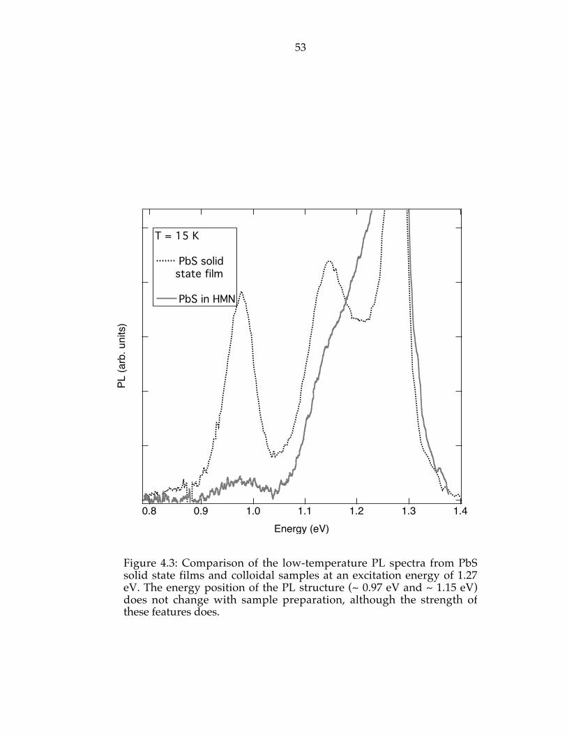
53
Figure 4.3: Comparison of the low-temperature PL spectra from PbSsolid state films and colloidal samples at an excitation energy of 1.27eV. The energy position of the PL structure (~ 0.97 eV and ~ 1.15 eV)does not change with sample preparation, although the strength ofthese features does.
PL (a
rb. u
nits
)
1.41.31.21.11.00.90.8Energy (eV)
T = 15 K
PbS solidstate film
PbS in HMN

54
1.1 eV does change with sample preparation, it is important to note that their
position does not.
Additionally, we measured the intensity dependence of the emission
spectrum by using continuous-wave and pulse laser excitation. Typically, the
emission resulting from carriers trapped at surface sites exhibits a different
intensity dependence than the emission from the intrinsic core states of the
QD.16 We find that PL spectrum maintains its shape even as the peak intensity
of the excitation light is varied by a factor of ~ 1010 (Figure 4.4). We take both
of these observations as experimental evidence that the structure in the PL
spectrum is not solely an extrinsic surface effect.
Figure 4.5 displays the PL spectra measured at 15 K for 3 different sizes of
PbSe QDs. A clearly-discernable second peak is observed on the low-energy
side in the small PbSe sample. Although the larger-sized PbSe QDs exhibit no
obvious second peak, their PL spectra are asymmetric with a tail extending on
the low-energy side. Also shown in Figure 4.5, is the systematic
decomposition of each of these PL spectra into a sum of two Gaussians. For
smaller sized QDs, we find that the width of the Gaussians and also their
separation is larger. The separation between the peaks varies from ~ 20 meV
to 130 meV as the PbSe QD size decreases from 4.6 nm to 3.2 nm. A 2-nm
diameter PbS QD (not shown here) exhibits a peak separation of ~ 310 meV.
4.4 Size-selective photoluminescence measurements
In the measurements presented so far, the widths of the emission peaks were
reflective of the size distribution rather than any intrinsic NC properties. One

55
1.0
0.8
0.6
0.4
0.2
0.0
PL (N
orm
alize
d)
1.21.11.00.90.80.7Energy (eV)
T = 298 K 3.2-nm PbSe Peak intensity:
CW, 0.8 W/cm2
pulsed, 50 GW/cm2
Figure 4.4: The intensity dependence of the PL spectra was exploredusing CW and pulsed excitation. The measured spectra are nearlyidentical despite a difference in peak intensity of approximately 1010.Based on this observation, we rule out contributions from surfacestates.
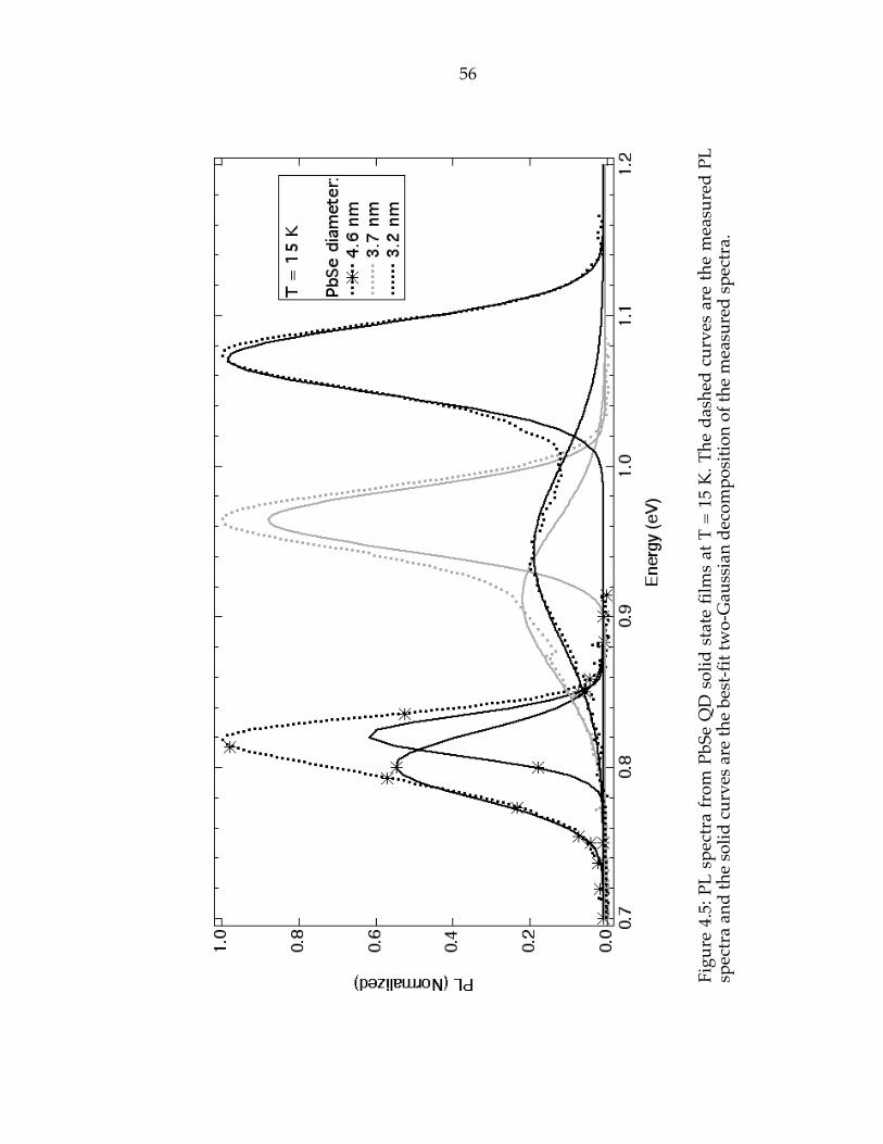
56
F i g u r e 4 . 5 :Photoluminescence spectrafrom PbSe QD solid statefilms at T = 15 K. Thedashed curves are themeasured PL spectra andthe solid curves are thebest-fit two-Gaussiandecomposition of themeasured spectra.
Figu
re 4
.5: P
L sp
ectra
from
PbS
e Q
D so
lid st
ate
film
s at T
= 1
5 K.
The
das
hed
curv
es a
re th
e m
easu
red
PLsp
ectra
and
the s
olid
curv
es a
re th
e bes
t-fit
two-
Gau
ssia
n de
com
posit
ion
of th
e mea
sure
d sp
ectra
.

57
way to circumvent this inhomogeneous broadening effect on the emission
spectra is to utilize size-selective excitation. In contrast to the global excitation
experiments discussed above, a narrow-band excitation source with a photon
energy tuned within the low-energy tail of the QD absorption spectrum is
used to photo-excite only the largest QDs within the sample. Subsequently,
only this subset of the largest QDs contributes to the line-narrowed emission
spectrum. Based on the availability of laser sources in our laboratory, we
measured line-narrowed emission from one sample. The results are shown in
Figure 4.6 for a 4.7-nm PbSe QD.
Compared to the globally-excited emission, the bandwidth of the features
observed using size-selective excitation is narrower. However, the bandwidth
is still broader than that observed for CdSe QDs in either size-selective PL (1 –
10 meV) 17 or single-dot PL (< 1 meV) experiments.18 Another interesting
feature is the appearance of strongly anti-Stokes shifted (A-S) PL in the case of
the reddest excitation (0.790 eV).
4.5 Discussion
One possible explanation of the splitting observed in the PL spectra involves
the degeneracy splitting of the lowest transition via the coupling of equivalent
L-valleys. Allan et al. have performed a calculation of the intervalley splitting
and show it to be effectively large.12 In Figure 4.7, the maximum energy
splitting from this calculation is compared to the measured energy separation
of the two PL features obtained from the Gaussian decomposition of the
global PL spectra over a range of temperatures. The calculation and
measurements agree quantitatively over the range of sizes studied here.

58
1.0
0.8
0.6
0.4
0.2
0.0
PL (N
orm
alize
d)
0.850.800.75Energy (eV)
T = 15 K PL excitation energy:
0.790 eV 0.816 eV
0.953 eV 2 Gaussian
decomposition
Figure 4.6: Line-narrowed PL from 4.7-nm PbSe at T = 15 K. The firstabsorption peak (not shown) is at 0.95 eV. The size-selective excitationis tunable between 0.816 and 0.790 eV. The solid lines labeled withmarkers represent the line-narrowed emission spectra. The solid blacklike is the globally-excited PL spectrum and the dashed lines show thebest-fit two Gaussian decomposition of the global PL spectrum fromFigure 4.5.

59
140
120
100
80
60
40
20
Ener
gy s
epar
atio
n (m
eV)
5.04.54.03.53.0Diameter (nm)
PbSe: T= 15 K T = 90 K T = 298 K
Allan's calculated
max intervalley splitting
Figure 4.7: The experimentally measured PL feature splitting for threedifferent PbSe QD sizes. The splitting is found to increase with bothdecreasing temperature and size. We compare these measurements tomaximum splitting predicted in calculations by Allan et al.

60
Another mechanism we are currently pursuing to explain the PL splitting
involves the role of the intrinsic gap states proposed by Sercel et al.20 Though
we lack a quantitative understanding of these states in PbSe at the moment,
qualitatively, these gap states are predicted to play an increasing role in small
QDs. For instance, transitions between the gap states and the conduction band
could determine the absorption band edge in the smallest QDs.20
The explanation for the broad emission lines observed in size-selective
excitation experiments is likely the result of additional degeneracy splittings.
The lowest transition will be composed of 64 lines which are shifted by
different effects: Coulomb interaction, exchange interaction, inter-valley
couplings and shape asymmetry effects.12, 19
The A-S PL is difficult to explain. The presence of a decaying A-S tail in PL
has been observed previously at room-temperature. It was explained by
models involving surface states in energetic proximity to the intrinsic QD core
state, and the energy up-conversion occurred by phonon absorption.21
Generally, it is a feature of II-VI and III-V semiconductor QDs for surface
ligands and surface reconstruction to have a major influence on the band-edge
electronic states and optical properties.11, 22
However, it is difficult to explain the strongly-peaked A-S PL (~ 10 meV)
in the case of PbSe. Though this energy is the same order of magnitude as the
phonon energy in PbSe (~ 17 meV), these vibrational modes should not be
populated at low temperature. Additionally, PbSe appears to be more
resistant to the deleterious surface effects like dangling bonds. Atomistic
calculations have found that PbSe, because of its large ionicity, does not
require special care to saturate dangling bonds and remove surface states from

61
the energy gap.10 This may also explain the high PL efficiency in PbSe QDs
and also why no trapped states have been observed experimentally.12
4.6 Conclusions
In conclusion, we report photoluminescence (PL) studies of the band-edge
electronic structure of PbSe and PbS QDs using PL spectroscopies. We
observe, for the first time, a splitting in the emission spectrum. The splitting
increases as the QD size is decreased and is also approximately a factor of two
larger in PbS than in PbSe. The magnitude of this splitting and its variation
with QD size is consistent with a calculation of the splitting of the lowest
transition due to the coupling of equivalent L-valleys. The role of intrinsic gap
states could be another way to explain the splitting in the PL spectra. Size-
selective PL measurements reveal broad emission lines even when the
inhomogeneous broadening effects of the size distribution are eliminated. This
suggests that the energy level degeneracies are also split by other mechanisms
including the Coulomb interaction, exchange interaction, and shape
asymmetry effects. We also find that the surfaces do impact the strength of the
emission features but not their energies. This is, perhaps, a reflection of the
robustness of PbSe QDs against the formation of surface states.

62
References
1 L. Bakueva, S. Musikhin, M. A. Hines, et al., Applied Physics Letters 82,2895 (2003).
2 J. S. Steckel, S. Coe-Sullivan, V. Bulovic, et al., Advanced Materials 15,1862 (2003).
3 H. Du, C. L. Chen, R. Krishnan, et al., Nano Letters 2, 1321 (2002).
4 E. P. Pokatilov, S. N. Klimin, W. M. Fomin, et al., Physical Review B.Condensed Matter 65, 075316 (2002).
5 S. W. Clark, unpublished.
6 B.-H. Hyun, unpublished.
7 M. Chamarro, C. Gourdon, P. Lavallard, et al., Physical Review B 53,1336 (1996).
8 M. Nirmal, D. J. Norris, M. Kuno, et al., Physical Review Letters 75,3728 (1995).
9 I. Kang and F. W. Wise, Journal of the Optical Society of America B 14,1632 (1997).
10 G. Allan, Physical Review B (Condensed Matter) 43, 9594 (1991).
11 S. Pokrant and K. B. Whaley, The European Physics Journal D 6, 255(1999).
12 G. Allan and C. Delerue, Physical Review B.

63
13 K. Du, private communications.
14 C. R. Kagan, C. B. Murray, and M. G. Bawendi, Physical Review B(Condensed Matter) 54, 8633 (1996).
15 A. Olkhovets, R.-C. Hsu, A. Lipovskii, et al., Physical Review Letters 81,3539 (1998).
16 F. Hache, M. C. Klein, D. Ricard, et al., Journal of the Optical Society ofAmerica B 8, 1802 (1991).
17 M. Nirmal, C. B. Murray, and M. G. Bawendi, Physical Review B(Condensed Matter) 50, 2293 (1994).
18 S. A. Empedocles, D. J. Norris, and M. G. Bawendi, Physical ReviewLetters 77, 3873 (1996).
19 A. L. Efros, private communications.
20 P. C. Sercel, A. L. Efros, and M. Rosen, Physical Review Letters 83, 2394(1999).
21 E. Poles, D. C. Selmarten, O. I. Micic, et al., Applied Physics Letters 75,971 (1999).
22 H. Fu and A. Zunger, Physical Review B (Condensed Matter) 56, 1496(1997).
64
Chapter 5Time-Resolved Intraband Relaxation of Strongly-Confined Electrons and Holes in Colloidal PbSeNanocrystals
The relaxation of strongly-confined electrons and holes between 1P and 1S
levels in colloidal PbSe nanocrystals has been time-resolved using
femtosecond transient absorption spectroscopy. In contrast to II-VI and III-V
semiconductor nanocrystals, both electrons and holes are strongly confined in
PbSe nanocrystals. Despite the large electron and hole energy level spacings
(at least 12 times the optical phonon energy), we consistently observe
picosecond time scale carrier relaxation. Existing theories of carrier relaxation
cannot account for these experimental results. Mechanisms that could possibly
circumvent the phonon bottleneck in IV-VI quantum dots are discussed.
5.1 Introduction
A dramatic reduction in the relaxation rate of carriers in three dimensionally-
confined quantum systems is predicted to occur if the energy-level spacing is
several times greater than the phonon energy.1, 2 While an interesting scientific
issue in nanocrystal physics, this “phonon bottleneck” would also have major
implications for applications of quantum dots (QDs). In a QD gain medium,
for instance, excited carriers should rapidly relax non-radiatively to their
lowest states before the emission of a photon.
65
In prior experiments on colloidal QDs, ultrafast intraband carrier
relaxation has been observed and a mechanism explaining the process has
been widely adopted. This “Auger-like” electron-hole scattering process,
described by Efros et al., relies on the high density of hole states in II-VI and
III-V semiconductor QDs plus the assumption of fast hole relaxation via
phonon emission.3 In this case, electron relaxation occurs by coupling to the
large density of hole states and happens on a picosecond to sub-picosecond
time scale. The strongest evidence in support of the Auger-like process comes
from experiments in which this mechanism is intentionally obstructed. When
the electron is forced to relax in the absence of a spectator hole, an increase of
an order-of-magnitude in the relaxation time is observed.4-6 It remains a
mystery how the intraband relaxation occurs without the Auger-like
mechanism.
QDs of the IV-VI semiconductors PbS, PbSe, and PbTe differ substantially
from their II-VI and III-V counterparts. With large electron and hole Bohr radii
(for example, in PbSe: ae,= 23 nm, ah = 24 nm), both electrons and holes are
strongly confined. This leads to simple and sparse energy spectra for IV-VI
QDs.7 Such materials should be ideal for studying electron dynamics in a
system with energy levels spaced more than a phonon-energy apart. In
contrast, the electron is confined only in small II-VI and III-V QDs, and the
hole is never strongly confined (for example, in CdSe: ae = 3 nm, ah = 1 nm). In
addition, the confinement-induced coupling between the three (heavy-hole,
light-hole, and split-off) valence bands further complicates the already dense
ladder of hole states and leads to congested energy spectra in II-VI and III-VI
QDs. Intraband electron relaxation in II-VI and III-V nanocrystals4-6 is
dominated by processes that cannot occur in IV-VI materials, so studies of

66
electron relaxation in II-VI and III-V nanocrystals do not provide direct
information about the relevant processes in IV-VI structures.
A consequence of the sparse spectra of IV-VI QDs is that carrier relaxation
via the Auger-like process should be impossible. Therefore, it is surprising that
prior studies of IV-VI QDs did not observe a phonon bottleneck.8, 9 Here, we
report the first experiments to directly time-resolve the intraband electron and
hole relaxation in strongly-confined colloidal PbSe nanocrystals.10 At low
photo-excited carrier density, the 1P to 1S relaxation time is observed to
increase from 3 to 9 ps as the QD diameter increases from 4.3 to 6.0 nm. At
high carrier density, the relaxation time ranges between 2 and 3 ps. In cases
where carriers are pumped into higher excited states, we observe a relaxation
time of ~3 ps, independent of the carrier density. No known mechanism
accounts for these fast relaxations, and some possibilities are discussed.
5.2 Experiment
High-quality colloidal PbSe NCs were synthesized as reported previously in
the literature11, 12. A colloidal silica host was developed and the PbSe QDs were
dispersed into the matrix13. The resulting solid films were 240-µm thick and
contained approximately 0.1% volume occupancy of QDs. Optical
characterization of the films reveals excitonic structure in the absorption and
emission spectra, as well as photoluminescence lifetimes comparable to those
of the colloids (Figure 5.1).
The electronic structure of PbSe and PbS NCs was calculated by Kang et al.
using a 4-band envelope function formalism.14 The first 2 electron and 2 hole

67
Transition strength (arb. units)
1.41.21.00.80.6Energy (eV)
Abs,
PL
(arb
. uni
ts)
1Se-1Sh
1Pe-1Ph
1Se(h) -1Ph(e)
Figure 5.1: The absorption (solid line) and photoluminescence (shadedregion) spectra for 6-nm PbSe QDs in the colloidal silica film. Thelowest few electronic states are calculated using a 4-band envelopefunction formalism (inset). The strength of the lowest dipole-allowedtransitions are indicated by vertical lines. The second absorptionfeature (italicized label) is discussed in the text. Separate controlmeasurements of a blank film show that the absorption peak near 0.6eV is due to the host.

68
states and the lowest dipole-allowed transitions for a 6-nm diameter PbSe QD
are shown in Figure 5.1. The states are labeled by total angular momentum (j)
and parity (π) but for simplicity, we adopt the usual nomenclature and refer to
the states according to the angular momentum of the envelope function
( = 0 , 1… as S, P,…). To date, electronic-structure calculations of Pb-salt QDs
fail to reproduce the second absorption peak and some attention has been
paid to this previously14,9, 15-18. The energy of this peak matches that of the
dipole-forbidden transitions between 1Se (h) and 1Ph (e) states. However, Allan et
al. did not find significant strength for these transitions even when
considering asymmetric QDs in their tight-binding calculations18. Still, we are
intrigued to find that our ultrafast measurements support the assignment of
the second absorption peak to 1Se (h) - 1Ph (e) transitions (see below). The nature
of these unexplained transitions will be more fully addressed in a future work
but in the remainder of this chapter, we will assume this peak arises from 1Se
(h) - 1Ph (e) transitions. For the PbSe QD sizes studied here, the 1Pe (h) to 1Se (h)
energy spacing is between 200 and 300 meV.
The vibrational modes are also modified by confinement and in QDs of
polar materials, the optical mode with = 0 is expected to contribute most
strongly to relaxation by phonon emission. As shown in recent experiments by
Hyun et al., this mode has an energy of approximately 17 meV over the range
of QD sizes studied here19. Under these circumstances, a phonon bottleneck is
expected because the 1Pe (h)-1Se (h) energy spacing is 12 to 18 phonon energies.
Two-color transient absorption experiments were performed to investigate
the intraband carrier dynamics. In this experiment, a strong pump pulse
incident on the sample generates excited electron-hole pairs. A weak, time-
delayed probe pulse monitors the absorption of the lowest optical transition.

69
In the limit that αL < 0.1 (α is the linear absorption coefficient and L is the
propagation length), the differential transmittance (DT) of the probe beam,
ΔT/T0 = (T-T0)/T0, is directly proportional to the sum of the electron and hole
populations. Here, T and T0 are the probe beam transmission with and
without the pump. The subsequent relaxation of the photo-excited carriers is
observed by monitoring the DT as a function of the time delay between pump
and probe pulses. We are unable to separate electron and hole contributions to
the DT signal because of their similar electronic structures. Therefore, the
mirror image transitions are always implied.
The pump and probe pulses were generated in identical optical parametric
amplifiers (OPAs), simultaneously pumped by a Ti:sapphire regenerative
amplifier. Each OPA was tunable in wavelength from 450 to 3000 nm. The
pump and probe pulses were typically 100 fs in duration, and the time
resolution of the measurement was better than 300 fs for all combinations of
wavelengths employed in this work. The pump beam was mechanically
chopped and the probe beam was split into signal and reference beams and
measured in balanced detection using a lock-in amplifier. The probe beam was
always set to the peak absorption wavelength of the lowest optical transition,
1Se - 1Sh, and two different cases were investigated. In case 1, the pump beam
was tuned to the 1Se (h) - 1Ph (e) transitions. In case 2, carriers were excited into
much higher excited states by pumping with visible light (ω = 2.4 eV). The
pump pulse energies were typically varied over the range of tens to hundreds
of nanoJoules. All of the measurements presented here were conducted at
room temperature.
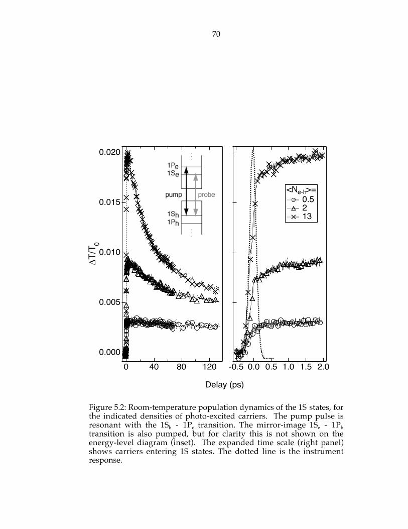
70
2.01.51.00.50.0-0.5
<Ne-h>= 0.5 2 13
0.020
0.015
0.010
0.005
0.000
ΔT/T0
12080400
Delay (ps)
Figure 5.2: Room-temperature population dynamics of the 1S states, forthe indicated densities of photo-excited carriers. The pump pulse isresonant with the 1Sh - 1Pe transition. The mirror-image 1Se - 1Phtransition is also pumped, but for clarity this is not shown on theenergy-level diagram (inset). The expanded time scale (right panel)shows carriers entering 1S states. The dotted line is the instrumentresponse.

71
ΔT/T
0 (no
rmal
ized)
1086420Delay (ps)
<Ne-h>= 13 2 0.5
Figure 5.3: The population dynamics of the 1Se - 1Sh transition under1Se (h) - 1Ph (e) excitation, for different excitation levels. <Ne-h> is theaverage number of photo-excited electron-hole pairs per QD. The timeat which the population peaks is extracted from a fit to the data (solidlines). The traces are normalized and then offset for clarity. The delaystage step size was changed at 2 ps, giving the appearance of an abruptchange in noise level.

72
1S - 1P Excitation
Figure 5.2 shows a typical measurement when the pump photon energy is
resonant with the 1Se (h) - 1Ph (e) transitions. In the left panel, we observe the
population of the 1S states increasing on the time scale of the pump pulse, and
then decaying within 40 to 100 ps. To focus on carriers entering 1S states, we
expand the time scale in the right panel.
The population of the 1S states exhibits two components, one rising within
the time duration of the pump pulse and the other rising for several
picoseconds thereafter. The energy-level diagram (Figure 5.2, inset) illustrates
their origin: (1) the component rising with the pump pulse develops because
the pumped and probed transitions share a state (in the case shown, 1Sh); thus,
one part of the transition is populated directly by the pump pulse, and (2) the
slower rising component is caused by carriers undergoing intraband
relaxation (1Pe to 1Se for the case shown). The first component supports our
assignment of the second absorption peak to 1Se (h) - 1Ph (e) transitions.
The magnitude of these signals also contains valuable information. We
would expect the fast and slow-rising components to contribute equally to the
total signal magnitude on the basis of the similar electronic structure.
However, the measurements indicate that the 1S states are almost 7-times
more likely to be populated by direct excitation than by the 1P to 1S
relaxation. This observation suggests the presence of an alternate decay
channel. However in what follows, we will focus on the 1P to 1S relaxation
process.
Figure 5.3 shows the DT traces for the sample in Figure 5.2 over a wider
range of carrier densities, but normalized to the peak DT. The curves are fit to

73
6.0
5.5
5.0
4.5
4.0
3.5
1P to
1S
rel
axat
ion
time
(ps)
6.05.55.04.54.0
QD diameter (nm)
<Ne-h> = 1
Figure 5.4: 1P - 1S relaxation time is plotted versus QD diameter.
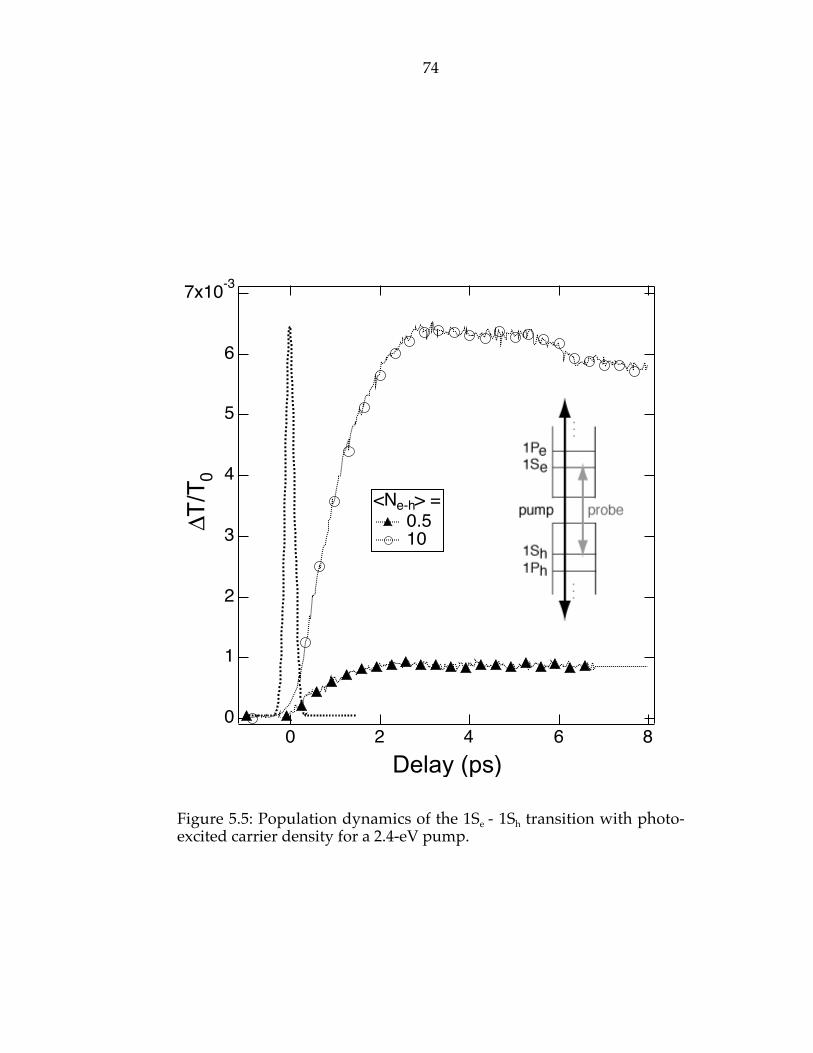
74
7x10⁻³
6
5
4
3
2
1
0
ΔT/T
0
86420Delay (ps)
<Ne-h> = 0.5 10
Figure 5.5: Population dynamics of the 1Se - 1Sh transition with photo-excited carrier density for a 2.4-eV pump.
75
extract the time at which the population of the 1S states peaks, and this is
taken to be the 1P to 1S relaxation time. With an average of 0.5 electron-hole
pairs per QD (<Ne-h> = 0.5), the relaxation is observed to occur in 6 ps, and this
time decreases as the photo-excited carrier density is increased. We observe
this trend in all of the QDs studied. The fastest relaxation time observed is 2
ps, which is approximately 3 – 4 times larger than the electron relaxation time
in bulk PbSe. We repeated these measurements on a range of QD sizes
between 4.3 and 6.0 nm and find the 1P to 1S relaxation time increases with
QD size (Figure 5.4). In these measurements the carrier density was kept low
to avoid multi-carrier effects in the relaxation.
High-energy excitation
We also explored the effect of exciting carriers far above the 1P states. This
has the advantage of not directly populating a state that is probed.
Accordingly, the rise of the 1Se - 1Sh population shown in Figure 5.5 now
consists of a single component. When a 4.9-nm-diameter QD is pumped at 2.4
eV, we find that the 1Se - 1Sh population develops in approximately 3 ps at
both low (<Ne-h> <1 ) and high (<Ne-h> = 10) carrier densities. This insensitivity
to carrier density is in contrast to the results obtained when exciting directly
into 1P states. Therefore, we need to consider these two regimes separately.
5.3 Discussion
We now turn to a discussion of the possible relaxation mechanisms. One way
to explain the intraband relaxation of carriers from states far above 1P (Figure
5.5) and the observed insensitivity to carrier density is impact ionization. In
this process, an electron with energy in excess of twice the 1Se - 1Sh energy

76
difference (ΔE1S-1S) relaxes to its 1S state by exciting additional electrons from
1Sh to 1Se.20 Thus, two or more cooled carriers may result from a single highly-
excited one. Schaller et al. have attributed the appearance of multi-exciton
signatures in the population decay of the 1S states with <Ne-h> < 1 to impact
ionization.21 At low carrier density and high-energy excitation (ω=2.5*ΔE1S-1S),
we also observe a fast decay component from the 1S states. We do not observe
this for 1S – 1P excitation.
The 1P to 1S relaxation requires a different explanation. Any possible role
of multi-carrier effects is excluded by consideration of the relaxation for <Ne-h>
< 1. Yet even in this case, the observed relaxation time is between 3 and 9 ps,
with the smallest QDs exhibiting faster relaxation. These results are in
reasonable agreement with the upper bound on the intraband relaxation time
set by Wehrenberg et al.9.
The contribution of multiphonon22 or polaron23 effects in the relaxation are
ruled out because they cannot account for efficient relaxation over such large
energy level spacings. However, there may be additional states that could
facilitate the relaxation. One possible source of such states is the four
equivalent L-valleys of PbSe. Splitting of these degenerate states is calculated
to be as large as ~100 meV in the smallest QDs.18 Even with such splitting,
however, the energy gap between the 1P and 1S manifolds would be several
phonon energies.24
It is also possible that the surface could play a role in the relaxation that we
observe. Darugar et al. have studied the relaxation from the lowest transition
in CdSe QDs and quantum rods and find that QDs relax faster than quantum
rods of the same diameter. Darugar et al. correlate this to the predicted change
in excited electron density on the nanostructure surface, and conjecture that

77
coupling between the excited electrons and large surface molecules could lead
to efficient carrier thermalization.25
Before concluding, we note the similarity in intraband relaxation times (1)
reported in this work for electrons and holes in PbSe QDs and (2) observed for
electrons in II-VI and III-V semiconductor QDs when the Auger-like electron-
hole scattering mechanism is intentionally obstructed.4-6 These results suggest
the existence of a non-radiative relaxation channel on the 1 to 10 ps time scale
that is accessible to strongly-confined electrons and/or holes in colloidal QDs,
independent of the material system. This too suggests that the surface may be an
integral part of the intraband relaxation mechanism. Renewed efforts to
incorporate the surface’s role into the relaxation may be needed.
5.4 Conclusions
In conclusion, we have time-resolved the relaxation of electrons and holes in
colloidal PbSe NCs. In stark contrast to other semiconductor NCs, both
electrons and holes are strongly confined in PbSe QDs. Therefore, Auger-like
electron-hole scattering cannot be invoked to explain the intraband relaxation
of charge carriers. In cases where carriers are pumped into higher excited
states, we observe a relaxation time of ~3 ps, independent of the carrier
density. We tentatively attribute this behavior to carrier cooling via impact
ionization. When the P states are directly populated with, on average, less
than one electron or hole per QD, the 1P to 1S relaxation time increases from 3
to 9 ps as the QD size is varied between 4.3 and 6.0-nm in diameter. The size
dependence of this relaxation may be correlated with the change in electron
density on the QD surface as previously suggested in the literature. This could

78
explain the similarity of the relaxation times observed in PbSe QDs and in
surface-modified colloidal II-VI and III-V QDs. Known mechanisms based on
interior electron states and vibrational modes cannot account for the
experimental results, which suggests that surface atoms and ligands may play
a major role.
5.5 Acknowledgements
This work was primarily supported by the Nanoscale Science and Engineering
Initiative of the National Science Foundation under NSF Award Number EEC-
0117770. The laser facility used for these experiments was supported under
NIH award 9 P41 EB001976-17 and NSF award CHE-0242328. We also thank J.
Gillies and D. Landry of Evident Technologies, Inc. (Troy, NY) for the QD
films.

79
References
1 U. Bockelmann and G. Bastard, Physical Review B (Condensed Matter)42, 8947 (1990).
2 H. Benisty, C. M. Sotomayor-Torres, and C. Weisbuch, Physical ReviewB (Condensed Matter) 44, 10945 (1991).
3 A. L. Efros, V. A. Kharchenko, and M. Rosen, Solid StateCommunications 93, 281 (1995).
4 P. Guyot-Sionnest, Moonsub Shim, C. Matranga, et al., Physical ReviewB (Condensed Matter) 60, R2181 (1999).
5 V. I. Klimov, A. A. Mikhailovsky, D. W. McBranch, et al., PhysicalReview B 61, R13349 (2000).
6 J. L. Blackburn, R. J. Ellingson, O. I. Micic, et al., Journal of PhysicalChemistry B 107, 102 (2003).
7 F. W. Wise, Accounts of Chemical Research 33, 773 (2000).
8 K. Wundke, J. Auxier, A. Schulzgen, et al., Applied Physics Letters 75,3060 (1999).
9 B. L. Wehrenberg, Congjun Wang, and P. Guyot-Sionnest, Journal ofPhysical Chemistry B 106, 10634 (2002).
10 This work was previously presented at the Fall, 2003 MaterialsResearch Society meeting in Boston, MA.
11 C. B. Murray, S. Sun, W. Gaschler, et al., IBM Journal of Research andDevelopment 45, 47 (2001).

80
12 H. Du, C. L. Chen, R. Krishnan, et al., Nano Letters 2, 1321 (2002).
13 Evident Technologies, unpublished.
14 I. Kang and F. W. Wise, Journal of the Optical Society of America B(Optical Physics) 14, 1632 (1997).
15 I. Kang, Ph.D. thesis, (1998).
16 A. A. Lipovskii, E. Kolobkova, V. Petrikov, et al., Applied PhysicsLetters 23, 3407 (1997).
17 A. D. Andreev and A. A. Lipovskii, Physical Review B (CondensedMatter) 59, 15402 (1999).
18 G. Allan and C. Delerue, Physical Review B.
19 B.-H. Hyun, unpublished.
20 A. J. Nozik, Physica E 14, 115 (2002).
21 R. D. Schaller and V. I. Klimov, Physical Review Letters 92, 186601(2004).
22 T. Inoshita and H. Sakaki, Physical Review B (Condensed Matter) 46,7260 (1992).
23 X. Q. Li, H. Nakayama, and Y. Arakawa, Physical Review B 59, 5069(1999).
24 G. Allan, private communications.
25 Q. Darugar, C. Landes, S. Link, et al., Chemical Physics Letters 373, 284(2003).

81
Chapter 6Future directions
The difficulty in assessing the role of the surfaces on the electronic and optical
properties of semiconductor quantum dots (QDs) remains a leading problem.
A next logical step of the research would be to obtain information on the
microscopic structure of the surface or defects by chemical or structural
modification.
While techniques like electron microscopy and x-ray diffraction have been
used to characterize the structure of the crystalline QD core, investigations of
the surface shell have remained largely untouched. To establish the structure
of the surface shell, nuclear magnetic resonance (NMR) and X-ray
photoelectron spectroscopy (XPS) have been applied successfully. NMR, by
virtue of its sensitivity to local chemical environments, has the capability of
supplying information about the crystallite surface. For instance, Becerra et al.
were able to determine that only Cd dangling bonds were successfully
passivated in CdSe NCs.1 XPS was later applied and yielded similar
information about the surface passivation.2 Both of these techniques would be
useful in assessing the surface quality of PbSe and as a test of the assertion
that PbSe QDs are less susceptible to the presence of gap states.3 In addition
specific electronic structure calculations addressing the role of surface ligands,
equivalent to the treatment of CdSe by Pokrant et al.4, would be extremely
valuable.
Another way to probe the role of the surfaces is to intentionally trap or
remove carriers from the core of the QD by application of quenching or

82
scavenger groups. Utilized in conjunction with optical spectroscopies, this is a
valuable way to link changes in electron and/or hole localization to
modifications in the optical properties; as was done in ultrafast measurements
examining the Auger-like relaxation mechanism in CdSe and InP QDs.5-7
The optical properties of CdSe NCs have been significantly improved by
capping with a wider band gap material and is attributed to the increased
confinement of the carriers in the core of the QD. The core/shell structures of
the IV-VI semiconductors have only recently become available8 but it would
be interesting to compare the emission properties and carrier dynamics of
these structures to the bare PbSe QDs to see if enhanced electron and hole
confinement impacts the results present in Chapters 4 and 5.
The optical properties of arrays of PbSe QD should also be a very
interesting topic of research. The preliminary studies on close-packed PbSe
NC assemblies have already yielded very encouraging results concerning
interdot dipole-dipole interactions. Future studies could include the
incorporation of QD solids into photonic crystal structures specifically
designed to control light on the micrometer scale or studies of the opto-
magnetic properties of PbSe - Fe2O4 nanoparticle superlattices.9

83
References
1 L. R. Becerra, C. B. Murray, R. G. Griffin, et al., Journal of ChemicalPhysics 100, 3297 (1994).
2 J. E. Bowen Katari, V. L. Colvin, and A. P. Alivasatos, Journal ofPhysical Chemistry 98, 4109 (1994).
3 G. Allan and C. Delerue, Physical Review B, in press.
4 S. Pokrant and K. B. Whaley, The European Physics Journal D 6, 255(1999).
5 J. L. Blackburn, R. J. Ellingson, O. I. Micic, et al., Journal of PhysicalChemistry B 107, 102 (2003).
6 V. I. Klimov, Journal of Physical Chemistry B 104, 6112 (2000).
7 P. Guyot-Sionnest, Moonsub Shim, C. Matranga, et al., Physical ReviewB (Condensed Matter) 60, R2181 (1999).
8 E. Lifshitz, A. Sashchiuk, M. Brumer, et al., unpublished.
9 F. X. Redl, K.-S. Cho, C. B. Murray, et al., Nature 423, 968 (2003).

84
Chapter 7
Appendix
Interband transition quadrupole matrix element for lead-saltquantum dots
The transition dipole matrix elements have been calculated previously within
the 4-band envelope function formalism.1 This appendix is not intended as an
introduction to envelope function electronic structure calculations. Rather, it is
intended as an extension to this prior work. We have strived for consistency of
notation and where deviations were necessary, a note will made.
The starting point is the interband transition matrix element to be
evaluated.
ψ C r( ) eikir p ψ V r( ) ieA r, t( ) (7.1)
By expanding the exponential we recognize the first term as the electric dipole
contribution,
ψ C r( ) p ψ V r( ) ieA r, t( ) (7.2)
while the second term contains both electric quadrupole and magnetic dipole
contributions.
ik i ψ C r( ) rp ψ V r( ) ieA r, t( ) (7.3)

85
Let us concentrate on this second term. The operator is re-expressed as a
sum of symmetric and anti-symmetric contributions,
rp = 1
2rp + pr( ) + 12 rp − pr( ) (7.4)
which are shown2 to be the electric quadrupole response (symmetric term) and
the magnetic dipole response (anti-symmetric term). Applying the identity,
rp + pr = ime
H 0 , rr⎡⎣ ⎤⎦ (7.5)
to the electric quadrupole term yields,
−me
2EC − EV( )ki ψ C r( ) rr ψ V r( ) ieA r, t( ) (7.6)
which results a more standard form of the quadrupole operator (dyadic
product of position operators). The magnetic dipole contribution is ignored.3
For Pb-salt QDs, the wavefunction of conduction and valence electrons are
expanded with the same set of band-edge Bloch functions,1
ψ C ,V r( ) = F1 r( ) z ↑ + F2 r( ) z ↓ +
F3 r( ) −iR ↑ + F4 r( ) +iR ↓(7.7)
Evaluating the matrix element between initial and final states,
ψ C r( ) rr ψ V r( ) (7.8)

86
yields,
d 3r FiC r( )ui r( )
i=1
4
∑⎡⎣⎢
⎤⎦⎥
*
∫ rr FjV r( )ui r( )
j=1
4
∑⎡⎣⎢
⎤
⎦⎥ (7.9)
Recall that the Bloch function are periodic over adjacent unit cells whereas
the envelope functions are slowly-varying on that same length scale. Because
of these properties, the integral over the QD volume splits into a sum of unit
cell (UC) contributions and where q indexes the number of unit cells in the
QD.
ψ C r( ) rr ψ V r( ) ≈ FiC Rq( )* FjV Rq( )
q∑
j=1
4
∑i=1
4
∑
d 3 ′rUC∫ ui ′r( )* ′r ′r + ′r Rq + Rq ′r + RqRq⎡⎣ ⎤⎦u j ′r( ){ }
(7.10)
The unit cell integrals simplify according to the following relations established
by Kang et al.1
d 3 ′rUC∫ ui ′r( )* ′r u j ′r( )∝ PCV (7.11)
d 3 ′rUC∫ ui ′r( )* u j ′r( )∝δ ij (7.12)
where in the first integral, PCV is the bulk semiconductor dipole matrix element
and the second integral established the orthonormality of the basis states.
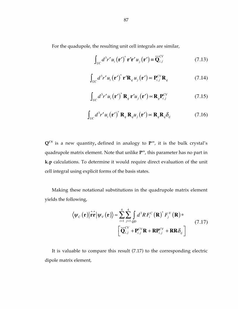
87
For the quadupole, the resulting unit cell integrals are similar,
d 3 ′r
UC∫ ui ′r( )* ′r ′r u j ′r( ) ≡ Q
i, jCV
(7.13)
d 3 ′rUC∫ ui ′r( )* ′r Rq u j ′r( )∝ Pi, jCVRq (7.14)
d 3 ′rUC∫ ui ′r( )*Rq ′r u j ′r( )∝RqPi, jCV (7.15)
d 3 ′rUC∫ ui ′r( )*Rq Rqu j ′r( )∝RqRqδ ij (7.16)
QCV is a new quantity, defined in analogy to Pcv, it is the bulk crystal’s
quadrupole matrix element. Note that unlike Pcv, this parameter has no part in
k.p calculations. To determine it would require direct evaluation of the unit
cell integral using explicit forms of the basis states.
Making these notational substitutions in the quadrupole matrix element
yields the following,
ψ C r( ) rr ψ V r( ) ≈ d 3RQD∫ Fi
C R( )* FjV R( )
j=1
4
∑i=1
4
∑ ∗
Q
i, jCV
+Pi, jCVR + RPi, jCV + RRδ ij⎡⎣
⎤⎦
(7.17)
It is valuable to compare this result (7.17) to the corresponding electric
dipole matrix element,

88
ψ C r( ) r ψ V r( ) ≈ d 3RQD∫ Fi
C R( )* FjV R( )
j=1
4
∑i=1
4
∑ ∗
Pi, jCV + Rδ ij⎡⎣ ⎤⎦
(7.18)
Notice that the dipole matrix element contains contributions from (1) the
dipole moment of the Bloch functions and (2) the dipole moment of the
envelope functions. Similarly by extension, the quadrupole matrix element
contains contributions from (1) the quadrupole moment of the Bloch
functions, (2) a combination of dipole moments of the Bloch functions and
envelope function, and (3) the quadrupole moment of the envelope functions.
We estimated the magnitude of the electric dipole and electric quadrupole
matrix elements. The electric dipole was numerically evaluated on a Se – Sh
transition and the electric quadrupole, on a S – P transition. Without access to
a numerical value for Qcv, we approximated this with the square of Pcv. We
find that the electric quadrupole and electric dipole are of the same order
magnitude (~ 0.1). Therefore, the quadrupole contribution is a factor of ~ 1/λ
smaller than the dipole. There is no way to explain a strong quadrupole
feature in the linear absorption spectrum on the basis of the overlap integrals
alone. The application of strong electric field gradients, discussed in Chapter
3, appears to be the only way to selectively enhance a quadrupole transition to
a strength comparable to the electric dipole.

89
References
1 I. Kang and F. W. Wise, Journal of the Optical Society of America B(Optical Physics) 14, 1632 (1997).
2 C. Cohen-Tannoudji, B. Diu, and F. Laloe, Quantum Mechanics (Wiley,New York, 1977).
3 J. R. Zurita-Sanchez and L. Novotny, Journal of the Optical Society ofAmerica B (Optical Physics) 19, 2722 (2002).